US11383269B2 - Curved micromachined ultrasonic transducer membranes - Google Patents
Curved micromachined ultrasonic transducer membranesDownload PDFInfo
- Publication number
- US11383269B2 US11383269B2US16/896,310US202016896310AUS11383269B2US 11383269 B2US11383269 B2US 11383269B2US 202016896310 AUS202016896310 AUS 202016896310AUS 11383269 B2US11383269 B2US 11383269B2
- Authority
- US
- United States
- Prior art keywords
- transducer
- membrane
- curved
- forming
- cavity
- Prior art date
- Legal status (The legal status is an assumption and is not a legal conclusion. Google has not performed a legal analysis and makes no representation as to the accuracy of the status listed.)
- Active, expires
Links
- 239000012528membraneSubstances0.000titleclaimsabstractdescription80
- 238000000034methodMethods0.000claimsabstractdescription39
- 239000011797cavity materialSubstances0.000claimsdescription105
- 238000001459lithographyMethods0.000claimsdescription9
- 229920002120photoresistant polymerPolymers0.000claimsdescription9
- 238000000059patterningMethods0.000claimsdescription8
- 238000005530etchingMethods0.000claimsdescription5
- 238000012546transferMethods0.000claimsdescription3
- 238000000137annealingMethods0.000claimsdescription2
- 239000003989dielectric materialSubstances0.000claimsdescription2
- 238000005498polishingMethods0.000claimsdescription2
- 239000000126substanceSubstances0.000claimsdescription2
- 238000002604ultrasonographyMethods0.000description28
- 239000000463materialSubstances0.000description27
- 230000008569processEffects0.000description17
- 239000000758substrateSubstances0.000description11
- 235000012431wafersNutrition0.000description11
- VYPSYNLAJGMNEJ-UHFFFAOYSA-NSilicium dioxideChemical compoundO=[Si]=OVYPSYNLAJGMNEJ-UHFFFAOYSA-N0.000description9
- 238000002161passivationMethods0.000description9
- 229910052581Si3N4Inorganic materials0.000description7
- 238000000623plasma-assisted chemical vapour depositionMethods0.000description7
- 238000012545processingMethods0.000description7
- HQVNEWCFYHHQES-UHFFFAOYSA-Nsilicon nitrideChemical compoundN12[Si]34N5[Si]62N3[Si]51N64HQVNEWCFYHHQES-UHFFFAOYSA-N0.000description7
- 238000012876topographyMethods0.000description7
- 238000004519manufacturing processMethods0.000description6
- 229910052751metalInorganic materials0.000description6
- 239000002184metalSubstances0.000description6
- 229910052681coesiteInorganic materials0.000description5
- 229910052906cristobaliteInorganic materials0.000description5
- 239000000377silicon dioxideSubstances0.000description5
- 229910052682stishoviteInorganic materials0.000description5
- 229910052905tridymiteInorganic materials0.000description5
- NRTOMJZYCJJWKI-UHFFFAOYSA-NTitanium nitrideChemical compound[Ti]#NNRTOMJZYCJJWKI-UHFFFAOYSA-N0.000description4
- 238000013459approachMethods0.000description4
- 230000008901benefitEffects0.000description4
- XUIMIQQOPSSXEZ-UHFFFAOYSA-NSiliconChemical compound[Si]XUIMIQQOPSSXEZ-UHFFFAOYSA-N0.000description3
- 229910052782aluminiumInorganic materials0.000description3
- 230000015572biosynthetic processEffects0.000description3
- 239000010949copperSubstances0.000description3
- 229910052710siliconInorganic materials0.000description3
- 239000010703siliconSubstances0.000description3
- 210000001519tissueAnatomy0.000description3
- 238000012285ultrasound imagingMethods0.000description3
- 229910045601alloyInorganic materials0.000description2
- 239000000956alloySubstances0.000description2
- XAGFODPZIPBFFR-UHFFFAOYSA-NaluminiumChemical compound[Al]XAGFODPZIPBFFR-UHFFFAOYSA-N0.000description2
- 239000003990capacitorSubstances0.000description2
- 239000011651chromiumSubstances0.000description2
- 229910052802copperInorganic materials0.000description2
- 238000010586diagramMethods0.000description2
- 238000009413insulationMethods0.000description2
- 229910052715tantalumInorganic materials0.000description2
- GUVRBAGPIYLISA-UHFFFAOYSA-Ntantalum atomChemical compound[Ta]GUVRBAGPIYLISA-UHFFFAOYSA-N0.000description2
- 239000010936titaniumSubstances0.000description2
- 229910016570AlCuInorganic materials0.000description1
- VYZAMTAEIAYCRO-UHFFFAOYSA-NChromiumChemical compound[Cr]VYZAMTAEIAYCRO-UHFFFAOYSA-N0.000description1
- RYGMFSIKBFXOCR-UHFFFAOYSA-NCopperChemical compound[Cu]RYGMFSIKBFXOCR-UHFFFAOYSA-N0.000description1
- RTAQQCXQSZGOHL-UHFFFAOYSA-NTitaniumChemical compound[Ti]RTAQQCXQSZGOHL-UHFFFAOYSA-N0.000description1
- QCWXUUIWCKQGHC-UHFFFAOYSA-NZirconiumChemical compound[Zr]QCWXUUIWCKQGHC-UHFFFAOYSA-N0.000description1
- 229910052804chromiumInorganic materials0.000description1
- 239000011248coating agentSubstances0.000description1
- 238000000576coating methodMethods0.000description1
- 230000000295complement effectEffects0.000description1
- 238000000151depositionMethods0.000description1
- 238000002059diagnostic imagingMethods0.000description1
- 201000010099diseaseDiseases0.000description1
- 208000037265diseases, disorders, signs and symptomsDiseases0.000description1
- 230000005284excitationEffects0.000description1
- 238000003384imaging methodMethods0.000description1
- 229910044991metal oxideInorganic materials0.000description1
- 150000004706metal oxidesChemical class0.000description1
- 238000001465metallisationMethods0.000description1
- 150000004767nitridesChemical class0.000description1
- 230000007170pathologyEffects0.000description1
- 230000035699permeabilityEffects0.000description1
- 238000001020plasma etchingMethods0.000description1
- 238000002360preparation methodMethods0.000description1
- 230000009467reductionEffects0.000description1
- 230000004044responseEffects0.000description1
- 239000000523sampleSubstances0.000description1
- 238000007789sealingMethods0.000description1
- 239000004065semiconductorSubstances0.000description1
- 210000004872soft tissueAnatomy0.000description1
- 230000005236sound signalEffects0.000description1
- MZLGASXMSKOWSE-UHFFFAOYSA-Ntantalum nitrideChemical compound[Ta]#NMZLGASXMSKOWSE-UHFFFAOYSA-N0.000description1
- 230000002123temporal effectEffects0.000description1
- 229910052719titaniumInorganic materials0.000description1
- WFKWXMTUELFFGS-UHFFFAOYSA-NtungstenChemical compound[W]WFKWXMTUELFFGS-UHFFFAOYSA-N0.000description1
- 229910052721tungstenInorganic materials0.000description1
- 239000010937tungstenSubstances0.000description1
- 229910052726zirconiumInorganic materials0.000description1
Images


Classifications
- B—PERFORMING OPERATIONS; TRANSPORTING
- B06—GENERATING OR TRANSMITTING MECHANICAL VIBRATIONS IN GENERAL
- B06B—METHODS OR APPARATUS FOR GENERATING OR TRANSMITTING MECHANICAL VIBRATIONS OF INFRASONIC, SONIC, OR ULTRASONIC FREQUENCY, e.g. FOR PERFORMING MECHANICAL WORK IN GENERAL
- B06B1/00—Methods or apparatus for generating mechanical vibrations of infrasonic, sonic, or ultrasonic frequency
- B06B1/02—Methods or apparatus for generating mechanical vibrations of infrasonic, sonic, or ultrasonic frequency making use of electrical energy
- B06B1/0292—Electrostatic transducers, e.g. electret-type
- B—PERFORMING OPERATIONS; TRANSPORTING
- B81—MICROSTRUCTURAL TECHNOLOGY
- B81C—PROCESSES OR APPARATUS SPECIALLY ADAPTED FOR THE MANUFACTURE OR TREATMENT OF MICROSTRUCTURAL DEVICES OR SYSTEMS
- B81C1/00—Manufacture or treatment of devices or systems in or on a substrate
- B81C1/00015—Manufacture or treatment of devices or systems in or on a substrate for manufacturing microsystems
- B81C1/00134—Manufacture or treatment of devices or systems in or on a substrate for manufacturing microsystems comprising flexible or deformable structures
- B81C1/00158—Diaphragms, membranes
- B—PERFORMING OPERATIONS; TRANSPORTING
- B81—MICROSTRUCTURAL TECHNOLOGY
- B81B—MICROSTRUCTURAL DEVICES OR SYSTEMS, e.g. MICROMECHANICAL DEVICES
- B81B2201/00—Specific applications of microelectromechanical systems
- B81B2201/02—Sensors
- B81B2201/0271—Resonators; ultrasonic resonators
- B—PERFORMING OPERATIONS; TRANSPORTING
- B81—MICROSTRUCTURAL TECHNOLOGY
- B81B—MICROSTRUCTURAL DEVICES OR SYSTEMS, e.g. MICROMECHANICAL DEVICES
- B81B2203/00—Basic microelectromechanical structures
- B81B2203/01—Suspended structures, i.e. structures allowing a movement
- B81B2203/0127—Diaphragms, i.e. structures separating two media that can control the passage from one medium to another; Membranes, i.e. diaphragms with filtering function
- B—PERFORMING OPERATIONS; TRANSPORTING
- B81—MICROSTRUCTURAL TECHNOLOGY
- B81B—MICROSTRUCTURAL DEVICES OR SYSTEMS, e.g. MICROMECHANICAL DEVICES
- B81B2203/00—Basic microelectromechanical structures
- B81B2203/03—Static structures
- B81B2203/0315—Cavities
- B—PERFORMING OPERATIONS; TRANSPORTING
- B81—MICROSTRUCTURAL TECHNOLOGY
- B81C—PROCESSES OR APPARATUS SPECIALLY ADAPTED FOR THE MANUFACTURE OR TREATMENT OF MICROSTRUCTURAL DEVICES OR SYSTEMS
- B81C2201/00—Manufacture or treatment of microstructural devices or systems
- B81C2201/01—Manufacture or treatment of microstructural devices or systems in or on a substrate
- B81C2201/0101—Shaping material; Structuring the bulk substrate or layers on the substrate; Film patterning
- B81C2201/0102—Surface micromachining
- B81C2201/0104—Chemical-mechanical polishing [CMP]
- B—PERFORMING OPERATIONS; TRANSPORTING
- B81—MICROSTRUCTURAL TECHNOLOGY
- B81C—PROCESSES OR APPARATUS SPECIALLY ADAPTED FOR THE MANUFACTURE OR TREATMENT OF MICROSTRUCTURAL DEVICES OR SYSTEMS
- B81C2201/00—Manufacture or treatment of microstructural devices or systems
- B81C2201/01—Manufacture or treatment of microstructural devices or systems in or on a substrate
- B81C2201/0101—Shaping material; Structuring the bulk substrate or layers on the substrate; Film patterning
- B81C2201/0102—Surface micromachining
- B81C2201/0105—Sacrificial layer
Definitions
- the present disclosurerelates generally to micromachined ultrasonic transducers and, more specifically, to fabrication techniques and associated structures for forming curved transducer membranes for micromachined ultrasound devices.
- Ultrasound devicesmay be used to perform diagnostic imaging and/or treatment, using sound waves with frequencies that are higher with respect to those audible to humans.
- Ultrasound imagingmay be used to see internal soft tissue body structures, for example to find a source of disease or to exclude any pathology.
- pulses of ultrasoundare transmitted into tissue (e.g., by using a probe)
- sound wavesare reflected off the tissue with different tissues reflecting varying degrees of sound.
- These reflected sound wavesmay then be recorded and displayed as an ultrasound image to the operator.
- the strength (amplitude) of the sound signal and the time it takes for the wave to travel through the bodyprovide information used to produce the ultrasound images.
- Some ultrasound imaging devicesmay be fabricated using micromachined ultrasonic transducers, including a flexible membrane suspended above a substrate. A cavity is located between part of the substrate and the membrane, such that the combination of the substrate, cavity and membrane form a variable capacitor.
- the membraneWhen actuated by an appropriate electrical signal, the membrane generates an ultrasound signal by vibration.
- the membraneIn response to receiving an ultrasound signal, the membrane is caused to vibrate and, as a result, generates an output electrical signal.
- a method of forming an ultrasonic transducer deviceincludes forming a curved membrane over a transducer cavity. A center portion of the curved membrane is closer to a bottom surface of the transducer cavity than with respect to radially outwardly disposed portions of the curved membrane.
- the methodmay include forming a curved sacrificial cavity material over a transducer bottom electrode, forming one or more membrane layers over the curved sacrificial cavity material and the transducer bottom electrode and removing the sacrificial cavity material.
- the methodmay include forming a sacrificial cavity material over a transducer bottom electrode; forming one or more membrane layers over the sacrificial cavity material and the transducer bottom electrode, wherein at least one of the one or more membrane layers is formed as a tensile layer; and removing the sacrificial cavity material, such that the at least one of the one or more tensile membrane layers results in the curved membrane.
- the methodmay include forming transducer cavities on a CMOS wafer; bonding a membrane wafer to the CMOS wafer to seal the transducer cavities; and performing an anneal to induce a curvature in the membrane wafer.
- an ultrasonic transducer devicein another aspect, includes a curved membrane formed over a transducer cavity. A center portion of the curved membrane is closer to a bottom surface of the transducer cavity than with respect to radially outwardly disposed portions of the curved membrane.
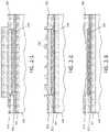
- FIGS. 1-1 through 1-9are a series of cross-sectional views illustrating an exemplary process flow for forming a micromachined ultrasound transducer device.
- FIGS. 2-1 through 2-9are a series of cross-sectional views illustrating an exemplary process flow for forming a micromachined ultrasound transducer device having a curved membrane according to an embodiment.
- FIGS. 3-1 through 3-3are a series of cross-sectional views illustrating an exemplary process flow for an alternate embodiment of a portion of the process flow of FIGS. 2-1 through 2-9 .
- FIGS. 4-1 through 4-7are a series of cross-sectional views illustrating an exemplary process flow for forming a micromachined ultrasound transducer device having a curved membrane according to another embodiment.
- FIG. 5is a flow diagram illustrating an exemplary process for forming a micromachined ultrasound transducer device having a curved membrane according to another embodiment.
- FIG. 6is a top view of an example ultrasonic transducer device formed using the process flow of FIGS. 2-1 through 2-9 , FIGS. 3-1 through 3-3 , FIGS. 4-1 through 4-7 and FIG. 5 .
- the techniques described hereinrelate to forming curved transducer membranes for micromachined ultrasound devices.
- Embodiments described hereinprovide a number of approaches for fabrication such curved transducer membranes including, for example: forming a curved profile in a sacrificial cavity material, which profile is adopted by subsequent membrane layer(s) formed on the sacrificial cavity material; utilizing film stress engineering to induce curvature by achieving a film stress gradient across the membrane thickness; and creating a pressure-induced curvature after the transducer cavity is sealed (e.g., by annealing at high pressure to fuse a collapsed cavity).
- the exemplary approachesare described in further detail herein.
- MUTmicromachined ultrasound transducer
- MUTsmay include capacitive micromachined ultrasound transducers (CMUTs) and piezoelectric micromachined ultrasound transducers (PMUTs), which can offer several advantages over more conventional transducer designs such as, for example, lower manufacturing costs and fabrication times and/or increased frequency bandwidth.
- CMUTscapacitive micromachined ultrasound transducers
- PMUTspiezoelectric micromachined ultrasound transducers
- the basic structureis a parallel plate capacitor with a rigid bottom electrode and a top electrode residing on or within a flexible membrane. Thus, a cavity is defined between the bottom and top electrodes.
- the CMUT transducermay be formed directly integrated on an integrated circuit that controls the operation of the transducer.
- One way of manufacturing CMUT ultrasound deviceis to bond a membrane substrate to an integrated circuit substrate, such a CMOS substrate. This may be performed at temperatures sufficiently low enough to prevent damage to the devices of the integrated circuit.
- a substratee.g., a complementary metal oxide semiconductor (CMOS) substrate, such as silicon
- CMOS substratesuch as silicon
- the CMOS substrate 100may include, but is not necessarily limited to, CMOS circuits, wiring layers, redistribution layers, and insulation/passivation layers (e.g., passivation layer 102 , such as SiO 2 ).
- the electrode metal stack 104may include one or more individual metal layers such as, for example, aluminum (Al), titanium (Ti), titanium nitride (TiN), tantalum (Ta), tantalum nitride (TaN), copper (Cu), AlCu, and alloys thereof.
- the electrode metal stack 104may be formed by subtractive processes (e.g., blanket metal deposition and etching) or by damascene processes (e.g., insulation layer patterning followed by metal fill and planarization).
- a first dielectric layer 106is formed over the passivation layer 102 and patterned bottom electrode 104 .
- the first dielectric layer 106may be a high dielectric constant (high-k) layer such as silicon nitride (SiN), silicon oxynitride (SiON), halfnium oxide (HfO 2 ), etc. formed at thickness of about 10-100 nanometers (nm).
- high-khigh dielectric constant
- SiNsilicon nitride
- SiONsilicon oxynitride
- HfO 2halfnium oxide
- other dielectric materialssuch as oxides of aluminum, zirconium, and/or tantalum may also be used.
- a nitride based dielectricis used for layer 106 , there may be some topography associated with the layer as shown in FIG. 1-2 .
- the topographymay remain or, alternatively, may be planarized to the top of the bottom electrode 104 .
- the first dielectric layer 106may be formed as a bi-layer if desired in order to, for example, provide additional protection for electrode structures from subsequently introduced cavity release etchant materials.
- a sacrificial cavity material 108may then be formed over the structure of FIG. 1-2 and lithographically patterned and etched, resulting in the structure illustrated in FIG. 1-3 .
- the sacrificial cavity material 108may include one or more layers of a material or materials such as, for example, Al, Cu, chromium (Cr), Si, tungsten (W), TiN or alloys thereof, formed at a thickness of about 200 nm.
- a second dielectric layer 110is formed over the first dielectric layer 106 and sacrificial cavity material 108 .
- the second dielectric layer 110may be formed from the same material and at the same thickness as the first dielectric layer 106 . Then, as shown in FIG.
- a patterned top electrode 112is formed over the second dielectric layer 110 .
- the top electrode 112may be formed from the same material(s) as the bottom electrode 104 and, optionally, at the same or different thickness (e.g., thinner) than the bottom electrode 104 .
- a patterned width of the top electrode 112may be smaller than the bottom electrode 104 (e.g., as shown at the top right portion of FIG. 1-5 ), or otherwise designed so as to allow access to the sacrificial cavity material 108 for subsequent removal thereof.
- a third dielectric layer 114is formed over the second dielectric layer 110 and top electrode 112 .
- the third dielectric layer 114may be formed from the same material(s) as the first and second dielectric layers 106 , 110 and, optionally, at a greater thickness the first and second dielectric layers 106 , 110 (e.g., 1000 nm).
- an access hole 116is formed through the third and second dielectric layer 114 , 110 , such as by etching for example, to expose a portion of the sacrificial cavity material 108 .
- the sacrificial cavity material 108is etched to create an ultrasound transducer cavity 118 .
- a fourth dielectric layer 120is formed over the structure to seal the cavity 118 .
- the fourth dielectric layer 120may be formed from the same material as one or more of the previously formed dielectric layers, and at a greater thickness (e.g., about 5000 nm). From this point, additional processing may continue to complete the fabrication of an operational ultrasound transducer array, the details of which are beyond the scope of the present disclosure.
- the transducer membranee.g., second dielectric layer 110
- the bottom surface of the cavity 118e.g., the first dielectric layer 106
- This positionmay be indicative of the so-called “collapse mode” of operation as known in the art.
- a “collapse mode”(also used interchangeably with the term “collapsed mode”) refers to a mode of transducer operation in which at least one portion of a micromachined ultrasonic transducer membrane is mechanically fixed and at least one portion of the membrane is free to vibrate based on a changing voltage differential between the electrode and the membrane.
- One possible advantage to operating a micromachined ultrasonic transducer in collapse modemay be optimize the acoustic power (output pressure) produced by the transducer.
- a sufficient DC bias voltageis needed such that, the greater the initial distance between the membrane and the bottom of the transducer cavity, the higher the DC bias voltage needed.
- FIGS. 2-1 through 2-9there is shown are a series of cross-sectional views illustrating an exemplary process flow for forming a micromachined ultrasound transducer device having a curved membrane according to an embodiment.
- CMPchemical mechanical planarization/polishing
- FIG. 2-1illustrates a point in processing after patterning of the sacrificial cavity material 108 (e.g., as was shown in FIG. 1-3 ). However, rather than depositing a relatively thin second dielectric layer (e.g., layer 110 shown in FIG. 1-4 ), FIG. 2-1 additionally illustrates the formation of a relatively thick CMP support dielectric layer 200 over the first dielectric layer 106 and sacrificial cavity material 108 .
- the CMP support dielectric layer 200may be the same material as the first dielectric layer 106 , but formed at a greater thickness (e.g., 1000 nm or more).
- the CMP support dielectric layer 200is patterned as illustrated in preparation for a CMP operation on the sacrificial cavity material 108 .
- the CMP support dielectric layer 200may be patterned so as to be completely removed directly above the sacrificial cavity material 108 .
- selected portions (indicted by dashes in FIG. 2-1 ) of the CMP support dielectric layer 200may remain over the sacrificial cavity material 108 after patterning.
- the CMP operationresults in the sacrificial cavity material 108 becoming concave in shape (i.e., being thinner at a central region and thicker at outer regions adjacent the CMP support dielectric layer 200 ).
- the use of a bilayer stack for the sacrificial cavity material 108can assist in robust stopping of the CMP at a certain thickness of the sacrificial material, while the dishing is confined only to the top layer. From this point, similar steps may be performed as was previously described with respect to FIGS. 1-4 through 1-9 , but with different structural results owning to the concave shape of the sacrificial cavity material 108 .
- a second dielectric layer 110is formed over the CMP support dielectric layer 200 and sacrificial cavity material 108 .
- the second dielectric layer 110may be formed from a same material and at a same thickness as the first dielectric 106 and, notably, is conformal with the concave shape of the sacrificial cavity material 108 .
- a patterned top electrode 112is formed over the second dielectric layer 110 .
- the top electrode 112may be formed from the same material(s) as the bottom electrode 104 and, optionally, at the same or different thickness (e.g., thinner) than the bottom electrode 104 .
- a patterned width of the top electrode 112may be smaller than the bottom electrode 104 (e.g., as shown at the top right portion of FIG. 2-5 ) so as to allow access to the sacrificial cavity material 108 for subsequent removal thereof.
- a third dielectric layer 114is formed over the second dielectric layer 110 and top electrode 112 .
- the third dielectric layer 114may be formed from the same material(s) as the first and second dielectric layers 106 , 110 and, optionally, at a greater thickness the first and second dielectric layers 106 , 110 (e.g., 1000 nm).
- an access hole 116is formed through the third and second dielectric layer 114 , 110 , such as by etching for example, to expose a portion of the sacrificial cavity material 108 .
- the sacrificial cavity material 108is etched to create an ultrasound transducer cavity 118 .
- a fourth dielectric layer 120is formed over the structure to seal the cavity 118 .
- the fourth dielectric layer 120may be formed from the same material as one or more of the previously formed dielectric layers, and at a greater thickness (e.g., about 5000 nm).
- a possible advantage of the structure illustrated in FIG. 2-9is improved transducer performance due to (for example) a reduction in voltage required for membrane collapse, in that the region of the second dielectric layer 110 corresponding to the center of the transducer cavity 118 is physically closer to the first dielectric layer 106 as compared to the embodiment of FIG. 1-9 . Accordingly, a smaller voltage may bring the transducer into collapse such that the second dielectric layer 110 is in physical contact with the first dielectric layer 106 during transducer operation.
- FIGS. 3-1 through 3-3are a series of cross-sectional views illustrating an exemplary process flow for an alternate embodiment of a portion of the process flow of FIGS. 2-1 through 2-9 .
- grayscale lithographyis used to create a 3D topography in a patterned resist material, which 3D topography is in turn transferred into a sacrificial material.
- the surface topography of the sacrificial materialdetermines the curvature of subsequent layers (e.g., a membrane) deposited on the sacrificial material, where the curvature remains after removal of the sacrificial material.
- a sacrificial cavity material layer 108is formed over a first dielectric layer 106 , patterned bottom electrode 104 , passivation layer 102 and CMOS substrate 100 .
- the layers in FIG. 3-1may be substantially similar to those depicted in the previously described embodiments.
- a photoresist layer 300is formed over the sacrificial cavity material layer 108 and patterned in the manner depicted to result in a concave structure. Again, this may be accomplished via grayscale lithography, for example, which spatially modulates ultraviolet (UV) dosage of the resist material, thereby varying the depth at which the resist material is developed.
- UVultraviolet
- the resulting patternmay then be transferred into the sacrificial cavity material layer 108 , such as by plasma etching for example, to result in the structure illustrated in FIG. 3-3 .
- An etch recipemay be tuned for low etch selectivity between the resist material and the etched sacrificial cavity material in order to transfer the concave pattern into the sacrificial cavity material layer 108 .
- the sacrificial cavity material layer 108may be shaped by first performing the grayscale lithography to create the concave regions in the sacrificial cavity material layer 108 corresponding to the cavity regions, followed by using standard lithography to remove the sacrificial cavity material layer material everywhere else.
- the reversemay also be performed (standard lithography followed by grayscale lithography). It may be advantageous to divide up the processing into separate grayscale and standard pattering due to the complexities associated with grayscale lithography and 3D etch transfer, which conditions may not be compatible with simultaneously clearing the remaining sacrificial cavity material in a same step. From this point, additional processing steps may be performed similar to those illustrated in FIGS. 2-4 through 2-9 to complete the transducer structure.
- FIGS. 4-1 through 4-7there is shown a series of cross-sectional views illustrating an exemplary process flow for forming a micromachined ultrasound transducer device having a curved membrane according to another embodiment.
- FIG. 4-1is similar to the embodiment of FIG. 1-1 (showing a CMOS substrate 100 , a passivation layer 102 and a patterned bottom electrode 104 ), and further illustrating an optional processing variation in which additional passivation material may be formed over the patterned bottom electrode 104 followed by planarization so that the passivation layer 102 and the bottom electrode 104 are substantially co-planar.
- a first dielectric layer 106 formed over the passivation layer 102 and patterned bottom electrode 104may be substantially planar, as illustrated in FIG. 4-2 .
- FIG. 4-2further illustrates the formation of a patterned sacrificial cavity material layer 108 .
- a second dielectric layer 110is formed over the first dielectric layer 106 and the patterned sacrificial cavity material layer 108 .
- second dielectric layer 110may be formed by plasma enhanced chemical vapor deposition (PECVD) silicon nitride.
- PECVDplasma enhanced chemical vapor deposition
- a patterned top electrode 112is formed over the second dielectric layer 110 .
- the top electrodemay be a multiple layer stack including TiN/Al/TiN at a total thickness of about 300 nm. From this point, stress engineering techniques may be used to produce a desired transducer membrane curvature.
- film stress in the individual PECVD layerscan be tuned to induce a controlled curvature in the membrane by adjusting the recipes of the PECVD process.
- a plasma excitation sourcemay comprise both “high frequency” and “low frequency” sources, and adjusting the power between these sources can in turn adjust the stress in a silicon nitride film.
- low stress filmsmay be deposited at a bottom of the transducer membrane, with tensile stress being increased with each subsequent coating.
- the membranemay be curved after removal of the sacrificial cavity material layer 108 .
- low stress filmsmay be deposited for each membrane layer up to the sealing of the cavity.
- the membrane curvature(which may be relatively low at this point) can then be measured, after which a final tensile film is deposited to create the desired membrane curvature.
- a third dielectric layer 114is formed over the second dielectric layer 110 and the patterned top electrode 112 .
- the third dielectric layer 114may be a PECVD silicon nitride layer formed at a thickness of about 100 nm and having a tensile strength of about 25 MPa.
- the third dielectric layer 114may be a substantially stress-free PECVD silicon nitride layer formed at a thickness of about 100 nm.
- an access hole 116is formed through the third and second dielectric layer 114 , 110 , such as by etching for example, to access and remove the sacrificial cavity material 108 and to create an ultrasound transducer cavity 118 .
- the third dielectric layer 114is formed as a tensile layer
- the resulting structuremay assume an initial curvature as shown in FIG. 4-6 .
- the structuremay at this point in processing resemble that illustrated in FIG. 1-8 .
- FIG. 4-7then illustrates the formation of a fourth dielectric layer 120 over the structure to seal the cavity 118 .
- the fourth dielectric layer 120may be formed from the same material as one or more of the previously formed dielectric layers (e.g., PECVD silicon nitride), and at a greater thickness (e.g., about 5000 nm).
- the fourth dielectric layer 120may have a tensile strength of about 50 MPa.
- the fourth dielectric layer 120may be formed so as to be substantially stress-free for an initial portion of its thickness (e.g., for about 2000 nm), followed by being deposited at a tensile strength of about 50 MPa for a remaining portion of its thickness (e.g., for about 3000 nm).
- FIG. 5is a flow diagram illustrating an exemplary process 500 for forming a micromachined ultrasound transducer device having a curved membrane according to another embodiment.
- transducer cavitiesare formed on a CMOS wafer using a low thermal budget bondable material; that is, using a material where bonding temperatures and times of the material are compatible with other structures on the wafers, such as CMOS devices.
- An example of the transducer cavity materialmay be SiO 2 .
- a membrane waferis boned to the CMOS wafer in order to seal the transduce cavities.
- the membrane wafermay also be SiO 2 , such that that the bonding operation of the membrane wafer to the CMOS wafer comprises an SiO 2 to SiO 2 bond.
- the bonded structureis subjected to an anneal at a gas pressure that is high enough to induce a curvature of the membrane.
- the pressure of anneal chambermay be in excess of 100 bar.
- the time and temperature of the annealmay be sufficient to induce bonding of the membrane to the bottom of the cavity.
- the annealmay be from about 250° C. to 400° C. for about 1 hour to about 4 hours.
- the gasmay include one or more species with low permeability through the membrane and other structures, such as Ar or N 2 .
- FIG. 6illustrates a top view of an example ultrasound transducer device 600 formed using any of the process flow sequences described herein.
- the transducer deviceincludes an array of individual transducers 602 , such as those formed by the exemplary processing embodiments described above.
- the exemplary geometric structure of this portion of the ultrasound transducer 602is generally circular in shape, other configurations are also contemplated such as for example, rectangular, hexagonal, octagonal, and other multi-sides shapes, etc.
- the specific number of transducers 602 shown in FIG. 6should not be construed in any limiting sense, and may include any number suitable for a desired imaging application, which may be for example on the order of tens, hundreds, thousands, tens of thousands or more.
- FIG. 6further illustrates an example location of metal 604 that may distribute an electrical signal to the membranes (upper electrodes) of the transducers 602 .
- the embodimentscan be implemented in any of numerous ways.
- the embodimentsmay be implemented using hardware, software or a combination thereof.
- the software codecan be executed on any suitable processor (e.g., a microprocessor) or collection of processors, whether provided in a single computing device or distributed among multiple computing devices.
- any component or collection of components that perform the functions described abovecan be generically considered as one or more controllers that control the above-discussed functions.
- the one or more controllerscan be implemented in numerous ways, such as with dedicated hardware, or with general purpose hardware (e.g., one or more processors) that is programmed using microcode or software to perform the functions recited above.
- the inventionmay be embodied as a method, of which an example has been provided.
- the acts performed as part of the methodmay be ordered in any suitable way. Accordingly, embodiments may be constructed in which acts are performed in an order different than illustrated, which may include performing some acts simultaneously, even though shown as sequential acts in illustrative embodiments.
Landscapes
- Engineering & Computer Science (AREA)
- Manufacturing & Machinery (AREA)
- Microelectronics & Electronic Packaging (AREA)
- Mechanical Engineering (AREA)
- Transducers For Ultrasonic Waves (AREA)
- Ultra Sonic Daignosis Equipment (AREA)
Abstract
Description
Claims (7)
Priority Applications (1)
| Application Number | Priority Date | Filing Date | Title |
|---|---|---|---|
| US16/896,310US11383269B2 (en) | 2019-06-10 | 2020-06-09 | Curved micromachined ultrasonic transducer membranes |
Applications Claiming Priority (2)
| Application Number | Priority Date | Filing Date | Title |
|---|---|---|---|
| US201962859634P | 2019-06-10 | 2019-06-10 | |
| US16/896,310US11383269B2 (en) | 2019-06-10 | 2020-06-09 | Curved micromachined ultrasonic transducer membranes |
Publications (2)
| Publication Number | Publication Date |
|---|---|
| US20200384503A1 US20200384503A1 (en) | 2020-12-10 |
| US11383269B2true US11383269B2 (en) | 2022-07-12 |
Family
ID=73651308
Family Applications (1)
| Application Number | Title | Priority Date | Filing Date |
|---|---|---|---|
| US16/896,310Active2040-11-28US11383269B2 (en) | 2019-06-10 | 2020-06-09 | Curved micromachined ultrasonic transducer membranes |
Country Status (2)
| Country | Link |
|---|---|
| US (1) | US11383269B2 (en) |
| WO (1) | WO2020251915A1 (en) |
Families Citing this family (2)
| Publication number | Priority date | Publication date | Assignee | Title |
|---|---|---|---|---|
| TW202239483A (en) | 2021-03-04 | 2022-10-16 | 美商蝴蝶營運公司 | Capacitive micromachined ultrasonic transducers (cmuts) having non-uniform pedestals |
| US20230381815A1 (en)* | 2022-05-24 | 2023-11-30 | Taiwan Semiconductor Manufacturing Co., Ltd. | Transducer device and method of manufacture |
Citations (35)
| Publication number | Priority date | Publication date | Assignee | Title |
|---|---|---|---|---|
| US6430109B1 (en) | 1999-09-30 | 2002-08-06 | The Board Of Trustees Of The Leland Stanford Junior University | Array of capacitive micromachined ultrasonic transducer elements with through wafer via connections |
| US6694817B2 (en) | 2001-08-21 | 2004-02-24 | Georgia Tech Research Corporation | Method and apparatus for the ultrasonic actuation of the cantilever of a probe-based instrument |
| US6958255B2 (en) | 2002-08-08 | 2005-10-25 | The Board Of Trustees Of The Leland Stanford Junior University | Micromachined ultrasonic transducers and method of fabrication |
| US20100207484A1 (en)* | 2007-09-25 | 2010-08-19 | Canon Kabushiki Kaisha | Electromechanical transducer and manufacturing method therefor |
| US20100225200A1 (en) | 2009-03-05 | 2010-09-09 | Mario Kupnik | Monolithic integrated CMUTs fabricated by low-temperature wafer bonding |
| US20100244162A1 (en) | 2007-09-19 | 2010-09-30 | Richard Ian Laming | Mems device with reduced stress in the membrane and manufacturing method |
| US7846102B2 (en) | 2007-10-18 | 2010-12-07 | The Board Of Trustees Of The Leland Stanford Junior University | Direct wafer bonded 2-D CUMT array |
| US20110055447A1 (en) | 2008-05-07 | 2011-03-03 | Signostics Limited | Docking system for medical diagnostic scanning using a handheld device |
| US20110316100A1 (en) | 2009-11-06 | 2011-12-29 | Kim Yong-Kook | Mems microphone and method for manufacturing same |
| US20120010538A1 (en) | 2007-09-17 | 2012-01-12 | Koninklijke Philips Electronics N.V. | Pre-collapsed cmut with mechanical collapse retention |
| WO2013005486A1 (en) | 2011-07-04 | 2013-01-10 | オリンパスメディカルシステムズ株式会社 | Electrostatic capacitance type ultrasonic transducer and electronic device |
| US20130210175A1 (en) | 2010-07-26 | 2013-08-15 | Paul A. Hoisington | Forming a Device Having a Curved Piezoelectric Membrane |
| US20140192397A1 (en) | 2013-01-04 | 2014-07-10 | Texas Instruments Incorporated | Mems device with sloped support |
| US9067779B1 (en) | 2014-07-14 | 2015-06-30 | Butterfly Network, Inc. | Microfabricated ultrasonic transducers and related apparatus and methods |
| US20150194320A1 (en)* | 2014-01-08 | 2015-07-09 | International Business Machines Corporation | Metallic mask patterning process for minimizing collateral etch of an underlayer |
| US9242275B2 (en) | 2013-03-15 | 2016-01-26 | Butterfly Networks, Inc. | Complementary metal oxide semiconductor (CMOS) ultrasonic transducers and methods for forming the same |
| US9499392B2 (en) | 2013-02-05 | 2016-11-22 | Butterfly Network, Inc. | CMOS ultrasonic transducers and related apparatus and methods |
| US9505030B2 (en) | 2014-04-18 | 2016-11-29 | Butterfly Network, Inc. | Ultrasonic transducers in complementary metal oxide semiconductor (CMOS) wafers and related apparatus and methods |
| US20170215846A1 (en) | 2014-01-24 | 2017-08-03 | The Regents Of The University Of California | Medical Devices comprising curved Piezoelectric Transducers |
| US20170360413A1 (en) | 2016-06-20 | 2017-12-21 | Butterfly Network, Inc. | Universal ultrasound device and related apparatus and methods |
| US20170360399A1 (en) | 2016-06-20 | 2017-12-21 | Jonathan M. Rothberg | Universal ultrasound device and related apparatus and methods |
| US9987661B2 (en) | 2015-12-02 | 2018-06-05 | Butterfly Network, Inc. | Biasing of capacitive micromachined ultrasonic transducers (CMUTs) and related apparatus and methods |
| US20180369862A1 (en) | 2017-06-21 | 2018-12-27 | Butterfly Network, Inc. | Microfabricated ultrasonic transducer having individual cells with electrically isolated electrode sections |
| US20190001159A1 (en) | 2017-06-30 | 2019-01-03 | Butterfly Network, Inc. | Steerable high-intensity focused ultrasound (hifu) elements |
| US20190000422A1 (en) | 2017-06-30 | 2019-01-03 | Butterfly Network, Inc. | Elasticity imaging in high intensity focused ultrasound |
| US10196261B2 (en) | 2017-03-08 | 2019-02-05 | Butterfly Network, Inc. | Microfabricated ultrasonic transducers and related apparatus and methods |
| US20190069842A1 (en) | 2017-09-07 | 2019-03-07 | Butterfly Network, Inc. | Wrist bound ultrasound-on-a-chip device |
| US10446132B2 (en) | 2016-12-13 | 2019-10-15 | Butterfly Network, Inc. | Acoustic lens and applications thereof |
| US10497856B2 (en) | 2016-06-20 | 2019-12-03 | Butterfly Network, Inc. | Electrical contact arrangement for microfabricated ultrasonic transducer |
| US20190366382A1 (en)* | 2018-05-31 | 2019-12-05 | Canon Kabushiki Kaisha | Capacitive micromachined ultrasonic transducer and manufacturing method thereof |
| US20200093463A1 (en) | 2018-09-21 | 2020-03-26 | Butterfly Network, Inc. | Acoustic damping for ultrasound imaging devices |
| US20200163654A1 (en) | 2018-11-28 | 2020-05-28 | Butterfly Network, Inc. | Method and apparatus to calibrate ultrasound transducers |
| US20200222940A1 (en)* | 2019-01-15 | 2020-07-16 | Hitachi, Ltd. | Ultrasonic Transducer, Manufacturing Method Thereof, and Ultrasonic Imaging Apparatus |
| US20200324318A1 (en)* | 2019-04-12 | 2020-10-15 | Butterfly Network, Inc. | Segmented getter openings for micromachined ultrasound transducer devices |
| US20210307172A1 (en)* | 2016-09-02 | 2021-09-30 | Intel Corporation | An apparatus with embedded fine line space in a cavity, and a method for forming the same |
- 2020
- 2020-06-09USUS16/896,310patent/US11383269B2/enactiveActive
- 2020-06-09WOPCT/US2020/036735patent/WO2020251915A1/ennot_activeCeased
Patent Citations (50)
| Publication number | Priority date | Publication date | Assignee | Title |
|---|---|---|---|---|
| US6430109B1 (en) | 1999-09-30 | 2002-08-06 | The Board Of Trustees Of The Leland Stanford Junior University | Array of capacitive micromachined ultrasonic transducer elements with through wafer via connections |
| US6694817B2 (en) | 2001-08-21 | 2004-02-24 | Georgia Tech Research Corporation | Method and apparatus for the ultrasonic actuation of the cantilever of a probe-based instrument |
| US6958255B2 (en) | 2002-08-08 | 2005-10-25 | The Board Of Trustees Of The Leland Stanford Junior University | Micromachined ultrasonic transducers and method of fabrication |
| US20120010538A1 (en) | 2007-09-17 | 2012-01-12 | Koninklijke Philips Electronics N.V. | Pre-collapsed cmut with mechanical collapse retention |
| US20100244162A1 (en) | 2007-09-19 | 2010-09-30 | Richard Ian Laming | Mems device with reduced stress in the membrane and manufacturing method |
| US20100207484A1 (en)* | 2007-09-25 | 2010-08-19 | Canon Kabushiki Kaisha | Electromechanical transducer and manufacturing method therefor |
| US7846102B2 (en) | 2007-10-18 | 2010-12-07 | The Board Of Trustees Of The Leland Stanford Junior University | Direct wafer bonded 2-D CUMT array |
| US20110055447A1 (en) | 2008-05-07 | 2011-03-03 | Signostics Limited | Docking system for medical diagnostic scanning using a handheld device |
| US20100225200A1 (en) | 2009-03-05 | 2010-09-09 | Mario Kupnik | Monolithic integrated CMUTs fabricated by low-temperature wafer bonding |
| US8402831B2 (en) | 2009-03-05 | 2013-03-26 | The Board Of Trustees Of The Leland Standford Junior University | Monolithic integrated CMUTs fabricated by low-temperature wafer bonding |
| US20110316100A1 (en) | 2009-11-06 | 2011-12-29 | Kim Yong-Kook | Mems microphone and method for manufacturing same |
| US20130210175A1 (en) | 2010-07-26 | 2013-08-15 | Paul A. Hoisington | Forming a Device Having a Curved Piezoelectric Membrane |
| WO2013005486A1 (en) | 2011-07-04 | 2013-01-10 | オリンパスメディカルシステムズ株式会社 | Electrostatic capacitance type ultrasonic transducer and electronic device |
| US20140192397A1 (en) | 2013-01-04 | 2014-07-10 | Texas Instruments Incorporated | Mems device with sloped support |
| US9499392B2 (en) | 2013-02-05 | 2016-11-22 | Butterfly Network, Inc. | CMOS ultrasonic transducers and related apparatus and methods |
| US9533873B2 (en) | 2013-02-05 | 2017-01-03 | Butterfly Network, Inc. | CMOS ultrasonic transducers and related apparatus and methods |
| US9242275B2 (en) | 2013-03-15 | 2016-01-26 | Butterfly Networks, Inc. | Complementary metal oxide semiconductor (CMOS) ultrasonic transducers and methods for forming the same |
| US20180186628A1 (en) | 2013-03-15 | 2018-07-05 | Butterfly Network, Inc. | Complementary metal oxide semiconductor (cmos) ultrasonic transducers and methods for forming the same |
| US20150194320A1 (en)* | 2014-01-08 | 2015-07-09 | International Business Machines Corporation | Metallic mask patterning process for minimizing collateral etch of an underlayer |
| US20170215846A1 (en) | 2014-01-24 | 2017-08-03 | The Regents Of The University Of California | Medical Devices comprising curved Piezoelectric Transducers |
| US9505030B2 (en) | 2014-04-18 | 2016-11-29 | Butterfly Network, Inc. | Ultrasonic transducers in complementary metal oxide semiconductor (CMOS) wafers and related apparatus and methods |
| US9067779B1 (en) | 2014-07-14 | 2015-06-30 | Butterfly Network, Inc. | Microfabricated ultrasonic transducers and related apparatus and methods |
| WO2016011000A1 (en) | 2014-07-14 | 2016-01-21 | Butterfly Network, Inc. | Microfabricated ultrasonic transducers and related apparatus and methods |
| US10272471B2 (en) | 2015-12-02 | 2019-04-30 | Butterfly Network, Inc. | Biasing of capacitive micromachined ultrasonic transducers (CMUTs) and related apparatus and methods |
| US9987661B2 (en) | 2015-12-02 | 2018-06-05 | Butterfly Network, Inc. | Biasing of capacitive micromachined ultrasonic transducers (CMUTs) and related apparatus and methods |
| US20170360414A1 (en) | 2016-06-20 | 2017-12-21 | Butterfly Network, Inc. | Universal ultrasound device and related apparatus and methods |
| US20190000418A1 (en) | 2016-06-20 | 2019-01-03 | Butterfly Network, Inc. | Universal ultrasound device and related apparatus and methods |
| US20170360397A1 (en) | 2016-06-20 | 2017-12-21 | Butterfly Network, Inc. | Universal ultrasound device and related apparatus and methods |
| WO2017222964A1 (en) | 2016-06-20 | 2017-12-28 | Butterfly Network, Inc. | Universal ultrasound device and related apparatus and methods |
| US20170360405A1 (en) | 2016-06-20 | 2017-12-21 | Butterfly Network, Inc. | Universal ultrasound device and related apparatus and methods |
| US20170360399A1 (en) | 2016-06-20 | 2017-12-21 | Jonathan M. Rothberg | Universal ultrasound device and related apparatus and methods |
| US10497856B2 (en) | 2016-06-20 | 2019-12-03 | Butterfly Network, Inc. | Electrical contact arrangement for microfabricated ultrasonic transducer |
| US20170360415A1 (en) | 2016-06-20 | 2017-12-21 | Butterfly Network, Inc. | Universal ultrasound device and related apparatus and methods |
| US20170360413A1 (en) | 2016-06-20 | 2017-12-21 | Butterfly Network, Inc. | Universal ultrasound device and related apparatus and methods |
| US20200066966A1 (en) | 2016-06-20 | 2020-02-27 | Butterfly Network, Inc. | Electrical contact arrangement for microfabricated ultrasonic transducer |
| US20210307172A1 (en)* | 2016-09-02 | 2021-09-30 | Intel Corporation | An apparatus with embedded fine line space in a cavity, and a method for forming the same |
| US10446132B2 (en) | 2016-12-13 | 2019-10-15 | Butterfly Network, Inc. | Acoustic lens and applications thereof |
| US20190362698A1 (en) | 2016-12-13 | 2019-11-28 | Butterfly Network, Inc. | Acoustic lens and applications thereof |
| US10196261B2 (en) | 2017-03-08 | 2019-02-05 | Butterfly Network, Inc. | Microfabricated ultrasonic transducers and related apparatus and methods |
| US20190047850A1 (en) | 2017-03-08 | 2019-02-14 | Butterfly Network, Inc. | Microfabricated ultrasonic transducers and related apparatus and methods |
| US10672974B2 (en) | 2017-03-08 | 2020-06-02 | Butterfly Network, Inc. | Microfabricated ultrasonic transducers and related apparatus and methods |
| US20180369862A1 (en) | 2017-06-21 | 2018-12-27 | Butterfly Network, Inc. | Microfabricated ultrasonic transducer having individual cells with electrically isolated electrode sections |
| US20190001159A1 (en) | 2017-06-30 | 2019-01-03 | Butterfly Network, Inc. | Steerable high-intensity focused ultrasound (hifu) elements |
| US20190000422A1 (en) | 2017-06-30 | 2019-01-03 | Butterfly Network, Inc. | Elasticity imaging in high intensity focused ultrasound |
| US20190069842A1 (en) | 2017-09-07 | 2019-03-07 | Butterfly Network, Inc. | Wrist bound ultrasound-on-a-chip device |
| US20190366382A1 (en)* | 2018-05-31 | 2019-12-05 | Canon Kabushiki Kaisha | Capacitive micromachined ultrasonic transducer and manufacturing method thereof |
| US20200093463A1 (en) | 2018-09-21 | 2020-03-26 | Butterfly Network, Inc. | Acoustic damping for ultrasound imaging devices |
| US20200163654A1 (en) | 2018-11-28 | 2020-05-28 | Butterfly Network, Inc. | Method and apparatus to calibrate ultrasound transducers |
| US20200222940A1 (en)* | 2019-01-15 | 2020-07-16 | Hitachi, Ltd. | Ultrasonic Transducer, Manufacturing Method Thereof, and Ultrasonic Imaging Apparatus |
| US20200324318A1 (en)* | 2019-04-12 | 2020-10-15 | Butterfly Network, Inc. | Segmented getter openings for micromachined ultrasound transducer devices |
Non-Patent Citations (7)
| Title |
|---|
| Daft et al., Microfabricated Ultrasonic Transducers Monolithically Integrated with High Voltage Electronics. Proc Ultrason Symp. 2004;493-6. |
| Gurun et al., Front-end CMOS Electronics for Monolithic Integration with CMUT Arrays: Circuit Design and Initial Experimental Results. Proc Ultrason Symp. 2008;390-3. |
| International Search Report and Written Opinion dated Sep. 17, 2020 in connection with International Application No. PCT/US2020/036735. |
| Kalra, Advanced Source/Drain Technologies for Nanoscale CMOS. Dissertation submitted for Ph.D Engineering—Electrical engineering and Computer Sciences. Univ California Berkeley. 2008; 46 pages. |
| Kupnik et al., CMUT Fabrication Based on a Thick Buried Oxide Layer. Proc IEEE Ultrason Symp. Oct. 2010;2010:547-550. doi:10.1109/ULTSYM.2010.5935935. Epub Jun. 8, 2012. 10 pages. |
| Kupnik et al., Wafer-Bonded CMUT Meets CMOS. 2010 CMOS Emerging Technology Workshop. May 21, 2010;1-22. |
| PCT/US2020/036735, Sep. 17, 2020, International Search Report and Written Opinion. |
Also Published As
| Publication number | Publication date |
|---|---|
| WO2020251915A1 (en) | 2020-12-17 |
| US20200384503A1 (en) | 2020-12-10 |
Similar Documents
| Publication | Publication Date | Title |
|---|---|---|
| US11638931B2 (en) | Getter technology for micromachined ultrasonic transducer cavities | |
| US11655141B2 (en) | Fabrication techniques and structures for gettering materials in ultrasonic transducer cavities | |
| US11766696B2 (en) | Bi-layer metal electrode for micromachined ultrasonic transducer devices | |
| US12070773B2 (en) | Adaptive cavity thickness control for micromachined ultrasonic transducer devices | |
| US12269061B2 (en) | Bottom electrode via structures for micromachined ultrasonic transducer devices | |
| WO2020102492A1 (en) | Anti-stiction bottom cavity surface for micromachined ultrasonic transducer devices | |
| EP3953064B1 (en) | Segmented getter openings for micromachined ultrasound transducer devices | |
| US11684951B2 (en) | Micromachined ultrasonic transducer devices having truncated circle shaped cavities | |
| US11383269B2 (en) | Curved micromachined ultrasonic transducer membranes | |
| US11988640B2 (en) | Bottom electrode material stack for micromachined ultrasonic transducer devices |
Legal Events
| Date | Code | Title | Description |
|---|---|---|---|
| AS | Assignment | Owner name:BUTTERFLY NETWORK, INC., CONNECTICUT Free format text:ASSIGNMENT OF ASSIGNORS INTEREST;ASSIGNORS:SCHMID, GERARD;HOSALI, SHARATH;BEACH, JAMES;AND OTHERS;SIGNING DATES FROM 20200221 TO 20200225;REEL/FRAME:052875/0429 | |
| FEPP | Fee payment procedure | Free format text:ENTITY STATUS SET TO UNDISCOUNTED (ORIGINAL EVENT CODE: BIG.); ENTITY STATUS OF PATENT OWNER: LARGE ENTITY | |
| FEPP | Fee payment procedure | Free format text:ENTITY STATUS SET TO SMALL (ORIGINAL EVENT CODE: SMAL); ENTITY STATUS OF PATENT OWNER: LARGE ENTITY | |
| STPP | Information on status: patent application and granting procedure in general | Free format text:APPLICATION DISPATCHED FROM PREEXAM, NOT YET DOCKETED | |
| FEPP | Fee payment procedure | Free format text:ENTITY STATUS SET TO UNDISCOUNTED (ORIGINAL EVENT CODE: BIG.); ENTITY STATUS OF PATENT OWNER: LARGE ENTITY | |
| STPP | Information on status: patent application and granting procedure in general | Free format text:DOCKETED NEW CASE - READY FOR EXAMINATION | |
| AS | Assignment | Owner name:BFLY OPERATIONS, INC., CONNECTICUT Free format text:CHANGE OF NAME;ASSIGNOR:BUTTERFLY NETWORK, INC.;REEL/FRAME:058600/0253 Effective date:20210212 | |
| STPP | Information on status: patent application and granting procedure in general | Free format text:NON FINAL ACTION MAILED | |
| STPP | Information on status: patent application and granting procedure in general | Free format text:RESPONSE TO NON-FINAL OFFICE ACTION ENTERED AND FORWARDED TO EXAMINER | |
| STPP | Information on status: patent application and granting procedure in general | Free format text:NOTICE OF ALLOWANCE MAILED -- APPLICATION RECEIVED IN OFFICE OF PUBLICATIONS | |
| STCF | Information on status: patent grant | Free format text:PATENTED CASE |