US11374396B2 - Devices for active overvoltage protection - Google Patents
Devices for active overvoltage protectionDownload PDFInfo
- Publication number
- US11374396B2 US11374396B2US16/577,177US201916577177AUS11374396B2US 11374396 B2US11374396 B2US 11374396B2US 201916577177 AUS201916577177 AUS 201916577177AUS 11374396 B2US11374396 B2US 11374396B2
- Authority
- US
- United States
- Prior art keywords
- active energy
- energy absorber
- module
- varistor
- thyristors
- Prior art date
- Legal status (The legal status is an assumption and is not a legal conclusion. Google has not performed a legal analysis and makes no representation as to the accuracy of the status listed.)
- Active, expires
Links
- 239000006096absorbing agentSubstances0.000claimsabstractdescription197
- 229910052751metalInorganic materials0.000claimsdescription14
- 239000002184metalSubstances0.000claimsdescription14
- 238000009826distributionMethods0.000abstractdescription10
- 230000001052transient effectEffects0.000description40
- 239000012212insulatorSubstances0.000description38
- 230000007935neutral effectEffects0.000description37
- 239000000463materialSubstances0.000description28
- 238000010586diagramMethods0.000description19
- 235000012431wafersNutrition0.000description16
- 238000002844meltingMethods0.000description15
- 230000008018meltingEffects0.000description15
- 230000001960triggered effectEffects0.000description15
- 230000008878couplingEffects0.000description12
- 238000010168coupling processMethods0.000description12
- 238000005859coupling reactionMethods0.000description12
- 230000003071parasitic effectEffects0.000description10
- 230000001681protective effectEffects0.000description10
- 210000004907glandAnatomy0.000description8
- 238000013021overheatingMethods0.000description8
- 229910052782aluminiumInorganic materials0.000description6
- XAGFODPZIPBFFR-UHFFFAOYSA-NaluminiumChemical compound[Al]XAGFODPZIPBFFR-UHFFFAOYSA-N0.000description6
- 238000000034methodMethods0.000description6
- 238000010521absorption reactionMethods0.000description5
- 230000008859changeEffects0.000description5
- 238000010276constructionMethods0.000description5
- 229920001971elastomerPolymers0.000description5
- 239000000615nonconductorSubstances0.000description5
- 230000004044responseEffects0.000description5
- 239000004020conductorSubstances0.000description4
- 238000002955isolationMethods0.000description4
- 229910044991metal oxideInorganic materials0.000description4
- 150000004706metal oxidesChemical class0.000description4
- 239000005060rubberSubstances0.000description4
- 230000002459sustained effectEffects0.000description4
- 238000004804windingMethods0.000description4
- 239000004593EpoxySubstances0.000description3
- 239000004697PolyetherimideSubstances0.000description3
- 238000000576coating methodMethods0.000description3
- 238000002485combustion reactionMethods0.000description3
- 239000012777electrically insulating materialSubstances0.000description3
- 238000009434installationMethods0.000description3
- 238000004519manufacturing processMethods0.000description3
- 230000007246mechanismEffects0.000description3
- 229920001601polyetherimidePolymers0.000description3
- 229920000642polymerPolymers0.000description3
- 239000000047productSubstances0.000description3
- 230000035945sensitivityEffects0.000description3
- 238000005476solderingMethods0.000description3
- 229920001169thermoplasticPolymers0.000description3
- 239000004416thermosoftening plasticSubstances0.000description3
- 238000011144upstream manufacturingMethods0.000description3
- RYGMFSIKBFXOCR-UHFFFAOYSA-NCopperChemical compound[Cu]RYGMFSIKBFXOCR-UHFFFAOYSA-N0.000description2
- 229910000639Spring steelInorganic materials0.000description2
- 230000008901benefitEffects0.000description2
- 239000006227byproductSubstances0.000description2
- 239000003990capacitorSubstances0.000description2
- 229910052802copperInorganic materials0.000description2
- 239000010949copperSubstances0.000description2
- 239000003989dielectric materialSubstances0.000description2
- 229920006332epoxy adhesivePolymers0.000description2
- 230000006870functionEffects0.000description2
- 239000007789gasSubstances0.000description2
- 229910001092metal group alloyInorganic materials0.000description2
- 230000003287optical effectEffects0.000description2
- 230000002035prolonged effectEffects0.000description2
- 239000012858resilient materialSubstances0.000description2
- 229920005989resinPolymers0.000description2
- 239000011347resinSubstances0.000description2
- 229910010271silicon carbideInorganic materials0.000description2
- HBMJWWWQQXIZIP-UHFFFAOYSA-Nsilicon carbideChemical compound[Si+]#[C-]HBMJWWWQQXIZIP-UHFFFAOYSA-N0.000description2
- 229910000838Al alloyInorganic materials0.000description1
- 229910000881Cu alloyInorganic materials0.000description1
- BQCADISMDOOEFD-UHFFFAOYSA-NSilverChemical compound[Ag]BQCADISMDOOEFD-UHFFFAOYSA-N0.000description1
- 229910001128Sn alloyInorganic materials0.000description1
- 229910001297Zn alloyInorganic materials0.000description1
- 239000000853adhesiveSubstances0.000description1
- 230000001070adhesive effectEffects0.000description1
- 230000004075alterationEffects0.000description1
- 229920005549butyl rubberPolymers0.000description1
- 230000015556catabolic processEffects0.000description1
- 239000000919ceramicSubstances0.000description1
- 239000011248coating agentSubstances0.000description1
- 230000000295complement effectEffects0.000description1
- 150000001875compoundsChemical class0.000description1
- 238000005520cutting processMethods0.000description1
- 230000007423decreaseEffects0.000description1
- 230000002542deteriorative effectEffects0.000description1
- 238000006073displacement reactionMethods0.000description1
- 239000000806elastomerSubstances0.000description1
- 238000010891electric arcMethods0.000description1
- 238000005516engineering processMethods0.000description1
- 230000001747exhibiting effectEffects0.000description1
- NBVXSUQYWXRMNV-UHFFFAOYSA-NfluoromethaneChemical compoundFCNBVXSUQYWXRMNV-UHFFFAOYSA-N0.000description1
- 239000011888foilSubstances0.000description1
- 239000012634fragmentSubstances0.000description1
- 230000005484gravityEffects0.000description1
- 238000010438heat treatmentMethods0.000description1
- 230000014759maintenance of locationEffects0.000description1
- 230000013011matingEffects0.000description1
- 239000000155meltSubstances0.000description1
- 239000012528membraneSubstances0.000description1
- 239000010445micaSubstances0.000description1
- 229910052618mica groupInorganic materials0.000description1
- 230000004048modificationEffects0.000description1
- 238000012986modificationMethods0.000description1
- 230000002093peripheral effectEffects0.000description1
- 239000004417polycarbonateSubstances0.000description1
- 229920000515polycarbonatePolymers0.000description1
- 229920001296polysiloxanePolymers0.000description1
- 238000010248power generationMethods0.000description1
- 230000000750progressive effectEffects0.000description1
- 230000009467reductionEffects0.000description1
- 230000002441reversible effectEffects0.000description1
- 229920002379silicone rubberPolymers0.000description1
- 229910052709silverInorganic materials0.000description1
- 239000004332silverSubstances0.000description1
- 239000007787solidSubstances0.000description1
- 230000007704transitionEffects0.000description1
- RNWHGQJWIACOKP-UHFFFAOYSA-Nzinc;oxygen(2-)Chemical class[O-2].[Zn+2]RNWHGQJWIACOKP-UHFFFAOYSA-N0.000description1
Images


Classifications
- H—ELECTRICITY
- H02—GENERATION; CONVERSION OR DISTRIBUTION OF ELECTRIC POWER
- H02H—EMERGENCY PROTECTIVE CIRCUIT ARRANGEMENTS
- H02H3/00—Emergency protective circuit arrangements for automatic disconnection directly responsive to an undesired change from normal electric working condition with or without subsequent reconnection ; integrated protection
- H02H3/20—Emergency protective circuit arrangements for automatic disconnection directly responsive to an undesired change from normal electric working condition with or without subsequent reconnection ; integrated protection responsive to excess voltage
- H02H3/22—Emergency protective circuit arrangements for automatic disconnection directly responsive to an undesired change from normal electric working condition with or without subsequent reconnection ; integrated protection responsive to excess voltage of short duration, e.g. lightning
- H—ELECTRICITY
- H02—GENERATION; CONVERSION OR DISTRIBUTION OF ELECTRIC POWER
- H02H—EMERGENCY PROTECTIVE CIRCUIT ARRANGEMENTS
- H02H9/00—Emergency protective circuit arrangements for limiting excess current or voltage without disconnection
- H02H9/04—Emergency protective circuit arrangements for limiting excess current or voltage without disconnection responsive to excess voltage
- H—ELECTRICITY
- H01—ELECTRIC ELEMENTS
- H01C—RESISTORS
- H01C7/00—Non-adjustable resistors formed as one or more layers or coatings; Non-adjustable resistors made from powdered conducting material or powdered semi-conducting material with or without insulating material
- H01C7/10—Non-adjustable resistors formed as one or more layers or coatings; Non-adjustable resistors made from powdered conducting material or powdered semi-conducting material with or without insulating material voltage responsive, i.e. varistors
- H01C7/12—Overvoltage protection resistors
- H—ELECTRICITY
- H02—GENERATION; CONVERSION OR DISTRIBUTION OF ELECTRIC POWER
- H02H—EMERGENCY PROTECTIVE CIRCUIT ARRANGEMENTS
- H02H9/00—Emergency protective circuit arrangements for limiting excess current or voltage without disconnection
- H02H9/005—Emergency protective circuit arrangements for limiting excess current or voltage without disconnection avoiding undesired transient conditions
- H—ELECTRICITY
- H02—GENERATION; CONVERSION OR DISTRIBUTION OF ELECTRIC POWER
- H02H—EMERGENCY PROTECTIVE CIRCUIT ARRANGEMENTS
- H02H9/00—Emergency protective circuit arrangements for limiting excess current or voltage without disconnection
- H02H9/008—Intrinsically safe circuits
- H—ELECTRICITY
- H02—GENERATION; CONVERSION OR DISTRIBUTION OF ELECTRIC POWER
- H02H—EMERGENCY PROTECTIVE CIRCUIT ARRANGEMENTS
- H02H9/00—Emergency protective circuit arrangements for limiting excess current or voltage without disconnection
- H02H9/04—Emergency protective circuit arrangements for limiting excess current or voltage without disconnection responsive to excess voltage
- H02H9/041—Emergency protective circuit arrangements for limiting excess current or voltage without disconnection responsive to excess voltage using a short-circuiting device
- H—ELECTRICITY
- H02—GENERATION; CONVERSION OR DISTRIBUTION OF ELECTRIC POWER
- H02H—EMERGENCY PROTECTIVE CIRCUIT ARRANGEMENTS
- H02H9/00—Emergency protective circuit arrangements for limiting excess current or voltage without disconnection
- H02H9/04—Emergency protective circuit arrangements for limiting excess current or voltage without disconnection responsive to excess voltage
- H02H9/043—Protection of over-voltage protection device by short-circuiting
- H—ELECTRICITY
- H02—GENERATION; CONVERSION OR DISTRIBUTION OF ELECTRIC POWER
- H02H—EMERGENCY PROTECTIVE CIRCUIT ARRANGEMENTS
- H02H9/00—Emergency protective circuit arrangements for limiting excess current or voltage without disconnection
- H02H9/04—Emergency protective circuit arrangements for limiting excess current or voltage without disconnection responsive to excess voltage
- H02H9/044—Physical layout, materials not provided for elsewhere
- H—ELECTRICITY
- H02—GENERATION; CONVERSION OR DISTRIBUTION OF ELECTRIC POWER
- H02H—EMERGENCY PROTECTIVE CIRCUIT ARRANGEMENTS
- H02H9/00—Emergency protective circuit arrangements for limiting excess current or voltage without disconnection
- H02H9/04—Emergency protective circuit arrangements for limiting excess current or voltage without disconnection responsive to excess voltage
- H02H9/045—Emergency protective circuit arrangements for limiting excess current or voltage without disconnection responsive to excess voltage adapted to a particular application and not provided for elsewhere
- H02H9/047—Free-wheeling circuits
Definitions
- the present inventionrelates to circuit protection devices and, more particularly, to overvoltage protection devices and methods.
- FIG. 1is a system including conventional overvoltage and surge protection.
- An overvoltage protection device 10may be installed at a power input of equipment to be protected 50 , which is typically protected against overcurrents when it fails.
- Typical failure mode of an SPDis a short circuit.
- the overcurrent protection typically employedis a combination of an internal thermal disconnector to protect the device from overheating due to increased leakage currents and an external fuse to protect the device from higher fault currents.
- Different SPD technologiesmay avoid the use of the internal thermal disconnector because, in the event of failure, they change their operation mode to a low ohmic resistance.
- the devicecan withstand significant short circuit currents.
- some embodiments that exhibit even higher short circuit withstand capabilitiesmay also be protected only by the main circuit breaker of the installation without the need for a dedicated branch fuse.
- FIG. 2is a block diagram of a system including conventional surge protection.
- a three phase linemay be connected to and supply electrical energy to one or more transformers 66 , which may in turn supply three phase electrical power to a main circuit breaker 68 .
- the three phase electrical powermay be provided to one or more distribution panels 62 .
- the three voltage lines of the three phase electrical powermay designated as L 1 , L 2 and L 3 and a neutral line may be designated as N.
- the neutral line Nmay be conductively coupled to an earth ground.
- Some embodimentsinclude surge protective devices (SPDs) 104 .
- each of the SPDs 104may be connected between respective ones of L 1 , L 2 and L 3 , and neutral (N).
- the SPD 104may protect other equipment in the installation such as the distribution panel among others.
- the SPDsmay be used to protect all equipment in case of prolonged overvoltages. However, such a condition may force the SPD to conduct a limited current for a prolonged period of time, which may result in the overheating of the SPD and possibly its failure (depending on the energy withstand capabilities the SPD can absorb and the level and duration of the overvoltage condition).
- a typical operating voltage of an SPD 104 in the present examplemay be about 400V (for 690V L-L systems).
- the SPDs 104will each perform as an insulator and thus not conduct current during normal operating conditions.
- the operating voltage of the SPD's 104is sufficiently higher than the normal line-to-neutral voltage to ensure that the SPD 104 will continue to perform as an insulator even in cases in which the system voltage increases due to overvoltage conditions that might arise as a result of a loss of neutral or other power system issues.
- devices for protecting equipment from excess voltage or current spikesmay include products such as energy absorbers that may be based on varistors including, for example, metal oxide varistors (MOVs) and/or silicon carbide varistors and may not have a safe end of life mode of operation. Additionally, such devices may not provide protection at a voltage level close to the operating voltage of the device. Further, surge protective device designs may not protect at voltage levels close to the nominal system voltage and may not be designed to absorb as much energy as energy absorbers. Combinations of varistors and thyristors may not have a safe failure mode and may not protect against surge currents and transient overvoltages in the absence of an external SPD. Therefore, surge protection products that provide low voltage protection level and protection against temporary overvoltages (TOVs) implemented in a fail-safe design are desirable.
- TOVstemporary overvoltages
- Some embodiments of the present inventionare directed to a circuit protection device comprising an active energy absorber that is coupled between two of multiple phase lines and/or a neutral line in an electrical power distribution system and that is configured to selectively conduct fault current responsive to overvoltage conditions.
- the active energy absorbercomprises an overvoltage protection module that comprises two thyristors that are connected in anti-parallel with one another and a metal oxide varistor (MOV) that is connected with the overvoltage protection module as a series circuit.
- MOVmetal oxide varistor
- the active energy absorberfurther includes an inductor that is connected in series with the series circuit including the MOV and the overvoltage protection module.
- the MOVincludes multiple MOVs that are connected in parallel with one another.
- Some embodimentsinclude a surge protective device that is connected between the any two phase lines and/or the neutral line and that is configured to protect equipment that is connected thereto during an overvoltage condition by conducting a limited amount of current that corresponds to the overvoltage condition.
- Some embodimentsinclude a trigger circuit that is connected to the any two phase lines and/or the neutral line and to the overvoltage protection module and that is configured to provide control signals to the overvoltage protection module responsive to detecting a temporary overvoltage condition across the any two phase lines and/or the neutral line.
- the trigger circuitincludes a comparison circuit that is configured to receive a voltage level signal and a voltage reference signal and to output an overvoltage trigger signal responsive to the voltage level signal exceeding the voltage reference signal and a gate trigger circuit that is configured to generate a gate trigger signal responsive to the overvoltage trigger signal that is received by the overvoltage protection module and that causes the overvoltage protection module to conduct current corresponding to the temporary overvoltage condition.
- the trigger circuitfurther includes an optical isolation circuit that is connected between the comparison circuit and the gate trigger circuit and that is configured to provide electrical isolation between the comparison circuit and the gate trigger circuit.
- Some embodimentsinclude a surge protective device that is connected between the any two phase lines and/or the neutral line.
- the active energy absorberfurther includes a snubber circuit that is connected in parallel with the overvoltage protection module.
- the snubber circuitmay include a resistor and a capacitor that are connected in series with one another.
- the active energy absorberincludes a surge protective device that is connected between the any two phase lines and/or the neutral line, an overvoltage protection module that includes two thyristors that are connected in anti-parallel with one another, a varistor that is connected with the overvoltage protection module as a series circuit that is connected between any two of the phase lines and/or the neutral line, an inductor that is connected in between the varistor and the surge protective device, and a trigger circuit that is connected to the any two phase lines and/or the neutral line and to the two thyristors and that is configured to provide control signals to the two thyristors responsive to detecting an overvoltage condition across the any two of the plurality of phase lines and the neutral line.
- Some embodiments of the present inventionare directed to methods of providing power circuit protection. Such methods may include sensing, using a trigger circuit, an overvoltage condition on a power line and switching an overvoltage protection device into a conducting mode that is configured to clamp the voltage to a voltage limit corresponding to an operating voltage of the power circuit.
- Some embodimentsinclude, after switching the overvoltage protection device into the conducting mode, sensing that the overvoltage condition on the power line is not present, and switching the overvoltage protection device into a non-conducting mode.
- the power circuitis an alternating current (AC) power circuit and the sensing the overvoltage condition may correspond to a first portion of a voltage waveform.
- the methodmay further include sensing, using the trigger circuit, another overvoltage condition corresponding to a second portion of the voltage waveform.
- the overvoltage protection devicemay be switched into a conducting mode that is configured to clamp the voltage to a second portion voltage waveform voltage limit.
- switching the overvoltage protection device during the first portion of the voltage waveformincludes switching a first thyristor and switching the overvoltage protection device during the second portion of the voltage waveform includes switching a second thyristor that is connected in anti-parallel with the first thyristor.
- Some embodiments of the present inventionare directed to a circuit protection device that includes a first thyristor, a first varistor, a second thyristor, and a second varistor.
- the first thyristorincludes a first anode that is connected to a first power line, a first cathode and a first gate.
- the first varistoris connected to the first anode.
- the second thyristorincludes a second anode that is connected to a second power line, and a second cathode that is connected to the first cathode and a second gate.
- the second varistoris connected to the second anode and to the first varistor.
- the first varistoris connected to the first cathode
- the second thyristoris connected to the second cathode
- Some embodimentsmay include a trigger circuit that is connected to the first and second power lines and to the first gate and the second gate, wherein the trigger circuit is configured to provide control signals to the first thyristor and/or the second thyristor responsive to detecting a temporary overvoltage condition across the first and second power lines.
- the devicefurther includes an inductor that is connected to either the first anode or the second anode.
- the first varistorincludes a plurality of first varistors that are connected in parallel with one another
- the second varistorcomprises a plurality of second varistors that are connected in parallel with one another
- the first and second power linesinclude any two of a plurality of phase lines and a neutral line.
- the devicefurther includes an inductor that includes a first is connected between a junction of the first and second varistors and a junction of the first cathode and the second cathode.
- the devicefurther includes a trigger circuit that is connected to the first and second power lines, to the first gate and the second gate, and to the junction of the first cathode and the second cathode, wherein the trigger circuit is configured to provide control signals to the first thyristor and/or the second thyristor responsive to detecting a temporary overvoltage condition across the first and second power lines.
- an active energy absorber moduleincludes first and second electrical terminals, a module housing, first and second thyristors, and a varistor.
- the first and second thyristorsare enclosed within the module housing and are electrically connected between the first and second electrical terminals.
- the varistoris enclosed within the module housing and is electrically connected to at least one of the first and second thyristors between the first and second electrical terminals.
- the varistoris connected in electrical series with each of the first and second thyristors.
- the first and second thyristorsare connected in anti-parallel between the first and second electrical terminals.
- the active energy absorber modulefurther includes a second varistor enclosed within the module housing, the first thyristor includes a first anode and a first cathode, the second thyristor includes a second anode and a second cathode, the first varistor is electrically connected to the first anode and the first cathode, and the second varistor is electrically connected to the second anode and the second cathode.
- the active energy absorber modulefurther includes an inductor connected between a junction of the first and second varistors and a junction of the first cathode and the second cathode.
- the active energy absorberincludes a plurality of varistors enclosed within the module housing and connected in electrical parallel with one another between the first and second electrical terminals.
- the active energy absorberincludes a trigger circuit enclosed within the module housing and electrically connected to each of the first and second thyristors.
- the active energy absorberincludes a wire port defined in the module housing, and at least one electrical wire extending through the wire port and electrically connecting the first and second thyristors to a trigger circuit external to the module housing.
- the active energy absorberincludes an inductor coil enclosed within the module housing and connected in series with the first and second thyristors between the first and second electrical terminals.
- the inductor coilincludes a spirally extending coil strip defining a spiral coil channel, and an electrically insulating casing including a separator wall portion that fills the coil channel.
- the active energy absorberincludes an electrically conductive meltable member enclosed within the module housing.
- the meltable memberis responsive to heat in the active energy absorber to melt and form an electrical short circuit path across the first and second electrical terminals.
- the module housingincludes first and second electrodes, and the varistor and the first and second thyristors are axially stacked between the first and second electrodes.
- the first electrodeincludes a housing electrode including an end wall and an integral sidewall collectively defining a cavity, and the second electrode extends into the cavity.
- the varistor and the first and second thyristorsare disposed in the cavity.
- the housing electrodeis unitarily formed of metal.
- the active energy absorberincludes a biasing device applying an axially compressive load to the varistor and the first and second thyristors.
- FIG. 1is a block diagram of a system including conventional surge protection.
- FIG. 2is a block diagram of a system including conventional surge protection.
- FIG. 3is a schematic block diagram illustrating a device for active overvoltage protection according to some embodiments of the present invention.
- FIG. 4is a schematic block diagram illustrating a device for active overvoltage protection according to some embodiments of the present invention.
- FIG. 5is a schematic block diagram illustrating a device for active overvoltage protection according to some embodiments of the present invention.
- FIG. 6is a schematic block diagram illustrating a device for active overvoltage protection according to some embodiments of the present invention.
- FIG. 7is a schematic block diagram illustrating a trigger device that may be used in any of the devices described with reference to FIGS. 3-6 according to some embodiments of the present invention.
- FIG. 8is a block diagram illustrating operations for providing active overvoltage protection according to some embodiments of the present invention.
- FIG. 9is a graph of voltage versus time in an overvoltage condition based on the overvoltage protection of some embodiments of the present invention.
- FIG. 10is a top perspective view of a multi-phase active energy absorber module according to some embodiments of the invention.
- FIG. 11is a fragmentary, top perspective view of the multi-phase active energy absorber module of FIG. 10 .
- FIG. 12is a fragmentary, bottom perspective view of the multi-phase active energy absorber module of FIG. 10 .
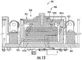
- FIG. 13is a fragmentary, cross-sectional view of the multi-phase active energy absorber module of FIG. 10 taken along the line 13 - 13 of FIG. 11 .
- FIG. 14is a top perspective view of an active energy absorber system according to some embodiments of the invention.
- FIG. 15is an exploded, top perspective view of an active energy absorber module according to some embodiments of the invention and forming a part of the active energy absorber system of FIG. 14 .
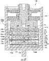
- FIG. 16is a cross-sectional view of the active energy absorber module of FIG. 15 taken along the line 16 - 16 of FIG. 14 .
- FIG. 17is a cross-sectional view of an active energy absorber module according to further embodiments of the invention.
- FIG. 18is a top perspective view of a trigger module forming a part of the active energy absorber module of FIG. 17 .
- FIG. 19is a cross-sectional view of an active energy absorber module according to further embodiments of the invention.
- FIG. 20is a top perspective view of an active energy absorber module according to further embodiments of the invention.
- FIG. 21is a cross-sectional view of the active energy absorber module of FIG. 20 taken along the line 21 - 21 of FIG. 20 .
- FIG. 22is an exploded, top perspective view of a coil assembly forming a part of the active energy absorber module of FIG. 20 .
- FIG. 23is a bottom perspective view of a casing forming a part of the coil assembly of FIG. 22 .
- FIG. 24is a cross-sectional view of an active energy absorber module according to further embodiments of the invention.
- FIG. 25is an exploded, top perspective view of an active component subassembly forming a part of the active energy absorber module of FIG. 24 .
- FIG. 26is a schematic block diagram illustrating a device for active overvoltage protection according to some embodiments of the present invention.
- FIG. 27is a cross-sectional view of an active energy absorber according to further embodiments of the invention.
- FIG. 28is an exploded, perspective view of the active energy absorber of FIG. 27 .
- FIG. 29is a cross-sectional view of an active energy absorber according to further embodiments of the invention.
- FIG. 30is a cross-sectional view of an active energy absorber according to some embodiments of the invention.
- FIG. 31is a schematic block diagram illustrating a device for active overvoltage protection according to some embodiments of the invention.
- FIG. 32is a cross-sectional view of an active energy absorber according to some embodiments of the invention.
- spatially relative termssuch as “under”, “below”, “lower”, “over”, “upper” and the like, may be used herein for ease of description to describe one element or feature's relationship to another element(s) or feature(s) as illustrated in the figures. It will be understood that the spatially relative terms are intended to encompass different orientations of the device in use or operation in addition to the orientation depicted in the figures. For example, if the device in the figures is turned over, elements described as “under” or “beneath” other elements or features would then be oriented “over” the other elements or features. Thus, the exemplary term “under” can encompass both an orientation of over and under. The device may be otherwise oriented (rotated 90 degrees or at other orientations) and the spatially relative descriptors used herein interpreted accordingly.
- types of circuits for providing protection against transient overvoltages, temporary overvoltages and surge/lightning currentmay include varistors that may be directly connected directly between the power lines.
- the difference between a standard varistor used for the protection against transient overvoltages and surge currents and a varistor used for the protection against temporary overvoltages,may be that the second type may be in a conducting mode for a long period of time (in the range of 100 to 300 ms or even more) for a current that may range between a few Amperes and several thousand Amperes, while the first type may be in a conducting mode for a very limited period of time (in the range of few ⁇ s to up to 5 ms) for a current that may range between a few hundred Amperes and over 100 kA.
- the varistorswhen used for the protection against temporary overvoltages they may conduct a significant current from the power source in an effort to clamp the overvoltage that is generated by the power source. As such, they may be required to absorb significant amounts of energy for a long duration. Additionally, when such varistors fail, the failure mode may be a low impedance (i.e., short circuit) failure mode at the end of the device life.
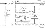
- FIG. 3is a schematic block diagram illustrating a device for active overvoltage protection according to some embodiments of the present invention.
- An active energy absorber 100may be connected between power lines 70 , 72 in an electrical distribution system and/or component.
- the power lines 70 , 72may include power lines and/or a neutral line in a single phase power system or phase lines and/or a neutral line in a multiple phase system (e.g., three phase power system).
- the active energy absorber 100may be connected between two phase or power lines and/or between a phase or power line and a neutral line.
- the active energy absorber 100may provide protection against temporary overvoltages with high energy absorption withstand capabilities and a safe end of life operation.
- an active energy absorber 100may selectively conduct fault current responsive to overvoltage conditions. For example, some embodiments provide that when the active energy absorber 100 is in a conducting mode, that the overvoltage condition may be clamped to a specific voltage by absorbing energy corresponding to the overvoltage fault condition that exceeds the clamped voltage. Some embodiments are directed to providing protection for temporary power system sourced overvoltage conditions that may be sustained for longer periods than transient and/or surge voltages. In use and operation, some embodiments provide that the temporary overvoltages may be clamped to a voltage that is about and/or less than about two times the system operating voltage. For example, in a 220 Volt system, embodiments may set a threshold voltage at about 450 Volts.
- the active energy absorber 100includes an overvoltage protection module 101 that includes two thyristors 102 , 104 that are connected in anti-parallel with one another.
- the thyristors 102 , 104 of the overvoltage protection module 101may be connected in series with a varistor 106 .
- the series circuit including the varistor 106 and the overvoltage protection module 101may be connected between any two of the power lines and the neutral line 70 , 72 .
- the active energy absorber 100includes a trigger circuit 110 that is connected to the power/neutral lines 70 , 72 and to the overvoltage protection module 101 .
- the trigger circuit 110may be configured to provide control signals to the overvoltage protection module 101 responsive to detecting a temporary overvoltage condition across the power/neutral lines 70 , 72 .
- the trigger circuit 110may generate signals to one or both of the thyristors 102 , 104 to turn on (i.e., become a low resistance current conducting path).
- the varistor 106may absorb electrical energy to clamp the voltage between the power lines 70 , 72 to a clamping voltage that may correspond to the threshold voltage.
- the peak voltagemay be 336V.
- the use of a varistor 106 with a Maximum Continuous Operating Voltage (MCOV) of 250V AC as close as possible to the nominal voltagemay be used such that during normal conditions the MOV 106 will not conduct any current.
- MCOVMaximum Continuous Operating Voltage
- a voltage protection levelof around 1000V.
- the trigger circuitwill trigger one of the thyristors 102 , 104 , according to the AC voltage polarity. Once each one of the thyristors 102 , 104 are turned on, the MOV 106 may start conducting heavily in an effort to clamp the voltage.
- the MOV 106may start becoming increasingly resistive and may start reducing the current flow.
- the MOV 106may conduct a very small leakage current (e.g., about 1 mA) at 336V.
- a very small leakage currente.g., about 1 mA
- the current through the thyristors 102 , 104may be reduced to very low values and thus may turn off, for example, thyristors will typically be in a conduction mode only when there is a current flow through them above a certain level, such as, for example, around 200 mA.
- varistors 106 with lower MCOVi.e. thinner varistor disks
- the varistormay have a MCOV of 150V AC instead of 250V AC.
- the fault current corresponding to an overvoltage conditionmay exceed the energy absorption capacity of a single varistor 106 .
- the capacity of a varistor 106may be increased by using multiple varistors 106 that are arranged in parallel with one another. Some embodiments provide that the multiple parallel varistors 106 may be configured in a single device.
- an inductance 120may be provided in one of the lines 70 , 72 to protect thyristors 102 , 104 against a substantially instantaneous change in current (di/dt) in the case of surge events when the thyristors 102 , 104 are self triggered during transient overvoltage events or surge currents due to the dV/dt that the thyristors 102 , 104 will be exposed to.
- this inductance 120may also be considered as part of the power system (cable length, transformers etc.) Some embodiments provide that the inductance 120 may be added to the line 70 , 72 .
- the power distribution system/deviceis an alternating current (AC) system/device.
- the anti-parallel thyristors 102 , 104may be alternatively activated to correspond to different portions of the voltage waveform. For example, in the event of an overvoltage condition during the positive half of the voltage waveform, the second thyristor 104 may be turned on to become conducting as long as the voltage in that half of the waveform remains above a voltage threshold. Once the voltage in that portion of the cycle drops below the threshold voltage, the varistor 106 may cease to conduct because the voltage is sufficiently low and the thyristor 104 may be turned off.
- ACalternating current
- the thyristor 102may be turned on to become conducting as long as the voltage in that half of the waveform is greater than the voltage threshold in the negative direction.
- the active energy absorber 100 described abovemay protect against temporary overvoltages having a slow rise time of the voltage. However, the active energy absorber 100 may not provide sufficient protection during surge events and transient overvoltages.
- the device for active overvoltage protectionmay further include a surge protective device (SPD) 130 that may connected to the power lines 70 , 72 in parallel with the active energy absorber 100 .
- the SPD 130may be configured to protect equipment that is connected thereto during an overvoltage condition by conducting a limited amount of current that corresponds to the surge or transient overvoltage condition.
- an SPD 130may be used in circuits where there are threats of transient overvoltages and surge currents because during such events, there will be an overvoltage, as well as a high rate of rise of voltage, applied on the thyristors 102 , 104 for a period of at least a few ⁇ s. This may result because the response time of the trigger circuit 110 that will trigger the thyristors 102 , 104 and connect the varistor 106 to the power lines 70 , 72 to clamp the overvoltage may take longer than the few ⁇ s. As such, the overvoltage that may be applied for a few ⁇ s may damage the thyristors 102 , 104 if such overvoltage exceeds the maximum operating voltage of the thyristors 102 , 104 .
- the device for active overvoltage protection including an active energy absorber 100 described hereinmay be implemented a device using discrete components for each of the parts composing the circuit, i.e. the coil, the thyristors and the one or more varistors in parallel. Some embodiments provide that the device for active overvoltage protection including an active energy absorber described herein may be implemented as an energy absorber as described above.
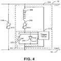
- FIG. 4is a schematic block diagram illustrating a device for active overvoltage protection according to some embodiments of the present invention.
- the device for active overvoltage protectionincludes an SPD 230 and an active energy absorber 200 that includes a varistor 206 , trigger circuit 210 , overvoltage protection module 201 including thyristors 202 , 204 that are similar to the SPD 130 and active energy absorber 100 that includes a varistor 106 , trigger circuit 110 , overvoltage protection module 101 including thyristors 102 , 104 discussed above regarding FIG. 3 . As such, discussion of these components will be omitted for brevity.
- the device of FIG. 4provides that the inductor 208 is a component of the active energy absorber 200 .
- the inductance 208may be connected in series with the series circuit including the varistor 206 and the anti-parallel thyristors 202 , 204 of the overvoltage protection module 201 .
- FIG. 5is a schematic block diagram illustrating a device for active overvoltage protection according to some embodiments of the present invention.
- the device for active overvoltage protectionincludes an SPD 330 , inductance 320 , and an active energy absorber 300 that includes a varistor 306 , trigger circuit 310 , overvoltage protection module 301 including thyristors 302 , 304 that are similar to the SPD 130 , inductance 120 , and active energy absorber 100 that includes a varistor 106 , trigger circuit 110 , overvoltage protection module 101 including thyristors 102 , 104 discussed above regarding FIG. 3 . As such, discussion of these components will be omitted for brevity.
- the active energy absorber 300may include a snubber circuit 312 that is connected in parallel with the overvoltage protection module 301 .
- the snubber circuit 312includes a resistor 316 and a capacitor 314 that are connected in series with one another.
- the snubber circuit 312 used in parallel to the thyristors 302 , 304may reduce and/or eliminate self triggering of the thyristors 302 , 304 during surge events and/or transient overvoltage events. In such cases, the thyristors 302 , 304 may only be triggered by the trigger circuit 310 that is reacting to temporary overvoltage events only. In some embodiments, the inductance 320 may be omitted as the thyristors 302 , 304 may not be expected to conduct surge currents.
- FIG. 6is a schematic block diagram illustrating a device for active overvoltage protection according to some embodiments of the present invention.
- An active energy absorber 400may be connected between power lines 70 , 72 in an electrical distribution system and/or component.
- the power lines 70 , 72may include power lines and/or a neutral line in a single phase power system or phase lines and/or a neutral line in a multiple phase system (e.g., three phase power system).
- the active energy absorber 400may be connected between two phase or power lines and/or between a phase or power line and a neutral line.
- an active energy absorber 400may selectively conduct fault current responsive to overvoltage conditions. For example, some embodiments provide that when the active energy absorber 400 is in a conducting mode, that the overvoltage condition may be clamped to a specific voltage by absorbing energy corresponding to the overvoltage fault condition that exceeds the clamped voltage. Some embodiments are directed to providing protection for temporary power system sourced overvoltage conditions that may be sustained for longer periods than transient and/or surge voltages.
- the active energy absorber 400includes a trigger circuit 410 that may be similar to trigger circuit 110 as discussed above regarding FIG. 3 . As such, additional description thereof will be omitted.
- the active energy absorber 400may include a first thyristor 404 including a first anode that is connected to a first power line 70 , a first cathode and a first gate and a varistor 406 that is connected to the anode and the cathode of the first thyristor 404 .
- the first thyristor 404 and the first varistor 406may be connected in parallel with one another and each be connected to the first power line 70 .
- the active energy absorber 400may include a second thyristor 402 that includes a second anode that is connected to a second power line 72 , a second cathode that is connected to the cathode of the first thyristor 404 , and a second gate.
- a second varistor 408is connected to the anode and the cathode of the second thyristor 402 .
- the second thyristor 402 and the second varistor 408may be connected in parallel with one another and each be connected to the second power line 72 .
- the electrical circuit of the active energy absorber 400may include the SPD functionality. As such, some embodiments provide that the active energy absorber 400 may be used without an additional and/or external SPD.
- the thyristors 402 , 404may be self triggered due to their internal parasitic capacitance between the gate and the anode and the gate and the cathode. According to convention, this parasitic capacitance may be made by the manufacturers to be as low as possible in order to avoid the self triggering of the thyristors 402 , 404 in surge events and transient overvoltage events. However, in the current application, the parasitic capacitance may be higher, which may improve the ease of manufacture. In this regard, the device may demonstrate improved sensitivity to triggering during surge events and transient overvoltage events.
- the voltagemay not reach very high values before the thyristor 402 , 404 is triggered and the voltage is clamped at the protection level of the varistor 406 , 408 .
- the devicemay consistently clamp at the voltage level of a single varistor 406 , 408 , regardless of whether the event is a temporary overvoltage, a surge current or a transient overvoltage.
- the active energy absorber 400may not use a snubber circuit as this circuit may avoid a false trigger of the thyristor due to high dV/dt during surge events or transient overvoltages. Instead, the ability of the thyristors 402 , 404 to self trigger may clamp the voltage through a single varistor.
- an inductance 420may be optionally used to reduce the di/dt through the thyristors 402 , 404 when they conduct a surge current.
- the power lines 70 , 72themselves have significant inductance due to their length, the size of the cables and any transformer installed upstream to the device.
- adding inductance 420 between the power line 70 and the devicemay result in increasing the protection level (clamping voltage) that the equipment will experience during surge events and transient overvoltages.
- an additional in-line modulecould be added to increase the overall inductance of the power line.
- Some embodimentsprovide that since two varistors are used in the same device, the energy absorption can be shared between them during conduction.
- this devicemay provide stand-alone self-triggered operation that can be connected in a power system between two lines and provide protection against temporary overvoltage, transient overvoltage and/or surge/lightning currents.
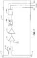
- FIG. 7is a schematic block diagram illustrating a trigger device that may be used in any of the devices described with reference to FIGS. 3-6 according to some embodiments of the present invention.
- the trigger device 510may include a rectifier 512 that is configured to receive AC line voltage from the power lines 70 , 72 and convert the AC line voltage to a DC output voltage that is a voltage level signal which corresponds to the AC line voltage.
- a comparison circuit 514may receive the voltage level signal and a voltage reference signal Vref. The output of the comparison circuit 514 may be based on the comparison between the voltage level signal and the voltage reference signal Vref.
- the output of the comparison circuit 514may correspond to normal operating voltage levels on the power lines 70 , 72 .
- the output of the comparison circuitmay change states to indicate that an overvoltage condition exists.
- the output of the comparison circuit 514may be received by one or more signal driver circuits 516 that may amplify, invert and/or stabilize the output state of the comparison circuit 514 .
- an optical isolation circuit 518 that receives an input corresponding to the output of the comparison circuit 514may provide electrical isolation between the comparison circuit 514 and a gate trigger circuit 520 that is configured to generate one or more gate trigger signals if the output corresponding to the comparison circuit indicates an overvoltage condition on the power lines 70 , 72 .
- the gate trigger signal(s)may be received by the overvoltage protection module and may cause the overvoltage protection module to conduct current corresponding to the temporary overvoltage condition. For example, gate trigger signals may be received at each of the two thyristors in the active energy absorber embodiments disclosed herein.
- operationsmay include sensing, using a trigger circuit, an overvoltage condition on a power line (block 810 ).
- the power linemay be a phase power line in a multiple phase power system and/or a single phase power line.
- the overvoltage conditionmay be relative to another power line and/or a neutral line.
- the overvoltage conditionmay be a temporary overvoltage system that may last for a significant period of time, such as, for example, 100 ms to 300 ms or more, in contrast with a surge or transient overvoltage event that may have a much shorter duration.
- operationsmay include switching an overvoltage protection device into a conducting mode (block 820 ).
- the overvoltage protection deviceWhen the overvoltage protection device is switched into a conducting mode, the voltage on the power line is clamped to a voltage limit that corresponds to an operating voltage of the power circuit.
- the voltage limitmay be clamped to some multiple of the operating voltage of the power circuit.
- the multiplemay be in a range from 1.4 to 3.0 such that the voltage is clamped to a voltage that is 1.4 to 3.9 times the system operating voltage.
- the multiplemay be around 2 such that the voltage is clamped to a voltage that is around 2 times the system operating voltage.
- the overvoltage protection deviceincludes one or more thyristors that are in series with an SPD and that are switched into a conducting mode. In such embodiments, the SPD may serve to clamp the voltage by absorbing the energy corresponding to the fault current.
- operationsmay include sensing that the overvoltage condition on the power line is not present (block 830 ). This can be done following the feature of the thyristor in which it is disconnected from the power line when the conducted current drops below a certain threshold, such as, for example, around 200 mA. As the voltage drops, at some point the voltage will reach a level below which the MOV connected in series to the thyristor will only allow a current of less than about 200 mA to be conducted therethrough. This may also signify that the TOV condition is elapsed. In response to detecting that the overvoltage condition is not present, the overvoltage protection device may be switched into a non-conducting mode (block 840 ).
- the power circuitis an alternating current (AC) power circuit and sensing the overvoltage condition may correspond to a first portion of a voltage waveform and that, after switching the overvoltage protection into a non-conducting mode, the trigger circuit may sense another overvoltage condition corresponding to a second portion of the voltage waveform.
- the overvoltage protection devicemay switch into a conducting mode that is configured to clamp the voltage to a second portion voltage waveform voltage limit.
- some embodimentsprovide that switching the overvoltage protection device during the first portion of the voltage waveform is performed using a first thyristor and switching the overvoltage protection device during the second portion of the voltage waveform is performed using a second thyristor that is connected in anti-parallel with the first thyristor.
- FIG. 9is a graph of voltage versus time in an overvoltage condition based on the overvoltage protection of some embodiments of the present invention.
- the overvoltage conditionbegins at time T 1 .
- a voltage thresholdV-threshold
- the overvoltage protectionturns on to become conducting and the voltage is clamped to a clamp voltage (V-clamp).
- V-clampvoltage threshold
- the overvoltage protectionreduces from the clamp voltage V-clamp to the operating voltage V-operating until the voltage reduces to a level below the clamp voltage.
- the overvoltage protectionturns off and thus ceases to conduct current at time T 3 .
- some embodimentsprovide that the overvoltage protection turns off when the given trigger fault current reaches about 220 mA, however, the given trigger fault current may be more or less than 220 mA.
- the illustrated embodimentis a multi-phase active energy absorber module 901 that is a three phase implementation and therefore includes three active energy absorber subassemblies 900 each corresponding to one of the active energy absorbers 100 of FIG. 3 . That is, the active energy absorber 100 of each phase is embodied in a respective subassembly 900 .
- Each subassembly 900includes an MOV module 920 (corresponding to the MOV 106 ), two thyristors 102 , 104 (corresponding to the thyristors 102 , 104 of FIG.
- Each subassembly 900is electrically connected to and mechanical mounted on an electrically conductive neutral plate 903 and includes a respective line terminal 902 .
- a neutral terminal 904is also connected to the neutral plate 903 .
- the trigger circuit 930is provided on a PCB 932 .
- the subassemblies 900 and the neutral plate 903are contained in a module housing 906 .
- each MOV module 920may be constructed as disclosed in one or more of U.S. Pat. No. 6,038,119 to Atkins et al. and U.S. Pat. No. 6,430,020 to Atkins et al., the disclosures of which are incorporated herein by reference.
- each MOV module 920includes a metal housing electrode 922 , a metal piston electrode 924 , and plurality of varistor wafers 926 stacked between a head 924 A of the electrode 924 and an electrode end wall 922 A of the housing 922 .
- the varistor wafers 926are connected in electrical parallel between the inner faces of the head 924 A and the end wall 922 A by electrically conductive interconnect members 928 .
- the electrodes 922 and 924collectively form a chamber 921 A within which the varistors 926 are contained and encapsulated.
- each subassembly 900is further provided with an inductor corresponding to the inductor 208 .
- the electrical circuit of FIG. 6is implemented or packaged as an active energy absorber module including a single integrated device wherein the varistors 106 and thyristors 102 , 104 are encapsulated in a sturdy housing assembly.
- an active energy absorber system 1001according to embodiments of the invention is shown therein.
- the system 1001includes a modular active energy absorber unit or module 1000 according to embodiments of the invention and an external trigger circuit 1002 .
- One system 1001may be used for each of the active energy absorbers 400 in FIG. 6 .
- the trigger circuit 1002may be any suitable device incorporating the trigger circuit 410 of FIG. 6 .
- the trigger circuit 1002may be packaged in a protective housing.
- the active energy absorber module unit 1000has a lengthwise axis A-A ( FIG. 16 ).
- the active energy absorber module 1000includes a first electrode or housing 1022 , a piston-shaped second electrode 1024 , four spring washers 1028 E, a flat washer 1028 D, an insulating ring member 1028 C, three O-rings 1030 A-C, an end cap 1028 A, a retention clip 1028 B, a meltable member 1032 , an insulator sleeve 1034 , and a cable gland 1036 .
- the active energy absorber module unitfurther includes an active component subassembly 1040 including three internal interconnect members 1054 , 1056 , 1058 , two varistor members 1042 , 1044 , two thyristors 1046 , 1048 , two contact plates 1050 , 1052 , two gate connectors 1062 D, and two signal cables 1062 A-B.
- an active component subassembly 1040including three internal interconnect members 1054 , 1056 , 1058 , two varistor members 1042 , 1044 , two thyristors 1046 , 1048 , two contact plates 1050 , 1052 , two gate connectors 1062 D, and two signal cables 1062 A-B.
- the components 1022 , 1024 , 1028 A-Ccollectively form a housing assembly defining a sealed, enclosed chamber 1026 .
- the components 1022 , 1024 , 1028 A-E, 1032 and 1040are disposed axially between the housing and the electrode along the lengthwise axis A-A, in the enclosed chamber 1026 .
- the housing 1022has an end electrode wall 1022 A and an integral cylindrical sidewall 1022 B extending from the electrode wall 1022 A.
- the sidewall 1022 B and the electrode wall 1022 Aform a chamber or cavity 1022 C communicating with an opening 1022 D.
- a threaded post 1022 Eprojects axially outwardly from the electrode wall 1022 A.
- a wire aperture or port 1022 Fextends through the side wall 1022 B.
- the electrode wall 1022 Ahas an inwardly facing, substantially planar contact surface 1022 G.
- An annular clip slot 1022 His formed in the inner surface of the sidewall 1022 B.
- the housing 1022is formed of aluminum. However, any suitable electrically conductive metal may be used.
- the housing 1022is unitary and, in some embodiments, monolithic.
- the housing 1022 as illustratedis cylindrically shaped, but may be shaped differently.
- the inner electrode 1024has a head 1024 A disposed in the cavity 1022 C and an integral shaft 1022 B that projects outwardly through the opening 1022 D.
- the head 1024 Ahas a substantially planar contact surface 1024 C that faces the contact surface 1022 G of the electrode wall 1022 A.
- a pair of integral, annular, axially spaced apart flanges 1024 Dextend radially outwardly from the shaft 1024 B and define an annular, sidewardly opening groove 1024 E therebetween.
- a threaded bore 1024 Fis formed in the end of the shaft 1024 B to receive a bolt for securing the electrode 1024 to a busbar, for example.
- An annular, sidewardly opening groove 1024 Gis defined in the shaft 1024 B.
- the electrode 1024is formed of aluminum. However, any suitable electrically conductive metal may be used. According to some embodiments, the electrode 1024 is unitary and, in some embodiments, monolithic.
- the electrodes 1022 , 1024 , the insulating ring 1028 C and the end cap 1028 Acollectively define an enclosed chamber 1026 containing the meltable member 1032 and the active component subassembly 1040 .
- An annular gapis defined radially between the head 1024 A and the nearest adjacent surface of the sidewall 1022 B. According to some embodiments, the gap has a radial width in the range of from about 3 to 10 mm.
- the meltable member 1032is annular and is mounted on the electrode 1024 in the groove 1024 E.
- the meltable member 1032is spaced apart from the sidewall 1022 B a distance sufficient to electrically isolate the meltable member 1032 from the sidewall 1022 B.
- the meltable member 1032is formed of a heat-meltable, electrically conductive material. According to some embodiments, the meltable member 1032 is formed of metal. According to some embodiments, the meltable member 1032 is formed of an electrically conductive metal alloy. According to some embodiments, the meltable member 1032 is formed of a metal alloy from the group consisting of aluminum alloy, zinc alloy, and/or tin alloy. However, any suitable electrically conductive metal may be used.
- the meltable member 1032is selected such that its melting point is greater than a prescribed maximum standard operating temperature.
- the maximum standard operating temperaturemay be the greatest temperature expected in the meltable member 1032 during normal operation (including handling overvoltage surges within the designed for range of the system 1001 ) but not during operation which, if left unchecked, would result in thermal runaway.
- the meltable member 1032is formed of a material having a melting point in the range of from about 80 to 160° C. and, according to some embodiments, in the range of from about 130 to 150° C.
- the melting point of the meltable member 1032is at least 20° C. less than the melting points of the housing 1022 and the electrode 1024 and, according to some embodiments, at least 40° C. less than the melting points of those components.
- the meltable member 1032has an electrical conductivity in the range of from about 0.5 ⁇ 10 6 Siemens/meter (S/m) to 4 ⁇ 10 7 S/m and, according to some embodiments, in the range of from about 1 ⁇ 10 6 S/m to 3 ⁇ 10 6 S/m.
- the two varistors 1042 , 1044 , the two thyristors 1046 , 1048 , the two contact plates 1050 , 1052 , the insulator member 1060 , and the three interconnect members 1054 , 1056 , 1058are axially stacked in the chamber 1026 between the electrode head 1024 and the electrode wall 1022 and form an active component subassembly 1040 .
- the subassembly 1040corresponds to or forms the parts of the electrical circuit shown in FIG.
- the varistor 1042corresponds to the varistor 406
- the varistor 1044corresponds to the varistor 408
- the thyristor 1046corresponds to the thyristor 402
- the thyristor 1048corresponds to the thyristor 404
- the trigger circuit 1002corresponds to the trigger circuit 410 .
- the interconnect members 1054 , 1056 and the contact plates 1050 , 1052electrically interconnect the varistors 1042 , 1044 , thyristors 1046 , 1048 , and trigger circuit 1002 in the manner represented in FIG. 6 .
- each varistor member 1042 , 1044has first and second opposed, substantially planar contact surfaces 1043 .
- each varistor member 1042 , 1044is a varistor wafer (i.e., is wafer- or disk-shaped).
- varistor members 1042 , 1044may be formed in other shapes.
- the thickness and the diameter of the varistor wafers 1042 , 1044will depend on the varistor characteristics desired for the particular application.
- each varistor wafer 1042 , 1044has a diameter to thickness ratio of at least 3.
- the thickness of each varistor wafer 1042 , 1044is in the range of from about 1.5 to 15 mm.
- the varistor wafers 1042 , 1044may include a wafer of varistor material coated on either side with a conductive coating so that the exposed surfaces of the coatings serve as the contact surfaces.
- the coatingscan be formed of aluminum, copper or silver, for example.
- the varistor materialmay be any suitable material conventionally used for varistors, namely, a material exhibiting a nonlinear resistance characteristic with applied voltage. Preferably, the resistance becomes very low when a prescribed voltage is exceeded.
- the varistor materialmay be a doped metal oxide or silicon carbide, for example. Suitable metal oxides include zinc oxide compounds.
- the two thyristors 1046 , 1048may be constructed in the same or similar manner.
- the thyristors 1046 , 1048are wafer- or disk-shaped.
- each thyristor 1046 , 1048has a diameter to thickness ratio of at least 15.
- the thickness of each thyristor 1046 , 1048is in the range of from about 1.5 to 10 mm.
- Each thyristor 1046 , 1048includes a body 1045 A and an anode 1045 C and a cathode 1045 B on axially opposed sides of the body 1045 A.
- the anode 1045 C and the cathode 1045 Bhave substantially planar contact surfaces.
- Each thyristor 1046 , 1048further includes a gate or control terminal 1045 F ( FIG. 15 ).
- the gate terminal 1045 Fis located in the center of the same plate as the cathode 1045 B and is surrounded by (but electrically insulated from) the cathode 1045 B.
- An annular insulator 1045 Gis axially interposed between the anode 1045 C and the cathode 1045 B and electrically insulates the anode 1045 C from the cathode 1045 B.
- Suitable thyristors for the thyristors 1046 , 1048may be constructed as disclosed in, for example, U.S. Pat. No. 4,956,696 to Hoppe et al., the disclosure of which is incorporated herein by reference.
- the cable gland 1036is affixed in the wire port 1022 F.
- the signal cables 1062 A, 1062 Bextend through the wire port 1022 F and the cable gland 1036 and into the chamber 1026 .
- the cable gland 1036is secured in the wire port 1022 F.
- the cable gland 1036serves to mechanically retain or secure the wires in the port 1022 F (providing strain relief) and to fully seal, plug or close the bore in the side wall 1022 B (e.g., hermetically).
- the signal cable 1062 Aincludes a gate wire 1762 GA electrically terminated at the control terminal 1045 F of the thyristor 1046 .
- the signal cable 1062 Aalso includes a reference wire electrically terminated at the cathode 1045 B of the thyristor 1046 .
- the signal cable 1062 Bincludes a gate wire 1762 GB electrically terminated at the control terminal 1045 F of the thyristor 1048 .
- the signal cable 1062 Balso includes a reference wire electrically terminated at the cathode 1045 B of the thyristor 1048 .
- the gate wires 1062 GA, 1062 GB of the cables 1062 A, 1062 Bare terminated and electrically and mechanically connected to the control terminals 1045 F of the thyristors 1046 , 1048 by the gate connectors 1062 D.
- Each gate connector 1062 Dmay include a spring 1062 E that loads or biases the gate connector 1062 D against the associated control terminal 1045 F.
- the reference wires of the cables 1062 A, 1062 Bmay be thin wires or foils, for example, interposed between each cathode 1045 B and the opposing face of the adjacent contact plate 1050 , 1052 .
- the reference wireis connected (e.g., by soldering) to a thin metal sheet (e.g., with a thickness in the range of from about 0.1 mm to 1 mm; not shown for simplicity) that is positioned between the cathode 1045 B and the contact plate 1050 , or 1052 .
- the triggering of each thyristor 1046 , 1048is done through the two wires (i.e., a gate wire and a reference wire) of the respective signal cable 1062 A, 1062 B.
- the reference wires of the cables 1062 A and 1062 Bmay be mechanically terminated and electrically connected (e.g., by soldering) to the bridge portions 1057 B of the interconnect members 1054 and 1056 , respectively, as described below with reference to FIG. 27 , for example.
- the reference wire of the cable 1062 Awould be electrically connected to its cathode 1045 B through the interconnect member 1054 and the contact plate 1050
- the reference wire of the cable 1062 Bwould be connected to its cathode 1045 B through the interconnect member 1056 and the contact plate 1052 .
- the contact plates 1050 , 1052are electrically conductive. Each contact plate 1050 , 1052 is disk-shaped and has opposed contact surfaces 1051 A. Each contact plate 1050 , 1052 also has formed therein a central through hole 1051 B and a slot 1051 C extending radially from the through hole 1051 B to the outer periphery of the contact plate 1050 , 1052 . Each control or gate wire of the signal cables 1062 A, 1062 B is routed through the slot 1051 C of a corresponding contact plate 1050 , 1052 and each associated gate connector 1062 D is seated in the through hole 1051 B of the corresponding contact plate 1050 , 1052 .
- the contact plates 1050 , 1052are formed of copper alloy. However, any suitable electrically conductive metal may be used. According to some embodiments, the contact plates 1050 , 1052 are unitary and, in some embodiments, monolithic.
- the interconnect members 1054 , 1056 , 1058are electrically conductive. Each interconnect member 1054 , 1056 , 1058 includes a pair of axially spaced apart, disk-shaped contact portions 1057 A joined by a bridge portion 1057 B.
- the interconnect members 1054 , 1056 , 1058are formed of copper. However, any suitable electrically conductive metal may be used. According to some embodiments, the interconnect members 1054 , 1056 , 1058 are unitary and, in some embodiments, monolithic.
- the insulator member 1060may be a relatively thin layer or disk of an electrically insulating material. In some embodiments, the insulator member 1060 has a thickness in the range of from about 1 to 10 mm.
- the insulator member 1060is formed of a hard, high temperature polymer and, in some embodiments, a hard, high temperature thermoplastic. In some embodiments, the insulator member 1060 is formed of mica.
- the insulator member 1060is formed of a material having a melting point greater than the melting point of the meltable member 1032 . According to some embodiments, the insulator member 1060 is formed of a material having a melting point in the range of from about 120 to 200° C.
- the insulator member 1060 materialcan withstand a voltage of 25 kV per mm of thickness.
- the insulator member 1060has a thickness in the range of from about 0.1 to 10 mm.
- the insulator sleeve 1034is tubular and generally cylindrical. According to some embodiments, the insulator sleeve 1034 is formed of a high temperature polymer and, in some embodiments, a high temperature thermoplastic. In some embodiments, the insulator sleeve 1034 is formed of polyetherimide (PEI), such as ULTEMTM thermoplastic available from SABIC of Saudi Arabia. In some embodiments, the membrane 1060 is formed of non-reinforced polyetherimide.
- PEIpolyetherimide
- the membrane 1060is formed of non-reinforced polyetherimide.
- the insulator sleeve 1034is formed of a material having a melting point greater than the melting point of the meltable member 1032 . According to some embodiments, the insulator sleeve 1034 is formed of a material having a melting point in the range of from about 120 to 200° C.
- the insulator sleeve 1034 materialcan withstand a voltage of 25 kV per mm of thickness.
- the insulator sleeve 1034has a thickness in the range of from about 0.1 to 2 mm.
- the spring washers 1028 Esurround the shaft 1024 B. Each spring washer 1028 E includes a hole that receives the shaft 1024 B. The lowermost spring washer 1028 E abuts the top face of the head 1024 A. According to some embodiments, the clearance between the spring washer hole and the shaft 1024 B is in the range of from about 0.015 to 0.035 inch.
- the spring washers 1028 Emay be formed of a resilient material. According to some embodiments and as illustrated, the spring washers 1028 E are Belleville washers formed of spring steel. While two spring washers 1028 E are shown, more or fewer may be used. The springs may be provided in a different stack arrangement such as in series, parallel, or series and parallel.
- the flat metal washer 1028 Dis interposed between the uppermost spring washer 1028 E and the insulator ring 1028 C with the shaft 1024 B extending through a hole formed in the washer 1028 D.
- the washer 1028 Dserves to distribute the mechanical load of the upper spring washer 1028 E to prevent the spring washer 1028 E from cutting into the insulator ring 1028 C.
- the insulator ring 1028 Coverlies and abuts the washer 1028 D.
- the insulator ring 1028 Chas a main body ring and a cylindrical upper flange or collar extending upwardly from the main body ring.
- a holereceives the shaft 1024 B.
- the clearance between the hole and the shaft 1024 Bis in range of from about 0.025 to 0.065 inch.
- An upwardly and outwardly opening peripheral grooveis formed in the top corner of the main body ring.
- the insulator ring 1028 Cis preferably formed of a dielectric or electrically insulating material having high melting and combustion temperatures.
- the insulator ring 1028 Cmay be formed of polycarbonate, ceramic or a high temperature polymer, for example.
- the end cap 1028 Aoverlies and abuts the insulator ring 1028 C.
- the end cap 1028 Ahas a hole that receives the shaft 1024 B. According to some embodiments, the clearance between the hole and the shaft 1024 B is in the range of from about 0.1 to 0.2 inch.
- the end cap 1028 Amay be formed of aluminum, for example.
- the clip 1028 Bis resilient and truncated ring shaped.
- the clip 1028 Bis partly received in the slot 1022 H and partly extends radially inwardly from the inner wall of the housing 1022 to limit outward axial displacement of the end cap 1028 A.
- the clip 1028 Bmay be formed of spring steel.
- the O-ring 1030 Bis positioned in the groove 1024 G so that it is captured between the shaft 1024 B and the insulator ring 1028 C.
- the O-ring 1030 Ais positioned in the groove in the insulator ring 1028 C such that it is captured between the insulating member 1028 C and the sidewall 1022 B.
- the O-ring 1030 Cis positioned in the groove 102411 to seal with the insulator ring 1028 C. When installed, the O-rings 1030 A-C are compressed so that they are biased against and form a seal between the adjacent interfacing surfaces.
- byproductssuch as hot gases and fragments from the thyristors 1046 , 1048 or varistors 1042 , 1044 may fill or scatter into the cavity chamber 1026 . These byproducts may be constrained or prevented by the O-rings 1030 A-C from escaping the active energy absorber module 1000 through the housing opening 1022 D.
- the O-rings 1030 A-Cmay be formed of the same or different materials. According to some embodiments, the O-rings 1030 A-C are formed of a resilient material, such as an elastomer. According to some embodiments, the O-rings 1030 A-C are formed of rubber. The O-rings 1030 A-C may be formed of a fluorocarbon rubber such as VITONTM available from DuPont. Other rubbers such as butyl rubber may also be used. According to some embodiments, the rubber has a durometer of between about 60 and 100 Shore A.
- the electrode head 1024 A and the housing end wall 1022 Aare persistently biased or loaded against the active component subassembly 1040 along a load or clamping axis C-C ( FIG. 16 ) in directions F to ensure firm and uniform engagement between the above-identified interfacing contact surfaces.
- This aspect of the unit 1000may be appreciated by considering a method according to the present invention for assembling the unit 1000 , as described below.
- the clamping axis C-Cis substantially coincident with the axis A-A ( FIG. 16 ).
- the signal cables 1062 A-Bare secured in the bore of the cable gland 1036 .
- the cable gland 1036is secured in the wire port 1022 F (e.g., using adhesive).
- the cables 1062 A-Bare connected to the terminals 1045 F, 1045 G.
- the components 1042 , 1044 , 1046 , 1048 , 1050 , 1052 , 1054 , 1056 , 1058 , 1060are assembled to form the active component subassembly 1040 ( FIG. 16 ).
- the subassembly 1040is placed in the cavity 1022 C such that the lower contact surface or portion 1051 A of the interconnect member 1056 engages the contact surface 1022 G of the end wall 1022 A.
- the O-rings 1030 A-Care installed in their respective grooves.
- the head 1024 Ais inserted into the cavity 1022 C such that the contact surface 1024 C engages the upper contact surface or portion 1051 A of the interconnect member 1054 .
- the spring washers 1028 Eare slid down the shaft 1024 B.
- the washer 1028 D, the insulator ring 1028 C, and the end cap 1028 Aare slid down the shaft 1024 B and over the spring washers 1028 E.
- a jig (not shown) or other suitable deviceis used to force the end cap 1028 A down, in turn deflecting the spring washers 1028 E. While the end cap 1028 A is still under the load of the jig, the clip 1028 B is compressed and inserted into the slot 1022 H. The clip 1028 B is then released and allowed to return to its original diameter, whereupon it partly fills the slot and partly extends radially inward into the cavity from the slot 1022 H.
- the clip 1028 B and the slot 1022 Hthereby serve to maintain the load on the end cap 1028 A to partially deflect the spring washers 1028 E.
- the loading of the end cap 1028 A onto the insulator ring 1028 C and from the insulator ring onto the spring washersis in turn transferred to the head 1024 A.
- the subassembly 1040is sandwiched (clamped) between the head 1024 A and the electrode wall 1022 A.
- the housing 1022 , the electrode 1024 , the insulating member 1028 C, the end cap 1028 A, the clip 1028 B, the O-rings 1030 A-C and the cable gland 1036collectively form a unit housing or housing assembly 1021 containing the components in the chamber 1026 .
- the large, planar contact surfaces of the components 1022 A, 1024 A, 1042 , 1044 , 1046 , 1048 , 1050 , 1052 , 1054can ensure reliable and consistent electrical contact and connection between the components during an overvoltage or surge current event.
- the head 1024 A and the end wall 1022 Aare mechanically loaded against these components to ensure firm and uniform engagement between the mating contact surfaces.
- the active energy absorber module 1000integrates two varistors 1042 , 1044 in electrical parallel in the same modular device, so that energy can be shared between the varistors 1042 , 1044 during electrical conduction.
- the design of the active energy absorber module 1000provides compressive loading of the thyristors 1046 , 1048 in combination with the varistor wafers 1042 , 1044 in a single modular unit.
- the active energy absorber module 1000provides suitable electrical interconnections between the electrodes 1042 , 1044 , thyristors 1046 , 1048 , and varistor wafers 1042 , 1044 , while retaining a compact form factor and providing proper thermal dissipation of energy from the varistors 1042 , 1044 .
- the construction of the active energy absorber module 1000provides a safe failure mode for the device.
- one or more of the varistors 1042 , 1044 and the thyristors 1046 , 1048may be damaged by overheating and may generate arcing inside the housing assembly 1021 .
- the housing assembly 1021can contain the damage (e.g., debris, gases and immediate heat) within the active energy absorber module 1000 , so that the active energy absorber module 1000 fails safely.
- the active energy absorber module 1000can prevent or reduce any damage to adjacent equipment (e.g., switch gear equipment in the cabinet) and harm to personnel. In this manner, the active energy absorber module 1000 can enhance the safety of equipment and personnel.
- the active energy absorber module 1000provides a fail-safe mechanism in response to end of life mode in one of more of the varistors 1042 , 1044 .
- a fault currentwill be conducted between the corresponding line (e.g., Line 1 of FIG. 6 ) and the neutral line.
- a varistorhas an innate nominal clamping voltage VNOM (sometimes referred to as the “breakdown voltage” or simply the “varistor voltage”) at which the varistor begins to conduct current. Below the VNOM, the varistor will not pass current. Above the VNOM, the varistor will conduct a current (i.e., a leakage current or a surge current).
- the VNOM of a varistoris typically specified as the measured voltage across the varistor with a DC current of 1 mA.
- a varistorhas three modes of operation. In a first normal mode (discussed above), up to a nominal voltage, the varistor is practically an electrical insulator. In a second normal mode (also discussed above), when the varistor is subjected to an overvoltage, the varistor temporarily and reversibly becomes an electrical conductor during the overvoltage condition and returns to the first mode thereafter. In a third mode (the so-called end of life mode), the varistor is effectively depleted and becomes a permanent, non-reversible electrical conductor.
- the varistoralso has an innate clamping voltage VC (sometimes referred to as simply the “clamping voltage”).
- the clamping voltage VCis defined as the maximum voltage measured across the varistor when a specified current is applied to the varistor over time according to a standard protocol.
- the varistor wafer 1042 , 1044provides high resistance such that no current flows through the active energy absorber module 1000 as it appears electrically as an open circuit. That is, ordinarily the varistor passes no current.
- an overcurrent surge eventtypically transient; e.g., lightning strike
- an overvoltage condition or eventtypically longer in duration than an overcurrent surge event
- the resistance of the varistor waferdecreases rapidly, allowing current to flow through the active energy absorber module 1000 and create a shunt path for current flow to protect other components of an associated electrical system. Normally, the varistor recovers from these events without significant overheating of the active energy absorber module 1000 .
- Varistorshave multiple failure modes.
- the failure modesinclude: 1) the varistor fails as a short circuit; and 2) the varistor fails as a linear resistance.
- the failure of the varistor to a short circuit or to a linear resistancemay be caused by the conduction of a single or multiple surge currents of sufficient magnitude and duration or by a single or multiple continuous overvoltage events that will drive a sufficient current through the varistor.
- a short circuit failuretypically manifests as a localized pinhole or puncture site (herein, “the failure site”) extending through the thickness of the varistor.
- This failure sitecreates a path for current flow between the two electrodes of a low resistance, but high enough to generate ohmic losses and cause overheating of the device even at low fault currents.
- Sufficiently large fault current through the varistorcan melt the varistor in the region of the failure site and generate an electric arc.
- a varistor failure as a linear resistancewill cause the conduction of a limited current through the varistor that will result in a buildup of heat. This heat buildup may result in catastrophic thermal runaway and the device temperature may exceed a prescribed maximum temperature.
- the maximum allowable temperature for the exterior surfaces of the devicemay be set by code or standard to prevent combustion of adjacent components. If the leakage current is not interrupted at a certain period of time, the overheating will result eventually in the failure of the varistor to a short circuit as defined above.
- the current through the failed varistorcould also be limited by the power system itself (e.g., ground resistance in the system or in photo-voltaic (PV) power source applications where the fault current depends on the power generation capability of the system at the time of the failure) resulting in a progressive build up of temperature, even if the varistor failure is a short circuit.
- the power systemitself
- PVphoto-voltaic
- a thyristormay also fail in a short circuit in a similar manner as the varistor when the energy dissipated on the thyristor exceeds its power dissipation limit, which may be represented by the current squared times the time (i 2 *t). The difference may be that under the same current level conducted, the thyristor may dissipate far less energy so it is unlikely to fail first, if the latter is properly designed and dimensional for specific application.
- the manner of failuremay be very similar to that of a MOV, namely through a low ohmic resistance path or a pinhole that may generate an arc and/or overheating.
- the active energy absorber module 1000may assume an “end of life” mode in which a varistor wafer 1042 , 1044 is depleted in full or in part (i.e., in an “end of life” state), leading to an end of life failure.
- the varistorreaches its end of life, the active energy absorber module 1000 will become substantially a short circuit with a very low but non-zero ohmic resistance.
- a fault currentwill continuously flow through the varistor even in the absence of an overvoltage condition.
- the meltable member 1032can operate as a fail-safe mechanism that by-passes the failed varistor and creates a permanent low-ohmic short circuit between the terminals of the active energy absorber module 1000 in the manner described in U.S. Pat. No. 7,433,169, the disclosure of which is incorporated herein by reference.
- Each thyristor 1046 , 1048can likewise fail with the same or similar failure modes as described herein for the varistors 1042 , 1044 , including failing as a short circuit, and failing as a linear resistance.
- the thyristors 1046 , 1048can likewise assume an “end of life” mode as described for the varistors 1042 , 1044 .
- the thyristors 1046 , 1048will exhibit similar or substantially the same behavior and response as described for the varistors 1042 , 1044 .
- the same by-pass mechanismcan be used inside the same chamber to enable the fail-safe operation of the device 1000 when either a varistor 1042 , 1044 or a thyristor 1046 , 1048 fails.
- the meltable member 1032is adapted and configured to operate as a thermal disconnect to electrically short circuit the current applied to the associated active energy absorber module 1000 around the varistors 1042 , 1044 and the thyristors 1046 , 1048 to prevent or reduce the generation of heat in the varistors and thyristors. In this way, the meltable member 1032 can operate as switch to bypass the varistors 1042 , 1044 and thyristors 1046 , 1048 and prevent overheating and catastrophic failure as described above.
- a fail-safe systemis “triggered” upon occurrence of the conditions necessary to cause the fail-safe system to operate as described to short circuit the electrodes 1022 A, 1024 A.
- the meltable member 1032When heated to a threshold temperature, the meltable member 1032 will flow to bridge and electrically connect the electrodes 1022 A, 1024 A. The meltable member 1032 thereby redirects the current applied to the active energy absorber module 1000 to bypass the varistors 1042 , 1044 and thyristors 1046 , 1048 so that the current induced heating of the varistor or thyristor ceases.
- the meltable member 1032may thereby serve to prevent or inhibit thermal runaway (caused by or generated in a varistor 1042 , 1044 and/or a thyristor 1046 , 1048 ) without requiring that the current through the active energy absorber module 1000 be interrupted.
- the meltable member 1032initially has a first configuration as shown in FIGS. 15 and 16 such that it does not electrically couple the electrode 1024 and the housing 1022 except through the head 1024 A. Upon the occurrence of a heat buildup event, the electrode 1024 is thereby heated. The meltable member 1032 is also heated directly and/or by the electrode 1024 . During normal operation, the temperature in the meltable member 1032 remains below its melting point so that the meltable member 1032 remains in solid form. However, when the temperature of the meltable member 1032 exceeds its melting point, the meltable member 1032 melts (in full or in part) and flows by force of gravity into a second configuration different from the first configuration.
- the meltable member 1032bridges or short circuits the electrode 1024 to the housing 1022 to bypass the varistors 1042 , 1044 and the thyristors 1046 , 1048 . That is, a new direct flow path or paths are provided from the surface of the electrode 1024 to the surface of the housing sidewall 1022 B through the meltable member 1032 . According to some embodiments, at least some of these flow paths do not include the varistor wafers 1042 , 1044 or the thyristors 1046 , 1048 .
- the active energy absorber module 1000is adapted such that when the meltable member 1032 is triggered to short circuit the active energy absorber module 1000 , the conductivity of the active energy absorber module 1000 is at least as great as the conductivity of the feed and exit cables connected to the device.
- an active energy absorber module 1100corresponds to the active energy absorber module 400 of the electrical circuit of FIG. 6 .
- the active energy absorber module 1100is constructed in the same manner as the active energy absorber module 1000 , except that the trigger circuit 1102 is integrated within the active energy absorber module 1100 and encapsulated in the enclosed chamber 1126 of the housing assembly 1121 .
- the active energy absorber module 1100can operate as a stand-alone, self-triggering device that can be connected between two lines and provide protection against overvoltage (temporary and transient) and surge (e.g., lightning) events. Because the trigger circuit 1102 is contained in the housing assembly 1121 , the wire port 1022 F can be eliminated.
- the inner electrode 1124has a two piece construction including a shaft member 1125 threadedly secured to a head member 1127 .
- the trigger circuit 1102is contained in a trigger circuit housing 1170 A.
- the trigger circuit 1102 and the housing 1170 Atogether form a trigger circuit module 1170 .
- the shaft member 1125extends through the housing 1170 A and the trigger circuit module 1170 is captured between the head 1127 and an integral flange 1125 A of the shaft member 1125 .
- a wire assembly 1162 corresponding to the wire assembly 1062electrically connects the trigger circuit 1102 to the thyristors.
- an active energy absorber module 1200is shown therein.
- the active energy absorber module 1200is constructed in the same manner as the active energy absorber module 1100 (including a housing assembly 1221 corresponding to the housing assembly 1021 and a trigger circuit module 1270 and a trigger circuit 1202 encapsulated in the enclosed chamber 1226 ), except that each of leg of the circuit includes three varistor wafers 1242 in parallel.
- This embodimentcan provide higher energy absorption than the active energy absorber module 1000 of FIG. 17 , for example (when the varistors are of the same construction as the varistors).
- an active energy absorber module 1300corresponds to the active energy absorber circuit 400 of the electrical circuit of FIG. 6 except that the unit 1300 further integrates the inductor 420 into the active energy absorber module 1300 .
- the active energy absorber module 1300is constructed in the same manner as the active energy absorber module 1100 (including a housing assembly 1321 corresponding to the housing assembly 1121 , and a trigger circuit module 1370 and a trigger circuit 1302 encapsulated in the chamber 1326 ), except that the active energy absorber module 1300 further includes an integral inductance coil assembly 1380 encapsulated in the cavity 1326 .
- the coil assembly 1380includes a coil 1381 corresponding to the coil 420 of the electrical circuit of FIG. 6 .
- the coil assembly 1380includes an electrically conductive outer coil member 1382 , an electrically conductive inner coil member 1384 , an electrically conductive interface plate 1385 A, coupling fasteners 1385 B, an electrically conductive terminal member or shaft 1386 , an electrical insulator sheet 1385 C, an electrically conductive coupling member 1387 , an electrically insulating casing 1388 , and an electrically insulating outer cover 1389 .
- the coil members 1382 , 1384collectively form the coil 1381 .
- the outer coil member 1382includes a coil body 1382 A, a spirally extending coil strip 1382 B defining a spiral coil channel 1382 C, and a coupling extension 1382 D.
- a threaded bore 1382 Eextends axially through the coil body 1382 A.
- the inner coil member 1384includes a coil body 1384 A, a spirally extending coil strip 1384 B defining a spiral coil channel 1384 C, and a coupling extension 1384 D.
- a threaded bore 1384 Eextends axially through the coil body 1384 A.
- the interface plate 1385 Ais interposed between the coupling extensions 1382 D, 1384 D and the three components are secured together by the fasteners 1385 B.
- the insulator sheet 1385 Cis sandwiched between the coil members 1382 , 1384 to prevent or inhibit direct flow of electrical current therebetween.
- the casing 1388includes an outer shell portion 1388 A, an inner separator wall portion 1388 B, and an outer separator wall portion 1388 C.
- the outer shell portion 1389partially surrounds and encases the components 1388 A-C.
- the outer separator wall portion 1388 Cfills the coil channel 1382 C between the adjacent windings of the coil strip 1382 B.
- the inner separator wall portion 1388 Bfills the coil channel 1384 C between the adjacent windings of the coil strip 1384 B.
- the cover 1389is fitted over the casing 1388 .
- the terminal shaft 1386is mechanically secured and electrically connected in the bore 1382 E and projects through a post hole 1388 D in the casing 1388 , and above the casing 1388 .
- the coupling member 1387is mechanically secured and electrically connected in the bore 1384 E and projects through a post hole in the cover 1389 .
- the coupling member 1387is also mechanically and electrically secured in a bore of the head 1327 .
- each coil member 1382 , 1384 , 1385 A, 1386 , 1387are formed of metal and, in some embodiments, are formed of aluminum. According to some embodiments, each coil member 1382 , 1384 is unitary and, in some embodiments, monolithic.
- the casing 1388may be formed of a dielectric or electrically insulating material having high melting and combustion temperatures.
- the casing 1388is formed of a polymeric material.
- the casing 1388includes an epoxy.
- the casing 1388includes a material selected from the group consisting of epoxy adhesive and/or epoxy cast resin or silicone elastomer.
- the casing 1388is monolithic.
- the casing 1388includes a material selected from the group consisting of epoxy adhesive and/or epoxy cast resin that is itself covered by an outer layer of a different material.
- the outer casing layer 1389may be formed of a different material that the casing 1388 in order to provide complementary properties.
- the outer casing layer 1389is formed of a material that provides enhanced moisture resistance as compared to the material of the casing 1388 .
- the outer casing layer 1389is formed of a silicone compound or PBT.
- the outer diameter of the active energy absorber module 1300can be reduced.
- Electrical protection devicesmay provide a number of advantages in addition to those mentioned above.
- the devicesmay be formed so to have a relatively compact form factor.
- the devicesmay be retrofittable for installation in place of similar type surge protective devices not having circuits as described herein.
- the present devicesmay have the same length dimension as such previous devices.
- the areas of engagement between each of the electrode contact surfaces, the varistor contact surfaces, and the thyristor contact surfacesare each at least one square inch.
- the biased electrodes(e.g., the electrodes 1022 and 1024 ) apply a load to the varistors and thyristors along the axis C-C in the range of from 2000 lbf and 26000 lbf depending on its surface area.
- the combined thermal mass of the housing (e.g., the housing 1022 ) and the electrode (e.g., the electrode 1024 )is substantially greater than the thermal mass of each of the varistors and the thyristors captured therebetween.
- the term “thermal mass”means the product of the specific heat of the material or materials of the object multiplied by the mass or masses of the material or materials of the object. That is, the thermal mass is the quantity of energy required to raise one gram of the material or materials of the object by one degree centigrade times the mass or masses of the material or materials in the object.
- the thermal mass of at least one of the electrode head and the electrode wallis substantially greater than the thermal mass of the varistor or thyristor. According to some embodiments, the thermal mass of at least one of the electrode head and the electrode wall is at least two times the thermal mass of the varistor or thyristor, and, according to some embodiments, at least ten times as great. According to some embodiments, the combined thermal masses of the head and the electrode wall are substantially greater than the thermal mass of the varistor or thyristor, according to some embodiments at least two times the thermal mass of the varistor or thyristor and, according to some embodiments, at least ten times as great.
- the spring washers 1028 Eare Belleville washers. Belleville washers may be used to apply relatively high loading without requiring substantial axial space. However, other types of biasing means may be used in addition to or in place of the Belleville washer or washers. Suitable alternative biasing means include one or more coil springs, wave washers or spiral washers.
- an active energy absorber system 1401 including a trigger circuit 1402 and an active energy absorber module 1400is shown therein.
- the active energy absorber module 1400corresponds to the active energy absorber 100 of the electrical circuit of FIG. 3 except that the trigger circuit 110 is external to the unit 1400 .
- the active energy absorber module 1400is constructed in the same manner as the active energy absorber module 1000 (including a trigger circuit 1402 external to the housing assembly 1421 ), except that the active component subassembly 1440 of the active energy absorber module 1400 is differently constructed than the active component subassembly 1040 of the active energy absorber module 1000 .
- the active component subassembly 1440includes one varistor wafer 1442 , two thyristors 1446 , 1448 , two contact plates 1450 , 1452 , an insulator member (layer or plate) 1460 , and two interconnect members 1454 , 1456 axially stacked in the chamber 1421 between the electrode head 1424 A and the electrode wall 1422 A.
- the varistor 1442corresponds to the varistor 106
- the thyristor 1446corresponds to the thyristor 102
- the thyristor 1448corresponds to the thyristor 104
- the trigger circuit 1402corresponds to the trigger circuit 110 .
- the trigger circuit 1402is connected to the active component subassembly 1440 by a wire assembly 1462 .
- the thyristors 1446 , 1448are relatively arranged in an electrically antiparallel configuration.
- FIG. 26is a schematic block diagram illustrating a device for active overvoltage protection according to some embodiments of the present invention.
- An active energy absorber 1600may be connected between power lines 70 , 72 in an electrical distribution system and/or component.
- the power lines 70 , 72may include power lines and/or a neutral line in a single phase power system or phase lines and/or a neutral line in a multiple phase system (e.g., three phase power system).
- the active energy absorber 1600may be connected between two phase or power lines and/or between a phase or power line and a neutral line.
- an active energy absorber 1600may selectively conduct fault current responsive to overvoltage conditions. For example, some embodiments provide that when the active energy absorber 1600 is in a conducting mode, that the overvoltage condition may be clamped to a specific voltage by absorbing energy corresponding to the overvoltage fault condition that exceeds the clamped voltage. Some embodiments are directed to providing protection for temporary power system sourced overvoltage conditions that may be sustained for longer periods than transient and/or surge voltages.
- the active energy absorber 1600includes a trigger circuit 1610 that may be similar to trigger circuit 110 as discussed above regarding FIG. 3 . As such, additional description thereof will be omitted.
- the active energy absorber 1600may include a first thyristor 1604 including a first anode that is connected to a first power line 70 , a first cathode and a first gate.
- the active energy absorber 1600may include a second thyristor 1602 that includes a second anode that is connected to a second power line 72 , a second cathode that is connected to the cathode of the first thyristor 1604 , and a second gate.
- the first thyristor 1604 and the second thyristor 1602are connected in series with one another in opposing directions relative to one another.
- the active energy absorber 1600may include a first varistor 1606 that is connected to the anode of the first thyristor 1604 and a second varistor 1608 that is connected to the anode of the second thyristor 1602 and to the first varistor 1606 .
- the first varistor 1606 and the second varistor 1608may be connected in series with one another.
- the anode of first thyristor 1604 and the first varistor 1606may each be connected to the first power line 70 and the anode of second thyristor 1602 and the second varistor 1608 may each be connected to the second power line 72 .
- a first inductance 1620may be optionally used to reduce the di/dt through the thyristors 1602 , 1604 when they conduct a surge current.
- the power lines 70 , 72themselves have significant inductance due to their length, the size of the cables and any transformer installed upstream to the device.
- adding inductance 1620 between the power line 70 and the devicemay result in increasing the protection level (clamping voltage) that the equipment will experience during surge events and transient overvoltages.
- an additional in-line modulecould be added to increase the overall inductance of the power line.
- Some embodimentsprovide that since two varistors are used in the same device, the energy absorption can be shared between them during conduction.
- the active energy absorber 1600includes a second inductance 1622 that may be connected between the cathodes of the first and second thyristors 1604 , 1602 and the common terminal of the first and second varistors 1606 , 1608 .
- the second inductance 1622may protect the first and second thyristors 1604 , 1602 from experiencing an excessive rate of change of current (e.g., di/dt). For example, in the case of a surge event from line 1 70 to line 2 72 , the voltage across the first varistor 1606 may rise very fast, for example, exceeding the dV/dt of the first thyristor 1604 .
- the first thyristor 1604may be self triggered. As this might not occur instantly (depending on the internal construction of the first and second thyristors 1604 , 1602 and the internal parasitic capacitance between anode and gate), if a delay occurs, then the surge current through the first varistor 1606 may reach a specific value at the time the first thyristor 1604 is self triggered.
- the second inductance 1622may prevent an instantaneous rise in the current through the first thyristor 1604 and thus prevent exceeding the rate of change of current therethrough.
- a small inductance value for the second inductance 1622may be sufficient to slow down this surge current transition and protect the first thyristor 1604 from damage.
- a value of the second inductance 1622may be in the range of 1 ⁇ H to 10 ⁇ H, however, such range is not limiting.
- the electrical circuit of the active energy absorber 1600may include the SPD functionality. As such, some embodiments provide that the active energy absorber 1600 may be used without an additional and/or external SPD.
- the thyristors 1602 , 1604may be self triggered due to their internal parasitic capacitance between the gate and the anode and the gate and the cathode. According to convention, this parasitic capacitance may be made by the manufacturers to be as low as possible in order to avoid the self triggering of the thyristors 1602 , 1604 in surge events and transient overvoltage events. However, in the current application, the parasitic capacitance may be higher, which may improve the ease of manufacture. In this regard, the device may demonstrate improved sensitivity to triggering during surge events and transient overvoltage events.
- the voltagemay not reach very high values before the thyristor 1602 , 1604 is triggered and the voltage is clamped at the protection level of the varistor 1606 , 1608 .
- the devicemay consistently clamp at the voltage level of a single varistor 1606 , 1608 , regardless of whether the event is a temporary overvoltage, a surge current or a transient overvoltage.
- the active energy absorber 1600may not use a snubber circuit as this circuit may avoid a false trigger of the thyristor due to high dV/dt during surge events or transient overvoltages. Instead, the ability of the thyristors 1602 , 1604 to self trigger may clamp the voltage through a single varistor.
- this devicemay provide stand-alone self-triggered operation that can be connected in a power system between two lines and provide protection against temporary overvoltage, transient overvoltage and/or surge/lightning currents.
- an active energy absorber module 1700corresponds to the active energy absorber module 1600 of the electrical circuit of FIG. 26 .
- the active energy absorber module 1700is constructed in the same manner as the active energy absorber module 1100 ( FIG. 17 ), except as discussed below.
- the module 1700includes a trigger circuit module 1770 corresponding to the trigger circuit module 1170 ( FIG. 17 ) and including a trigger circuit corresponding to the trigger circuit 1610 ( FIG. 26 ).
- the module 1700includes an active component subassembly 1740 disposed in the enclosed chamber 1726 between the housing electrode end wall 1722 A and the electrode head 1727 .
- the active component subassembly 1740includes two varistors 1742 , 1744 , two thyristors 1746 , 1748 , two contact plates 1750 , 1752 , an insulator 1760 , and three interconnect members 1754 , 1756 , 1758 , corresponding to components 1042 , 1044 , 1046 , 1048 , 1050 , 1052 , 1060 , 1054 , 1056 and 1058 of the module 1000 .
- the components of the subassembly 1740correspond to or form parts of the electrical circuit of FIG.
- the varistor 1742corresponds to the varistor 1606 ; the varistor 1744 corresponds to the varistor 1608 ; the thyristor 1746 corresponds to the thyristor 1602 ; and the thyristor 1748 corresponds to the thyristor 1604 .
- the interconnect members 1754 , 1756 , 1758 and the contact plates 1750 , 1752electrically interconnect the varistors 1742 , 1744 and the thyristors 1746 , 1748 in the manner represented in FIG. 26 .
- the subassembly 1740further includes a coil assembly 1780 , an additional interconnect member 1759 , and two additional electrical insulator layers 1763 , 1765 .
- the coil assembly 1780corresponds to the coil 1622 of FIG. 26 and is electrically connected to the other components by the interconnect member 1759 in the manner shown in FIG. 26 .
- the coil assembly 1780includes an upper contact plate 1782 , a lower contact plate 1784 , a coil member 1786 , an interface member 1787 , fasteners 1788 , and two coil insulators 1789 .
- the components 1782 , 1784 , 1786 , 1787are formed of an electrically conductive material such as metal (e.g., aluminum).
- the coil member 1786includes a coil body 1786 A, a spirally extending coil strip 1786 B defining a spiral coil channel 1786 C, and a coupling extension 1786 D.
- the coil member 1786is electrically connected to the upper contact plate 1782 via the coupling extension 1786 D and to the lower contact plate 1784 via the coil body 1786 A.
- the coil strip 1786 Bis electrically insulated from the contact plates 1782 , 1784 by the insulators 1789 .
- the interconnect member 1759includes a first contact portion 1759 A that contacts the lower surface of the lower coil assembly contact plate 1784 and the anode of the upper thyristor 1746 .
- the interconnect member 1759also includes a second contact portion 1759 B that contacts the interconnect member 1758 and the anode of the lower thyristor 1748 .
- the interconnect member 1759includes a bridge portion 1759 C (not visible in FIG. 27 ) that electrically connects the contact portions 1759 A, 1759 B, and thereby the above-mentioned components.
- Signal cables 1762 A, 1762 B corresponding to the signal cables 1062 A, 1062 Bextend from the trigger circuit module 1770 .
- Each cable 1762 A, 1762 Bincludes a gate wire 1762 GA, 1762 GB and a reference wire 1762 RA, 1762 RB.
- the gate wires 1762 GA, 1762 GBare electrically terminated at the control terminals 1745 F of the thyristors 1746 , 1748 by the gate connectors 1762 D.
- the reference wires 1762 RA and 1762 RBare mechanically terminated and electrically connected (e.g., by soldering) to the bridge portions 1757 B of the interconnect members 1754 and 1756 , respectively.
- the reference wire 1762 RAis electrically connected to the cathode of the thyristor 1746 through the interconnect member 1754 and the contact plate 1750
- the reference wire 1762 RBis electrically connected to the cathode of the thyristor 1748 through the interconnect member 1756 and the contact plate 1752 .
- FIG. 29shows an active energy absorber module 1800 according to further embodiments.
- the module 1800is constructed in the same manner as the module 1700 , except that the module 1800 does not have an internal trigger circuit module corresponding to the trigger circuit module 1770 and instead employs an external trigger circuit as described above for the module 1000 .
- an active energy absorber module 1900is shown therein.
- the module 1900corresponds to the active energy absorber module 201 of FIG. 4 .
- the module 1900is constructed in generally the same manner as the module 1700 ( FIG. 27 ), except as follows.
- the module 1900includes an active component subassembly 1940 encapsulated in the enclosed chamber 1926 between the housing electrode end wall 1922 A and the electrode head 1927 .
- the subassembly 1940includes a varistor 1942 corresponding to the MOV 206 of FIG. 4 , thyristors 1946 , 1948 corresponding to the thyristors 202 and 204 of FIG. 4 , an inductor coil 1986 corresponding to the inductance 208 of FIG. 4 , and a trigger circuit module 1970 corresponding to the trigger circuit 210 of FIG. 4 .
- Interconnect members 1954 , 1956 and contact plates 1950 , 1952electrically interconnect the varistor 1942 , the thyristors 1946 , 1948 , the coil 1986 , and the electrodes 1922 A, 1927 in the manner represented in FIG. 4 .
- An electrical insulator 1960electrically insulates the interconnect member 1956 from the interconnect member 1954 .
- the trigger circuit of the module 1970is electrically connected to the gate terminals and cathodes of the thyristors 1946 , 1948 by gate wires 1962 A, 1962 GB and reference wires 1962 RA, 1962 RB via the gate connectors 1962 D and the interconnect members 1954 , 1956 in the same manner described above for the module 1700 ( FIG. 27 ).
- FIG. 31is a schematic block diagram illustrating a device for active overvoltage protection according to some embodiments of the present invention.
- An active energy absorber 2000may be connected between power lines 70 , 72 in an electrical distribution system and/or component.
- the power lines 70 , 72may include power lines and/or a neutral line in a single phase power system or phase lines and/or a neutral line in a multiple phase system (e.g., three phase power system).
- the active energy absorber 2000may be connected between two phase or power lines and/or between a phase or power line and a neutral line.
- an active energy absorber 2000may selectively conduct fault current responsive to overvoltage conditions. For example, some embodiments provide that when the active energy absorber 2000 is in a conducting mode, that the overvoltage condition may be clamped to a specific voltage by absorbing energy corresponding to the overvoltage fault condition that exceeds the clamped voltage. Some embodiments are directed to providing protection for temporary power system sourced overvoltage conditions that may be sustained for longer periods than transient and/or surge voltages.
- the active energy absorber 2000includes a trigger circuit 2010 that may be similar to trigger circuit 110 as discussed above regarding FIG. 3 . As such, additional description thereof will be omitted.
- the active energy absorber 2000may include a first thyristor 2002 including a first anode, a first cathode and a first gate.
- the active energy absorber 2000may include a second thyristor 2004 that includes a second anode that is connected to the first cathode of the first thyristor 2002 , a second cathode that is connected to the first anode of the first thyristor 2002 , and a second gate.
- the first thyristor 2002 and the second thyristor 2004are connected in anti-parallel with one another.
- the active energy absorber 2000may include a first varistor 2006 and a second varistor 2008 .
- the first varistor 2006may be connected between the first power line 70 and the second varistor 2008 .
- the second varistor 2008may be connected between the first varistor 2006 and the second power line 72 .
- the first varistor 2006 and the second varistor 2008may be connected in series with one another.
- an inductance 2022may be optionally used to reduce the di/dt through the thyristors 2002 , 2004 when they conduct a surge current.
- the power lines 70 , 72themselves have significant inductance due to their length, the size of the cables and any transformer installed upstream to the device.
- inductance 2022may be connected between the connection node of the first and second varistors 2006 , 2008 and the connection node corresponding to the first cathode of the first thyristor 2002 and the second anode of the second thyristor 2004 .
- the first anode of the first thyristor 2002 and the second cathode of the second thyristor 2004may be connected to the terminal of the second varistor 2008 that is connected to the second power line 72 .
- the electrical circuit of the active energy absorber 2000may include the SPD functionality. As such, some embodiments provide that the active energy absorber 1600 may be used without an additional and/or external SPD.
- the thyristors 2002 , 2004may be self triggered due to their internal parasitic capacitance between the gate and the anode and the gate and the cathode. According to convention, this parasitic capacitance may be made by the manufacturers to be as low as possible in order to avoid the self triggering of the thyristors 2002 , 2004 in surge events and transient overvoltage events. However, in the current application, the parasitic capacitance may be higher, which may improve the ease of manufacture. In this regard, the device may demonstrate improved sensitivity to triggering during surge events and transient overvoltage events.
- the voltagemay not reach very high values before the thyristor 2002 , 2004 is triggered and the voltage is clamped at the protection level of the varistor 2006 , 2008 .
- the devicemay consistently clamp at the voltage level of a single varistor 2006 , 2008 , regardless of whether the event is a temporary overvoltage, a surge current or a transient overvoltage.
- the active energy absorber 2000may not use a snubber circuit as this circuit may avoid a false trigger of the thyristor due to high dV/dt during surge events or transient overvoltages. Instead, the ability of the thyristors 2002 , 2004 to self trigger may clamp the voltage through a single varistor.
- this devicemay provide stand-alone self-triggered operation that can be connected in a power system between two lines and provide protection against temporary overvoltage, transient overvoltage and/or surge/lightning currents.
- an active energy absorber module 2100according to further embodiments is shown therein.
- the module 2100corresponds to the active energy absorber 2000 in FIG. 31 .
- the module 2100is constructed in generally the same manner as the module 1900 ( FIG. 30 ) except as follows.
- the module 2100includes an active component subassembly 2140 encapsulated in the enclosed chamber 2126 between the housing electrode end wall 2122 A and the electrode head 2127 .
- the subassembly 2140includes a varistor 2142 corresponding to the varistor 2006 of FIG. 31 , a second varistor 2144 corresponding to the varistor 2008 , a thyristor 2146 corresponding to the thyristor 2002 , a second thyristor 2148 corresponding to the thyristor 2004 , an inductor coil 2186 corresponding to the inductance 2022 , and a trigger circuit module 2170 corresponding to the trigger circuit 2010 .
- Interconnect members 2154 , 2156 , 2158 , 2159 and contact plates 2050 , 2052electrically interconnect the varistors 2142 , 2144 , the thyristors 2146 , 2148 , the coil 2186 , and the electrodes 2122 A, 2127 in the manner represented in FIG. 31 .
- Two electrical insulators 2160electrically insulate the interconnect members 2154 and 2156 from one another and the interconnect members 2156 and 2158 from one another.
- the trigger circuit of the trigger circuit module 2170is electrically connected to the gate terminals and cathodes of the thyristors 2146 , 2148 by gate wires 2162 GA, 2162 GB and reference wires 2162 RA, 2162 RB via the gate connectors 2162 D and the interconnect members 2158 , 2159 in the manner described above for the module 170 ( FIG. 27 ).
Landscapes
- Engineering & Computer Science (AREA)
- Microelectronics & Electronic Packaging (AREA)
- Physics & Mathematics (AREA)
- Electromagnetism (AREA)
- Emergency Protection Circuit Devices (AREA)
Abstract
Description
Claims (25)
Priority Applications (4)
| Application Number | Priority Date | Filing Date | Title |
|---|---|---|---|
| US16/577,177US11374396B2 (en) | 2016-12-23 | 2019-09-20 | Devices for active overvoltage protection |
| US17/826,560US11881704B2 (en) | 2016-12-23 | 2022-05-27 | Devices for active overvoltage protection including varistors and thyristors |
| US18/540,170US12237664B2 (en) | 2016-12-23 | 2023-12-14 | Devices for active overvoltage protection including varistors and thyristors |
| US19/036,186US20250246897A1 (en) | 2016-12-23 | 2025-01-24 | Devices for active overvoltage protection including varistors and thyristors |
Applications Claiming Priority (2)
| Application Number | Priority Date | Filing Date | Title |
|---|---|---|---|
| US15/389,870US10447026B2 (en) | 2016-12-23 | 2016-12-23 | Devices for active overvoltage protection |
| US16/577,177US11374396B2 (en) | 2016-12-23 | 2019-09-20 | Devices for active overvoltage protection |
Related Parent Applications (1)
| Application Number | Title | Priority Date | Filing Date |
|---|---|---|---|
| US15/389,870ContinuationUS10447026B2 (en) | 2016-12-23 | 2016-12-23 | Devices for active overvoltage protection |
Related Child Applications (1)
| Application Number | Title | Priority Date | Filing Date |
|---|---|---|---|
| US17/826,560ContinuationUS11881704B2 (en) | 2016-12-23 | 2022-05-27 | Devices for active overvoltage protection including varistors and thyristors |
Publications (2)
| Publication Number | Publication Date |
|---|---|
| US20200014191A1 US20200014191A1 (en) | 2020-01-09 |
| US11374396B2true US11374396B2 (en) | 2022-06-28 |
Family
ID=58108541
Family Applications (5)
| Application Number | Title | Priority Date | Filing Date |
|---|---|---|---|
| US15/389,870Active2037-07-01US10447026B2 (en) | 2016-12-23 | 2016-12-23 | Devices for active overvoltage protection |
| US16/577,177Active2037-06-06US11374396B2 (en) | 2016-12-23 | 2019-09-20 | Devices for active overvoltage protection |
| US17/826,560ActiveUS11881704B2 (en) | 2016-12-23 | 2022-05-27 | Devices for active overvoltage protection including varistors and thyristors |
| US18/540,170ActiveUS12237664B2 (en) | 2016-12-23 | 2023-12-14 | Devices for active overvoltage protection including varistors and thyristors |
| US19/036,186PendingUS20250246897A1 (en) | 2016-12-23 | 2025-01-24 | Devices for active overvoltage protection including varistors and thyristors |
Family Applications Before (1)
| Application Number | Title | Priority Date | Filing Date |
|---|---|---|---|
| US15/389,870Active2037-07-01US10447026B2 (en) | 2016-12-23 | 2016-12-23 | Devices for active overvoltage protection |
Family Applications After (3)
| Application Number | Title | Priority Date | Filing Date |
|---|---|---|---|
| US17/826,560ActiveUS11881704B2 (en) | 2016-12-23 | 2022-05-27 | Devices for active overvoltage protection including varistors and thyristors |
| US18/540,170ActiveUS12237664B2 (en) | 2016-12-23 | 2023-12-14 | Devices for active overvoltage protection including varistors and thyristors |
| US19/036,186PendingUS20250246897A1 (en) | 2016-12-23 | 2025-01-24 | Devices for active overvoltage protection including varistors and thyristors |
Country Status (4)
| Country | Link |
|---|---|
| US (5) | US10447026B2 (en) |
| EP (1) | EP3340411A1 (en) |
| CN (3) | CN114583675B (en) |
| CA (1) | CA2984061A1 (en) |
Families Citing this family (40)
| Publication number | Priority date | Publication date | Assignee | Title |
|---|---|---|---|---|
| US10447023B2 (en)* | 2015-03-19 | 2019-10-15 | Ripd Ip Development Ltd | Devices for overvoltage, overcurrent and arc flash protection |
| US10319545B2 (en) | 2016-11-30 | 2019-06-11 | Iskra Za{hacek over (s)}{hacek over (c)}ite d.o.o. | Surge protective device modules and DIN rail device systems including same |
| US10447026B2 (en) | 2016-12-23 | 2019-10-15 | Ripd Ip Development Ltd | Devices for active overvoltage protection |
| US10707678B2 (en) | 2016-12-23 | 2020-07-07 | Ripd Research And Ip Development Ltd. | Overvoltage protection device including multiple varistor wafers |
| CN106786459B (en)* | 2016-12-28 | 2020-02-04 | 深圳市槟城电子有限公司 | Surge protection circuit and electronic device using same |
| US10340110B2 (en) | 2017-05-12 | 2019-07-02 | Raycap IP Development Ltd | Surge protective device modules including integral thermal disconnect mechanisms and methods including same |
| US10685767B2 (en) | 2017-09-14 | 2020-06-16 | Raycap IP Development Ltd | Surge protective device modules and systems including same |
| CN110739673B (en)* | 2018-07-20 | 2021-12-14 | 硕天科技股份有限公司 | Surge protection device |
| US11223200B2 (en)* | 2018-07-26 | 2022-01-11 | Ripd Ip Development Ltd | Surge protective devices, circuits, modules and systems including same |
| WO2020036829A2 (en)* | 2018-08-13 | 2020-02-20 | The Vollrath Company, L.L.C. | Ac controlled relay drive circuit |
| US10916939B2 (en)* | 2018-10-02 | 2021-02-09 | Stmicroelectronics (Tours) Sas | Low leakage transient overvoltage protection circuit using a series connected metal oxide varistor (MOV) and silicon controlled rectifier (SCR) |
| CN113439372B (en)* | 2018-12-19 | 2025-04-04 | 伯恩斯公司 | Protection against AC voltage conditions |
| CN110661242B (en)* | 2019-01-24 | 2022-03-22 | 台达电子企业管理(上海)有限公司 | Direct current power transmission device, surge control circuit and method |
| US11218105B2 (en)* | 2019-01-25 | 2022-01-04 | Rockwell Automation Technologies, Inc. | Motor-drive with universal jumper configuration |
| CN110277778A (en)* | 2019-07-12 | 2019-09-24 | 全球能源互联网研究院有限公司 | an energy release device |
| DE102019135206B4 (en)* | 2019-12-19 | 2022-01-27 | Karl Storz Se & Co. Kg | surge protector and power supply |
| US12401191B2 (en)* | 2020-01-22 | 2025-08-26 | Hewlett-Packard Development Company, L.P. | Protection circuits for interfaces |
| EP3876374A1 (en)* | 2020-03-03 | 2021-09-08 | ABB Power Grids Switzerland AG | Overvoltage protection for hv bushing test tap |
| CN111431158B (en)* | 2020-04-23 | 2021-11-05 | 佛山科学技术学院 | Overvoltage combined suppression system and device of vacuum circuit breaker |
| CN113708336A (en)* | 2020-05-21 | 2021-11-26 | 菲尼克斯电气公司 | Overvoltage protection device |
| US12261438B2 (en)* | 2020-05-29 | 2025-03-25 | Siemens Energy Global GmbH & Co. KG | Converter arrangement and method of operation for said converter arrangement |
| EP3944438A1 (en)* | 2020-07-23 | 2022-01-26 | Future Systems Besitz GmbH | Method and apparatus for protection of an electrical load against overvoltage |
| US12422237B2 (en)* | 2020-10-29 | 2025-09-23 | Ryan Parasram | Addressable ignition stage for enabling a detonator/ignitor |
| US11641103B2 (en)* | 2020-11-06 | 2023-05-02 | Abb Schweiz Ag | Power semiconductor switch clamping circuit |
| CN114665454B (en)* | 2020-12-23 | 2025-02-28 | 全球能源互联网研究院有限公司 | A DC lightning arrester and a lightning arrester voltage equalization method |
| TWI787935B (en)* | 2021-08-03 | 2022-12-21 | 和碩聯合科技股份有限公司 | Surge protect system |
| US11862967B2 (en) | 2021-09-13 | 2024-01-02 | Raycap, S.A. | Surge protective device assembly modules |
| US11723145B2 (en) | 2021-09-20 | 2023-08-08 | Raycap IP Development Ltd | PCB-mountable surge protective device modules and SPD circuit systems and methods including same |
| US12253552B2 (en) | 2021-10-01 | 2025-03-18 | Faraday Defense Corporation | Apparatus for detection of electrical disturbances resulting from electromagnetic pulse |
| CN113991625B (en)* | 2021-10-20 | 2023-07-28 | 华为技术有限公司 | Surge protection device and power supply system |
| US11990745B2 (en) | 2022-01-12 | 2024-05-21 | Raycap IP Development Ltd | Methods and systems for remote monitoring of surge protective devices |
| CN119183600A (en)* | 2022-05-16 | 2024-12-24 | 日立能源有限公司 | High voltage bypass device, voltage source converter, and operation method |
| US12199412B2 (en)* | 2022-06-02 | 2025-01-14 | Ripd Ip Development Ltd. | Surge protective devices, circuits, modules and systems including same |
| WO2024015158A1 (en)* | 2022-07-14 | 2024-01-18 | Lam Research Corporation | Metal-oxide varistor (mov) based surge protection circuit for plasma processing chamber |
| WO2024032887A1 (en)* | 2022-08-10 | 2024-02-15 | Hitachi Energy Ltd | Hybrid voltage limiter comprising trigger electronic, thyristor component and a varistor |
| US12206234B2 (en) | 2022-09-20 | 2025-01-21 | Ripd Ip Development Ltd | Overvoltage protection device modules |
| US12437906B2 (en) | 2022-10-18 | 2025-10-07 | Raycap, S.A. | Surge protective devices |
| CN117081023B (en)* | 2023-08-21 | 2024-02-06 | 济南雷盾电子技术有限公司 | Maintenance-free charging pile power lightning protection device |
| US20250087995A1 (en)* | 2023-09-07 | 2025-03-13 | Ametek, Inc. | Wide input voltage range surge suppressor |
| CN119297950B (en)* | 2024-12-16 | 2025-03-11 | 安徽正广电电力技术有限公司 | Inductive phase control device and surge suppression equipment for capacitor combination gate surge control |
Citations (165)
| Publication number | Priority date | Publication date | Assignee | Title |
|---|---|---|---|---|
| US1144029A (en) | 1913-03-19 | 1915-06-22 | Gen Electric | Protective device. |
| US2158859A (en) | 1936-11-28 | 1939-05-16 | Gen Electric | Electric protective system and apparatus |
| US2311758A (en) | 1942-03-23 | 1943-02-23 | Anchor Mfg Co | Electrical fitting |
| US2971132A (en) | 1958-06-30 | 1961-02-07 | Mc Graw Edison Co | Lightning arrester constructions |
| US3249719A (en) | 1964-10-16 | 1966-05-03 | Joslyn Mfg & Supply Co | High voltage arrester cutout |
| US3375405A (en) | 1965-07-20 | 1968-03-26 | Gen Electric | Circuit for removing voltage surges from power lines |
| CH466427A (en) | 1967-12-04 | 1968-12-15 | Bbc Brown Boveri & Cie | Fuses with fusible links for electrical devices, in particular semiconductor elements |
| US3522570A (en) | 1968-04-08 | 1970-08-04 | Ajr Electronics Corp | Fail-safe over-voltage protector |
| US3711794A (en) | 1971-10-21 | 1973-01-16 | Gen Electric | Surge suppression transmission means |
| US3813577A (en) | 1972-12-20 | 1974-05-28 | Joslyn Mfg & Supply Co | Overvoltage protection apparatus having fusible ring and short circuit means operated thereby |
| US3863111A (en) | 1973-06-29 | 1975-01-28 | Gen Electric | Polycrystalline varistor surge protective device for high frequency applications |
| US4015228A (en) | 1974-06-10 | 1977-03-29 | Matsushita Electric Industrial Co., Ltd. | Surge absorber |
| US4023133A (en) | 1976-03-15 | 1977-05-10 | The Chase-Shawmut Company | Blown fuse indicator |
| US4085397A (en) | 1977-05-31 | 1978-04-18 | Emerson Electric Co. | Electrical switching device for thermal and overvoltage protection |
| US4092694A (en) | 1977-03-16 | 1978-05-30 | General Electric Company | Overvoltage surge arrester having laterally biased internal components |
| US4217618A (en) | 1977-10-25 | 1980-08-12 | Boney George R | Thyristor firing circuit module with integral optical isolation, dv/dt limitation, and bidirectional voltage transient suppression |
| US4240124A (en) | 1979-06-01 | 1980-12-16 | Kearney-National Inc. | Surge arrester having coaxial shunt gap |
| US4241374A (en) | 1979-01-29 | 1980-12-23 | Reliable Electric Company | Surge voltage arrester with ventsafe feature |
| US4249224A (en) | 1979-03-07 | 1981-02-03 | Reliable Electric Company | Surge voltage arrester with fail-safe feature |
| US4288833A (en) | 1979-12-17 | 1981-09-08 | General Electric Company | Lightning arrestor |
| US4355345A (en) | 1979-10-19 | 1982-10-19 | Claude, S.A. | High current draining capacity micro-lightning arrester |
| US4425017A (en) | 1980-05-20 | 1984-01-10 | International Standard Electric Corporation | Electrical connector including hydrophobic gel composition |
| EP0108518A2 (en) | 1982-10-12 | 1984-05-16 | RAYCHEM CORPORATION (a Delaware corporation) | Apparatus for protection of a substrate |
| US4493003A (en) | 1983-01-28 | 1985-01-08 | Gte Products Corporation | Surge arrester assembly |
| JPS60187002A (en) | 1984-03-07 | 1985-09-24 | 株式会社東芝 | Surge absorber |
| JPS60226103A (en) | 1984-04-25 | 1985-11-11 | 株式会社東芝 | Surge absorber |
| JPS60258905A (en) | 1984-06-05 | 1985-12-20 | 三菱電機株式会社 | Electric device |
| DE3428258A1 (en)* | 1984-07-31 | 1986-02-13 | Siemens AG, 1000 Berlin und 8000 München | Holder for cables |
| FR2574589A1 (en) | 1984-12-12 | 1986-06-13 | Tubes Lampes Electriq Cie Indl | Small-size external short-circuiting device |
| US4595635A (en) | 1985-05-02 | 1986-06-17 | Raychem Corporation | Organopolysiloxane materials having decreased surface tack |
| US4600261A (en) | 1982-10-12 | 1986-07-15 | Raychem Corporation | Apparatus and method for protection of electrical contacts |
| JPS61198701A (en) | 1985-02-28 | 1986-09-03 | 三菱電機株式会社 | overvoltage limiter |
| EP0203737A2 (en) | 1985-05-02 | 1986-12-03 | RAYCHEM CORPORATION (a Delaware corporation) | Radiation grafting of organopolysiloxanes |
| US4638284A (en) | 1984-12-05 | 1987-01-20 | General Electric Corp. | Tubular varistor arrangement |
| US4701574A (en) | 1985-02-06 | 1987-10-20 | Raychem Corp. | Cable sealing apparatus |
| WO1988000603A2 (en)* | 1986-07-18 | 1988-01-28 | Raychem Limited | Gels comprising block copolymers |
| FR2622047A1 (en) | 1987-10-16 | 1989-04-21 | Tubes Lampes Electriq Cie Indl | SURGE PROTECTION DEVICE COMPRISING AT LEAST ONE FUSE ELEMENT |
| JPH01176687A (en) | 1987-12-29 | 1989-07-13 | Fuji Electric Co Ltd | Lightening arrester |
| EP0335479A2 (en) | 1988-03-31 | 1989-10-04 | Hubbell Incorporated | Modular electrical assemblies with plastic film barriers |
| US4906963A (en) | 1989-03-01 | 1990-03-06 | Gould, Inc. | Externally mounted blown fuse indicator |
| US4908730A (en) | 1988-10-14 | 1990-03-13 | Kearney | Surge arrester with shunt gap |
| WO1990005401A1 (en) | 1988-11-09 | 1990-05-17 | N.V. Raychem S.A. | Closure assembly |
| US4956696A (en) | 1989-08-24 | 1990-09-11 | Sundstrand Corporation | Compression loaded semiconductor device |
| US5006950A (en) | 1986-10-28 | 1991-04-09 | Allina Edward F | Electrical transient surge protection with parallel means |
| EP0445054A1 (en) | 1990-03-02 | 1991-09-04 | FERRAZ Société Anonyme | Lightning arrestor device for the protection of electric lines |
| EP0462694A2 (en) | 1990-06-21 | 1991-12-27 | Electric Power Research Institute, Inc | Protective device for temporary system overvoltages |
| US5130884A (en) | 1986-10-28 | 1992-07-14 | Allina Edward F | Parallel electrical surge-protective varistors |
| EP0516416A1 (en) | 1991-05-30 | 1992-12-02 | Mitsubishi Denki Kabushiki Kaisha | Semiconductor device and method of fabricating the same |
| US5172296A (en) | 1991-06-14 | 1992-12-15 | Relaince Comm/Tec Corporation | Solid state overvoltage protector assembly |
| JPH05176445A (en) | 1991-12-20 | 1993-07-13 | Meidensha Corp | Three-phase short circuit suppressor |
| CA2098365A1 (en) | 1992-06-30 | 1993-12-31 | Robert William Smith | Surge arrester with spring clip assembly |
| DE4235329A1 (en) | 1992-10-20 | 1994-04-21 | Kloeckner Moeller Gmbh | Short-circuiting device for extinguishing arcing in LV distribution switchgear - is triggered to urge bridging conductor against electrodes by electrodynamic forces of co-directional short-circuit currents |
| US5311164A (en) | 1991-10-17 | 1994-05-10 | Mitsubishi Materials Corporation | Surge absorber |
| EP0603428A1 (en) | 1992-12-24 | 1994-06-29 | Cerberus Ag | Gas-filled overvoltage arrester |
| WO1995015600A1 (en) | 1993-12-01 | 1995-06-08 | Nv Raychem S.A. | Sealing device |
| WO1995024756A1 (en) | 1994-03-07 | 1995-09-14 | N.V. Raychem S.A. | Sealing arrangement |
| DE4438593A1 (en) | 1994-10-28 | 1996-05-02 | Kloeckner Moeller Gmbh | Thyristor short-circuiter for quenching interference arcs in LV switching or bus=bar distribution systems |
| US5519564A (en) | 1994-07-08 | 1996-05-21 | Lightning Eliminators | Parallel MOV surge arrester |
| US5523916A (en) | 1994-06-03 | 1996-06-04 | Reliance Comm/Tec Corporation | Surge arrester with thermal overload protection |
| US5529508A (en) | 1994-04-01 | 1996-06-25 | Raychem Corporation | Sealing member |
| US5588856A (en) | 1991-09-18 | 1996-12-31 | Raychem Corporation | Sealing member and methods of sealing |
| US5608596A (en) | 1990-10-16 | 1997-03-04 | Cooper Power Systems, Inc. | Surge arrester with spring clip assembly |
| US5621599A (en) | 1994-09-13 | 1997-04-15 | General Electric Company | Switched MOV device |
| EP0785625A2 (en) | 1996-01-16 | 1997-07-23 | Cegelec Controls Ltd. | Protection arrangement for a switching device |
| US5652690A (en) | 1996-01-26 | 1997-07-29 | General Electric Company | Lightning arrester having a double enclosure assembly |
| WO1997042693A1 (en) | 1996-05-02 | 1997-11-13 | N V Raychem Sa | Seal for sealing an aperture |
| JPH09326546A (en) | 1996-06-07 | 1997-12-16 | Matsushita Electric Ind Co Ltd | Electronic circuit |
| US5721664A (en) | 1996-12-16 | 1998-02-24 | Raychem Corporation | Surge arrester |
| US5724221A (en) | 1996-02-02 | 1998-03-03 | Efi Electronics Corporation | Direct contact varistor assembly |
| US5781394A (en) | 1997-03-10 | 1998-07-14 | Fiskars Inc. | Surge suppressing device |
| WO1998038653A1 (en) | 1997-02-25 | 1998-09-03 | Bowthorpe Industries Limited | Improvements relating to electrical surge arresters |
| US5808850A (en) | 1996-05-23 | 1998-09-15 | Lightning Eliminators & Consultants, Inc. | MOV surge arrester |
| SI9700277A (en) | 1997-10-27 | 1999-04-30 | ISKRA ZAŠČITE d.o.o. | Switch-off mechanism of power protecting varistor energy conductor |
| SI9700332A (en) | 1997-12-31 | 1999-06-30 | ISKRA ZAŠČITE d.o.o. | Surge protection device |
| US5936824A (en) | 1997-08-13 | 1999-08-10 | Lightning Eliminators And Consultants | Encapsulated MOV surge arrester for with standing over 100,000 amps of surge per doc |
| US5982597A (en) | 1997-03-06 | 1999-11-09 | Webb; Rommie Fred | Shorting fusable metal oxide varistor |
| DE19823446A1 (en) | 1998-05-18 | 1999-11-25 | Siemens Ag | Over-voltage protection module for telecommunication arrangement |
| DE19839422A1 (en) | 1998-08-29 | 2000-03-02 | Asea Brown Boveri | Explosion protection for semiconductor modules |
| US6038119A (en) | 1998-09-21 | 2000-03-14 | Atkins; Ian Paul | Overvoltage protection device including wafer of varistor material |
| DE19843519A1 (en) | 1998-09-23 | 2000-04-06 | Imi Norgren Herion Fluidtronic Gmbh & Co Kg | Valve solenoid |
| US6094128A (en) | 1998-08-11 | 2000-07-25 | Maida Development Company | Overload protected solid state varistors |
| US6175480B1 (en) | 1987-01-11 | 2001-01-16 | Thomas & Betts | Thermal trip arrangements |
| US6222433B1 (en) | 2000-02-10 | 2001-04-24 | General Electric Company | Circuit breaker thermal magnetic trip unit |
| EP1094550A2 (en) | 1999-10-21 | 2001-04-25 | Framatome Connectors International | Electrical terminal with multi-directional installation and self-tightening latch mechanism |
| US6226166B1 (en) | 1997-11-28 | 2001-05-01 | Erico Lighting Technologies Pty Ltd | Transient overvoltage and lightning protection of power connected equipment |
| EP1102371A1 (en) | 1999-11-19 | 2001-05-23 | Citel 2 C P | Surge arrester device for low voltage net |
| US20020018331A1 (en) | 2000-06-28 | 2002-02-14 | Yazaki Corporation | Circuit breaker |
| SI20781A (en) | 2000-12-19 | 2002-06-30 | ISKRA ZAŠČITE d.o.o. | Universal surge arrestor device |
| SI20782A (en) | 2000-08-25 | 2002-06-30 | ISKRA ZAŠČITE d.o.o. | Assembly for surge protection due to flashes of lighting |
| US6430020B1 (en) | 1998-09-21 | 2002-08-06 | Tyco Electronics Corporation | Overvoltage protection device including wafer of varistor material |
| US6430019B1 (en) | 1998-06-08 | 2002-08-06 | Ferraz S.A. | Circuit protection device |
| US6459559B1 (en) | 1999-01-14 | 2002-10-01 | Dale Jack Christofersen | Thyristor controlled dynamic voltage suppressor for electric power systems |
| US20020159212A1 (en)* | 2001-04-25 | 2002-10-31 | Oughton George W. | Voltage protection apparatus and methods using switched clamp circuits |
| US6556402B2 (en) | 2001-06-21 | 2003-04-29 | Raycap Corporation | Device and method for mounting an overvoltage protection module on a mounting rail |
| US6614640B2 (en) | 2000-01-10 | 2003-09-02 | Abb Schweiz Ag | Surge arrester |
| US20030184926A1 (en) | 2002-04-01 | 2003-10-02 | Uis Abler Electronics Co., Ltd. | Hybrid switch module for an AC power capacitor |
| EP1355327A2 (en) | 2002-04-18 | 2003-10-22 | Abb Research Ltd. | Surge voltage arrester and method to produce such a surge voltage arrester |
| US20040150937A1 (en) | 2001-07-17 | 2004-08-05 | Peter Bobert | Surge arrestor |
| EP1458072A1 (en) | 2003-03-11 | 2004-09-15 | Dehn + Söhne Gmbh + Co Kg | Short-circuit device to be used in low and medium voltage arrangements |
| DE202004006227U1 (en) | 2004-04-16 | 2004-09-16 | Phoenix Contact Gmbh & Co. Kg | Surge protection device |
| US20040257742A1 (en)* | 2001-10-18 | 2004-12-23 | Peter Zeller | Voltage limiter |
| DE10323220A1 (en) | 2003-05-22 | 2004-12-23 | Siemens Ag | Short circuit switch for an error affected part inverter has intermediate capacitor energy store with an electronic semiconductor element in parallel |
| US6930871B2 (en) | 1999-11-19 | 2005-08-16 | Citel | Lightning arrester device for low-voltage network |
| SI22030A (en) | 2005-04-11 | 2006-10-31 | Iskra Zascite D.O.O. | Varistor with internal fuse |
| US20060291127A1 (en) | 2005-06-27 | 2006-12-28 | Hee-Man Kim | Device to protect against a surge voltage and an electronic apparatus including the same |
| EP1798742A1 (en) | 2005-12-15 | 2007-06-20 | Raycap Corporation | Overvoltage protection device including a wafer of varistor material and a meltable member bridging the wafer of varistor material in case of thermal overload |
| DE102006003274A1 (en) | 2006-01-23 | 2007-07-26 | Roland Taflo | Combined profiling miller and separator circular saw for timber baulks has top and bottom milling tools and separator circular saw |
| FR2897231A1 (en) | 2006-02-06 | 2007-08-10 | Ming Tao | THERMAL PROTECTION CIRCUIT FOR A SEMICONDUCTOR COMPONENT |
| US20070217106A1 (en) | 2006-02-24 | 2007-09-20 | Lagnoux Alain R R | Overvoltage protection device with simplified display system and corresponding production method |
| WO2007117163A1 (en) | 2006-04-12 | 2007-10-18 | Abb Sp. Z O.O. | Surge arrester comprising an optical fault indicator |
| WO2008009507A1 (en) | 2006-07-18 | 2008-01-24 | Dehn + Söhne Gmbh + Co. Kg | Pluggable device combination for protecting against surges |
| US20080043395A1 (en) | 2004-04-19 | 2008-02-21 | Donati Michel G J | Surge Voltage Protection Device with Improved Disconnection and Visual Indication Means |
| US20080049370A1 (en) | 2004-07-15 | 2008-02-28 | Mitsubishi Materials Corporation | Surge Absorber |
| DE202008004699U1 (en) | 2008-04-03 | 2008-06-12 | Phoenix Contact Gmbh & Co. Kg | Fastening device for fastening pluggable electrical housing |
| WO2008104824A1 (en) | 2007-02-28 | 2008-09-04 | Kiwa Spol. S R.O. | Overvoltage protection device |
| DE102007014336A1 (en) | 2007-03-26 | 2008-10-02 | Robert Bosch Gmbh | Tripping device for a thermal fuse |
| EP2075811A2 (en) | 2007-12-28 | 2009-07-01 | Gewiss S.P.A. | Improved terminal, particularly for automatic circuit breakers |
| US7558041B2 (en) | 2006-02-24 | 2009-07-07 | Abb France | Overvoltage protection device with dual contact surface thermal disconnector |
| DE102008017423A1 (en) | 2008-04-03 | 2009-10-15 | Phoenix Contact Gmbh & Co. Kg | Fixing device for fixing housing of surge protective device at device base in e.g. industrial installation, has detachable turning lock arranged in base part to produce form-fit locking between base part and plug part |
| DE102008026555A1 (en) | 2008-06-03 | 2009-12-10 | Dehn + Söhne Gmbh + Co. Kg | Overvoltage protection device with thermal cut-off device |
| DE102009004704A1 (en) | 2008-09-17 | 2010-03-25 | Dehn + Söhne Gmbh + Co. Kg | Switching device for triggering a protective device for a surge arrester |
| US20110193674A1 (en) | 2008-08-01 | 2011-08-11 | Dehn + Sohne Gmbh + Co. Kg | Overvoltage proctection device having one or more parallel-connected overvol tage-limiting elements located in one physical unit |
| WO2011102811A2 (en) | 2010-02-19 | 2011-08-25 | ISKRA ZAŠČITE d.o.o. | Excess voltage circuit-breaker with a rotational disc and an electronic assembly to improve operation reliability |
| US20110248816A1 (en) | 2010-04-09 | 2011-10-13 | Abb France | Varistor comprising an electrode having a protruding portion forming a pole and protection device comprising such a varistor |
| WO2012026888A1 (en) | 2010-08-26 | 2012-03-01 | Eti Elektroelement D.D. | Varistor fuse element |
| US20120050935A1 (en) | 2010-08-27 | 2012-03-01 | Robert Stephen Douglass | Compact transient voltage surge suppression device |
| US20120086540A1 (en) | 2010-04-09 | 2012-04-12 | Abb France | Device for protection from surges with improved thermal disconnector |
| US20120086539A1 (en) | 2010-04-09 | 2012-04-12 | Abb France | Device for protection from overvoltages with split thermal disconnectors |
| US20120250205A1 (en) | 2011-03-30 | 2012-10-04 | Thomas & Betts International, Inc. | Surge protective device with contoller |
| WO2012154134A1 (en) | 2011-05-11 | 2012-11-15 | Iskra Zascite D.O.O. | Redundant excess voltage circuit breaker with a rotational disk and with an added electronic assembly intended to extend a life span of an excess -voltage component |
| US20130038976A1 (en) | 2011-03-07 | 2013-02-14 | James P. Hagerty | Thermally-protected varistor |
| WO2013044961A1 (en) | 2011-09-29 | 2013-04-04 | Siemens Aktiengesellschaft | Short-circuit current discharge for a sub-module of a modular multi-stage converter (mmc) |
| DE102012004678A1 (en) | 2012-03-12 | 2013-09-12 | Phoenix Contact Gmbh & Co. Kg | Surge protection device |
| DE202006021210U1 (en) | 2006-07-18 | 2013-09-19 | Dehn + Söhne Gmbh + Co. Kg | Plug-in device combination for protection against overvoltages |
| US20130265685A1 (en) | 2010-10-29 | 2013-10-10 | Dehn + Sohne Gmbh + Co. Kg | Arrangement for forming a thermal isolation point |
| DE102013103753A1 (en) | 2012-04-16 | 2013-10-17 | Sma Solar Technology Ag | PHOTOVOLIC POWER GENERATION PLANT AND METHOD FOR OPERATING A PV PLANT |
| US20130335869A1 (en) | 2012-06-19 | 2013-12-19 | Raycap Corporation | Overvoltage protection devices including wafer of varistor material |
| US20140010704A1 (en) | 2010-12-13 | 2014-01-09 | Nippon Seisen Co., Ltd. | Copper alloy wire and copper alloy spring |
| US8659866B2 (en) | 2010-08-27 | 2014-02-25 | Cooper Technologies Company | Compact transient voltage surge suppression device |
| US20140092514A1 (en) | 2012-10-01 | 2014-04-03 | Ceramate Technical Co., Ltd. | Modular lightning surge protection apparatus |
| EP2725588A1 (en) | 2012-10-24 | 2014-04-30 | Razvojni Center eNem Novi Materiali d.o.o. | Overvoltage protection module |
| JP5493065B2 (en) | 2011-03-24 | 2014-05-14 | 音羽電機工業株式会社 | Varistor device and manufacturing method thereof |
| US8766762B2 (en) | 2010-04-20 | 2014-07-01 | Phoenix Contact Gmbh & Co. Kg | Overvoltage protection element |
| DE102013011216B3 (en) | 2013-07-04 | 2014-10-09 | Audi Ag | Separable plug-in device |
| SI24371A (en) | 2013-05-23 | 2014-11-28 | Varsi D.O.O. | Varistor energy absorber with the absorption of high energies |
| DE102013107807B3 (en) | 2013-07-22 | 2015-01-08 | Phoenix Contact Gmbh & Co. Kg | Electrical plug connection |
| DE102013021936B3 (en) | 2013-10-08 | 2015-02-12 | Dehn + Söhne Gmbh + Co. Kg | Compact, prefabricatable surge protection device |
| US20150107972A1 (en) | 2013-10-17 | 2015-04-23 | Lsis Co., Ltd. | Trip device for circuit breaker |
| US20150270086A1 (en) | 2014-03-20 | 2015-09-24 | Tsan-Chi Chen | Surge protector with safety mechanism |
| US20150280420A1 (en) | 2014-03-28 | 2015-10-01 | Xiaomao MAO | Surge suppression device |
| US20150349523A1 (en) | 2014-06-03 | 2015-12-03 | Ripd Research And Ip Development Ltd. | Modular overvoltage protection units |
| DE102014016938B3 (en) | 2014-09-25 | 2016-02-11 | Dehn + Söhne Gmbh + Co. Kg | Overvoltage protection arrangement with short-circuiting device |
| US20160087520A1 (en) | 2014-09-24 | 2016-03-24 | Raycap, S.A. | Short-circuit switch having semiconductor switch and arrangement for short-circuiting a three-phase alternating voltage |
| WO2016101776A1 (en) | 2014-12-24 | 2016-06-30 | 上海电科电器科技有限公司 | Plug-in type surge protector |
| WO2016110360A1 (en) | 2015-01-09 | 2016-07-14 | Dehn + Söhne Gmbh + Co. Kg | Contact arrangement for pluggable surge arresters |
| US20160276821A1 (en) | 2015-03-19 | 2016-09-22 | Ripd Research And Ip Development Ltd. | Devices for overvoltage, overcurrent and arc flash protection |
| US20160329701A1 (en)* | 2015-05-06 | 2016-11-10 | Hubbell Incorporated | Phase-to-phase surge protective devices |
| US9750122B1 (en) | 2014-08-21 | 2017-08-29 | National Technology & Engineering Solutions Of Sandia, Llc | Compact particle accelerator |
| US20170311462A1 (en) | 2016-04-21 | 2017-10-26 | Iskra Zascite D.O.O. | Din rail device mount assemblies, systems and methods including locking mechanisms |
| US20180151318A1 (en) | 2016-11-30 | 2018-05-31 | Iskra Zascite D.O.O. | Surge protective device modules and din rail device systems including same |
| US20180183230A1 (en) | 2016-12-23 | 2018-06-28 | Ripd Research And Ip Development Ltd. | Devices for active overvoltage protection |
| US20180183232A1 (en) | 2016-12-23 | 2018-06-28 | Ripd Research And Ip Development Ltd. | Overvoltage protection device including multiple varistor wafers |
| US10050436B2 (en)* | 2015-08-11 | 2018-08-14 | Eaton Intelligent Power Limited | Protection device for an electrical power system |
| US20180330908A1 (en) | 2017-05-12 | 2018-11-15 | Raycap IP Development Ltd | Surge protective device modules including integral thermal disconnect mechanisms and methods including same |
| US20190080826A1 (en) | 2017-09-14 | 2019-03-14 | Raycap IP Development Ltd | Surge protective device modules and systems including same |
Family Cites Families (53)
| Publication number | Priority date | Publication date | Assignee | Title |
|---|---|---|---|---|
| DE1018953B (en) | 1954-04-23 | 1957-11-07 | Emag Elek Zitaets Ges M B H | Quick release device |
| US2805294A (en) | 1955-12-09 | 1957-09-03 | Lota T E Circuit Breaker Compa | Mounting block for circuit breaker |
| US3743996A (en) | 1971-10-21 | 1973-07-03 | Gen Electric | Protective pads for electrical devices |
| JPS5923272B2 (en) | 1977-12-30 | 1984-05-31 | 日本発条株式会社 | Manufacturing method of front seat back |
| DE3111096C2 (en) | 1981-03-20 | 1985-05-30 | Siemens AG, 1000 Berlin und 8000 München | Network transient protection arrangement for electrical equipment |
| US4571656A (en) | 1984-01-13 | 1986-02-18 | Dynatech Computer Power, Inc. | Electrical circuit for protection against surge overvoltage of transients |
| DE3563885D1 (en)* | 1984-03-21 | 1988-08-25 | Bbc Brown Boveri & Cie | Shunting device |
| US4677518A (en) | 1984-06-11 | 1987-06-30 | Power Integrity Corporation | Transient voltage surge suppressor |
| FR2678764A1 (en) | 1991-07-03 | 1993-01-08 | Ferraz | FAULT INDICATOR FOR A SPD. |
| ATE140322T1 (en)* | 1992-04-13 | 1996-07-15 | Schneider Electric Gmbh | MONITORING A SIGNAL CHANGE, PARTICULARLY IN SELF-CONTROLING CONTROL SYSTEMS |
| US5436786A (en)* | 1992-12-21 | 1995-07-25 | Dairyland Electrical Industries, Inc. | Isolator surge protector for DC isolation and AC grounding of cathodically protected systems |
| US5745322A (en) | 1995-11-28 | 1998-04-28 | Raychem Corporation | Circuit protection arrangements using ground fault interrupter for overcurrent and overvoltage protection |
| US5739193A (en) | 1996-05-07 | 1998-04-14 | Hoechst Celanese Corp. | Polymeric compositions having a temperature-stable dielectric constant |
| US5812047A (en) | 1997-02-18 | 1998-09-22 | Exar Corporation | Offset-free resistor geometry for use in piezo-resistive pressure sensor |
| DE19727009B4 (en) | 1997-06-25 | 2009-02-12 | Abb Research Ltd. | Current limiting resistor with PTC behavior |
| US6226162B1 (en)* | 1999-06-02 | 2001-05-01 | Eaton Corporation | Surge suppression network responsive to the rate of change of power disturbances |
| EP1148530A1 (en) | 1999-10-07 | 2001-10-24 | Mitsubishi Denki Kabushiki Kaisha | Plug-in circuit breaker |
| FR2813454B1 (en) | 2000-08-29 | 2002-12-06 | Citel | OVERVOLTAGE PROTECTION DEVICE |
| US7283341B2 (en) | 2003-10-27 | 2007-10-16 | Patricio Lagos Lehuede | Protector for over tensions of industrial and home networks |
| DE102004009072A1 (en) | 2004-02-23 | 2005-09-08 | Phoenix Contact Gmbh & Co. Kg | Overvoltage protection element and ignition element for an overvoltage protection element |
| JP4588347B2 (en) | 2004-03-31 | 2010-12-01 | 音羽電機工業株式会社 | Arrester device |
| US7477503B2 (en) | 2005-04-30 | 2009-01-13 | Efi Electronics Corporation | Circuit protection device |
| DE102005048003B4 (en) | 2005-08-04 | 2008-04-30 | Dehn + Söhne Gmbh + Co. Kg | Short-circuiting device for use in low and medium voltage systems for property and personal protection |
| EP1911046A1 (en) | 2005-08-05 | 2008-04-16 | KIWA spol.s r.o. | Overvoltage protection with status signalling |
| EP1855365A1 (en)* | 2006-05-09 | 2007-11-14 | Raycap Corporation | Overvoltage protection device module and method for forming the same |
| US9355763B2 (en) | 2007-06-13 | 2016-05-31 | Zhonghou Xu | Electronic protection component |
| DE102007030653B4 (en) | 2007-07-02 | 2017-04-13 | Phoenix Contact Gmbh & Co. Kg | Snubber |
| DE102008027589B4 (en) | 2007-10-15 | 2014-08-28 | Dehn + Söhne Gmbh + Co. Kg | Spark gap arrangement with a short-circuiting device |
| FR2925216B1 (en) | 2007-12-18 | 2010-04-23 | Abb France | OVERVOLTAGE PROTECTION DEVICE HAVING A DISCONNECTION AUXILIARY |
| US8125752B2 (en) | 2009-04-17 | 2012-02-28 | John Mezzalingua Associates, Inc. | Coaxial broadband surge protector |
| CN101593974B (en)* | 2009-07-02 | 2012-11-21 | 苏州市电通电力电子有限公司 | Compound overvoltage protection device and application thereof in semiconductor convertor equipment |
| DE102009048045B4 (en) | 2009-10-02 | 2011-06-01 | Phoenix Contact Gmbh & Co. Kg | Snubber |
| CN102340134A (en)* | 2010-07-14 | 2012-02-01 | 幸亚电子工业股份有限公司 | Circuit system protection device |
| US9035704B2 (en) | 2010-10-01 | 2015-05-19 | Northrop Grumman Systems Corporation | High impedance microwave electronics |
| CN103503255A (en) | 2011-02-10 | 2014-01-08 | 凤凰通讯发展及制造股份有限公司 | Pluggable surge protection system |
| WO2012171221A1 (en) | 2011-06-17 | 2012-12-20 | Littelfuse, Inc. | Thermal metal oxide varistor circuit protection device |
| CN102227083A (en)* | 2011-06-24 | 2011-10-26 | 上海久辉电气有限公司 | Self-recovery overvoltage protection module for AC electric appliance |
| EP2541579B1 (en) | 2011-06-30 | 2015-11-04 | Epcos Ag | Electric device |
| US8724268B2 (en)* | 2011-08-30 | 2014-05-13 | Micron Technology, Inc. | Over-limit electrical condition protection circuits and methods |
| US9054514B2 (en) | 2012-02-10 | 2015-06-09 | Transtector Systems, Inc. | Reduced let through voltage transient protection or suppression circuit |
| CN102684156A (en)* | 2012-03-15 | 2012-09-19 | 哈尔滨电机厂有限责任公司 | Field discharge and overvoltage protective device for large-sized generator rotor |
| US8947844B2 (en)* | 2012-05-14 | 2015-02-03 | Middle Alantic Products, Inc. | Series type surge suppressor and clamping circuit |
| DE102013006052B4 (en) | 2013-02-08 | 2016-08-04 | DEHN + SÖHNE GmbH + Co. KG. | Surge protection device |
| DE202013002222U1 (en)* | 2013-03-07 | 2013-06-24 | Dehn + Söhne Gmbh + Co. Kg | Overvoltage protection device with short-circuit function for plant and personnel protection |
| GB2517400A (en) | 2013-06-24 | 2015-02-25 | Cordex Instr Ltd | Apparatus and method |
| US9331477B2 (en) | 2013-10-22 | 2016-05-03 | General Electric Company | Power circuitry for a synthetic jet of a cooling system |
| WO2017165526A1 (en) | 2016-03-22 | 2017-09-28 | Hmicro, Inc. | Systems and methods for physiological signal collection |
| CN106026067B (en) | 2016-05-17 | 2018-05-25 | 广西新全通电子技术有限公司 | A kind of surge protection device of the quick disjunction of anti-arc |
| FR3058276B1 (en) | 2016-11-03 | 2019-05-10 | Citel | DEVICE FOR PROTECTING TRANSIENT OVERVOLTAGES |
| US10725185B2 (en) | 2017-05-23 | 2020-07-28 | Accord Ideation Private Limited | Sharing of a global navigation satellite system antenna with multiple global navigation satellite system receivers |
| TWI685003B (en) | 2018-07-25 | 2020-02-11 | 勝德國際研發股份有限公司 | Varistor Module |
| US11223200B2 (en) | 2018-07-26 | 2022-01-11 | Ripd Ip Development Ltd | Surge protective devices, circuits, modules and systems including same |
| US11723145B2 (en) | 2021-09-20 | 2023-08-08 | Raycap IP Development Ltd | PCB-mountable surge protective device modules and SPD circuit systems and methods including same |
- 2016
- 2016-12-23USUS15/389,870patent/US10447026B2/enactiveActive
- 2017
- 2017-02-22EPEP17157435.3Apatent/EP3340411A1/enactivePending
- 2017-10-27CACA2984061Apatent/CA2984061A1/enactivePending
- 2017-12-25CNCN202210314788.8Apatent/CN114583675B/enactiveActive
- 2017-12-25CNCN201711474891.4Apatent/CN108242805B/enactiveActive
- 2017-12-25CNCN202410800032.3Apatent/CN119134250A/enactivePending
- 2019
- 2019-09-20USUS16/577,177patent/US11374396B2/enactiveActive
- 2022
- 2022-05-27USUS17/826,560patent/US11881704B2/enactiveActive
- 2023
- 2023-12-14USUS18/540,170patent/US12237664B2/enactiveActive
- 2025
- 2025-01-24USUS19/036,186patent/US20250246897A1/enactivePending
Patent Citations (190)
| Publication number | Priority date | Publication date | Assignee | Title |
|---|---|---|---|---|
| US1144029A (en) | 1913-03-19 | 1915-06-22 | Gen Electric | Protective device. |
| US2158859A (en) | 1936-11-28 | 1939-05-16 | Gen Electric | Electric protective system and apparatus |
| US2311758A (en) | 1942-03-23 | 1943-02-23 | Anchor Mfg Co | Electrical fitting |
| US2971132A (en) | 1958-06-30 | 1961-02-07 | Mc Graw Edison Co | Lightning arrester constructions |
| US3249719A (en) | 1964-10-16 | 1966-05-03 | Joslyn Mfg & Supply Co | High voltage arrester cutout |
| US3375405A (en) | 1965-07-20 | 1968-03-26 | Gen Electric | Circuit for removing voltage surges from power lines |
| CH466427A (en) | 1967-12-04 | 1968-12-15 | Bbc Brown Boveri & Cie | Fuses with fusible links for electrical devices, in particular semiconductor elements |
| US3522570A (en) | 1968-04-08 | 1970-08-04 | Ajr Electronics Corp | Fail-safe over-voltage protector |
| US3711794A (en) | 1971-10-21 | 1973-01-16 | Gen Electric | Surge suppression transmission means |
| US3813577A (en) | 1972-12-20 | 1974-05-28 | Joslyn Mfg & Supply Co | Overvoltage protection apparatus having fusible ring and short circuit means operated thereby |
| US3863111A (en) | 1973-06-29 | 1975-01-28 | Gen Electric | Polycrystalline varistor surge protective device for high frequency applications |
| US4015228A (en) | 1974-06-10 | 1977-03-29 | Matsushita Electric Industrial Co., Ltd. | Surge absorber |
| US4023133A (en) | 1976-03-15 | 1977-05-10 | The Chase-Shawmut Company | Blown fuse indicator |
| US4092694A (en) | 1977-03-16 | 1978-05-30 | General Electric Company | Overvoltage surge arrester having laterally biased internal components |
| US4085397A (en) | 1977-05-31 | 1978-04-18 | Emerson Electric Co. | Electrical switching device for thermal and overvoltage protection |
| US4217618A (en) | 1977-10-25 | 1980-08-12 | Boney George R | Thyristor firing circuit module with integral optical isolation, dv/dt limitation, and bidirectional voltage transient suppression |
| US4241374A (en) | 1979-01-29 | 1980-12-23 | Reliable Electric Company | Surge voltage arrester with ventsafe feature |
| US4249224A (en) | 1979-03-07 | 1981-02-03 | Reliable Electric Company | Surge voltage arrester with fail-safe feature |
| US4240124A (en) | 1979-06-01 | 1980-12-16 | Kearney-National Inc. | Surge arrester having coaxial shunt gap |
| US4355345A (en) | 1979-10-19 | 1982-10-19 | Claude, S.A. | High current draining capacity micro-lightning arrester |
| US4288833A (en) | 1979-12-17 | 1981-09-08 | General Electric Company | Lightning arrestor |
| US4425017A (en) | 1980-05-20 | 1984-01-10 | International Standard Electric Corporation | Electrical connector including hydrophobic gel composition |
| US4600261A (en) | 1982-10-12 | 1986-07-15 | Raychem Corporation | Apparatus and method for protection of electrical contacts |
| EP0108518A2 (en) | 1982-10-12 | 1984-05-16 | RAYCHEM CORPORATION (a Delaware corporation) | Apparatus for protection of a substrate |
| US4493003A (en) | 1983-01-28 | 1985-01-08 | Gte Products Corporation | Surge arrester assembly |
| JPS60187002A (en) | 1984-03-07 | 1985-09-24 | 株式会社東芝 | Surge absorber |
| JPS60226103A (en) | 1984-04-25 | 1985-11-11 | 株式会社東芝 | Surge absorber |
| JPS60258905A (en) | 1984-06-05 | 1985-12-20 | 三菱電機株式会社 | Electric device |
| DE3428258A1 (en)* | 1984-07-31 | 1986-02-13 | Siemens AG, 1000 Berlin und 8000 München | Holder for cables |
| US4638284A (en) | 1984-12-05 | 1987-01-20 | General Electric Corp. | Tubular varistor arrangement |
| FR2574589A1 (en) | 1984-12-12 | 1986-06-13 | Tubes Lampes Electriq Cie Indl | Small-size external short-circuiting device |
| US4701574A (en) | 1985-02-06 | 1987-10-20 | Raychem Corp. | Cable sealing apparatus |
| JPS61198701A (en) | 1985-02-28 | 1986-09-03 | 三菱電機株式会社 | overvoltage limiter |
| US4595635A (en) | 1985-05-02 | 1986-06-17 | Raychem Corporation | Organopolysiloxane materials having decreased surface tack |
| EP0203737A2 (en) | 1985-05-02 | 1986-12-03 | RAYCHEM CORPORATION (a Delaware corporation) | Radiation grafting of organopolysiloxanes |
| WO1988000603A2 (en)* | 1986-07-18 | 1988-01-28 | Raychem Limited | Gels comprising block copolymers |
| US5006950A (en) | 1986-10-28 | 1991-04-09 | Allina Edward F | Electrical transient surge protection with parallel means |
| US5130884A (en) | 1986-10-28 | 1992-07-14 | Allina Edward F | Parallel electrical surge-protective varistors |
| US6175480B1 (en) | 1987-01-11 | 2001-01-16 | Thomas & Betts | Thermal trip arrangements |
| FR2622047A1 (en) | 1987-10-16 | 1989-04-21 | Tubes Lampes Electriq Cie Indl | SURGE PROTECTION DEVICE COMPRISING AT LEAST ONE FUSE ELEMENT |
| JPH01176687A (en) | 1987-12-29 | 1989-07-13 | Fuji Electric Co Ltd | Lightening arrester |
| EP0335479A2 (en) | 1988-03-31 | 1989-10-04 | Hubbell Incorporated | Modular electrical assemblies with plastic film barriers |
| US4908730A (en) | 1988-10-14 | 1990-03-13 | Kearney | Surge arrester with shunt gap |
| WO1990005401A1 (en) | 1988-11-09 | 1990-05-17 | N.V. Raychem S.A. | Closure assembly |
| US4906963A (en) | 1989-03-01 | 1990-03-06 | Gould, Inc. | Externally mounted blown fuse indicator |
| US4956696A (en) | 1989-08-24 | 1990-09-11 | Sundstrand Corporation | Compression loaded semiconductor device |
| EP0445054A1 (en) | 1990-03-02 | 1991-09-04 | FERRAZ Société Anonyme | Lightning arrestor device for the protection of electric lines |
| EP0462694A2 (en) | 1990-06-21 | 1991-12-27 | Electric Power Research Institute, Inc | Protective device for temporary system overvoltages |
| US5608596A (en) | 1990-10-16 | 1997-03-04 | Cooper Power Systems, Inc. | Surge arrester with spring clip assembly |
| EP0516416A1 (en) | 1991-05-30 | 1992-12-02 | Mitsubishi Denki Kabushiki Kaisha | Semiconductor device and method of fabricating the same |
| US5172296A (en) | 1991-06-14 | 1992-12-15 | Relaince Comm/Tec Corporation | Solid state overvoltage protector assembly |
| US5588856A (en) | 1991-09-18 | 1996-12-31 | Raychem Corporation | Sealing member and methods of sealing |
| US5311164A (en) | 1991-10-17 | 1994-05-10 | Mitsubishi Materials Corporation | Surge absorber |
| JPH05176445A (en) | 1991-12-20 | 1993-07-13 | Meidensha Corp | Three-phase short circuit suppressor |
| CA2098365A1 (en) | 1992-06-30 | 1993-12-31 | Robert William Smith | Surge arrester with spring clip assembly |
| DE4235329A1 (en) | 1992-10-20 | 1994-04-21 | Kloeckner Moeller Gmbh | Short-circuiting device for extinguishing arcing in LV distribution switchgear - is triggered to urge bridging conductor against electrodes by electrodynamic forces of co-directional short-circuit currents |
| EP0603428A1 (en) | 1992-12-24 | 1994-06-29 | Cerberus Ag | Gas-filled overvoltage arrester |
| WO1995015600A1 (en) | 1993-12-01 | 1995-06-08 | Nv Raychem S.A. | Sealing device |
| WO1995024756A1 (en) | 1994-03-07 | 1995-09-14 | N.V. Raychem S.A. | Sealing arrangement |
| US5529508A (en) | 1994-04-01 | 1996-06-25 | Raychem Corporation | Sealing member |
| US5523916A (en) | 1994-06-03 | 1996-06-04 | Reliance Comm/Tec Corporation | Surge arrester with thermal overload protection |
| US5519564A (en) | 1994-07-08 | 1996-05-21 | Lightning Eliminators | Parallel MOV surge arrester |
| US5621599A (en) | 1994-09-13 | 1997-04-15 | General Electric Company | Switched MOV device |
| DE4438593A1 (en) | 1994-10-28 | 1996-05-02 | Kloeckner Moeller Gmbh | Thyristor short-circuiter for quenching interference arcs in LV switching or bus=bar distribution systems |
| EP0785625A2 (en) | 1996-01-16 | 1997-07-23 | Cegelec Controls Ltd. | Protection arrangement for a switching device |
| US5652690A (en) | 1996-01-26 | 1997-07-29 | General Electric Company | Lightning arrester having a double enclosure assembly |
| US5724221A (en) | 1996-02-02 | 1998-03-03 | Efi Electronics Corporation | Direct contact varistor assembly |
| WO1997042693A1 (en) | 1996-05-02 | 1997-11-13 | N V Raychem Sa | Seal for sealing an aperture |
| US5808850A (en) | 1996-05-23 | 1998-09-15 | Lightning Eliminators & Consultants, Inc. | MOV surge arrester |
| JPH09326546A (en) | 1996-06-07 | 1997-12-16 | Matsushita Electric Ind Co Ltd | Electronic circuit |
| US5721664A (en) | 1996-12-16 | 1998-02-24 | Raychem Corporation | Surge arrester |
| WO1998038653A1 (en) | 1997-02-25 | 1998-09-03 | Bowthorpe Industries Limited | Improvements relating to electrical surge arresters |
| EP0963590A1 (en) | 1997-02-25 | 1999-12-15 | Bowthorpe Industries Limited | Improvements relating to electrical surge arresters |
| US5982597A (en) | 1997-03-06 | 1999-11-09 | Webb; Rommie Fred | Shorting fusable metal oxide varistor |
| US5781394A (en) | 1997-03-10 | 1998-07-14 | Fiskars Inc. | Surge suppressing device |
| US5936824A (en) | 1997-08-13 | 1999-08-10 | Lightning Eliminators And Consultants | Encapsulated MOV surge arrester for with standing over 100,000 amps of surge per doc |
| SI9700277A (en) | 1997-10-27 | 1999-04-30 | ISKRA ZAŠČITE d.o.o. | Switch-off mechanism of power protecting varistor energy conductor |
| US6226166B1 (en) | 1997-11-28 | 2001-05-01 | Erico Lighting Technologies Pty Ltd | Transient overvoltage and lightning protection of power connected equipment |
| SI9700332A (en) | 1997-12-31 | 1999-06-30 | ISKRA ZAŠČITE d.o.o. | Surge protection device |
| DE19823446A1 (en) | 1998-05-18 | 1999-11-25 | Siemens Ag | Over-voltage protection module for telecommunication arrangement |
| US6172865B1 (en) | 1998-05-18 | 2001-01-09 | Siemens Aktiengesellschaft | Module for protecting telecommunication devices against voltage surges |
| US6430019B1 (en) | 1998-06-08 | 2002-08-06 | Ferraz S.A. | Circuit protection device |
| US6094128A (en) | 1998-08-11 | 2000-07-25 | Maida Development Company | Overload protected solid state varistors |
| DE19839422A1 (en) | 1998-08-29 | 2000-03-02 | Asea Brown Boveri | Explosion protection for semiconductor modules |
| US6430020B1 (en) | 1998-09-21 | 2002-08-06 | Tyco Electronics Corporation | Overvoltage protection device including wafer of varistor material |
| EP1116246A1 (en) | 1998-09-21 | 2001-07-18 | TYCO Electronics Corporation | Overvoltage protection device including wafer of varistor material |
| JP2002525861A (en) | 1998-09-21 | 2002-08-13 | タイコ・エレクトロニクス・コーポレイション | Overvoltage protection device with varistor material wafer |
| WO2000017892A1 (en) | 1998-09-21 | 2000-03-30 | Tyco Electronics Corporation | Overvoltage protection device including wafer of varistor material |
| US6038119A (en) | 1998-09-21 | 2000-03-14 | Atkins; Ian Paul | Overvoltage protection device including wafer of varistor material |
| JP2002525862A (en) | 1998-09-23 | 2002-08-13 | イーエムイー ノルグレン−ヘリオン フルイトトロニック ゲゼルシャフト ミット ベシュレンクテル ハフツング ウント コンパニー コマンディトゲゼルシャフト | Valve magnet |
| DE19843519A1 (en) | 1998-09-23 | 2000-04-06 | Imi Norgren Herion Fluidtronic Gmbh & Co Kg | Valve solenoid |
| US6459559B1 (en) | 1999-01-14 | 2002-10-01 | Dale Jack Christofersen | Thyristor controlled dynamic voltage suppressor for electric power systems |
| EP1094550A2 (en) | 1999-10-21 | 2001-04-25 | Framatome Connectors International | Electrical terminal with multi-directional installation and self-tightening latch mechanism |
| EP1102371A1 (en) | 1999-11-19 | 2001-05-23 | Citel 2 C P | Surge arrester device for low voltage net |
| US6930871B2 (en) | 1999-11-19 | 2005-08-16 | Citel | Lightning arrester device for low-voltage network |
| US6614640B2 (en) | 2000-01-10 | 2003-09-02 | Abb Schweiz Ag | Surge arrester |
| US6222433B1 (en) | 2000-02-10 | 2001-04-24 | General Electric Company | Circuit breaker thermal magnetic trip unit |
| US20020018331A1 (en) | 2000-06-28 | 2002-02-14 | Yazaki Corporation | Circuit breaker |
| SI20782A (en) | 2000-08-25 | 2002-06-30 | ISKRA ZAŠČITE d.o.o. | Assembly for surge protection due to flashes of lighting |
| SI20781A (en) | 2000-12-19 | 2002-06-30 | ISKRA ZAŠČITE d.o.o. | Universal surge arrestor device |
| US20020159212A1 (en)* | 2001-04-25 | 2002-10-31 | Oughton George W. | Voltage protection apparatus and methods using switched clamp circuits |
| US6556402B2 (en) | 2001-06-21 | 2003-04-29 | Raycap Corporation | Device and method for mounting an overvoltage protection module on a mounting rail |
| US20040150937A1 (en) | 2001-07-17 | 2004-08-05 | Peter Bobert | Surge arrestor |
| US20040257742A1 (en)* | 2001-10-18 | 2004-12-23 | Peter Zeller | Voltage limiter |
| US20030184926A1 (en) | 2002-04-01 | 2003-10-02 | Uis Abler Electronics Co., Ltd. | Hybrid switch module for an AC power capacitor |
| EP1355327A2 (en) | 2002-04-18 | 2003-10-22 | Abb Research Ltd. | Surge voltage arrester and method to produce such a surge voltage arrester |
| EP1458072A1 (en) | 2003-03-11 | 2004-09-15 | Dehn + Söhne Gmbh + Co Kg | Short-circuit device to be used in low and medium voltage arrangements |
| DE10323220A1 (en) | 2003-05-22 | 2004-12-23 | Siemens Ag | Short circuit switch for an error affected part inverter has intermediate capacitor energy store with an electronic semiconductor element in parallel |
| US20050231872A1 (en) | 2004-04-16 | 2005-10-20 | Phoenix Contact Gmbh & Co., Kg | Overvoltage protection device |
| DE202004006227U1 (en) | 2004-04-16 | 2004-09-16 | Phoenix Contact Gmbh & Co. Kg | Surge protection device |
| US20080043395A1 (en) | 2004-04-19 | 2008-02-21 | Donati Michel G J | Surge Voltage Protection Device with Improved Disconnection and Visual Indication Means |
| US7684166B2 (en) | 2004-04-19 | 2010-03-23 | Abb France | Surge voltage protection device with improved disconnection and visual indication means |
| US20080049370A1 (en) | 2004-07-15 | 2008-02-28 | Mitsubishi Materials Corporation | Surge Absorber |
| SI22030A (en) | 2005-04-11 | 2006-10-31 | Iskra Zascite D.O.O. | Varistor with internal fuse |
| US20060291127A1 (en) | 2005-06-27 | 2006-12-28 | Hee-Man Kim | Device to protect against a surge voltage and an electronic apparatus including the same |
| EP1798742A1 (en) | 2005-12-15 | 2007-06-20 | Raycap Corporation | Overvoltage protection device including a wafer of varistor material and a meltable member bridging the wafer of varistor material in case of thermal overload |
| US7433169B2 (en) | 2005-12-15 | 2008-10-07 | Raycap Corporation | Overvoltage protection devices including wafer of varistor material |
| DE102006003274A1 (en) | 2006-01-23 | 2007-07-26 | Roland Taflo | Combined profiling miller and separator circular saw for timber baulks has top and bottom milling tools and separator circular saw |
| FR2897231A1 (en) | 2006-02-06 | 2007-08-10 | Ming Tao | THERMAL PROTECTION CIRCUIT FOR A SEMICONDUCTOR COMPONENT |
| US20070217106A1 (en) | 2006-02-24 | 2007-09-20 | Lagnoux Alain R R | Overvoltage protection device with simplified display system and corresponding production method |
| US7738231B2 (en) | 2006-02-24 | 2010-06-15 | Abb France | Overvoltage protection device with simplified display system and corresponding production method |
| US7558041B2 (en) | 2006-02-24 | 2009-07-07 | Abb France | Overvoltage protection device with dual contact surface thermal disconnector |
| WO2007117163A1 (en) | 2006-04-12 | 2007-10-18 | Abb Sp. Z O.O. | Surge arrester comprising an optical fault indicator |
| WO2008009507A1 (en) | 2006-07-18 | 2008-01-24 | Dehn + Söhne Gmbh + Co. Kg | Pluggable device combination for protecting against surges |
| DE202006021210U1 (en) | 2006-07-18 | 2013-09-19 | Dehn + Söhne Gmbh + Co. Kg | Plug-in device combination for protection against overvoltages |
| WO2008104824A1 (en) | 2007-02-28 | 2008-09-04 | Kiwa Spol. S R.O. | Overvoltage protection device |
| DE102007014336A1 (en) | 2007-03-26 | 2008-10-02 | Robert Bosch Gmbh | Tripping device for a thermal fuse |
| EP2075811A2 (en) | 2007-12-28 | 2009-07-01 | Gewiss S.P.A. | Improved terminal, particularly for automatic circuit breakers |
| DE102008017423A1 (en) | 2008-04-03 | 2009-10-15 | Phoenix Contact Gmbh & Co. Kg | Fixing device for fixing housing of surge protective device at device base in e.g. industrial installation, has detachable turning lock arranged in base part to produce form-fit locking between base part and plug part |
| DE202008004699U1 (en) | 2008-04-03 | 2008-06-12 | Phoenix Contact Gmbh & Co. Kg | Fastening device for fastening pluggable electrical housing |
| DE102008026555A1 (en) | 2008-06-03 | 2009-12-10 | Dehn + Söhne Gmbh + Co. Kg | Overvoltage protection device with thermal cut-off device |
| US20110193674A1 (en) | 2008-08-01 | 2011-08-11 | Dehn + Sohne Gmbh + Co. Kg | Overvoltage proctection device having one or more parallel-connected overvol tage-limiting elements located in one physical unit |
| DE102009004704A1 (en) | 2008-09-17 | 2010-03-25 | Dehn + Söhne Gmbh + Co. Kg | Switching device for triggering a protective device for a surge arrester |
| WO2011102811A2 (en) | 2010-02-19 | 2011-08-25 | ISKRA ZAŠČITE d.o.o. | Excess voltage circuit-breaker with a rotational disc and an electronic assembly to improve operation reliability |
| SI23303A (en) | 2010-02-19 | 2011-08-31 | ISKRA ZAŠČITE d.o.o. | Surge arrestor with rotary disc and electronic assembly for improving operational reliability |
| US20120086539A1 (en) | 2010-04-09 | 2012-04-12 | Abb France | Device for protection from overvoltages with split thermal disconnectors |
| US20120086540A1 (en) | 2010-04-09 | 2012-04-12 | Abb France | Device for protection from surges with improved thermal disconnector |
| US20110248816A1 (en) | 2010-04-09 | 2011-10-13 | Abb France | Varistor comprising an electrode having a protruding portion forming a pole and protection device comprising such a varistor |
| US8766762B2 (en) | 2010-04-20 | 2014-07-01 | Phoenix Contact Gmbh & Co. Kg | Overvoltage protection element |
| US20130200986A1 (en) | 2010-08-26 | 2013-08-08 | Eti Elektroelement D.D. | Varistor fuse element |
| WO2012026888A1 (en) | 2010-08-26 | 2012-03-01 | Eti Elektroelement D.D. | Varistor fuse element |
| US8659866B2 (en) | 2010-08-27 | 2014-02-25 | Cooper Technologies Company | Compact transient voltage surge suppression device |
| US20120050935A1 (en) | 2010-08-27 | 2012-03-01 | Robert Stephen Douglass | Compact transient voltage surge suppression device |
| US20130265685A1 (en) | 2010-10-29 | 2013-10-10 | Dehn + Sohne Gmbh + Co. Kg | Arrangement for forming a thermal isolation point |
| US20140010704A1 (en) | 2010-12-13 | 2014-01-09 | Nippon Seisen Co., Ltd. | Copper alloy wire and copper alloy spring |
| US20130038976A1 (en) | 2011-03-07 | 2013-02-14 | James P. Hagerty | Thermally-protected varistor |
| JP5493065B2 (en) | 2011-03-24 | 2014-05-14 | 音羽電機工業株式会社 | Varistor device and manufacturing method thereof |
| US20120250205A1 (en) | 2011-03-30 | 2012-10-04 | Thomas & Betts International, Inc. | Surge protective device with contoller |
| US20140327990A1 (en) | 2011-05-11 | 2014-11-06 | Igor Juricev | Redundant Excess Voltage Circuit Breaker With A Rotational Disk And With An Added Electronic Assembly Intended To Extend A Life Span Of An Excess-Voltage Component |
| SI23749A (en) | 2011-05-11 | 2012-11-30 | ISKRA@ZAŠČITE@d@o@o | Redundant overvoltage arrester with rotary disc and with addition of electronic assembly for providing extension of lifetime of overvoltage element |
| WO2012154134A1 (en) | 2011-05-11 | 2012-11-15 | Iskra Zascite D.O.O. | Redundant excess voltage circuit breaker with a rotational disk and with an added electronic assembly intended to extend a life span of an excess -voltage component |
| US9349548B2 (en) | 2011-05-11 | 2016-05-24 | Iskra Zascite D.O.O. | Redundant excess voltage circuit breaker with a rotational disk and with an added electronic assembly intended to extend a life span of an excess-voltage component |
| EP2707892A1 (en) | 2011-05-11 | 2014-03-19 | Iskra Zascite D.o.o. | Redundant excess voltage circuit breaker with a rotational disk and with an added electronic assembly intended to extend a life span of an excess -voltage component |
| WO2013044961A1 (en) | 2011-09-29 | 2013-04-04 | Siemens Aktiengesellschaft | Short-circuit current discharge for a sub-module of a modular multi-stage converter (mmc) |
| DE102012004678A1 (en) | 2012-03-12 | 2013-09-12 | Phoenix Contact Gmbh & Co. Kg | Surge protection device |
| US20150103462A1 (en) | 2012-03-12 | 2015-04-16 | Phoenix Contact Gmbh & Co., Kg | Overvoltage protection device |
| DE102013103753A1 (en) | 2012-04-16 | 2013-10-17 | Sma Solar Technology Ag | PHOTOVOLIC POWER GENERATION PLANT AND METHOD FOR OPERATING A PV PLANT |
| US8743525B2 (en) | 2012-06-19 | 2014-06-03 | Raycap Intellectual Property, Ltd | Overvoltage protection devices including wafer of varistor material |
| US20130335869A1 (en) | 2012-06-19 | 2013-12-19 | Raycap Corporation | Overvoltage protection devices including wafer of varistor material |
| US20140092514A1 (en) | 2012-10-01 | 2014-04-03 | Ceramate Technical Co., Ltd. | Modular lightning surge protection apparatus |
| EP2725588A1 (en) | 2012-10-24 | 2014-04-30 | Razvojni Center eNem Novi Materiali d.o.o. | Overvoltage protection module |
| SI24371A (en) | 2013-05-23 | 2014-11-28 | Varsi D.O.O. | Varistor energy absorber with the absorption of high energies |
| DE102013011216B3 (en) | 2013-07-04 | 2014-10-09 | Audi Ag | Separable plug-in device |
| DE102013107807B3 (en) | 2013-07-22 | 2015-01-08 | Phoenix Contact Gmbh & Co. Kg | Electrical plug connection |
| DE102013021936B3 (en) | 2013-10-08 | 2015-02-12 | Dehn + Söhne Gmbh + Co. Kg | Compact, prefabricatable surge protection device |
| US20150107972A1 (en) | 2013-10-17 | 2015-04-23 | Lsis Co., Ltd. | Trip device for circuit breaker |
| US20150270086A1 (en) | 2014-03-20 | 2015-09-24 | Tsan-Chi Chen | Surge protector with safety mechanism |
| US20150280420A1 (en) | 2014-03-28 | 2015-10-01 | Xiaomao MAO | Surge suppression device |
| US20150349523A1 (en) | 2014-06-03 | 2015-12-03 | Ripd Research And Ip Development Ltd. | Modular overvoltage protection units |
| US20180138698A1 (en) | 2014-06-03 | 2018-05-17 | Ripd Research And Ip Development Ltd. | Modular overvoltage protection units |
| US9906017B2 (en) | 2014-06-03 | 2018-02-27 | Ripd Research And Ip Development Ltd. | Modular overvoltage protection units |
| US9750122B1 (en) | 2014-08-21 | 2017-08-29 | National Technology & Engineering Solutions Of Sandia, Llc | Compact particle accelerator |
| EP3001525A1 (en) | 2014-09-24 | 2016-03-30 | Raycap, S.A. | Short circuit switch with semiconductor switch and assembly for short-circuiting a three-phase alternating current |
| US20160087520A1 (en) | 2014-09-24 | 2016-03-24 | Raycap, S.A. | Short-circuit switch having semiconductor switch and arrangement for short-circuiting a three-phase alternating voltage |
| US9634554B2 (en) | 2014-09-24 | 2017-04-25 | Raycap, S.A. | Short-circuit switch having semiconductor switch and arrangement for short-circuiting a three-phase alternating voltage |
| DE102014016830A1 (en) | 2014-09-25 | 2016-03-31 | Dehn + Söhne Gmbh + Co. Kg | Overvoltage protection arrangement with short-circuiting device |
| DE102014016938B3 (en) | 2014-09-25 | 2016-02-11 | Dehn + Söhne Gmbh + Co. Kg | Overvoltage protection arrangement with short-circuiting device |
| WO2016101776A1 (en) | 2014-12-24 | 2016-06-30 | 上海电科电器科技有限公司 | Plug-in type surge protector |
| EP3240132A1 (en) | 2014-12-24 | 2017-11-01 | Seari Electric Technology Co., Ltd. | Plug-in type surge protector |
| WO2016110360A1 (en) | 2015-01-09 | 2016-07-14 | Dehn + Söhne Gmbh + Co. Kg | Contact arrangement for pluggable surge arresters |
| US20160276821A1 (en) | 2015-03-19 | 2016-09-22 | Ripd Research And Ip Development Ltd. | Devices for overvoltage, overcurrent and arc flash protection |
| US20160329701A1 (en)* | 2015-05-06 | 2016-11-10 | Hubbell Incorporated | Phase-to-phase surge protective devices |
| US10050436B2 (en)* | 2015-08-11 | 2018-08-14 | Eaton Intelligent Power Limited | Protection device for an electrical power system |
| US20170311462A1 (en) | 2016-04-21 | 2017-10-26 | Iskra Zascite D.O.O. | Din rail device mount assemblies, systems and methods including locking mechanisms |
| US20180151318A1 (en) | 2016-11-30 | 2018-05-31 | Iskra Zascite D.O.O. | Surge protective device modules and din rail device systems including same |
| US20180183230A1 (en) | 2016-12-23 | 2018-06-28 | Ripd Research And Ip Development Ltd. | Devices for active overvoltage protection |
| US20180183232A1 (en) | 2016-12-23 | 2018-06-28 | Ripd Research And Ip Development Ltd. | Overvoltage protection device including multiple varistor wafers |
| US10707678B2 (en) | 2016-12-23 | 2020-07-07 | Ripd Research And Ip Development Ltd. | Overvoltage protection device including multiple varistor wafers |
| US20180330908A1 (en) | 2017-05-12 | 2018-11-15 | Raycap IP Development Ltd | Surge protective device modules including integral thermal disconnect mechanisms and methods including same |
| US20190080826A1 (en) | 2017-09-14 | 2019-03-14 | Raycap IP Development Ltd | Surge protective device modules and systems including same |
Non-Patent Citations (19)
| Title |
|---|
| Beitz et al. "Dubbel Taschenbuch für den Maschinenbau" (3 pages) (1997). |
| Data Book Library 1997 Passive Components, Siemens Matsushita Components (pp. 15-17, 26-32, 36-37, 39, 161, 166, 167, 169, 171-174) (1997). |
| European Examination Report corresponding to EP17157435.3; dated Jun. 10, 2021 (4 pages). |
| Extended European Search Report corresponding to European Application No. 17157435.3 (dated Sep. 28, 2017). |
| FormexTM GK/Formex Product Data Flame Retardant Polypropylene Sheet, ITW Formex (4 pages) (2002). |
| Oberg et al. "Machinery's Handbook 27th Edition—Soldering and Brazing" (4 pages) (2004). |
| Raycap "RayvossTM Transient Voltage Surge Suppression System" webpage, http://www.raycap.com/surge/rayvoss.htm accessed on Nov. 29, 2005 (1 page) (Date Unknown; Admitted Prior Art). |
| Raycap "Revolutionary Lightning Protection Technology" Raycap Corporation Press Release, webpage, http://www.raycap.com/news/020930.htm accessed on Nov. 29, 2005 (1 page) (Date Unknown; Admitted Prior Art). |
| Raycap "Strikesorb® 30 Series OEM Surge Suppression Solutions" brochure (2 pages) (Apr. 17, 2009). |
| Raycap "The Next Generation Surge Protection Rayvoss™" brochure (4 pages) (May 4, 2012). |
| Raycap "The Ultimate Overvoltage Protection Rayvoss™" brochure (4 pages) (2005). |
| Raycap "The Ultimate Overvoltage Protection Rayvoss™" brochure (4 pages) (Jan. 2009). |
| Raycap "The Ultimate Overvoltage Protection: RayvossTM" brochure (4 pages) (Date Unknown; Admitted Prior Art). |
| RayvossTM "Applications" webpage http://www.rayvoss.com/applications.htm accessed on Nov. 29, 2005 (4 pages) (undated). |
| RayvossTM "Frequently Asked Questions" webpage, http://www.rayvoss.com/faq.htm accessed on Nov. 29, 2005 (2 pages) (Date Unknown; Admitted Prior Art). |
| RayvossTM "Technical Information" webpage, http://www.rayvoss.com/tech_info.htm accessed on Nov. 29, 2005 (3 pages) (Date Unknown; Admitted Prior Art). |
| RayvossTM "The Ultimate Overvoltage Protection" webpage, http://www.rayvoss.com accessed on Nov. 29, 2005 (2 pages) (Date Unknown; Admitted Prior Art). |
| Translation of DIN-Standards, Built-In Equipment for Electrical Installations; Overall Dimensions and Related Mounting Dimensions (15 pages) (Dec. 1988). |
| VAL-MS-T1/T2 335/12.5/3+1, Extract from the online catalog, Phoenix Contact GmbH & Co. KG http://catalog.phoenixcontact.net/phoenix/treeViewClick.do?UID=2800184 (7 pages) (May 22, 2014). |
Also Published As
| Publication number | Publication date |
|---|---|
| US20180183230A1 (en) | 2018-06-28 |
| CN114583675A (en) | 2022-06-03 |
| CN119134250A (en) | 2024-12-13 |
| US20220399714A1 (en) | 2022-12-15 |
| US12237664B2 (en) | 2025-02-25 |
| US11881704B2 (en) | 2024-01-23 |
| US10447026B2 (en) | 2019-10-15 |
| CN114583675B (en) | 2024-07-19 |
| US20240120728A1 (en) | 2024-04-11 |
| CN108242805A (en) | 2018-07-03 |
| US20200014191A1 (en) | 2020-01-09 |
| CN108242805B (en) | 2022-04-15 |
| CA2984061A1 (en) | 2018-06-23 |
| EP3340411A1 (en) | 2018-06-27 |
| US20250246897A1 (en) | 2025-07-31 |
Similar Documents
| Publication | Publication Date | Title |
|---|---|---|
| US12237664B2 (en) | Devices for active overvoltage protection including varistors and thyristors | |
| US11165246B2 (en) | Overvoltage protection device including multiple varistor wafers | |
| US10340688B2 (en) | Modular overvoltage protection units | |
| US20240297491A1 (en) | Devices for overvoltage, overcurrent and arc flash protection | |
| US11223200B2 (en) | Surge protective devices, circuits, modules and systems including same | |
| US8743525B2 (en) | Overvoltage protection devices including wafer of varistor material | |
| US11862967B2 (en) | Surge protective device assembly modules | |
| EP3413320B1 (en) | Overvoltage protection device including multiple varistor wafers | |
| EP3358577B1 (en) | Overvoltage protection device including a varistor a fuse and two fail safe mechanisms |
Legal Events
| Date | Code | Title | Description |
|---|---|---|---|
| AS | Assignment | Owner name:RIPD RESEARCH AND IP DEVELOPMENT LTD., CYPRUS Free format text:ASSIGNMENT OF ASSIGNORS INTEREST;ASSIGNORS:KOSTAKIS, GRIGORIS;POLITIS, ZAFIRIS G.;XEPAPAS, FOTIS;AND OTHERS;REEL/FRAME:050443/0275 Effective date:20161222 Owner name:RIPD IP DEVELOPMENT LTD, CYPRUS Free format text:ASSIGNMENT OF ASSIGNORS INTEREST;ASSIGNOR:RIPD RESEARCH AND IP DEVELOPMENT LTD;REEL/FRAME:050444/0228 Effective date:20180725 | |
| FEPP | Fee payment procedure | Free format text:ENTITY STATUS SET TO UNDISCOUNTED (ORIGINAL EVENT CODE: BIG.); ENTITY STATUS OF PATENT OWNER: LARGE ENTITY | |
| STPP | Information on status: patent application and granting procedure in general | Free format text:APPLICATION DISPATCHED FROM PREEXAM, NOT YET DOCKETED | |
| AS | Assignment | Owner name:RIPD RESEARCH AND IP DEVELOPMENT LTD., CYPRUS Free format text:ASSIGNMENT OF ASSIGNORS INTEREST;ASSIGNOR:RIPD IP DEVELOPMENT LTD;REEL/FRAME:051808/0269 Effective date:20200213 | |
| STPP | Information on status: patent application and granting procedure in general | Free format text:DOCKETED NEW CASE - READY FOR EXAMINATION | |
| STPP | Information on status: patent application and granting procedure in general | Free format text:NON FINAL ACTION MAILED | |
| STPP | Information on status: patent application and granting procedure in general | Free format text:RESPONSE TO NON-FINAL OFFICE ACTION ENTERED AND FORWARDED TO EXAMINER | |
| STPP | Information on status: patent application and granting procedure in general | Free format text:NON FINAL ACTION MAILED | |
| STPP | Information on status: patent application and granting procedure in general | Free format text:NOTICE OF ALLOWANCE MAILED -- APPLICATION RECEIVED IN OFFICE OF PUBLICATIONS | |
| STPP | Information on status: patent application and granting procedure in general | Free format text:PUBLICATIONS -- ISSUE FEE PAYMENT RECEIVED | |
| STPP | Information on status: patent application and granting procedure in general | Free format text:PUBLICATIONS -- ISSUE FEE PAYMENT VERIFIED | |
| STCF | Information on status: patent grant | Free format text:PATENTED CASE | |
| CC | Certificate of correction |