US11374106B2 - Method of making heteroepitaxial structures and device formed by the method - Google Patents
Method of making heteroepitaxial structures and device formed by the methodDownload PDFInfo
- Publication number
- US11374106B2 US11374106B2US16/748,327US202016748327AUS11374106B2US 11374106 B2US11374106 B2US 11374106B2US 202016748327 AUS202016748327 AUS 202016748327AUS 11374106 B2US11374106 B2US 11374106B2
- Authority
- US
- United States
- Prior art keywords
- pedestal
- linear surface
- layer
- sectional shape
- seed area
- Prior art date
- Legal status (The legal status is an assumption and is not a legal conclusion. Google has not performed a legal analysis and makes no representation as to the accuracy of the status listed.)
- Active
Links
Images


Classifications
- H01L29/66462—
- H—ELECTRICITY
- H10—SEMICONDUCTOR DEVICES; ELECTRIC SOLID-STATE DEVICES NOT OTHERWISE PROVIDED FOR
- H10D—INORGANIC ELECTRIC SEMICONDUCTOR DEVICES
- H10D30/00—Field-effect transistors [FET]
- H10D30/01—Manufacture or treatment
- H10D30/015—Manufacture or treatment of FETs having heterojunction interface channels or heterojunction gate electrodes, e.g. HEMT
- B—PERFORMING OPERATIONS; TRANSPORTING
- B82—NANOTECHNOLOGY
- B82Y—SPECIFIC USES OR APPLICATIONS OF NANOSTRUCTURES; MEASUREMENT OR ANALYSIS OF NANOSTRUCTURES; MANUFACTURE OR TREATMENT OF NANOSTRUCTURES
- B82Y10/00—Nanotechnology for information processing, storage or transmission, e.g. quantum computing or single electron logic
- B—PERFORMING OPERATIONS; TRANSPORTING
- B82—NANOTECHNOLOGY
- B82Y—SPECIFIC USES OR APPLICATIONS OF NANOSTRUCTURES; MEASUREMENT OR ANALYSIS OF NANOSTRUCTURES; MANUFACTURE OR TREATMENT OF NANOSTRUCTURES
- B82Y40/00—Manufacture or treatment of nanostructures
- H—ELECTRICITY
- H01—ELECTRIC ELEMENTS
- H01L—SEMICONDUCTOR DEVICES NOT COVERED BY CLASS H10
- H01L21/00—Processes or apparatus adapted for the manufacture or treatment of semiconductor or solid state devices or of parts thereof
- H01L21/02—Manufacture or treatment of semiconductor devices or of parts thereof
- H01L21/02104—Forming layers
- H01L21/02107—Forming insulating materials on a substrate
- H—ELECTRICITY
- H01—ELECTRIC ELEMENTS
- H01L—SEMICONDUCTOR DEVICES NOT COVERED BY CLASS H10
- H01L21/00—Processes or apparatus adapted for the manufacture or treatment of semiconductor or solid state devices or of parts thereof
- H01L21/02—Manufacture or treatment of semiconductor devices or of parts thereof
- H01L21/02104—Forming layers
- H01L21/02365—Forming inorganic semiconducting materials on a substrate
- H01L21/02367—Substrates
- H01L21/0237—Materials
- H01L21/02373—Group 14 semiconducting materials
- H01L21/02381—Silicon, silicon germanium, germanium
- H—ELECTRICITY
- H01—ELECTRIC ELEMENTS
- H01L—SEMICONDUCTOR DEVICES NOT COVERED BY CLASS H10
- H01L21/00—Processes or apparatus adapted for the manufacture or treatment of semiconductor or solid state devices or of parts thereof
- H01L21/02—Manufacture or treatment of semiconductor devices or of parts thereof
- H01L21/02104—Forming layers
- H01L21/02365—Forming inorganic semiconducting materials on a substrate
- H01L21/02518—Deposited layers
- H01L21/02521—Materials
- H01L21/02524—Group 14 semiconducting materials
- H01L21/02532—Silicon, silicon germanium, germanium
- H—ELECTRICITY
- H01—ELECTRIC ELEMENTS
- H01L—SEMICONDUCTOR DEVICES NOT COVERED BY CLASS H10
- H01L21/00—Processes or apparatus adapted for the manufacture or treatment of semiconductor or solid state devices or of parts thereof
- H01L21/02—Manufacture or treatment of semiconductor devices or of parts thereof
- H01L21/02104—Forming layers
- H01L21/02365—Forming inorganic semiconducting materials on a substrate
- H01L21/02518—Deposited layers
- H01L21/02521—Materials
- H01L21/02538—Group 13/15 materials
- H—ELECTRICITY
- H01—ELECTRIC ELEMENTS
- H01L—SEMICONDUCTOR DEVICES NOT COVERED BY CLASS H10
- H01L21/00—Processes or apparatus adapted for the manufacture or treatment of semiconductor or solid state devices or of parts thereof
- H01L21/02—Manufacture or treatment of semiconductor devices or of parts thereof
- H01L21/02104—Forming layers
- H01L21/02365—Forming inorganic semiconducting materials on a substrate
- H01L21/02612—Formation types
- H01L21/02617—Deposition types
- H01L21/02636—Selective deposition, e.g. simultaneous growth of mono- and non-monocrystalline semiconductor materials
- H01L21/02639—Preparation of substrate for selective deposition
- H01L29/04—
- H01L29/0665—
- H01L29/0673—
- H01L29/0676—
- H01L29/16—
- H01L29/20—
- H01L29/66469—
- H01L29/66666—
- H01L29/66795—
- H01L29/775—
- H01L29/7783—
- H01L29/7827—
- H01L29/785—
- H01L29/7851—
- H—ELECTRICITY
- H10—SEMICONDUCTOR DEVICES; ELECTRIC SOLID-STATE DEVICES NOT OTHERWISE PROVIDED FOR
- H10D—INORGANIC ELECTRIC SEMICONDUCTOR DEVICES
- H10D30/00—Field-effect transistors [FET]
- H10D30/01—Manufacture or treatment
- H10D30/014—Manufacture or treatment of FETs having zero-dimensional [0D] or one-dimensional [1D] channels, e.g. quantum wire FETs, single-electron transistors [SET] or Coulomb blockade transistors
- H—ELECTRICITY
- H10—SEMICONDUCTOR DEVICES; ELECTRIC SOLID-STATE DEVICES NOT OTHERWISE PROVIDED FOR
- H10D—INORGANIC ELECTRIC SEMICONDUCTOR DEVICES
- H10D30/00—Field-effect transistors [FET]
- H10D30/01—Manufacture or treatment
- H10D30/021—Manufacture or treatment of FETs having insulated gates [IGFET]
- H10D30/024—Manufacture or treatment of FETs having insulated gates [IGFET] of fin field-effect transistors [FinFET]
- H—ELECTRICITY
- H10—SEMICONDUCTOR DEVICES; ELECTRIC SOLID-STATE DEVICES NOT OTHERWISE PROVIDED FOR
- H10D—INORGANIC ELECTRIC SEMICONDUCTOR DEVICES
- H10D30/00—Field-effect transistors [FET]
- H10D30/01—Manufacture or treatment
- H10D30/021—Manufacture or treatment of FETs having insulated gates [IGFET]
- H10D30/025—Manufacture or treatment of FETs having insulated gates [IGFET] of vertical IGFETs
- H—ELECTRICITY
- H10—SEMICONDUCTOR DEVICES; ELECTRIC SOLID-STATE DEVICES NOT OTHERWISE PROVIDED FOR
- H10D—INORGANIC ELECTRIC SEMICONDUCTOR DEVICES
- H10D30/00—Field-effect transistors [FET]
- H10D30/40—FETs having zero-dimensional [0D], one-dimensional [1D] or two-dimensional [2D] charge carrier gas channels
- H10D30/43—FETs having zero-dimensional [0D], one-dimensional [1D] or two-dimensional [2D] charge carrier gas channels having 1D charge carrier gas channels, e.g. quantum wire FETs or transistors having 1D quantum-confined channels
- H—ELECTRICITY
- H10—SEMICONDUCTOR DEVICES; ELECTRIC SOLID-STATE DEVICES NOT OTHERWISE PROVIDED FOR
- H10D—INORGANIC ELECTRIC SEMICONDUCTOR DEVICES
- H10D30/00—Field-effect transistors [FET]
- H10D30/40—FETs having zero-dimensional [0D], one-dimensional [1D] or two-dimensional [2D] charge carrier gas channels
- H10D30/47—FETs having zero-dimensional [0D], one-dimensional [1D] or two-dimensional [2D] charge carrier gas channels having 2D charge carrier gas channels, e.g. nanoribbon FETs or high electron mobility transistors [HEMT]
- H10D30/471—High electron mobility transistors [HEMT] or high hole mobility transistors [HHMT]
- H10D30/473—High electron mobility transistors [HEMT] or high hole mobility transistors [HHMT] having confinement of carriers by multiple heterojunctions, e.g. quantum well HEMT
- H10D30/4732—High electron mobility transistors [HEMT] or high hole mobility transistors [HHMT] having confinement of carriers by multiple heterojunctions, e.g. quantum well HEMT using Group III-V semiconductor material
- H—ELECTRICITY
- H10—SEMICONDUCTOR DEVICES; ELECTRIC SOLID-STATE DEVICES NOT OTHERWISE PROVIDED FOR
- H10D—INORGANIC ELECTRIC SEMICONDUCTOR DEVICES
- H10D30/00—Field-effect transistors [FET]
- H10D30/60—Insulated-gate field-effect transistors [IGFET]
- H10D30/62—Fin field-effect transistors [FinFET]
- H10D30/6211—Fin field-effect transistors [FinFET] having fin-shaped semiconductor bodies integral with the bulk semiconductor substrates
- H—ELECTRICITY
- H10—SEMICONDUCTOR DEVICES; ELECTRIC SOLID-STATE DEVICES NOT OTHERWISE PROVIDED FOR
- H10D—INORGANIC ELECTRIC SEMICONDUCTOR DEVICES
- H10D30/00—Field-effect transistors [FET]
- H10D30/60—Insulated-gate field-effect transistors [IGFET]
- H10D30/63—Vertical IGFETs
- H—ELECTRICITY
- H10—SEMICONDUCTOR DEVICES; ELECTRIC SOLID-STATE DEVICES NOT OTHERWISE PROVIDED FOR
- H10D—INORGANIC ELECTRIC SEMICONDUCTOR DEVICES
- H10D62/00—Semiconductor bodies, or regions thereof, of devices having potential barriers
- H10D62/10—Shapes, relative sizes or dispositions of the regions of the semiconductor bodies; Shapes of the semiconductor bodies
- H10D62/117—Shapes of semiconductor bodies
- H10D62/118—Nanostructure semiconductor bodies
- H10D62/119—Nanowire, nanosheet or nanotube semiconductor bodies
- H10D62/121—Nanowire, nanosheet or nanotube semiconductor bodies oriented parallel to substrates
- H—ELECTRICITY
- H10—SEMICONDUCTOR DEVICES; ELECTRIC SOLID-STATE DEVICES NOT OTHERWISE PROVIDED FOR
- H10D—INORGANIC ELECTRIC SEMICONDUCTOR DEVICES
- H10D62/00—Semiconductor bodies, or regions thereof, of devices having potential barriers
- H10D62/10—Shapes, relative sizes or dispositions of the regions of the semiconductor bodies; Shapes of the semiconductor bodies
- H10D62/117—Shapes of semiconductor bodies
- H10D62/118—Nanostructure semiconductor bodies
- H10D62/119—Nanowire, nanosheet or nanotube semiconductor bodies
- H10D62/122—Nanowire, nanosheet or nanotube semiconductor bodies oriented at angles to substrates, e.g. perpendicular to substrates
- H—ELECTRICITY
- H10—SEMICONDUCTOR DEVICES; ELECTRIC SOLID-STATE DEVICES NOT OTHERWISE PROVIDED FOR
- H10D—INORGANIC ELECTRIC SEMICONDUCTOR DEVICES
- H10D62/00—Semiconductor bodies, or regions thereof, of devices having potential barriers
- H10D62/40—Crystalline structures
- H—ELECTRICITY
- H10—SEMICONDUCTOR DEVICES; ELECTRIC SOLID-STATE DEVICES NOT OTHERWISE PROVIDED FOR
- H10D—INORGANIC ELECTRIC SEMICONDUCTOR DEVICES
- H10D62/00—Semiconductor bodies, or regions thereof, of devices having potential barriers
- H10D62/80—Semiconductor bodies, or regions thereof, of devices having potential barriers characterised by the materials
- H10D62/83—Semiconductor bodies, or regions thereof, of devices having potential barriers characterised by the materials being Group IV materials, e.g. B-doped Si or undoped Ge
- H—ELECTRICITY
- H10—SEMICONDUCTOR DEVICES; ELECTRIC SOLID-STATE DEVICES NOT OTHERWISE PROVIDED FOR
- H10D—INORGANIC ELECTRIC SEMICONDUCTOR DEVICES
- H10D62/00—Semiconductor bodies, or regions thereof, of devices having potential barriers
- H10D62/80—Semiconductor bodies, or regions thereof, of devices having potential barriers characterised by the materials
- H10D62/85—Semiconductor bodies, or regions thereof, of devices having potential barriers characterised by the materials being Group III-V materials, e.g. GaAs
- H01L27/1211—
- H01L29/045—
- H—ELECTRICITY
- H10—SEMICONDUCTOR DEVICES; ELECTRIC SOLID-STATE DEVICES NOT OTHERWISE PROVIDED FOR
- H10D—INORGANIC ELECTRIC SEMICONDUCTOR DEVICES
- H10D62/00—Semiconductor bodies, or regions thereof, of devices having potential barriers
- H10D62/40—Crystalline structures
- H10D62/405—Orientations of crystalline planes
- H—ELECTRICITY
- H10—SEMICONDUCTOR DEVICES; ELECTRIC SOLID-STATE DEVICES NOT OTHERWISE PROVIDED FOR
- H10D—INORGANIC ELECTRIC SEMICONDUCTOR DEVICES
- H10D86/00—Integrated devices formed in or on insulating or conducting substrates, e.g. formed in silicon-on-insulator [SOI] substrates or on stainless steel or glass substrates
- H10D86/201—Integrated devices formed in or on insulating or conducting substrates, e.g. formed in silicon-on-insulator [SOI] substrates or on stainless steel or glass substrates the substrates comprising an insulating layer on a semiconductor body, e.g. SOI
- H10D86/215—Integrated devices formed in or on insulating or conducting substrates, e.g. formed in silicon-on-insulator [SOI] substrates or on stainless steel or glass substrates the substrates comprising an insulating layer on a semiconductor body, e.g. SOI comprising FinFETs
Definitions
- the present disclosureis directed to a method for making a heteroepitaxial structure and devices formed by the method.
- the integrated circuit industryhas a long history of “Moore's law” scaling of silicon transistors from dimensions of over 10 microns to today's 22 nm generation. In the current 22 nm generation the industry has moved to a FinFET or tri-gate structure in which the gate is wrapped around three sides of the silicon channel to provide improved electrostatic control of the carriers.
- CMOS circuitsWhile further scaling is proceeding, the channel in the latest Intel tri-gate transistor is only about 20 atoms wide, so the end to scaling is clearly on the horizon.
- the industryhas identified several directions for continuing the evolution of CMOS circuits.
- One direction that is being actively investigatedis the use of higher mobility materials such as III-V semiconductors, III-N materials and Ge for the transistor channel.
- Another alternativeis the use of vertical transistors with wrap-around (gate all around) geometries, again all of the same material classes are being investigated.
- Heteroepitaxial growth of different semiconductor and dielectric materials directly on Si(001)is another approach.
- the main issuesare defects associated with the lattice and thermal expansion mismatches between the foreign material and the Si. For large area growths, these issues give rise to dislocations and can cause cracking of the foreign film.
- a thick buffer layeris grown to mitigate these effects and reduce the defects between the substrate and the active layer. While there has been some success with this approach, it is not compatible with integration on the very small scales of today's silicon integrated circuits.
- An embodiment of the present disclosureis directed to a method for making a heteroepitaxial layer.
- the methodcomprises providing a semiconductor substrate.
- a seed area delineated with a selective growth maskis formed on the semiconductor substrate.
- the seed areacomprises a first material and has a linear surface dimension of less than 100 nm.
- a heteroepitaxial layeris grown on the seed area, the heteroepitaxial layer comprising a second material that is different from the first material.
- the devicecomprises a semiconductor substrate and a seed area delineated with a selective growth mask on the semiconductor substrate.
- the seed areacomprises a first material and a linear surface dimension of less than 100.
- a heteroepitaxial layeris grown on the seed area, the heteroepitaxial layer comprising a second material that is different from the first material.
- Another embodiment of the present disclosureis directed to a method for making a heteroepitaxial layer.
- the methodcomprises providing a semiconductor substrate.
- a nanostructured pedestalis formed on the semiconductor substrate, the pedestal having a top surface and a side surface.
- the top surfaceforms a seed area having a linear surface dimension that ranges from about 10 nm to about 100 nm.
- a selective growth mask layeris provided on the top surface and side surface of the pedestal. A portion of the selective growth mask layer is removed to expose the seed area of the pedestal.
- An epitaxial layeris grown on the seed area.
- Still another embodiment of the present disclosureis directed to a heteroepitaxial nanostructure.
- the heteroepitaxial nanostructurecomprises a substrate.
- a pedestalis formed on the substrate, the pedestal having a top surface and a side surface.
- the top surfacecomprises a seed area.
- a heteroepitaxial layeris grown on the seed area of the pedestal, the seed area having a linear surface dimension that ranges from about 10 nm to about 100 nm.
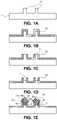
- FIGS. 1A-Eillustrate a method for making a heteroepitaxial layer, according to an embodiment of the present disclosure.
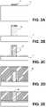
- FIGS. 2A-2Fillustrate a method for making heteroepitaxial layers, according to another embodiment of the present disclosure.
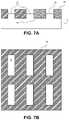
- FIG. 3illustrates a top view of a mask employed in an embodiment of the present disclosure.
- FIG. 4illustrates a device structure comprising heteroepitaxially grown layers, according to an embodiment of the present disclosure.
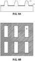
- FIGS. 5A-5Billustrate a schematic view of growth mask directly on a 2D substrate surface, according to an embodiment of the present disclosure.
- FIGS. 6A-6Billustrate a schematic view of growth mask flush with silicon pedestals, according to an embodiment of the present disclosure.
- FIGS. 7A-7Billustrate a schematic view of a growth mask extending beyond silicon pedestals, according to an embodiment of the present disclosure.
- FIGS. 8A-8Billustrate a schematic view of silicon pedestals extending beyond growth mask, according to an embodiment of the present disclosure.
- FIGS. 9A-9Billustrate a schematic view of non-faceted silicon pedestals extending beyond growth mask, according to an embodiment of the present disclosure.
- FIG. 10illustrates an isometric projection of a heterostructure FinFET showing an isolation layer, the source, gate and drain contacts labeled S, G and D respectively, according to an embodiment of the present disclosure.
- FIG. 11illustrates an isometric projection of a heterostructure FinFET with a dielectric isolation (shown as semi-transparent for clarity), according to an embodiment of the present disclosure.
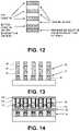
- FIG. 12illustrates a layered heterostructure for channel region of a device, according to an embodiment of the present disclosure.
- FIGS. 13-14illustrate schematic views of vertical nanowire transistors grown seed areas, according to an embodiment of the present disclosure.
- the present applicationis directed to devices and methods for forming devices in which a seed area for heteroepitaxial growth is formed on a semiconductor substrate.
- the seed areacomprises a two-dimensional area with at least one dimension less than about 100 nm.
- the seed areacomprises a linear surface dimension that ranges from about 10 nm to about 100 nm.
- seed areas having heteroepitaxial structures with linear surface dimensions less than 20 or 25 nmcan be employed.
- a heteroepitaxial layer comprising a second material that is different from the first materialcan be grown using the seed area to nucleate the epitaxial growth.
- the term “linear surface dimension”can refer to any linear dimension of the surface of the seed area, such as, for example, a width or diameter.
- Employing seed areas having relatively small dimensions in the manner disclosed hereincan have one or more of the following benefits: the ability to form heteroepitaxial structures with reduced numbers of defects compared with larger area heteroepitaxial layers; the ability to form heteroepitaxial structures with zero or substantially zero defects; the ability to form heteroepitaxial pillar structures that are flexible and/or that can accommodate strain better than heteroepitaxial layers grown on a planar substrate surface; or the ability to form small area heteroepitaxial films that can accommodate strain better than heteroepitaxial layers grown on a large area of a substrate surface.
- the nanoscale heteroepitaxial growth of the present disclosurecan exploit the greatly improved materials quality that occurs when the substrate, such as, for example a silicon fin, is nanoscale in lateral size.
- the substratesuch as, for example a silicon fin
- the heteroepitaxial techniques and devices of the present disclosurecan take advantage of the evolution of integrated circuits.
- the dimensions of a growth areaare reduced to below the average scale to nucleate a defect such as a threading dislocation, it is possible to grow heterogeneous materials without nucleating either threading dislocations or antisite defects (boundaries where two grains of the zinc-blende III-V crystal are misoriented by) 180°.
- the scale for this defect free growthis that at least one linear dimension of the growth area be much less than the mean distance between defects in a large area heteroepitaxial growth. In an embodiment, dimensions of about 100 nm or less can be employed, such as, for example, about 10 to about 20 nm.
- the table belowgives some typical dislocation densities and the corresponding average distance between dislocations. Note that to be suitable for silicon electronics, the incidence of threading dislocations that impact the electrical properties of an individual channel can be exceedingly low. Today's microprocessors contain as many as 3,000,000,000 transistors, and perhaps as many as 30,000,000,000 channels. With continued Moore's law scaling, this number will continue to climb exponentially. The allowed number of defected channels can be a very small fraction of the total number of channels.
- the prospects for defect-free nanoscale growthare further improved by the migration of silicon integrated circuits to FinFET architectures.
- the FinFET pedestalIn contrast to the growth in a simple opening atop a bulk substrate, the FinFET pedestal is significantly more compliant, e.g. it can share the strain (lattice displacement) associated with the lattice mismatch stress with the growing film.
- Control of strain in MOSFET channelsis an important aspect of modern integrated circuit manufacturing since the strain directly impacts the electronic properties of the material.
- Nanoscale growthprovides additional approaches to controlling this strain in the FinFET channel by adjusting the dimensions of the “fin” and the thickness and layer structure of the grown material.
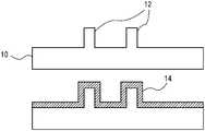
- FIG. 1A-Eillustrate a method for making a heteroepitaxial layer, according to an embodiment of the present disclosure.
- the methodcomprises providing a substrate 10 .
- suitable substratesinclude silicon wafers, silicon-on-insulator substrates, or other materials used as semiconductor substrates. Suitable substrates are commercially available and are well known in the art.
- the semiconductor substratecomprises silicon having a (001) facet exposed for processing.
- the cross-sections of substrate 10 shown in the figures hereincan have the ⁇ 110> direction oriented into the paper.
- Nanostructured pedestals 12are formed on the substrate.
- the Nanostructured pedestals 12are comprised of any suitable material capable of acting as a seed layer for subsequent epitaxial growth.
- suitable materialsinclude doped or undoped single crystal silicon.
- Other suitable materialsinclude single crystal III-V materials, such as GaAs and GaSb, which are common substrate materials in photonics and high-speed electronics; and single crystal GaN, sapphire and SiC. Any other single crystal material that provides a suitable nucleation surface for the desired epitaxial growth can be employed.
- the pedestals 12can be formed from the same material as the substrate, where the substrate is a single crystal material. In other embodiments, the pedestals can be a different material form the substrate. Any desired technique for forming the single crystal pedestals can be used.
- Such techniquesinclude various methods for patterning and etching the substrate surface. Suitable techniques are well known in the art. For purposes of strain relief as discussed below, it is useful to have the pedestals roughly as high or higher as the smallest in-plane dimension of the seed area.
- a selective growth mask layer 14is provided on a top surface and side surface of the pedestal.
- the selective growth mask layer 14can be provided over the entire perimeter of the sidewall surface.
- selective growth mask layer 14is formed on at least three sides of the pedestal, including the top surface and front and back sidewalls of a pedestal. Any suitable technique for forming the selective growth mask layer, such as oxidation of the semiconductor substrate surface, or deposition of material onto the surface, can be employed. Suitable methods for forming selective growth masks are well known in the art.
- a portion of the selective growth mask layer 14is removed to expose at least the top surface 16 of the pedestal 12 .
- Various suitable methodscan be employed to selectively remove the top portion of selective growth mask layer 14 . Examples include anisotropically etching to selectively remove the selective growth mask layer from the top surface of the pedestal; or formation of a non-conformal layer, such as by depositing and reflowing a layer followed by an etch back process. The etch back process can employ polishing, such as chemical mechanical polishing. Yet other examples of techniques for removing a portion of selective growth mask layer 14 will be discussed in greater detail below with respect to the method of FIG. 2 .
- the semiconductor material of pedestal 12can optionally be selectively etched back, as shown in FIG. 1D .
- the selective etch backremaining portions of the selective growth mask layer 14 form sidewall barriers 18 .
- the sidewall barriers 18can act to block defects, such as stacking faults that propagate, for example, along (111) directions (e.g., at an angle to the top surface).
- the remaining portion of pedestal 12comprises a (001) facet of silicon material exposed at the pedestal top surface.
- an epitaxial layeris grown on the remaining portion of pedestal 12 .
- the exposed top surface of pedestal 12provides a seed area for the epitaxial growth.
- the seed areacan have at least one dimension that is less than about 100 nm.
- Example configurations for the seed areainclude a rectangular area having with a width dimension ranging from about 10 nm to about 100 nm and a length dimension ranging from about 200 nm to about 2000 nm; or a circular area having a diameter ranging from, for example, about 10 nm to about 100 nm.
- the heteroepitaxial layercomprises a Group III-V semiconductor material.
- Group III-V semiconductor materialsinclude nitrogen-based materials, such as gallium nitride or other Group III-N semiconductors, such as AlGaN, indium nitride (InN), and indium gallium nitride (In x Ga 1 ⁇ x N).
- Group III-V semiconductor materialsinclude InAs and InAsSb, which have significantly higher electron mobilities and saturation velocities in comparison with Si. The techniques described also apply to semiconductor materials other than III-V materials, such as Ge.
- the growth of the epitaxial layeris directed by the seed area of the nanostructured pedestal surface.
- Epitaxial growthcopies the underlying crystal structure of the substrate, e.g., atoms line up as if they are a continuation of the starting crystal structure.
- the grown filmmight have the same symmetry as the seed area, but a different natural distance between atoms (this is the lattice mismatch mentioned above).
- FIG. 1Eillustrates an example of a heteroepitaxial nanostructure.
- the nanostructurecomprises the remaining pedestal 12 having a nano-dimensional top surface and a side surface; and the heteroepitaxial layer 20 (sometimes referred to herein as epitaxial layer 20 ) grown on the nano-dimensional top surface of the pedestal.
- the remaining selective growth mask layer 14extends above the surface of the pedestal 12 to form sidewall barriers 18 .
- the heteoepitaxial layer 20can grow between and above the sidewall barriers 18 , at which point the width dimensions of the heteroepitaxial layer nanostructure may increase to overlap the insulator, as shown, for example, in FIG. 1E .
- FIG. 1Eillustrates an example of a heteroepitaxial nanostructure.
- a portion of the heteroepitaxial layer 20 above the selective growth mask layerhas a polygonal cross-sectional shape having a first lateral vertex 20 a and a second lateral vertex 20 b opposing the first lateral vertex, a first lower linear surface 20 c of the polygonal cross-sectional shape and a first upper linear surface 20 d of the polygonal cross-sectional shape meeting at the first lateral vertex 20 a , a second lower linear surface 20 e of the polygonal cross-sectional shape and a second upper linear surface 20 f of the polygonal cross-sectional shape meeting at the second lateral vertex 20 b , the first upper linear surface 20 d and the second upper linear surface 20 f both sloping toward an apex 20 g of the heteroepitaxial layer and the first lower linear surface 20 c and the second lower linear surface 20 e both sloping toward the nanostructured pedestal 12 .
- the distance between the first lateral vertex 20 a and the second lateral vertex 20 b of the heteroepitaxial layer 20 in the final heteroepitaxial nanostructurecan be nano-dimensional. Additional growth can result in further enlargement of the heteroepitaxial layer as desired. Additional growth can result in further enlargement of the heteroepitaxial layer as desired.
- FIGS. 2A-2Fillustrate a method for making heteroepitaxial layers, according to another embodiment of the present disclosure.
- the substrate 10is a silicon substrate.
- Pedestals 12are formed by employing an etch mask 22 .
- the etch maskcan have width or diameter dimensions of about 1 micron or less.
- FIG. 3illustrates a top view, showing the etch mask 22 used to pattern the substrate.
- any other suitable shaped patterncan be employed, such as masks for forming square or rectangle features.
- the etch mask 22can be any suitable mask type, such as a patterned photoresist layer or hard mask formed of, for example, silicon oxide.
- the silicon substratecan be patterned by etching to form the pedestal 12 , as illustrated in FIG. 2B .
- Any suitable etching processcan be employed that will form the desired pedestal shape. In an embodiment, a dry etching process is employed.
- the etch mask 22can be removed.
- thermal oxidationcan then be carried out to form a selective growth mask layer 14 of silicon dioxide to a desired thickness.
- the thermal oxidation processconsumes the substrate material, so that the thicker the silicon dioxide layer, the smaller the resulting width dimension of the final pedestal 12 .
- the thickness of the silicon dioxidecan be varied so that the diameter or width of the silicon pedestal 12 is reduced to any desired size dimension.
- Example width dimensionscan be the same as those discussed above for FIG. 1 .
- the pedestal 12can be patterned to the desired final dimension during the etching step; followed by forming a selective growth mask layer to delineate the seed area by a process that does not consume the silicon to reduce the dimensions of the pedestal 12 .
- a non-conformal layer 24is formed over the pedestal 12 and selective growth mask layer 14 .
- Any suitable type of non-conformal layercan be employed.
- suitable non-conformal layersinclude doped silicon oxides, spin-on-glass, photoresist or other materials that can be deposited in liquid form, reflowed, polished or otherwise planarized to reduce surface topography. Suitable non-conformal layers are well known in the art.
- the non-conformal layercan be etched back until the selective growth mask layer 14 at the top of the pedestal 12 is exposed, as illustrated in FIG. 2E .
- the exposed portion of selective growth mask layer 14can be removed by the same or a different etch process as is used to etch back the non-conformal layer 24 .
- the remaining portion of the non-conformal layer 24can then be removed if desired, such as where the non-conformal layer is a polymer.
- the pedestal top surfacecan be used without further processing as a seed area for heteroepitaxial growth, if desired.
- a single crystal semiconductorgrows on the seed area 26 that is shown exposed in FIG. 2E .
- a further selective etch back of the seed material of pedestal 12can be carried out to form the sidewall barriers 18 prior to epitaxial growth, as illustrated in FIG. 2F .
- the etch back of the seed materialcan be performed by any suitable selective etch process, such as a dry etching process.
- Heteroepitaxial growthis then carried out between the sidewall barriers 18 .
- Sidewall barriers 18can block the propagation of defects, such as stacking faults and misfit dislocations, from the upper region of the heteroepitaxial layer.
- the resulting structureis shown in FIG. 4 , according to an embodiment of the present disclosure.
- the epitaxy conditionssuch as temperature and the ratio of precursor gases, can be controlled to allow for formation of a planar epitaxial layer surface.
- a planar GaN(001) facet at the top of GaN epi-layercan be grown using appropriate growth conditions.
- One of ordinary skill in the artwould be able to determine the desired conditions without undue experimentation.
- the pedestal structures of the present disclosurecan provide one or more of the following benefits: formation of heteroepitaxial materials with reduced defects; the selective growth mask layer 14 can prevent or reduce nucleation at the pedestal sidewalls, thereby isolating the nucleation during epitaxy to the top facet of the pedestal; pedestals can provide increased flexibility and/or the silicon pedestal structure can help relieve strain resulting from the lattice mismatch between the pedestal and the epitaxial material grown thereon.
- FIGS. 5A and 5Billustrate a semiconductor substrate 10 comprising a surface masked with any suitable selective growth mask 50 for patterning the seed areas 26 .
- the mask 50can be relatively thin compared to the thickness of the subsequently formed and fully-grown heteroepitaxial layer that is formed on seed areas 26 .
- a similar embodimentis contemplated that employs a thick growth mask 50 to prevent lateral overgrowth. Again, the term thick is relative to the thickness of the fully-grown heteroepitaxial layer subsequently grown on seed areas 26 .
- suitable growth masksinclude SiO 2 , Si 3 N 4 or combinations thereof.
- the dimensions of the seed areacan be any of the seed area dimensions described herein. In an embodiment, seed area dimensions in the substrate plane are ⁇ 10 nm wide by ⁇ 40 nm long. Similar dimensions can be employed for any of the seed areas illustrated in the embodiments of FIGS. 6-9 .
- FIGS. 6A and 6Billustrate an embodiment comprising semiconductor pedestals, or plateaus, protruding from the substrate 10 to form the seed areas 26 .
- Mask 50can be any appropriate growth mask such as SiO 2 , Si 3 N 4 or combinations thereof, that is arranged to be more or less flush with the top surface of the seed areas 26 .
- FIGS. 7A and 7Bcomprise semiconductor pedestals, or plateaus, protruding from the substrate 10 to form the seed areas 26 of the present disclosure, according to an embodiment of the present disclosure.
- Mask 50is formed to be higher than the top of seed areas 26 .
- FIGS. 8A and 8Billustrate an alternative embodiment in which the growth mask 50 is lower than the top of seed areas 26 , thereby allowing heteroepitaxial growth on the top and sides of the pedestals.
- FIGS. 9A and 9Billustrate an approach in which non-faceted pedestals protrude from the substrate, according to an embodiment of the present disclosure.
- the mask 50can be thinner than the top surface of seed areas 26 , thereby allowing growth on the top and sides of the pedestals, similar to the embodiment illustrated in FIG. 8A .
- the seed areascan comprise any of the semiconductor materials described for seed areas in the present disclosure; and the materials subsequently grown thereon can comprise any of the heteroepitaxial grown semiconductors described herein.
- the mask 50can be any of the mask materials described herein.
- FIG. 10illustrates an isometric projection of a FET device 70 that can be formed using heteroepitaxial layer structures, according to an embodiment of the present disclosure.
- Pedestal 12can be formed using any suitable process, such as with a masking layer to prevent growth on the sidewalls of the pedestal. In an embodiment, a growth mask such as that shown in FIG. 7A can be used.
- the silicon pedestal 12is shown with sloping sidewalls, but could have any other desired shape.
- heteroepitaxial growthproceeds from the exposed semiconductor surface, or seed area, of pedestal 12 .
- the seed area surfacecan comprise any suitable material, including any seed area materials discussed herein.
- the seed area surfaceis a Si(001) surface.
- An isolation layer 72can be grown on the seed area. Isolation layer 72 can be, for example, a large bandgap material, to prevent leakage of carriers from the channel into the silicon. As noted above, isolation layer 72 can also be a layer, such as an Al 0.98 Ga 0.02 As layer, that is easily oxidized following the growth to provide additional isolation.
- An alternative strategyis to dope the silicon so that it forms a p-n junction with the channel material, also reducing leakage of carriers into the silicon. Depending on the details of the bandgap alignment between the channel material and the silicon, isolation layer 72 may or may not be necessary.
- a layersuch as but not restricted to, a high Al concentration AlGaAs layer, which can be selectively oxidized during the device processing subsequent to growth of the heteroepitaxial layer.
- Thisallows epitaxial growth while at the same time providing the advantages of a semiconductor-on-oxide structure where the carriers are strongly confined to the channel.
- the aluminum oxide layercan be selectively removed to provide access for a gate-all-around configuration. Examples of this technique are described in U.S. Provisional Patent Application 61/752,741, entitled Gate-All-Around Metal-Oxide-Semiconductor Transistors with Gate Oxides, filed Jan. 15, 2013, the disclosure of which is hereby incorporated herein by reference in its entirety.
- Channel layer 74is grown.
- Channel layer 74is a heteroepitaxial layer and can comprise any suitable materials discussed herein for heteroepitaxial growth.
- the bandgap engineering that is common in III-V devicescan be used in devices of the present disclosure to, for example, grow higher bandgap cladding layers below and above the active channel layer. This can shield the carriers in the channel from surface defects and reduces scattering and improves carrier mobilities, saturation velocities, and lifetimes.
- channel layer 74can comprise several layers.
- channel layer 74can comprise a GaAs/InGaAs/GaAs structure in which the high mobility InGaAs material is clad with upper and lower high bandgap materials to shield the carriers from the higher point defect densities at the interface with the pedestal 12 or isolation layer and at the top surface of the growth.
- FIG. 12shows a possible layered heterostructure sequence for the channel layer 74 , according to an embodiment of the present disclosure.
- This structuretakes advantage of bandgap engineering that is well known for III-V devices.
- the structurecomprises a bottom large bandgap material in contact with a pedestal 12 .
- a bottom claddingfunctions to keep carriers away from the interface with pedestal 12 .
- a channel region and a top claddingare formed over the bottom cladding.
- the channel region and top claddingcan optionally be repeated a number of times, as shown, to provide increased current carrying capacity if thin channel regions, such as quantum wells, are desired.
- doping of the source and drain regionscan be carried out. This can include a masked ion implantation followed by an annealing step to activate the impurities. This will modify the growth layers by impurity induced diffusion to lower the resistance of the source-gate-drain transitions.
- a gate dielectric 76 and source “S”, drain “D” and gate “G” electrodes, as illustrated in FIG. 10can be formed by any suitable methods. Suitable methods are known in the art.
- FIG. 11shows an embodiment where a dielectric spacer 80 is used to planarize the structure following the S/G/D metallization.
- This layercan be thicker than the finFET and contact holes can be created for contacting the S/G/D, as is well known in the art.
- Another geometry of interestis a vertical channel.
- This embodimentlends itself to a gate all around configuration and has the significant advantage that the gate is self-aligned to the nanowires.
- the gate lengthcan be set by deposition processes which are much more controllable than lithography at nm dimensions. Examples of vertical MOSFETS are described in U.S. Pat. No. 8,344,361, the disclosure of which is hereby incorporated by reference in its entirety.
- the '361 patentdoes not explicitly discuss heterostructure growth from a silicon substrate, and is primarily about forming two and three terminal devices.
- FIGS. 13 and 14illustrate a process for forming high mobility channel vertical transistors based on nanowire growth from nanoscale Si seeds.
- the seed areacan have a linear surface dimension of 100 nm or less, such as 20 or 25 nm or less, or about 10 nm.
- the conceptproceeds in a source down configuration.
- the alternative drain down configurationis also available, as would be understood by one of ordinary skill in the art.
- the heteroepitaxial growthstarts from Si(001) pedestals 12 that can have any desired shape, such as square or round cross-sections, or extended into walls (e.g., a length dimension that is many times larger than the width dimension, such as 5, 10 or 100 times or more).
- An optional isolation layer 72is first grown to isolate the source from the Si material. Since the source region 82 is adjacent to the silicon in a source down embodiment, and a good contact can be provided, leakage into the silicon is not as important to the device performance as it was for the horizontal devices where the gate region was in direct contact with the silicon substrate material. Doping can be varied during the epitaxial growth to provide heavy doping in the source and drain regions 82 , 84 and reduced doping in the gate region 86 .
- the de-lineation of the source/gate/drain regions of the nanowiresrefers to doping levels during the growth.
- the vertical devicesare shown in parallel, e.g. all source, gate and drain contacts are connected to the same metallization. In an actual circuit, only some of the devices will be connected in parallel to provide current carrying capability; other devices would form the channels of different transistors in accordance with the circuit design.
- a dielectric layer 90is provided to isolate the silicon followed by formation of the source contact layer 92 .
- Appropriate annealing processescan be employed to assure good contact to the source regions of the nanowires. While all of the sources are shown connected in parallel; in practice, one or more of the nanowires will be in parallel to provide current carrying capability and others will be incorporated into different transistors as dictated by the circuit design.
- a field dielectric layer 94can be deposited to isolate the gate contact 96 from the source contact 92 . Initially, the field dielectric layer 94 can stop just short of the gate region to allow for oxidation of the nanowire to provide the gate dielectric 98 . The field dielectric 94 can then be continued to the middle of the gate region and gate contact 96 is provided.
- gate contact 96Following formation of gate contact 96 , additional field dielectric 100 can be deposited on top of the gate contact to completely cover the nanowires 88 . Then an etch back step can be carried out to expose the top of the drain regions and a drain contact 102 is provided. Additional processing can be used to define the various transistors and interconnections, as is the case in traditional integrated circuit manufacturing. There can be many variants on this basic process. For example, the gate oxide layer can be removed from the sidewall of the drain region and contact made using this sidewall in place of the top contact shown.
Landscapes
- Engineering & Computer Science (AREA)
- Physics & Mathematics (AREA)
- Chemical & Material Sciences (AREA)
- Condensed Matter Physics & Semiconductors (AREA)
- General Physics & Mathematics (AREA)
- Manufacturing & Machinery (AREA)
- Computer Hardware Design (AREA)
- Microelectronics & Electronic Packaging (AREA)
- Power Engineering (AREA)
- Nanotechnology (AREA)
- Crystallography & Structural Chemistry (AREA)
- Materials Engineering (AREA)
- Mathematical Physics (AREA)
- Theoretical Computer Science (AREA)
- Recrystallisation Techniques (AREA)
Abstract
Description
| Typical Threading | Average Distance | |||
| Dislocation | between | |||
| Material/Substrate | Density (cm−2) | Dislocations (μm) | ||
| Ge0.23Si0.77/Si(001) | 5 × 10⁵ | 14 | ||
| GaAs/Si(001) | 1 × 10⁵ | 3.2 | ||
| GaAs/GaAs | 1 × 10⁴ | 100 | ||
| InAs/Si(001) | 1 × 10⁷ | 3.2 | ||
| GaN/sapphire | 1 × 10⁹ | 0.32 | ||
| GaN/SiC | 5 × 10⁸ | 0.45 | ||
| GaN/GaN | 1 × 10⁶ | 10 | ||
| GaN/Si(111) | 1 × 10¹⁰ | 0.1 | ||
Claims (24)
Priority Applications (1)
| Application Number | Priority Date | Filing Date | Title |
|---|---|---|---|
| US16/748,327US11374106B2 (en) | 2012-07-17 | 2020-01-21 | Method of making heteroepitaxial structures and device formed by the method |
Applications Claiming Priority (5)
| Application Number | Priority Date | Filing Date | Title |
|---|---|---|---|
| US201261672713P | 2012-07-17 | 2012-07-17 | |
| US13/944,808US9142400B1 (en) | 2012-07-17 | 2013-07-17 | Method of making a heteroepitaxial layer on a seed area |
| US14/830,241US10141418B1 (en) | 2012-07-17 | 2015-08-19 | Device with heteroepitaxial structure made using a growth mask |
| US16/162,787US11342438B1 (en) | 2012-07-17 | 2018-10-17 | Device with heteroepitaxial structure made using a growth mask |
| US16/748,327US11374106B2 (en) | 2012-07-17 | 2020-01-21 | Method of making heteroepitaxial structures and device formed by the method |
Related Parent Applications (1)
| Application Number | Title | Priority Date | Filing Date |
|---|---|---|---|
| US16/162,787ContinuationUS11342438B1 (en) | 2012-07-17 | 2018-10-17 | Device with heteroepitaxial structure made using a growth mask |
Publications (2)
| Publication Number | Publication Date |
|---|---|
| US20200161448A1 US20200161448A1 (en) | 2020-05-21 |
| US11374106B2true US11374106B2 (en) | 2022-06-28 |
Family
ID=54107134
Family Applications (11)
| Application Number | Title | Priority Date | Filing Date |
|---|---|---|---|
| US13/944,808ActiveUS9142400B1 (en) | 2012-07-17 | 2013-07-17 | Method of making a heteroepitaxial layer on a seed area |
| US14/830,241Active2033-08-25US10141418B1 (en) | 2012-07-17 | 2015-08-19 | Device with heteroepitaxial structure made using a growth mask |
| US16/162,787ActiveUS11342438B1 (en) | 2012-07-17 | 2018-10-17 | Device with heteroepitaxial structure made using a growth mask |
| US16/746,853AbandonedUS20200212198A1 (en) | 2012-07-17 | 2020-01-18 | Method of making heteroepitaxial structures and device formed by the method |
| US16/748,327ActiveUS11374106B2 (en) | 2012-07-17 | 2020-01-21 | Method of making heteroepitaxial structures and device formed by the method |
| US16/748,095ActiveUS11342442B2 (en) | 2012-07-17 | 2020-01-21 | Semiconductor product comprising a heteroepitaxial layer grown on a seed area of a nanostructured pedestal |
| US16/747,930ActiveUS11456370B2 (en) | 2012-07-17 | 2020-01-21 | Semiconductor product comprising a heteroepitaxial layer grown on a seed area of a nanostructured pedestal |
| US16/747,765ActiveUS11342441B2 (en) | 2012-07-17 | 2020-01-21 | Method of forming a seed area and growing a heteroepitaxial layer on the seed area |
| US16/748,361ActiveUS11349011B2 (en) | 2012-07-17 | 2020-01-21 | Method of making heteroepitaxial structures and device formed by the method |
| US17/752,228PendingUS20220285526A1 (en) | 2012-07-17 | 2022-05-24 | Method of making heteroepitaxial structures and device formed by the method |
| US17/828,849AbandonedUS20220293768A1 (en) | 2012-07-17 | 2022-05-31 | Method of making heteroepitaxial structures and device formed by the method |
Family Applications Before (4)
| Application Number | Title | Priority Date | Filing Date |
|---|---|---|---|
| US13/944,808ActiveUS9142400B1 (en) | 2012-07-17 | 2013-07-17 | Method of making a heteroepitaxial layer on a seed area |
| US14/830,241Active2033-08-25US10141418B1 (en) | 2012-07-17 | 2015-08-19 | Device with heteroepitaxial structure made using a growth mask |
| US16/162,787ActiveUS11342438B1 (en) | 2012-07-17 | 2018-10-17 | Device with heteroepitaxial structure made using a growth mask |
| US16/746,853AbandonedUS20200212198A1 (en) | 2012-07-17 | 2020-01-18 | Method of making heteroepitaxial structures and device formed by the method |
Family Applications After (6)
| Application Number | Title | Priority Date | Filing Date |
|---|---|---|---|
| US16/748,095ActiveUS11342442B2 (en) | 2012-07-17 | 2020-01-21 | Semiconductor product comprising a heteroepitaxial layer grown on a seed area of a nanostructured pedestal |
| US16/747,930ActiveUS11456370B2 (en) | 2012-07-17 | 2020-01-21 | Semiconductor product comprising a heteroepitaxial layer grown on a seed area of a nanostructured pedestal |
| US16/747,765ActiveUS11342441B2 (en) | 2012-07-17 | 2020-01-21 | Method of forming a seed area and growing a heteroepitaxial layer on the seed area |
| US16/748,361ActiveUS11349011B2 (en) | 2012-07-17 | 2020-01-21 | Method of making heteroepitaxial structures and device formed by the method |
| US17/752,228PendingUS20220285526A1 (en) | 2012-07-17 | 2022-05-24 | Method of making heteroepitaxial structures and device formed by the method |
| US17/828,849AbandonedUS20220293768A1 (en) | 2012-07-17 | 2022-05-31 | Method of making heteroepitaxial structures and device formed by the method |
Country Status (1)
| Country | Link |
|---|---|
| US (11) | US9142400B1 (en) |
Cited By (1)
| Publication number | Priority date | Publication date | Assignee | Title |
|---|---|---|---|---|
| US20220328688A1 (en)* | 2021-04-08 | 2022-10-13 | Nexgen Power Systems, Inc. | Method and system for control of sidewall orientation in vertical gallium nitride field effect transistors |
Families Citing this family (10)
| Publication number | Priority date | Publication date | Assignee | Title |
|---|---|---|---|---|
| US9142400B1 (en) | 2012-07-17 | 2015-09-22 | Stc.Unm | Method of making a heteroepitaxial layer on a seed area |
| CN105531797A (en)* | 2013-06-28 | 2016-04-27 | 英特尔公司 | Nanostructures and nanofeatures with Si(111) planes on Si(100) wafers for III-N epitaxy |
| US10468406B2 (en) | 2014-10-08 | 2019-11-05 | Northrop Grumman Systems Corporation | Integrated enhancement mode and depletion mode device structure and method of making the same |
| US9865504B2 (en)* | 2016-03-04 | 2018-01-09 | Taiwan Semiconductor Manufacturing Company, Ltd. | Semiconductor device and manufacturing method thereof |
| US9691758B1 (en)* | 2016-03-11 | 2017-06-27 | Taiwan Semiconductor Manufacturing Co., Ltd. | Fin-type resistor |
| US10936756B2 (en) | 2017-01-20 | 2021-03-02 | Northrop Grumman Systems Corporation | Methodology for forming a resistive element in a superconducting structure |
| KR20230006054A (en) | 2017-11-30 | 2023-01-10 | 인텔 코포레이션 | Fin patterning for advanced integrated circuit structure fabrication |
| US10665666B2 (en)* | 2017-12-08 | 2020-05-26 | International Business Machines Corporation | Method of forming III-V on insulator structure on semiconductor substrate |
| KR20210026825A (en)* | 2019-09-02 | 2021-03-10 | 삼성전자주식회사 | Semiconductor devices including source/drain regions having antimony doped layer |
| WO2024084630A1 (en)* | 2022-10-19 | 2024-04-25 | 京セラ株式会社 | Semiconductor substrate, and method and apparatus for producing semiconductor substrate |
Citations (291)
| Publication number | Priority date | Publication date | Assignee | Title |
|---|---|---|---|---|
| US688555A (en) | 1901-07-19 | 1901-12-10 | Ernest A Eastmann | Buckle. |
| US3958040A (en) | 1973-09-07 | 1976-05-18 | U.S. Philips Corporation | Semiconductor device manufacture |
| US4222792A (en) | 1979-09-10 | 1980-09-16 | International Business Machines Corporation | Planar deep oxide isolation process utilizing resin glass and E-beam exposure |
| US4551394A (en) | 1984-11-26 | 1985-11-05 | Honeywell Inc. | Integrated three-dimensional localized epitaxial growth of Si with localized overgrowth of GaAs |
| US4571819A (en) | 1984-11-01 | 1986-02-25 | Ncr Corporation | Method for forming trench isolation structures |
| US4651179A (en) | 1983-01-21 | 1987-03-17 | Rca Corporation | Low resistance gallium arsenide field effect transistor |
| WO1989001235A1 (en) | 1987-08-03 | 1989-02-09 | Ford Microelectronics, Inc. | High effective barrier height transistor and method of making same |
| WO1989001236A1 (en) | 1987-07-24 | 1989-02-09 | Plessey Overseas Limited | A method of providing refilled trenches |
| US4876210A (en) | 1987-04-30 | 1989-10-24 | The University Of Delaware | Solution growth of lattice mismatched and solubility mismatched heterostructures |
| US5098850A (en) | 1989-06-16 | 1992-03-24 | Canon Kabushiki Kaisha | Process for producing substrate for selective crystal growth, selective crystal growth process and process for producing solar battery by use of them |
| US5166767A (en) | 1987-04-14 | 1992-11-24 | National Semiconductor Corporation | Sidewall contact bipolar transistor with controlled lateral spread of selectively grown epitaxial layer |
| US5229316A (en) | 1992-04-16 | 1993-07-20 | Micron Technology, Inc. | Semiconductor processing method for forming substrate isolation trenches |
| US5236546A (en) | 1987-01-26 | 1993-08-17 | Canon Kabushiki Kaisha | Process for producing crystal article |
| US5269852A (en) | 1991-05-27 | 1993-12-14 | Canon Kabushiki Kaisha | Crystalline solar cell and method for producing the same |
| US5403751A (en) | 1990-11-29 | 1995-04-04 | Canon Kabushiki Kaisha | Process for producing a thin silicon solar cell |
| US5417180A (en) | 1991-10-24 | 1995-05-23 | Rohm Co., Ltd. | Method for forming SOI structure |
| US5432120A (en) | 1992-12-04 | 1995-07-11 | Siemens Aktiengesellschaft | Method for producing a laterally limited single-crystal region with selective epitaxy and the employment thereof for manufacturing a bipolar transistor as well as a MOS transistor |
| US5451538A (en) | 1992-03-02 | 1995-09-19 | Motorola, Inc. | Method for forming a vertically integrated dynamic memory cell |
| US5453395A (en) | 1994-03-21 | 1995-09-26 | United Microelectronics Corp. | Isolation technology using liquid phase deposition |
| US5510645A (en) | 1993-06-02 | 1996-04-23 | Motorola, Inc. | Semiconductor structure having an air region and method of forming the semiconductor structure |
| US5661313A (en) | 1993-09-09 | 1997-08-26 | The United States Of America As Represented By The Secretary Of The Navy | Electroluminescent device in silicon on sapphire |
| US5702977A (en) | 1997-03-03 | 1997-12-30 | Taiwan Semiconductor Manufacturing Company, Ltd. | Shallow trench isolation method employing self-aligned and planarized trench fill dielectric layer |
| US5854126A (en) | 1997-03-31 | 1998-12-29 | Siemens Aktiengesellschaft | Method for forming metallization in semiconductor devices with a self-planarizing material |
| US5880007A (en) | 1997-09-30 | 1999-03-09 | Siemens Aktiengesellschaft | Planarization of a non-conformal device layer in semiconductor fabrication |
| US6037237A (en) | 1997-07-25 | 2000-03-14 | Samsung Electronics Co., Ltd. | Trench isolation methods utilizing composite oxide films |
| US6039803A (en) | 1996-06-28 | 2000-03-21 | Massachusetts Institute Of Technology | Utilization of miscut substrates to improve relaxed graded silicon-germanium and germanium layers on silicon |
| US6048775A (en) | 1999-05-24 | 2000-04-11 | Vanguard International Semiconductor Corporation | Method to make shallow trench isolation structure by HDP-CVD and chemical mechanical polish processes |
| US6049650A (en) | 1998-04-17 | 2000-04-11 | Seagate Technology, Inc. | Structure for micro-machine optical tooling and method for making and using |
| US6057207A (en) | 1998-03-25 | 2000-05-02 | Taiwan Semiconductor Manufacturing Company | Shallow trench isolation process using chemical-mechanical polish with self-aligned nitride mask on HDP-oxide |
| US6136727A (en) | 1997-12-19 | 2000-10-24 | Fuji Eletric Co., Ltd. | Method for forming thermal oxide film of silicon carbide semiconductor device |
| WO2000077831A2 (en) | 1999-06-11 | 2000-12-21 | Quester Technology, Inc. | Methods for regulating surface sensitivity of insulating films in semiconductor devices |
| KR20010009416A (en) | 1999-07-09 | 2001-02-05 | 윤종용 | Trench-type isolation method using a thin nitride film |
| KR20010036380A (en) | 1999-10-08 | 2001-05-07 | 정선종 | A trench formation method with tick edge oxide |
| US6228691B1 (en) | 1999-06-30 | 2001-05-08 | Intel Corp. | Silicon-on-insulator devices and method for producing the same |
| US20010006249A1 (en) | 1997-09-16 | 2001-07-05 | Eugene A Fitzgerald | Co-planar si and ge composite substrate and method of producing same |
| US6270353B1 (en) | 1999-06-07 | 2001-08-07 | International Business Machines Corporation | Low cost shallow trench isolation using non-conformal dielectric material |
| US6277706B1 (en) | 1997-06-13 | 2001-08-21 | Nec Corporation | Method of manufacturing isolation trenches using silicon nitride liner |
| US6291296B1 (en) | 1999-10-12 | 2001-09-18 | Advanced Micro Devices, Inc. | Method for removing anti-reflective coating layer using plasma etch process before contact CMP |
| KR20010112738A (en) | 2000-06-12 | 2001-12-21 | 윤종용 | Trench isolation method of semiconductor integrated circuit |
| US6362071B1 (en) | 2000-04-05 | 2002-03-26 | Motorola, Inc. | Method for forming a semiconductor device with an opening in a dielectric layer |
| US6387764B1 (en) | 1999-04-02 | 2002-05-14 | Silicon Valley Group, Thermal Systems Llc | Trench isolation process to deposit a trench fill oxide prior to sidewall liner oxidation growth |
| US6413802B1 (en) | 2000-10-23 | 2002-07-02 | The Regents Of The University Of California | Finfet transistor structures having a double gate channel extending vertically from a substrate and methods of manufacture |
| US6482715B2 (en) | 2000-12-16 | 2002-11-19 | Samsung Electronics Co., Ltd. | Method of forming shallow trench isolation layer in semiconductor device |
| US6486042B2 (en) | 2000-02-24 | 2002-11-26 | North Carolina State University | Methods of forming compound semiconductor layers using spaced trench arrays and semiconductor substrates formed thereby |
| US20030015704A1 (en) | 2001-07-23 | 2003-01-23 | Motorola, Inc. | Structure and process for fabricating semiconductor structures and devices utilizing the formation of a compliant substrate for materials used to form the same including intermediate surface cleaning |
| US6511888B1 (en) | 1999-11-12 | 2003-01-28 | Samsung Electronics Co., Ltd. | Method of fabricating a semiconductor device using trench isolation method including hydrogen annealing step |
| US20030054608A1 (en) | 2001-09-17 | 2003-03-20 | Vanguard International Semiconductor Corporation | Method for forming shallow trench isolation in semiconductor device |
| US6541349B2 (en) | 2001-01-18 | 2003-04-01 | International Business Machines Corporation | Shallow trench isolation using non-conformal dielectric and planarizatrion |
| US6555845B2 (en) | 1997-03-13 | 2003-04-29 | Nec Corporation | Method for manufacturing group III-V compound semiconductors |
| US20030089899A1 (en) | 2000-08-22 | 2003-05-15 | Lieber Charles M. | Nanoscale wires and related devices |
| US20030168002A1 (en) | 2001-11-16 | 2003-09-11 | Zaidi Saleem H. | Nanostructures for hetero-expitaxial growth on silicon substrates |
| US6642090B1 (en) | 2002-06-03 | 2003-11-04 | International Business Machines Corporation | Fin FET devices from bulk semiconductor and method for forming |
| US6753555B2 (en) | 1999-11-15 | 2004-06-22 | Matsushita Electric Industrial Co., Ltd. | DTMOS device having low threshold voltage |
| KR20040055463A (en) | 2002-12-21 | 2004-06-26 | 주식회사 하이닉스반도체 | Method for forming isolation layer in semiconductor device |
| US6762483B1 (en) | 2003-01-23 | 2004-07-13 | Advanced Micro Devices, Inc. | Narrow fin FinFET |
| US6794718B2 (en) | 2002-12-19 | 2004-09-21 | International Business Machines Corporation | High mobility crystalline planes in double-gate CMOS technology |
| US6803602B2 (en) | 1999-10-14 | 2004-10-12 | Cree, Inc. | Single step pendeo- and lateral epitaxial overgrowth of Group III-nitride epitaxial layers with Group III-nitride buffer layer and resulting structures |
| US6806115B2 (en) | 2001-11-02 | 2004-10-19 | Sharp Kabushiki Kaisha | Semiconductor light emitting device and method for producing the same |
| US6809351B2 (en) | 2001-03-07 | 2004-10-26 | Nec Corporation | Group III-V compound semiconductor crystal structure and method of epitaxial growth of the same as well as semiconductor device including the same |
| US6812119B1 (en) | 2003-07-08 | 2004-11-02 | Advanced Micro Devices, Inc. | Narrow fins by oxidation in double-gate finfet |
| US6815241B2 (en) | 2002-09-25 | 2004-11-09 | Cao Group, Inc. | GaN structures having low dislocation density and methods of manufacture |
| US6828646B2 (en) | 2001-10-17 | 2004-12-07 | Stmicroelectronics Sa | Isolating trench and manufacturing process |
| US6835618B1 (en) | 2003-08-05 | 2004-12-28 | Advanced Micro Devices, Inc. | Epitaxially grown fin for FinFET |
| US6838322B2 (en) | 2003-05-01 | 2005-01-04 | Freescale Semiconductor, Inc. | Method for forming a double-gated semiconductor device |
| US20050017304A1 (en)* | 2003-06-13 | 2005-01-27 | Daisuke Matsushita | Field effect transistor and method of manufacturing the same |
| US6855990B2 (en) | 2002-11-26 | 2005-02-15 | Taiwan Semiconductor Manufacturing Co., Ltd | Strained-channel multiple-gate transistor |
| US6858478B2 (en) | 2002-08-23 | 2005-02-22 | Intel Corporation | Tri-gate devices and methods of fabrication |
| US6873009B2 (en) | 1999-05-13 | 2005-03-29 | Hitachi, Ltd. | Vertical semiconductor device with tunnel insulator in current path controlled by gate electrode |
| US20050077553A1 (en) | 2003-10-14 | 2005-04-14 | Kim Sung-Min | Methods of forming multi fin FETs using sacrificial fins and devices so formed |
| US6881651B2 (en) | 1999-05-21 | 2005-04-19 | Toyoda Gosei Co., Ltd. | Methods and devices using group III nitride compound semiconductor |
| US6885055B2 (en) | 2003-02-04 | 2005-04-26 | Lee Jong-Ho | Double-gate FinFET device and fabricating method thereof |
| WO2005048330A1 (en) | 2003-11-12 | 2005-05-26 | Advancesis Limited | Formation of lattice-tuning semiconductor substrates |
| US6919258B2 (en) | 2003-10-02 | 2005-07-19 | Freescale Semiconductor, Inc. | Semiconductor device incorporating a defect controlled strained channel structure and method of making the same |
| US6921673B2 (en) | 2001-03-27 | 2005-07-26 | Sony Corporation | Nitride semiconductor device and method of manufacturing the same |
| US20050167655A1 (en) | 2004-01-29 | 2005-08-04 | International Business Machines Corporation | Vertical nanotube semiconductor device structures and methods of forming the same |
| US20050184302A1 (en) | 2000-04-04 | 2005-08-25 | Toshimasa Kobayashi | Nitride semiconductor device and method of manufacturing the same |
| WO2005098963A1 (en) | 2004-03-31 | 2005-10-20 | Intel Corporation | A bulk non-planar transistor having a strained channel with enhanced mobility and methods of fabrication |
| US6958254B2 (en) | 2001-05-08 | 2005-10-25 | Btg International Limited | Method to produce germanium layers |
| US6977194B2 (en) | 2003-10-30 | 2005-12-20 | International Business Machines Corporation | Structure and method to improve channel mobility by gate electrode stress modification |
| US6982435B2 (en) | 1999-03-31 | 2006-01-03 | Toyoda Gosei Co., Ltd. | Group III nitride compound semiconductor device and method for producing the same |
| US6994751B2 (en) | 2001-02-27 | 2006-02-07 | Sanyo Electric Co., Ltd. | Nitride-based semiconductor element and method of forming nitride-based semiconductor |
| US7002207B2 (en) | 2002-10-01 | 2006-02-21 | Samsung Electronics Co., Ltd. | Field effect transistors having multiple stacked channels |
| US7012314B2 (en) | 2002-12-18 | 2006-03-14 | Agere Systems Inc. | Semiconductor devices with reduced active region defects and unique contacting schemes |
| US7038289B2 (en) | 2001-06-14 | 2006-05-02 | Stmicroelectronics Sa | Deep insulating trench |
| US7045401B2 (en) | 2003-06-23 | 2006-05-16 | Sharp Laboratories Of America, Inc. | Strained silicon finFET device |
| US20060113603A1 (en) | 2004-12-01 | 2006-06-01 | Amberwave Systems Corporation | Hybrid semiconductor-on-insulator structures and related methods |
| US7071048B2 (en) | 2003-10-31 | 2006-07-04 | Samsung Electronics Co., Ltd. | Methods of fabricating fin field effect transistors having capping insulation layers |
| US7074662B2 (en) | 2003-07-24 | 2006-07-11 | Samsung Electronics Co., Ltd. | Methods for fabricating fin field effect transistors using a protective layer to reduce etching damage |
| US20060154439A1 (en) | 2005-01-13 | 2006-07-13 | Samsung Electronics Co., Ltd. | Method of fabricating semiconductor device |
| US20060207647A1 (en) | 2005-03-16 | 2006-09-21 | General Electric Company | High efficiency inorganic nanorod-enhanced photovoltaic devices |
| US7118987B2 (en) | 2004-01-29 | 2006-10-10 | Taiwan Semiconductor Manufacturing Co., Ltd. | Method of achieving improved STI gap fill with reduced stress |
| US7128846B2 (en) | 2002-02-28 | 2006-10-31 | Toyoda Gosei Co., Ltd. | Process for producing group III nitride compound semiconductor |
| WO2006125040A2 (en) | 2005-05-17 | 2006-11-23 | Amberwave Systems Corporation | Lattice-mismatched semiconductor structures with reduced dislocation defect densities related methods for device fabrication |
| US7141506B2 (en) | 2001-06-22 | 2006-11-28 | Sharp Kabushiki Kaisha | Method for evaluating dependence of properties of semiconductor substrate on plane orientation and semiconductor device using the same |
| US7148541B2 (en) | 2003-02-19 | 2006-12-12 | Samsung Electronics Co., Ltd. | Vertical channel field effect transistors having insulating layers thereon |
| US7176115B2 (en) | 2003-03-20 | 2007-02-13 | Matsushita Electric Industrial Co., Ltd. | Method of manufacturing Group III nitride substrate and semiconductor device |
| US7176067B2 (en) | 2003-06-27 | 2007-02-13 | Samsung Electronics Co., Ltd. | Methods of fabricating fin field effect transistors |
| US7176549B2 (en) | 1995-10-24 | 2007-02-13 | Micron Technology, Inc. | Shallow trench isolation using low dielectric constant insulator |
| US7196374B1 (en) | 2003-09-03 | 2007-03-27 | Advanced Micro Devices, Inc. | Doped structure for FinFET devices |
| US7198995B2 (en) | 2003-12-12 | 2007-04-03 | International Business Machines Corporation | Strained finFETs and method of manufacture |
| US7205201B2 (en) | 2004-08-09 | 2007-04-17 | System General Corp. | CMOS compatible process with different-voltage devices |
| US7205210B2 (en) | 2004-02-17 | 2007-04-17 | Freescale Semiconductor, Inc. | Semiconductor structure having strained semiconductor and method therefor |
| US7220658B2 (en) | 2002-12-16 | 2007-05-22 | The Regents Of The University Of California | Growth of reduced dislocation density non-polar gallium nitride by hydride vapor phase epitaxy |
| US7226504B2 (en) | 2002-01-31 | 2007-06-05 | Sharp Laboratories Of America, Inc. | Method to form thick relaxed SiGe layer with trench structure |
| US7229901B2 (en) | 2004-12-16 | 2007-06-12 | Wisconsin Alumni Research Foundation | Fabrication of strained heterojunction structures |
| US7238586B2 (en) | 2005-07-21 | 2007-07-03 | United Microelectronics Corp. | Seamless trench fill method utilizing sub-atmospheric pressure chemical vapor deposition technique |
| US7247534B2 (en) | 2003-11-19 | 2007-07-24 | International Business Machines Corporation | Silicon device on Si:C-OI and SGOI and method of manufacture |
| US20070183185A1 (en)* | 2006-01-11 | 2007-08-09 | The Regents Of The University Of California | Finfet-based sram with feedback |
| US20070187668A1 (en) | 2006-02-16 | 2007-08-16 | Takashi Noguchi | Crystal substrates and methods of fabricating the same |
| US7268058B2 (en) | 2004-01-16 | 2007-09-11 | Intel Corporation | Tri-gate transistors and methods to fabricate same |
| US20070221956A1 (en) | 2006-03-23 | 2007-09-27 | Kabushiki Kaisha Toshiba | Semiconductor device and method of fabricating the same |
| US20070235819A1 (en) | 2006-03-14 | 2007-10-11 | Atsushi Yagishita | Semiconductor device and method for manufacturing the same |
| US7285820B2 (en) | 2004-09-01 | 2007-10-23 | Samsung Electronics Co., Ltd. | Flash memory device using semiconductor fin and method thereof |
| US20070267722A1 (en) | 2006-05-17 | 2007-11-22 | Amberwave Systems Corporation | Lattice-mismatched semiconductor structures with reduced dislocation defect densities and related methods for device fabrication |
| US7309626B2 (en) | 2005-11-15 | 2007-12-18 | International Business Machines Corporation | Quasi self-aligned source/drain FinFET process |
| US7317230B2 (en) | 2004-02-10 | 2008-01-08 | Samsung Electronics Co., Ltd. | Fin FET structure |
| US7323375B2 (en) | 2004-05-04 | 2008-01-29 | Samsung Electronics Co., Ltd. | Fin field effect transistor device and method of fabricating the same |
| US7326608B2 (en) | 2004-12-03 | 2008-02-05 | Samsung Electronic Co., Ltd. | Fin field effect transistor and method of manufacturing the same |
| US20080036038A1 (en) | 2006-03-10 | 2008-02-14 | Hersee Stephen D | PULSED GROWTH OF CATALYST-FREE GROWITH OF GaN NANOWIRES AND APPLICATION IN GROUP III NITRIDE SEMICONDUCTOR BULK MATERIAL |
| US20080070355A1 (en) | 2006-09-18 | 2008-03-20 | Amberwave Systems Corporation | Aspect ratio trapping for mixed signal applications |
| US20080073667A1 (en) | 2006-09-27 | 2008-03-27 | Amberwave Systems Corporation | Tri-gate field-effect transistors formed by aspect ratio trapping |
| US20080099785A1 (en) | 2006-09-07 | 2008-05-01 | Amberwave Systems Coporation | Defect Reduction Using Aspect Ratio Trapping |
| US7385247B2 (en) | 2004-01-17 | 2008-06-10 | Samsung Electronics Co., Ltd. | At least penta-sided-channel type of FinFET transistor |
| US7385237B2 (en) | 2004-03-11 | 2008-06-10 | Samsung Electronics Co., Ltd. | Fin field effect transistors with low resistance contact structures |
| US20080149944A1 (en) | 2006-12-22 | 2008-06-26 | Qunano Ab | Led with upstanding nanowire structure and method of producing such |
| US20080149914A1 (en)* | 2006-12-22 | 2008-06-26 | Qunano Ab | Nanoelectronic structure and method of producing such |
| US20080187018A1 (en) | 2006-10-19 | 2008-08-07 | Amberwave Systems Corporation | Distributed feedback lasers formed via aspect ratio trapping |
| US7411241B2 (en) | 2005-03-28 | 2008-08-12 | Samsung Electronics Co., Ltd. | Vertical type nanotube semiconductor device |
| US20080230802A1 (en) | 2003-12-23 | 2008-09-25 | Erik Petrus Antonius Maria Bakkers | Semiconductor Device Comprising a Heterojunction |
| US20080315430A1 (en) | 2007-06-22 | 2008-12-25 | Qimonda Ag | Nanowire vias |
| US7488385B2 (en) | 2002-05-28 | 2009-02-10 | Lumilog | Method for epitaxial growth of a gallium nitride film separated from its substrate |
| US20090039361A1 (en) | 2005-05-17 | 2009-02-12 | Amberwave Systems Corporation | Lattice-mismatched semiconductor structures with reduced dislocation defect densities and related methods for device fabrication |
| US7504323B2 (en) | 1997-10-30 | 2009-03-17 | Sumitomo Electric Industries, Ltd. | GaN single crystal substrate and method of making the same |
| US7507628B2 (en) | 2006-10-31 | 2009-03-24 | Hynix Semiconductor Inc. | Method of manufacturing a non-volatile memory device |
| US7514328B2 (en) | 2003-06-26 | 2009-04-07 | Mears Technologies, Inc. | Method for making a semiconductor device including shallow trench isolation (STI) regions with a superlattice therebetween |
| US7514739B2 (en) | 2004-08-27 | 2009-04-07 | Samsung Electronics Co., Ltd | Nonvolatile semiconductor device and method of fabricating the same |
| US7514366B2 (en) | 2004-08-24 | 2009-04-07 | Micron Technology, Inc. | Methods for forming shallow trench isolation |
| US7525160B2 (en) | 2005-12-27 | 2009-04-28 | Intel Corporation | Multigate device with recessed strain regions |
| US7535061B2 (en) | 2003-06-30 | 2009-05-19 | Samsung Electronics Co., Ltd. | Fin-field effect transistors (Fin-FETs) having protection layers |
| US7547610B2 (en) | 2006-09-29 | 2009-06-16 | Advanced Micro Devices, Inc. | Method of making a semiconductor device comprising isolation trenches inducing different types of strain |
| US7554165B2 (en) | 2007-04-26 | 2009-06-30 | Kabushiki Kaisha Toshiba | Semiconductor device |
| US7582516B2 (en) | 2006-06-06 | 2009-09-01 | International Business Machines Corporation | CMOS devices with hybrid channel orientations, and methods for fabricating the same using faceted epitaxy |
| US20090223558A1 (en) | 2008-03-07 | 2009-09-10 | Tsinghua University | Solar cell |
| KR20090097424A (en) | 2008-03-11 | 2009-09-16 | 주식회사 하이닉스반도체 | Device Separator Formation Method of Semiconductor Device |
| EP1555688B1 (en) | 2004-01-17 | 2009-11-11 | Samsung Electronics Co., Ltd. | Method of manufacturing a multi-sided-channel finfet transistor |
| US7626246B2 (en) | 2005-07-26 | 2009-12-01 | Amberwave Systems Corporation | Solutions for integrated circuit integration of alternative active area materials |
| US7667271B2 (en) | 2007-04-27 | 2010-02-23 | Taiwan Semiconductor Manufacturing Company, Ltd. | Fin field-effect transistors |
| US7671420B2 (en) | 2005-01-04 | 2010-03-02 | Samsung Electronics Co., Ltd. | Semiconductor devices having faceted channels and methods of fabricating such devices |
| US7777250B2 (en) | 2006-03-24 | 2010-08-17 | Taiwan Semiconductor Manufacturing Company, Ltd. | Lattice-mismatched semiconductor structures and related methods for device fabrication |
| US7785706B2 (en) | 2007-03-28 | 2010-08-31 | Siltronic Ag | Semiconductor wafer and process for its production |
| US7791108B2 (en) | 2006-01-25 | 2010-09-07 | Nxp B.V. | Nanowire tunneling transistor |
| US7807523B2 (en) | 2005-07-01 | 2010-10-05 | Synopsys, Inc. | Sequential selective epitaxial growth |
| US7842566B2 (en) | 2006-12-08 | 2010-11-30 | Samsung Electronics Co., Ltd. | FinFET and method of manufacturing the same |
| US7851790B2 (en) | 2008-12-30 | 2010-12-14 | Intel Corporation | Isolated Germanium nanowire on Silicon fin |
| US7863122B2 (en) | 2006-06-29 | 2011-01-04 | International Business Machines Corporation | Bulk FinFET device |
| US7875925B2 (en) | 2007-08-28 | 2011-01-25 | Kabushiki Kaisha Toshiba | Nonvolatile semiconductor memory device |
| US7875958B2 (en) | 2006-09-27 | 2011-01-25 | Taiwan Semiconductor Manufacturing Company, Ltd. | Quantum tunneling devices and circuits with lattice-mismatched semiconductor structures |
| US20110031470A1 (en) | 2009-06-26 | 2011-02-10 | Axel Scherer | Methods for fabricating passivated silicon nanowires and devices thus obtained |
| US7888201B2 (en) | 2003-11-04 | 2011-02-15 | Taiwan Semiconductor Manufacturing Company, Ltd. | Semiconductor-on-insulator SRAM configured using partially-depleted and fully-depleted transistors |
| US7893506B2 (en) | 2005-02-23 | 2011-02-22 | Intel Corporation | Field effect transistor with narrow bandgap source and drain regions and method of fabrication |
| US7892956B2 (en) | 2007-09-24 | 2011-02-22 | International Business Machines Corporation | Methods of manufacture of vertical nanowire FET devices |
| US20110042744A1 (en) | 2009-08-18 | 2011-02-24 | International Business Machines Corporation | Method of forming extremely thin semiconductor on insulator (etsoi) device without ion implantation |
| US7901968B2 (en) | 2006-03-23 | 2011-03-08 | Asm America, Inc. | Heteroepitaxial deposition over an oxidized surface |
| US7906814B2 (en) | 2006-09-01 | 2011-03-15 | Snu R&Db Foundation | Fin field effect transistor having low leakage current and method of manufacturing the FinFET |
| US7910492B2 (en) | 2003-04-04 | 2011-03-22 | Qunano Ab | Nanowhiskers with PN junctions, doped nanowhiskers, and methods for preparing them |
| US7915642B2 (en) | 2008-12-30 | 2011-03-29 | Intel Corporation | Apparatus and methods for forming a modulation doped non-planar transistor |
| US20110097881A1 (en) | 2009-10-23 | 2011-04-28 | Imec | Method of Forming Mono-Crystalline Germanium or Silicon Germanium |
| US20110100411A1 (en) | 2007-05-07 | 2011-05-05 | Wisconsin Alumni Research Foundation | Semiconductor nanowire thermoelectric materials and devices, and processes for producing same |
| US20110101456A1 (en) | 2009-10-30 | 2011-05-05 | Jan Hoentschel | Strain engineering in three-dimensional transistors based on globally strained semiconductor base layers |
| US7939862B2 (en) | 2007-05-30 | 2011-05-10 | Synopsys, Inc. | Stress-enhanced performance of a FinFet using surface/channel orientations and strained capping layers |
| US7939889B2 (en) | 2007-10-16 | 2011-05-10 | Taiwan Semiconductor Manufacturing Company, Ltd. | Reducing resistance in source and drain regions of FinFETs |
| US20110140085A1 (en) | 2009-11-19 | 2011-06-16 | Homyk Andrew P | Methods for fabricating self-aligning arrangements on semiconductors |
| US20110163242A1 (en) | 2008-07-24 | 2011-07-07 | The Regents Of The University Of California | Layered semiconductor neutron detectors |
| US20110169012A1 (en) | 2007-10-04 | 2011-07-14 | Hersee Stephen D | NANOWIRE AND LARGER GaN BASED HEMTS |
| US7994028B2 (en) | 2007-09-07 | 2011-08-09 | International Business Machines Corporation | Structures having lattice-mismatched single-crystalline semiconductor layers on the same lithographic level and methods of manufacturing the same |
| US7995892B2 (en) | 2007-06-01 | 2011-08-09 | Lawrence Livermore National Security, Llc | Low loss, high and low index contrast waveguides in semiconductors |
| US20110193141A1 (en) | 2010-02-11 | 2011-08-11 | Taiwan Semiconductor Manufacturing Company, Ltd. | Method of fabricating a finfet device |
| US20110193175A1 (en) | 2010-02-09 | 2011-08-11 | Taiwan Semiconductor Manufacturing Co., Ltd. | Lower parasitic capacitance finfet |
| US20110233512A1 (en) | 2005-08-16 | 2011-09-29 | The Regents Of The University Of California | Vertical integrated silicon nanowire field effect transistors and methods of fabrication |
| US8035153B2 (en) | 2007-04-26 | 2011-10-11 | Spansion Llc | Self-aligned patterning method by using non-conformal film and etch for flash memory and other semiconductor applications |
| WO2011135432A1 (en) | 2010-04-27 | 2011-11-03 | Von Kaenel Hans | Dislocation and stress management by mask-less processes using substrate patterning and methods for device fabrication |
| US20110272763A1 (en) | 2009-02-12 | 2011-11-10 | Yuichiro Sasaki | Semiconductor device and method for fabricating the same |
| US8062951B2 (en) | 2007-12-10 | 2011-11-22 | International Business Machines Corporation | Method to increase effective MOSFET width |
| US8062963B1 (en) | 2010-10-08 | 2011-11-22 | Taiwan Semiconductor Manufacturing Company, Ltd. | Method of fabricating a semiconductor device having an epitaxy region |
| US8063450B2 (en) | 2006-09-19 | 2011-11-22 | Qunano Ab | Assembly of nanoscaled field effect transistors |
| US8072012B2 (en) | 2006-09-15 | 2011-12-06 | Imec | Tunnel effect transistors based on elongate monocrystalline nanostructures having a heterostructure |
| US8101473B2 (en) | 2009-07-10 | 2012-01-24 | Hewlett-Packard Development Company, L.P. | Rounded three-dimensional germanium active channel for transistors and sensors |
| US8120060B2 (en) | 2005-11-01 | 2012-02-21 | Massachusetts Institute Of Technology | Monolithically integrated silicon and III-V electronics |
| US8129769B2 (en) | 2008-12-16 | 2012-03-06 | Elpida Memory, Inc. | Semiconductor device and manufacturing method thereof |
| US8129763B2 (en) | 2008-02-07 | 2012-03-06 | International Business Machines Corporation | Metal-oxide-semiconductor device including a multiple-layer energy filter |
| US8133797B2 (en) | 2008-05-16 | 2012-03-13 | Novellus Systems, Inc. | Protective layer to enable damage free gap fill |
| US8134142B2 (en) | 2006-01-25 | 2012-03-13 | Nxp B.V. | Tunneling transistor with barrier |
| US20120091465A1 (en) | 2010-10-13 | 2012-04-19 | Soraa, Inc. | Method of Making Bulk InGaN Substrates and Devices Thereon |
| US20120091538A1 (en) | 2010-10-13 | 2012-04-19 | Taiwan Semiconductor Manufacturing Company, Ltd. | Finfet and method of fabricating the same |
| US8169025B2 (en) | 2010-01-19 | 2012-05-01 | International Business Machines Corporation | Strained CMOS device, circuit and method of fabrication |
| US8183667B2 (en) | 2008-06-03 | 2012-05-22 | Taiwan Semiconductor Manufacturing Co., Ltd. | Epitaxial growth of crystalline material |
| US8212336B2 (en) | 2008-09-15 | 2012-07-03 | Acorn Technologies, Inc. | Field effect transistor source or drain with a multi-facet surface |
| US8236634B1 (en) | 2011-03-17 | 2012-08-07 | International Business Machines Corporation | Integration of fin-based devices and ETSOI devices |
| US20120217474A1 (en) | 2011-02-25 | 2012-08-30 | Agency For Science, Technology And Research | Photonic device and method of making the same |
| US8263462B2 (en) | 2008-12-31 | 2012-09-11 | Taiwan Semiconductor Manufacturing Company, Ltd. | Dielectric punch-through stoppers for forming FinFETs having dual fin heights |
| US8264032B2 (en) | 2009-09-01 | 2012-09-11 | Taiwan Semiconductor Manufacturing Company, Ltd. | Accumulation type FinFET, circuits and fabrication method thereof |
| US8264021B2 (en) | 2009-10-01 | 2012-09-11 | Taiwan Semiconductor Manufacturing Company, Ltd. | Finfets and methods for forming the same |
| US8274097B2 (en) | 2008-07-01 | 2012-09-25 | Taiwan Semiconductor Manufacturing Company, Ltd. | Reduction of edge effects from aspect ratio trapping |
| US8288756B2 (en) | 2007-11-30 | 2012-10-16 | Advanced Micro Devices, Inc. | Hetero-structured, inverted-T field effect transistor |
| US8304817B2 (en) | 2007-10-05 | 2012-11-06 | Kabushiki Kaisha Toshiba | Field effect transistor and method for manufacturing the same |
| US8313999B2 (en) | 2009-12-23 | 2012-11-20 | Intel Corporation | Multi-gate semiconductor device with self-aligned epitaxial source and drain |
| US8324660B2 (en) | 2005-05-17 | 2012-12-04 | Taiwan Semiconductor Manufacturing Company, Ltd. | Lattice-mismatched semiconductor structures with reduced dislocation defect densities and related methods for device fabrication |
| US8330143B2 (en) | 2005-06-16 | 2012-12-11 | Qunano Ab | Semiconductor nanowire transistor |
| US20120319211A1 (en) | 2011-06-16 | 2012-12-20 | Taiwan Semiconductor Manufacturing Company, Ltd. | Strained channel field effect transistor |
| US8344242B2 (en) | 2007-09-07 | 2013-01-01 | Taiwan Semiconductor Manufacturing Company, Ltd. | Multi-junction solar cells |
| US8362575B2 (en) | 2009-09-29 | 2013-01-29 | Taiwan Semiconductor Manufacturing Company, Ltd. | Controlling the shape of source/drain regions in FinFETs |
| US8362568B2 (en) | 2009-08-28 | 2013-01-29 | International Business Machines Corporation | Recessed contact for multi-gate FET optimizing series resistance |
| US8367498B2 (en) | 2010-10-18 | 2013-02-05 | Taiwan Semiconductor Manufacturing Company, Ltd. | Fin-like field effect transistor (FinFET) device and method of manufacturing same |
| US8367520B2 (en) | 2008-09-22 | 2013-02-05 | Soitec | Methods and structures for altering strain in III-nitride materials |
| US8383503B2 (en) | 2009-08-05 | 2013-02-26 | GlobalFoundries, Inc. | Methods for forming semiconductor structures using selectively-formed sidewall spacers |
| US8384195B2 (en) | 2010-05-04 | 2013-02-26 | Imec | Nanochannel device and method for manufacturing thereof |
| US8384196B2 (en) | 2008-09-19 | 2013-02-26 | Taiwan Semiconductor Manufacturing Company, Ltd. | Formation of devices by epitaxial layer overgrowth |
| US20130049068A1 (en) | 2011-08-30 | 2013-02-28 | Taiwan Semiconductor Manufacturing Company, Ltd. | Finfet device having a channel defined in a diamond-like shape semiconductor structure |
| US8399931B2 (en) | 2010-06-30 | 2013-03-19 | Taiwan Semiconductor Manufacturing Company, Ltd. | Layout for multiple-fin SRAM cell |
| US8415718B2 (en) | 2009-10-30 | 2013-04-09 | Taiwan Semiconductor Manufacturing Company, Ltd. | Method of forming epi film in substrate trench |
| US8415209B2 (en) | 2010-04-19 | 2013-04-09 | Imec | Method of manufacturing a complementary nanowire tunnel field effect transistor semiconductor device |
| US20130092984A1 (en) | 2011-10-13 | 2013-04-18 | Taiwan Semiconductor Manufacturing Company, Ltd. | Finfet device and method of manufacturing same |
| US8426923B2 (en) | 2009-12-02 | 2013-04-23 | Taiwan Semiconductor Manufacturing Company, Ltd. | Multiple-gate semiconductor device and method |
| US8435845B2 (en) | 2011-04-06 | 2013-05-07 | International Business Machines Corporation | Junction field effect transistor with an epitaxially grown gate structure |
| US8450165B2 (en) | 2007-05-14 | 2013-05-28 | Intel Corporation | Semiconductor device having tipless epitaxial source/drain regions |
| US8455929B2 (en) | 2010-06-30 | 2013-06-04 | Taiwan Semiconductor Manufacturing Company, Ltd. | Formation of III-V based devices on semiconductor substrates |
| US20130161756A1 (en) | 2011-12-23 | 2013-06-27 | Glenn A. Glass | Nanowire transistor devices and forming techniques |
| US20130168771A1 (en) | 2011-12-30 | 2013-07-04 | Taiwan Semiconductor Manufacturing Company, Ltd. | Method of Forming CMOS FinFET Device |
| US20130193446A1 (en) | 2012-01-31 | 2013-08-01 | Taiwan Semiconductor Manufacturing Company, Ltd. | Finfet and method of fabricating the same |
| US20130200470A1 (en) | 2012-02-07 | 2013-08-08 | An-Chi Liu | Semiconductor structure and method of fabricating the same |
| US8574969B2 (en) | 2008-08-25 | 2013-11-05 | International Business Machines Corporation | CMOS with channel P-FinFET and channel N-FinFET having different crystalline orientations and parallel fins |
| US8580642B1 (en) | 2012-05-21 | 2013-11-12 | Globalfoundries Inc. | Methods of forming FinFET devices with alternative channel materials |
| US20130302954A1 (en) | 2012-05-10 | 2013-11-14 | Globalfoundries Inc. | Methods of forming fins for a finfet device without performing a cmp process |
| US20130309838A1 (en) | 2012-05-17 | 2013-11-21 | Globalfoundries Inc. | Methods for fabricating finfet integrated circuits on bulk semiconductor substrates |
| US8609497B2 (en) | 2010-02-12 | 2013-12-17 | Taiwan Semiconductor Manufacturing Company, Ltd. | Method of dual EPI process for semiconductor device |
| US8618556B2 (en) | 2011-06-30 | 2013-12-31 | Taiwan Semiconductor Manufacturing Company, Ltd. | FinFET design and method of fabricating same |
| US20140001520A1 (en)* | 2012-06-29 | 2014-01-02 | Glenn A. Glass | Contact resistance reduced p-mos transistors employing ge-rich contact layer |
| US8624326B2 (en) | 2011-10-20 | 2014-01-07 | Taiwan Semiconductor Manufacturing Company, Ltd. | FinFET device and method of manufacturing same |
| US8652891B1 (en) | 2012-07-25 | 2014-02-18 | The Institute of Microelectronics Chinese Academy of Science | Semiconductor device and method of manufacturing the same |
| US8652932B2 (en) | 2012-04-17 | 2014-02-18 | International Business Machines Corporation | Semiconductor devices having fin structures, and methods of forming semiconductor devices having fin structures |
| US8669147B2 (en) | 2012-06-11 | 2014-03-11 | Globalfoundries Inc. | Methods of forming high mobility fin channels on three dimensional semiconductor devices |
| US8669615B1 (en) | 2012-08-28 | 2014-03-11 | International Business Machines Corporation | Techniques for metal gate workfunction engineering to enable multiple threshold voltage FINFET devices |
| US8680576B2 (en) | 2012-05-16 | 2014-03-25 | Taiwan Semiconductor Manufacturing Company, Ltd. | CMOS device and method of forming the same |
| US8685825B2 (en) | 2011-07-27 | 2014-04-01 | Advanced Ion Beam Technology, Inc. | Replacement source/drain finFET fabrication |
| US8697522B2 (en) | 2011-07-05 | 2014-04-15 | International Business Machines Corporation | Bulk finFET with uniform height and bottom isolation |
| US8716764B2 (en) | 2011-11-24 | 2014-05-06 | Semiconductor Manufacturing International (Shanghai) Corporation | Semiconductor device and manufacturing method thereof |
| US8723272B2 (en) | 2011-10-04 | 2014-05-13 | Taiwan Semiconductor Manufacturing Company, Ltd. | FinFET device and method of manufacturing same |
| US8722501B2 (en) | 2011-10-18 | 2014-05-13 | United Microelectronics Corp. | Method for manufacturing multi-gate transistor device |
| US8729627B2 (en) | 2010-05-14 | 2014-05-20 | Taiwan Semiconductor Manufacturing Company, Ltd. | Strained channel integrated circuit devices |
| US8728881B2 (en) | 2011-08-31 | 2014-05-20 | Institute of Microelectronics, Chinese Academy of Sciences | Semiconductor device and method for manufacturing the same |
| US8735993B2 (en) | 2012-01-31 | 2014-05-27 | Taiwan Semiconductor Manufacturing Company, Ltd. | FinFET body contact and method of making same |
| US8742509B2 (en) | 2012-03-01 | 2014-06-03 | Taiwan Semiconductor Manufacturing Company, Ltd. | Apparatus and method for FinFETs |
| US8753942B2 (en) | 2010-12-01 | 2014-06-17 | Intel Corporation | Silicon and silicon germanium nanowire structures |
| US8809131B2 (en) | 2012-07-17 | 2014-08-19 | International Business Machines Corporation | Replacement gate fin first wire last gate all around devices |
| US8821635B2 (en) | 2004-09-14 | 2014-09-02 | Arizona Board Of Regents On Behalf Of Arizona State University | Method for growing Si-Ge semiconductor materials and devices on substrates |
| US20140264488A1 (en) | 2013-03-15 | 2014-09-18 | Globalfoundries Inc. | Methods of forming low defect replacement fins for a finfet semiconductor device and the resulting devices |
| US8890207B2 (en) | 2011-09-06 | 2014-11-18 | Taiwan Semiconductor Manufacturing Company, Ltd. | FinFET design controlling channel thickness |
| US8912603B2 (en) | 2009-10-09 | 2014-12-16 | GlobalFoundries, Inc. | Semiconductor device with stressed fin sections |
| US20150014631A1 (en) | 2012-02-14 | 2015-01-15 | Qunano Ab | Gallium nitride nanowire based electronics |
| US8937353B2 (en) | 2010-03-01 | 2015-01-20 | Taiwan Semiconductor Manufacturing Co., Ltd. | Dual epitaxial process for a finFET device |
| US8946033B2 (en) | 2012-07-30 | 2015-02-03 | International Business Machines Corporation | Merged fin finFET with (100) sidewall surfaces and method of making same |
| US8963206B2 (en) | 2012-08-27 | 2015-02-24 | Taiwan Semiconductor Manufacturing Co., Ltd. | Method for increasing fin density |
| US8981427B2 (en) | 2008-07-15 | 2015-03-17 | Taiwan Semiconductor Manufacturing Company, Ltd. | Polishing of small composite semiconductor materials |
| US8987835B2 (en) | 2012-03-27 | 2015-03-24 | Taiwan Semiconductor Manufacturing Company, Ltd. | FinFET with a buried semiconductor material between two fins |
| US8993402B2 (en) | 2012-08-16 | 2015-03-31 | International Business Machines Corporation | Method of manufacturing a body-contacted SOI FINFET |
| US8994104B2 (en) | 1999-09-28 | 2015-03-31 | Intel Corporation | Contact resistance reduction employing germanium overlayer pre-contact metalization |
| US9048260B2 (en) | 2011-12-31 | 2015-06-02 | Intel Corporation | Method of forming a semiconductor device with tall fins and using hard mask etch stops |
| US9059292B2 (en) | 2012-08-02 | 2015-06-16 | International Business Machines Corporation | Source and drain doping profile control employing carbon-doped semiconductor material |
| US9059207B2 (en) | 2012-02-02 | 2015-06-16 | International Business Machines Corporation | Strained channel for depleted channel semiconductor devices |
| US9070706B2 (en) | 2011-11-15 | 2015-06-30 | Samsung Electronics Co., Ltd. | Semiconductor device including a gate electrode on a protruding group III-V material layer and method of manufacturing the semiconductor device |
| US9082873B2 (en) | 2012-09-20 | 2015-07-14 | International Business Machines Corporation | Method and structure for finFET with finely controlled device width |
| US9087687B2 (en) | 2011-12-23 | 2015-07-21 | International Business Machines Corporation | Thin heterostructure channel device |
| US9099388B2 (en) | 2011-10-21 | 2015-08-04 | Taiwan Semiconductor Manufacturing Company, Ltd. | III-V multi-channel FinFETs |
| US9105661B2 (en) | 2011-11-03 | 2015-08-11 | Taiwan Semconductor Manufacturing Company, Ltd. | Fin field effect transistor gate oxide |
| US9142400B1 (en) | 2012-07-17 | 2015-09-22 | Stc.Unm | Method of making a heteroepitaxial layer on a seed area |
| US9153583B2 (en) | 2011-12-20 | 2015-10-06 | Intel Corporation | III-V layers for N-type and P-type MOS source-drain contacts |
| US9166022B2 (en) | 2010-10-18 | 2015-10-20 | Taiwan Semiconductor Manufacturing Company, Ltd. | Fin-like field effect transistor (FinFET) device and method of manufacturing same |
| US9245805B2 (en) | 2009-09-24 | 2016-01-26 | Taiwan Semiconductor Manufacturing Company, Ltd. | Germanium FinFETs with metal gates and stressors |
| US9281402B2 (en) | 2006-08-22 | 2016-03-08 | Micron Technology, Inc. | Methods of fabricating fin structures |
| US9385050B2 (en) | 2011-01-06 | 2016-07-05 | Globalfoundries Inc. | Structure and method to fabricate resistor on finFET processes |
| US9476143B2 (en) | 2012-02-15 | 2016-10-25 | Imec | Methods using mask structures for substantially defect-free epitaxial growth |
| US9502419B2 (en) | 2012-05-03 | 2016-11-22 | Taiwan Semiconductor Manufacturing Company, Ltd. | Structure for FinFETs |
| US9595614B2 (en) | 2012-03-08 | 2017-03-14 | Taiwan Semiconductor Manufacturing Company, Ltd. | Semiconductor structures and methods with high mobility and high energy bandgap materials |
| US9607987B2 (en) | 2011-12-21 | 2017-03-28 | Intel Corporation | Methods for forming fins for metal oxide semiconductor device structures |
| US9716044B2 (en) | 2011-08-18 | 2017-07-25 | Taiwan Semiconductor Manufacturing Company, Ltd. | Interlayer dielectric structure with high aspect ratio process (HARP) |
| US9728464B2 (en) | 2012-07-27 | 2017-08-08 | Intel Corporation | Self-aligned 3-D epitaxial structures for MOS device fabrication |
| US9768305B2 (en) | 2009-05-29 | 2017-09-19 | Taiwan Semiconductor Manufacturing Company, Ltd. | Gradient ternary or quaternary multiple-gate transistor |
| US9786782B2 (en) | 2015-10-23 | 2017-10-10 | International Business Machines Corporation | Source/drain FinFET channel stressor structure |
| JP6235267B2 (en) | 2013-07-31 | 2017-11-22 | セコム株式会社 | Patrol work support system, patrol work support method, and patrol work support system program |
| US9953885B2 (en) | 2009-10-27 | 2018-04-24 | Taiwan Semiconductor Manufacturing Company, Ltd. | STI shape near fin bottom of Si fin in bulk FinFET |
| US9985131B2 (en) | 2012-03-21 | 2018-05-29 | Taiwan Semiconductor Manufacturing Company, Ltd. | Source/drain profile for FinFET |
Family Cites Families (6)
| Publication number | Priority date | Publication date | Assignee | Title |
|---|---|---|---|---|
| JPH10340482A (en) | 1997-06-09 | 1998-12-22 | Hitachi Ltd | Optical information recording medium |
| US7646046B2 (en)* | 2006-11-14 | 2010-01-12 | Infineon Technologies Ag | Field effect transistor with a fin structure |
| US20090057846A1 (en)* | 2007-08-30 | 2009-03-05 | Doyle Brian S | Method to fabricate adjacent silicon fins of differing heights |
| US7727830B2 (en)* | 2007-12-31 | 2010-06-01 | Intel Corporation | Fabrication of germanium nanowire transistors |
| WO2010011858A2 (en)* | 2008-07-24 | 2010-01-28 | The Regents Of The University Of California | Micro- and nano-structured led and oled devices |
| US8994112B2 (en)* | 2008-09-16 | 2015-03-31 | Taiwan Semiconductor Manufacturing Co., Ltd. | Fin field effect transistor (finFET) |
- 2013
- 2013-07-17USUS13/944,808patent/US9142400B1/enactiveActive
- 2015
- 2015-08-19USUS14/830,241patent/US10141418B1/enactiveActive
- 2018
- 2018-10-17USUS16/162,787patent/US11342438B1/enactiveActive
- 2020
- 2020-01-18USUS16/746,853patent/US20200212198A1/ennot_activeAbandoned
- 2020-01-21USUS16/748,327patent/US11374106B2/enactiveActive
- 2020-01-21USUS16/748,095patent/US11342442B2/enactiveActive
- 2020-01-21USUS16/747,930patent/US11456370B2/enactiveActive
- 2020-01-21USUS16/747,765patent/US11342441B2/enactiveActive
- 2020-01-21USUS16/748,361patent/US11349011B2/enactiveActive
- 2022
- 2022-05-24USUS17/752,228patent/US20220285526A1/enactivePending
- 2022-05-31USUS17/828,849patent/US20220293768A1/ennot_activeAbandoned
Patent Citations (338)
| Publication number | Priority date | Publication date | Assignee | Title |
|---|---|---|---|---|
| US688555A (en) | 1901-07-19 | 1901-12-10 | Ernest A Eastmann | Buckle. |
| US3958040A (en) | 1973-09-07 | 1976-05-18 | U.S. Philips Corporation | Semiconductor device manufacture |
| US4222792A (en) | 1979-09-10 | 1980-09-16 | International Business Machines Corporation | Planar deep oxide isolation process utilizing resin glass and E-beam exposure |
| US4651179A (en) | 1983-01-21 | 1987-03-17 | Rca Corporation | Low resistance gallium arsenide field effect transistor |
| US4571819A (en) | 1984-11-01 | 1986-02-25 | Ncr Corporation | Method for forming trench isolation structures |
| US4551394A (en) | 1984-11-26 | 1985-11-05 | Honeywell Inc. | Integrated three-dimensional localized epitaxial growth of Si with localized overgrowth of GaAs |
| US5236546A (en) | 1987-01-26 | 1993-08-17 | Canon Kabushiki Kaisha | Process for producing crystal article |
| US5166767A (en) | 1987-04-14 | 1992-11-24 | National Semiconductor Corporation | Sidewall contact bipolar transistor with controlled lateral spread of selectively grown epitaxial layer |
| US4876210A (en) | 1987-04-30 | 1989-10-24 | The University Of Delaware | Solution growth of lattice mismatched and solubility mismatched heterostructures |
| WO1989001236A1 (en) | 1987-07-24 | 1989-02-09 | Plessey Overseas Limited | A method of providing refilled trenches |
| WO1989001235A1 (en) | 1987-08-03 | 1989-02-09 | Ford Microelectronics, Inc. | High effective barrier height transistor and method of making same |
| US5098850A (en) | 1989-06-16 | 1992-03-24 | Canon Kabushiki Kaisha | Process for producing substrate for selective crystal growth, selective crystal growth process and process for producing solar battery by use of them |
| US5403751A (en) | 1990-11-29 | 1995-04-04 | Canon Kabushiki Kaisha | Process for producing a thin silicon solar cell |
| US5269852A (en) | 1991-05-27 | 1993-12-14 | Canon Kabushiki Kaisha | Crystalline solar cell and method for producing the same |
| US5417180A (en) | 1991-10-24 | 1995-05-23 | Rohm Co., Ltd. | Method for forming SOI structure |
| US5451538A (en) | 1992-03-02 | 1995-09-19 | Motorola, Inc. | Method for forming a vertically integrated dynamic memory cell |
| US5229316A (en) | 1992-04-16 | 1993-07-20 | Micron Technology, Inc. | Semiconductor processing method for forming substrate isolation trenches |
| US5432120A (en) | 1992-12-04 | 1995-07-11 | Siemens Aktiengesellschaft | Method for producing a laterally limited single-crystal region with selective epitaxy and the employment thereof for manufacturing a bipolar transistor as well as a MOS transistor |
| US5510645A (en) | 1993-06-02 | 1996-04-23 | Motorola, Inc. | Semiconductor structure having an air region and method of forming the semiconductor structure |
| US5661313A (en) | 1993-09-09 | 1997-08-26 | The United States Of America As Represented By The Secretary Of The Navy | Electroluminescent device in silicon on sapphire |
| US5453395A (en) | 1994-03-21 | 1995-09-26 | United Microelectronics Corp. | Isolation technology using liquid phase deposition |
| US7176549B2 (en) | 1995-10-24 | 2007-02-13 | Micron Technology, Inc. | Shallow trench isolation using low dielectric constant insulator |
| US6039803A (en) | 1996-06-28 | 2000-03-21 | Massachusetts Institute Of Technology | Utilization of miscut substrates to improve relaxed graded silicon-germanium and germanium layers on silicon |
| US5702977A (en) | 1997-03-03 | 1997-12-30 | Taiwan Semiconductor Manufacturing Company, Ltd. | Shallow trench isolation method employing self-aligned and planarized trench fill dielectric layer |
| US6555845B2 (en) | 1997-03-13 | 2003-04-29 | Nec Corporation | Method for manufacturing group III-V compound semiconductors |
| US5854126A (en) | 1997-03-31 | 1998-12-29 | Siemens Aktiengesellschaft | Method for forming metallization in semiconductor devices with a self-planarizing material |
| US6277706B1 (en) | 1997-06-13 | 2001-08-21 | Nec Corporation | Method of manufacturing isolation trenches using silicon nitride liner |
| US6037237A (en) | 1997-07-25 | 2000-03-14 | Samsung Electronics Co., Ltd. | Trench isolation methods utilizing composite oxide films |
| US20010006249A1 (en) | 1997-09-16 | 2001-07-05 | Eugene A Fitzgerald | Co-planar si and ge composite substrate and method of producing same |
| US5880007A (en) | 1997-09-30 | 1999-03-09 | Siemens Aktiengesellschaft | Planarization of a non-conformal device layer in semiconductor fabrication |
| US7504323B2 (en) | 1997-10-30 | 2009-03-17 | Sumitomo Electric Industries, Ltd. | GaN single crystal substrate and method of making the same |
| US6136727A (en) | 1997-12-19 | 2000-10-24 | Fuji Eletric Co., Ltd. | Method for forming thermal oxide film of silicon carbide semiconductor device |
| US6057207A (en) | 1998-03-25 | 2000-05-02 | Taiwan Semiconductor Manufacturing Company | Shallow trench isolation process using chemical-mechanical polish with self-aligned nitride mask on HDP-oxide |
| US6049650A (en) | 1998-04-17 | 2000-04-11 | Seagate Technology, Inc. | Structure for micro-machine optical tooling and method for making and using |
| US6982435B2 (en) | 1999-03-31 | 2006-01-03 | Toyoda Gosei Co., Ltd. | Group III nitride compound semiconductor device and method for producing the same |
| US6387764B1 (en) | 1999-04-02 | 2002-05-14 | Silicon Valley Group, Thermal Systems Llc | Trench isolation process to deposit a trench fill oxide prior to sidewall liner oxidation growth |
| US6873009B2 (en) | 1999-05-13 | 2005-03-29 | Hitachi, Ltd. | Vertical semiconductor device with tunnel insulator in current path controlled by gate electrode |
| US6881651B2 (en) | 1999-05-21 | 2005-04-19 | Toyoda Gosei Co., Ltd. | Methods and devices using group III nitride compound semiconductor |
| US6048775A (en) | 1999-05-24 | 2000-04-11 | Vanguard International Semiconductor Corporation | Method to make shallow trench isolation structure by HDP-CVD and chemical mechanical polish processes |
| US6270353B1 (en) | 1999-06-07 | 2001-08-07 | International Business Machines Corporation | Low cost shallow trench isolation using non-conformal dielectric material |
| WO2000077831A2 (en) | 1999-06-11 | 2000-12-21 | Quester Technology, Inc. | Methods for regulating surface sensitivity of insulating films in semiconductor devices |
| US6228691B1 (en) | 1999-06-30 | 2001-05-08 | Intel Corp. | Silicon-on-insulator devices and method for producing the same |
| KR20010009416A (en) | 1999-07-09 | 2001-02-05 | 윤종용 | Trench-type isolation method using a thin nitride film |
| US8994104B2 (en) | 1999-09-28 | 2015-03-31 | Intel Corporation | Contact resistance reduction employing germanium overlayer pre-contact metalization |
| KR20010036380A (en) | 1999-10-08 | 2001-05-07 | 정선종 | A trench formation method with tick edge oxide |
| US6291296B1 (en) | 1999-10-12 | 2001-09-18 | Advanced Micro Devices, Inc. | Method for removing anti-reflective coating layer using plasma etch process before contact CMP |
| US6955977B2 (en) | 1999-10-14 | 2005-10-18 | Cree, Inc. | Single step pendeo-and lateral epitaxial overgrowth of group III-nitride epitaxial layers with group III-nitride buffer layer and resulting structures |
| US6803602B2 (en) | 1999-10-14 | 2004-10-12 | Cree, Inc. | Single step pendeo- and lateral epitaxial overgrowth of Group III-nitride epitaxial layers with Group III-nitride buffer layer and resulting structures |
| US6511888B1 (en) | 1999-11-12 | 2003-01-28 | Samsung Electronics Co., Ltd. | Method of fabricating a semiconductor device using trench isolation method including hydrogen annealing step |
| US6645866B2 (en) | 1999-11-12 | 2003-11-11 | Samsung Electronics Co., Ltd. | Method of fabricating a semiconductor device using trench isolation method including hydrogen annealing step |
| US6753555B2 (en) | 1999-11-15 | 2004-06-22 | Matsushita Electric Industrial Co., Ltd. | DTMOS device having low threshold voltage |
| US6486042B2 (en) | 2000-02-24 | 2002-11-26 | North Carolina State University | Methods of forming compound semiconductor layers using spaced trench arrays and semiconductor substrates formed thereby |
| US20050184302A1 (en) | 2000-04-04 | 2005-08-25 | Toshimasa Kobayashi | Nitride semiconductor device and method of manufacturing the same |
| US6362071B1 (en) | 2000-04-05 | 2002-03-26 | Motorola, Inc. | Method for forming a semiconductor device with an opening in a dielectric layer |
| KR20010112738A (en) | 2000-06-12 | 2001-12-21 | 윤종용 | Trench isolation method of semiconductor integrated circuit |
| US20030089899A1 (en) | 2000-08-22 | 2003-05-15 | Lieber Charles M. | Nanoscale wires and related devices |
| US7301199B2 (en) | 2000-08-22 | 2007-11-27 | President And Fellows Of Harvard College | Nanoscale wires and related devices |
| US6413802B1 (en) | 2000-10-23 | 2002-07-02 | The Regents Of The University Of California | Finfet transistor structures having a double gate channel extending vertically from a substrate and methods of manufacture |
| US6482715B2 (en) | 2000-12-16 | 2002-11-19 | Samsung Electronics Co., Ltd. | Method of forming shallow trench isolation layer in semiconductor device |
| US6541349B2 (en) | 2001-01-18 | 2003-04-01 | International Business Machines Corporation | Shallow trench isolation using non-conformal dielectric and planarizatrion |
| US6994751B2 (en) | 2001-02-27 | 2006-02-07 | Sanyo Electric Co., Ltd. | Nitride-based semiconductor element and method of forming nitride-based semiconductor |
| US6809351B2 (en) | 2001-03-07 | 2004-10-26 | Nec Corporation | Group III-V compound semiconductor crystal structure and method of epitaxial growth of the same as well as semiconductor device including the same |
| US6921673B2 (en) | 2001-03-27 | 2005-07-26 | Sony Corporation | Nitride semiconductor device and method of manufacturing the same |
| US6958254B2 (en) | 2001-05-08 | 2005-10-25 | Btg International Limited | Method to produce germanium layers |
| US7038289B2 (en) | 2001-06-14 | 2006-05-02 | Stmicroelectronics Sa | Deep insulating trench |
| US7141506B2 (en) | 2001-06-22 | 2006-11-28 | Sharp Kabushiki Kaisha | Method for evaluating dependence of properties of semiconductor substrate on plane orientation and semiconductor device using the same |
| US20030015704A1 (en) | 2001-07-23 | 2003-01-23 | Motorola, Inc. | Structure and process for fabricating semiconductor structures and devices utilizing the formation of a compliant substrate for materials used to form the same including intermediate surface cleaning |
| US20030054608A1 (en) | 2001-09-17 | 2003-03-20 | Vanguard International Semiconductor Corporation | Method for forming shallow trench isolation in semiconductor device |
| US6828646B2 (en) | 2001-10-17 | 2004-12-07 | Stmicroelectronics Sa | Isolating trench and manufacturing process |
| US6806115B2 (en) | 2001-11-02 | 2004-10-19 | Sharp Kabushiki Kaisha | Semiconductor light emitting device and method for producing the same |
| US20030168002A1 (en) | 2001-11-16 | 2003-09-11 | Zaidi Saleem H. | Nanostructures for hetero-expitaxial growth on silicon substrates |
| US7226504B2 (en) | 2002-01-31 | 2007-06-05 | Sharp Laboratories Of America, Inc. | Method to form thick relaxed SiGe layer with trench structure |
| US7128846B2 (en) | 2002-02-28 | 2006-10-31 | Toyoda Gosei Co., Ltd. | Process for producing group III nitride compound semiconductor |
| US7488385B2 (en) | 2002-05-28 | 2009-02-10 | Lumilog | Method for epitaxial growth of a gallium nitride film separated from its substrate |
| US6642090B1 (en) | 2002-06-03 | 2003-11-04 | International Business Machines Corporation | Fin FET devices from bulk semiconductor and method for forming |
| US6858478B2 (en) | 2002-08-23 | 2005-02-22 | Intel Corporation | Tri-gate devices and methods of fabrication |
| US6815241B2 (en) | 2002-09-25 | 2004-11-09 | Cao Group, Inc. | GaN structures having low dislocation density and methods of manufacture |
| US7002207B2 (en) | 2002-10-01 | 2006-02-21 | Samsung Electronics Co., Ltd. | Field effect transistors having multiple stacked channels |
| US6855990B2 (en) | 2002-11-26 | 2005-02-15 | Taiwan Semiconductor Manufacturing Co., Ltd | Strained-channel multiple-gate transistor |
| US7220658B2 (en) | 2002-12-16 | 2007-05-22 | The Regents Of The University Of California | Growth of reduced dislocation density non-polar gallium nitride by hydride vapor phase epitaxy |
| US7012314B2 (en) | 2002-12-18 | 2006-03-14 | Agere Systems Inc. | Semiconductor devices with reduced active region defects and unique contacting schemes |
| US6794718B2 (en) | 2002-12-19 | 2004-09-21 | International Business Machines Corporation | High mobility crystalline planes in double-gate CMOS technology |
| KR20040055463A (en) | 2002-12-21 | 2004-06-26 | 주식회사 하이닉스반도체 | Method for forming isolation layer in semiconductor device |
| US6762483B1 (en) | 2003-01-23 | 2004-07-13 | Advanced Micro Devices, Inc. | Narrow fin FinFET |
| US6885055B2 (en) | 2003-02-04 | 2005-04-26 | Lee Jong-Ho | Double-gate FinFET device and fabricating method thereof |
| US7148541B2 (en) | 2003-02-19 | 2006-12-12 | Samsung Electronics Co., Ltd. | Vertical channel field effect transistors having insulating layers thereon |
| US7176115B2 (en) | 2003-03-20 | 2007-02-13 | Matsushita Electric Industrial Co., Ltd. | Method of manufacturing Group III nitride substrate and semiconductor device |
| US7910492B2 (en) | 2003-04-04 | 2011-03-22 | Qunano Ab | Nanowhiskers with PN junctions, doped nanowhiskers, and methods for preparing them |
| US6838322B2 (en) | 2003-05-01 | 2005-01-04 | Freescale Semiconductor, Inc. | Method for forming a double-gated semiconductor device |
| US20050017304A1 (en)* | 2003-06-13 | 2005-01-27 | Daisuke Matsushita | Field effect transistor and method of manufacturing the same |
| US7045401B2 (en) | 2003-06-23 | 2006-05-16 | Sharp Laboratories Of America, Inc. | Strained silicon finFET device |
| US7514328B2 (en) | 2003-06-26 | 2009-04-07 | Mears Technologies, Inc. | Method for making a semiconductor device including shallow trench isolation (STI) regions with a superlattice therebetween |
| US7176067B2 (en) | 2003-06-27 | 2007-02-13 | Samsung Electronics Co., Ltd. | Methods of fabricating fin field effect transistors |
| US7535061B2 (en) | 2003-06-30 | 2009-05-19 | Samsung Electronics Co., Ltd. | Fin-field effect transistors (Fin-FETs) having protection layers |
| US6812119B1 (en) | 2003-07-08 | 2004-11-02 | Advanced Micro Devices, Inc. | Narrow fins by oxidation in double-gate finfet |
| US7074662B2 (en) | 2003-07-24 | 2006-07-11 | Samsung Electronics Co., Ltd. | Methods for fabricating fin field effect transistors using a protective layer to reduce etching damage |
| US6835618B1 (en) | 2003-08-05 | 2004-12-28 | Advanced Micro Devices, Inc. | Epitaxially grown fin for FinFET |
| US7196374B1 (en) | 2003-09-03 | 2007-03-27 | Advanced Micro Devices, Inc. | Doped structure for FinFET devices |
| US6919258B2 (en) | 2003-10-02 | 2005-07-19 | Freescale Semiconductor, Inc. | Semiconductor device incorporating a defect controlled strained channel structure and method of making the same |
| US7015517B2 (en) | 2003-10-02 | 2006-03-21 | Freescale Semiconductor, Inc. | Semiconductor device incorporating a defect controlled strained channel structure and method of making the same |
| US20050077553A1 (en) | 2003-10-14 | 2005-04-14 | Kim Sung-Min | Methods of forming multi fin FETs using sacrificial fins and devices so formed |
| US6977194B2 (en) | 2003-10-30 | 2005-12-20 | International Business Machines Corporation | Structure and method to improve channel mobility by gate electrode stress modification |
| US7071048B2 (en) | 2003-10-31 | 2006-07-04 | Samsung Electronics Co., Ltd. | Methods of fabricating fin field effect transistors having capping insulation layers |
| US7888201B2 (en) | 2003-11-04 | 2011-02-15 | Taiwan Semiconductor Manufacturing Company, Ltd. | Semiconductor-on-insulator SRAM configured using partially-depleted and fully-depleted transistors |
| WO2005048330A1 (en) | 2003-11-12 | 2005-05-26 | Advancesis Limited | Formation of lattice-tuning semiconductor substrates |
| US7247534B2 (en) | 2003-11-19 | 2007-07-24 | International Business Machines Corporation | Silicon device on Si:C-OI and SGOI and method of manufacture |
| US7198995B2 (en) | 2003-12-12 | 2007-04-03 | International Business Machines Corporation | Strained finFETs and method of manufacture |
| US20080230802A1 (en) | 2003-12-23 | 2008-09-25 | Erik Petrus Antonius Maria Bakkers | Semiconductor Device Comprising a Heterojunction |
| US7268058B2 (en) | 2004-01-16 | 2007-09-11 | Intel Corporation | Tri-gate transistors and methods to fabricate same |
| US7385247B2 (en) | 2004-01-17 | 2008-06-10 | Samsung Electronics Co., Ltd. | At least penta-sided-channel type of FinFET transistor |
| EP1555688B1 (en) | 2004-01-17 | 2009-11-11 | Samsung Electronics Co., Ltd. | Method of manufacturing a multi-sided-channel finfet transistor |
| US20050167655A1 (en) | 2004-01-29 | 2005-08-04 | International Business Machines Corporation | Vertical nanotube semiconductor device structures and methods of forming the same |
| US7118987B2 (en) | 2004-01-29 | 2006-10-10 | Taiwan Semiconductor Manufacturing Co., Ltd. | Method of achieving improved STI gap fill with reduced stress |
| US7317230B2 (en) | 2004-02-10 | 2008-01-08 | Samsung Electronics Co., Ltd. | Fin FET structure |
| US7205210B2 (en) | 2004-02-17 | 2007-04-17 | Freescale Semiconductor, Inc. | Semiconductor structure having strained semiconductor and method therefor |
| US7385237B2 (en) | 2004-03-11 | 2008-06-10 | Samsung Electronics Co., Ltd. | Fin field effect transistors with low resistance contact structures |
| WO2005098963A1 (en) | 2004-03-31 | 2005-10-20 | Intel Corporation | A bulk non-planar transistor having a strained channel with enhanced mobility and methods of fabrication |
| US7154118B2 (en) | 2004-03-31 | 2006-12-26 | Intel Corporation | Bulk non-planar transistor having strained enhanced mobility and methods of fabrication |
| US7323375B2 (en) | 2004-05-04 | 2008-01-29 | Samsung Electronics Co., Ltd. | Fin field effect transistor device and method of fabricating the same |
| US7205201B2 (en) | 2004-08-09 | 2007-04-17 | System General Corp. | CMOS compatible process with different-voltage devices |
| US7514366B2 (en) | 2004-08-24 | 2009-04-07 | Micron Technology, Inc. | Methods for forming shallow trench isolation |
| US7514739B2 (en) | 2004-08-27 | 2009-04-07 | Samsung Electronics Co., Ltd | Nonvolatile semiconductor device and method of fabricating the same |
| US7285820B2 (en) | 2004-09-01 | 2007-10-23 | Samsung Electronics Co., Ltd. | Flash memory device using semiconductor fin and method thereof |
| US8821635B2 (en) | 2004-09-14 | 2014-09-02 | Arizona Board Of Regents On Behalf Of Arizona State University | Method for growing Si-Ge semiconductor materials and devices on substrates |
| US20060113603A1 (en) | 2004-12-01 | 2006-06-01 | Amberwave Systems Corporation | Hybrid semiconductor-on-insulator structures and related methods |
| US7326608B2 (en) | 2004-12-03 | 2008-02-05 | Samsung Electronic Co., Ltd. | Fin field effect transistor and method of manufacturing the same |
| US7229901B2 (en) | 2004-12-16 | 2007-06-12 | Wisconsin Alumni Research Foundation | Fabrication of strained heterojunction structures |
| US7671420B2 (en) | 2005-01-04 | 2010-03-02 | Samsung Electronics Co., Ltd. | Semiconductor devices having faceted channels and methods of fabricating such devices |
| US20060154439A1 (en) | 2005-01-13 | 2006-07-13 | Samsung Electronics Co., Ltd. | Method of fabricating semiconductor device |
| US7893506B2 (en) | 2005-02-23 | 2011-02-22 | Intel Corporation | Field effect transistor with narrow bandgap source and drain regions and method of fabrication |
| US20060207647A1 (en) | 2005-03-16 | 2006-09-21 | General Electric Company | High efficiency inorganic nanorod-enhanced photovoltaic devices |
| US7411241B2 (en) | 2005-03-28 | 2008-08-12 | Samsung Electronics Co., Ltd. | Vertical type nanotube semiconductor device |
| US8629477B2 (en) | 2005-05-17 | 2014-01-14 | Taiwan Semiconductor Manufacturing Company, Ltd. | Lattice-mismatched semiconductor structures with reduced dislocation defect densities and related methods for device fabrication |
| US9153645B2 (en) | 2005-05-17 | 2015-10-06 | Taiwan Semiconductor Manufacturing Company, Ltd. | Lattice-mismatched semiconductor structures with reduced dislocation defect densities and related methods for device fabrication |
| US20060292719A1 (en) | 2005-05-17 | 2006-12-28 | Amberwave Systems Corporation | Lattice-mismatched semiconductor structures with reduced dislocation defect densities and related methods for device fabrication |
| US8796734B2 (en) | 2005-05-17 | 2014-08-05 | Taiwan Semiconductor Manufacturing Company, Ltd. | Lattice-mismatched semiconductor structures with reduced dislocation defect densities and related methods for device fabrication |
| US8324660B2 (en) | 2005-05-17 | 2012-12-04 | Taiwan Semiconductor Manufacturing Company, Ltd. | Lattice-mismatched semiconductor structures with reduced dislocation defect densities and related methods for device fabrication |
| US20090039361A1 (en) | 2005-05-17 | 2009-02-12 | Amberwave Systems Corporation | Lattice-mismatched semiconductor structures with reduced dislocation defect densities and related methods for device fabrication |
| WO2006125040A2 (en) | 2005-05-17 | 2006-11-23 | Amberwave Systems Corporation | Lattice-mismatched semiconductor structures with reduced dislocation defect densities related methods for device fabrication |
| US8330143B2 (en) | 2005-06-16 | 2012-12-11 | Qunano Ab | Semiconductor nanowire transistor |
| US7807523B2 (en) | 2005-07-01 | 2010-10-05 | Synopsys, Inc. | Sequential selective epitaxial growth |
| US7238586B2 (en) | 2005-07-21 | 2007-07-03 | United Microelectronics Corp. | Seamless trench fill method utilizing sub-atmospheric pressure chemical vapor deposition technique |
| US7626246B2 (en) | 2005-07-26 | 2009-12-01 | Amberwave Systems Corporation | Solutions for integrated circuit integration of alternative active area materials |
| US20110233512A1 (en) | 2005-08-16 | 2011-09-29 | The Regents Of The University Of California | Vertical integrated silicon nanowire field effect transistors and methods of fabrication |
| US8120060B2 (en) | 2005-11-01 | 2012-02-21 | Massachusetts Institute Of Technology | Monolithically integrated silicon and III-V electronics |
| US7309626B2 (en) | 2005-11-15 | 2007-12-18 | International Business Machines Corporation | Quasi self-aligned source/drain FinFET process |
| US7525160B2 (en) | 2005-12-27 | 2009-04-28 | Intel Corporation | Multigate device with recessed strain regions |
| US20070183185A1 (en)* | 2006-01-11 | 2007-08-09 | The Regents Of The University Of California | Finfet-based sram with feedback |
| US7791108B2 (en) | 2006-01-25 | 2010-09-07 | Nxp B.V. | Nanowire tunneling transistor |
| US8134142B2 (en) | 2006-01-25 | 2012-03-13 | Nxp B.V. | Tunneling transistor with barrier |
| US20070187668A1 (en) | 2006-02-16 | 2007-08-16 | Takashi Noguchi | Crystal substrates and methods of fabricating the same |
| US7521274B2 (en) | 2006-03-10 | 2009-04-21 | Stc.Unm | Pulsed growth of catalyst-free growth of GaN nanowires and application in group III nitride semiconductor bulk material |
| US20080036038A1 (en) | 2006-03-10 | 2008-02-14 | Hersee Stephen D | PULSED GROWTH OF CATALYST-FREE GROWITH OF GaN NANOWIRES AND APPLICATION IN GROUP III NITRIDE SEMICONDUCTOR BULK MATERIAL |
| US20070235819A1 (en) | 2006-03-14 | 2007-10-11 | Atsushi Yagishita | Semiconductor device and method for manufacturing the same |
| US7901968B2 (en) | 2006-03-23 | 2011-03-08 | Asm America, Inc. | Heteroepitaxial deposition over an oxidized surface |
| US20070221956A1 (en) | 2006-03-23 | 2007-09-27 | Kabushiki Kaisha Toshiba | Semiconductor device and method of fabricating the same |
| US7777250B2 (en) | 2006-03-24 | 2010-08-17 | Taiwan Semiconductor Manufacturing Company, Ltd. | Lattice-mismatched semiconductor structures and related methods for device fabrication |
| US10074536B2 (en) | 2006-03-24 | 2018-09-11 | Taiwan Semiconductor Manufacturing Company, Ltd. | Lattice-mismatched semiconductor structures and related methods for device fabrication |
| US20070267722A1 (en) | 2006-05-17 | 2007-11-22 | Amberwave Systems Corporation | Lattice-mismatched semiconductor structures with reduced dislocation defect densities and related methods for device fabrication |
| US7582516B2 (en) | 2006-06-06 | 2009-09-01 | International Business Machines Corporation | CMOS devices with hybrid channel orientations, and methods for fabricating the same using faceted epitaxy |
| US7863122B2 (en) | 2006-06-29 | 2011-01-04 | International Business Machines Corporation | Bulk FinFET device |
| US9281402B2 (en) | 2006-08-22 | 2016-03-08 | Micron Technology, Inc. | Methods of fabricating fin structures |
| US7906814B2 (en) | 2006-09-01 | 2011-03-15 | Snu R&Db Foundation | Fin field effect transistor having low leakage current and method of manufacturing the FinFET |
| US20080099785A1 (en) | 2006-09-07 | 2008-05-01 | Amberwave Systems Coporation | Defect Reduction Using Aspect Ratio Trapping |
| US8173551B2 (en) | 2006-09-07 | 2012-05-08 | Taiwan Semiconductor Manufacturing Co., Ltd. | Defect reduction using aspect ratio trapping |
| US8072012B2 (en) | 2006-09-15 | 2011-12-06 | Imec | Tunnel effect transistors based on elongate monocrystalline nanostructures having a heterostructure |
| US20080070355A1 (en) | 2006-09-18 | 2008-03-20 | Amberwave Systems Corporation | Aspect ratio trapping for mixed signal applications |
| US8063450B2 (en) | 2006-09-19 | 2011-11-22 | Qunano Ab | Assembly of nanoscaled field effect transistors |
| US7875958B2 (en) | 2006-09-27 | 2011-01-25 | Taiwan Semiconductor Manufacturing Company, Ltd. | Quantum tunneling devices and circuits with lattice-mismatched semiconductor structures |
| US7799592B2 (en) | 2006-09-27 | 2010-09-21 | Taiwan Semiconductor Manufacturing Company, Ltd. | Tri-gate field-effect transistors formed by aspect ratio trapping |
| US20080073667A1 (en) | 2006-09-27 | 2008-03-27 | Amberwave Systems Corporation | Tri-gate field-effect transistors formed by aspect ratio trapping |
| US7977706B2 (en) | 2006-09-27 | 2011-07-12 | Taiwan Semiconductor Manufacturing Company, Ltd. | Tri-gate field-effect transistors formed by aspect ratio trapping |
| US7547610B2 (en) | 2006-09-29 | 2009-06-16 | Advanced Micro Devices, Inc. | Method of making a semiconductor device comprising isolation trenches inducing different types of strain |
| US8502263B2 (en) | 2006-10-19 | 2013-08-06 | Taiwan Semiconductor Manufacturing Company, Ltd. | Light-emitter-based devices with lattice-mismatched semiconductor structures |
| US20080187018A1 (en) | 2006-10-19 | 2008-08-07 | Amberwave Systems Corporation | Distributed feedback lasers formed via aspect ratio trapping |
| US7507628B2 (en) | 2006-10-31 | 2009-03-24 | Hynix Semiconductor Inc. | Method of manufacturing a non-volatile memory device |
| US7842566B2 (en) | 2006-12-08 | 2010-11-30 | Samsung Electronics Co., Ltd. | FinFET and method of manufacturing the same |
| US8183587B2 (en) | 2006-12-22 | 2012-05-22 | Qunano Ab | LED with upstanding nanowire structure and method of producing such |
| US20080149914A1 (en)* | 2006-12-22 | 2008-06-26 | Qunano Ab | Nanoelectronic structure and method of producing such |
| US8455857B2 (en) | 2006-12-22 | 2013-06-04 | Qunano Ab | Nanoelectronic structure and method of producing such |
| US20080149944A1 (en) | 2006-12-22 | 2008-06-26 | Qunano Ab | Led with upstanding nanowire structure and method of producing such |
| US7785706B2 (en) | 2007-03-28 | 2010-08-31 | Siltronic Ag | Semiconductor wafer and process for its production |
| US8035153B2 (en) | 2007-04-26 | 2011-10-11 | Spansion Llc | Self-aligned patterning method by using non-conformal film and etch for flash memory and other semiconductor applications |
| US7554165B2 (en) | 2007-04-26 | 2009-06-30 | Kabushiki Kaisha Toshiba | Semiconductor device |
| US7667271B2 (en) | 2007-04-27 | 2010-02-23 | Taiwan Semiconductor Manufacturing Company, Ltd. | Fin field-effect transistors |
| US20110100411A1 (en) | 2007-05-07 | 2011-05-05 | Wisconsin Alumni Research Foundation | Semiconductor nanowire thermoelectric materials and devices, and processes for producing same |
| US8536440B2 (en) | 2007-05-07 | 2013-09-17 | Wisconsin Alumni Research Foundation | Semiconductor nanowire thermoelectric materials and devices, and processes for producing same |
| US8450165B2 (en) | 2007-05-14 | 2013-05-28 | Intel Corporation | Semiconductor device having tipless epitaxial source/drain regions |
| US7939862B2 (en) | 2007-05-30 | 2011-05-10 | Synopsys, Inc. | Stress-enhanced performance of a FinFet using surface/channel orientations and strained capping layers |
| US7995892B2 (en) | 2007-06-01 | 2011-08-09 | Lawrence Livermore National Security, Llc | Low loss, high and low index contrast waveguides in semiconductors |
| US20080315430A1 (en) | 2007-06-22 | 2008-12-25 | Qimonda Ag | Nanowire vias |
| US7875925B2 (en) | 2007-08-28 | 2011-01-25 | Kabushiki Kaisha Toshiba | Nonvolatile semiconductor memory device |
| US7994028B2 (en) | 2007-09-07 | 2011-08-09 | International Business Machines Corporation | Structures having lattice-mismatched single-crystalline semiconductor layers on the same lithographic level and methods of manufacturing the same |
| US8344242B2 (en) | 2007-09-07 | 2013-01-01 | Taiwan Semiconductor Manufacturing Company, Ltd. | Multi-junction solar cells |
| US7892956B2 (en) | 2007-09-24 | 2011-02-22 | International Business Machines Corporation | Methods of manufacture of vertical nanowire FET devices |
| US20110169012A1 (en) | 2007-10-04 | 2011-07-14 | Hersee Stephen D | NANOWIRE AND LARGER GaN BASED HEMTS |
| US8188513B2 (en) | 2007-10-04 | 2012-05-29 | Stc.Unm | Nanowire and larger GaN based HEMTS |
| US8304817B2 (en) | 2007-10-05 | 2012-11-06 | Kabushiki Kaisha Toshiba | Field effect transistor and method for manufacturing the same |
| US7939889B2 (en) | 2007-10-16 | 2011-05-10 | Taiwan Semiconductor Manufacturing Company, Ltd. | Reducing resistance in source and drain regions of FinFETs |
| US8288756B2 (en) | 2007-11-30 | 2012-10-16 | Advanced Micro Devices, Inc. | Hetero-structured, inverted-T field effect transistor |
| US8062951B2 (en) | 2007-12-10 | 2011-11-22 | International Business Machines Corporation | Method to increase effective MOSFET width |
| US8129763B2 (en) | 2008-02-07 | 2012-03-06 | International Business Machines Corporation | Metal-oxide-semiconductor device including a multiple-layer energy filter |
| US8796537B2 (en) | 2008-03-07 | 2014-08-05 | Tsinghua University | Carbon nanotube based solar cell |
| US20090223558A1 (en) | 2008-03-07 | 2009-09-10 | Tsinghua University | Solar cell |
| KR20090097424A (en) | 2008-03-11 | 2009-09-16 | 주식회사 하이닉스반도체 | Device Separator Formation Method of Semiconductor Device |
| US8133797B2 (en) | 2008-05-16 | 2012-03-13 | Novellus Systems, Inc. | Protective layer to enable damage free gap fill |
| US8183667B2 (en) | 2008-06-03 | 2012-05-22 | Taiwan Semiconductor Manufacturing Co., Ltd. | Epitaxial growth of crystalline material |
| US8822248B2 (en) | 2008-06-03 | 2014-09-02 | Taiwan Semiconductor Manufacturing Company, Ltd. | Epitaxial growth of crystalline material |
| US8274097B2 (en) | 2008-07-01 | 2012-09-25 | Taiwan Semiconductor Manufacturing Company, Ltd. | Reduction of edge effects from aspect ratio trapping |
| US8981427B2 (en) | 2008-07-15 | 2015-03-17 | Taiwan Semiconductor Manufacturing Company, Ltd. | Polishing of small composite semiconductor materials |
| US20110163242A1 (en) | 2008-07-24 | 2011-07-07 | The Regents Of The University Of California | Layered semiconductor neutron detectors |
| US8574969B2 (en) | 2008-08-25 | 2013-11-05 | International Business Machines Corporation | CMOS with channel P-FinFET and channel N-FinFET having different crystalline orientations and parallel fins |
| US8212336B2 (en) | 2008-09-15 | 2012-07-03 | Acorn Technologies, Inc. | Field effect transistor source or drain with a multi-facet surface |
| US8384196B2 (en) | 2008-09-19 | 2013-02-26 | Taiwan Semiconductor Manufacturing Company, Ltd. | Formation of devices by epitaxial layer overgrowth |
| US8367520B2 (en) | 2008-09-22 | 2013-02-05 | Soitec | Methods and structures for altering strain in III-nitride materials |
| US8129769B2 (en) | 2008-12-16 | 2012-03-06 | Elpida Memory, Inc. | Semiconductor device and manufacturing method thereof |
| US7915642B2 (en) | 2008-12-30 | 2011-03-29 | Intel Corporation | Apparatus and methods for forming a modulation doped non-planar transistor |
| US8633471B2 (en) | 2008-12-30 | 2014-01-21 | Intel Corporation | Apparatus and methods for forming a modulation doped non-planar transistor |
| US7851790B2 (en) | 2008-12-30 | 2010-12-14 | Intel Corporation | Isolated Germanium nanowire on Silicon fin |
| US8263462B2 (en) | 2008-12-31 | 2012-09-11 | Taiwan Semiconductor Manufacturing Company, Ltd. | Dielectric punch-through stoppers for forming FinFETs having dual fin heights |
| US20110272763A1 (en) | 2009-02-12 | 2011-11-10 | Yuichiro Sasaki | Semiconductor device and method for fabricating the same |
| US9768305B2 (en) | 2009-05-29 | 2017-09-19 | Taiwan Semiconductor Manufacturing Company, Ltd. | Gradient ternary or quaternary multiple-gate transistor |
| US8569741B2 (en) | 2009-06-26 | 2013-10-29 | California Institute Of Technology | Electronic arrangements for passivated silicon nanowires |
| US20110031470A1 (en) | 2009-06-26 | 2011-02-10 | Axel Scherer | Methods for fabricating passivated silicon nanowires and devices thus obtained |
| US8080468B2 (en) | 2009-06-26 | 2011-12-20 | California Institute Of Technology | Methods for fabricating passivated silicon nanowires and devices thus obtained |
| US8101473B2 (en) | 2009-07-10 | 2012-01-24 | Hewlett-Packard Development Company, L.P. | Rounded three-dimensional germanium active channel for transistors and sensors |
| US8383503B2 (en) | 2009-08-05 | 2013-02-26 | GlobalFoundries, Inc. | Methods for forming semiconductor structures using selectively-formed sidewall spacers |
| US20110042744A1 (en) | 2009-08-18 | 2011-02-24 | International Business Machines Corporation | Method of forming extremely thin semiconductor on insulator (etsoi) device without ion implantation |
| US8169024B2 (en) | 2009-08-18 | 2012-05-01 | International Business Machines Corporation | Method of forming extremely thin semiconductor on insulator (ETSOI) device without ion implantation |
| US8362568B2 (en) | 2009-08-28 | 2013-01-29 | International Business Machines Corporation | Recessed contact for multi-gate FET optimizing series resistance |
| US8264032B2 (en) | 2009-09-01 | 2012-09-11 | Taiwan Semiconductor Manufacturing Company, Ltd. | Accumulation type FinFET, circuits and fabrication method thereof |
| US9245805B2 (en) | 2009-09-24 | 2016-01-26 | Taiwan Semiconductor Manufacturing Company, Ltd. | Germanium FinFETs with metal gates and stressors |
| US8362575B2 (en) | 2009-09-29 | 2013-01-29 | Taiwan Semiconductor Manufacturing Company, Ltd. | Controlling the shape of source/drain regions in FinFETs |
| US8264021B2 (en) | 2009-10-01 | 2012-09-11 | Taiwan Semiconductor Manufacturing Company, Ltd. | Finfets and methods for forming the same |
| US8912603B2 (en) | 2009-10-09 | 2014-12-16 | GlobalFoundries, Inc. | Semiconductor device with stressed fin sections |
| US20110097881A1 (en) | 2009-10-23 | 2011-04-28 | Imec | Method of Forming Mono-Crystalline Germanium or Silicon Germanium |
| US9953885B2 (en) | 2009-10-27 | 2018-04-24 | Taiwan Semiconductor Manufacturing Company, Ltd. | STI shape near fin bottom of Si fin in bulk FinFET |
| US20110101456A1 (en) | 2009-10-30 | 2011-05-05 | Jan Hoentschel | Strain engineering in three-dimensional transistors based on globally strained semiconductor base layers |
| US8247275B2 (en) | 2009-10-30 | 2012-08-21 | GlobalFoundries, Inc. | Strain engineering in three-dimensional transistors based on globally strained semiconductor base layers |
| US8415718B2 (en) | 2009-10-30 | 2013-04-09 | Taiwan Semiconductor Manufacturing Company, Ltd. | Method of forming epi film in substrate trench |
| US20110140085A1 (en) | 2009-11-19 | 2011-06-16 | Homyk Andrew P | Methods for fabricating self-aligning arrangements on semiconductors |
| US8809093B2 (en) | 2009-11-19 | 2014-08-19 | California Institute Of Technology | Methods for fabricating self-aligning semicondutor heterostructures using silicon nanowires |
| US8426923B2 (en) | 2009-12-02 | 2013-04-23 | Taiwan Semiconductor Manufacturing Company, Ltd. | Multiple-gate semiconductor device and method |
| US8313999B2 (en) | 2009-12-23 | 2012-11-20 | Intel Corporation | Multi-gate semiconductor device with self-aligned epitaxial source and drain |
| US8169025B2 (en) | 2010-01-19 | 2012-05-01 | International Business Machines Corporation | Strained CMOS device, circuit and method of fabrication |
| US8362572B2 (en) | 2010-02-09 | 2013-01-29 | Taiwan Semiconductor Manufacturing Co., Ltd. | Lower parasitic capacitance FinFET |
| US20110193175A1 (en) | 2010-02-09 | 2011-08-11 | Taiwan Semiconductor Manufacturing Co., Ltd. | Lower parasitic capacitance finfet |
| US20110193141A1 (en) | 2010-02-11 | 2011-08-11 | Taiwan Semiconductor Manufacturing Company, Ltd. | Method of fabricating a finfet device |
| US8310013B2 (en) | 2010-02-11 | 2012-11-13 | Taiwan Semiconductor Manufacturing Company, Ltd. | Method of fabricating a FinFET device |
| US8609497B2 (en) | 2010-02-12 | 2013-12-17 | Taiwan Semiconductor Manufacturing Company, Ltd. | Method of dual EPI process for semiconductor device |
| US8937353B2 (en) | 2010-03-01 | 2015-01-20 | Taiwan Semiconductor Manufacturing Co., Ltd. | Dual epitaxial process for a finFET device |
| US8415209B2 (en) | 2010-04-19 | 2013-04-09 | Imec | Method of manufacturing a complementary nanowire tunnel field effect transistor semiconductor device |
| US9318326B2 (en) | 2010-04-27 | 2016-04-19 | Pilegrowth Tech S.R.L. | Dislocation and stress management by mask-less processes using substrate patterning and methods for device fabrication |
| WO2011135432A1 (en) | 2010-04-27 | 2011-11-03 | Von Kaenel Hans | Dislocation and stress management by mask-less processes using substrate patterning and methods for device fabrication |
| US20130037857A1 (en) | 2010-04-27 | 2013-02-14 | Hans Von Kanel | Dislocation and stress management by mask-less processes using substrate patterning and methods for device fabrication |
| US8384195B2 (en) | 2010-05-04 | 2013-02-26 | Imec | Nanochannel device and method for manufacturing thereof |
| US8729627B2 (en) | 2010-05-14 | 2014-05-20 | Taiwan Semiconductor Manufacturing Company, Ltd. | Strained channel integrated circuit devices |
| US8455929B2 (en) | 2010-06-30 | 2013-06-04 | Taiwan Semiconductor Manufacturing Company, Ltd. | Formation of III-V based devices on semiconductor substrates |
| US8399931B2 (en) | 2010-06-30 | 2013-03-19 | Taiwan Semiconductor Manufacturing Company, Ltd. | Layout for multiple-fin SRAM cell |
| US8062963B1 (en) | 2010-10-08 | 2011-11-22 | Taiwan Semiconductor Manufacturing Company, Ltd. | Method of fabricating a semiconductor device having an epitaxy region |
| US8440517B2 (en) | 2010-10-13 | 2013-05-14 | Taiwan Semiconductor Manufacturing Company, Ltd. | FinFET and method of fabricating the same |
| US8729559B2 (en) | 2010-10-13 | 2014-05-20 | Soraa, Inc. | Method of making bulk InGaN substrates and devices thereon |
| US20120091465A1 (en) | 2010-10-13 | 2012-04-19 | Soraa, Inc. | Method of Making Bulk InGaN Substrates and Devices Thereon |
| US9209300B2 (en) | 2010-10-13 | 2015-12-08 | Taiwan Semiconductor Manufacturing Company, Ltd. | Fin field effect transistor |
| US20120091538A1 (en) | 2010-10-13 | 2012-04-19 | Taiwan Semiconductor Manufacturing Company, Ltd. | Finfet and method of fabricating the same |
| US8367498B2 (en) | 2010-10-18 | 2013-02-05 | Taiwan Semiconductor Manufacturing Company, Ltd. | Fin-like field effect transistor (FinFET) device and method of manufacturing same |
| US9166022B2 (en) | 2010-10-18 | 2015-10-20 | Taiwan Semiconductor Manufacturing Company, Ltd. | Fin-like field effect transistor (FinFET) device and method of manufacturing same |
| US8753942B2 (en) | 2010-12-01 | 2014-06-17 | Intel Corporation | Silicon and silicon germanium nanowire structures |
| US9385050B2 (en) | 2011-01-06 | 2016-07-05 | Globalfoundries Inc. | Structure and method to fabricate resistor on finFET processes |
| US20120217474A1 (en) | 2011-02-25 | 2012-08-30 | Agency For Science, Technology And Research | Photonic device and method of making the same |
| US8236634B1 (en) | 2011-03-17 | 2012-08-07 | International Business Machines Corporation | Integration of fin-based devices and ETSOI devices |
| US8435845B2 (en) | 2011-04-06 | 2013-05-07 | International Business Machines Corporation | Junction field effect transistor with an epitaxially grown gate structure |
| US9761666B2 (en) | 2011-06-16 | 2017-09-12 | Taiwan Semiconductor Manufacturing Company, Ltd. | Strained channel field effect transistor |
| US20120319211A1 (en) | 2011-06-16 | 2012-12-20 | Taiwan Semiconductor Manufacturing Company, Ltd. | Strained channel field effect transistor |
| US8618556B2 (en) | 2011-06-30 | 2013-12-31 | Taiwan Semiconductor Manufacturing Company, Ltd. | FinFET design and method of fabricating same |
| US8697522B2 (en) | 2011-07-05 | 2014-04-15 | International Business Machines Corporation | Bulk finFET with uniform height and bottom isolation |
| US8685825B2 (en) | 2011-07-27 | 2014-04-01 | Advanced Ion Beam Technology, Inc. | Replacement source/drain finFET fabrication |
| US9716044B2 (en) | 2011-08-18 | 2017-07-25 | Taiwan Semiconductor Manufacturing Company, Ltd. | Interlayer dielectric structure with high aspect ratio process (HARP) |
| US20130049068A1 (en) | 2011-08-30 | 2013-02-28 | Taiwan Semiconductor Manufacturing Company, Ltd. | Finfet device having a channel defined in a diamond-like shape semiconductor structure |
| US8841701B2 (en) | 2011-08-30 | 2014-09-23 | Taiwan Semiconductor Manufacturing Company, Ltd. | FinFET device having a channel defined in a diamond-like shape semiconductor structure |
| US8728881B2 (en) | 2011-08-31 | 2014-05-20 | Institute of Microelectronics, Chinese Academy of Sciences | Semiconductor device and method for manufacturing the same |
| US8890207B2 (en) | 2011-09-06 | 2014-11-18 | Taiwan Semiconductor Manufacturing Company, Ltd. | FinFET design controlling channel thickness |
| US8723272B2 (en) | 2011-10-04 | 2014-05-13 | Taiwan Semiconductor Manufacturing Company, Ltd. | FinFET device and method of manufacturing same |
| US20130092984A1 (en) | 2011-10-13 | 2013-04-18 | Taiwan Semiconductor Manufacturing Company, Ltd. | Finfet device and method of manufacturing same |
| US8722501B2 (en) | 2011-10-18 | 2014-05-13 | United Microelectronics Corp. | Method for manufacturing multi-gate transistor device |
| US8624326B2 (en) | 2011-10-20 | 2014-01-07 | Taiwan Semiconductor Manufacturing Company, Ltd. | FinFET device and method of manufacturing same |
| US9099388B2 (en) | 2011-10-21 | 2015-08-04 | Taiwan Semiconductor Manufacturing Company, Ltd. | III-V multi-channel FinFETs |
| US9105661B2 (en) | 2011-11-03 | 2015-08-11 | Taiwan Semconductor Manufacturing Company, Ltd. | Fin field effect transistor gate oxide |
| US9070706B2 (en) | 2011-11-15 | 2015-06-30 | Samsung Electronics Co., Ltd. | Semiconductor device including a gate electrode on a protruding group III-V material layer and method of manufacturing the semiconductor device |
| US8716764B2 (en) | 2011-11-24 | 2014-05-06 | Semiconductor Manufacturing International (Shanghai) Corporation | Semiconductor device and manufacturing method thereof |
| US9153583B2 (en) | 2011-12-20 | 2015-10-06 | Intel Corporation | III-V layers for N-type and P-type MOS source-drain contacts |
| US9607987B2 (en) | 2011-12-21 | 2017-03-28 | Intel Corporation | Methods for forming fins for metal oxide semiconductor device structures |
| US9012284B2 (en) | 2011-12-23 | 2015-04-21 | Intel Corporation | Nanowire transistor devices and forming techniques |
| US20130161756A1 (en) | 2011-12-23 | 2013-06-27 | Glenn A. Glass | Nanowire transistor devices and forming techniques |
| US9087687B2 (en) | 2011-12-23 | 2015-07-21 | International Business Machines Corporation | Thin heterostructure channel device |
| US8486770B1 (en) | 2011-12-30 | 2013-07-16 | Taiwan Semiconductor Manufacturing Company, Ltd. | Method of forming CMOS FinFET device |
| US20130168771A1 (en) | 2011-12-30 | 2013-07-04 | Taiwan Semiconductor Manufacturing Company, Ltd. | Method of Forming CMOS FinFET Device |
| US9048260B2 (en) | 2011-12-31 | 2015-06-02 | Intel Corporation | Method of forming a semiconductor device with tall fins and using hard mask etch stops |
| US9923054B2 (en) | 2011-12-31 | 2018-03-20 | Intel Corporation | Fin structure having hard mask etch stop layers underneath gate sidewall spacers |
| US8928093B2 (en) | 2012-01-31 | 2015-01-06 | Taiwan Semiconductor Manufacturing Company, Ltd. | FinFET body contact and method of making same |
| US20130193446A1 (en) | 2012-01-31 | 2013-08-01 | Taiwan Semiconductor Manufacturing Company, Ltd. | Finfet and method of fabricating the same |
| US8735993B2 (en) | 2012-01-31 | 2014-05-27 | Taiwan Semiconductor Manufacturing Company, Ltd. | FinFET body contact and method of making same |
| US9059207B2 (en) | 2012-02-02 | 2015-06-16 | International Business Machines Corporation | Strained channel for depleted channel semiconductor devices |
| US9530843B2 (en) | 2012-02-02 | 2016-12-27 | Globalfoundries Inc. | FinFET having an epitaxially grown semiconductor on the fin in the channel region |
| US9054187B2 (en) | 2012-02-07 | 2015-06-09 | United Microelectronics Corp. | Semiconductor structure |
| US8664060B2 (en) | 2012-02-07 | 2014-03-04 | United Microelectronics Corp. | Semiconductor structure and method of fabricating the same |
| US20130200470A1 (en) | 2012-02-07 | 2013-08-08 | An-Chi Liu | Semiconductor structure and method of fabricating the same |
| US20150014631A1 (en) | 2012-02-14 | 2015-01-15 | Qunano Ab | Gallium nitride nanowire based electronics |
| US9653286B2 (en) | 2012-02-14 | 2017-05-16 | Hexagem Ab | Gallium nitride nanowire based electronics |
| US9476143B2 (en) | 2012-02-15 | 2016-10-25 | Imec | Methods using mask structures for substantially defect-free epitaxial growth |
| US8742509B2 (en) | 2012-03-01 | 2014-06-03 | Taiwan Semiconductor Manufacturing Company, Ltd. | Apparatus and method for FinFETs |
| US9595614B2 (en) | 2012-03-08 | 2017-03-14 | Taiwan Semiconductor Manufacturing Company, Ltd. | Semiconductor structures and methods with high mobility and high energy bandgap materials |
| US9985131B2 (en) | 2012-03-21 | 2018-05-29 | Taiwan Semiconductor Manufacturing Company, Ltd. | Source/drain profile for FinFET |
| US8987835B2 (en) | 2012-03-27 | 2015-03-24 | Taiwan Semiconductor Manufacturing Company, Ltd. | FinFET with a buried semiconductor material between two fins |
| US8652932B2 (en) | 2012-04-17 | 2014-02-18 | International Business Machines Corporation | Semiconductor devices having fin structures, and methods of forming semiconductor devices having fin structures |
| US9219139B2 (en) | 2012-04-17 | 2015-12-22 | Globalfoundries Inc. | Semiconductor devices having fin structures, and methods of forming semiconductor devices having fin structures |
| US9502419B2 (en) | 2012-05-03 | 2016-11-22 | Taiwan Semiconductor Manufacturing Company, Ltd. | Structure for FinFETs |
| US20130302954A1 (en) | 2012-05-10 | 2013-11-14 | Globalfoundries Inc. | Methods of forming fins for a finfet device without performing a cmp process |
| US8680576B2 (en) | 2012-05-16 | 2014-03-25 | Taiwan Semiconductor Manufacturing Company, Ltd. | CMOS device and method of forming the same |
| US20130309838A1 (en) | 2012-05-17 | 2013-11-21 | Globalfoundries Inc. | Methods for fabricating finfet integrated circuits on bulk semiconductor substrates |
| US20130309847A1 (en) | 2012-05-21 | 2013-11-21 | Globalfoundries Inc. | Methods of forming finfet devices with alternative channel materials |
| US8580642B1 (en) | 2012-05-21 | 2013-11-12 | Globalfoundries Inc. | Methods of forming FinFET devices with alternative channel materials |
| US8669147B2 (en) | 2012-06-11 | 2014-03-11 | Globalfoundries Inc. | Methods of forming high mobility fin channels on three dimensional semiconductor devices |
| US20140001520A1 (en)* | 2012-06-29 | 2014-01-02 | Glenn A. Glass | Contact resistance reduced p-mos transistors employing ge-rich contact layer |
| US9142400B1 (en) | 2012-07-17 | 2015-09-22 | Stc.Unm | Method of making a heteroepitaxial layer on a seed area |
| US8809131B2 (en) | 2012-07-17 | 2014-08-19 | International Business Machines Corporation | Replacement gate fin first wire last gate all around devices |
| US10141418B1 (en) | 2012-07-17 | 2018-11-27 | Stc.Unm | Device with heteroepitaxial structure made using a growth mask |
| US8652891B1 (en) | 2012-07-25 | 2014-02-18 | The Institute of Microelectronics Chinese Academy of Science | Semiconductor device and method of manufacturing the same |
| US9728464B2 (en) | 2012-07-27 | 2017-08-08 | Intel Corporation | Self-aligned 3-D epitaxial structures for MOS device fabrication |
| US8946033B2 (en) | 2012-07-30 | 2015-02-03 | International Business Machines Corporation | Merged fin finFET with (100) sidewall surfaces and method of making same |
| US9059292B2 (en) | 2012-08-02 | 2015-06-16 | International Business Machines Corporation | Source and drain doping profile control employing carbon-doped semiconductor material |
| US8993402B2 (en) | 2012-08-16 | 2015-03-31 | International Business Machines Corporation | Method of manufacturing a body-contacted SOI FINFET |
| US8963206B2 (en) | 2012-08-27 | 2015-02-24 | Taiwan Semiconductor Manufacturing Co., Ltd. | Method for increasing fin density |
| US8669615B1 (en) | 2012-08-28 | 2014-03-11 | International Business Machines Corporation | Techniques for metal gate workfunction engineering to enable multiple threshold voltage FINFET devices |
| US9082873B2 (en) | 2012-09-20 | 2015-07-14 | International Business Machines Corporation | Method and structure for finFET with finely controlled device width |
| US20140264488A1 (en) | 2013-03-15 | 2014-09-18 | Globalfoundries Inc. | Methods of forming low defect replacement fins for a finfet semiconductor device and the resulting devices |
| JP6235267B2 (en) | 2013-07-31 | 2017-11-22 | セコム株式会社 | Patrol work support system, patrol work support method, and patrol work support system program |
| US9786782B2 (en) | 2015-10-23 | 2017-10-10 | International Business Machines Corporation | Source/drain FinFET channel stressor structure |
Non-Patent Citations (348)
| Title |
|---|
| "Appendix A1_Yu '889 applied to '400 Patent", Samsung Electronics Co., Ltd vs. STC. UNM, Defendant's Preliminary Invalidity Contentions and Additional Disclosures Pursuant To Order Governing Proceedings against U.S. Pat. No. 9,142,400, in the United States District Court for the Western District of Texas Austin Division, Case No. 6:19-cv-329-ADA, Nov. 1, 2019, (14 Pages). |
| "Appendix A2_Wu '770 applied to '400 Patent", Samsung Electronics Co., Ltd vs. STC. UNM, Defendant'S Preliminary Invalidity Contentions and Additional Disclosures Pursuant To Order Governing Proceedings against U.S. Pat. No. 9,142,400, in the United States District Court for the Western District of Texas Austin Division, Case No. 6:19-cv-329-ADA, Nov. 1, 2019, (29 Pages). |
| "Appendix A3_Yu '271 applied to '400 Patent", Samsung Electronics Co., Ltd vs. STC. UNM, Defendant'S Preliminary Invalidity Contentions and Additional Disclosures Pursuant To Order Governing Proceedings against U.S. Pat. No. 9,142,400, in the United States District Court for the Western District of Texas Austin Division, Case No. 6:19-cv-329-ADA, Nov. 1, 2019, (22 Pages). |
| "Appendix A4_Lin '517 applied to '400 Patent", Samsung Electronics Co., Ltd vs. STC. UNM, Defendant'S Preliminary Invalidity Contentions and Additional Disclosures Pursuant To Order Governing Proceedings against U.S. Pat. No. 9,142,400, in the United States District Court for the Western District of Texas Austin Division, Case No. 6:19-cv-329-ADA, Nov. 1, 2019, (30 Pages). |
| "Appendix A5_Lochtefeld '592 applied to '400 Patent", Samsung Electronics Co., Ltd vs. STC. UNM, Defendant's Preliminary Invalidity Contentions and Additional Disclosures Pursuant To Order Governing Proceedings against U.S. Pat. No. 9,142,400, in the United States District Court for the Western District of Texas Austin Division, Case No. 6:19-cv-329-ADA, Nov. 1, 2019, (29 Pages). |
| "Appendix A6_Giles '987 applied to '400 Patent", Samsung Electronics Co., Ltd vs. STC. UNM, Defendant's Preliminary Invalidity Contentions and Additional Disclosures Pursuant To Order Governing Proceedings against U.S. Pat. No. 9,142,400, in the United States District Court for the Western District of Texas Austin Division, Case No. 6:19-cv-329-ADA, Nov. 1, 2019, (24 Pages). |
| "Appendix A7_Chen '353 applied to '400 Patent", Samsung Electronics Co., Ltd vs. STC. UNM, Defendant's Preliminary Invalidity Contentions and Additional Disclosures Pursuant To Order Governing Proceedings against U.S. Pat. No. 9,142,400, in the United States District Court for the Western District of Texas Austin Division, Case No. 6:19-cv-329-ADA, Nov. 1, 2019, (26 Pages). |
| "Appendix A8_Tang '825 applied to '400 Patent", Samsung Electronics Co., Ltd vs. STC. UNM, Defendant's Preliminary Invalidity Contentions and Additional Disclosures Pursuant To Order Governing Proceedings against U.S. Pat. No. 9,142,400, in the United States District Court for the Western District of Texas Austin Division, Case No. 6:19-cv-329-ADA, Nov. 1, 2019, (24 Pages). |
| "Crystallography of Silicon", MicroChemicals GmbH. |
| "Defendants Taiwan Semiconductor Manufacturing Corporation Limited and TSMC North America's Preliminary Invalidity Contentions", STC. vs. Taiwan Semiconductor Manufacturing Company Limited and TSMC North America, Inc., in the United States District Court for the Western District of Texas Waco Division, Case No. 6:19-cv-261-ADA (W.D. Tex.), Nov. 1, 2019, (206 Pages). |
| "Exhibit 2001", Transcript of Telephonic Hearing in Taiwan Semiconductor Manufacturing Co. LTD v. STC.UNM (IPR2019-01410) held on Oct. 7, 2019, Taiwan Semiconductor Manufacturing Co. LTD vs. STC. UNM, Patent Owner's Preliminary Response for U.S. Pat. No. 9,142,400, United States Patent and Tradmark Office, Case No. IPR2019-01410, Feb. 13, 2020. |
| "Exhibit 2002", U.S. Patent Publication No. 2011/0193141, Taiwan Semiconductor Manufacturing Co. LTD vs. STC. UNM, Patent Owner's Preliminary Response for U.S. Pat. No. 9,142,400, United States Patent and Tradmark Office, Case No. IPR2019-01410, Feb. 13, 2020. |
| "Exhibit 2003", U.S. Pat. No. 8,236,634, Taiwan Semiconductor Manufacturing Co. LTD vs. STC. UNM, Patent Owner's Preliminary Response for U.S. Pat. No. 9,142,400, United States Patent and Tradmark Office, Case No. IPR2019-01410, Feb. 13, 2020. |
| "Exhibit 2004", U.S. Pat. No. 8,652,932, Taiwan Semiconductor Manufacturing Co. LTD vs. STC. UNM, Patent Owner's Preliminary Response for U.S. Pat. No. 9,142,400, United States Patent and Tradmark Office, Case No. IPR2019-01410, Feb. 13, 2020. |
| "Exhibit 2005", U.S. Pat. No. 9,385,050, Taiwan Semiconductor Manufacturing Co. LTD vs. STC. UNM, Patent Owner's Preliminary Response for U.S. Pat. No. 9,142,400, United States Patent and Tradmark Office, Case No. IPR2019-01410, Feb. 13, 2020. |
| "Exhibit 2006", Chang et al., "Electrical characteristics dependence on the channel fin aspect ratio of multi-fin field effect transistors," Semiconductor Science and Technology 24 (2009)., Taiwan Semiconductor Manufacturing Co. LTD vs. STC. UNM, Patent Owner's Preliminary Response for U.S. Pat. No. 9,142,400, United States Patent and Tradmark Office, Case No. IPR2019-01410, Feb. 13, 2020. |
| "Exhibit 2007", Ho et al., "Design Optimization of Multigate Bulk MOSFETs," IEEE Transactions on Electron Devices, vol. 60, No. 1 (Jan. 2013), Taiwan Semiconductor Manufacturing Co. LTD vs. STC. UNM, Patent Owner's Preliminary Response for U.S. Pat. No. 9,142,400, United States Patent and Tradmark Office, Case No. IPR2019-01410, Feb. 13, 2020. |
| "Exhibit 2008", Cambridge Online Dictionary, definition "pedestal," available at https://dictionary.cambridge.org/us/dictionary/english/pedestal (last accessed Feb. 11, 2020), Taiwan Semiconductor Manufacturing Co. LTD vs. STC. UNM, Patent Owner's Preliminary Response for U.S. Pat. No. 9,142,400, United States Patent and Tradmark Office, Case No. IPR2019-01410, Feb. 13, 2020. |
| "Exhibit 2009", U.S. Pat. No. 3,958,040, Taiwan Semiconductor Manufacturing Co. LTD vs. STC. UNM, Patent Owner's Preliminary Response for U.S. Pat. No. 9,142,400, United States Patent and Tradmark Office, Case No. IPR2019-01410, Feb. 13, 2020. |
| "Exhibit 2010", U.S. Pat. No. 5,661,313, Taiwan Semiconductor Manufacturing Co. LTD vs. STC. UNM, Patent Owner's Preliminary Response for U.S. Pat. No. 9,142,400, United States Patent and Tradmark Office, Case No. IPR2019-01410, Feb. 13, 2020. |
| "Exhibit 2011", U.S. Pat. No. 9,786,782, Taiwan Semiconductor Manufacturing Co. LTD vs. STC. UNM, Patent Owner's Preliminary Response for U.S. Pat. No. 9,142,400, United States Patent and Tradmark Office, Case No. IPR2019-01410, Feb. 13, 2020. |
| "Exhibit 2012", U.S. Pat. No. 6,049,650, Taiwan Semiconductor Manufacturing Co. LTD vs. STC. UNM, Patent Owner's Preliminary Response for U.S. Pat. No. 9,142,400, United States Patent and Tradmark Office, Case No. IPR2019-01410, Feb. 13, 2020. |
| "Exhibit 2013", Taiwan Semiconductor Manufacturing Co. Limited's and TSMC North America, Inc.'s Opening Claim Construction Brief in Civil Action No. 6:19-cv-00261-ADA (Dkt. 58), Taiwan Semiconductor Manufacturing Co. LTD vs. STC. UNM, Patent Owner's Preliminary Response for U.S. Pat. No. 9,142,400, United States Patent and Tradmark Office, Case No. IPR2019-01410, Feb. 13, 2020. |
| "Exhibit 2014", Declaration of Stephen A. Campbell dated Jan. 31, 2020 in Civil Action No. 6:19-cv-00261-ADA (Dkt. 69-2), Taiwan Semiconductor Manufacturing Co. LTD vs. STC. UNM, Patent Owner's Preliminary Response for U.S. Pat. No. 9,142,400, United States Patent and Tradmark Office, Case No. IPR2019-01410, Feb. 13, 2020. |
| "Exhibit 2015", STC.UNM's Opening Claim Construction Brief in Civil Action No. 6:19-cv-00261-ADA (Dkt. 59), Taiwan Semiconductor Manufacturing Co. LTD vs. STC. UNM, Patent Owner's Preliminary Response for U.S. Pat. No. 9,142,400, United States Patent and Tradmark Office, Case No. IPR2019-01410, Feb. 13, 2020. |
| "Exhibit 2016", Taiwan Semiconductor Manufacturing Co. Limited's and TSMC North America, Inc.'s Responsive Claim Construction Brief in Civil Action No. 6:19-cv-00261-ADA (Dkt. 63), Taiwan Semiconductor Manufacturing Co. LTD vs. STC. UNM, Patent Owner's Preliminary Response for U.S. Pat. No. 9,142,400, United States Patent and Tradmark Office, Case No. IPR2019-01410, Feb. 13, 2020. |
| "Exhibit 2017", STC.UNM's Responsive Claim Construction Brief in Civil Action No. 6:19-cv-00261-ADA (Dkt. 64), Taiwan Semiconductor Manufacturing Co. LTD vs. STC. UNM, Patent Owner's Preliminary Response for U.S. Pat. No. 9,142,400, United States Patent and Tradmark Office, Case No. IPR2019-01410, Feb. 13, 2020. |
| "Exhibit 2018", Taiwan Semiconductor Manufacturing Co. Limited's and TSMC North America, Inc.'s Reply Claim Construction Brief in Civil Action No. 6:19-cv-00261-ADA (Dkt. 69), Taiwan Semiconductor Manufacturing Co. LTD vs. STC. UNM, Patent Owner's Preliminary Response for U.S. Pat. No. 9,142,400, United States Patent and Tradmark Office, Case No. IPR2019-01410, Feb. 13, 2020. |
| "Exhibit 2019", STC.UNM's Reply Claim Construction Brief in Civil Action No. 6:19-cv-00261-ADA (Dkt. 70), Taiwan Semiconductor Manufacturing Co. LTD vs. STC. UNM, Patent Owner's Preliminary Response for U.S. Pat. No. 9,142,400, United States Patent and Tradmark Office, Case No. IPR2019-01410, Feb. 13, 2020. |
| "Exhibit 2020", Declaration of Anthony J. Lochtefeld, Ph.D., Taiwan Semiconductor Manufacturing Co. LTD vs. STC. UNM, Patent Owner's Preliminary Response for U.S. Pat. No. 9,142,400, United States Patent and Tradmark Office, Case No. IPR2019-01410, Feb. 13, 2020, (36 Pages). |
| "Exhibit 2021", Letter from Taiwan Semiconductor Manufacturing Company to STC.UNM dated Jan. 15, 2020, Taiwan Semiconductor Manufacturing Co. LTD vs. STC. UNM, Patent Owner's Preliminary Response for U.S. Pat. No. 9,142,400, United States Patent and Tradmark Office, Case No. IPR2019-01410, Feb. 13, 2020. |
| "Exhibit 2022", Order Governing Proceedings in Civil Action No. 6:19-cv-00261-ADA (Dkt. 43), Taiwan Semiconductor Manufacturing Co. LTD vs. STC. UNM, Patent Owner's Preliminary Response for U.S. Pat. No. 9,142,400, United States Patent and Tradmark Office, Case No. IPR2019-01410, Feb. 13, 2020. |
| "Exhibit 2023", Taiwan Semiconductor Manufacturing Co. Limited's and TSMC North America, Inc.'s Invalidity Contentions Cover Pleadings in Civil Action No. 6:19-cv-00261-ADA, Taiwan Semiconductor Manufacturing Co. LTD vs. STC. UNM, Patent Owner's Preliminary Response for U.S. Pat. No. 9,142,400, United States Patent and Tradmark Office, Case No. IPR2019-01410, Feb. 13, 2020. |
| "Exhibit 2024", Taiwan Semiconductor Manufacturing Co. Limited's and TSMC North America, Inc.'s Exhibit A to Invalidity Contentions in Civil Action No. 6:19-cv-00261-ADA, Taiwan Semiconductor Manufacturing Co. LTD vs. STC. UNM, Patent Owner's Preliminary Response for U.S. Pat. No. 9,142,400, United States Patent and Tradmark Office, Case No. IPR2019-01410, Feb. 13, 2020. |
| "Exhibit 2025", Taiwan Semiconductor Manufacturing Co. Limited's and TSMC North America, Inc.'s Exhibit C to Invalidity Contentions in Civil Action No. 6:19-cv-00261-ADA, Taiwan Semiconductor Manufacturing Co. LTD vs. STC. UNM, Patent Owner's Preliminary Response for U.S. Pat. No. 9,142,400, United States Patent and Tradmark Office, Case No. IPR2019-01410, Feb. 13, 2020. |
| "Exhibit 2026", Press Release, Mark Bohr and Kaizad Mistry, Intel Corp. (2011) Intel's Revolutionary 22 nm Transistor Technology, May 2, 2011. Available at: https://newsroom.intel.com/press-kits/intel-22nm-3-d-tri- gate-transistor-technology/#gs.wap6u0, Taiwan Semiconductor Manufacturing Co. LTD vs. STC. UNM, Patent Owner's Preliminary Response for U.S. Pat. No. 9,142,400, United States Patent and Tradmark Office, Case No. IPR2019-01410, Feb. 13, 2020. |
| "Exhibit 2027", Jan et al., "A 22nm SoC platform technology featuring 3-D tri-gate and high-k/metal gate, optimized for ultra low power, high performance and high density SoC applications," 2012 International Electron Devices Meeting, San Francisco, CA, 2012, pp. 3.1.1-3.1.4. doi: 10.1109/IEDM.2012.6478969, Taiwan Semiconductor Manufacturing Co. LTD vs. STC. UNM, Patent Owner's Preliminary Response for U.S. Pat. No. 9,142,400, United States Patent and Tradmark Office, Case No. IPR2019-01410, Feb. 13, 2020. |
| "Exhibit 2028", Ben Streetman and Sanjay Banerjee, Solid State Electronic Devices (5th Edition), Prentice Hall, New Jersey, 1999, Taiwan Semiconductor Manufacturing Co. LTD vs. STC. UNM, Patent Owner's Preliminary Response tor U.S. Pat. No. 9,142,400, United States Patent and Tradmark Office, Case No. IPR2019-01410, Feb. 13, 2020. |
| "Exhibit 2029", "Declaration of Harlan Rusty Harris", Ph.D., Taiwan Semiconductor Manufacturing Co. LTD vs. STC. UNM, Patent Owner's Preliminary Response for U.S. Pat. No. 9,142,400, United States Patent and Tradmark Office, Case No. IPR2019-01410, Feb. 13, 2020, (79 Pages). |
| "Exhibit 2101", Declaration of Harlan Rusty Harris, Ph.D., Samsung Electronics Co., Ltd vs. STC. UNM, Patent Owner's Preliminary Response for U.S. Pat. No. 9,142,400, United States Patent and Tradmark Office, Case No. IPR2020-00009, Feb. 13, 2020, (67 Pages). |
| "Exhibit 2102", Order Governing Proceedings, C.A. No. 6:19-CV-00329-ADA (Dkt. 36), Samsung Electronics Co., Ltd vs. STC. UNM, Patent Owner's Preliminary Response for U.S. Pat. No. 9,142,400, United States Patent and Tradmark Office, Case No. IPR2020-00009, Feb. 13, 2020. |
| "Exhibit 2103", Samsung Defendants Preliminary Invalidity Contentions, C.A. No. 6:19-CV-00329-ADA (Nov. 1, 2019), Samsung Electronics Co., Ltd vs. STC. UNM, Patent Owner's Preliminary Response for U.S. Pat. No. 9,142,400, United States Patent and Tradmark Office, Case No. IPR2020-00009, Feb. 13, 2020. |
| "Exhibit 2104", Appendix A1 to Samsung Defendants Preliminary Invalidity Contentions, C.A. No. 6:19-CV-00329-ADA Nov. 1, 2019), Samsung Electronics Co., Ltd vs. STC. UNM, Patent Owner's Preliminary Response for U.S. Pat. No. 9,142,400, United States Patent and Tradmark Office, Case No. IPR2020-00009, Feb. 13, 2020. |
| "Exhibit 2105", Appendix A2 to Samsung Defendants Preliminary Invalidity Contentions, C.A. No. 6:19-CV-00329-ADA (Nov. 1, 2019), Samsung Electronics Co., Ltd vs. STC. UNM, Patent Owner's Preliminary Response for U.S. Pat. No. 9,142,400, United States Patent and Tradmark Office, Case No. IPR2020-00009, Feb. 13, 2020. |
| "Exhibit 2106", Samsung Defendants' Opening Claim Construction Brief, C.A. No. 6:19-CV-00329-ADA (Dkt. 43), Samsung Electronics Co., Ltd vs. STC. UNM, Patent Owner's Preliminary Response for U.S. Pat. No. 9,142,400, United States Patent and Tradmark Office, Case No. IPR2020-00009, Feb. 13, 2020. |
| "Exhibit 2107", STC.UNM's Opening Claim Construction Brief, C.A. No. 6:19 CV 00329 ADA (Dkt. 44), Samsung Electronics Co., Ltd vs. STC. UNM, Patent Owner's Preliminary Response for U.S. Pat. No. 9,142,400, United States Patent and Tradmark Office, Case No. IPR2020-00009, Feb. 13, 2020. |
| "Exhibit 2108", Samsung Defendants' Responsive Claim Construction Brief, C.A. No. 6:19-CV-00329-ADA (Dkt. 47), Samsung Electronics Co., Ltd vs. STC. UNM, Patent Owner's Preliminary Response for U.S. Pat. No. 9,142,400, United States Patent and Tradmark Office, Case No. IPR2020-00009, Feb. 13, 2020. |
| "Exhibit 2109", STC.UNM's Responsive Claim Construction Brief, C.A. No. 6:19- CV-00329-ADA (Dkt. 48), Samsung Electronics Co., Ltd vs. STC. UNM, Patent Owner's Preliminary Response for U.S. Pat. No. 9,142,400, United States Patent and Tradmark Office, Case No. IPR2020-00009, Feb. 13, 2020. |
| "Exhibit 2110", Samsung Defendants' Reply Claim Construction Brief, C.A. No. 6:19-CV-00329-ADA (Dkt. 49), Samsung Electronics Co., Ltd vs. STC. UNM, Patent Owner's Preliminary Response for U.S. Pat. No. 9,142,400, United States Patent and Tradmark Office, Case No. IPR2020-00009, Feb. 13, 2020. |
| "Exhibit 2111", STC.UNM's Reply Claim Construction Brief, C.A. No. 6:19-CV-00329-ADA (Dkt. 50), Samsung Electronics Co., Ltd vs. STC. UNM, Patent Owner's Preliminary Response for U.S. Pat. No. 9,142,400, United States Patent and Tradmark Office, Case No. IPR2020-00009, Feb. 13, 2020. |
| "Exhibit 2112", Press Release, Mark Bohr and Kaizad Mistry, Intel Corp. (2011) Intel's Revolutionary 22 nm Transistor Technology, May 2, 2011. Available at: https://newsroom.intel.com/press-kits/intel-22nm-3-d-tri- gate-transistor-technology/#gs.wap6u0, Samsung Electronics Co., Ltd vs. STC. UNM, Patent Owner's Preliminary Response for U.S. Pat. No. 9,142,400, United States Patent and Tradmark Office, Case No. IPR2020-00009, Feb. 13, 2020. |
| "Exhibit 2113", Jan et al., "A 22nm SoC platform technology featuring 3-D tri-gate and high-k/metal gate, optimized for ultra low power, high performance and high density SoC applications," 2012 International Electron Devices Meeting, San Francisco, CA, 2012, pp. 3.1.1-3.1.4. doi: 10.1109/IEDM.2012.6478969, Samsung Electronics Co., Ltd vs. STC. UNM, Patent Owner's Preliminary Response for U.S. Pat. No. 9,142,400, United States Patent and Tradmark Office, Case No. IPR2020-00009, Feb. 13, 2020. |
| "Exhibit 2114", Ben Streetman and Sanjay Banerjee, Solid State Electronic Devices (5th Edition), Prentice Hall, New Jersey, 1999, Samsung Electronics Co., Ltd vs. STC. UNM, Patent Owner's Preliminary Response for U.S. Pat. No. 9,142,400, United States Patent and Tradmark Office, Case No. IPR2020-00009, Feb. 13, 2020. |
| "Exhibit AA—U.S. Pat. No. 8,912,603 (Luning)", STC. vs. Taiwan Semiconductor Manufacturing Company Limited and TSMC North America, Inc., in the United States District Court for the Western District of Texas Waco Division, Case No. 6:19-cv-261-ADA (W.D. Tex.), Nov. 1, 2019, (61 Pages). |
| "Exhibit A—U.S. Pat. No. 7,799,592 (Lochtefeld)", STC. vs. Taiwan Semiconductor Manufacturing Company Limited and TSMC North America, Inc., in the United States District Court for the Western District of Texas Waco Division, Case No. 6:19-cv-261-ADA (W.D. Tex.), Nov. 1, 2019, (50 Pages). |
| "Exhibit B—US2011_0097881 (Vandervorst)", STC. vs. Taiwan Semiconductor Manufacturing Company Limited and TSMC North America, Inc., in the United States District Court for the Western District of Texas Waco Division, Case No. 6:19-cv-261-ADA (W.D. Tex.), Nov. 1, 2019, (50 Pages). |
| "Exhibit CC—Secondary References Omibus Chart", STC. vs. Taiwan Semiconductor Manufacturing Company Limited and TSMC North America, Inc., in the United States District Court for the Western District of Texas Waco Division, Case No. 6:19-cv-261-ADA (W.D. Tex.), Nov. 1, 2019, (529 Pages). |
| "Exhibit C—U.S. Pat. No. 7,939,889 (Yu_889)", STC. vs. Taiwan Semiconductor Manufacturing Company Limited and TSMC North America, Inc., in the United States District Court for the Western District of Texas Waco Division, Case No. 6:19-cv-261-ADA (W.D. Tex.), Nov. 1, 2019, (23 Pages). |
| "Exhibit DD—Aug. 2, 2019 Petition for Inter Partes Review of U.S. Pat. No. 9,142,400", STC. vs. Taiwan Semiconductor Manufacturing Company Limited and TSMC North America, Inc., in the United States District Court for the Western District of Texas Waco Division, Case No. 6:19-cv-261-ADA (W.D. Tex.), Nov. 1, 2019, (95 Pages). |
| "Exhibit D—U.S. Pat. No. 9,166,022 (Xu_022)", STC. vs. Taiwan Semiconductor Manufacturing Company Limited and TSMC North America, Inc., in the United States District Court for the Western District of Texas Waco Division, Case No. 6:19-cv-261-ADA (W.D. Tex.), Nov. 1, 2019, (68 Pages). |
| "Exhibit E—U.S. Pat. No. 7,176,067 (Jung)", STC. vs. Taiwan Semiconductor Manufacturing Company Limited and TSMC North America, Inc., in the United States District Court for the Western District of Texas Waco Division, Case No. 6:19-cv-261-ADA (W.D. Tex.), Nov. 1, 2019, (20 Pages). |
| "Exhibit F—U.S. Pat. No. 8,742,509 (Lee_509)", STC. vs. Taiwan Semiconductor Manufacturing Company Limited and TSMC North America, Inc., in the United States District Court for the Western District of Texas Waco Division, Case No. 6:19-cv-261-ADA (W.D. Tex.), Nov. 1, 2019, (26 Pages). |
| "Exhibit G—Verheyen", STC. vs. Taiwan Semiconductor Manufacturing Company Limited and TSMC North America, Inc., in the United States District Court for the Western District of Texas Waco Division, Case No. 6:19-cv-261-ADA (W.D. Tex.), Nov. 1, 2019, (19 Pages). |
| "Exhibit H—U.S. Pat. No. 7,667,271 (Yu_271)", STC. vs. Taiwan Semiconductor Manufacturing Company Limited and TSMC North America, Inc., in the United States District Court for the Western District of Texas Waco Division, Case No. 6:19-cv-261-ADA (W.D. Tex.), Nov. 1, 2019, (29 Pages). |
| "Exhibit J—U.S. Pat. No. 7,582,516 (Dyer)", STC. vs. Taiwan Semiconductor Manufacturing Company Limited and TSMC North America, Inc., in the United States District Court for the Western District of Texas Waco Division, Case No. 6:19-cv-261-ADA (W.D. Tex.), Nov. 1, 2019, (44 Pages). |
| "Exhibit K—US2011_0068407 (Yeh)", STC. vs. Taiwan Semiconductor Manufacturing Company Limited and TSMC North America, Inc., in the United States District Court for the Western District of Texas Waco Division, Case No. 6:19-cv-261-ADA (W.D. Tex.), Nov. 1, 2019, (30 Pages). |
| "Exhibit L—US20110210393 (Chen)", STC. vs. Taiwan Semiconductor Manufacturing Company Limited and TSMC North America, Inc., in the United States District Court for the Western District of Texas Waco Division, Case No. 6:19-cv-261-ADA (W.D. Tex.), Nov. 1, 2019, (19 Pages). |
| "Exhibit M—U.S. Pat. No. 8,264,021 (Lai)", STC. vs. Taiwan Semiconductor Manufacturing Company Limited and TSMC North America, Inc., in the United States District Court for the Western District of Texas Waco Division, Case No. 6:19-cv-261-ADA (W.D. Tex.), Nov. 1, 2019, (61 Pages). |
| "Exhibit N—U.S. Pat. No. 8,680,576 (Ching)", STC. vs. Taiwan Semiconductor Manufacturing Company Limited and TSMC North America, Inc., in the United States District Court for the Western District of Texas Waco Division, Case No. 6:19-cv-261-ADA (W.D. Tex.), Nov. 1, 2019, (72 Pages). |
| "Exhibit O—U.S. Pat. No. 8,753,942 (Kuhn)", STC. vs. Taiwan Semiconductor Manufacturing Company Limited and TSMC North America, Inc., in the United States District Court for the Western District of Texas Waco Division, Case No. 6:19-cv-261-ADA (W.D. Tex.), Nov. 1, 2019, (24 Pages). |
| "Exhibit P—U.S. Pat. No. 8,841,701 (Lin 701)", STC. vs. Taiwan Semiconductor Manufacturing Company Limited and TSMC North America, Inc., in the United States District Court for the Western District of Texas Waco Division, Case No. 6:19-cv-261-ADA (W.D. Tex.), Nov. 1, 2019, (59 Pages). |
| "Exhibit Q—U.S. Pat. No. 9,099,388 (Lin 338)", STC. vs. Taiwan Semiconductor Manufacturing Company Limited and TSMC North America, Inc., in the United States District Court for the Western District of Texas Waco Division, Case No. 6:19-cv-261-ADA (W.D. Tex.), Nov. 1, 2019, (30 Pages). |
| "Exhibit R—U.S. Pat. No. 8,440,517 (Lin 517)", STC. vs. Taiwan Semiconductor Manufacturing Company Limited and TSMC North America, Inc., in the United States District Court for the Western District of Texas Waco Division, Case No. 6:19-cv-261-ADA (W.D. Tex.), Nov. 1, 2019, (60 Pages). |
| "Exhibit S—US20110073952 (Kwok)", STC. vs. Taiwan Semiconductor Manufacturing Company Limited and TSMC North America, Inc., in the United States District Court for the Western District of Texas Waco Division, Case No. 6:19-cv-261-ADA (W.D. Tex.), Nov. 1, 2019, (16 Pages). |
| "Exhibit T—US20110147842 (Cappellani)", STC. vs. Taiwan Semiconductor Manufacturing Company Limited and TSMC North America, Inc., in the United States District Court for the Western District of Texas Waco Division, Case No. 6:19-cv-261-ADA (W.D. Tex.), Nov. 1, 2019, (24 Pages). |
| "Exhibit U—US20110201164 (Chung)", STC. vs. Taiwan Semiconductor Manufacturing Company Limited and TSMC North America, Inc., in the United States District Court for the Western District of Texas Waco Division, Case No. 6:19-cv-261-ADA (W.D. Tex.), Nov. 1, 2019, (29 Pages). |
| "Exhibit V—US20120001197 (Liaw)", STC. vs. Taiwan Semiconductor Manufacturing Company Limited and TSMC North America, Inc., in the United States District Court for the Western District of Texas Waco Division, Case No. 6:19-cv-261-ADA (W.D. Tex.), Nov. 1, 2019, (59 Pages). |
| "Exhibit W—U.S. Pat. No. 7,525,160 (Kavalieros)", STC. vs. Taiwan Semiconductor Manufacturing Company Limited and TSMC North America, Inc., in the United States District Court for the Western District of Texas Waco Division, Case No. 6:19-cv-261-ADA (W.D. Tex.), Nov. 1, 2019, (47 Pages). |
| "Exhibit X—U.S. Pat. No. 8,450,165 (Bohr)", STC. vs. Taiwan Semiconductor Manufacturing Company Limited and TSMC North America, Inc., in the United States District Court for the Western District of Texas Waco Division, Case No. 6:19-cv-261-ADA (W.D. Tex.), Nov. 1, 2019, (62 Pages). |
| "Exhibit Y—U.S. Pat. No. 8,685,825 (Tang)", STC. vs. Taiwan Semiconductor Manufacturing Company Limited and TSMC North America, Inc., in the United States District Court for the Western District of Texas Waco Division, Case No. 6:19-cv-261-ADA (W.D. Tex.), Nov. 1, 2019, (32 Pages). |
| "Exhibit Z—US20100270619 (Lee 619)", STC. vs. Taiwan Semiconductor Manufacturing Company Limited and TSMC North America, Inc., in the United States District Court for the Western District of Texas Waco Division, Case No. 6:19-cv-261-ADA (W.D. Tex.), Nov. 1, 2019, (48 Pages). |
| "Intel 22nm 3-D Tri-Gate Transistor Technology", Intel Newsroom, May 2, 2011. |
| "Intel 22nm Ivy Bridge 3-D Tri-Gate transistor Processors including the corresponding processes and products", Apr. 2012. |
| "Intel Reinvents Transistors Using New 3-D Structure", Intel Newsroom, May 4, 2011. |
| "Petition for Inter Partes Review of U.S. Pat. No. 9,142,400", Samsung Electronics Co., Ltd vs. STC. UNM, Defendant's Preliminary Invalidity Contentions and Additional Disclosures Pursuant To Order Governing Proceedings against U.S. Pat. No. 9,142,400, in the United States District Court for the Western District of Texas Austin Division, Case No. 6:19-cv-329-ADA, Nov. 1, 2019, (34 Pages). |
| Ali A. et al., "Advanced Composite High-K Gate Stack for mixed Anion Arsenide-Antimonide Quantum Well Transistors", Proc. IEDM, 2010, 5 Pages. |
| Antoniadis D. A. et al., "MOSFET Performance Scaling: Limitations and Future Options", IEDM, 2008, 4 Pages. |
| Ashley T. et al., "Heterogeneous InSb quantum well transistors on silicon for ultra-high speed, low power logic applications", Electronics Letters, vol. 43, No. 14, Jul. 5, 2007, 2 Pages. |
| Ashley, T. et al. Heterogeneous InSb quantum well transistors on silicon for ultra-high speed, low power logic applications. Electronics Letters, Jul. 5, 2007, vol. 43, No. 14, 2 Pages. |
| Baker, "CMOS—Circuit Design, Layout, and Simulation", Revised 2nd Ed., IEEE, 2008. |
| Ben et al., Solid State Electronic Devices (5th Edition), Prentice Hall, New Jersey, 1999. |
| Bessire C. D. et al., "Trap-Assisted Tunneling in Si—InAs Nanowire Heterojunction Tunnel Diodes", Nano Letters, vol. 11, 2011, pp. A-E. |
| Bessire, C. D. et al. Trap-Assisted Tunneling in Si—InAs Nanowire Heterojunction Tunnel Diodes. Nano Letters, 2011, vol. 11 pp. A-E. |
| Bestwick, et al., "Reactive ion etching of silicon using bromine containing plasmas", Journal Vacuum Soc. Tech., May/Jun. 1990. |
| Bokhovityanov et al., "GaAs epitaxy on Si substrates: modem status of research and engineering", Uspekhi Fizicheskikh Nauk, Russian Academy of Sciences, vol. 51, 2008. |
| Bourianoff, G. I. et al. Research directions in beyond CMOS computing. Solid-State Electronics, 2007, vol. 51, pp. 1426-1431. |
| Bourianoff, G. I. et al., "Research directions in beyond CMOS computing", Solid-Slate Electronics, vol. 51, 2007, pp. 1426-1431. |
| Brammertz, G. et al. "Selective epitaxial growth of GaAs on Ge by MOCVD", Journal of Crystal Growth, vol. 297, 2006, pp. 204-210. |
| Brammertz, G. et al. Selective epitaxial growth of GaAs on Ge by MOCVD. Journal of Crystal Growth, 2006, vol. 297, pp. 204-210. |
| Brammertz, G. et al., "GaAs on Ge for CMOS", Thin Solid Films, 2008(517):148-151. |
| Brueck et al., "Optical and Interferometric Lithography—Nanotechnology Enablers", Proceedings of the IEEE, Oct. 2005, vol. 93, No. 10, 18 pages. |
| Brueck, "There are NO Fundamental Limits to Optical Nanolithography", IEEE, 2004. |
| Cambridge Online Dictionary, definition "pedestal," available at https://dictionary.cambridge.org/us/dictionary/english/pedestal, last accessed Feb. 11, 2020. |
| Chang et al., "Electrical characteristics dependence on the channel fin aspect ratio of multi-fin field effect transistors," Semiconductor Science and Technology 24, 2009. |
| Chenming Hu, "Modern Semiconductor Devices for Integrated Circuits", 1st ed., Pearson, 2009. |
| Chidambaram, "35% Drive Current Improvement from Recessed-SiGe Drain Extensions on 37 nm Gate Length PMOS", 2004 Symposium on VLSI Technology Digest of Technical Papers, 2004. |
| Choi, "Nanoscale CMOS Spacer FinFET for the Terabit Era", IEEE Electron Device Letters, vol. 23, Jan. 2002. |
| Choi, "Sub-20 nm CMOS FinFET technologies", IEDM, 2001. |
| Dadgar, et al., "Epitaxy of GaN on silicon-impact of symmetry and surface reconstruction", New Journal of Physics, 2007. |
| Datta S. "Ultrahigh-Speed 0.5 V Supply Voltage In0.7Ga0.3As Quantum-Well Transistors on Silicon Substrate", IEEE Electron Device Letters, vol. 28, No. 8, Aug. 2007, pp. 685-687. |
| Datta S. et al., "85nm Gate Length Enhancement and Depletion mode InSb Quantum Well Transistors for Ultra High Speed and Very Low Power Digital Logic Applications", IEDM, 2005, pp. 1-4. |
| Datta, S. 85nm Gate Length Enhancement and Depletion mode InSb Quantum Well Transistors for Ultra High Speed and Very Low Power Digital Logic Applications IEDM, 2005, pp. 1-4. |
| Datta, S. Ultrahigh-Speed 0.5 V Supply Voltage In0.7Ga0.3As Quantum-Well Transistors on Silicon Substrate. IEEE Electron Device Letters, Aug. 2007, vol. 28, No. 8, pp. 685-687. |
| Decision Instituting Inter Partes Review of U.S. Pat. No. 9,142,400 B1, Globalfoundries Inc. v. UNM Rainforest Innovations F/K/A STC.UNM, United States Patent and Trademark Office Patent Trial and Appeal Board, Case No. IPR2020-00984, Dec. 9, 2020, 68 pages. |
| Do, Q.-T. et al. High Transconductance MISFET with a Single InAs Nanowire Channel. IEEE Electron Device Letters, Aug. 2007, vol. 28, No. 8, pp. 682-684. |
| Do, Q.-T. et al., "High Transconductance MISFET with a Single InAs Nanowire Channel", IEEE Electron Device Letters, vol. 28, No. 8, Aug. 2007, pp. 682-684. |
| Doornbos, G. et al. Benchmarking of III-V n-MOSFET Maturity and Feasibility for Future CMOS. IEEE Electron Device Letters, Oct. 2010, vol. 31, No. 10, pp. 1110-1112. |
| Doornbos, G. et al., "Benchmarking of III-V n-MOSFET Maturity and Feasibility for Future CMOS", IEEE Electron Device Letters, vol. 31, No. 10, Oct. 2010, pp. 1110-1112. |
| Drowley, "Model for facet and sidewall defect formation during selective epitaxial growth of (001) silicon", Applied Physics Letters, vol. 52, 1988. |
| Dutta et al., "Novel properties of graphene nanoribbons: A review", J. Mater. Chem., vol. 20, Oct. 2010. |
| Dutta et al., "Novel properties of graphene nanoribbons: a review", Journal of Materials Chemistry, 2010, vol. 20, 17 pages. |
| Eneman, "Short-channel epitaxial germanium pMOS transistors", Elsevier Thin Solid Films, vol. 518, Oct. 19, 2009. |
| Fan, "Second Harmonic Generation from a Nanopatterned Isotropic Nonlinear Material", Nano Letters, vol. 6, 2006. |
| Fasarakis et al. "Compact Modeling of Nano-Scale Trapezoidal Cross-Sectional FinFETs," IEEE International Semiconductor Conference Dresden-Grenoble, 2013, pp. 1-4. |
| Feezell, "InP-Based 1.3-1.6-μm VCSELs With Selectively Etched Tunnel-Junction Apertures on a Wavelength Flexible Platform", IEEE Photonics Technology Letters, vol. 17, Oct. 2005. |
| Feezell, "InP-Based All-Epitaxial 1.3-μm VCSELs With Selectively Etched AllnAs Apertures and Sb-Based DBRs", IEEE Photonics Technology Letters, vol. 15, Nov. 2003. |
| Feezell, "Optical Design of InAlGaAs Low-Loss Tunnel-Junction Apertures for Long-Wavelength Vertical-Cavity Lasers", IEEE Journal of Quantum Electronics, vol. 42 , May 2006. |
| Ferdous, "Photoelectrochemical etching measurement of defect density in GaN grown by nanoheteroepitaxy", Journal of Applied Physics, May 15, 2006. |
| Fiorenza, "Aspect Ratio Trapping: A Unique Technology for Integrating Ge and III V with Silicon CMOS", ECS Transactions, vol. 33, 2010. |
| Ginsberg, et al., "Selective epitaxial growth of silicon and some potential applications", Journal of Research Development, vol. 34, No. 6, Nov. 1990. |
| Gosset, "General review of issues and perspectives for advanced copper interconnections using air gap as ultra-low K material", IEEE, 2003. |
| Goulding, "HAL—The Selective Epitaxial Grown of Silicon", Journal de Physique IV Colluque, 1991. |
| Hardy et al. "True green semipolar InGaN-based laser diodes beyond critical thickness limits using limited area epitaxy," Journal of Applied Physics, vol. 114, 2013, 7 pages. |
| Hersee et al., "Nanoheteroepitaxial Growth of GaN on Si Nanopillar Arrays," J. Appl. Phys. vol. 97, Iss. 12, Jun. 2005, pp. 124308-124308-4. |
| Heyns M. et al., "Advancing CMOS beyond the Si roadmap with Ge and III/V devices", Proc IEDM, 2011, pp. 13.1.1-13.1.4. |
| Hisamoto et al., "FinFET—A Self-Aligned Double-Gate MOSFET Scalable to 20 nm", IEEE Transactions of Electron Devices, vol. 47, No. 12, Dec. 2000, pp. 2320-2325. |
| Hisamoto et al., FinFET—a Self-Aligned Double-Gate MOSFET Scalable to 20nm, Transactions on Electron Devices, Dec. 2000, pp. 2320-2325, vol. 47, No. 12, Institute of Electrical and Electronics Engineers (IEEE), USA. |
| Ho et al., "Design Optimization of Multigate Bulk MOSFETs," IEEE Transactions on Electron Devices, vol. 60, No. 1, Jan. 2013. |
| Hsu, Chao-Wei et al. "Dislocation reduction of InAs nanofins prepared on Si substrate using metal-organic vapor-phase epitaxy", Nanoscale Research Letters 7, Nov. 23, 2012. |
| Hsu, Chao-Wei et al. Dislocation reduction of InAs nanofins prepared on Si substrate using metal-organic vapor-phase epitaxy. Nanoscale Research Letters, 2012(7):1-4. |
| Hu "Modern Semiconductor Devices for Integrated Circuits", Prentice Hall, 2010. |
| Hu Y. et al., "Sub-100 Nanometer Channel Length Ge/Si Nanowire Transistors with Potential for 2 THz Switching Speed", Nano Letters, vol. 8, No. 3, 2008, pp. 925-930. |
| Hu, C, Modem Semiconductor Devices for Integrated Circuits, 1st edition, 2009, USA. |
| Hu, Y. et al. Sub-100 Nanometer Channel Length Ge/Si Nanowire Transistors with Potential for 2 THz Switching Speed. Nano Letters, 2008, vol. 8, No. 3, pp. 925-930. |
| Huang et al., "Sub-50nm P-Channel FinFET", IEEE Transactions on Electron Devices, vol. 48, No. 5, May 2001. |
| Huang, X et al., Sub-50nm P-Channel FinFET, Transactions on Electron Devices, May 2001, p. 880, vol. 48, No. 5, Institute of Electrical and Electronics Engineers (IEEE), USA. |
| Hwang E. et al., "Investigation of scalability of In0.7Ga0.3As quantum well field effect transistor (QWFET) architecture for logic applications", Solid-Slate Electronics, 2011, pp. 1-8. |
| Hwang, E. et al. Investigation of scalability of In0.7Ga0.3As quantum well field effect transistor (QWFEI) architecture for logic applications Solid-State Electronics, 2011, pp. 1-8. |
| Hydrick, "Chemical Mechanical Polishing of Epitaxial Germanium on SiO2-pattemed Si(001) Substrates", ECS Transactions, vol. 16, 2008. |
| Ieong, "High Performance CMOS Fabricated on Hybrid Substrate with Different Crystal Orientations", IEEE, 2003. |
| Intel 22nm tri-gate SAR Chipworks Teardown, May 15, 2012. |
| Intel Ivy Bridge Processor Image, TSMC-STC-00003083-3083. |
| Intel Ivy Bridge Processor Image, TSMC-STC-00003083-3084. |
| Intel Ivy Bridge Processor Image, TSMC-STC-00003083-3085. |
| Intel Ivy Bridge Processor Image, TSMC-STC-00003083-3086. |
| Intel Ivy Bridge Processor Image, TSMC-STC-00003083-3087. |
| Intel Ivy Bridge Processor Image, TSMC-STC-00003083-3088. |
| Intel Ivy Bridge Processor Image, TSMC-STC-00003083-3089. |
| Intel Ivy Bridge Processor Image, TSMC-STC-00003083-3090. |
| Iwai H., "Recent Status on Nano CMOS and Future Direction" Int. Conf. on Nano-CMOS, IEEE, 2006, pp. 1-5. |
| Iwai, H. Recent Status on Nano CMOS and Future Direction. Intl. Conf. on Nano-CMOS, IEEE, 2006, pp. 1-5. |
| Iza, "Nanostructured conformal hybrid solar cells: A promising architecture towards complete charge collection and light absorption", Nanoscale Research Letters, vol. 8, 2013. |
| J.M. Hartmann et al., "Growth kinetics of Si and SiGe on Si(100), Si(110) and Si(111) surfaces", Elsevier Journal of Crystal Growth, vol. 294, 2006. |
| J.-P. Colinge, "FinFETs and Other Multi-Gate Transistors", Springer Science & Business Media, 2008. |
| Jan et al., "A 22nm SoC platform technology featuring 3-D tri-gate and high-k/metal gate, optimized for ultra low power, high performance and high density SoC applications," 2012 International Electron Devices Meeting, San Francisco, CA, 2012, pp. 3.1.1-3.1.4. |
| Jurczak, M. et al., "Review of FINFET technology", IEEE, 2009, 4 pages. |
| Kahng, "Fill for Shallow Trench Isolation CMP", ICCAD, 2006. |
| Kaneko et al., "High-Performance FinFET with Dopant-Segregated Schottky Source/Drain," 2006 International Election Devices Meeting, Print ISSN: 1-4244-0438, Apr. 16, 2007. |
| Kaneko et al., "Sidewall Transfer Process and Selective Gate Sidewall Spacer Formation Technology for Sub-15nm FinFET with Elevated Source/Drain Extension", IEEE International Electron Devices Meeting, 2005 IEDM Technical Digest, Print ISBN: 0-7803-9268, Apr. 3, 2006. |
| Kavalieros, J. et al., "Tri-Gate Transistor Architecture with High-k Gate Dielectrics, Metal Gates and Strain Engineering", IEEE, Symposium on VLSI Technology Digest of Technical Papers, 2006, 2 pages. |
| Keshavarzi, A. et al., "Architecting Advanced Technologies for 14nm and Beyond with 3D FinFET Transistors for the Future SoC Applications", Proc IEDM, 2011, pp. 4.1.1-4.1 4. |
| Kilchytska et al., "Perspective of FinFETs for analog applications," Proceedings of the 30th European Solid-State Circuits Conference, IEEE Cat No. 04EX850, Print ISBN: 0-7803-8478-4, Sep. 22-23, 2004. |
| Kilchytska et al., Perspective of FinFETs for analog applications, Proceedings of the 30th European Solid-State Circuits Conference, Sep. 22-23, 2004, Institute of Eleclrical and Electronics Engineers (IEEE), USA. |
| Kim S-H. et al., "Electron Mobility Enhancement of Extremely Thin Body In0:7Ga0:3As-on-Insulator Metal-Oxide-Semiconductor Field-Effect Transistors on Si Substrates by Metal-Oxide-Semiconductor Interface Buffer Layers", Applied Physics Express, vol. 5, 2012, pp. 014201/1-014201/3. |
| Kim, S-H. et al. Electron Mobility Enhancement of Extremely Thin Body In0:7Ga0:3As-on-lnsulator Metal-Oxide-Semiconductor Field-Effect Transistors on Si Substrates by Metal-Oxide-Semiconductor Interface Buffer Layers. Applied Physics Express, 2012, vol. 5, pp. 014201/1-014201-3. |
| King, "Advanced Materials and Processes for Nanomater-Scale FinFETs", The International Electron Devices and Materials Symposia, 2002. |
| Kozlowski et al. "Compliant substrate versus plastic relaxation effects in Ge nanoheteroepitaxy on free-standing Si (001) nanopillars," Appl. Phys. Lett., vol. 99, 2011, 4 pages. |
| Langdo et al., "High quality Ge on Si by epitaxial necking," Applied Physics Letters, vol. 76, Jun. 19, 2000. |
| Langdo et al., High Quality Ge on Si by epitaxial necking, Applied Physics Letters, vol. 76, No. 25, Jun. 19, 2000, 6 pages. |
| Larrieu et al., "Vertical nanowire array-based field effect transistors for ultimate scaling", Nanoscale, 2013, vol. 5, 5 pages. |
| Larrieu, G. et al., "Vertical nanowire array-based field effect transistors for ultimate scaling", Nanoscale 5, 2013, pp. 2437-2441. |
| Lee, "Anisotropy of selective epitaxy in nanoscale-patterned growth: GaAs nanowires selectively grown on a SiO2-patterned (001) subsliale by molecular-beam epitaxy", Journal of Applied Physics, vol. 98, Dec. 13, 2005. |
| Lee, "Epitaxial growth of a nanoscale, vertically faceted, one-dimensional, high-aspect ratio grating in III-V materials for integrated photonics", Applied Physics Letters, vol. 87, Aug. 12, 2005. |
| Lee, "GaAs on Si( 111)—crystal shape and strain relaxation in nanoscale patterned growth", Applied Physics Letters, vol. 87, Jul. 6, 2005. |
| Lee, "Growth of GaN on a nanoscale periodic faceted Si substrate by metal organic vapor phase epitaxy", IEEE, 2004. |
| Lee, "Growth of GaN on a nanoscale-faceted Si substrate by metal-organic vapor-phase epitaxy", IEEE, 2003. |
| Lee, "Heteroepitaxial selective growth of InxGa1-xAS on SiO2-patterned GaAs(001) by molecular beam epitaxy", Journal of Applied Physics, Oct. 28, 2004. |
| Lee, "Orientation-dependent nucleation of GaN on a nanoscale faceted Si surface", Journal of Crystal Growth, vol. 279, Apr. 7, 2005. |
| Lee, "Scaling of the surface migration length in nanoscale patterned growth", Applied Physics Letters, vol. 94, Apr. 16, 2009. |
| Lee, "Spatial phase separation of GaN selectively grown on a nanoscale faceted Si surface", Applied Physics Letters, vol. 84, Mar. 16, 2004. |
| Lee, "Strain-relieved, dislocation-free InxGa1-xAS / GaAs(001) heterostructure by nanoscale-patterned growth", Applied Physics Letters, vol. 85, Nov. 3, 2004. |
| Leland Chang et al., "CMOS Circuit Performance Enhancement by Surface Orientation Optimization", IEEE Transactions on Electron Devices, vol. 51, No. 10, Oct. 2004. |
| Leonhardt, "Selective epitaxial growth techniques to integrate high-quality germanium on silicon", UNM Digital Repository, Jul. 2, 2011. |
| Li, "Defect Reduction of GaAs Epitaxy on Si (001) Using Selective Aspect Ratio Trapping", Applied Physics Letters, vol. 91, Jul. 13, 2007. |
| Li, "Formation of Epitaxial Ge Nanorings on Si by Self-assembled SiO2 Particles and Touchdown of Ge Through a Thin Layer of SiO2", Material Research Society, 2006. |
| Li, "Heteroepitaxy of High-quality Ge on Si by Nanoscale Ge Seeds Grown through a Thin Layer of SiO2", Applied Physics Letters, vol. 85, Sep. 17, 2004. |
| Li, "Heteroepitaxy of high-quality Ge on Si by nanoscale seed pads grown through a SiO2 interlayer", SPIE, Apr. 4, 2005. |
| Li, "Selective Growth of Ge on Si(100) through vias of SiO2 Nanotemplate Using Solid Source Molecular Beam Epitaxy", Applied Physics Letters, vol. 83, Dec. 10, 2003. |
| Liang, "Critical Thickness Enhancement of Epitaxial SiGe films Grown on Small Structures", Applied Physics Letters, vol. 97, Jan. 25, 2005. |
| Lim, "Facet Evolution in Selective Epitaxial Growth of Si by Cold-wall Ultrahigh Vacuum Chemical Vapor Deposition", Jounral of Vacuum Science & Technology B: Microelectronics and Nanometer Structures Processing, Measurement, and Phenomena, vol. 22, Mar. 11, 2004. |
| Lind, "Improved Subthreshold Slope in an InAs Nanowire Heterostructure Field-Effect Transistor", Nano Letters, vol. 6, 2006. |
| Lindert et al., "Quasi-Planar FinFETs with Selectively Grown Germanium Raised Source/Drain" IEE Int'l SOI Conf., Oct. 1, 2001. |
| Liow et al., "Strained N-Channel FinFETs with 25nm Gate Length and Silicon-Carbon Source/Drain Regions for Performance Enhancement", 2006 Symposium on VLSI Technology, 2006 Digest of Technical Papers, Print ISBN: 1-4244-0005-8, Oct. 2, 2006. |
| Liu, "High Quality Single-crystal Ge on Insulator by Liquid-phase Epitaxy on Si Substrates", Applied Physics Letters, vol. 84, Apr. 1, 2004. |
| Liu, "Rapid Melt Growth of Germanium Crystals with Self-Aligned Microcrucibles on Si Substrates", Journal of the Electrochemical Society, vol. 152, Jul. 14, 2005. |
| Long Wei et al., "Dual-Material Gate (DMG) Field Effect Transistor", IEEE Transactions on Electron Devices, vol. 46, No. 5, May 1999, pp. 865-870. |
| Long, Wei et al. Dual-Material Gate (DMG) Field Effect Transistor. IEEE Transactions on Electron Devices, May 1999, vol. 46, No. 5, pp. 865-870. |
| Loo, "Selective Area Growth of InP on on-axis Si(001) Substrates with Low Antiphase Boundary Formation", ECS Transactions, vol. 41, 2011. |
| Loo, "Successful Selective Epitaxial Si1-xGex Deposition Process for HBT-BiCMOS and High Mobility Heterojunction pMOS Applications", Journal of the Electrochemical Society, vol. 150, Aug. 18, 2003. |
| Luan, "High-quality Ge Epilayers on Si with Low Threading-dislocation Densities", Applied Physics Letters, vol. 75, Nov. 3, 1999. |
| Lubnow, "Effect of III/V-Compound Epitaxy on Si Metal Oxide-Semiconductor Circuits", Japanese Journal of Applied Physics, 1994. |
| Lubow A. et al., "Comparison of drive currents in metal-oxide-semiconductor field-effect transistors made of Si, Ge, GaAs, InGaAs, and InAs channels", Applied Physics Letters, vol. 96, 2010, pp. 122105/1-122105/3. |
| Lubow, A. et al. Comparison of drive currents in metal-oxide-semiconductor field-effect transistors made of Si, Ge, GaAs, InGaAs, and InAs channels. Applied Physics Letters, 2010, vol. 96, pp. 122105/1-122105/3. |
| Madayag et al., "Optimization of Spin-On-Glass Process for Multilevel Metal Interconnects", IEEE Proceedings of the Fourteenth Biennial University/Government/ Industry Microelectronics Symposium, Aug. 7, 2002. |
| Madou, "Manufacturing Techniques for Microfabrication & Nanotechnology", vol. II, CRC Press, 2011. |
| Maiti, "Applications of Silicon-Germanium Heterostructure Devices", Institute of Physics Publishing, 2001. |
| Mark Bohr & Kaizad Mistry, "Intel's Revolutionary 22 nm Transistor Technology", May 2011. |
| Mark et al., Intel's Revolutionary 22 nm Transistor Technology, Intel Corp., May 2, 2011. |
| Masunaga et al., "A New Way to Achieve Dislocation-free Heteroepitaxial Growth by Molecular Beam Epitaxy: Vertical Microchannel Epitaxy", Journal of Crystal Growth, vols. 237-239, Part 2, Apr. 1, 2002, pp. 1460-1465. |
| Matsunaga et al., A new way to achieve dislocation-free heteroepitaxial growth by molecular beam epitaxy vertical microchannel epitaxy, Journal of Crystal Growth, Apr. 1, 2002, pp. 1460-1465, vol. 237-239, University of Tokyo, Japan. |
| Mehta, "Electrical Design Optimization of Single-Mode Tunnel-Junction-Based Long-Wavelength VCSELs", IEEE Journal of Quantum Electronics, vol. 42, Jul. 2006. |
| Ming, "Strain Engineering for Advanced Transistor Structure", Ph.D. Thesis, National University of Singapore, 2008. |
| Mookerjea, S. et al., "Comparative Study of Si, Ge and InAs based Steep SubThreshold Slope Tunnel Transistors for 0.25V Supply Voltage Logic Applications", Proc. DRC, 2008, 2 Pages. |
| Moutanabbir O. et al., "Heterogeneous Integration of Compound Semiconductors", Annu. Rev. Mater. Res., vol. 40, 2010, pp. 469-500. |
| Moutanabbir, O. et al. Heterogeneous Integration of Compound Semiconductors. Annu. Rev. Mater. Res., 2010, vol. 40. pp. 469-500. |
| Nakano, "Epitaxial lateral overgrowth of AIN layers on patterned sapphire substrates", Physica Status Solidi, vol. 203, May 22, 2006. |
| Nam, "Lateral Epitaxy of Low Defect Density GaN Layers via Organometallic Vapor Phase Epitaxy", Applied Physics Letters, vol. 71, Jun. 4, 1998. |
| Naoi, "Epitaxial lateral overgrowth of GaN on selected-area Si(1 1 1) substrate with nitrided Si mask", Journal of Crystal Growth, 2003. |
| Neamen, "Semiconductor Physics and Devices: Basic Principles", 3rd Ed., McGraw-Hill, 2003. |
| Neamen, D A, Semiconductor Physics and Devices—Basic Principles, 3rd edition., 2003, McGraw-Hill Higher Education, USA. |
| Neudeck, "Novel Silicon Epitaxy for Advanced MOSFET Devices", IEEE, Technical Digest—IEDM, 2000. |
| Nguyen et al., Selective epitaxial growth of III-V semiconductor heterostructures on Si substrates for logic applications, Abstract #1952, 218th, ECS Meeting, 2010, 1 page, The Electrochemical Society, Belgium. |
| Nguyen, et al., "Selective epitaxial growth of III-V semiconductor heterostructures on Si substrates for logic application", The Electrochemical Society, Abstract #1952, 2010. |
| Norman, "Characterization of MOCVD lateral epitaxial overgrown III-V semiconductor layers on GaAs substrates", IEEE, 2003. |
| Paper No. 1, "Petition for Inter Partes Review of U.S. Pat. No. 9,142,400", Samsung Electronics Co., Ltd vs. STC. UNM, Inter Partes Review against U.S. Pat. No. 9,142,400, United States Patent and Tradmark Office, Case No. IPR2020-00009, Oct. 4, 2019, (108 Pages). |
| Paper No. 1002, "Exhibit 1002—Subramanian declaration", Samsung Electronics Co., Ltd vs. STC. UNM, Inter Partes Review against U.S. Pat. No. 9,142,400, United States Patent and Tradmark Office, Case No. IPR2020-00009, Oct. 4, 2019, (190 Pages). |
| Paper No. 1003, "Declaration of Dr. Bin Yu", Taiwan Semiconductor Manufacturing Company Ltd vs. STC. UNM, Inter Partes Review against U.S. Pat. No. 9,142,400, United States Patent and Tradmark Office, Case No. IPR2019-01410, Judge Jean R. Homere, Aug. 2, 2019, (130 Pages). |
| Paper No. 1007, "S. M. Sze, VLSI Technology (1988)", Taiwan Semiconductor Manufacturing Company Ltd vs. STC. UNM, Inter Partes Review against U.S. Pat. No. 9,142,400, United States Patent and Tradmark Office, Case No. IPR2019-01410, Judge Jean R. Homere, Aug. 2, 2019, (53 Pages). |
| Paper No. 1008, "Exhibit 1008—Plummer—Silicon VLSI Technology", Samsung Electronics Co., Ltd vs. STC. UNM, Inter Partes Review against U.S. Pat. No. 9,142,400, United States Patent and Tradmark Office, Case No. IPR2020-00009, Oct. 4, 2019, (45 Pages). |
| Paper No. 1008, "Matsunaga", Taiwan Semiconductor Manufacturing Company Ltd vs. STC. UNM, Inter Partes Review against U.S. Pat. No. 9,142,400, United States Patent and Tradmark Office, Case No. IPR2019-01410, Judge Jean R. Homere, Aug. 2, 2019, (16 Pages). |
| Paper No. 1009, "Exhibit 1009—FH 61672713 (provisional)", Samsung Electronics Co., Ltd vs. STC. UNM, Inter Partes Review against U.S. Pat. No. 9,142,400, United States Patent and Tradmark Office, Case No. IPR2020-00009, Oct. 4, 2019, (23 Pages). |
| Paper No. 1009, "Vanamu", Taiwan Semiconductor Manufacturing Company Ltd vs. STC. UNM, Inter Partes Review against U.S. Pat. No. 9,142,400, United States Patent and Tradmark Office, Case No. IPR2019-01410, Judge Jean R. Homere, Aug. 2, 2019, (13 Pages). |
| Paper No. 1010, "Exhibit 1010—Zubia et al.—Nanoheteroepitaxy the application . . .—J Appl Phys—(1999)—85-6492-6496", Samsung Electronics Co., Ltd vs. STC. UNM, Inter Partes Review against U.S. Pat. No. 9,142,400, United States Patent and Tradmark Office, Case No. IPR2020-00009, Oct. 4, 2019, (5 Pages). |
| Paper No. 1010, "Nguyen", Taiwan Semiconductor Manufacturing Company Ltd vs. STC. UNM, Inter Partes Review against U.S. Pat. No. 9,142,400, United States Patent and Tradmark Office, Case No. IPR2019-01410, Judge Jean R. Homere, Aug. 2, 2019, (1 Page). |
| Paper No. 1012, "Langdo", Taiwan Semiconductor Manufacturing Company Ltd vs. STC. UNM, Inter Partes Review against U.S. Pat. No. 9,142,400, United States Patent and Tradmark Office, Case No. IPR2019-01410, Judge Jean R. Homere, Aug. 2, 2019, (6 Pages). |
| Paper No. 1013, "Exhibit 1013—Thompson", Samsung Electronics Co., Ltd vs. STC. UNM, Inter Partes Review against U.S. Pat. No. 9,142,400, United States Patent and Tradmark Office, Case No. IPR2020-00009, Oct. 4, 2019, (8 Pages). |
| Paper No. 1014, "Verheyen", Taiwan Semiconductor Manufacturing Company Ltd vs. STC. UNM, Inter Partes Review against U.S. Pat. No. 9,142,400, United States Patent and Tradmark Office, Case No. IPR2019-01410, Judge Jean R. Homere, Aug. 2, 2019, (15 Pages). |
| Paper No. 1015, "Exhibit 1015—Sah—Fundamentals of Solid-State Electronics_Part1", Samsung Electronics Co., Ltd vs. STC. UNM, Inter Partes Review against U.S. Pat. No. 9,142,400, United States Patent and Tradmark Office, Case No. IPR2020-00009, Oct. 4, 2019, (54 Pages). |
| Paper No. 1015, "Exhibit 1015—Sah—Fundamentals of Solid-State Electronics_Part2", Samsung Electronics Co., Ltd vs. STC. UNM, Inter Partes Review against U.S. Pat. No. 9,142,400, United States Patent and Tradmark Office, Case No. IPR2020-00009, Oct. 4, 2019, (49 Pages). |
| Paper No. 1015, "Huang", Taiwan Semiconductor Manufacturing Company Ltd vs. STC. UNM, Inter Partes Review against U.S. Pat. No. 9,142,400, United States Patent and Tradmark Office, Case No. IPR2019-01410, Judge Jean R. Homere, Aug. 2, 2019, (10 Pages). |
| Paper No. 1016, "Exhibit 1016—Tang et al.—FinFET-a quasi-planar . . .—IEEE ISSCC Digest Tech Papers—(2001)", Samsung Electronics Co., Ltd vs. STC. UNM, Inter Partes Review against U.S. Pat. No. 9,142,400, United States Patent and Tradmark Office, Case No. IPR2020-00009, Oct. 4, 2019, (3 Pages). |
| Paper No. 1016, "Hisamoto", Taiwan Semiconductor Manufacturing Company Ltd vs. STC. UNM, Inter Partes Review against U.S. Pat. No. 9,142,400, United States Patent and Tradmark Office, Case No. IPR2019-01410, Judge Jean R. Homere, Aug. 2, 2019, (9 Pages). |
| Paper No. 1017, "Plummer", Taiwan Semiconductor Manufacturing Company Ltd vs. STC. UNM, Inter Partes Review against U.S. Pat. No. 9,142,400, United States Patent and Tradmark Office, Case No. IPR2019-01410, Judge Jean R. Homere, Aug. 2, 2019, (14 Pages). |
| Paper No. 1018, "Exhibit 1018—Dadgar—Epitaxy of GaN on silicon-impact of symmetry and surface reconstruction", Samsung Electronics Co., Ltd vs. STC. UNM, Inter Partes Review against U.S. Pat. No. 9,142,400, United States Patent and Tradmark Office, Case No. IPR2020-00009, Oct. 4, 2019, (10 Pages). |
| Paper No. 1019, "Wang", Taiwan Semiconductor Manufacturing Company Ltd vs. STC. UNM, Inter Partes Review against U.S. Pat. No. 9,142,400, United States Patent and Tradmark Office, Case No. IPR2019-01410, Judge Jean R. Homere, Aug. 2, 2019, (19 Pages). |
| Paper No. 1020, "Exhibit 1020—Streetman", Samsung Electronics Co., Ltd vs. STC. UNM, Inter Partes Review against U.S. Pat. No. 9,142,400, United States Patent and Tradmark Office, Case No. IPR2020-00009, Oct. 4, 2019, (20 Pages). |
| Paper No. 1021, "Exhibit 1021—Van Zant", Samsung Electronics Co., Ltd vs. STC. UNM, Inter Partes Review against U.S. Pat. No. 9,142,400, United States Patent and Tradmark Office, Case No. IPR2020 00009, Oct. 4, 2019, (44 Pages). |
| Paper No. 1022, "Exhibit 1022—Baker—CMOS Circuit Design, Layout, and Simulation—chapter 7 (excerpt)", Samsung Electronics Co., Ltd vs. STC. UNM, Inter Partes Review against U.S. Pat. No. 9,142,400, United States Patent and Tradmark Office, Case No. IPR2020-00009, Oct. 4, 2019, (31 Pages). |
| Paper No. 1023, "Neamen", Taiwan Semiconductor Manufacturing Company Ltd vs. STC. UNM, Inter Partes Review against U.S. Pat. No. 9,142,400, United States Patent and Tradmark Office, Case No. IPR2019-01410, Judge Jean R. Homere, Aug. 2, 2019, (209 Pages). |
| Paper No. 1026, "Exhibit 1026—Ginsberg et al.—Selective epitaxial growth . . .—IBM J Res Develop—(1990)—34-816", Samsung Electronics Co., Ltd vs. STC. UNM, Inter Partes Review against U.S. Pat. No. 9,142,400, United States Patent and Tradmark Office, Case No. IPR2020-00009, Oct. 4, 2019, (12 Pages). |
| Paper No. 1027, "Exhibit 1027—Goulding—The Selective Epitaxial Growth of Silicon 1991", Samsung Electronics Co., Ltd vs. STC. UNM, Inter Partes Review against U.S. Pat. No. 9,142,400, United States Patent and Tradmark Office, Case No. IPR2020-00009, Oct. 4, 2019, (35 Pages). |
| Paper No. 1027, "Kilchytska", Taiwan Semiconductor Manufacturing Company Ltd vs. STC. UNM, Inter Partes Review against U.S. Pat. No. 9,142,400, United States Patent and Tradmark Office, Case No. IPR2019-01410, Judge Jean R. Homere, Aug. 2, 2019, (4 Pages). |
| Paper No. 1028, "Chenming Hu", Taiwan Semiconductor Manufacturing Company Ltd vs. STC. UNM, Inter Partes Review against U.S. Pat. No. 9,142,400, United States Patent and Tradmark Office, Case No. IPR2019-01410, Judge Jean R. Homere, Aug. 2, 2019, (42 Pages). |
| Paper No. 1028, "Exhibit 1028—Bestwick—Reactive ion etching of silcion using bromine containing plasmas 1990", Samsung Electronics Co., Ltd vs. STC. UNM, Inter Partes Review against U.S. Pat. No. 9,142,400, United States Patent and Tradmark Office, Case No. IPR2020-00009, Oct. 4, 2019, (6 Pages). |
| Paper No. 1029, "Declaration of Dr. Sylvia Hall-Ellis", Taiwan Semiconductor Manufacturing Company Ltd vs. STC. UNM, Inter Partes Review against U.S. Pat. No. 9,142,400, United States Patent and Tradmark Office, Case No. IPR2019-01410, Judge Jean R. Homere, Aug. 2, 2019, (306 Pages). |
| Paper No. 3, "Petition for Inter Partes Review of U.S. Pat. No. 9,142,400", Taiwan Semiconductor Manufacturing Company Ltd vs. STC. UNM, Inter Partes Review against U.S. Pat. No. 9,142,400, United States Patent and Tradmark Office, Case No. IPR2019-01410, Judge Jean R. Homere, Aug. 2, 2019, (95 Pages). |
| Parillaud, "High quality InP on Si by conformal growth", Applied Physics Letters, vol. 68, Jun. 4, 1998. |
| Park, "Defect Reduction and Its Mechanism of Selective Ge Epitaxy in Trenches on Si(001) Substrates using Aspect Ratio Trapping", Materials Research Society Proceedings, vol. 994, 2007. |
| Park, "Defect reduction of selective Ge epitaxy in trenches on Si(001) substrates using aspect ratio trapping", Applied Physics Letters, vol. 90, Feb. 2, 2007. |
| Park, "Fabrication of Low-Defectivity, Compressively Strained Ge on Si0.2Ge0.8 Structures Using Aspect Ratio Trapping", Journal of the Electrochemical Society, vol. 156, Feb. 4, 2009. |
| Park, "Low-Defect-Density Ge Epitaxy on Si(001) Using Aspect Ratio Trapping and Epitaxial Lateral Overgrowth", Electrochemical and Solid-State Letters, vol. 12, Jan. 30, 2009. |
| Park, J.-S. et al. Defect reduction of selective Ge epitaxy in trenches on Si (001) substrates using aspect ratio trapping. Applied Physics Letters 90, 2007, pp. 052113/1-052113/3. |
| Plummer et al., "Silicon VLSI Technology: Fundamentals, Practice and Modeling", Prentice Hall, 2000. |
| Plummer et al., Silicon VLSI Technology, Fundamentals, Practice and Modeling, 2000, Department of Electrical Engineering, Stanford University, USA. |
| Pribat, "High quality GaAs on Si by conformal growth", Applied Physics Letters, vol. 60 , Jun. 4, 1998. |
| Quirk et al., "Semiconductor Manufacturing Technology", Prentice Hall, 2001. |
| R. de Andrade Costa et al., "Microfabricated porous glass channels for electrokinetic separation devices", Lab on a Chip, vol. 5, Dec. 2005. |
| Rahman A. et al., "Novel channel materials for ballistic nanoscale MOSFETs-bandstructure effects", IEDM, 2005, pp. 1-4. |
| Rahman, A. Novel channel materials for ballistic nanoscale MOSFETs—bandstructure effects. IEDM, 2005, pp. 1-4. |
| Reddy et al., "Lattice-matched Al 0.95Ga0.05AsSb oxide for current confinement in InP-based long wavelength VCSELs", Journal of Crystal Growth 251 (2003)766-770, 2003. |
| Ren, "Low-dislocation-density, nonplanar GaN templates for buried heterostructure lasers grown by lateral epitaxial overgrowth". Applied Physics Letters, vol. 86, Mar. 7, 2005. |
| Safa Kasap et al., "Springer Handbook of Electronic and Photonic Materials", Springer Handbooks, 2006. |
| Sah, "Fundamentals of Solid-State Electronics", World Scientific, 1994. |
| Saitoh et al., "Short-Channel Performance Improvement by Raised Source/Drain Extensions With Thin Spacers in Trigate Silicon Nanowire MOSFETs", IEEE Electron Device Letters, vol. 32, No. 3, Mar. 2011. |
| Sakai, "Defect Structure in Selectively Grown GaN Films with Low Threading Dislocation Density", Applied Physics Letters, vol. 71, Aug. 5, 1998. |
| Sakai, "Transmission electron microscopy of defects in GaN films formed by epitaxial lateral overgrowth", Applied Physics Letters, vol. 73, Jul. 21, 1998. |
| Samsung Electronics Co., Ltd vs. STC. UNM, Patent Owner's Preliminary Response for U.S. Pat. No. 9,142,400, United States Patent and Tradmark Office, Case No. IPR2020-00009, Feb. 13, 2020, (75 Pages). |
| Sangwoo et al., "Multiple Layers of Silicon-on-Insulator Islands Fabrication by Selective Epitaxial Growth", IEEE Electron Device Letters, vol. 20, No. 5, May 1999. |
| Schaub, "Resonant-cavity-enhanced high-speed Si photodiode grown by epitaxial lateral overgrowth", IEEE Photonics Technology Letters, vol. 11, Dec. 12, 1999. |
| Schmidt, "Realization of a Silicon Nanowire Vertical Surround-Gate Field-Effect Transistor", Small, vol. 2, 2006. |
| Shahidi, "Fabrication of CMOS on ultrathin SOI obtained by epitaxial lateral overgrowth and chemical-mechanical polishing", IEEE, 1990. |
| Shamiryan et al. "Dry Etching Process for Bulk FinFET Manufacturing," Microelectronic Engineering, vol. 86, Iss. 1, 2009, pp. 96-98. |
| Siekkinen, "Selective epitaxial growth silicon bipolar transistors for material characterization", IEEE Transactions on Electron Devices, vol. 35, Oct. 1988. |
| Specification sheet for Intel® Xeon® Processor E3-1230 v2. |
| Stanley Wolf et al., "Silicon Processing for the VLSI Era", vol. 1, Lattice Press, Reprinted with Corrections, Jun. 1987. |
| Streetman, "Solid State Electronic Devices", 4th Ed., Prentice Hall, 1995. |
| Su, "New planar self-aligned double-gate fully-depleted P-MOSFEI s using epitaxial lateral overgrowth (ELO) and selectively grown source/drain (S/D)", IEEE International SOI Conference, Oct. 2000. |
| Sun "Temporally resolved growth of InP in the openings off-oriented from [110] direction", IEEE, 2000. |
| Sun, "Defect reduction mechanisms in the nanoheteroepitaxy of GaN on SiC", Journal of Applied Physics, Jan. 20, 2004. |
| Sun, "InGaAsP multi-quantum wells at 1.5 μm wavelength grown on indium phosphide templates on silicon", IEEE, 2003. |
| Sun, "Selective area growth of InP on InP precoated silicon substrate by hydride vapor phase epitaxy", IEEE, 2002. |
| Sun, "Sulfur doped indium phosphide on silicon substrate grown by epitaxial lateral overgrowth", 2004 International Conference on Indium Phoshide and Related Materials, 2004. |
| Suryanarayana, "Microstructure of lateral epitaxial overgrown InAs on (100) GaAs substrates", Applied Physics Letters, vol. 83, Sep. 2, 2003. |
| Sverdlov, "Strain-Induced Effects in Advanced MOSFETs", 1st Edition, Springer Wien, New York, 2011. |
| Swaine, "Could Silicon Valley become Gallium Gulch?", InfoWorld: The Newsweekly for Microcomputer Users, vol. 4, No. 29, Jul. 26, 1982. |
| Sze, "VLSI Technology", 2nd Ed., McGraw-Hill, 1988. |
| Sze, VLSI Technology, Second Edition, 1988, AT&T Bell Laboratories, Murray Hill, NJ, USA. |
| Taiwan Semiconductor Manufacturing Co. LTD vs. STC. UNM, Patent Owner's Preliminary Response for U.S. Pat. No. 9,142,400, United States Patent and Tradmark Office, Case No. IPR2019-01410, Feb. 13, 2020, (76 Pages). |
| Takei K. et al., "Nanoscale InGaSb Heterostructure Membranes on Si Substrates for High Hole Mobility Transistors", Nano Letters, vol. 12, 2012, pp. 2060-2066. |
| Takei, K. et al. Nanoscale InGaSb Heterostructure Membranes on Si Substrates for High Hole Mobility Transistors. Nano Letters, 2012, vol. 12, pp. 2060-2066. |
| Tan et al., "Novel Extended-Pi Shaped Silicon-Germanium (eΠ-SiGe) Source/Drain Stressors for Strain and Performance Enhancement in P-Channel FinFETs", Extended Abstracts of the 2007 International Conference on Solid State Devices and Materials, Japanese Journal of Applied Physics, vol. 47, No. 4S, 2007. |
| Tanaka, "Structural Characterization of GaN Laterally Overgrown on a (111) Si Substrate", Applied Physics Letters, vol. 79, Aug. 13, 2001. |
| Tang, et al., "7.4 FinFET—A Quasi-Planar Double-Gate MOSFET", IEEE Int'l Solid-State Circuits Conf., 2001. |
| Thompson, et al., "A 90-nm Logic Technology Featuring Strained-Silicon", IEEE Trans, on Electron Devices, vol. 51, No. 11, Nov. 2004. |
| Tomioka K. et al., "A III-V nanowire channel on silicon for high-performance vertical transistors", Nature Aug. 9, 2012, vol. 488, pp. 189-193. |
| Transcript of Telephonic Hearing in Taiwan Semiconductor Manufacturing Co. LTD v. STC.UNM, Case No. IPR2019-01410, Oct. 7, 2019. |
| Tsang, "The heteroepitaxial ridge-overgrown distributed feedback laser", IEEE Journal of Quantum Electronics, vol. QE-21, Jun. 1985. |
| Tsaur, "Low-dislocation-density GaAs epilayers grown on Ge-coated Si Substrates by means of lateral epitaxial overgrowth". Applied Physics Letters, vol. 41, Jun. 4, 1998. |
| Tsuji, "Selective Epitaxial Growth of GaAs on Si with Strained Sort-period Superlattices by Molecular Beam Epitaxy under Atomic Hydrogen Irradiation", Journal of Vacuum Science & Technology B: Microelectronics and Nanometer Structures Processing, Measurement, and Phenomena, vol. 22, 2004. |
| Van Zant et al., "Microchip Fabrication: A Practical Guide to Semiconductor Processing", 2nd Ed., McGraw-Hill, 1990. |
| Vanamu et al., "Heteroepitaxial Growth on Microscale Patterned Silicon Structures", Journal of Crystal Growth, vol. 280, Jun. 15, 2005. |
| Vanamu et al., Heteroepitaxial growth on microscale patterned silicon structures, Journal of Crystal Growth, 2005, pp. 66-74, vol. 280, Elsevier, University of New Mexico, Albuquerque, NM. |
| Vanamu, "Epitaxial Growth of High-quality Ge Films on Nanostructured Silicon Substrates", Applied Physics Letters, vol. 88, May 16, 2006. |
| Verheyen et al., 25% Drive Current improvement for p-type Multiple Gate FET (MuGFET) Devices by the Introduction of Recessed Si0.8Ge0.2 in the Source and Drain Regions, Digest of Technical Papers, 2005, 15 pages, Symposium on VLSI Technology, Kyoto, Japan. |
| Verheyen, et al., "25% Drive Current improvement for p-type Multiple Gate FET (MuGFET) Devices by the Introduction of Recessed Si0.8Ge0.2 in the Source and Drain Regions", IEEE, Symposium on VLSI Tech. Digest of Tech. Papers, 2005. |
| Verhulst, A. S. et al. Complementary Silicon-Based Heterostructure Tunnel-FETs With High Tunnel Rates. IEEE Electron Device Letters, 2008, vol. 29, pp. 1-4. |
| Verhulst, A. S. et al., "Complementary Silicon-Based Heterostructure Tunnel-FETs With High Tunnel Rates", IEEE Electron Device Letters, vol. 29, 2008, pp. 1-4. |
| Wang et al., "Ge instability and the growth of Ge epitaxial layers in nanochannels on patterned Si (001) substrates", Journal of Applied Physics, vol. 108, No. 12, Dec. 15, 2010. |
| Wang et al., Ge instability and the growth of Ge epitaxial layers in nanochannels on patterned Si (001) substrates, Journal of Applied Physics, 2010, p. 123517, vol. 108, No. 12, American Institute of Physics, USA. |
| Wang G. et al., "Fabrication of high quality Ge virtual substrates by selective epitaxial growth in shallow trench isolated Si (001) trenches", Thin Solid Films, vol. 518, 2010, pp. 2538-2541. |
| Wang G. et al., "High quality Ge epitaxial layers in narrow channels on Si (001) substrates", Applied Physics Letters, vol. 96, 2010, pp. 111903/1-111903/3. |
| Wang, "Fabrication of GaN nanowire arrays by confined epitaxy", Applied Physics Letters, vol. 89, Dec. 7, 2006. |
| Wang, "Molecular beam epitaxial growth and material properties of GaAs and AlGaAs on Si (100)", Applied Physics Letters, vol. 44, Jun. 4, 1984. |
| Wang, "Selective Epitaxial Growth of Germanium on Si Wafers with Shallow Trench Isolation: An Approach for Ge Virtual Substrates", ECS Transactions, vol. 16, 2008. |
| Wang, G. et a. Fabrication of high quality Ge virtual substrates by selective epitaxial growth in shallow trench isolated Si (001) trenches. Thin Solid Films, 2010, vol. 518, pp. 2538-2541. |
| Wu, Y. Q. et al. 0.8-V Supply Voltage Deep-Submicrometer Inversion-Mode In0.75Ga0.25As MOSFET, IEEE Electron Device Letters, Jul. 2009, vol. 30, No. 7, pp. 700-702. |
| Wu, Y. Q. et al., "0.8-V Supply Voltage Deep-Submicrometer Inversion-Mode In0.75Ga0.25As MOSFET", IEEE Electron Device Letters, vol. 30, No. 7, Jul. 2009, pp. 700-702. |
| Yagishita, "FinFET SRAM Process Technology for hp32 nm node and beyond," 2007 IEEE International Conference an Integrated Circuit Design and Technology, Print ISBN: 1-4244-0756-7, Sep. 10, 2007. |
| Yoon, "Selective Growth of Ge Islands on Noanometer-scale Patterned SiO2/Si Substrate by Molecular Beam Epitaxy", Applied Physics Letters, vol. 89, Jul. 5, 2006. |
| Yu, "III-V Compounds-on-Si Heterostructure Fabrication, Application and Prospects", The Open Nanoscience Journal, vol. 3, 2009. |
| Yu, "Relationships Between Gas-Phase Film Deposition, Properties and Structures of Thin SiO2 and BPSG Films", Journal of the Electrochemical Society, vol. 150 , Oct. 23, 2003. |
| Zaidi et al., "High aspect-ratio holographic photoresist gratings", Applied Optics, Jul. 15, 1988, vol. 27, No. 14, 4 pages. |
| Zang, "Nanoheteroepitaxial lateral overgrowth of GaN on nanoporous Si(111)", Applied Physics Letters, vol. 88, Apr. 7, 2006. |
| Zang, "Nanoscale lateral epitaxial overgrowth of GaN on Si (111)", Applied Physics Letters, vol. 87, Nov. 3, 2005. |
| Zela, "Single-crystalline Ge grown epitaxially on oxidized and reduced Ge/Si (1 0 0) islands", Journal of Crystal Growth, vol. 263, 2004. |
| Zubia et al., "Nanoheteroepitaxy: The Application of nanostructuring and substrate compliance to the heteroepitaxy of mismatched semiconductor materials", Journal of Applied Physics, 1999, vol. 74, 6 pages. |
| Zubia, "Nanoheteroepitaxial growth of GaN on Si by organometallic vapor phase epitaxy", Applied Physics Letters, vol. 76, Feb. 4, 2000. |
| Zubia, et al., "Nanoheteroepitaxy: The Application of nanostructuring and substrate compliance to the heteroepitaxy of mismatched semiconductor materials", Journal of Applied Physics, vol. 85, No. 9, May 1, 1999. |
Cited By (2)
| Publication number | Priority date | Publication date | Assignee | Title |
|---|---|---|---|---|
| US20220328688A1 (en)* | 2021-04-08 | 2022-10-13 | Nexgen Power Systems, Inc. | Method and system for control of sidewall orientation in vertical gallium nitride field effect transistors |
| US12224344B2 (en)* | 2021-04-08 | 2025-02-11 | Semiconductor Components Industries, Llc | Method and system for control of sidewall orientation in vertical gallium nitride field effect transistors |
Also Published As
| Publication number | Publication date |
|---|---|
| US9142400B1 (en) | 2015-09-22 |
| US20200203503A1 (en) | 2020-06-25 |
| US11349011B2 (en) | 2022-05-31 |
| US20220285526A1 (en) | 2022-09-08 |
| US20200212198A1 (en) | 2020-07-02 |
| US20200203505A1 (en) | 2020-06-25 |
| US20220293768A1 (en) | 2022-09-15 |
| US20200161449A1 (en) | 2020-05-21 |
| US11342441B2 (en) | 2022-05-24 |
| US20200203504A1 (en) | 2020-06-25 |
| US11342438B1 (en) | 2022-05-24 |
| US20200161448A1 (en) | 2020-05-21 |
| US11456370B2 (en) | 2022-09-27 |
| US11342442B2 (en) | 2022-05-24 |
| US10141418B1 (en) | 2018-11-27 |
Similar Documents
| Publication | Publication Date | Title |
|---|---|---|
| US11374106B2 (en) | Method of making heteroepitaxial structures and device formed by the method | |
| US11251272B2 (en) | Lattice-mismatched semiconductor structures with reduced dislocation defect densities and related methods for device fabrication | |
| US9431243B2 (en) | Lattice-mismatched semiconductor structures with reduced dislocation defect densities and related methods for device fabrication | |
| US10074536B2 (en) | Lattice-mismatched semiconductor structures and related methods for device fabrication | |
| EP2595175B1 (en) | Method of fabricating a lattice-mismatched semiconductor structure with reduced dislocation defect densities | |
| US8143646B2 (en) | Stacking fault and twin blocking barrier for integrating III-V on Si | |
| KR102110858B1 (en) | Defect transferred and lattice mismatched epitaxial film | |
| KR20060090242A (en) | Semiconductor structure with materials having different lattice constants and method of forming the same | |
| CN102214685B (en) | Semiconductor structure with floating source and drain and method of forming the same | |
| CN102790006A (en) | Semiconductor structure and manufacturing method thereof |
Legal Events
| Date | Code | Title | Description |
|---|---|---|---|
| FEPP | Fee payment procedure | Free format text:ENTITY STATUS SET TO UNDISCOUNTED (ORIGINAL EVENT CODE: BIG.); ENTITY STATUS OF PATENT OWNER: SMALL ENTITY | |
| FEPP | Fee payment procedure | Free format text:ENTITY STATUS SET TO SMALL (ORIGINAL EVENT CODE: SMAL); ENTITY STATUS OF PATENT OWNER: SMALL ENTITY | |
| STPP | Information on status: patent application and granting procedure in general | Free format text:RESPONSE TO NON-FINAL OFFICE ACTION ENTERED AND FORWARDED TO EXAMINER | |
| STPP | Information on status: patent application and granting procedure in general | Free format text:DOCKETED NEW CASE - READY FOR EXAMINATION | |
| STPP | Information on status: patent application and granting procedure in general | Free format text:NON FINAL ACTION MAILED | |
| STPP | Information on status: patent application and granting procedure in general | Free format text:RESPONSE TO NON-FINAL OFFICE ACTION ENTERED AND FORWARDED TO EXAMINER | |
| STPP | Information on status: patent application and granting procedure in general | Free format text:NOTICE OF ALLOWANCE MAILED -- APPLICATION RECEIVED IN OFFICE OF PUBLICATIONS | |
| STPP | Information on status: patent application and granting procedure in general | Free format text:PUBLICATIONS -- ISSUE FEE PAYMENT VERIFIED | |
| STCF | Information on status: patent grant | Free format text:PATENTED CASE | |
| STPP | Information on status: patent application and granting procedure in general | Free format text:AWAITING TC RESP., ISSUE FEE NOT PAID | |
| STPP | Information on status: patent application and granting procedure in general | Free format text:PUBLICATIONS -- ISSUE FEE PAYMENT VERIFIED | |
| AS | Assignment | Owner name:UNM RAINFOREST INNOVATIONS, NEW MEXICO Free format text:ASSIGNMENT OF ASSIGNORS INTEREST;ASSIGNOR:THE REGENTS OF THE UNIVERSITY OF NEW MEXICO;REEL/FRAME:060014/0950 Effective date:20220523 Owner name:THE REGENTS OF THE UNIVERSITY OF NEW MEXICO, NEW MEXICO Free format text:ASSIGNMENT OF ASSIGNORS INTEREST;ASSIGNORS:FEEZELL, DANIEL;HERSEE, STEPHEN;LEE, SEUNG-CHANG;AND OTHERS;SIGNING DATES FROM 20220414 TO 20220426;REEL/FRAME:060014/0819 | |
| STCF | Information on status: patent grant | Free format text:PATENTED CASE |