US11363746B2 - EMI shielding for a signal trace - Google Patents
EMI shielding for a signal traceDownload PDFInfo
- Publication number
- US11363746B2 US11363746B2US16/563,143US201916563143AUS11363746B2US 11363746 B2US11363746 B2US 11363746B2US 201916563143 AUS201916563143 AUS 201916563143AUS 11363746 B2US11363746 B2US 11363746B2
- Authority
- US
- United States
- Prior art keywords
- cover
- conductive
- dib
- volume
- conductive trace
- Prior art date
- Legal status (The legal status is an assumption and is not a legal conclusion. Google has not performed a legal analysis and makes no representation as to the accuracy of the status listed.)
- Active, expires
Links
- 238000012360testing methodMethods0.000claimsdescription101
- 238000007373indentationMethods0.000claimsdescription53
- 239000004020conductorSubstances0.000claimsdescription21
- 239000012811non-conductive materialSubstances0.000claimsdescription12
- 229910052782aluminiumInorganic materials0.000claimsdescription8
- XAGFODPZIPBFFR-UHFFFAOYSA-NaluminiumChemical compound[Al]XAGFODPZIPBFFR-UHFFFAOYSA-N0.000claimsdescription8
- 230000000295complement effectEffects0.000claimsdescription8
- PCHJSUWPFVWCPO-UHFFFAOYSA-NgoldChemical compound[Au]PCHJSUWPFVWCPO-UHFFFAOYSA-N0.000claimsdescription8
- 229910052737goldInorganic materials0.000claimsdescription8
- 239000010931goldSubstances0.000claimsdescription8
- 229910052709silverInorganic materials0.000claimsdescription8
- 239000004332silverSubstances0.000claimsdescription8
- RYGMFSIKBFXOCR-UHFFFAOYSA-NCopperChemical compound[Cu]RYGMFSIKBFXOCR-UHFFFAOYSA-N0.000claimsdescription6
- 229910052802copperInorganic materials0.000claimsdescription6
- 239000010949copperSubstances0.000claimsdescription6
- 229910000881Cu alloyInorganic materials0.000claimsdescription4
- CWYNVVGOOAEACU-UHFFFAOYSA-NFe2+Chemical compound[Fe+2]CWYNVVGOOAEACU-UHFFFAOYSA-N0.000claimsdescription4
- BQCADISMDOOEFD-UHFFFAOYSA-NSilverChemical compound[Ag]BQCADISMDOOEFD-UHFFFAOYSA-N0.000claimsdescription4
- QXZUUHYBWMWJHK-UHFFFAOYSA-N[Co].[Ni]Chemical compound[Co].[Ni]QXZUUHYBWMWJHK-UHFFFAOYSA-N0.000claimsdescription4
- 229910045601alloyInorganic materials0.000claimsdescription4
- 239000000956alloySubstances0.000claimsdescription4
- 229910000679solderInorganic materials0.000claimsdescription3
- 230000003247decreasing effectEffects0.000claimsdescription2
- 230000005540biological transmissionEffects0.000description8
- 238000004590computer programMethods0.000description6
- 238000000034methodMethods0.000description6
- 230000008569processEffects0.000description5
- 238000012545processingMethods0.000description5
- 230000004044responseEffects0.000description5
- 230000006870functionEffects0.000description4
- 230000003287optical effectEffects0.000description4
- 230000008901benefitEffects0.000description2
- 238000004891communicationMethods0.000description2
- 239000003989dielectric materialSubstances0.000description2
- 229910000833kovarInorganic materials0.000description2
- 230000002411adverseEffects0.000description1
- 230000015572biosynthetic processEffects0.000description1
- 239000000969carrierSubstances0.000description1
- 238000010276constructionMethods0.000description1
- 238000010586diagramMethods0.000description1
- 230000007613environmental effectEffects0.000description1
- 230000007246mechanismEffects0.000description1
- 238000005459micromachiningMethods0.000description1
- 238000012986modificationMethods0.000description1
- 230000004048modificationEffects0.000description1
- 230000002093peripheral effectEffects0.000description1
- 239000004065semiconductorSubstances0.000description1
- 239000000758substrateSubstances0.000description1
- 238000012546transferMethods0.000description1
Images


Classifications
- H—ELECTRICITY
- H05—ELECTRIC TECHNIQUES NOT OTHERWISE PROVIDED FOR
- H05K—PRINTED CIRCUITS; CASINGS OR CONSTRUCTIONAL DETAILS OF ELECTRIC APPARATUS; MANUFACTURE OF ASSEMBLAGES OF ELECTRICAL COMPONENTS
- H05K1/00—Printed circuits
- H05K1/02—Details
- H05K1/0213—Electrical arrangements not otherwise provided for
- H05K1/0216—Reduction of cross-talk, noise or electromagnetic interference
- G—PHYSICS
- G01—MEASURING; TESTING
- G01R—MEASURING ELECTRIC VARIABLES; MEASURING MAGNETIC VARIABLES
- G01R1/00—Details of instruments or arrangements of the types included in groups G01R5/00 - G01R13/00 and G01R31/00
- G01R1/02—General constructional details
- G01R1/18—Screening arrangements against electric or magnetic fields, e.g. against earth's field
- H—ELECTRICITY
- H05—ELECTRIC TECHNIQUES NOT OTHERWISE PROVIDED FOR
- H05K—PRINTED CIRCUITS; CASINGS OR CONSTRUCTIONAL DETAILS OF ELECTRIC APPARATUS; MANUFACTURE OF ASSEMBLAGES OF ELECTRICAL COMPONENTS
- H05K1/00—Printed circuits
- H05K1/02—Details
- H05K1/0213—Electrical arrangements not otherwise provided for
- H05K1/0237—High frequency adaptations
- H05K1/0242—Structural details of individual signal conductors, e.g. related to the skin effect
- H—ELECTRICITY
- H05—ELECTRIC TECHNIQUES NOT OTHERWISE PROVIDED FOR
- H05K—PRINTED CIRCUITS; CASINGS OR CONSTRUCTIONAL DETAILS OF ELECTRIC APPARATUS; MANUFACTURE OF ASSEMBLAGES OF ELECTRICAL COMPONENTS
- H05K3/00—Apparatus or processes for manufacturing printed circuits
- H05K3/0058—Laminating printed circuit boards onto other substrates, e.g. metallic substrates
- H05K3/0061—Laminating printed circuit boards onto other substrates, e.g. metallic substrates onto a metallic substrate, e.g. a heat sink
- H—ELECTRICITY
- H05—ELECTRIC TECHNIQUES NOT OTHERWISE PROVIDED FOR
- H05K—PRINTED CIRCUITS; CASINGS OR CONSTRUCTIONAL DETAILS OF ELECTRIC APPARATUS; MANUFACTURE OF ASSEMBLAGES OF ELECTRICAL COMPONENTS
- H05K9/00—Screening of apparatus or components against electric or magnetic fields
- H05K9/0073—Shielding materials
- H05K9/0081—Electromagnetic shielding materials, e.g. EMI, RFI shielding
- G—PHYSICS
- G01—MEASURING; TESTING
- G01R—MEASURING ELECTRIC VARIABLES; MEASURING MAGNETIC VARIABLES
- G01R31/00—Arrangements for testing electric properties; Arrangements for locating electric faults; Arrangements for electrical testing characterised by what is being tested not provided for elsewhere
- G01R31/28—Testing of electronic circuits, e.g. by signal tracer
- G01R31/2832—Specific tests of electronic circuits not provided for elsewhere
- G01R31/2834—Automated test systems [ATE]; using microprocessors or computers
- H—ELECTRICITY
- H05—ELECTRIC TECHNIQUES NOT OTHERWISE PROVIDED FOR
- H05K—PRINTED CIRCUITS; CASINGS OR CONSTRUCTIONAL DETAILS OF ELECTRIC APPARATUS; MANUFACTURE OF ASSEMBLAGES OF ELECTRICAL COMPONENTS
- H05K2201/00—Indexing scheme relating to printed circuits covered by H05K1/00
- H05K2201/09—Shape and layout
- H05K2201/09209—Shape and layout details of conductors
- H05K2201/09654—Shape and layout details of conductors covering at least two types of conductors provided for in H05K2201/09218 - H05K2201/095
- H05K2201/09745—Recess in conductor, e.g. in pad or in metallic substrate
- H—ELECTRICITY
- H05—ELECTRIC TECHNIQUES NOT OTHERWISE PROVIDED FOR
- H05K—PRINTED CIRCUITS; CASINGS OR CONSTRUCTIONAL DETAILS OF ELECTRIC APPARATUS; MANUFACTURE OF ASSEMBLAGES OF ELECTRICAL COMPONENTS
- H05K2201/00—Indexing scheme relating to printed circuits covered by H05K1/00
- H05K2201/10—Details of components or other objects attached to or integrated in a printed circuit board
- H05K2201/10227—Other objects, e.g. metallic pieces
- H05K2201/10409—Screws
Definitions
- This specificationdescribes examples of electromagnetic interference (EMI) shielding for a signal trace.
- EMIelectromagnetic interference
- Crosstalkis a type of electromagnetic interference that results on one conductor from a signal transmitted on a different conductor. Crosstalk can be particularly problematic when two conductors in close proximity to each other carry high-frequency signals. EMI shielding can reduce or eliminate crosstalk and other types of electromagnetic interference between two conductors.
- An example apparatusincludes a cover to shield, at least partly, a conductive trace on a surface of a circuit board from electromagnetic interference.
- the coverincludes a conductive surface that faces the conductive trace.
- the coverat least partly encloses a volume over the conductive trace.
- the volumeis for holding air over the conductive trace.
- One or more contactselectrically connect the conductive surface of the cover to electrical ground on the circuit board.
- the example apparatusmay include one or more of the following features, either alone or in combination.
- the covermay include an indentation that defines the volume at least partly.
- the indentationmay have a lateral width that is between 3 mils (76.2 microns) and 30 mils (762 microns) inclusive.
- the covermay include multiple indentations, with one of the indentations defining the volume at least partly and with others of the indentations defining other volumes over other conductive traces. Each of the other volumes are for holding air over a corresponding conductive trace.
- the volumeis a first volume and the conductive trace is a first conductive trace, and the cover may at least partly enclose a second volume that is different from the first volume.
- the second volumeis for holding air over a second conductive trace.
- the covermay include a first indentation that defines the first volume and a second indentation that defines the second volume.
- the one or more contactsmay include a first contact a side of the first indentation, a second contact on a side of the second indentation, and a third contact between the first indentation and the second indentation.
- the covermay be configured to hold the air in direct contact with the conductive trace.
- the one or more contactsmay be integral parts of the cover.
- the one or more contactsmay be separate components from the cover.
- the conductive surfacemay include at least one of the following: copper; aluminum; gold; silver; an alloy of copper, aluminum, gold, or silver; or a nickel-cobalt ferrous alloy.
- An entirety of the covermay include conductive material.
- the conductive materialmay form the conductive surface.
- the covermay include a non-conductive material.
- the conductive surfacemay be connected to the non-conductive material.
- the covermay include a first indentation that defines the volume at least partly and a second indentation that defines a second volume at least partly.
- the first indentationmay be separated from the second indentation by 78 mils (1981.2 microns) or less at a point on the circuit board containing electrical contacts for the conductive traces.
- the apparatusmay be configured for removal from the circuit board. In an example, the apparatus is not an integral part of the circuit board.
- An example test systemincludes test instruments including a radio frequency (RF) test instrument for sending signals to, and receiving signals from, a device under test (DUT).
- a device interface board (DIB)is for connecting the test instrument to the DUT.
- the DIBincludes conductive traces on a surface of the DIB. The conductive traces are for carrying the signals. At least some of the signals are at 800 megahertz (MHz) or more.
- An electromagnetic interference (EMI) shieldis attachable to, and removable from, the surface of DIB.
- the EMI shieldincludes a cover to enclose one or more of the conductive traces at least partly.
- the coverincludes a conductive material having one or more indentations that define one or more volumes to hold air over the one or more conductive traces.
- the example systemmay include one or more of the following features, either alone or in combination.
- the covermay include multiple indentations that define multiple volumes to hold air over multiple conductive traces. At least one of the multiple volumes may have a lateral width that is between 3 mils (76.2 microns) and 30 mils (762 microns) inclusive, and at least two of the multiple volumes may be separated by 78 mils (1981.2 microns) or less at a point on the DIB where the DUT connects to the DIB.
- the EMI shieldmay include one or more contacts to make an electrical connection between the cover and electrical ground on the DIB.
- An entirety of the covermay include the conductive material.
- the covermay include a non-conductive material. The conductive material may be connected to the non-conductive material and may be configured to face the conductive trace.
- the systemmay include means for attaching the EMI shield to the DIB.
- the systemmay include one or more bars across the cover that are configured to attach the EMI shield to the surface of the DIB.
- the systemmay include one or more screws for attaching the EMI shield to the surface of the DIB.
- the EMI shieldmay be attached to the surface of the DIB using solder.
- the DIBmay include first contacts for connecting electrically to one or more of the test instruments and second contacts for connecting electrically to the DUT.
- the conductive tracesmay decrease in pitch from locations of the first contacts to locations of the second contacts.
- test systems and processes described in this specificationmay be configured or controlled by executing, on one or more processing devices, instructions that are stored on one or more non-transitory machine-readable storage media.
- non-transitory machine-readable storage mediainclude read-only memory, an optical disk drive, memory disk drive, and random access memory.
- At least part of the test systems and processes described in this specificationmay be configured or controlled using a computing system comprised of one or more processing devices and memory storing instructions that are executable by the one or more processing devices to perform various control operations.
- FIG. 1is a block diagram of components of an example test system on which the example EMI shield described herein may be used.
- FIG. 2is a top view of an example device interface board.
- FIG. 3shows two surfaces of an EMI shield cover, with the surface on the right facing towards conductive traces of a circuit board and with the surface on the left facing away from the conductive traces.
- FIG. 4is a top view showing an EMI shield connected to a device interface board.
- FIG. 5is a cut-away side view of the EMI shield connected to the device interface board.
- FIG. 6is a cut-away side view of the EMI shield connected to a device interface board that contains traces that transmit differential signals.
- An example EMI shieldfor shielding conductive traces from electromagnetic interference, such as crosstalk.
- An example EMI shieldincludes a cover to shield one or more conductive traces on a surface of a circuit board.
- the coverincludes a conductive surface that faces a conductive trace.
- the coverat least partly encloses a volume filled with air over the conductive trace. Air provides less electromagnetic resistance than other types of dielectrics. As a result, signals can propagate through the conductive trace more quickly and with less loss of signal integrity.
- the EMI shieldalso includes contacts.
- the contactsmay be integral parts of the cover or separate conductive structures that electrically connect to the conductive surface on the cover.
- the contactselectrically connect the conductive surface to an electrical ground located on or in the circuit board, for example.
- the resulting EMI shieldreduces the amount of electromagnetic interference that reaches the conductive trace and the amount of electromagnetic interference that the conductive trace outputs to neighboring conductive traces. That is, the conductive trace is wholly or partially surrounded by electrically grounded conductive material, which absorbs both incoming and outing electromagnetic interference transmitted through the air.
- the example EMI shieldsare described herein for use with a test system, such as automatic test equipment (ATE). However, the EMI shields are not limited to use with the example test systems described herein or to use with testing in general. Rather, the EMI shields may be used in any appropriate technological context.
- ATEautomatic test equipment
- FIG. 1shows components of example ATE 10 .
- the dashed linesrepresent, conceptually, potential signal paths between components of the system.
- ATE 10includes a test head 11 and a host computing system 12 .
- the host computing systemis a control system in this example.
- the host computing systemmay include a computing system comprised of one or more microprocessors or other appropriate processing devices as described herein.
- a device interface board (DIB) 16includes a printed circuit board (PCB) that is connected to test head 11 and that includes mechanical and electrical interfaces to one or more devices under test (DUTs) 21 A to 21 N that are being tested or are to be tested by the ATE.
- DIBdevice interface board
- DIB 16connects, electrically and mechanically, to test head 11 .
- the DIBincludes sites 21 , which may include pins, conductive traces, or other points of electrical and mechanical connection to which the DUTs may connect. Test signals, response signals, and other signals pass via test channels over the sites between the DUTs and test instruments.
- DIB 16may also include, among other things, connectors, conductive traces, and circuitry for routing signals between the test instruments, DUTs connected to sites 21 , and other circuitry.
- example DIB 50includes three conductive traces 51 . Although only three conductive traces are shown, a DIB such as DIB 50 may include any appropriate number of conductive traces arranged in any appropriate configuration.
- example DIB 50includes contacts 52 for electrically connecting the DIB to one or more test instruments, which are described below.
- the DIBalso includes contacts 54 for electrically connecting a DUT to the DIB.
- conductive traces 51run between contacts 52 and 54 . The resulting electrical connections on the DIB allow signals to pass between a DUT and one or more test instruments on the ATE.
- the conductive tracesdecrease in pitch from locations of contacts 52 to locations contacts 54 .
- pitchincludes the distance between adjacent conductive traces.
- pitchis defined by the total or partial width across a set of adjacent conductive traces. Decreasing the pitch of the conductive traces increases the likelihood of electromagnetic interference, such as crosstalk, among two or more of the conductive traces.
- the example conductive traces 51run on and along a surface of the DIB. As a result, the conductive traces are at least partly exposed to air. Air has a lower electromagnetic resistance than other types of dielectrics. Therefore, signals may travel through the conductive traces that are exposed to air at a greater speed than through conductive traces that are not exposed to air. This can be particularly advantageous for testing radio frequency (RF) circuitry on a DUT.
- the DIBmay also include electrical connections that run through the interior of the DIB.
- host computing system 12communicates with components of the test head to control testing.
- host computing system 12may download test program sets to test instruments 13 A to 13 N in the test head.
- the test instrumentsare hardware devices that may include one or more processing devices and other circuitry.
- Test instruments 13 A to 13 Nmay run the test program sets to test DUTs in communication with the test instruments.
- Host computing system 12may also send, to test instruments in the test head, instructions, test data, and/or other information that are usable by the test instruments to perform appropriate tests on DUTs interfaced to the DIB.
- this informationmay be sent via a computer or other type of network or via a direct electrical path.
- this informationmay be sent via a local area network (LAN) or a wide area network (WAN).
- LANlocal area network
- WANwide area network
- ATE 10includes multiple test instruments 13 A to 13 N, each of which may be configured, as appropriate, to perform one or more of testing and/or other functions. Although only three test instruments are depicted, the system may include any appropriate number of test instruments, including those residing outside of test head 11 .
- each test instrumentmay be configured to output test signals to test a DUT based, e.g., on data provided by the host computing system, and to receive response signals from the DUT. Different test instruments may be configured to perform different types of tests and/or be configured to test different DUTs.
- the received signalsmay include response signals that are based on the test signals and/or signals that originate from the DUT that are not prompted by (e.g., are not in response to) test signals.
- the test instrumentsmay include one or more RF test instruments.
- RF test instrumentstest RF circuitry on the DUTs.
- DUTshave large numbers of RF ports for sending and receiving RF signals, for example, 128 ports.
- the RF signalsmay have frequencies of 800 megahertz (MHz) or more.
- the example system described hereinemploys EMI shielding to electromagnetically shield the conductive traces and thereby reduce the EMI interference among the conductive traces.
- the EMI shieldingare described below. While the shielding may be particularly useful in the case of RF testing, the shielding may be used to electromagnetically shield conductive traces that run between a DUT and any type of test instrument.
- the test systemmay include types of test instruments other than RF test instruments.
- the systemmay include VI (voltage-current) test instruments.
- test instrumentsmay be included that are configured to produce alternating current (AC) voltage and/or AC current signals having frequencies, for example, that are greater than 1 kilohertz (KHZ), on a test channel.
- ACalternating current
- KHZ1 kilohertz
- a test channelmay include the physical transmission medium or media over which signals are sent from the test instrument to a DUT and over which signals are received from the DUT.
- Physical transmission mediamay include, but are not limited to, electrical conductors alone or in combination with optical conductors, wireless transmission media, or both optical conductors and wireless transmission media.
- a test channelmay include a range of frequencies over which signals are transmitted over one or more physical transmission media.
- a test channelmay include and/or electrically connect to a conductive trace on the DIB.
- Each test instrumenthas a corresponding interface (I/F) circuit 16 A to 16 N for outputting signals to, and receiving signals from, a corresponding DUT via the DIB.
- each interface circuitmay be implemented using a device, such as an FPGA, an application-specific integrated circuit (ASIC), or other appropriate hardware.
- Input circuitry and output circuitry for a test instrumentmay reside in the interface of each test instrument.
- each test instrumentmay include input circuitry for receiving signals from one or more DUTs or other appropriate signal source(s).
- Each test instrumentmay also include output circuitry for outputting signals to a communication channel defined by the test instrument.
- test instruments 13 A to 13 Nmay be interconnected through backplane 42 or any other appropriate electrical or mechanical mechanism.
- test instruments 13 A to 13 Nmay mechanically interface, e.g., plug into, backplane 42 of FIG. 1 .
- Backplane 42may include one or more transmission media over which signals pass among the various components of FIG. 1 , including the test instruments and the test computer/host computing system.
- the transmission mediamay be, or include, one or more serial buses such as a peripheral component interconnect express (PCIe) bus, Ethernet cable, or appropriate types of copper or other conductive transmission media.
- PCIeperipheral component interconnect express
- ATE 10includes a connection interface 14 that connects test instrument test channels 15 to a DIB 16 .
- Connection interface 14may include connectors 20 or other devices for routing signals between the test instruments and DIB 16 .
- the connection interfacemay include one or more circuit boards or other substrates on which such connectors are mounted. Conductors that are included in the test channels may be routed through the connection interface and the DIB.
- an example EMI shieldincludes a cover that has indentations that complement the shape of at least part of, at least one of, the conductive traces. The cover fits over all or part of the DIB. The cover includes a conductive surface that faces the conductive traces.
- the conductive surfacemay be made of any appropriate conductive material, including, but not limited to, one or more of copper; aluminum; gold; silver; an alloy of copper, aluminum, gold, or silver; or a nickel-cobalt ferrous alloy such as Kovar®.
- the surface 55 of cover 56 that faces the conductive traceshas indentations 58 that complement (e.g., have complementary shapes as) all of the traces of FIG. 2 .
- the surface 63 of cover 56 that faces away from the conductive tracesis also shown in FIG. 3 .
- FIG. 4shows the cover, which is part of EMI shield 64 , over substantially all of the conductive traces on DIB 50 .
- the conductive surface of the EMI shieldhas indentations that complement all traces on the circuit board.
- the indentationsmay complement only some conductive traces, only parts of the conductive traces, or only parts of only some of the conductive traces.
- only part of the tracesmay require EMI shielding.
- the pitch of conductive traces at region 60may be sufficiently large that crosstalk is not a problem and therefore EMI shielding is not required in region 60 .
- the EMI shieldingmay be limited to region 61 where the conductive traces are at a finer pitch and, therefore, more susceptible to crosstalk.
- fewer than all tracesmay be shielded using the cover.
- every other tracemay be shielded.
- crosstalkis partly a function of the distance between traces, it may not be necessary to shield every single trace, but rather only to shield enough traces to limit crosstalk between unshielded traces.
- shielding only trace 51 bmay reduce or eliminate crosstalk since traces 51 a and 51 c may be too far apart for signals traveling through those traces to interfere electromagnetically with each other.
- the indentations on the conductive surface of the EMI shieldmay be formed using micromachining tools in some implementations.
- the indentations on the conductive surfacemay be formed during construction of the conductive surface.
- the conductive surfacemay be molded and the mold may include the indentations.
- the conductive surfacemay be formed using three-dimensional (3D) printing.
- the conductive surfacemay be formed using stamping. Other techniques for forming the conductive surfaces may also be used.
- Cover 56at least partly encloses a volume over a conductive trace.
- each indentationcovers a complementary trace, but is larger than that trace in both width and depth.
- a volumeis formed over each conductive trace that covers the conductive trace.
- the volumecontains air and holds the air over, and in direct contact with, the conductive trace.
- the conductive traceremains exposed to air within the volume, thereby retaining the benefits of being at least partly surrounded by an air dielectric while also being shielded electromagnetically from environmental electromagnetic signals.
- the EMI shieldincludes one or more contacts that electrically connect the conductive surface of the cover to electrical ground on the DIB or other circuit board.
- these contactsmay be integral parts of the cover or these contacts may be separate components from the cover.
- the entire EMI shield, including the covermay be made of a conductive material, such as copper; aluminum; gold; silver; an alloy of copper, aluminum, gold, or silver; and/or a nickel-cobalt ferrous alloy such as Kovar®.
- the contactsmay be formed as an integral part of structure that makes up the EMI shield as shown, for example, in FIGS. 5 and 6 .
- the covermay include a non-conductive material and the conductive surface containing the indentations may be connected to the non-conductive material.
- the non-conductive materialmay be plastic or FR-4.
- the conductive surfacemay be fixed to the non-conductive material such that the conductive surface faces the conductive traces on the DIB.
- the contacts to the covermay be integral parts of the conductive surface or they may be separate components that are connected to the cover and that are connected electrically to the conductive surface.
- the contacts on the EMI shieldmay be connected to the electrical grounds on the DIB using solder, for example.
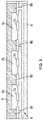
- FIG. 5is a side view of example EMI shield 64 connected to example DIB 50 .
- the EMI shieldis not part of the underlying DIB; that is, the EMI shield is not integrated into, or formed with, the DIB. Rather, the shield can be added to, or removed from, the DIB, using appropriate tools.
- the EMI shieldmay be reused on circuit boards having a surface trace configuration that matches, in whole or part, the configuration of the indentations on the conductive surface of the EMI shield.
- the EMI shieldmay be connected to the DIB using one or more removable bars across the cover that are configured to be tightened to attach the EMI shield to the surface of the DIB.
- the EMI shieldmay be connected to the DIB using one or more removable screws. For example, FIG. 4 shows four screw holes 81 for attaching the EMI shield to the DIB.
- the coverincludes three indentations, with one of the indentations defining a volume over conductive trace 51 a and with others of the indentations defining other volumes over the other conductive traces.
- the volumesthus include a first volume 65 a for first conductive trace 51 a , a different second volume 65 b for second conductive trace 51 b , and a different third volume 65 c for third conductive trace 51 c .
- each volumeis fully or partially electromagnetically isolated from the other volumes and each trace 51 a , 51 b , and 51 c is exposed to air in respective volumes 65 a , 65 b , and 65 c .
- the contactsinclude a first contact 66 a on a side of the indentation defining volume 65 a , a second contact 66 b on a side of the indentation defining volume 65 c , and contacts 66 c and 66 d between indentations and between the other two contacts 66 a and 66 b .
- the contactsconnect electrically to an electrical ground plane 68 in the DIB.
- the volumesare air-tight, whereas in other implementations the volumes are not air-tight.
- each conductive tracemay be shielded in a separate volume, as shown in FIG. 5 . This may reduce the chances of crosstalk or other electromagnetic interference between adjacent conductive traces.
- conductive traces that carry differential signalsare shielded in the same volume. For example, as shown in FIG. 6 , in EMI shield 69 , differential signal pair 70 is shielded within volume 71 and differential signal pair 72 is shielded within volume 73 .
- the remaining features of the DIB and the EMI shieldare the same as, or substantially the same as, the features described with respect to FIGS. 1 to 5 .
- the EMI shield and the indentationsmay have any appropriate sizes and shapes.
- a volume created by an indentation over a conductive tracehas a lateral width that is between 3 mils (76.2 microns) and 30 mils (762 microns) inclusive (e.g., 5 mils (126 microns)).
- at least two of multiple volumes created by the EMI shield over different tracesare separated by 78 mils (1981.2 microns) or less at a point on the DIB where the DUT connects to the DIB.
- a conductive plate having micro-machined grooves or channelscreates shielding and/or an impedance structure to surface traces, which are single-ended or differential, on a printed circuit board (PCB).
- the platemay be mechanically attached to the PCB's outer layers. The added shielding that the plate provides will enable signals to be brought closer together at faster speeds.
- test systems and processes described in this specification and their various modificationsmay be configured or controlled at least in part by one or more computers such as host computing system 12 using one or more computer programs tangibly embodied in one or more information carriers, such as in one or more non-transitory machine-readable storage media.
- a computer programcan be written in any form of programming language, including compiled or interpreted languages, and it can be deployed in any form, including as a stand-alone program or as a module, part, subroutine, or other unit suitable for use in a computing environment.
- a computer programcan be deployed to be executed on one computer or on multiple computers at one site or distributed across multiple sites and interconnected by a network.
- Actions associated with configuring or controlling the test systems and processescan be performed by one or more programmable processors executing one or more computer programs to control all or some of the well formation operations described previously. All or part of the test systems and processes can be configured or controlled by special purpose logic circuitry, such as, an FPGA (field programmable gate array) and/or an ASIC (application-specific integrated circuit).
- special purpose logic circuitrysuch as, an FPGA (field programmable gate array) and/or an ASIC (application-specific integrated circuit).
- processors suitable for the execution of a computer programinclude, by way of example, both general and special purpose microprocessors, and any one or more processors of any kind of digital computer.
- a processorwill receive instructions and data from a read-only storage area or a random access storage area or both.
- Elements of a computerinclude one or more processors for executing instructions and one or more storage area devices for storing instructions and data.
- a computerwill also include, or be operatively coupled to receive data from, or transfer data to, or both, one or more machine-readable storage media, such as mass storage devices for storing data, such as magnetic, magneto-optical disks, or optical disks.
- Non-transitory machine-readable storage media suitable for embodying computer program instructions and datainclude all forms of non-volatile storage area, including by way of example, semiconductor storage area devices, such as EPROM (erasable programmable read-only memory), EEPROM (electrically erasable programmable read-only memory), and flash storage area devices; magnetic disks, such as internal hard disks or removable disks; magneto-optical disks; and CD-ROM (compact disc read-only memory) and DVD-ROM (digital versatile disc read-only memory).
- semiconductor storage area devicessuch as EPROM (erasable programmable read-only memory), EEPROM (electrically erasable programmable read-only memory), and flash storage area devices
- magnetic diskssuch as internal hard disks or removable disks
- magneto-optical disksmagneto-optical disks
- CD-ROMcompact disc read-only memory
- DVD-ROMdigital versatile disc read-only memory
Landscapes
- Engineering & Computer Science (AREA)
- Physics & Mathematics (AREA)
- Microelectronics & Electronic Packaging (AREA)
- Electromagnetism (AREA)
- General Physics & Mathematics (AREA)
- General Engineering & Computer Science (AREA)
- Manufacturing & Machinery (AREA)
- Computer Hardware Design (AREA)
- Shielding Devices Or Components To Electric Or Magnetic Fields (AREA)
Abstract
Description
Claims (26)
Priority Applications (4)
| Application Number | Priority Date | Filing Date | Title |
|---|---|---|---|
| US16/563,143US11363746B2 (en) | 2019-09-06 | 2019-09-06 | EMI shielding for a signal trace |
| KR1020227009544AKR20220054622A (en) | 2019-09-06 | 2020-09-01 | EMI shielding for signal trace |
| CN202080060099.8ACN114286943A (en) | 2019-09-06 | 2020-09-01 | EMI shielding for signal traces |
| PCT/US2020/048933WO2021046049A1 (en) | 2019-09-06 | 2020-09-01 | Emi shielding for a signal trace |
Applications Claiming Priority (1)
| Application Number | Priority Date | Filing Date | Title |
|---|---|---|---|
| US16/563,143US11363746B2 (en) | 2019-09-06 | 2019-09-06 | EMI shielding for a signal trace |
Publications (2)
| Publication Number | Publication Date |
|---|---|
| US20210076546A1 US20210076546A1 (en) | 2021-03-11 |
| US11363746B2true US11363746B2 (en) | 2022-06-14 |
Family
ID=74849681
Family Applications (1)
| Application Number | Title | Priority Date | Filing Date |
|---|---|---|---|
| US16/563,143Active2040-03-31US11363746B2 (en) | 2019-09-06 | 2019-09-06 | EMI shielding for a signal trace |
Country Status (4)
| Country | Link |
|---|---|
| US (1) | US11363746B2 (en) |
| KR (1) | KR20220054622A (en) |
| CN (1) | CN114286943A (en) |
| WO (1) | WO2021046049A1 (en) |
Citations (104)
| Publication number | Priority date | Publication date | Assignee | Title |
|---|---|---|---|---|
| US3516077A (en) | 1968-05-28 | 1970-06-02 | Bell Telephone Labor Inc | Magnetic propagation device wherein pole patterns move along the periphery of magnetic disks |
| US3577131A (en) | 1969-01-30 | 1971-05-04 | Bell Telephone Labor Inc | Domain propagation arrangement |
| US3673433A (en) | 1970-08-21 | 1972-06-27 | Siemens Ag Albis | Circuit arrangement for selectively connecting at least two inputs to a counting stage possessing at least one preparatory input and one triggering input and including contact bounce suppression circuitry |
| US3934236A (en) | 1974-01-11 | 1976-01-20 | Monsanto Company | Pulsed field accessed bubble propagation circuits |
| US4021790A (en) | 1974-01-11 | 1977-05-03 | Monsanto Company | Mutually exclusive magnetic bubble propagation circuits |
| US4117543A (en) | 1972-08-24 | 1978-09-26 | Monsanto Company | Magnetic bubble logic family |
| US4692839A (en) | 1985-06-24 | 1987-09-08 | Digital Equipment Corporation | Multiple chip interconnection system and package |
| US4729166A (en) | 1985-07-22 | 1988-03-08 | Digital Equipment Corporation | Method of fabricating electrical connector for surface mounting |
| US4754546A (en) | 1985-07-22 | 1988-07-05 | Digital Equipment Corporation | Electrical connector for surface mounting and method of making thereof |
| US4757256A (en) | 1985-05-10 | 1988-07-12 | Micro-Probe, Inc. | High density probe card |
| US4758785A (en) | 1986-09-03 | 1988-07-19 | Tektronix, Inc. | Pressure control apparatus for use in an integrated circuit testing station |
| WO1988005544A1 (en) | 1987-01-20 | 1988-07-28 | Hughes Aircraft Company | Test connector for electrical devices |
| US4778950A (en) | 1985-07-22 | 1988-10-18 | Digital Equipment Corporation | Anisotropic elastomeric interconnecting system |
| EP0298219A2 (en) | 1987-06-08 | 1989-01-11 | Tektronix Inc. | Method and apparatus for testing unpackaged integrated circuits in a hybrid circuit environment |
| US4804132A (en) | 1987-08-28 | 1989-02-14 | Difrancesco Louis | Method for cold bonding |
| US4912399A (en) | 1987-06-09 | 1990-03-27 | Tektronix, Inc. | Multiple lead probe for integrated circuits in wafer form |
| EP0361779A1 (en) | 1988-09-26 | 1990-04-04 | Hewlett-Packard Company | Micro-strip architecture for membrane test probe |
| US4918383A (en) | 1987-01-20 | 1990-04-17 | Huff Richard E | Membrane probe with automatic contact scrub action |
| US4922192A (en) | 1988-09-06 | 1990-05-01 | Unisys Corporation | Elastic membrane probe |
| US4954873A (en) | 1985-07-22 | 1990-09-04 | Digital Equipment Corporation | Electrical connector for surface mounting |
| US4975638A (en) | 1989-12-18 | 1990-12-04 | Wentworth Laboratories | Test probe assembly for testing integrated circuit devices |
| US4980637A (en) | 1988-03-01 | 1990-12-25 | Hewlett-Packard Company | Force delivery system for improved precision membrane probe |
| US5020219A (en) | 1988-05-16 | 1991-06-04 | Leedy Glenn J | Method of making a flexible tester surface for testing integrated circuits |
| US5072176A (en) | 1990-07-10 | 1991-12-10 | The United States Of America As Represented By The Secretary Of The Army | Flexible membrane circuit tester |
| US5083697A (en) | 1990-02-14 | 1992-01-28 | Difrancesco Louis | Particle-enhanced joining of metal surfaces |
| US5105557A (en) | 1991-03-11 | 1992-04-21 | Vadasz Jozsef T | System for rapidly drying parts |
| US5132613A (en) | 1990-11-30 | 1992-07-21 | International Business Machines Corporation | Low inductance side mount decoupling test structure |
| US5180977A (en) | 1991-12-02 | 1993-01-19 | Hoya Corporation Usa | Membrane probe contact bump compliancy system |
| US5264787A (en) | 1991-08-30 | 1993-11-23 | Hughes Aircraft Company | Rigid-flex circuits with raised features as IC test probes |
| US5355079A (en) | 1993-01-07 | 1994-10-11 | Wentworth Laboratories, Inc. | Probe assembly for testing integrated circuit devices |
| US5378982A (en) | 1993-02-25 | 1995-01-03 | Hughes Aircraft Company | Test probe for panel having an overlying protective member adjacent panel contacts |
| US5416429A (en) | 1994-05-23 | 1995-05-16 | Wentworth Laboratories, Inc. | Probe assembly for testing integrated circuits |
| US5422574A (en) | 1993-01-14 | 1995-06-06 | Probe Technology Corporation | Large scale protrusion membrane for semiconductor devices under test with very high pin counts |
| US5456404A (en) | 1993-10-28 | 1995-10-10 | Digital Equipment Corporation | Method of testing semiconductor chips with reusable test package |
| US5469072A (en) | 1993-11-01 | 1995-11-21 | Motorola, Inc. | Integrated circuit test system |
| US5468157A (en) | 1993-10-29 | 1995-11-21 | Texas Instruments Incorporated | Non-destructive interconnect system for semiconductor devices |
| US5623213A (en) | 1994-09-09 | 1997-04-22 | Micromodule Systems | Membrane probing of circuits |
| US5914613A (en) | 1996-08-08 | 1999-06-22 | Cascade Microtech, Inc. | Membrane probing system with local contact scrub |
| US5968282A (en) | 1997-11-10 | 1999-10-19 | Tokyo Electron Limited | Mechanism and method for cleaning probe needles |
| US5973405A (en) | 1997-07-22 | 1999-10-26 | Dytak Corporation | Composite electrical contact structure and method for manufacturing the same |
| US6246245B1 (en) | 1998-02-23 | 2001-06-12 | Micron Technology, Inc. | Probe card, test method and test system for semiconductor wafers |
| US6256882B1 (en) | 1998-07-14 | 2001-07-10 | Cascade Microtech, Inc. | Membrane probing system |
| US6444922B1 (en) | 1999-11-18 | 2002-09-03 | Nortel Networks Limited | Zero cross-talk signal line design |
| US6494734B1 (en) | 1997-09-30 | 2002-12-17 | Fci Americas Technology, Inc. | High density electrical connector assembly |
| US6499216B1 (en) | 1994-07-07 | 2002-12-31 | Tessera, Inc. | Methods and structures for electronic probing arrays |
| US6566898B2 (en) | 2000-03-06 | 2003-05-20 | Wentworth Laboratories, Inc. | Temperature compensated vertical pin probing device |
| US6578264B1 (en) | 1999-06-04 | 2003-06-17 | Cascade Microtech, Inc. | Method for constructing a membrane probe using a depression |
| US6586955B2 (en) | 2000-03-13 | 2003-07-01 | Tessera, Inc. | Methods and structures for electronic probing arrays |
| US20030122538A1 (en) | 2000-09-28 | 2003-07-03 | Teradyne, Inc. | Coaxial cable for ATE with overvoltage protection |
| US6633175B1 (en) | 2000-03-06 | 2003-10-14 | Wenworth Laboratories, Inc. | Temperature compensated vertical pin probing device |
| US6661244B2 (en) | 2000-03-06 | 2003-12-09 | Wentworth Laboratories, Inc. | Nickel alloy probe card frame laminate |
| US6690186B2 (en) | 1994-07-07 | 2004-02-10 | Tessera, Inc. | Methods and structures for electronic probing arrays |
| US6756797B2 (en) | 2001-01-31 | 2004-06-29 | Wentworth Laboratories Inc. | Planarizing interposer for thermal compensation of a probe card |
| US6838890B2 (en) | 2000-02-25 | 2005-01-04 | Cascade Microtech, Inc. | Membrane probing system |
| US6911835B2 (en) | 2002-05-08 | 2005-06-28 | Formfactor, Inc. | High performance probe system |
| US6927586B2 (en) | 2000-03-06 | 2005-08-09 | Wentworth Laboratories, Inc. | Temperature compensated vertical pin probing device |
| US20050223543A1 (en) | 2003-12-31 | 2005-10-13 | Microfabrica Inc. | Electrochemical fabrication method for fabricating space transformers or co-fabricating probes and space transformers |
| US6965244B2 (en) | 2002-05-08 | 2005-11-15 | Formfactor, Inc. | High performance probe system |
| US20060124927A1 (en) | 2004-12-09 | 2006-06-15 | International Business Machines Corporation | Forming of high aspect ratio conductive structure using injection molded solder |
| US7084657B2 (en) | 1998-06-09 | 2006-08-01 | Advantest Corporation | Bump and method of forming bump |
| US20060272856A1 (en) | 2003-06-19 | 2006-12-07 | Wavezero, Inc. | Emi absorbing shielding for a printed circuit board |
| US7161363B2 (en) | 2002-05-23 | 2007-01-09 | Cascade Microtech, Inc. | Probe for testing a device under test |
| US7233160B2 (en) | 2000-12-04 | 2007-06-19 | Cascade Microtech, Inc. | Wafer probe |
| US7271603B2 (en) | 2003-05-23 | 2007-09-18 | Cascade Microtech, Inc. | Shielded probe for testing a device under test |
| US7285969B2 (en) | 2002-11-13 | 2007-10-23 | Cascade Microtech, Inc. | Probe for combined signals |
| US20080061808A1 (en) | 2006-09-12 | 2008-03-13 | Sammy Mok | Compliance partitioning in testing of integrated circuits |
| US7355420B2 (en) | 2001-08-21 | 2008-04-08 | Cascade Microtech, Inc. | Membrane probing system |
| US20080100323A1 (en) | 2006-10-25 | 2008-05-01 | Silicon Test Systems, Inc. | Low cost, high pin count, wafer sort automated test equipment (ate) device under test (dut) interface for testing electronic devices in high parallelism |
| US7368927B2 (en) | 2004-07-07 | 2008-05-06 | Cascade Microtech, Inc. | Probe head having a membrane suspended probe |
| US7403028B2 (en) | 2006-06-12 | 2008-07-22 | Cascade Microtech, Inc. | Test structure and probe for differential signals |
| US7420381B2 (en) | 2004-09-13 | 2008-09-02 | Cascade Microtech, Inc. | Double sided probing structures |
| US7427868B2 (en) | 2003-12-24 | 2008-09-23 | Cascade Microtech, Inc. | Active wafer probe |
| US7443186B2 (en) | 2006-06-12 | 2008-10-28 | Cascade Microtech, Inc. | On-wafer test structures for differential signals |
| US20080265919A1 (en) | 2007-04-02 | 2008-10-30 | Izadian Jamal S | Scalable wideband probes, fixtures, and sockets for high speed ic testing and interconnects |
| US7449899B2 (en) | 2005-06-08 | 2008-11-11 | Cascade Microtech, Inc. | Probe for high frequency signals |
| US7453275B2 (en) | 2006-05-19 | 2008-11-18 | Elpida Memory, Inc. | Probe card |
| US7504842B2 (en) | 1997-05-28 | 2009-03-17 | Cascade Microtech, Inc. | Probe holder for testing of a test device |
| US7535247B2 (en) | 2005-01-31 | 2009-05-19 | Cascade Microtech, Inc. | Interface for testing semiconductors |
| US7601039B2 (en) | 1993-11-16 | 2009-10-13 | Formfactor, Inc. | Microelectronic contact structure and method of making same |
| US7609077B2 (en) | 2006-06-09 | 2009-10-27 | Cascade Microtech, Inc. | Differential signal probe with integral balun |
| US7619419B2 (en) | 2005-06-13 | 2009-11-17 | Cascade Microtech, Inc. | Wideband active-passive differential signal probe |
| US7656172B2 (en) | 2005-01-31 | 2010-02-02 | Cascade Microtech, Inc. | System for testing semiconductors |
| US7723999B2 (en) | 2006-06-12 | 2010-05-25 | Cascade Microtech, Inc. | Calibration structures for differential signal probing |
| US7764072B2 (en) | 2006-06-12 | 2010-07-27 | Cascade Microtech, Inc. | Differential signal probing system |
| US7791361B2 (en) | 2007-12-10 | 2010-09-07 | Touchdown Technologies, Inc. | Planarizing probe card |
| US7800001B2 (en) | 2006-04-14 | 2010-09-21 | Kabushiki Kaisha Nihon Micronics | Probe sheet and electrical connecting apparatus |
| US7876114B2 (en) | 2007-08-08 | 2011-01-25 | Cascade Microtech, Inc. | Differential waveguide probe |
| US7888957B2 (en) | 2008-10-06 | 2011-02-15 | Cascade Microtech, Inc. | Probing apparatus with impedance optimized interface |
| US20110095778A1 (en) | 2009-10-28 | 2011-04-28 | Young Huang Chou | Probe card |
| US7934944B2 (en) | 2006-04-07 | 2011-05-03 | Kabushiki Kaisha Nihon Micronics | Electrical connecting apparatus |
| US7934945B2 (en) | 2006-09-28 | 2011-05-03 | Kabushiki Kaisha Nihon Micronics | Electrical connecting apparatus |
| US20110133738A1 (en)* | 2009-12-07 | 2011-06-09 | Abbink Henry C | Systems and Methods for Obstructing Magnetic Flux |
| US8033838B2 (en) | 1996-02-21 | 2011-10-11 | Formfactor, Inc. | Microelectronic contact structure |
| US20120017428A1 (en) | 2008-03-07 | 2012-01-26 | Taiwan Semiconductor Manufacturing Co., Ltd. | Method for fabricating a semiconductor test probe card space transformer |
| US20120034820A1 (en) | 2009-02-18 | 2012-02-09 | Molex Incorporated | Vertical connector for a printed circuit board |
| US8202684B2 (en) | 2006-04-14 | 2012-06-19 | Kabushiki Kaisha Nihon Micronics | Method for manufacturing probe sheet |
| US20120175612A1 (en) | 2009-09-25 | 2012-07-12 | International Business Machines Corporation | Test structure for determination of tsv depth |
| US8373428B2 (en) | 1993-11-16 | 2013-02-12 | Formfactor, Inc. | Probe card assembly and kit, and methods of making same |
| US8410806B2 (en) | 2008-11-21 | 2013-04-02 | Cascade Microtech, Inc. | Replaceable coupon for a probing apparatus |
| WO2013134568A1 (en) | 2012-03-07 | 2013-09-12 | Advantest Corporation | Shielded probe array |
| US20140253109A1 (en)* | 2013-03-08 | 2014-09-11 | Deere & Company | Method and sensor for sensing current in a conductor |
| US20150091594A1 (en)* | 2013-06-24 | 2015-04-02 | The United States Of America As Represented By The Secretary Of The Navy | Apparatus and Method for Integrated Circuit Forensics |
| US9435855B2 (en) | 2013-11-19 | 2016-09-06 | Teradyne, Inc. | Interconnect for transmitting signals between a device and a tester |
| WO2019152762A1 (en) | 2018-02-01 | 2019-08-08 | Henkel IP & Holding GmbH | Method for shielding system-in-package assemblies from electromagnetic interference |
Family Cites Families (8)
| Publication number | Priority date | Publication date | Assignee | Title |
|---|---|---|---|---|
| JP2007258391A (en)* | 2006-03-23 | 2007-10-04 | Tdk Corp | Shield structure of circuit board |
| CN101433132B (en)* | 2006-05-02 | 2012-07-04 | 富多电子公司 | Shielded flexible circuit, method for forming same, and flexible cable |
| CN201352456Y (en)* | 2008-12-17 | 2009-11-25 | 深圳易拓科技有限公司 | Electromagnetic shielding cover of mobile hard disk and mobile hard disk |
| US8213180B2 (en)* | 2010-01-21 | 2012-07-03 | Broadcom Corporation | Electromagnetic interference shield with integrated heat sink |
| CN101983003B (en)* | 2010-08-31 | 2014-04-02 | 华为终端有限公司 | Circuit board |
| CN202059725U (en)* | 2011-05-12 | 2011-11-30 | 康佳集团股份有限公司 | Electromagnetic compatibility (EMC) shielding device |
| CN107771021A (en)* | 2017-09-26 | 2018-03-06 | 广东欧珀移动通信有限公司 | Mobile terminal, circuit board assembly and shielding case thereof |
| US10468355B2 (en)* | 2017-12-08 | 2019-11-05 | Taiwan Semiconductor Manufacturing Company, Ltd. | EMI Shielding structure in InFO package |
- 2019
- 2019-09-06USUS16/563,143patent/US11363746B2/enactiveActive
- 2020
- 2020-09-01KRKR1020227009544Apatent/KR20220054622A/enactivePending
- 2020-09-01CNCN202080060099.8Apatent/CN114286943A/enactivePending
- 2020-09-01WOPCT/US2020/048933patent/WO2021046049A1/ennot_activeCeased
Patent Citations (149)
| Publication number | Priority date | Publication date | Assignee | Title |
|---|---|---|---|---|
| US3516077A (en) | 1968-05-28 | 1970-06-02 | Bell Telephone Labor Inc | Magnetic propagation device wherein pole patterns move along the periphery of magnetic disks |
| US3577131A (en) | 1969-01-30 | 1971-05-04 | Bell Telephone Labor Inc | Domain propagation arrangement |
| US3673433A (en) | 1970-08-21 | 1972-06-27 | Siemens Ag Albis | Circuit arrangement for selectively connecting at least two inputs to a counting stage possessing at least one preparatory input and one triggering input and including contact bounce suppression circuitry |
| US4117543A (en) | 1972-08-24 | 1978-09-26 | Monsanto Company | Magnetic bubble logic family |
| US3934236A (en) | 1974-01-11 | 1976-01-20 | Monsanto Company | Pulsed field accessed bubble propagation circuits |
| US4021790A (en) | 1974-01-11 | 1977-05-03 | Monsanto Company | Mutually exclusive magnetic bubble propagation circuits |
| US4757256A (en) | 1985-05-10 | 1988-07-12 | Micro-Probe, Inc. | High density probe card |
| US4692839A (en) | 1985-06-24 | 1987-09-08 | Digital Equipment Corporation | Multiple chip interconnection system and package |
| US4778950A (en) | 1985-07-22 | 1988-10-18 | Digital Equipment Corporation | Anisotropic elastomeric interconnecting system |
| US4729166A (en) | 1985-07-22 | 1988-03-08 | Digital Equipment Corporation | Method of fabricating electrical connector for surface mounting |
| US4754546A (en) | 1985-07-22 | 1988-07-05 | Digital Equipment Corporation | Electrical connector for surface mounting and method of making thereof |
| US4954873A (en) | 1985-07-22 | 1990-09-04 | Digital Equipment Corporation | Electrical connector for surface mounting |
| US4758785A (en) | 1986-09-03 | 1988-07-19 | Tektronix, Inc. | Pressure control apparatus for use in an integrated circuit testing station |
| US4918383A (en) | 1987-01-20 | 1990-04-17 | Huff Richard E | Membrane probe with automatic contact scrub action |
| WO1988005544A1 (en) | 1987-01-20 | 1988-07-28 | Hughes Aircraft Company | Test connector for electrical devices |
| EP0298219A2 (en) | 1987-06-08 | 1989-01-11 | Tektronix Inc. | Method and apparatus for testing unpackaged integrated circuits in a hybrid circuit environment |
| US4912399A (en) | 1987-06-09 | 1990-03-27 | Tektronix, Inc. | Multiple lead probe for integrated circuits in wafer form |
| US4804132A (en) | 1987-08-28 | 1989-02-14 | Difrancesco Louis | Method for cold bonding |
| US4980637A (en) | 1988-03-01 | 1990-12-25 | Hewlett-Packard Company | Force delivery system for improved precision membrane probe |
| US5020219A (en) | 1988-05-16 | 1991-06-04 | Leedy Glenn J | Method of making a flexible tester surface for testing integrated circuits |
| US4922192A (en) | 1988-09-06 | 1990-05-01 | Unisys Corporation | Elastic membrane probe |
| EP0361779A1 (en) | 1988-09-26 | 1990-04-04 | Hewlett-Packard Company | Micro-strip architecture for membrane test probe |
| US4975638A (en) | 1989-12-18 | 1990-12-04 | Wentworth Laboratories | Test probe assembly for testing integrated circuit devices |
| US5083697A (en) | 1990-02-14 | 1992-01-28 | Difrancesco Louis | Particle-enhanced joining of metal surfaces |
| US5072176A (en) | 1990-07-10 | 1991-12-10 | The United States Of America As Represented By The Secretary Of The Army | Flexible membrane circuit tester |
| US5132613A (en) | 1990-11-30 | 1992-07-21 | International Business Machines Corporation | Low inductance side mount decoupling test structure |
| US5105557A (en) | 1991-03-11 | 1992-04-21 | Vadasz Jozsef T | System for rapidly drying parts |
| US5264787A (en) | 1991-08-30 | 1993-11-23 | Hughes Aircraft Company | Rigid-flex circuits with raised features as IC test probes |
| US5180977A (en) | 1991-12-02 | 1993-01-19 | Hoya Corporation Usa | Membrane probe contact bump compliancy system |
| US5355079A (en) | 1993-01-07 | 1994-10-11 | Wentworth Laboratories, Inc. | Probe assembly for testing integrated circuit devices |
| US5422574A (en) | 1993-01-14 | 1995-06-06 | Probe Technology Corporation | Large scale protrusion membrane for semiconductor devices under test with very high pin counts |
| US5378982A (en) | 1993-02-25 | 1995-01-03 | Hughes Aircraft Company | Test probe for panel having an overlying protective member adjacent panel contacts |
| US5456404A (en) | 1993-10-28 | 1995-10-10 | Digital Equipment Corporation | Method of testing semiconductor chips with reusable test package |
| US5468157A (en) | 1993-10-29 | 1995-11-21 | Texas Instruments Incorporated | Non-destructive interconnect system for semiconductor devices |
| US5469072A (en) | 1993-11-01 | 1995-11-21 | Motorola, Inc. | Integrated circuit test system |
| US8373428B2 (en) | 1993-11-16 | 2013-02-12 | Formfactor, Inc. | Probe card assembly and kit, and methods of making same |
| US7601039B2 (en) | 1993-11-16 | 2009-10-13 | Formfactor, Inc. | Microelectronic contact structure and method of making same |
| US5416429A (en) | 1994-05-23 | 1995-05-16 | Wentworth Laboratories, Inc. | Probe assembly for testing integrated circuits |
| US6499216B1 (en) | 1994-07-07 | 2002-12-31 | Tessera, Inc. | Methods and structures for electronic probing arrays |
| US6690186B2 (en) | 1994-07-07 | 2004-02-10 | Tessera, Inc. | Methods and structures for electronic probing arrays |
| US5623213A (en) | 1994-09-09 | 1997-04-22 | Micromodule Systems | Membrane probing of circuits |
| US8033838B2 (en) | 1996-02-21 | 2011-10-11 | Formfactor, Inc. | Microelectronic contact structure |
| US6437584B1 (en) | 1996-08-08 | 2002-08-20 | Cascade Microtech, Inc. | Membrane probing system with local contact scrub |
| US7541821B2 (en) | 1996-08-08 | 2009-06-02 | Cascade Microtech, Inc. | Membrane probing system with local contact scrub |
| US6307387B1 (en) | 1996-08-08 | 2001-10-23 | Cascade Microtech, Inc. | Membrane probing system with local contact scrub |
| US7109731B2 (en) | 1996-08-08 | 2006-09-19 | Cascade Microtech, Inc. | Membrane probing system with local contact scrub |
| US7893704B2 (en) | 1996-08-08 | 2011-02-22 | Cascade Microtech, Inc. | Membrane probing structure with laterally scrubbing contacts |
| US6927585B2 (en) | 1996-08-08 | 2005-08-09 | Cascade Microtech, Inc. | Membrane probing system with local contact scrub |
| US5914613A (en) | 1996-08-08 | 1999-06-22 | Cascade Microtech, Inc. | Membrane probing system with local contact scrub |
| US7504842B2 (en) | 1997-05-28 | 2009-03-17 | Cascade Microtech, Inc. | Probe holder for testing of a test device |
| US6359337B1 (en) | 1997-07-22 | 2002-03-19 | Dytak Corporation | Composite electrical contact structure and method for manufacturing the same |
| US5973405A (en) | 1997-07-22 | 1999-10-26 | Dytak Corporation | Composite electrical contact structure and method for manufacturing the same |
| US6494734B1 (en) | 1997-09-30 | 2002-12-17 | Fci Americas Technology, Inc. | High density electrical connector assembly |
| US5968282A (en) | 1997-11-10 | 1999-10-19 | Tokyo Electron Limited | Mechanism and method for cleaning probe needles |
| US6246245B1 (en) | 1998-02-23 | 2001-06-12 | Micron Technology, Inc. | Probe card, test method and test system for semiconductor wafers |
| US6356098B1 (en) | 1998-02-23 | 2002-03-12 | Micron Technology, Inc. | Probe card, test method and test system for semiconductor wafers |
| US7084657B2 (en) | 1998-06-09 | 2006-08-01 | Advantest Corporation | Bump and method of forming bump |
| US7761986B2 (en) | 1998-07-14 | 2010-07-27 | Cascade Microtech, Inc. | Membrane probing method using improved contact |
| US6708386B2 (en) | 1998-07-14 | 2004-03-23 | Cascade Microtech, Inc. | Method for probing an electrical device having a layer of oxide thereon |
| US8451017B2 (en) | 1998-07-14 | 2013-05-28 | Cascade Microtech, Inc. | Membrane probing method using improved contact |
| US6825677B2 (en) | 1998-07-14 | 2004-11-30 | Cascade Microtech, Inc. | Membrane probing system |
| US7400155B2 (en) | 1998-07-14 | 2008-07-15 | Cascade Microtech, Inc. | Membrane probing system |
| US6860009B2 (en) | 1998-07-14 | 2005-03-01 | Cascade Microtech, Inc. | Probe construction using a recess |
| US7266889B2 (en) | 1998-07-14 | 2007-09-11 | Cascade Microtech, Inc. | Membrane probing system |
| US6256882B1 (en) | 1998-07-14 | 2001-07-10 | Cascade Microtech, Inc. | Membrane probing system |
| US7681312B2 (en) | 1998-07-14 | 2010-03-23 | Cascade Microtech, Inc. | Membrane probing system |
| US7178236B2 (en) | 1999-06-04 | 2007-02-20 | Cascade Microtech, Inc. | Method for constructing a membrane probe using a depression |
| US7533462B2 (en) | 1999-06-04 | 2009-05-19 | Cascade Microtech, Inc. | Method of constructing a membrane probe |
| US6578264B1 (en) | 1999-06-04 | 2003-06-17 | Cascade Microtech, Inc. | Method for constructing a membrane probe using a depression |
| US6444922B1 (en) | 1999-11-18 | 2002-09-03 | Nortel Networks Limited | Zero cross-talk signal line design |
| US7403025B2 (en) | 2000-02-25 | 2008-07-22 | Cascade Microtech, Inc. | Membrane probing system |
| US6838890B2 (en) | 2000-02-25 | 2005-01-04 | Cascade Microtech, Inc. | Membrane probing system |
| US6930498B2 (en) | 2000-02-25 | 2005-08-16 | Cascade Microtech, Inc. | Membrane probing system |
| US7148711B2 (en) | 2000-02-25 | 2006-12-12 | Cascade Microtech, Inc. | Membrane probing system |
| US6661244B2 (en) | 2000-03-06 | 2003-12-09 | Wentworth Laboratories, Inc. | Nickel alloy probe card frame laminate |
| US6633175B1 (en) | 2000-03-06 | 2003-10-14 | Wenworth Laboratories, Inc. | Temperature compensated vertical pin probing device |
| US6927586B2 (en) | 2000-03-06 | 2005-08-09 | Wentworth Laboratories, Inc. | Temperature compensated vertical pin probing device |
| US6566898B2 (en) | 2000-03-06 | 2003-05-20 | Wentworth Laboratories, Inc. | Temperature compensated vertical pin probing device |
| US6586955B2 (en) | 2000-03-13 | 2003-07-01 | Tessera, Inc. | Methods and structures for electronic probing arrays |
| US20030122538A1 (en) | 2000-09-28 | 2003-07-03 | Teradyne, Inc. | Coaxial cable for ATE with overvoltage protection |
| US7233160B2 (en) | 2000-12-04 | 2007-06-19 | Cascade Microtech, Inc. | Wafer probe |
| US7495461B2 (en) | 2000-12-04 | 2009-02-24 | Cascade Microtech, Inc. | Wafer probe |
| US7456646B2 (en) | 2000-12-04 | 2008-11-25 | Cascade Microtech, Inc. | Wafer probe |
| US7761983B2 (en) | 2000-12-04 | 2010-07-27 | Cascade Microtech, Inc. | Method of assembling a wafer probe |
| US7688097B2 (en) | 2000-12-04 | 2010-03-30 | Cascade Microtech, Inc. | Wafer probe |
| US6756797B2 (en) | 2001-01-31 | 2004-06-29 | Wentworth Laboratories Inc. | Planarizing interposer for thermal compensation of a probe card |
| US7355420B2 (en) | 2001-08-21 | 2008-04-08 | Cascade Microtech, Inc. | Membrane probing system |
| US7492175B2 (en) | 2001-08-21 | 2009-02-17 | Cascade Microtech, Inc. | Membrane probing system |
| US6911835B2 (en) | 2002-05-08 | 2005-06-28 | Formfactor, Inc. | High performance probe system |
| US6965244B2 (en) | 2002-05-08 | 2005-11-15 | Formfactor, Inc. | High performance probe system |
| US7764075B2 (en) | 2002-05-08 | 2010-07-27 | Formfactor, Inc. | High performance probe system |
| US7227371B2 (en) | 2002-05-08 | 2007-06-05 | Formfactor, Inc. | High performance probe system |
| US7443181B2 (en) | 2002-05-08 | 2008-10-28 | Formfactor, Inc. | High performance probe system |
| US7489149B2 (en) | 2002-05-23 | 2009-02-10 | Cascade Microtech, Inc. | Shielded probe for testing a device under test |
| US7161363B2 (en) | 2002-05-23 | 2007-01-09 | Cascade Microtech, Inc. | Probe for testing a device under test |
| US7436194B2 (en) | 2002-05-23 | 2008-10-14 | Cascade Microtech, Inc. | Shielded probe with low contact resistance for testing a device under test |
| US7482823B2 (en) | 2002-05-23 | 2009-01-27 | Cascade Microtech, Inc. | Shielded probe for testing a device under test |
| US7518387B2 (en) | 2002-05-23 | 2009-04-14 | Cascade Microtech, Inc. | Shielded probe for testing a device under test |
| US7304488B2 (en) | 2002-05-23 | 2007-12-04 | Cascade Microtech, Inc. | Shielded probe for high-frequency testing of a device under test |
| US7453276B2 (en) | 2002-11-13 | 2008-11-18 | Cascade Microtech, Inc. | Probe for combined signals |
| US7417446B2 (en) | 2002-11-13 | 2008-08-26 | Cascade Microtech, Inc. | Probe for combined signals |
| US7285969B2 (en) | 2002-11-13 | 2007-10-23 | Cascade Microtech, Inc. | Probe for combined signals |
| US7898273B2 (en) | 2003-05-23 | 2011-03-01 | Cascade Microtech, Inc. | Probe for testing a device under test |
| US7498829B2 (en) | 2003-05-23 | 2009-03-03 | Cascade Microtech, Inc. | Shielded probe for testing a device under test |
| US7501842B2 (en) | 2003-05-23 | 2009-03-10 | Cascade Microtech, Inc. | Shielded probe for testing a device under test |
| US7271603B2 (en) | 2003-05-23 | 2007-09-18 | Cascade Microtech, Inc. | Shielded probe for testing a device under test |
| US20060272856A1 (en) | 2003-06-19 | 2006-12-07 | Wavezero, Inc. | Emi absorbing shielding for a printed circuit board |
| US7427868B2 (en) | 2003-12-24 | 2008-09-23 | Cascade Microtech, Inc. | Active wafer probe |
| US7759953B2 (en) | 2003-12-24 | 2010-07-20 | Cascade Microtech, Inc. | Active wafer probe |
| US20050223543A1 (en) | 2003-12-31 | 2005-10-13 | Microfabrica Inc. | Electrochemical fabrication method for fabricating space transformers or co-fabricating probes and space transformers |
| US7514944B2 (en) | 2004-07-07 | 2009-04-07 | Cascade Microtech, Inc. | Probe head having a membrane suspended probe |
| US7368927B2 (en) | 2004-07-07 | 2008-05-06 | Cascade Microtech, Inc. | Probe head having a membrane suspended probe |
| US8013623B2 (en) | 2004-09-13 | 2011-09-06 | Cascade Microtech, Inc. | Double sided probing structures |
| US7420381B2 (en) | 2004-09-13 | 2008-09-02 | Cascade Microtech, Inc. | Double sided probing structures |
| US20060124927A1 (en) | 2004-12-09 | 2006-06-15 | International Business Machines Corporation | Forming of high aspect ratio conductive structure using injection molded solder |
| US7656172B2 (en) | 2005-01-31 | 2010-02-02 | Cascade Microtech, Inc. | System for testing semiconductors |
| US7898281B2 (en) | 2005-01-31 | 2011-03-01 | Cascade Mircotech, Inc. | Interface for testing semiconductors |
| US7535247B2 (en) | 2005-01-31 | 2009-05-19 | Cascade Microtech, Inc. | Interface for testing semiconductors |
| US7940069B2 (en) | 2005-01-31 | 2011-05-10 | Cascade Microtech, Inc. | System for testing semiconductors |
| US7449899B2 (en) | 2005-06-08 | 2008-11-11 | Cascade Microtech, Inc. | Probe for high frequency signals |
| US7619419B2 (en) | 2005-06-13 | 2009-11-17 | Cascade Microtech, Inc. | Wideband active-passive differential signal probe |
| US7934944B2 (en) | 2006-04-07 | 2011-05-03 | Kabushiki Kaisha Nihon Micronics | Electrical connecting apparatus |
| US8202684B2 (en) | 2006-04-14 | 2012-06-19 | Kabushiki Kaisha Nihon Micronics | Method for manufacturing probe sheet |
| US7800001B2 (en) | 2006-04-14 | 2010-09-21 | Kabushiki Kaisha Nihon Micronics | Probe sheet and electrical connecting apparatus |
| US7453275B2 (en) | 2006-05-19 | 2008-11-18 | Elpida Memory, Inc. | Probe card |
| US7609077B2 (en) | 2006-06-09 | 2009-10-27 | Cascade Microtech, Inc. | Differential signal probe with integral balun |
| US7403028B2 (en) | 2006-06-12 | 2008-07-22 | Cascade Microtech, Inc. | Test structure and probe for differential signals |
| US7443186B2 (en) | 2006-06-12 | 2008-10-28 | Cascade Microtech, Inc. | On-wafer test structures for differential signals |
| US7764072B2 (en) | 2006-06-12 | 2010-07-27 | Cascade Microtech, Inc. | Differential signal probing system |
| US7750652B2 (en) | 2006-06-12 | 2010-07-06 | Cascade Microtech, Inc. | Test structure and probe for differential signals |
| US7723999B2 (en) | 2006-06-12 | 2010-05-25 | Cascade Microtech, Inc. | Calibration structures for differential signal probing |
| US20080061808A1 (en) | 2006-09-12 | 2008-03-13 | Sammy Mok | Compliance partitioning in testing of integrated circuits |
| US7934945B2 (en) | 2006-09-28 | 2011-05-03 | Kabushiki Kaisha Nihon Micronics | Electrical connecting apparatus |
| US20080100323A1 (en) | 2006-10-25 | 2008-05-01 | Silicon Test Systems, Inc. | Low cost, high pin count, wafer sort automated test equipment (ate) device under test (dut) interface for testing electronic devices in high parallelism |
| US20080265919A1 (en) | 2007-04-02 | 2008-10-30 | Izadian Jamal S | Scalable wideband probes, fixtures, and sockets for high speed ic testing and interconnects |
| US7876114B2 (en) | 2007-08-08 | 2011-01-25 | Cascade Microtech, Inc. | Differential waveguide probe |
| US7791361B2 (en) | 2007-12-10 | 2010-09-07 | Touchdown Technologies, Inc. | Planarizing probe card |
| US20120017428A1 (en) | 2008-03-07 | 2012-01-26 | Taiwan Semiconductor Manufacturing Co., Ltd. | Method for fabricating a semiconductor test probe card space transformer |
| US7888957B2 (en) | 2008-10-06 | 2011-02-15 | Cascade Microtech, Inc. | Probing apparatus with impedance optimized interface |
| US8410806B2 (en) | 2008-11-21 | 2013-04-02 | Cascade Microtech, Inc. | Replaceable coupon for a probing apparatus |
| US20120034820A1 (en) | 2009-02-18 | 2012-02-09 | Molex Incorporated | Vertical connector for a printed circuit board |
| US20120175612A1 (en) | 2009-09-25 | 2012-07-12 | International Business Machines Corporation | Test structure for determination of tsv depth |
| US20110095778A1 (en) | 2009-10-28 | 2011-04-28 | Young Huang Chou | Probe card |
| US20110133738A1 (en)* | 2009-12-07 | 2011-06-09 | Abbink Henry C | Systems and Methods for Obstructing Magnetic Flux |
| WO2013134568A1 (en) | 2012-03-07 | 2013-09-12 | Advantest Corporation | Shielded probe array |
| US20140253109A1 (en)* | 2013-03-08 | 2014-09-11 | Deere & Company | Method and sensor for sensing current in a conductor |
| US20150091594A1 (en)* | 2013-06-24 | 2015-04-02 | The United States Of America As Represented By The Secretary Of The Navy | Apparatus and Method for Integrated Circuit Forensics |
| US9435855B2 (en) | 2013-11-19 | 2016-09-06 | Teradyne, Inc. | Interconnect for transmitting signals between a device and a tester |
| WO2019152762A1 (en) | 2018-02-01 | 2019-08-08 | Henkel IP & Holding GmbH | Method for shielding system-in-package assemblies from electromagnetic interference |
Non-Patent Citations (27)
| Title |
|---|
| "New Product Release: Reliant Switch for better RF testing," DowKey.com, copyright 2010, retrieved on Feb. 3, 2015, http://www.dowkey.coininews details.php?id=110. |
| "Reliant Switch High Repeatability", DowKey.com, Data Sheet; retrieved on Feb. 3, 2015; http://www.dowkey.com news at h file s,10,1.21k12 1 . . . , Reliant Switch . . . patasheet.pdf. |
| Brunner et al., "Electron-Beam MCM Testing and Probing", IEEE Transactions on Components, Packaging, Manufacturing Technology—Part B: Advanced Packaging (1994). |
| Chong et al., "The Evolution of MCM Test from High Performance Bipolar Mainframe Multichip Modules to Low Cost Work Station Mulitchip Modules", ICEMM Proceedings '93, pp. 404-410. |
| Davidson, E., "Design, Analysis, Applications", IEEE Transactions on Components, Packaging, Manufacturing Technology—Part B: Advanced Packaging, 17(1):2 (Feb. 1994). |
| Doane, D., "Foreword: Advancing MCM Technologies", IEEE Transactions on Components, Packaging, and Manufacturing Technology—Part B:Advanced Packaging, 17(1):1 (Feb. 1994). |
| Economikos et al., "Electrical Test of Multichip Substrates", IEEE Transactions on Components, Packaging, Manufacturing Technology—Part B: Advanced Packaging, 17(1):56-61 (Feb. 1994). |
| Fisher et al., "Reducing Test Costs for High-Speed and High Pin-Count Devices", Probe Technology, Feb. 1992, Santa Clara, CA. |
| Fresh Quest Corporation, "Fresh Quest Corporation Announces the Deliver of QC2TM Bare Die Carriers and QPCTM Probe Cards for the Production of Known Good Die", Chandler, AZ (at least before Apr. 22, 1997, the issue date of U.S. Pat. No. 5,623,213). |
| Fresh Quest Corporation, "Quest Pricing Guidelines" (at least before Apr. 22, 1997, the issue date of U.S. Pat. No. 5,623,213). |
| Hewlett Packard, "High Speed Wafer Probing with the HP 83000 Model F660", 1993, Germany. |
| Hughes Aircraft Company, "Additional Technical Data for Hughes' Membrane Test Probe", 1993. |
| Hughes, "Membrane Wafer Probe—The Future of the IC Test Industry" (at least before Apr. 22, 1997, the issue date of U.S. Pat. No. 5,623,213). |
| International Preliminary Report on Patentability for International Patent Application No. PCT/US2020/048933, dated Mar. 17, 2022, (7 pages). |
| International Search Report and Written Opinion; PCT/US2014/063646; dated Jan. 28, 2015; 15 pp. |
| International Search Report for International Patent Application No. PCT/US2020/048933, dated Dec. 8, 2020, (5 pages). |
| Kister et al., "Test Cost Reduction Using the Membrane Probe", Probe Technology, Santa Clara, CA (at least before Apr. 22, 1997, the issue date of U.S. Pat. No. 5,623,213). |
| Marshall et al., "CAD-Based Net Capacitance Testing of Unpopulated MCM Substrates", IEEE Transactions on Components, Packaging, Manufacturing Technology—Part B: Advanced Packaging, 17(1):50-55 (Feb. 1994). |
| Packard Hughes Interconnect, "Our New IC Membrane Test Probe. It's priced the Same, But It Costs Less.", 1993, Irvine, CA. |
| Packard Hughes Interconnect, "Science Over Art, Our New IC Membrane Test Probe", 1993, Irvine, CA. |
| Probe Technology, "Membrane Probe Card—The Concept" (at least before Apr. 22, 1997, the issue date of U.S. Pat. No. 5,623,213). |
| Probe Technology, "Prober Interface Unit for HP83000 Model—INT768" (at least before Apr. 22, 1997, the issue date of U.S. Pat. No. 5,623,213). |
| Ralston et al., "Liquid-Metal Vertical Interconnects for Flip Chip Assembly of GaAs C-Band Power Amplifiers Onto Micro-Rectangular Coaxial Transmission Lines", IEEE Journal of Solid-State Circuits, vol. 47, No. 10 (Oct. 2012). |
| Reid et al., "Micromachined Rectangular-Coaxial Transmission Lines", IEEE Transactions on Microwave Theory and Techniques, vol. 54, No. 8 (Aug. 2006). |
| Russell, T., "Testing", IEEE Transactions on Components, Packaging, Manufacturing Technology—Part B: Advanced Packaging, 17(1):2 (Feb. 1994). |
| Weste, et al., Principles of CMOS VLSI Design: A Systems Perspective, 2nd Ed., Chapter 8 (1993). |
| Written Opinion for International Patent Application No. PCT/US2020/048933, dated Dec. 8, 2020, (5 pages). |
Also Published As
| Publication number | Publication date |
|---|---|
| KR20220054622A (en) | 2022-05-03 |
| US20210076546A1 (en) | 2021-03-11 |
| CN114286943A (en) | 2022-04-05 |
| WO2021046049A1 (en) | 2021-03-11 |
Similar Documents
| Publication | Publication Date | Title |
|---|---|---|
| US7492146B2 (en) | Impedance controlled via structure | |
| US7446624B2 (en) | Transmission line and wiring forming method | |
| US6972380B2 (en) | Printed wiring board having impedance-matched differential pair signal traces | |
| KR102580492B1 (en) | pocket circuit board | |
| US6501278B1 (en) | Test structure apparatus and method | |
| JP7565289B2 (en) | Connection Module | |
| TW201334639A (en) | Concept for extracting a signal being exchanged between a device under test and an automatic test equipment | |
| EP3803420B1 (en) | Test system having distributed resources | |
| KR20230149312A (en) | resonant coupled transmission line | |
| US11363746B2 (en) | EMI shielding for a signal trace | |
| US9204531B2 (en) | Implementing feed-through and domain isolation using ferrite and containment barriers | |
| KR20120029381A (en) | Automated test equipment employing test signal transmission channel with embedded series isolation resistors | |
| US11862901B2 (en) | Interposer | |
| US12025636B2 (en) | Probe for a test system | |
| EP4239895A1 (en) | Communicating using contactless coupling | |
| Bashar | Enhancing Signal Integrity in GPS-Focused PCB Designs: A Comprehensive Approach | |
| McMorrow et al. | A Solution for the Design, Simulation and Validation of Board-to-Board Interconnects | |
| Haviv | Analysis of single-ended and differential striplines crossing split reference planes in PCBs | |
| Sung et al. | EMI improvement study on advanced package design | |
| Moongilan | Method for direct interconnection of PCB power layer to chassis to minimize radiated emissions | |
| JP2012089397A (en) | Connector structure and interface device provided with the same |
Legal Events
| Date | Code | Title | Description |
|---|---|---|---|
| FEPP | Fee payment procedure | Free format text:ENTITY STATUS SET TO UNDISCOUNTED (ORIGINAL EVENT CODE: BIG.); ENTITY STATUS OF PATENT OWNER: LARGE ENTITY | |
| AS | Assignment | Owner name:TERADYNE, INC., MASSACHUSETTS Free format text:ASSIGNMENT OF ASSIGNORS INTEREST;ASSIGNOR:VALIENTE, LUIS ANTONIO;REEL/FRAME:053627/0279 Effective date:20190911 | |
| STPP | Information on status: patent application and granting procedure in general | Free format text:NON FINAL ACTION MAILED | |
| STPP | Information on status: patent application and granting procedure in general | Free format text:RESPONSE TO NON-FINAL OFFICE ACTION ENTERED AND FORWARDED TO EXAMINER | |
| STPP | Information on status: patent application and granting procedure in general | Free format text:FINAL REJECTION MAILED | |
| STPP | Information on status: patent application and granting procedure in general | Free format text:DOCKETED NEW CASE - READY FOR EXAMINATION | |
| STPP | Information on status: patent application and granting procedure in general | Free format text:NOTICE OF ALLOWANCE MAILED -- APPLICATION RECEIVED IN OFFICE OF PUBLICATIONS | |
| STPP | Information on status: patent application and granting procedure in general | Free format text:PUBLICATIONS -- ISSUE FEE PAYMENT RECEIVED | |
| STPP | Information on status: patent application and granting procedure in general | Free format text:PUBLICATIONS -- ISSUE FEE PAYMENT VERIFIED | |
| STCF | Information on status: patent grant | Free format text:PATENTED CASE |