US11362100B2 - FinFET split gate non-volatile memory cells with enhanced floating gate to floating gate capacitive coupling - Google Patents
FinFET split gate non-volatile memory cells with enhanced floating gate to floating gate capacitive couplingDownload PDFInfo
- Publication number
- US11362100B2 US11362100B2US17/069,563US202017069563AUS11362100B2US 11362100 B2US11362100 B2US 11362100B2US 202017069563 AUS202017069563 AUS 202017069563AUS 11362100 B2US11362100 B2US 11362100B2
- Authority
- US
- United States
- Prior art keywords
- fin
- fins
- logic
- source
- floating gate
- Prior art date
- Legal status (The legal status is an assumption and is not a legal conclusion. Google has not performed a legal analysis and makes no representation as to the accuracy of the status listed.)
- Active, expires
Links
Images


Classifications
- H—ELECTRICITY
- H10—SEMICONDUCTOR DEVICES; ELECTRIC SOLID-STATE DEVICES NOT OTHERWISE PROVIDED FOR
- H10B—ELECTRONIC MEMORY DEVICES
- H10B41/00—Electrically erasable-and-programmable ROM [EEPROM] devices comprising floating gates
- H10B41/30—Electrically erasable-and-programmable ROM [EEPROM] devices comprising floating gates characterised by the memory core region
- H01L27/11529—
- H01L27/11551—
- H01L29/42328—
- H01L29/66825—
- H—ELECTRICITY
- H10—SEMICONDUCTOR DEVICES; ELECTRIC SOLID-STATE DEVICES NOT OTHERWISE PROVIDED FOR
- H10B—ELECTRONIC MEMORY DEVICES
- H10B41/00—Electrically erasable-and-programmable ROM [EEPROM] devices comprising floating gates
- H10B41/20—Electrically erasable-and-programmable ROM [EEPROM] devices comprising floating gates characterised by three-dimensional arrangements, e.g. with cells on different height levels
- H—ELECTRICITY
- H10—SEMICONDUCTOR DEVICES; ELECTRIC SOLID-STATE DEVICES NOT OTHERWISE PROVIDED FOR
- H10B—ELECTRONIC MEMORY DEVICES
- H10B41/00—Electrically erasable-and-programmable ROM [EEPROM] devices comprising floating gates
- H10B41/40—Electrically erasable-and-programmable ROM [EEPROM] devices comprising floating gates characterised by the peripheral circuit region
- H10B41/41—Electrically erasable-and-programmable ROM [EEPROM] devices comprising floating gates characterised by the peripheral circuit region of a memory region comprising a cell select transistor, e.g. NAND
- H—ELECTRICITY
- H10—SEMICONDUCTOR DEVICES; ELECTRIC SOLID-STATE DEVICES NOT OTHERWISE PROVIDED FOR
- H10D—INORGANIC ELECTRIC SEMICONDUCTOR DEVICES
- H10D30/00—Field-effect transistors [FET]
- H10D30/01—Manufacture or treatment
- H10D30/021—Manufacture or treatment of FETs having insulated gates [IGFET]
- H10D30/0411—Manufacture or treatment of FETs having insulated gates [IGFET] of FETs having floating gates
- H—ELECTRICITY
- H10—SEMICONDUCTOR DEVICES; ELECTRIC SOLID-STATE DEVICES NOT OTHERWISE PROVIDED FOR
- H10D—INORGANIC ELECTRIC SEMICONDUCTOR DEVICES
- H10D30/00—Field-effect transistors [FET]
- H10D30/60—Insulated-gate field-effect transistors [IGFET]
- H10D30/68—Floating-gate IGFETs
- H10D30/6891—Floating-gate IGFETs characterised by the shapes, relative sizes or dispositions of the floating gate electrode
- H10D30/6892—Floating-gate IGFETs characterised by the shapes, relative sizes or dispositions of the floating gate electrode having at least one additional gate other than the floating gate and the control gate, e.g. program gate, erase gate or select gate
Definitions
- the present inventionrelates to non-volatile flash memory cells, and more particularly to split-gate memory cells formed as FinFET devices.
- Split gate non-volatile flash memory cells having a floating gate, a select gate, a control gate and an erase gateare well known in the art. See for example U.S. Pat. Nos. 6,747,310 and 7,868,375, which are incorporated herein by reference. It is also known to form such split gate memory cells with a FinFET structure, where the gates wrap around a fin shaped member of semiconductor material of the substrate. See for example U.S. Pat. No. 10,468,428, which is incorporated herein by reference.
- FIG. 1Ashows a cross section of two such memory cells 1 formed on the fin portion 2 a of a semiconductor substrate 2 (e.g., silicon).
- Source and drain regions 3 , 4are formed in the fin 2 a , defining a channel region 5 of the fin therebetween.
- a floating gate 6is disposed over and insulated from a first portion of the channel region 5
- a select gate 7is disposed over and insulated from a second portion of the channel region 5
- a control gate 8is disposed over and insulated from the floating gate 6
- an erase gate 9is disposed over and insulated from the source region 3 and includes a notch that wraps around an edge of the floating gate 6 .
- the memory cells 1are formed end to end along the fin 2 a , where pairs of adjacent memory cells can share a common source region 3 , and adjacent memory cell pairs can share a common drain region 4 .
- the gateswrap around the fin 2 a , so that the channel region 5 includes the top and opposing side surfaces of the fin 2 a .
- FIG. 1Bis a cross section view along line a-a of FIG. 1A , showing a portion of three memory cells formed on three adjacent fins 2 a .
- Floating gates 6wrap around respective fin 2 a
- control gates 8wrap around respective floating gates 6 .
- the control gates 8are formed as a continuous control gate line extending across multiple fins 2 a.
- a high positive voltageis applied to the erase gate 9 , which causes electrons on the floating gate 6 to tunnel through the insulation from the floating gate 6 to the erase gate 9 .
- positive voltagesare placed in the select gate 7 , control gate 8 and source region 3 , whereby electrons flowing through the channel region 5 from the drain region 4 to the source region 3 become accelerated and are injected through the insulation from the channel region 5 to the floating gate 6 (i.e., hot-electron injection).
- positive voltagesare applied to the select gate 7 , control gate 8 and drain region 4 .
- the floating gate 6If the floating gate 6 is erased (no negative charge), electrons will flow through the channel region 5 , which is sensed as an erased state. If the floating gate 6 is programed with electrons, the negative charge on the floating gate 6 will reduce or prevent electron flow through the channel region 5 , which is sensed as a programmed state.
- Capacitive coupling between adjacent floating gates 6 on different fins 2 acould adversely affect memory cell operation.
- undesirable capacitive coupling between floating gates 6 on adjacent finsis avoided in two ways. First, the fins 2 a are spaced sufficiently far apart so that there is sufficient space between adjacent floating gates 6 to suppress capacitive coupling. Second, the control gate 8 extends down and in-between adjacent floating gates 6 , to further suppress any possible floating gate to floating gate capacitive coupling, as shown in FIG. 1B .
- a memory devicecomprising a semiconductor substrate having an upper surface with a plurality of fins that extend upwardly, wherein each of the fins includes opposing side surfaces that terminate in a top surface, and wherein each of the plurality of fins includes a memory cell formed thereon that includes spaced apart source and drain regions in the fin, with a channel region of the fin extending along the opposing side surfaces and top surface of the fin between the source and drain regions, a floating gate that extends along a first portion of the channel region, wherein the floating gate wraps around the fin such that the floating gate extends along and is insulated from the opposing side surfaces and the top surface of the fin, a word line gate that extends along a second portion of the channel region, wherein the word line gate wraps around the fin such that the word line gate extends along and is insulated from the opposing side surfaces and the top surface of the fin, a control gate that is disposed over and insulated from the floating gate, and an erase gate that is disposed over and insulated from the source region.
- the control gatesare a first continuous strip of conductive material.
- First, second, third and fourth fins of the plurality of finseach have lengths that are parallel to a first direction.
- the first and second finsare adjacent to each other, and spaced apart by a first distance.
- the third and fourth finsare adjacent to each other, and spaced apart by a second distance.
- the second and third finsare adjacent to each other, and spaced apart by a third distance.
- the first continuous strip of conductive materialincludes a portion that is disposed between the second and third fins, but no portion of the first continuous strip of conductive material is disposed between the first and second fins, and no portion of the first continuous strip of conductive material is disposed between the third and fourth fins.
- a method of forming a memory devicethat includes forming a plurality of fins that extend upwardly from an upper surface of a semiconductor substrate, wherein each of the fins includes opposing side surfaces that terminate in a top surface, and forming a memory cell on each one of the plurality of fins, wherein the forming of each of the memory cells on one of the fins includes forming spaced apart source and drain regions in the fin, with a channel region of the fin extending along the opposing side surfaces and top surface of the fin between the source and drain regions, forming a floating gate that extends along a first portion of the channel region, wherein the floating gate wraps around the fin such that the floating gate extends along and is insulated from the opposing side surfaces and the top surface of the fin, forming a word line gate that extends along a second portion of the channel region, wherein the word line gate wraps around the fin such that the word line gate extends along and is insulated from the opposing side surfaces and the top surface of the fin, forming a control gate that is
- the control gatesare a first continuous strip of conductive material.
- First, second, third and fourth fins of the plurality of finseach have lengths that are parallel to a first direction.
- the first and second finsare adjacent to each other, and spaced apart by a first distance.
- the third and fourth finsare adjacent to each other, and spaced apart by a second distance.
- the second and third finsare adjacent to each other, and spaced apart by a third distance.
- the first continuous strip of conductive materialincludes a portion that is disposed between the second and third fins, but no portion of the first continuous strip of conductive material is disposed between the first and second fins, and no portion of the first continuous strip of conductive material is disposed between the third and fourth fins.
- FIGS. 1A and 1Bare side cross sectional views of conventional FinFET memory cells.
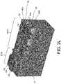
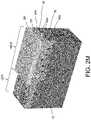
- FIGS. 2A-2Oare perspective views showing the steps in forming the memory cells of the present invention.
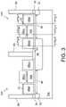
- FIG. 3is a side cross sectional view of a pair of memory cells.
- FIG. 4is a side cross sectional view of a memory cell in the memory cell area of the semiconductor substrate taken along the line FIG. 4 - FIG. 4 in FIG. 3 .
- FIG. 5is a side cross sectional view of a memory cell in the memory cell area of the semiconductor substrate taken along the line FIG. 5 - FIG. 5 in FIG. 3 .
- FIG. 6is a side cross sectional view of a memory cell in the memory cell area of the semiconductor substrate taken along the line FIG. 6 - FIG. 6 in FIG. 3 .
- FIGS. 7-8are side cross sectional views of a logic device in the logic device area of the semiconductor substrate.
- FIG. 9is a side cross sectional view of floating gates and control gates, and fin-to-fin spacing for two adjacent fin pairs FP n .
- FIGS. 10A-10Care perspective views showing the steps in forming the memory cells according to an alternate embodiment of the present invention.
- FIG. 11is a plan view of the layout of the memory cells according to the alternative embodiment of the present invention.
- the present inventionconfigures the memory cell array to actually enhance such capacitive coupling between some, but not all, adjacent floating gates, which can be used as a fine tuning mechanism when programming the memory cells.
- FIGS. 2A-2Othere are shown perspective cross-sectional views of steps in the process of making FinFET memory cells in a memory cell area (MCA) of a semiconductor substrate (also referred to as substrate) 10 of a memory device.
- the memory devicecan include just the memory cell array, or can include additional components such as supporting circuitry and logic devices.
- Logic devicesif included, are advantageously concurrently formed in a logic device area (LDA) of the substrate 10 .
- LDAlogic device area
- the processbegins by forming a layer of silicon dioxide 12 (also referred to as oxide) on the upper surface 11 of the semiconductor substrate 10 , where semiconductor substrate 10 may be formed of P type single crystalline silicon.
- Oxide layer 12can be formed by deposition or by thermal oxidation.
- a photolithography masking processis then used to pattern the oxide layer 12 (i.e. selectively remove some portions of the layer but not others).
- the photolithography masking processincludes coating photoresist material 13 on the oxide layer 12 , which is followed by exposing and developing the photoresist to remove the photoresist material from the memory cell area MCA while maintaining the photoresist in the logic device area LDA.
- An oxide etchis then used to remove the exposed portions of oxide layer 12 from the memory cell area MCA leaving the substrate 10 exposed (the photoresist 13 protects oxide layer 12 from the etch in the logic device area LDA).
- a silicon etchis used to recess the exposed upper surface 11 of the substrate 10 in the memory cell area MCA.
- Oxide layer 12 and the photoresist 13protect the logic device area LDA from this silicon etch.
- the resulting structureis shown in FIG. 2A , where the upper surface 11 of the substrate 10 in the memory cell area MCA is recessed below the upper surface 11 of the substrate 10 in the logic device area LDA by a recess amount R.
- an oxide layer 14is formed on the structure.
- a silicon nitride (“nitride”) layer 16is formed on oxide layer 14 .
- An insulation layer 18(e.g., amorphous carbon) is formed on nitride layer 16 .
- the insulation layer 18is patterned by forming photoresist 19 , selectively removing strips of the photoresist 19 in the memory cell area MCA and logic device area LDA, and removing the underlying exposed portions of the insulation layer 18 to form trenches 20 in the insulation layer 18 that extend down to and expose the underlying nitride layer 16 , as shown in FIG. 2B .
- oxide spacersare then formed in the trenches 20 . Formation of spacers is well known in the art, and involves the deposition of a material over the contour of a structure, followed by an anisotropic etch process, whereby the material is removed from horizontal surfaces of the structure, while the material remains largely intact on vertically oriented surfaces of the structure (often with a rounded upper surface). In the present case, oxide spacers are formed along the sidewalls of trenches 20 .
- Portions of the oxide spacers in trenches 20can be removed by covering the structure with photoresist followed by partial photoresist removal so that portions of the oxide spacers are exposed and can removed by oxide etch (e.g., portions of the spacers in the logic device area LDA).
- oxide etche.g., portions of the spacers in the logic device area LDA.
- a nitride etchis then used to remove the exposed portions of nitride layer 16 (i.e., all but the portions of nitride layer 16 underneath the remaining oxide spacers), followed by an oxide etch to remove exposed portions of oxide layer 14 and the remaining oxide spacers.
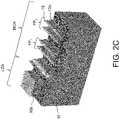
- a silicon etchis then used to recess the exposed surface portions of the substrate 10 , forming fins 10 a of the substrate 10 in the memory cell area MCA and fins 10 b (also referred to herein as logic fins 10 b ) of the silicon substrate in the logic device area LDA, as shown in FIG. 2C .
- fins 10 aare parallel to each other, and arranged in pairs (fin pairs FP n ). Two fin pairs FP 1 and FP 2 are shown in FIG. 2C , although one skilled in the art would understand there are many of such fin pairs FP n formed in the memory cell area MCA.
- each fin pair FP nthe two fins 10 a thereof are separated from each other by a distance D 1 .
- Each fin pair FP nis separated from an adjacent fin pair FP n by a distance D 2 , where distance D 2 is greater than distance D 1 .
- the structureis covered in a thick layer of oxide (i.e., STI oxide) 24 , which is then planarized (e.g., by chemical mechanical polish—CMP).
- a nitride layer 26is formed over planarized oxide layer 24 .
- Photoresistis formed over nitride layer 26 , and removed from the memory cell area MCA. Etches are used to remove the exposed nitride layers 26 / 16 and oxide layer 14 in the memory cell area MCA, and recess thick oxide layer 24 to below the tops of fins 10 a in the memory cell area MCA, as shown in FIG. 2D (after photoresist removal).
- a floating gate oxide layer 28is formed on the structure.
- a floating gate polysilicon (“poly”) layeris formed on the oxide layer 28 by a first polysilicon deposition.
- a chemical mechanical polishis used to planarize the poly layer, using the oxide layer 28 as a stop layer, which removes poly layer from the logic device area LDA.
- a poly etch backis used to recess poly layer in the memory cell area MCA.
- the poly layeris then patterned (photoresist formation, exposure, and partial removal, followed by poly etch), so that strips 30 of the poly layer remain, each extending along the top and sidewalls of one of the fins 10 a in the memory cell area MCA, as shown in FIG. 2E (after photoresist removal).
- An insulation layer 32(e.g., ONO, which includes oxide, nitride, oxide sublayers) is formed over the structure.
- a buffer oxide layer 34is formed on the structure, followed by an oxide etch back, which fills the spaces between the fins 10 a with the buffer oxide layer 34 .
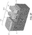
- Photoresist 35is formed over the structure, and partially removed, leaving strips of photoresist 35 covering the fin pairs FP n , but leaving the areas between adjacent fin pairs FP n exposed.
- An oxide etchis then used to remove the exposed portion of buffer oxide layer 34 between the fin pairs FP n (i.e., remove the exposed portion of buffer oxide layer 34 between poly strips 30 ), as shown in FIG. 2F .
- the buffer oxide layer 34is maintained between the two poly strips 30 of the fin pair FP n .
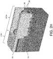
- Photoresist 37is formed over the structure, and partially removed, leaving strips of photoresist 37 extending across the fin pairs FP n (i.e., strips of photoresist 37 extend lengthwise orthogonally to the length of fin pairs FP n ). Etches are performed to remove exposed portions of poly layer, insulation layer 32 , and poly strips 30 between the strips of photoresist 37 , as shown in FIG. 2G .
- Strips 36 of the poly layerremain, each extending down between fin pairs FP n , but not extending down between the fins 10 a of each fin pair FP n (i.e., oxide 34 prevents poly strips 36 from extending down between the fins 10 a of each fin pair FP n ).
- Distinct poly blocks 30 a(remaining portions of poly strips 30 ) remain, where each poly block 30 a is disposed underneath one of the poly strips 36 .
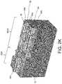
- Oxide spacers 38are then formed by oxide deposition and anisotropic etch, to cover the exposed sidewalls of poly strips 36 and poly blocks 30 a .
- Photoresist 39is formed over the structure, and partially removed to expose portions of the memory cell area MCA (i.e., the area between adjacent poly strips 36 ), as shown in FIG. 2H .
- An implantation processis performed to form source regions 40 (best seen in FIG. 3 ) in the fins 10 a between the adjacent poly strips 36 .
- An isotropic oxide etchis used to remove oxide spacers 38 on the exposed sidewalls of poly strips 36 and poly blocks 30 a (i.e., those sidewalls facing each other for adjacent poly strips 36 ).
- a layer of oxide (tunnel oxide) 42is formed on the exposed sidewalls of poly blocks 30 a (e.g., by high temperature oxidation—HTO).
- HTOhigh temperature oxidation
- Photoresistis formed over the structure, and partially removed to expose portions of the memory cell area MCA (i.e., for adjacent poly blocks 30 a on the same fin 10 a , the area around sidewalls facing away from each other are exposed, leaving oxide spacers 38 exposed).
- An implantation processis performed to implant material into the portions of fins 10 a adjacent oxide spacers 38 on sidewalls of poly blocks 30 a . These implanted areas of fins 10 a will eventually be disposed underneath the word line gates which are formed later.
- An oxide etchis then used to remove oxide from, and to leave exposed, top and side surface portions of the fins 10 a that were just implanted. After photoresist removal, an oxide layer 44 (word line oxide) is formed on the exposed top and side surfaces of fins 10 a .
- FIG. 2Iexcept source region 40 , which is better shown in FIG. 3 ).
- Photoresistis formed over the structure, and removed from the logic device area LDA.
- a series of etchesare performed to remove the oxide and nitride layers down to the thick oxide layer 24 , and to recess thick oxide layer 24 , so that fins 10 b protrude and are partially exposed in the logic device area LDA.
- An oxide layer(not shown) is then formed to cover the exposed top and side surfaces of fins 10 b in the logic device area LDA.
- a poly layer 46is then formed over the structure by a third poly deposition.
- the poly layer 46is planarized by CMP (using oxide on poly strips 36 in the memory cell area MCA as a CMP stop layer), as shown in FIG. 2J .
- Photoresistis formed on the structure and removed from the memory cell area MCA.
- An isotropic poly etchis used to recess the poly layer 46 in the memory cell area MCA.
- photoresistis formed over the structure, and selectively removed leaving strips of photoresist extending across the fins 10 a / 10 b in both the memory cell area MCA and logic device area LDA.
- a poly etchis used to remove exposed portions of poly layer 46 (except for those portions under the strips of photoresist).
- an insulation layer 48preferably formed of a low K material—i.e., one with a dielectric constant below that of oxide—such as SiON) is formed over the structure. The resulting structure is shown in FIG. 2K .
- strips 46 a / 46 b of poly layer 46remain, each extending across the fins 10 a and laterally adjacent to poly blocks 30 a (see FIG. 2G ) and poly strips 36 (i.e., poly blocks 30 a and poly strips 36 are between poly strips 46 a and 46 b ).
- poly strips 46 c of poly layer 46remain (disposed under the portion of layer 48 indicated by the arrow in FIG. 2K ), each extending across fins 10 b (only one set of fins 10 b and one strip 46 c are shown for simplicity).
- An etchis performed, leaving spacers of the insulation layer 48 on the vertical surfaces of the structure.
- An isotropic etchis used to expose fins 10 b adjacent poly strip 46 c in the logic device area LDA.
- a hard mask layer 50(e.g., SiCN) is formed over the structure. Photoresist is formed on the structure and patterned to selectively expose portions of the hard mask layer 50 between adjacent poly strips 46 a and between adjacent poly strips 46 b in the memory cell area MCA, and portions of the hard mask layer 50 adjacent poly strip 46 c in the logic device area LDA. Etches are used to remove the exposed portions of hard mask layer 50 and oxide layer 44 in the memory cell area MCA, exposing portions of fins 10 a between adjacent poly strips 46 a and between adjacent poly strips 46 b .
- Epitaxial layer 54expands the size of source/drain regions (for easier contact formation and reliability) and increases carrier mobility in the fins 10 a / 10 b for better conduction.
- the resulting structureis shown in FIG. 2L (except for source/drain regions 40 / 52 which are better shown in FIG. 3 , and source/drain regions 40 L/ 52 L which are better shown in FIG. 7 ).
- hard mask layer 50is then removed by etch.
- the structureis then covered by a layer of nitride 56 .
- a thick layer of oxide 58is formed over the structure, and planarized by CMP.
- Photoresist 59is formed over the structure, and selectively removed from the logic device area LDA.
- An oxide etchis used to expose poly strips 46 c .
- a poly etchis then used to remove poly strips 46 c from logic device area LDA, as shown in FIG. 2 M.
- An oxide etchis used to remove the oxide on the fins 10 b which was previously under poly strips 46 c , leaving portions of the fins 10 b in logic device area LDA exposed.
- An oxide layer 60is then formed which covers the exposed fins 10 b in logic device area LDA.
- a layer of high K material 62(i.e. having a dielectric constant K greater than that of oxide, such as HfO2, ZrO2, TiO2, Ta2O5, or other adequate materials) is formed on the structure (namely on oxide layer 60 ).
- One or more metal layersare then formed on the structure. For example, a TiN layer 64 is formed on the structure, followed by a thick layer of tungsten 66 , followed by CMP using the high K layer 62 in the logic device area LDA as the stop layer (which removes the TiN layer 64 and tungsten 66 on the structure except for strips thereof where poly strips 46 c were located).
- the resulting structureis shown in FIG. 2N (except for oxide layer 60 and high K material layer 62 which are better shown in FIGS. 7 and 8 ), where strips of TiN layer 64 and tungsten 66 in the logic device area LDA extend across fins 10 b (effectively replacing dummy poly strip 46 c which was previously removed).
- a nitride layer 68is formed over the structure, and an oxide layer 70 is formed on nitride layer 68 .
- Photoresistis formed over the structure, and patterned so as to expose portions of oxide layer 70 over poly strips 46 b in memory cell area MCA. Etches are performed to remove portions of oxide layer 70 , nitride layer 68 and thick oxide layer 58 over, and expose the tops of, poly strips 46 b .
- salicide 72is formed on the top surface of poly strips 46 b by Ti/Pt deposition and anneal. Any excessive Ti is removed by Ti etch, if required. Oxide is deposited to fill in the area over salicide 72 .
- Photoresistis formed over the structure, and patterned to remove portions of the photoresist vertically over source/drain regions 40 / 52 in the memory cell area MCA, and vertically over the source/drain regions 40 L/ 52 L in the logic device area LDA. Contact holes are then formed where the photoresist was removed by a series of etches that extend down to and expose respective source or drain regions. Specifically, contact holes in the memory cell area MCA each extend down to and expose one of the drain regions 52 , contact holes in the memory cell area MCA extend down to and expose the source regions 40 , contact holes in the logic device area LDA extend down to and expose the source regions 40 L, and contact holes in the logic device area LDA extend down to and expose the drain regions 52 L.
- TiNis deposited on the structure, and a layer of tungsten is deposited on the TiN layer.
- a CMPis used to remove the TiN and tungsten layers, except for in the contact holes.
- the TiN and tungsten in the contact holesform contacts, namely, drain contacts 88 that extend down to, and make electrical contact with, drain regions 52 , source contacts 90 that extend down to, and make electrical contact with, source regions 40 , source contacts 92 that extend down to, and make electrical contact with, source regions 40 L, and drain contacts 94 that extend down to, and make electrical contact with, drain regions 52 L.
- the final structureis shown in FIG. 2O . Further contact processing may be performed to further extend and route the respective source and drain contacts 88 / 90 / 92 / 94 , as well as form other contacts for poly strips 46 a / 46 b as needed.
- FIG. 3shows a pair of the memory cells 100 formed on one of the fins 10 a in the memory cell area MCA, although it should be appreciated that additional pairs of memory cells are formed end to end on each fin 10 a .
- Each of the fins 10 a(as well as fins 10 b in the logic device area LDA) includes a pair of opposing side surfaces 10 c and 10 d that extend upwardly and terminate in a top surface 10 e (see FIG. 4 ).
- Each memory cell 100includes a source region 40 and a drain region 52 , which define a channel region 96 of the semiconductor substrate there between.
- the channel region 96extends along the side surfaces 10 c / 10 d and top surface 10 e of the fin 10 a between the source and drain regions 40 / 52 .
- Poly block 30 ais a floating gate which wraps around and is insulated from the side surfaces 10 c / 10 d and top surface 10 e (i.e., the floating gate 30 a extends along and is insulated from the side surfaces 10 c / 10 d and top surface 10 e of fin 10 a ), for controlling the conductivity of a first portion of the channel region 96 , as best shown in FIG. 4 .
- a word line gate 46 w 1is that portion of poly strip 46 b that wraps around and is insulated from the side surfaces 10 c / 10 d and top surface 10 e of the fin 10 a (i.e., the word line gate 46 w 1 extends along and is insulated from the side surfaces 10 c / 10 d and top surface 10 e of fin 10 a ), for controlling the conductivity of a second portion of the channel region 96 , as best shown in FIG. 5 .
- Silicide 72 on word line gate 46 w 1increases conductivity.
- An erase gate 46 egis that portion of poly strip 46 a which wraps around and is insulated from the source region 40 of the fin 10 a (i.e., the erase gate 46 eg extends along and is insulated from the side surfaces 10 c / 10 d and top surface 10 e of fin 10 a ), as best shown in FIG. 6 .
- a control gate 36 cgis that portion of poly strip 36 (i.e., a first continuous strip of conductive material) that is disposed over and insulated from the floating gate 30 a . Drain contacts 88 and source contact 90 (extending down and making contact with respective epitaxial layer portions 54 ) are further shown in FIG. 3 .
- FIG. 7shows a logic device 102 , formed on one of the logic fins 10 b in logic device area LDA, which includes a logic source region 40 L and a logic drain region 52 L that define a logic channel region 98 of the semiconductor substrate there between.
- the logic channel region 98extends along the side surfaces 10 c / 10 d and top surface 10 e of the fin 10 b (best shown in FIG. 8 ) between the logic source and logic drain regions 40 L/ 52 L.
- a logic gate 104is (collectively) those portions of TiN layer 64 and tungsten layer 66 that wrap around the side surfaces 10 c / 10 d and top surface 10 e of the logic fin 10 b (and insulated therefrom by oxide layer 60 and high K material layer 62 ) for controlling the conductivity of the logic channel region 98 , as best shown in FIG. 8 .
- multiple logic devices 102are operated in parallel. Specifically, as shown in FIGS.
- the logic gates 104 for the eight logic devicesare formed as a continuous strip of conductive material (i.e., a second continuous strip of conductive material), namely, the TiN layer 64 layer and the tungsten layer 66 , a single source contact 92 (extending down and making contact with respective epitaxial layer portions 54 ) connects to the eight logic source regions 40 L of the eight logic devices 102 , and a single drain contact 94 (extending down and making contact with respective epitaxial layer portions 54 ) connects to the eight logic drain regions 52 L of the eight logic devices 102 ).
- the logic gates 104 for the eight logic devicesare formed as a continuous strip of conductive material (i.e., a second continuous strip of conductive material), namely, the TiN layer 64 layer and the tungsten layer 66 , a single source contact 92 (extending down and making contact with respective epitaxial layer portions 54 ) connects to the eight logic source regions 40 L of the eight logic devices 102 , and a single drain contact 94 (extending down and making
- the eight logic devicesare operated simultaneously in parallel, to provide eight times the operating current that would be supplied by a single logic device 102 formed on only a single logic fin 10 b .
- the number of logic devices 102 operated together in parallelcan be any number (two or greater), and/or individual logic devices 102 can be operated separately and individually, depending upon the operating current needed from the logic device(s).
- the total number of logic devices 102 on one of the logic fins 10 b , the total number of logic fins 10 b , and the total number of logic devices 102 in the logic device area LDAcan vary.
- Reference to “logic” fin, “logic” source region, “logic” drain region, “logic” channel regionwithout limitation, merely means these elements are in the logic device area LDA and are different from like elements in the memory cell area MCA.
- FIG. 9shows the fin spacing and control gate configuration for the memory cells in the memory cell area MCA.
- Fins 10 aare parallel to each other (i.e., each have a length that is parallel to a first direction such as the column direction).
- the two fins 10 aare adjacent to each other (i.e., no intervening fins therebetween), and are spaced from each other by a distance D 1 .
- the spacing of the fins from one fin pair FP n to an adjacent fin pair FP nis a distance D 2 , which is greater than distance D 1 .
- FIG. 9shows the fin spacing and control gate configuration for the memory cells in the memory cell area MCA.
- Fins 10 aare parallel to each other (i.e., each have a length that is parallel to a first direction such as the column direction).
- the two fins 10 aare adjacent to each other (i.e., no intervening fins therebetween), and are spaced from each other by a distance D 1 .
- FIG. 9illustrates first and second fins 10 a (from left to right) of Fin pair FP 1 separated by a distance D 1 (i.e., a first distance), and third and fourth fins 10 a (from left to right) of fin pair FP 2 separated by a distance D 1 (i.e., a second distance), where the first and second distances are equal to each other.
- the second and third finsare separated by a distance D 2 (i.e., a third distance) which is greater than the first and second distances D 1 .
- the poly strip 36has a portion 36 a that extends down and is disposed between the floating gates 30 a of two adjacent fin pairs FP n , but no such portion extends down or is disposed between fins 10 a of the same fin pair FP n .
- This configurationresults in enhancing capacitive coupling between the two floating gates 30 a of the same fin pair FP n because of closer proximity and no portion of the poly strip 36 is disposed therebetween, while minimizing capacitive coupling between floating gates 30 a of different but adjacent fin pairs FP n because of lesser proximity and portion 36 a of poly strip 36 is disposed therebetween.
- Capacitive coupling between floating gates with the same fin pair FP ncan be used for fine tuning programming.
- the control gate 36 cgcan be used to implement the majority of the programming operation.
- capacitive coupling from the right hand floating gate 30 a of fin pair FP 1i.e., in the tuning memory cell 100 t
- capacitive coupling from the right hand floating gate 30 a of fin pair FP 1can then be used to fine tune the programming of the left hand floating gate 30 a of fin pair FP 1 (programmed memory cell 100 p ), while not disturbing the programing state or operation of the floating gates 30 a in fin pair FP 2 .
- tuning accuracyis critical when using memory cells to store weights for artificial neural networks. Precision better than single elementary charge is difficult or not possible for weight tuning using traditional memory programming/erase methods. Scaling of memory cell geometry in advanced technology nodes greatly reduces the tuning accuracy due to increased effect of each elementary charge.
- Capacitive couplingis not limited to a single elementary charge of the weighted charge storage element (namely the floating gate).
- Capacitive coupling from an adjacent memory cell (i.e., the tuning memory cell 100 t ) to the memory cell being programmed (i.e., the programmed memory cell 100 p )need not result in a discrete potential change on the programmed memory cell.
- capacitive coupling from an adjacent floating gate to fine tune the programming of the programmed memory cellprovides for a much finer resolution in memory cell program tuning.
- An elementary charge transferred or removed from the adjacent tuning memory cellwill change the programming value of the programmed memory cell proportional to the capacitive coupling between the two memory cells.
- the change to the programmed memory cellwill be much less than that of an elementary charge. Therefore, the resolution, and thus the final accuracy, of program tuning may be adjusted to a desired level with process adjustments to the floating gate voltage coupling and/or the rate of charge transfer to the adjacent tuning memory cell.
- FIGS. 10A-10C and 11illustrate an alternate embodiment, where the memory cell source regions are formed as a continuous source line along a fin extending in the row direction.
- the processbegins with the same structure as shown in FIG. 2B , except that an additional trench is formed that is orthogonal to, and extends across, trenches 20 .
- an additional source fin 10 fis formed that extends orthogonal to fins 10 a in the memory cell area MCA, as illustrated in FIG. 10A .
- FIG. 10Bshows the resulting structure in FIG. 10B , where source fin 10 f crosses fins 10 in an orthogonal manner.
- FIG. 10Cthe resulting structure is shown in FIG. 10C , where subsequently formed elements such as poly strips 30 are formed in a similar manner but traversing over source fin 10 f .
- the remaining steps described above with respect to FIGS. 2F-2Oare performed to complete the formation of the memory cells 100 and logic devices 102 .
- the final layout of the memory cells 100 in this alternate embodimentis shown in FIG. 11 , and is the same as layout of the memory cells 100 in the embodiment of FIGS. 2A-2O , except a continuous source line 40 a extends along source fin 10 f , where the source region 40 for each memory cell is formed in fin 10 a at an intersection of fin 10 a and source fin 10 f.
- the alternate embodimentis advantageous because the continuous source line 40 a extends across the isolation regions between adjacent cells (in the row direction), allowing for scaling the cells down to a smaller size because this configuration avoids the need to form source line contacts for each pair of memory cells.
- the continuous source line 40 a extending along the source fin 10 fcan be electrically connected to a strap through periodic strap contacts (e.g., every 32 or 64 columns). By having a contact every 32 or 64 columns instead of one for every column, the size of the memory cells and thus a memory array of the memory cells can be significantly reduced.
- adjacentincludes “directly adjacent” (no intermediate materials, elements or space disposed there between) and “indirectly adjacent” (intermediate materials, elements or space disposed there between)
- mounted toincludes “directly mounted to” (no intermediate materials, elements or space disposed there between) and “indirectly mounted to” (intermediate materials, elements or spaced disposed there between)
- electrically coupledincludes “directly electrically coupled to” (no intermediate materials or elements there between that electrically connect the elements together) and “indirectly electrically coupled to” (intermediate materials or elements there between that electrically connect the elements together).
- forming an element “over a substrate”can include forming the element directly on the substrate with no intermediate materials/elements there between, as well as forming the element indirectly on the substrate with one or more intermediate materials/elements there between.
Landscapes
- Non-Volatile Memory (AREA)
- Semiconductor Memories (AREA)
- Insulated Gate Type Field-Effect Transistor (AREA)
- Metal-Oxide And Bipolar Metal-Oxide Semiconductor Integrated Circuits (AREA)
Abstract
Description
Claims (18)
Priority Applications (7)
| Application Number | Priority Date | Filing Date | Title |
|---|---|---|---|
| US17/069,563US11362100B2 (en) | 2020-03-24 | 2020-10-13 | FinFET split gate non-volatile memory cells with enhanced floating gate to floating gate capacitive coupling |
| EP20803701.0AEP4128352B1 (en) | 2020-03-24 | 2020-10-14 | Finfet split gate non-volatile memory cells with enhanced floating gate to floating gate capacitive coupling |
| PCT/US2020/055606WO2021194552A1 (en) | 2020-03-24 | 2020-10-14 | Finfet split gate non-volatile memory cells with enhanced floating gate to floating gate capacitive coupling |
| JP2022556564AJP7256930B2 (en) | 2020-03-24 | 2020-10-14 | FinFET split-gate nonvolatile memory cell with enhanced floating-gate capacitive coupling |
| KR1020227031887AKR102487233B1 (en) | 2020-03-24 | 2020-10-14 | FINFET Split Gate Non-Volatile Memory Cell with Enhanced Floating Gate to Floating Gate Capacitive Coupling |
| CN202080098756.8ACN115335996B (en) | 2020-03-24 | 2020-10-14 | FINFET split-gate nonvolatile memory cells with enhanced floating-gate-to-floating-gate capacitive coupling |
| TW110109895ATWI757123B (en) | 2020-03-24 | 2021-03-19 | Finfet split gate non-volatile memory cells with enhanced floating gate to floating gate capacitive coupling |
Applications Claiming Priority (2)
| Application Number | Priority Date | Filing Date | Title |
|---|---|---|---|
| US202062994187P | 2020-03-24 | 2020-03-24 | |
| US17/069,563US11362100B2 (en) | 2020-03-24 | 2020-10-13 | FinFET split gate non-volatile memory cells with enhanced floating gate to floating gate capacitive coupling |
Publications (2)
| Publication Number | Publication Date |
|---|---|
| US20210305264A1 US20210305264A1 (en) | 2021-09-30 |
| US11362100B2true US11362100B2 (en) | 2022-06-14 |
Family
ID=77856427
Family Applications (1)
| Application Number | Title | Priority Date | Filing Date |
|---|---|---|---|
| US17/069,563Active2041-01-13US11362100B2 (en) | 2020-03-24 | 2020-10-13 | FinFET split gate non-volatile memory cells with enhanced floating gate to floating gate capacitive coupling |
Country Status (7)
| Country | Link |
|---|---|
| US (1) | US11362100B2 (en) |
| EP (1) | EP4128352B1 (en) |
| JP (1) | JP7256930B2 (en) |
| KR (1) | KR102487233B1 (en) |
| CN (1) | CN115335996B (en) |
| TW (1) | TWI757123B (en) |
| WO (1) | WO2021194552A1 (en) |
Families Citing this family (3)
| Publication number | Priority date | Publication date | Assignee | Title |
|---|---|---|---|---|
| US11362100B2 (en)* | 2020-03-24 | 2022-06-14 | Silicon Storage Technology, Inc. | FinFET split gate non-volatile memory cells with enhanced floating gate to floating gate capacitive coupling |
| CN115084155A (en) | 2021-03-11 | 2022-09-20 | 联华电子股份有限公司 | Silicon-oxygen-nitrogen-oxygen-silicon memory cell for fin field effect transistor and forming method |
| CN117915663B (en)* | 2024-03-20 | 2024-06-18 | 合肥晶合集成电路股份有限公司 | Flash memory and method for making the same |
Citations (58)
| Publication number | Priority date | Publication date | Assignee | Title |
|---|---|---|---|---|
| US5029130A (en) | 1990-01-22 | 1991-07-02 | Silicon Storage Technology, Inc. | Single transistor non-valatile electrically alterable semiconductor memory device |
| US6747310B2 (en) | 2002-10-07 | 2004-06-08 | Actrans System Inc. | Flash memory cells with separated self-aligned select and erase gates, and process of fabrication |
| US20050012137A1 (en) | 2003-07-18 | 2005-01-20 | Amitay Levi | Nonvolatile memory cell having floating gate, control gate and separate erase gate, an array of such memory cells, and method of manufacturing |
| US20050023591A1 (en)* | 2003-07-30 | 2005-02-03 | Yi Ding | Nonvolatile memory cell with multiple floating gates formed after the select gate and having upward protrusions |
| US20050227435A1 (en) | 2004-04-12 | 2005-10-13 | Samsung Electronics Co., Ltd. | Non-volatile memory devices and method for forming the same |
| US20050266638A1 (en) | 2004-05-31 | 2005-12-01 | Cho Eun-Suk | Methods of forming non-volatile memory cells including fin structures and related devices |
| US20050280000A1 (en) | 2004-06-22 | 2005-12-22 | Renesas Technology Corp. | Semiconductor memory device |
| US20060097310A1 (en) | 2004-11-08 | 2006-05-11 | Samsung Electronics Co., Ltd. | Non-volatile memory devices including divided charge storage structures and methods of fabricating the same |
| US20060208307A1 (en) | 2005-03-21 | 2006-09-21 | Ko-Hsing Chang | Split gate flash memory and manufacturing method thereof |
| US20060249779A1 (en) | 2005-05-06 | 2006-11-09 | Samsung Electronics Co., Ltd. | Multi-bit multi-level non-volatile memory device and methods of operating and fabricating the same |
| US20060278915A1 (en)* | 2005-06-09 | 2006-12-14 | Di-Hong Lee | FinFET split gate EEPROM structure and method of its fabrication |
| US20070090443A1 (en)* | 2005-10-26 | 2007-04-26 | Samsung Electronics Co., Ltd. | Method of fabricating a semiconductor device having self-aligned floating gate and related device |
| EP1801857A2 (en) | 2005-12-20 | 2007-06-27 | Samsung Electronics Co., Ltd. | Multi-bit non-volatile memory devices and methods of fabricating the same |
| US20070158730A1 (en) | 2006-01-10 | 2007-07-12 | Burnett James D | Integrated circuit using FinFETs and having a static random access memory (SRAM) |
| US7315056B2 (en) | 2004-06-07 | 2008-01-01 | Silicon Storage Technology, Inc. | Semiconductor memory array of floating gate memory cells with program/erase and select gates |
| EP1939942A2 (en) | 2006-12-27 | 2008-07-02 | Samsung Electronics Co., Ltd. | Semiconductor device and method of fabricating the same |
| KR20080061764A (en) | 2006-12-28 | 2008-07-03 | 삼성전자주식회사 | Nonvolatile Memory Device and Manufacturing Method Thereof |
| US20080173921A1 (en) | 2007-01-24 | 2008-07-24 | Freescale Semiconductor, Inc. | Electronic device including trenches and discontinuous storage elements and processes of forming and using the same |
| US7410913B2 (en) | 2005-09-23 | 2008-08-12 | Samsung Electronics Co., Ltd. | Method of manufacturing silicon rich oxide (SRO) and semiconductor device employing SRO |
| US7423310B2 (en) | 2004-09-29 | 2008-09-09 | Infineon Technologies Ag | Charge-trapping memory cell and charge-trapping memory device |
| US20090090955A1 (en) | 2007-10-03 | 2009-04-09 | Nanya Technology Corporation | Elevated channel flash device and manufacturing method thereof |
| US7847338B2 (en)* | 2007-10-24 | 2010-12-07 | Yuniarto Widjaja | Semiconductor memory having both volatile and non-volatile functionality and method of operating |
| US20100320525A1 (en) | 2009-06-18 | 2010-12-23 | Satoshi Nagashima | Nonvolatile semiconductor memory device and method of manufacturing nonvolatile semiconductor memory device |
| US7868375B2 (en) | 2007-08-06 | 2011-01-11 | Silicon Storage Technology, Inc. | Split gate non-volatile flash memory cell having a floating gate, control gate, select gate and an erase gate with an overhang over the floating gate, array and method of manufacturing |
| US8068370B2 (en) | 2008-04-18 | 2011-11-29 | Macronix International Co., Ltd. | Floating gate memory device with interpoly charge trapping structure |
| US8148768B2 (en) | 2008-11-26 | 2012-04-03 | Silicon Storage Technology, Inc. | Non-volatile memory cell with self aligned floating and erase gates, and method of making same |
| US8420476B2 (en) | 2010-05-27 | 2013-04-16 | International Business Machines Corporation | Integrated circuit with finFETs and MIM fin capacitor |
| US8461640B2 (en) | 2009-09-08 | 2013-06-11 | Silicon Storage Technology, Inc. | FIN-FET non-volatile memory cell, and an array and method of manufacturing |
| US20130270627A1 (en) | 2012-04-11 | 2013-10-17 | International Business Machines Corporation | FinFET NON-VOLATILE MEMORY AND METHOD OF FABRICATION |
| US8710485B2 (en) | 2011-04-28 | 2014-04-29 | Kabushiki Kaisha Toshiba | Semiconductor device and method of manufacturing the same |
| US8941153B2 (en) | 2009-11-20 | 2015-01-27 | Taiwan Semiconductor Manufacturing Company, Ltd. | FinFETs with different fin heights |
| US20150035039A1 (en)* | 2013-07-31 | 2015-02-05 | Qualcomm Incorporated | Logic finfet high-k/conductive gate embedded multiple time programmable flash memory |
| TW201539454A (en) | 2013-12-05 | 2015-10-16 | Conversant Intellectual Property Man Inc | Three-dimensional non-volatile memory with charge storage node isolation |
| US20160020219A1 (en) | 2014-07-16 | 2016-01-21 | Taiwan Semiconductor Manufacturing Co., Ltd. | Recess technique to embed flash memory in soi technology |
| US9276006B1 (en) | 2015-01-05 | 2016-03-01 | Silicon Storage Technology, Inc. | Split gate non-volatile flash memory cell having metal-enhanced gates and method of making same |
| US9276005B1 (en) | 2014-12-04 | 2016-03-01 | Silicon Storage Technology, Inc. | Non-volatile memory array with concurrently formed low and high voltage logic devices |
| US20160064398A1 (en) | 2014-09-02 | 2016-03-03 | Globalfoundries Singapore Pte. Ltd. | Integrated circuits with finfet nonvolatile memory |
| US20160218110A1 (en) | 2015-01-23 | 2016-07-28 | Silicon Storage Technology, Inc. | Method Of Forming Self-Aligned Split-Gate Memory Cell Array With Metal Gates And Logic Devices |
| US20160307911A1 (en)* | 2015-04-16 | 2016-10-20 | Taiwan Semiconductor Manufacturing Co., Ltd. | Method for Preventing Floating Gate Variation |
| US20160379987A1 (en) | 2015-06-25 | 2016-12-29 | Taiwan Semiconductor Manufacturing Co., Ltd. | Structure with emedded efs3 and finfet device |
| US9614048B2 (en) | 2014-06-17 | 2017-04-04 | Taiwan Semiconductor Manufacturing Co., Ltd. | Split gate flash memory structure and method of making the split gate flash memory structure |
| US9634018B2 (en) | 2015-03-17 | 2017-04-25 | Silicon Storage Technology, Inc. | Split gate non-volatile memory cell with 3D finFET structure, and method of making same |
| US20170117285A1 (en) | 2015-10-21 | 2017-04-27 | Silicon Storage Technology, Inc. | Method Of Forming Flash Memory With Separate Wordline And Erase Gates |
| US20170125429A1 (en)* | 2015-11-03 | 2017-05-04 | Silicon Storage Technology, Inc. | Split Gate Non-volatile Flash Memory Cell Having Metal Gates And Method Of Making Same |
| US20170243955A1 (en) | 2016-02-24 | 2017-08-24 | Renesas Electronics Corporation | Method for manufacturing semiconductor device |
| US20170271484A1 (en) | 2016-03-21 | 2017-09-21 | Globalfoundries Inc. | Finfet based flash memory cell |
| US20170301683A1 (en) | 2016-04-19 | 2017-10-19 | United Microelectronics Corp. | Semiconductor device with split gate flash memory cell structure and method of manufacturing the same |
| US20170345840A1 (en)* | 2016-05-24 | 2017-11-30 | Silicon Storage Technology, Inc. | Method Of Integrating FINFET CMOS Devices With Embedded Nonvolatile Memory Cells |
| US20180315765A1 (en) | 2017-04-27 | 2018-11-01 | Taiwan Semiconductor Manufacturing Co., Ltd. | Integrated Circuit and Manufacturing Method Thereof |
| US10217850B2 (en) | 2016-04-20 | 2019-02-26 | Silicon Storage Technology, Inc. | Method of forming pairs of three-gate non-volatile flash memory cells using two polysilicon deposition steps |
| US10312247B1 (en)* | 2018-03-22 | 2019-06-04 | Silicon Storage Technology, Inc. | Two transistor FinFET-based split gate non-volatile floating gate flash memory and method of fabrication |
| US10468428B1 (en) | 2018-04-19 | 2019-11-05 | Silicon Storage Technology, Inc. | Split gate non-volatile memory cells and logic devices with FinFET structure, and method of making same |
| US10644012B2 (en) | 2018-07-05 | 2020-05-05 | Silicon Storage Technology, Inc. | Method of making split gate non-volatile memory cells with three-dimensional FinFET structure, and method of making same |
| US20200176459A1 (en) | 2018-12-03 | 2020-06-04 | Silicon Storage Technology, Inc. | Split Gate Non-volatile Memory Cells With FINFET Structure And HKMG Memory And Logic Gates, And Method Of Making Same |
| US20200176578A1 (en)* | 2018-12-03 | 2020-06-04 | Silicon Storage Technology, Inc. | FINFET-Based Split Gate Non-volatile Flash Memory With Extended Source Line FINFET, and Method Of Fabrication |
| US20210193671A1 (en)* | 2019-12-20 | 2021-06-24 | Silicon Storage Technology, Inc. | Method Of Forming A Device With Split Gate Non-volatile Memory Cells, HV Devices Having Planar Channel Regions And FINFET Logic Devices |
| US11114451B1 (en)* | 2020-02-27 | 2021-09-07 | Silicon Storage Technology, Inc. | Method of forming a device with FinFET split gate non-volatile memory cells and FinFET logic devices |
| WO2021194552A1 (en)* | 2020-03-24 | 2021-09-30 | Silicon Storage Technology, Inc. | Finfet split gate non-volatile memory cells with enhanced floating gate to floating gate capacitive coupling |
Family Cites Families (2)
| Publication number | Priority date | Publication date | Assignee | Title |
|---|---|---|---|---|
| CN102074582B (en)* | 2009-11-20 | 2013-06-12 | 台湾积体电路制造股份有限公司 | Integrated circuit structure and method of forming the same |
| US10332884B2 (en)* | 2017-11-02 | 2019-06-25 | United Microelectronics Corp. | FinFET semiconductor device |
- 2020
- 2020-10-13USUS17/069,563patent/US11362100B2/enactiveActive
- 2020-10-14JPJP2022556564Apatent/JP7256930B2/enactiveActive
- 2020-10-14WOPCT/US2020/055606patent/WO2021194552A1/ennot_activeCeased
- 2020-10-14EPEP20803701.0Apatent/EP4128352B1/enactiveActive
- 2020-10-14CNCN202080098756.8Apatent/CN115335996B/enactiveActive
- 2020-10-14KRKR1020227031887Apatent/KR102487233B1/enactiveActive
- 2021
- 2021-03-19TWTW110109895Apatent/TWI757123B/enactive
Patent Citations (69)
| Publication number | Priority date | Publication date | Assignee | Title |
|---|---|---|---|---|
| US5029130A (en) | 1990-01-22 | 1991-07-02 | Silicon Storage Technology, Inc. | Single transistor non-valatile electrically alterable semiconductor memory device |
| US6747310B2 (en) | 2002-10-07 | 2004-06-08 | Actrans System Inc. | Flash memory cells with separated self-aligned select and erase gates, and process of fabrication |
| US20050012137A1 (en) | 2003-07-18 | 2005-01-20 | Amitay Levi | Nonvolatile memory cell having floating gate, control gate and separate erase gate, an array of such memory cells, and method of manufacturing |
| US20050023591A1 (en)* | 2003-07-30 | 2005-02-03 | Yi Ding | Nonvolatile memory cell with multiple floating gates formed after the select gate and having upward protrusions |
| US20050227435A1 (en) | 2004-04-12 | 2005-10-13 | Samsung Electronics Co., Ltd. | Non-volatile memory devices and method for forming the same |
| US20050266638A1 (en) | 2004-05-31 | 2005-12-01 | Cho Eun-Suk | Methods of forming non-volatile memory cells including fin structures and related devices |
| US7315056B2 (en) | 2004-06-07 | 2008-01-01 | Silicon Storage Technology, Inc. | Semiconductor memory array of floating gate memory cells with program/erase and select gates |
| US20050280000A1 (en) | 2004-06-22 | 2005-12-22 | Renesas Technology Corp. | Semiconductor memory device |
| US7423310B2 (en) | 2004-09-29 | 2008-09-09 | Infineon Technologies Ag | Charge-trapping memory cell and charge-trapping memory device |
| US20060097310A1 (en) | 2004-11-08 | 2006-05-11 | Samsung Electronics Co., Ltd. | Non-volatile memory devices including divided charge storage structures and methods of fabricating the same |
| US20060208307A1 (en) | 2005-03-21 | 2006-09-21 | Ko-Hsing Chang | Split gate flash memory and manufacturing method thereof |
| US20060249779A1 (en) | 2005-05-06 | 2006-11-09 | Samsung Electronics Co., Ltd. | Multi-bit multi-level non-volatile memory device and methods of operating and fabricating the same |
| US20060278915A1 (en)* | 2005-06-09 | 2006-12-14 | Di-Hong Lee | FinFET split gate EEPROM structure and method of its fabrication |
| US7410913B2 (en) | 2005-09-23 | 2008-08-12 | Samsung Electronics Co., Ltd. | Method of manufacturing silicon rich oxide (SRO) and semiconductor device employing SRO |
| US20070090443A1 (en)* | 2005-10-26 | 2007-04-26 | Samsung Electronics Co., Ltd. | Method of fabricating a semiconductor device having self-aligned floating gate and related device |
| US7329580B2 (en)* | 2005-10-26 | 2008-02-12 | Samsung Electronics Co., Ltd. | Method of fabricating a semiconductor device having self-aligned floating gate and related device |
| EP1801857A2 (en) | 2005-12-20 | 2007-06-27 | Samsung Electronics Co., Ltd. | Multi-bit non-volatile memory devices and methods of fabricating the same |
| US20070158730A1 (en) | 2006-01-10 | 2007-07-12 | Burnett James D | Integrated circuit using FinFETs and having a static random access memory (SRAM) |
| EP1939942A2 (en) | 2006-12-27 | 2008-07-02 | Samsung Electronics Co., Ltd. | Semiconductor device and method of fabricating the same |
| KR20080061764A (en) | 2006-12-28 | 2008-07-03 | 삼성전자주식회사 | Nonvolatile Memory Device and Manufacturing Method Thereof |
| US20080173921A1 (en) | 2007-01-24 | 2008-07-24 | Freescale Semiconductor, Inc. | Electronic device including trenches and discontinuous storage elements and processes of forming and using the same |
| US7868375B2 (en) | 2007-08-06 | 2011-01-11 | Silicon Storage Technology, Inc. | Split gate non-volatile flash memory cell having a floating gate, control gate, select gate and an erase gate with an overhang over the floating gate, array and method of manufacturing |
| US7927994B1 (en) | 2007-08-06 | 2011-04-19 | Silicon Storage Technology, Inc. | Split gate non-volatile flash memory cell having a floating gate, control gate, select gate and an erase gate with an overhang over the floating gate, array and method of manufacturing |
| US20090090955A1 (en) | 2007-10-03 | 2009-04-09 | Nanya Technology Corporation | Elevated channel flash device and manufacturing method thereof |
| US7847338B2 (en)* | 2007-10-24 | 2010-12-07 | Yuniarto Widjaja | Semiconductor memory having both volatile and non-volatile functionality and method of operating |
| US8068370B2 (en) | 2008-04-18 | 2011-11-29 | Macronix International Co., Ltd. | Floating gate memory device with interpoly charge trapping structure |
| US8148768B2 (en) | 2008-11-26 | 2012-04-03 | Silicon Storage Technology, Inc. | Non-volatile memory cell with self aligned floating and erase gates, and method of making same |
| US20100320525A1 (en) | 2009-06-18 | 2010-12-23 | Satoshi Nagashima | Nonvolatile semiconductor memory device and method of manufacturing nonvolatile semiconductor memory device |
| US8461640B2 (en) | 2009-09-08 | 2013-06-11 | Silicon Storage Technology, Inc. | FIN-FET non-volatile memory cell, and an array and method of manufacturing |
| US8941153B2 (en) | 2009-11-20 | 2015-01-27 | Taiwan Semiconductor Manufacturing Company, Ltd. | FinFETs with different fin heights |
| US8420476B2 (en) | 2010-05-27 | 2013-04-16 | International Business Machines Corporation | Integrated circuit with finFETs and MIM fin capacitor |
| US8710485B2 (en) | 2011-04-28 | 2014-04-29 | Kabushiki Kaisha Toshiba | Semiconductor device and method of manufacturing the same |
| US20130270627A1 (en) | 2012-04-11 | 2013-10-17 | International Business Machines Corporation | FinFET NON-VOLATILE MEMORY AND METHOD OF FABRICATION |
| US20150035039A1 (en)* | 2013-07-31 | 2015-02-05 | Qualcomm Incorporated | Logic finfet high-k/conductive gate embedded multiple time programmable flash memory |
| US9406689B2 (en) | 2013-07-31 | 2016-08-02 | Qualcomm Incorporated | Logic finFET high-K/conductive gate embedded multiple time programmable flash memory |
| TW201539454A (en) | 2013-12-05 | 2015-10-16 | Conversant Intellectual Property Man Inc | Three-dimensional non-volatile memory with charge storage node isolation |
| US9614048B2 (en) | 2014-06-17 | 2017-04-04 | Taiwan Semiconductor Manufacturing Co., Ltd. | Split gate flash memory structure and method of making the split gate flash memory structure |
| US20160020219A1 (en) | 2014-07-16 | 2016-01-21 | Taiwan Semiconductor Manufacturing Co., Ltd. | Recess technique to embed flash memory in soi technology |
| US20160064398A1 (en) | 2014-09-02 | 2016-03-03 | Globalfoundries Singapore Pte. Ltd. | Integrated circuits with finfet nonvolatile memory |
| US9276005B1 (en) | 2014-12-04 | 2016-03-01 | Silicon Storage Technology, Inc. | Non-volatile memory array with concurrently formed low and high voltage logic devices |
| US9276006B1 (en) | 2015-01-05 | 2016-03-01 | Silicon Storage Technology, Inc. | Split gate non-volatile flash memory cell having metal-enhanced gates and method of making same |
| US20160218110A1 (en) | 2015-01-23 | 2016-07-28 | Silicon Storage Technology, Inc. | Method Of Forming Self-Aligned Split-Gate Memory Cell Array With Metal Gates And Logic Devices |
| US9634018B2 (en) | 2015-03-17 | 2017-04-25 | Silicon Storage Technology, Inc. | Split gate non-volatile memory cell with 3D finFET structure, and method of making same |
| US20160307911A1 (en)* | 2015-04-16 | 2016-10-20 | Taiwan Semiconductor Manufacturing Co., Ltd. | Method for Preventing Floating Gate Variation |
| US20160379987A1 (en) | 2015-06-25 | 2016-12-29 | Taiwan Semiconductor Manufacturing Co., Ltd. | Structure with emedded efs3 and finfet device |
| US20170117285A1 (en) | 2015-10-21 | 2017-04-27 | Silicon Storage Technology, Inc. | Method Of Forming Flash Memory With Separate Wordline And Erase Gates |
| US20170125429A1 (en)* | 2015-11-03 | 2017-05-04 | Silicon Storage Technology, Inc. | Split Gate Non-volatile Flash Memory Cell Having Metal Gates And Method Of Making Same |
| US10249631B2 (en) | 2015-11-03 | 2019-04-02 | Silicon Storage Technology, Inc. | Split gate non-volatile flash memory cell having metal gates |
| US9972630B2 (en) | 2015-11-03 | 2018-05-15 | Silicon Storage Technology, Inc. | Split gate non-volatile flash memory cell having metal gates and method of making same |
| US20180226420A1 (en)* | 2015-11-03 | 2018-08-09 | Sillicon Storage Technology, Inc. | Split Gate Non-volatile Flash Memory Cell Having Metal Gates |
| US20170243955A1 (en) | 2016-02-24 | 2017-08-24 | Renesas Electronics Corporation | Method for manufacturing semiconductor device |
| US20170271484A1 (en) | 2016-03-21 | 2017-09-21 | Globalfoundries Inc. | Finfet based flash memory cell |
| US20170301683A1 (en) | 2016-04-19 | 2017-10-19 | United Microelectronics Corp. | Semiconductor device with split gate flash memory cell structure and method of manufacturing the same |
| US10217850B2 (en) | 2016-04-20 | 2019-02-26 | Silicon Storage Technology, Inc. | Method of forming pairs of three-gate non-volatile flash memory cells using two polysilicon deposition steps |
| US9985042B2 (en) | 2016-05-24 | 2018-05-29 | Silicon Storage Technology, Inc. | Method of integrating FinFET CMOS devices with embedded nonvolatile memory cells |
| US20170345840A1 (en)* | 2016-05-24 | 2017-11-30 | Silicon Storage Technology, Inc. | Method Of Integrating FINFET CMOS Devices With Embedded Nonvolatile Memory Cells |
| US20180315765A1 (en) | 2017-04-27 | 2018-11-01 | Taiwan Semiconductor Manufacturing Co., Ltd. | Integrated Circuit and Manufacturing Method Thereof |
| US10312247B1 (en)* | 2018-03-22 | 2019-06-04 | Silicon Storage Technology, Inc. | Two transistor FinFET-based split gate non-volatile floating gate flash memory and method of fabrication |
| US10468428B1 (en) | 2018-04-19 | 2019-11-05 | Silicon Storage Technology, Inc. | Split gate non-volatile memory cells and logic devices with FinFET structure, and method of making same |
| US10644012B2 (en) | 2018-07-05 | 2020-05-05 | Silicon Storage Technology, Inc. | Method of making split gate non-volatile memory cells with three-dimensional FinFET structure, and method of making same |
| US10727240B2 (en) | 2018-07-05 | 2020-07-28 | Silicon Store Technology, Inc. | Split gate non-volatile memory cells with three-dimensional FinFET structure |
| US20200176578A1 (en)* | 2018-12-03 | 2020-06-04 | Silicon Storage Technology, Inc. | FINFET-Based Split Gate Non-volatile Flash Memory With Extended Source Line FINFET, and Method Of Fabrication |
| US20200176459A1 (en) | 2018-12-03 | 2020-06-04 | Silicon Storage Technology, Inc. | Split Gate Non-volatile Memory Cells With FINFET Structure And HKMG Memory And Logic Gates, And Method Of Making Same |
| US10797142B2 (en) | 2018-12-03 | 2020-10-06 | Silicon Storage Technology, Inc. | FinFET-based split gate non-volatile flash memory with extended source line FinFET, and method of fabrication |
| US10937794B2 (en)* | 2018-12-03 | 2021-03-02 | Silicon Storage Technology, Inc. | Split gate non-volatile memory cells with FinFET structure and HKMG memory and logic gates, and method of making same |
| US20210193671A1 (en)* | 2019-12-20 | 2021-06-24 | Silicon Storage Technology, Inc. | Method Of Forming A Device With Split Gate Non-volatile Memory Cells, HV Devices Having Planar Channel Regions And FINFET Logic Devices |
| US11114451B1 (en)* | 2020-02-27 | 2021-09-07 | Silicon Storage Technology, Inc. | Method of forming a device with FinFET split gate non-volatile memory cells and FinFET logic devices |
| WO2021194552A1 (en)* | 2020-03-24 | 2021-09-30 | Silicon Storage Technology, Inc. | Finfet split gate non-volatile memory cells with enhanced floating gate to floating gate capacitive coupling |
| US20210305264A1 (en)* | 2020-03-24 | 2021-09-30 | Silicon Storage Technology, Inc. | Finfet split gate non-volatile memory cells with enhanced floating gate to floating gate capacitive coupling |
Non-Patent Citations (4)
| Title |
|---|
| Eun Suk Cho, et al., "Hf-silicate Inter-poly Dielectric Technology for Sub 70 nm Body Tied FinFET Flash Memory," VLSI Technology, Digest of Technical Papers, 2005 Symposium on Kyoto, Japan, Jun. 14-16, 2005, Piscataway, NJ, USA, IEEE, Piscataway, NJ, USA, Jun. 14, 2005, pp. 208-209, XPO10818301. |
| U.S. Appl. No. 16/724,010, filed Dec. 20, 2019 entitled "Method of Forming a Device with Split Gate Non-volatile Memory Cells, HV Devices Having Planar Channel Regions and FINFET Logic Devices," Jourba et al. |
| U.S. Appl. No. 16/803,876, filed Feb. 27, 2020, entitled "Method of Forming a Device with FINFET Split Gate Non-volatile Memory Cells and FINFET Logic Devices," Zhou, et al. |
| Written Opinion in PCT/US2020/055606 (Year: 2020).* |
Also Published As
| Publication number | Publication date |
|---|---|
| EP4128352A1 (en) | 2023-02-08 |
| EP4128352B1 (en) | 2024-01-17 |
| TWI757123B (en) | 2022-03-01 |
| JP2023510028A (en) | 2023-03-10 |
| JP7256930B2 (en) | 2023-04-12 |
| KR102487233B1 (en) | 2023-01-10 |
| WO2021194552A1 (en) | 2021-09-30 |
| KR20220130261A (en) | 2022-09-26 |
| US20210305264A1 (en) | 2021-09-30 |
| CN115335996B (en) | 2023-07-25 |
| TW202141754A (en) | 2021-11-01 |
| CN115335996A (en) | 2022-11-11 |
Similar Documents
| Publication | Publication Date | Title |
|---|---|---|
| CN111868928B (en) | Split-gate nonvolatile floating gate flash memory based on dual-transistor fin field effect transistor and method for manufacturing the same | |
| US11362100B2 (en) | FinFET split gate non-volatile memory cells with enhanced floating gate to floating gate capacitive coupling | |
| US11594453B2 (en) | Method of forming a device with split gate non-volatile memory cells, HV devices having planar channel regions and FINFET logic devices | |
| US7723775B2 (en) | NAND flash memory device having a contact for controlling a well potential | |
| KR102380362B1 (en) | FinFET-based Removable Gate Non-Volatile Flash Memory with Scalable Source Line FinFET, and Manufacturing Method | |
| TWI748847B (en) | Method of forming a device with finfet split gate non-volatile memory cells and finfet logic devices | |
| US20230189520A1 (en) | Split gate non-volatile memory cells, hv and logic devices with finfet structures, and method of making same | |
| US20230290864A1 (en) | Method of forming a device with planar split gate non-volatile memory cells, planar hv devices, and finfet logic devices on a substrate |
Legal Events
| Date | Code | Title | Description |
|---|---|---|---|
| AS | Assignment | Owner name:SILICON STORAGE TECHNOLOGY, INC., CALIFORNIA Free format text:ASSIGNMENT OF ASSIGNORS INTEREST;ASSIGNORS:ZHOU, FENG;LIU, XIAN;LEMKE, STEVEN;AND OTHERS;REEL/FRAME:054043/0728 Effective date:20201008 | |
| FEPP | Fee payment procedure | Free format text:ENTITY STATUS SET TO UNDISCOUNTED (ORIGINAL EVENT CODE: BIG.); ENTITY STATUS OF PATENT OWNER: LARGE ENTITY | |
| AS | Assignment | Owner name:WELLS FARGO BANK, NATIONAL ASSOCIATION, AS COLLATERAL AGENT, MINNESOTA Free format text:SECURITY INTEREST;ASSIGNORS:MICROCHIP TECHNOLOGY INCORPORATED;SILICON STORAGE TECHNOLOGY, INC.;ATMEL CORPORATION;AND OTHERS;REEL/FRAME:055671/0612 Effective date:20201217 | |
| AS | Assignment | Owner name:WELLS FARGO BANK, NATIONAL ASSOCIATION, AS NOTES COLLATERAL AGENT, MINNESOTA Free format text:SECURITY INTEREST;ASSIGNORS:MICROCHIP TECHNOLOGY INCORPORATED;SILICON STORAGE TECHNOLOGY, INC.;ATMEL CORPORATION;AND OTHERS;REEL/FRAME:057935/0474 Effective date:20210528 | |
| STPP | Information on status: patent application and granting procedure in general | Free format text:DOCKETED NEW CASE - READY FOR EXAMINATION | |
| AS | Assignment | Owner name:WELLS FARGO BANK, NATIONAL ASSOCIATION, AS NOTES COLLATERAL AGENT, MINNESOTA Free format text:GRANT OF SECURITY INTEREST IN PATENT RIGHTS;ASSIGNORS:MICROCHIP TECHNOLOGY INCORPORATED;SILICON STORAGE TECHNOLOGY, INC.;ATMEL CORPORATION;AND OTHERS;REEL/FRAME:058214/0625 Effective date:20211117 Owner name:JPMORGAN CHASE BANK, N.A., AS ADMINISTRATIVE AGENT, ILLINOIS Free format text:GRANT OF SECURITY INTEREST IN PATENT RIGHTS;ASSIGNORS:MICROCHIP TECHNOLOGY INCORPORATED;SILICON STORAGE TECHNOLOGY, INC.;ATMEL CORPORATION;AND OTHERS;REEL/FRAME:058214/0380 Effective date:20211117 Owner name:WELLS FARGO BANK, NATIONAL ASSOCIATION, AS NOTES COLLATERAL AGENT, MINNESOTA Free format text:GRANT OF SECURITY INTEREST IN PATENT RIGHTS;ASSIGNORS:MICROCHIP TECHNOLOGY INCORPORATED;SILICON STORAGE TECHNOLOGY, INC.;ATMEL CORPORATION;AND OTHERS;REEL/FRAME:058214/0238 Effective date:20211117 | |
| AS | Assignment | Owner name:MICROSEMI STORAGE SOLUTIONS, INC., ARIZONA Free format text:RELEASE BY SECURED PARTY;ASSIGNOR:JPMORGAN CHASE BANK, N.A., AS ADMINISTRATIVE AGENT;REEL/FRAME:059264/0384 Effective date:20220218 Owner name:MICROSEMI CORPORATION, ARIZONA Free format text:RELEASE BY SECURED PARTY;ASSIGNOR:JPMORGAN CHASE BANK, N.A., AS ADMINISTRATIVE AGENT;REEL/FRAME:059264/0384 Effective date:20220218 Owner name:ATMEL CORPORATION, ARIZONA Free format text:RELEASE BY SECURED PARTY;ASSIGNOR:JPMORGAN CHASE BANK, N.A., AS ADMINISTRATIVE AGENT;REEL/FRAME:059264/0384 Effective date:20220218 Owner name:SILICON STORAGE TECHNOLOGY, INC., ARIZONA Free format text:RELEASE BY SECURED PARTY;ASSIGNOR:JPMORGAN CHASE BANK, N.A., AS ADMINISTRATIVE AGENT;REEL/FRAME:059264/0384 Effective date:20220218 Owner name:MICROCHIP TECHNOLOGY INCORPORATED, ARIZONA Free format text:RELEASE BY SECURED PARTY;ASSIGNOR:JPMORGAN CHASE BANK, N.A., AS ADMINISTRATIVE AGENT;REEL/FRAME:059264/0384 Effective date:20220218 | |
| AS | Assignment | Owner name:MICROSEMI STORAGE SOLUTIONS, INC., ARIZONA Free format text:RELEASE BY SECURED PARTY;ASSIGNOR:WELLS FARGO BANK, NATIONAL ASSOCIATION, AS NOTES COLLATERAL AGENT;REEL/FRAME:059357/0823 Effective date:20220228 Owner name:MICROSEMI CORPORATION, ARIZONA Free format text:RELEASE BY SECURED PARTY;ASSIGNOR:WELLS FARGO BANK, NATIONAL ASSOCIATION, AS NOTES COLLATERAL AGENT;REEL/FRAME:059357/0823 Effective date:20220228 Owner name:ATMEL CORPORATION, ARIZONA Free format text:RELEASE BY SECURED PARTY;ASSIGNOR:WELLS FARGO BANK, NATIONAL ASSOCIATION, AS NOTES COLLATERAL AGENT;REEL/FRAME:059357/0823 Effective date:20220228 Owner name:SILICON STORAGE TECHNOLOGY, INC., ARIZONA Free format text:RELEASE BY SECURED PARTY;ASSIGNOR:WELLS FARGO BANK, NATIONAL ASSOCIATION, AS NOTES COLLATERAL AGENT;REEL/FRAME:059357/0823 Effective date:20220228 Owner name:MICROCHIP TECHNOLOGY INCORPORATED, ARIZONA Free format text:RELEASE BY SECURED PARTY;ASSIGNOR:WELLS FARGO BANK, NATIONAL ASSOCIATION, AS NOTES COLLATERAL AGENT;REEL/FRAME:059357/0823 Effective date:20220228 Owner name:MICROSEMI STORAGE SOLUTIONS, INC., ARIZONA Free format text:RELEASE BY SECURED PARTY;ASSIGNOR:WELLS FARGO BANK, NATIONAL ASSOCIATION, AS NOTES COLLATERAL AGENT;REEL/FRAME:059358/0335 Effective date:20220228 Owner name:MICROSEMI CORPORATION, ARIZONA Free format text:RELEASE BY SECURED PARTY;ASSIGNOR:WELLS FARGO BANK, NATIONAL ASSOCIATION, AS NOTES COLLATERAL AGENT;REEL/FRAME:059358/0335 Effective date:20220228 Owner name:ATMEL CORPORATION, ARIZONA Free format text:RELEASE BY SECURED PARTY;ASSIGNOR:WELLS FARGO BANK, NATIONAL ASSOCIATION, AS NOTES COLLATERAL AGENT;REEL/FRAME:059358/0335 Effective date:20220228 Owner name:SILICON STORAGE TECHNOLOGY, INC., ARIZONA Free format text:RELEASE BY SECURED PARTY;ASSIGNOR:WELLS FARGO BANK, NATIONAL ASSOCIATION, AS NOTES COLLATERAL AGENT;REEL/FRAME:059358/0335 Effective date:20220228 Owner name:MICROCHIP TECHNOLOGY INCORPORATED, ARIZONA Free format text:RELEASE BY SECURED PARTY;ASSIGNOR:WELLS FARGO BANK, NATIONAL ASSOCIATION, AS NOTES COLLATERAL AGENT;REEL/FRAME:059358/0335 Effective date:20220228 | |
| AS | Assignment | Owner name:MICROSEMI STORAGE SOLUTIONS, INC., ARIZONA Free format text:RELEASE BY SECURED PARTY;ASSIGNOR:WELLS FARGO BANK, NATIONAL ASSOCIATION, AS NOTES COLLATERAL AGENT;REEL/FRAME:059863/0400 Effective date:20220228 Owner name:MICROSEMI CORPORATION, ARIZONA Free format text:RELEASE BY SECURED PARTY;ASSIGNOR:WELLS FARGO BANK, NATIONAL ASSOCIATION, AS NOTES COLLATERAL AGENT;REEL/FRAME:059863/0400 Effective date:20220228 Owner name:ATMEL CORPORATION, ARIZONA Free format text:RELEASE BY SECURED PARTY;ASSIGNOR:WELLS FARGO BANK, NATIONAL ASSOCIATION, AS NOTES COLLATERAL AGENT;REEL/FRAME:059863/0400 Effective date:20220228 Owner name:SILICON STORAGE TECHNOLOGY, INC., ARIZONA Free format text:RELEASE BY SECURED PARTY;ASSIGNOR:WELLS FARGO BANK, NATIONAL ASSOCIATION, AS NOTES COLLATERAL AGENT;REEL/FRAME:059863/0400 Effective date:20220228 Owner name:MICROCHIP TECHNOLOGY INCORPORATED, ARIZONA Free format text:RELEASE BY SECURED PARTY;ASSIGNOR:WELLS FARGO BANK, NATIONAL ASSOCIATION, AS NOTES COLLATERAL AGENT;REEL/FRAME:059863/0400 Effective date:20220228 | |
| AS | Assignment | Owner name:MICROSEMI STORAGE SOLUTIONS, INC., ARIZONA Free format text:RELEASE BY SECURED PARTY;ASSIGNOR:WELLS FARGO BANK, NATIONAL ASSOCIATION, AS NOTES COLLATERAL AGENT;REEL/FRAME:059363/0001 Effective date:20220228 Owner name:MICROSEMI CORPORATION, ARIZONA Free format text:RELEASE BY SECURED PARTY;ASSIGNOR:WELLS FARGO BANK, NATIONAL ASSOCIATION, AS NOTES COLLATERAL AGENT;REEL/FRAME:059363/0001 Effective date:20220228 Owner name:ATMEL CORPORATION, ARIZONA Free format text:RELEASE BY SECURED PARTY;ASSIGNOR:WELLS FARGO BANK, NATIONAL ASSOCIATION, AS NOTES COLLATERAL AGENT;REEL/FRAME:059363/0001 Effective date:20220228 Owner name:SILICON STORAGE TECHNOLOGY, INC., ARIZONA Free format text:RELEASE BY SECURED PARTY;ASSIGNOR:WELLS FARGO BANK, NATIONAL ASSOCIATION, AS NOTES COLLATERAL AGENT;REEL/FRAME:059363/0001 Effective date:20220228 Owner name:MICROCHIP TECHNOLOGY INCORPORATED, ARIZONA Free format text:RELEASE BY SECURED PARTY;ASSIGNOR:WELLS FARGO BANK, NATIONAL ASSOCIATION, AS NOTES COLLATERAL AGENT;REEL/FRAME:059363/0001 Effective date:20220228 | |
| STPP | Information on status: patent application and granting procedure in general | Free format text:NON FINAL ACTION MAILED | |
| STPP | Information on status: patent application and granting procedure in general | Free format text:RESPONSE TO NON-FINAL OFFICE ACTION ENTERED AND FORWARDED TO EXAMINER | |
| STPP | Information on status: patent application and granting procedure in general | Free format text:NOTICE OF ALLOWANCE MAILED -- APPLICATION RECEIVED IN OFFICE OF PUBLICATIONS | |
| STPP | Information on status: patent application and granting procedure in general | Free format text:PUBLICATIONS -- ISSUE FEE PAYMENT VERIFIED | |
| STCF | Information on status: patent grant | Free format text:PATENTED CASE |