US11361794B2 - Apparatus and method for storing wave signals in a cavity - Google Patents
Apparatus and method for storing wave signals in a cavityDownload PDFInfo
- Publication number
- US11361794B2 US11361794B2US16/529,479US201916529479AUS11361794B2US 11361794 B2US11361794 B2US 11361794B2US 201916529479 AUS201916529479 AUS 201916529479AUS 11361794 B2US11361794 B2US 11361794B2
- Authority
- US
- United States
- Prior art keywords
- electromagnetic wave
- cavity
- wave signal
- signal
- transmitters
- Prior art date
- Legal status (The legal status is an assumption and is not a legal conclusion. Google has not performed a legal analysis and makes no representation as to the accuracy of the status listed.)
- Active, expires
Links
Images


Classifications
- G—PHYSICS
- G02—OPTICS
- G02B—OPTICAL ELEMENTS, SYSTEMS OR APPARATUS
- G02B5/00—Optical elements other than lenses
- G02B5/08—Mirrors
- G02B5/0816—Multilayer mirrors, i.e. having two or more reflecting layers
- G—PHYSICS
- G02—OPTICS
- G02B—OPTICAL ELEMENTS, SYSTEMS OR APPARATUS
- G02B5/00—Optical elements other than lenses
- G02B5/08—Mirrors
- G—PHYSICS
- G11—INFORMATION STORAGE
- G11B—INFORMATION STORAGE BASED ON RELATIVE MOVEMENT BETWEEN RECORD CARRIER AND TRANSDUCER
- G11B7/00—Recording or reproducing by optical means, e.g. recording using a thermal beam of optical radiation by modifying optical properties or the physical structure, reproducing using an optical beam at lower power by sensing optical properties; Record carriers therefor
- G11B7/004—Recording, reproducing or erasing methods; Read, write or erase circuits therefor
- G11B7/0045—Recording
- G—PHYSICS
- G02—OPTICS
- G02B—OPTICAL ELEMENTS, SYSTEMS OR APPARATUS
- G02B5/00—Optical elements other than lenses
- G02B5/08—Mirrors
- G02B5/09—Multifaceted or polygonal mirrors, e.g. polygonal scanning mirrors; Fresnel mirrors
- G—PHYSICS
- G11—INFORMATION STORAGE
- G11C—STATIC STORES
- G11C13/00—Digital stores characterised by the use of storage elements not covered by groups G11C11/00, G11C23/00, or G11C25/00
- G11C13/04—Digital stores characterised by the use of storage elements not covered by groups G11C11/00, G11C23/00, or G11C25/00 using optical elements ; using other beam accessed elements, e.g. electron or ion beam
- G11C13/042—Digital stores characterised by the use of storage elements not covered by groups G11C11/00, G11C23/00, or G11C25/00 using optical elements ; using other beam accessed elements, e.g. electron or ion beam using information stored in the form of interference pattern
Definitions
- SSDssolid state drives
- HDDshard disk drives
- SSDssolid state drives
- Conventional data centers based on those solid state-based storage deviceshave a variety of drawbacks.
- data storage using those conventional storage devicesconsumes a large amount of power and requires expensive maintenance.
- data storage involving many of those conventional storage devicesgenerates a large amount of heat, necessitating cooling systems, which in turn require additional cost and energy consumption.
- the throughput at which data can be read from or written to those conventional electromagnetic wave storage devicesis limited by the speed of electronics to, for example, a few Gb/s.
- the present inventionrelates to an apparatus comprising a cavity comprising interior surfaces or reflecting elements, one or more transmitters configured to receive an electrical signal, transform the electrical signal into an electromagnetic wave signal and introduce the electromagnetic wave signal into an inside of the cavity, and one or more receivers configured to retrieve the electromagnetic wave signal, transform the electromagnetic wave signal to a corresponding electrical signal and transmit the corresponding electrical signal to the outside of the cavity, wherein the electromagnetic wave signal is contained within the inside of the cavity by undergoing a series of reflections or traversals between the interior surfaces or the reflecting elements of or within the cavity.
- the apparatusfurther comprises one or more regenerators configured to re-amplify, re-shape, and/or re-time the electromagnetic wave signal traveling within the inside of the cavity.
- the regeneratorsmay include an all-optical regenerator or an optoelectronic regenerator.
- the inside of the cavityis configured to enable an atmospheric pressure level that is different than the atmospheric pressure level at the outside of the cavity. In at least one embodiment, the inside of the cavity is configured to enable an atmospheric pressure level that is lower than the atmospheric pressure level at the outside of the cavity.
- the electromagnetic wave signalcomprises a modulated laser beam.
- the electromagnetic wave signalcomprises any beam shape. In at least one embodiment, the electromagnetic wave signal comprises a Gaussian beam. In at least one embodiment, the electromagnetic wave signal comprises a non-Gaussian beam.
- the electromagnetic wave signalcomprises a spatial mode. In at least one embodiment, the electromagnetic wave signal comprises an orbital angular momentum (OAM) mode.
- OAMorbital angular momentum
- the cavityis substantially sealed.
- the cavitycomprises a cubic cavity, a rectangular-shaped cavity, a tube cavity, a torus-shaped cavity, a spherical cavity, a polyhedron cavity, a parallelogram-shaped cavity, prism-shaped cavity, or an egg-shaped cavity.
- the cavitycomprises a resonating cavity configured to create resonance at one or more frequencies of the electromagnetic wave signal.
- the one or more transmitterscomprise at least one laser and at least one modulator.
- the one or more transmitterscomprise at least one directly modulated laser.
- At least one of the one or more transmitters and at least one of the one or more receiversare placed together in a transceiver.
- the interior surfaces of the cavityare made at least in part of mirrors, reflecting coatings, gratings, or photonic microstructure materials configured to reflect or regenerate or separate or process the incident electromagnetic wave signal.
- the one or more regeneratorscomprise at least one amplifier and at least one absorber.
- the one or more regeneratorscomprise at least one amplifier configured to operate in a saturation regime.
- the one or more regeneratorscomprise a nonlinear filter.
- the reflecting elementsfurther comprise a plurality of second parallel plates positioned perpendicular to the first parallel plates and a plurality of third parallel plates positioned perpendicular to the first and second parallel plates such that the first, second and third parallel plates define a plurality of sub-cavities within the inside of the cavity, wherein at least a portion of each side of each one of the second and third parallel plates comprises a reflective surface or a surface with a reflective element disposed thereon and the electromagnetic wave signal is contained within an inside of at least one of the sub-cavities until retrieved.
- the second parallel platesare positioned substantially equidistant from each other.
- the third parallel platesare positioned substantially equidistant from each other.
- the methodfurther comprises refocusing or reshaping, by using at least one of lenses, gratings, optical materials, and metamaterials, the electromagnetic wave signal traveling within the inside of the cavity.
- the electromagnetic wave storage devicefurther comprises a signal focusing device, which is placed on, or adjacent to, one or more of the interior surfaces or reflecting elements of the cavity and configured to separate two adjacent overlapping electromagnetic wave beams and focus them to separate points on the reflective interior surfaces or reflecting elements, and the method further comprises the steps of focusing, by using the signal focusing device, the incident electromagnetic wave signal, and redirecting, by using the signal focusing device, the electromagnetic wave signal to an opposite direction.
- a signal focusing devicewhich is placed on, or adjacent to, one or more of the interior surfaces or reflecting elements of the cavity and configured to separate two adjacent overlapping electromagnetic wave beams and focus them to separate points on the reflective interior surfaces or reflecting elements
- the methodfurther comprises the steps of focusing, by using the signal focusing device, the incident electromagnetic wave signal, and redirecting, by using the signal focusing device, the electromagnetic wave signal to an opposite direction.
- the signal focusing devicecomprises a gradient index material, a photonic crystal structure, a mirror structure, or a diffraction structure.
- the cavitycomprises a cubic cavity and portions of the interior surfaces for two opposing faces of the cubic cavity comprise mirrors, and the method further comprises reflecting, by the mirrors, the incident electromagnetic wave signal such that the electromagnetic wave signal travels in a zig-zag manner within a first plane substantially perpendicular to the two opposing faces of the cubic cavity.
- the electromagnetic wave storage devicefurther comprises a signal directing element
- the methodfurther comprises directing, by the signal directing element, the electromagnetic wave signal to travel within a second plane, which is substantially parallel and adjacent to the first plane.
- the electromagnetic wave storage devicefurther comprises a signal directing element
- the methodfurther comprises directing, by the signal directing element, the electromagnetic wave signal to travel within a second plane, which is substantially perpendicular to the first plane.
- the one or more regeneratorscomprise an all-optical regenerator and the step of re-amplifying, re-shaping, and/or re-timing the electromagnetic wave signal is performed by the all-optical regenerator in an optical domain.
- FIG. 3is a schematic diagram of a regenerator and its operation in accordance with an exemplary embodiment of the present invention.
- FIG. 4Ais a cross-sectional view of interior surfaces of two opposing sides of the cubic cavity of FIG. 1 , illustrating an electromagnetic wave beam traversing between the interior surfaces in accordance with an exemplary embodiment of the present invention.
- FIG. 4Cis a cross-sectional view of interior surfaces of two opposing sides of the cubic cavity of FIG. 1 , illustrating an electromagnetic wave beam traversing between the interior surfaces in accordance with an exemplary embodiment of the present invention.
- FIG. 5illustrates the Rayleigh range of a collimated electromagnetic wave beam.
- Information or any kind of datacan be stored as electromagnetic waves (e.g., lasers, optical beam, radio frequency (RF) signals, other types of electromagnetic wave signals, to name a few), which can be transmitted and/or reflected between structures or within structures in various transmission media (e.g., free space, vacuum, crystals, nonlinear media, optical waveguides, optical fibers, to name a few).
- electromagnetic wavese.g., lasers, optical beam, radio frequency (RF) signals, other types of electromagnetic wave signals, to name a few
- RFradio frequency
- a recirculating loopmay be used to store “data in motion” by keeping electromagnetic wave signals carrying data in a continuous motion, transmitted and/or reflected between or within structures and regenerated (e.g., by signal amplification or regeneration) as needed.
- the recirculating loopmay be formed by, for example, satellites or other vessels that reflect or otherwise retransmit the data in free space or through a waveguide, such as one or more pieces of optical fiber.
- the recirculating loopmay also comprise a waveguide, such as an optical fiber.
- the enclosed space within a cavitymay be filled with a material (e.g., solid, crystal, amorphous material, liquid, etc.) having an index of refraction greater than one, where electromagnetic wave signals travel more slowly than in vacuum.
- a cavitymay be a solid material (e.g., crystal, amorphous solid, to name a few) enclosed by its own interior and exterior surfaces.
- such a material filling the cavityis configured to allow storage or containment of electromagnetic wave signals at a low loss.
- exemplary geometrical shapes of a cavityinclude a cubic cavity, a rectangular shaped cavity, a tube cavity, a torus shaped cavity, a spherical cavity, a polyhedron cavity, a parallelogram shaped cavity, a prism shaped cavity and an egg-shaped cavity, to name a few.
- a geometrical shape of the cavitycan be constructed to fit in any available space in any structure, building, or device, to name a few, to create a data center or any kind of customer data computing and/or storage facility or device.
- a shipping container, a closet, a room in a building, the inside of a multi-story building, or an enclosed football stadiumcan be a cavity that can provide a recirculating loop for storage of data in motion.
- the cavitymay comprise a resonating optical cavity configured to create resonance at one or more frequencies of the electromagnetic wave signal.
- An electromagnetic wave signalcan be contained within the inside of a cavity by, for example, undergoing a series of reflections or traversals between interior surfaces of the cavity and/or between reflecting elements placed within the cavity.
- the electromagnetic wave signalmay be of any type of electromagnetic wave beams and any combination of different electromagnetic wave beams.
- the electromagnetic wave signalmay contain electromagnetic wave of any wavelength and may contain any number of different wavelengths.
- the electromagnetic wave signalmay be of any spatial mode and may encompass any number of different spatial modes.
- the electromagnetic wave signal to be contained within the inside of the cavitymay comprise modulated laser beam, other types of modulated electromagnetic wave beam, Gaussian beam, electromagnetic wave beam in various spatial modes, such as circular mode, square mode, orbital angular mode (OAM), Hermite Gaussian, or Laguerre Gaussian, to name a few.
- modulated laser beamother types of modulated electromagnetic wave beam
- Gaussian beamelectromagnetic wave beam in various spatial modes, such as circular mode, square mode, orbital angular mode (OAM), Hermite Gaussian, or Laguerre Gaussian, to name a few.
- OFAMorbital angular mode
- Hermite GaussianHermite Gaussian
- Laguerre GaussianLaguerre Gaussian
- the interior surfaces of the cavity and/or reflecting elements in the cavitycan be configured to increase the path length and storage time of the electromagnetic wave signal traveling within the inside of the cavity.
- the path length of the electromagnetic wave signalis the distance traveled by the electromagnetic wave signal within the cavity
- the storage timeis the path length of the electromagnetic wave signal divided by the speed of light or other electromagnetic wave signal (e.g., sound) carrying data in motion in the cavity.
- the electromagnetic wave signal carrying data in motionis an acoustic wave
- the much lower speed of sound(as compared to the speed of light) enables one to store a greater amount of data in motion in a cavity without requiring a higher data rate at which the data is introduced into the cavity.
- an apparatus for storing electromagnetic wave signalsmay include a cavity of any shape or size or dimensions.
- the cavitymay be partially enclosed, having one or more openings between the interior space and the outside of the cavity.
- the cavitymay be fully enclosed and substantially sealed, having no opening between the inside and the outside of the cavity.
- the cavitymay comprise interior surfaces or reflecting elements placed within the cavity, which create a recirculating loop for the electromagnetic wave signal to travel until retrieved from the cavity. All or only some portions of the interior surfaces of the cavity may be reflective. Some or all of the interior surfaces of the cavity may comprise any kind of reflective elements or material, such as mirrors, reflecting coatings, to name a few, or gratings, or any other photonic microstructure materials configured to reflect, regenerate, separate, and/or process the incident electromagnetic wave signal. In embodiments, the reflectivity of the interior surface may be as close to 1 as possible, since the high reflectivity of the interior surfaces would reduce any loss in the power and intensity of the electromagnetic wave signal due to reflection.
- the exemplary apparatusmay also include one or more transmitters and one or more receivers that may be used as input ports to introduce data in the form of modulated electromagnetic wave signals into the inside of the cavity and output ports to retrieve the electromagnetic wave signals from the inside of the cavity, respectively.
- the transmittermay be configured to receive an electronic or electrical signal (e.g., digital data) from the outside of the cavity or internal to the cavity, transform the electrical signal into an electromagnetic wave signal and introduce the electromagnetic wave signal into the inside of the cavity such that the electromagnetic wave signal travels and is contained within the cavity.
- an electronic or electrical signale.g., digital data
- the transmittercan put the electronic or electrical signal on the electromagnetic wave signal using any of the modulation schemes (e.g., QAM, NRZ, QPSK, etc.) and/or any of the digital signal processing techniques (e.g., error correction, etc.) known to those of ordinary skill in the art that are necessary to ensure error-free propagation of the data within the cavity.
- the transmittermay comprise at least one laser and at least one modulator.
- the transmittermay comprise at least one directly modulated laser.
- lasers for various different wavelengths within the reflection windowmay be used.
- the receivermay be configured to retrieve the electromagnetic wave signal from the inside of the cavity, transform the electromagnetic wave signal to a corresponding electrical signal (e.g., digital data) and transmit the corresponding electrical signal to the outside of the cavity.
- the receivermay comprise at least one photodetector.
- the apparatusmay include one or more transceivers, in which at least one transmitter and at least one receiver are placed or combined together, either physically or functionally.
- the apparatus for storing electromagnetic wave signalsmay further include one or more amplifiers and/or regenerators configured to restore some or all aspects of the electromagnetic wave signal to their original or previous conditions.
- the apparatusmay further include one or more devices configured to clean up the electromagnetic wave signal contained and traveling within the inside of the cavity.
- An electromagnetic wave signal traveling within the inside of the cavitymay experience loss in intensity and amplitude, spreading of the signal and/or addition of noise and errors due to, for example, multiple reflections at surfaces, various dispersive and nonlinear effects, perturbations of the cavity, random scattering events and/or spontaneous emission of light. Accordingly, the electromagnetic wave signal may need to be regenerated at various points in time or space while traveling within the cavity.
- regeneratorsmay be placed along the electromagnetic wave beam path and used to restore the passing electromagnetic wave signal to its original state and/or compensate for any degradation.
- Full signal regenerationis typically called a “3R” process that includes signal re-timing, re-shaping, and re-amplification (or amplification) of the signal.
- a regenerator in the apparatusmay be configured to conduct full electromagnetic wave signal regeneration.
- the regenerator in the apparatusmay be configured to restore only some aspects of the electromagnetic wave signal by re-timing and/or re-shaping and/or re-amplification of the electromagnetic wave signal in part.
- the regeneratormay also be configured to implement error correction to restore lost information or correct errors introduced into the data in motion.
- the number of regenerators for the apparatusmay depend on the design of the cavity and performance of the cavity elements, and may span from none to a very large number.
- regeneratormay be an all-optical or an optoelectronic regenerator, wherein the all-optical regenerator is configured to regenerate the electromagnetic wave signal all optically in the optical domain, while the optoelectronic regenerator is configured to convert the electromagnetic wave signal to a corresponding electrical signal in the electrical domain, regenerate the converted electrical signal electrically and convert the regenerated electrical signal back to a corresponding electromagnetic wave signal in the optical domain.
- the regeneratormay comprise at least one amplifier and at least one absorber.
- the regeneratormay comprise at least one amplifier configured to operate in a saturation regime.
- an amplifiermay be any device configured to amplify an optical signal.
- an amplifiermay comprise crystals or optical fibers.
- the crystals and optical fibersmay be doped by fluorescent elements.
- the optical fiber used in the amplifiermay include additional device at the input to inject the optical signal into the optical fiber, and another device at the output to restore the optical beam to its original shape and size.
- the regeneratormay comprise a nonlinear filter configured to provide gain stabilization and reduce noise in the electromagnetic wave signal.
- the regeneratormay comprise crystals or optical fibers.
- the regeneratormay comprise crystals or optical fibers that are doped.
- the crystals or optical elementsmay be doped by fluorescent elements.
- the optical fiber used in the regeneratormay comprise an additional device at the input to inject the electromagnetic wave signal into the optical fiber, and another device at the output to restore the electromagnetic wave beam to its original shape and size.
- the apparatus for storing electromagnetic wave signalsmay comprise a cavity, wherein the inside of the cavity is configured to enable an atmospheric pressure level that is different than (e.g., higher or lower than) the atmospheric pressure level at the outside of the cavity.
- the inside of the cavitymay be configured to enable an atmospheric pressure level that is lower than the atmospheric pressure level outside the cavity. For example, this can be achieved with a vacuum pump or any other pressure lowering means.
- the apparatus for storing electromagnetic wave signalsmay further include a vacuum pump and/or other apparatus for creating a “clean-room” type environment that can be used to maintain a desired level of vacuum condition within the inside of the cavity (e.g., vacuum, or at a low atmospheric pressure approaching a vacuum).
- a method of storing electromagnetic wave signalsmay comprise the following process.
- An electrical signal(e.g., electronic digital data) from the outside of a cavity may be received by the one or more transmitters, which transforms the received electrical signal into an electromagnetic wave signal.
- the transmittercan put the electrical signal on the electromagnetic wave signal using any of the modulation schemes (e.g., QAM, NRZ, QPSK, etc.) and/or any of the digital signal processing techniques (e.g., error correction, etc.) known to those of ordinary skill in the art that are necessary to ensure error-free propagation of the data within the cavity.
- modulation schemese.g., QAM, NRZ, QPSK, etc.
- digital signal processing techniquese.g., error correction, etc.
- the transmitterintroduces the electromagnetic wave signal into the inside of the cavity, in which the electromagnetic wave signal is contained by undergoing a series of reflections or traversals between interior surfaces or reflecting elements of the cavity.
- the electromagnetic wave signalmay be retrieved from the inside of the cavity and transformed to a corresponding electrical signal (e.g., electronic digital data) by one or more receivers.
- the receiversmay then transmit the corresponding electrical signal to the outside of the cavity.
- the data storage capacity of the cavitymay depend on the size of the optical path length L, the bandwidth B or wavelength range used, the modulation format used (e.g., # bits/symbol and type of signal modulation) and the number of electromagnetic modalities used by the electromagnetic wave signal (e.g., lasers, polarization, or spatial multiplexing) used per frequency/wavelength M.
- the electromagnetic wave signalmay be of any spatial transverse and/or longitudinal shape (e.g., circular, square, orbital angular modes, to name a few) depending on the design of the cavity.
- the overall data storage capacity of the cavitymay be calculated by: M ⁇ L ⁇ B/2 ⁇ (# bits/symbol)/v, where v is the speed of propagation of the electromagnetic wave signal inside the cavity. If the cavity is under a vacuum condition, then the speed of the electromagnetic wave signal will be the speed of light in a vacuum.
- the apparatus for storing electromagnetic wave signalsmay also be configured to delete data in motion stored in the cavity by extinguishing or “turning off” the electromagnetic wave signal contained in the cavity.
- the electromagnetic wave signalis extinguished, data stored therein is definitively and instantly lost and cannot be recovered, unlike the data erased from a solid-state memory.
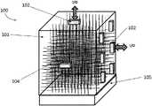
- FIG. 1depicts an exemplary embodiment in the form of an apparatus 100 for storing data in motion using a cubic cavity 101 .
- the cavity wallsmay be opaque and may not be necessarily transparent or semi-transparent
- FIG. 1depicts the cubic cavity 101 as if its cavity walls are transparent so as to show electromagnetic wave signals 104 traversing between the interior surfaces of the cavity within the inside of the cavity.
- the electromagnetic wave signalsare contained within the inside of the cavity 101 by undergoing a series of reflections or traversals between the interior surfaces of the cavity.
- Some or all portions of the interior surface of each of the six sides of the cubic cavity 101may be reflecting to allow reflections of the incident electromagnetic wave signals. In embodiments, some portions of the interior surfaces of the cavity may be non-reflecting and instead opaque or transparent to facilitate the operational design of the apparatus.
- the interior surfaces of the cavity 101may use any kind of reflective elements or material, such as mirrors, reflecting coatings, to name a few, or gratings, or any other photonic microstructure materials configured to reflect, regenerate, separate, and/or process the incident electromagnetic wave signal.
- the reflectivity of a surfaceis defined by the power of the reflected light or electromagnetic wave signal (P r ) divided by the power of the incident light or electromagnetic wave signal (P i ), and is less than or equal to 1. In embodiments, the reflectivity of the interior surfaces of the cubic cavity 101 is as close as possible to 1.
- the exemplary apparatus 100 for storing electromagnetic wave signalsmay include one or more optical processing units (OPUs or “tap points”) 102 .
- Each OPU 102may be configured to function as an input/output (I/O) port to receive electrical signals, such as digital data, to store in the cavity 101 as electromagnetic wave signals and access and retrieve the stored electromagnetic wave signals from the cavity 101 .
- I/Oinput/output
- the number and locations of the OPUs for the apparatusare not limited to those shown in FIG. 1 , and can be arbitrary and flexible to accommodate any number and arrangement of computing units, devices, and/or data centers coupled to the apparatus.
- one or more OPUs 102can be located inside the cavity 101 .
- Each OPU 102may include multiple function sub-assemblies and may contain one or more of transmitter, receiver, regenerator and other functional sub-assemblies for electronic and/or photonic processing.
- the general purpose of the transmitteris to write data into the cavity 101 .
- the transmittermay be configured to transform an electrical signal, such as digital data, into an electromagnetic wave signal 104 carrying data in motion, using, for example, laser light.
- the transmittermay comprise a laser and a modulator, or a directly modulated laser. Different wavelengths for the laser may be used for the electromagnetic wave signal as long as they are within the reflection window of the cavity 101 .
- the OPU 102may contain as many transmitters as needed.
- Each transmittermay also contain as many digital and/or photonic sub-assemblies as needed to modulate the electromagnetic wave signal 104 with any complex format and/or to generate any transverse spatial mode for beam shape of the electromagnetic wave signal.
- a receivermay comprise a photodetector configured to transform the electromagnetic wave signal 104 into an electrical signal, such as electronic digital data.
- the OPU 102may contain as many receivers as needed. Each receiver may also contain digital and/or photonic sub-assemblies for error correction or other digital processing purposes.
- the OPU 102may also include one or more regenerators configured to regenerate the electromagnetic wave signal 104 traveling in the cavity 101 .
- the regeneratormay be configured to re-amplify and/or re-time and/or re-shape the electromagnetic wave signal.
- the regeneratormay also be configured to implement error correction to restore lost information (e.g., lost bits of data) in the electromagnetic wave signal.
- the regeneratormay comprise an all-optical regenerator or an optoelectronic regenerator.
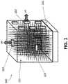
- FIG. 2provides a schematic diagram of an OPU 102 in accordance with an exemplary embodiment.
- electronic digital datais input to or output from the OPU 102 through a digital bus 201 .
- the digital bus 201is coupled to one or more transceivers 202 .
- Each transceiver 202may comprise at least one transmitter and at least one receiver.
- the OPU 102may include multiple transceivers corresponding to different wavelengths of the electromagnetic wave signals. Any wavelength and any number of different wavelengths may be used.
- the OPU 102may further include multiple transceivers corresponding to different spatial modes of the electromagnetic wave signals. Any spatial modes and any number of different spatial modes can be used.
- Each of the transceiver 202 - 1 - x through transceiver 202 -P-xmay be configured to transform the digital data received through the digital bus 201 into an electromagnetic wave signal having the corresponding wavelength ⁇ 1 , . . . , or ⁇ P .
- each transceivercan put the electronic or electrical signal on the electromagnetic wave signal using any of the modulation schemes (e.g., QAM, NRZ, QPSK, etc.) and/or any of the digital signal processing techniques (e.g., error correction, etc.) known to those of ordinary skill in the art that are necessary to ensure error-free propagation of the data within the cavity.
- the OPU 102may also include one or more wavelength division multiplexers/demultiplexers.
- FIG. 2shows that the OPU 102 includes multiple wavelength division multiplexers/demultiplexers 203 - 1 , . . . . , 203 -M, each corresponding to one of M different spatial modes of the electromagnetic wave signal.
- Each wavelength division multiplexer 203may be configured to combine different electromagnetic wave beams of distinct wavelengths into a single electromagnetic wave beam, while each wavelength division demultiplexer 203 may be configured for the reverse function, i.e., separating an electromagnetic wave beam containing many wavelengths into electromagnetic wave beams of distinct wavelengths.
- Each wavelength division multiplexer/demultiplexermay be implemented by using a set of filters, prisms, resonators, and/or gratings, which are configured to redirect an electromagnetic wave beam based on its wavelength.
- the beam shaper 204may comprise a liquid-crystal-based spatial light modulator, which can be reprogrammed.
- the beam shaper 204may comprise a phase mask having reflective or transparent surfaces that can modify the phase of the electromagnetic wave beam with respect to its transverse spatial location.
- the OPU 102may also include a spatial mode multiplexer/demultiplexer 205 .
- a spatial mode multiplexer 205may be configured to combine electromagnetic wave beams of different beam profiles (e.g., having different transverse spatial modes) into a single beam containing all of the incoming beam profiles (e.g., transverse spatial modes).
- a spatial mode demultiplexer 205may be configured to perform the reverse function, i.e., separating an electromagnetic wave beam containing many beam profiles (e.g., transverse spatial modes) into electromagnetic wave beams having distinct beam profiles (e.g., transverse spatial modes).
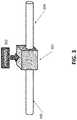
- the regenerator 301is configured to allow efficient energy transfer from a pump 302 to the electromagnetic wave signal 304 .
- the pumping of the crystal in the regenerator 301may be conducted through electricity or by an optical laser attached to the crystal.
- the crystal of the regenerator 301may be highly nonlinear or eventually doped with fluorescent elements.
- the regenerator 301may be an all-optical regenerator or an optoelectronic regenerator.
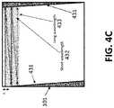
- FIG. 4Athere is depicted a cross-sectional view of the interior surfaces 402 of two opposing sides of the cubic cavity 101 , illustrating an electromagnetic wave beam 401 traversing between the interior surfaces in accordance with an exemplary embodiment of the present invention.
- the electromagnetic wave beam 401has a transversal spot size (or a diameter if the electromagnetic wave beam is circular) of s.
- the spot of the electromagnetic wave beammay be of any shape depending on the transverse spatial mode or beam shape of the electromagnetic wave beam 401 .
- a set of tilted mirrors 402may be placed on each of the two opposing sides of the cubic cavity 101 .
- Each of these mirrors 402may be configured to reflect the incident electromagnetic wave beam to the next mirror on the opposite side in such a way that the electromagnetic wave beam 401 travels between the interior surfaces on two opposing sides of the cubic cavity 101 in a zig-zag manner as shown in FIG. 4A .
- the mirrors 402may be further configured to reflect the incident electromagnetic wave beam to the next mirror on the opposite side such that the electromagnetic wave beam 401 travels in a zig-zag manner in a plane that is substantially perpendicular to the two opposing sides of the cubic cavity 101 .
- the cavity 101may further include a signal directing device or element configured to direct the traveling electromagnetic wave beam to a different direction.
- a signal directing element 404may be placed at the corner diagonally opposite to the point 403 where the electromagnetic wave beam was introduced into the inside of the cavity 101 , as shown in FIG. 4A .
- the signal directing element 404may be configured to direct the electromagnetic wave beam 401 by an angle (e.g., angle ⁇ ) with respect to a plane perpendicular to the plane of the electromagnetic wave beam propagation 401 shown in FIG. 4A .
- the signal directing element 404may comprise a mirror, which is slightly larger than the electromagnetic wave beam size and may be placed adjacent to the corner and tilted at the angle (e.g., angle ⁇ ) with respect to the plane of the electromagnetic wave beam propagation 401 .
- the signal directing element 404may comprise other optical elements or materials, such as transparent materials having refractive indices designed to direct the electromagnetic wave beam in a desired manner, waveguides, gradient index (GRIN) materials, prisms, or any suitable combination of any of these elements and materials. While these optical materials and elements may be limited in bandwidth, using a suitable combination of these materials and elements would overcome their limitations.
- the electromagnetic wave beammay be directed by the signal directing element 404 to another signal directing element on the opposite side of the cube, for example, a mirror 405 tilted at angle ⁇ with respect to a plane parallel to the plane of the previous electromagnetic wave beam propagation as shown in FIG. 4B .
- This signal directing element 405may be configured to direct the electromagnetic wave beam by, for example, angle ⁇ such that the propagation of the electromagnetic wave beam becomes parallel to the plane of its previous propagation as shown in FIG. 4A .
- the electromagnetic wave beam 401starts traveling in a next plane, which is parallel to and adjacent to the plane of its previous propagation in FIG. 4A , in a zig-zag manner by being reflected by mirrors 402 shown in FIG. 4B .
- the cavity 101may further comprise additional signal directing elements such that the electromagnetic wave beam 401 may sweep the volume of the cubic cavity 101 in one direction by repeating the above-described process of reflection (e.g., zig-zagging in x-y plane) and directing to the next level (e.g., directed in z-direction by signal directing elements 404 , 405 ).
- additional signal directing elementssuch that the electromagnetic wave beam 401 may sweep the volume of the cubic cavity 101 in one direction by repeating the above-described process of reflection (e.g., zig-zagging in x-y plane) and directing to the next level (e.g., directed in z-direction by signal directing elements 404 , 405 ).
- the cavity 101may further comprise additional signal directing elements configured to direct the electromagnetic wave beam in a direction perpendicular to the previous propagation direction such that, when the volume of the cubic cavity 101 has been swept by the electromagnetic wave beam in one direction, the signal directing elements may be configured to direct the electromagnetic wave beam to propagate in a plane (e.g., x-z plane) within the cubic cavity that is perpendicular to the initial plane of propagation (e.g., x-y plane).
- a mirror slightly larger than the electromagnetic wave beam sizemay be placed to direct the electromagnetic wave beam by 90°.
- the mirroris tilted at an angle of 45° with respect to the side wall of the cavity, which is parallel to the direction of the incoming electromagnetic wave beam.
- the signal directing elementsmay comprise other optical elements or materials, such as transparent materials having refractive indices designed to direct the electromagnetic wave beam in a desired manner, waveguides, gradient index (GRIN) materials, prisms, or any suitable combination of any of these elements and materials. While these optical materials and elements may be limited in bandwidth, using a suitable combination of these materials and elements would overcome their limitations.
- the propagation of the electromagnetic wave beam in a plane perpendicular to the initial plane of electromagnetic wave beam propagationmay be achieved by reflections between mirrors placed on the other two different sides of the cube in an arrangement analogous to what is shown in FIG. 4A .
- other signal directing elementsmay be provided in the cavity 101 to direct the electromagnetic wave beam in a perpendicular direction such that the electromagnetic wave beam propagates in a plane (e.g., zig-zagging in y-z plane) perpendicular to the two planes of propagation (e.g., x-y and x-z planes) previously used by the electromagnetic wave beam.
- the electromagnetic wave beammay sweep the cavity 101 a third time in a direction perpendicular to the two previous sweeps.
- additional signal directing elementssuch as a mirror positioned perpendicular to the direction of the electromagnetic wave beam propagation, may be used to reflect the electromagnetic wave beam in the opposite direction such that the electromagnetic wave beam can start sweeping the volume of the cubic cavity 101 in reverse directions another three times.
- the electromagnetic wave beam 401bounces 2c/s times from the interior surfaces 402 and travels approximately a distance of c after each bounce.
- the path length of the electromagnetic wave beam per planeis 2c 2 /s.
- various optical apparatusmay be used in the cavity to refocus or reshape the electromagnetic wave beam traveling within the cavity.
- one or more of lenses, gratings, metamaterials, and other optical elements or materials configured to modify the wave-fronts of the electromagnetic wave beammay be used to construct such optical apparatus.
- the beam size of the electromagnetic wave signalmay be an important factor in the data storage capacity of the cavity.
- the beam waist of an electromagnetic wave beam as a function of distance Ris given by (1):
- the reflecting surfacemay be used to focus the electromagnetic wave beam between the two reflecting surfaces, instead of using a curved surface to restore the reflected electromagnetic wave to a collimated wave.
- the electromagnetic wave beamhas the same size on the opposite reflecting surface instead of being larger by a factor of ⁇ 2.
- FIG. 6shows that the electromagnetic wave beam size is the same on both sides of the focal spot.
- spatial modessuch as OAM modes
- Gaussian modesmay be used along with Gaussian modes to increase data storage capability.
- Such fundamental Gaussian beamsare electromagnetic wave beams with the lowest known divergence. If OAM modes are used, then the electromagnetic wave beam size may be set based on a design wavelength and many OAM modes may be included at shorter wavelengths, within the same beam size.
- the beam waist for OAM modes at any given rangeincreases as the square root of the absolute value of the OAM mode number L.
- an electromagnetic wave beam for a Gaussian mode with a certain design wavelengthmay be used for data storage.
- the beam sizemay be kept the same by using more OAM modes. The shorter the wavelength the more OAM modes can be used.
- electromagnetic wave signalsmay be stored within a cavity having two parallel reflecting plates facing each other with a distance of the Rayleigh range between them.
- data in motionmay be stored in the cavity by an electromagnetic wave beam traveling back and forth in one direction between the two reflecting plates.
- the diameter of the electromagnetic wave beamis expanded by a factor of ⁇ 2 when it hits the opposite plate.
- the far field angular diffraction limitneed not be used because the distance between the plates is at the transition between the near and far fields.
- the highest wavelengthwould range from 1 ⁇ m to 20 ⁇ m, which corresponds to an angle ranging from 5 ⁇ 10 ⁇ 4 radians to 10 ⁇ 2 radians.
- the signal focusing devicemay comprise one or more layers of gradient index (GRIN) materials.
- FIG. 4Dshows how the signal focusing device 453 made of multiple layers of GRIN materials distinguish and separate overlapping incoming electromagnetic wave beam 451 and outgoing electromagnetic wave beam 452 and focus them to separate points on the interior surface 454 of the cavity in accordance with an exemplary embodiment.
- GRINgradient index
- FIG. 4Eis a cross-sectional view of interior surfaces 443 on two opposing sides of the cubic cavity 101 with signal focusing devices 442 placed either thereon or adjacent thereto in accordance with an exemplary embodiment.
- FIG. 4Eshows that the electromagnetic wave beam 441 is redirected at every bounce from the interior surface 443 and the signal focusing device 442 .
- the signal focusing devices 442are configured to distinguish two overlapping electromagnetic wave beams and focus them on different locations on the interior surfaces 443 .
- the signal focusing devicescan be replaced by or used in combination with other optical elements, such as a special geometry of mirrors configured to focus the beam on either side of the cavity, and/or photonic crystal structures like holes in the signal focusing devices, and/or diffraction structures to achieve a desired optical effect.
- the Gaussian electromagnetic wave beamsmay be partially superimposed during flight in the cavity as long as they become distinct at the recovery point.
- a combination of mirrors at different angles and/or signal focusing devicescould be used.
- FIG. 4Fis a cross-sectional view of the cubic cavity 101 in accordance with another exemplary embodiment.
- a combination of a signal focusing device 462 and a continuous mirror plate 464 tilted at an angleis placed, while on the opposite side of the cavity 101 , a combination of mirrors 463 , 465 tilted at different angles is placed.
- This exemplary embodimentis configured to discretize an overlapping electromagnetic wave beam 461 to a distinct electromagnetic wave beam at the transceiver.
- a plurality of parallel platesmay be placed within the inside of the cavity.
- Each side of each of the platesmay comprise, in part or in full, a reflective surface or a surface having a reflective element disposed thereon.
- Each of the reflective surfaces and reflective elementsmay comprise any kind of reflective elements or materials, such as mirrors, reflective coatings, to name a few, or gratings, or any other photonic microstructure materials configured to reflect, regenerate, separate, and/or process the incident electromagnetic wave signal.
- these parallel plates 471may be positioned substantially equidistant from each other within the inside of a cubic cavity 101 , as shown in FIG. 4G . These plates may be positioned along any of the three perpendicular directions that are parallel to a cube face.
- a second set of parallel platesmay be further added in the cavity along one of the other two perpendicular directions that are parallel to a cube face.
- the second set of parallel platesmay be placed substantially equidistant from each other.
- a third set of parallel platesmay be further added in the cavity, wherein the third set of parallel plates are perpendicular to the first and second sets of parallel plates.
- the third set of parallel platesmay be placed substantially equidistant from each other.
- Each side of each of the second and third sets of parallel platesmay comprise, in part or in full, a reflective surface or a surface having a reflective element disposed thereon.
- Each of the reflective surfaces and reflective elementsmay comprise any kind of reflective elements or materials, such as mirrors, reflective coatings, to name a few, or gratings, or any other photonic microstructure materials configured to reflect, regenerate, separate, and/or process the incident electromagnetic wave signal.
- the first, second and third sets of parallel platesmay together define a plurality of sub-cavities. Some or all of these sub-cavities may be configured to contain an electromagnetic wave signal.
- the distance between two parallel plates 471is c/N for (N+1) plates in the cavity.
- the size of electromagnetic wave beamsis reduced, because the Rayleigh range is shorter.
- the exemplary embodiment using (N+1) parallel plates arrayed in one directionmay increase the data storage capacity of the cubic cavity by a factor of (2+N)/3.
- FIGS. 7A and 7Bthere are depicted exemplary embodiments in the form of apparatuses for storing electromagnetic wave signals, such as data in motion, using rectangular shaped cavities 701 and 702 , each with length l, height h and width w.
- rectangular shaped cavities 701 and 702each with length l, height h and width w.
- preferably all directions and interior surfaces of the rectangular shaped cavity 701 , 702are configured to maximize the data storage capacity.
- the optical path lengthwould be reduced by a factor of 3 and the number of bounces would decrease from 4 hw/s 2 +4 lw/s 2 +4 hl/s 2 to 4 hw/s 2 , which can be significant when the length l of the rectangular shaped cavity 701 is large compared to its width w and height h, as shown in FIG. 7A .
- Reduction in the number of bouncescan reduce the absorption of the electromagnetic wave beam energy from the mirrors in the interior surfaces of the cavity if their reflectivity is less than 1. As a result, there is a reduced need for regenerators and a reduced amount of consumed power.
- FIG. 7Bshows a rectangular shaped cavity 702 where its length l is short compared to its width w and height h. Such a short rectangular shaped cavity 702 of FIG. 7B still has the same storage time for the electromagnetic wave signal traveling within the cavity as the longer rectangular shaped cavity 701 of FIG. 7A .
- signal focusing devices of different optical materials with different refractive indexessuch as GRIN materials, as well as gratings, lenses, photonic structures, diffraction structures, metamaterials and/or special geometry of mirrors may be used in a rectangular shaped cavity 701 , 702 to separate the overlapping electromagnetic wave beams, or refocus the electromagnetic wave beam on the cavity walls.
- a plurality of parallel platescan be placed within the rectangular shaped cavity 701 , 702 in one or more of the three perpendicular directions to increase the data storage capacity.
- regeneratorsmay be placed along the optical path within the rectangular shaped cavity 701 , 702 and used to restore the electromagnetic wave signal to its original state and/or compensate for any degradation.
- an optical apparatusmay be used to refocus or reshape the electromagnetic wave beam traveling within the rectangular shaped cavity 701 , 702 .
- Such optical apparatusmay comprise a combination of lenses, gratings, metamaterials, or optical materials or elements configured to modify the wave-fronts of the electromagnetic wave beam.
- an apparatus for storing electromagnetic wave signalsmay use a tube cavity.
- an electromagnetic wave beamwhich can be collimated or diffracting, may be injected into the tube cavity at any angle.
- the tube cavitymay comprise internal mirrors and/or other optical elements configured to redirect the electromagnetic wave beam.
- an optical path of arbitrary lengthmay be constructed.
- FIG. 8is a cross-sectional view of the base 802 of a tube cavity 801 .
- the tube cavity 801has a length l and its base has a diameter d.
- signal focusing devicesof different optical materials with different refractive indexes, such as GRIN materials, as well as gratings, lenses, metamaterials, and/or special geometry of mirrors may be used in a tube cavity 801 to separate the overlapping electromagnetic wave beams, or refocus the electromagnetic wave beam on the cavity walls.
- regeneratorsmay be placed along the optical path within the tube cavity 801 and used to restore the electromagnetic wave signal to its original state and/or compensate for any degradation.
- an optical apparatusmay be used to refocus or reshape the electromagnetic wave beam traveling within the tube cavity 801 .
- Such optical apparatusmay comprise a combination of lenses, gratings, metamaterials, or optical materials or elements configured to modify the wave-fronts of the electromagnetic wave beam.
- an apparatus for storing electromagnetic wave signalsmay use an egg-shaped cavity.
- an electromagnetic wave beam carrying data in motionmay enter the egg-shaped cavity at any angle. Depending on the angle of entry, the electromagnetic wave beam may travel a path of desired optical length within the egg-shaped cavity.
- FIG. 9is a cross-section view of an egg-shaped cavity 901 having ellipsoidal curved reflective interior surface 162 in accordance with an exemplary embodiment.
- the input/output couplere.g., OPU
- the input/output couplermay be a partially transmissive portion 161 of the reflective surface 162 which allows an input beam 163 into the cavity and couples an appropriate fraction of the power in the cavity out each round trip as the output beam 164 .
- an eraser 103 and a gain medium 153may be provided within the cavity in the path of the signal beam.
- a nonlinear filter and/or multiplexing elementsmay also be provided in the cavity system.
- signal focusing devices of different optical materials with different refractive indexessuch as GRIN materials, as well as gratings, lenses, metamaterials, and/or special geometry of mirrors may be used in the egg-shaped cavity 901 to separate the overlapping electromagnetic wave beams, or refocus the electromagnetic wave beam on the cavity walls.
- regeneratorsmay be placed along the optical path within the egg-shaped cavity 901 and used to restore the electromagnetic wave signal to its original state and/or compensate for any degradation.
- an optical apparatusmay be used to refocus or reshape the electromagnetic wave beam traveling within the egg-shaped cavity 901 .
- Such optical apparatusmay comprise a combination of lenses, gratings, metamaterials, or optical materials or elements configured to modify the wave-fronts of the electromagnetic wave beam.
- an apparatus for storing electromagnetic wave signalsmay use a resonating cavity, which is configured to create resonance at one or more frequencies of the electromagnetic wave signal.
- the resonating cavitymay be of any size and shape as long as it is configured to create resonance at one or more frequencies of the electromagnetic wave signal.
- cubic cavity, rectangular shaped cavity, tube cavity and egg-shaped cavitymay each be made resonating by aligning precisely the frequencies of the electromagnetic wave signal with a multiple of the inverse of the round trip of the cavity.
- all electromagnetic wave signal frequenciesconstructively interfere while any spurious frequencies would be diminished by destructive interference. Storage of data in motion in a resonating cavity may be useful in the case where amplifiers are used to compensate for loss.
- electromagnetic wavesinclude acoustic waves. Accordingly, storage in motion of information or any kind of data can also be implemented using acoustic (i.e., sound) waves.
- acoustic (i.e., sound) wavesRepresentative values for the speed of sound include about 1,500 m/sec in water, about 330 m/sec in air, and about 6,000 m/sec in steel. (There are a range of velocities for each case.)
- sound wavescan be in the region of tens of MHz. For example, some medical ultrasound devices operate in the regions of tens of MHz. Usually, lower frequency sound also has less attenuation over distance.
- Acoustic wavesrequire some medium in order to propagate.
- Information or any kind of datacan be transmitted and/or reflected between structures or within structures using acoustic waves in various transmission media (e.g., air and steel, to name a few).
- Embodiments of storage in motion using acoustic wavescould be constructed using such media.
- railroad trackscould be a long-distance medium.
- Acoustic wavescan be generated using various sources of vibration, including crystal transducers and speakers, to name a few.
- Microphonesdetect acoustic waves.
Landscapes
- Physics & Mathematics (AREA)
- General Physics & Mathematics (AREA)
- Optics & Photonics (AREA)
- Optical Modulation, Optical Deflection, Nonlinear Optics, Optical Demodulation, Optical Logic Elements (AREA)
- Optical Communication System (AREA)
- Geophysics And Detection Of Objects (AREA)
- Radar Systems Or Details Thereof (AREA)
- Optical Recording Or Reproduction (AREA)
Abstract
Description
and where λ is the wavelength of the electromagnetic wave beam and Rfis the Rayleigh range.
D=3√(λRf/π), (2)
D=3√(λRf(√L)/π), (3)
with the assumption that the electromagnetic wave beam diameter is the same on both ends of the link.
Claims (50)
Priority Applications (1)
| Application Number | Priority Date | Filing Date | Title |
|---|---|---|---|
| US16/529,479US11361794B2 (en) | 2018-08-02 | 2019-08-01 | Apparatus and method for storing wave signals in a cavity |
Applications Claiming Priority (2)
| Application Number | Priority Date | Filing Date | Title |
|---|---|---|---|
| US201862713735P | 2018-08-02 | 2018-08-02 | |
| US16/529,479US11361794B2 (en) | 2018-08-02 | 2019-08-01 | Apparatus and method for storing wave signals in a cavity |
Publications (2)
| Publication Number | Publication Date |
|---|---|
| US20200043522A1 US20200043522A1 (en) | 2020-02-06 |
| US11361794B2true US11361794B2 (en) | 2022-06-14 |
Family
ID=69227537
Family Applications (1)
| Application Number | Title | Priority Date | Filing Date |
|---|---|---|---|
| US16/529,479Active2039-10-04US11361794B2 (en) | 2018-08-02 | 2019-08-01 | Apparatus and method for storing wave signals in a cavity |
Country Status (12)
| Country | Link |
|---|---|
| US (1) | US11361794B2 (en) |
| EP (1) | EP3834019A4 (en) |
| JP (1) | JP2021532526A (en) |
| KR (1) | KR102454780B1 (en) |
| CN (1) | CN112654899A (en) |
| AU (2) | AU2019312672A1 (en) |
| BR (1) | BR112020024891A8 (en) |
| CA (1) | CA3101811A1 (en) |
| IL (1) | IL279031A (en) |
| MX (1) | MX2020013441A (en) |
| SG (1) | SG11202011983WA (en) |
| WO (1) | WO2020028716A1 (en) |
Families Citing this family (4)
| Publication number | Priority date | Publication date | Assignee | Title |
|---|---|---|---|---|
| CN115622657A (en)* | 2021-07-12 | 2023-01-17 | 宁波环球广电科技有限公司 | Multichannel wavelength division multiplexing light emitting device and optical transceiver |
| CN115622629A (en)* | 2021-07-12 | 2023-01-17 | 宁波环球广电科技有限公司 | Multichannel parallel optical communication module and optical transceiver |
| CN113777713B (en)* | 2021-08-04 | 2024-03-12 | 深圳市深光谷科技有限公司 | Integrated mode multiplexing optical chip |
| US11575429B1 (en) | 2022-07-08 | 2023-02-07 | Greenerwave | Multi-beam and multi-polarization electromagnetic wavefront shaping |
Citations (185)
| Publication number | Priority date | Publication date | Assignee | Title |
|---|---|---|---|---|
| US3141153A (en) | 1961-10-20 | 1964-07-14 | Beckman Instruments Inc | Immediate sequential access memory |
| US3164809A (en) | 1963-10-01 | 1965-01-05 | Gen Dynamics Corp | Self-synchronizing delay line data recirculation loop |
| US3229258A (en) | 1961-07-18 | 1966-01-11 | Harry L Heibeck | Digital storage system |
| US3277450A (en) | 1961-01-11 | 1966-10-04 | Gen Electric | High speed information storage system |
| US3350697A (en) | 1965-02-24 | 1967-10-31 | Collins Radio Co | Storage means for receiving, assembling, and distributing teletype characters |
| US3411142A (en) | 1965-12-27 | 1968-11-12 | Honeywell Inc | Buffer storage system |
| US4014166A (en) | 1976-02-13 | 1977-03-29 | The United States Of America As Represented By The Secretary Of Commerce | Satellite controlled digital clock system |
| US4136929A (en) | 1974-11-29 | 1979-01-30 | Hitachi, Ltd. | Apparatus for generating light pulse train |
| US4166212A (en) | 1977-06-03 | 1979-08-28 | International Standard Electric Corporation | Recirculating optical delay line |
| US4180814A (en) | 1978-03-13 | 1979-12-25 | International Standard Electric Corporation | Multiple beam receiving array signal processor |
| US4359733A (en) | 1980-09-23 | 1982-11-16 | Neill Gerard K O | Satellite-based vehicle position determining system |
| EP0080841A2 (en) | 1981-12-01 | 1983-06-08 | The Board Of Trustees Of The Leland Stanford Junior University | Dual coupler fiber optic recirculating memory |
| US4455651A (en) | 1980-10-20 | 1984-06-19 | Equatorial Communications Company | Satellite communications system and apparatus |
| US4469397A (en) | 1982-09-29 | 1984-09-04 | Board Of Trustees Of The Leland Stanford Junior University | Fiber optic resonator |
| US4473270A (en) | 1981-10-23 | 1984-09-25 | Leland Stanford Junior University | Splice-free fiber optic recirculating memory |
| EP0174540A2 (en) | 1984-09-14 | 1986-03-19 | Geostar Corporation | Satetellite-based position determination and message transfer system with monitoring of link quality |
| US4586779A (en) | 1982-05-28 | 1986-05-06 | Thomson-Csf | Device for memory-storage of a coherent image in a multitude optical cavity |
| US4588255A (en) | 1982-06-21 | 1986-05-13 | The Board Of Trustees Of The Leland Stanford Junior University | Optical guided wave signal processor for matrix-vector multiplication and filtering |
| US4653042A (en) | 1983-10-25 | 1987-03-24 | Thomson-Csf | Device for storing information in an optical fiber transmission system |
| US4652079A (en) | 1983-08-26 | 1987-03-24 | The Board Of Trustees Of The Leland Stanford Junior University | High speed pulse train generator |
| US4656666A (en) | 1979-10-01 | 1987-04-07 | Piekenbrock Lawrence J | Method and apparatus for handling information |
| US4708421A (en) | 1985-02-08 | 1987-11-24 | The Board Of Trustees Of The Leland Stanford Junior University | In-line fiber optic memory |
| US4738503A (en) | 1985-02-08 | 1988-04-19 | The Board Of Trustees Of The Leland Stanford Junion University | In-line fiber optic memory |
| US4815804A (en) | 1985-02-08 | 1989-03-28 | The Board Of Trustees Of The Leland Stanford Junior University | In-line fiber optic memory and method of using same |
| US4856862A (en) | 1988-04-22 | 1989-08-15 | Photonics Laboratories, Inc. | Optical storage method and apparatus |
| US4877952A (en) | 1988-10-11 | 1989-10-31 | American Telephone And Telegraph Company | Faser cavity optical memory with optical storage and readout |
| US4896948A (en) | 1989-02-21 | 1990-01-30 | International Business Machines Corporation | Simplified double-cavity tunable optical filter using voltage-dependent refractive index |
| US4923267A (en) | 1988-12-05 | 1990-05-08 | Gte Laboratories Incorporated | Optical fiber shift register |
| US4974931A (en) | 1989-11-13 | 1990-12-04 | At&T Bell Laboratories | Wavelength selective mode couplers |
| US5058060A (en) | 1988-12-05 | 1991-10-15 | Gte Laboratories Incorporated | Optical memory cell |
| US5144322A (en) | 1988-11-25 | 1992-09-01 | The United States Of America As Represented By The Secretary Of The Navy | Large-aperture sparse array detector system for multiple emitter location |
| JPH0572591A (en) | 1991-09-17 | 1993-03-26 | Nippon Telegr & Teleph Corp <Ntt> | Optical loop memory |
| US5319482A (en) | 1991-02-12 | 1994-06-07 | Nippon Telegraph And Telephone Corporation | Optical loop back and line test apparatus |
| US5335098A (en) | 1991-07-26 | 1994-08-02 | Accuwave Corporation | Fixing method for narrow bandwidth volume holograms in photorefractive materials |
| US5392154A (en) | 1994-03-30 | 1995-02-21 | Bell Communications Research, Inc. | Self-regulating multiwavelength optical amplifier module for scalable lightwave communications systems |
| WO1995008778A1 (en) | 1993-09-24 | 1995-03-30 | Grumman Aerospace Corporation | Navigation system using re-transmitted gps |
| US5440669A (en) | 1991-07-26 | 1995-08-08 | Accuwave Corporation | Photorefractive systems and methods |
| US5533154A (en) | 1991-10-18 | 1996-07-02 | British Telecommunications, Plc | Optical memory |
| US5555127A (en) | 1994-06-30 | 1996-09-10 | The Whitaker Corporation | Planar hybrid optical amplifier |
| US5566261A (en) | 1995-05-25 | 1996-10-15 | Massachusetts Institute Of Technology | Optical memory and data pattern generator |
| US5602838A (en) | 1994-12-21 | 1997-02-11 | Lucent Technologies Inc. | Global multi-satellite network |
| US5740117A (en) | 1994-09-15 | 1998-04-14 | International Business Machines Corporation | Optical memory for storing data |
| WO1998044512A1 (en) | 1997-03-27 | 1998-10-08 | British Telecommunications Public Limited Company | An optical memory |
| US5844700A (en) | 1996-07-24 | 1998-12-01 | The Board Of Trustees Of The Leland Stanford Junior University | Spatio-angular multiplexing geometry for volume holographic storage |
| US5862286A (en) | 1994-06-30 | 1999-01-19 | Hitachi, Ltd. | Optical memory device and optical circuit using optical memory device |
| US5896213A (en) | 1995-03-17 | 1999-04-20 | Nec Corporation | Optical fiber network system |
| US5978130A (en) | 1997-09-16 | 1999-11-02 | Mci Communications Corporation | Dual-band fiber optic amplification system using a single pump source |
| US5991069A (en) | 1998-01-22 | 1999-11-23 | Tyco Submarine Systems, Ltd. | Split-pumped dual stage optical fiber amplifier |
| US6002916A (en) | 1998-02-23 | 1999-12-14 | Lockheed Martin Corporation | Space-based server network architecture |
| US6035081A (en) | 1997-03-27 | 2000-03-07 | British Telecommunications Public Limited Company | Optical memory |
| US6043918A (en) | 1997-12-12 | 2000-03-28 | Stanford Telecommunications, Inc. | Laser satellite communication systems |
| EP0883322B1 (en) | 1997-06-03 | 2000-07-26 | Lucent Technologies Inc. | Optical-loop buffer that enhances the extinction ratio of the buffered signal |
| RU2155447C1 (en) | 1999-08-09 | 2000-08-27 | Открытое акционерное общество "Ракетно-космическая корпорация "Энергия" им.С.П.Королева" | Satellite system for data transmission between customer satellites and ground station |
| CA2266132A1 (en) | 1999-03-18 | 2000-09-18 | Terry A. Bisson | Satellite communication system |
| US6144486A (en) | 1998-01-30 | 2000-11-07 | Corning Incorporated | Pump wavelength tuning of optical amplifiers and use of same in wavelength division multiplexed systems |
| US6172926B1 (en) | 1999-12-17 | 2001-01-09 | Telcom Semiconductor, Inc. | Optical data storage devices and methods |
| US20010012142A1 (en) | 1995-02-28 | 2001-08-09 | Mitre Corporation | Laser satellite communication system |
| US6275479B1 (en) | 1999-03-19 | 2001-08-14 | Spacecode Llc | Multiplexed power amplifiers for satellite communication system |
| US6301037B1 (en) | 1997-03-07 | 2001-10-09 | Contraves Space Ag | Laser transmitting system for use in optical space communication systems |
| US6317232B1 (en) | 1998-03-25 | 2001-11-13 | Mci Communications Corporation | Bi-directional all-optical regenerator |
| US6317095B1 (en) | 1998-09-30 | 2001-11-13 | Anritsu Corporation | Planar antenna and method for manufacturing the same |
| US6347099B1 (en) | 1997-01-31 | 2002-02-12 | Corning Incorporated | Fiber lasers with shared pump |
| US6366356B1 (en) | 1999-04-01 | 2002-04-02 | Trw Inc. | High average power fiber laser system with high-speed, parallel wavefront sensor |
| US20020075536A1 (en) | 1998-06-30 | 2002-06-20 | Xiang-Dong Cao | Multi-wavelength all-optical regenerators ( mars) |
| US6437890B1 (en) | 1999-03-29 | 2002-08-20 | The United States Of America As Represented By The Secretary Of The Navy | Laser communications link |
| US6452719B2 (en) | 1996-05-31 | 2002-09-17 | Fujitsu Limited | Optical communication system and optical amplifier |
| US20020181342A1 (en) | 2001-05-30 | 2002-12-05 | Clark Bryan Kevin | Optical storage method and apparatus having enhanced resolution |
| WO2002097467A2 (en) | 2000-11-28 | 2002-12-05 | Lockheed Martin Corporation | System and method for adaptive broadcast radar system |
| US20020196488A1 (en) | 2001-06-21 | 2002-12-26 | Myers Michael H. | Recirculating frequency-stacking optical memory |
| US20030007230A1 (en) | 2001-06-20 | 2003-01-09 | Yasuhisa Kaneko | Optical signal storage |
| US6535314B1 (en) | 2000-01-13 | 2003-03-18 | Trw Inc. | Satellite optical communication beam acquisition techniques |
| US6580552B2 (en) | 2001-08-27 | 2003-06-17 | Jds Uniphase Corporation | Shared pump and serial rare earth doped fiber optical amplifiers |
| US20030128365A1 (en) | 2002-01-08 | 2003-07-10 | Honeywell International Inc. | Relative intensity noise controller for fiber light sources |
| US6609840B2 (en) | 2001-04-05 | 2003-08-26 | Alan Y. Chow | Wave length associative addressing system for WDM type light packet steering |
| US6647163B2 (en) | 2000-05-22 | 2003-11-11 | Shaowen Song | Optical memory apparatus and method |
| US20030219258A1 (en) | 2002-05-23 | 2003-11-27 | Ellis Andrew D. | Recovery of clock pulses of wavelength division multiplexed optical signals |
| US6674754B1 (en) | 1999-11-09 | 2004-01-06 | Synchrodyne Networks, Inc. | Wavelength division multiplexing combined with time division multiplexing using a common time reference |
| WO2004023192A2 (en) | 2002-09-09 | 2004-03-18 | Nile Mosley | Spatial optical memory |
| US20040151428A1 (en) | 2003-01-30 | 2004-08-05 | Nikonov Dmitri E. | Amplified optical splitter |
| EP1462883A2 (en) | 2003-03-27 | 2004-09-29 | Seiko Instruments Inc. | Chronograph timepiece |
| US20040190845A1 (en) | 2003-03-27 | 2004-09-30 | Datong Chen | Optical cache memory |
| US6826335B1 (en) | 1909-04-30 | 2004-11-30 | The University Of Southampton | Multi-fibre arrangements for high power fibre lasers and amplifiers |
| US6829439B1 (en)* | 2000-06-08 | 2004-12-07 | Meklyn Enterprises Limited | Optical communication device |
| US20040246583A1 (en) | 2001-12-14 | 2004-12-09 | Emmerich Mueller | Retro-reflecting device in particular for tunable lasers |
| US6839520B1 (en) | 1997-05-16 | 2005-01-04 | Contraves Space Ag | Method and arrangement for an interruption-proof optical satellite linkage |
| US6850364B2 (en) | 2002-06-12 | 2005-02-01 | Finisar Corporation | Method and apparatus for an optical multiplexer and demultiplexer with an optical processing loop |
| US20050084801A1 (en) | 2001-07-20 | 2005-04-21 | Idriss El-Hafidi | Photonics data storage system using a polypeptide material and method for making same |
| US6912075B1 (en) | 1999-05-17 | 2005-06-28 | The Directv Group, Inc. | Ring architecture for an optical satellite communication network with passive optical routing |
| US6930825B2 (en) | 2002-08-20 | 2005-08-16 | Red Sky Systems, Inc. | Method and apparatus for sharing pump energy from a single pump arrangement to optical fibers located in different fiber pairs |
| US6973271B2 (en) | 2000-10-04 | 2005-12-06 | Wave7 Optics, Inc. | System and method for communicating optical signals between a data service provider and subscribers |
| US20060173983A1 (en) | 2005-02-03 | 2006-08-03 | Fujitsu Limited | Information processing system and method of controlling information processing system |
| US7103239B2 (en) | 2001-10-09 | 2006-09-05 | Infinera Corporation | Optical transmitter |
| US7103280B1 (en) | 1999-06-05 | 2006-09-05 | The Directv Group, Inc. | Architecture for an optical satellite communication network |
| US7110651B2 (en) | 2004-08-19 | 2006-09-19 | Lucent Technologies Inc. | Optical fiber having enhanced separation of higher-order modes |
| WO2006101873A2 (en) | 2005-03-16 | 2006-09-28 | Ge Licensing, Inc. | Data storage devices and methods |
| US7149431B2 (en) | 2002-10-15 | 2006-12-12 | Samsung Electronics Co., Ltd. | Self-seeded Fabry-Perot laser device for wavelength division multiplexing system |
| US7167286B2 (en) | 2003-03-10 | 2007-01-23 | Inphase Technologies, Inc. | Polytopic multiplex holography |
| US7174067B2 (en) | 2001-12-06 | 2007-02-06 | Florida Institute Of Technology | Method and apparatus for spatial domain multiplexing in optical fiber communications |
| US7177510B2 (en) | 2004-08-09 | 2007-02-13 | Fitel Usa Corp. | Polarization insensitive microbend fiber gratings and devices using the same |
| US7180447B1 (en) | 2005-04-29 | 2007-02-20 | Lockhead Martin Corporation | Shared phased array beamformer |
| US20070072546A1 (en) | 2000-08-18 | 2007-03-29 | Northrop Grumman Space & Missions Systems Corp. | Satellite communication system |
| US20070081785A1 (en) | 2005-09-28 | 2007-04-12 | Hays Kirk I | Method, apparatus and system for global shared memory using serial optical memory |
| US7235150B2 (en) | 2001-02-14 | 2007-06-26 | Gemfire Corporation | Multi-channel laser pump source for optical amplifiers |
| US20080002981A1 (en) | 2000-05-04 | 2008-01-03 | The Directv Group, Inc. | Ground to space to ground trunking system |
| US20080008076A1 (en) | 2004-04-16 | 2008-01-10 | Raguin Daniel H | Calibration of Holographic Data Storage Systems Using Holographic Media Calibration Features |
| JP2008117446A (en) | 2006-11-01 | 2008-05-22 | Sony Corp | Optical pickup, optical disk device, polarization adjusting plate, and optical device |
| US20080144164A1 (en) | 2005-04-19 | 2008-06-19 | Eolite Systems | Device for Generating Laser Impulses Amplified by Optical Fibres Provided with Photon Layers |
| US20080239428A1 (en) | 2007-04-02 | 2008-10-02 | Inphase Technologies, Inc. | Non-ft plane angular filters |
| US7450618B2 (en) | 2001-01-30 | 2008-11-11 | Board Of Trustees Operating Michigan State University | Laser system using ultrashort laser pulses |
| US7542679B2 (en) | 2001-08-24 | 2009-06-02 | Broadwing Corporation | Optical transmission systems, devices, and method |
| US7557365B2 (en) | 2005-09-30 | 2009-07-07 | Virgin Islands Microsystems, Inc. | Structures and methods for coupling energy from an electromagnetic wave |
| US20090185175A1 (en)* | 2004-09-28 | 2009-07-23 | Honeywell International Inc. | Cavity ring down system having a common input/output port |
| US20090202191A1 (en) | 2008-02-12 | 2009-08-13 | Furukawa Electric North America, Inc. | Systems and Techniques for Generating Cylindrical Vector Beams |
| US20090219959A1 (en) | 2008-01-16 | 2009-09-03 | Pyrophotonics Lasers Inc. | Method and system for tunable pulsed laser source |
| US7729398B2 (en) | 2007-04-10 | 2010-06-01 | Northrop Grumman Systems Corporation | Error control for high-power laser system employing diffractive optical element beam combiner |
| US7733930B2 (en) | 2007-04-10 | 2010-06-08 | Northrop Grumman Systems Corporation | Error control for high-power laser system employing diffractive optical element beam combiner with tilt error control |
| US7742209B2 (en) | 2006-11-01 | 2010-06-22 | Inphase Technologies, Inc. | Monocular holographic data storage system architecture |
| US7742210B2 (en) | 2003-12-30 | 2010-06-22 | Stx Aprilis, Inc. | Replication of data to holographic medium using holographic master media |
| US7756169B2 (en) | 2008-01-23 | 2010-07-13 | Northrop Grumman Systems Corporation | Diffractive method for control of piston error in coherent phased arrays |
| US7796487B2 (en) | 2005-05-10 | 2010-09-14 | Seagate Technology Llc | Optical system for data storage devices |
| US20100269143A1 (en) | 2009-04-21 | 2010-10-21 | Irving Rabowsky | System and Method for Satellite Enhanced Command, Control, and Surveillance Services Between Network Management Centers and Unmanned Land and Aerial Devices |
| US20100279604A1 (en) | 2009-05-04 | 2010-11-04 | Cisco Technology, Inc. | Intersatellite Links |
| US7843791B2 (en) | 2006-11-08 | 2010-11-30 | Daewoo Electronics Corp. | Optical information processing method and optical information reproducing method using multiplexing schemes capable of improving a density of recorded optical information |
| US20100322058A1 (en) | 2009-06-18 | 2010-12-23 | Marvin Hutt | Holographic storage system using angle-multiplexing |
| US7950812B2 (en)* | 2006-01-11 | 2011-05-31 | Cubic Corporation | Shutters for infra red communication at moderate bandwidths |
| US8036537B2 (en) | 2007-06-13 | 2011-10-11 | International Business Machines Corporation | Optical pulse amplication apparatus and method |
| WO2011142849A2 (en) | 2010-01-21 | 2011-11-17 | Rudolph Wolfgang G | Gas filled hollow fiber laser |
| US20120063752A1 (en) | 2010-05-07 | 2012-03-15 | Cochran Don W | Corner-cube irradiation control |
| JP2012084630A (en) | 2010-10-08 | 2012-04-26 | Miyachi Technos Corp | Fiber laser processing device and laser diode for excitation power supply device |
| US20120188865A1 (en) | 2011-01-21 | 2012-07-26 | Commscope Inc. Of North Carolina | Intelligent Patching Systems and Methods Using Phantom Mode Control Signals and Related Communications Connectors |
| US8232028B2 (en) | 2008-07-24 | 2012-07-31 | Inphase Technologies, Inc. | Holographic storage medium and method for gated diffusion of photoactive monomer |
| US8305863B2 (en) | 2008-09-25 | 2012-11-06 | Kabushiki Kaisha Toshiba | Optical information recording apparatus |
| US8417125B2 (en) | 2009-06-02 | 2013-04-09 | Bae Systems Information And Electronic Systems Integration Inc. | Full-duplex laser communication using single wavelength from an optical transmitter |
| US20130120831A1 (en) | 2010-05-13 | 2013-05-16 | Oclaro Technology Limited | Optical amplifiers |
| US20130175450A1 (en) | 2010-10-14 | 2013-07-11 | James J. Scherer | Optical chamber module assembly |
| US20130216180A1 (en) | 2010-10-29 | 2013-08-22 | Michael Renne Ty Tan | Optical interconnect fabrics implemented with star couplers |
| US8532486B2 (en) | 2012-02-13 | 2013-09-10 | The United States Of America As Represented By The Secretary Of The Army | Method and apparatus for detecting radio-frequency signals using a dispersive fiber optical loop |
| US8582972B2 (en) | 2006-08-31 | 2013-11-12 | The Trustees Of Columbia University In The City Of New York | Systems and methods for storing optical data |
| US20130315590A1 (en) | 2013-05-01 | 2013-11-28 | U.S. Army Research Laboratory Attn: Rdrl-Loc-I | Method and Apparatus for Analyzing the Spectrum of Radio-Frequency Signals Using Unamplified Fiber Optic Recirculation Loops |
| WO2014029971A1 (en) | 2012-08-21 | 2014-02-27 | The Science And Technology Facilities Council | Method and apparatus for external cavity laser absorption spectroscopy |
| US8699888B2 (en) | 2011-02-24 | 2014-04-15 | Telefonaktiebolaget Lm Ericsson (Publ) | Optical linear feedback circuit |
| WO2014107696A1 (en) | 2013-01-07 | 2014-07-10 | The Trustees Of Columbia University In The City Of New York | Systems and methods for multilevel optical storage in tunable photonic crystal cavities |
| US20140334284A1 (en) | 2013-05-07 | 2014-11-13 | Electronics And Telecommunications Research Institute | Transmitter and receiver for wireless communication using revolution division multiplexing, and signal transmission and reception method thereof |
| US8913894B2 (en) | 2012-07-13 | 2014-12-16 | Raytheon Company | High-bandwidth optical communications relay architecture |
| US20150104141A1 (en) | 2011-12-19 | 2015-04-16 | Corning Incorporated | Uniform uv efficient light diffusing fiber |
| US9077577B1 (en) | 2014-04-04 | 2015-07-07 | Solyman Ashrafi | System and method for communication using orbital angular momentum with multiple layer overlay modulation |
| US20150244458A1 (en) | 2014-02-25 | 2015-08-27 | Google Inc. | Optical Communication Terminal |
| US9176280B2 (en) | 2013-10-21 | 2015-11-03 | Oracle International Corporation | Optical reflector based on a directional coupler and a coupled optical loop |
| US20160043794A1 (en) | 2014-08-08 | 2016-02-11 | Solyman Ashrafi | Systems and methods for focusing beams with mode division multiplexing |
| US20160204866A1 (en) | 2015-01-09 | 2016-07-14 | Don M. Boroson | Ground terminal design for high rate direct to earth optical communications |
| US20160204896A1 (en) | 2015-01-14 | 2016-07-14 | Zte Corporation | Time division multiplexed orbital angular momentum based communication |
| WO2016164038A1 (en) | 2015-04-10 | 2016-10-13 | Hewlett Packard Enterprise Development Lp | Optical zig-zags |
| US9503186B2 (en) | 2012-08-30 | 2016-11-22 | National Institute Of Information And Communications Technology | Space division multiplexing apparatus including multi-core fiber and selfhomodyne detection method |
| US20170034250A1 (en) | 2015-02-03 | 2017-02-02 | Shahraum Scott Sobhani | Space-based electronic data storage and transfer network system |
| US9570811B2 (en) | 2013-07-29 | 2017-02-14 | Fujitsu Limited | Device to reflect and transmit electromagnetic wave and antenna device |
| US9609402B2 (en) | 2015-03-26 | 2017-03-28 | Amazon Technologies, Inc. | Optical transmittal storage networks |
| US9625878B2 (en) | 2009-03-10 | 2017-04-18 | Drexel University | Dynamic time multiplexing fabrication of holographic polymer dispersed liquid crystals for increased wavelength sensitivity |
| US20170139079A1 (en) | 2015-07-23 | 2017-05-18 | Research Foundation Of The City University Of New York | Method for altering light interactions with complex structured light |
| US9712239B2 (en) | 2015-02-06 | 2017-07-18 | Florida Institute of Technology, Inc. | Method and apparatus for multiplexed optical communication system using spatial domain multiplexing (SDM) and orbital angular momentum of photon (OAM) multiplexing with wavelength division multiplexing (WDM) |
| US9749080B2 (en) | 2015-11-11 | 2017-08-29 | Google Inc. | TWDM passive network with extended reach and capacity |
| US9760061B2 (en) | 2013-01-23 | 2017-09-12 | Akonia Holographics Llc | Dynamic aperture holography |
| WO2017165429A1 (en) | 2016-03-22 | 2017-09-28 | Lonestar, LLC | Data in motion storage system and method |
| US20170302048A1 (en) | 2015-12-22 | 2017-10-19 | California Institute Of Technology | Stabilized non-reciprocal fiber-ring brillouin laser source |
| US9812845B1 (en) | 2016-11-21 | 2017-11-07 | Oracle International Corporation | Fast wavelength-tunable hybrid optical transmitter |
| US9843388B1 (en) | 2015-06-08 | 2017-12-12 | Amazon Technologies, Inc. | Laser communications |
| US9912409B2 (en) | 2016-04-12 | 2018-03-06 | Cable Television Laboratories, Inc | Fiber communication systems and methods |
| US9917646B2 (en) | 2016-06-15 | 2018-03-13 | Space Systems/Loral, Llc | High throughput satellite system with RF service uplink beams and optical feeder downlink beams |
| US20180131447A1 (en) | 2015-04-10 | 2018-05-10 | National Institute Of Information And Communications Technology | Polarization insensitive self-homodyne detection receiver for spatial-division multiplexing systems |
| US10001603B2 (en) | 2014-03-18 | 2018-06-19 | Politecnico Di Milano | Optical multiplexer/demultiplexer device comprising Porro prisms |
| US10073417B2 (en) | 2014-08-08 | 2018-09-11 | Nxgen Partners Ip, Llc | System and method for applying orthogonal limitations to light beams using microelectromechanical systems |
| US10084532B2 (en) | 2015-04-10 | 2018-09-25 | Viasat, Inc. | Access node farm for end-to-end beamforming |
| US10103799B2 (en) | 2015-03-16 | 2018-10-16 | Lockheed Martin Corporation | Apparatus and method for increased data rates in underwater communications using orbital angular momentum |
| US10122456B2 (en) | 2017-02-03 | 2018-11-06 | Space Systems/Loral, Llc | Ground based subsystems, for inclusion in optical gateway, and that interface with optical networks external to optical gateway |
| US10142012B2 (en) | 2015-03-11 | 2018-11-27 | The Aerospace Corporation | Co-orbiting laser communications relay satellite |
| US20190074893A1 (en) | 2016-04-28 | 2019-03-07 | Cloud Constellation Corporation | Intermediary satellite network for cross-strapping and local network decongestion |
| US10305560B2 (en) | 2016-01-20 | 2019-05-28 | Panasonic Intellectual Property Management Co., Ltd. | Transmission device, reception device, transmission method, and reception method |
| US10312999B2 (en) | 2016-03-23 | 2019-06-04 | The Boeing Company | High-capacity communications satellite using passive optical beamforming |
| US10326526B2 (en) | 2016-09-08 | 2019-06-18 | Nxgen Partners Ip, Llc | Method for muxing orthogonal modes using modal correlation matrices |
| US10411811B2 (en) | 2015-12-07 | 2019-09-10 | University Of Southern California | Systems and techniques for communication using combined orbital angular momentum and multiple-input-multiple-output processing |
| US20190334609A1 (en) | 2016-12-28 | 2019-10-31 | Intel Corporation | Orbital angular momentum-based multiplexing with shared antenna elements |
| US20200050959A1 (en) | 2018-08-07 | 2020-02-13 | Nxgen Partners Ip, Llc | Universal quantum computer, communication, qkd security and quantum networks using oam qu-dits with dlp |
| US10606146B2 (en) | 2017-11-24 | 2020-03-31 | Tesat-Spacecom Gmbh & Co. Kg | Beam orientation in unidirectional optical communication systems |
| WO2020144319A1 (en) | 2019-01-10 | 2020-07-16 | Deutsches Zentrum für Luft- und Raumfahrt e.V. | Structure for receiving an optical data signal |
| US20200277087A1 (en) | 2018-03-13 | 2020-09-03 | Cloud Constellation Corporation | Earth observation satellite information routing system |
| US10827911B2 (en) | 2016-06-03 | 2020-11-10 | Trustees Of Boston University | Optical imaging system employing vortex fiber for multiple-mode illumination |
Family Cites Families (11)
| Publication number | Priority date | Publication date | Assignee | Title |
|---|---|---|---|---|
| JPS61165889A (en)* | 1985-01-17 | 1986-07-26 | Fujitsu Ltd | Multiple spatial memory method |
| GB9024327D0 (en)* | 1990-11-08 | 1990-12-19 | British Telecomm | Optical memory |
| JPH0729390A (en)* | 1993-07-07 | 1995-01-31 | Nippon Telegr & Teleph Corp <Ntt> | Optical buffer memory |
| JPH0745091A (en)* | 1993-07-28 | 1995-02-14 | Nippon Telegr & Teleph Corp <Ntt> | Optical buffer memory |
| JP3699493B2 (en)* | 1994-03-09 | 2005-09-28 | アンリツ株式会社 | Optical memory |
| JPH0836897A (en)* | 1994-07-25 | 1996-02-06 | Nippon Telegr & Teleph Corp <Ntt> | Optical frequency multiplexing random access memory |
| JPH08125659A (en)* | 1994-10-25 | 1996-05-17 | Oki Electric Ind Co Ltd | Optical buffer memory device |
| JP2931226B2 (en)* | 1995-01-26 | 1999-08-09 | 浜松ホトニクス株式会社 | Optical feedback type photodetector |
| US5646396A (en)* | 1995-05-19 | 1997-07-08 | Richard; Jenkin A. | Optical position system |
| EP1769568A1 (en)* | 2004-07-16 | 2007-04-04 | University College Cork-National University of Ireland, Cork | Method for designing a semiconductor laser with intracavity reflecting features, semiconductor laser and method of fabrication thereof |
| US9570420B2 (en)* | 2011-09-29 | 2017-02-14 | Broadcom Corporation | Wireless communicating among vertically arranged integrated circuits (ICs) in a semiconductor package |
- 2019
- 2019-08-01JPJP2021504778Apatent/JP2021532526A/enactivePending
- 2019-08-01USUS16/529,479patent/US11361794B2/enactiveActive
- 2019-08-01KRKR1020217005587Apatent/KR102454780B1/enactiveActive
- 2019-08-01CNCN201980051096.5Apatent/CN112654899A/enactivePending
- 2019-08-01MXMX2020013441Apatent/MX2020013441A/enunknown
- 2019-08-01WOPCT/US2019/044744patent/WO2020028716A1/ennot_activeCeased
- 2019-08-01SGSG11202011983WApatent/SG11202011983WA/enunknown
- 2019-08-01BRBR112020024891Apatent/BR112020024891A8/ennot_activeIP Right Cessation
- 2019-08-01CACA3101811Apatent/CA3101811A1/enactivePending
- 2019-08-01EPEP19843160.3Apatent/EP3834019A4/ennot_activeWithdrawn
- 2019-08-01AUAU2019312672Apatent/AU2019312672A1/ennot_activeAbandoned
- 2020
- 2020-11-26ILIL279031Apatent/IL279031A/enunknown
- 2022
- 2022-10-28AUAU2022259842Apatent/AU2022259842A1/ennot_activeAbandoned
Patent Citations (199)
| Publication number | Priority date | Publication date | Assignee | Title |
|---|---|---|---|---|
| US6826335B1 (en) | 1909-04-30 | 2004-11-30 | The University Of Southampton | Multi-fibre arrangements for high power fibre lasers and amplifiers |
| US3277450A (en) | 1961-01-11 | 1966-10-04 | Gen Electric | High speed information storage system |
| US3229258A (en) | 1961-07-18 | 1966-01-11 | Harry L Heibeck | Digital storage system |
| US3141153A (en) | 1961-10-20 | 1964-07-14 | Beckman Instruments Inc | Immediate sequential access memory |
| US3164809A (en) | 1963-10-01 | 1965-01-05 | Gen Dynamics Corp | Self-synchronizing delay line data recirculation loop |
| US3350697A (en) | 1965-02-24 | 1967-10-31 | Collins Radio Co | Storage means for receiving, assembling, and distributing teletype characters |
| US3411142A (en) | 1965-12-27 | 1968-11-12 | Honeywell Inc | Buffer storage system |
| US4136929A (en) | 1974-11-29 | 1979-01-30 | Hitachi, Ltd. | Apparatus for generating light pulse train |
| US4014166A (en) | 1976-02-13 | 1977-03-29 | The United States Of America As Represented By The Secretary Of Commerce | Satellite controlled digital clock system |
| US4166212A (en) | 1977-06-03 | 1979-08-28 | International Standard Electric Corporation | Recirculating optical delay line |
| US4180814A (en) | 1978-03-13 | 1979-12-25 | International Standard Electric Corporation | Multiple beam receiving array signal processor |
| US4656666A (en) | 1979-10-01 | 1987-04-07 | Piekenbrock Lawrence J | Method and apparatus for handling information |
| US4359733A (en) | 1980-09-23 | 1982-11-16 | Neill Gerard K O | Satellite-based vehicle position determining system |
| US4455651A (en) | 1980-10-20 | 1984-06-19 | Equatorial Communications Company | Satellite communications system and apparatus |
| US4473270A (en) | 1981-10-23 | 1984-09-25 | Leland Stanford Junior University | Splice-free fiber optic recirculating memory |
| US4479701A (en) | 1981-12-01 | 1984-10-30 | Leland Stanford Junior University | Dual coupler fiber optic recirculating memory |
| EP0080841A2 (en) | 1981-12-01 | 1983-06-08 | The Board Of Trustees Of The Leland Stanford Junior University | Dual coupler fiber optic recirculating memory |
| US4586779A (en) | 1982-05-28 | 1986-05-06 | Thomson-Csf | Device for memory-storage of a coherent image in a multitude optical cavity |
| US4588255A (en) | 1982-06-21 | 1986-05-13 | The Board Of Trustees Of The Leland Stanford Junior University | Optical guided wave signal processor for matrix-vector multiplication and filtering |
| US4469397A (en) | 1982-09-29 | 1984-09-04 | Board Of Trustees Of The Leland Stanford Junior University | Fiber optic resonator |
| US4652079A (en) | 1983-08-26 | 1987-03-24 | The Board Of Trustees Of The Leland Stanford Junior University | High speed pulse train generator |
| US4653042A (en) | 1983-10-25 | 1987-03-24 | Thomson-Csf | Device for storing information in an optical fiber transmission system |
| EP0174540A2 (en) | 1984-09-14 | 1986-03-19 | Geostar Corporation | Satetellite-based position determination and message transfer system with monitoring of link quality |
| US4744083A (en) | 1984-09-14 | 1988-05-10 | Geostar Corporation | Satellite-based position determining and message transfer system with monitoring of link quality |
| US4738503A (en) | 1985-02-08 | 1988-04-19 | The Board Of Trustees Of The Leland Stanford Junion University | In-line fiber optic memory |
| US4815804A (en) | 1985-02-08 | 1989-03-28 | The Board Of Trustees Of The Leland Stanford Junior University | In-line fiber optic memory and method of using same |
| US4708421A (en) | 1985-02-08 | 1987-11-24 | The Board Of Trustees Of The Leland Stanford Junior University | In-line fiber optic memory |
| US4856862A (en) | 1988-04-22 | 1989-08-15 | Photonics Laboratories, Inc. | Optical storage method and apparatus |
| US4877952A (en) | 1988-10-11 | 1989-10-31 | American Telephone And Telegraph Company | Faser cavity optical memory with optical storage and readout |
| US5144322A (en) | 1988-11-25 | 1992-09-01 | The United States Of America As Represented By The Secretary Of The Navy | Large-aperture sparse array detector system for multiple emitter location |
| US4923267A (en) | 1988-12-05 | 1990-05-08 | Gte Laboratories Incorporated | Optical fiber shift register |
| US5058060A (en) | 1988-12-05 | 1991-10-15 | Gte Laboratories Incorporated | Optical memory cell |
| US4896948A (en) | 1989-02-21 | 1990-01-30 | International Business Machines Corporation | Simplified double-cavity tunable optical filter using voltage-dependent refractive index |
| US4974931A (en) | 1989-11-13 | 1990-12-04 | At&T Bell Laboratories | Wavelength selective mode couplers |
| US5319482A (en) | 1991-02-12 | 1994-06-07 | Nippon Telegraph And Telephone Corporation | Optical loop back and line test apparatus |
| US5335098A (en) | 1991-07-26 | 1994-08-02 | Accuwave Corporation | Fixing method for narrow bandwidth volume holograms in photorefractive materials |
| US5440669A (en) | 1991-07-26 | 1995-08-08 | Accuwave Corporation | Photorefractive systems and methods |
| JPH0572591A (en) | 1991-09-17 | 1993-03-26 | Nippon Telegr & Teleph Corp <Ntt> | Optical loop memory |
| US5533154A (en) | 1991-10-18 | 1996-07-02 | British Telecommunications, Plc | Optical memory |
| WO1995008778A1 (en) | 1993-09-24 | 1995-03-30 | Grumman Aerospace Corporation | Navigation system using re-transmitted gps |
| US5438337A (en) | 1993-09-24 | 1995-08-01 | Northrop Grumman Corporation | Navigation system using re-transmitted GPS |
| US5392154A (en) | 1994-03-30 | 1995-02-21 | Bell Communications Research, Inc. | Self-regulating multiwavelength optical amplifier module for scalable lightwave communications systems |
| US5555127A (en) | 1994-06-30 | 1996-09-10 | The Whitaker Corporation | Planar hybrid optical amplifier |
| US5862286A (en) | 1994-06-30 | 1999-01-19 | Hitachi, Ltd. | Optical memory device and optical circuit using optical memory device |
| US5740117A (en) | 1994-09-15 | 1998-04-14 | International Business Machines Corporation | Optical memory for storing data |
| US5602838A (en) | 1994-12-21 | 1997-02-11 | Lucent Technologies Inc. | Global multi-satellite network |
| US20010012142A1 (en) | 1995-02-28 | 2001-08-09 | Mitre Corporation | Laser satellite communication system |
| US6304354B2 (en) | 1995-02-28 | 2001-10-16 | The Mitre Corporation | Laser satellite communication system |
| US5896213A (en) | 1995-03-17 | 1999-04-20 | Nec Corporation | Optical fiber network system |
| US5566261A (en) | 1995-05-25 | 1996-10-15 | Massachusetts Institute Of Technology | Optical memory and data pattern generator |
| US6452719B2 (en) | 1996-05-31 | 2002-09-17 | Fujitsu Limited | Optical communication system and optical amplifier |
| US5844700A (en) | 1996-07-24 | 1998-12-01 | The Board Of Trustees Of The Leland Stanford Junior University | Spatio-angular multiplexing geometry for volume holographic storage |
| US6347099B1 (en) | 1997-01-31 | 2002-02-12 | Corning Incorporated | Fiber lasers with shared pump |
| US6301037B1 (en) | 1997-03-07 | 2001-10-09 | Contraves Space Ag | Laser transmitting system for use in optical space communication systems |
| US6035081A (en) | 1997-03-27 | 2000-03-07 | British Telecommunications Public Limited Company | Optical memory |
| WO1998044512A1 (en) | 1997-03-27 | 1998-10-08 | British Telecommunications Public Limited Company | An optical memory |
| US6839520B1 (en) | 1997-05-16 | 2005-01-04 | Contraves Space Ag | Method and arrangement for an interruption-proof optical satellite linkage |
| EP0883322B1 (en) | 1997-06-03 | 2000-07-26 | Lucent Technologies Inc. | Optical-loop buffer that enhances the extinction ratio of the buffered signal |
| US5978130A (en) | 1997-09-16 | 1999-11-02 | Mci Communications Corporation | Dual-band fiber optic amplification system using a single pump source |
| US6043918A (en) | 1997-12-12 | 2000-03-28 | Stanford Telecommunications, Inc. | Laser satellite communication systems |
| US5991069A (en) | 1998-01-22 | 1999-11-23 | Tyco Submarine Systems, Ltd. | Split-pumped dual stage optical fiber amplifier |
| US6144486A (en) | 1998-01-30 | 2000-11-07 | Corning Incorporated | Pump wavelength tuning of optical amplifiers and use of same in wavelength division multiplexed systems |
| US6002916A (en) | 1998-02-23 | 1999-12-14 | Lockheed Martin Corporation | Space-based server network architecture |
| US6317232B1 (en) | 1998-03-25 | 2001-11-13 | Mci Communications Corporation | Bi-directional all-optical regenerator |
| US20020075536A1 (en) | 1998-06-30 | 2002-06-20 | Xiang-Dong Cao | Multi-wavelength all-optical regenerators ( mars) |
| US6317095B1 (en) | 1998-09-30 | 2001-11-13 | Anritsu Corporation | Planar antenna and method for manufacturing the same |
| CA2266132A1 (en) | 1999-03-18 | 2000-09-18 | Terry A. Bisson | Satellite communication system |
| US6275479B1 (en) | 1999-03-19 | 2001-08-14 | Spacecode Llc | Multiplexed power amplifiers for satellite communication system |
| US6437890B1 (en) | 1999-03-29 | 2002-08-20 | The United States Of America As Represented By The Secretary Of The Navy | Laser communications link |
| US6366356B1 (en) | 1999-04-01 | 2002-04-02 | Trw Inc. | High average power fiber laser system with high-speed, parallel wavefront sensor |
| US6912075B1 (en) | 1999-05-17 | 2005-06-28 | The Directv Group, Inc. | Ring architecture for an optical satellite communication network with passive optical routing |
| US7103280B1 (en) | 1999-06-05 | 2006-09-05 | The Directv Group, Inc. | Architecture for an optical satellite communication network |
| RU2155447C1 (en) | 1999-08-09 | 2000-08-27 | Открытое акционерное общество "Ракетно-космическая корпорация "Энергия" им.С.П.Королева" | Satellite system for data transmission between customer satellites and ground station |
| US6674754B1 (en) | 1999-11-09 | 2004-01-06 | Synchrodyne Networks, Inc. | Wavelength division multiplexing combined with time division multiplexing using a common time reference |
| US6172926B1 (en) | 1999-12-17 | 2001-01-09 | Telcom Semiconductor, Inc. | Optical data storage devices and methods |
| US6535314B1 (en) | 2000-01-13 | 2003-03-18 | Trw Inc. | Satellite optical communication beam acquisition techniques |
| US20080002981A1 (en) | 2000-05-04 | 2008-01-03 | The Directv Group, Inc. | Ground to space to ground trunking system |
| US6647163B2 (en) | 2000-05-22 | 2003-11-11 | Shaowen Song | Optical memory apparatus and method |
| US6829439B1 (en)* | 2000-06-08 | 2004-12-07 | Meklyn Enterprises Limited | Optical communication device |
| US20070072546A1 (en) | 2000-08-18 | 2007-03-29 | Northrop Grumman Space & Missions Systems Corp. | Satellite communication system |
| US6973271B2 (en) | 2000-10-04 | 2005-12-06 | Wave7 Optics, Inc. | System and method for communicating optical signals between a data service provider and subscribers |
| WO2002097467A2 (en) | 2000-11-28 | 2002-12-05 | Lockheed Martin Corporation | System and method for adaptive broadcast radar system |
| US20070098052A1 (en) | 2000-11-28 | 2007-05-03 | Budic Robert D | System and method for adaptive broadcast radar system |
| US7450618B2 (en) | 2001-01-30 | 2008-11-11 | Board Of Trustees Operating Michigan State University | Laser system using ultrashort laser pulses |
| US7235150B2 (en) | 2001-02-14 | 2007-06-26 | Gemfire Corporation | Multi-channel laser pump source for optical amplifiers |
| US6609840B2 (en) | 2001-04-05 | 2003-08-26 | Alan Y. Chow | Wave length associative addressing system for WDM type light packet steering |
| US20020181342A1 (en) | 2001-05-30 | 2002-12-05 | Clark Bryan Kevin | Optical storage method and apparatus having enhanced resolution |
| US6819817B2 (en) | 2001-06-20 | 2004-11-16 | Agilent Technologies, Inc. | Optical signal storage |
| US20030007230A1 (en) | 2001-06-20 | 2003-01-09 | Yasuhisa Kaneko | Optical signal storage |
| US20020196488A1 (en) | 2001-06-21 | 2002-12-26 | Myers Michael H. | Recirculating frequency-stacking optical memory |
| US20050084801A1 (en) | 2001-07-20 | 2005-04-21 | Idriss El-Hafidi | Photonics data storage system using a polypeptide material and method for making same |
| US7542679B2 (en) | 2001-08-24 | 2009-06-02 | Broadwing Corporation | Optical transmission systems, devices, and method |
| US6580552B2 (en) | 2001-08-27 | 2003-06-17 | Jds Uniphase Corporation | Shared pump and serial rare earth doped fiber optical amplifiers |
| US7103239B2 (en) | 2001-10-09 | 2006-09-05 | Infinera Corporation | Optical transmitter |
| US7174067B2 (en) | 2001-12-06 | 2007-02-06 | Florida Institute Of Technology | Method and apparatus for spatial domain multiplexing in optical fiber communications |
| US20040246583A1 (en) | 2001-12-14 | 2004-12-09 | Emmerich Mueller | Retro-reflecting device in particular for tunable lasers |
| US20030128365A1 (en) | 2002-01-08 | 2003-07-10 | Honeywell International Inc. | Relative intensity noise controller for fiber light sources |
| US20030219258A1 (en) | 2002-05-23 | 2003-11-27 | Ellis Andrew D. | Recovery of clock pulses of wavelength division multiplexed optical signals |
| US6850364B2 (en) | 2002-06-12 | 2005-02-01 | Finisar Corporation | Method and apparatus for an optical multiplexer and demultiplexer with an optical processing loop |
| US6930825B2 (en) | 2002-08-20 | 2005-08-16 | Red Sky Systems, Inc. | Method and apparatus for sharing pump energy from a single pump arrangement to optical fibers located in different fiber pairs |
| WO2004023192A2 (en) | 2002-09-09 | 2004-03-18 | Nile Mosley | Spatial optical memory |
| US7199343B2 (en) | 2002-09-09 | 2007-04-03 | Nile Mosley | Spatial optical memory |
| US7149431B2 (en) | 2002-10-15 | 2006-12-12 | Samsung Electronics Co., Ltd. | Self-seeded Fabry-Perot laser device for wavelength division multiplexing system |
| US20040151428A1 (en) | 2003-01-30 | 2004-08-05 | Nikonov Dmitri E. | Amplified optical splitter |
| US7167286B2 (en) | 2003-03-10 | 2007-01-23 | Inphase Technologies, Inc. | Polytopic multiplex holography |
| US20040190845A1 (en) | 2003-03-27 | 2004-09-30 | Datong Chen | Optical cache memory |
| EP1462883A2 (en) | 2003-03-27 | 2004-09-29 | Seiko Instruments Inc. | Chronograph timepiece |
| US6917739B2 (en) | 2003-03-27 | 2005-07-12 | Agilent Technologies, Inc. | Optical cache memory |
| US7742210B2 (en) | 2003-12-30 | 2010-06-22 | Stx Aprilis, Inc. | Replication of data to holographic medium using holographic master media |
| US20080008076A1 (en) | 2004-04-16 | 2008-01-10 | Raguin Daniel H | Calibration of Holographic Data Storage Systems Using Holographic Media Calibration Features |
| US7177510B2 (en) | 2004-08-09 | 2007-02-13 | Fitel Usa Corp. | Polarization insensitive microbend fiber gratings and devices using the same |
| US7110651B2 (en) | 2004-08-19 | 2006-09-19 | Lucent Technologies Inc. | Optical fiber having enhanced separation of higher-order modes |
| US20090185175A1 (en)* | 2004-09-28 | 2009-07-23 | Honeywell International Inc. | Cavity ring down system having a common input/output port |
| US20060173983A1 (en) | 2005-02-03 | 2006-08-03 | Fujitsu Limited | Information processing system and method of controlling information processing system |
| WO2006101873A2 (en) | 2005-03-16 | 2006-09-28 | Ge Licensing, Inc. | Data storage devices and methods |
| RU2459284C2 (en) | 2005-03-16 | 2012-08-20 | Дженерал Электрик Компани | Devices and methods for data storage |
| US20080144164A1 (en) | 2005-04-19 | 2008-06-19 | Eolite Systems | Device for Generating Laser Impulses Amplified by Optical Fibres Provided with Photon Layers |
| US7180447B1 (en) | 2005-04-29 | 2007-02-20 | Lockhead Martin Corporation | Shared phased array beamformer |
| US7369085B1 (en) | 2005-04-29 | 2008-05-06 | Lockheed Martin Corporation | Shared phased array beamformer |
| US7796487B2 (en) | 2005-05-10 | 2010-09-14 | Seagate Technology Llc | Optical system for data storage devices |
| US20070081785A1 (en) | 2005-09-28 | 2007-04-12 | Hays Kirk I | Method, apparatus and system for global shared memory using serial optical memory |
| US7557365B2 (en) | 2005-09-30 | 2009-07-07 | Virgin Islands Microsystems, Inc. | Structures and methods for coupling energy from an electromagnetic wave |
| US7950812B2 (en)* | 2006-01-11 | 2011-05-31 | Cubic Corporation | Shutters for infra red communication at moderate bandwidths |
| US8582972B2 (en) | 2006-08-31 | 2013-11-12 | The Trustees Of Columbia University In The City Of New York | Systems and methods for storing optical data |
| US7742209B2 (en) | 2006-11-01 | 2010-06-22 | Inphase Technologies, Inc. | Monocular holographic data storage system architecture |
| JP2008117446A (en) | 2006-11-01 | 2008-05-22 | Sony Corp | Optical pickup, optical disk device, polarization adjusting plate, and optical device |
| US20080151735A1 (en) | 2006-11-01 | 2008-06-26 | Sony Corporation | Optical pickup, optical disc device, polarization adjustment plate, and optical device |
| US7843791B2 (en) | 2006-11-08 | 2010-11-30 | Daewoo Electronics Corp. | Optical information processing method and optical information reproducing method using multiplexing schemes capable of improving a density of recorded optical information |
| US20080239428A1 (en) | 2007-04-02 | 2008-10-02 | Inphase Technologies, Inc. | Non-ft plane angular filters |
| US7733930B2 (en) | 2007-04-10 | 2010-06-08 | Northrop Grumman Systems Corporation | Error control for high-power laser system employing diffractive optical element beam combiner with tilt error control |
| US7729398B2 (en) | 2007-04-10 | 2010-06-01 | Northrop Grumman Systems Corporation | Error control for high-power laser system employing diffractive optical element beam combiner |
| US8036537B2 (en) | 2007-06-13 | 2011-10-11 | International Business Machines Corporation | Optical pulse amplication apparatus and method |
| US20090219959A1 (en) | 2008-01-16 | 2009-09-03 | Pyrophotonics Lasers Inc. | Method and system for tunable pulsed laser source |
| US7756169B2 (en) | 2008-01-23 | 2010-07-13 | Northrop Grumman Systems Corporation | Diffractive method for control of piston error in coherent phased arrays |
| US20090202191A1 (en) | 2008-02-12 | 2009-08-13 | Furukawa Electric North America, Inc. | Systems and Techniques for Generating Cylindrical Vector Beams |
| US8232028B2 (en) | 2008-07-24 | 2012-07-31 | Inphase Technologies, Inc. | Holographic storage medium and method for gated diffusion of photoactive monomer |
| US8305863B2 (en) | 2008-09-25 | 2012-11-06 | Kabushiki Kaisha Toshiba | Optical information recording apparatus |
| US9625878B2 (en) | 2009-03-10 | 2017-04-18 | Drexel University | Dynamic time multiplexing fabrication of holographic polymer dispersed liquid crystals for increased wavelength sensitivity |
| US20100269143A1 (en) | 2009-04-21 | 2010-10-21 | Irving Rabowsky | System and Method for Satellite Enhanced Command, Control, and Surveillance Services Between Network Management Centers and Unmanned Land and Aerial Devices |
| US20100279604A1 (en) | 2009-05-04 | 2010-11-04 | Cisco Technology, Inc. | Intersatellite Links |
| US8417125B2 (en) | 2009-06-02 | 2013-04-09 | Bae Systems Information And Electronic Systems Integration Inc. | Full-duplex laser communication using single wavelength from an optical transmitter |
| US20100322058A1 (en) | 2009-06-18 | 2010-12-23 | Marvin Hutt | Holographic storage system using angle-multiplexing |
| WO2011142849A2 (en) | 2010-01-21 | 2011-11-17 | Rudolph Wolfgang G | Gas filled hollow fiber laser |
| US20120063752A1 (en) | 2010-05-07 | 2012-03-15 | Cochran Don W | Corner-cube irradiation control |
| US20130120831A1 (en) | 2010-05-13 | 2013-05-16 | Oclaro Technology Limited | Optical amplifiers |
| JP2012084630A (en) | 2010-10-08 | 2012-04-26 | Miyachi Technos Corp | Fiber laser processing device and laser diode for excitation power supply device |
| US20130175450A1 (en) | 2010-10-14 | 2013-07-11 | James J. Scherer | Optical chamber module assembly |
| US20130216180A1 (en) | 2010-10-29 | 2013-08-22 | Michael Renne Ty Tan | Optical interconnect fabrics implemented with star couplers |
| US20120188865A1 (en) | 2011-01-21 | 2012-07-26 | Commscope Inc. Of North Carolina | Intelligent Patching Systems and Methods Using Phantom Mode Control Signals and Related Communications Connectors |
| US8699888B2 (en) | 2011-02-24 | 2014-04-15 | Telefonaktiebolaget Lm Ericsson (Publ) | Optical linear feedback circuit |
| US20150104141A1 (en) | 2011-12-19 | 2015-04-16 | Corning Incorporated | Uniform uv efficient light diffusing fiber |
| US8532486B2 (en) | 2012-02-13 | 2013-09-10 | The United States Of America As Represented By The Secretary Of The Army | Method and apparatus for detecting radio-frequency signals using a dispersive fiber optical loop |
| US8913894B2 (en) | 2012-07-13 | 2014-12-16 | Raytheon Company | High-bandwidth optical communications relay architecture |
| WO2014029971A1 (en) | 2012-08-21 | 2014-02-27 | The Science And Technology Facilities Council | Method and apparatus for external cavity laser absorption spectroscopy |
| JP2015531071A (en) | 2012-08-21 | 2015-10-29 | ザ サイエンス アンド テクノロジー ファシリティーズ カウンシルThe Science And Technology Facilities Council | External cavity laser absorption spectroscopy method and apparatus |
| US9503186B2 (en) | 2012-08-30 | 2016-11-22 | National Institute Of Information And Communications Technology | Space division multiplexing apparatus including multi-core fiber and selfhomodyne detection method |
| WO2014107696A1 (en) | 2013-01-07 | 2014-07-10 | The Trustees Of Columbia University In The City Of New York | Systems and methods for multilevel optical storage in tunable photonic crystal cavities |
| US9760061B2 (en) | 2013-01-23 | 2017-09-12 | Akonia Holographics Llc | Dynamic aperture holography |
| US20130315590A1 (en) | 2013-05-01 | 2013-11-28 | U.S. Army Research Laboratory Attn: Rdrl-Loc-I | Method and Apparatus for Analyzing the Spectrum of Radio-Frequency Signals Using Unamplified Fiber Optic Recirculation Loops |
| US20140334284A1 (en) | 2013-05-07 | 2014-11-13 | Electronics And Telecommunications Research Institute | Transmitter and receiver for wireless communication using revolution division multiplexing, and signal transmission and reception method thereof |
| US9570811B2 (en) | 2013-07-29 | 2017-02-14 | Fujitsu Limited | Device to reflect and transmit electromagnetic wave and antenna device |
| US9176280B2 (en) | 2013-10-21 | 2015-11-03 | Oracle International Corporation | Optical reflector based on a directional coupler and a coupled optical loop |
| US20150244458A1 (en) | 2014-02-25 | 2015-08-27 | Google Inc. | Optical Communication Terminal |
| US10001603B2 (en) | 2014-03-18 | 2018-06-19 | Politecnico Di Milano | Optical multiplexer/demultiplexer device comprising Porro prisms |
| US20150288542A1 (en) | 2014-04-04 | 2015-10-08 | Solyman Ashrafi | System and method for communication using orbital angular momentum with multiple layer overlay modulation |
| US9077577B1 (en) | 2014-04-04 | 2015-07-07 | Solyman Ashrafi | System and method for communication using orbital angular momentum with multiple layer overlay modulation |
| US10073417B2 (en) | 2014-08-08 | 2018-09-11 | Nxgen Partners Ip, Llc | System and method for applying orthogonal limitations to light beams using microelectromechanical systems |
| US20160043794A1 (en) | 2014-08-08 | 2016-02-11 | Solyman Ashrafi | Systems and methods for focusing beams with mode division multiplexing |
| US20160204866A1 (en) | 2015-01-09 | 2016-07-14 | Don M. Boroson | Ground terminal design for high rate direct to earth optical communications |
| US20160204896A1 (en) | 2015-01-14 | 2016-07-14 | Zte Corporation | Time division multiplexed orbital angular momentum based communication |
| US20170034250A1 (en) | 2015-02-03 | 2017-02-02 | Shahraum Scott Sobhani | Space-based electronic data storage and transfer network system |
| US9712239B2 (en) | 2015-02-06 | 2017-07-18 | Florida Institute of Technology, Inc. | Method and apparatus for multiplexed optical communication system using spatial domain multiplexing (SDM) and orbital angular momentum of photon (OAM) multiplexing with wavelength division multiplexing (WDM) |
| US10142012B2 (en) | 2015-03-11 | 2018-11-27 | The Aerospace Corporation | Co-orbiting laser communications relay satellite |
| US10103799B2 (en) | 2015-03-16 | 2018-10-16 | Lockheed Martin Corporation | Apparatus and method for increased data rates in underwater communications using orbital angular momentum |
| US9609402B2 (en) | 2015-03-26 | 2017-03-28 | Amazon Technologies, Inc. | Optical transmittal storage networks |
| US20180131447A1 (en) | 2015-04-10 | 2018-05-10 | National Institute Of Information And Communications Technology | Polarization insensitive self-homodyne detection receiver for spatial-division multiplexing systems |
| US10084532B2 (en) | 2015-04-10 | 2018-09-25 | Viasat, Inc. | Access node farm for end-to-end beamforming |
| WO2016164038A1 (en) | 2015-04-10 | 2016-10-13 | Hewlett Packard Enterprise Development Lp | Optical zig-zags |
| US9843388B1 (en) | 2015-06-08 | 2017-12-12 | Amazon Technologies, Inc. | Laser communications |
| US20170139079A1 (en) | 2015-07-23 | 2017-05-18 | Research Foundation Of The City University Of New York | Method for altering light interactions with complex structured light |
| US9749080B2 (en) | 2015-11-11 | 2017-08-29 | Google Inc. | TWDM passive network with extended reach and capacity |
| US10411811B2 (en) | 2015-12-07 | 2019-09-10 | University Of Southern California | Systems and techniques for communication using combined orbital angular momentum and multiple-input-multiple-output processing |
| US20170302048A1 (en) | 2015-12-22 | 2017-10-19 | California Institute Of Technology | Stabilized non-reciprocal fiber-ring brillouin laser source |
| US10305560B2 (en) | 2016-01-20 | 2019-05-28 | Panasonic Intellectual Property Management Co., Ltd. | Transmission device, reception device, transmission method, and reception method |
| US20170280211A1 (en)* | 2016-03-22 | 2017-09-28 | Lonestar, LLC | Data in motion storage system and method |
| WO2017165429A1 (en) | 2016-03-22 | 2017-09-28 | Lonestar, LLC | Data in motion storage system and method |
| US10312999B2 (en) | 2016-03-23 | 2019-06-04 | The Boeing Company | High-capacity communications satellite using passive optical beamforming |
| US9912409B2 (en) | 2016-04-12 | 2018-03-06 | Cable Television Laboratories, Inc | Fiber communication systems and methods |
| US20190074893A1 (en) | 2016-04-28 | 2019-03-07 | Cloud Constellation Corporation | Intermediary satellite network for cross-strapping and local network decongestion |
| US10827911B2 (en) | 2016-06-03 | 2020-11-10 | Trustees Of Boston University | Optical imaging system employing vortex fiber for multiple-mode illumination |
| US9917646B2 (en) | 2016-06-15 | 2018-03-13 | Space Systems/Loral, Llc | High throughput satellite system with RF service uplink beams and optical feeder downlink beams |
| US10326526B2 (en) | 2016-09-08 | 2019-06-18 | Nxgen Partners Ip, Llc | Method for muxing orthogonal modes using modal correlation matrices |
| US9812845B1 (en) | 2016-11-21 | 2017-11-07 | Oracle International Corporation | Fast wavelength-tunable hybrid optical transmitter |
| US20190334609A1 (en) | 2016-12-28 | 2019-10-31 | Intel Corporation | Orbital angular momentum-based multiplexing with shared antenna elements |
| US10122456B2 (en) | 2017-02-03 | 2018-11-06 | Space Systems/Loral, Llc | Ground based subsystems, for inclusion in optical gateway, and that interface with optical networks external to optical gateway |
| US10606146B2 (en) | 2017-11-24 | 2020-03-31 | Tesat-Spacecom Gmbh & Co. Kg | Beam orientation in unidirectional optical communication systems |
| US20200277087A1 (en) | 2018-03-13 | 2020-09-03 | Cloud Constellation Corporation | Earth observation satellite information routing system |
| US20200050959A1 (en) | 2018-08-07 | 2020-02-13 | Nxgen Partners Ip, Llc | Universal quantum computer, communication, qkd security and quantum networks using oam qu-dits with dlp |
| WO2020144319A1 (en) | 2019-01-10 | 2020-07-16 | Deutsches Zentrum für Luft- und Raumfahrt e.V. | Structure for receiving an optical data signal |
Non-Patent Citations (46)
| Title |
|---|
| A. E. Willner, et al., Star Couplers With Gain Using Multiple Erbium-Doped Fibers Pumped With A Single Layer, IEEE Photonics Technology Letters, Mar. 1991, pp. 250-252, vol. 3, No. 3, IEEE Xplore Digital Library, United States. |
| A. Hasegawa, H. Toda, M. Shikata, Y. Ozeki, T. Suzaki, Y. Ueno, K. Tajima, Experimental demonstration of the compressed optical packet multiplexing scheme, Journal of Optical Networking, vol. 1, No. 7 (Jul. 2002), pp. 221-236, 42304250. |
| Anjali Agarwal, et al., All-Optical Loadable And Erasable Storage Buffer Based On Parametric Nonlinearity In Fiber, Journal of Lightwave Technology, Jul. 2005, pp. 2229-2238, vol. 23, Issue No. 7, United States. |
| Bernd Friedrichs et al., Error-Control Coding and Packet Processing for Broadband Relay Satellite Networks with Optical and Microwave Links, 2012 6th Advanced Satellite Multimedia Systems Conference (ASMS) and 12th Signal Processing for Space Communications Workshop (SPSC) (2012), pp. 101-110. |
| Bo E. Miller and Yuzuru Takashima, Cavity Techniques For Holographic Data Storage Recording, Optics Express, Mar. 14, 2016, vol. 24, Issue 6, pp. 6300-6317, Optical Society of America, United States. |
| E. V. Carrera, R. Bianchini, Disk caching with an optical ring, Appl. Opt. Dec. 2000 10:39 (35):666380 (Camrera 2000). |
| European Patent Office, Extended European Search Report in EPO Application No. 19848330.7, dated Aug. 6, 2021, 10 pp., Munich, Germany. |
| European Search Report and Written Opinion, dated Nov. 5, 2019 issued in corresponding European Application 17 770 999.5 (Search Report 4 pgs.; Opinion 3 pgs.; totaling 7 pgs.). |
| Extended European Search Report and Search Opinion for EP Application No. 20 184 820.7, dated Oct. 29, 2020, (Search Report 4 pgs.; Opinion 1 pg.; totaling 5 pgs.). |
| Extended European Search Report and Search Opinion for EP Application No. 20 184 821.5, dated Nov. 4, 2020 (Search Report 5 pgs.; Opinion 6 pgs.; totaling 11 pgs.). |
| Extended European Search Report issued in Application No. 19843160.3, dated Apr. 20, 2022. |
| F. Della Valle, et al., Extremely Long Decay Time Optical Cavity, Optics Express, May 6, 2014, pp. 11570-11577, vol. 22, Issue 10, Optical Society of America, United States. |
| Federal Institute for Industrial Property, Official Action, Nov. 6, 2021, 10 pp. (6 pp. Official Action, 4 pp. translation), Moscow, Russia. |
| Federal Institute for Industrial Property, Search Report, dated Nov. 6, 2021, 4 pp. ( 2 pp. Search Report, 2 pp. translation), Moscow, Russia. |
| Federal Institute of Industrial Property, Search Report dated Apr. 1, 2019. |
| Federal Institute of Industrial Property, Search Report dated Jun. 4, 2019 (issued Jul. 29, 2019). |
| Francois Leo et al., Temporal cavity solitons in one-dimensional Kerr media as bits in all-optical buffer, Nature Photonics, 4:471-476, May 23, 2010. |
| G. S. McDonald et al., Spatial solitary-wave optical memory, Journal of the Optical Society of America B (Opted Physics) (J. Opt. Soc. Am.), 7(7):1328-1335, Jul. 1990. |
| G.D. Bartolini, D.K. Serkland, P. Kumar, W.L. Kath. (1997). All-optical storage of a picosecondpulse packet using parametric amplification. IEEE Photomcs Technology Letters, 9(7), 1020-1022 [Bartolini 1997]. |
| Geoffrey W. Burr et al., Angle and Space Multiplexed Holographic Storage Using the 90° Geometry, Optics Communications, May 15, 1995, pp. 49-55, vol. 117, Issues 1-2, United States. |
| Geoffrey W. Burr et al., Volume Holographic Data Storage at an Areal Density of 250 Gigapixels/In.∧2, Optics Letters, vol. 26, No. 7, Apr. 1, 2001, pp. 444-446, United States. |
| J .H. Reif, A. Tyagi. An Optical Delay Line Memory Model with Efficient Algorithms, Optical Engineering, 36(9), (1997). |
| J. Ashley et al., Holographic Data Storage, IBM Journal of Research and Development, vol. 44, Issue 3, May 2000, pp. 341-368, United States. |
| JPO Notice of Preliminary Rejection (English Translation), dated Jan. 14, 2020, in Japanese Patent Application No. 2018-550424 (4 pages). |
| JPO Notice of Preliminary Rejection (English Translation), dated Jan. 14, 2020, in Japanese Patent Application No. 2019-056078 (4 pages). |
| Keiji Kuroda and Yuzo Yoshikuni, Two-Wavelength Pump-Probe Technique Using Single Distributed Feedback Laser Array to Probe Gain Recovery of an Erbium-Doped Fiber Amplifier, Optical Fiber Technology, Mar. 2017, pp. 20-22, vol. 34, Elsevier, Inc. |
| KIPO Notice of Preliminary Rejection (English Translation), dated Nov. 25, 2019, in S. Korean Patent Application No. 10-2018-7030269 (3 pages). |
| KIPO Notice of Preliminary Rejection (with English Translation), dated Jul. 21, 2020, in S. Korean Patent Application No. 10-2019-7005794 (10 pages). |
| Mansour I. Irshid and Moshen Kavehrad, Star Couplers With Gain Using Fiber Amplifiers, IEEE Photonics Technology Letters, Jan. 1992, pp. 58-60, vol. 4, No. 1, IEEE Xplore Digital Library, United States. |
| Obulapathi N. Challa et al., Distributed Data Storage on CubeSat Clusters, Advances in Computing, 3(3):36-49 (2013). |
| Paul F. McManamon et al., Laser Radar, Progress and Opportunities in Active Electro-Optical Sensing, National Research Council of the National Academies, 2014. |
| Paul Marks, It's A Cloud, but Not As We Know It, ACM News, Communications of the ACM, Jul. 8, 2019, United States. |
| PCT International Search Report and Written Opinion in International Application No. PCT/US2019/044744 dated Oct. 29, 2019 (11 pages). |
| PCT International Search Report and Written Opinion in International Application No. PCT/US2019/045825 dated Nov. 1, 2019 (7 pages). |
| PCT International Search Report and Written Opinion in International Application No. PCT/US2019/059523 dated Jan. 22, 2020 (12 pages). |
| PCT International Search Report, dated Aug. 22, 2017 in International Application No. PCT/U52017/023431 (4 pages). |
| Robert W. Boyd et al., Applications of Slow Light in Telecommunications, Optics & Photonics News, 17(4):18-23, Apr. 2006. |
| S.L. Tsao, T.Y. Chen, Comparison of Two 1550 nm Ultra Narrow-Band Optical Infinite Impulse Response Filters for High-Speed Optical Signal Processing, Optical Storage and Optical Information Processing, Proceedings of SPIE, vol. 4081, 2000. |
| Shankar Pidishety et al., Investigation of scalability of all-fiber fused mode selective coupler for generating multiple OAM states, Proceedings of International Conference on Fiber Optics and Photonics, Jan. 2016. |
| Singapore Search Report and Written Opinion, dated Aug. 20, 2019 issued in Singapore Application No. 10201901665X. |
| Stephane Gagnon et al., Recent developments in satellite laser communications: Canadian context. Proc. International Conference on Space Optical Systems and Applications (ICSOS) (2012). |
| The International Bureau of WIPO, International Preliminary Report on Patentability for Intl. Appl. No. PCT/U52017/023431, dated Sep. 25, 2018, 7 pages, Geneva, Switzerland. |
| U.S. Appl. No. 16/262,225, Office Action dated Jul. 21, 2020. |
| U.S. Appl. No. 16/536,358, Notice of Allowance dated May 26, 2020. |
| U.S. Appl. No. 16/672,221, Office Action dated Jun. 25, 2020. |
| V.W.S. Chan, K. L. Hall, E. Modiano, K. A. Rauschenback. Architectures and Technologies for High-Speed Optical Data Networks, Journal of Lightwave Technology, vol. 16, Issue: 12, Dec. 1998. |
Also Published As
| Publication number | Publication date |
|---|---|
| SG11202011983WA (en) | 2020-12-30 |
| EP3834019A4 (en) | 2022-05-18 |
| JP2021532526A (en) | 2021-11-25 |
| KR102454780B1 (en) | 2022-10-13 |
| IL279031A (en) | 2021-01-31 |
| BR112020024891A8 (en) | 2023-05-09 |
| AU2022259842A1 (en) | 2022-12-08 |
| WO2020028716A1 (en) | 2020-02-06 |
| KR20210038620A (en) | 2021-04-07 |
| US20200043522A1 (en) | 2020-02-06 |
| AU2019312672A1 (en) | 2021-03-18 |
| CN112654899A (en) | 2021-04-13 |
| BR112020024891A2 (en) | 2021-03-02 |
| EP3834019A1 (en) | 2021-06-16 |
| CA3101811A1 (en) | 2020-02-06 |
| MX2020013441A (en) | 2021-02-26 |
Similar Documents
| Publication | Publication Date | Title |
|---|---|---|
| US11361794B2 (en) | Apparatus and method for storing wave signals in a cavity | |
| US3916182A (en) | Periodic dielectric waveguide filter | |
| JPH06350178A (en) | Equipment and method for laser | |
| KR0174775B1 (en) | Wavelength converting waveguide laser device | |
| CN119649875A (en) | Quantum storage device and quantum storage method based on optical resonant cavity | |
| US11467759B2 (en) | System and method for extending path length of a wave signal using angle multiplexing | |
| HK40040277A (en) | Apparatus and method for storing wave signals in a cavity | |
| HK40040014A (en) | System and method for extending path length of a wave signal using angle multiplexing | |
| HK40042853A (en) | Systems and methods for building, operating and controlling multiple amplifiers, regenerators and transceivers using shared common components | |
| JP2005031574A (en) | High frequency electromagnetic wave generator | |
| PUŠAVEC | FAZNO KONJUGIRAJOˇCA OGLEDALA | |
| JPH0456926A (en) | Nonlinear optical element | |
| Fan et al. | Photonic crystals: controlling spectral, spatial and reciprocal properties of light | |
| Anokhov | Simple waveguide model of arbitrary filled plane-plane cavity |
Legal Events
| Date | Code | Title | Description |
|---|---|---|---|
| FEPP | Fee payment procedure | Free format text:ENTITY STATUS SET TO UNDISCOUNTED (ORIGINAL EVENT CODE: BIG.); ENTITY STATUS OF PATENT OWNER: LARGE ENTITY | |
| STPP | Information on status: patent application and granting procedure in general | Free format text:DOCKETED NEW CASE - READY FOR EXAMINATION | |
| AS | Assignment | Owner name:LYTELOOP TECHNOLOGIES, LLC, NEW YORK Free format text:ASSIGNMENT OF ASSIGNORS INTEREST;ASSIGNORS:DAMAGHI, DANIEL;HARLEV, OHAD;VEDADI-COMTE, ARMAND;AND OTHERS;SIGNING DATES FROM 20190828 TO 20200401;REEL/FRAME:052300/0375 | |
| STPP | Information on status: patent application and granting procedure in general | Free format text:NON FINAL ACTION MAILED | |
| STPP | Information on status: patent application and granting procedure in general | Free format text:RESPONSE TO NON-FINAL OFFICE ACTION ENTERED AND FORWARDED TO EXAMINER | |
| STPP | Information on status: patent application and granting procedure in general | Free format text:NOTICE OF ALLOWANCE MAILED -- APPLICATION RECEIVED IN OFFICE OF PUBLICATIONS | |
| STPP | Information on status: patent application and granting procedure in general | Free format text:PUBLICATIONS -- ISSUE FEE PAYMENT RECEIVED | |
| STPP | Information on status: patent application and granting procedure in general | Free format text:PUBLICATIONS -- ISSUE FEE PAYMENT VERIFIED | |
| STCF | Information on status: patent grant | Free format text:PATENTED CASE | |
| STPP | Information on status: patent application and granting procedure in general | Free format text:WITHDRAW FROM ISSUE AWAITING ACTION | |
| STPP | Information on status: patent application and granting procedure in general | Free format text:NOTICE OF ALLOWANCE MAILED -- APPLICATION RECEIVED IN OFFICE OF PUBLICATIONS | |
| STPP | Information on status: patent application and granting procedure in general | Free format text:PUBLICATIONS -- ISSUE FEE PAYMENT VERIFIED | |
| STCF | Information on status: patent grant | Free format text:PATENTED CASE | |
| AS | Assignment | Owner name:NKB PROPERTIES MANAGEMENT, LLC, NEW YORK Free format text:ASSIGNMENT OF ASSIGNORS INTEREST;ASSIGNOR:LYTELOOP TECHNOLOGIES, LLC;REEL/FRAME:062140/0756 Effective date:20221214 |