US11342179B2 - Semiconductor structure having a Si substrate heterointegrated with GaN and method for fabricating the same - Google Patents
Semiconductor structure having a Si substrate heterointegrated with GaN and method for fabricating the sameDownload PDFInfo
- Publication number
- US11342179B2 US11342179B2US17/116,585US202017116585AUS11342179B2US 11342179 B2US11342179 B2US 11342179B2US 202017116585 AUS202017116585 AUS 202017116585AUS 11342179 B2US11342179 B2US 11342179B2
- Authority
- US
- United States
- Prior art keywords
- gan
- substrate
- semiconductor structure
- heterointegrated
- silicon
- Prior art date
- Legal status (The legal status is an assumption and is not a legal conclusion. Google has not performed a legal analysis and makes no representation as to the accuracy of the status listed.)
- Active, expires
Links
Images


Classifications
- H—ELECTRICITY
- H01—ELECTRIC ELEMENTS
- H01L—SEMICONDUCTOR DEVICES NOT COVERED BY CLASS H10
- H01L21/00—Processes or apparatus adapted for the manufacture or treatment of semiconductor or solid state devices or of parts thereof
- H01L21/02—Manufacture or treatment of semiconductor devices or of parts thereof
- H01L21/02104—Forming layers
- H01L21/02365—Forming inorganic semiconducting materials on a substrate
- H01L21/02518—Deposited layers
- H01L21/02521—Materials
- H01L21/02538—Group 13/15 materials
- H01L21/0254—Nitrides
- H—ELECTRICITY
- H01—ELECTRIC ELEMENTS
- H01L—SEMICONDUCTOR DEVICES NOT COVERED BY CLASS H10
- H01L21/00—Processes or apparatus adapted for the manufacture or treatment of semiconductor or solid state devices or of parts thereof
- H01L21/02—Manufacture or treatment of semiconductor devices or of parts thereof
- H01L21/02104—Forming layers
- H01L21/02365—Forming inorganic semiconducting materials on a substrate
- H01L21/02367—Substrates
- H01L21/0237—Materials
- H01L21/02373—Group 14 semiconducting materials
- H01L21/02381—Silicon, silicon germanium, germanium
- H—ELECTRICITY
- H01—ELECTRIC ELEMENTS
- H01L—SEMICONDUCTOR DEVICES NOT COVERED BY CLASS H10
- H01L21/00—Processes or apparatus adapted for the manufacture or treatment of semiconductor or solid state devices or of parts thereof
- H01L21/02—Manufacture or treatment of semiconductor devices or of parts thereof
- H01L21/02104—Forming layers
- H01L21/02365—Forming inorganic semiconducting materials on a substrate
- H01L21/02367—Substrates
- H01L21/02428—Structure
- H01L21/0243—Surface structure
- H—ELECTRICITY
- H01—ELECTRIC ELEMENTS
- H01L—SEMICONDUCTOR DEVICES NOT COVERED BY CLASS H10
- H01L21/00—Processes or apparatus adapted for the manufacture or treatment of semiconductor or solid state devices or of parts thereof
- H01L21/02—Manufacture or treatment of semiconductor devices or of parts thereof
- H01L21/02104—Forming layers
- H01L21/02365—Forming inorganic semiconducting materials on a substrate
- H01L21/02367—Substrates
- H01L21/02433—Crystal orientation
- H—ELECTRICITY
- H01—ELECTRIC ELEMENTS
- H01L—SEMICONDUCTOR DEVICES NOT COVERED BY CLASS H10
- H01L21/00—Processes or apparatus adapted for the manufacture or treatment of semiconductor or solid state devices or of parts thereof
- H01L21/02—Manufacture or treatment of semiconductor devices or of parts thereof
- H01L21/02104—Forming layers
- H01L21/02365—Forming inorganic semiconducting materials on a substrate
- H01L21/02436—Intermediate layers between substrates and deposited layers
- H01L21/02439—Materials
- H01L21/02455—Group 13/15 materials
- H01L21/02458—Nitrides
- H—ELECTRICITY
- H01—ELECTRIC ELEMENTS
- H01L—SEMICONDUCTOR DEVICES NOT COVERED BY CLASS H10
- H01L21/00—Processes or apparatus adapted for the manufacture or treatment of semiconductor or solid state devices or of parts thereof
- H01L21/02—Manufacture or treatment of semiconductor devices or of parts thereof
- H01L21/02104—Forming layers
- H01L21/02365—Forming inorganic semiconducting materials on a substrate
- H01L21/02612—Formation types
- H01L21/02617—Deposition types
- H01L21/0262—Reduction or decomposition of gaseous compounds, e.g. CVD
- H—ELECTRICITY
- H01—ELECTRIC ELEMENTS
- H01L—SEMICONDUCTOR DEVICES NOT COVERED BY CLASS H10
- H01L21/00—Processes or apparatus adapted for the manufacture or treatment of semiconductor or solid state devices or of parts thereof
- H01L21/02—Manufacture or treatment of semiconductor devices or of parts thereof
- H01L21/02104—Forming layers
- H01L21/02365—Forming inorganic semiconducting materials on a substrate
- H01L21/02612—Formation types
- H01L21/02617—Deposition types
- H01L21/02636—Selective deposition, e.g. simultaneous growth of mono- and non-monocrystalline semiconductor materials
- H01L21/02639—Preparation of substrate for selective deposition
- H01L21/02645—Seed materials
- H01L29/2003—
- H—ELECTRICITY
- H10—SEMICONDUCTOR DEVICES; ELECTRIC SOLID-STATE DEVICES NOT OTHERWISE PROVIDED FOR
- H10D—INORGANIC ELECTRIC SEMICONDUCTOR DEVICES
- H10D62/00—Semiconductor bodies, or regions thereof, of devices having potential barriers
- H10D62/10—Shapes, relative sizes or dispositions of the regions of the semiconductor bodies; Shapes of the semiconductor bodies
- H10D62/13—Semiconductor regions connected to electrodes carrying current to be rectified, amplified or switched, e.g. source or drain regions
- H10D62/149—Source or drain regions of field-effect devices
- H10D62/151—Source or drain regions of field-effect devices of IGFETs
- H—ELECTRICITY
- H10—SEMICONDUCTOR DEVICES; ELECTRIC SOLID-STATE DEVICES NOT OTHERWISE PROVIDED FOR
- H10D—INORGANIC ELECTRIC SEMICONDUCTOR DEVICES
- H10D62/00—Semiconductor bodies, or regions thereof, of devices having potential barriers
- H10D62/80—Semiconductor bodies, or regions thereof, of devices having potential barriers characterised by the materials
- H10D62/85—Semiconductor bodies, or regions thereof, of devices having potential barriers characterised by the materials being Group III-V materials, e.g. GaAs
- H10D62/8503—Nitride Group III-V materials, e.g. AlN or GaN
- H—ELECTRICITY
- H10—SEMICONDUCTOR DEVICES; ELECTRIC SOLID-STATE DEVICES NOT OTHERWISE PROVIDED FOR
- H10D—INORGANIC ELECTRIC SEMICONDUCTOR DEVICES
- H10D62/00—Semiconductor bodies, or regions thereof, of devices having potential barriers
- H10D62/80—Semiconductor bodies, or regions thereof, of devices having potential barriers characterised by the materials
- H10D62/82—Heterojunctions
Definitions
- the present inventionrelates to the technology for epitaxially growing GaN, particularly to a semiconductor structure having a Si substrate heterointegrated with GaN and a method for fabricating the same.
- the III-V compound semiconductor-GaN materialsfeature many excellent physical properties, such as high breakdown voltage, wide energy gap, high electron drift speed, etc., and suit for high current and high withstanding voltage electronic components.
- the methods for fabricating gallium nitride on sapphire or silicon carbide substrateshave been well known, but the cost of using these substrates to grow gallium nitride is relatively expensive. If the silicon substrate is used to form a gallium nitride epitaxial layer, the manufacturing cost can be reduced, the driving voltage of the device can be reduced, the heat dissipating efficiency can be improved, and the power characteristics of the device can be improved.
- the technology of heterointegrating GaN with a silicon substratehas unlimited potential for future development, which will greatly enhance the competitiveness and application range of GaN devices.
- the epitaxial technology for silicon substratehas a bottleneck to be broken through.
- the GaN layer and the silicon layereasily have a great number of lattice defects to deteriorate the characteristics of GaN—Si semiconductor devices since the difference in lattice constant and thermal expansion coefficient between the gallium nitride and the silicon substrate is too large.
- the present inventionprovides a semiconductor structure having a Si substrate heterointegrated with GaN and a method for fabricating the same to improve the epitaxial quality of GaN and the expansibility of GaN—Si semiconductor technology.
- the primary objective of the present inventionis to provide a semiconductor structure having a Si substrate heterointegrated with GaN and a method for fabricating the same, which form a GaN epitaxial layer on a silicon substrate having a (111) crystal surface using selective area growth (SEG) to reduce dislocation defects of the GaN epitaxial layer and effectively improve the epitaxial quality of growing GaN on the silicon substrate.
- SEGselective area growth
- the present inventionprovides a semiconductor structure having a Si substrate heterointegrated with GaN, which comprises: a silicon substrate having a main surface, which has a (100) crystal surface, the main surface is provided with an oxide layer thereon, the oxide layer and the silicon substrate are partially removed to have a hundred nanometer scale hole, a wall of the hundred nanometer scale hole is formed of a sidewall and a tilted surface downward extended from the sidewall, the sidewall is provided with a nitride layer thereon, and the tilted surface has a (111) crystal surface of the silicon substrate; an AlN buffer layer formed on the tilted surface of the hundred nanometer scale hole; and a silicon-doped GaN epitaxial layer formed in the hundred nanometer scale hole and formed on the AlN buffer layer.
- the present inventionprovides a method for fabricating a semiconductor structure having a Si substrate heterointegrated with GaN comprising: providing a silicon substrate having a main surface, which has a (100) crystal surface and growing an oxide layer on the main surface; patterning the oxide layer to serve as a hard mask and using reactive-ion etching (RIE) to etch the silicon substrate, thereby forming a hundred nanometer scale hole; using plasma enhanced chemical vapor deposition (PECVD) to grow a nitride layer in the hundred nanometer scale hole and using inductively coupled plasma (ICP) to remove the nitride layer on a bottom wall of the hundred nanometer scale hole, thereby exposing a (100) crystal surface of the silicon substrate and leaving the nitride layer on a sidewall of the hundred nanometer scale hole; using the nitride layer on the sidewall as a blocking layer and using wet etching to etch the silicon substrate exposed from the bottom wall of the hundred nanometer scale hole until exposing a tilted surface which has
- the semiconductor structure having a Si substrate heterointegrated with GaN and the method for fabricating the same of the present inventionuse selective area growth (SEG) to achieve higher crystallinity. This is because the dislocation will ends at the sidewall to effectively control the size and the shape of the GaN epitaxial layer when GaN is grown in the hundred nanometer scale hole using SEG Besides, the present invention uses wet etching to form the (111) crystal surface of the silicon substrate, wherein the (111) crystal surface provides a preferred nucleating crystal surface of the AlN buffer layer and the GaN epitaxial layer.
- SEGselective area growth
- hexagonal crystal GaN materialsare grown on the (111) crystal surface and then combined with each other to form cubic crystal GaN.
- silicon atomsare doped into GaN. The concentration of doping the silicon atoms into GaN is adjusted to form an ideal GaN—Si semiconductor structure, thereby controlling the vertical leakage current.
- FIGS. 1A-1Fare diagrams schematically illustrating the steps of method for fabricating a semiconductor structure having a Si substrate heterointegrated with GaN according to an embodiment of the present invention
- FIG. 2is a scanning electron microscope (SEM) image illustrating a semiconductor structure according to an embodiment of the present invention
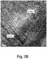
- FIG. 3A and FIG. 3Bare transmission electron microscope (TEM) images respectively illustrating a semiconductor structure and an enlarged part of the semiconductor structure according to an embodiment of the present invention
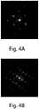
- FIG. 4A and FIG. 4Bare diagrams illustrating electron diffraction of hexagonal crystal GaN (h-GaN) and cubic crystal GaN (c-GaN) according to an embodiment of the present invention
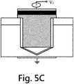
- FIGS. 5A-5Care diagrams schematically illustrating silicon-doped GaN epitaxial layers having different silicon-doped concentrations according to an embodiment of the present invention.
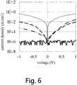
- FIG. 6is a diagram schematically illustrating results of measuring the leakage current of silicon-doped GaN epitaxial layers having different silicon-doped concentrations according to an embodiment of the present invention.
- the present inventionprovides a semiconductor structure having a Si substrate heterointegrated with GaN and a method for fabricating the same, which are suitable for the technology for high-frequency and high-power GaN/Si heterojunction transistors.
- FIGS. 1A-1Fare diagrams schematically illustrating the steps of method for fabricating a semiconductor structure having a Si substrate heterointegrated with GaN according to an embodiment of the present invention. The method comprises the following steps:
- a silicon substrate 10is provided.
- the silicon substrate 10has a main surface 11 , which has a (100) crystal surface.
- an oxide layer 20 having a given thicknessis grown on the main surface 11 of the silicon substrate 10 using thermal oxidation.
- the oxide layer 20comprises SiO 2 and has a thickness of 100 nm.
- a nanometer scale holeis patterned.
- the oxide layer 20is patterned to serve it as a hard mask using electron beam lithography.
- the silicon substrate 10is partially removed to form a hundred nanometer scale hole 30 using reactive-ion etching (RIE).
- RIEreactive-ion etching
- the hundred nanometer scale hole 30penetrates through the oxide layer 20 having a thickness of 100 nm and extends to within the silicon substrate 10 .
- the hundred nanometer scale hole 30has a depth of 250 nm within the silicon substrate 10 .
- the hundred nanometer scale hole 30has a depth of 250-700 nm within the silicon substrate 10 .
- a nitride layer 40 having a given thicknessis grown on the wall of the hundred nanometer scale hole 30 using plasma enhanced chemical vapor deposition (PECVD).
- PECVDplasma enhanced chemical vapor deposition
- the nitride layer 40comprises SiNx and has a thickness of 200 nm.
- the nitride layer 40 on the bottom wall 31 of the hundred nanometer scale hole 30is removed using inductively coupled plasma (ICP), thereby exposing the (100) crystal surface of the silicon substrate 10 and leaving the nitride layer 40 on the sidewall 32 of the hundred nanometer scale hole 30 .
- ICPinductively coupled plasma
- the nitride layer 40 on the sidewall 32is used as a blocking layer and potassium hydroxide (KOH) is used as an etching solution.
- KOHpotassium hydroxide
- the etching solutionis heated to 80° C. for 110 seconds.
- the (100) crystal surface of the silicon substrate 10 exposed from the bottom wall 31 of the hundred nanometer scale hole 30is etched at 80° C. using wet etching until a tilted surface which has the (111) crystal surface of the silicon substrate 30 is exposed, wherein the wet etching uses the KOH as the etching solution.
- the bottom wall 31 of the hundred nanometer scale hole 30 in FIG. 1Bis downward etched to have a V-like groove. Except for the V-like groove, the sidewall 32 of the hundred nanometer scale hole 30 has a depth of 200-300 nm within the silicon substrate 10 .
- an AlN buffer layer 50 and a GaN epitaxial layer 60are sequentially grown in the hundred nanometer scale hole 30 using metal organic chemical-vapor deposition (MOCVD) and silicon is doped.
- MOCVDmetal organic chemical-vapor deposition
- the doping gas of slime and hydrogenis reacted with the GaN epitaxial layer 60 to increase and control the concentration of doping silicon atoms into the GaN epitaxial layer 60 , thereby forming an ideal silicon-doped GaN epitaxial layer 60 .
- the oxide layer 20is formed on the main surface 11 of the silicon substrate 10 which has the (100) crystal surface.
- the oxide layer 20 and the silicon substrate 10are partially removed to form the hundred nanometer scale hole 30 .
- the wall of the hundred nanometer scale hole 30is formed of a sidewall 32 and a tilted surface 12 downward extended from the sidewall 32 and connected with the sidewall 32 .
- the sidewall 32is covered with the nitride layer 40 .
- the tilted surface 12has the (111) crystal surface of the silicon substrate 10 .
- the AlN buffer layer 50is formed on the tilted surface 12 of the hundred nanometer scale hole 30 .
- the silicon-doped GaN epitaxial layer 60is formed in the hundred nanometer scale hole 30 and formed on the AlN buffer layer 50 .
- the sidewall 32 of the hundred nanometer scale hole 30is roughly perpendicular to the main surface 11 of the silicon substrate 10 , which has the (100) crystal surface.
- the tilted surface 12 connected with the bottom of the sidewall 32forms a V-like groove.
- the oxide layer 20has a thickness of about 100 nm.
- the sidewall 32 of the hundred nanometer scale hole 30has a depth of about 200-300 nm within the silicon substrate 10 .
- the sidewall 32 of the hundred nanometer scale hole 30has a total depth of about 300-400 nm.
- FIG. 2is a scanning electron microscope (SEM) image illustrating a semiconductor structure according to an embodiment of the present invention.
- the silicon substrate 10has a plurality of hundred nanometer scale holes 30 .
- Each of the hundred nanometer scale holes 30 of the silicon substrate 10has a shape of a rectangle, wherein the rectangle has a width of 500 nm and a length of 5 ⁇ m.
- FIG. 3A and FIG. 3Bare transmission electron microscope (TEM) images respectively illustrating a semiconductor structure and an enlarged part of the semiconductor structure according to an embodiment of the present invention.
- the (100) silicon substrateis etched using wet etching to form the (111) crystal surface, which provides a preferred nucleating crystal surface of the AlN buffer layer and the GaN epitaxial layer.
- the hexagonal crystal GaN materials grown on the sidewallare combined with each other to form cubic crystal GaN.
- the central bottom of the hundred nanometer scale holehas a highly crystallographic defect region A 3 , and highly crystallized regions A 1 , A 2 , and A are formed from the sidewall to the surface of the silicon substrate.
- FIG. 3Bwhich is a diagram illustrating an enlarged part of the highly crystallized region A of FIG. 3A .
- hexagonal crystal GaN (h-GaN) materials being single crystalare grown on the (111) crystal surface and then combined with each other to form cubic crystal GaN (c-GaN) at the central region of the hundred nanometer scale hole.
- FIG. 4A and FIG. 4Bare diagrams illustrating electron diffraction of hexagonal crystal GaN (h-GaN) and cubic crystal GaN (c-GaN) according to an embodiment of the present invention.
- FIGS. 5A-5Care diagrams schematically illustrating silicon-doped GaN epitaxial layers having different silicon-doped concentrations according to an embodiment of the present invention.
- a black regionrepresents a highly-doped region
- an oblique-line regionrepresents lowly-doped region
- a white regionrepresents an undoped region.
- FIG. 5Ashows a highly-doped region having a thickness of 100 nm and an undoped region having a thickness of 1000 nm.
- FIG. 6is a diagram schematically illustrating results of measuring the leakage current of silicon-doped GaN epitaxial layers having different silicon-doped concentrations according to an embodiment of the present invention. The three curves from top to bottom in FIG. 6 respectively represent the results of measuring the leakage current of silicon-doped GaN epitaxial layers respectively corresponding to FIG. 5A , FIG. 5B , and FIG. 5C .
- the measured resultsshow that the high energy-gap material being GaN and the doped Si achieve low leakage current, thereby forming an ideal GaN drain, which is applied to Si-MOSFETs to solve the breakdown problem with continuing scaling down devices.
- the semiconductor structure having a Si substrate heterointegrated with GaN and the method for fabricating the same of the present inventionuse metal organic chemical-vapor deposition (MOCVD) and selective area growth (SEG) to form the GaN epitaxial layer in the hundred nanometer scale hole of the (100) silicon substrate.
- MOCVDmetal organic chemical-vapor deposition
- SEGselective area growth
- the hundred nanometer scale holeexposes the (111) crystal surface of the silicon substrate to serve as the nucleating surface.
- the lattice dislocation of the GaN epitaxial layer during a crystallization processwill end at the sidewall of the hundred nanometer scale hole.
- the hexagonal crystal GaN materialsare grown on the sidewall and then combined with each other to form cubic crystal GaN with high crystallinity at the central region of the hundred nanometer scale hole.
- the SEG techniquecan effectively control and design the size and the shape of the GaN epitaxial layer.
- the present inventionuses SEG to grow the GaN epitaxial layer and dopes Si atoms into the GaN epitaxial layer, and adjusts the ratio of doping Si atoms to control the vertical leakage current, thereby forming an ideal GaN drain.
- the wide-bandgap GaN drainis heterointegrated with Si-MOSFETs to improve the threshold voltage of the semiconductor structure, whereby the semiconductor structure features high current and high transconductance to reduce the power consumption of devices on standby, thereby applying to digital logic circuits and satisfying the requirement for applications of GaN devices in the future.
Landscapes
- Engineering & Computer Science (AREA)
- Manufacturing & Machinery (AREA)
- Microelectronics & Electronic Packaging (AREA)
- Physics & Mathematics (AREA)
- Condensed Matter Physics & Semiconductors (AREA)
- General Physics & Mathematics (AREA)
- Power Engineering (AREA)
- Computer Hardware Design (AREA)
- Chemical & Material Sciences (AREA)
- Materials Engineering (AREA)
- Crystallography & Structural Chemistry (AREA)
- Recrystallisation Techniques (AREA)
- Drying Of Semiconductors (AREA)
- Weting (AREA)
- Junction Field-Effect Transistors (AREA)
Abstract
Description
Claims (8)
Priority Applications (1)
| Application Number | Priority Date | Filing Date | Title |
|---|---|---|---|
| US17/116,585US11342179B2 (en) | 2019-05-21 | 2020-12-09 | Semiconductor structure having a Si substrate heterointegrated with GaN and method for fabricating the same |
Applications Claiming Priority (4)
| Application Number | Priority Date | Filing Date | Title |
|---|---|---|---|
| TW108117447ATWI728364B (en) | 2019-05-21 | 2019-05-21 | SEMICONDUCTOR STRUCTURE OF GaN EPITAXY IN HETEROINTEGRATION WITH Si SUBSTRATE AND METHOD OF MANUFACTURING THE SAME |
| TW108117447 | 2019-05-21 | ||
| US16/519,418US20200373153A1 (en) | 2019-05-21 | 2019-07-23 | SEMICONDUCTOR STRUCTURE HAVING A Si SUBSTRATE HETEROINTEGRATED WITH GaN AND METHOD FOR FABRICATING THE SAME |
| US17/116,585US11342179B2 (en) | 2019-05-21 | 2020-12-09 | Semiconductor structure having a Si substrate heterointegrated with GaN and method for fabricating the same |
Related Parent Applications (1)
| Application Number | Title | Priority Date | Filing Date |
|---|---|---|---|
| US16/519,418DivisionUS20200373153A1 (en) | 2019-05-21 | 2019-07-23 | SEMICONDUCTOR STRUCTURE HAVING A Si SUBSTRATE HETEROINTEGRATED WITH GaN AND METHOD FOR FABRICATING THE SAME |
Publications (2)
| Publication Number | Publication Date |
|---|---|
| US20210118670A1 US20210118670A1 (en) | 2021-04-22 |
| US11342179B2true US11342179B2 (en) | 2022-05-24 |
Family
ID=68002832
Family Applications (2)
| Application Number | Title | Priority Date | Filing Date |
|---|---|---|---|
| US16/519,418AbandonedUS20200373153A1 (en) | 2019-05-21 | 2019-07-23 | SEMICONDUCTOR STRUCTURE HAVING A Si SUBSTRATE HETEROINTEGRATED WITH GaN AND METHOD FOR FABRICATING THE SAME |
| US17/116,585Active2039-09-26US11342179B2 (en) | 2019-05-21 | 2020-12-09 | Semiconductor structure having a Si substrate heterointegrated with GaN and method for fabricating the same |
Family Applications Before (1)
| Application Number | Title | Priority Date | Filing Date |
|---|---|---|---|
| US16/519,418AbandonedUS20200373153A1 (en) | 2019-05-21 | 2019-07-23 | SEMICONDUCTOR STRUCTURE HAVING A Si SUBSTRATE HETEROINTEGRATED WITH GaN AND METHOD FOR FABRICATING THE SAME |
Country Status (4)
| Country | Link |
|---|---|
| US (2) | US20200373153A1 (en) |
| JP (1) | JP6804778B2 (en) |
| CN (1) | CN110289206A (en) |
| TW (1) | TWI728364B (en) |
Families Citing this family (5)
| Publication number | Priority date | Publication date | Assignee | Title |
|---|---|---|---|---|
| TWI715311B (en)* | 2019-11-26 | 2021-01-01 | 國立交通大學 | Si-mosfet with wide bandgap iii-v drain and method of manufacturing the same |
| CN113764433B (en)* | 2020-06-02 | 2025-02-07 | 合晶科技股份有限公司 | Semiconductor substrate and method for forming the same |
| US20230238246A1 (en)* | 2022-01-21 | 2023-07-27 | The Board Of Trustees Of The University Of Illnois | Large area synthesis of cubic phase gallium nitride on silicon |
| US20230299236A1 (en)* | 2022-03-15 | 2023-09-21 | Applied Materials, Inc. | SUBSTRATE PROCESSING FOR GaN GROWTH |
| CN116190203A (en)* | 2022-11-15 | 2023-05-30 | 湖北九峰山实验室 | Semiconductor substrate, semiconductor device and manufacturing method |
Citations (21)
| Publication number | Priority date | Publication date | Assignee | Title |
|---|---|---|---|---|
| JPH07254561A (en) | 1990-06-26 | 1995-10-03 | Texas Instr Inc <Ti> | Pattern heteroepitaxial growth method and device |
| US6245144B1 (en) | 1999-12-06 | 2001-06-12 | Lucent Technologies Inc. | Doping control in selective area growth (SAG) of InP epitaxy in the fabrication of solid state semiconductor lasers |
| JP2002110569A (en) | 2000-10-04 | 2002-04-12 | Matsushita Electric Ind Co Ltd | Semiconductor device manufacturing method, semiconductor device, and semiconductor substrate manufacturing method |
| JP2003243702A (en) | 2002-02-15 | 2003-08-29 | Nobuhiko Sawaki | Semiconductor light emitting device and method of manufacturing the same |
| TW550633B (en) | 2001-04-03 | 2003-09-01 | Mitsubishi Heavy Ind Ltd | Method for manufacturing semiconductor device |
| US6635901B2 (en) | 2000-12-15 | 2003-10-21 | Nobuhiko Sawaki | Semiconductor device including an InGaAIN layer |
| CN101300663A (en) | 2005-05-17 | 2008-11-05 | 琥珀波系统公司 | Lattice-mismatched semiconductor structures with reduced dislocation defect densities related methods for device fabrication |
| JP2009508322A (en) | 2005-06-02 | 2009-02-26 | ザ ボード オブ トラスティーズ オブ ザ ユニヴァーシティー オブ イリノイ | Printable semiconductor structure and related manufacturing and assembly methods |
| US20100072515A1 (en)* | 2008-09-19 | 2010-03-25 | Amberwave Systems Corporation | Fabrication and structures of crystalline material |
| JP2010118616A (en) | 2008-11-14 | 2010-05-27 | Seiko Epson Corp | Method of manufacturing semiconductor substrate, and semiconductor substrate |
| CN102024768A (en) | 2009-09-18 | 2011-04-20 | 台湾积体电路制造股份有限公司 | Semiconductor device and method for manufacturing semiconductor structure |
| JP2012031047A (en) | 2010-07-08 | 2012-02-16 | Ritsumeikan | Method for growing crystal and semiconductor element |
| TW201542892A (en) | 2014-01-31 | 2015-11-16 | Tokyo Electron Ltd | Gallium nitride crystal growth method and heat treatment device |
| US20160020283A1 (en) | 2014-07-15 | 2016-01-21 | International Business Machines Corporation | Hetero-integration of iii-n material on silicon |
| CN105874587A (en) | 2014-01-23 | 2016-08-17 | 英特尔公司 | III-N devices in SI trenches |
| CN106549038A (en) | 2016-12-09 | 2017-03-29 | 宁波海特创电控有限公司 | A kind of gallium nitride heterojunction HEMT of vertical stratification |
| WO2018031876A1 (en) | 2016-08-12 | 2018-02-15 | Yale University | Stacking fault-free semipolar and nonpolar gan grown on foreign substrates by eliminating the nitrogen polar facets during the growth |
| JP2018520977A (en) | 2015-06-18 | 2018-08-02 | コミサリヤ・ア・レネルジ・アトミク・エ・オ・エネルジ・アルテルナテイブ | Method for making it possible to obtain a nitride semipolar layer obtained on at least one of the following materials: gallium (Ga), indium (In) and aluminum (Al) on a crystalline substrate |
| CN108987473A (en) | 2017-05-31 | 2018-12-11 | 台湾积体电路制造股份有限公司 | Semiconductor structure and forming method thereof |
| TW201904087A (en) | 2014-09-03 | 2019-01-16 | 晶元光電股份有限公司 | Light-emitting device and manufacturing metode thereof |
| JP2019507716A (en) | 2016-02-22 | 2019-03-22 | コミッサリア ア レネルジー アトミーク エ オ ゼネルジ ザルタナテイヴ | Method for obtaining a semipolar nitride layer on a crystalline substrate |
- 2019
- 2019-05-21TWTW108117447Apatent/TWI728364B/enactive
- 2019-05-29CNCN201910456914.1Apatent/CN110289206A/enactivePending
- 2019-07-01JPJP2019123178Apatent/JP6804778B2/enactiveActive
- 2019-07-23USUS16/519,418patent/US20200373153A1/ennot_activeAbandoned
- 2020
- 2020-12-09USUS17/116,585patent/US11342179B2/enactiveActive
Patent Citations (22)
| Publication number | Priority date | Publication date | Assignee | Title |
|---|---|---|---|---|
| JPH07254561A (en) | 1990-06-26 | 1995-10-03 | Texas Instr Inc <Ti> | Pattern heteroepitaxial growth method and device |
| US6245144B1 (en) | 1999-12-06 | 2001-06-12 | Lucent Technologies Inc. | Doping control in selective area growth (SAG) of InP epitaxy in the fabrication of solid state semiconductor lasers |
| JP2002110569A (en) | 2000-10-04 | 2002-04-12 | Matsushita Electric Ind Co Ltd | Semiconductor device manufacturing method, semiconductor device, and semiconductor substrate manufacturing method |
| US6635901B2 (en) | 2000-12-15 | 2003-10-21 | Nobuhiko Sawaki | Semiconductor device including an InGaAIN layer |
| TW550633B (en) | 2001-04-03 | 2003-09-01 | Mitsubishi Heavy Ind Ltd | Method for manufacturing semiconductor device |
| JP2003243702A (en) | 2002-02-15 | 2003-08-29 | Nobuhiko Sawaki | Semiconductor light emitting device and method of manufacturing the same |
| CN101300663A (en) | 2005-05-17 | 2008-11-05 | 琥珀波系统公司 | Lattice-mismatched semiconductor structures with reduced dislocation defect densities related methods for device fabrication |
| JP2009508322A (en) | 2005-06-02 | 2009-02-26 | ザ ボード オブ トラスティーズ オブ ザ ユニヴァーシティー オブ イリノイ | Printable semiconductor structure and related manufacturing and assembly methods |
| US20100072515A1 (en)* | 2008-09-19 | 2010-03-25 | Amberwave Systems Corporation | Fabrication and structures of crystalline material |
| JP2010118616A (en) | 2008-11-14 | 2010-05-27 | Seiko Epson Corp | Method of manufacturing semiconductor substrate, and semiconductor substrate |
| CN102024768A (en) | 2009-09-18 | 2011-04-20 | 台湾积体电路制造股份有限公司 | Semiconductor device and method for manufacturing semiconductor structure |
| JP2012031047A (en) | 2010-07-08 | 2012-02-16 | Ritsumeikan | Method for growing crystal and semiconductor element |
| CN105874587A (en) | 2014-01-23 | 2016-08-17 | 英特尔公司 | III-N devices in SI trenches |
| US20170207307A1 (en) | 2014-01-23 | 2017-07-20 | Intel Corporation | Iii-n devices in si trenches |
| TW201542892A (en) | 2014-01-31 | 2015-11-16 | Tokyo Electron Ltd | Gallium nitride crystal growth method and heat treatment device |
| US20160020283A1 (en) | 2014-07-15 | 2016-01-21 | International Business Machines Corporation | Hetero-integration of iii-n material on silicon |
| TW201904087A (en) | 2014-09-03 | 2019-01-16 | 晶元光電股份有限公司 | Light-emitting device and manufacturing metode thereof |
| JP2018520977A (en) | 2015-06-18 | 2018-08-02 | コミサリヤ・ア・レネルジ・アトミク・エ・オ・エネルジ・アルテルナテイブ | Method for making it possible to obtain a nitride semipolar layer obtained on at least one of the following materials: gallium (Ga), indium (In) and aluminum (Al) on a crystalline substrate |
| JP2019507716A (en) | 2016-02-22 | 2019-03-22 | コミッサリア ア レネルジー アトミーク エ オ ゼネルジ ザルタナテイヴ | Method for obtaining a semipolar nitride layer on a crystalline substrate |
| WO2018031876A1 (en) | 2016-08-12 | 2018-02-15 | Yale University | Stacking fault-free semipolar and nonpolar gan grown on foreign substrates by eliminating the nitrogen polar facets during the growth |
| CN106549038A (en) | 2016-12-09 | 2017-03-29 | 宁波海特创电控有限公司 | A kind of gallium nitride heterojunction HEMT of vertical stratification |
| CN108987473A (en) | 2017-05-31 | 2018-12-11 | 台湾积体电路制造股份有限公司 | Semiconductor structure and forming method thereof |
Non-Patent Citations (3)
| Title |
|---|
| Chen, et al. "Growth and Fabrication of Semi-Polar InGaN/GaN Multi-Quantum Well Light-Emitting Diodes on Microstructured Si (001) Substrates." Chinese Physics B, vol. 24, No. 11 (Oct. 2015), p. 118102. doi: 10.1088/1674-1056/24/11/118102. |
| Examination Report dated Nov. 26, 2020 for corresponding CN Application No. 201910456914.1. |
| Reuters, et al. "Selective MOVPE of InGaN-Based LED Structures on Non-Planar Si (111) Facets of Patterned Si (100) Substrates." J Crystal Growth, vol. 391 (Apr. 2014). pp. 33-40. doi: 10.1016/j.jcrysgro.2014.01.002. |
Also Published As
| Publication number | Publication date |
|---|---|
| JP2020191434A (en) | 2020-11-26 |
| CN110289206A (en) | 2019-09-27 |
| JP6804778B2 (en) | 2020-12-23 |
| TWI728364B (en) | 2021-05-21 |
| TW202044494A (en) | 2020-12-01 |
| US20200373153A1 (en) | 2020-11-26 |
| US20210118670A1 (en) | 2021-04-22 |
Similar Documents
| Publication | Publication Date | Title |
|---|---|---|
| US11342179B2 (en) | Semiconductor structure having a Si substrate heterointegrated with GaN and method for fabricating the same | |
| JP5063594B2 (en) | Lattice-mismatched semiconductor structure with low dislocation defect density and related device manufacturing method | |
| US10622470B2 (en) | Process of forming nitride semiconductor device | |
| KR101255463B1 (en) | Epitaxial Substrate having Nano-rugged Surface and Fabrication thereof | |
| CN101901834B (en) | Field effect transistor and method for manufacturing the same | |
| US8203136B2 (en) | Epitaxial substrate, semiconductor light-emitting device using such epitaxial substrate and fabrication thereof | |
| CN1839466A (en) | Method of forming independent semiconductor layer | |
| US20160093492A1 (en) | Method for growing nitride-based semiconductor with high quality | |
| KR20190098715A (en) | Methods for bottom up fin structure formation | |
| US20170170313A1 (en) | Method of Producing a Pre-Patterned Structure for Growing Vertical Nanostructures | |
| TWI718934B (en) | Method of forming gallium nitride film | |
| CN106898647A (en) | Self-aligned nanostructures for semiconductor devices | |
| JP4283840B2 (en) | Method for producing group III nitride semiconductor | |
| KR102126186B1 (en) | Method for manufacturing a gallium nitride substrate | |
| EP3496131B1 (en) | Method for forming a semiconductor structure and a semiconductor structure manufactured thereof | |
| CN111952175B (en) | Method for manufacturing grooves of transistor and transistor | |
| KR101145595B1 (en) | Method for crystal growth of nitride semiconductor | |
| KR101256465B1 (en) | Nitride baced semiconductor device and manufacturing method thereof | |
| US11651958B2 (en) | Two-dimensional material device and method for manufacturing same | |
| KR101345897B1 (en) | A semiconductor device comprising a honeycomb heteroepitaxy | |
| KR20020055475A (en) | Method of fusion for heteroepitaxial layers and overgrowth thereon | |
| KR20010019358A (en) | Method for fabricating a III-nitride compound semiconductor | |
| CN119997537A (en) | A method for preparing a semiconductor structure and a semiconductor structure | |
| JP5667360B2 (en) | Semiconductor substrate, electronic device, and method for manufacturing semiconductor substrate | |
| CN120264805A (en) | An epitaxial layer of a gallium nitride HEMT device on a substrate and a manufacturing method thereof |
Legal Events
| Date | Code | Title | Description |
|---|---|---|---|
| FEPP | Fee payment procedure | Free format text:ENTITY STATUS SET TO UNDISCOUNTED (ORIGINAL EVENT CODE: BIG.); ENTITY STATUS OF PATENT OWNER: SMALL ENTITY | |
| AS | Assignment | Owner name:NATIONAL CHIAO TUNG UNIVERSITY, TAIWAN Free format text:ASSIGNMENT OF ASSIGNORS INTEREST;ASSIGNORS:CHANG, EDWARD YI;CHUANG, CHIEH-HSI;LIN, JESSIE;REEL/FRAME:054676/0082 Effective date:20201208 | |
| FEPP | Fee payment procedure | Free format text:ENTITY STATUS SET TO SMALL (ORIGINAL EVENT CODE: SMAL); ENTITY STATUS OF PATENT OWNER: SMALL ENTITY | |
| STPP | Information on status: patent application and granting procedure in general | Free format text:APPLICATION DISPATCHED FROM PREEXAM, NOT YET DOCKETED | |
| STPP | Information on status: patent application and granting procedure in general | Free format text:DOCKETED NEW CASE - READY FOR EXAMINATION | |
| STPP | Information on status: patent application and granting procedure in general | Free format text:NOTICE OF ALLOWANCE MAILED -- APPLICATION RECEIVED IN OFFICE OF PUBLICATIONS | |
| STPP | Information on status: patent application and granting procedure in general | Free format text:PUBLICATIONS -- ISSUE FEE PAYMENT RECEIVED | |
| STPP | Information on status: patent application and granting procedure in general | Free format text:PUBLICATIONS -- ISSUE FEE PAYMENT VERIFIED | |
| STCF | Information on status: patent grant | Free format text:PATENTED CASE | |
| AS | Assignment | Owner name:NATIONAL YANG MING CHIAO TUNG UNIVERSITY, TAIWAN Free format text:MERGER AND CHANGE OF NAME;ASSIGNORS:NATIONAL CHIAO TUNG UNIVERSITY;NATIONAL YANG MING CHIAO TUNG UNIVERSITY;REEL/FRAME:066371/0985 Effective date:20210201 | |
| AS | Assignment | Owner name:NATIONAL CHUNG-SHAN INSTITUTE OF SCIENCE AND TECHNOLOGY, TAIWAN Free format text:ASSIGNMENT OF ASSIGNORS INTEREST;ASSIGNOR:NATIONAL YANG MING CHIAO TUNG UNIVERSITY;REEL/FRAME:068505/0379 Effective date:20240711 Owner name:NATIONAL YANG MING CHIAO TUNG UNIVERSITY, TAIWAN Free format text:ASSIGNMENT OF ASSIGNORS INTEREST;ASSIGNOR:NATIONAL YANG MING CHIAO TUNG UNIVERSITY;REEL/FRAME:068505/0379 Effective date:20240711 | |
| FEPP | Fee payment procedure | Free format text:ENTITY STATUS SET TO UNDISCOUNTED (ORIGINAL EVENT CODE: BIG.); ENTITY STATUS OF PATENT OWNER: LARGE ENTITY | |
| MAFP | Maintenance fee payment | Free format text:PAYMENT OF MAINTENANCE FEE, 4TH YEAR, LARGE ENTITY (ORIGINAL EVENT CODE: M1551); ENTITY STATUS OF PATENT OWNER: LARGE ENTITY Year of fee payment:4 |