US11336003B2 - Multi-layer, multi-turn inductor structure for wireless transfer of power - Google Patents
Multi-layer, multi-turn inductor structure for wireless transfer of powerDownload PDFInfo
- Publication number
- US11336003B2 US11336003B2US17/150,895US202117150895AUS11336003B2US 11336003 B2US11336003 B2US 11336003B2US 202117150895 AUS202117150895 AUS 202117150895AUS 11336003 B2US11336003 B2US 11336003B2
- Authority
- US
- United States
- Prior art keywords
- layer
- conductive trace
- conductive
- antenna
- receiving antenna
- Prior art date
- Legal status (The legal status is an assumption and is not a legal conclusion. Google has not performed a legal analysis and makes no representation as to the accuracy of the status listed.)
- Active
Links
Images


Classifications
- H—ELECTRICITY
- H02—GENERATION; CONVERSION OR DISTRIBUTION OF ELECTRIC POWER
- H02J—CIRCUIT ARRANGEMENTS OR SYSTEMS FOR SUPPLYING OR DISTRIBUTING ELECTRIC POWER; SYSTEMS FOR STORING ELECTRIC ENERGY
- H02J50/00—Circuit arrangements or systems for wireless supply or distribution of electric power
- H02J50/005—Mechanical details of housing or structure aiming to accommodate the power transfer means, e.g. mechanical integration of coils, antennas or transducers into emitting or receiving devices
- A—HUMAN NECESSITIES
- A61—MEDICAL OR VETERINARY SCIENCE; HYGIENE
- A61N—ELECTROTHERAPY; MAGNETOTHERAPY; RADIATION THERAPY; ULTRASOUND THERAPY
- A61N1/00—Electrotherapy; Circuits therefor
- A61N1/02—Details
- A61N1/04—Electrodes
- A61N1/05—Electrodes for implantation or insertion into the body, e.g. heart electrode
- A61N1/0551—Spinal or peripheral nerve electrodes
- A61N1/0553—Paddle shaped electrodes, e.g. for laminotomy
- A—HUMAN NECESSITIES
- A61—MEDICAL OR VETERINARY SCIENCE; HYGIENE
- A61N—ELECTROTHERAPY; MAGNETOTHERAPY; RADIATION THERAPY; ULTRASOUND THERAPY
- A61N1/00—Electrotherapy; Circuits therefor
- A61N1/18—Applying electric currents by contact electrodes
- A61N1/32—Applying electric currents by contact electrodes alternating or intermittent currents
- A61N1/36—Applying electric currents by contact electrodes alternating or intermittent currents for stimulation
- A61N1/372—Arrangements in connection with the implantation of stimulators
- A61N1/37211—Means for communicating with stimulators
- A61N1/37217—Means for communicating with stimulators characterised by the communication link, e.g. acoustic or tactile
- A61N1/37223—Circuits for electromagnetic coupling
- A61N1/37229—Shape or location of the implanted or external antenna
- A—HUMAN NECESSITIES
- A61—MEDICAL OR VETERINARY SCIENCE; HYGIENE
- A61N—ELECTROTHERAPY; MAGNETOTHERAPY; RADIATION THERAPY; ULTRASOUND THERAPY
- A61N1/00—Electrotherapy; Circuits therefor
- A61N1/18—Applying electric currents by contact electrodes
- A61N1/32—Applying electric currents by contact electrodes alternating or intermittent currents
- A61N1/36—Applying electric currents by contact electrodes alternating or intermittent currents for stimulation
- A61N1/372—Arrangements in connection with the implantation of stimulators
- A61N1/378—Electrical supply
- A61N1/3787—Electrical supply from an external energy source
- H—ELECTRICITY
- H01—ELECTRIC ELEMENTS
- H01F—MAGNETS; INDUCTANCES; TRANSFORMERS; SELECTION OF MATERIALS FOR THEIR MAGNETIC PROPERTIES
- H01F17/00—Fixed inductances of the signal type
- H—ELECTRICITY
- H01—ELECTRIC ELEMENTS
- H01F—MAGNETS; INDUCTANCES; TRANSFORMERS; SELECTION OF MATERIALS FOR THEIR MAGNETIC PROPERTIES
- H01F17/00—Fixed inductances of the signal type
- H01F17/0006—Printed inductances
- H—ELECTRICITY
- H01—ELECTRIC ELEMENTS
- H01F—MAGNETS; INDUCTANCES; TRANSFORMERS; SELECTION OF MATERIALS FOR THEIR MAGNETIC PROPERTIES
- H01F27/00—Details of transformers or inductances, in general
- H01F27/28—Coils; Windings; Conductive connections
- H01F27/2804—Printed windings
- H—ELECTRICITY
- H01—ELECTRIC ELEMENTS
- H01F—MAGNETS; INDUCTANCES; TRANSFORMERS; SELECTION OF MATERIALS FOR THEIR MAGNETIC PROPERTIES
- H01F29/00—Variable transformers or inductances not covered by group H01F21/00
- H01F29/02—Variable transformers or inductances not covered by group H01F21/00 with tappings on coil or winding; with provision for rearrangement or interconnection of windings
- H—ELECTRICITY
- H01—ELECTRIC ELEMENTS
- H01F—MAGNETS; INDUCTANCES; TRANSFORMERS; SELECTION OF MATERIALS FOR THEIR MAGNETIC PROPERTIES
- H01F38/00—Adaptations of transformers or inductances for specific applications or functions
- H01F38/14—Inductive couplings
- H—ELECTRICITY
- H01—ELECTRIC ELEMENTS
- H01F—MAGNETS; INDUCTANCES; TRANSFORMERS; SELECTION OF MATERIALS FOR THEIR MAGNETIC PROPERTIES
- H01F41/00—Apparatus or processes specially adapted for manufacturing or assembling magnets, inductances or transformers; Apparatus or processes specially adapted for manufacturing materials characterised by their magnetic properties
- H01F41/02—Apparatus or processes specially adapted for manufacturing or assembling magnets, inductances or transformers; Apparatus or processes specially adapted for manufacturing materials characterised by their magnetic properties for manufacturing cores, coils, or magnets
- H01F41/04—Apparatus or processes specially adapted for manufacturing or assembling magnets, inductances or transformers; Apparatus or processes specially adapted for manufacturing materials characterised by their magnetic properties for manufacturing cores, coils, or magnets for manufacturing coils
- H01F41/041—Printed circuit coils
- H—ELECTRICITY
- H01—ELECTRIC ELEMENTS
- H01F—MAGNETS; INDUCTANCES; TRANSFORMERS; SELECTION OF MATERIALS FOR THEIR MAGNETIC PROPERTIES
- H01F5/00—Coils
- H—ELECTRICITY
- H01—ELECTRIC ELEMENTS
- H01F—MAGNETS; INDUCTANCES; TRANSFORMERS; SELECTION OF MATERIALS FOR THEIR MAGNETIC PROPERTIES
- H01F5/00—Coils
- H01F5/003—Printed circuit coils
- H—ELECTRICITY
- H01—ELECTRIC ELEMENTS
- H01F—MAGNETS; INDUCTANCES; TRANSFORMERS; SELECTION OF MATERIALS FOR THEIR MAGNETIC PROPERTIES
- H01F7/00—Magnets
- H01F7/06—Electromagnets; Actuators including electromagnets
- H—ELECTRICITY
- H01—ELECTRIC ELEMENTS
- H01Q—ANTENNAS, i.e. RADIO AERIALS
- H01Q1/00—Details of, or arrangements associated with, antennas
- H01Q1/36—Structural form of radiating elements, e.g. cone, spiral, umbrella; Particular materials used therewith
- H01Q1/38—Structural form of radiating elements, e.g. cone, spiral, umbrella; Particular materials used therewith formed by a conductive layer on an insulating support
- H—ELECTRICITY
- H01—ELECTRIC ELEMENTS
- H01Q—ANTENNAS, i.e. RADIO AERIALS
- H01Q7/00—Loop antennas with a substantially uniform current distribution around the loop and having a directional radiation pattern in a plane perpendicular to the plane of the loop
- H—ELECTRICITY
- H01—ELECTRIC ELEMENTS
- H01R—ELECTRICALLY-CONDUCTIVE CONNECTIONS; STRUCTURAL ASSOCIATIONS OF A PLURALITY OF MUTUALLY-INSULATED ELECTRICAL CONNECTING ELEMENTS; COUPLING DEVICES; CURRENT COLLECTORS
- H01R43/00—Apparatus or processes specially adapted for manufacturing, assembling, maintaining, or repairing of line connectors or current collectors or for joining electric conductors
- H—ELECTRICITY
- H02—GENERATION; CONVERSION OR DISTRIBUTION OF ELECTRIC POWER
- H02J—CIRCUIT ARRANGEMENTS OR SYSTEMS FOR SUPPLYING OR DISTRIBUTING ELECTRIC POWER; SYSTEMS FOR STORING ELECTRIC ENERGY
- H02J50/00—Circuit arrangements or systems for wireless supply or distribution of electric power
- H02J50/10—Circuit arrangements or systems for wireless supply or distribution of electric power using inductive coupling
- H02J50/12—Circuit arrangements or systems for wireless supply or distribution of electric power using inductive coupling of the resonant type
- H02J7/025—
- H—ELECTRICITY
- H02—GENERATION; CONVERSION OR DISTRIBUTION OF ELECTRIC POWER
- H02P—CONTROL OR REGULATION OF ELECTRIC MOTORS, ELECTRIC GENERATORS OR DYNAMO-ELECTRIC CONVERTERS; CONTROLLING TRANSFORMERS, REACTORS OR CHOKE COILS
- H02P13/00—Arrangements for controlling transformers, reactors or choke coils, for the purpose of obtaining a desired output
- H—ELECTRICITY
- H03—ELECTRONIC CIRCUITRY
- H03H—IMPEDANCE NETWORKS, e.g. RESONANT CIRCUITS; RESONATORS
- H03H7/00—Multiple-port networks comprising only passive electrical elements as network components
- H03H7/01—Frequency selective two-port networks
- H04B5/0037—
- H04B5/0062—
- H04B5/0068—
- H04B5/0075—
- H—ELECTRICITY
- H04—ELECTRIC COMMUNICATION TECHNIQUE
- H04B—TRANSMISSION
- H04B5/00—Near-field transmission systems, e.g. inductive or capacitive transmission systems
- H04B5/20—Near-field transmission systems, e.g. inductive or capacitive transmission systems characterised by the transmission technique; characterised by the transmission medium
- H04B5/24—Inductive coupling
- H—ELECTRICITY
- H04—ELECTRIC COMMUNICATION TECHNIQUE
- H04B—TRANSMISSION
- H04B5/00—Near-field transmission systems, e.g. inductive or capacitive transmission systems
- H04B5/70—Near-field transmission systems, e.g. inductive or capacitive transmission systems specially adapted for specific purposes
- H04B5/77—Near-field transmission systems, e.g. inductive or capacitive transmission systems specially adapted for specific purposes for interrogation
- H—ELECTRICITY
- H04—ELECTRIC COMMUNICATION TECHNIQUE
- H04B—TRANSMISSION
- H04B5/00—Near-field transmission systems, e.g. inductive or capacitive transmission systems
- H04B5/70—Near-field transmission systems, e.g. inductive or capacitive transmission systems specially adapted for specific purposes
- H04B5/79—Near-field transmission systems, e.g. inductive or capacitive transmission systems specially adapted for specific purposes for data transfer in combination with power transfer
- H—ELECTRICITY
- H05—ELECTRIC TECHNIQUES NOT OTHERWISE PROVIDED FOR
- H05B—ELECTRIC HEATING; ELECTRIC LIGHT SOURCES NOT OTHERWISE PROVIDED FOR; CIRCUIT ARRANGEMENTS FOR ELECTRIC LIGHT SOURCES, IN GENERAL
- H05B6/00—Heating by electric, magnetic or electromagnetic fields
- H05B6/02—Induction heating
- H05B6/06—Control, e.g. of temperature, of power
- H—ELECTRICITY
- H05—ELECTRIC TECHNIQUES NOT OTHERWISE PROVIDED FOR
- H05B—ELECTRIC HEATING; ELECTRIC LIGHT SOURCES NOT OTHERWISE PROVIDED FOR; CIRCUIT ARRANGEMENTS FOR ELECTRIC LIGHT SOURCES, IN GENERAL
- H05B6/00—Heating by electric, magnetic or electromagnetic fields
- H05B6/02—Induction heating
- H05B6/10—Induction heating apparatus, other than furnaces, for specific applications
- H05B6/12—Cooking devices
- H05B6/1209—Cooking devices induction cooking plates or the like and devices to be used in combination with them
- H05B6/1245—Cooking devices induction cooking plates or the like and devices to be used in combination with them with special coil arrangements
- H—ELECTRICITY
- H05—ELECTRIC TECHNIQUES NOT OTHERWISE PROVIDED FOR
- H05B—ELECTRIC HEATING; ELECTRIC LIGHT SOURCES NOT OTHERWISE PROVIDED FOR; CIRCUIT ARRANGEMENTS FOR ELECTRIC LIGHT SOURCES, IN GENERAL
- H05B6/00—Heating by electric, magnetic or electromagnetic fields
- H05B6/02—Induction heating
- H05B6/36—Coil arrangements
- H05B6/362—Coil arrangements with flat coil conductors
- A—HUMAN NECESSITIES
- A61—MEDICAL OR VETERINARY SCIENCE; HYGIENE
- A61N—ELECTROTHERAPY; MAGNETOTHERAPY; RADIATION THERAPY; ULTRASOUND THERAPY
- A61N1/00—Electrotherapy; Circuits therefor
- A61N1/18—Applying electric currents by contact electrodes
- A61N1/32—Applying electric currents by contact electrodes alternating or intermittent currents
- A61N1/36—Applying electric currents by contact electrodes alternating or intermittent currents for stimulation
- A61N1/3605—Implantable neurostimulators for stimulating central or peripheral nerve system
- A—HUMAN NECESSITIES
- A61—MEDICAL OR VETERINARY SCIENCE; HYGIENE
- A61N—ELECTROTHERAPY; MAGNETOTHERAPY; RADIATION THERAPY; ULTRASOUND THERAPY
- A61N1/00—Electrotherapy; Circuits therefor
- A61N1/18—Applying electric currents by contact electrodes
- A61N1/32—Applying electric currents by contact electrodes alternating or intermittent currents
- A61N1/36—Applying electric currents by contact electrodes alternating or intermittent currents for stimulation
- A61N1/372—Arrangements in connection with the implantation of stimulators
- A61N1/375—Constructional arrangements, e.g. casings
- A61N1/3756—Casings with electrodes thereon, e.g. leadless stimulators
- B—PERFORMING OPERATIONS; TRANSPORTING
- B33—ADDITIVE MANUFACTURING TECHNOLOGY
- B33Y—ADDITIVE MANUFACTURING, i.e. MANUFACTURING OF THREE-DIMENSIONAL [3-D] OBJECTS BY ADDITIVE DEPOSITION, ADDITIVE AGGLOMERATION OR ADDITIVE LAYERING, e.g. BY 3-D PRINTING, STEREOLITHOGRAPHY OR SELECTIVE LASER SINTERING
- B33Y80/00—Products made by additive manufacturing
- H—ELECTRICITY
- H01—ELECTRIC ELEMENTS
- H01F—MAGNETS; INDUCTANCES; TRANSFORMERS; SELECTION OF MATERIALS FOR THEIR MAGNETIC PROPERTIES
- H01F17/00—Fixed inductances of the signal type
- H01F17/0006—Printed inductances
- H01F17/0013—Printed inductances with stacked layers
- H—ELECTRICITY
- H01—ELECTRIC ELEMENTS
- H01F—MAGNETS; INDUCTANCES; TRANSFORMERS; SELECTION OF MATERIALS FOR THEIR MAGNETIC PROPERTIES
- H01F27/00—Details of transformers or inductances, in general
- H01F27/28—Coils; Windings; Conductive connections
- H01F27/2804—Printed windings
- H01F2027/2809—Printed windings on stacked layers
- H—ELECTRICITY
- H02—GENERATION; CONVERSION OR DISTRIBUTION OF ELECTRIC POWER
- H02J—CIRCUIT ARRANGEMENTS OR SYSTEMS FOR SUPPLYING OR DISTRIBUTING ELECTRIC POWER; SYSTEMS FOR STORING ELECTRIC ENERGY
- H02J2310/00—The network for supplying or distributing electric power characterised by its spatial reach or by the load
- H02J2310/10—The network having a local or delimited stationary reach
- H02J2310/20—The network being internal to a load
- H02J2310/23—The load being a medical device, a medical implant, or a life supporting device
- H04B5/0031—
- H—ELECTRICITY
- H04—ELECTRIC COMMUNICATION TECHNIQUE
- H04B—TRANSMISSION
- H04B5/00—Near-field transmission systems, e.g. inductive or capacitive transmission systems
- H04B5/40—Near-field transmission systems, e.g. inductive or capacitive transmission systems characterised by components specially adapted for near-field transmission
- H04B5/45—Transponders
- H—ELECTRICITY
- H05—ELECTRIC TECHNIQUES NOT OTHERWISE PROVIDED FOR
- H05K—PRINTED CIRCUITS; CASINGS OR CONSTRUCTIONAL DETAILS OF ELECTRIC APPARATUS; MANUFACTURE OF ASSEMBLAGES OF ELECTRICAL COMPONENTS
- H05K1/00—Printed circuits
- H05K1/16—Printed circuits incorporating printed electric components, e.g. printed resistor, capacitor, inductor
- H05K1/165—Printed circuits incorporating printed electric components, e.g. printed resistor, capacitor, inductor incorporating printed inductors
- H—ELECTRICITY
- H05—ELECTRIC TECHNIQUES NOT OTHERWISE PROVIDED FOR
- H05K—PRINTED CIRCUITS; CASINGS OR CONSTRUCTIONAL DETAILS OF ELECTRIC APPARATUS; MANUFACTURE OF ASSEMBLAGES OF ELECTRICAL COMPONENTS
- H05K2201/00—Indexing scheme relating to printed circuits covered by H05K1/00
- H05K2201/03—Conductive materials
- H05K2201/0332—Structure of the conductor
- H05K2201/0335—Layered conductors or foils
- H05K2201/0352—Differences between the conductors of different layers of a multilayer
- Y—GENERAL TAGGING OF NEW TECHNOLOGICAL DEVELOPMENTS; GENERAL TAGGING OF CROSS-SECTIONAL TECHNOLOGIES SPANNING OVER SEVERAL SECTIONS OF THE IPC; TECHNICAL SUBJECTS COVERED BY FORMER USPC CROSS-REFERENCE ART COLLECTIONS [XRACs] AND DIGESTS
- Y02—TECHNOLOGIES OR APPLICATIONS FOR MITIGATION OR ADAPTATION AGAINST CLIMATE CHANGE
- Y02B—CLIMATE CHANGE MITIGATION TECHNOLOGIES RELATED TO BUILDINGS, e.g. HOUSING, HOUSE APPLIANCES OR RELATED END-USER APPLICATIONS
- Y02B40/00—Technologies aiming at improving the efficiency of home appliances, e.g. induction cooking or efficient technologies for refrigerators, freezers or dish washers
- Y—GENERAL TAGGING OF NEW TECHNOLOGICAL DEVELOPMENTS; GENERAL TAGGING OF CROSS-SECTIONAL TECHNOLOGIES SPANNING OVER SEVERAL SECTIONS OF THE IPC; TECHNICAL SUBJECTS COVERED BY FORMER USPC CROSS-REFERENCE ART COLLECTIONS [XRACs] AND DIGESTS
- Y10—TECHNICAL SUBJECTS COVERED BY FORMER USPC
- Y10T—TECHNICAL SUBJECTS COVERED BY FORMER US CLASSIFICATION
- Y10T29/00—Metal working
- Y10T29/49—Method of mechanical manufacture
- Y10T29/49002—Electrical device making
- Y10T29/49005—Acoustic transducer
- Y—GENERAL TAGGING OF NEW TECHNOLOGICAL DEVELOPMENTS; GENERAL TAGGING OF CROSS-SECTIONAL TECHNOLOGIES SPANNING OVER SEVERAL SECTIONS OF THE IPC; TECHNICAL SUBJECTS COVERED BY FORMER USPC CROSS-REFERENCE ART COLLECTIONS [XRACs] AND DIGESTS
- Y10—TECHNICAL SUBJECTS COVERED BY FORMER USPC
- Y10T—TECHNICAL SUBJECTS COVERED BY FORMER US CLASSIFICATION
- Y10T29/00—Metal working
- Y10T29/49—Method of mechanical manufacture
- Y10T29/49002—Electrical device making
- Y10T29/4902—Electromagnet, transformer or inductor
- Y10T29/4908—Acoustic transducer
- Y—GENERAL TAGGING OF NEW TECHNOLOGICAL DEVELOPMENTS; GENERAL TAGGING OF CROSS-SECTIONAL TECHNOLOGIES SPANNING OVER SEVERAL SECTIONS OF THE IPC; TECHNICAL SUBJECTS COVERED BY FORMER USPC CROSS-REFERENCE ART COLLECTIONS [XRACs] AND DIGESTS
- Y10—TECHNICAL SUBJECTS COVERED BY FORMER USPC
- Y10T—TECHNICAL SUBJECTS COVERED BY FORMER US CLASSIFICATION
- Y10T29/00—Metal working
- Y10T29/49—Method of mechanical manufacture
- Y10T29/49002—Electrical device making
- Y10T29/49117—Conductor or circuit manufacturing
- Y10T29/49124—On flat or curved insulated base, e.g., printed circuit, etc.
- Y10T29/49155—Manufacturing circuit on or in base
- Y—GENERAL TAGGING OF NEW TECHNOLOGICAL DEVELOPMENTS; GENERAL TAGGING OF CROSS-SECTIONAL TECHNOLOGIES SPANNING OVER SEVERAL SECTIONS OF THE IPC; TECHNICAL SUBJECTS COVERED BY FORMER USPC CROSS-REFERENCE ART COLLECTIONS [XRACs] AND DIGESTS
- Y10—TECHNICAL SUBJECTS COVERED BY FORMER USPC
- Y10T—TECHNICAL SUBJECTS COVERED BY FORMER US CLASSIFICATION
- Y10T29/00—Metal working
- Y10T29/49—Method of mechanical manufacture
- Y10T29/49002—Electrical device making
- Y10T29/49117—Conductor or circuit manufacturing
- Y10T29/49194—Assembling elongated conductors, e.g., splicing, etc.
- Y10T29/49195—Assembling elongated conductors, e.g., splicing, etc. with end-to-end orienting
Definitions
- the present subject mattergenerally relates to methods, systems and apparatus to design, operate and manufacture wireless power and/or data transmission and/or communication systems, and more specifically, to methods, systems and apparatus to design, operate and manufacture a high efficiency structure for use in near-field wireless power and/or data transmission and/or communication systems.
- skin effectis the tendency of an alternating electric current (AC) to distribute itself within a conductor such that the current density is more predominant near the surface of the conductor with the remaining conductor body ‘unused’ relative to electrical current flow.
- the remaining conductor bodyis ‘unused’ relative to electrical current flow because the current density typically decays with distance therewithin away from the surface of the conductor.
- the electric currentflows mostly near the surface, and is referred to as the “skin” of the conductor.
- the depth at which current flows from the surfaceis referred to as the “skin depth.”
- the “skin depth”then defines the electrical signal conducting path that is active in transmission and/or communication, while the conductor is defined as the body that is capable of conducting an electrical signal.
- the skin effect phenomenongenerally causes energy loss as current flows through the antenna wire and circuit.
- Higher resistive loss at high frequenciesis a problem faced by most electronic devices or appliances. Skin effect becomes more prevalent when operating frequency increases. With higher frequencies, current that normally flows through the entire cross section of the wire forming the antenna becomes restricted to its surface. As a result, the effective resistance of the wire is similar to that of a thinner wire rather than of the actual diameter through which the current could be distributed.
- a wire exhibiting tolerable resistance for efficient performance at low frequencytransitions into a wire of unacceptable resistance at high frequency. The transition from tolerable to unacceptable resistance translates into an inefficient power and/or data transmission and/or communication system that is unable to conduct an electrical signal as needed in particular applications.
- RFIDradio frequency identification
- telemetrysensing
- communicationasset tracking
- patient monitoringdata entry and/or retrieval
- transmission misalignment limitationsare other serious problems in wireless power and/or data transmission and/or communication applications.
- IMDsImplanted Medical Devices
- pacemakersdefibrillators and neuromodulation or neuromuscular stimulation devices
- neuromuscular stimulation devicesthere is a desire to minimize battery recharge time.
- Faster battery recharge timereduces, for example, patient duration of discomfort, inconvenience, and potential for injury.
- antennashave less resistive losses, battery recharge could be accomplished from greater distances and with higher tolerance to antenna misalignment or disorientation without compromising performance. Precise orientation and alignment is known to be difficult to achieve, especially for obese patients.
- structures of smaller sizescan be designed and practically manufactured while maintaining the performance characteristics required for successful system operation, then the overall dimensions of IMD's could be decreased.
- read rangeis at most three feet which is generally insufficient for pallet tracking.
- Ultra high frequency readersenable greater read distances of eight to ten feet, however, they introduce other performance issues like signals that are reflected by metal or are absorbed by water, or display unreadable, null spots in read fields.
- Increased read rangerequires concentrated power to facilitate reflecting back the signal for better performance, hence, a more efficient structure could help solve these issues.
- Litz wireswere developed, in part, in an attempt to address the issues discussed above.
- Litz wiresare generally insufficient for use in high frequency applications, and are therefore generally not useful in applications having operating frequencies above about 3 MHz.
- a Litz wireis a wire consisting of a number of individually insulated magnet wires twisted or braided into a uniform pattern, so that each wire strand tends to take all possible positions in the cross-section of the entire conductor.
- This multi-strand configuration or Litz constructionis designed to minimize the power losses exhibited in solid conductors due to “skin effect”.
- Litz wire constructionsattempt to counteract this effect by increasing the amount of surface area without significantly increasing the size of the conductor.
- even properly constructed Litz wiresexhibit some skin effect due to the limitations of stranding.
- Wires intended for higher frequency rangesgenerally require more strands of a finer gauge size than Litz wires of equal cross-sectional area but composed of fewer and larger strands.
- the highest frequency at which providers of Litz wires offer configurations capable of improving efficienciesis about 3 MHz. There is currently no solution for applications with operating frequencies beyond this 3 MHz maximum frequency limit.
- the teachings hereinalleviate one or more of the above noted problems of higher resistive losses at high frequencies resulting in lower quality factors by utilizing a multi-layer (ML) wire structure concept to increase the area of conductance therewithin.
- the multi-layer wire configurationresults in a reduction of conductor loss and an increase in the quality factor of the structure.
- the present teachingsapply to wireless transmission and/or communication for near-field energy transfer, power transfer, data transfer or combinations thereof. More specifically, the present teachings apply to wireless transmission and/or communication for near-field antennas, energy networks, power networks or data networks, including any and all combinations of such networks.
- Wireless energy transfer or wireless power transmissionis the transmission of electrical energy from a power source to an electrical load without interconnecting wires.
- efficiencyis a significant parameter, as the transmission signal must arrive at the receiver or receivers to make the system practical.
- the most common form of wireless transmission involving energy, power, or data transferis carried out using induction followed by resonant magnetic induction.
- Other methods currently being consideredinclude electromagnetic radiation, for example but not limited to, microwaves or lasers.
- wireless energy reception or wireless power receptionis the reception of electrical energy from a power source without interconnecting wires.
- efficiencyis a significant parameter, as the reception of a signal must be received from a transmitter or transmitters to make the system practical.
- the forms of wireless reception embodying energy, power or datacan be carried out using direct induction, resonant magnetic induction as well as electromagnetic radiation in the form of microwaves or lasers.
- wireless energymay comprise harvested energy.
- harvested energymay comprise solar energy, kinetic energy, vibration based-energy harvesting, or thermal energy.
- the embodiments of the present applicationare capable of wireless communication of electrical energy, electrical power and/or data without interconnecting wires.
- Wireless communicationembodies the transmission and/or reception of electrical energy, electrical power or data either simultaneously or independently.
- the resonatormitigates the unwanted high frequency skin effect by introducing non-conducting dielectric layers within its wire, resulting in a structure that comprises layers of conducting material alternating with layers of non-conducting material.
- the structureeffectively provides an increased number of surfaces each with its characteristic skin depth and all electrically, or otherwise, connected.
- the skin depthmay range from approximately one-half of the conductor depth to about equal to the conductor depth.
- the conductor depthmay be in the range of skin depth to twice the skin depth. However, depending on the available technology, costs, and application, the conductor depth may be as large as twenty times or more the skin depth.
- the resonatormay include a coil having at least one turn wherein the coil is made up of a multi-layer wire structure.
- the multi-layer wire structuremay include a first and second conductive layer separated by a layer of insulating material.
- the conductive layersmay have substantially the same thickness and/or depth, wherein the thickness and/or depth may be in the range of skin depth to twice the skin depth. However, depending on the available technology, costs, and application, the conductor thickness and/or depth may be as large as twenty times or more the skin depth.
- Each conductive layermay be electrically connected to each other using at least one method of interconnect, such as but not limited to a via, a solder, a tab, a wire, a pin, or a rivet.
- an antenna for wireless power and/or data transfer or receptionwherein resistive losses within the antenna are minimized by maximizing useful conductor cross-sectional area in a wire cross section.
- the present applicationincorporates the multi-layer structural design within an antenna configured to transmit or receive wireless energy and/or data.
- the multi-layer structuremay be incorporated as the antenna itself or, alternatively, may be positioned within an antenna housing.
- the multi-layer structureimproves antenna transmission and reception and alleviates one or more of the above noted problems of higher resistive losses at high frequencies that result in lower antenna quality factors.
- the antenna of the present applicationmitigates the unwanted high frequency skin effect by introducing non-conducting dielectric layers within its structure, resulting in a structure that comprises layers of conducting material alternating with layers of non-conducting material.
- the antenna of the present applicationmay comprise a structure having a multi-layer-multi-turn (MLMT) design.
- MLMTmulti-layer-multi-turn
- Both the multi-layer and multi-layer-multi-turn structures of the antennaeffectively provide for an increased number of surfaces each with its characteristic skin depth and all electrically, or otherwise, connected.
- the skin depthmay be dimensioned to be about the same as or less than the conductor thickness. In an embodiment, the skin depth may range from approximately one-half of the conductor thickness to about equal to the conductor thickness.
- the antennamay comprise the shape of a coil having at least one turn wherein the coil is made up of a multi-layer wire.
- the multi-layer wiremay include a first and second conductive layer separated by a layer of insulating material.
- the conductive layersmay have substantially the same thickness and/or depth, wherein the thickness and/or depth may be in the range of skin depth to twice the skin depth.
- Each conductive layermay be electrically connected to each other using at least one method of interconnect, such as but not limited to a via, a solder, a tab, a wire, a pin, or a rivet.
- the non-conducting layer within the multi-layer structureis to insulate two different conducting layers.
- the most basic design of the non-conducting layerwould ideally be as thin as the manufacturing process practically permits, while still providing sufficient insulating properties.
- the thickness of layersis dictated by the “core thickness” and the pre-preg thickness.
- the thickness of the non-conducting layeris selected to modify the electrical behavior of the structure.
- the resonator or antennamay have a quality factor greater than 50.
- the quality factoris greater than 350.
- the quality factoris greater than 600. It will be apparent to those skilled in the art that systems requiring two resonators or two antennas may exhibit substantially similar quality factors. Also, it will be apparent to one skilled in the art that systems requiring two resonators or two antennas wherein one of the resonators or antennas may exhibit a quality factor that is substantially different than the other.
- the quality factor selection for each resonator or antennawill depend on the application, the design specification for each and the intended use of each resonator or antenna.
- the quality factor of a resonator or an antennamay be dependent on the environment in which it is used, so, for example, a resonator or an antenna that has a quality factor of 100 in air, may only have a quality factor of 50 or lower when implanted in human or animal tissue or when it is packaged in a compact hand held device within a metallic environment.
- the MLMT structure of the present application described hereinshould outperform traditional resonators or antennas.
- the reduction of losses in the wire and the significantly reduced internal resistance of the resonator or antennacould enable high efficiency, extended range, compact wireless systems that consume less energy, have longer run time and simplify operation without compromising events like overheating.
- a structure for wireless transmission or wireless receptionis designed to wirelessly transmit and/or receive electrical energy, electromagnetic energy, and/or electrical power.
- the structureis capable of electronic data transmission.
- the structureis capable of transmitting and/or receiving a combination of electrical energy, electromagnetic energy, electrical power and electronic data together or separately.
- the transmission of either or both of the electrical energy and datamay be wirelessly transmitted at about the same or different frequencies.
- electrical energymay be wirelessly transmitted at a first frequency while data may be wirelessly transmitted at a second frequency that is about the same or different than the first frequency.
- the wireless transmission of the electrical energy and electronic datamay occur simultaneously or at different times or time intervals.
- transmission or reception of the electrical energy or data by the antennamay be triggered or halted by an identification code.
- an identification codeis received by the antenna prior to wireless transmission of the electrical energy and/or data.
- the identification codeserves to provide a handshake or identification marker that helps ensure wireless transmission or reception to a specific antenna or antennas.
- the identification codemay serve to activate or deactivate an antenna.
- the identification codemay also signal that the transmission or reception of data or electrical energy is forthcoming and may provide parameters about a future transmission, such as size, duration, or time.
- the identification codemay include, but is not limited to, a data signal, an alpha numeric string, a binary code, an amount of electrical power, an electrical voltage, an electrical current or combinations thereof.
- the identification codemay be transmitted at a specific sequence, frequency, frequencies or time interval such that the identification code is a unique.
- the multi-layer structure of the resonator or antennamay comprise a plurality of conductor layers, an insulator layer separating each of the conductor layers, and at least one connector connecting two or more of the conductor layers.
- Each of the plurality of conductor layersmay have at least one turn and may further be placed in a parallel orientation.
- Each conductor layermay be formed from an electrically conductive material.
- the electrically conductive materialmay be comprised of copper, Aluminum, titanium, platinum and platinum/iridium alloys, tantalum, niobium, zirconium, hafnium, nitinol, Co—Cr—Ni alloys, stainless steel, gold, a gold alloy, palladium, carbon, silver, a noble metal or a biocompatible material and any combination thereof.
- the conductor layermay have a cross-sectional shape, such as, but not limited to, a circular cross-section, a rectangular cross-section, a square cross-section, a triangular cross-section, or an elliptical cross-section.
- the connector connecting the conductor layersmay be but is not limited to a via, a solder, a tab, a wire, a pin, or a rivet.
- the MLMT structuremay have structural shape, such as but not limited to a circular solenoidal configuration, a square solenoidal configuration, a circular spiral configuration, a square spiral configuration, a rectangular configuration, a triangular configuration, a circular spiral-solenoidal configuration, a square spiral-solenoidal configuration, and a conformal solenoid configuration.
- Other configurationsmay be used to modify the electrical properties of the structure, or to conform to the space available on a specific device
- An electrical resistance in the MLMT structuremay be reduced when an electrical signal is induced in the resonator or antenna at a frequency.
- the frequencymay be selected from a frequency range from about 100 kHz to about 10 GHz. Further, the frequency may be a frequency band that ranges from or is within about 100 kHz to about 10 GHz.
- the electrical signalmay be an electrical current, an electrical voltage, a digital data signal or any combination thereof.
- the resonator or antennamay comprise a plurality of conductors, each conductor having a conductor length, a conductor height, a conductor depth, and a conductive surface having a skin depth.
- the skin depthmay range from approximately one-half of the conductor depth to about equal to the conductor depth.
- the conductor depthmay be in the range of skin depth to twice the skin depth. However, depending on the available technology, costs, and application, the conductor depth may be as large as twenty times or more the skin depth.
- the plurality of conductor layersmay have at least one turn. Further, each of the plurality of conductor layers may or may not have substantially the same conductor length, conductor height, or conductor depth.
- the conductor layersmay be formed from an electrically conductive material.
- the electrically conductive materialmay be comprised of copper, aluminum, titanium, platinum and platinum/iridium alloys, tantalum, niobium, zirconium, hafnium, nitinol, Co—Cr—Ni alloys, stainless steel, gold, a gold alloy, palladium, carbon, silver, a noble metal or a biocompatible material and any combination thereof.
- the plurality of conductorsmay be arranged to form a resonator body.
- the resonator bodymay have a resonator body length, a resonator body width and a resonator body depth.
- the electrical signalmay be an electrical current, an electrical voltage, a digital data signal or any combination thereof.
- the plurality of conductorsmay be arranged to form an antenna body.
- the antenna bodymay have an antenna body length, an antenna body width and an antenna body depth. When an electrical signal is induced through the antenna body, the electrical signal propagates through the conducting surface of skin depth.
- the electrical signalmay be an electrical current, an electrical voltage, a digital data signal or any combination thereof.
- the plurality of conductors in the resonator or antennamay comprise a first conductor layer and a second conductor layer separated by an insulator layer wherein the first conductor layer is connected to the second conductor layer or more by at least one connector.
- the conductormay have a cross-sectional shape, such as but not limited to a circular cross-section, a rectangular cross-section, a square cross-section, a triangular cross-section, or an elliptical cross-section.
- the resonator or antennamay have a structural shape such as but not limited to a circular solenoidal, a square solenoidal configuration, a circular spiral configuration, a square spiral configuration, a rectangular configuration, a triangular configuration, a circular spiral-solenoidal configuration, a square spiral-solenoidal configuration, or a conformal solenoid configuration.
- the circuitis designed to wirelessly transmit and/or receive electrical energy, electromagnetic energy, and electrical power.
- the circuitis capable of electronic data transmission.
- the circuitis capable of transmitting a combination of electrical energy, electromagnetic energy, electrical power and electronic data together or separately.
- the circuitmay be configured to receive or prepare the identification code for transmission.
- the circuitmay activate or de-activate the antenna as well as control the operation of the antenna so that a specific amount of energy or data is transmitted or received.
- the circuitmay be used to control the frequency, time interval or sequence at which electrical energy and/or data is transmitted or received.
- Circuits at high frequenciesextensively use passive elements such as inductors, capacitors, and the like.
- Some examples of such circuit configurationsinclude but are not limited to band pass, high pass and low pass filters; mixer circuits (e.g., Gilbert Cell); oscillators such as Colpitts, Pierce, Hartley, and clap; and, amplifiers such as differential, push pull, feedback, and radio-frequency (RF).
- inductorsare used in matching and feedback in low noise amplifiers (LNAs) as a source degeneration element.
- LNAslow noise amplifiers
- Lumped inductorsare also essential elements in RF circuits and monolithic microwave integrated circuits (MMICs). Lumped inductors are used in on-chip matching networks where transmission line structures may be of excessive length.
- passive circuit element and lumped elementsuch as lumped inductor, may be used interchangeably with passive circuit element being the broader term.
- the passive circuit elementmay be an inductor, a capacitor, a resistor or just a wire. In nearly all the above mentioned circuit examples, not meant to be limiting, it is desired that the passive components are minimally lossy.
- an embodimentis given using but is not limited to an inductor.
- the designsshould be such that maximum Q is attained while achieving the desired inductance value. In other words, the resistive loss in the inductor needs to be minimized.
- the inductorcan be implemented as, but not limited to, a TEM/transmission line, a conductive loop, or a spiral/solenoid/combination structure of several shapes, for example, but not limited to, a circle, a rectangle, an ellipsoid, a square, or an irregular configuration. All these embodiments, not meant to be limiting, may be realized using the multi-layer structure in the present application.
- a resonatoras part of a larger circuit is discussed.
- a resonatoris a device or a system that exhibits resonance (i.e., oscillates) at specific frequency, frequencies, or frequency band(s), called the resonance frequency, frequencies, or frequency band(s).
- the resonance frequencyfrequencies, or frequency band(s)
- electrical circuitsthere is minimum electrical impedance at the resonance frequency, frequencies, or frequency band(s).
- the MLMT structure of the present inventionmay act as a resonator under two fundamental conditions: (1) When the MLMT structure is designed to resonate at a specific frequency, frequencies, or frequency band(s), in its environment without any additional electrical components; (2) When the MLMT structure is designed to resonate at a specific frequency, frequencies, or frequency band(s), in its environment in combination with other components (for example, but not limited to, a capacitor, a capacitor bank, a capacitor and/or an inductor network).
- the resonatormay be part of a larger circuit, and the resonance behavior may be designed to occur at a frequency, frequencies, or frequency band(s), or at a frequency, frequencies, or frequency band(s) with a certain bandwidth or certain bandwidths. Additional components (e.g., resistance) may also be added to alter the bandwidth(s).
- the systemis designed to wirelessly transmit and/or receive electrical energy, electromagnetic energy, and electrical power.
- the systemis capable of electronic data transmission.
- the systemis capable of transmitting a combination of electrical energy, electromagnetic energy, electrical power and electronic data together or separately.
- the systemmay comprise a first resonator or antenna comprising a plurality of first conductors, each first conductor having a first conductor length, a first conductor height, a first conductor depth, and a first conductive surface having a first skin depth.
- the plurality of first conductorsmay be arranged to form a first resonator body or first antenna body having a first resonator body length or first antenna length, a first resonator body width or first antenna body width and a first resonator body depth or first antenna body depth.
- the systemmay also comprise a second resonator or antenna comprising a plurality of second conductors, each second conductor having a second conductor length, a second conductor height, a second conductor depth, and a second conductive surface having a second skin depth.
- the plurality of second conductorsmay be arranged to form a second resonator body or second antenna body having a second resonator body length or second antenna body length, a second resonator body width or second antenna body width and a second resonator body depth or second antenna body depth.
- the first skin depth and the second skin depthmay be dimensioned to be less than or about equal to its respective conductor depth.
- the first skin depth and the second skin depthmay be dimensioned to be approximately one-half of the conductor depth to about equal to the conductor depth of the respective conductor depth.
- the first and second conductorsmay have at least one turn and each of the plurality of first and second conductor layers may or may not have substantially the same conductor length, conductor height, and conductor depth.
- the first conductor depth and the second conductor depthmay be dimensioned to be in the range of skin depth to twice the skin depth. However, depending on the available technology, costs, and application, the first conductor depth and the second conductor depth may be dimensioned to be as large as twenty times or more the skin depth.
- the first and second conductor layersmay be formed from an electrically conductive material such as, but not limited to, copper, Aluminum, titanium, platinum and platinum/iridium alloys, tantalum, niobium, zirconium, hafnium, nitinol, Co—Cr—Ni alloys, stainless steel, gold, a gold alloy, palladium, carbon, silver, a noble metal or a biocompatible material and any combination thereof.
- an electrically conductive materialsuch as, but not limited to, copper, Aluminum, titanium, platinum and platinum/iridium alloys, tantalum, niobium, zirconium, hafnium, nitinol, Co—Cr—Ni alloys, stainless steel, gold, a gold alloy, palladium, carbon, silver, a noble metal or a biocompatible material and any combination thereof.
- the electrical signalWhen an electrical signal is propagated through the first resonator body or first antenna body, the electrical signal propagates through the first conducting surface of skin depth and further induces an electrical signal through the second resonator body.
- the induced electrical signalpropagates through the second conducting surface at skin depth.
- the electrical signalmay be an electrical current, an electrical voltage, and a digital data signal, or combinations thereof.
- the plurality of first conductorsmay comprise a first conductor layer and a second conductor layer separated by an insulator layer wherein the first conductor layer is connected to the second conductor layer or more by at least one connector.
- the connector connecting the conductor layersmay be, but is not limited to, a via, a solder, a tab, a wire, a pin, or a rivet.
- the first conductormay have a first cross-sectional shape and the second conductor may have a second cross-sectional shape.
- the first and the second cross-sectional shapesare non-limiting and may be one of a circular cross-section, a rectangular cross-section, a square cross-section, a triangular cross-section, or an elliptical cross-section.
- the first resonator or first antennamay have a first structural shape and the second resonator or second antenna may have a second structural shape.
- the first and the second structural shapesare non-limiting and may be a circular solenoidal configuration, a square solenoidal configuration, a circular spiral configuration, a square spiral configuration, a rectangular configuration, a triangular configuration, a circular spiral-solenoidal configuration, a square spiral-solenoidal configuration, or a conformal solenoid configuration.
- a method for manufacturing a structure for wireless transmission or wireless receptioncreates the multi-layer (ML) or multi-layer-multi-turn (MLMT) structure of the present application that is capable of wirelessly transmitting and/or receiving electrical energy, electromagnetic energy, and electrical power.
- the resulting structureis capable of electronic data transmission or reception.
- the resulting structureis capable of transmitting and/or receiving a combination of electrical energy, electromagnetic energy, electrical power and electronic data together or separately.
- the methodmay comprise the steps of creating a plurality of conductor layers having an insulator between each of the conductor layers and forming at least one connection between two of the plurality of conductors.
- the connector connecting the conductor layersmay be but is not limited to a via, a solder, a tab, a wire, a pin, or a rivet.
- the conductor layersmay be created by depositing through a mask.
- the step of creating a plurality of conductor layers having an insulator between each of the conductor layersmay further include the steps of placing a first conductive layer on top of a second conductive layer and separating the first conductive layer from the second conductive layer with a first insulator.
- the step of forming at least one connection between two of the plurality of conductorsmay include the steps of connecting at least two of the conductive layers comprising but not limited to a via, a solder, a tab, a wire, a pin, or a rivet.
- the conductor layersmay be formed from an electrically conductive material.
- the electrically conductive materialmay be comprised of copper, titanium, platinum and platinum/iridium alloys, tantalum, niobium, zirconium, hafnium, nitinol, Co—Cr—Ni alloys, stainless steel, gold, a gold alloy, palladium, carbon, silver, a noble metal or a biocompatible material and any combination thereof.
- the methodcomprises the steps of providing a structure that is capable of wireless transmission and/or wireless reception of electrical energy, electromagnetic energy, and/or electrical power.
- the methodprovides the steps of providing a structure that is capable of electronic data transmission or reception.
- the methodprovides the steps of providing a structure that is capable of transmitting and/or receiving a combination of electrical energy, electromagnetic energy, electrical power and electronic data together or separately.
- the methodcomprises the steps of providing a plurality of conductors, each conductor having a conductor length, a conductor height, a conductor depth, and a conductive surface having a skin depth. Further, the method comprises the steps of providing the skin depth to range approximately one-half of the conductor depth to about equal to the conductor depth.
- the conductor depthmay be in the range of skin depth to twice the skin depth. However, depending on the available technology, costs, and application, the conductor depth may be as large as twenty times or more the skin depth.
- the plurality of conductorsmay be arranged to form a resonator body having a resonator body length, a resonator body width and a resonator body depth; and, inducing an electrical signal in at least one of the plurality of conductors such that the electrical signal propagates through the conducting surface of the skin depth.
- the electrical signalmay be an electrical current, an electrical voltage, a digital data signal or any combination thereof.
- the methodmay also include the step of providing a second plurality of conductors, each of the second conductors having a second conductor length, a second conductor height, a second conductor depth, and a second conductive surface having a second skin depth wherein the plurality of second conductors are arranged to form a second resonator body having a second resonator body length, a second resonator body width and a second resonator body depth.
- the electrical signalpropagates through the conducting surface of the skin depth and further induces an electrical signal through the second resonator body, and the induced electrical signal propagates through the second conducting surface at the second skin depth.
- the plurality of conductorsmay comprise a first conductor layer and a second conductor layer separated by an insulator layer wherein the first conductor layer is connected to the second conductor layer by at least one connector.
- the at least one connection connecting at least two of the conductive layerscomprises but is not limited to a via, a solder, a tab, a wire, a pin, or a rivet.
- the conductormay have a cross-sectional shape not limited to a circular cross-section, a rectangular cross-section, a square cross-section, a triangular cross-section, and an elliptical cross-section.
- the plurality of conductor layersmay have at least one turn and each of the plurality of conductor layers may or may not have substantially the same conductor length, conductor height, and conductor depth.
- the conductor layermay be formed from an electrically conductive material.
- the electrically conductive materialmay be comprised of copper, aluminum, titanium, platinum and platinum/iridium alloys, tantalum, niobium, zirconium, hafnium, nitinol, Co—Cr—Ni alloys, stainless steel, gold, a gold alloy, palladium, carbon, silver, a noble metal or a biocompatible material or any combination thereof.
- the resonatormay have a structural shape not limited to a circular solenoidal configuration, a square solenoidal configuration, a circular spiral configuration, a square spiral configuration, a rectangular configuration, a triangular configuration, a circular spiral-solenoidal configuration, a square spiral-solenoidal configuration, and a conformal solenoid configuration.
- FIG. 1illustrates an AC current distribution for a steady unidirectional current through a homogeneous conductor
- FIG. 2illustrates an AC current distribution at increased frequency due to skin effect
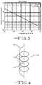
- FIG. 3is a graph of skin depth vs. frequency
- FIG. 4illustrates a high-level diagram of a structure for wireless power transfer
- FIG. 5Aillustrates an example of an antenna in a circular solenoidal configuration
- FIG. 5Billustrates an example of an antenna in a square solenoidal configuration
- FIG. 5Cillustrates an example of an antenna in a circular spiral configuration
- FIG. 5Dillustrates an example of an antenna in a square spiral configuration
- FIG. 5Eillustrates an example of an antenna in a multi-layer square spiral configuration
- FIG. 5Fillustrates an example of an antenna in a circular spiral-solenoidal configuration
- FIG. 5Gillustrates an example of an antenna in a square spiral-solenoidal configuration
- FIG. 5Hillustrates an example of an antenna in a conformal solenoid configuration
- FIG. 6Aillustrates an example of a single turn circular coil having N layers
- FIG. 6Billustrates an example of a double turn circular spiral-solenoidal coil of N layers
- FIG. 7Aillustrates an example of an antenna having a circular cross-section
- FIG. 7Billustrates an example of an antenna having a rectangular cross-section
- FIG. 7Cillustrates an example of an antenna having a square cross-section
- FIG. 7Dillustrates an example of an antenna having a triangular cross-section
- FIG. 7Eillustrates an example of an antenna having an elliptical cross-section
- FIG. 7Fillustrates a rectangular cross-section of a multi-layer wire
- FIG. 8Aillustrates a multi-layer wire having a circular cross-section
- FIG. 8Billustrates a multi-layer wire having a rectangular cross-section
- FIG. 9Ashows a single turn antenna having 1 layer
- FIG. 9Bshows an embodiment of a single turn antenna having 5 layers
- FIGS. 9C and 9Dshow embodiments of a single turn antenna having 13 layers
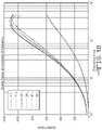
- FIG. 10is a graph illustrating the value of the quality factor as a function of frequency
- FIG. 11Ais a graph illustrating the relative changes in resistance and inductance with the number of layers
- FIG. 11Bis a graph illustrating the resultant quality factor at 10 MHz for the given number of layers
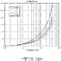
- FIG. 12Ais a graph illustrating the quality factor as a function of frequency
- FIG. 12Bis a graph illustrating the inductance relative to a 16 layer coil as a function of frequency
- FIG. 12Cis a graph illustrating the resistance relative to the 16 layer coil as a function of frequency
- FIG. 13Ais a graph illustrating the quality factor as a function of frequency
- FIG. 13Bis a graph illustrating the inductance as a function of frequency
- FIG. 13Cis a graph illustrating the resistance as a function of frequency
- FIG. 14Ais a graph illustrating the quality factor as a function of frequency for a coil having a metal strip width of 1 mm;
- FIG. 14Bis a graph illustrating the relative increase in quality factor for a coil having a metal width of 1.5 mm;
- FIG. 14Cis a graph illustrating the relative increase in quality factor for a coil having a metal width of 2 mm;
- FIG. 15illustrates a high-level block diagram of a near-field energy network
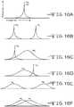
- FIG. 16Aillustrate a graph showing a situation where the receiving unit and transmitting unit have identical resonant frequencies the bands narrow;
- FIG. 16Billustrates a graph showing a situation where the receiving unit and transmitting unit have different resonant frequencies the bands narrow;
- FIG. 16Cillustrates a graph showing a situation where the receiving unit and transmitting unit have different resonant frequencies and the receiving unit has a wide resonant;
- FIG. 16Dillustrates a graph showing a situation where the receiving unit and transmitting unit have different resonant frequencies and the transmitting device is lossy;
- FIG. 16Eillustrates a graph showing a situation where the receiving unit and the transmitting unit have resonant frequencies that are far apart and both the transmitting unit and the receiving unit are lossy;
- FIG. 16Fillustrates a graph showing a situation where the receiving unit and the transmitting unit have resonant frequencies that are close and both the transmitting unit and the receiving unit are lossy;
- FIG. 17illustrates a high-level block diagram of a near-field energy network with repeaters
- FIG. 18illustrates a typical PCB stackup
- FIG. 19is a table of fabrication stack up for a 6-layer PCB board as obtained from an established PCB manufacturer
- FIG. 20illustrates an equivalent circuit diagram of any MLMT structure
- FIG. 21illustrates an equivalent circuit diagram for an MLMT structure operating as an inductor (condition 1);
- FIG. 22Aillustrates an equivalent circuit diagram for an MLMT structure operating as a self-resonator in a circuit (Type 1);
- FIG. 22Billustrates an equivalent circuit diagram for an MLMT structure operating as a stand-alone self-resonator (Type 1);
- FIG. 23Aillustrates an equivalent circuit diagram for an MLMT structure showing a capacitor addition in series
- FIG. 23Billustrates an equivalent circuit diagram for an MLMT structure showing a capacitor addition in parallel
- FIG. 24Aillustrates an equivalent circuit diagram for an MLMT structure operating as a resonator in a circuit where resonance is achieved by adding a capacitor in parallel;
- FIG. 24Billustrates an equivalent circuit diagram for an MLMT structure operating as a stand-alone resonator where resonance is achieved by adding a capacitor to the circuit in series;
- FIG. 24Cillustrates an equivalent circuit diagram for an MLMT structure operating as a stand-alone resonator where resonance is achieved by adding a capacitor to the circuit in parallel;
- the various technologies disclosed hereingenerally relate to methods, systems and apparatus to design, operate and manufacture wireless transmission and/or wireless reception systems, and more specifically, to methods, systems and apparatus to design, operate and manufacture a high efficiency structure for use in near-field wireless transmission and/or reception.
- Wireless transmissionmay embody wireless transmission of electrical energy, electromagnetic energy, and electrical power such as the embodiments.
- wireless transmissionmay embody the transmission of digital data and information.
- a combination of electrical energy, electromagnetic energy, electrical power, electronic data and informationmay be transmitted together or separately such as the embodiments discussed in energy networks. It is further contemplated that such wireless transmission could occur at the same time or over a period of time intervals.
- the electrical energy, electromagnetic energy, electrical power, and electronic datacan be wirelessly transmitted simultaneously between a transmitting structure, such as a first transmitting antenna, and a second structure, such as a second receiving antenna, at a frequency that is substantially similar or different.
- electrical energy and/or datamay be transmitted at a frequency or multiple frequencies that may range from about 10 kHz to about 10 GHz.
- wireless transmissionmay comprise near field electromagnetic coupling or far field electromagnetic coupling.
- near field electromagnetic couplingencompasses frequencies between about 10 kHz to about 50 MHz and far field electromagnetic coupling generally comprises frequencies that are greater than 50 MHz.
- far field electromagnetic couplinggenerally comprises frequencies that may range from about 50 MHz to about 10 GHz.
- Preferred far field electromagnetic coupling frequenciesinclude, but are not limited to, 6.78 MHz and 13.56 MHz, frequencies utilized in near field communication, 433 MHz, a frequency utilized in medical devices, 900 MHz and 1.8 GHz, frequencies used for cellular phone communication and 2.4 GHz, a frequency utilized by Bluetooth® and Wi-Fi communications.
- the lower frequencies of near field magnetic couplingtypically provide data transmission having a relatively low data transfer rate while the higher frequencies of far field magnetic coupling generally provide increased data transfer rates.
- wireless transmissionmay comprise in-bound or out-bound data transmission, which is also referred to as “signaling”.
- inbound data transmission or signalinginformation is transferred between a source and a target destination using about the same frequency as that used to transfer electrical energy.
- outbound data transmission or signalinginformation is transmitted at a frequency that is different than the frequency used to transmit electrical energy.
- bound signalinggenerally utilizes a frequency that is less than 50 MHz, more preferably a frequency that ranges from about 10 kHz to about 50 MHz. This is because wireless electrical power transfer generally utilizes near field magnetic coupling which typically operates at a frequency in the 10 kHz to about 50 MHz range.
- Out-bound signalingmay utilize either near field magnetic coupling or far field electromagnetic coupling.
- datais information, facts, or knowledge that may be encoded as letters and/or numbers that represent the data.
- Datamay be encoded in a variety of unlimited ways such as, but limited to, a digital or analog format, an alphanumeric string, a binary code, or an ASCII code.
- datathat is wirelessly transmitted comprises a series or sequence of electrical voltages, electrical currents or combinations thereof that is transmitted at a particular frequency or frequencies.
- datamay be transmitted by a unique sequence of electrical voltages, electrical currents, or combinations thereof that comprises an electrical signature. This transmitted electrical signature can be interpreted as data.
- the electrical signaturemay be demodulated at the receiving end by a receiving antenna or electrical circuit such that the data may be encoded into letters and/or numbers that represent the data that was wirelessly transmitted.
- Wireless receptionmay embody reception of electrical energy, electromagnetic energy, and electrical power.
- wireless receptionmay embody the reception of digital data and information.
- a combination of electrical energy, electromagnetic energy, electrical power, electronic data and informationmay be received together or received separately such as the embodiments discussed in energy networks. It is further contemplated that such wireless reception could occur at the same time or over a period of time intervals. Further embodiments of wireless reception are discussed in the energy networks, power networks, data networks and near-field power and data transfer system sections below.
- transmission of electrical energy and/or datamay be programmed to occur simultaneously or at different times or time intervals.
- the transmission of electrical energy and/or electronic datamay be programmed to occur at substantially similar or different frequencies. For example, the transmission of electrical power between a first transmitting antenna and a second receiving antenna may be specified that an amount of electrical power is transmitted at 5 GHz at 3 pm while a data signal is transmitted at 2 GHz at 3 pm and at 5 pm.
- Wireless communicationmay embody wireless transmission and reception of electrical energy, electromagnetic energy, and electrical power such as the embodiments.
- wireless communicationmay embody the transmission and reception of digital data and information.
- a combination of electrical energy, electromagnetic energy, electrical power, electronic data and informationmay be transmitted and received together or transmitted and received separately such as the embodiments discussed in energy networks. It is further contemplated that such wireless transmission and reception could occur at the same time or over a period of time intervals. Further embodiments of wireless communication are discussed in the energy networks, power networks, data networks and near-field power and data transfer system sections below.
- An antennais generally a conductor by which electromagnetic energy are sent out or received.
- An antennamay consist of, but is not limited to, a wire or a set of wires.
- a resonatoris generally any device or material that resonates, including any system that resonates.
- a resonatormay be an instrument for detecting the presence of a particular frequency by means of resonance, and may also be any circuit having this frequency characteristic. Further, a resonator may be an electrical circuit that combines capacitance and inductance in such a way that a periodic electric oscillation will reach maximum amplitude.
- antennasoften act as resonators when, for example, they self resonate or when they are coupled with another reactive element such as a capacitor to achieve resonance.
- the terms antenna and resonatorare often used interchangeably herein, and are also referred to generically as a structure (e.g., multi-layer multi-turn structure).
- “Skin effect”is generally the tendency for an alternating current to concentrate near the outer part or “skin” of a conductor. As illustrated in FIG. 1 , for a steady unidirectional current through a homogeneous conductor, the current distribution is generally uniform over the cross section; that is, the current density is the same at all points in the cross section.
- the currentWith an alternating current, the current is displaced more and more to the surface as the frequency increases. This current does not effectively utilize the full cross section of the conductor. The conductor's effective cross section is therefore reduced so the resistance and energy dissipation are increased compared with the values for a uniformly distributed current. In other words, as illustrated in FIG. 2 , due to the skin effect, the current density is maximum near the surface (also called the “skin”) of the conductor and decays exponentially to the center of the cross-section.
- the effective resistance of a wirerises significantly with frequency.
- this frequencymay range from about 100 kHz to about 3 MHz and more preferably from about 3 MHz to about 10 GHz.
- Skin depthor “penetration depth” ⁇ is frequently used in assessing the results of skin effect. It is generally accepted that the depth below the conductor surface at which the current density has decreased to about 1/e (approximately 37%) of its value at the surface. The term “skin depth” is therefore described as the depth within the cross-section where the current density has dropped to about 37% of the maximum. This concept applies to plane solids, but can be extended to other shapes provided the radius of curvature of the conductor surface is appreciably greater than ⁇ .
- the penetration depth in copperis 8.5 mm (0.33 in.); at 10 GHz it is only 6.6 ⁇ 1 ⁇ 0-7 m.
- the skin depthis a strong function of frequency and decreases with increasing frequency. This phenomenon is displayed in the graph shown in FIG. 3 .
- the fundamental concept of the multi-layer wireis to maximize the available current density over the full wire cross-section thereby reducing the wire's intrinsic resistance.
- a conductive layerwhose thickness is about twice the skin depth, it is ensured that the current density at all points in the wire is greater than or equal to ⁇ 37% of the maximum possible current density (at surface).
- a different base current densitywill be obtained. For example, by using a layer thickness of about 4 times the skin depth, it will be ensured that current density is greater than or equal to ⁇ 14% of the maximum possible current density (at surface). Similarly, for conductor depth approximately 6 times the skin depth, the current density is greater than or equal to 5%.
- an ideal proposed configuration for a multilayer wireincludes conductive layers with thickness/depth about twice the skin depth, and an insulating layer, as thin as technologically possible.
- the skin depthwhich is the conductive area active in wireless communication, ranges from approximately one-half of the conductor depth to about equal to the conductor depth.
- designing MLMT structuresmay also result in embodiments wherein the conductor depth, which is the area capable of conducting a signal but not necessarily fully utilized as operating frequencies increase, ranges from skin depth to about twice the skin depth.
- Wave-guide and resonant cavity internal surfaces for use at microwave frequenciesare therefore frequently plated with a high-conductivity material, such as silver, to reduce the energy losses since nearly all the current is concentrated at the surface.
- a high-conductivity materialsuch as silver
- the conductoris as good as a solid conductor of the coating material.
- “Quality factor”is generally accepted as an index (figure of measure) that measures the efficiency of an apparatus like an antenna, a circuit, or a resonator. Via is defined herein as an electrically conductive connection from one layer to another.
- a Litz wireis generally a wire constructed of individual film insulated wires bunched or braided together in a uniform pattern of twists and length of lay.
- FIG. 4illustrates a high-level diagram of a resonator for wireless power and/or data transfer, such as an antenna.
- the resonatorincludes a coil 100 and a multi-layer wire 101 .
- the shape of the coil 100may be circular, rectangular, triangular, some other polygon, or conformal to fit within a constrained volume.
- FIG. 4illustrates one exemplary configuration of a coil in the form of a circular shaped coil 100 .
- the configuration of the coil 100may be solenoidal, spiral, or spiral-solenoid.
- a solenoid coilfollows a helical curve that may have multiple turns where each turn has the same radius.
- a spiral coil configurationmay have a number of turns with a progressively increasing or decreasing radius.
- a spiral-solenoidal coil configurationis a combination of a spiral and solenoidal configuration. Other configurations known to those of ordinary skill may also be utilized to form the coil.
- FIGS. 5A-5Hillustrate examples of different antenna configurations that may be utilized.
- FIG. 5Aillustrates an example of an antenna in a circular solenoidal configuration 102 .
- FIG. 5Billustrates an example of an antenna in a square solenoidal configuration 103 .
- FIG. 5Cillustrates an example of an antenna in a circular spiral configuration 104 .
- FIG. 5Dillustrates an example of an antenna in a square spiral configuration 105 . It is understood that other spiral configurations, such as rectangular or triangular shape may also be utilized.
- FIG. 5Eillustrates an example of an antenna in a multi-layer square spiral configuration 106 . It should be noted that although only two layers are illustrated in FIG. 5E , it is understood that any number of layers may be used.
- the multiple layersmay be connected using but not limited to vias, solder, tabs, wires, pins, or rivets.
- the plurality of conductor layers less than or equal to the total number of layersmay be connected electrically in parallel.
- the plurality of conductor layers connected electrically in parallelmay be connected electrically in series with one or more of a plurality of conductor layers connected electrically in parallel.
- These connectorsserve at least the following two purposes: (1) the connectors connect the layers of wire for the multi-layer wire; and (2) the connectors connect one turn of the multi-layer wire to a second turn of the multi-layer wire. For example, a two-turn antenna then, there would be at least one via from the first turn to the second turn. Other purposes may also be served by the connectors.
- Viascan be of the form commonly used in printed circuit board (PCB) technologies (for example, through-hole, buried, blind) or those utilized in semiconductor or MEMS technology.
- the viacan be, but is not limited to, any conductive material that is laser-welded, welded, printed, soldered, brazed, sputtered deposited, wire-bonded and the like in order to electrically connect at least any two layers and/or all layers.
- FIG. 5Fillustrates an example of an antenna in a circular spiral-solenoidal configuration 107 .
- FIG. 5Gillustrates an example of an antenna in a square spiral-solenoidal configuration 108 .
- FIG. 5Hillustrates an example of an antenna in a conformal solenoid configuration 109 .
- the antenna in a conformal configurationmay take the form of but is not limited to a circular or rectangular solenoid or a circular or rectangular spiral. Any of the antenna configurations shown in FIGS. 5A-5H may be used with the present system.
- the coil 100 of FIG. 4may have a plurality of turns 110 .
- a turnmay be but is not limited to a bend, fold or an arc in the wire until the wire completes a revolution around the central axis point of the coil 111 .
- a turnmay be in the same or similar shape of the coil configuration, such as, for example, but not limited to a circle, a rectangle, a triangle, some other polygonal shape, or conformal to fit within a constrained volume.
- FIG. 6Aillustrates a single turn circular coil having N layers, where “N” is a number equal to or greater than one.
- FIG. 6Billustrates a double turn circular solenoidal coil of N layers.
- the inductanceincreases as T x
- the resistanceincreases as T y
- Tis the number of turns.
- x and yare 2 and 1 respectively.
- FIG. 13three performance examples are given.
- the graphcompares a 32 Layer-2 Turn antenna with a 32 Layer-1 Turn antenna and a 64 Layer-1 Turn antenna.
- the inductance and resistance for the 32 Layer-2 Turn antennaincrease between 3-3.5 times and 1.7-3 times, respectively; over the 32 Layer-1 Turn antenna in the frequency range 1 MHz-200 MHz. This increase is very near expected values from simplistic analytical relations wherein resistance is approximately T; and inductance is approximately T 2 .
- the multi-layer wire 101 in FIG. 4may have but is not limited to a circular, rectangular, square, or triangular cross-sectional shape. In addition, other shapes known to those of ordinary skill may also be utilized.
- FIGS. 7A-7Eillustrate examples of cross-sections of wires that may be used in the design of an antenna.
- FIG. 7Aillustrates an example of an antenna having a circular cross-section 401 .
- FIG. 7Billustrates an example of an antenna having a rectangular cross-section 402 .
- FIG. 7Cillustrates an example of an antenna having a square cross-section 403 .
- FIG. 7Dillustrates an example of an antenna having a triangular cross-section 404 .
- FIG. 7Eillustrates an example of an antenna having an elliptical cross-section 405 .
- FIG. 7Fillustrates a rectangular cross-section of a multi-layer wire having a first conductive layer 410 and a second conductive layer 420 .
- the multi-layer wire 101may be comprised of a rigid wire structure, a fixed flexible wire structure or a combination thereof.
- An insulating material 430separates the first layer 410 from the second layer 420 .
- the first layer 410 and second layer 420are connected with vias 440 which traverse the insulating material 430 .
- the conductive layers 410 , 420may be layers of conductive tape/ribbon/sheet/leaf or deposited metal having a metal thickness and metal strip width.
- the metal thickness of the first layer 410is identified by line A-A and the metal strip width of the first layer 410 is identified by line B-B.
- the metal thickness of a layermay be approximately twice the skin depth. The skin depth may range from approximately one-half of the conductor depth to about equal to the conductor depth Each layer in a turn will have substantially the same metal thickness and metal strip width.
- the thickness of the insulating materialmay be sufficient to meet the needs of the application or equal to the minimum thickness possible by the available fabrication technology. Additionally, the overall structure feasibility depends on the frequency of operation (as shown in the graph of FIG. 10 ), associated costs and fabrication technology utilized. Generally in PCB technology, the thickness of layers is dictated by the “core thickness” and the pre-preg thickness. In other designs, the thickness of the non-conducting layer is selected to modify the electrical behavior of a structure.
- Typical PCB stackupcomprises alternating layers of the core and the pre-preg.
- the coregenerally comprises a thin piece of dielectric with copper foil bonded on both sides.
- the core dielectricis generally cured fiberglass-epoxy resin.
- the pre-pregis generally uncured fiberglass-epoxy resin.
- the pre-pregwill cure (i.e., harden) when heated and pressed.
- the outermost layersare generally pre-preg with copper foil bonded to the outside (surface foils).
- Stackupis generally symmetric about the center of the board in the vertical axis to avoid mechanical stress in the board under thermal cycling as shown in FIG. 18 .
- the conductor and insulating layer thicknessesare equal to the minimum thickness possible by the available fabrication technology is given for an application at 13.56 MHz.
- the skin depthis about 17.8 micrometers.
- the conductor depthshould be about 35.6 micrometers and the insulation thickness should be as small as possible.
- the fabrication stack up obtained for a 6-layer PCB boardis about 71 micrometers which is nearly 4 times the skin depth.
- the insulating layeris more than 3 times the conductive layer. Advanced PCB techniques, which come at a significantly higher cost, may allow a lower conductor and insulation depth.
- PCB techniques currently in the research stagecould allow the conductive material like copper as low as 5 micrometers and the insulating dielectric about 39 micrometers.
- Other techniquessuch as semiconductor fabrication and MEMS fabrication techniques could allow much thinner layer thickness leading to performance that is nearer to ideal. If semiconductor or MEMS fabrication is used, the thicknesses of both the conducting layers and the insulating layers may be as thin as a few 100 nanometers or even thinner. In a preferred embodiment, the dielectric layer thickness is less than 200 micrometers and as perfectly insulating as possible, and with a permittivity lower than 10.
- the dielectric layercould be made from several materials, and can be of various configurations. For example, some applications may require extremely low parasitic capacitance. In such cases, a non-conducting dielectric with the lowest possible permittivity is preferred. Additionally, it may be desired to increase the insulating layer thickness to minimize the parasitic effects. Another example would be for applications that might require ferrite materials to increase inductance and/or increase magnetic shielding. In such cases, the dielectric layers might be replaced by a ferrite film/block or similar propertied configuration/material.
- the insulating materialwill be of a thickness such that the thickness is within the practical capabilities of the manufacturing technology used to manufacture that resonator and compatible with the efficiency needs of the application for which the resonator is intended.
- the material of the conductive layersmay be copper or gold, however, other materials are possible. To enhance conductivity, copper or gold with a layer of deposited silver may also be used.
- the typically known biocompatible materialsshould be utilized, including additions for enhancing conductivity. These may include, but are not limited to, conductive material taken from the group of: titanium, platinum and platinum/iridium alloys, tantalum, niobium, zirconium, hafnium, nitinol, Co—Cr—Ni alloys such as MP35N, Havar®, Elgiloy®, stainless steel, gold and its various alloys, palladium, carbon, or any other noble metal.
- the insulating materialmay be (i) air, (ii) a dielectric with a low permittivity (such as, for example, Styrofoam, silicon dioxide, or any suitable biocompatible ceramic), (iii) a non-conductive dielectric with a high permittivity, (iv) a ferrite material, or (v) a combination of the materials listed above.
- a dielectric with a low permittivitysuch as, for example, Styrofoam, silicon dioxide, or any suitable biocompatible ceramic
- a non-conductive dielectric with a high permittivitysuch as, for example, Styrofoam, silicon dioxide, or any suitable biocompatible ceramic
- a non-conductive dielectric with a high permittivitysuch as, for example, Styrofoam, silicon dioxide, or any suitable biocompatible ceramic
- a non-conductive dielectric with a high permittivitysuch as, for example, Styrofoam, silicon dioxide, or any suitable biocompatible ceramic
- a high capacitive effectis required to affect a lower self-resonance frequency of an antenna
- a high permittivity dielectricmight be preferred, or, a combination of materials including a ferrite film or ferrite block might be preferred to increase the self-inductance of the antenna.
- the use of a ferrite coremay be used to provide increased performance.
- FIG. 8A - FIG. 8Billustrate examples of different multi-layer wire cross-sectional configurations.
- FIG. 8Aillustrates a multi-layer wire having a circular cross-section 510 .
- FIG. 8Billustrates a multi-layer wire having a rectangular cross-section 520 .
- the via 530 that connects the conductive layers 540is positioned at the port or input 550 , which is the beginning of the wire.
- the positioning of the vias 530 that connect the conductive layersmay impact the performance of the antenna. For example, insufficient vias may lead to phase differences between the different layers. Conversely, an abundance of vias may lead to additional cyclical current paths that may increase the resistive loss.
- the viasmay be located at the beginning of the wire (e.g., port, input, etc.), or at one or more locations along the wire. Additionally, the vias between one set of two or more conductive layers may be at a different location than another set of two or more conductive layers. It is understood that several variations may be possible depending on the application and the system design.
- the viacan be made using techniques standard to the technology being utilized for the fabrication of the multi-layer multi-turn structure. In other cases, the vias can be implemented using soldering techniques, such as, by connecting the several layers at via locations using electric solder, welded tabs, laser weld tacking, or other commonly known electrical connecting techniques.
- the antennais preferably designed with a high quality factor (QF) to achieve efficient transfer of power that reduces intrinsic resistive losses of the antenna at high frequencies.
- the quality factoris the ratio of energy stored by a device to the energy lost by the device.
- the QF of an antennais the rate of energy loss relative to the stored energy of the antenna.
- a source device carrying a time-varying current, such as an antennapossesses energy which may be divided into three components: 1) resistive energy (W res ), 2) radiative energy (W rad ), and 3) reactive energy (W rea ).
- W resresistive energy
- W radradiative energy
- W reareactive energy
- near-field communicationsradiative and resistive energies are released by the device, in this case the antenna, to the surrounding environment.
- energymust be transferred between devices having limited power stores, e.g., battery powered devices having size constraints, excessive power loss may significantly reduce the devices' performance effectiveness.
- near-field communication devicesare designed to minimize both resistive and radiative energies while maximizing reactive energy. In other words, near-field communications benefit from maximizing Q.
- the efficiency of energy and/or data transfer between devices in an inductively coupled systemis based on the quality factor of the antenna in the transmitter (Q1), the quality factor of the antenna in the receiver (Q2), and the coupling coefficient between the two antennas ( ⁇ ).
- the efficiency of the energy transfervaries according to the following relationship: eff ⁇ ⁇ 2 ⁇ Q 1 Q 2 .
- a higher quality factorindicates a lower rate of energy loss relative to the stored energy of the antenna.
- a lower quality factorindicates a higher rate of energy loss relative to the stored energy of the antenna.
- the coupling coefficient ( ⁇ )expresses the degree of coupling that exists between two antennas.
- the quality factor of an inductive antennavaries according to the following relationship:
- Q2 ⁇ ⁇ ⁇ ⁇ fL R
- fthe frequency of operation
- Lthe inductance
- Rthe total resistance (ohmic+radiative).
- a higher quality factormay be achieved using multiple layers in a multi-layer wire for a single turn of coil. Increasing the number of turns in a coil may also be used to increase the quality factor of the structure. For a design at a constant frequency, there may be an optimum number of layers to reach a maximum quality factor. Once this maxima is reached, the quality factor may decrease as more layers are added.
- the design variables that may be used for the multi-layer multi-turn structureinclude:
- the antennamay be a single turn circular coil having multi-layer wire, as illustrated in FIGS. 9A-9D .
- the single turn coilincludes a single turn and may include a metal strip width of approximately 1.75 mm, a metal thickness of approximately 0.03 mm, an insulating layer of approximately 0.015 mm, and an outer radius of approximately 5 mm.
- the wiremay have between 5 and 60 layers, such as 5, 11, 20, 26, 41, or 60 layers.
- FIG. 9Ashows a single turn antenna having 1 layer
- FIG. 9Bshows a single turn antenna having 5 layers
- FIGS. 9C and 9Dshow embodiments of a single turn antenna having 13 layers. Although specific examples are shown in FIGS.
- the wiremay have less than 5 or more than 60 layers in order to achieve a high quality factor.
- the corresponding coil thickness for the range of 5 to 60 layersmay be between approximately 0.2 mm to 3 mm, such as for example, 0.2, 0.5, 1, 1.25, 2.05, or 3 mm, respectively.
- the quality factor at 10 MHzis approximately 80.
- the quality factoris increased to approximately 210.
- an increase in the number of layers per turnresults in an increase in quality factor until maxima is reached, after which the quality factor starts to decrease. This decrease may occur when the total height of the antenna becomes comparable to its radius.
- the degradationstarts due to greatly increased parasitic effects due to the multiple layers (e.g. capacitance and proximity effects).
- increasing the layers to 20, 26, 41 and 60results in quality factors of approximately 212, 220, 218 and 188, respectively.
- FIG. 10provides a graph of the value of the quality factor as a function of frequency.
- FIG. 11Ais a graph illustrating the relative changes in resistance and inductance with the number of layers.
- FIG. 11Billustrates the resultant quality factor at 10 MHz.
- the data points on the graphcorrespond as data point 1 is for 1 layer, data point 2 is for 11 layers, data point 3 is for 20 layers, data point 4 is for 26 layers, data point 5 is for 41 layers, and data point 6 is for 60 layers.
- These two viasare preferably located at the ports of the wire/structure.
- optimal performance for 10 MHzis achieved for an antenna configuration having 26 layers and 1 turn.
- the peak quality factoris obtained around 35 MHz and is approximately 1100.
- the antennamay be a single turn circular coil of multi-layer wire and may have a metal strip width of approximately 1 mm, a metal thickness of approximately 0.01 mm, an insulating layer of approximately 0.005 mm, and an outer radius of approximately 5 mm.
- the wiremay have between 16 and 128 layers, such as 16, 32, 64, or 128 layers. However it is understood that the wire may have less than 16 or more than 128 layers in order to achieve a high quality factor.
- the corresponding coil thickness for the range of 16 to 128 layersmay be between approximately 0.25 mm to 2 mm, such as for example, 0.25, 0.5, 1, or 2 mm, respectively.
- the quality factorimproves with increasing the number of layers, with larger quality factors achieved at higher frequencies.
- the quality factor for 16, 32, 64 and 128 layersis approximately 127, 135, 140 and 185, respectively.
- the peak quality factorincreases to nearly 2900 at approximately 450 MHz under these design parameters.
- the relative resistancemay be lowest around the frequency at which the conductor thickness is about twice the skin depth. In this example, that frequency is 160 MHz.
- FIGS. 12A-Care graphs illustrating the performance parameters and trends.
- FIG. 12Ais a graph illustrating the quality factor as a function of frequency.
- FIG. 12Bis a graph illustrating the inductance relative to a 16 layer coil as a function of frequency.
- FIG. 12Cis a graph illustrating the resistance relative to the 16 layer coil as a function of frequency.
- the quality factorimproves with an increasing number of layers with relatively larger quality factors at higher frequencies.
- FIGS. 12B-Cwhere it is shown that where the inductance is relatively constant (as compared to a 16 layer 1 turn coil) with frequency, while the resistance decreases as frequency increases as shown by the troughs around 100 MHz in FIG. 12C .
- the peak quality factorgoes up to approximately 2900 at around 450 MHz.
- FIGS. 13A-Care graphs illustrating the performance parameters and trends for this 32 layer, double turn antenna compared to the 32 and 64 layer, single turn antennas in the preceding example.
- FIG. 13Ais a graph illustrating the quality factor as a function of frequency.
- FIG. 13Bis a graph illustrating the inductance as a function of frequency.
- 13Cis a graph illustrating the resistance as a function of frequency.
- the inductanceis nearly constant and the resistance follows trends similar to the single turn antennas.
- both the inductance and resistancerise rapidly due to the contribution of parasitic capacitance, which is explained below.
- an antennamay display parasitic effects. Associated with the antenna is a parasitic capacitance that is frequency dependent and whose contribution to the overall impedance increases with frequency. As a result of the parasitic capacitance, there exists a self-resonance frequency for the antenna beyond which the antenna behaves like a capacitor. To prevent the onset of parasitic capacitance, the antenna may be designed such that the inductance is nearly unchanging around the frequency of operation. Preferably, the slope of the reactance versus frequency graph is nearly linear (around the frequency of operation) with slope, ⁇ X/ ⁇ ⁇ L (where X is the reactance, and L is the inductance that was designed for). Operating the antenna in this regime ensures that the parasitic coupling via electric fields is kept to a minimum. It is understood that that the X versus ⁇ may not be perfectly linear due to other effects such as current crowding, proximity and skin effects.
- the coilmay include a metal strip width of approximately 1 mm, a metal thickness of approximately 0.01 mm, an insulating layer of approximately 0.01 mm, and an outer radius of approximately 10 mm.
- Increasing the width of the metalreduces the resistance and the inductance, resulting in a higher quality factor. Due to the overall large size of the antenna (outer radius ⁇ 10 mm), the relatively small increase in the width (w) does not reduce the inductance.
- FIGS. 14A-Care graphs illustrating the quality factors as a function of frequency for this example with a metal strip width of approximately 1 mm, 1.5 mm and 2 mm, respectively.
- the quality factor at 379 MHzis approximately 1425 for a metal strip width of 1 mm.
- Increasing the metal strip width to 1.5 mm and 2 mmincreases the quality factor to approximately 1560 and 1486, respectively.
- utilization of near-field communication for wireless transmission and/or receptioncan be applied to energy, power or data networks.
- FIG. 15illustrates a high-level block diagram of a near-field energy network 10 .
- the network 10includes a plurality of devices 11 a-d (generally referred to as device 11 ). Each device 11 may include a transceiver.
- the transceivermay include a transmitting unit 12 a-d and a receiving unit 14 a-d for wireless communications. Although each transceiver may include a transmitting unit 12 and a receiving unit 14 , it is understood that the transceiver may comprise only a transmitting unit 12 or only a receiving unit 14 .
- the transmitting unit 12 and the receiving unit 14 in the transceivermay share certain or all circuit elements or may have separate and distinct circuit elements. Further, the transmitting unit 12 and/or receiving unit 14 may be coupled to a load 16 .
- the load 16may comprise of components within the device 11 , outside the device 11 , or a combination of components within and outside the device 11 .
- Each transmitting unit 12includes a transmitting antenna 13 .
- the transmitting antenna 13has a resonant frequency w and preferably has minimal resistive and radiative losses.
- the load 16may include driver circuitry to generate signals to drive the transmitting antenna 13 . Based on the received signals, the transmitting antenna 13 may produce a near-field in all directions (omni-directional) or may produce a near-field targeted towards a specific direction (directional).
- the targeted near-fieldmay be produced through shielding, such as by ferrite materials. Of course, it is understood to those skilled in the art that other materials may be used to provide targeted near-fields.
- Each receiving unit 14includes a receiving antenna 15 .
- a single antennamay be used for both the receiving antenna 15 and the transmitting antenna 13 or a separate antenna may be used for the receiving antenna 15 and the transmitting antenna 13 .
- Each antenna 13 , 15has a resonant frequency (referred to as ⁇ a - ⁇ d ). If separate transmitting and receiving antenna are used, it is preferred that the resonant frequency of the receiving antenna 15 is equal to the resonant frequency of the transmitting antenna 13 .
- a receiving unit 14 of one device 11e.g., receiving unit 14 b of device 11 b
- the transmitting unit 12 of another device 11e.g., transmitting unit 12 a of device 11 a
- an electromagnetic field generated by the transmitting unit 12 awill interact with the receiving unit 14 b .
- the reactive electromagnetic fields of the transmitting unit 11 awill induce an alternating current within the receiving unit 14 b .
- the induced currentmay be used to provide power or convey data to load 16 b .
- device 11 bis able to absorb energy from device 11 a .
- any number of devices having a resonant frequency equal to the resonating frequency of the transmitting devicemay be added to the near-field energy network and draw energy from the transmitting device, provided that the resonant frequency of the transmitting unit 12 a is not significantly altered due to the loading effect of the added devices.
- the receiving unit 14e.g., receiving unit 14 c of device 11 c having resonant frequency ⁇ c
- the transmitting unit 12e.g., transmitting unit 12 a of device 11 a having resonant frequency ⁇ a
- the receiving unit 14 cwill have a high impedance to the transmitting unit 12 a and will draw little energy from the transmitting unit 12 a .
- FIGS. 16A-Fillustrates graphs showing how various factors affect the transfer of energy.
- FIG. 16Aillustrates a situation where ⁇ a and ⁇ c are identical and the bands narrow. This represents an ideal scenario and the case of maximum power transfer efficiency.
- FIG. 16Billustrates a situation where ⁇ a and ⁇ c are different and the bands narrow. No energy is transferred in this scenario.
- FIG. 16Cillustrates a situation where ⁇ a and ⁇ c are different and receiving unit 14 c has a wide resonant. A wider resonant band occurs when an antenna has higher resistive and radiative losses.
- Receiving unit 14 chas more impedance to ⁇ a than in the situation shown in FIG. 16B , but is still able to absorb some energy from transmitting device 11 a .
- FIG. 16Aillustrates a situation where ⁇ a and ⁇ c are identical and the bands narrow. This represents an ideal scenario and the case of maximum power transfer efficiency.
- FIG. 16Billustrates a situation where ⁇ a and ⁇ c are different and the bands narrow. No energy
- FIG. 16Dillustrates a situation where ⁇ a and ⁇ c are different and transmitting device 11 a is lossy. Resistive and radiative losses in transmitting device 11 a lead to a wide resonant band. A smaller portion of the antennas energy is available for transfer to receiving unit 14 c .
- FIG. 16Eillustrates a situation where ⁇ a and ⁇ c are far apart and both the transmitting unit 12 a and the receiving unit 14 c are lossy. Here, no energy is transferred from the transmitting unit 12 a to the receiving unit 14 c .
- FIG. 16Fillustrates a situation where ⁇ a and ⁇ c are close and both the transmitting unit 12 a and the receiving unit 14 c are lossy. Energy is transferred between the transmitting unit 12 a and the receiving unit 14 c but the system is inefficient due to high losses.
- a power transfer networkmay be developed according to the present teachings. As illustrated in FIG. 17 , when a receiving unit 14 b is placed within the near-field of a transmitting unit 12 a and the resonant frequency of the receiving unit 14 b (i.e., ⁇ b ) is approximately equal to the resonant frequency of the transmitting unit 12 a ( ⁇ a ), energy will transfer from the transmitting unit 12 a to the receiving unit 14 b .
- each receiving devicee.g., 11 b - 11 d
- the receiving devices 11 a - 11 dmay include a transducer which may use the induced alternating current to store energy in a power storage device, such as battery or capacitor. Alternatively, the transducer may use induced alternating current to directly power electronic components within or couple to the receiving device (e.g., 11 b - 11 d ).
- one or more repeaters 18may be used in order to deliver energy to receiving devices 11 outside of the near-field (e.g., receiving unit 11 e ).
- the one or more repeaters 18may contain an antenna 20 which is tuned to ⁇ a .
- the repeater 18may draw energy from the transmitting unit 12 via the antenna 20 in the form of an induced current.
- the one or more repeaters 18may use the induced current to produce a second energy field using the antenna 20 .
- the second energy fieldmay be produced using a second antenna (not shown).
- the second energy fieldmay be used to induce an alternating current in the receiving unit 14 e .
- the receiving unit 14 emay include a transducer which may use the induced alternating current to store energy in a power storage device, such as battery or capacitor. Alternatively, the transducer may use induced alternating current to power electronic components within the receiving unit 14 e .
- the antenna 20 or second antennamay produce a near-field in all directions (omni-directional) or may produce a near-field targeted towards a specific direction (directional).
- a data transfer networkmay be developed according to the present teachings.
- a network or system designed for data transferwould be similar to the power networks described previously, except that the signal transmitted by the transmitting devices in the network may be modulated time-varying signals which carry data.
- One example of a data network layoutincludes one or more receiving units ( 14 b-d ) placed within the near-field of a transmitting unit 12 a .
- Each of the receiving units ( 14 b-d )may be capable of communicating to the transmitting unit 12 a and/or other receiving units 14 . It is understood that receiving units which may be out of near-field of the transmitting unit 12 may be reached using one or more repeaters 18 in the manner described above.
- a receiving unit 14may be placed far-field of the transmitting unit 12 and utilize the radiative field of the transmitting unit 12 for communication. Such far-field communication is achieved in a manner similar to far-field communication techniques known to those of ordinary skill in the art.
- the devices 11 within the networksmay be designed to handle data-transfer in several ways.
- the devices 11 and their antennas 13 , 15may be designed to (1) receive data only; (2) transmit data only; or (3) receive and transmit data, using either a shared antenna for receiving and transmitting or separate and dedicated antennas for receiving and transmitting.
- the devices 11may be designed to handle both data- and power-transfer.
- each device 11may be designed to: (1) transfer data only; (2) transfer power only; (3) transfer data and power, where each device 11 may use any combination of sending/receiving data and sending/receiving power, each device 11 has a shared antenna for data- and power-transfer, or each device 11 has separate, dedicated antennas for data- and power-transfer.
- Each transmitting unit 12 and/or receiving unit 14may have an identification code (ID) that is unique to the transmitting or receiving unit 12 , 14 or, alternatively, the transmitting or receiving antenna 13 , 15 .
- IDacts as an identifier for a particular transmitting or receiving unit 12 , 14 or antenna 13 , 15 on the network or system and allows for the receiving unit or antenna 14 , 15 to identify the other transmitting unit or antenna 12 , 13 for communication therebetween.
- the identification code (ID)may enable or disable transmission of electrical energy and/or data between the transmitting and receiving units or antennas 12 , 14 , 13 , 15 .
- Examples of electronic identifiers or identification codesmay include, but are not limited to, a data string, an alpha numeric string, an ASCII string, a binary code, an amount of electrical energy, an electrical voltage, an electrical current, or combinations thereof transmitted in a specific sequence, frequency and/or frequencies for a specific length of time and/or time interval(s).
- the electronic identifier or identification codeis a unique sequence of electrical voltages and/or electrical currents.
- the identification codeserves to provide a handshake or identification marker that helps ensure wireless transmission or reception to a specific antenna or antennas 13 , 15 .
- the identification codemay serve to activate or deactivate an antenna 13 , 15 .
- the identification codemay also signal that the transmission or reception of data or electrical energy is forthcoming and may provide parameters about a future transmission, such as size, duration, or time.
- the electronic identifiermay comprise an alpha numeric string transmitted at a specific frequency and/or at a specific time or time interval.
- the unique identifier (ID)may comprise a specific sequence or combinations of electrical energy and/or data.
- the transmitter and/or the receivermay not transmit or receive data and/or electrical energy until a specific identification code is transmitted or received.
- a transmitting devicesuch as an antenna
- a receiving devicewould identify a receiving device with its ID and begin communications using an initiation instruction.
- the data transfercould occur using a specified modulation scheme.
- Security protocolssuch as various encryption protocols may also be used to ensure that the data transferred by and stored in the devices are secure and not accessible to unauthorized devices which are not present in the designed network 10 .
- a circuitmay be electrically connected to either or both of the transmitting and receiving antennas 13 , 15 .
- the circuitmay be configured to receive or transmit the identification code.
- the circuitmay prepare the identification code prior to transmission by the antenna.
- the circuitmay activate or de-activate the antenna 13 , 15 as well as control the operation of the antenna so that a specific amount of energy or data is transmitted or received.
- the circuitmay be used to control the frequency, time interval or sequence at which electrical energy and/or data is transmitted or received.
- Periodic data communicationmay occur between a transmitting unit 12 and one or more receiving units 14 or between a receiving unit 14 and one or more other receiving units 14 .
- a transmitting unit 12may identify a particular receiving unit 14 based on its ID and initiate a communication session.
- a receiving unit 14may identify a transmitting unit 12 based on its ID and initiate a communication session. The communication session may be terminated by either the transmitting unit 12 or the receiving unit 14 .
- two receiving units 14may connect directly with each other in direct communication.
- two receiving units 14 or antennasmay connect with each other using the transmitting unit 12 as an intermediary.
- each receiving unit 14may connect to the transmitting unit 12 and the transmitting unit 12 would receive information from one receiving unit 14 and transmit it to the other receiving unit 14 .
- two receiving units 14may communicate using one or more repeaters 18 where the one or more repeaters 18 may receive a signal from a receiving unit 14 and transmit it to another receiving unit 14 .
- the one or more repeaters 18may be one or more stand-alone resonant antennae and may be independent of any circuitry.
- the system and method illustrated in FIG. 15 and FIG. 17 to efficiently transfer energy between two or more devicesmay be used in a variety of applications in order to operate household appliances such as vacuums, irons, televisions, computer peripheral devices; mobile devices; military applications such as surveillance equipment, night vision devices, sensor nodes and devices; transportation applications such as sensors designed to monitor automobile or train performance and safety; aerospace applications, such as control of flaps, rudders, or landing gear; space technology; naval applications such as applications to power unmanned watercraft; traffic control applications such as road imbedded sensors; industrial applications; asset tracking such as RFID tags and transponders; robotic networks; and medical devices.
- household appliancessuch as vacuums, irons, televisions, computer peripheral devices; mobile devices; military applications such as surveillance equipment, night vision devices, sensor nodes and devices; transportation applications such as sensors designed to monitor automobile or train performance and safety; aerospace applications, such as control of flaps, rudders, or landing gear; space technology; naval applications such as applications to power unmanned watercraft; traffic control applications such as road imbedded sensors; industrial applications
- near-field power and data transferare derived from the same physical principles. When utilized together, near-field power and data transfer provide an opportunity to create a wide variety of systems. The following describes a general system for near-field power and data transfer.
- a near field power and data networkmay consist of multiple transmitting and receiving units.
- NF-PDATnear field power and data network
- a simpler networkconsisting of a single transmitting unit 12 and a single receiving unit 14 is considered. The following description follows the path of the energy as it is transferred from the transmitting unit 12 to the receiving unit 14 and to a load coupled to the receiving unit 14 .
- the primary sourcemay be a main 50/60 Hz wall socket, a standard battery, a rechargeable battery connectable to a wall socket, or a rechargeable battery with indirect recharging.
- a wall-socketis one preferred method of obtaining energy because of its abundance in this form.
- batteriesmay be used.
- rechargeable batteriesmay be used. Rechargeable batteries may be replenished when their stored energy falls below a capacity. It is known that recharging allows batteries to be sued in devices that would otherwise drain batteries too quickly, have too little space for batteries of an appropriate size, or have limited access for replacing the battery.
- a primary source of powersuch as a wall socket or another battery may be used to replenish battery life in the rechargeable battery.
- rechargingis typically accomplished by connecting the battery to a wall socket for a short period of time (e.g., laptops and cell-phones).
- a wall socketfor a short period of time (e.g., laptops and cell-phones).
- direct attachment to a power cordis not possible.
- indirect recharging methodssuch as inductive coupling to an external power source, have been used. It is understood that recharging may be accomplished by other methods. For example, if there exists a clear line-of-sight between the energy source and the device, an optical link, laser, or highly-directive radio-frequency beam may be used to transfer energy.
- Alternative sources of energymay be used to power the system or to provide energy for components within the system (such as recharging a battery). These may include the conversion of one form of energy into electrical energy.
- One such exampleis the conversion of kinetic energy into electrical energy. This may be accomplished by converting movement into energy.
- a device attached to the bodymay use body movements to spin a rotor that causes a generator to produce an alternating current.
- Another exampleis the conversion of light energy into electrical energy.
- photovoltaic cells placed externallymay convert sunlight or ambient room light into energy.
- changes in pressuremay be converted into electrical energy.
- a piezoelectric appropriately placed on a devicemay be used to convert pressure changes (e.g. air pressure changes or direct pressure through contact) into electrical currents.
- thermal gradientsmay be converted into electrical energy.
- a thermo-electric generatorplaced within a device may be used to convert a temperature gradient across the device into electrical energy.
- TEGthermo-electric generator
- Such a TEGmay be useful in devices that produce heat during their operation, as a portion of the heat energy could be converted into electrical energy.
- the present teachingsalso include a method for designing a multi-layer multi-turn antenna for use in a high efficiency wireless power and data telemetry system. Given a certain frequency of operation, one or more of the following steps may be followed to design application-specific antennae:
- the present teachingsalso include a method of manufacturing the antenna after the antenna is designed.
- the multi-layer multi-turn antennautilizes strips of metal that may be deposited through a specific mask in, for example but not limited to, a PCB/ceramic/metal printing process or in a semiconductor foundry.
- An alternative method of fabricating the antennamay utilize conductive tape/ribbon/sheet/leaf with one or more tape/ribbon/sheet/leaf placed on top of each other separated by an insulating layer and shorting the multiple strips by soldering at the designated via locations.
- Another method of fabricating the antennawould be to cut out specific shapes from conductive sheets or “leaf” (e.g., gold or copper leaf) and following steps that similar to that for the conductive tape/ribbon.
- a three dimensional printing processmay also be used in addition to metal deposition processes like physical vapor deposition, thin film deposition, thick film deposition and the like.
- the present teachingslend themselves to be incorporated with current fabrication techniques for multi-layer printed wiring board, printed circuit boards and semiconductor fabrication technologies with multi-layer interconnects. As advancements in fabrication techniques are made, it is expected that the multi-layer multi-turn antenna will likely benefit greatly from such improvements. This compatibility with conventional fabrication techniques will allow these antennas to be relatively easily incorporated into conventional circuit boards. Such advances may also provide accurate repeatability and small feature sizes (i.e., high resolution).
- the design and structure of the present systemallows for extended range (i.e., the separation distance between a transmitting and a receiving wireless antenna).
- the increase in rangeenables power to be transferred across a greater distance, allowing the transmitter to be further away from the receiver.
- the tag read range for high frequency interrogatorsis no greater than 3 feet, which is insufficient for certain applications, such as pallet tracking.
- the wireless antenna of the present systemoffers an improvement for pallet tracking via RFID by delivering the concentrated power that this particular application requires to facilitate reflecting the interrogator signal needed for better extended read range performance.
- the extended range provided by the present inventionenables transfer of power to devices in difficult to reach locations, or to devices in harsh environments. In consumer electronics the extended range allows for the user to charge or transfer energy to a device from a more convenient location.
- the present systemalso enables multiple operational needs from a single design concept, namely, the multi-layer multi-turn antenna.
- the present systemmay serve as a receiver antenna, a source antenna, a transceiver (acting as a source and a receiver), and as a repeater antenna.
- the designmay be used for inductor designs solely as a lumped element in a circuit (e.g., in RF filters circuits, RF matching circuits).
- the MLMT antenna structure of the present inventionmay be represented in various circuit design embodiments.
- An equivalent circuit diagram for the MLMT antenna structureis given in FIG. 20 . It comprises the following parameters:
- the characteristics of the MLMT antenna embodimentdepend on the design values of L M , R M , and C M ; the operating center frequency and additional components that are placed across Terminal 1 and Terminal 2.
- Z ⁇ ⁇ 11 j . ⁇ . C M Equation ⁇ ⁇ 1 ⁇ ( a )
- Z ⁇ ⁇ 2R M + j . ⁇ . L M Equation ⁇ ⁇ 1 ⁇ ( b )
- Z inputZ ⁇ ⁇ 1.
- the MLMT antenna structure of the present inventionthen can be represented in various circuit design embodiments.
- the MLMT antenna structurecan be operated in three modes:
- the unique arrangement of the layers and customized wire segmentation in the present system compared with existing design technologiesdemonstrates improved system performance in similar and smaller packaging volumes as shown by quality factors that are more than 2 times higher than those realized from existing technologies.
- the present systempermits pairing of the inductance and quality factor with a specific application to optimally achieve a desired response, including, but not limited to, wireless tissue stimulation, wireless telemetry, wireless component recharging, wireless non-destructive testing, wireless sensing, and wireless energy or power management.
- Another specific advantage of the present systemis that it enables a more efficient means of Near Field Magnetic Coupling (NFMC) for power and/or data transfer in an equivalent or smaller design volume by reducing conductor loss associated with increasing frequencies (due to the phenomenon referred to as Skin Effect).
- NFMCNear Field Magnetic Coupling
- the proposed systemalso provides a solution that can be relatively easily achieved by existing manufacturing techniques (for example multi-layer printed wiring board), and can therefore be integrated with other circuit components such as ICs, resistors, capacitors, surface mount components, etc.
- Other advantages of the present systemincludes reducing power consumption thereby leading to longer battery lives (where applicable), a reduction in the Joule heating of the antenna, decreasing the consumption of environmental resources of the appliance/device, and any other benefit derived from a more energy efficient device.
Landscapes
- Engineering & Computer Science (AREA)
- Power Engineering (AREA)
- Health & Medical Sciences (AREA)
- Physics & Mathematics (AREA)
- Electromagnetism (AREA)
- Computer Networks & Wireless Communication (AREA)
- Manufacturing & Machinery (AREA)
- Animal Behavior & Ethology (AREA)
- Veterinary Medicine (AREA)
- Public Health (AREA)
- General Health & Medical Sciences (AREA)
- Life Sciences & Earth Sciences (AREA)
- Biomedical Technology (AREA)
- Nuclear Medicine, Radiotherapy & Molecular Imaging (AREA)
- Radiology & Medical Imaging (AREA)
- Signal Processing (AREA)
- Microelectronics & Electronic Packaging (AREA)
- Heart & Thoracic Surgery (AREA)
- Cardiology (AREA)
- Orthopedic Medicine & Surgery (AREA)
- Neurosurgery (AREA)
- Acoustics & Sound (AREA)
- Neurology (AREA)
- Near-Field Transmission Systems (AREA)
Abstract
Description
- It is preferred that there be at least 2 connectors connecting all of the layers that form a single conductor. These two connectors will ideally be at the two ends of the multilayer wire (the input and the output of the multilayer wire)
- It is preferred the total number of connectors should be chosen commensurate with the needs of a particular application. More than the optimum number of connectors will increase current paths which can lead to increased capacitance, increased resistance, reduced quality factor and higher bandwidth. It should also be noted that parasitic effects can become more pronounced when the overall length (height, depth) of the connector is greater than the optimum at a specific operating frequency. The length of the connector in essence is the height of the connector, and this should be kept smaller than about the (effective wavelength)/20, though keeping it within wavelength/10 could also lead to a workable embodiment, depending on the application. The reason for these restrictions is that the increased connector lengths will introduce significant phase differences between the different layers of the multilayer wire being used. These phase differences between the different layers will introduce unwanted capacitive effects, which will effectively lower self-resonance frequencies and increase losses. It should be mentioned that, for embodiments in which no additional components (for e.g. capacitors) are utilized and the structure is being used as a self-resonant resonator, connectors such as but not limited to vias with depth higher than (effective wavelength)/10 might be incorporated in the design of the antenna.
where f is the frequency of operation, L is the inductance, and R is the total resistance (ohmic+radiative). As QF is inversely proportional to the resistance, a higher resistance translates into a lower quality factor.
- a. Metal strip width, wn(e.g. w1: width of the 1stconductive layer, wk: width of the kthconductive layer). Also referred to as metal width or strip width
- b. Number of conductive layers per turn, Nn(e.g. number of layers in 1stturn, N1)
- c. Thickness of each conductive layer, dn(e.g. d1: thickness of 1stlayer, dk: thickness of kthlayer)
- d. Thickness of insulation, din(e.g. di1: thickness of insulation under 1stlayer, dik: thickness of insulation under kthlayer)
- e. Number of turns, T
- f. Number of vias connecting the different conductive layers in each turn
- g. Location of vias connecting the different conductive layers in each turn
- h. Shape (circular, rectangular, some polygon; depends on the application; for e.g. could be conformal to fit just outside or just inside some device or component)
- i. Configuration: solenoidal, spiral, spiral-solenoidal, etc.)
- j. Dimensions (length, width, inner radius, outer radius, diagonal, etc.)
| TABLE 1 | |||
| Antenna Configuration-1 | Inductance | Resistance | Quality Factor |
| Using above formula | IE3D (numerical) | Lformula | Lnumerical | Rformula | Rnumerical | Qformula | Qnumerical |
| 1 turn | 1- | 30 nH | 28.7 nH | 0.0583 | 0.0337 | 1225 | 2034 |
| R = 1 cms | R = 1 cms | ||||||
| A (wire radius) = 1 mm | Strip width ~1 mm | ||||||
| Wire area ~3.14 mm2 | Layer thick. ~0.01 mm | ||||||
| f = 380 MHz | Total thick. ~2.5 mm | ||||||
| Total wire area ~2.5 mm2 | |||||||
| MLMT design | |||||||
| 1 turn | 1- | 30 nH | 9 nH | 0.0583 | 0.0083 | 1225 | 2671 |
| R = 1 cms | R = 0.5 cms | ||||||
| A (wire radius) = 1 mm | Strip width ~1 mm | ||||||
| Wire area ~3.14 mm2 | Layer thick. ~0.01 mm | ||||||
| f = 380 MHz | Total thick. ~2 mm | ||||||
| Total wire area ~2 mm2 | |||||||
| MLMT design | |||||||
| TABLE 2 | |||
| Antenna Configuration-2 | Inductance | Resistance | Quality Factor |
| Using above formula | IE3D (numerical) | Lformula | Lnumerical | Rformula | Rnumerical | Qformula | Qnumerical |
| 1 | 1 turn | 830 | nH | 1.16 μH | 0.0815 | 0.0498 | 1161 | 2489 |
| R = 15 cms | R = 15 cms | |||||||
| (wire radius) = 2 mm | Strip width ~2 mm | |||||||
| Wire area ~12.5 mm2 | Layer thick ~0.03 mm | |||||||
| f = 17 MHz | Total Thick ~1 mm | |||||||
| Total wire area ~2 mm2 | ||||||||
| MLMT design | ||||||||
| 1 | 1 turn | 1.92 | μH | 2.48 μH | 0.1854 | <0.08 | 1105 | >2500 |
| R = 30 cms | R = 30 cms | |||||||
| (wire radius) = 2 mm | Strip width ~3 mm | |||||||
| Wire area ~12.5 mm2 | Layer thick ~0.03 mm | |||||||
| f = 17 MHz | Total Thick ~1 mm | |||||||
| Total wire area ~3 mm2 | ||||||||
| MLMT design | ||||||||
- 1. Perform analytical calculations and system level simulations to obtain minimum required inductance for sufficient coupling coefficient
- 2. Based on analytical calculations (e.g., for coupling coefficient, induced voltage, etc.), choose the number of turns required for the appropriate inductance
- 3. Select the conductor layer thickness to be about 2 times the skin depth or the minimum allowable based on the fabrication technology; whichever is higher.
- 4. Select the insulation thickness to be the minimum allowable by the fabrication technology or a larger thickness to achieve desired performance.
- 5. Select the maximum surface area possible (depends on the application). This area need not necessarily be square or circular. It could be any shape conforming to the overall system and could meander around other components.
- 6. Select the maximum number of layers possible depending on fabrication technology and the application.
- 7. Design a multi-layer multi-turn antenna in a numerical modeling tool (e.g., based on MoM or FDTD or FEM or MLFMM OR some other or combination of these) with the number of turns from step-1 and 2, and optimize (Steps 3-6) the number of layers and other parameters.
- a. Ensure that the Quality factor peak is obtained in the whereabouts of the selected frequency
- b. Ensure that the inductance for this quality factor is greater than or equal to the minimum allowable (from system level constraints)
- c. If required, ensure that the E-fields are minimized by keeping the parasitic capacitive effects low (refer to previous section)
- LM=Intrinsic Inductance
- CM=Intrinsic Capacitance
- RM=Intrinsic Resistance
- Mode 1: as an inductor such as embodied in a lumped circuit element, when
condition 1, which is given by equation 2(a), is satisfied resulting in equation 2(b). The equivalent circuit diagram is given inFIG. 21 .
Z1>>Z2 Equation 2(a)
Zinput≈Z2 Equation 2(b) - Mode 2: as a resonator such as embodied in a stand-alone tank circuit or embodied in an HF and/or RF circuit, where the resonator may be one of two types
- Type 1: as a self-resonator, when
condition 2, given byequation 3 is satisfied. The equivalent circuit diagrams are given inFIGS. 22A and 22B
ω2.LM.CM≈1Equation 3 - Type 2: as a resonator, where resonance is achieved by adding a capacitor, CADDED, in series or parallel. The equivalent circuit diagrams showing series and parallel capacitor additions are given in
FIGS. 23A and 23B . TheMode 2Type 2 circuit diagrams are given inFIGS. 24A, 24B, and 24C . - In both
Type 1 andType 2, LPickupand Lfeedrefer to a pickup inductor and a feed inductor, respectively. These are coils which have an inductance that is smaller than the inductance value of the MLMT structure, LM, and have a certain coupling to the MLMT structure. The coupling may be varied to achieve the desirable matching conditions for power transfer to or from the MLMT structure from or to the rest of the system. For simplicity and proof of concept, the embodiments described herein provide a single capacitor, CADDEDexample for achieving resonance for illustration purposes. In a practical circuit, a more complex circuit comprising multiple capacitors and/or inductors and/or resistors may be used. All embodiments shown inFIGS. 22 and 24 may be used on the transmitter side and/or on the receiver side of the system.
- Type 1: as a self-resonator, when
- Mode 3: as a capacitor, when
condition 3, given byequation 4 is satisfied
(Condition 3)
ω2.LM.CM>1Equation 4
- Mode 1: as an inductor such as embodied in a lumped circuit element, when
Claims (30)
Priority Applications (1)
| Application Number | Priority Date | Filing Date | Title |
|---|---|---|---|
| US17/150,895US11336003B2 (en) | 2009-03-09 | 2021-01-15 | Multi-layer, multi-turn inductor structure for wireless transfer of power |
Applications Claiming Priority (6)
| Application Number | Priority Date | Filing Date | Title |
|---|---|---|---|
| US15868809P | 2009-03-09 | 2009-03-09 | |
| PCT/US2010/000714WO2010104569A1 (en) | 2009-03-09 | 2010-03-09 | System and method for wireless power transfer in implantable medical devices |
| US13/233,686US8567048B2 (en) | 2009-03-09 | 2011-09-15 | Method of manufacture of multi-layer wire structure |
| US14/059,100US9444213B2 (en) | 2009-03-09 | 2013-10-21 | Method for manufacture of multi-layer wire structure for high efficiency wireless communication |
| US15/227,192US11476566B2 (en) | 2009-03-09 | 2016-08-03 | Multi-layer-multi-turn structure for high efficiency wireless communication |
| US17/150,895US11336003B2 (en) | 2009-03-09 | 2021-01-15 | Multi-layer, multi-turn inductor structure for wireless transfer of power |
Related Parent Applications (1)
| Application Number | Title | Priority Date | Filing Date |
|---|---|---|---|
| US15/227,192ContinuationUS11476566B2 (en) | 2009-03-09 | 2016-08-03 | Multi-layer-multi-turn structure for high efficiency wireless communication |
Publications (2)
| Publication Number | Publication Date |
|---|---|
| US20210135348A1 US20210135348A1 (en) | 2021-05-06 |
| US11336003B2true US11336003B2 (en) | 2022-05-17 |
Family
ID=80856665
Family Applications (5)
| Application Number | Title | Priority Date | Filing Date |
|---|---|---|---|
| US15/227,192ActiveUS11476566B2 (en) | 2009-03-09 | 2016-08-03 | Multi-layer-multi-turn structure for high efficiency wireless communication |
| US16/706,407ActiveUS11335999B2 (en) | 2009-03-09 | 2019-12-06 | Device having a multi-layer-multi-turn antenna with frequency |
| US17/150,895ActiveUS11336003B2 (en) | 2009-03-09 | 2021-01-15 | Multi-layer, multi-turn inductor structure for wireless transfer of power |
| US17/966,542ActiveUS11916400B2 (en) | 2009-03-09 | 2022-10-14 | Multi-layer-multi-turn structure for high efficiency wireless communication |
| US18/587,546ActiveUS12316128B2 (en) | 2009-03-09 | 2024-02-26 | Multi-layer-multi-turn structure for high efficiency wireless communication |
Family Applications Before (2)
| Application Number | Title | Priority Date | Filing Date |
|---|---|---|---|
| US15/227,192ActiveUS11476566B2 (en) | 2009-03-09 | 2016-08-03 | Multi-layer-multi-turn structure for high efficiency wireless communication |
| US16/706,407ActiveUS11335999B2 (en) | 2009-03-09 | 2019-12-06 | Device having a multi-layer-multi-turn antenna with frequency |
Family Applications After (2)
| Application Number | Title | Priority Date | Filing Date |
|---|---|---|---|
| US17/966,542ActiveUS11916400B2 (en) | 2009-03-09 | 2022-10-14 | Multi-layer-multi-turn structure for high efficiency wireless communication |
| US18/587,546ActiveUS12316128B2 (en) | 2009-03-09 | 2024-02-26 | Multi-layer-multi-turn structure for high efficiency wireless communication |
Country Status (1)
| Country | Link |
|---|---|
| US (5) | US11476566B2 (en) |
Families Citing this family (11)
| Publication number | Priority date | Publication date | Assignee | Title |
|---|---|---|---|---|
| FR3073662B1 (en)* | 2017-11-14 | 2022-01-21 | Arjo Wiggins Fine Papers Ltd | MULTILAYER INDUCTOR |
| CN110018356A (en)* | 2019-01-19 | 2019-07-16 | 四川大学 | Wireless and passive probe |
| US11101848B2 (en)* | 2020-01-03 | 2021-08-24 | Nucurrent, Inc. | Wireless power transmission system utilizing multiple transmission antennas with common electronics |
| KR102804836B1 (en)* | 2020-02-04 | 2025-05-09 | 쓰리엠 이노베이티브 프로퍼티즈 캄파니 | A coil assembly and method of terminaitng a coil to a circuit board |
| US20210337635A1 (en)* | 2020-04-23 | 2021-10-28 | Powermat Technologies Ltd. | Heating coil design for wireless power systems |
| US11482888B2 (en)* | 2020-06-19 | 2022-10-25 | Medtronic, Inc. | Antenna for use with RF energy harvesting |
| TWI794795B (en)* | 2021-04-26 | 2023-03-01 | 國立陽明交通大學 | Inductive resonant wireless charging system, resonant wireless charging transmitting device, wireless charging relay device and inductive wireless charging receiving device |
| CN112992524B (en)* | 2021-05-19 | 2021-07-27 | 广东电网有限责任公司东莞供电局 | A transformer wire welding device |
| US12142932B2 (en)* | 2021-11-03 | 2024-11-12 | Electronics And Telecommunications Research Institute | Wireless power transmission resonator using conducting wire with vertical rectangular cross-section |
| US20230226362A1 (en)* | 2022-01-19 | 2023-07-20 | Pacesetter, Inc. | Method of producing an implantable medical device |
| KR102658992B1 (en)* | 2023-08-24 | 2024-04-19 | 주식회사 에너지마이닝 | Self-Care Capable Smart Band for Wound and Smart Band control system including the same |
Citations (281)
| Publication number | Priority date | Publication date | Assignee | Title |
|---|---|---|---|---|
| US2797393A (en) | 1951-03-07 | 1957-06-25 | Bell Telephone Labor Inc | Composite wave guide |
| US2911605A (en) | 1956-10-02 | 1959-11-03 | Monroe Calculating Machine | Printed circuitry |
| US3141144A (en)* | 1961-02-10 | 1964-07-14 | Scanwell Lab Inc | Printed circuit delay line |
| US3231894A (en)* | 1960-06-23 | 1966-01-25 | Sony Corp | Zigzag antenna |
| US3413716A (en)* | 1965-04-30 | 1968-12-03 | Xerox Corp | Thin-film inductor elements |
| US3436687A (en)* | 1966-12-27 | 1969-04-01 | Honeywell Inc | Printed circuit delay line having mutually opposed,spiralled,inductance elements |
| US3484731A (en) | 1967-10-05 | 1969-12-16 | Edward L Rich | Printed circuit inductor |
| US4328531A (en) | 1979-03-30 | 1982-05-04 | Hitachi, Ltd. | Thick film multilayer substrate |
| US4494100A (en) | 1982-07-12 | 1985-01-15 | Motorola, Inc. | Planar inductors |
| US4578654A (en)* | 1983-11-16 | 1986-03-25 | Minnesota Mining And Manufacturing Company | Distributed capacitance lc resonant circuit |
| EP0310396A1 (en) | 1987-09-29 | 1989-04-05 | Kabushiki Kaisha Toshiba | Planar inductor |
| JPH01310518A (en) | 1988-06-09 | 1989-12-14 | Toshiba Corp | planar inductor |
| US4918418A (en)* | 1988-08-04 | 1990-04-17 | Caterpillar Inc. | Inductive coil structure with electrical return path |
| US4996165A (en) | 1989-04-21 | 1991-02-26 | Rockwell International Corporation | Self-aligned dielectric assisted planarization process |
| US5137478A (en) | 1991-04-01 | 1992-08-11 | National Standard Parts, Inc. | Sealed solder wire connector assembly and method of use |
| JPH0583249A (en) | 1991-03-29 | 1993-04-02 | Toshiba Corp | Isdn communication system |
| US5218343A (en) | 1990-02-05 | 1993-06-08 | Anatoli Stobbe | Portable field-programmable detection microchip |
| US5237165A (en) | 1991-04-05 | 1993-08-17 | Tingley Iii Loyal H | Multi-turn coil structures and methods of winding same |
| US5349744A (en)* | 1991-05-15 | 1994-09-27 | Kabushiki Kaisha Toshiba | Gradient coil and gradient coil unit for MRI and methods of manufacturing the same |
| US5367242A (en)* | 1991-09-20 | 1994-11-22 | Ericsson Radio Systems B.V. | System for charging a rechargeable battery of a portable unit in a rack |
| US5604352A (en) | 1995-04-25 | 1997-02-18 | Raychem Corporation | Apparatus comprising voltage multiplication components |
| JPH0993005A (en) | 1995-09-22 | 1997-04-04 | Matsushita Electric Ind Co Ltd | Electrode for high frequency circuit, transmission line and resonator using the same |
| US5713939A (en) | 1996-09-16 | 1998-02-03 | Sulzer Intermedics Inc. | Data communication system for control of transcutaneous energy transmission to an implantable medical device |
| US5767813A (en) | 1993-05-27 | 1998-06-16 | Raytheon Ti Systems, Inc. | Efficient electrically small loop antenna with a planar base element |
| US5767808A (en) | 1995-01-13 | 1998-06-16 | Minnesota Mining And Manufacturing Company | Microstrip patch antennas using very thin conductors |
| US5770991A (en)* | 1991-11-22 | 1998-06-23 | Texas Instruments Incorporated | Inductor winding with conductive ribbon |
| US5801611A (en) | 1995-09-14 | 1998-09-01 | U.S. Philips Corporation | Inductive device |
| US5808587A (en) | 1994-03-24 | 1998-09-15 | Hochiki Corporation | Wireless access control system using a proximity member and antenna equipment therefor |
| JPH10255629A (en) | 1997-03-14 | 1998-09-25 | Omron Corp | Extremely thin electromagnetic relay |
| US5831348A (en) | 1996-06-03 | 1998-11-03 | Mitsubishi Denki Kabushiki Kaisha | Secondary circuit device for wireless transmit-receive system and induction coil for wireless transmit-receive system |
| US5838154A (en) | 1995-03-17 | 1998-11-17 | Kabushiki Kaisha Toyota Chuo Kenkyusho | Multilayered magnetic sensor having conductive layer within megnetic layer |
| US5858154A (en)* | 1993-12-13 | 1999-01-12 | Nec Corporation | Method of making multi-layer coil using electroconductive flexible sheets |
| US5892489A (en) | 1996-04-05 | 1999-04-06 | Murata Manufacturing Co., Ltd. | Chip antenna and method of making same |
| US5980773A (en) | 1997-08-29 | 1999-11-09 | Tdk Corporation | Manganese-zinc system ferrite |
| US6005193A (en) | 1997-08-20 | 1999-12-21 | Markel; Mark L. | Cable for transmitting electrical impulses |
| US6021337A (en) | 1996-05-29 | 2000-02-01 | Illinois Superconductor Corporation | Stripline resonator using high-temperature superconductor components |
| US6028568A (en) | 1997-12-11 | 2000-02-22 | Murata Manufacturing Co., Ltd. | Chip-antenna |
| US6107972A (en) | 1992-08-07 | 2000-08-22 | R.A. Millier Industries, Inc. | Multiband antenna system |
| US6148221A (en) | 1993-08-27 | 2000-11-14 | Murata Manufacturing Co., Ltd. | Thin film multilayered electrode of high frequency electromagnetic field coupling |
| US6148500A (en)* | 1995-07-24 | 2000-11-21 | Autosplice Systems Inc. | Electronic inductive device and method for manufacturing |
| US6163307A (en) | 1998-12-01 | 2000-12-19 | Korea Electronics Technology Institute | Multilayered helical antenna for mobile telecommunication units |
| US6208115B1 (en)* | 1997-06-16 | 2001-03-27 | Yehuda Binder | Battery substitute pack |
| US6268796B1 (en)* | 1997-12-12 | 2001-07-31 | Alfred Gnadinger | Radio frequency identification transponder having integrated antenna |
| US6271803B1 (en) | 1998-07-03 | 2001-08-07 | Murata Manufacturing Co., Ltd. | Chip antenna and radio equipment including the same |
| JP2001344574A (en) | 2000-05-30 | 2001-12-14 | Mitsubishi Materials Corp | Antenna device for interrogator |
| US6344828B1 (en)* | 1998-12-17 | 2002-02-05 | Daimlerchrysler Ag | Antenna system for a satellite-supported vehicle navigation device |
| US20020020554A1 (en) | 1998-02-16 | 2002-02-21 | Kazunori Sakamoto | Multi-layer circuit board and method of manufacturing the same |
| US20020053992A1 (en) | 2000-09-28 | 2002-05-09 | Hitachi Kokusai Electric Inc. | Antenna |
| US6388628B1 (en) | 1998-05-18 | 2002-05-14 | Db Tag, Inc. | Systems and methods for wirelessly projecting power using in-phase current loops |
| US20020070862A1 (en) | 2000-12-12 | 2002-06-13 | Francis Robert C. | Object tracking and management system and method using radio-frequency identification tags |
| US20020071003A1 (en) | 2000-11-30 | 2002-06-13 | Isao Kimura | Ink jet head, manufacturing method thereof, and ink jet printing apparatus |
| US20020075191A1 (en) | 2000-10-31 | 2002-06-20 | Mitsubishi Materials Corporation | Antenna |
| US20020079134A1 (en) | 2000-12-21 | 2002-06-27 | Yutaka Kaneda | Processes for manufacturing multilayer flexible wiring boards |
| US20020101383A1 (en) | 1999-12-01 | 2002-08-01 | Philippe Junod | Loop antenna parasitics reduction technique |
| US20020105080A1 (en) | 1997-10-14 | 2002-08-08 | Stuart Speakman | Method of forming an electronic device |
| US20030006069A1 (en) | 2001-06-19 | 2003-01-09 | Toru Takebe | Conductive bond, multilayer printed circuit board, and method for making the multilayer printed circuit board |
| US6556101B1 (en) | 1999-11-05 | 2003-04-29 | Murata Manufacturing Co. Ltd. | Dielectric resonator, dielectric filter, dielectric duplexer, and communication device |
| US6583769B2 (en) | 2000-07-31 | 2003-06-24 | Murata Manufacturing Co., Ltd. | Chip antenna |
| US20030119677A1 (en) | 2001-10-31 | 2003-06-26 | Ma Qiyan | Tunable superconductor resonator |
| US20030214399A1 (en) | 2002-03-28 | 2003-11-20 | Kabushiki Kaisha Toshiba | String wireless sensor and its manufacturing method |
| US6664863B1 (en) | 1999-07-26 | 2003-12-16 | Niigata Seimitsu Co., Ltd.. | LC oscillator |
| US20040000974A1 (en)* | 2002-06-26 | 2004-01-01 | Koninklijke Philips Electronics N.V. | Planar resonator for wireless power transfer |
| US20040085247A1 (en) | 2002-08-15 | 2004-05-06 | Mickle Marlin H. | Energy harvesting circuits and associated methods |
| US6745008B1 (en) | 2000-06-06 | 2004-06-01 | Battelle Memorial Institute K1-53 | Multi-frequency communication system and method |
| US20040108311A1 (en) | 2002-12-06 | 2004-06-10 | General Electric Company | Induction heating coil with integrated resonant capacitor and method of fabrication thereof, and induction heating system employing the same |
| US20040118920A1 (en) | 2002-12-18 | 2004-06-24 | Duanfeng He | System and method for verifying optical character recognition of optical code reads |
| US20040132406A1 (en) | 2003-01-03 | 2004-07-08 | Scott Jeff W. | Tags, wireless communication systems, tag communication methods, and wireless communications methods |
| US20040140528A1 (en) | 2002-11-13 | 2004-07-22 | Kim Cheon Soo | Stacked variable inductor |
| US20040159460A1 (en) | 2001-06-18 | 2004-08-19 | George Passiopoulos | Conductor structure |
| US20040189528A1 (en) | 2003-03-31 | 2004-09-30 | Killen William D. | Arangements of microstrip antennas having dielectric substrates including meta-materials |
| US20040196132A1 (en)* | 2003-04-04 | 2004-10-07 | Jay Yu | Transformer formed between two layout layers |
| CN2650300Y (en) | 2003-10-17 | 2004-10-20 | 永琨有限公司 | A new structure of audio and video signal line |
| US6809688B2 (en) | 2000-06-30 | 2004-10-26 | Sharp Kabushiki Kaisha | Radio communication device with integrated antenna, transmitter, and receiver |
| US20040217488A1 (en) | 2003-05-02 | 2004-11-04 | Luechinger Christoph B. | Ribbon bonding |
| US20040227608A1 (en) | 2003-05-16 | 2004-11-18 | Toshifumi Nakatani | Mutual induction circuit |
| US20040263308A1 (en)* | 2003-06-11 | 2004-12-30 | Jay Yu | Inductor formed between two layout layers |
| US6897830B2 (en) | 2002-07-04 | 2005-05-24 | Antenna Tech, Inc. | Multi-band helical antenna |
| US20050121229A1 (en) | 2002-03-05 | 2005-06-09 | Kenji Takai | Metal foil with resin and metal-clad laminate, and printed wiring board using the same and method for production thereof |
| US20050134520A1 (en) | 2003-12-22 | 2005-06-23 | Prashant Rawat | Radio frequency antenna in a header of an implantable medical device |
| US6924230B2 (en) | 2003-06-11 | 2005-08-02 | Industrial Technology Research Institute | Method for forming a conductive layer |
| US20050174628A1 (en) | 2002-06-19 | 2005-08-11 | Miradia Inc. | Memory cell dual protection |
| US20050212640A1 (en) | 2004-03-24 | 2005-09-29 | Chiang Man-Ho | Multi-layer printed circuit board transformer winding |
| EP1609503A1 (en) | 2004-06-24 | 2005-12-28 | Ethicon Endo-Surgery, Inc. | Low frequency transcutaneous energy transfer to implanted medical device |
| US20060022772A1 (en) | 2004-07-30 | 2006-02-02 | Matsushita Electric Industrial Co., Ltd. | RF circuit component and RF circuit |
| US6996892B1 (en)* | 2005-03-24 | 2006-02-14 | Rf Micro Devices, Inc. | Circuit board embedded inductor |
| US20060040628A1 (en) | 2004-08-20 | 2006-02-23 | Alain-Serge Porret | Television receiver including an integrated band selection filter |
| US20060061325A1 (en)* | 2004-09-21 | 2006-03-23 | Qingfeng Tang | Apparatus for inductively recharging batteries |
| US20060066441A1 (en) | 2004-09-30 | 2006-03-30 | Knadle Richard T Jr | Multi-frequency RFID apparatus and methods of reading RFID tags |
| US7046113B1 (en) | 1999-08-17 | 2006-05-16 | Niigata Seimitsu Co., Ltd. | Inductor element |
| US20060187059A1 (en) | 2005-02-10 | 2006-08-24 | Fabian Carl E | Surgical implement detector utilizing a radio-frequency identification marker |
| US20060187044A1 (en) | 2005-02-10 | 2006-08-24 | Carl E.Fabian | Surgical implement detector |
| US20060192645A1 (en) | 2005-02-15 | 2006-08-31 | Samsung Electronics Co., Ltd. | Shredded parallel stacked inductor |
| US20060209487A1 (en) | 2003-03-19 | 2006-09-21 | Josef Schmidt | Transmitter head and system for contactless energy transmission |
| US20060244568A1 (en) | 2005-04-29 | 2006-11-02 | William Tong | Assembly for monitoring an environment |
| US20060255945A1 (en) | 2005-05-13 | 2006-11-16 | 3M Innovative Properties Company | Radio frequency identification tags for use on metal or other conductive objects |
| US20060284718A1 (en) | 2005-06-20 | 2006-12-21 | Peter Baumgartner | Integrated circuits with inductors in multiple conductive layers |
| US20070018767A1 (en) | 2005-07-19 | 2007-01-25 | Lctank Llc | Fabrication of inductors in transformer based tank circuitry |
| US20070020969A1 (en)* | 2005-07-19 | 2007-01-25 | 3M Innovative Properties Company | Solenoid antenna |
| US20070023424A1 (en) | 2005-07-26 | 2007-02-01 | Boston Scientific Scimed, Inc. | Resonator for medical device |
| JP2007042569A (en) | 2004-11-16 | 2007-02-15 | Matsushita Electric Ind Co Ltd | Signal transmission cable and method for manufacturing signal transmission cable |
| US20070035363A1 (en)* | 2003-11-04 | 2007-02-15 | Elmec Corporation | Electromagnetic delay line inductance element |
| US20070046544A1 (en) | 2005-08-25 | 2007-03-01 | Toshiba Tec Kabushiki Kaisha | Composite antenna |
| US20070045773A1 (en) | 2005-08-31 | 2007-03-01 | Fujitsu Limited | Integrated electronic device and method of making the same |
| US7205655B2 (en) | 2001-10-23 | 2007-04-17 | Schaffner Emv Ag | Multilayer circuit including stacked layers of insulating material and conductive sections |
| US20070090912A1 (en)* | 2005-10-20 | 2007-04-26 | Sheng-Yuan Lee | Embedded inductor and application thereof |
| US20070095913A1 (en) | 2003-06-06 | 2007-05-03 | Isao Takahashi | Antenna module and portable communication terminal equipped with the antenna module |
| US20070120629A1 (en) | 2005-11-28 | 2007-05-31 | Wilfried Schnell | Resonator for magnetic resonance applications |
| US20070145830A1 (en)* | 2005-12-27 | 2007-06-28 | Mobilewise, Inc. | System and method for contact free transfer of power |
| US20070179570A1 (en) | 2006-01-30 | 2007-08-02 | Luis De Taboada | Wearable device and method for providing phototherapy to the brain |
| US20070182367A1 (en)* | 2006-01-31 | 2007-08-09 | Afshin Partovi | Inductive power source and charging system |
| US20070267718A1 (en) | 2006-05-17 | 2007-11-22 | Via Technologies, Inc. | Multilayer winding inductor |
| US20070279287A1 (en) | 2006-05-30 | 2007-12-06 | Broadcom Corporation, A California Corporation | Multiple mode RF transceiver and antenna structure |
| US20080004904A1 (en) | 2006-06-30 | 2008-01-03 | Tran Bao Q | Systems and methods for providing interoperability among healthcare devices |
| US20080030292A1 (en)* | 2006-07-21 | 2008-02-07 | Fumio Kubono | Electromagnetic Induction Type Processing Apparatus |
| US20080039332A1 (en) | 2003-07-28 | 2008-02-14 | Centre National De La Recherche Scientifique | Method and System for the Production of Superconducting Inductive Components Comprising Thin Layers, and Devices Containing Such Components |
| US20080055178A1 (en) | 2006-09-04 | 2008-03-06 | Samsung Electro-Mechanics Co., Ltd. | Broad band antenna |
| US20080062066A1 (en) | 2006-09-08 | 2008-03-13 | Semiconductor Energy Laboratory Co., Ltd. | Sensor device having non-contact charge function and containers having the same |
| US20080067874A1 (en) | 2006-09-14 | 2008-03-20 | Ryan Tseng | Method and apparatus for wireless power transmission |
| US7355558B2 (en) | 2005-01-03 | 2008-04-08 | Samsung Electro-Mechanics Co. Ltd. | Chip antenna |
| WO2008050917A1 (en) | 2006-10-24 | 2008-05-02 | Hanrim Postech Co., Ltd. | Non-contact charger available of wireless data and power transmission, charging battery-pack and mobile divice using non-contact charger |
| US20080150693A1 (en) | 2006-12-20 | 2008-06-26 | You Hong Jun | Multiple loop antenna for rfid reader, rfid reader having same and rfid system having the rfid reader |
| US20080164840A1 (en) | 2007-01-09 | 2008-07-10 | Sony Ericsson Mobile Communications Japan, Inc. | Noncontact power-transmission coil, portable terminal, and terminal charging device |
| US20080164844A1 (en) | 2007-01-09 | 2008-07-10 | Sony Ericsson Mobile Communications Japan, Inc. | Noncontact power-transmission coil, portable terminal and terminal charging device, planar coil magnetic layer formation device, and magnetic layer formation method |
| US20080164960A1 (en) | 2006-04-13 | 2008-07-10 | Wilfried Schnell | Endoscopic Capsule |
| US20080172109A1 (en)* | 2007-01-11 | 2008-07-17 | Advanced Bionics Corporation | Multiple Telemetry and/or Charging Coil Configurations for an Implantable Medical Device System |
| JP2008205215A (en) | 2007-02-20 | 2008-09-04 | Seiko Epson Corp | Multilayer coil unit and electronic device and charger using the same |
| US20080211320A1 (en) | 2007-03-02 | 2008-09-04 | Nigelpower, Llc | Wireless power apparatus and methods |
| US20080227478A1 (en) | 2007-03-15 | 2008-09-18 | Greene Charles E | Multiple frequency transmitter, receiver, and systems thereof |
| US20080238600A1 (en) | 2007-03-29 | 2008-10-02 | Olson Bruce D | Method of producing a multi-turn coil from folded flexible circuitry |
| US20080277386A1 (en) | 2005-04-01 | 2008-11-13 | Franz Haimer Maschinenbau Kg | Induction Coil Assembly |
| US20080283277A1 (en) | 2007-05-14 | 2008-11-20 | Shinko Electric Industries Co., Ltd. | Wiring board manufacturing method and wiring board |
| JP2008294285A (en) | 2007-05-25 | 2008-12-04 | Nippon Mektron Ltd | Printed wiring board and its manufacturing method |
| US20080303735A1 (en) | 2004-07-28 | 2008-12-11 | Matsushita Electric Industrial Co., Ltd. | Antenna Apparatus |
| JP2008307114A (en) | 2007-06-12 | 2008-12-25 | Daiichi Shokai Co Ltd | Game machine |
| US20090001818A1 (en)* | 2007-06-29 | 2009-01-01 | Seiko Epson Corporation | Power transmission control device, power transmission device, electronic instrument, and non-contact power transmission system |
| US20090001930A1 (en) | 2007-06-29 | 2009-01-01 | Nokia Corporation | Electronic apparatus and associated methods |
| US20090001932A1 (en)* | 2007-06-29 | 2009-01-01 | Seiko Epson Corporation | Power transmission control device, power transmission device, non-contact power transmission system, and electronic instrument |
| US20090009006A1 (en)* | 2007-07-04 | 2009-01-08 | Seiko Epson Corporation | Power transmission device, electronic instrument, and waveform monitoring circuit |
| US20090010028A1 (en)* | 2005-08-16 | 2009-01-08 | Access Business Group International Llc | Inductive power supply, remote device powered by inductive power supply and method for operating same |
| US20090015197A1 (en)* | 2007-07-13 | 2009-01-15 | Seiko Epson Corporation | Power transmission device and electronic instrument |
| US20090015266A1 (en) | 2005-03-23 | 2009-01-15 | Nec Corporation | Resonator, printed board, and method for measuring complex dielectric constant |
| US20090021219A1 (en)* | 2007-07-17 | 2009-01-22 | Seiko Epson Corporation | Power reception control device, power reception device, non-contact power transmission system, charge control device, battery device, and electronic instrument |
| US20090045773A1 (en)* | 2007-08-13 | 2009-02-19 | Pandya Ravi A | Wireless Charging System for Vehicles |
| EP2031729A2 (en) | 2007-08-31 | 2009-03-04 | Sony Corporation | Power receiving device and power transfer system |
| CN101394022A (en) | 2008-10-28 | 2009-03-25 | 江苏大学 | An Antenna Design Method for Extending the Reading Range of Low-Frequency or High-Frequency RFID System |
| US20090079268A1 (en) | 2007-03-02 | 2009-03-26 | Nigel Power, Llc | Transmitters and receivers for wireless energy transfer |
| US20090079628A1 (en) | 2007-03-29 | 2009-03-26 | Broadcom Corporation | Wireless communication device having gps receiver and an on-chip gyrator |
| US20090085706A1 (en)* | 2007-09-28 | 2009-04-02 | Access Business Group International Llc | Printed circuit board coil |
| US20090096413A1 (en) | 2006-01-31 | 2009-04-16 | Mojo Mobility, Inc. | System and method for inductive charging of portable devices |
| US20090108974A1 (en) | 2007-10-31 | 2009-04-30 | Infineon Technologies Ag | Integrated Circuit Device Including A Contactless Integrated Circuit Inlay |
| US20090134875A1 (en) | 2007-11-22 | 2009-05-28 | Sadanori Tomiha | Magnetic resonance imaging system and rf coil |
| US20090140691A1 (en) | 2007-11-30 | 2009-06-04 | Chun-Kil Jung | Wireless Multi-Charger System and Controlling Method Thereof |
| US20090152542A1 (en) | 2007-12-17 | 2009-06-18 | Edward Hin Pong Lee | Testing the quality of lift-off processes in wafer fabrication |
| US7563352B2 (en) | 2001-10-27 | 2009-07-21 | Atotech Deutschland Gmbh | Method and conveyorized system for electorlytically processing work pieces |
| US20090189816A1 (en) | 2008-01-30 | 2009-07-30 | Intermec Ip Corp. | Near-field and far-field antenna-assembly and devices having same |
| CN101523693A (en) | 2006-08-04 | 2009-09-02 | Sk化学株式会社 | Induction coil for cordless energy charging and data transfer |
| US20090230777A1 (en) | 2008-03-13 | 2009-09-17 | Access Business Group International Llc | Inductive power supply system with multiple coil primary |
| US20090261936A1 (en) | 2008-04-21 | 2009-10-22 | Agus Widjaja | Thin film structures with negative inductance and methods for fabricating inductors comprising the same |
| US20100033289A1 (en) | 2007-06-08 | 2010-02-11 | Stats Chippac, Ltd. | Miniaturized Wide-Band Baluns for RF Applications |
| US20100072588A1 (en) | 2008-09-25 | 2010-03-25 | Wen-Kun Yang | Substrate structure with die embedded inside and dual build-up layers over both side surfaces and method of the same |
| US20100079232A1 (en) | 2007-01-26 | 2010-04-01 | Panasonic Electric Works Co., Ltd. | Multi-layered device |
| US20100127660A1 (en) | 2008-08-19 | 2010-05-27 | Qualcomm Incorporated | Wireless power transmission for portable wireless power charging |
| US20100141042A1 (en) | 2008-09-27 | 2010-06-10 | Kesler Morris P | Wireless energy transfer systems |
| US20100148589A1 (en) | 2008-10-01 | 2010-06-17 | Hamam Rafif E | Efficient near-field wireless energy transfer using adiabatic system variations |
| US20100164296A1 (en) | 2008-09-27 | 2010-07-01 | Kurs Andre B | Wireless energy transfer using variable size resonators and system monitoring |
| US20100182118A1 (en)* | 2009-01-22 | 2010-07-22 | Henry Roskos | Solid State Components Having an Air Core |
| KR20100092741A (en) | 2009-02-13 | 2010-08-23 | 부경대학교 산학협력단 | Contactless power transfer |
| US20100219694A1 (en) | 2008-09-27 | 2010-09-02 | Kurs Andre B | Wireless energy transfer in lossy environments |
| KR20100097233A (en) | 2008-01-08 | 2010-09-02 | 콸콤 인코포레이티드 | Methods and devices for wireless chip-to-chip communications |
| CN101836330A (en) | 2007-10-24 | 2010-09-15 | 索尼化学&信息部件株式会社 | Antenna circuit, method for reducing resistance of antenna circuit, and transponder |
| WO2010104569A1 (en) | 2009-03-09 | 2010-09-16 | Neurds Inc. | System and method for wireless power transfer in implantable medical devices |
| US20100237709A1 (en) | 2008-09-27 | 2010-09-23 | Hall Katherine L | Resonator arrays for wireless energy transfer |
| US20100277376A1 (en) | 2007-12-19 | 2010-11-04 | Continental Automotive Gmbh | Multi-part antenna having a circular polarization |
| US20100289599A1 (en) | 2009-05-15 | 2010-11-18 | Thomas Knecht | High Performance RF Rx Module |
| US20100289709A1 (en) | 2008-01-21 | 2010-11-18 | Fujikura Ltd. | Antenna and wireless communication device |
| US20100295701A1 (en) | 2009-05-20 | 2010-11-25 | Thales | Interconnection device for electronic circuits, notably microwave electronic circuits |
| US20110018499A1 (en)* | 2008-04-04 | 2011-01-27 | Yasuhito Fujiwara | Contactless charging apparatus |
| US20110025133A1 (en) | 2008-04-03 | 2011-02-03 | Koninklijke Philips Electronics N.V. | Wireless power transmission system |
| US20110024510A1 (en) | 2008-05-22 | 2011-02-03 | Murata Manufacturing Co., Ltd. | Wireless ic device |
| US20110063184A1 (en) | 2006-12-28 | 2011-03-17 | Yuji Furumura | Base sheet |
| US20110084656A1 (en) | 2009-10-13 | 2011-04-14 | Qiang Gao | System and method for wireless power transfer |
| US20110101788A1 (en) | 2008-09-12 | 2011-05-05 | University Of Pittsburgh - Of The Commonwealth System Of Higher Education | Wireless Energy Transfer System |
| US20110137379A1 (en) | 2007-09-21 | 2011-06-09 | Medtronic, Inc. | Telemetry noise reduction |
| US20110241437A1 (en) | 2010-03-30 | 2011-10-06 | Panasonic Corporation | Wireless power transmission system |
| US20110248891A1 (en) | 2010-04-13 | 2011-10-13 | Korea University Research And Business Foundation | Dielectric resonant antenna using a matching substrate |
| CN102231313A (en) | 2009-12-08 | 2011-11-02 | 上海华虹Nec电子有限公司 | Multilayer stacked inductance utilizing parallel connection of metals |
| US8056819B2 (en) | 2008-10-14 | 2011-11-15 | Hong Kong Applied Science And Technology Research Institute Co., Ltd. | Miniature and multi-band RF coil design |
| US20110279198A1 (en) | 2010-05-17 | 2011-11-17 | Ronald Lambert Haner | Compact-area capacitive plates for use with spiral inductors having more than one turn |
| CN102341957A (en) | 2010-01-19 | 2012-02-01 | 株式会社村田制作所 | Antenna device and communication terminal apparatus |
| US20120062345A1 (en) | 2008-09-27 | 2012-03-15 | Kurs Andre B | Low resistance electrical conductor |
| US20120086556A1 (en) | 2009-11-04 | 2012-04-12 | Murata Manufacturing Co., Ltd. | Wireless ic tag, reader-writer, and information processing system |
| US20120091794A1 (en) | 2008-09-27 | 2012-04-19 | Campanella Andrew J | Wirelessly powered laptop and desktop environment |
| US20120119575A1 (en) | 2008-09-27 | 2012-05-17 | Kurs Andre B | Wireless energy transfer for vehicles |
| CN102522388A (en) | 2011-12-22 | 2012-06-27 | 上海宏力半导体制造有限公司 | Inductor and method for forming same |
| CN102544615A (en) | 2011-12-14 | 2012-07-04 | 李鹏 | Wireless charging battery |
| US20120169434A1 (en) | 2009-09-18 | 2012-07-05 | Murata Manufacturing Co., Ltd. | Filter |
| US20120193993A1 (en)* | 2008-07-02 | 2012-08-02 | Powermat Ltd. | Energy efficient inductive power transmission system and method |
| JP2012147408A (en) | 2010-12-24 | 2012-08-02 | Kyocera Corp | Portable electronic apparatus |
| US20120212073A1 (en)* | 2008-07-02 | 2012-08-23 | Powermat Technologies, Ltd | Non resonant inductive power transmission system and method |
| US20120217819A1 (en) | 2010-10-27 | 2012-08-30 | Equos Research Co., Ltd. | Electric power transmission system and antenna |
| US20120223573A1 (en) | 2008-09-27 | 2012-09-06 | Schatz David A | Flexible resonator attachment |
| US20120235634A1 (en) | 2008-09-27 | 2012-09-20 | Hall Katherine L | Wireless energy transfer with variable size resonators for medical applications |
| US20120235636A1 (en) | 2011-01-18 | 2012-09-20 | Afshin Partovi | Systems and methods for providing positioning freedom, and support of different voltages, protocols, and power levels in a wireless power system |
| US20120235500A1 (en)* | 2008-09-27 | 2012-09-20 | Ganem Steven J | Wireless energy distribution system |
| US20120249396A1 (en) | 2011-03-31 | 2012-10-04 | Harris Corporation | Wireless communications device including side-by-side passive loop antennas and related methods |
| US8299877B2 (en) | 2008-12-18 | 2012-10-30 | Samsung Electronics Co., Ltd. | Resonator for wireless power transmission |
| US20120274148A1 (en) | 2011-04-27 | 2012-11-01 | Samsung Electro-Mechanics Co., Ltd. | Contactless power transmission device and electronic device having the same |
| US20120280765A1 (en) | 2008-09-27 | 2012-11-08 | Kurs Andre B | Low AC resistance conductor designs |
| CN102832193A (en) | 2011-06-16 | 2012-12-19 | 阿尔特拉公司 | Integrated circuit inductors with intertwined conductors |
| US20120326931A1 (en) | 2010-03-03 | 2012-12-27 | Murata Manufacturing Co., Ltd. | Wireless communication module and wireless communication device |
| KR101216946B1 (en) | 2012-01-19 | 2013-01-02 | 한국과학기술원 | On-Chip Stacked Spiral Inductors |
| US8354962B2 (en) | 2005-11-29 | 2013-01-15 | Semiconductor Energy Laboratory Co., Ltd. | Antenna and manufacturing method thereof, semiconductor device including antenna and manufacturing method thereof, and radio communication system |
| KR20130015618A (en) | 2011-08-04 | 2013-02-14 | 주식회사 이엠따블유 | Antenna device with wireless charging |
| US20130068507A1 (en) | 2009-03-09 | 2013-03-21 | Nucurrent Inc. | Multi-Layer Wire Structure for High Efficiency Wireless Communication |
| US20130069843A1 (en) | 2009-03-09 | 2013-03-21 | Nucurrent Inc. | Method of Operation of a Multi-Layer-Multi-Turn Structure for High Efficiency Wireless Communication |
| US20130068499A1 (en) | 2011-09-15 | 2013-03-21 | Nucurrent Inc. | Method for Operation of Multi-Layer Wire Structure for High Efficiency Wireless Communication |
| US20130069748A1 (en) | 2009-03-09 | 2013-03-21 | Nucurrent Inc. | Multi-Layer-Multi-Turn Structure for High Efficiency Wireless Communication |
| US8436780B2 (en) | 2010-07-12 | 2013-05-07 | Q-Track Corporation | Planar loop antenna system |
| JP2013093429A (en) | 2011-10-25 | 2013-05-16 | Tdk Corp | Non-contact transmission device |
| US20130146671A1 (en) | 2011-12-13 | 2013-06-13 | Infineon Technologies Ag | Booster antenna structure for a chip card |
| US20130199027A1 (en) | 2009-03-09 | 2013-08-08 | Nucurrent, Inc. | Method for manufacture of multi-layer-multi-turn high efficiency inductors |
| US8541974B2 (en)* | 2009-09-17 | 2013-09-24 | Qualcomm Incorporated | Movable magnetically resonant antenna for wireless charging |
| US20130257362A1 (en) | 2012-03-29 | 2013-10-03 | Samsung Electro-Mechanics Co., Ltd. | Thin film coil and electronic device having the same |
| US20130264885A1 (en)* | 2012-04-09 | 2013-10-10 | Toyota Motor Engineering & Manufacturing North America, Inc. | Wireless power transfer |
| US20130300207A1 (en) | 2012-05-08 | 2013-11-14 | Lockheed Martin Corporation | Wireless power transmission system |
| US20140008974A1 (en) | 2011-03-29 | 2014-01-09 | Sony Corporation | Electric power feed apparatus, electric power feed system, and electronic apparatus |
| US20140028111A1 (en) | 2012-07-27 | 2014-01-30 | John Freddy Hansen | Magnetic power transmission utilizing phased transmitter coil arrays and phased receiver coil arrays |
| US20140035383A1 (en) | 2012-08-03 | 2014-02-06 | Mediatek Singapore Pte. Ltd. | Dual-mode wireless power receiver |
| US20140035793A1 (en) | 2011-04-18 | 2014-02-06 | Murata Manufacturing Co., Ltd. | Antenna device and communication terminal apparatus |
| US20140042824A1 (en)* | 2007-08-28 | 2014-02-13 | Access Business Group International Llc | Inductive power supply |
| US20140041218A1 (en) | 2009-03-09 | 2014-02-13 | Nucurrent, Inc. | Method for manufacture of multi-layer wire structure for high efficiency wireless communication |
| US20140047713A1 (en) | 2009-03-09 | 2014-02-20 | Nucurrent, Inc. | Method for manufacture of multi-layer wire structure for high efficiency wireless communication |
| US20140084946A1 (en) | 2012-09-24 | 2014-03-27 | Schlumberger Technology Corporation | System And Method For Wireless Power And Data Transmission In A Rotary Steerable System |
| US20140145906A1 (en) | 2012-02-24 | 2014-05-29 | Murata Manufacturing Co., Ltd. | Antenna device and wireless communication device |
| US20140168019A1 (en) | 2011-11-02 | 2014-06-19 | Panasonic Corporation | Non-contact wireless communication coil, transmission coil, and portable wireless terminal |
| US20140183971A1 (en) | 2011-09-28 | 2014-07-03 | Advantest Corporation | Wireless power transmitter and wireless power receiver |
| US8774712B2 (en) | 2010-05-10 | 2014-07-08 | Sony Corporation | Contactless communication medium, antenna pattern-placed medium, communication apparatus, and antenna adjusting method |
| US20140197694A1 (en) | 2012-05-28 | 2014-07-17 | Panasonic Corporation | Contactless connector system tolerant of position displacement between transmitter coil and receiver coil and having high transmission efficiency |
| US20140231518A1 (en) | 2012-03-26 | 2014-08-21 | Murata Manufacturing Co., Ltd. | Wireless communication device |
| CN104037494A (en) | 2013-03-08 | 2014-09-10 | 纽卡润特有限公司 | Multilayer lead structure for efficient wireless communication |
| CN104037493A (en) | 2013-03-08 | 2014-09-10 | 纽卡润特有限公司 | Multilayer multi-turn structure for high-efficiency wireless communication |
| EP2775565A1 (en) | 2013-03-06 | 2014-09-10 | NuCurrent, Inc. | Multi-layer wire structure for high efficiency wireless communication |
| EP2775564A1 (en) | 2013-03-06 | 2014-09-10 | NuCurrent, Inc. | Multi-layer-multi-turn structure for high efficiency wireless communication |
| TW201436494A (en) | 2013-03-08 | 2014-09-16 | Nucurrent Inc | Multi-layer-multi-turn structure for high efficiency wireless communication |
| TW201436495A (en) | 2013-03-08 | 2014-09-16 | Nucurrent Inc | Multi-layer wire structure for high efficiency wireless communication |
| US20140266019A1 (en) | 2013-03-13 | 2014-09-18 | John M. Pigott | Wireless charging systems, devices, and methods |
| KR20140111554A (en) | 2013-03-11 | 2014-09-19 | 누커런트, 인코포레이티드 | Multi-layer-multi-turn structure for high efficiency wireless communication |
| JP2014175865A (en) | 2013-03-08 | 2014-09-22 | Nucurrent Inc | Highly efficient multilayer multiwinding structure for radio communication |
| JP2014175864A (en) | 2013-03-08 | 2014-09-22 | Nucurrent Inc | Highly efficient multilayer wire structure for radio communication |
| KR20140111794A (en) | 2013-03-12 | 2014-09-22 | 누커런트, 인코포레이티드 | Multi-layer wire structure for high efficiency wireless communication |
| KR20140135357A (en) | 2013-05-16 | 2014-11-26 | (주)기술과가치 | Wireless Power Receiving Apparatus and Method for Providing Output Voltage Using the Same |
| US20140361628A1 (en) | 2013-06-07 | 2014-12-11 | Qualcomm Incorporated | Primary power supply tuning network for two coil device and method of operation |
| US20150054455A1 (en) | 2012-01-09 | 2015-02-26 | Kthepower Inc. | Receiver for wireless charging system |
| US20150091502A1 (en) | 2013-10-01 | 2015-04-02 | Texas Instruments Incorporated | Shared antenna solution for wireless charging and near field communication |
| US20150115727A1 (en) | 2013-10-31 | 2015-04-30 | Qualcomm Incorporated | Systems, apparatus, and method for a dual mode wireless power receiver |
| US20150137746A1 (en) | 2012-05-14 | 2015-05-21 | Lg Electronics Inc. | Wireless power transfer device and wireless charging system having same |
| US20150136858A1 (en) | 2011-08-08 | 2015-05-21 | David Finn | Transponder chip module with coupling frame on a common substrate for secure and non-secure smartcards and tags |
| US20150140807A1 (en) | 2011-04-22 | 2015-05-21 | Tessera, Inc. | Vias in porous substrates |
| US20150145635A1 (en) | 2013-11-25 | 2015-05-28 | A.K. Stamping Company, Inc. | Wireless Charging Coil |
| US20150145634A1 (en) | 2013-11-25 | 2015-05-28 | A.K. Stamping Company, Inc. | Wireless Charging Coil |
| US20150170833A1 (en)* | 2013-12-17 | 2015-06-18 | Qualcomm Incorporated | Coil topologies for inductive power transfer |
| US20150180440A1 (en) | 2012-09-28 | 2015-06-25 | Murata Manufacturing Co., Ltd. | Impedance transformation circuit and wireless communication apparatus |
| US20150207541A1 (en) | 2012-07-12 | 2015-07-23 | Keio University | Directional coupling communication apparatus |
| US20150236545A1 (en) | 2012-10-04 | 2015-08-20 | Lg Innotek Co., Ltd. | Electromagnetic Booster for Wireless Charging and Method of Manufacturing the Same |
| US20150280322A1 (en) | 2012-11-15 | 2015-10-01 | Dexerials Corporation | Multi-coil module and electronic device |
| KR101559939B1 (en) | 2015-07-07 | 2015-10-14 | 주식회사 아모그린텍 | Heat radiation unit for a wireless charging |
| US20150318710A1 (en) | 2012-12-13 | 2015-11-05 | Lg Innotek Co., Ltd. | Wireless power receiver and method of controlling the same |
| US20150318624A1 (en) | 2004-12-21 | 2015-11-05 | Q-Track Corporation | Embedded Symmetric Multiple Axis Antenna System With Isolation Among The Multiple Axes |
| US20150357827A1 (en) | 2014-06-10 | 2015-12-10 | Mediatek Singapore Pte. Ltd. | Multi-mode wireless power transmitter |
| US20160056664A1 (en) | 2011-01-18 | 2016-02-25 | Mojo Mobility Inc. | Powering and/or charging with a plurality of protocols |
| US20160118711A1 (en) | 2010-08-12 | 2016-04-28 | David Finn | Booster antenna configurations and methods |
| US20160126002A1 (en) | 2014-10-29 | 2016-05-05 | Tdk Taiwan Corporation | Wireless Charging and Near Field Communication Dual Coils PCB Structure |
| US20160149416A1 (en) | 2014-11-21 | 2016-05-26 | Samsung Electronics Co., Ltd. | Signal receiving and transmitting circuit and electronic device including the same |
| US20160156215A1 (en) | 2013-06-20 | 2016-06-02 | Lg Innotek Co., Ltd. | Receiving Antenna and Wireless Power Receiving Device Including the Same |
| US20160156103A1 (en) | 2013-06-27 | 2016-06-02 | Lg Innotek Co., Ltd. | Receiving antenna and wireless power receiving device including the same |
| US20160224975A1 (en) | 2015-02-02 | 2016-08-04 | Itm Semiconductor Co., Ltd. | Antenna module package, antenna module package circuit, battery pack including the same and mobile device including the same |
| US9515494B2 (en) | 2008-09-27 | 2016-12-06 | Witricity Corporation | Wireless power system including impedance matching network |
| US9559526B2 (en) | 2009-01-22 | 2017-01-31 | Qualcomm Incorporated | Adaptive power control for wireless charging of devices |
| US20170126544A1 (en) | 2014-06-16 | 2017-05-04 | Bull Sas | Method of routing data and switch in a network |
| US20180167108A1 (en) | 2016-12-09 | 2018-06-14 | Nucurrent, Inc. | Wireless System Having a Substrate Configured to Facilitate Through-Metal Energy Transfer Via Near Field Magnetic Coupling |
| US20180212649A1 (en) | 2015-10-27 | 2018-07-26 | Murata Manufacturing Co., Ltd. | Antenna device and electronic apparatus |
Family Cites Families (3)
| Publication number | Priority date | Publication date | Assignee | Title |
|---|---|---|---|---|
| US512340A (en) | 1893-07-07 | 1894-01-09 | Nikola Tesla | Coil for electro-magnets |
| US8167155B2 (en) | 2009-07-21 | 2012-05-01 | Strong Energy Biotechnical Development Co., Ltd. | Beverage mixing device with two mixed beverages |
| US20210337635A1 (en)* | 2020-04-23 | 2021-10-28 | Powermat Technologies Ltd. | Heating coil design for wireless power systems |
- 2016
- 2016-08-03USUS15/227,192patent/US11476566B2/enactiveActive
- 2019
- 2019-12-06USUS16/706,407patent/US11335999B2/enactiveActive
- 2021
- 2021-01-15USUS17/150,895patent/US11336003B2/enactiveActive
- 2022
- 2022-10-14USUS17/966,542patent/US11916400B2/enactiveActive
- 2024
- 2024-02-26USUS18/587,546patent/US12316128B2/enactiveActive
Patent Citations (345)
| Publication number | Priority date | Publication date | Assignee | Title |
|---|---|---|---|---|
| US2797393A (en) | 1951-03-07 | 1957-06-25 | Bell Telephone Labor Inc | Composite wave guide |
| US2911605A (en) | 1956-10-02 | 1959-11-03 | Monroe Calculating Machine | Printed circuitry |
| US3231894A (en)* | 1960-06-23 | 1966-01-25 | Sony Corp | Zigzag antenna |
| US3141144A (en)* | 1961-02-10 | 1964-07-14 | Scanwell Lab Inc | Printed circuit delay line |
| US3413716A (en)* | 1965-04-30 | 1968-12-03 | Xerox Corp | Thin-film inductor elements |
| US3436687A (en)* | 1966-12-27 | 1969-04-01 | Honeywell Inc | Printed circuit delay line having mutually opposed,spiralled,inductance elements |
| US3484731A (en) | 1967-10-05 | 1969-12-16 | Edward L Rich | Printed circuit inductor |
| US4328531A (en) | 1979-03-30 | 1982-05-04 | Hitachi, Ltd. | Thick film multilayer substrate |
| US4494100A (en) | 1982-07-12 | 1985-01-15 | Motorola, Inc. | Planar inductors |
| US4578654A (en)* | 1983-11-16 | 1986-03-25 | Minnesota Mining And Manufacturing Company | Distributed capacitance lc resonant circuit |
| EP0310396A1 (en) | 1987-09-29 | 1989-04-05 | Kabushiki Kaisha Toshiba | Planar inductor |
| US4959631A (en) | 1987-09-29 | 1990-09-25 | Kabushiki Kaisha Toshiba | Planar inductor |
| JPH01310518A (en) | 1988-06-09 | 1989-12-14 | Toshiba Corp | planar inductor |
| US4918418A (en)* | 1988-08-04 | 1990-04-17 | Caterpillar Inc. | Inductive coil structure with electrical return path |
| US4996165A (en) | 1989-04-21 | 1991-02-26 | Rockwell International Corporation | Self-aligned dielectric assisted planarization process |
| US5218343A (en) | 1990-02-05 | 1993-06-08 | Anatoli Stobbe | Portable field-programmable detection microchip |
| JPH0583249A (en) | 1991-03-29 | 1993-04-02 | Toshiba Corp | Isdn communication system |
| US5137478A (en) | 1991-04-01 | 1992-08-11 | National Standard Parts, Inc. | Sealed solder wire connector assembly and method of use |
| US5237165A (en) | 1991-04-05 | 1993-08-17 | Tingley Iii Loyal H | Multi-turn coil structures and methods of winding same |
| US5349744A (en)* | 1991-05-15 | 1994-09-27 | Kabushiki Kaisha Toshiba | Gradient coil and gradient coil unit for MRI and methods of manufacturing the same |
| US5367242A (en)* | 1991-09-20 | 1994-11-22 | Ericsson Radio Systems B.V. | System for charging a rechargeable battery of a portable unit in a rack |
| US5770991A (en)* | 1991-11-22 | 1998-06-23 | Texas Instruments Incorporated | Inductor winding with conductive ribbon |
| US6107972A (en) | 1992-08-07 | 2000-08-22 | R.A. Millier Industries, Inc. | Multiband antenna system |
| US5767813A (en) | 1993-05-27 | 1998-06-16 | Raytheon Ti Systems, Inc. | Efficient electrically small loop antenna with a planar base element |
| US6148221A (en) | 1993-08-27 | 2000-11-14 | Murata Manufacturing Co., Ltd. | Thin film multilayered electrode of high frequency electromagnetic field coupling |
| US5858154A (en)* | 1993-12-13 | 1999-01-12 | Nec Corporation | Method of making multi-layer coil using electroconductive flexible sheets |
| US5808587A (en) | 1994-03-24 | 1998-09-15 | Hochiki Corporation | Wireless access control system using a proximity member and antenna equipment therefor |
| US5767808A (en) | 1995-01-13 | 1998-06-16 | Minnesota Mining And Manufacturing Company | Microstrip patch antennas using very thin conductors |
| US5838154A (en) | 1995-03-17 | 1998-11-17 | Kabushiki Kaisha Toyota Chuo Kenkyusho | Multilayered magnetic sensor having conductive layer within megnetic layer |
| US5604352A (en) | 1995-04-25 | 1997-02-18 | Raychem Corporation | Apparatus comprising voltage multiplication components |
| US5883392A (en) | 1995-04-25 | 1999-03-16 | Raychem Corporation | Apparatus comprising inductive and/or power transfer and/or voltage multiplication components |
| US5777538A (en) | 1995-04-25 | 1998-07-07 | Raychem Corporation | Apparatus comprising inductive and/or power transfer and/or multiplication components |
| US5748464A (en) | 1995-04-25 | 1998-05-05 | Raychem Corporation | Apparatus comprising inductive and/or power transfer and/or voltage multiplication components |
| US6148500A (en)* | 1995-07-24 | 2000-11-21 | Autosplice Systems Inc. | Electronic inductive device and method for manufacturing |
| US5801611A (en) | 1995-09-14 | 1998-09-01 | U.S. Philips Corporation | Inductive device |
| JPH0993005A (en) | 1995-09-22 | 1997-04-04 | Matsushita Electric Ind Co Ltd | Electrode for high frequency circuit, transmission line and resonator using the same |
| US5892489A (en) | 1996-04-05 | 1999-04-06 | Murata Manufacturing Co., Ltd. | Chip antenna and method of making same |
| US6021337A (en) | 1996-05-29 | 2000-02-01 | Illinois Superconductor Corporation | Stripline resonator using high-temperature superconductor components |
| US5831348A (en) | 1996-06-03 | 1998-11-03 | Mitsubishi Denki Kabushiki Kaisha | Secondary circuit device for wireless transmit-receive system and induction coil for wireless transmit-receive system |
| US5713939A (en) | 1996-09-16 | 1998-02-03 | Sulzer Intermedics Inc. | Data communication system for control of transcutaneous energy transmission to an implantable medical device |
| JPH10255629A (en) | 1997-03-14 | 1998-09-25 | Omron Corp | Extremely thin electromagnetic relay |
| US6208115B1 (en)* | 1997-06-16 | 2001-03-27 | Yehuda Binder | Battery substitute pack |
| US6005193A (en) | 1997-08-20 | 1999-12-21 | Markel; Mark L. | Cable for transmitting electrical impulses |
| US5980773A (en) | 1997-08-29 | 1999-11-09 | Tdk Corporation | Manganese-zinc system ferrite |
| US6503831B2 (en) | 1997-10-14 | 2003-01-07 | Patterning Technologies Limited | Method of forming an electronic device |
| US20020105080A1 (en) | 1997-10-14 | 2002-08-08 | Stuart Speakman | Method of forming an electronic device |
| US6028568A (en) | 1997-12-11 | 2000-02-22 | Murata Manufacturing Co., Ltd. | Chip-antenna |
| US6268796B1 (en)* | 1997-12-12 | 2001-07-31 | Alfred Gnadinger | Radio frequency identification transponder having integrated antenna |
| US20020020554A1 (en) | 1998-02-16 | 2002-02-21 | Kazunori Sakamoto | Multi-layer circuit board and method of manufacturing the same |
| US6388628B1 (en) | 1998-05-18 | 2002-05-14 | Db Tag, Inc. | Systems and methods for wirelessly projecting power using in-phase current loops |
| US6271803B1 (en) | 1998-07-03 | 2001-08-07 | Murata Manufacturing Co., Ltd. | Chip antenna and radio equipment including the same |
| US6163307A (en) | 1998-12-01 | 2000-12-19 | Korea Electronics Technology Institute | Multilayered helical antenna for mobile telecommunication units |
| US6344828B1 (en)* | 1998-12-17 | 2002-02-05 | Daimlerchrysler Ag | Antenna system for a satellite-supported vehicle navigation device |
| US6664863B1 (en) | 1999-07-26 | 2003-12-16 | Niigata Seimitsu Co., Ltd.. | LC oscillator |
| US7046113B1 (en) | 1999-08-17 | 2006-05-16 | Niigata Seimitsu Co., Ltd. | Inductor element |
| US6556101B1 (en) | 1999-11-05 | 2003-04-29 | Murata Manufacturing Co. Ltd. | Dielectric resonator, dielectric filter, dielectric duplexer, and communication device |
| US20020101383A1 (en) | 1999-12-01 | 2002-08-01 | Philippe Junod | Loop antenna parasitics reduction technique |
| JP2001344574A (en) | 2000-05-30 | 2001-12-14 | Mitsubishi Materials Corp | Antenna device for interrogator |
| US6745008B1 (en) | 2000-06-06 | 2004-06-01 | Battelle Memorial Institute K1-53 | Multi-frequency communication system and method |
| US6809688B2 (en) | 2000-06-30 | 2004-10-26 | Sharp Kabushiki Kaisha | Radio communication device with integrated antenna, transmitter, and receiver |
| US6583769B2 (en) | 2000-07-31 | 2003-06-24 | Murata Manufacturing Co., Ltd. | Chip antenna |
| US20020053992A1 (en) | 2000-09-28 | 2002-05-09 | Hitachi Kokusai Electric Inc. | Antenna |
| US20020075191A1 (en) | 2000-10-31 | 2002-06-20 | Mitsubishi Materials Corporation | Antenna |
| US20020071003A1 (en) | 2000-11-30 | 2002-06-13 | Isao Kimura | Ink jet head, manufacturing method thereof, and ink jet printing apparatus |
| US20020070862A1 (en) | 2000-12-12 | 2002-06-13 | Francis Robert C. | Object tracking and management system and method using radio-frequency identification tags |
| US20020079134A1 (en) | 2000-12-21 | 2002-06-27 | Yutaka Kaneda | Processes for manufacturing multilayer flexible wiring boards |
| US20040159460A1 (en) | 2001-06-18 | 2004-08-19 | George Passiopoulos | Conductor structure |
| US20030006069A1 (en) | 2001-06-19 | 2003-01-09 | Toru Takebe | Conductive bond, multilayer printed circuit board, and method for making the multilayer printed circuit board |
| US7205655B2 (en) | 2001-10-23 | 2007-04-17 | Schaffner Emv Ag | Multilayer circuit including stacked layers of insulating material and conductive sections |
| US7563352B2 (en) | 2001-10-27 | 2009-07-21 | Atotech Deutschland Gmbh | Method and conveyorized system for electorlytically processing work pieces |
| US20030119677A1 (en) | 2001-10-31 | 2003-06-26 | Ma Qiyan | Tunable superconductor resonator |
| US20050121229A1 (en) | 2002-03-05 | 2005-06-09 | Kenji Takai | Metal foil with resin and metal-clad laminate, and printed wiring board using the same and method for production thereof |
| US20030214399A1 (en) | 2002-03-28 | 2003-11-20 | Kabushiki Kaisha Toshiba | String wireless sensor and its manufacturing method |
| US20050174628A1 (en) | 2002-06-19 | 2005-08-11 | Miradia Inc. | Memory cell dual protection |
| US20040000974A1 (en)* | 2002-06-26 | 2004-01-01 | Koninklijke Philips Electronics N.V. | Planar resonator for wireless power transfer |
| US6897830B2 (en) | 2002-07-04 | 2005-05-24 | Antenna Tech, Inc. | Multi-band helical antenna |
| US20040085247A1 (en) | 2002-08-15 | 2004-05-06 | Mickle Marlin H. | Energy harvesting circuits and associated methods |
| US20040140528A1 (en) | 2002-11-13 | 2004-07-22 | Kim Cheon Soo | Stacked variable inductor |
| US6956188B2 (en) | 2002-12-06 | 2005-10-18 | General Electric Company | Induction heating coil with integrated resonant capacitor and method of fabrication thereof, and induction heating system employing the same |
| US20040108311A1 (en) | 2002-12-06 | 2004-06-10 | General Electric Company | Induction heating coil with integrated resonant capacitor and method of fabrication thereof, and induction heating system employing the same |
| US20040118920A1 (en) | 2002-12-18 | 2004-06-24 | Duanfeng He | System and method for verifying optical character recognition of optical code reads |
| US20040132406A1 (en) | 2003-01-03 | 2004-07-08 | Scott Jeff W. | Tags, wireless communication systems, tag communication methods, and wireless communications methods |
| US20060209487A1 (en) | 2003-03-19 | 2006-09-21 | Josef Schmidt | Transmitter head and system for contactless energy transmission |
| US20040189528A1 (en) | 2003-03-31 | 2004-09-30 | Killen William D. | Arangements of microstrip antennas having dielectric substrates including meta-materials |
| US20040196132A1 (en)* | 2003-04-04 | 2004-10-07 | Jay Yu | Transformer formed between two layout layers |
| US20040217488A1 (en) | 2003-05-02 | 2004-11-04 | Luechinger Christoph B. | Ribbon bonding |
| US20040227608A1 (en) | 2003-05-16 | 2004-11-18 | Toshifumi Nakatani | Mutual induction circuit |
| US20070095913A1 (en) | 2003-06-06 | 2007-05-03 | Isao Takahashi | Antenna module and portable communication terminal equipped with the antenna module |
| US6924230B2 (en) | 2003-06-11 | 2005-08-02 | Industrial Technology Research Institute | Method for forming a conductive layer |
| US20040263308A1 (en)* | 2003-06-11 | 2004-12-30 | Jay Yu | Inductor formed between two layout layers |
| US20080039332A1 (en) | 2003-07-28 | 2008-02-14 | Centre National De La Recherche Scientifique | Method and System for the Production of Superconducting Inductive Components Comprising Thin Layers, and Devices Containing Such Components |
| CN2650300Y (en) | 2003-10-17 | 2004-10-20 | 永琨有限公司 | A new structure of audio and video signal line |
| US20070035363A1 (en)* | 2003-11-04 | 2007-02-15 | Elmec Corporation | Electromagnetic delay line inductance element |
| US20050134520A1 (en) | 2003-12-22 | 2005-06-23 | Prashant Rawat | Radio frequency antenna in a header of an implantable medical device |
| US7903043B2 (en) | 2003-12-22 | 2011-03-08 | Cardiac Pacemakers, Inc. | Radio frequency antenna in a header of an implantable medical device |
| US20050212640A1 (en) | 2004-03-24 | 2005-09-29 | Chiang Man-Ho | Multi-layer printed circuit board transformer winding |
| US20050288741A1 (en)* | 2004-06-24 | 2005-12-29 | Ethicon Endo-Surgery, Inc. | Low frequency transcutaneous energy transfer to implanted medical device |
| EP1609503A1 (en) | 2004-06-24 | 2005-12-28 | Ethicon Endo-Surgery, Inc. | Low frequency transcutaneous energy transfer to implanted medical device |
| US20080303735A1 (en) | 2004-07-28 | 2008-12-11 | Matsushita Electric Industrial Co., Ltd. | Antenna Apparatus |
| US20060022772A1 (en) | 2004-07-30 | 2006-02-02 | Matsushita Electric Industrial Co., Ltd. | RF circuit component and RF circuit |
| US20060040628A1 (en) | 2004-08-20 | 2006-02-23 | Alain-Serge Porret | Television receiver including an integrated band selection filter |
| US20060061325A1 (en)* | 2004-09-21 | 2006-03-23 | Qingfeng Tang | Apparatus for inductively recharging batteries |
| US20060066441A1 (en) | 2004-09-30 | 2006-03-30 | Knadle Richard T Jr | Multi-frequency RFID apparatus and methods of reading RFID tags |
| JP2007042569A (en) | 2004-11-16 | 2007-02-15 | Matsushita Electric Ind Co Ltd | Signal transmission cable and method for manufacturing signal transmission cable |
| US20150318624A1 (en) | 2004-12-21 | 2015-11-05 | Q-Track Corporation | Embedded Symmetric Multiple Axis Antenna System With Isolation Among The Multiple Axes |
| US7355558B2 (en) | 2005-01-03 | 2008-04-08 | Samsung Electro-Mechanics Co. Ltd. | Chip antenna |
| US20060187044A1 (en) | 2005-02-10 | 2006-08-24 | Carl E.Fabian | Surgical implement detector |
| US20060187059A1 (en) | 2005-02-10 | 2006-08-24 | Fabian Carl E | Surgical implement detector utilizing a radio-frequency identification marker |
| US20060192645A1 (en) | 2005-02-15 | 2006-08-31 | Samsung Electronics Co., Ltd. | Shredded parallel stacked inductor |
| US20090015266A1 (en) | 2005-03-23 | 2009-01-15 | Nec Corporation | Resonator, printed board, and method for measuring complex dielectric constant |
| US7952365B2 (en) | 2005-03-23 | 2011-05-31 | Nec Corporation | Resonator, printed board, and method for measuring complex dielectric constant |
| US6996892B1 (en)* | 2005-03-24 | 2006-02-14 | Rf Micro Devices, Inc. | Circuit board embedded inductor |
| US20080277386A1 (en) | 2005-04-01 | 2008-11-13 | Franz Haimer Maschinenbau Kg | Induction Coil Assembly |
| US20060244568A1 (en) | 2005-04-29 | 2006-11-02 | William Tong | Assembly for monitoring an environment |
| US20060255945A1 (en) | 2005-05-13 | 2006-11-16 | 3M Innovative Properties Company | Radio frequency identification tags for use on metal or other conductive objects |
| US20060284718A1 (en) | 2005-06-20 | 2006-12-21 | Peter Baumgartner | Integrated circuits with inductors in multiple conductive layers |
| US20070020969A1 (en)* | 2005-07-19 | 2007-01-25 | 3M Innovative Properties Company | Solenoid antenna |
| US20070018767A1 (en) | 2005-07-19 | 2007-01-25 | Lctank Llc | Fabrication of inductors in transformer based tank circuitry |
| US7786836B2 (en) | 2005-07-19 | 2010-08-31 | Lctank Llc | Fabrication of inductors in transformer based tank circuitry |
| US20070023424A1 (en) | 2005-07-26 | 2007-02-01 | Boston Scientific Scimed, Inc. | Resonator for medical device |
| US20090010028A1 (en)* | 2005-08-16 | 2009-01-08 | Access Business Group International Llc | Inductive power supply, remote device powered by inductive power supply and method for operating same |
| US20070046544A1 (en) | 2005-08-25 | 2007-03-01 | Toshiba Tec Kabushiki Kaisha | Composite antenna |
| US20070045773A1 (en) | 2005-08-31 | 2007-03-01 | Fujitsu Limited | Integrated electronic device and method of making the same |
| US20070090912A1 (en)* | 2005-10-20 | 2007-04-26 | Sheng-Yuan Lee | Embedded inductor and application thereof |
| US7579835B2 (en) | 2005-11-28 | 2009-08-25 | Siemens Aktiengesellschaft | Multi-layer resonator for magnetic resonance applications with circuitry allowing equal magnitude current during active operation |
| US20070120629A1 (en) | 2005-11-28 | 2007-05-31 | Wilfried Schnell | Resonator for magnetic resonance applications |
| US8354962B2 (en) | 2005-11-29 | 2013-01-15 | Semiconductor Energy Laboratory Co., Ltd. | Antenna and manufacturing method thereof, semiconductor device including antenna and manufacturing method thereof, and radio communication system |
| US20070145830A1 (en)* | 2005-12-27 | 2007-06-28 | Mobilewise, Inc. | System and method for contact free transfer of power |
| US20070179570A1 (en) | 2006-01-30 | 2007-08-02 | Luis De Taboada | Wearable device and method for providing phototherapy to the brain |
| US20090096413A1 (en) | 2006-01-31 | 2009-04-16 | Mojo Mobility, Inc. | System and method for inductive charging of portable devices |
| US20070182367A1 (en)* | 2006-01-31 | 2007-08-09 | Afshin Partovi | Inductive power source and charging system |
| US7579836B2 (en) | 2006-04-13 | 2009-08-25 | Siemens Aktiengesellschaft | Multi-layer resonator for magnetic resonance applications with the resonator structure itself allowing equal magnitude current during active operation |
| US20080164960A1 (en) | 2006-04-13 | 2008-07-10 | Wilfried Schnell | Endoscopic Capsule |
| US20070267718A1 (en) | 2006-05-17 | 2007-11-22 | Via Technologies, Inc. | Multilayer winding inductor |
| US20070279287A1 (en) | 2006-05-30 | 2007-12-06 | Broadcom Corporation, A California Corporation | Multiple mode RF transceiver and antenna structure |
| US20080004904A1 (en) | 2006-06-30 | 2008-01-03 | Tran Bao Q | Systems and methods for providing interoperability among healthcare devices |
| US20080030292A1 (en)* | 2006-07-21 | 2008-02-07 | Fumio Kubono | Electromagnetic Induction Type Processing Apparatus |
| CN101523693A (en) | 2006-08-04 | 2009-09-02 | Sk化学株式会社 | Induction coil for cordless energy charging and data transfer |
| US20080055178A1 (en) | 2006-09-04 | 2008-03-06 | Samsung Electro-Mechanics Co., Ltd. | Broad band antenna |
| US20080062066A1 (en) | 2006-09-08 | 2008-03-13 | Semiconductor Energy Laboratory Co., Ltd. | Sensor device having non-contact charge function and containers having the same |
| US9912173B2 (en) | 2006-09-14 | 2018-03-06 | Qualcomm Incorporated | Method and apparatus for wireless power transmission |
| US20080067874A1 (en) | 2006-09-14 | 2008-03-20 | Ryan Tseng | Method and apparatus for wireless power transmission |
| US20090261778A1 (en) | 2006-10-24 | 2009-10-22 | Hanrim Postech Co., Ltd. | Non-Contact Charger Available Of Wireless Data and Power Transmission, Charging Battery-Pack and Mobile Device Using Non-Contact Charger |
| WO2008050917A1 (en) | 2006-10-24 | 2008-05-02 | Hanrim Postech Co., Ltd. | Non-contact charger available of wireless data and power transmission, charging battery-pack and mobile divice using non-contact charger |
| JP2008160781A (en) | 2006-12-20 | 2008-07-10 | Jt Corp | Rfid reader multiplex loop antenna, rfid reader comprising the same, and rfid system comprising the same |
| US20080150693A1 (en) | 2006-12-20 | 2008-06-26 | You Hong Jun | Multiple loop antenna for rfid reader, rfid reader having same and rfid system having the rfid reader |
| US20110063184A1 (en) | 2006-12-28 | 2011-03-17 | Yuji Furumura | Base sheet |
| US20080164844A1 (en) | 2007-01-09 | 2008-07-10 | Sony Ericsson Mobile Communications Japan, Inc. | Noncontact power-transmission coil, portable terminal and terminal charging device, planar coil magnetic layer formation device, and magnetic layer formation method |
| US20080164840A1 (en) | 2007-01-09 | 2008-07-10 | Sony Ericsson Mobile Communications Japan, Inc. | Noncontact power-transmission coil, portable terminal, and terminal charging device |
| US20080172109A1 (en)* | 2007-01-11 | 2008-07-17 | Advanced Bionics Corporation | Multiple Telemetry and/or Charging Coil Configurations for an Implantable Medical Device System |
| US20100079232A1 (en) | 2007-01-26 | 2010-04-01 | Panasonic Electric Works Co., Ltd. | Multi-layered device |
| JP2008205215A (en) | 2007-02-20 | 2008-09-04 | Seiko Epson Corp | Multilayer coil unit and electronic device and charger using the same |
| US20080211320A1 (en) | 2007-03-02 | 2008-09-04 | Nigelpower, Llc | Wireless power apparatus and methods |
| US20090079268A1 (en) | 2007-03-02 | 2009-03-26 | Nigel Power, Llc | Transmitters and receivers for wireless energy transfer |
| US20080227478A1 (en) | 2007-03-15 | 2008-09-18 | Greene Charles E | Multiple frequency transmitter, receiver, and systems thereof |
| US20090079628A1 (en) | 2007-03-29 | 2009-03-26 | Broadcom Corporation | Wireless communication device having gps receiver and an on-chip gyrator |
| US20080238600A1 (en) | 2007-03-29 | 2008-10-02 | Olson Bruce D | Method of producing a multi-turn coil from folded flexible circuitry |
| US20080283277A1 (en) | 2007-05-14 | 2008-11-20 | Shinko Electric Industries Co., Ltd. | Wiring board manufacturing method and wiring board |
| JP2008294285A (en) | 2007-05-25 | 2008-12-04 | Nippon Mektron Ltd | Printed wiring board and its manufacturing method |
| US20100033290A1 (en) | 2007-06-08 | 2010-02-11 | Stats Chippac, Ltd. | Miniaturized Wide-Band Baluns for RF Applications |
| US8803630B2 (en) | 2007-06-08 | 2014-08-12 | Stats Chippac, Ltd. | Miniaturized wide-band baluns for RF applications |
| US20100033289A1 (en) | 2007-06-08 | 2010-02-11 | Stats Chippac, Ltd. | Miniaturized Wide-Band Baluns for RF Applications |
| JP2008307114A (en) | 2007-06-12 | 2008-12-25 | Daiichi Shokai Co Ltd | Game machine |
| US20090001932A1 (en)* | 2007-06-29 | 2009-01-01 | Seiko Epson Corporation | Power transmission control device, power transmission device, non-contact power transmission system, and electronic instrument |
| US20090001930A1 (en) | 2007-06-29 | 2009-01-01 | Nokia Corporation | Electronic apparatus and associated methods |
| US20090001818A1 (en)* | 2007-06-29 | 2009-01-01 | Seiko Epson Corporation | Power transmission control device, power transmission device, electronic instrument, and non-contact power transmission system |
| US20090009006A1 (en)* | 2007-07-04 | 2009-01-08 | Seiko Epson Corporation | Power transmission device, electronic instrument, and waveform monitoring circuit |
| US20090015197A1 (en)* | 2007-07-13 | 2009-01-15 | Seiko Epson Corporation | Power transmission device and electronic instrument |
| US20090021219A1 (en)* | 2007-07-17 | 2009-01-22 | Seiko Epson Corporation | Power reception control device, power reception device, non-contact power transmission system, charge control device, battery device, and electronic instrument |
| US20090045773A1 (en)* | 2007-08-13 | 2009-02-19 | Pandya Ravi A | Wireless Charging System for Vehicles |
| US20140042824A1 (en)* | 2007-08-28 | 2014-02-13 | Access Business Group International Llc | Inductive power supply |
| US7919886B2 (en)* | 2007-08-31 | 2011-04-05 | Sony Corporation | Power receiving device and power transfer system |
| US20090058190A1 (en) | 2007-08-31 | 2009-03-05 | Katsuyuki Tanaka | Power receiving device and power transfer system |
| EP2031729A2 (en) | 2007-08-31 | 2009-03-04 | Sony Corporation | Power receiving device and power transfer system |
| US20110137379A1 (en) | 2007-09-21 | 2011-06-09 | Medtronic, Inc. | Telemetry noise reduction |
| US20090085706A1 (en)* | 2007-09-28 | 2009-04-02 | Access Business Group International Llc | Printed circuit board coil |
| US20100283698A1 (en) | 2007-10-24 | 2010-11-11 | Sony Chemical & Information Device Corporation | Antenna circuit, method for reducing resistance of antenna circuit, and transponder |
| CN101836330A (en) | 2007-10-24 | 2010-09-15 | 索尼化学&信息部件株式会社 | Antenna circuit, method for reducing resistance of antenna circuit, and transponder |
| US20090108974A1 (en) | 2007-10-31 | 2009-04-30 | Infineon Technologies Ag | Integrated Circuit Device Including A Contactless Integrated Circuit Inlay |
| US20090134875A1 (en) | 2007-11-22 | 2009-05-28 | Sadanori Tomiha | Magnetic resonance imaging system and rf coil |
| US20090140691A1 (en) | 2007-11-30 | 2009-06-04 | Chun-Kil Jung | Wireless Multi-Charger System and Controlling Method Thereof |
| US7713762B2 (en) | 2007-12-17 | 2010-05-11 | Hitachi Global Storage Technologies Netherlands, B.V. | Testing the quality of lift-off processes in wafer fabrication |
| US20090152542A1 (en) | 2007-12-17 | 2009-06-18 | Edward Hin Pong Lee | Testing the quality of lift-off processes in wafer fabrication |
| US20100277376A1 (en) | 2007-12-19 | 2010-11-04 | Continental Automotive Gmbh | Multi-part antenna having a circular polarization |
| KR20100097233A (en) | 2008-01-08 | 2010-09-02 | 콸콤 인코포레이티드 | Methods and devices for wireless chip-to-chip communications |
| US20100289709A1 (en) | 2008-01-21 | 2010-11-18 | Fujikura Ltd. | Antenna and wireless communication device |
| US20090189816A1 (en) | 2008-01-30 | 2009-07-30 | Intermec Ip Corp. | Near-field and far-field antenna-assembly and devices having same |
| CN103944196A (en) | 2008-03-13 | 2014-07-23 | 捷通国际有限公司 | Inductive power supply system with multiple coil primary |
| US20130076154A1 (en) | 2008-03-13 | 2013-03-28 | Access Business Group International Llc | Inductive power supply system with multiple coil primary |
| US20090230777A1 (en) | 2008-03-13 | 2009-09-17 | Access Business Group International Llc | Inductive power supply system with multiple coil primary |
| US20110025133A1 (en) | 2008-04-03 | 2011-02-03 | Koninklijke Philips Electronics N.V. | Wireless power transmission system |
| US20110018499A1 (en)* | 2008-04-04 | 2011-01-27 | Yasuhito Fujiwara | Contactless charging apparatus |
| US20090261936A1 (en) | 2008-04-21 | 2009-10-22 | Agus Widjaja | Thin film structures with negative inductance and methods for fabricating inductors comprising the same |
| US20110024510A1 (en) | 2008-05-22 | 2011-02-03 | Murata Manufacturing Co., Ltd. | Wireless ic device |
| US7967216B2 (en) | 2008-05-22 | 2011-06-28 | Murata Manufacturing Co., Ltd. | Wireless IC device |
| US20120193993A1 (en)* | 2008-07-02 | 2012-08-02 | Powermat Ltd. | Energy efficient inductive power transmission system and method |
| US8427012B2 (en)* | 2008-07-02 | 2013-04-23 | Powermat Technologies, Ltd. | Non resonant inductive power transmission system and method |
| US20120212073A1 (en)* | 2008-07-02 | 2012-08-23 | Powermat Technologies, Ltd | Non resonant inductive power transmission system and method |
| US20100127660A1 (en) | 2008-08-19 | 2010-05-27 | Qualcomm Incorporated | Wireless power transmission for portable wireless power charging |
| US20110101788A1 (en) | 2008-09-12 | 2011-05-05 | University Of Pittsburgh - Of The Commonwealth System Of Higher Education | Wireless Energy Transfer System |
| US20100072588A1 (en) | 2008-09-25 | 2010-03-25 | Wen-Kun Yang | Substrate structure with die embedded inside and dual build-up layers over both side surfaces and method of the same |
| US20120119575A1 (en) | 2008-09-27 | 2012-05-17 | Kurs Andre B | Wireless energy transfer for vehicles |
| US20120280765A1 (en) | 2008-09-27 | 2012-11-08 | Kurs Andre B | Low AC resistance conductor designs |
| US20120235634A1 (en) | 2008-09-27 | 2012-09-20 | Hall Katherine L | Wireless energy transfer with variable size resonators for medical applications |
| US20100219694A1 (en) | 2008-09-27 | 2010-09-02 | Kurs Andre B | Wireless energy transfer in lossy environments |
| US20100141042A1 (en) | 2008-09-27 | 2010-06-10 | Kesler Morris P | Wireless energy transfer systems |
| US20120235500A1 (en)* | 2008-09-27 | 2012-09-20 | Ganem Steven J | Wireless energy distribution system |
| US9515494B2 (en) | 2008-09-27 | 2016-12-06 | Witricity Corporation | Wireless power system including impedance matching network |
| US20120223573A1 (en) | 2008-09-27 | 2012-09-06 | Schatz David A | Flexible resonator attachment |
| US20120062345A1 (en) | 2008-09-27 | 2012-03-15 | Kurs Andre B | Low resistance electrical conductor |
| US20100164296A1 (en) | 2008-09-27 | 2010-07-01 | Kurs Andre B | Wireless energy transfer using variable size resonators and system monitoring |
| US20100237709A1 (en) | 2008-09-27 | 2010-09-23 | Hall Katherine L | Resonator arrays for wireless energy transfer |
| US20120091794A1 (en) | 2008-09-27 | 2012-04-19 | Campanella Andrew J | Wirelessly powered laptop and desktop environment |
| US20100148589A1 (en) | 2008-10-01 | 2010-06-17 | Hamam Rafif E | Efficient near-field wireless energy transfer using adiabatic system variations |
| US8056819B2 (en) | 2008-10-14 | 2011-11-15 | Hong Kong Applied Science And Technology Research Institute Co., Ltd. | Miniature and multi-band RF coil design |
| CN101394022A (en) | 2008-10-28 | 2009-03-25 | 江苏大学 | An Antenna Design Method for Extending the Reading Range of Low-Frequency or High-Frequency RFID System |
| US8299877B2 (en) | 2008-12-18 | 2012-10-30 | Samsung Electronics Co., Ltd. | Resonator for wireless power transmission |
| US20100182118A1 (en)* | 2009-01-22 | 2010-07-22 | Henry Roskos | Solid State Components Having an Air Core |
| US9559526B2 (en) | 2009-01-22 | 2017-01-31 | Qualcomm Incorporated | Adaptive power control for wireless charging of devices |
| KR20100092741A (en) | 2009-02-13 | 2010-08-23 | 부경대학교 산학협력단 | Contactless power transfer |
| US20130069749A1 (en) | 2009-03-09 | 2013-03-21 | Nucurrent Inc. | System Comprising a Multi-Layer-Multi-Turn Structure for High Efficiency Wireless Communication |
| US20130199028A1 (en) | 2009-03-09 | 2013-08-08 | Nucurrent, Inc. | Method of manufacture of multi-layer-multi-turn high efficiency tunable inductors |
| US8860545B2 (en) | 2009-03-09 | 2014-10-14 | Nucurrent, Inc. | System using multi-layer wire structure for high efficiency wireless communication |
| US8823482B2 (en) | 2009-03-09 | 2014-09-02 | Nucurrent, Inc. | Systems using multi-layer-multi-turn high efficiency inductors |
| US20140041218A1 (en) | 2009-03-09 | 2014-02-13 | Nucurrent, Inc. | Method for manufacture of multi-layer wire structure for high efficiency wireless communication |
| US8823481B2 (en) | 2009-03-09 | 2014-09-02 | Nucurrent, Inc. | Multi-layer-multi-turn high efficiency inductors for electrical circuits |
| US8898885B2 (en) | 2009-03-09 | 2014-12-02 | Nucurrent, Inc. | Method for manufacture of multi-layer-multi-turn structure for high efficiency wireless communication |
| US8803649B2 (en) | 2009-03-09 | 2014-08-12 | Nucurrent, Inc. | Multi-layer-multi-turn high efficiency inductors for an induction heating system |
| WO2010104569A1 (en) | 2009-03-09 | 2010-09-16 | Neurds Inc. | System and method for wireless power transfer in implantable medical devices |
| US20120095531A1 (en) | 2009-03-09 | 2012-04-19 | Neurds Inc. | System and Method for Wireless Power Transfer in Implantable Medical Devices |
| US8610530B2 (en) | 2009-03-09 | 2013-12-17 | Nucurrent, Inc. | Multi-layer-multi-turn structure for tunable high efficiency inductors |
| US8710948B2 (en) | 2009-03-09 | 2014-04-29 | Nucurrent, Inc. | Method for operation of multi-layer-multi-turn high efficiency inductors |
| US9208942B2 (en) | 2009-03-09 | 2015-12-08 | Nucurrent, Inc. | Multi-layer-multi-turn structure for high efficiency wireless communication |
| US8707546B2 (en) | 2009-03-09 | 2014-04-29 | Nucurrent, Inc. | Method of manufacture of multi-layer-multi-turn high efficiency tunable inductors |
| US8653927B2 (en) | 2009-03-09 | 2014-02-18 | Nucurrent, Inc. | System comprising a multi-layer-multi-turn structure for high efficiency wireless communication |
| US20130069750A1 (en) | 2009-03-09 | 2013-03-21 | Nucurrent Inc. | System Using Multi-Layer Wire Structure for High Efficiency Wireless Communication |
| US20130068507A1 (en) | 2009-03-09 | 2013-03-21 | Nucurrent Inc. | Multi-Layer Wire Structure for High Efficiency Wireless Communication |
| US20130069843A1 (en) | 2009-03-09 | 2013-03-21 | Nucurrent Inc. | Method of Operation of a Multi-Layer-Multi-Turn Structure for High Efficiency Wireless Communication |
| US8698590B2 (en) | 2009-03-09 | 2014-04-15 | Nucurrent, Inc. | Method for operation of multi-layer-multi-turn high efficiency inductors with cavity structure |
| US20130067738A1 (en) | 2009-03-09 | 2013-03-21 | Nucurrent Inc. | Method for Manufacture of Multi-Layer-Multi-Turn Structure for High Efficiency Wireless Communication |
| US20130067737A1 (en) | 2009-03-09 | 2013-03-21 | Nucurrent Inc. | Method for Manufacture of Multi-Layer Wire Structure for High Efficiency Wireless Communication |
| US20130069748A1 (en) | 2009-03-09 | 2013-03-21 | Nucurrent Inc. | Multi-Layer-Multi-Turn Structure for High Efficiency Wireless Communication |
| US8567048B2 (en) | 2009-03-09 | 2013-10-29 | Nucurrent Inc. | Method of manufacture of multi-layer wire structure |
| US20140047713A1 (en) | 2009-03-09 | 2014-02-20 | Nucurrent, Inc. | Method for manufacture of multi-layer wire structure for high efficiency wireless communication |
| US8698591B2 (en) | 2009-03-09 | 2014-04-15 | Nucurrent, Inc. | Method for operation of multi-layer-multi-turn high efficiency tunable inductors |
| US8692642B2 (en) | 2009-03-09 | 2014-04-08 | Nucurrent, Inc. | Method for manufacture of multi-layer-multi-turn high efficiency inductors with cavity |
| US8692641B2 (en) | 2009-03-09 | 2014-04-08 | Nucurrent, Inc. | Multi-layer-multi-turn high efficiency inductors with cavity structures |
| US20130200070A1 (en) | 2009-03-09 | 2013-08-08 | Nucurrent, Inc. | Multi-layer-multi-turn high efficiency inductors for an induction heating system |
| US20130200976A1 (en) | 2009-03-09 | 2013-08-08 | Nucurrent, Inc. | Multi-layer-multi-turn high efficiency inductors with cavity structures |
| US20130200968A1 (en) | 2009-03-09 | 2013-08-08 | Nucurrent, Inc. | Multi-layer-multi-turn structure for high efficiency inductors |
| US20130201589A1 (en) | 2009-03-09 | 2013-08-08 | Nucurrent, Inc. | Method for operation of multi-layer-multi-turn high efficiency tunable inductors |
| US20130200722A1 (en) | 2009-03-09 | 2013-08-08 | Nucurrent, Inc. | Method for operation of multi-layer-multi-turn high efficiency inductors |
| US20130199027A1 (en) | 2009-03-09 | 2013-08-08 | Nucurrent, Inc. | Method for manufacture of multi-layer-multi-turn high efficiency inductors |
| US20130200969A1 (en) | 2009-03-09 | 2013-08-08 | Nucurrent, Inc. | Multi-layer-multi-turn structure for tunable high efficiency inductors |
| US8855786B2 (en) | 2009-03-09 | 2014-10-07 | Nucurrent, Inc. | System and method for wireless power transfer in implantable medical devices |
| US20130208389A1 (en) | 2009-03-09 | 2013-08-15 | Nucurrent, Inc. | Method for operation of multi-layer-multi-turn high efficiency inductors with cavity structure |
| US20130207744A1 (en) | 2009-03-09 | 2013-08-15 | Nucurrent, Inc. | Multi-layer-multi-turn high efficiency inductors for electrical circuits |
| US20130205582A1 (en) | 2009-03-09 | 2013-08-15 | Nucurrent, Inc. | Method for manufacture of multi-layer-multi-turn high efficiency inductors with cavity |
| US20130208390A1 (en) | 2009-03-09 | 2013-08-15 | Nucurrent, Inc. | Systems using multi-layer-multi-turn high efficiency inductors |
| US8680960B2 (en) | 2009-03-09 | 2014-03-25 | Nucurrent, Inc. | Multi-layer-multi-turn structure for high efficiency inductors |
| US20100289599A1 (en) | 2009-05-15 | 2010-11-18 | Thomas Knecht | High Performance RF Rx Module |
| US20100295701A1 (en) | 2009-05-20 | 2010-11-25 | Thales | Interconnection device for electronic circuits, notably microwave electronic circuits |
| US8541974B2 (en)* | 2009-09-17 | 2013-09-24 | Qualcomm Incorporated | Movable magnetically resonant antenna for wireless charging |
| US20120169434A1 (en) | 2009-09-18 | 2012-07-05 | Murata Manufacturing Co., Ltd. | Filter |
| US20110084656A1 (en) | 2009-10-13 | 2011-04-14 | Qiang Gao | System and method for wireless power transfer |
| US20120086556A1 (en) | 2009-11-04 | 2012-04-12 | Murata Manufacturing Co., Ltd. | Wireless ic tag, reader-writer, and information processing system |
| CN102231313A (en) | 2009-12-08 | 2011-11-02 | 上海华虹Nec电子有限公司 | Multilayer stacked inductance utilizing parallel connection of metals |
| CN102341957A (en) | 2010-01-19 | 2012-02-01 | 株式会社村田制作所 | Antenna device and communication terminal apparatus |
| US20120326931A1 (en) | 2010-03-03 | 2012-12-27 | Murata Manufacturing Co., Ltd. | Wireless communication module and wireless communication device |
| US20110241437A1 (en) | 2010-03-30 | 2011-10-06 | Panasonic Corporation | Wireless power transmission system |
| US20110248891A1 (en) | 2010-04-13 | 2011-10-13 | Korea University Research And Business Foundation | Dielectric resonant antenna using a matching substrate |
| US8774712B2 (en) | 2010-05-10 | 2014-07-08 | Sony Corporation | Contactless communication medium, antenna pattern-placed medium, communication apparatus, and antenna adjusting method |
| US20110279198A1 (en) | 2010-05-17 | 2011-11-17 | Ronald Lambert Haner | Compact-area capacitive plates for use with spiral inductors having more than one turn |
| US8436780B2 (en) | 2010-07-12 | 2013-05-07 | Q-Track Corporation | Planar loop antenna system |
| US20160118711A1 (en) | 2010-08-12 | 2016-04-28 | David Finn | Booster antenna configurations and methods |
| US20120217819A1 (en) | 2010-10-27 | 2012-08-30 | Equos Research Co., Ltd. | Electric power transmission system and antenna |
| JP2012147408A (en) | 2010-12-24 | 2012-08-02 | Kyocera Corp | Portable electronic apparatus |
| US20160056664A1 (en) | 2011-01-18 | 2016-02-25 | Mojo Mobility Inc. | Powering and/or charging with a plurality of protocols |
| US20120235636A1 (en) | 2011-01-18 | 2012-09-20 | Afshin Partovi | Systems and methods for providing positioning freedom, and support of different voltages, protocols, and power levels in a wireless power system |
| US9178369B2 (en) | 2011-01-18 | 2015-11-03 | Mojo Mobility, Inc. | Systems and methods for providing positioning freedom, and support of different voltages, protocols, and power levels in a wireless power system |
| US20140008974A1 (en) | 2011-03-29 | 2014-01-09 | Sony Corporation | Electric power feed apparatus, electric power feed system, and electronic apparatus |
| US20120249396A1 (en) | 2011-03-31 | 2012-10-04 | Harris Corporation | Wireless communications device including side-by-side passive loop antennas and related methods |
| US20140035793A1 (en) | 2011-04-18 | 2014-02-06 | Murata Manufacturing Co., Ltd. | Antenna device and communication terminal apparatus |
| US20150140807A1 (en) | 2011-04-22 | 2015-05-21 | Tessera, Inc. | Vias in porous substrates |
| US20120274148A1 (en) | 2011-04-27 | 2012-11-01 | Samsung Electro-Mechanics Co., Ltd. | Contactless power transmission device and electronic device having the same |
| CN102832193A (en) | 2011-06-16 | 2012-12-19 | 阿尔特拉公司 | Integrated circuit inductors with intertwined conductors |
| KR20130015618A (en) | 2011-08-04 | 2013-02-14 | 주식회사 이엠따블유 | Antenna device with wireless charging |
| US20150136858A1 (en) | 2011-08-08 | 2015-05-21 | David Finn | Transponder chip module with coupling frame on a common substrate for secure and non-secure smartcards and tags |
| US20130068499A1 (en) | 2011-09-15 | 2013-03-21 | Nucurrent Inc. | Method for Operation of Multi-Layer Wire Structure for High Efficiency Wireless Communication |
| US20140183971A1 (en) | 2011-09-28 | 2014-07-03 | Advantest Corporation | Wireless power transmitter and wireless power receiver |
| JP2013093429A (en) | 2011-10-25 | 2013-05-16 | Tdk Corp | Non-contact transmission device |
| US20140168019A1 (en) | 2011-11-02 | 2014-06-19 | Panasonic Corporation | Non-contact wireless communication coil, transmission coil, and portable wireless terminal |
| US20130146671A1 (en) | 2011-12-13 | 2013-06-13 | Infineon Technologies Ag | Booster antenna structure for a chip card |
| CN102544615A (en) | 2011-12-14 | 2012-07-04 | 李鹏 | Wireless charging battery |
| CN102522388A (en) | 2011-12-22 | 2012-06-27 | 上海宏力半导体制造有限公司 | Inductor and method for forming same |
| US20150054455A1 (en) | 2012-01-09 | 2015-02-26 | Kthepower Inc. | Receiver for wireless charging system |
| KR101216946B1 (en) | 2012-01-19 | 2013-01-02 | 한국과학기술원 | On-Chip Stacked Spiral Inductors |
| US20140145906A1 (en) | 2012-02-24 | 2014-05-29 | Murata Manufacturing Co., Ltd. | Antenna device and wireless communication device |
| US20140231518A1 (en) | 2012-03-26 | 2014-08-21 | Murata Manufacturing Co., Ltd. | Wireless communication device |
| US20130257362A1 (en) | 2012-03-29 | 2013-10-03 | Samsung Electro-Mechanics Co., Ltd. | Thin film coil and electronic device having the same |
| US20130264885A1 (en)* | 2012-04-09 | 2013-10-10 | Toyota Motor Engineering & Manufacturing North America, Inc. | Wireless power transfer |
| US20130300207A1 (en) | 2012-05-08 | 2013-11-14 | Lockheed Martin Corporation | Wireless power transmission system |
| US20150137746A1 (en) | 2012-05-14 | 2015-05-21 | Lg Electronics Inc. | Wireless power transfer device and wireless charging system having same |
| US20140197694A1 (en) | 2012-05-28 | 2014-07-17 | Panasonic Corporation | Contactless connector system tolerant of position displacement between transmitter coil and receiver coil and having high transmission efficiency |
| US20150207541A1 (en) | 2012-07-12 | 2015-07-23 | Keio University | Directional coupling communication apparatus |
| US20140028111A1 (en) | 2012-07-27 | 2014-01-30 | John Freddy Hansen | Magnetic power transmission utilizing phased transmitter coil arrays and phased receiver coil arrays |
| US20140035383A1 (en) | 2012-08-03 | 2014-02-06 | Mediatek Singapore Pte. Ltd. | Dual-mode wireless power receiver |
| US20140084946A1 (en) | 2012-09-24 | 2014-03-27 | Schlumberger Technology Corporation | System And Method For Wireless Power And Data Transmission In A Rotary Steerable System |
| US20150180440A1 (en) | 2012-09-28 | 2015-06-25 | Murata Manufacturing Co., Ltd. | Impedance transformation circuit and wireless communication apparatus |
| US20150236545A1 (en) | 2012-10-04 | 2015-08-20 | Lg Innotek Co., Ltd. | Electromagnetic Booster for Wireless Charging and Method of Manufacturing the Same |
| US20150280322A1 (en) | 2012-11-15 | 2015-10-01 | Dexerials Corporation | Multi-coil module and electronic device |
| US20150318710A1 (en) | 2012-12-13 | 2015-11-05 | Lg Innotek Co., Ltd. | Wireless power receiver and method of controlling the same |
| EP2775564A1 (en) | 2013-03-06 | 2014-09-10 | NuCurrent, Inc. | Multi-layer-multi-turn structure for high efficiency wireless communication |
| EP2775565A1 (en) | 2013-03-06 | 2014-09-10 | NuCurrent, Inc. | Multi-layer wire structure for high efficiency wireless communication |
| CN104037494A (en) | 2013-03-08 | 2014-09-10 | 纽卡润特有限公司 | Multilayer lead structure for efficient wireless communication |
| CN104037493A (en) | 2013-03-08 | 2014-09-10 | 纽卡润特有限公司 | Multilayer multi-turn structure for high-efficiency wireless communication |
| JP2014175864A (en) | 2013-03-08 | 2014-09-22 | Nucurrent Inc | Highly efficient multilayer wire structure for radio communication |
| JP2014175865A (en) | 2013-03-08 | 2014-09-22 | Nucurrent Inc | Highly efficient multilayer multiwinding structure for radio communication |
| TW201436494A (en) | 2013-03-08 | 2014-09-16 | Nucurrent Inc | Multi-layer-multi-turn structure for high efficiency wireless communication |
| TW201436495A (en) | 2013-03-08 | 2014-09-16 | Nucurrent Inc | Multi-layer wire structure for high efficiency wireless communication |
| KR20140111554A (en) | 2013-03-11 | 2014-09-19 | 누커런트, 인코포레이티드 | Multi-layer-multi-turn structure for high efficiency wireless communication |
| KR20140111794A (en) | 2013-03-12 | 2014-09-22 | 누커런트, 인코포레이티드 | Multi-layer wire structure for high efficiency wireless communication |
| US20140266019A1 (en) | 2013-03-13 | 2014-09-18 | John M. Pigott | Wireless charging systems, devices, and methods |
| KR20140135357A (en) | 2013-05-16 | 2014-11-26 | (주)기술과가치 | Wireless Power Receiving Apparatus and Method for Providing Output Voltage Using the Same |
| US20140361628A1 (en) | 2013-06-07 | 2014-12-11 | Qualcomm Incorporated | Primary power supply tuning network for two coil device and method of operation |
| US20160156215A1 (en) | 2013-06-20 | 2016-06-02 | Lg Innotek Co., Ltd. | Receiving Antenna and Wireless Power Receiving Device Including the Same |
| US20160156103A1 (en) | 2013-06-27 | 2016-06-02 | Lg Innotek Co., Ltd. | Receiving antenna and wireless power receiving device including the same |
| US20150091502A1 (en) | 2013-10-01 | 2015-04-02 | Texas Instruments Incorporated | Shared antenna solution for wireless charging and near field communication |
| US20150115727A1 (en) | 2013-10-31 | 2015-04-30 | Qualcomm Incorporated | Systems, apparatus, and method for a dual mode wireless power receiver |
| US20150145634A1 (en) | 2013-11-25 | 2015-05-28 | A.K. Stamping Company, Inc. | Wireless Charging Coil |
| US20150145635A1 (en) | 2013-11-25 | 2015-05-28 | A.K. Stamping Company, Inc. | Wireless Charging Coil |
| US20150170833A1 (en)* | 2013-12-17 | 2015-06-18 | Qualcomm Incorporated | Coil topologies for inductive power transfer |
| US20150357827A1 (en) | 2014-06-10 | 2015-12-10 | Mediatek Singapore Pte. Ltd. | Multi-mode wireless power transmitter |
| US20170126544A1 (en) | 2014-06-16 | 2017-05-04 | Bull Sas | Method of routing data and switch in a network |
| US20160126002A1 (en) | 2014-10-29 | 2016-05-05 | Tdk Taiwan Corporation | Wireless Charging and Near Field Communication Dual Coils PCB Structure |
| US20160149416A1 (en) | 2014-11-21 | 2016-05-26 | Samsung Electronics Co., Ltd. | Signal receiving and transmitting circuit and electronic device including the same |
| US20160224975A1 (en) | 2015-02-02 | 2016-08-04 | Itm Semiconductor Co., Ltd. | Antenna module package, antenna module package circuit, battery pack including the same and mobile device including the same |
| KR101559939B1 (en) | 2015-07-07 | 2015-10-14 | 주식회사 아모그린텍 | Heat radiation unit for a wireless charging |
| US20180212649A1 (en) | 2015-10-27 | 2018-07-26 | Murata Manufacturing Co., Ltd. | Antenna device and electronic apparatus |
| US20180167108A1 (en) | 2016-12-09 | 2018-06-14 | Nucurrent, Inc. | Wireless System Having a Substrate Configured to Facilitate Through-Metal Energy Transfer Via Near Field Magnetic Coupling |
| US20180167109A1 (en) | 2016-12-09 | 2018-06-14 | Nucurrent, Inc. | An Electronic Device Having a Sidewall Configured to Facilitate Through-Metal Energy Transfer Via Near Field Magnetic Coupling |
| US20180168057A1 (en) | 2016-12-09 | 2018-06-14 | Nucurrent, Inc. | Substrate Configured to Facilitate Through-Metal Energy Transfer Via Near Field Magnetic Coupling |
| US20180167107A1 (en) | 2016-12-09 | 2018-06-14 | Nucurrent, Inc. | Antenna Having a Substrate Configured to Facilitate Through-Metal Energy Transfer Via Near Field Magnetic Coupling |
| US10868444B2 (en) | 2016-12-09 | 2020-12-15 | Nucurrent, Inc. | Method of operating a system having a substrate configured to facilitate through-metal energy transfer via near field magnetic coupling |
| US10892646B2 (en) | 2016-12-09 | 2021-01-12 | Nucurrent, Inc. | Method of fabricating an antenna having a substrate configured to facilitate through-metal energy transfer via near field magnetic coupling |
Non-Patent Citations (351)
| Title |
|---|
| "CN Office Action, CN Application No. 201910508728.8 dated Mar. 27, 2020, 16 pages". |
| "EP Office Action, EP Application No. 10751119.8, dated Mar. 24, 2017, 5 pages". |
| "Korean Patent Office, Office Action dated Jun. 15, 2020, issued in connection with Korean Application No. KR 10-2019-0083649, 10 pages". |
| Barcelo T., "Wireless Power User Guide", Linear Technology, Application Note 138, Oct. 2013, 8 pages. |
| Burghartz, J., "On the Design of RF Spiral Inductors on Silicon", IEEE Transactions on Electron Devices, vol. 50, No. 3, Mar. 2003, pp. 718-729. |
| CN 201910508728.8, Rejection Decision, Oct. 29, 2021, 8 pages. |
| CN Application No. 201910508728.8, Office Action dated Jun. 11, 2021, 16 pages. |
| CN Office Action, CN Application No. 201910508728.8 dated Dec. 28, 2020, 8 pages. |
| Decision of Dismissal of Amendment issued in corresponding Japanese Patent Application No. 2013-047048, dated May 8, 2018, 7 pages. |
| EP Application No. 19154162.2, Summons to Attend Oral Proceedings, Mar. 14, 2022, 8 pages. |
| EP Communication pursuant to Rule 62 EPC regarding extended European Search Report dated May 15, 2019, for EP App. No. 16835665.7-1212, 16 pages. |
| EP Office Action, EP Application No. 19154162.2, dated Oct. 14, 2020, 7 pages. |
| EP Office Communication Pursuant to Article 94(3) dated Jan. 17, 2019 for EP App. No. 13001121.6-1216, 4 pages. |
| European Patent Office, Extended European Search Report dated Aug. 1, 2013, issued in connection with EP Application No. 13001121.6, 6 pages. |
| European Patent Office, Extended European Search Report dated Aug. 1, 2013, issued in connection with EP Application No. 13001130.7, 6 pages. |
| European Patent Office, Extended European Search Report dated Aug. 7, 2014, issued in connection with EP Application No. 10751119.8, 12 pages. |
| European Patent Office, Extended European Search Report dated Jun. 12, 2019, issued in connection with EP Application No. 19154162.2, 9 pages. |
| European Patent Office, Extended European Search Report dated Nov. 4, 2014, issued in connection with EP Application No. 14000885.5, 8 pages. |
| European Patent Office, Extended European Search Report dated Oct. 9, 2019, issued in connection with EP Application No. 19188841.1, 10 pages. |
| European Patent Office, Partial Supplementary European Search Report dated Feb. 14, 2019, issued in connection with EP Application No. 16835665.7, 10 pages. |
| Ex 1004—File History for U.S. Pat. No. 8,680,960, Singh, Mar. 25, 2014, 201 pages. (in two attachments due to size). |
| Ex 1006—Semat—Physics Chapters 29-32, 81 pages, (1958). |
| Ex 1009—U.S. Pat. No. 20090096413 to Partovi, Apr. 16, 2009, 88 pages. |
| Ex. 1001 U.S. Pat. No. 8,698,591, Singh, Apr. 15, 2014, 49 pages. |
| Ex. 1001 U.S. Pat. No. 8,710,948 to Singh et al., Apr. 29, 2014, 49 pages. |
| Ex. 1001 U.S. Pat. No. 9,300,046 to Singh et al., Mar. 29, 2016, 50 pages. |
| Ex. 1001—U.S. Pat. No. 10,063,100, Singh, Aug. 28, 2018, 48 pages. |
| Ex. 1003—CV of Dr. Steven B. Leeb, Mar. 22, 2019, 7 pages. |
| Ex. 1004 File History of U.S. Pat. No. 8,710,948 to Singh et al., Apr. 29, 2014, 213 pages. |
| Ex. 1004—File History of U.S. Appl. No. 14/821,157, filed Aug. 7, 2015, Part 1, 475 pages. |
| Ex. 1004—File History of U.S. Appl. No. 14/821,157, filed Aug. 7, 2015, Part 2, 475 pages. |
| Ex. 1004—File History of U.S. Appl. No. 14/821,157, Part 3, Aug. 7, 2015, 438 pages. |
| Ex. 1004—Prosecution History of U.S. Pat. No. 8,698,591, Singh, Apr. 15, 2014, 180 pages. |
| Ex. 1004—Prosecution History of U.S. Pat. No. 9,300,046, Singh, Mar. 29, 2016, 322 pages (in two attachments A and B) due to size. |
| Ex. 1005—U.S. Publication 2014-0035383 to Riehl, Feb. 6, 2014, 11 pages. |
| Ex. 1005—US20070267718A1 to Lee, Nov. 22, 2007, 13 pages. |
| Ex. 1006—Riehl P.S., et al., "Wireless Power Systems for Mobile Devices Supporting Inductive and Resonant Operating Modes," IEEE Transactions on Microwave Therory and Techniques, Mar. 2015, vol. 63, No. 3, pp. 780-790 (17 pages). |
| Ex. 1007 U.S. Publication 2011/0241437 to Kanno, Oct. 6, 2011, 21 pages. |
| Ex. 1008—U.S. Publication 2012/0274148 to Sung et al., Nov. 1, 2012, 13 pages. |
| Ex. 1009—JP Patent No. 2013-93429 to Kazuya, May 16, 2013, 27 pages. |
| Ex. 1010—IEEE Standard Dictionary of Electrical and Electronics Terms, Sixth Edition (1996), 9 pages. |
| Ex. 1010—U.S. Publication No. 2015/0091502 to Mukherjee et al., Apr. 2, 2015, 7 pages. |
| Ex. 1011—KR Patent No. 10-2013-0045307 to Yu, May 3, 2013, 45 pages. |
| Ex. 1011—US20070089773A1 to Koester et al., Apr. 26, 2007, 26 pages. |
| Ex. 1012—IEE Transactions on microwave theory and techniques, New York, NY 1953, 17 pages. |
| Ex. 1012—U.S. Pat. No. 6,432,497 to Bunyan, Aug. 13, 2002, 12 pages. |
| Ex. 1012—US20120280765 to Kurs, Nov. 8, 2012, 122 pages. |
| Ex. 1013—ASA, et al., "A Novel Multi-Level Phase-Controlled Resonant Inverter with Common Mode Capacitor for Wireless EV Chargers," 2015, 6 pages. |
| Ex. 1014 U.S. Pat. No. 6,083,842 to Cheung et al., Jun. 4, 2000, 8 pages. |
| Ex. 1014—Abstract of a Novel Multi-Level Phase-Controlled Resonant Inverter with Common Mode Capacitor for Wireless EV Chargers, IEEE XPlore Digital Library, Jun. 14-17, 2015, 2 pages. |
| Ex. 1015 Reinhold, et al., "Efficient Antenna Design of Inductive Coupled RFID-Systems with High Power Demand," Journal of Communication, Nov. 2007, vol. 2, No. 6, pp. 14-23. |
| Ex. 1016 U.S. Pat. No. 4,549,042 to Akiba et al., Oct. 22, 1985, 8 pages. |
| Ex. 1018—Wheeler, "Formulas for the Skin Effect," Proceeding of the I.R.E, Sep. 1942, pp. 412-424. |
| Ex. 1019—Kyriazidou—U.S. Pat. No. 7,236,080, Jun. 26, 2007, 12 pages. |
| Ex. 1020 Alldred, et al., "A 1.2 V, 60 Ghz Radio Receiver With Onchip Transformers and Inductors in 90 nm CMOS," Proc. IEEE Compound Semiconductor Integrated Circuits SYmp., pp. 51-54, Nov. 2006 ("Alldred"), 12 pages. |
| Ex. 1031 Ahn U.S. Pat. No. 7,030,725, Apr. 18, 2006, 9 pages. |
| Ex. 1032—U.S. Pat. No. 5,745,331 to Shamouilian et al., Apr. 28, 1998, 23 pages. |
| Ex. 1033—Hu, et al., "AC Resistance to Planar Power Inductors and the Quasidistributed Gap Technique," IEEE Transactions on Power Electronics, vol. 16, No. 4, Jul. 2001 ("Hu"), 13 pages. |
| Ex. 1035—A 1.2V 60-GHz Radio Receiver With On-Chip Transformers and Inductors in 90-nm CMOS, 2006 IEEE Compound Semiconductor Integrated Circuit Symposium, Nov. 12-15, 2006, 2 pages. |
| Ex. 1036 Kraemer, et al., "Architecture Considerations for 60 GhzPulse Transceiver Front-Ends," CAS 2007 Proceedings vol. 2, 2007, Int'l Semiconductor Conference (2007), 26 pages. |
| Ex. 1037—Varonen, et al., "V-band Balanced Resistive Mixer in 65-nm CMOS," Proceedings of the 33rd European Solid-State Circuits Conference, 2007, 22 pages. |
| Ex. 1038—AC Resistance of Planar Power Inductors and the Quasidistributed Gap Technique, IEEE Transactions on Power Electronics, vol. 16, Issue 4, Jul. 2001, 2 pages. |
| Ex. 1039—Lopera et al., "A Multiwinding Modeling Method for High Frequency Transformers and Inductors", IEEE Transactions on Power Electronics, vol. 18, No. 3, May 2003, 14 pages. |
| Ex. 1040—Leonavicius et al., "Comparison of Realization Techniques for PFC Inductor Operating in Discontinuous Conduction Mode," IEEE Transactions on Power Electronics, vol. 19, No. 2, Mar. 2004, 14 pages. |
| Ex. 1041—Roshen W.A., "Fringing Field Formulas and Winding Loss Due to an Air Gap," IEEE Transactions on Magnetics, vol. 43, No. 8, Aug. 2007, 12 pages. |
| Exhibit A-01: Invalidity Contentions: '960 Patent in View Jitsuo, NuCurrent v. Samsung Electronics America, Inc. et al., Case No. 1:19-cv-00798-DLC (S.D.N.Y.), Invalidity of U.S. Pat. No. 8,680,960 ("The '960 Patent") by Japanese Patent Application Publication JP05082349A ("Jitsuo"), Apr. 12, 2019, 56 pages. |
| Exhibit A-02: Invalidity Contentions: '960Patent in View of Kurs '694, NuCurrent v. Samsung Electronics America, Inc. et al., Case No. 1:19-cv-00798-DLC (S.D.N.Y.) Invalidity of U.S. Pat. No. 8,680,960 ("The '960 Patent") by U.S. Patent Application Publication 2010/0219694 A1 ("Kurs '694"), Apr. 12, 2019, 59 pages. |
| Exhibit A-03: Invalidity Contentions: '960 Patent in View of Sheng-Yuan, NuCurrent v. Samsung Electronics America, Inc. et al., Case No. 1:19-cv-00798-DLC (S.D.N.Y.) Invalidity of U.S. Pat. No. 3,680,960 ("The '960 Patent") by U.S. Patent Application Publication 2007/267718 A1 ("Sheng-Yuan"). Apr. 12, 2019, 86 pages. |
| Exhibit A-04: Invalidity Contentions: '960 Patent in View of Wotherspoon, NuCurrent v. Samsung Electronics America, Inc. et al., Case No. 1:19-cv-00798-DLC (S.D.N.Y.) Invalidity of U.S. Pat. No. 3,680,960 ("The '960 Patent") by U.S. Patent Application Publication 2007/0126544 A1 ("Wotherspoon"), Apr. 12, 2019, 51 pages. |
| Exhibit A-05: Invalidity Contentions: '960 Patent in View of Baarman '777, NuCurrent v. Samsung Electronics America, Inc. et al., Case No. 1:19-cv-00798-DLC (S.D.N.Y.) Invalidity of U.S. Pat. No. 3,680,960 ("The '960 Patent") by U.S. Patent Application Publication 2009/0230777A1 ("Baarman '777"), Apr. 12, 2019, 50 pages. |
| Exhibit A-06: Invalidity Contentions: '960 Patent in View of Bae, NuCurrent v. Samsung Electronics America, Inc. et al., Case No. 1:19-cv-00798-DLC (S.D.N.Y.) Invalidity of U.S. Pat. No. 8,680,960 ("The '960 Patent") by U.S. Patent Granted Publication 6897830 B2 ("Bae"), Apr. 12, 2019, 80 pages. |
| Exhibit A-07: Invalidity Contentions: '960 Patent in View of Ganem, NuCurrent v. Samsung Electronics America, Inc. et al., Case No. 1:19-cv-00798-DLC (S.D.N.Y.) Invalidity of U.S. Pat. No. 8,680,960 ("The '960 Patent") by U.S. Patent Application Publication 2012/0235500 A1 ("Steven J. Ganem"), Apr. 12, 2019, 82 pages. |
| Exhibit A-08: Invalidity Contentions: '960 Patent in View of Gao, NuCurrent v. Samsung Electronics America, Inc. et al., Case No. 1:19-cv-00798-DLC (S.D.N.Y.) Invalidity of U.S. Pat. No. 8,680,960 ("The '960 Patent") by U.S. Patent Application Publication 20111084656 A1 ("Gao"), Apr. 12, 2019, 39 pages. |
| Exhibit A-09: Invalidity Contentions: '960 Patent in View of Burghartz &Rejaei, NuCurrent v. Samsung Electronics America, Inc. et al., Case No. 1:19-cv-00798-DLC (S.D.N.Y.) Invalidity of U.S. Pat. No. 3,680,960 ("The '960 Patent") by on the Design of RF Spiral Inductors on Silicon ("Burghartz & Rejaei"), Apr. 12, 2019, 53 pages. |
| Exhibit A-10: Invalidity Contentions: '960 Patent in View of Hasegawa '215, NuCurrent v. Samsung Electronics America, Inc. et al., Case No. 1:19-cv-00798-DLC (S.D.N.Y.) Invalidity of U.S. Pat. No. 3,680,960 ("The '960 Patent") by Japanese Patent Application Publication 2008-205215 A ("Hasegawa Minoru"), Apr. 12, 2019, 46 pages. |
| Exhibit A-11: Invalidity Contentions: '960 Patent in View of Hasegawa '518, NuCurrent v. Samsung Electronics America, Inc. et al., Case No. 1:19-cv-00798-DLC (S.D.N.Y.) Invalidity of U.S. Pat. No. 3,680,960 ("The '960 Patent") by J.P. Patent Application Publication 01310518 A ("Hasegawa Michio '518"), Apr. 12, 2019, 82 pages. |
| Exhibit A-12: Invalidity Contentions: '960 Patent in View of Hasegawa Michio '631, NuCurrent v. Samsung Electronics America, Inc. et al., Case No. 1:19-cv-00798-DLC (S.D.n.Y.) Invalidity of U.S. Pat. No. 3,680,960 ("The '960 Patent") by U.S. Patent Granted Publication 4959631 A ("Hasegawa Michio '631"), Apr. 12, 2019, 43 pages. |
| Exhibit A-13: Invalidity Contentions: '960 Patent in View of Ishihara, NuCurrent v. Samsung Electronics America, Inc. et al., Case No. 1:19-cv-00798-DLC (S.D.n.Y.) Invalidity of U.S. Pat. No. 3,680,960 ("The '960 Patent") by JP Patent Application Publication 2008/294285 A ("Ishihara Keien"), Apr. 12, 2019, 37 pages. |
| Exhibit A-14: Invalidity Contentions: '960 Patent in View of Kato, NuCurrent v. Samsung Electronics America, Inc. et al., Case No. 1:19-cv-00798-DLC (S.D.n.Y.) Invalidity of U.S. Pat. No. 8,680,960 ("The '960 Patent") by U.S. Patent Application Publication 2008/164840 A1 ("Hiroshi Kato"), Apr. 12, 2019, 35 pages. |
| Exhibit A-15: Invalidity Contentions: '960 Patent in View of Kato, NuCurrent v. Samsung Electronics America, Inc. et al., Case No. 1:19-cv-00798-DLC (S.D.n. Y.) Invalidity of U.S. Pat. No. 8,680,960 ("The '960 Patent") by U.S. Patent Application Publication 2008/164844 A1 ("Hiroshi Kato"), Apr. 12, 2019, 40 pages. |
| Exhibit A-16: Invalidity Contentions: '960 Patent in View of Kimura, NuCurrent v. Samsung Electronics America, Inc. et al., Case No. 1:19-cv-00798-DLC (S.D.n.Y.) Invalidity of U.S. Pat. No. 8,680,960 ("The '960 Patent") by U.S. Patent Application Publication 2002/071003 A1 ("Isao Kimura"), Apr. 12, 2019, 59 pages. |
| Exhibit A-17: Invalidity Contentions: '960 Patent in View of Kurs '765, NuCurrent v. Samsung Electronics America, Inc. et al., Case No. 1:19-cv-00798-DLC (S.D.N.Y.) Invalidity of U.S. Pat. No. 3,680,960 ("The '960 Patent") by U.S. Patent Application Publication 2012/0280765 A1 ("Kurs '765"), Apr. 12, 2019, 57 pages. |
| Exhibit A-18: Invalidity Contentions: '960 Patent in View of Misumi, NuCurrent v. Samsung Electronics America, Inc. et al., Case No. 1:19-cv-00798-DLC (S.D.N.Y.) Invalidity of U.S. Pat. No. 8,680,960 ("The '960 Patent") by Japanese. Patent Application Publication JP 10255629 A ("Misumi Shuichi"), Apr. 12, 2019, 37 pages. |
| Exhibit A-19: Invalidity Contentions: '960 Patent in View of Nakatani, NuCurrent v. Samsung Electronics America, Inc. et al., Case No. 1:19-cv-00798-DLC (S.D.N.Y.) Invalidity of U.S. Pat. No. 8,680,960 ("The '960 Patent") by U.S. Patent Application Publication 2004/227608 A1 ("Toshifumi Nakatani"), Apr. 12, 2019, 58 pages. |
| Exhibit A-20: Invalidity Contentions: '960 Patent in View of Partovi '367, NuCurrent v. Samsung Electronics America, Inc. et al., Case No. 1:19-cv-00798-DLC (S.D.N.Y.) Invalidity of U.S. Pat. No. 8,680,960 ("The '960 Patent") by U.S. Patent Application Publication 2007/0182367 A1 ("Partovi '367"), Apr. 12, 2019, 49 pages. |
| Exhibit A-21: Invalidity Contentions: '960 Patent in View of Inventor Partovi '413, NuCurrent v. Samsung Electronics America, Inc. et al., Case No. 1:19-cv-00798-DLC (S.D.N.Y.) Invalidity of U.S. Pat. No. 8,680,960 ("The '960 Patent") by U.S.Patent Application Publication 2009/0096413 A1 ("Afshin Partovi '413"), Apr. 12, 2019, 45 pages. |
| Exhibit A-22: Invalidity Contentions: '960 Patent in View of Partovi '636, NuCurrent v. Samsung Electronics America, Inc. et al., Case No. 1:19-cv-00798-DLC (S.D.N.Y.) Invalidity of U.S. Pat. No. 8,680,960 ("The '960 Patent") by U.S. Patent Application Publication 2012/0235636 A1 ("Afshin Partovi '636"), Apr. 12, 2019, 64 pages. |
| Exhibit A-23: Invalidity Contentions: '960 Patent in View of QI 0.95, NuCurrent v. Samsung Electronics America, Inc. et al., Case No. 1:19-cv-00798-DLC (S.D.N.Y.) Invalidity of U.S. Pat. No. 8,680,960 ("The '960 Patent") by Qi System Description, Wireless Power Transfer, vol. 1: Low Power, Version 0.95 ("Qi 0.95"), Apr. 12, 2019, 26 pages. |
| Exhibit A-24: Invalidity Contentions: '960 Patent in View of QI 1.0.1, NuCurrent v. Samsung Electronics America, Inc. et al., Case No. 1:19-cv-00798-DLC (S.D.N.Y.) Invalidity of U.S. Pat. No. 8,680,960 ("The '960 Patent") by Qi System Description, Wireless Power Transfer, vol. 1: Low Power, Part 1: Interface Definition, Version 1.0.1 ("Qi 1.0.1"), Apr. 12, 2019, 49 pages. |
| Exhibit A-25: Invalidity Contentions: '960 Patent in View of Shima, NuCurrent v. Samsung Electronics America, Inc. et al., Case No. 1:19-cv-00798-DLC (S.D.N.Y.) Invalidity of U.S. Pat. No. 8,680,960 ("The '960 Patent") by U.S. Pat. No. 5,808,587 A ("Hiroshi Shima"), Apr. 12, 2019, 87 pages. |
| Exhibit A-26: Invalidity Contentions: '960 Patent in View of Sun, NuCurrent v. Samsung Electronics America, Inc. et al., Case No. 1:19-cv-00798-DLC (S.D.N.Y.) Invalidity of U.S. Pat. No. 8,680,960 ("The '960 Patent") by U.S. Patent Application Publication 2011/0101788 A1 ("Sun"), Apr. 12, 2019, 65 pages. |
| Exhibit A-27: Invalidity Contentions: '960 Patent in View of Tseng, NuCurrent v. Samsung Electronics America, Inc. et al., Case No. 1:19-cv-00798-DLC (S.D.N.Y.) Invalidity of U.S. Pat. No. 8,680,960 ("The '960 Patent") by U.S. Pat. No. 3,912,173 B2 ("Ryan Tseng"), Apr. 12, 2019, 67 pages. |
| Exhibit A-28: Invalidity Contentions: '960 Patent in View of Von Novak, III, NuCurrent v. Samsung Electronics America, Inc. et al., Case No. 1:19-cv-00798-DLC (S.D.N.Y.) Invalidity of U.S. Pat. No. 8,680,960 ("The '960 Patent") by U.S. Pat. No. 9,559,526 B2 ("William H. Von Novak, III"), Apr. 12, 2019, 57 pages. |
| Exhibit A-29: Invalidity Contentions: '960 Patent in View of Yamakawa, NuCurrent v. Samsung Electronics America, Inc. et al., Case No. 1:19-cv-00798-DLC (S.D.N.Y.) Invalidity of U.S. Pat. No. 8,680,960 ("The '960 Patent") by U.S. Patent Application Publication 2012/0217819 A1 ("Yamakawa"), Apr. 12, 2019, 40 pages. |
| Exhibit A-30: Invalidity Contentions: '960 Patent in View of Yoon & Allen, NuCurrent v. Samsung Electronics America, Inc. et al., Case No. 1:19-cv-00798-DLC (S.D.N.Y.) Invalidity of U.S. Pat. No. 8,680,960 ("The '960 Patent") by Embedded Conductor Technology for Micromachined Rf Elements ("Yoon & Allen"), Apr. 12, 2019, 13 pages. |
| Exhibit A-31: Invalidity Contentions: '960 Patent in View of the Blackberry Z30, NuCurrent v. Samsung Electronics America, Inc. et al., Case No. 1:19-cv-00798-DLC (S.D.N.Y.) Invalidity of U.S. Pat. No. 8,680,960 ("The '960 Patent") by the Blackberry Z30, Apr. 12, 2019, 154 pages. |
| Exhibit A-32: Invalidity Contentions: '960 Patent in View of the LG G2, NuCurrent v. Samsung Electronics America, Inc. et al., Case No. 1:19-cv-00798-DLC (S.D.N.Y.) Invalidity of U.S. Pat. No. 8,680,960 ("The '960 Patent") by the LG G2, Apr. 12, 2019, 462 pages. |
| Exhibit A-33: Invalidity Contentions: '960 Patent in View of the LG G3, NuCurrent v. Samsung Electronics America, Inc. et al., Case No. 1:19-cv-00798-DLC (S.D.N.Y.) Invalidity of U.S. Pat. No. 8,680,960 ("The '960 Patent") by the LG G3, Apr. 12, 2019, 228 pages. |
| Exhibit A-34: Invalidity Contentions: '960 Patent in View of the LG Nexus 5, NuCurrent v. Samsung Electronics America, Inc. et al., Case No. 1:19-cv-00798-DLC (S.D.N.Y.) Invalidity of U.S. Pat. No. 8,680,960 ("The '960 Patent") by the LG Nexus 5, Apr. 12, 2019, 391 pages. |
| Exhibit B-01: Invalidity Contentions: '046 Patent in View of Jitsuo, NuCurrent v. Samsung Electronics America, Inc. et al., Case No. 1:19-cv-00798-DLC (S.D.N.Y.) Invalidity of U.S. Pat. No. 9,300,046 ("The '046 Patent") by Japanese Patent Application Publication JP05082349A ("Jitsuo"), Apr. 12, 2019, 50 pages. |
| Exhibit B-02: Invalidity Contentions: '046 Patent in View of Kurs '694, NuCurrent v. Samsung Electronics America, Inc. et al., Case No. 1:19-cv-00798-DLC (S.D.N.Y.) Invalidity of U.S. Pat. No. 9,300,046 ("The '046 Patent") by U.S. Patent Application Publication 2010/0219694 A1 ("Kurs '694"), Apr. 12, 2019, 51 pages. |
| Exhibit B-03: Invalidity Contentions: '046 Patent in View of Sheng-Yuan, NuCurrent v. Samsung Electronics America, Inc. et al., Case No. 1:19-cv-00798-DLC (S.D.N.Y.) Invalidity of U.S. Pat. No. 3,300,046 ("The '046 Patent") by U.S. Patent Application Publication 2007/267718 A1 ("Sheng-Yuan"), Apr. 12, 2019, 76 pages. |
| Exhibit B-04: Invalidity Contentions: '046 Patent in View of Wotherspoon, NuCurrent v. Samsung Electronics America, Inc. et al., Case No. 1:19-cv-00798-DLC (S.D.N.Y.) Invalidity of U.S. Pat. No. 9,300,046 ("The '046 Patent") by U.S. Patent Application Publication 2007/0126544 A1 ("Wotherspoon"), Apr. 12, 2019, 44 pages. |
| Exhibit B-05: Invalidity Contentions: '046 Patent in View of Baarman '777, NuCurrent v. Samsung Electronics America, Inc. et al., Case No. 1:19-cv-00798-DLC (S.D.N.Y.) Invalidity of U.S. Pat. No. 9,300,046 ("The '046 Patent") by U.S. Patent Application Publication 2009/0230777A1 ("Baarman '777"), Apr. 12, 2019,42 pages. |
| Exhibit B-06: Invalidity Contentions: '046 Patent in View of Bae, NuCurrent v. Samsung Electronics America, Inc. et al., Case No. 1:19-cv-00798-Dlc (S.D.N.Y.) Invalidity of U.S. Pat. No. 9,300,046 ("The '046 3atent") by U.S. Pat. No. 6,897,830 B2 ("Bae"), Apr. 12, 2019, 71 pages. |
| Exhibit B-07: Invalidity Contentions: '046 Patent in View of Burghartz &Rejaei, NuCurrent v. Samsung Electronics America, Inc. et al., Case No. 1:19-cv-00798-DLC (S.D.N.Y.) Invalidity of U.S. Pat. No. 9,300,046 ("The '046 Patent") by On the Design of RF Spiral Inductors on Silicon ("Burghartz & Rejaei"), Apr. 12, 2019, 45 pages. |
| Exhibit B-08: Invalidity Contentions: '046 Patent in View of Ganem, NuCurrent v. Samsung Electronics America, Inc. et al., Case No. 1:19-cv-00798-DLC (S.D.N.Y.) Invalidity of U.S. Pat. No. 9,300,046 ("The '046 Patent") by U.S. Patent Application Publication 2012/0235500 A1 ("Steven J. Ganem"), Apr. 12, 2019, 75 pages. |
| Exhibit B-09: Invalidity Contentions: '046 PATENT in View of Gao, NuCurrent v. Samsung Electronics America, Inc. et al., Case No. 1:19-cv-00798-DLC (S.D.N.Y.) Invalidity of U.S. Pat. No. 9,300,046 ("The '046 Patent") by U.S. Patent Application Publication 2011/084656 A1 ("Gao"), Apr. 12, 2019, 33 pages. |
| Exhibit B-10: Invalidity Contentions: '046 Patent in View of Hasegawa '215, NuCurrent v. Samsung Electronics America, Inc. et al., Case No. 1:19-cv-00798-DLC (S.D.N.Y.) Invalidity of U.S. Pat. No. 9,300,046 ("The '046 Patent") by Japanese Patent Application Publication 2008-205215 A ("Hasegawa Minoru"), Apr. 12, 2019, 42 pages. |
| Exhibit B-11: Invalidity Contentions: '046 Patent in View of Hasegawa '518, NuCurrent v. Samsung Electronics America, Inc. et al., Case No. 1:19-cv-00798-DLC (S.D.N.Y.) Invalidity of U.S. Pat. No. 9,300,046 ("The '046 Patent") by J.P. Patent Application Publication 01310518 A ("Hasegawa Michio '518"), Apr. 12, 2019, 69 pages. |
| Exhibit B-12: Invalidity Contentions: '046 Patent in View of Hasegawa Michio '631, NuCurrent v. Samsung Electronics America, Inc. et al., Case No. Case No. 1:19-cv-00798-DLC (S.D.N.Y.) Invalidity of U.S. Pat. No. 9,300,046 ("The '046 Patent") by U.S. Patent Granted Publication 4959631 A ("Hasegawa Michio '631"), Apr. 12, 2019, 37 pages. |
| Exhibit B-13: Invalidity Contentions: '046 Patent in View of Ishihara, NuCurrent v. Samsung Electronics America, Inc. et al., Case No. 1:19-cv-00798-DLC (S.D.N.Y.) Invalidity of U.S. Pat. No. 3,300,046 ("The '046 Patent") by JP Patent Application Publication 2008/294285 A ("Ishihara Keien"), Apr. 12, 2019, 33 pages. |
| Exhibit B-14: Invalidity Contentions: '046 Patent in View of Kato '840, NuCurrent v. Samsung Electronics America, Inc. et al., Case No. 1:19-cv-00798-DLC (S.D.N.Y.) Invalidity of U.S. Pat. No. 3,300,046 ("The '046 Patent") by U.S. Patent Application Publication 2008/164840 A1 ("Hiroshi Kato"), Apr. 12, 2019, 32 pages. |
| Exhibit B-15: Invalidity Contentions: '046 Patent in View of Kato '844, NuCurrent v. Samsung Electronics America, Inc. et al., Case No. 1:19-cv-00798-DLC (S.D.N.Y.) Invalidity of U.S. Pat. No. 9,300,046 ("The '046 Patent") by U.S. Patent Application Publication 2008/164844 A1 ("Hiroshi Kato"), Apr. 12, 2019, 37 pages. |
| Exhibit B-16: Invalidity Contentions: '046 Patent in View of Inventor Kimura, NuCurrent v. Samsung Electronics America, Inc. et al., Case No. 1:19-cv-00798-DLC (S.D.N.Y.) Invalidity of U.S. Pat. No. 9,300,046 ("The '046 Patent") by U.S. Patent Application Publication 2002/071003 A1 ("Isao Kimura"), Apr. 12, 2019, 53 pages. |
| Exhibit B-17: Invalidity Contentions: '046 Patent in View of Kurs '765, NuCurrent v. Samsung Electronics America, Inc. et al., Case No. 1:19-cv-00798-DLC (S.D.N.Y.) Invalidity of U.S. Pat. No. 9,300,046 ("the '046 Patent") by 2012/0280765 A1 ("Kurs'765"), Apr. 12, 2019, 50 pages. |
| Exhibit B-18: Invalidity Contentions: '046 Patent in View of Misumi, NuCurrent v. Samsung Electronics America, Inc. et al., Case No. 1:19-cv-00798-DLC (S.D.N.Y.) Invalidity of U.S. Pat. No. 9,300,046 ("The '046 Patent") by Japanese. Patent Application Publication JP 10255629 A ("Misumi Shuichi"), Apr. 12, 2019, 33 pages. |
| Exhibit B-19: Invalidity Contentions: '046 Patent in View of Nakatani, NuCurrent v. Samsung Electronics America, Inc. et al., Case No. 1:19-cv-00798-DLC (S.D.N.Y.) Invalidity of U.S. Pat. No. 9,300,046 ("the '046 Patent") by US 2004/227608 A1 ("Toshifumi Nakatani"), Apr. 12, 2019, 51 pages. |
| Exhibit B-20: Invalidity Contentions: '046 Patent in View of Partovi '367, NuCurrent v. Samsung Electronics America, Inc. et al., Case No. 1:19-cv-00798-DLC (S.D.N.Y.) Invalidity of U.S. Pat. No. 9,300,046 ("The '046 Patent") by U.S. Patent Application Publication 2007/0182367 A1 ("Partovi '367"), Apr. 12, 2019, 37 pages. |
| Exhibit B-21: Invalidity Contentions '046 Patent in View of Inventor Partovi '413, NuCurrent v. Samsung Electronics America, Inc. et al., Case No. 1:19-cv-00798-DLC (S.D.N.Y.) Invalidity of U.S. Pat. No. 9,300,046 ("The '046 Patent") by U.S. Patent Application Publication 2009/0096413 A1 ("Afshin Partovi '413"), Apr. 12, 2019, 39 pages. |
| Exhibit B-22: Invalidity Contentions: '046 Patent in View of Partovi '636, NuCurrent v. Samsung Electronics America, Inc. et al., Case No. 1:19-cv-00798-DLC (S.D.N. Y.) Invalidity of U.S. Pat. No. 9,300,046 ("The '046 Patent") by U.S. Patent Application Publication 2012/0235636 A1 ("Afshin Partovi '636"), Apr. 12, 2019, 55 pages. |
| Exhibit B-23: Invalidity Contentions: '046 Patent in View of 01 0.95, NuCurrent v. Samsung Electronics America, Inc. et al., Case No. 1:19-cv-00798-DLC (S.D.N.Y.) Invalidity of U.S. Pat. No. 9,300,046 ("The '046 Patent") by Qi System Description, Wireless Power Transfer, vol. 1: Low Power, Version 0.95 ("Qi 0.95"), Apr. 12, 2019, 23 pages. |
| Exhibit B-24: Invalidity Contentions: '046 Patent in View of Qi 1.0.1, NuCurrent v. Samsung Electronics America, Inc. et al., Case No. 1:19-cv-00798-DLC (S.D.N.Y.) Invalidity of U.S. Pat. No. 9,300,046 ("The '046 Patent") by Qi System Description, Wireless Power Transfer, vol. 1: Low Power, Part 1: Interface Definition, Version 1.0.1 ("Qi 1.0.1"), Apr. 12, 2019, 44 pages. |
| Exhibit B-25: Invalidity Contentions: '046 Patent in View of Shima, NuCurrent v. Samsung Electronics America, Inc. et al., Case No. 1:19-cv-00798-DLC (S.D.N.Y.) Invalidity of U.S. Pat. No. 9,300,046 ("the '046 Patent") by 5,808,587 A ("HiroshiShima"), Apr. 12, 2019, 76 pages. |
| Exhibit B-26: Invalidity Contentions: '046 Patent in View of Sun, NuCurrent v. Samsung Electronics America, Inc. et al., Case No. 1:19-cv-00798-DLC (S.D.N.Y.) Invalidity of U.S. Pat. No. 9,300,046 ("The '046 Patent") by U.S. Patent Application Publication 2011/0101788 A1 ("Sun"), Apr. 12, 2019, 55 pages. |
| Exhibit B-27: Invalidity Contentions: '046 Patent in View of Tseng, NuCurrent v. Samsung Electronics America, Inc. et al., Case No. 1:19-cv-00798-DLC (S.D.N.Y.) Invalidity of U.S. Pat. No. 9,300,046 ("The '046 Patent") by U.S. Pat. No. 3,912,173 B2 ("Ryan Tseng"), Apr. 12, 2019, 62 pages. |
| Exhibit B-28: Invalidity Contentions: '046 Patent in View of Von Novak, III, NuCurrent v. Samsung Electronics America, Inc. et al., Case No. 1:19-cv-00798-DLC (S.D.N.Y.) Invalidity of U.S. Pat. No. 9,300,046 ("The '046 Patent") by U.S. Patent Application Publication 9,559,526 B2 ("William H. Von Novak, III"), Apr. 12, 2019, 50 pages. |
| Exhibit B-29: Invalidity Contentions: '046 Patent in View of Yamakawa, NuCurrent v. Samsung Electronics America, Inc. et al., Case No. 1:19-cv-00798-DLC (S.D.N.Y.) Invalidity of U.S. Pat. No. 9,300,046 ("The '046 Patent") by U.S. Patent Application Publication 2012/0217819 A1 ("Yamakawa"), Apr. 12, 2019, 36 pages. |
| Exhibit B-30: Invalidity Contentions: '046 Patent in View of Yoon & Allen, NuCurrent v. Samsung Electronics America, Inc. et al., Case No. 1:19-cv-00798-DLC (S.D.N.Y.) Invalidity of U.S. Pat. No. 9,300,046 ("The '046 Patent") by Embedded Conductor Technology for Micromachined Rf Elements ("Yoon & Allen"), Apr. 12, 2019, 39 pages. |
| Exhibit B-31: Invalidity Contentions: '046 Patent in View of the Blackberry Z30, NuCurrent v. Samsung Electronics America, Inc. et al., Case No. 1:19-cv-00798-DLC (S.D.N.Y.) Invalidity of U.S. Pat. No. 9,300,046 ("The '046 Patent") by the Blackberry Z30, Apr. 12, 2019, 135 pages. |
| Exhibit B-32: Invalidity Contentions: '046 Patent in View of the LG G2, NuCurrent v. Samsung Electronics America, Inc. et al., Case No. 1:19-cv-00798-DLC (S.D.N.Y.) Invalidity of U.S. Pat. No. 9,300,046 ("the '046 Patent") by the LG G2, Apr. 12, 2019, 401 pages. |
| Exhibit B-33: Invalidity Contentions: '046 Patent in View of the LG G3, NuCurrent v. Samsung Electronics America, Inc. et al., Case No. 1:19-cv-00798-DLC (S.D.N.Y.) Invalidity of U.S. Pat. No. 9,300,046 ("the '046 Patent") by the LG G3, Apr. 12, 2019, 200 pages. |
| Exhibit B-34: Invalidity Contentions: '046 Patent in View of the LG Nexus 5, NuCurrent v. Samsung Electronics America, Inc. et al., Case No. 1:19-cv-00798-DLC (S.D.N.Y.) Invalidity of U.S. Pat. No. 9,300,046 ("The '046 Patent") by the LG Nexus 5, Apr. 12, 2019, 340 pages. |
| Exhibit C 14: Invalidity Contentions: '591 Patent in View of Kato '844, NuCurrent v. Samsung Electronics America, Inc. et al., Case No. 1:19-cv-00798-DLC (S.D.N.Y.) Invalidity of U.S. Pat. No. 8,698,591 ("the '591 Patent") by U.S. Patent Application Publication 2008/164844 A1 ("Hiroshi Kato"), Apr. 12, 2019, 39 pages. |
| Exhibit C-01: Invalidity Contentions: '591 Patent in View of Jitsuo, NuCurrent v. Samsung Electronics America, Inc. et al., Case No. 1:19-cv-00798-DLC (S.D.N.Y.) Invalidity of U.S. Pat. No. 8,698,591 ("The '591 Patent") by Japanese Patent Application Publication JP05082349A ("Jitsuo"), Apr. 12, 2019, 59 pages. |
| Exhibit C-02: Invalidity Contentions: '591 Patent in View of Kurs '694, NuCurrent v. Samsung Electronics America, Inc. et al., Case No. 1:19-cv-00798-DLC (S.D.N.Y.) Invalidity of U.S. Pat. No. 8,698,591 ("the '591 Patent") by U.S. 2010/0219694 A1 ("Kurs'694"), Apr. 12, 2019, 61 pages. |
| Exhibit C-03: Invalidity Contentions: '591 Patent in View of Sheng-Yuan, NuCurrent v. Samsung Electronics America, Inc. et al., Case No. 1:19-cv-00798-DLC (S.D.N.Y.) Invalidity of U.S. Pat. No. 8,698,591 ("The '591 Patent") by U.S. Patent Application Publication 2007/267718 A1 ("Sheng-Yuan"), Apr. 12, 2019, 84 pages. |
| Exhibit C-04: Invalidity Contentions: '591 Patent in View of Wotherspoon, NuCurrent v. Samsung Electronics America, Inc. et al., Case No. 1:19-cv-00798-DLC (S.D.N.Y.) Invalidity of U.S. Pat. No. 3,698,591 ("The '591 Patent") by U.S. Patent Application Publication 2007/0126544 A1 ("Wotherspoon"), Apr. 12, 2019, 58 pages. |
| Exhibit C-05: Invalidity Contentions: '591 Patent in View of Baarman '777, NuCurrent v. Samsung Electronics America, Inc. et al., Case No. 1:19-cv-00798-DLC (S.D.N.Y.) Invalidity of U.S. Pat. No. 8,698,591 ("the '591 Patent") by U.S. 2009/0230777A1 ("Baarman '777"), Apr. 12, 2019, 57 pages. |
| Exhibit C-06: Invalidity Contentions: '591 Patent in View of Burghartz & Rejaei, NuCurrent v. Samsung Electronics America, Inc. et al., Case No. 1:19-cv-00798-DLC (S.D.N.Y.) Invalidity of U.S. Pat. No. 8,698,591 ("The '591 Patent") by on the Design of RF Spiral Inductors on Silicon ("Burghartz & Rejaei"), Apr. 12, 2019, 61 pages. |
| Exhibit C-07:Invalidity Contentions: '591 Patent in View of Ganem, NuCurrent v. Samsung Electronics America, Inc. et al., Case No. 1:19-cv-00798-DLC (S.D.N.Y.) Invalidity of U.S. Pat. No. 8,698,591 ("The '591 Patent") by U.S. Patent Application Publication 2012/0235500 A1 ("Steven J. Ganem"), Apr. 12, 2019, 98 pages. |
| Exhibit C-08: Invalidity Contentions: '591 Patent in View of Gao, NuCurrent v. Samsung Electronics America, Inc. et al., Case No. 1:19-cv-00798-DLC (S.D.N.Y.) Invalidity of U.S. Pat. No. 8,698,591 ("The '591 Patent") by U.S. Patent Application Publication 2011/084656 A1 ("Gao"), Apr. 12, 2019, 49 pages. |
| Exhibit C-09: Invalidity Contentions: '591 Patent in View of Hasegawa '215, NuCurrent v. Samsung Electronics America, Inc. et al., Case No. 1:19-cv-00798-DLC (S.D.N.Y.) Invalidity of U.S. Pat. No. 8,698,591 ("The '591 Patent") by Japanese Patent Application Publication 2008-205215 A ("Hasegawa Minoru"), Apr. 12, 2019, 50 pages. |
| Exhibit C-10: Invalidity Contentions: '591 Patent in View of Hasegawa '518, NuCurrent v. Samsung Electronics America, Inc. et al., Case No. 1:19-cv-00798-DLC (S.D.N.Y.) Invalidity of U.S. Pat. No. 8,698,591 ("The '591 Patent") by J.P. Patent Application Publication 01310518 A ("Hasegawa Michio '518"), Apr. 12, 2019, 85 pages. |
| Exhibit C-11: Invalidity Contentions: '591 Patent in View of Hasegawa '631, NuCurrent v. Samsung Electronics America, Inc. et al., Case No. 1:19-cv-00798-DLC (S.D.N.Y.) Invalidity of U.S. Pat. No. 8,698,591 ("The '591 Patent") by U.S. Patent Granted Publication 4959631 A ("Hasegawa'631"), Apr. 12, 2019, 40 pages. |
| Exhibit C-12: Invalidity Contentions: '591 Patent in View of Ishihara, NuCurrent v. Samsung Electronics America, Inc. et al., Case No. 1:19-cv-00798-DLC (S.D.N.Y.) Invalidity of U.S. Pat. No. 8,698,591 ("The '591 Patent") by JP Patent Application Publication 2008/294285 A ("Ishihara Keien"), Apr. 12, 2019, 40 pages. |
| Exhibit C-13: Invalidity Contentions: '591 Patent in View of Kato '840, NuCurrent v. Samsung Electronics America, Inc. et al., Case No. 1:19-cv-00798-DLC (S.D.N.Y.) Invalidity of U.S. Pat. No. 8,698,591 ("The '591 Patent") by U.S. Patent Application Publication 2008/164840 A1 ("Hiroshi Kato"), Apr. 12, 2019, 35 pages. |
| Exhibit C-15: Invalidity Contentions: '591 Patent in View of Kimura, NuCurrent v. Samsung Electronics America, Inc. et al., Case No. 1:19-cv-00798-DLC (S.D.N.Y.) Invalidity of U.S. Pat. No. 8,698,591 ("the '591 Patent") by U.S. Patent Application Publication 2002/071003 A1 ("Isao Kimura"), Apr. 12, 2019, 52 pages. |
| Exhibit C-16: Invalidity Contentions: '591 Patent in View of Kurs '765, NuCurrent v. Samsung Electronics America, Inc. et al., Case No. 1:19-cv-00798-DLC (S.D.N.Y.) Invalidity of U.S. Pat. No. 8,698,591 ("The '591 Patent") by U.S. Patent Application Publication 2012/0280765 A1 ("Kurs '765"), Apr. 12, 2019, 61 pages. |
| Exhibit C-17: Invalidity Contentions: '591 Patent in View of Misum, NuCurrent v. Samsung Electronics America, Inc. et al., Case No. 1:19-cv-00798-DLC (S.D.N.Y.) Invalidity of U.S. Pat. No. 8,698,591 ("The '591 Patent") by Japanese. Patent Application Publication JP 10255629 A ("Misum Shuichi"), Apr. 12, 2019, 37 pages. |
| Exhibit C-18: Invalidity Contentions: '591 Patent in View of Nakatani, NuCurrent v. Samsung Electronics America, Inc. et al., Case No. 1:19-cv-00798-DLC (S.D.N.Y.) Invalidity of U.S. Pat. No. 8,698,591 ("the '591 Patent") by 2004/227608 A1 ("Toshifumi Nakatani"), Apr. 12, 2019, 59 pages. |
| Exhibit C-19: Invalidity Contentions: '591 Patent in View of Partovi '367, NuCurrent v. Samsung Electronics America, Inc. et al., Case No. 1:19-cv-00798-DLC (S.D.N.Y.) Invalidity of U.S. Pat. No. 8,698,591 ("The '591 patent") by U.S. Patent Application Publication 2007/0182367 A1 ("Partovi '367"), Apr. 12, 2019, 55 pages. |
| Exhibit C-20: Invalidity Contentions: '591 Patent in View of Afshin Partovi '413, NuCurrent v. Samsung Electronics America, Inc. et al., Case No. 1:19-cv-00798-DLC (S.D.N.Y.) Invalidity of U.S. Pat. No. 3,698,591 ("The '591 Patent") by U.S. Patent Application Publication 2009/0096413 A1 ("Afshin Partovi '413"), Apr. 12, 2019, 56 pages. |
| Exhibit C-21: Invalidity Contentions: '591 Patent in View of Partovi '636, NuCurrent v. Samsung Electronics America, Inc. et al., Case No. 1:19-cv-00798-DLC (S.D.N.Y.) Invalidity of U.S. Pat. No. 8,698,591 ("The '591 Patent") by U.S. Patent Application Publication 2012/0235636 A1 ("Afshin Partovi '636"), Apr. 12, 2019, 77 pages. |
| Exhibit C-22: Invalidity Contentions: '591 Patent in View of 01 0.95, NuCurrent v. Samsung Electronics America, Inc. et al., Case No. 1:19-cv-00798-DLC (S.D.N.Y.) Invalidity of U.S. Pat. No. 8,698,591 ("the '591 Patent") by Qi System Description, Wireless Power Transfer, vol. 1: Low Power, Version 0.95 ("Qi 0.95"), Apr. 12, 2019, 29 pages. |
| Exhibit C-23: Invalidity Contentions: '591 Patent in View of 01 1.0.1, NuCurrent v. Samsung Electronics America, Inc. et al., Case No. 1:19-cv-00798-DLC (S.D.N.Y.) Invalidity of U.S. Pat. No. 8,698,591 ("the '591 Patent") by Qi System Description, Wireless Power Transfer, vol. 1: Low Power, Part 1: Interface Definition, Version 1.0.1 ("Qi 1.0.1"), Apr. 12, 2019, 57 pages. |
| Exhibit C-24: Invalidity Contentions: '591 Patent in View of Shima, NuCurrent v. Samsung Electronics America, Inc. et al., Case No. 1:19-cv-00798-DLC (S.D.N.Y.) Invalidity of U.S. Pat. No. 8,698,591 ("the '591 Patent") by U.S. Patent Application Publication 5,808,587 A ("Hiroshi Shima"), Apr. 12, 2019, 102 pages. |
| Exhibit C-25: Invalidity Contentions: '591 Patent in View of Sun, NuCurrent v. Samsung Electronics America, Inc. et al., Case No. 1:19-cv-00798-DLC (S.D.N.Y.) Invalidity of U.S. Pat. No. 8,698,591 ("the '591 Patent") by U.S. Patent Application Publication 2011/0101788 A1 ("Sun"), Apr. 12, 2019, 68 pages. |
| Exhibit C-26: Invalidity Contentions: '591 Patent in View of Tseng, NuCurrent v. Samsung Electronics America, Inc. et al., Case No. 1:19-cv-00798-DLC (S.D.N.Y.) Invalidity of U.S. Pat. No. 8,698,591 ("the '591 Patent") by U.S. Pat. No. 9,912,173 B2 ("Ryan Tseng"), Apr. 12, 2019, 84 pages. |
| Exhibit C-27: Invalidity Contentions: '591 Patent in View of Von Novak, III, NuCurrent v. Samsung Electronics America, Inc. et al., Case No. 1:19-cv-00798-DLC (S.D.N.Y.) Invalidity of U.S. Pat. No. 8,698,591 ("the '591 Patent") by U.S. Pat. No. 9,559,526 B2 ("William H. Von Novak, III"), Apr. 12, 2019, 81 pages. |
| Exhibit C-28: Invalidity Contentions: '591 Patent in View of Yamakawa, NuCurrent v. Samsung Electronics America, Inc. et al., Case No. 1:19-cv-00798-DLC (S.D.N.Y.) Invalidity of U.S. Pat. No. 8,698,591 ("the '591 Patent") by U.S. Patent Application Publication 2012/0217819 A1 ("Yamakawa"), Apr. 12, 2019, 46 pages. |
| Exhibit C-29: Invalidity Contentions: '591 Patent in View of Yoon & Allen, NuCurrent v. Samsung Electronics America, Inc. et al., Case No. 1:19-cv-00798-DLC (S.D.N.Y.) Invalidity of U.S. Pat. No. 8,698,591 ("the '591 Patent") by Embedded Conductor Technology for Micromachined Rf Elements ("Yoon & Allen"), Apr. 12, 2019, 44 pages. |
| Exhibit C-30: Invalidity Contentions: '591 Patent in View of Bae, NuCurrent v. Samsung Electronics America, Inc. et al., Case No. 1:19-cv-00798-DLC (S.D.N.Y.) Invalidity of U.S. Pat. No. 8,698,591 ("the '591 Patent") by U.S. Pat. No. 6,897,830 B2 ("Bae"), Apr. 12, 2019, 88 pages. |
| Exhibit C-31: Invalidity Contentions: '591 Patent in View of the Blackberry Z30, NuCurrent v. Samsung Electronics America, Inc. et al., Case No. 1:19-cv-00798-DLC (S.D.N.Y.) Invalidity of U.S. Pat. No. 8,698,591 ("the '591 Patent") by the Blackberry Z30, Apr. 12, 2019, 180 pages. |
| Exhibit C-32: Invalidity Contentions: '591 Patent in View of the LG G2, NuCurrent v. Samsung Electronics America, Inc. et al., Case No. 1:19-cv-00798-DLC (S.D.N.Y.) Invalidity of U.S. Pat. No. 8,698,591 ("the '591 Patent") by the LG G2, Apr. 12, 2019, 557 pages. |
| Exhibit C-33: Invalidity Contentions: 'Invalidity Contentions: '591 Patent in View of the LG G3 NuCurrent v. Samsung Electronics America, Inc. et al., Case No. 1:19-cv-00798-DLC (S.D.N.Y.) Invalidity of U.S. Pat. No. 8,698,591 ("The 591 Patent") by the LG G3, Apr. 12, 2019, 266 pages. |
| Exhibit C-34: Invalidity Contentions: '591 Patent in View of the LG Nexus 5, NuCurrent v. Samsung Electronics America, Inc. et al., Case No. 1:19-cv-00798-DLC (S.D.N.Y.) Invalidity of U.S. Pat. No. 8,698,591 ("The '591 Patent") by the LG Nexus 5, Apr. 12, 2019, 468 pages. |
| Exhibit D-01: Invalidity Contentions: '948 Patent in View of Jitsuo, NuCurrent v. Samsung Electronics America, Inc. et al., Case No. 1:19-cv-00798-DLC (S.D.N.Y.) Invalidity of U.S. Pat. No. 8,710,948 ("The '948 Patent") by Japanese Patent Application Publication JP05082349A ("Jitsuo"), Apr. 12, 2019, 54 pages. |
| Exhibit D-02: Invalidity Contentions: '948 Patent in View of Kurs, NuCurrent v. Samsung Electronics America, Inc. et al., Case No. 1:19-cv-00798-DLC (S.D.N.Y.) Invalidity of U.S. Pat. No. 8,710,948 ("The '948 Patent") by U.S. Patent Application Publication 2010/0219694 A1 ("Kurs"), Apr. 12, 2019, 59 pages. |
| Exhibit D-03: Invalidity Contentions: '948 Patent in View of Sheng-Yuan, NuCurrent v. Samsung Electronics America, Inc. et al., Case No. 1:19-cv-00798-DLC (S.D.N.Y.) Invalidity of U.S. Pat. No. 8,710,948 ("The '948 Patent") by U.S. Patent Application Publication 2007/267718 A1 ("Sheng-Yuan"), Apr. 12, 2019, 77 pages. |
| Exhibit D-04: Invalidity Contentions: '948 Patent in View of Wotherspoon, NuCurrent v. Samsung Electronics America, Inc. et al., Case No. 1:19-cv-00798-DLC (S.D.N.Y.) Invalidity of U.S. Pat. No. 3,710,948 ("The '948 Patent") by U.S. Patent Application Publication 2007/0126544 A1 ("Wotherspoon"), Apr. 12, 2019, 52 pages. |
| Exhibit D-05: Invalidity Contentions: '948 Patent in View of Baarman, NuCurrent v. Samsung Electronics America, Inc. et al., Case No. 1:19-cv-00798-DLC (S.D.N.Y.) Invalidity of U.S. Pat. No. 3,710,948 ("The '948 Patent") by U.S. Patent Application Publication 2009/0230777A1 ("David W. Baarman"), Apr. 12, 2019, 52 pages. |
| Exhibit D-06: Invalidity Contentions: '948 Patent in View of Bae, NuCurrent v. Samsung Electronics America, Inc. et al., Case No. 1:19-cv-00798-DLC (S.D.N.Y.) Invalidity of U.S. Pat. No. 8,710,948 ("The '948 Patent") by U.S. Pat. No. 6,897,830 B2 ("Bae"), Apr. 12, 2019, 82 pages. |
| Exhibit D-07: Invalidity Contentions: '948 Patent in View of Burghartz & Rejaei, NuCurrent v. Samsung Electronics America, Inc. et al., Case No. 1:19-cv-00798-DLC (S.D.N.Y.) Invalidity of U.S. Pat. No. 8,710,948 ("The '948 Patent") by on the Design of RF Spiral Inductors on Silicon ("Burghartz & Rejaei"), Apr. 12, 2019, 52 pages. |
| Exhibit D-08: Invalidity Contentions: '948 Patent in View of Ganem, NuCurrent v. Samsung Electronics America, Inc. et al., Case No. 1:19-cv-00798-DLC (S.D.N.Y.) Invalidity of U.S. Pat. No. 8,710,948 ("The '948 Patent") by U.S. Patent Application Publication 2012/0235500 A1 ("Steven J. Ganem"), Apr. 12, 2019, 92 pages. |
| Exhibit D-09: Invalidity Contentions: '948 Patent in View of Gao, NuCurrent v. Samsung Electronics America, Inc. et al., Case No. 1:19-cv-00798-DLC (S.D.N.Y.) Invalidity of U.S. Pat. No. 8,710,948 ("The '948 Patent") by U.S. Patent Application Publication 2011/084656 A1 ("Gao"), Apr. 12, 2019, 44 pages. |
| Exhibit D-10: Invalidity Contentions: '948 Patent in View of Hasegawa '215, NuCurrent v. Samsung Electronics America, Inc. et al., Case No. 1:19-cv-00798-DLC (S.D.N.Y.) Invalidity of U.S. Pat. No. 3,710,948 ("The '948 Patent") by Japanese Patent Application Publication 2008-205215 A ("Hasegawa Minoru '215"), Apr. 12, 2019, 16 pages. |
| Exhibit D-11: Invalidity Contentions: '948 Patent in View of Hasegawa Michio '631, NuCurrent v. Samsung Electronics America, Inc. et al., Case No. 1:19-cv-00798-DLC (S.D.N.Y.) Invalidity of U.S. Pat. No. 8,710,948 ("The '948 Patent") by U.S. Patent Granted Publication 4959631 A ("Hasegawa Michio '631"), Apr. 12, 2019, 37 pages. |
| Exhibit D-12: Invalidity Contentions: '948 Patent in View of Hasegawa '518, NuCurrent v. Samsung Electronics America, Inc. et al., Case No. 1:19-cv-00798-DLC (S.D.N.Y.) Invalidity of U.S. Pat. No. 8,710,948 ("The '948 Patent") by J.P. Patent Application Publication 01310518 A ("Hasegawa Michio '518"), Apr. 12, 2019, 78 pages. |
| Exhibit D-13: Invalidity Contentions: '948 Patent in View of Ishihara, NuCurrent v. Samsung Electronics America, Inc. et al., Case No. 1:19-cv-00798-DLC (S.D.N.Y.) Invalidity of U.S. Pat. No. 8,710,948 ("the '948 Patent") by 2008/294285 A ("IshiharaKeien"), Apr. 12, 2019, 38 pages. |
| Exhibit D-14: Invalidity Contentions: '948 Patent in View of Kato, NuCurrent v. Samsung Electronics America, Inc. et al., Case No. 1:19-cv-00798-DLC (S.D.N.Y.) Invalidity of U.S. Pat. No. 8,710,948 ("The '948 Patent") by U.S. Patent Application Publication 2008/164840 A1 ("Hiroshi Kato"), Apr. 12, 2019, 34 pages. |
| Exhibit D-15: Invalidity Contentions: '948 Patent in View of Kato, NuCurrent v. Samsung Electronics America, Inc. et al., Case No. 1:19-cv-00798-DLC (S.D.N.Y.) Invalidity of U.S. Pat. No. 8,710,948 ("The '948 Patent") by U.S. Patent Application Publication 2008/164844 A1 ("Hiroshi Kato"), Apr. 12, 2019, 39 pages. |
| Exhibit D-16: Invalidity Contentions: '948 Patent in View of Kimura, NuCurrent v. Samsung Electronics America, Inc. et al., Case No. 1:19-cv-00798-DLC (S.D.N.Y.) Invalidity of U.S. Pat. No. 8,710,948 ("The '948 Patent") by U.S. Patent Application Publication 2002/071003 A1 ("Isao Kimura"), Apr. 12, 2019, 50 pages. |
| Exhibit D-17: Invalidity Contentions: '948 Patent in View of Kurs '765, NuCurrent v. Samsung Electronics America, Inc. et al., Case No. 1:19-cv-00798-DLC (S.D.N.Y.) Invalidity of U.S. Pat. No. 3,710,948 ("The '948 Patent") by U.S. Patent Application Publication 2012/0280765 A1 ("Kurs '765"), Apr. 12, 2019, 57 pages. |
| Exhibit D-18: Invalidity Contentions: '948 Patent in View of Misumi, NuCurrent v. Samsung Electronics America, Inc. et al., Case No. 1:19-cv-00798-DLC (S.D.N.Y.) Invalidity of U.S. Pat. No. 8,710,948 ("The '948 Patent") by Japanese. Patent Application Publication JP 10255629 A ("Misumi Shuichi"), Apr. 12, 2019, 34 pages. |
| Exhibit D-19: Invalidity Contentions: '948 Patent in View of Nakatani, NuCurrent v. Samsung Electronics America, Inc. et al., Case No. 1:19-cv-00798-DLC (S.D.N.Y.) Invalidity of U.S. Pat. No. 8,710,948 ("The '948 Patent") by U.S. Patent Application Publication 2004/227608 A1 ("Toshifumi Nakatani"), Apr. 12, 2019, 56 pages. |
| Exhibit D-20: Invalidity Contentions: '948 Patent in View of Partovi '367, NuCurrent v. Samsung Electronics America, Inc. et al., Case No. 1:19-cv-00798-DLC (S.D.N.Y.) Invalidity of U.S. Pat. No. 8,710,948 ("The '948 Patent") by U.S. Patent Application Publication 2007/0182367 A1 ("Partovi '367"), Apr. 12, 2019, 51 pages. |
| Exhibit D-21: Invalidity Contentions: '948 Patent in View of Partovi '413, NuCurrent v. Samsung Electronics America, Inc. et al., Case No. 1:19-cv-00798-DLC (S.D.N.Y.) Invalidity of U.S. Pat. No. 8,710,948 ("The '948 Patent") by U.S. Patent Application Publication 2009/0096413 A1 ("Afshin Partovi '413"), Apr. 12, 2019, 51 pages. |
| Exhibit D-22: Invalidity Contentions: '948 Patent in View of Partovi '636, NuCurrent v. Samsung Electronics America, Inc. et al., Case No. 1:19-cv-00798-DLC (S.D.N.Y.) Invalidity of U.S. Pat. No. 8,710,948 ("The '948 Patent") by U.S. Patent Application Publication 2012/0235636 A1 ("Afshin Partovi '636"),Apr. 12, 2019, 67 pages. |
| Exhibit D-23: Invalidity Contentions: '948 Patent in View of 01 0.95, NuCurrent v. Samsung Electronics America, Inc. et al., Case No. 1:19-cv-00798-DLC (S.D.N.Y.) Invalidity of U.S. Pat. No. 8,710,948 ("The '948 Patent") by Qi System Description, Wireless Power Transfer, vol. 1: Low Power, Version 0.95 ("Qi 0.95"), Apr. 12, 2019, 28 pages. |
| Exhibit D-24: Invalidity Contentions: '948 Patent in View of QI 1.0.1, NuCurrent v. Samsung Electronics America, Inc. et al., Case No. 1:19-cv-00798-DLC (S.D.N.Y.) Invalidity of U.S. Pat. No. 8,710,948 ("The '948 Patent") by Qi System Description, Wireless Power Transfer, vol. 1: Low Power, Part 1: Interface Definition, Version 1.0.1 ("Qi 1.0.1"), Apr. 12, 2019, 55 pages. |
| Exhibit D-25: Invalidity Contentions: '948 Patent in View of Shima, NuCurrent v. Samsung Electronics America, Inc. et al., Case No. 1:19-cv-00798-DLC (S.D.N.Y.) Invalidity of U.S. Pat. No. 8,710,948 ("The '948 Patent") by U.S. Pat. No. 5,808,587 ("Hiroshi Shima"), Apr. 12, 2019, 94 pages. |
| Exhibit D-26: Invalidity Contentions: '948 Patent in View of Sun, NuCurrent v. Samsung Electronics America, Inc. et al., Case No. 1:19-cv-00798-DLC (S.D.N.Y.) Invalidity of U.S. Pat. No. 8,710,948 ("the '948 Patent") by 2011/0101788 A1 ("Sun"), Apr. 12, 2019, 63 pages. |
| Exhibit D-27: Invalidity Contentions: '948 Patent in View of Tseng, NuCurrent v. Samsung Electronics America, Inc. et al., Case No. 1:19-cv-00798-DLC (S.D.N.Y.) Invalidity of U.S. Pat. No. 8,710,948 ("The '948 Patent") by U.S. Pat. No. 3,912,173 B2 ("Ryan Tseng"), Apr. 12, 2019, 75 pages. |
| Exhibit D-28: Invalidity Contentions: '948 Patent in View of Von Novak, III, NuCurrent v. Samsung Electronics America, Inc. et al., Case No. 1:19-cv-00798-DLC (S.D.N.Y.) Invalidity of U.S. Pat. No. 8,710,948 ("The '948 Patent") by U.S. Pat. No. 9,559,526 B2 ("William H. Von Novak, III"), Apr. 12, 2019, 73 pages. |
| Exhibit D-29: Invalidity Contentions: '948 Patent in View of Yamakawa, NuCurrent v. Samsung Electronics America, Inc. et al., Case No. 1:19-cv-00798-DLC (S.D.N.Y.) Invalidity of U.S. Pat. No. 8,710,948 ("The '948 Patent") by U.S. Patent Application Publication 2012/0217819 A1 ("Yamakawa"), Apr. 12, 2019, 42 pages. |
| Exhibit D-30: Invalidity Contentions: '948 Patent in View of Yoon & Allen, NuCurrent v. Samsung Electronics America, Inc. et al., Case No. 1:19-cv-00798-DLC (S.D.N.Y.) Invalidity of U.S. Pat. No. 8,710,948 ("The '948 Patent") by Embedded Conductor Technology for Micromachined Rf Elements ("Yoon & Allen"), Apr. 12, 2019, 41 pages. |
| Exhibit D-31—Invalidity Contentions: '948 Patent in View of the Blackberry Z30, NuCurrent v. Samsung Electronics America, Inc. et al., Case No. 1:19-cv-00798-DLC (S.D.N.Y.) Invalidity of U.S. Pat. No. 8,710,948 ("The '948 Patent") by the Blackberry Z30, Apr. 12, 2019, 168 pages. |
| Exhibit D-32: Invalidity Contentions: '948 Patent in View of the LG G2, NuCurrent v. Samsung Electronics America, Inc. et al., Case No. 1:19-cv-00798-DLC (S.D.N.Y.) Invalidity of U.S. Pat. No. 8,710,948 ("The '948 Patent") by the LG G2, Apr. 12, 2019, 511 pages. |
| Exhibit D-33-Invalidity Contentions: '948 Patent in View of LG G3, NuCurrent v. Samsung Electronics America, Inc. et al., Case No. 1:19-cv-00798-DLC (S.D.N.Y.) Invalidity of U.S. Pat. No. 8,710,948 ("The '948 Patent") by the LG G3, Apr. 12, 2019, 249 pages. |
| Exhibit D-34—Invalidity Contentions: '948 Patent in View of the LG Nexus 5, NuCurrent v. Samsung Electronics America, Inc. et al., Case No. 1:19-cv-00798-DLC (S.D.N.Y.) Invalidity of U.S. Pat. No. 8,710,948 ("the '948 Patent") by the LG Nexus 5, Apr. 12, 2019, 434 pages. |
| Exhibit E-01: Invalidity Contentions: '729 Patent in View of Ha, NuCurrent v. Samsung Electronics America, Inc. et al., Case No. 1:19-cv-00798-DLC (S.D.N.Y.) Invalidity of U.S. Pat. No. 9,941,729 ("The '729 Patent") by United States Patent Publication No. 2016/0149416 ("Ha"), Apr. 12, 2019, 99 pages. |
| Exhibit E-02: Invalidity Contentions: '729 Patent in View of Riehl, NuCurrent v. Samsung Electronics America, Inc. et al., Case No. 1:19-cv-00798-DLC (S.D.N.Y.) Invalidity of U.S. Pat. No. 9,941,729 ("The '729 Patent") by United States Patent Application Publication 2014/0035383 ("Riehl"), Apr. 12, 2019, 50 pages. |
| Exhibit E-03 : Invalidity Contentions: '729 Patent in View of Baarman '154, NuCurrent v. Samsung Electronics America, Inc. et al., Case No. 1:19-cv-00798-DLC (S.D.N.Y.) Invalidity of U.S. Pat. No. 9,941,729 ("The 729 Patent") by United States Patent Application Publication No. 2013/0076154 ("Baarman '154"), Apr. 12, 2019, 42 pages. |
| Exhibit E-04: Invalidity Contentions: '729 Patent in View of Kanno, NuCurrent v. Samsung Electronics America, Inc. et al., Case No. 1:19-cv-00798-DLC (S.D.N.Y.) Invalidity of U.S. Pat. No. 9,941,729 ("The '729 Patent") by United States Patent Application Publication 2011/0241437 ("Kanno"), Apr. 12, 2019, 30 pages. |
| Exhibit E-05: Invalidity Contentions: '729 Patent in View of Kazuya, NuCurrent v. Samsung Electronics America, Inc. et al., Case No. 1:19-cv-00798-DLC (S.D.N.Y.) Invalidity of U.S. Pat. No. 9,941,729 ("The '729 Patent") by Japanese Patent Application Publication 2013093429 ("Kazuya"), Apr. 12, 2019, 32 pages. |
| Exhibit E-06: Invalidity Contentions: '729 Patent in View of Muratov, NuCurrent v. Samsung Electronics America, Inc. et al., Case No. 1:19-cv-00798-DLC (S.D.N.Y.) Invalidity of U.S. Pat. No. 3,941,729 ("The '729 Patent") by United States Patent Application Publication No. 2015/0357827 ("Muratov"), Apr. 12, 2019, 35 pages. |
| Exhibit E-07: Invalidity Contentions: '729 Patent in View of Sung, NuCurrent v. Samsung Electronics America, Inc. et al., Case No. 1:19-cv-00798-DLC (S.D.N.Y.) Invalidity of U.S. Pat. No. 9,941,729 ("The '729 Patent") by United States Patent Publication No. 2012/0274148 ("Sung"), Apr. 12, 2019, 27 pages. |
| Exhibit E-08 : Invalidity Contentions: '729 Patent in View of Kurz '635, NuCurrent v. Samsung Electronics America, Inc. et al., Case No. 1:19-cv-00798-DLC (S.D.N.Y.) Invalidity of U.S. Pat. No. 9,941,729 ("The '729 Patent") by United States Patent Publication No. 2015/0145635 ("Kurz '635"), Apr. 12, 2019, 133 pages. |
| Exhibit E-09: Invalidity Contentions: '729 Patent in View of Kurz '634, NuCurrent v. Samsung Electronics America, Inc. et al., Case No. 1:19-cv-00798-DLC (S.D.N.Y.) Invalidity of U.S. Pat. No. 9,941,729 ("The '729 Patent") by United States Patent Publication No. 2015/0145635 ("Kurz '634"), Apr. 12, 2019, 122 pages. |
| Exhibit E-10: Invalidity Contentions: '729 Patent in View of Lee '746, NuCurrent v. Samsung Electronics America, Inc. et al., Case No. 1:19-cv-00798-DLC (S.D.N.Y.) Invalidity of U.S. Pat. No. 9,941,729 ("The '729 Patent") by United States Patent Application Publication No. 2015/0137746 ("Lee '746"), Apr. 12, 2019, 34 pages. |
| Exhibit E-11: Invalidity Contentions: '729 Patent in View of Mukherjee, NuCurrent v. Samsung Electronics America, Inc. et al., Case No. 1:19-cv-00798-DLC (S.D.N.Y.) Invalidity of U.S. Pat. No. 9,941,729 ("The '729 Patent") by United States Patent Publication No. 2015/0091502 ("Mukherjee"), Apr. 12, 2019, 32 pages. |
| Exhibit E-12: Invalidity Contentions: '729 Patent in View of Asanuma, NuCurrent v. Samsung Electronics America, Inc. et al., Case No. 1:19-cv-00798-DLC (S.D.N.Y.) Invalidity of U.S. Pat. No. 9,941,729 ("The '729 Patent") by United States Patent Application Publication No. 2014/0197694 ("Asanuma"), Apr. 12, 2019, 24 pages. |
| Exhibit E-13: Invalidity Contentions: '729 Patent in View of Takashi, NuCurrent v. Samsung Electronics America, Inc. et al., Case No. 1:19-cv-00798-DLC (S.D.N.Y.) Invalidity of U.S. Pat. No. 9,941,729 ("The '729 Patent") by United States Patent Publication No. 2014/0008974 ("Takashi"), Apr. 12, 2019, 77 pages. |
| Exhibit E-14: Invalidity Contentions: '729 Patent in View of Hoon, NuCurrent v. Samsung Electronics 4merica, Inc. et al., Case No. 1:19-cv-00798-DLC (S.D.N.Y.) Invalidity of U.S. Pat. No. 9,941,729 ("The '729 Patent") by Korean Patent Publication No. 20130015618 ("Hoon"), Apr. 12, 2019, 28 pages. |
| Exhibit E-15 : Invalidity Contentions: '729 Patent in View of Lee '710, NuCurrent v. Samsung Electronics America, Inc. et al., Case No. 1:19-cv-00798-DLC (S.D.N.Y.) Invalidity of U.S. Pat. No. 9,941,729 ("The '729 Patent") by United States Patent Publication No. 2015/0318710 ("Lee '710"), Apr. 12, 2019, 42 pages. |
| Exhibit E-16: Invalidity Contentions: '729 Patent in View of Hisanori, NuCurrent v. Samsung Electronics America, Inc. et al., Case No. 1:19-cv-00798-DLC (S.D.N.Y.) Invalidity of U.S. Pat. No. 9,941,729 ("The '729 Patent") by Japanese Patent Publication No. 2012-147408 ("Hisanori"), Apr. 12, 2019, 45 pages. |
| Exhibit E-17: Invalidity Contentions: '729 Patent in View of Muratov Presentation, NuCurrent v. Samsung Electronics America, Inc. et al., Case No. 1:19-cv-00798-DLC (S.D.N.Y.) Invalidity of U.S. Pat. No. 9,941,729 ("The '729 Patent") by Multi-Mode Wireless Power Systems can be a Bridge to the Promised Land of Universal Contactless Charging, presented by Vladimir Muratov ("Muratov Presentation"), Apr. 12, 2019, 57 pages. |
| Exhibit E-18: Invalidity Contentions: '729 Patent in View of Han, NuCurrent v. Samsung Electronics America, Inc. et al., Case No. 1:19-cv-00798-DLC (S.D.N.Y.) Invalidity of U.S. Pat. No. 9,941,729 ("The '729 Patent") by United States Patent Publication No. 2017/0353055 A1 ("Han"), Apr. 12, 2019, 46 pages. |
| Exhibit E-19: Invalidity Contentions: '729 Patent in View of Riehl IEEE, NuCurrent v. Samsung Electronics America, Inc. et al., Case No. 1:19-cv-00798-DLC (S.D.N.Y.) Invalidity of U.S. Pat. No. 9,941,729 ("The '729 Patent") by Wireless Power Systems for Mobile Devices Supporting Inductive and Resonant Operating Modes, by Patrick S. Riehl et al., IEEE Transactions on Microwave Theory and Techniques, vol. 63, No. 3, Mar. 3, 2015 (Riehl IEEE), Apr. 12, 2019, 56 pages. |
| Exhibit F-01: Invalidity Contentions: '960 Patent in View of Chung Yeon Ho, NuCurrent v. Samsung Electronics America, Inc. et al., Case No. 1:19-cv-00798-DLC (S.D.N.Y.) Invalidity of U.S. Pat. No. 8,680,960 ("The '960 Patent") ay Korean Patent Application Publication 2010/0092741 A ("Chung Yeon Ho"), Apr. 12, 2019, 34 pages. |
| Exhibit F-02: Invalidity Contentions: '960 Patent in View of Jung, NuCurrent v. Samsung Electronics America, Inc. et al., Case No. 1:19-cv-00798-DLC (S.D.N.Y.) Invalidity of U.S. Pat. No. 8,680,960 ("The '960 Patent") by U.S. Patent Application Publication 2009/0140691 A1 ("Chun-Kil Jung"), Apr. 12, 2019, 58 pages. |
| Exhibit F-03: Invalidity Contentions: '960 Patent in View of Kook, NuCurrent v. Samsung Electronics America, Inc. et al., Case No. 1:19-cv-00798-DLC (S.D.N.Y.) Invalidity of U.S. Pat. No. 8,680,960 ("The '960 Patent") by WIPO Patent Application Publication 2008/050917 A1 ("Kook Yoon-Sang"), Apr. 12, 2019, 30 pages. |
| Exhibit G-01: Invalidity Contentions: '046 Patent in View of Chung Yeon Ho, NuCurrent v. Samsung Electronics America, Inc. et al., Case No. 1:19-cv-00798-DLC (S.D.N.Y.) Invalidity of U.S. Pat. No. 9,300,046 ("The '046 Patent") by Korean Patent Application Publication 2010/0092741 A ("Chung Yeon Ho"), Apr. 12, 2019, 33 pages. |
| Exhibit G-02: Invalidity Contentions: '046 Patent in View of Jung, NuCurrent v. Samsung Electronics America, Inc. et al., Case No. 1:19-cv-00798-DLC (S.D.N.Y.) Invalidity of U.S. Pat. No. 9,300,046 ("The '046 Patent") by U.S. Patent Application Publication 2009/0140691 A1 ("Chun-Kil Jung"), Apr. 12, 2019, 49 pages. |
| Exhibit G-03: Invalidity Contentions: '046 Patent in View of Kook, NuCurrent v. Samsung Electronics America, Inc. et al., Case No. 1:19-cv-00798-DLC (S.D.N.Y.) Invalidity of U.S. Pat. No. 9,300,046 ("The '046 Patent") by WIPO Patent Application Publication 2008/050917 A1 ("Kook Yoon-Sang"), Apr. 12, 2019, 26 pages. |
| Exhibit H-01: Invalidity Contentions: '591 Patent in View of Chung Yeon Ho, NuCurrent v. Samsung Electronics America, Inc. et al., Case No. 1:19-cv-00798-DLC (S.D.N.Y.) Invalidity of U.S. Pat. No. 8,698,591 ("The '591 Patent") by Korean Patent Application Publication 2010/0092741 A ("Chung Yeon Ho"), Apr. 12, 2019, 43 pages. |
| Exhibit H-02: Invalidity Contentions: '591 Patent in View of Jung, NuCurrent v. Samsung Electronics America, Inc. et al., Case No. 1:19-cv-00798-DLC (S.D.N.Y.) Invalidity of U.S. Pat. No. 8,698,591 ("The '591 Patent") by U.S. Patent Application Publication 2009/0140691 A1 ("Chun-Kil Jung"), Apr. 12, 2019, 88 pages. |
| Exhibit H-03: Invalidity Contentions: '591 Patent in View of Kook, NuCurrent v. Samsung Electronics America, Inc. et al., Case No. 1:19-cv-00798-DLC (S.D.N.Y.) Invalidity of U.S. Pat. No. 8,698,591 ("The '591 Patent") by WIPO Patent Application Publication 2008/050917 A1 ("Kook Yoon-Sang"), Apr. 12, 2019, 49 pages. |
| Exhibit I-01: Invalidity Contentions: '948 Patent in View of Chung Yeon Ho, NuCurrent v. Samsung Electronics America, Inc. et al., Case No. 1:19-cv-00798-DLC (S.D.N.Y.) Invalidity of U.S. Pat. No. 8,710,948 ("The '948 Patent") by Korean Patent Application Publication 2010/0092741 A ("Chung Yeon Ho"), Apr. 12, 2019, 39 pages. |
| Exhibit I-02: Invalidity Contentions: '948 Patent in View of Jung, NuCurrent v. Samsung Electronics America, Inc. et al., Case No. 1:19-cv-00798-DLC (S.D.N.Y.) Invalidity of U.S. Pat. No. 8,710,948 ("The '948 Patent") by U.S. Patent Application Publication 2009/0140691 A1 ("Chun-Kil Jung"), Apr. 12, 2019, 78 pages. |
| Exhibit I-03: Invalidity Contentions: '948 Patent in View of Kook, NuCurrent v. Samsung Electronics America, Inc. et al., Case No. 1:19-cv-00798-DLC (S.D.N.Y.) Invalidity of U.S. Pat. No. 8,710,948 ("The '948 Patent") by WIPO Patent Application Publication 2008/050917 A1 ("Kook Yoon-Sang"), Apr. 12, 2019, 43 pages. |
| Exhibit J-01 : Invalidity Contentions: '729 Patent in View of Satoshi, NuCurrent v. Samsung Electronics America, Inc. et al., Case No. 1:19-cv-00798-DLC (S.D.N.Y.) Invalidity of U.S. Pat. No. 9,941,729 ("The '729 Patent") by Japanese Patent Publication No. 2001-344574 ("Satoshi"), Apr. 12, 2019, 19 pages. |
| Exhibit J-02: Invalidity Contentions: '729 Patent in View of Takahashi, NuCurrent v. Samsung Electronics America, Inc. et al., Case No. 1:19-cv-00798-DLC (S.D.N.Y.) Invalidity of U.S. Pat. No. 9,941,729 ("The '729 Patent") by United States Patent Publication No. 2007/0095913 ("Takahashi"), Apr. 12, 2019, 23 pages. |
| Exhibit J-03: Invalidity Contentions: '729 Patent in View of Baarman '953, NuCurrent v. Samsung Electronics America, Inc. et al., Case No. 1:19-cv-00798-DLC (S.D.N.Y.) Invalidity of U.S. Pat. No. 9,941,729 ("The '729 Patent") by United States Patent Application Publication No. 2011/0259953 ("Baarman '953"), Apr. 12, 2019, 31 pages. |
| Exhibit J-04: Invalidity Contentions: '729 Patent in View of Carobolante, NuCurrent v. Samsung Electronics America, Inc. et al., Case No. 1:19-cv-00798-DLC (S.D.N.Y.) Invalidity of U.S. Pat. No. 9,941,729 ("The '729 Patent") by United States Patent Publication No. 2015/0115727 ("Carobolante"), Apr. 12, 2019, 12 pages. |
| Exhibit J-05: Invalidity Contentions: '729 Patent in View of Bae, NuCurrent v. Samsung Electronics America, Inc. et al., Case No. 1:19-cv-00798-DLC (S.D.N.Y.) Invalidity of U.S. Pat. No. 9,941,729 ("The '729 Patent") by United States Patent Publication No. 2016/0156103 ("Bae"), Apr. 12, 2019, 6 pages. |
| Exhibit J-06: Invalidity Contentions: '729 Patent in View of Singh, NuCurrent v. Samsung Electronics America, Inc. et al., Case No. 1:19-cv-00798-DLC (S.D.N.Y.) Invalidity of U.S. Pat. No. 9,941,729 ("The '729 Patent") by U.S. Pat. No. 3,680,960 ("Singh"), Apr. 12, 2019, 3 pages. |
| Exhibit J-07: Invalidity Contentions: '729 Patent in View of Qi 1.0.1, NuCurrent v. Samsung Electronics America, Inc. et al., Case No. 1:19-cv-00798-DLC (S.D.N.Y.) Invalidity of U.S. Pat. No. 9,941,729 ("The '729 Patent") by Qi System Description, Wireless Power Transfer, vol. 1: Low Power, Part 1: Interface Definition, Version 1.0.1 ("Qi 1.0.1"), Apr. 12, 2019, 14 pages. |
| Exhibit J-08 : Invalidity Contentions: '729 Patent in View of Narayanan, NuCurrent v. Samsung Electronics America, Inc. et al., Case No. 1:19-cv-00798-DLC (S.D.N.Y.) Invalidity of U.S. Pat. No. 9,941,729 ("The '729 Patent") by Application Note: Wireless Power Charging Coil Considerations, by Raghu Narayanan, Wurth Elektronik "'Narayanan"), Apr. 12, 2019, 6 pages. |
| Exhibit J-09: Invalidity Contentions: '729 Patent in View of Barcelo, NuCurrent v. Samsung Electronics America, Inc. et al., Case No. 1:19-cv-00798-DLC (S.D.N.Y.) Invalidity of U.S. Pat. No. 9,941,729 ("The '729 Patent") by Application Note 138:Wireless Power User Guide, by Trevor Barcelo, Linear Technology ("Barcelo"), Apr. 12, 2019, 4 pages. |
| Exhibit K: Family Patents Combinations, NuCurrent v. Samsung Electronics America, Inc. et al., Case No. 1:19-cv-00798-DLC (S.D.N.Y ), Invalidity Contentions, Apr. 12, 2019, 103 pages. |
| Exhibit L: '729 Patent Combinations, NuCurrent v. Samsung Electronics America, Inc. et al., Case No. 1:19-cv-00798-DLC (S.D.N.Y.), Invalidity Contentions, Apr. 12, 2019, 106 pages. |
| Extended Search Report dated Sep. 10, 2019 for EP 19188841.1-1216, 11 pages. |
| First Office Action dated Aug. 5, 2019 for Chinese App. No. 201680058731.9, English Translation, 6 pages. |
| International Bureau, International Preliminary Report on Patentability dated Sep. 22, 2011, issued in connection with International Application No. PCT/US2010/000714, filed on Mar. 9, 2010, 9 pages. |
| International Searhing Authority, International Search Report and Written Opinion dated Feb. 21, 2018, issued in connection with International Application No. PCT/US2017/065329, filed on Dec. 8, 2017, 7 pages. |
| International Searhing Authority, International Search Report and Written Opinion dated May 7, 2010, issued in connection with International Application No. PCT/US2010/000714, filed on Mar. 9, 2010, 10 pages. |
| International Searhing Authority, International Search Report and Written Opinion dated Nov. 8, 2017, issued in connection with International Application No. PCT/US2017/048708, filed on Aug. 25, 2017, 10 pages. |
| International Searhing Authority, International Search Report and Written Opinion dated Oct. 14, 2016, issued in connection with International Application No. PCT/US2016/045588, filed on Aug. 4, 2016, 9 pages. |
| International Searhing Authority, International Search Report and Written Opinion dated Oct. 28, 2016, issued in connection with International Application No. PCT/US2016/047607, filed on Aug. 18, 2016, 7 pages. |
| IPR2019-00858, Samsung Electronics Co., Ltd. vs. NuCurrent, Inc., Samsung Exhibit 1042-Order Denying [167] Motion for Preliminary Injunction, NuCurrent, Inc. vs. Samsung Electronics Co., Ltd. et al., Case No. 1:19-cv-00798-DLC, Jul. 2, 2019, 15 pages. |
| IPR2019-00858, Samsung Electronics Co., Ltd. vs. NuCurrent, Inc., U.S. Pat. No. 8,680,960, Preliminary Guidance, Patent Owner's Motion to Amend, Paper 48, Aug. 27, 2020, 20 pages. |
| IPR2019-00858—Samsung Electronics Co., Ltd. v. NuCurrent, Inc., Ex. 1001, U.S. Pat. No. 8,680,960 to Singh et al., Mar. 22, 2019, 50 pages. |
| IPR2019-00858—Samsung Electronics Co., Ltd. v. NuCurrent, Inc., Petition for Inter Partes Review of U.S. Pat. No. 3,680,960, Mar. 22, 2019, 90 pages. |
| IPR2019-00859, Samsung Electronics Co., Ltd. v. NuCurrent, Inc., U.S. Pat. No. 9,300,046, Preliminary Guidance, Patent Owner's Motion to Amend, Paper 48, Aug. 27, 2020, 18 pages. |
| IPR2019-00859—Samsung Electronics Co., Ltd. v. NuCurrent, Inc., Petition for Inter Partes Review of U.S. Pat. No. 9,300,046, Mar. 22, 2019, 87 pages. |
| IPR2019-00859—Samsung Electronics Co., Ltd. vs. NuCurrent, Inc., Decision Granting Institution of Inter Partes Review for U.S. Pat. No. 9,300,046 B2, Sep. 25, 2019, 48 pages. |
| IPR2019-00859—Samsung Electronics Co., Ltd. vs. NuCurrent, Inc., Ex. 1017—U.S. Pat. No. 5,812,344 to Balakrishnan, Mar. 22, 2019, 12 pages. |
| IPR2019-00859—Samsung Electronics Co., Ltd. vs. NuCurrent, Inc., Ex. 1025—US20070126544A1 to Wotherspoon, Mar. 22, 2019, 6 pages. |
| IPR2019-00859—Samsung Electronics Co., Ltd. vs. NuCurrent, Inc., Samsung Ex. 1042—Order Denying [167] Motion for Preliminary Injunction, Jul. 2, 2019, 15 pages. |
| IPR2019-00860, Samsung Electronics Co., Ltd. vs. NuCurrent, Inc., U.S. Pat. No. 8,680,960, Preliminary Guidance, Patent Owner's Motion to Amend, Paper 39, Aug. 27, 2020, 20 pages. |
| IPR2019-00860—Ex. 1022 U.S. Pat. No. 9,912,173 to Tseng, Mar. 6, 2018, 31 pages. |
| IPR2019-00860—Ex. 1023 U.S. Pat. No. 7,248,138 to Chiang, Jul. 24, 2007, 18 pages. |
| IPR2019-00860—Ex. 1024 U.S. Pat. No. 5,084,958 to Yerman et al., Feb. 4, 1992, 20 pages. |
| IPR2019-00860—Ex. 1028—U.S. Pat. No. 9,820,374 to Bois et al., Nov. 14, 2017, 9 pages. |
| IPR2019-00860—Ex. 1029 U.S. Pat. No. 7,601,919 to Phan et al., Oct. 13, 2009, 14 pages. |
| IPR2019-00860—Ex. 1030 U.S. Pat. No. 5,108,825 to Wojnarowski et al., Apr. 28, 1992, 10 pages. |
| IPR2019-00860—Ex. 1034 U.S. Pat. No. 6,608,363 to Fazelpour, Aug. 19, 2003, 8 pages. |
| IPR2019-00860—Samsung Electronics Co., Ltd. v. NuCurrent, Inc., Decision Denying Institution of Inter Partes Review re U.S. Pat. No. 8,680,960 B2, Sep. 25, 2019, 6 pages. |
| IPR2019-00860—Samsung Electronics Co., Ltd. v. NuCurrent, Inc., Petition for Inter Partes Review of U.S. Pat. No. 8,680,960, Mar. 22, 2019, 86 pages. |
| IPR2019-00860—Samsung Exhibit 1042, Samsung Electronics Co., Ltd. v. NuCurrent, Inc., Order Denying [167] Motion for Preliminary Injunction, NuCurrent, Inc. v. Samsung Electronics Co., Ltd. et al., Case 1:19-cv-00798-DLC, Jul. 2, 2019, 15 pages. |
| IPR2019-00861, Samsung Electronics Co. Ltd. vs. NuCurrent, Inc., U.S. Pat. No. 9,300,046, Preliminary Guidance, Patent Owner's Motion to Amend, Paper 39, Aug. 27, 2020, 19 pages. |
| IPR2019-00861—Samsung Electronics Co., Ltd. v. NuCurrent, Inc., Petition for Inter Partes Review of U.S. Pat. No. 9,300,046, Mar. 22, 2019, 89 pages. |
| IPR2019-00862, Samsung Electronics Co., Ltd. vs. NuCurrent, Inc., Samsung Exhibit 1042-Order Denying [167] Motion for Preliminary injunction, NuCurrent, Inc. vs. Samsung Electronics Co., Ltd. et al., Case No. 1:19-cv-00798-DLC, Jul. 2, 2019, 15 pages. |
| IPR2019-00862, Samsung Electronics Co., Ltd. vs. NuCurrent, Inc., U.S. Pat. No. 8,710,948, Preliminary Guidance, Patent Owner's Motion to Amend, Paper 50, Aug. 27, 2020, 21 pages. |
| IPR2019-00862—Samsung Electronics Co., Ltd. v. NuCurrent, Inc., Petition for Inter Partes Review of U.S. Pat. No. 3,710,948, Mar. 22, 2019, 88 pages. |
| IPR2019-00863, Samsung Electronics Co., Ltd. v. NuCurrent, Inc., Decision Granting Institution of Inter Partes Review re U.S. Pat. No. 8,698,591 B2, Oct. 7, 2019, 42 pages. |
| IPR2019-00863, Samsung Electronics Co., Ltd. vs. NuCurrent, Inc., U.S. Pat. No. 8,698,591, Preliminary Guidance, Patent Owner's Motion to Amend, Paper 49, Aug. 27, 2020, 21 pages. |
| IPR2019-00863—Ex. 1002—Samsung Electronics Co., Ltd. v. NuCurrent, Inc., Corrected Dr. Steven Leeb Declaration, Mar. 22, 2019, 124 pages. |
| IPR2019-01217—Ex. 1001—U.S. Pat. No. 9,941,729, Peralta, Apr. 10, 2018, 48 pages. |
| IPR2019-01217—Ex. 1002—Samsung Electronics Co., Ltd. v. NuCurrent, Inc., Declaration of R. Jacob Baker, Ph.D., Re., in Support of Petition for Inter Partes Review of U.S Pat. No 9,941,729, Jun. 17, 2019, 143 pages. |
| IPR2019-01217—Ex. 1003—CV of R. Jacob Baker, Jun. 19, 2019, 35 pages. |
| IPR2019-01217—Ex. 1004 U.S. Appl. No. 14/821,065, filed Aug. 7, 2015, part 1, 330 pages. |
| IPR2019-01217—Ex. 1004 U.S. Appl. No. 14/821,065, filed Aug. 7, 2015, part 3, 230 pages. |
| IPR2019-01217—Ex. 1004 U.S. Appl. No. 14/821,065, filed Aug. 7, 2015, part 4, 299 pages. |
| IPR2019-01217—Ex. 1004 U.S. Appl. No. 14/821,065, part 2, filing date Aug. 7, 2015, 430 pages. |
| IPR2019-01217—Ex.1015—Wotherspoon—US 2007/0126544, Jun. 7, 2007, 6 pages. |
| IPR2019-01217—Samsung Electronics Co., Ltd. v. NuCurrent, Inc., Petition for Inter Partes Review of U.S. Pat. No. 9,941,729, Jun. 19, 2019, 90 pages. |
| IPR2019-0863, Samsung Electronics Co., Ltd. v. NuCurrent, Inc., Petition for Inter Partes Review of U.S. Pat. No. 8,698,591, Mar. 22, 2019, 89 pages. |
| Lee, Y., "Antenna Circuit Design for RFID Applications", 2003 Microchip Technology, AN710, 50 pages. |
| Muratov, V., "Multi-Mode Wireless Power Systems can be a bridge to the Promised Land of Universal Contactless charging", Mediatek, Inc., Nov. 20, 2014, 15 pages. |
| Narayanan, R., "Wireless Power Charging Coil Changing Considerations", Wurth Elektronik, Feb. 23, 2015, 9 pages. |
| Notification of Decision of Rejection dated May 14, 2019 for KR 10-2013-0026135, 8 pages. |
| Notification of Decision of Rejection dated May 14, 2019 for KR App. No. 10-2013-0025858, with English Translation, 8 pages. |
| Nucurrent, Inc. vs. Samsung Electronics Co., Response Brief of Appellee, Case No. 21-1840, Document 21, Nov. 12, 2021, 72 pages. |
| Office Action dated Apr. 27, 2018 in corresponding TW Application No. 102108345, 11 pages. |
| Office Action dated Aug. 23, 2017 in corresponding CN Application No. 201310074946.8, 10 pages. |
| Office Action dated Aug. 25, 2017 in corresponding CN Application No. 201310075086.X, 10 pages. |
| Office Action dated Dec. 12, 2017 issued in corresponding Japanese Patent Application No. 2013-047048, 11 pages. |
| Office Action dated Feb. 21, 2017, issued in corresponding Taiwanese Patent Application No. 102108342, 10 pages. |
| Office Action dated Jan. 31, 2017 in corresponding JP Application No. 2013-047049, 5 pages. |
| Office Action dated Jun. 29, 2017 issued in corresponding EP Patent Application No. 14000885.5, 4 pages. |
| Office Action dated Mar. 21, 2017 issued in corresponding Japanese Patent Application No. 2013-047048, 12 pages. |
| Office Action dated Mar. 27, 2018 issued in corresponding Chinese Patent Application No. 201310075086.X, 12 pages. |
| Office Action dated Mar. 30, 2018 issued in corresponding Chinese Patent Application No. 201310074946.8, 12 pages. |
| Office Action dated May 8, 2018, issued in corresponding Japanese Patent Application No. 2013-047048, 2 pages. |
| Office Action dated Nov. 28, 2017 in corresponding JP Application No. 2013-047049, 5 pages. |
| Office Action dated Oct. 29, 2018 in corresponding KR Application No. 10-2013-0025858, 12 pages. |
| Office Action dated Oct. 29, 2018 in corresponding KR Application No. 10-2013-0026135, 12 pages. |
| Office Action dated Sep. 12, 2018 in corresponding CN Application No. 201310074946.8, 9 pages. |
| Office Action dated Sep. 12, 2018 in corresponding CN Application No. 201310075086.X, 10 pages. |
| Office Action dated Sep. 27, 2016 in corresponding EP Application No. 13 001 121.6, 6 pages. |
| Office Action dated Sep. 27, 2016 in corresponding EP Application No. 13 001 130.7 6, pages. |
| PGR2019-00049, Petitioner's Current List of Exhibits, Samsung Electronics Co. Ltd. v. NuCurrent, Inc., Jun. 18, 2020, 4 pages. |
| PGR2019-00049, Samsung Electronics Co., Ltd. v. NuCurrent, Inc., Petitioner's Reply to Patent Owner's Response, U. S. Pat. No. 10,063,100, filed Jun. 18, 2020, 37 pages. |
| PGR2019-00049, Samsung Electronics Co., Ltd. vs. NuCurrent, Inc., U.S. Pat. No. 10,063,100, Judgment, Final Written Decision Determining All Challenged Claims Unpatentable, Paper 28, Nov. 30, 2020, 42 pages. |
| PGR2019-00049, Samsung Exhibit 1015, Samsung Electronics Co. Ltd. v. NuCurrent, Inc., Rebuttal Declaration of R. Jacob Baker, Ph.D., P.E., Samsung Electronics Co. Ltd. v Promos Technologies, Inc., Jun. 18, 2020, 25 pages. |
| PGR2019-00049, Samsung Exhibit 1016, Samsung Electronics Co. Ltd. v. NuCurrent, Inc., Oral Deposition of Dr. David S. Ricketts, May 20, 2020, 104 pages. |
| PGR2019-00049—Ex. 1002—Samsung Electronics Co., Ltd., v. NuCurrent, Inc., Declaration of Jacob Baker, Ph.D., P.E. In Support of Petition for Post-Grant Review of U.S. Pat. No. 10,063,100, May 27, 2019, 141 pages. |
| PGR2019-00049—Samsung Electronics Co., Ltd. v. NuCurrent, Inc., Petition for Post-Grant Review re U.S. Pat. No. 10,063,100, May 28, 2019, 112 pages. |
| PGR2019-00050, Petitioner's Current List of Exhibits, Samsung Electronics Co. Ltd. v. NuCurrent, Inc., Jun. 18, 2020, 3 pages. |
| PGR2019-00050, Samsung Electronics Co. Ltd. v. NuCurrent, Inc., Petitioner's Reply to Patent Owner's Response, Jun. 18, 2020, 32 pages. |
| PGR2019-00050, Samsung Electronics Co., Ltd. vs. NuCurrent, Inc., U.S. Pat. No. 10,063,100, Judgment, Final Written Decision Determining All Challenged Claims Unpatentable, Paper 26, Nov. 30, 2020, 22 pages. |
| PGR2019-00050, Samsung Exhibit 1010, Samsung Electronics Co. Ltd. v. NuCurrent, Inc., Rebuttal Declaration of R. Jacob Baker, Ph D., P.E., Jun. 18, 2020, 14 pages. |
| PGR2019-00050, Samsung Exhibit 1011, SamsungElectronics Co. Ltd. v. NuCurrent, Inc., Deposition of Dr. David S. Ricketts,Mar. 12, 2020, 124 pages. |
| PGR2019-0050—Ex. 1002—Declaration of R. Jacob Baker, Ph.D., P.E. In Support of Petition for Post-Grant Review of U S. Pat No. 10,063,100, Samsung Electronics Co., Ltd. v. NuCurrent, Inc., May 27, 2019, 42 pages. |
| PGR2019-0050—EX. 1005 U.S. Pat. No. 9,941,729 to Peralta et al., Apr. 10, 2018, 48 pages. |
| PGR2019-0050—Ex. 1006 File History for U.S. Appl. No. 14/821,065, filed Aug. 7, 2015, Part 2, 430 pages. |
| PGR2019-0050—Ex. 1006 File History for U.S. Appl. No. 14/821,065, filed Aug. 7, 2015, Part 3, 230 pages. |
| PGR2019-0050—Ex. 1006 File History for U.S. Appl. No. 14/821,065, filed Aug. 7, 2015, Part 4, 299 pages. |
| PGR2019-0050—Ex. 1006 File History for U.S. Appl. No. 14/821,065, Part 1, filed Aug. 7, 2015, 330 pages. |
| PGR2019-0050—Ex. 1008—First Amended Complaint for NuCurrent, Inc. v. Samsung Electronics Co., Ltd.; Samsung Electronics America, Inc., Case. No. 6:18-cv-00051-JRG-KNM, Jun. 19, 2018, 62 pages. |
| PGR2019-0050—Ex. 1009—NuCurrent's Opening Claim Construction Brief, NuCurrent, Inc. v. Samsung Electronics Co., Ltd., Case. No. 1:19-CV-00798-DLC, May 10, 2019, 31 pages. |
| PGR2019-0050—Samsung Electronics Co., Ltd. v. NuCurrent, Inc., Petition for Post-Grant Review of U.S. Pat. No. 10,063,100, May 28, 2019, 73 pages. |
| QI 2009, "System Description Wireless Power Transfer", vol. 1, Low Power, Version 0.95, Jul. 2009, 76 pages. |
| QI 2010, "System Description Wireless Power Transfer", vol. 1, Low Power, Part 1: Interface Definition, Version 1.0.1, Oct. 2010, Wireless Power Consortium, 86 pages. |
| Relative Permativity—Dielectric Constant—Jul. 2011, 3 pages. |
| Samsung Electronics Co., Ltd. v. NuCurrent, Inc. Case IPR2019-00858, Decision Granting Institution of Inter Partes Review re U.S. Pat. No. 8,680,960, Sep. 25, 2019, 44 pages. |
| Samsung Electronics Co., Ltd. v. NuCurrent, Inc., Case IPR2019-00861, Decision Denying Institution of Inter Partes Review re U.S. Pat. No. 9,300,046 B2, Sep. 25, 2019, 6 pages. |
| Samsung Electronics Co., Ltd. v. NuCurrent, Inc., Case IPR2019-00862, Decision Granting of Inter Partes Review re U.S. Pat. No. 8,710,948 B2, Oct. 4, 2019, 41 pages. |
| Samsung Electronics Co., Ltd. v. NuCurrent, Inc., IPR2019-00858, IPR2019-00860 (U.S. Pat. No. 8,680,960); IPR2019-00859, IPR2019-00861 (U.S. Pat. No. 9,300,046); IPR2019-00862 (U.S. Pat. No. 8,710,948); IPR2019-00863 (U.S. Pat. No. 8,698,591), Record of Oral Hearing Held Dec. 7, 2020, Paper 74, Entered Jan. 12, 2021, 108 pages. |
| Samsung Electronics Co., Ltd. v. NuCurrent, Inc., IPR2019-00858, U.S. Pat. No. 8,680,960, Judgment—Final Written Decision, Paper 88, dated Feb. 23, 2021, 93 pages. |
| Samsung Electronics Co., Ltd. v. NuCurrent, Inc., IPR2019-00859, U.S. Pat. No. 9,300,046, Judgment—Final Written Decision, Paper 88, dated Feb. 23, 2021, 93 pages. |
| Samsung Electronics Co., Ltd. v. NuCurrent, Inc., IPR2019-00860, U.S. Pat. No. 8,680,960, Judgment—Final Written Decision, Paper 79, Feb. 23, 2021, 95 pages. |
| Samsung Electronics Co., Ltd. v. NuCurrent, Inc., IPR2019-00861, U.S. Pat. No. 9,300,046, Judgment—Final Written Decision, Paper 81, dated Feb. 23, 2021, 96 pages. |
| Samsung Electronics Co., Ltd. v. NuCurrent, Inc., IPR2019-00862, U.S. Pat. No. 8,710,948, Judgment—Final Written Decision, Paper 90, dated Feb. 23, 2021, 94 pages. |
| Samsung Electronics Co., Ltd. v. NuCurrent, Inc., IPR2019-00863, U.S. Pat. No. 8,698,591, Judgment—Final Written Decision, Paper 89, dated Feb. 23, 2021, 93 pages. |
| Samsung Ex. 1002, Samsung Electronics Co., Ltd., v. NuCurrent, Inc., U.S. Pat. No. 8,680,960, Declaration of Dr. Steven Leeb, Mar. 22, 2019, 115 pages. |
| Sun M., et al., "Apparatus for Wireless Power and Data Transfer over a Distance", University of Pittsburgh, Jun. 2009, 30 pages. |
| Yoon, Y., "Embedded Conductor Technology for Micromachined RF Elements", Journal of Micromechanics and Microengineering, Jun. 2005, 11 pages. |
Also Published As
| Publication number | Publication date |
|---|---|
| US20160344094A1 (en) | 2016-11-24 |
| US20200119437A1 (en) | 2020-04-16 |
| US11916400B2 (en) | 2024-02-27 |
| US20230223787A1 (en) | 2023-07-13 |
| US20240348091A1 (en) | 2024-10-17 |
| US11476566B2 (en) | 2022-10-18 |
| US11335999B2 (en) | 2022-05-17 |
| US20210135348A1 (en) | 2021-05-06 |
| US12316128B2 (en) | 2025-05-27 |
Similar Documents
| Publication | Publication Date | Title |
|---|---|---|
| US11336003B2 (en) | Multi-layer, multi-turn inductor structure for wireless transfer of power | |
| US8653927B2 (en) | System comprising a multi-layer-multi-turn structure for high efficiency wireless communication | |
| US9208942B2 (en) | Multi-layer-multi-turn structure for high efficiency wireless communication | |
| US9232893B2 (en) | Method of operation of a multi-layer-multi-turn structure for high efficiency wireless communication | |
| US9439287B2 (en) | Multi-layer wire structure for high efficiency wireless communication | |
| US9444213B2 (en) | Method for manufacture of multi-layer wire structure for high efficiency wireless communication | |
| US9306358B2 (en) | Method for manufacture of multi-layer wire structure for high efficiency wireless communication | |
| US20130068499A1 (en) | Method for Operation of Multi-Layer Wire Structure for High Efficiency Wireless Communication | |
| CN110137676B (en) | Multilayer lead structure for efficient wireless communication | |
| EP2775565A1 (en) | Multi-layer wire structure for high efficiency wireless communication | |
| EP2775564A1 (en) | Multi-layer-multi-turn structure for high efficiency wireless communication | |
| TWI596915B (en) | Multi-layer-multi-turn structure for high efficiency wireless communication | |
| JP6463594B2 (en) | High efficiency multi-layer wire structure for wireless communication | |
| TWI649980B (en) | Multi-layer wire structure for high efficiency wireless communication | |
| CN104037493B (en) | Multilayer multi-turn structure for efficient wireless communication | |
| KR20140111554A (en) | Multi-layer-multi-turn structure for high efficiency wireless communication | |
| JP2014175865A (en) | Highly efficient multilayer multiwinding structure for radio communication | |
| KR20140111794A (en) | Multi-layer wire structure for high efficiency wireless communication | |
| KR102199329B1 (en) | Multi-layer wire structure for high efficiency wireless communication |
Legal Events
| Date | Code | Title | Description |
|---|---|---|---|
| FEPP | Fee payment procedure | Free format text:ENTITY STATUS SET TO UNDISCOUNTED (ORIGINAL EVENT CODE: BIG.); ENTITY STATUS OF PATENT OWNER: SMALL ENTITY | |
| FEPP | Fee payment procedure | Free format text:ENTITY STATUS SET TO SMALL (ORIGINAL EVENT CODE: SMAL); ENTITY STATUS OF PATENT OWNER: SMALL ENTITY | |
| STPP | Information on status: patent application and granting procedure in general | Free format text:NON FINAL ACTION MAILED | |
| STPP | Information on status: patent application and granting procedure in general | Free format text:RESPONSE TO NON-FINAL OFFICE ACTION ENTERED AND FORWARDED TO EXAMINER | |
| STPP | Information on status: patent application and granting procedure in general | Free format text:FINAL REJECTION MAILED | |
| AS | Assignment | Owner name:NUCURRENT, INC., ILLINOIS Free format text:ASSIGNMENT OF ASSIGNORS INTEREST;ASSIGNORS:SINGH, VINIT;FRYSZ, CHRISTINE A.;SIGNING DATES FROM 20131028 TO 20140302;REEL/FRAME:058076/0874 Owner name:NUCURRENT, INC., ILLINOIS Free format text:ASSIGNMENT OF ASSIGNORS INTEREST;ASSIGNORS:SINGH, VINIT;FRYSZ, CHRISTINE A.;SIGNING DATES FROM 20111006 TO 20111011;REEL/FRAME:058076/0846 Owner name:NUCURRENT, INC., ILLINOIS Free format text:ASSIGNMENT OF ASSIGNORS INTEREST;ASSIGNOR:SINGH, VINIT;REEL/FRAME:058076/0541 Effective date:20111011 | |
| STPP | Information on status: patent application and granting procedure in general | Free format text:RESPONSE AFTER FINAL ACTION FORWARDED TO EXAMINER | |
| STPP | Information on status: patent application and granting procedure in general | Free format text:DOCKETED NEW CASE - READY FOR EXAMINATION | |
| STPP | Information on status: patent application and granting procedure in general | Free format text:NON FINAL ACTION MAILED | |
| STPP | Information on status: patent application and granting procedure in general | Free format text:AWAITING TC RESP, ISSUE FEE PAYMENT VERIFIED | |
| STPP | Information on status: patent application and granting procedure in general | Free format text:PUBLICATIONS -- ISSUE FEE PAYMENT VERIFIED | |
| STCF | Information on status: patent grant | Free format text:PATENTED CASE | |
| STPP | Information on status: patent application and granting procedure in general | Free format text:AWAITING TC RESP., ISSUE FEE NOT PAID | |
| STPP | Information on status: patent application and granting procedure in general | Free format text:NOTICE OF ALLOWANCE MAILED -- APPLICATION RECEIVED IN OFFICE OF PUBLICATIONS | |
| STPP | Information on status: patent application and granting procedure in general | Free format text:PUBLICATIONS -- ISSUE FEE PAYMENT VERIFIED | |
| STCF | Information on status: patent grant | Free format text:PATENTED CASE | |
| FEPP | Fee payment procedure | Free format text:ENTITY STATUS SET TO UNDISCOUNTED (ORIGINAL EVENT CODE: BIG.); ENTITY STATUS OF PATENT OWNER: LARGE ENTITY |