US11330464B2 - Interference cancellation methods and apparatus - Google Patents
Interference cancellation methods and apparatusDownload PDFInfo
- Publication number
- US11330464B2 US11330464B2US17/129,592US202017129592AUS11330464B2US 11330464 B2US11330464 B2US 11330464B2US 202017129592 AUS202017129592 AUS 202017129592AUS 11330464 B2US11330464 B2US 11330464B2
- Authority
- US
- United States
- Prior art keywords
- signal
- optical
- interference
- receive
- converter
- Prior art date
- Legal status (The legal status is an assumption and is not a legal conclusion. Google has not performed a legal analysis and makes no representation as to the accuracy of the status listed.)
- Active
Links
Images


Classifications
- H—ELECTRICITY
- H04—ELECTRIC COMMUNICATION TECHNIQUE
- H04W—WIRELESS COMMUNICATION NETWORKS
- H04W28/00—Network traffic management; Network resource management
- H04W28/02—Traffic management, e.g. flow control or congestion control
- H04W28/04—Error control
- H—ELECTRICITY
- H04—ELECTRIC COMMUNICATION TECHNIQUE
- H04B—TRANSMISSION
- H04B1/00—Details of transmission systems, not covered by a single one of groups H04B3/00 - H04B13/00; Details of transmission systems not characterised by the medium used for transmission
- H04B1/38—Transceivers, i.e. devices in which transmitter and receiver form a structural unit and in which at least one part is used for functions of transmitting and receiving
- H04B1/40—Circuits
- H04B1/50—Circuits using different frequencies for the two directions of communication
- H04B1/52—Hybrid arrangements, i.e. arrangements for transition from single-path two-direction transmission to single-direction transmission on each of two paths or vice versa
- H04B1/525—Hybrid arrangements, i.e. arrangements for transition from single-path two-direction transmission to single-direction transmission on each of two paths or vice versa with means for reducing leakage of transmitter signal into the receiver
- H—ELECTRICITY
- H04—ELECTRIC COMMUNICATION TECHNIQUE
- H04B—TRANSMISSION
- H04B10/00—Transmission systems employing electromagnetic waves other than radio-waves, e.g. infrared, visible or ultraviolet light, or employing corpuscular radiation, e.g. quantum communication
- H04B10/25—Arrangements specific to fibre transmission
- H04B10/2507—Arrangements specific to fibre transmission for the reduction or elimination of distortion or dispersion
- H—ELECTRICITY
- H04—ELECTRIC COMMUNICATION TECHNIQUE
- H04B—TRANSMISSION
- H04B10/00—Transmission systems employing electromagnetic waves other than radio-waves, e.g. infrared, visible or ultraviolet light, or employing corpuscular radiation, e.g. quantum communication
- H04B10/25—Arrangements specific to fibre transmission
- H04B10/2575—Radio-over-fibre, e.g. radio frequency signal modulated onto an optical carrier
- H04B10/25752—Optical arrangements for wireless networks
- H—ELECTRICITY
- H04—ELECTRIC COMMUNICATION TECHNIQUE
- H04L—TRANSMISSION OF DIGITAL INFORMATION, e.g. TELEGRAPHIC COMMUNICATION
- H04L25/00—Baseband systems
- H04L25/02—Details ; arrangements for supplying electrical power along data transmission lines
- H04L25/03—Shaping networks in transmitter or receiver, e.g. adaptive shaping networks
- H04L25/03006—Arrangements for removing intersymbol interference
- H—ELECTRICITY
- H04—ELECTRIC COMMUNICATION TECHNIQUE
- H04B—TRANSMISSION
- H04B2210/00—Indexing scheme relating to optical transmission systems
- H04B2210/006—Devices for generating or processing an RF signal by optical means
Definitions
- Various embodimentsrelate to communications methods and apparatus and, more specifically, to methods and apparatus for interference cancellation in communications devices and/or systems.
- Self-interferenceis a problem for wireless and other communications devices which attempt to send, e.g., transmit, and receive at the same time using electrical or wireless signals. While different frequency bands may be used for sending, e.g., uplink, and receiving, e.g., downlink, some of the signal being transmitted may be received by a receiver of the device, interfering with the receipt of signals being received from one or more other devices, Interference from the transmitter to the receiver of a device particularly in the case of a shared transmit and receive antenna or cable, or a transmit and receive antenna in close proximity between the transmitter and receiver which is often the case for antennas on mobile communications devices can create interference problems even when the transmit and receive frequency bands are different.
- an interference cancelation signal using electrical components in the form of filters, etc.has several problems associated with it.
- the electrical circuit elements used to generate an interference cancelation signalmay themselves radiate interference, particularly when dealing with signals in the RF frequency band, as wires and/or other components of a filter implemented as an electrical circuit operate as signal transmitters and receivers.
- Such additional self-interferencecan be highly undesirable in a communications device which transmits and receives radio signals, e.g., using antennas, or electrical signals, e.g., using a electrical cable interface such as a coax cable, Ethernet cable or other non-optical cable.
- Another problem with the use of filters that operate in the RF bandis that shielding within a small device to prevent the transmission of interference generated by such filters in the small device can be difficult to implement given space constraints.
- Electrical filter circuits which may be used to generate an interference cancelation filteralso have the disadvantage of being relatively bulky making it difficult to implement a large number of filter taps and/or separate delays in an electrical filter being used to generate an interference cancelation filter. For this reason attempts to generate an interference cancelation signal using electrical components operating in the RF frequency domain are often limited to using filters with very few taps and/or delays. Furthermore attempts to pack large numbers of RF circuits or filter taps in a small space can further complicate the problem of interference from one component leaking to another component via unintended radio frequency interaction between nearby components, e.g., with one component acting as an unintended RF transmitter and another component acting as an unintended RF receiver.
- thermal noise with electrical componentsthat may be used to generate an interference cancelation signal using electrical components. If a weak interference signal is to be generated for one or more received signal components or frequencies the thermal noise of the electrical circuits may preclude the generation of a meaningful interference cancelation signal since the thermal noise of the electrical circuits used to generate the interference signal may, in some cases, exceed the expected interference signal to be canceled.
- insertion losses in RF systems with couplers and/or microstripscan be high and should normally be impedance-matched carefully, keeping the resulting capacitance and inductances in mind, making the use of such components increasingly more challenging for higher RF frequencies.
- Another problem with implementing filters as electrical circuits in the RF rangeis that it may be difficult to design or implement electrical circuits with the desired filter characteristics since frequency range of the filters may not be uniform in the desired frequency range that may be required to generate an appropriate interference cancelation signal.
- Methods and apparatusinvolve the use of one or more optical circuits, e.g., optical filters, to generate an analog interference cancelation signal which can be combined with a received analog signal as part of a self-interference cancelation operation.
- the methods and apparatusare well suited for use in a wide range of communications devices which communicate in an RF frequency band.
- the RF frequency bandis to include frequencies from 0 to 500 GHZ.
- Optical frequenciesare above the 500 GHZ frequency.
- an apparatus for performing interference cancelationincludes a digital interference cancelation element between a digital transmit element and a receiver element for generating a filter delay control signal and a baseband interference cancelation signal; a combining element in an RF receiver signal path; and an RF cancelation filter positioned between an RF transmit signal path and the combining element in an RF receiver signal path, the combining element receiving at a first input an RF frequency signal generated by the RF cancelation filter from a signal received from the RF signal transmit path which is delayed in accordance with delay control information received from the digital interference cancelation element.
- a radio frequency (RF) interference cancelation apparatusincludes in some embodiments a transducer that oscillates to produce an acoustic signal which carries an RF signal supplied as an input to said transducer; a control input that receives a control signal used to control signal control phonon-photon transduction of the acoustic signal which carries the RF signal on to an optical signal being communicated through a waveguide; an optical to electrical converter that converts an optical signal that exits the waveguide to an electrical interference cancelation signal; and a combiner for combining said electrical interference cancelation signal with a received RF signal which includes interference.
- a transducerthat oscillates to produce an acoustic signal which carries an RF signal supplied as an input to said transducer
- a control inputthat receives a control signal used to control signal control phonon-photon transduction of the acoustic signal which carries the RF signal on to an optical signal being communicated through a waveguide
- an optical to electrical converterthat converts an
- a method of performing radio frequency (RF) interference cancelationin some but not necessarily all embodiments includes supplying an RF signal to a transducer that oscillates to produce an acoustic signal which carries said RF signal; receiving at a control input a control signal; using the control signal to control phonon-photon transduction of the acoustic signal which carries the RF signal on to an optical signal being communicated through a waveguide; performing an optical to electrical conversion on an optical signal that exits the waveguide to produce an electrical interference cancelation signal; and using said electrical interference cancelation signal in an interference cancelation operation performed on a received RF signal which includes interference.
- RFradio frequency
- FIG. 1is a drawing of an example communications device including self-interference cancellation capability, in accordance with an example embodiment.
- FIG. 2Ais a drawing of an example transceiver circuit which may be included in the communications device of FIG. 1 , in accordance with an example embodiment.
- FIG. 2Bis a drawing of an example transceiver circuit which includes a communications interface which couples a transmit chain of the transceiver circuit to a transmit antenna and couples a receive chain of the transceiver circuit to a transmit antenna, in accordance with an example embodiment.
- FIG. 2Cis a drawing of an example transceiver circuit which includes a communications interface which couples a transmit chain of the transceiver circuit and a receive chain of the transceiver circuit to single antenna, via a circulator included in the interface, in accordance with an example embodiment.
- FIG. 2Dis a diagram showing a first example multi chain, e.g., dual chain, radio device.
- FIG. 2Eis a diagram showing a second example multi chain, e.g., dual chain, radio device.
- FIG. 3Ais a diagram of a wireless device in an environment and is intended to facilitate an understanding of the problem of self-interference in wireless radio system with a device such as the one shown in FIG. 2B capable of simultaneous transmission and reception via separate receive and transmit antennas.
- FIG. 3Bis a diagram of a wireless device in an environment and is intended to facilitate an understanding of the problem of self-interference in a wireless radio system with a device such as the one shown in FIG. 2C capable of simultaneous transmission and reception via a shared receive and transmit antenna.
- FIG. 4is a diagram of an example up-conversion and cancellation filter, for self-interference cancellation that can be used as the RF up-converter and interference cancelation filter circuit of the transceiver circuits shown in FIGS. 2B and 2C and various other drawings and figures of the present application.
- FIG. 5includes drawings, illustrating three scenarios of simultaneous transmission and reception operation where self-interference cancellation in accordance with the invention can improve the operation of a radio device.
- FIG. 6Aillustrates a first signal reconstruction bank which can be used in an RF up-converter and interference cancelation filter circuit such as the ones shown in FIGS. 2B and 2C as well as the one shown in FIG. 4 and which can perform various signal delay and gain control functions.
- FIG. 6Billustrates an example RF up-converter and interference cancelation filter circuit implemented using multiple signal reconstruction banks of the type shown in FIG. 6A but, e.g., with different delays and/or gains.
- FIG. 7Ashows a first device which can be used to perform optical-mechanical signal modulation, signal delay and/or gain control in accordance with one embodiment of the invention.
- FIG. 7Bshows a second device which can be used to perform optical-mechanical signal modulation, signal delay and/or gain control in accordance with one embodiment of the invention.
- FIG. 7Cshows a third device which can be used to perform optical-mechanical signal modulation, signal delay and/or gain control in accordance with one embodiment of the invention.
- FIG. 7Dshows a fourth device which can be used to perform optical-mechanical signal modulation, signal delay and/or gain control in accordance with one embodiment of the invention.
- FIG. 8is a flowchart of an example method of performing radio frequency (RF) interference cancellation in accordance with an example embodiment.
- RFradio frequency
- Certain accompanying figuresinclude vectors, rays, traces and/or other visual representations of one or more example paths—which may include reflections, refractions, diffractions, and so on, through one or more mediums—that may be taken by, or may be presented to represent, one or more photons, wavelets, or other propagating electromagnetic energy originating from, or generated by, one or more antennas shown or, or in some cases, omitted from, the accompanying figures.
- radio frequency to optical frequency conversion and optical signal processingis used in some embodiments to facilitate generation of a radio frequency signal interference cancelation signal.
- optical filtersallows for a wide range of frequencies to be supported as part of generating the interference cancelation signal with an optical signal being converted to an analog RF signal without the need for generation of a digital RF version of the interference cancelation signal in at least some but not necessarily all embodiments.
- the knowledge of the transmit signal at the transceiverpermits cancellation of self-interference and reconstruction of the received signal, provided that the cancellation scheme can adapt to the time variation of the self-interference without substantially elevating the noise floor of the receiver.
- a challenge hereis to accurately reconstruct the received self-interference signal so that it to be subtracted from the received signal.
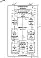
- FIG. 1is a drawing of an example communications device 100 including self-interference cancellation capability in accordance with an example embodiment.
- Example communications device 100includes a transceiver circuit 102 , a processor 109 , e.g., a CPU, a memory 106 , and an assembly of modules 118 , e.g., assembly of hardware modules, e.g., circuits, coupled together via a bus 108 , over which the various elements 102 , 109 , 106 , 118 , may communicate data and information.
- a transceiver circuit 102includes a transceiver circuit 102 , a processor 109 , e.g., a CPU, a memory 106 , and an assembly of modules 118 , e.g., assembly of hardware modules, e.g., circuits, coupled together via a bus 108 , over which the various elements 102 , 109 , 106 , 118 , may communicate data and information.
- modules 118
- Memory 106includes a communications routine 110 configured to control communications operations for the communications device 100 including controlling operation of the transceiver circuit 102 , a control routine 111 , an assembly of modules 113 , e.g., an assembly of software modules, and data/information 114 .
- Data/information 114includes device information 119 , which includes. e.g., interface information including optical filter component information and antenna information, etc., and communications data/information 120 which includes, e.g., RF frequency information, channel type information, channel conditions, determined filter coefficients, received signal information, transmitted signal information, generated radio frequency interference cancellation signal information, etc.
- some information stored in memory 106is also stored in local memory within transceiver circuit 102 .
- processor 109executes routines including software modules included in memory 106 to control the communications device 100 to implement a method in accordance with the present invention, e.g., control the transceiver circuit 102 to implement a radio frequency interference cancellation method which includes the use of an optical filter assembly.
- routines including software modules included in memory 106to control the communications device 100 to implement a method in accordance with the present invention, e.g., control the transceiver circuit 102 to implement a radio frequency interference cancellation method which includes the use of an optical filter assembly.
- one or more of steps of the example methodare implemented alternatively by one or more hardware modules, e.g., circuits, included in assembly of modules 118 .
- Transceiver circuit 102includes a bus interface 107 and a communications interface 113 .
- Bus interface 107couples the transceiver circuit to bus 108 .
- Communications interface 113couples the transceiver circuit 102 to one or more or all of: an antenna assembly 101 , a waveguide 115 and a wire/cable 117 .
- the antenna assembly 101is included as part of the communications device 100 .
- Antenna assembly 101includes one or more antennas ( 103 , . . . , 106 ).
- antenna assembly 101includes a single antenna 103 which is used by both the transmitter and receiver of the transceiver circuit 102 .
- the antenna assembly 101includes a transmit antenna 103 and a receive antenna 106 . In some embodiments, the antenna assembly 101 includes a plurality of transmit antennas and a plurality of receive antennas. In some such embodiments, the antenna assembly 101 and the transceiver circuit 102 support MIMO operations.
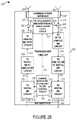
- FIG. 2Aillustrates an example transceiver circuit 102 ′ in accordance with an example embodiment.
- Transceiver circuit 102 ′includes communications interface 113 ′ and bus interface 107 .
- transceiver circuit 102 ′is transceiver circuit 102 of FIG. 1
- communications interface 113 ′is communications interface 113 of FIG. 1 .
- FIG. 2B and FIG. 2Cillustrate two example variants of a wireless transceiver architecture that includes one transmit chain and one receiver chain.
- the realization shown in drawing 200 of FIG. 2Billustrates a two antenna approach where the transmitter chain and the receiver chain use separate antennas 229 , 231 , respectively.
- the coupling between transmit and receiveis driven by the distance between the antennas, the antenna type and size.
- the transmit chain and the receive chainuse a single antenna 230 .
- the antenna 230is coupled to the transmit and receive chains using a circulator 225 where the circulator provides some degree of isolation between the transmit signal 227 and receive signal 233 .
- the high power self-interference seen at the receive chainis driven by the isolation provided by the circulator 225 and the reflection from the antenna 230 that leaks back in to the receive chain.
- Transceiver circuit 102 ′′is, e.g., transceiver circuit 102 of FIG. 1 and/or transceiver circuit 102 ′ of FIG. 2 .
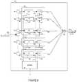
- Transceiver circuit 102 ′′includes communications interface 113 ′′, bus interface 107 , transmit (TX) digital baseband (BB) circuit 206 , TX digital BB to analog BB circuit 204 , TX analog BB to radio frequency (RF) circuit 202 , coupler device 226 , signal combiner/coupler device 209 , RX RF to analog BB circuit 210 , RX analog BB to digital BB circuit 212 , RX digital BB circuit 214 , RF up-converter and interference cancellation filter circuit 222 , and channel estimator, filter, e.g., digital filter, and filter control circuit 216 , coupled together as shown in FIG. 2B .
- TXtransmit
- BBdigital baseband
- RFradio frequency
- Signal combiner 209is configured to combine a received radio frequency signal 233 with the radio frequency interference cancellation signal 224 to produce a recovered radio frequency signal 235 .
- the signal combiner 209is configured to add the radio frequency interference cancellation signal 234 to the received radio frequency signal 233 to generate the recovered radio frequency signal 235 .
- the transceiver circuit 102 ′′comprises of a transmit chain and the receive chain.
- the transmit digital baseband circuit 206receives, via bus interface 107 , input data 207 to be transmitted in the form of bits, converts the bits into a digital baseband waveform 205 , which is output to the TX digital BB to analog BB circuit 204 .
- the TX digital baseband circuit 206performs encoding and modulation of the received input data 207 .
- the encoding and modulation performed by TX digital baseband circuit 206uses, e.g. orthogonal frequency division multiplexing, CDMA, or another encoding and modulation scheme.
- the TX digital BB to analog BB circuit 204e.g., a filter and digital to analog converter (DAC) assembly, converts the digital signal 205 into analog baseband signal 203 , which is output to TX analog BB to RF circuit 202 .
- DACdigital to analog converter
- Analog baseband signal 203is received by TX analog BB to RF circuit 202 and subsequently upconverted to the operating RF frequency using a direct conversion or an intermediate frequency converter included in circuit 202 .
- the up-converted RF signal 201is the output of a power amplifier included in circuit 202 .
- the up-converted RF signal 201is coupled or divided using a device 226 where the pass-through signal 227 goes to the communication interface 113 ′′ and the tapped signal 223 is fed to the RF up-converter and interference cancellation filter circuit 222 .
- the RF signal 227 in the communication interface 113 ′′passes through to the antenna 229 in case of this realization.
- Receive antenna 231receives a wireless RF signal and outputs received signal 233 into in to interface 113 ′′ toward the receive chain.
- the receive signal 233 from the communication interface 113 ′′feeds in to a coupler or combiner 209 which is 3 port device.
- Coupler or combiner 209is responsible for combining input signal 224 , which is an output of the RF-up converter and interference cancellation filter circuit 222 , and input signal 233 , which is the signal received via receive antenna 231 , to generate output RF signal 235 .
- the output RF signal 235is fed into the RX RF to analog BB circuit, 210 , which is an RF down-converter, that down-converts the RF signal 235 into a baseband analog signal 211 .
- This baseband analog signal 211is received, filtered and sampled by RX analog BB to digital BB circuit 212 , which generates and outputs sampled output signal 213 .
- the sampled output signal 213is fed into the RX digital BB circuit 214 including a digital receive processor that is responsible for demodulation and decoding.
- a copy of the transmit signal 201is fed into the RF up-converter and interference cancellation filter circuit 222 .
- the RF Up-converter and interference cancellation filter circuit 222produces signal 224 which is a negative copy or near negative copy of the interference signal received as a component of receive signal 233 , said interference signal being an effect of transmission of signal 227 .
- the combining of the negative copy 224 with the received signal 233 using a combiner/coupler device 209results in cancellation of interference that is caused by the transmitter of transceiver circuit 102 ′′ at the receiver of transceiver circuit 102 ′′.
- Channel estimator, filter and filter control circuit 216interfaces with the digital processing block of transmit digital baseband circuit 206 and with the digital processing block of receive digital baseband circuit 214 .
- the channel estimator, filter, and filter control circuit 216is responsible for reconstruction of the residual interference signal that is observed at the sampled signal 220 in the RX digital baseband circuit 214 .
- the channel estimator, filter and filter control circuit 216is responsible for the measurement and training of a digital filter included in circuit 216 and the RF cancellation filter included in circuit 222 .
- Channel estimator, filter, and filter control circuit 216uses input signal 219 , a copy of the digital transmit signal, and received sampled signal 220 to determine the effect of the transceiver circuit 102 ′′ and antennas ( 229 , 231 ), determine the channel that causes interference, and determine the appropriate coefficients to be programmed to the RF interference cancellation filter included in circuit 222 .
- the determined appropriate coefficientsare communicated in signal 217 from channel estimator, filter and filter control circuit 216 to RF up-converter and interference cancellation filter circuit 222 .
- Channel estimator, filter and filter control circuit 216also recreates a negative copy 221 of the interference signal, which it sends to RX digital BB circuit 214 to be subtracted from the received signal 213 .
- RX digital BB circuit 214receives the recreated negative copy 221 of the interference signal and subtracts the recreated negative copy 221 of the interference signal from received signal 213 , as part of its processing. Circuit 214 further generates digital data out signal 215 and outputs digital data out signal via interface 107 .
- Drawing 200 ′ of FIG. 2Cillustrates example transceiver circuit 102 ′′′ which implements a transceiver architecture where the communications interface 113 ′′′ includes a 3-port circulator device 225 .
- the circulator 225is responsible for the creation of isolation between the ports in one direction. This created isolation prevents the transmit RF signal 227 leaking to the receive RF signal 233 .
- the circulator based designfacilitates simultaneous transmission and reception using a single antenna 230 .
- Transceiver circuit 102 ′′′is, e.g., transceiver circuit 102 of FIG. 1 and/or transceiver circuit 102 ′ of FIG. 2 .
- Transceiver circuit 102 ′′′includes communications interface 113 ′′′ which includes circulator 225 , bus interface 107 , transmit (TX) digital baseband (BB) circuit 206 , TX digital BB to analog BB circuit 204 , TX analog BB to radio frequency (RF) circuit 202 , coupler device 226 , combiner/coupler device 209 , RX RF to analog BB circuit 210 , RX analog BB to digital BB circuit 212 , RX digital BB circuit 214 , RF up-converter and interference cancellation filter circuit 222 , and channel estimator, filter, e.g., digital filter, and filter control circuit 216 , coupled together as shown in FIG. 2C .
- TXtransmit
- BBdigital baseband
- RFradio frequency
- Signal combiner 209is for combining a received radio frequency signal 233 with the radio frequency interference cancellation signal 224 to produce a recovered radio frequency signal 235 .
- the signal combiner 209is configured to add the radio frequency interference cancellation signal 224 to the received radio frequency signal 233 to generate the recovered radio frequency signal 235 .
- the transceiver circuit 102 ′′′comprises a transmit chain and the receive chain.
- the transmit digital baseband circuit 206receives, via bus interface 107 , input data 207 to be transmitted in the form of bits, converts the bits into a digital baseband waveform 205 , which is output to the TX digital BB to analog BB circuit 204 .
- the TX digital baseband circuit 206performs encoding and modulation of the received input data 207 .
- the encoding and modulation performed by TX digital baseband circuit 206uses, e.g. orthogonal frequency division multiplexing, CDMA, or another encoding and modulation scheme.
- the TX digital BB to analog BB circuit 204e.g., a filter and digital to analog converter (DAC), converts the digital signal 205 into analog baseband signal 203 , which is output to the transmit analog baseband to RF (TX analog BB to RF) circuit 202 .
- Analog baseband signal 203is received by the TX analog BB to RF circuit 202 and subsequently up-converted to the operating RF frequency using a direct conversion or an intermediate frequency converter included in circuit 202 .
- the signal 201is the output of a power amplifier included in circuit 202 .
- the up-converted RF signal 201is coupled or divided using a device 226 where the pass-through signal 227 goes to the communication interface 113 ′′′ and the tapped signal 223 is fed to the RF up-converter and interference cancellation filter circuit 222 .
- the RF signal 227 in the communication interface 113 ′′′passes through circulator 225 to the antenna 230 in case of this realization.
- Antenna 230receives a wireless RF signal and outputs received signal into circulator 225 of interface 113 ′′′, which sends the received signal 233 toward the receive chain.
- the receive signal 233 from the communication interface 113 ′′′feeds into a coupler or combiner 209 which is 3 port device.
- Coupler or combiner 209is responsible for combining input signal 224 , which is an output of the RF-up converter and interference cancellation filter circuit 222 , and input signal 233 , which is the signal received via antenna 230 , to generate output RF signal 235 .
- the output RF signal 235is fed into the RX RF to analog BB circuit 210 , which is an RF down-converter, that down-converts the RF signal 235 into a baseband analog signal 211 .
- This baseband analog signal 211is received, filtered and sampled by RX analog BB to digital BB circuit 212 , which generates and outputs sampled output signal 213 .
- the sampled output signal 213is fed into the RX digital BB circuit 214 including a digital receive processor that is responsible for demodulation and decoding.
- RF Up-converter and interference cancellation filter circuit 222produces signal 224 which is a negative copy or near negative copy of the interference signal received as a component of receive signal 233 , said interference signal being an effect of transmission of signal 227 .
- the combining of the negative copy 224 with the received signal 233 using a combiner/coupler device 209results in cancellation of interference that is caused by the transmitter of transceiver circuit 102 ′′′ at the receiver of transceiver circuit 102 ′′′.
- Channel estimator, filter and filter control circuit 216interfaces with the digital processing block of transmit digital baseband circuit 206 and with the digital processing block of receive digital baseband circuit 214 .
- the channel estimator, filter, and filter control circuit 216is responsible for reconstruction of the residual interference signal that is observed at the sampled signal 220 in the RX digital baseband circuit 214 .
- the channel estimator, filter and filter control circuit 216is responsible for the measurement and training of a digital filter included circuit 216 and the RF cancellation filter included in circuit 222 .
- Channel estimator, filter, and filter control circuit 216uses input signal 219 , a copy of the digital transmit signal, and received sampled signal 220 to determine the effect of the transceiver circuit 102 ′′′ and antenna 230 , determine the channel that causes interference, and determine the appropriate coefficients to be programmed to the RF interference cancellation filter included in circuit 222 .
- the determined appropriate coefficientsare communicated in signal 217 from channel estimator, filter and filter control circuit 216 to RF up-converter and interference cancellation filter circuit 222 .
- Channel estimator, filter and filter control circuit 216also recreates a negative copy 221 of the interference signal, which it sends to RX digital BB circuit 214 to be subtracted from the received signal 213 .
- RX digital BB circuit 214receives the recreated negative copy 221 of the interference signal and subtracts the recreated negative copy 221 of the interference signal from received signal 214 , as part of its processing. Circuit 214 further generates digital data out signal 215 and outputs digital data out signal via interface 107 .
- Drawing 200 ′ of FIG. 2Cillustrates example transceiver circuit 102 ′′′ which implements a transceiver architecture where the communications interface 113 ′′′ includes a 3-port circulator device 225 .
- the circulator 225is responsible for the creation of isolation between the ports in one direction. This created isolation prevents the transmit RF signal 227 leaking to the receive RF signal 233 .
- the circulator based designfacilitates simultaneous transmission and reception using a single antenna 230 .
- FIG. 2D and FIG. 2E diagrams 200 ′′ and 200 ′′′show example dual/multi chain radios.
- the diagram 200 ′′′ in FIG. 2Dshows two transmit chains and two receive chains connected to the communication interface 113 ′′ and 113 ′′′′.
- the transmit antenna 229is radiating a signal 227 at the frequency A while the receive antenna 231 is receiving the signal 233 at frequency B.
- the transmit antenna 229 ′is radiating the signal 227 ′ at the frequency B while the receive antenna 231 ′ is receiving signal 233 ′ at the frequency A.
- the signal 227 from antenna 229causes interference at the antenna 231 ′, while the signal 227 ′ radiated from antenna 229 ′ interferes at the receiver 231 .
- the configuration shown herecan be understood as a case of two frequency division duplex operation capable radios operating together where one radio transmits at frequency A and receives at frequency B while the other radio transmits at frequency B while receiving at frequency A.
- the copy signal 223 of the transmit signal 227 going to antenna 229feeds to the RF upconverter and interference cancelation circuit 222 which processes and shapes the signal to reflect the interference signal characteristic seen at the receive antenna 231 ′ as signal 233 ′.
- the reconstructed signal 224 ′e.g., an interference cancellation signal, which is an approximate negative copy of the interference signal is added to the received signal 233 ′ at 209 ′.
- the channel estimator, filter and filter control circuit 216interfaces with the TX digital baseband circuit 206 , sending digital transmit signal 218 to the TX digital baseband circuit 206 and receiving signal 219 from the TX Digital BB Circuit 206 .
- the channel estimator, filter and filter control circuit 216also interfaces with the TX digital baseband circuit 214 ′, receiving the digital signal 220 ′ from RX digital BB circuit 214 ′ and sending signal 221 ′ to the RX digital BB circuit 214 ′.
- the filter control circuit 216provides the coefficients 217 to the RF up-converter and interference cancelation filter circuit 222 .
- the copy signal 223 ′ of the transmit signal 227 ′ going to transmit antenna 229 ′feeds to the RF upconverter and interference cancelation filter circuit 222 ′ that processes signal 223 ′ to create the reconstructed signal 224 .
- the output signal 224 from the RF upconverter and interference cancelation filter 222 ′is added to the receive signal 233 that contains the interference.
- FIG. 2E diagram 200 ′′′shows an arrangement of various blocks in 102 ′′′′ similar to that of 102 ′′′ in FIG. 2D with one distinction that the communication interface connects the transmit and receive chain to a single antenna on each side.
- the blocks 222 and 216are elements, e.g., two stages, of interference reconstruction where the main function of these two structures is to delay/buffer a copy of the transmit signal 223 and filter it such that its output 224 represents an accurate reconstruction of the self-interference signal 233 that can be combined using 209 with a received signal 233 in the receiver chain.
- Each filter 216 , 222may generate different portions of the received signal to be used cancel different portions of the interference.
- the different portionsmay correspond to self-interference corresponding to different amounts of signal delay.
- the ability to accurately delay the signal corresponding to many or all received copies due to reflections from objects in the environmentcan be useful when performing interference cancelation.
- various approaches in RF, surface acoustic wave, photonic, phonon—photonic, slow light and RF MEMS based switchesare used in novel configurations and unique manner to present a unique architecture where a combination of one or more of these techniques can be used to achieve the degree of self-interference cancellation desirable for a full duplex operation.
- the use of surface acoustic wave and photonic techniques to generate delayed versions of a signalmay be useful for supporting delays of durations which might be otherwise difficult to support.
- RF photonicsmay, and sometimes does, involve a hybrid approach that involves processing RF signals at optical domains.
- analog RF signaldefines the envelope of an optical carrier wave, typically around 200 THz. Therefore, even multi-GHz ultra-wideband signals occupy a fractional bandwidth of less than 10-5.
- millimeter-wave baseband frequenciesare far smaller than the typical bandwidth of optical components. Therefore, RF photonics is a powerful approach that is transparent to the RF baseband frequency, provided that a broadband modulator is used.
- optical delay lines in the form of optical fiberscan be coiled into centimeter loops, and multiple delay lines can be stacked together vertically, and packed into a footprint that is 4 to 5 times smaller than microwave delay lines for a 12-tap cancellation filter.
- increasing the tap number from 12 to 64 in a RF-photonic filteronly increases the height of the system, and allows for much better analog cancellation without increasing system footprint.
- Another important feature of a RF photonic linkis its fundamentally unidirectional nature, i.e. the signal path is fixed from the optical modulator (RF-to-optics) towards the optical detector (optics-to-RF), since neither device operates in a reversible fashion.
- RF photonic systemsalso enjoy several additional advantages unique to its hybrid architecture.
- a laser sourceprovides an overall gain to the RF transfer function, which can be adjusted on demand.
- full complex-valued filter coefficientscan be realized by adjusting the optical phase, which only requires sub-micron displacement and can be realized with time constants less than 1 micro second.
- on-chip optical signal processinghas been realized via opto-mechanical, also sometimes referred to as optomechanical, effects: an mm scale chip can provide the same processing power which previously required 100 meters of optical fibers.
- Metrics and features of the present invention and the proposed approachdoes well include: Delay bandwidth: the optical bandwidth over which a certain delay can be achieved; Maximum delay: the maximum achievable delay value; Fractional delay: the absolute delay value divided by the pulse width or bit time. This is important to the delay/storage capacity; Delay range: the tuning range that the delay can be achieved (from minimum value to maximum achievable value); Delay resolution: the minimum incremental delay tuning step; Delay accuracy: the precision percentage of the actual delay to that of the desired delay value; Delay reconfiguration time: the amount of time it takes to switch a delay from one state to another steady state; Loss over delay: The amount of loss incurred per unit delay. Lower loss per unit delay is desired.
- Silicon nitrateis used for a modulator that can transform the RF signal using a piezo structure to convert the RF signal to the optical domain.
- This modulatorwill be able to delay the signal based on the change of heaters/reception area/wavelength of the acoustic receptors for absorption of phonons into the optical waveguide.
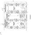
- FIG. 4describes a high level architecture of the block 122 , i.e., the up-conversion and cancellation filter, for self-interference cancellation.
- the blocks 181 , 182 and 183are example filter banks implemented in accordance with the invention.
- the bank 183reconstructs the direct path
- bank 182reconstructs the antenna path
- bank 181reconstructs the scatter path.
- An example apparatus for up conversion or down conversion of RF signal for signal processingmay, in some but not necessarily all embodiments, have one or more of the following features and/or is configured to in the following example manner: uses a modulator to up convert the signal the above modulator can be fed with a light source such as laser/LED; uses a directly modulated laser; the RF signal can be applied to a piezo-structure that converts the RF signal to acoustic signal this piezo structure then transfers the RF signal over to an optical carrier fed in by a light source.
- a modulatoruses a modulator to up convert the signal the above modulator can be fed with a light source such as laser/LED; uses a directly modulated laser; the RF signal can be applied to a piezo-structure that converts the RF signal to acoustic signal this piezo structure then transfers the RF signal over to an optical carrier fed in by a light source.
- the apparatusmay include elements that delay photonics signals.
- the elementsmay, and in some embodiments do, include photon-phonon hybrid device that delays the signal using the speed of acoustic waves. These elements may or may not be tunable for the amount of delay they provide the apparatus may have n-dimensional array of these delay elements the array can be configured to provide the required delay by switching on/off the delay elements or, if capable, configuring each delay elements to achieve a total delay for the desired value.
- the apparatusin some embodiments is configured to do one or more of the following: operate on a wavelength division multiplexing laser and each wavelength is uniquely fed to an array of delay elements; the delayed optical signal is combined before the detector using an optical combiner, or each of the delayed signal in an array is fed through optical detector where RF signals from each branch is combined using transmission lines; Division of the cancellation delay element in two, three or more stages; Support Micro seconds of delay using a mm size architecture; Support a Slow light architecture; can use RF MEMS based switches; Switch-based banks; Feedback to RF-photonics and MEMS switches (Flowchart diagram); a Calibration algorithm is supported in some embodiments; digital cancellation and interface with digital cancellation can be supported
- the level of interference cancellation requiredvaries for different wireless deployment applications.
- about 98 dB of interference cancellationis required for simultaneous transmit and receive operation.
- the limit of digital cancellation in such a caseis about 42 dB due to the limitation of dynamic range of the type of analog-to-digital converters used in these systems.
- Three other scenarios for mobile transmission, small cell transmission and base station transmissionwhere the typical transmit power is 23 dBm, 24 dBm and 46 dBm respectively.
- the digital cancellationis limited by the dynamic range of the analog to digital converters used.
- the remaining interferenceneeds to be cancelled in the analog/RF domain.
- FIG. 2Ddescribes the operation of a multiple antenna radio capable of simultaneous transmission and reception. It depicts the applicability of the self-interference cancellation architecture with filters 222 and 216 that allows for interference cancellation between multiple transmit antenna to multiple receive antenna. Such a radio requires multiple instantiation of filters 222 and 216 to reconstruct and cancel interference caused by multiple transmit and receive antenna. These multiple instantiations can be, and in some embodiments are, optimized and packaged together as one instantiation with inputs from multiple transmit radios to multiple receive radios. This depiction shows 2 transmit and 2 receive antenna. However, the principle applies to plurality of transmit and receive antenna.
- FIG. 3Ais a diagram of a wireless device in an environment and is intended to facilitate an understanding of the problem of self-interference in wireless radio systems capable of simultaneous transmission and reception using a transceiver such as the one shown in FIG. 2B where transmission and reception are via separate receive and transmit antennas 229 , 231 , respectively.
- a transceiversuch as the one shown in FIG. 2B where transmission and reception are via separate receive and transmit antennas 229 , 231 , respectively.
- Direct Pathdepicted by 301 in FIG. 3A , where the transmission signal couples with the receiver at either on the circuit board due to radiation across transmission lines or through the circulator as shown in case of a single antenna architecture.
- This direct path signalis roughly about 15-25 dB lower than the transmit power radiating out of the transmit antenna.
- This pathis also the shortest path of interference from transmit to the receive chain with the delay between 229 and 231 expected to be in the order of 10s of Pico seconds to 100s of Pico seconds depending on the architecture of a radio.
- This direct pathis a time varying frequency selective channel where these characteristics depend on the PVT characteristic of operation. (Pressure, Volume (doping and size of the transmission lines), Temperature.)
- the second path of interferenceis Antenna Path, the shortest path between the transmitter and receiver antenna by which a transmitted signal reach the antenna being used for receiving signals.
- this interference pathwill normally be the path 301 which corresponds to the distance between the transmit antenna 229 and receive antenna 231 .
- the antenna pathis the path 302 ′ taken by the transmit signal in the near-field of the antenna after reflection. The reflections from the antenna can be due to the mismatch in the impedance.
- the Antenna Pathis time varying and frequency selective. The signal received from this path is roughly 20-45 dB lower than the transmit power of the signal with the path delay in the range of 400 picoseconds to 1.5 nanoseconds based on the radio and antenna design.
- the third main principle path of self-interferenceis the Scatter Path.
- the transmitted signals 303 in this pathtravel from the transmit antenna 229 to the environment 305 and echo back as reflections 304 from environmental objects 305 which operate as signal scatters.
- This pathis also time varying and most frequency selective among the three paths.
- the overall path delayis very wide depending on the environment around the radio, roughly between 10s of nanosecond to 5 microseconds.
- the signals from this pathare received with 50 dB or lower below the transmit power depending on the frequency of operation and path loss in the environment.
- the RF self-interference cancellation architecture described hereinis designed to reconstruct the self-interference by tracking and applying characteristic of the direct path, antenna path and scatter path to a copy of signal 223 resulting in interference cancellation signal 224 and adding interference cancellation signal 224 to the received signal at 209 .
- FIG. 4 diagramshows categorization of reconstruction of the self-interference for these three paths as 181 , 182 , and 183 based on the amount of delay required to reconstruct the interference signal.
- the blocks 181 , 182 and 183have delay elements that are tunable from a controller through a voltage/current controlled interface bus 191 .
- Block 181includes delay elements ( 402 , 403 , . . . , 405 ) which are tunable via control signals ( 421 , 422 , . . . , 423 ), respectively, from controller 401 communicated through bus 191 .
- Block 182includes delay element 406 which is tunable via control signal 424 from controller 401 communicated through bus 191 .
- Block 183includes delay element 407 which is tunable via control signal 425 from controller 401 communicated through bus 191 .
- the inputs of delay elements ( 402 , 403 , . . . , 405 , 406 , 407 )are signals ( 426 , 427 , . . . , 428 , 429 , 430 ), respectively, and the outputs of delay elements ( 402 , 403 , . . . , 405 , 406 , 407 ) are signals ( 436 , 437 , . . . , 438 , 439 , 440 ), respectively
- FIG. 4also shows attenuation/amplification devices ( 408 , 409 , . .
- the attenuation/amplification devices( 408 , 409 , . . . , 410 , 411 , 412 ) are also controlled by controller 401 through voltage/current interface bus 192 via control signals ( 431 , 431 , . . . , 433 , 434 , 435 ), respectively.
- coefficients communicated in signals( 431 , 432 , .
- the elements 184 , 185 , 186 , 187 , 188 , 189are elements that route the same RF signals 223 from input to multiple outputs ( 426 , 427 , 428 , 429 , 430 ). These elements ( 184 , 185 , 186 , 187 , 188 , 189 ) can be, and in some embodiments are, RF power dividers or balun circuits (balanced-unbalanced) or another RF element with the routing capability.
- Element 190is an element that combines multiple RF signals ( 450 , 451 , 452 , 453 , 454 ) together to generate signal 224 .
- Element 190can be, and in some embodiments is, a multi-port RF power combiner or an array of RF combiners to sum the signals together.
- FIG. 5includes drawings 501 , 502 and 503 , illustrating three scenarios of simultaneous transmission and reception operation where self-interference cancellation can improve the operation of a radio device: in-band operation depicted in drawing 501 by 510 and 511 , overlapping band operation as shown in drawings 502 by 512 and 513 , and adjacent band operation depicted in drawing 503 by 514 and 515 .
- in-band operation depicted in drawing 501 by 510 and 511overlapping band operation as shown in drawings 502 by 512 and 513
- adjacent band operation depicted in drawing 503 by 514 and 515depicts the ability to cancel the interference arising from a transmission allows the radio to operate in the appropriate dynamic range to demodulate and decode the intended receive signal.
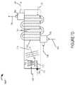
- FIG. 6Adepicts an example novel architecture of a optical modulator, signal delay and signal gain block 652 which can be used as the signal reconstruction bank 181 , 182 or 183 of FIG. 4 or can be used in various other embodiments shown in the present application.
- the reconstruction banksare responsible for operations on the input including delay used to cause a signal delay and a multiply used to control signal gain and thus how much an impact the delayed signal generated by block 652 will contribute to the overall composite output generated by combining the output of signal delay and gain control blocks 652 .
- Optical modulator, signal delay and signal gain block 652includes an optical-mechanical modules 611 , delay element X 613 , delay element Y 11 615 , delay element YIN 616 , optical waveguide 618 , and gain element A 1 619 .
- Delay control signal DC_X 1 683controls delay element X 613 .
- Delay control signal DC_Y 11 685controls delay element Y 11 615 .
- Delay control signal YIN 686controls delay element YIN 616 .
- Input laser light signal 688is received by optical waveguide 618 .
- Gain Control (GC) signal 689controls gain element A 1 619 .
- FIG. 6Bshows an example RF up-converter and interference cancelation filter circuit 222 that can be used in the system of FIG. 2B or 2C and which can be implemented using multiple modulation, delay and gain control blocks, e.g., N of such blocks, of the type shown in FIG. 6A along with various other components such as controller 654 and laser 655 .
- Controller 654receives signal 217 from channel estimator, filter and filter control circuit 216 and uses the information communicated in signal 217 including, e.g., determined coefficient values.
- RF up-converter and interference cancelation filter circuit 222includes multiple lasers, e.g., laser 655 which generates laser light signal 688 and laser n 655 ′ which generates laser light signal 688 ′.
- one of the laser light signals 688 or 688 ′is used an the input to an optical waveguide, e.g., optical waveguide 618 , at a particular time.
- Component block 652includes an optical mechanical module 611 with an output 612 that is coupled to a series arrangement of delays x 1 613 , Y 11 615 through Y 1 N 616 where N is used to represent an integer number greater than 1.
- the delaysare controllable in the FIG. 6A embodiment but it should be appreciated that one or more of the delays could be of a fixed amount.
- the first delay element 613is controlled by delay control (DC) signal DC_X 1 683 .
- the second delay element 615is controlled by delay control (DC) signal DC_Y 11 685 .
- the Nth delay element 616is controlled by delay control (DC) signal DC_Y 1 N 686 .
- the output of the series of delay elementsis provided to an optical waveguide 618 for transduction from mechanical waves to optical carrier which receives as an input a laser light signal LL 688 prior to being subject to a gain control operation performed by multiplier A 1 619 .
- the gain operation performed by element 619is controlled by gain control signal GC 689 .
- the delay element control signals683 , 683 ′, 683 ′′, . . . , 683 ′′′, 685 , 685 ′, 685 ′′, . . . , 685 ′′′, . . .
- Gain control signals(GC 1 689 , GC 2 689 ′, GC 3 689 ′′, . . . , GCN 689 ′′′), communicated from controller 654 via gain control bus 672 , are used to control gain control elements (A 1 619 , A 2 619 ′, A 3 619 ′′, . . . , AN 619 ′′′), respectively.
- FIG. 6Bthere are N implementations of block 652 with the elements of the first block 652 being surrounded by a box for illustration purposes.
- the boxis omitted from block 652 ′ corresponding to the second row of elements, block 652 ′′ corresponding to the third row of comments and block 652 ′′′ corresponding to the Nth row of components for space and illustration purposes.
- FIG. 6Bdescribes device design of the RF up-converter and interference cancelation filter circuit 222 of FIG. 2B to 2E .
- the main idea of the design architecture presented in FIG. 6Bis to realize a novel RF signal processing circuit that can be built using elements 611 , 613 , 615 , 616 , 618 , 619 , 620 , 660 .
- the device 222has an input RF signal 223 that connects to the element 186 in the device 222 .
- the element 186can be a power divider/splitter/balanced-unbalanced circuit that can split the signal in to two or more arms that contain a copy of the input signal with possibly varying degree of amplitudes.
- the output of the element 186can go to other elements such as element 185 - and element 187 , which are similar in function to element 186 .
- An first output of element 185goes to element 184 and a second output of element 185 , signal 610 ′, is an input to opto-mechanical modulator 611 ′.
- An output of element 185is output signal 610 , which is an input signal for opto-mechanical modulator 611 .
- An first output of element 187goes to element 188 and a second output of element 187 , is signal 610 ′′, which is an input to opto-mechanical modulator 611 ′′.
- An output of element 188is output signal 610 ′′′, which is an input signal for opto-mechanical modulator 611 ,
- the output signal 610 of element 184goes to device 652 that converts, via opt-mechanical modulator 611 , the input signal 610 to mechanical wave 612 and then ultimately to the optical signal through the element 618 , an optical waveguide that allows transduction of mechanical waves to optical carrier that in turn transfers the RF signal 610 over to the optical carrier from the laser 655 .
- the mechanical signal 612 that includes the RF input signal 610can be, and in some embodiments is, delayed using the delay elements ( 613 , 615 , . . . 616 ).
- the delaycan be, and in some embodiments is, configured using the delay control (DC) signals ( 683 , 685 , . . . 686 ) from the controller 654 .
- the amplitude of the optical signal out from the optical waveguide 618can be tuned by the element 619 .
- the output optical signal from the element 619then undergoes optical to electrical conversion in the element 620 .
- the output signal 610 ′ of element 185goes to device 652 ′ that converts, via opt-mechanical modulator 611 ′, the input signal 610 ′ to mechanical wave 612 ′ and then ultimately to the optical signal through the element 618 ′, an optical waveguide that allows transduction of mechanical waves to optical carrier that in turn transfers the RF signal 610 ′ over to the optical carrier from the laser 655 .
- the mechanical signal 612 ′ that includes the RF input signal 610 ′can be, and in some embodiments is, delayed using the delay elements ( 613 ′, 615 ′, . . . 616 ′).
- the delaycan be, and in some embodiments is, configured using the delay control (DC) signals ( 683 ′, 685 ′, . .
- the amplitude of the optical signal out from the optical waveguide 618 ′can be tuned by the element 619 ′.
- the output optical signal from the element 619 ′then undergoes optical to electrical conversion in the element 620 ′.
- the output signal 610 ′′ of element 187goes to device 652 ′′ that converts, via opt-mechanical modulator 611 ′′, the input signal 610 ′′ to mechanical wave 612 ′′ and then ultimately to the optical signal through the element 618 ′′, an optical waveguide that allows transduction of mechanical waves to optical carrier that in turn transfers the RF signal 610 ′′ over to the optical carrier from the laser 655 .
- the mechanical signal 612 ′′ that includes the RF input signal 610 ′′can be, and in some embodiments is, delayed using the delay elements ( 613 ′′, 615 ′′, . . . 616 ′′).
- the delaycan be, and in some embodiments is, configured using the delay control (DC) signals ( 683 ′′, 685 ′′, . .
- the amplitude of the optical signal out from the optical waveguide 618 ′′can be tuned by the element 619 ′′.
- the output optical signal from the element 619 ′′then undergoes optical to electrical conversion in the element 620 ′′.
- the output signal 610 ′′′ of element 188goes to device 652 ′′′ that converts, via opt-mechanical modulator 611 ′′′, the input signal 610 ′′′ to mechanical wave 612 ′′′ and then ultimately to the optical signal through the element 618 ′′′, an optical waveguide that allows transduction of mechanical waves to optical carrier that in turn transfers the RF signal 610 ′′′ over to the optical carrier from the laser 655 .
- the mechanical signal 612 ′′′ that includes the RF input signal 610 ′′′can be, and in some embodiments is, delayed using the delay elements ( 613 ′′′, 615 ′′′, . . . 616 ′′′).
- the delaycan be, and in some embodiments is, configured using the delay control (DC) signals ( 683 ′′′, 685 ′′′, . . . 686 ′′′) from the controller 654 .
- the amplitude of the optical signal out from the optical waveguide 618 ′′′can be tuned by the element 619 ′′′.
- the output optical signal from the element 619 ′′′then undergoes optical to electrical conversion in the element 620 ′′′.
- Device 222 of FIG. 6Bincludes stacked detectors and MEMS switch component 656 .
- Component 656includes the optical to electrical conversion devices (O/E 620 , O/E 620 ′, O/E 620 ′′, . . . , O/E 620 ′′′), coupled to controllable MEMS switches (MEMS switch 1660 , MEMS switch 2 661 , MEMS switch 3 662 , . . . , MEMS switch N 663 ), respectively.
- MEMS switchesMEMS switch 1660 , MEMS switch 2 661 , MEMS switch 3 662 , . . .
- switch control signalsSC 1 691 , SC 2 691 ′, SC 3 691 ′′, . . . , SCN 691 ′′′
- controller 654via switch control bus 671 .
- Componentfurther includes combiner element 190 which receives RF output outputs signals from the outputs of one or more O/Es ( 620 , 620 ′, 620 ′′, . . . , 620 ′′′), which pass through the switches, which are being controlled to be closed at a given time, and generates RF output signal 224 .
- combiner element 190which receives RF output outputs signals from the outputs of one or more O/Es ( 620 , 620 ′, 620 ′′, . . . , 620 ′′′), which pass through the switches, which are being controlled to be closed at a given time, and generates RF output signal 224 .
- FIGS. 6A, 6B, 7A, 7B, 7C and 7Dtake advantage of the fact that signal delay and/or the control of how much signal delay is achieved, can take advantage of the fact that that sound waves travel 105 times slower than RF electromagnetic waves.
- the principle working of one of the arms, e.g., optical modulator, delay and gain blocks 652will now be described in with reference to FIGS. 7A-D which show various example devices that perform optical to mechanical modulation, signal delay, and/or gain control which in some embodiments may be, and often is, controlled.
- the different embodiments shown in FIG. 7A to 7Dmay use different approaches to one or more of the functions implemented by a signal processing block, e.g., block 652 .
- FIG. 7Aillustrates a device 700 which can be used as block 652 of FIG. 6A .
- the high level function of the device 700is to convert the input RF signal 610 from the analog RF signal to the acoustical signal 701 using a piezo-structure or an opto-mechanical structure 702 which then uses the phenomenon of phonon-photon transduction to transfer the RF signal 610 from acoustical signal 701 over to the optical carrier 705 or 706 that is travelling over the waveguide 709 .
- the orientation at which the signal 701will affect where the signal reaches the waveguide 709 and the angle at which the signal reaches the wave guide.
- By changing the direction of the acoustic signal delay and gaincan be controlled by altering the location and angle of transduction.
- the structure 702acts as an array capable of tuning the angle of transduction as described in the figure based on the input signal from control 705 .
- the components 703 and 704are mode converters that allow for multiplexing of input optical signals 705 and 706 with different modes and de-multiplexing of output signals 707 and 708 based on different modes. This capability of mode-converter based multiplexing allows for single sideband electrical to optical conversion using phonon-photon transduction. In various embodiments, at a given time one of input signals 705 , 706 is used and one of output signals 707 , 708 is used.
- structure 702 of FIG. 7Ais opto-mechanical modulator 611 of FIG. 6B
- waveguide 709 of FIG. 7Ais waveguide 618 of FIG.
- input optical signal 705is optical carrier 688 from laser 655 of FIG. 6B
- input optical signal 706is optical carrier 688 ′ from laser n 655 ′ of FIG. 6B
- control signal 795is a control signal from controller 654 which controls the angle of transduction, e.g., moving or changing the structure 702 or its orientation, changing delay and/or gain in a similar manner to using delay elements ( 613 , 615 , . . . 616 ) with controls signals ( 683 , 685 , . . .
- control signal 795is received at control input 711 and is used to control heater 715 .
- device 704includes a controllable gain element A 1619 .
- Output optical signal 708is converted by O/E converter 620 to RF output signal 659 .
- optional combiner 190is included which may, and sometimes does combines RF output signal 659 with one or more RF output signals, e.g., RF output signal 659 ′, to generate RF output signal 224 .
- optional combiner 190is not included and RF output signal 190 is the same as RF output signal 224 .
- RF output signal 224is an interference cancellation signal.
- Combinercombines received signal 233 with interference cancellation signal 224 to generate RF signal 235 .
- the phonon-photon transduction phenomenon described in the FIG. 7Ais presented with a differentiation in FIG. 7B in device 700 ′ where the waveguide 709 ′ is shown to be of varying width.
- the varying waveguide widthallows for change in the optical dispersion which in turn allows for change in the optical wavelength that satisfies the phase matching conditions.
- the optical wavelengthsets the active segment in 709 ′ where the photo-acoustic transduction occurs. This basically allows for control of delay using the optical carrier wavelength with the general phenomenon of higher delay with increasing distance of the point of transduction.
- the waveguide 709 ′describes decreasing width of the waveguide from left to right. However, several embodiments are possible with various increasing and decreasing combination of waveguide width for practical implications.
- FIG. 7Cshows an architecture of device 700 ′′ which can be used as block 652 , that allows for multiple RF signal input in the form of 641 , 642 , 643 and more, as well as plurality of structures ( 702 , 702 ′, 702 ′′) that allows for multiple RF signals to be transconducted to the optical carrier with a varying delay.
- the angle of transduction controlled at ( 702 , 702 , 702 ′′)allows for coarse and fine tunability of delay in transduction of input RF signals 641 , 642 and 643 .
- the input signals 641 , 642 and 643can be considered as the same signals split in to 641 , 642 , 643 or different signals.
- signals ( 641 , 642 , 643 )are signals ( 610 , 610 ′, 610 ′′), respectively.
- Structure 702converts the input RF signal 641 from the analog RF signal to the acoustical signal 701 .
- the structure 702acts as an array capable of tuning an angle of transduction based on the input from control signal 795 .
- Structure 702converts the input RF signal 642 from the analog RF signal to the acoustical signal 701 ′.
- the structure 702 ′acts as an array capable of tuning an angle of transduction based on the input from control signal 795 ′.
- Structure 702 ′′converts the input RF signal 643 from the analog RF signal to the acoustical signal 701 .
- the structure 702 ′′acts as an array capable of tuning an angle of transduction based on the input signal from control signal 795 ′′.
- a single control signal 795is used to control the angle of transduction for each of the structures ( 702 , 702 ′ 702 ′′).
- the structure 700 ′′ defined herecan be used to perform a general analog signal processing on the RF signal using the varying delay and amplitude capability.
- FIG. 7D diagramshows device 700 ′′′, which is an alternative design of block 652 .
- the heating element 721includes a plurality of separate individually controllable heaters.
- the waveguides 709 ′′′ shown in the FIG. 7D with uniform width along with the controlled heater 721allows for change of target area of phonon-photon transduction.
- the heaters 721are current/voltage controlled and are one or more heater control input signals 722 from the controller, e.g., controller 654 .
- This embodimentis also applicable to the architecture with multiple RF input signals as depicted in FIG. 7C .
- the depiction structures, 652 of FIG. 6B, 700 of FIG. FIG. 7A, 700 ′ of FIG. 7B, 700 ′′ of FIG. 7C and 700 ′′′ of FIG. 7D , of block 652can be constructed using single/multi-port acoustic-optical modulator which could be realized using, e.g., Aluminum Nitride on oxide/sapphire, or another similar material, such as, e.g., GaN on oxide/sapphire, which provides similar capability of converting RF signal to acoustical signal and further phonon-photon transduction.
- Thiscan be constructed based on, but not limited to, using the phenomenon of Stimulated Brillouin Scattering (SBS) for creating such architecture.
- SBSStimulated Brillouin Scattering
- FIG. 8is a flowchart 800 of an example method of performing radio frequency (RF) interference cancellation in accordance with an example embodiment. Operation starts in step 802 and proceeds to step 804 . In step 804 an RF signal ( 610 ) is supplied to a transducer ( 702 ) that oscillates to produce an acoustic signal ( 710 ) which carries said RF signal. Operation proceeds from step 804 to step 806 . In step 806 a control input ( 711 ) receives a control signal ( 705 ). Operation proceeds from step 806 to step 808 .
- RFradio frequency
- step 808the control signal ( 705 ) is used to control phonon-photon transduction of the acoustic signal ( 701 ) which carries the RF signal ( 610 ) on to an optical signal ( 705 or 706 ) being communicated through a waveguide ( 709 ).
- step 808includes one or both of steps 810 and 812 .
- step 810at least one of: i) a property of a medium ( 713 ) through which the acoustic signal travels to reach the waveguide ( 709 ) or ii) a directivity of the transducer is modified.
- the medium 713maybe and sometimes is the material which supports waveguide 709 and/or surrounds waveguide 709 or the wave guides shown in other figures.
- step 810includes step 814 in which a property of a medium ( 713 ) through which the acoustic signal travels to reach the waveguide is modified, said modifying including heating one or more portions of the medium, e.g., via heater 715 .
- step 812which of a plurality of different oriented transducers ( 702 , 702 ′, 702 ′′) has a largest phonon-photon transduction gain of the acoustic signal which carries the RF signal on to an optical signal are controlled. Operation proceeds from step 808 to 816 . In step 816 an optical to electrical conversion is performed, e.g., by O/E device 620 , on an optical signal ( 707 or 708 ) that exits the waveguide ( 709 ) to produce an electrical interference cancellation signal. Operation proceeds from step 816 to step 818 . In step 818 the electrical interference cancellation signal is used in an interference cancellation operation performed on a received RF signal which includes interference. Step 818 includes step 820 . In step 820 the received RF signal is combined with the electrical interference cancellation signal.
- Apparatus embodiment 1in directed to an apparatus comprising: a digital interference cancelation element ( 216 ) between a digital transmit element ( 206 ) and a receiver element ( 214 ) for generating a filter delay control signal ( 217 ) and a baseband interference cancelation signal 221 ; a combining element ( 209 ) in an RF receiver signal path; and an RF cancelation filter ( 222 ) positioned between an RF transmit signal path and the combining element ( 209 ) in an RF receiver signal path, the combining element receiving at a first input an RF frequency signal generated by the RF cancelation filter ( 222 ) from a signal received from the RF signal transmit path which is delayed in accordance with delay control information received from the digital interference cancelation element ( 216 ).
- Apparatus embodiment 2includes the apparatus of embodiment 1, wherein the combining element subtracts the RF frequency signal generated by the RF cancelation filter ( 222 ) from a received signal supplied to a received signal input of the combiner ( 209 ).
- Apparatus embodiment 3includes the apparatus of embodiment 1, wherein the combining element is an adder which adds the RF frequency signal generated by the RF cancelation filter ( 222 ) from a received signal supplied to a received signal input of the combiner ( 209 ); and wherein the cancelation signal is an inverse of an estimate of a received interference signal.
- the combining elementis an adder which adds the RF frequency signal generated by the RF cancelation filter ( 222 ) from a received signal supplied to a received signal input of the combiner ( 209 ); and wherein the cancelation signal is an inverse of an estimate of a received interference signal.
- Apparatus embodiment 4includes the apparatus of embodiment 1, wherein said RF cancelation filter ( 222 ) includes: a first interference signal component generation chain ( 652 ) including a first opto-mechanical modulator ( 611 ) and a first configurable delay element ( 613 ), and a first optical to electrical (O/E) converter ( 620 ) for generating an electrical version of the first interference signal component.
- said RF cancelation filter ( 222 )includes: a first interference signal component generation chain ( 652 ) including a first opto-mechanical modulator ( 611 ) and a first configurable delay element ( 613 ), and a first optical to electrical (O/E) converter ( 620 ) for generating an electrical version of the first interference signal component.
- Apparatus embodiment 5includes the apparatus of embodiment 4, wherein said RF cancelation filter ( 222 ) further includes: a second interference signal component generation chain ( 652 ′) including a second opto-mechanical modulator ( 611 ′) and a second configurable delay element ( 613 ′), and a second optical to electrical (O/E) converter ( 620 ′) for generating an electrical version of the first interference signal component.
- a second interference signal component generation chain652 ′
- said opto-mechanical modulator611 ′
- a second configurable delay element613 ′
- O/E converter620 ′
- Apparatus embodiment 6includes the apparatus of embodiment 5, further comprising: an interference component signal combiner ( 190 ) for combining the electrical versions of said first and second interference signal components to generate a composite RF interference signal ( 224 ), said composited RF interference signal being the RF frequency signal generated by the RF cancelation filter ( 222 ).
- Apparatus embodiment 5includes the apparatus of embodiment 6, further comprising: a first switch ( 660 ) between the first O/E converter ( 620 ) and a first input of said interference signal component combiner ( 190 ); a second switch ( 661 ) between the second O/E converter ( 620 ′) and a second input of said interference signal component combiner ( 190 ); and a controller ( 654 ) for receiving the filter delay control signal ( 217 ) from the digital interference cancelation element ( 216 ) and controlling said first and second switches ( 660 ), ( 661 ) based on the amount of delay to be applied to the received RF signal as part of generation of the RF frequency signal to be subtracted from the received RF signal.
- Apparatus embodiment 5includes the apparatus of embodiment 6, wherein the first opto-mechanical module ( 611 ) includes piezo-structure or opto-mechanical structure ( 702 ) to perform an RF to acoustical signal conversion operation.
- Apparatus embodiment 9includes the apparatus of embodiment 8, wherein the a first interference signal component generation chain further includes a first waveguide ( 709 , 709 ′, 709 ′′, 709 ′′ or 709 ′′′), said acoustic signal influencing a first optical carrier ( 705 ) or ( 706 ) passing through said first waveguide ( 709 , 709 ′, 709 ′′, 709 ′′′, or 709 ′′′) prior to reaching said first O/E converter ( 620 ).
- a first interference signal component generation chainfurther includes a first waveguide ( 709 , 709 ′, 709 ′′, 709 ′′ or 709 ′′′), said acoustic signal influencing a first optical carrier ( 705 ) or ( 706 ) passing through said first waveguide ( 709 , 709 ′, 709 ′′, 709 ′′′, or 709 ′′′) prior to reaching said first O/E converter ( 620 ).
- Apparatus embodiment 10includes the apparatus of embodiment 9, wherein said first waveguide ( 709 ′) varies in width.
- Apparatus embodiment 11includes the apparatus of embodiment 6, wherein the first opto-mechanical module includes a plurality of piezo-structures or opto-mechanical structures ( 702 , 702 ′, 702 ′′) to perform an RF to acoustical signal conversion operation, which one or ones of the opto-mechanical structures ( 702 ) is used to influence an optical signal passing through a first waveguide ( 709 ′) influencing the signal delay introduced by said first interference signal component generation chain ( 652 ) when generating the first interference signal component.
- the first opto-mechanical moduleincludes a plurality of piezo-structures or opto-mechanical structures ( 702 , 702 ′, 702 ′′) to perform an RF to acoustical signal conversion operation, which one or ones of the opto-mechanical structures ( 702 ) is used to influence an optical signal passing through a first waveguide ( 709 ′) influencing the signal delay introduced by said first interference signal component generation chain ( 652 ) when generating the first interference signal
- Apparatus embodiment 12includes the apparatus of embodiment 9, wherein the first interference signal component generation chain ( 652 ) further includes: a plurality of heaters ( 721 ) positioned along different portions of the first waveguide ( 709 ′′′), said controller ( 654 ) controlling one or more of said heaters ( 721 ) to be in an on-state, which of said heaters ( 721 ) being controlled to be in said on-state influencing a signal delay introduced by the use of said first wave guide ( 709 ′).
- Method embodiment 13is directed to a method of performing radio frequency (RF) interference cancelation comprising: supplying an RF signal to a transducer ( 702 ) that oscillates to produce an acoustic signal which carries said RF signal; receiving at a control input ( 711 ) a control signal ( 705 ); using the control signal ( 705 ) to control phonon-photon transduction of the acoustic signal which carries the RF signal on to an optical signal ( 705 or 706 ) being communicated through a waveguide ( 709 ); and performing an optical to electrical conversion on an optical signal ( 707 or 708 ) that exits the waveguide ( 709 ) to produce an electrical interference cancelation signal ( 708 ); and using said electrical interference cancelation signal in an interference cancelation operation performed on a received RF signal which includes interference.
- RFradio frequency
- Method embodiment 14is directed to the method embodiment 13, wherein using said electrical interference signal in an interference cancelation operation includes: combining the received RF signal ( 233 ) with the electrical interference cancelation signal (( 224 or 659 )).
- Method embodiment 15is directed to the method embodiment 14, wherein using the control signal ( 705 ) to control phonon-photon transduction of the acoustic signal which carries the RF signal on to an optical signal ( 705 or 706 ) being communicated through a waveguide ( 709 , 709 ′ or 709 ′′) includes: modifying at least one of: i) a property of a medium ( 713 ) through which the acoustic signal travels to reach the waveguide ( 709 , 709 ′, or 709 ′′); ii) a property of the waveguide ( 709 , 709 ′ or 709 ′′), or iii) a directivity of the transducer ( 702 ).
- Method embodiment 16is directed to the method embodiment 14, wherein using the control signal ( 705 ) to control phonon-photon transduction of the acoustic signal which carries the RF signal on to an optical signal ( 705 or 706 ) being communicated through a waveguide ( 709 ) includes: modifying a property of the medium ( 713 ) through which the acoustic signal travels to reach the waveguide ( 709 ) or modifying a property of the waveguide ( 709 , 709 ′ or 709 ′′), said modifying including heating (e.g., using one or more heating elements 715 ) one or more portions of the medium ( 713 ) or waveguide ( 709 , 709 ′ or 709 ′′).
- Thiscan cause the orientation of a transducer 702 to change and/or the angel at which the acoustic signal 701 travels from the transducer 702 towards the wave guide and thus the location and/or strength of transduction.
- Method embodiment 17is directed to the method embodiment 15, wherein said modifying alters a gain of said phonon-photon transduction.
- Method embodiment 18is directed to the method embodiment 16, wherein said modifying alters a location of said phonon-photon transduction thereby controlling an amount of signal delay.
- Method embodiment 19is directed to the method embodiment 14, wherein using the control signal ( 705 ) to control phonon-photon transduction of the acoustic signal which carries the RF signal on to an optical signal ( 705 or 706 ) includes: controlling which of a plurality of differently oriented transducers ( 702 , 702 ′, 702 ′′) has a largest phonon-photon transduction gain of the acoustic signal which carries the RF signal on to an optical signal.
- Apparatus embodiment 20is directed to a radio frequency (RF) interference cancelation apparatus comprising: a transducer ( 702 ) that oscillates to produce an acoustic signal which carries an RF signal supplied as an input to said transducer ( 702 ); a control input ( 711 ) that receives a control signal ( 705 ) used to control signal ( 705 ) control phonon-photon transduction of the acoustic signal which carries the RF signal on to an optical signal ( 705 or 706 ) being communicated through a waveguide ( 709 ); and an optical to electrical converter ( 620 ) that converts an optical signal ( 707 or 708 ) that exits the waveguide ( 709 ) to an electrical interference cancelation signal; and a combiner ( 190 ) for combining said electrical interference cancelation signal with a received RF signal which includes interference.
- RFradio frequency
- Apparatus embodiment 21includes the apparatus of embodiment 20, further comprising: at least one heating element ( 715 or 721 ) positioned along a portion of said waveguide or transducer ( 702 ) which is controlled by said control signal ( 705 ).
- Apparatus embodiment 22includes the apparatus of embodiment 21, wherein the first transducer ( 702 ) is one of a plurality of differently oriented transducers ( 702 , 702 ′, 202 ′′).
- an interference cancelation signalis generated and then combined with a received signal to reduce interference, e.g., before further processing of the received signal.
- the interference cancelation signalis an estimate of the received interference and has the same shape as the interference signal.
- the combining operationinvolves a subtraction operation with the combiner subtracting the interference cancellation signal from the received signal.
- the interference cancelation signal that is generatedhas the form of an inverse of the received interference signal.
- the combining to cancel interferenceinvolves adding the interference cancelation signal to the received signal and, because of its inverse form, the combining effectively subtracts the estimate of the interference from the received signal.
- the combiningcan be either a addition or subtraction and still achieve the desired interference cancelation depending on the form of the generated interference signal.
- Various embodimentsmay be implemented using software, hardware and/or a combination of software and hardware.
- apparatuse.g., communications devices, e.g., nodes such as mobile wireless terminals, base stations, and/or communications system.
- methodse.g., method of controlling and/or operating a communications device, e.g., a wireless terminals, base stations and/or communications systems.
- non-transitory machinee.g., computer, readable medium, e.g., ROM, RAM, CDs, hard discs, etc., which include machine-readable instructions for controlling a machine to implement one or more steps of a method.
- devices described hereinare implemented using one or more modules to perform the steps corresponding to one or more methods, for example, signal generation, processing, receiving and/or transmitting steps.
- various featuresare implemented using modules.
- modulesmay be implemented using software, hardware or a combination of software and hardware.
- modulesare implemented fully in hardware, e.g., as individual circuits.
- machine executable instructionssuch as software, included in a machine readable medium such as a memory device, e.g., RAM, floppy disk, etc.
- various embodimentsare directed to a machine-readable medium e.g., a non-transitory computer readable medium, including machine executable instructions for causing a machine, e.g., processor and associated hardware, to perform one or more of the steps of the above-described method(s).
- a devicee.g., communications node, including a processor configured to implement one, multiple, or all of the steps of one or more methods of the invention.
- the processor or processorse.g., CPUs, of one or more devices, e.g., communications devices such as wireless terminals (UEs), and/or access nodes, are configured to perform the steps of the methods described as being performed by the communications nodes.
- the configuration of the processormay be achieved by using one or more modules, e.g., software modules, to control processor configuration and/or by including hardware in the processor, e.g., hardware modules, to perform the recited steps and/or control processor configuration.
- a communications devicee.g., user equipment
- a processorwhich includes a module corresponding to each of the steps of the various described methods performed by the device in which the processor is included.
- a communications deviceincludes a module corresponding to each of the steps of the various described methods performed by the device in which the processor is included.
- the modulesmay be implemented purely in hardware, e.g., as circuits, or may be implemented using software and/or hardware or a combination of software and hardware.
- Some embodimentsare directed to a computer program product comprising a computer-readable medium comprising code for causing a computer, or multiple computers, to implement various functions, steps, acts and/or operations, e.g. one or more steps described above.
- the computer program productcan, and sometimes does, include different code for each step to be performed.
- the computer program productmay, and sometimes does, include code for each individual step of a method, e.g., a method of operating a communications device, e.g., a wireless terminal or node.
- the codemay be in the form of machine, e.g., computer, executable instructions stored on a computer-readable medium such as a RAM (Random Access Memory), ROM (Read Only Memory) or other type of storage device.
- some embodimentsare directed to a processor configured to implement one or more of the various functions, steps, acts and/or operations of one or more methods described above. Accordingly, some embodiments are directed to a processor, e.g., CPU, configured to implement some or all of the steps of the methods described herein.
- the processormay be for use in, e.g., a communications device or other device described in the present application.
- the methods and apparatus of various embodimentsare applicable to a wide range of communications systems including many cellular and/or non-cellular systems.
- the methods and apparatusmay be, and in various embodiments are, used with CDMA, orthogonal frequency division multiplexing (OFDM), and/or various other types of communications techniques which may be used to provide wireless communications links between access nodes and mobile nodes.
- the access nodesare implemented as base stations which establish communications links with mobile nodes using OFDM and/or CDMA, LTE, GSM, or any other suitable communication standard.
- the mobile nodesare implemented as notebook computers, personal data assistants (PDAs), or other portable devices including receiver/transmitter circuits and logic and/or routines, for implementing the methods.
- the phrase “at least one of” preceding a series of items, with the term “and” or “or” to separate any of the items,modifies the list as a whole, rather than each member of the list.
- the phrase “at least one of”does not require selection of at least one of each item listed; rather, the phrase allows a meaning that includes at a minimum one of any of the items, and/or at a minimum one of any combination of the items, and/or at a minimum one of each of the items.
- the phrases “at least one of A, B, and C” or “at least one of A, B, or C”each refer to only A, only B, or only C; any combination of A, B, and C; and/or one or more of each of A, B, and C.
- an order of elements presented for a conjunctive or disjunctive list provided hereinshould not be construed as limiting the disclosure to only that order provided.
Landscapes
- Engineering & Computer Science (AREA)
- Computer Networks & Wireless Communication (AREA)
- Signal Processing (AREA)
- Physics & Mathematics (AREA)
- Electromagnetism (AREA)
- Power Engineering (AREA)
- Transceivers (AREA)
- Noise Elimination (AREA)
- Optical Communication System (AREA)
Abstract
Description
Claims (20)
Priority Applications (1)
| Application Number | Priority Date | Filing Date | Title |
|---|---|---|---|
| US17/129,592US11330464B2 (en) | 2016-07-16 | 2020-12-21 | Interference cancellation methods and apparatus |
Applications Claiming Priority (6)
| Application Number | Priority Date | Filing Date | Title |
|---|---|---|---|
| US201662363263P | 2016-07-16 | 2016-07-16 | |
| US201762518578P | 2017-06-12 | 2017-06-12 | |
| US15/623,369US10257746B2 (en) | 2016-07-16 | 2017-06-14 | Interference cancellation methods and apparatus |
| US16/042,899US10321357B1 (en) | 2016-07-16 | 2018-07-23 | Interference cancellation methods and apparatus |
| US16/392,204US10873877B2 (en) | 2016-07-16 | 2019-04-23 | Interference cancellation methods and apparatus |
| US17/129,592US11330464B2 (en) | 2016-07-16 | 2020-12-21 | Interference cancellation methods and apparatus |
Related Parent Applications (1)
| Application Number | Title | Priority Date | Filing Date |
|---|---|---|---|
| US16/392,204ContinuationUS10873877B2 (en) | 2016-07-16 | 2019-04-23 | Interference cancellation methods and apparatus |
Publications (2)
| Publication Number | Publication Date |
|---|---|
| US20210153073A1 US20210153073A1 (en) | 2021-05-20 |
| US11330464B2true US11330464B2 (en) | 2022-05-10 |
Family
ID=60992545
Family Applications (5)
| Application Number | Title | Priority Date | Filing Date |
|---|---|---|---|
| US15/623,369ActiveUS10257746B2 (en) | 2016-07-16 | 2017-06-14 | Interference cancellation methods and apparatus |
| US16/042,899ActiveUS10321357B1 (en) | 2016-07-16 | 2018-07-23 | Interference cancellation methods and apparatus |
| US16/392,204ActiveUS10873877B2 (en) | 2016-07-16 | 2019-04-23 | Interference cancellation methods and apparatus |
| US16/782,501ActiveUS11032737B2 (en) | 2016-07-16 | 2020-02-05 | Interference cancellation methods and apparatus |
| US17/129,592ActiveUS11330464B2 (en) | 2016-07-16 | 2020-12-21 | Interference cancellation methods and apparatus |
Family Applications Before (4)
| Application Number | Title | Priority Date | Filing Date |
|---|---|---|---|
| US15/623,369ActiveUS10257746B2 (en) | 2016-07-16 | 2017-06-14 | Interference cancellation methods and apparatus |
| US16/042,899ActiveUS10321357B1 (en) | 2016-07-16 | 2018-07-23 | Interference cancellation methods and apparatus |
| US16/392,204ActiveUS10873877B2 (en) | 2016-07-16 | 2019-04-23 | Interference cancellation methods and apparatus |
| US16/782,501ActiveUS11032737B2 (en) | 2016-07-16 | 2020-02-05 | Interference cancellation methods and apparatus |
Country Status (5)
| Country | Link |
|---|---|
| US (5) | US10257746B2 (en) |
| EP (1) | EP3485589B1 (en) |
| JP (1) | JP7169877B2 (en) |
| CN (1) | CN109690980B (en) |
| WO (1) | WO2018017416A1 (en) |
Cited By (1)
| Publication number | Priority date | Publication date | Assignee | Title |
|---|---|---|---|---|
| US11838056B2 (en) | 2021-10-25 | 2023-12-05 | GenXComm, Inc. | Hybrid photonic integrated circuits for ultra-low phase noise signal generators |
Families Citing this family (36)
| Publication number | Priority date | Publication date | Assignee | Title |
|---|---|---|---|---|
| WO2017106209A1 (en) | 2015-12-13 | 2017-06-22 | GenXComm, Inc. | Interference cancellation methods and apparatus |
| US10666305B2 (en) | 2015-12-16 | 2020-05-26 | Kumu Networks, Inc. | Systems and methods for linearized-mixer out-of-band interference mitigation |
| US9800275B2 (en)* | 2015-12-16 | 2017-10-24 | Kumu Networks, Inc. | Systems and methods for out-of band-interference mitigation |
| US10257746B2 (en)* | 2016-07-16 | 2019-04-09 | GenXComm, Inc. | Interference cancellation methods and apparatus |
| US10432250B2 (en)* | 2016-09-13 | 2019-10-01 | Electronics And Telecommunications Research Institute | Method for cancelling self-interference of in-band full-duplex multiple-input multiple-output wireless communication |
| US10419062B2 (en)* | 2016-10-12 | 2019-09-17 | Massachusetts Institute Of Technology | Simultaneous transmit and receive with digital phased arrays |
| WO2018183352A1 (en) | 2017-03-27 | 2018-10-04 | Kumu Networks, Inc. | Enhanced linearity mixer |
| US20190190609A1 (en)* | 2017-12-15 | 2019-06-20 | Qualcomm Incorporated | Optical Transceiver for Radio Frequency Communication |
| US11923924B2 (en)* | 2018-02-26 | 2024-03-05 | Parallel Wireless, Inc. | Miniature antenna array with polar combining architecture |
| US11411595B2 (en)* | 2018-03-28 | 2022-08-09 | Intel Corporation | Range extension for interference cancellation analog to digital converter |
| US10840958B2 (en) | 2018-08-21 | 2020-11-17 | Skyworks Solutions, Inc. | Radio frequency communication systems with discrete time cancellation for coexistence management |
| US10855325B2 (en) | 2018-08-21 | 2020-12-01 | Skyworks Solutions, Inc. | Discrete time cancellation for providing coexistence in radio frequency communication systems |
| US10840957B2 (en) | 2018-08-21 | 2020-11-17 | Skyworks Solutions, Inc. | Radio frequency communication systems with coexistence management based on digital observation data |
| US10693564B2 (en)* | 2018-10-04 | 2020-06-23 | Raytheon Company | Photonics interference canceler |
| US11150409B2 (en) | 2018-12-27 | 2021-10-19 | GenXComm, Inc. | Saw assisted facet etch dicing |
| US11558079B2 (en) | 2019-01-15 | 2023-01-17 | Skyworks Solutions, Inc. | Radio frequency communication systems with interference cancellation for coexistence |
| CN111865361B (en)* | 2019-04-25 | 2023-03-24 | 华为技术有限公司 | Full-duplex self-interference elimination method and device |
| US20220231711A1 (en)* | 2019-05-20 | 2022-07-21 | Photonic Systems, Inc. | Frequency-agnostic wireless radio-frequency front end |
| US11431367B2 (en)* | 2019-06-28 | 2022-08-30 | Indian Institute Of Technology, Bombay | System for cancelling interference in a full-duplex wireline communication link |
| US10727945B1 (en) | 2019-07-15 | 2020-07-28 | GenXComm, Inc. | Efficiently combining multiple taps of an optical filter |
| US11215755B2 (en) | 2019-09-19 | 2022-01-04 | GenXComm, Inc. | Low loss, polarization-independent, large bandwidth mode converter for edge coupling |
| WO2021061792A1 (en) | 2019-09-27 | 2021-04-01 | Skyworks Solutions, Inc. | Mixed signal low noise interference cancellation |
| US11784419B2 (en) | 2019-09-27 | 2023-10-10 | Skyworks Solutions, Inc. | Antenna-plexer for interference cancellation |
| US11539394B2 (en) | 2019-10-29 | 2022-12-27 | GenXComm, Inc. | Self-interference mitigation in in-band full-duplex communication systems |
| WO2021113314A1 (en) | 2019-12-04 | 2021-06-10 | Massachusetts Institute Of Technology | Methods and apparatus for analog canceler tuning using neural networks |
| US11601158B2 (en) | 2019-12-13 | 2023-03-07 | Commscope Technologies Llc | Reduce, in a receive signal, interference caused by a simultaneous transmit signal in a same frequency band as the receive signal |
| US11770473B2 (en)* | 2020-05-01 | 2023-09-26 | Qualcomm Incorporated | Avoid and react to sudden possibility of damage to receiver in self-interference measurement |
| WO2021225667A1 (en)* | 2020-05-04 | 2021-11-11 | Massachusetts Institute Of Technology | Methods and systems for signal interference cancellation |
| US11796737B2 (en) | 2020-08-10 | 2023-10-24 | GenXComm, Inc. | Co-manufacturing of silicon-on-insulator waveguides and silicon nitride waveguides for hybrid photonic integrated circuits |
| US11456901B2 (en)* | 2020-09-25 | 2022-09-27 | Cypress Semiconductor Corporation | Transmit spur detection and mitigation for wireless communications devices |
| US12001065B1 (en) | 2020-11-12 | 2024-06-04 | ORCA Computing Limited | Photonics package with tunable liquid crystal lens |
| CN114553324B (en)* | 2020-11-18 | 2024-10-25 | 北京小米移动软件有限公司 | Method and device for eliminating resonance frequency interference, mobile terminal and storage medium |
| US12057873B2 (en) | 2021-02-18 | 2024-08-06 | GenXComm, Inc. | Maximizing efficiency of communication systems with self-interference cancellation subsystems |
| JP7702718B2 (en)* | 2021-03-29 | 2025-07-04 | 国立研究開発法人情報通信研究機構 | Radio transmitter/receiver and radio transmission/reception method |
| EP4331120A1 (en) | 2021-04-29 | 2024-03-06 | Genxcomm, Inc. | Self-interference cancellation subsystems for mesh network nodes |
| US20240089048A1 (en)* | 2022-09-13 | 2024-03-14 | Qualcomm Incorporated | Conductive rf communication for high reliability applications |
Citations (183)
| Publication number | Priority date | Publication date | Assignee | Title |
|---|---|---|---|---|
| GB2139374A (en) | 1983-04-25 | 1984-11-07 | American Telephone & Telegraph | Optical multiplexer/demultiplexer |
| US4608569A (en)* | 1983-09-09 | 1986-08-26 | General Electric Company | Adaptive signal processor for interference cancellation |
| US5377289A (en)* | 1989-08-02 | 1994-12-27 | E. I. Du Pont De Nemours And Company | Optical fiber connector having an apparatus for positioning the center of an optical fiber along a predetermined reference axis |
| US5444864A (en)* | 1992-12-22 | 1995-08-22 | E-Systems, Inc. | Method and apparatus for cancelling in-band energy leakage from transmitter to receiver |
| US5578845A (en) | 1993-06-23 | 1996-11-26 | Sharp Kabushiki Kaisha | Dielectric thin film device with lead erbium zirconate titanate |
| US5699176A (en)* | 1995-11-06 | 1997-12-16 | Lucent Technologies Inc. | Upgradable fiber-coax network |
| US5701371A (en)* | 1994-10-31 | 1997-12-23 | Nippon Telegraph And Telephone Corporation | Tunable optical filter |
| USRE35736E (en)* | 1988-01-29 | 1998-02-24 | Allen Telecom Group, Inc. | Distributed antenna system |
| US5757312A (en)* | 1997-03-04 | 1998-05-26 | Northrop Grumman Corporation | Method and apparatus for hard-wired adaptive cancellation |
| US5867293A (en) | 1995-04-25 | 1999-02-02 | Siemens Aktiengesellschaft | Circuit arrangement for dispersion compensation in optical transmission systems by means of an optical filter |
| US5904546A (en) | 1996-02-12 | 1999-05-18 | Micron Technology, Inc. | Method and apparatus for dicing semiconductor wafers |
| US20010040932A1 (en)* | 1999-10-22 | 2001-11-15 | Bjorn Lindquist | Communications terminal having a receiver and method for removing known interferers from a digitized intermediate frequency signal |
| US6359714B1 (en)* | 1997-11-28 | 2002-03-19 | Kokusai Electric Co., Ltd. | Relay system |
| US20020072344A1 (en)* | 2000-08-22 | 2002-06-13 | Souissi Slim Salah | Method and apparatus for transmitter noise cancellation in an RF communications system |
| JP2002214461A (en) | 2001-01-17 | 2002-07-31 | Atr Adaptive Communications Res Lab | Optical signal processing beam forming circuit and laminated optical waveguide array used therefor |
| US20020193071A1 (en)* | 2001-06-18 | 2002-12-19 | Waltho Alan E. | Method and an apparatus for passive interference cancellation |
| US6507728B1 (en)* | 1998-07-27 | 2003-01-14 | Nec Corporation | Radio transceiver and a method of preventing transmission spurious response |
| US6539204B1 (en)* | 2000-09-29 | 2003-03-25 | Mobilian Corporation | Analog active cancellation of a wireless coupled transmit signal |
| US6567648B1 (en)* | 1999-11-23 | 2003-05-20 | Telwave, Inc. | System combining radio frequency transmitter and receiver using circulator and method for canceling transmission signal thereof |
| US20030161637A1 (en)* | 2002-02-26 | 2003-08-28 | Hiroaki Yamamoto | Bi-directional optical transmission system, and master and slave stations used therefor |
| US20030198475A1 (en)* | 2002-04-03 | 2003-10-23 | Tiemann Jerome Johnson | Vehicular communication system |
| US6745018B1 (en)* | 2000-09-29 | 2004-06-01 | Intel Corporation | Active cancellation of a wireless coupled transmit signal |
| US6751447B1 (en)* | 1999-12-30 | 2004-06-15 | Samsung Electronics Cop., Ltd. | Adaptive digital pre-distortion circuit using output reference signal and method of operation |
| US6760454B1 (en)* | 2000-08-04 | 2004-07-06 | Trw Inc. | Passive voice-activated microphone and transceiver system |
| US20040151238A1 (en)* | 2000-01-18 | 2004-08-05 | Masenten Wesley K. | Method and apparatus for canceling a transmit signal spectrum in a receiver bandwidth |
| US6778319B2 (en) | 2001-09-10 | 2004-08-17 | Np Photonics, Inc. | Side-pumped multi-port optical amplifier and method of manufacture using fiber drawing technologies |
| US20040198295A1 (en)* | 2002-06-27 | 2004-10-07 | Nicholls Charles T. | Adaptive feedforward noise cancellation circuit |
| US20040218562A1 (en)* | 2003-03-07 | 2004-11-04 | Nokia Corporation | Channel selection in wireless telecommunication system |
| US20040264610A1 (en)* | 2001-10-25 | 2004-12-30 | Claude Marro | Interference cancelling method and system for multisensor antenna |
| US20040264977A1 (en)* | 2001-11-15 | 2004-12-30 | Daniel Yap | Method and apparatus for waveform generation |
| US6873639B2 (en)* | 1993-05-28 | 2005-03-29 | Tong Zhang | Multipass geometry and constructions for diode-pumped solid-state lasers and fiber lasers, and for optical amplifier and detector |
| US20050107051A1 (en)* | 2003-11-12 | 2005-05-19 | Vladimir Aparin | Adaptive filter for transmit leakage signal rejection |
| US6907093B2 (en)* | 2001-08-08 | 2005-06-14 | Viasat, Inc. | Method and apparatus for relayed communication using band-pass signals for self-interference cancellation |
| US20050244166A1 (en)* | 2003-06-30 | 2005-11-03 | Mitsuru Shinagawa | Electric field-detecting optical device, tranceiver, positional information-acquiring system, and information input system |
| US6999639B2 (en)* | 2001-09-06 | 2006-02-14 | Gilad Photonics Ltd. | Tunable optical filters |
| US7020396B2 (en) | 2002-04-24 | 2006-03-28 | Hrl Laboratories, Llc | Opto-electronic ultra-wideband signal waveform generator and radiator |
| US7064697B2 (en) | 2003-01-29 | 2006-06-20 | The University Of Connecticut | Photonic sigma delta analog-to-digital conversation employing dual heterojunction thyristors |
| WO2006072086A1 (en) | 2004-12-23 | 2006-07-06 | Qualcomm Incorporated | Traffic interference cancellation |
| US7116484B2 (en)* | 2003-07-01 | 2006-10-03 | Nippon Sheet Glass Company, Limited | Lens plate, method for manufacturing the same and image transfer device |
| US7123676B2 (en) | 2003-11-17 | 2006-10-17 | Quellan, Inc. | Method and system for antenna interference cancellation |
| US7130289B2 (en) | 2002-03-14 | 2006-10-31 | Airmagnet, Inc. | Detecting a hidden node in a wireless local area network |
| JP2006301415A (en) | 2005-04-22 | 2006-11-02 | Univ Of Tokyo | Lightwave circuit module and manufacturing method thereof |
| US20070133995A1 (en)* | 2005-12-09 | 2007-06-14 | Samsung Electronics Co.; Ltd | Remote access unit and radio-over-fiber network using same |
| US20070184782A1 (en)* | 2006-02-03 | 2007-08-09 | Sahota Gurkanwal S | Baseband transmitter self-jamming and intermodulation cancellation device |
| US20080039045A1 (en)* | 2006-08-08 | 2008-02-14 | Daniel F Filipovic | Intermodulation distortion detection and mitigation |
| WO2008036356A1 (en) | 2006-09-22 | 2008-03-27 | Lucent Technologies Inc. | Reconstruction and restoration of an optical signal field |
| US7355993B2 (en)* | 2002-06-27 | 2008-04-08 | Adkins Keith L | Method and apparatus for forward link gain control in a power controlled repeater |
| US20080089397A1 (en)* | 2006-10-17 | 2008-04-17 | Interdigital Technology Corporation | Transceiver with hybrid adaptive self-interference canceller for removing transmitter generated noise to prevent modem jamming |
| US20080192876A1 (en)* | 2007-02-12 | 2008-08-14 | Texas Instruments Incorporated | Variable delay oscillator buffer |
| US20080198773A1 (en)* | 2007-02-16 | 2008-08-21 | Samsung Electronics Co., Ltd. | System and method for transmitter leak-over cancellation |
| US20080198772A1 (en)* | 2007-02-16 | 2008-08-21 | Samsung Electronics Co., Ltd. | System and method for transmitter leak-over cancellation with closed loop optimization |
| US7446601B2 (en) | 2003-06-23 | 2008-11-04 | Astronix Research, Llc | Electron beam RF amplifier and emitter |
| US7496257B2 (en) | 2001-07-03 | 2009-02-24 | Brown University Research Foundation | Method and apparatus for detecting multiple optical wavelengths |
| US20090061808A1 (en)* | 2007-08-28 | 2009-03-05 | Higgins Robert P | Adaptive rf canceller system and method |
| US7509054B2 (en) | 2002-09-17 | 2009-03-24 | Nokia Siemens Networks Gmbh & Co Kg | Method for the transmission of optical polarization multiplex signals |
| US20090086864A1 (en)* | 2006-08-08 | 2009-04-02 | Qualcomm Incorporated | Interference detection and mitigation |
| US7566634B2 (en) | 2004-09-24 | 2009-07-28 | Interuniversitair Microelektronica Centrum (Imec) | Method for chip singulation |
| US20090238573A1 (en)* | 2002-12-03 | 2009-09-24 | Adc Telecommunications, Inc. | Communication system and method with gain control for signals from distributed antennas |
| US20100048146A1 (en)* | 2007-01-30 | 2010-02-25 | Crestcom, Inc. | Transceiver with Compensation for Transmit Signal Leakage and Method Therefor |
| US7680368B2 (en) | 2001-10-09 | 2010-03-16 | Infinera Corporation | Monolithic transmitter photonic integrated circuit (TxPIC) with a traversely disposed output |
| US20100159866A1 (en)* | 2008-12-23 | 2010-06-24 | Fudge Gerald L | Systems and methods for interference cancellation |
| US20100166109A1 (en)* | 2008-12-31 | 2010-07-01 | Dirk Neumann | Radio station and active antenna array |
| US20100197231A1 (en)* | 2009-02-03 | 2010-08-05 | Peter Kenington | Method and apparatus for interference cancellation |
| US7778611B2 (en)* | 2006-05-29 | 2010-08-17 | Tokyo Institute Of Technology | Radio communication apparatus and radio communication method |
| US20100220780A1 (en)* | 2009-05-11 | 2010-09-02 | Comtech Ef Data Corp. | Fully compensated adaptive interference cancellation system |
| US7809047B2 (en)* | 2001-11-12 | 2010-10-05 | Andrew Llc | Digital repeater having bandpass filtering, adaptive pre-equalization and suppression of natural oscillation |
| US7826808B2 (en)* | 2007-09-06 | 2010-11-02 | Northrop Grumman Systems Corporation | Method, apparatus and system for an omni digital package for reducing interference |
| US20110065408A1 (en) | 2009-09-17 | 2011-03-17 | Peter Kenington | Mismatched delay based interference cancellation device and method |
| US20110065409A1 (en)* | 2009-09-17 | 2011-03-17 | Peter Kenington | Frequency shifting based interference cancellation device and method |
| US20110158081A1 (en)* | 2009-12-21 | 2011-06-30 | Dali Systems Ltd. | Remote radio head unit system with wideband power amplifier and method |
| US20110171920A1 (en)* | 2010-01-08 | 2011-07-14 | Samsung Electro-Mechanics Company | Systems, methods, and apparatuses for reducing interference at the front-end of a communications receiving device |
| US20110228828A1 (en)* | 2008-11-21 | 2011-09-22 | Wei Wang | Method and device for cancelling transmitter interference in transceiver, and transceiver |
| US8055235B1 (en) | 2008-05-02 | 2011-11-08 | Hypres, Inc. | System and method for digital interference cancellation |
| US8081946B2 (en)* | 2008-12-23 | 2011-12-20 | L-3 Communications Integrated Systems L.P. | Interference cancellation for reconfigurable direct RF bandpass sampling interference cancellation |
| US8155605B2 (en)* | 2008-08-25 | 2012-04-10 | Samsung Electro-Mechanics Co., Ltd. | Apparatus and method for feedforward-type phase noise elimination in portable terminal |
| US8233872B2 (en)* | 2006-04-03 | 2012-07-31 | Brother Kogyo Kabushiki Kaisha | Radio-frequency communication device |
| US8249540B1 (en)* | 2008-08-07 | 2012-08-21 | Hypres, Inc. | Two stage radio frequency interference cancellation system and method |
| WO2012112357A1 (en) | 2011-02-16 | 2012-08-23 | Dolby Laboratories Licensing Corporation | Methods and systems for generating filter coefficients and configuring filters |
| US8270843B2 (en) | 2008-03-27 | 2012-09-18 | Fujitsu Limited | Optical transmission system |
| US20120262234A1 (en)* | 2011-04-12 | 2012-10-18 | Soongsil University Foundation Of University-Industry Cooperation | Power amplifier with advanced linearity |
| US8299555B2 (en) | 2009-11-15 | 2012-10-30 | United Microelectronics Corp. | Semiconductor optoelectronic structure |
| US20120294608A1 (en)* | 2011-05-20 | 2012-11-22 | The Trustees Of Princeton University | System and method for broadband rf interference cancellation |
| US20120329523A1 (en)* | 2011-06-13 | 2012-12-27 | Lgc Wireless, Llc | Distributed antenna system architectures |
| US8351874B2 (en)* | 2008-04-08 | 2013-01-08 | Telefonaktiebolaget Lm Ericsson (Publ) | System and method for adaptive antenna impedance matching |
| RU2474056C1 (en) | 2011-09-05 | 2013-01-27 | Открытое акционерное общество научно-внедренческое предприятие "ПРОТЕК" | Radio interference module |
| US8526903B2 (en)* | 2008-03-11 | 2013-09-03 | Qualcomm, Incorporated | High-linearity receiver with transmit leakage cancellation |
| US20130234741A1 (en)* | 2012-03-08 | 2013-09-12 | Matthew A. Mow | Methods for Characterizing Tunable Radio-Frequency Elements |
| US20130286903A1 (en)* | 2012-04-25 | 2013-10-31 | Nec Laboratories America, Inc. | Interference Cancellation for Full-Duplex Communications |
| US20130295980A1 (en)* | 2012-05-04 | 2013-11-07 | Corning Mobileaccess Ltd. | Determining noise levels in frequency band(s) in distributed antenna systems and adjusting frequency band(s) of communications signals in response, and related components, systems, and methods |
| US20130308732A1 (en)* | 2012-05-21 | 2013-11-21 | L-3 Communications Corporation | Remote interference cancellation for communications systems |
| US8600200B1 (en)* | 2010-04-01 | 2013-12-03 | Sandia Corporation | Nano-optomechanical transducer |
| US8618966B2 (en) | 2011-02-22 | 2013-12-31 | Nucript LLC | Photonic assisted analog-to-digital conversion using phase detection |
| US20140036770A1 (en)* | 2012-01-30 | 2014-02-06 | Dali Systems Co. Ltd. | Frequency translation in a virtualized distributed antenna system |
| US20140130601A1 (en)* | 2012-11-15 | 2014-05-15 | U.S. Army Research Laboratory Attn: Rdrl-Loc-I | Rf-photonic system for acoustic and/or vibrational sensing using optical fiber and method thereof |
| US20140162712A1 (en)* | 2012-12-07 | 2014-06-12 | Avago Technologies General Ip (Singapore) Pte.Ltd. | System providing reduced intermodulation distortion |
| US20140169236A1 (en)* | 2012-12-13 | 2014-06-19 | Kumu Networks | Feed forward signal cancellation |
| US20140177660A1 (en)* | 2012-12-21 | 2014-06-26 | Volcano Corporation | Wavelength stabilization |
| US20140178064A1 (en)* | 2011-08-09 | 2014-06-26 | Sony Corporation | Signal transmission device, receiving circuit, and electronic apparatus |
| US8785332B2 (en) | 2011-03-14 | 2014-07-22 | Plasma-Therm Llc | Method and apparatus for plasma dicing a semi-conductor wafer |
| US20140204808A1 (en)* | 2013-01-18 | 2014-07-24 | Kumu Networks | Tuning algorithm for multi-tap signal cancellation circuit |
| US20140218240A1 (en)* | 2013-02-07 | 2014-08-07 | L-3 Communications Corporation | Interfeinterfence cancellation system for location and direction finding |
| US20140219139A1 (en)* | 2013-02-04 | 2014-08-07 | Kumu Networks | Signal cancellation using feedforward and feedback paths |
| US8845854B2 (en) | 2012-07-13 | 2014-09-30 | Applied Materials, Inc. | Laser, plasma etch, and backside grind process for wafer dicing |
| US20140294338A1 (en)* | 2013-02-14 | 2014-10-02 | The Government Of The United States Of America, As Represented By The Secretary Of The Navy | Actively Tunable Polar-Dielectric Optical Devices |
| US8867928B2 (en) | 2010-05-17 | 2014-10-21 | Neophotonics Corporation | Hybrid fiber coaxial network optical transport system with distortion control |
| US20150003487A1 (en)* | 2012-06-18 | 2015-01-01 | GP Photonics, Inc. | Broad band continuous tunable laser |
| US8971712B2 (en) | 2012-03-05 | 2015-03-03 | Georgia Tech Research Corporation | Carrier embedded optical radio-signal modulation of heterodyne optical carrier suppression |
| CN104484852A (en) | 2014-11-19 | 2015-04-01 | 温州大学 | Complex geometry image representation method for point cloud curve surface |
| US9020307B2 (en) | 2009-11-26 | 2015-04-28 | Ntt Electronics Corporation | Optical waveguide device and module |
| US9077440B2 (en)* | 2013-01-04 | 2015-07-07 | Telefonaktiebolaget L M Ericsson (Publ) | Digital suppression of transmitter intermodulation in receiver |
| US20150195055A1 (en)* | 2014-01-03 | 2015-07-09 | Corning Mobileaccess Ltd. | Separation of communication signal sub-bands in distributed antenna systems (dass) to reduce interference |
| US9100099B2 (en)* | 2013-02-06 | 2015-08-04 | Samsung Electronics Co., Ltd. | Adaptive transmitter leakage cancelation in a transceiver |
| US20150282105A1 (en)* | 2014-03-28 | 2015-10-01 | Corning Optical Communications Wireless Ltd | Individualized gain control of uplink paths in remote units in a distributed antenna system (das) based on individual remote unit contribution to combined uplink power |
| US9160386B2 (en)* | 2013-04-05 | 2015-10-13 | Qualcomm Incorporated | Non-linear interference cancellation across aggressor transmitters and victim receivers |
| US9224650B2 (en) | 2013-09-19 | 2015-12-29 | Applied Materials, Inc. | Wafer dicing from wafer backside and front side |
| US9253003B1 (en)* | 2014-09-25 | 2016-02-02 | Corning Optical Communications Wireless Ltd | Frequency shifting a communications signal(S) in a multi-frequency distributed antenna system (DAS) to avoid or reduce frequency interference |
| US9252857B2 (en)* | 2013-02-08 | 2016-02-02 | CBF Networks, Inc. | Embedded control signaling for wireless systems |
| US9258052B2 (en)* | 2012-03-30 | 2016-02-09 | Corning Optical Communications LLC | Reducing location-dependent interference in distributed antenna systems operating in multiple-input, multiple-output (MIMO) configuration, and related components, systems, and methods |
| US9268092B1 (en)* | 2013-03-14 | 2016-02-23 | Sandia Corporation | Guided wave opto-acoustic device |
| US20160118763A1 (en)* | 2014-01-04 | 2016-04-28 | Gp Photonics,Inc. | External cavity tunable laser with dual beam outputs |
| US20160127027A1 (en)* | 2014-11-03 | 2016-05-05 | Maxlinear, Inc. | Transceiver array |
| US9344139B2 (en)* | 2012-01-26 | 2016-05-17 | Telefonaktiebolaget Lm Ericsson (Publ) | Transceiver, method, computer program and communication device |
| US9385268B2 (en) | 2014-11-10 | 2016-07-05 | Fuji Xerox Co., Ltd. | Method of manufacturing semiconductor chips |
| US9391667B2 (en)* | 2013-07-05 | 2016-07-12 | Telefonaktiebolaget Lm Ericsson (Publ) | Cancellation of spurious responses from local oscillator cross-coupling |
| WO2016118079A1 (en) | 2015-01-22 | 2016-07-28 | Agency for Science,Technology and Research | Optical device and method of controlling the same |
| US9450623B2 (en)* | 2014-09-19 | 2016-09-20 | Qualcomm Incorporated | Noise canceler for use in a transceiver |
| US20160359552A1 (en)* | 2015-06-03 | 2016-12-08 | PM Associates | Method and apparatus for demodulation of a desired signal by constellation-independent cancellation of nonlinear-distorted interference |
| US9520983B2 (en)* | 2013-09-11 | 2016-12-13 | Kumu Networks, Inc. | Systems for delay-matched analog self-interference cancellation |
| US20160380706A1 (en)* | 2015-06-26 | 2016-12-29 | Intel IP Corporation | Architecture and control of analog self-interference cancellation |
| US20160377808A1 (en)* | 2009-06-22 | 2016-12-29 | The Trustees Of Princeton University | Narrow-band frequency filters and splitters, photonic sensors, and cavities having pre-selected cavity modes |
| US9571205B1 (en)* | 2008-11-05 | 2017-02-14 | The Trustees Of Princeton University | Systems approach to interference cancellation |
| US9589812B2 (en) | 2014-11-06 | 2017-03-07 | Fuji Xerox Co., Ltd. | Fabrication method of semiconductor piece |
| US9602149B1 (en)* | 2015-12-21 | 2017-03-21 | Intel IP Corporation | Architecture and control of hybrid coupler based analog self-interference cancellation |
| US20170149504A1 (en)* | 2015-07-31 | 2017-05-25 | Corning Optical Communications Wireless Ltd | Reducing leaked downlink interference signals in a remote unit uplink path(s) in a distributed antenna system (das) |
| US9667404B2 (en)* | 2012-06-07 | 2017-05-30 | Telefonaktiebolaget Lm Ericsson (Publ) | Duplexer-less transceiver and communication apparatus |
| US20170170903A1 (en)* | 2015-12-13 | 2017-06-15 | GenXComm, Inc. | Interference cancellation methods and apparatus |
| US20170176780A1 (en) | 2014-04-02 | 2017-06-22 | Yissum Research Development Company Of The Hebrew University Of Jerusalem Ltd. | Semiconductor waveguide structure |
| US9696492B1 (en)* | 2016-03-03 | 2017-07-04 | National Technology & Engineering Solutions Of Sandia, Llc | On-chip photonic-phononic emitter-receiver apparatus |
| US9698913B2 (en) | 2014-06-06 | 2017-07-04 | The John Hopkins University | System and method for distortion correction in phase-encoded photonic links |
| US9703056B2 (en) | 2014-01-23 | 2017-07-11 | Nxp Usa, Inc. | Copper tube interconnect |
| US9712233B1 (en)* | 2014-09-16 | 2017-07-18 | Bascom Hunter Technologies, Inc. | Full-duplex RF link for multi-channel wideband communication |
| US9726821B2 (en) | 2015-12-01 | 2017-08-08 | Ranovus Inc. | Adiabatic elliptical optical coupler device |
| US9735056B2 (en) | 2013-07-01 | 2017-08-15 | Fuji Xerox Co., Ltd. | Semiconductor piece manufacturing method and substrate dicing method for suppressing breakage |
| US9774364B2 (en)* | 2015-09-04 | 2017-09-26 | Futurewei Technologies, Inc. | Interference phase estimate system and method |
| US9807700B2 (en)* | 2015-02-19 | 2017-10-31 | Corning Optical Communications Wireless Ltd | Offsetting unwanted downlink interference signals in an uplink path in a distributed antenna system (DAS) |
| US9831898B2 (en)* | 2013-03-13 | 2017-11-28 | Analog Devices Global | Radio frequency transmitter noise cancellation |
| US9847258B2 (en) | 2015-09-30 | 2017-12-19 | Nxp B.V. | Plasma dicing with blade saw patterned underside mask |
| US20180006795A1 (en)* | 2016-06-29 | 2018-01-04 | Intel IP Corporation | Digital-centric full-duplex architecture |
| US9871552B2 (en)* | 2013-04-30 | 2018-01-16 | Telefonaktiebolaget Lm Ericsson (Publ) | Transceiver arrangement, communication device, method and computer program |
| US20180034550A1 (en)* | 2016-07-29 | 2018-02-01 | PSquared Technologies LLC | Electro-mechanic-photonic delay line for analog signal processing |
| US9885825B2 (en) | 2016-04-18 | 2018-02-06 | Chiral Photonics, Inc. | Pitch reducing optical fiber array and multicore fiber comprising at least one chiral fiber grating |
| US9887862B2 (en)* | 2015-12-07 | 2018-02-06 | The Trustees Of Columbia University In The City Of New York | Circuits and methods for performing self-interference cancelation in full-duplex transceivers |
| US9900044B2 (en)* | 2014-01-21 | 2018-02-20 | Telefonaktiebolaget Lm Ericsson (Publ) | Transceiver arrangement and communication device |
| US20180063745A1 (en)* | 2016-07-16 | 2018-03-01 | GenXComm, Inc. | Interference cancellation methods and apparatus |
| US9923708B2 (en)* | 2012-05-13 | 2018-03-20 | Amir Keyvan Khandani | Full duplex wireless transmission with channel phase-based encryption |
| US9923593B2 (en)* | 2013-03-14 | 2018-03-20 | Telefonaktiebolaget Lm Ericsson (Publ) | Transmitter receiver leakage reduction in a full duplex system without the use of a duplexer |
| US9948377B1 (en)* | 2017-02-06 | 2018-04-17 | Mitsubishi Electric Research Laboratories, Inc. | System and method for spatial beamforming modulation |
| US9967014B1 (en)* | 2016-11-09 | 2018-05-08 | Facebook, Inc. | Beamforming in antenna systems |
| US9973282B2 (en) | 2015-11-18 | 2018-05-15 | Luxtera, Inc. | Method and system for a distributed optoelectronic receiver |
| US9997363B2 (en) | 2014-09-08 | 2018-06-12 | Fuji Xerox Co., Ltd. | Method for producing semiconductor piece, circuit board and electronic device including semiconductor piece, and method for designing etching condition |
| US10009120B2 (en)* | 2014-04-15 | 2018-06-26 | Commscope Technologies Llc | Wideband remote unit for distributed antenna system |
| US10027465B2 (en)* | 2013-04-26 | 2018-07-17 | Telefonaktiebolaget Lm Ericsson | Transceiver arrangement, communication device, method and computer program |
| US10038471B2 (en) | 2015-01-27 | 2018-07-31 | Electronics And Telecommunications Research Institute | Method and apparatus for canceling self-interference |
| US10041028B2 (en) | 2010-01-20 | 2018-08-07 | Sungkyunkwan University Foundation For Corporation Collaboration | Photobioreactor made of a transparent film |
| US10064217B2 (en)* | 2015-10-16 | 2018-08-28 | Samsung Electronics Co., Ltd. | Method and apparatus for enabling flexible numerology in multi-user MIMO system |
| US10084506B2 (en)* | 2012-11-15 | 2018-09-25 | Telefonaktiebolaget Lm Ericsson (Publ) | Transceiver front-end |
| US20180375566A1 (en)* | 2013-08-29 | 2018-12-27 | Kumu Networks, Inc. | Optically enhanced self-interference cancellation |
| US10177836B2 (en) | 2013-08-29 | 2019-01-08 | Kumu Networks, Inc. | Radio frequency self-interference-cancelled full-duplex relays |
| US10187158B2 (en) | 2016-02-29 | 2019-01-22 | Oclaro Japan, Inc. | Optical communication system and optical transmitter |
| US10191217B2 (en) | 2016-08-26 | 2019-01-29 | Commissariat à l'énergie atomique et aux énergies alternatives | Structure for coupling a photonic circuit to an external device |
| US10284367B1 (en)* | 2012-09-26 | 2019-05-07 | Pure Storage, Inc. | Encrypting data in a storage system using a plurality of encryption keys |
| US20190158193A1 (en)* | 2017-11-20 | 2019-05-23 | Kumu Networks, Inc. | Systems and methods for enhanced-isolation coexisting time-division duplexed transceivers |
| US10325861B2 (en) | 2016-09-30 | 2019-06-18 | Intel IP Corporation | Methods and structures for dicing integrated circuits from a wafer |
| US10341028B2 (en) | 2017-01-31 | 2019-07-02 | Nucript LLC | System and method for microwave distribution and measurement with high dynamic range |
| EP3561561A1 (en) | 2018-04-26 | 2019-10-30 | Huawei Technologies Co., Ltd. | Optical splitter including a trident structure |
| US10656350B2 (en) | 2016-05-17 | 2020-05-19 | Wuhan Telecommunication Devices Co., Ltd. | Planar optical waveguide structure, and coupling structure thereof and coupling method thereof |
| US10663663B2 (en) | 2014-02-28 | 2020-05-26 | Ciena Corporation | Spot-size converter for optical mode conversion and coupling between two waveguides |
| US20200209476A1 (en) | 2018-12-27 | 2020-07-02 | GenXComm, Inc. | Saw assisted facet etch dicing |
| US10727945B1 (en) | 2019-07-15 | 2020-07-28 | GenXComm, Inc. | Efficiently combining multiple taps of an optical filter |
| US10754091B1 (en) | 2019-03-18 | 2020-08-25 | Inphi Corporation | Integrated coherent optical transceiver, light engine |
| US20200304253A1 (en)* | 2017-09-24 | 2020-09-24 | Lg Electronics Inc. | Method for transmitting and receiving feedback information and vehicle therefor |
| US20210088724A1 (en) | 2019-09-19 | 2021-03-25 | GenXComm, Inc. | Low loss, polarization-independent, large bandwidth mode converter for edge coupling |
| US20210126669A1 (en) | 2019-10-29 | 2021-04-29 | GenXComm, Inc. | Self-interference mitigation in in-band full-duplex communication systems |
Family Cites Families (8)
| Publication number | Priority date | Publication date | Assignee | Title |
|---|---|---|---|---|
| US1906453A (en) | 1931-11-25 | 1933-05-02 | Warren E Collins | Respirator |
| JP2004048200A (en)* | 2002-07-09 | 2004-02-12 | Kddi Corp | Wireless relay device |
| US8693810B2 (en)* | 2008-11-05 | 2014-04-08 | The Trustees Of Princeton University | Optical counter-phase system and method of RF interference cancellation |
| JP5325752B2 (en)* | 2009-12-07 | 2013-10-23 | 株式会社日立製作所 | Module for mobile communication terminal and mobile communication terminal using the same |
| US8542696B2 (en) | 2009-12-16 | 2013-09-24 | Intel Corporation | Device, system and method of simultaneously communicating with a group of wireless communication units |
| US8755750B2 (en)* | 2010-05-22 | 2014-06-17 | Photonic Systems, Inc. | Wide-bandwidth signal canceller |
| JP5658127B2 (en)* | 2011-11-18 | 2015-01-21 | 日本電信電話株式会社 | Wireless communication apparatus, wireless communication method, and wireless communication program |
| CN105227209A (en)* | 2015-09-16 | 2016-01-06 | 上海交通大学 | The same frequency system of the interior full-duplex wireless communication systems of band and method |
- 2017
- 2017-06-14USUS15/623,369patent/US10257746B2/enactiveActive
- 2017-07-14EPEP17831601.4Apatent/EP3485589B1/enactiveActive
- 2017-07-14CNCN201780056144.0Apatent/CN109690980B/enactiveActive
- 2017-07-14WOPCT/US2017/042142patent/WO2018017416A1/ennot_activeCeased
- 2017-07-14JPJP2018541659Apatent/JP7169877B2/enactiveActive
- 2018
- 2018-07-23USUS16/042,899patent/US10321357B1/enactiveActive
- 2019
- 2019-04-23USUS16/392,204patent/US10873877B2/enactiveActive
- 2020
- 2020-02-05USUS16/782,501patent/US11032737B2/enactiveActive
- 2020-12-21USUS17/129,592patent/US11330464B2/enactiveActive
Patent Citations (261)
| Publication number | Priority date | Publication date | Assignee | Title |
|---|---|---|---|---|
| GB2139374A (en) | 1983-04-25 | 1984-11-07 | American Telephone & Telegraph | Optical multiplexer/demultiplexer |
| US4608569A (en)* | 1983-09-09 | 1986-08-26 | General Electric Company | Adaptive signal processor for interference cancellation |
| USRE35736E (en)* | 1988-01-29 | 1998-02-24 | Allen Telecom Group, Inc. | Distributed antenna system |
| US5377289A (en)* | 1989-08-02 | 1994-12-27 | E. I. Du Pont De Nemours And Company | Optical fiber connector having an apparatus for positioning the center of an optical fiber along a predetermined reference axis |
| US5444864A (en)* | 1992-12-22 | 1995-08-22 | E-Systems, Inc. | Method and apparatus for cancelling in-band energy leakage from transmitter to receiver |
| US6873639B2 (en)* | 1993-05-28 | 2005-03-29 | Tong Zhang | Multipass geometry and constructions for diode-pumped solid-state lasers and fiber lasers, and for optical amplifier and detector |
| US5578845A (en) | 1993-06-23 | 1996-11-26 | Sharp Kabushiki Kaisha | Dielectric thin film device with lead erbium zirconate titanate |
| US5701371A (en)* | 1994-10-31 | 1997-12-23 | Nippon Telegraph And Telephone Corporation | Tunable optical filter |
| US5867293A (en) | 1995-04-25 | 1999-02-02 | Siemens Aktiengesellschaft | Circuit arrangement for dispersion compensation in optical transmission systems by means of an optical filter |
| US5699176A (en)* | 1995-11-06 | 1997-12-16 | Lucent Technologies Inc. | Upgradable fiber-coax network |
| US5904546A (en) | 1996-02-12 | 1999-05-18 | Micron Technology, Inc. | Method and apparatus for dicing semiconductor wafers |
| US5757312A (en)* | 1997-03-04 | 1998-05-26 | Northrop Grumman Corporation | Method and apparatus for hard-wired adaptive cancellation |
| US6359714B1 (en)* | 1997-11-28 | 2002-03-19 | Kokusai Electric Co., Ltd. | Relay system |
| US6507728B1 (en)* | 1998-07-27 | 2003-01-14 | Nec Corporation | Radio transceiver and a method of preventing transmission spurious response |
| US20010040932A1 (en)* | 1999-10-22 | 2001-11-15 | Bjorn Lindquist | Communications terminal having a receiver and method for removing known interferers from a digitized intermediate frequency signal |
| US6373909B2 (en) | 1999-10-22 | 2002-04-16 | Telefonaktiebolaget Lm Ericsson (Publ) | Communications terminal having a receiver and method for removing known interferers from a digitized intermediate frequency signal |
| US6567648B1 (en)* | 1999-11-23 | 2003-05-20 | Telwave, Inc. | System combining radio frequency transmitter and receiver using circulator and method for canceling transmission signal thereof |
| US6751447B1 (en)* | 1999-12-30 | 2004-06-15 | Samsung Electronics Cop., Ltd. | Adaptive digital pre-distortion circuit using output reference signal and method of operation |
| US20040151238A1 (en)* | 2000-01-18 | 2004-08-05 | Masenten Wesley K. | Method and apparatus for canceling a transmit signal spectrum in a receiver bandwidth |
| US6760454B1 (en)* | 2000-08-04 | 2004-07-06 | Trw Inc. | Passive voice-activated microphone and transceiver system |
| US20020072344A1 (en)* | 2000-08-22 | 2002-06-13 | Souissi Slim Salah | Method and apparatus for transmitter noise cancellation in an RF communications system |
| US6567649B2 (en) | 2000-08-22 | 2003-05-20 | Novatel Wireless, Inc. | Method and apparatus for transmitter noise cancellation in an RF communications system |
| US6745018B1 (en)* | 2000-09-29 | 2004-06-01 | Intel Corporation | Active cancellation of a wireless coupled transmit signal |
| US6539204B1 (en)* | 2000-09-29 | 2003-03-25 | Mobilian Corporation | Analog active cancellation of a wireless coupled transmit signal |
| JP2002214461A (en) | 2001-01-17 | 2002-07-31 | Atr Adaptive Communications Res Lab | Optical signal processing beam forming circuit and laminated optical waveguide array used therefor |
| US20020193071A1 (en)* | 2001-06-18 | 2002-12-19 | Waltho Alan E. | Method and an apparatus for passive interference cancellation |
| US6771931B2 (en) | 2001-06-18 | 2004-08-03 | Intel Corporation | Method and an apparatus for passive interference cancellation |
| US7496257B2 (en) | 2001-07-03 | 2009-02-24 | Brown University Research Foundation | Method and apparatus for detecting multiple optical wavelengths |
| US6907093B2 (en)* | 2001-08-08 | 2005-06-14 | Viasat, Inc. | Method and apparatus for relayed communication using band-pass signals for self-interference cancellation |
| US6999639B2 (en)* | 2001-09-06 | 2006-02-14 | Gilad Photonics Ltd. | Tunable optical filters |
| US6778319B2 (en) | 2001-09-10 | 2004-08-17 | Np Photonics, Inc. | Side-pumped multi-port optical amplifier and method of manufacture using fiber drawing technologies |
| US7680368B2 (en) | 2001-10-09 | 2010-03-16 | Infinera Corporation | Monolithic transmitter photonic integrated circuit (TxPIC) with a traversely disposed output |
| US20040264610A1 (en)* | 2001-10-25 | 2004-12-30 | Claude Marro | Interference cancelling method and system for multisensor antenna |
| US7809047B2 (en)* | 2001-11-12 | 2010-10-05 | Andrew Llc | Digital repeater having bandpass filtering, adaptive pre-equalization and suppression of natural oscillation |
| US7650080B2 (en) | 2001-11-15 | 2010-01-19 | Hrl Laboratories, Llc | Method and apparatus for waveform generation |
| US20040264977A1 (en)* | 2001-11-15 | 2004-12-30 | Daniel Yap | Method and apparatus for waveform generation |
| US20030161637A1 (en)* | 2002-02-26 | 2003-08-28 | Hiroaki Yamamoto | Bi-directional optical transmission system, and master and slave stations used therefor |
| US7130289B2 (en) | 2002-03-14 | 2006-10-31 | Airmagnet, Inc. | Detecting a hidden node in a wireless local area network |
| US7085497B2 (en) | 2002-04-03 | 2006-08-01 | Lockheed Martin Corporation | Vehicular communication system |
| US20030198475A1 (en)* | 2002-04-03 | 2003-10-23 | Tiemann Jerome Johnson | Vehicular communication system |
| US7020396B2 (en) | 2002-04-24 | 2006-03-28 | Hrl Laboratories, Llc | Opto-electronic ultra-wideband signal waveform generator and radiator |
| US7058368B2 (en)* | 2002-06-27 | 2006-06-06 | Nortel Networks Limited | Adaptive feedforward noise cancellation circuit |
| US7355993B2 (en)* | 2002-06-27 | 2008-04-08 | Adkins Keith L | Method and apparatus for forward link gain control in a power controlled repeater |
| US20040198295A1 (en)* | 2002-06-27 | 2004-10-07 | Nicholls Charles T. | Adaptive feedforward noise cancellation circuit |
| US7509054B2 (en) | 2002-09-17 | 2009-03-24 | Nokia Siemens Networks Gmbh & Co Kg | Method for the transmission of optical polarization multiplex signals |
| US20090238573A1 (en)* | 2002-12-03 | 2009-09-24 | Adc Telecommunications, Inc. | Communication system and method with gain control for signals from distributed antennas |
| US7917177B2 (en) | 2002-12-03 | 2011-03-29 | Adc Telecommunications, Inc. | Communication system and method with gain control for signals from distributed antennas |
| US7064697B2 (en) | 2003-01-29 | 2006-06-20 | The University Of Connecticut | Photonic sigma delta analog-to-digital conversation employing dual heterojunction thyristors |
| US20040218562A1 (en)* | 2003-03-07 | 2004-11-04 | Nokia Corporation | Channel selection in wireless telecommunication system |
| US7720029B2 (en) | 2003-03-07 | 2010-05-18 | Nokia Corporation | Channel selection in wireless telecommunication system |
| US7446601B2 (en) | 2003-06-23 | 2008-11-04 | Astronix Research, Llc | Electron beam RF amplifier and emitter |
| US7907895B2 (en) | 2003-06-30 | 2011-03-15 | Nippon Telegraph And Telephone Corporation | Electric field sensor device, transceiver, positional information obtaining system and information input system |
| US20050244166A1 (en)* | 2003-06-30 | 2005-11-03 | Mitsuru Shinagawa | Electric field-detecting optical device, tranceiver, positional information-acquiring system, and information input system |
| US7116484B2 (en)* | 2003-07-01 | 2006-10-03 | Nippon Sheet Glass Company, Limited | Lens plate, method for manufacturing the same and image transfer device |
| US20050107051A1 (en)* | 2003-11-12 | 2005-05-19 | Vladimir Aparin | Adaptive filter for transmit leakage signal rejection |
| US7711329B2 (en) | 2003-11-12 | 2010-05-04 | Qualcomm, Incorporated | Adaptive filter for transmit leakage signal rejection |
| US7729431B2 (en) | 2003-11-17 | 2010-06-01 | Quellan, Inc. | Method and system for antenna interference cancellation |
| US7123676B2 (en) | 2003-11-17 | 2006-10-17 | Quellan, Inc. | Method and system for antenna interference cancellation |
| US7366244B2 (en) | 2003-11-17 | 2008-04-29 | Quellan, Inc. | Method and system for antenna interference cancellation |
| US7566634B2 (en) | 2004-09-24 | 2009-07-28 | Interuniversitair Microelektronica Centrum (Imec) | Method for chip singulation |
| WO2006072086A1 (en) | 2004-12-23 | 2006-07-06 | Qualcomm Incorporated | Traffic interference cancellation |
| JP2006301415A (en) | 2005-04-22 | 2006-11-02 | Univ Of Tokyo | Lightwave circuit module and manufacturing method thereof |
| US20070133995A1 (en)* | 2005-12-09 | 2007-06-14 | Samsung Electronics Co.; Ltd | Remote access unit and radio-over-fiber network using same |
| US7660531B2 (en) | 2005-12-09 | 2010-02-09 | Samsung Electronics Co., Ltd. | Remote access unit and radio-over-fiber network using same |
| WO2007092767A1 (en) | 2006-02-03 | 2007-08-16 | Qualcomm Incorporated | Baseband transmitter self-jamming and intermodulation cancellation device |
| US20070184782A1 (en)* | 2006-02-03 | 2007-08-09 | Sahota Gurkanwal S | Baseband transmitter self-jamming and intermodulation cancellation device |
| CN101379718A (en) | 2006-02-03 | 2009-03-04 | 高通股份有限公司 | Baseband transmitter self-jamming and intermodulation cancellation device |
| US8170487B2 (en)* | 2006-02-03 | 2012-05-01 | Qualcomm, Incorporated | Baseband transmitter self-jamming and intermodulation cancellation device |
| US8233872B2 (en)* | 2006-04-03 | 2012-07-31 | Brother Kogyo Kabushiki Kaisha | Radio-frequency communication device |
| US7778611B2 (en)* | 2006-05-29 | 2010-08-17 | Tokyo Institute Of Technology | Radio communication apparatus and radio communication method |
| US20090086864A1 (en)* | 2006-08-08 | 2009-04-02 | Qualcomm Incorporated | Interference detection and mitigation |
| US7876867B2 (en) | 2006-08-08 | 2011-01-25 | Qualcomm Incorporated | Intermodulation distortion detection and mitigation |
| US20080039045A1 (en)* | 2006-08-08 | 2008-02-14 | Daniel F Filipovic | Intermodulation distortion detection and mitigation |
| WO2008036356A1 (en) | 2006-09-22 | 2008-03-27 | Lucent Technologies Inc. | Reconstruction and restoration of an optical signal field |
| US20080089397A1 (en)* | 2006-10-17 | 2008-04-17 | Interdigital Technology Corporation | Transceiver with hybrid adaptive self-interference canceller for removing transmitter generated noise to prevent modem jamming |
| US7869527B2 (en) | 2006-10-17 | 2011-01-11 | Interdigital Technology Corporation | Transceiver with hybrid adaptive self-interference canceller for removing transmitter generated noise to prevent modem jamming |
| US8805298B2 (en) | 2007-01-30 | 2014-08-12 | Crestcom, Inc. | Transceiver with compensation for transmit signal leakage and method therefor |
| US20100048146A1 (en)* | 2007-01-30 | 2010-02-25 | Crestcom, Inc. | Transceiver with Compensation for Transmit Signal Leakage and Method Therefor |
| US20080192876A1 (en)* | 2007-02-12 | 2008-08-14 | Texas Instruments Incorporated | Variable delay oscillator buffer |
| US7756480B2 (en)* | 2007-02-16 | 2010-07-13 | Samsung Electronics Co., Ltd. | System and method for transmitter leak-over cancellation |
| US7672643B2 (en)* | 2007-02-16 | 2010-03-02 | Samsung Electronics Co., Ltd. | System and method for transmitter leak-over cancellation with closed loop optimization |
| US20080198772A1 (en)* | 2007-02-16 | 2008-08-21 | Samsung Electronics Co., Ltd. | System and method for transmitter leak-over cancellation with closed loop optimization |
| US20080198773A1 (en)* | 2007-02-16 | 2008-08-21 | Samsung Electronics Co., Ltd. | System and method for transmitter leak-over cancellation |
| US20090061808A1 (en)* | 2007-08-28 | 2009-03-05 | Higgins Robert P | Adaptive rf canceller system and method |
| US7853195B2 (en)* | 2007-08-28 | 2010-12-14 | The Boeing Company | Adaptive RF canceller system and method |
| US7826808B2 (en)* | 2007-09-06 | 2010-11-02 | Northrop Grumman Systems Corporation | Method, apparatus and system for an omni digital package for reducing interference |
| US8526903B2 (en)* | 2008-03-11 | 2013-09-03 | Qualcomm, Incorporated | High-linearity receiver with transmit leakage cancellation |
| US8270843B2 (en) | 2008-03-27 | 2012-09-18 | Fujitsu Limited | Optical transmission system |
| US8351874B2 (en)* | 2008-04-08 | 2013-01-08 | Telefonaktiebolaget Lm Ericsson (Publ) | System and method for adaptive antenna impedance matching |
| US8055235B1 (en) | 2008-05-02 | 2011-11-08 | Hypres, Inc. | System and method for digital interference cancellation |
| US8249540B1 (en)* | 2008-08-07 | 2012-08-21 | Hypres, Inc. | Two stage radio frequency interference cancellation system and method |
| US9312895B1 (en)* | 2008-08-07 | 2016-04-12 | Hypres, Inc. | Two stage radio frequency interference cancellation system and method |
| US8977223B1 (en)* | 2008-08-07 | 2015-03-10 | Hypres, Inc. | Two stage radio frequency interference cancellation system and method |
| US8155605B2 (en)* | 2008-08-25 | 2012-04-10 | Samsung Electro-Mechanics Co., Ltd. | Apparatus and method for feedforward-type phase noise elimination in portable terminal |
| US9571205B1 (en)* | 2008-11-05 | 2017-02-14 | The Trustees Of Princeton University | Systems approach to interference cancellation |
| US20110228828A1 (en)* | 2008-11-21 | 2011-09-22 | Wei Wang | Method and device for cancelling transmitter interference in transceiver, and transceiver |
| US8331509B2 (en)* | 2008-11-21 | 2012-12-11 | Huawei Technologies Co., Ltd. | Method and device for cancelling transmitter interference in transceiver, and transceiver |
| US8078130B2 (en)* | 2008-12-23 | 2011-12-13 | L-3 Communications Integrated Systems L.P. | Systems and methods for interference cancellation |
| US8081946B2 (en)* | 2008-12-23 | 2011-12-20 | L-3 Communications Integrated Systems L.P. | Interference cancellation for reconfigurable direct RF bandpass sampling interference cancellation |
| US20100159866A1 (en)* | 2008-12-23 | 2010-06-24 | Fudge Gerald L | Systems and methods for interference cancellation |
| US8477871B2 (en) | 2008-12-31 | 2013-07-02 | Ubidyne Inc. | Radio station and active antenna array |
| US20100166109A1 (en)* | 2008-12-31 | 2010-07-01 | Dirk Neumann | Radio station and active antenna array |
| US20100197231A1 (en)* | 2009-02-03 | 2010-08-05 | Peter Kenington | Method and apparatus for interference cancellation |
| US8036606B2 (en) | 2009-02-03 | 2011-10-11 | Ubidyne, Inc. | Method and apparatus for interference cancellation |
| US8781030B2 (en)* | 2009-05-11 | 2014-07-15 | Comtech Ef Data Corp. | Fully compensated adaptive interference cancellation system |
| US8320504B2 (en)* | 2009-05-11 | 2012-11-27 | Comtech Ef Data Corp. | Fully compensated adaptive interference cancellation system |
| US20100220780A1 (en)* | 2009-05-11 | 2010-09-02 | Comtech Ef Data Corp. | Fully compensated adaptive interference cancellation system |
| US20130083917A1 (en)* | 2009-05-11 | 2013-04-04 | Lianfeng Peng | Fully Compensated Adaptive Interference Cancellation System |
| US9885806B2 (en) | 2009-06-22 | 2018-02-06 | The Trustees Of Princeton University | Narrow-band frequency filters and splitters, photonic sensors, and cavities having pre-selected cavity modes |
| US20160377808A1 (en)* | 2009-06-22 | 2016-12-29 | The Trustees Of Princeton University | Narrow-band frequency filters and splitters, photonic sensors, and cavities having pre-selected cavity modes |
| US20110065409A1 (en)* | 2009-09-17 | 2011-03-17 | Peter Kenington | Frequency shifting based interference cancellation device and method |
| US20110065408A1 (en) | 2009-09-17 | 2011-03-17 | Peter Kenington | Mismatched delay based interference cancellation device and method |
| US8299555B2 (en) | 2009-11-15 | 2012-10-30 | United Microelectronics Corp. | Semiconductor optoelectronic structure |
| US9020307B2 (en) | 2009-11-26 | 2015-04-28 | Ntt Electronics Corporation | Optical waveguide device and module |
| US8730786B2 (en) | 2009-12-21 | 2014-05-20 | Dali Systems Co. Ltd. | Remote radio head unit system with wideband power amplifier and method |
| US9106453B2 (en)* | 2009-12-21 | 2015-08-11 | Dali Systems Co. Ltd. | Remote radio head unit system with wideband power amplifier and method |
| US20110158081A1 (en)* | 2009-12-21 | 2011-06-30 | Dali Systems Ltd. | Remote radio head unit system with wideband power amplifier and method |
| US20110171920A1 (en)* | 2010-01-08 | 2011-07-14 | Samsung Electro-Mechanics Company | Systems, methods, and apparatuses for reducing interference at the front-end of a communications receiving device |
| US8521090B2 (en) | 2010-01-08 | 2013-08-27 | Samsung Electro-Mechanics | Systems, methods, and apparatuses for reducing interference at the front-end of a communications receiving device |
| US8565681B2 (en) | 2010-01-08 | 2013-10-22 | Samsung Electro-Mechanics | Systems, methods, and apparatuses for reducing interference at the front-end of a communications receiving device |
| US20110171922A1 (en)* | 2010-01-08 | 2011-07-14 | Samsung Electro-Mechanics Company | Systems, methods, and apparatuses for reducing interference at the front-end of a communications receiving device |
| US10041028B2 (en) | 2010-01-20 | 2018-08-07 | Sungkyunkwan University Foundation For Corporation Collaboration | Photobioreactor made of a transparent film |
| US8600200B1 (en)* | 2010-04-01 | 2013-12-03 | Sandia Corporation | Nano-optomechanical transducer |
| US8867928B2 (en) | 2010-05-17 | 2014-10-21 | Neophotonics Corporation | Hybrid fiber coaxial network optical transport system with distortion control |
| WO2012112357A1 (en) | 2011-02-16 | 2012-08-23 | Dolby Laboratories Licensing Corporation | Methods and systems for generating filter coefficients and configuring filters |
| US8618966B2 (en) | 2011-02-22 | 2013-12-31 | Nucript LLC | Photonic assisted analog-to-digital conversion using phase detection |
| US8785332B2 (en) | 2011-03-14 | 2014-07-22 | Plasma-Therm Llc | Method and apparatus for plasma dicing a semi-conductor wafer |
| US8872583B2 (en) | 2011-04-12 | 2014-10-28 | Electronics And Telecommunications Research Institute | Power amplifier with advanced linearity |
| US20120262234A1 (en)* | 2011-04-12 | 2012-10-18 | Soongsil University Foundation Of University-Industry Cooperation | Power amplifier with advanced linearity |
| US8682170B2 (en) | 2011-05-20 | 2014-03-25 | The Trustees Of Princeton University | System and method for broadband RF interference cancellation |
| US20120294608A1 (en)* | 2011-05-20 | 2012-11-22 | The Trustees Of Princeton University | System and method for broadband rf interference cancellation |
| US20120329523A1 (en)* | 2011-06-13 | 2012-12-27 | Lgc Wireless, Llc | Distributed antenna system architectures |
| US9748906B2 (en) | 2011-06-13 | 2017-08-29 | Commscope Technologies Llc | Distributed antenna system architectures |
| US20140178064A1 (en)* | 2011-08-09 | 2014-06-26 | Sony Corporation | Signal transmission device, receiving circuit, and electronic apparatus |
| US9793992B2 (en) | 2011-08-09 | 2017-10-17 | Sony Corporation | Signal transmission device, receiving circuit, and electronic apparatus |
| RU2474056C1 (en) | 2011-09-05 | 2013-01-27 | Открытое акционерное общество научно-внедренческое предприятие "ПРОТЕК" | Radio interference module |
| US9344139B2 (en)* | 2012-01-26 | 2016-05-17 | Telefonaktiebolaget Lm Ericsson (Publ) | Transceiver, method, computer program and communication device |
| US20140036770A1 (en)* | 2012-01-30 | 2014-02-06 | Dali Systems Co. Ltd. | Frequency translation in a virtualized distributed antenna system |
| US9723612B2 (en) | 2012-01-30 | 2017-08-01 | Dali Systems Co. Ltd. | Frequency translation in a virtualized distributed antenna system |
| US8971712B2 (en) | 2012-03-05 | 2015-03-03 | Georgia Tech Research Corporation | Carrier embedded optical radio-signal modulation of heterodyne optical carrier suppression |
| US20130234741A1 (en)* | 2012-03-08 | 2013-09-12 | Matthew A. Mow | Methods for Characterizing Tunable Radio-Frequency Elements |
| US9214718B2 (en)* | 2012-03-08 | 2015-12-15 | Apple Inc. | Methods for characterizing tunable radio-frequency elements |
| US9258052B2 (en)* | 2012-03-30 | 2016-02-09 | Corning Optical Communications LLC | Reducing location-dependent interference in distributed antenna systems operating in multiple-input, multiple-output (MIMO) configuration, and related components, systems, and methods |
| US9184902B2 (en) | 2012-04-25 | 2015-11-10 | Nec Laboratories America, Inc. | Interference cancellation for full-duplex communications |
| US20130286903A1 (en)* | 2012-04-25 | 2013-10-31 | Nec Laboratories America, Inc. | Interference Cancellation for Full-Duplex Communications |
| US20130295980A1 (en)* | 2012-05-04 | 2013-11-07 | Corning Mobileaccess Ltd. | Determining noise levels in frequency band(s) in distributed antenna systems and adjusting frequency band(s) of communications signals in response, and related components, systems, and methods |
| US9923708B2 (en)* | 2012-05-13 | 2018-03-20 | Amir Keyvan Khandani | Full duplex wireless transmission with channel phase-based encryption |
| US9344125B2 (en) | 2012-05-21 | 2016-05-17 | L-3 Communications Corporation | Remote interference cancellation for communications systems |
| US20130308732A1 (en)* | 2012-05-21 | 2013-11-21 | L-3 Communications Corporation | Remote interference cancellation for communications systems |
| US9793943B2 (en)* | 2012-06-07 | 2017-10-17 | Telefonaktiebolaget Lm Ericsson (Publ) | Duplexer-less transceiver and communication apparatus |
| US9667404B2 (en)* | 2012-06-07 | 2017-05-30 | Telefonaktiebolaget Lm Ericsson (Publ) | Duplexer-less transceiver and communication apparatus |
| US20150003487A1 (en)* | 2012-06-18 | 2015-01-01 | GP Photonics, Inc. | Broad band continuous tunable laser |
| US9257811B2 (en) | 2012-06-18 | 2016-02-09 | GP Photonics, Inc. | Broad band continuous tunable laser |
| US8845854B2 (en) | 2012-07-13 | 2014-09-30 | Applied Materials, Inc. | Laser, plasma etch, and backside grind process for wafer dicing |
| US10284367B1 (en)* | 2012-09-26 | 2019-05-07 | Pure Storage, Inc. | Encrypting data in a storage system using a plurality of encryption keys |
| US10031246B2 (en) | 2012-11-15 | 2018-07-24 | The United States Of America As Represented By The Secretary Of The Army | RF-photonic system for acoustic and/or vibrational sensing using optical fiber and method thereof |
| US20140130601A1 (en)* | 2012-11-15 | 2014-05-15 | U.S. Army Research Laboratory Attn: Rdrl-Loc-I | Rf-photonic system for acoustic and/or vibrational sensing using optical fiber and method thereof |
| US10084506B2 (en)* | 2012-11-15 | 2018-09-25 | Telefonaktiebolaget Lm Ericsson (Publ) | Transceiver front-end |
| US20140162712A1 (en)* | 2012-12-07 | 2014-06-12 | Avago Technologies General Ip (Singapore) Pte.Ltd. | System providing reduced intermodulation distortion |
| US9438288B2 (en) | 2012-12-07 | 2016-09-06 | Avago Technologies General Ip (Singapore) Pte. Ltd. | System providing reduced intermodulation distortion |
| US20140169236A1 (en)* | 2012-12-13 | 2014-06-19 | Kumu Networks | Feed forward signal cancellation |
| US20140177660A1 (en)* | 2012-12-21 | 2014-06-26 | Volcano Corporation | Wavelength stabilization |
| US9960805B2 (en)* | 2013-01-04 | 2018-05-01 | Telefonaktiebolaget Lm Ericsson (Publ) | Digital suppression of transmitter intermodulation in receiver |
| US9077440B2 (en)* | 2013-01-04 | 2015-07-07 | Telefonaktiebolaget L M Ericsson (Publ) | Digital suppression of transmitter intermodulation in receiver |
| US9520985B2 (en) | 2013-01-18 | 2016-12-13 | Kumu Networks, Inc. | Tuning algorithm for multi-tap signal cancellation circuit |
| US20140204808A1 (en)* | 2013-01-18 | 2014-07-24 | Kumu Networks | Tuning algorithm for multi-tap signal cancellation circuit |
| US9490963B2 (en) | 2013-02-04 | 2016-11-08 | Kumu Networks, Inc. | Signal cancellation using feedforward and feedback paths |
| US20140219139A1 (en)* | 2013-02-04 | 2014-08-07 | Kumu Networks | Signal cancellation using feedforward and feedback paths |
| US9100099B2 (en)* | 2013-02-06 | 2015-08-04 | Samsung Electronics Co., Ltd. | Adaptive transmitter leakage cancelation in a transceiver |
| US9651652B2 (en) | 2013-02-07 | 2017-05-16 | L3 Technologies, Inc. | Interference cancellation system for location and direction finding |
| US20140218240A1 (en)* | 2013-02-07 | 2014-08-07 | L-3 Communications Corporation | Interfeinterfence cancellation system for location and direction finding |
| US10356782B2 (en) | 2013-02-08 | 2019-07-16 | Skyline Partners Technology Llc | Embedded control signaling for self-organizing wireless backhaul radio and systems |
| US20160135191A1 (en)* | 2013-02-08 | 2016-05-12 | CBF Networks, Inc. | Embedded control signaling for self-organizing wireless backhaul radio and systems |
| US9252857B2 (en)* | 2013-02-08 | 2016-02-02 | CBF Networks, Inc. | Embedded control signaling for wireless systems |
| US9195052B2 (en) | 2013-02-14 | 2015-11-24 | The United States Of America, As Represented By The Secretary Of The Navy | Actively tunable polar-dielectric optical devices |
| US20160103341A1 (en)* | 2013-02-14 | 2016-04-14 | The Government Of The United States Of America, As Represented By The Secretary Of The Navy | Actively Tunable Polar-Dielectric Optical Devices |
| US20140294338A1 (en)* | 2013-02-14 | 2014-10-02 | The Government Of The United States Of America, As Represented By The Secretary Of The Navy | Actively Tunable Polar-Dielectric Optical Devices |
| US9831898B2 (en)* | 2013-03-13 | 2017-11-28 | Analog Devices Global | Radio frequency transmitter noise cancellation |
| US9268092B1 (en)* | 2013-03-14 | 2016-02-23 | Sandia Corporation | Guided wave opto-acoustic device |
| US9923593B2 (en)* | 2013-03-14 | 2018-03-20 | Telefonaktiebolaget Lm Ericsson (Publ) | Transmitter receiver leakage reduction in a full duplex system without the use of a duplexer |
| US9160386B2 (en)* | 2013-04-05 | 2015-10-13 | Qualcomm Incorporated | Non-linear interference cancellation across aggressor transmitters and victim receivers |
| US10027465B2 (en)* | 2013-04-26 | 2018-07-17 | Telefonaktiebolaget Lm Ericsson | Transceiver arrangement, communication device, method and computer program |
| US9871552B2 (en)* | 2013-04-30 | 2018-01-16 | Telefonaktiebolaget Lm Ericsson (Publ) | Transceiver arrangement, communication device, method and computer program |
| US9735056B2 (en) | 2013-07-01 | 2017-08-15 | Fuji Xerox Co., Ltd. | Semiconductor piece manufacturing method and substrate dicing method for suppressing breakage |
| US9391667B2 (en)* | 2013-07-05 | 2016-07-12 | Telefonaktiebolaget Lm Ericsson (Publ) | Cancellation of spurious responses from local oscillator cross-coupling |
| US10177836B2 (en) | 2013-08-29 | 2019-01-08 | Kumu Networks, Inc. | Radio frequency self-interference-cancelled full-duplex relays |
| US20180375566A1 (en)* | 2013-08-29 | 2018-12-27 | Kumu Networks, Inc. | Optically enhanced self-interference cancellation |
| US10673519B2 (en) | 2013-08-29 | 2020-06-02 | Kuma Networks, Inc. | Optically enhanced self-interference cancellation |
| US9520983B2 (en)* | 2013-09-11 | 2016-12-13 | Kumu Networks, Inc. | Systems for delay-matched analog self-interference cancellation |
| US9224650B2 (en) | 2013-09-19 | 2015-12-29 | Applied Materials, Inc. | Wafer dicing from wafer backside and front side |
| US20150195055A1 (en)* | 2014-01-03 | 2015-07-09 | Corning Mobileaccess Ltd. | Separation of communication signal sub-bands in distributed antenna systems (dass) to reduce interference |
| US9178635B2 (en) | 2014-01-03 | 2015-11-03 | Corning Optical Communications Wireless Ltd | Separation of communication signal sub-bands in distributed antenna systems (DASs) to reduce interference |
| US10418775B2 (en) | 2014-01-04 | 2019-09-17 | GP Photonics, Inc. | External cavity tunable laser with dual beam outputs |
| US20160118763A1 (en)* | 2014-01-04 | 2016-04-28 | Gp Photonics,Inc. | External cavity tunable laser with dual beam outputs |
| US9900044B2 (en)* | 2014-01-21 | 2018-02-20 | Telefonaktiebolaget Lm Ericsson (Publ) | Transceiver arrangement and communication device |
| US9703056B2 (en) | 2014-01-23 | 2017-07-11 | Nxp Usa, Inc. | Copper tube interconnect |
| US10663663B2 (en) | 2014-02-28 | 2020-05-26 | Ciena Corporation | Spot-size converter for optical mode conversion and coupling between two waveguides |
| US20150282105A1 (en)* | 2014-03-28 | 2015-10-01 | Corning Optical Communications Wireless Ltd | Individualized gain control of uplink paths in remote units in a distributed antenna system (das) based on individual remote unit contribution to combined uplink power |
| US9775123B2 (en) | 2014-03-28 | 2017-09-26 | Corning Optical Communications Wireless Ltd. | Individualized gain control of uplink paths in remote units in a distributed antenna system (DAS) based on individual remote unit contribution to combined uplink power |
| US20170176780A1 (en) | 2014-04-02 | 2017-06-22 | Yissum Research Development Company Of The Hebrew University Of Jerusalem Ltd. | Semiconductor waveguide structure |
| US10009120B2 (en)* | 2014-04-15 | 2018-06-26 | Commscope Technologies Llc | Wideband remote unit for distributed antenna system |
| US9698913B2 (en) | 2014-06-06 | 2017-07-04 | The John Hopkins University | System and method for distortion correction in phase-encoded photonic links |
| US9997363B2 (en) | 2014-09-08 | 2018-06-12 | Fuji Xerox Co., Ltd. | Method for producing semiconductor piece, circuit board and electronic device including semiconductor piece, and method for designing etching condition |
| US9712233B1 (en)* | 2014-09-16 | 2017-07-18 | Bascom Hunter Technologies, Inc. | Full-duplex RF link for multi-channel wideband communication |
| US9450623B2 (en)* | 2014-09-19 | 2016-09-20 | Qualcomm Incorporated | Noise canceler for use in a transceiver |
| US9253003B1 (en)* | 2014-09-25 | 2016-02-02 | Corning Optical Communications Wireless Ltd | Frequency shifting a communications signal(S) in a multi-frequency distributed antenna system (DAS) to avoid or reduce frequency interference |
| US20160127027A1 (en)* | 2014-11-03 | 2016-05-05 | Maxlinear, Inc. | Transceiver array |
| US9768852B2 (en) | 2014-11-03 | 2017-09-19 | Maxlinear, Inc. | Transceiver array |
| US9589812B2 (en) | 2014-11-06 | 2017-03-07 | Fuji Xerox Co., Ltd. | Fabrication method of semiconductor piece |
| US9385268B2 (en) | 2014-11-10 | 2016-07-05 | Fuji Xerox Co., Ltd. | Method of manufacturing semiconductor chips |
| CN104484852A (en) | 2014-11-19 | 2015-04-01 | 温州大学 | Complex geometry image representation method for point cloud curve surface |
| WO2016118079A1 (en) | 2015-01-22 | 2016-07-28 | Agency for Science,Technology and Research | Optical device and method of controlling the same |
| US10038471B2 (en) | 2015-01-27 | 2018-07-31 | Electronics And Telecommunications Research Institute | Method and apparatus for canceling self-interference |
| US9807700B2 (en)* | 2015-02-19 | 2017-10-31 | Corning Optical Communications Wireless Ltd | Offsetting unwanted downlink interference signals in an uplink path in a distributed antenna system (DAS) |
| US20160359552A1 (en)* | 2015-06-03 | 2016-12-08 | PM Associates | Method and apparatus for demodulation of a desired signal by constellation-independent cancellation of nonlinear-distorted interference |
| US9608718B2 (en) | 2015-06-03 | 2017-03-28 | PM Associates | Method and apparatus for demodulation of a desired signal by constellation-independent cancellation of nonlinear-distorted interference |
| US9722713B2 (en) | 2015-06-26 | 2017-08-01 | Intel IP Corporation | Architecture and control of analog self-interference cancellation |
| US20160380706A1 (en)* | 2015-06-26 | 2016-12-29 | Intel IP Corporation | Architecture and control of analog self-interference cancellation |
| US9960850B2 (en) | 2015-07-31 | 2018-05-01 | Corning Optical Communications Wireless Ltd | Reducing leaked downlink interference signals in a remote unit uplink path(s) in a distributed antenna system (DAS) |
| US20180248627A1 (en)* | 2015-07-31 | 2018-08-30 | Corning Optical Communications Wireless Ltd | Reducing leaked downlink interference signals in a remote unit uplink path(s) in a distributed antenna system (das) |
| US20170149504A1 (en)* | 2015-07-31 | 2017-05-25 | Corning Optical Communications Wireless Ltd | Reducing leaked downlink interference signals in a remote unit uplink path(s) in a distributed antenna system (das) |
| US9774364B2 (en)* | 2015-09-04 | 2017-09-26 | Futurewei Technologies, Inc. | Interference phase estimate system and method |
| US9847258B2 (en) | 2015-09-30 | 2017-12-19 | Nxp B.V. | Plasma dicing with blade saw patterned underside mask |
| US10064217B2 (en)* | 2015-10-16 | 2018-08-28 | Samsung Electronics Co., Ltd. | Method and apparatus for enabling flexible numerology in multi-user MIMO system |
| US9973282B2 (en) | 2015-11-18 | 2018-05-15 | Luxtera, Inc. | Method and system for a distributed optoelectronic receiver |
| US9726821B2 (en) | 2015-12-01 | 2017-08-08 | Ranovus Inc. | Adiabatic elliptical optical coupler device |
| US9887862B2 (en)* | 2015-12-07 | 2018-02-06 | The Trustees Of Columbia University In The City Of New York | Circuits and methods for performing self-interference cancelation in full-duplex transceivers |
| US11032005B2 (en) | 2015-12-13 | 2021-06-08 | GenXComm, Inc. | Interference cancellation methods and apparatus |
| US10110306B2 (en) | 2015-12-13 | 2018-10-23 | GenXComm, Inc. | Interference cancellation methods and apparatus |
| US20170170903A1 (en)* | 2015-12-13 | 2017-06-15 | GenXComm, Inc. | Interference cancellation methods and apparatus |
| US20210297156A1 (en) | 2015-12-13 | 2021-09-23 | GenXComm, Inc. | Interference Cancellation Methods and Apparatus |
| US9602149B1 (en)* | 2015-12-21 | 2017-03-21 | Intel IP Corporation | Architecture and control of hybrid coupler based analog self-interference cancellation |
| US10187158B2 (en) | 2016-02-29 | 2019-01-22 | Oclaro Japan, Inc. | Optical communication system and optical transmitter |
| US9696492B1 (en)* | 2016-03-03 | 2017-07-04 | National Technology & Engineering Solutions Of Sandia, Llc | On-chip photonic-phononic emitter-receiver apparatus |
| US9885825B2 (en) | 2016-04-18 | 2018-02-06 | Chiral Photonics, Inc. | Pitch reducing optical fiber array and multicore fiber comprising at least one chiral fiber grating |
| US10656350B2 (en) | 2016-05-17 | 2020-05-19 | Wuhan Telecommunication Devices Co., Ltd. | Planar optical waveguide structure, and coupling structure thereof and coupling method thereof |
| US20180006795A1 (en)* | 2016-06-29 | 2018-01-04 | Intel IP Corporation | Digital-centric full-duplex architecture |
| US10257746B2 (en)* | 2016-07-16 | 2019-04-09 | GenXComm, Inc. | Interference cancellation methods and apparatus |
| US11032737B2 (en) | 2016-07-16 | 2021-06-08 | GenXComm, Inc. | Interference cancellation methods and apparatus |
| US10321357B1 (en)* | 2016-07-16 | 2019-06-11 | GenXComm, Inc. | Interference cancellation methods and apparatus |
| US20210153073A1 (en)* | 2016-07-16 | 2021-05-20 | GenXComm, Inc. | Interference Cancellation Methods and Apparatus |
| US10873877B2 (en)* | 2016-07-16 | 2020-12-22 | GenXComm, Inc. | Interference cancellation methods and apparatus |
| US20190253922A1 (en)* | 2016-07-16 | 2019-08-15 | GenXComm, Inc. | Interference cancellation methods and apparatus |
| US20180063745A1 (en)* | 2016-07-16 | 2018-03-01 | GenXComm, Inc. | Interference cancellation methods and apparatus |
| US10367584B2 (en) | 2016-07-29 | 2019-07-30 | PSquared Technologies LLC | Electro-mechanic-photonic delay line for analog signal processing |
| US20180034550A1 (en)* | 2016-07-29 | 2018-02-01 | PSquared Technologies LLC | Electro-mechanic-photonic delay line for analog signal processing |
| US10191217B2 (en) | 2016-08-26 | 2019-01-29 | Commissariat à l'énergie atomique et aux énergies alternatives | Structure for coupling a photonic circuit to an external device |
| US10325861B2 (en) | 2016-09-30 | 2019-06-18 | Intel IP Corporation | Methods and structures for dicing integrated circuits from a wafer |
| US9967014B1 (en)* | 2016-11-09 | 2018-05-08 | Facebook, Inc. | Beamforming in antenna systems |
| US10341028B2 (en) | 2017-01-31 | 2019-07-02 | Nucript LLC | System and method for microwave distribution and measurement with high dynamic range |
| US9948377B1 (en)* | 2017-02-06 | 2018-04-17 | Mitsubishi Electric Research Laboratories, Inc. | System and method for spatial beamforming modulation |
| US20200304253A1 (en)* | 2017-09-24 | 2020-09-24 | Lg Electronics Inc. | Method for transmitting and receiving feedback information and vehicle therefor |
| US10491313B2 (en) | 2017-11-20 | 2019-11-26 | Kumu Networks, Inc. | Systems and methods for enhanced-isolation coexisting time-division duplexed transceivers |
| US20190158193A1 (en)* | 2017-11-20 | 2019-05-23 | Kumu Networks, Inc. | Systems and methods for enhanced-isolation coexisting time-division duplexed transceivers |
| EP3561561A1 (en) | 2018-04-26 | 2019-10-30 | Huawei Technologies Co., Ltd. | Optical splitter including a trident structure |
| US20200209476A1 (en) | 2018-12-27 | 2020-07-02 | GenXComm, Inc. | Saw assisted facet etch dicing |
| US10754091B1 (en) | 2019-03-18 | 2020-08-25 | Inphi Corporation | Integrated coherent optical transceiver, light engine |
| US10727945B1 (en) | 2019-07-15 | 2020-07-28 | GenXComm, Inc. | Efficiently combining multiple taps of an optical filter |
| US20210036779A1 (en) | 2019-07-15 | 2021-02-04 | GenXComm, Inc. | Efficiently combining multiple taps of an optical filter |
| US20210088724A1 (en) | 2019-09-19 | 2021-03-25 | GenXComm, Inc. | Low loss, polarization-independent, large bandwidth mode converter for edge coupling |
| US20210126669A1 (en) | 2019-10-29 | 2021-04-29 | GenXComm, Inc. | Self-interference mitigation in in-band full-duplex communication systems |
Non-Patent Citations (8)
| Title |
|---|
| Chang et al., "Full-duplex spectrum sensing in cognitive radios using optical self-interference cancellation," 2015 9th International Conference on Sensing Technology (ICST), IEEE, pp. 341-344, Dec. 8, 2015. |
| IBM, "Silicon Nanophotonic Packaging," https://researcher.watson.ibm.com/researcher/view_group_subpage.php?id=5522, Jul. 2016. |
| Li et al., "Multimode silicon photonics," Nanophotonics, vol. 8, No. 2, pp. 227-247, May 16, 2019. |
| Mothe et al., "Multichannel Microwave Photonics Signals Summation Device," IEEE Photonics Technology Letters, vol. 3, No. 3, pp. 140-142, Feb. 1, 2011. |
| Tang et al., "System limitations due to channel cross-coupling in a highly parallel polymer-based single-mode channel waveguide array," Advances in Resistive Technology and Processing XVI, vol. 2042, 12 pages, Aug. 16, 1993. |
| Tartaret-Josniére et al., "Microwave Photonics Summation Device with up to 19 Input Signals in K and Ku Bands," Journal of Lightwave Technology, vol. 34, No. 20, pp. 4715-4721, Oct. 15, 2016. |
| Velha et al., "Simultaneous data transmissions on engineered closely packed silicon-on-insulator waveguide arrays," 19th International Conference on Transparent Optical Networks (ICTON), IEEE, pp. 1-4, Jul. 2, 2017. |
| Yoo et al., "Heterogeneous 2D/3D photonic integrated microsystems," Microsystems & Nanoengineering, 2, 16030, Aug. 2016. |
Cited By (1)
| Publication number | Priority date | Publication date | Assignee | Title |
|---|---|---|---|---|
| US11838056B2 (en) | 2021-10-25 | 2023-12-05 | GenXComm, Inc. | Hybrid photonic integrated circuits for ultra-low phase noise signal generators |
Also Published As
| Publication number | Publication date |
|---|---|
| EP3485589A1 (en) | 2019-05-22 |
| EP3485589B1 (en) | 2024-08-28 |
| US20180063745A1 (en) | 2018-03-01 |
| JP7169877B2 (en) | 2022-11-11 |
| US20210153073A1 (en) | 2021-05-20 |
| US20190253922A1 (en) | 2019-08-15 |
| JP2019526944A (en) | 2019-09-19 |
| US11032737B2 (en) | 2021-06-08 |
| CN109690980A (en) | 2019-04-26 |
| US10873877B2 (en) | 2020-12-22 |
| US20200229031A1 (en) | 2020-07-16 |
| EP3485589A4 (en) | 2020-09-16 |
| CN109690980B (en) | 2022-04-05 |
| US10321357B1 (en) | 2019-06-11 |
| US10257746B2 (en) | 2019-04-09 |
| WO2018017416A1 (en) | 2018-01-25 |
Similar Documents
| Publication | Publication Date | Title |
|---|---|---|
| US11330464B2 (en) | Interference cancellation methods and apparatus | |
| US11469821B2 (en) | Interference cancellation methods and apparatus | |
| Xu et al. | Near-field wideband extremely large-scale MIMO transmissions with holographic metasurface-based antenna arrays | |
| US20190386765A1 (en) | Method and apparatus for weight assignment in beamforming (bf) | |
| US10033443B2 (en) | MIMO transceiver suitable for a massive-MIMO system | |
| US20170195003A1 (en) | Ibfd transceiver with non-reciprocal frequency transposition module | |
| Luo et al. | On the performance of active analog self-interference cancellation techniques for beyond 5G systems | |
| US12278618B2 (en) | Dispersive delay line with lamb wave propagation | |
| de Paula et al. | Air-filled SIW remote antenna unit with true time delay optical beamforming for mmWave-over-fiber systems | |
| Mahmood et al. | Sub-array selection in full-duplex massive MIMO for enhanced self-interference suppression | |
| US20250079701A1 (en) | Microwave photonic system and method for cancelling leakage interference of phased array antennas | |
| US20240235636A1 (en) | Methods and systems to produce fully-connected optical beamforming | |
| Park et al. | Sub-THz Transmitter Radio Integrated Circuits for Super high-speed 6G Mobile Communications | |
| GB2595691A (en) | Antenna array |
Legal Events
| Date | Code | Title | Description |
|---|---|---|---|
| FEPP | Fee payment procedure | Free format text:ENTITY STATUS SET TO UNDISCOUNTED (ORIGINAL EVENT CODE: BIG.); ENTITY STATUS OF PATENT OWNER: SMALL ENTITY | |
| FEPP | Fee payment procedure | Free format text:ENTITY STATUS SET TO SMALL (ORIGINAL EVENT CODE: SMAL); ENTITY STATUS OF PATENT OWNER: SMALL ENTITY | |
| STPP | Information on status: patent application and granting procedure in general | Free format text:APPLICATION DISPATCHED FROM PREEXAM, NOT YET DOCKETED | |
| AS | Assignment | Owner name:GENXCOMM, INC., TEXAS Free format text:ASSIGNMENT OF ASSIGNORS INTEREST;ASSIGNORS:JAIN, HARDIK;LIN, CHE-CHUN;REEL/FRAME:055669/0655 Effective date:20210115 | |
| STPP | Information on status: patent application and granting procedure in general | Free format text:DOCKETED NEW CASE - READY FOR EXAMINATION | |
| STPP | Information on status: patent application and granting procedure in general | Free format text:NON FINAL ACTION MAILED | |
| STPP | Information on status: patent application and granting procedure in general | Free format text:NOTICE OF ALLOWANCE MAILED -- APPLICATION RECEIVED IN OFFICE OF PUBLICATIONS | |
| STPP | Information on status: patent application and granting procedure in general | Free format text:PUBLICATIONS -- ISSUE FEE PAYMENT VERIFIED | |
| STPP | Information on status: patent application and granting procedure in general | Free format text:AWAITING TC RESP, ISSUE FEE PAYMENT VERIFIED | |
| STPP | Information on status: patent application and granting procedure in general | Free format text:PUBLICATIONS -- ISSUE FEE PAYMENT VERIFIED | |
| STCF | Information on status: patent grant | Free format text:PATENTED CASE | |
| AS | Assignment | Owner name:GXC, LLC, TEXAS Free format text:ASSIGNMENT OF ASSIGNORS INTEREST;ASSIGNOR:GENXCOMM, INC.;REEL/FRAME:069760/0652 Effective date:20241115 | |
| AS | Assignment | Owner name:FIFTH THIRD BANK, NATIONAL ASSOCIATION (AS AGENT), OHIO Free format text:SECURITY INTEREST;ASSIGNOR:GXC, LLC;REEL/FRAME:069938/0040 Effective date:20240731 | |
| AS | Assignment | Owner name:BISON CAPITAL PARTNERS VI, L.P., AS COLLATERAL AGENT, CALIFORNIA Free format text:SECURITY INTEREST;ASSIGNOR:GXC, LLC;REEL/FRAME:069979/0072 Effective date:20240731 | |
| AS | Assignment | Owner name:GXC, LLC, TEXAS Free format text:RELEASE BY SECURED PARTY;ASSIGNOR:FIFTH THIRD BANK;REEL/FRAME:072454/0279 Effective date:20250929 |