US11320885B2 - Wide range power mechanism for over-speed memory design - Google Patents
Wide range power mechanism for over-speed memory designDownload PDFInfo
- Publication number
- US11320885B2 US11320885B2US16/883,554US202016883554AUS11320885B2US 11320885 B2US11320885 B2US 11320885B2US 202016883554 AUS202016883554 AUS 202016883554AUS 11320885 B2US11320885 B2US 11320885B2
- Authority
- US
- United States
- Prior art keywords
- memory
- cpu
- parameters
- power supply
- memory device
- Prior art date
- Legal status (The legal status is an assumption and is not a legal conclusion. Google has not performed a legal analysis and makes no representation as to the accuracy of the status listed.)
- Active, expires
Links
Images


Classifications
- G—PHYSICS
- G06—COMPUTING OR CALCULATING; COUNTING
- G06F—ELECTRIC DIGITAL DATA PROCESSING
- G06F1/00—Details not covered by groups G06F3/00 - G06F13/00 and G06F21/00
- G06F1/26—Power supply means, e.g. regulation thereof
- G06F1/32—Means for saving power
- G06F1/3203—Power management, i.e. event-based initiation of a power-saving mode
- G06F1/3234—Power saving characterised by the action undertaken
- G06F1/3296—Power saving characterised by the action undertaken by lowering the supply or operating voltage
- G—PHYSICS
- G06—COMPUTING OR CALCULATING; COUNTING
- G06F—ELECTRIC DIGITAL DATA PROCESSING
- G06F1/00—Details not covered by groups G06F3/00 - G06F13/00 and G06F21/00
- G06F1/26—Power supply means, e.g. regulation thereof
- G06F1/32—Means for saving power
- G06F1/3203—Power management, i.e. event-based initiation of a power-saving mode
- G06F1/3206—Monitoring of events, devices or parameters that trigger a change in power modality
- G06F1/3215—Monitoring of peripheral devices
- G06F1/3225—Monitoring of peripheral devices of memory devices
- G—PHYSICS
- G06—COMPUTING OR CALCULATING; COUNTING
- G06F—ELECTRIC DIGITAL DATA PROCESSING
- G06F1/00—Details not covered by groups G06F3/00 - G06F13/00 and G06F21/00
- G06F1/26—Power supply means, e.g. regulation thereof
- G—PHYSICS
- G06—COMPUTING OR CALCULATING; COUNTING
- G06F—ELECTRIC DIGITAL DATA PROCESSING
- G06F1/00—Details not covered by groups G06F3/00 - G06F13/00 and G06F21/00
- G06F1/26—Power supply means, e.g. regulation thereof
- G06F1/32—Means for saving power
- G06F1/3203—Power management, i.e. event-based initiation of a power-saving mode
- G06F1/3206—Monitoring of events, devices or parameters that trigger a change in power modality
- G06F1/3228—Monitoring task completion, e.g. by use of idle timers, stop commands or wait commands
- G—PHYSICS
- G06—COMPUTING OR CALCULATING; COUNTING
- G06F—ELECTRIC DIGITAL DATA PROCESSING
- G06F1/00—Details not covered by groups G06F3/00 - G06F13/00 and G06F21/00
- G06F1/26—Power supply means, e.g. regulation thereof
- G06F1/32—Means for saving power
- G06F1/3203—Power management, i.e. event-based initiation of a power-saving mode
- G06F1/3234—Power saving characterised by the action undertaken
- G06F1/324—Power saving characterised by the action undertaken by lowering clock frequency
- G—PHYSICS
- G06—COMPUTING OR CALCULATING; COUNTING
- G06F—ELECTRIC DIGITAL DATA PROCESSING
- G06F1/00—Details not covered by groups G06F3/00 - G06F13/00 and G06F21/00
- G06F1/26—Power supply means, e.g. regulation thereof
- G06F1/32—Means for saving power
- G06F1/3203—Power management, i.e. event-based initiation of a power-saving mode
- G06F1/3234—Power saving characterised by the action undertaken
- G06F1/325—Power saving in peripheral device
- G06F1/3275—Power saving in memory, e.g. RAM, cache
- G—PHYSICS
- G06—COMPUTING OR CALCULATING; COUNTING
- G06F—ELECTRIC DIGITAL DATA PROCESSING
- G06F9/00—Arrangements for program control, e.g. control units
- G06F9/06—Arrangements for program control, e.g. control units using stored programs, i.e. using an internal store of processing equipment to receive or retain programs
- G06F9/44—Arrangements for executing specific programs
- G06F9/4401—Bootstrapping
- G06F9/4411—Configuring for operating with peripheral devices; Loading of device drivers
- G—PHYSICS
- G06—COMPUTING OR CALCULATING; COUNTING
- G06F—ELECTRIC DIGITAL DATA PROCESSING
- G06F1/00—Details not covered by groups G06F3/00 - G06F13/00 and G06F21/00
- G06F1/26—Power supply means, e.g. regulation thereof
- G06F1/32—Means for saving power
- G06F1/3203—Power management, i.e. event-based initiation of a power-saving mode
- G06F1/3206—Monitoring of events, devices or parameters that trigger a change in power modality
- G06F1/3215—Monitoring of peripheral devices
- G—PHYSICS
- G11—INFORMATION STORAGE
- G11C—STATIC STORES
- G11C11/00—Digital stores characterised by the use of particular electric or magnetic storage elements; Storage elements therefor
- G11C11/21—Digital stores characterised by the use of particular electric or magnetic storage elements; Storage elements therefor using electric elements
- G11C11/34—Digital stores characterised by the use of particular electric or magnetic storage elements; Storage elements therefor using electric elements using semiconductor devices
- G11C11/40—Digital stores characterised by the use of particular electric or magnetic storage elements; Storage elements therefor using electric elements using semiconductor devices using transistors
- G11C11/401—Digital stores characterised by the use of particular electric or magnetic storage elements; Storage elements therefor using electric elements using semiconductor devices using transistors forming cells needing refreshing or charge regeneration, i.e. dynamic cells
- G11C11/4063—Auxiliary circuits, e.g. for addressing, decoding, driving, writing, sensing or timing
- G11C11/407—Auxiliary circuits, e.g. for addressing, decoding, driving, writing, sensing or timing for memory cells of the field-effect type
- G11C11/4072—Circuits for initialization, powering up or down, clearing memory or presetting
- G—PHYSICS
- G11—INFORMATION STORAGE
- G11C—STATIC STORES
- G11C11/00—Digital stores characterised by the use of particular electric or magnetic storage elements; Storage elements therefor
- G11C11/21—Digital stores characterised by the use of particular electric or magnetic storage elements; Storage elements therefor using electric elements
- G11C11/34—Digital stores characterised by the use of particular electric or magnetic storage elements; Storage elements therefor using electric elements using semiconductor devices
- G11C11/40—Digital stores characterised by the use of particular electric or magnetic storage elements; Storage elements therefor using electric elements using semiconductor devices using transistors
- G11C11/401—Digital stores characterised by the use of particular electric or magnetic storage elements; Storage elements therefor using electric elements using semiconductor devices using transistors forming cells needing refreshing or charge regeneration, i.e. dynamic cells
- G11C11/4063—Auxiliary circuits, e.g. for addressing, decoding, driving, writing, sensing or timing
- G11C11/407—Auxiliary circuits, e.g. for addressing, decoding, driving, writing, sensing or timing for memory cells of the field-effect type
- G11C11/4074—Power supply or voltage generation circuits, e.g. bias voltage generators, substrate voltage generators, back-up power, power control circuits
- Y—GENERAL TAGGING OF NEW TECHNOLOGICAL DEVELOPMENTS; GENERAL TAGGING OF CROSS-SECTIONAL TECHNOLOGIES SPANNING OVER SEVERAL SECTIONS OF THE IPC; TECHNICAL SUBJECTS COVERED BY FORMER USPC CROSS-REFERENCE ART COLLECTIONS [XRACs] AND DIGESTS
- Y02—TECHNOLOGIES OR APPLICATIONS FOR MITIGATION OR ADAPTATION AGAINST CLIMATE CHANGE
- Y02D—CLIMATE CHANGE MITIGATION TECHNOLOGIES IN INFORMATION AND COMMUNICATION TECHNOLOGIES [ICT], I.E. INFORMATION AND COMMUNICATION TECHNOLOGIES AIMING AT THE REDUCTION OF THEIR OWN ENERGY USE
- Y02D10/00—Energy efficient computing, e.g. low power processors, power management or thermal management
Definitions
- the present disclosurerelates generally to information handling systems, and more specifically to an information handling system with a wide range power mechanism for over-speed memory design.
- Information handling systemstypically have a specific design that is configured based on specific system components, which requires additional engineering design work and which limits configuration flexibility.
- a system for controlling an information handling systemincludes a central processing unit, a memory device, a power supply and a memory speed controller configured to determine one or more system parameters of the central processing unit, the memory device and the power supply, to store a boot setting as a function of the one or more system parameters and to cause a system reboot after storing the boot setting.
- FIG. 1is a diagram of an information handling system with a wide range power mechanism for over-speed memory design, in accordance with an example embodiment of the present disclosure
- FIG. 2is a flow chart of an algorithm for controlling an information handling system with a wide range power mechanism for over-speed memory design from a real time clock boot, in accordance with an example embodiment of the present disclosure
- FIG. 3is a flow chart of an algorithm 300 for controlling an information handling system with a wide range power mechanism for over-speed memory design from a cold boot, in accordance with an example embodiment of the present disclosure.
- DRAMdynamic random access memory
- the present disclosurelinks the basic input-output system (BIOS) and the power control, to dynamically change memory voltage and speed as a function of a central processing unit (CPU) identifier and the specific system power design.
- BIOSbasic input-output system
- CPUcentral processing unit
- An additional over-voltage modecan also be provided for CPU and DRAM configurations that is capable of supporting the Intel Extreme Memory Profile (XMP) configuration.
- XMPIntel Extreme Memory Profile
- the present disclosureprovides a number of important technical advantages.
- One important technical advantageis the ability for the system performance to be based on the system requirements, to allow the system to dynamically change memory voltage and speed.
- Another important technical advantageis the ability to automatically switch the memory voltage and speed as a function of the CPU identifier and maximum memory module support capability.
- the prior artdoes not provide the extra power architecture to support the wide range power demand required for dynamic memory configuration control.
- the present disclosurecan increase memory performance by up to 12.5%, can enhance system performance and eliminate unstable voltage eon chip feedback.
- the present disclosurecan also link the system BIOS and power design, to dynamically change memory voltage and speed as a function of CPU identifier and the specific power design of the system.
- the present disclosurealso provides for an additional over-voltage mode that can support the XMP configuration.
- the system BIOScan check the host capability using the Intel “K” stock keeping unit (“K-SKU”) from the CPU identifier and STRP pin to dynamically change the memory power design.
- K-SKUstock keeping unit
- a system non-K SKUcan follow the original setting.
- a system K-SKUcan result in checking the memory speed for a non-XMP design, and using a normal XMP speed under 3200 Mhz by original setting, and an XMP speed over 3600 Mhz using the wide range setting.
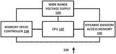
- FIG. 1is a diagram of an information handling system 100 with a wide range power mechanism for over-speed memory design, in accordance with an example embodiment of the present disclosure.
- Information handling system 100includes CPU 102 , wide range voltage supply 104 , dynamic random access memory 106 and memory speed controller 108 , each of which can be implemented in hardware or a suitable combination of hardware and software.
- CPU 102can be an Intel CPU or other suitable processors that are capable of overclocking a memory device.
- CPU 102can include an identifier, such as a K-SKU or other suitable identifiers, which can be used to determine the functional capabilities of CPU 102 .
- CPU 102can also or alternatively include one or more pins that are used to form an electrical connection between external system components and the CPU, such as an STRP pin that can be used to determine CPU 102 functional capabilities.
- Wide range voltage supply 104can be implemented as a stand-alone integrated circuit or in other suitable manners and can provide two or more different voltage levels for devices that it is coupled to, such as CPU 102 and dynamic random access memory 106 .
- wide range voltage supply 104can receive control data from memory speed controller 108 and can adjust the voltage that is output to one or more devices.
- Dynamic random access memory 106can be a memory device with one or more speed setting functions.
- dynamic random access memory 106can support a plurality of different voltage settings, such as 1.2 V and 1.35 V, and a plurality of different speed settings, such as 2133 Mhz, 2667 Mhz, 2933 Mhz, 3200 Mhz, 3600 Mhz and 4200 Mhz, or other suitable settings.
- Memory speed controller 108can be implemented in hardware, such as in an application-specific integrated circuit, a field-programmable gate array or other suitable devices, as one or more algorithms loaded onto and operating on a programmable data processor or in other suitable manners.
- memory speed controller 108can implement one or more algorithms that cause memory speed controller 108 to read data, such as from an STRP pin of a processor, from a data register of a processor or memory device, state data that identifies whether a boot process is in an RTC boot or a cold boot, or other suitable state and/or configuration data, and to generate one or more controls as a function of the state and/or configuration data.
- memory speed controller 108can cause a voltage of wide range voltage supply 104 to be 1.2 V or 1.35 V as a function of the state and/or configuration data, can cause a speed of dynamic random access memory 106 to be 2133 Mhz, 2667 Mhz, 2933 Mhz, 3200 Mhz, 3600 Mhz and 4200 Mhz, or can implement other suitable settings.
- An RTC bootis typically an initial state, when an “RTC battery” is attached for the first time, and where all settings will typically revert back to a default value. There is no specific setting in initial state, and this condition is typically encountered in first boot. For a cold boot, the end-user will typically turn off the system to an “S5—power off state with RTC battery,” and the system will follow a cold boot flow when the power button is pressed afterwards.
- information handling system 100provides voltage and speed control settings for CPU 102 , wide range voltage supply 104 and dynamic random access memory 106 , using memory speed controller 108 to detect system state and system hardware components and to set the voltage and speed in response.
- FIG. 2is a flow chart of an algorithm 200 for controlling an information handling system with a wide range power mechanism for over-speed memory design from a real time clock (RTC) boot, in accordance with an example embodiment of the present disclosure.
- Algorithm 200can be implemented in hardware or a suitable combination of hardware and software.
- Algorithm 200begins at 202 , where an RTC boot occurs. The algorithm then proceeds to 204 .
- a boot settingis implemented for an overclock configuration setting, and the algorithm the proceeds to 206 . Otherwise, a boot setting is implemented for a standard configuration setting, and the algorithm proceeds to 208 .
- a training procedureis implemented.
- the training procedurecan be implemented by rebooting to an overclock configuration setting, or other suitable processes can also or alternatively be used.
- the algorithmthen proceeds to 210 .
- a training procedureis implemented.
- the training procedurecan be implemented by rebooting to a standard configuration setting, or other suitable processes can also or alternatively be used.
- the algorithmthen proceeds to 210 .
- a memorycan support one or more overclock settings.
- the memorycan have a selectable speed setting, where a voltage required for an overclock speed can be higher than a standard voltage setting. If it is determined that the memory can support one or more of the overclock settings, the algorithm proceeds to 212 , otherwise the algorithm then proceeds to 216 .
- the voltage of a voltage supplyis set to a predetermined setting, such as 1.35 Volts or other suitable settlings.
- the voltage supplycan be a wide range voltage supply with a selectable voltage, different dedicated voltage supplies can be used, or other suitable embodiments can also or alternatively be used.
- the algorithmthen proceeds to 214 .
- an XMP profile settingis selected.
- the XMP profile settingcan be stored in a predetermined data memory register associated with a boot process, or in other suitable manners. The algorithm then proceeds to 220 .
- the voltage of a voltage supplyis set to a predetermined setting, such as 1.2 Volts or other suitable settlings.
- the voltage supplycan be a voltage supply with a dedicated voltage, or other suitable embodiments can also or alternatively be used.
- the algorithmthen proceeds to 218 .
- a DRAM profile settingis selected.
- the DRAM profile settingcan be stored in a predetermined data memory register associated with a boot process, or in other suitable manners. The algorithm then proceeds to 220 .
- the systemreboots.
- the algorithmthen proceeds to 222 .
- the operating systemboots.
- algorithm 200controls an information handling system with a wide range power mechanism for over-speed memory design from an RTC boot.
- algorithm 200is shown as a flow chart, a person of skill in the art will recognize that it can also or alternatively be implemented using object-oriented programming, a state diagram, a ladder diagram or in other suitable manners.
- FIG. 3is a flow chart of an algorithm 300 for controlling an information handling system with a wide range power mechanism for over-speed memory design from a cold boot, in accordance with an example embodiment of the present disclosure.
- Algorithm 200can be implemented in hardware or a suitable combination of hardware and software.
- Algorithm 300begins at 302 , where a cold boot occurs. The algorithm then proceeds to 304 .
- a training procedureis implemented.
- the training procedurecan be implemented by rebooting to a stored configuration setting, or other suitable processes can also or alternatively be used.
- the algorithmthen proceeds to 310 .
- a CPU and memorycan support one or more overclock settings.
- the memorycan have a selectable speed setting, where a voltage required for an overclock speed can be higher than a standard voltage setting. If it is determined that the CPU and memory can support one or more of the overclock settings, the algorithm proceeds to 312 , otherwise the algorithm then proceeds to 316 .
- the voltage of a voltage supplyis set to a predetermined setting, such as 1.35 Volts or other suitable settlings.
- the voltage supplycan be a wide range voltage supply with a selectable voltage, different dedicated voltage supplies can be used, or other suitable embodiments can also or alternatively be used.
- the algorithmthen proceeds to 314 .
- an XMP profile settingis selected.
- the XMP profile settingcan be stored in a predetermined data memory register associated with a boot process, or in other suitable manners. The algorithm then proceeds to 320 .
- the voltage of a voltage supplyis set to a predetermined setting, such as 1.2 Volts or other suitable settlings.
- the voltage supplycan be a voltage supply with a dedicated voltage, or other suitable embodiments can also or alternatively be used.
- the algorithmthen proceeds to 318 .
- a DRAM profile settingis selected.
- the DRAM profile settingcan be stored in a predetermined data memory register associated with a boot process, or in other suitable manners. The algorithm then proceeds to 320 .
- the systemreboots.
- the algorithmthen proceeds to 322 .
- the operating systemboots.
- algorithm 300controls an information handling system with a wide range power mechanism for over-speed memory design from a cold boot.
- algorithm 300is shown as a flow chart, a person of skill in the art will recognize that it can also or alternatively be implemented using object-oriented programming, a state diagram, a ladder diagram or in other suitable manners.
- “hardware”can include a combination of discrete components, an integrated circuit, an application-specific integrated circuit, a field programmable gate array, or other suitable hardware.
- “software”can include one or more objects, agents, threads, lines of code, subroutines, separate software applications, two or more lines of code or other suitable software structures operating in two or more software applications, on one or more processors (where a processor includes one or more microcomputers or other suitable data processing units, memory devices, input-output devices, displays, data input devices such as a keyboard or a mouse, peripherals such as printers and speakers, associated drivers, control cards, power sources, network devices, docking station devices, or other suitable devices operating under control of software systems in conjunction with the processor or other devices), or other suitable software structures.
- softwarecan include one or more lines of code or other suitable software structures operating in a general purpose software application, such as an operating system, and one or more lines of code or other suitable software structures operating in a specific purpose software application.
- the term “couple” and its cognate terms, such as “couples” and “coupled,”can include a physical connection (such as a copper conductor), a virtual connection (such as through randomly assigned memory locations of a data memory device), a logical connection (such as through logical gates of a semiconducting device), other suitable connections, or a suitable combination of such connections.
- datacan refer to a suitable structure for using, conveying or storing data, such as a data field, a data buffer, a data message having the data value and sender/receiver address data, a control message having the data value and one or more operators that cause the receiving system or component to perform a function using the data, or other suitable hardware or software components for the electronic processing of data.
- a software systemis a system that operates on a processor to perform predetermined functions in response to predetermined data fields.
- a software systemis typically created as an algorithmic source code by a human programmer, and the source code algorithm is then compiled into a machine language algorithm with the source code algorithm functions, and linked to the specific input/output devices, dynamic link libraries and other specific hardware and software components of a processor, which converts the processor from a general purpose processor into a specific purpose processor.
- This well-known process for implementing an algorithm using a processorshould require no explanation for one of even rudimentary skill in the art.
- a systemcan be defined by the function it performs and the data fields that it performs the function on.
- a NAME systemrefers to a software system that is configured to operate on a processor and to perform the disclosed function on the disclosed data fields.
- a systemcan receive one or more data inputs, such as data fields, user-entered data, control data in response to a user prompt or other suitable data, and can determine an action to take based on an algorithm, such as to proceed to a next algorithmic step if data is received, to repeat a prompt if data is not received, to perform a mathematical operation on two data fields, to sort or display data fields or to perform other suitable well-known algorithmic functions.
- a message system that generates a message that includes a sender address field, a recipient address field and a message fieldwould encompass software operating on a processor that can obtain the sender address field, recipient address field and message field from a suitable system or device of the processor, such as a buffer device or buffer system, can assemble the sender address field, recipient address field and message field into a suitable electronic message format (such as an electronic mail message, a TCP/IP message or any other suitable message format that has a sender address field, a recipient address field and message field), and can transmit the electronic message using electronic messaging systems and devices of the processor over a communications medium, such as a network.
- a suitable electronic message formatsuch as an electronic mail message, a TCP/IP message or any other suitable message format that has a sender address field, a recipient address field and message field
Landscapes
- Engineering & Computer Science (AREA)
- Theoretical Computer Science (AREA)
- Physics & Mathematics (AREA)
- General Engineering & Computer Science (AREA)
- General Physics & Mathematics (AREA)
- Software Systems (AREA)
- Computer Security & Cryptography (AREA)
- Power Sources (AREA)
Abstract
Description
Claims (18)
Priority Applications (2)
| Application Number | Priority Date | Filing Date | Title |
|---|---|---|---|
| US16/883,554US11320885B2 (en) | 2020-05-26 | 2020-05-26 | Wide range power mechanism for over-speed memory design |
| US17/731,967US11755094B2 (en) | 2020-05-26 | 2022-04-28 | Wide range power mechanism for over-speed memory design |
Applications Claiming Priority (1)
| Application Number | Priority Date | Filing Date | Title |
|---|---|---|---|
| US16/883,554US11320885B2 (en) | 2020-05-26 | 2020-05-26 | Wide range power mechanism for over-speed memory design |
Related Child Applications (1)
| Application Number | Title | Priority Date | Filing Date |
|---|---|---|---|
| US17/731,967ContinuationUS11755094B2 (en) | 2020-05-26 | 2022-04-28 | Wide range power mechanism for over-speed memory design |
Publications (2)
| Publication Number | Publication Date |
|---|---|
| US20210373642A1 US20210373642A1 (en) | 2021-12-02 |
| US11320885B2true US11320885B2 (en) | 2022-05-03 |
Family
ID=78706264
Family Applications (2)
| Application Number | Title | Priority Date | Filing Date |
|---|---|---|---|
| US16/883,554Active2040-06-17US11320885B2 (en) | 2020-05-26 | 2020-05-26 | Wide range power mechanism for over-speed memory design |
| US17/731,967ActiveUS11755094B2 (en) | 2020-05-26 | 2022-04-28 | Wide range power mechanism for over-speed memory design |
Family Applications After (1)
| Application Number | Title | Priority Date | Filing Date |
|---|---|---|---|
| US17/731,967ActiveUS11755094B2 (en) | 2020-05-26 | 2022-04-28 | Wide range power mechanism for over-speed memory design |
Country Status (1)
| Country | Link |
|---|---|
| US (2) | US11320885B2 (en) |
Cited By (1)
| Publication number | Priority date | Publication date | Assignee | Title |
|---|---|---|---|---|
| US20240211142A1 (en)* | 2022-12-27 | 2024-06-27 | Advanced Micro Devices, Inc. | Extended Training for Memory |
Families Citing this family (4)
| Publication number | Priority date | Publication date | Assignee | Title |
|---|---|---|---|---|
| US11625276B2 (en)* | 2021-01-08 | 2023-04-11 | Dell Products L.P. | System and method to utilize high bandwidth memory (HBM) |
| US20240143445A1 (en)* | 2022-10-27 | 2024-05-02 | Advanced Micro Devices, Inc. | Stability Testing for Memory Overclocking |
| US12399621B2 (en) | 2022-12-29 | 2025-08-26 | Advanced Micro Devices, Inc. | Automated memory overclocking |
| US12399819B2 (en)* | 2023-03-28 | 2025-08-26 | Micron Technology, Inc. | Memory system characteristic control |
Citations (30)
| Publication number | Priority date | Publication date | Assignee | Title |
|---|---|---|---|---|
| US5862351A (en)* | 1996-11-07 | 1999-01-19 | He; Zhi Qiang | Motherboard with automatic configuration |
| US20030065915A1 (en)* | 2001-10-02 | 2003-04-03 | Chia-Hsing Yu | Method for initializing computer system |
| US6681336B1 (en)* | 1999-06-18 | 2004-01-20 | Kabushiki Kaisha Toshiba | System and method for implementing a user specified processing speed in a computer system and for overriding the user specified processing speed during a startup and shutdown process |
| US20040025069A1 (en)* | 2002-08-01 | 2004-02-05 | Gary Scott P. | Methods and systems for performing dynamic power management via frequency and voltage scaling |
| US20050093524A1 (en)* | 2003-10-31 | 2005-05-05 | Ming-Wei Hsu | Method for CPU power management and bus optimization |
| US20070234075A1 (en)* | 2006-03-29 | 2007-10-04 | Zimmer Vincent J | Methods and apparatus to perform power management in processor systems |
| US20090210565A1 (en)* | 2008-02-14 | 2009-08-20 | Akihito Kohiga | Information Processing Device, and Device Initialization Method in the Information Processing Device |
| US20090265575A1 (en)* | 2008-04-18 | 2009-10-22 | Asustek Computer Inc. | Overclocking module, a computer system and a method for overclocking |
| US20090300343A1 (en)* | 2008-06-03 | 2009-12-03 | Lan Huan Wei | Method and apparatus for changing bios parameters via a hot key |
| US20100115300A1 (en)* | 2008-11-05 | 2010-05-06 | Asustek Computer Inc. | Method and device for adjusting clock frequency and operating voltage of computer system |
| US20100146252A1 (en)* | 2008-12-05 | 2010-06-10 | Micro-Star International Co., Ltd. | Computer motherboard with automatically adjusted hardware parameter value |
| US7761687B2 (en) | 2007-06-26 | 2010-07-20 | International Business Machines Corporation | Ultrascalable petaflop parallel supercomputer |
| US20100199119A1 (en)* | 2009-02-02 | 2010-08-05 | Asustek Computer Inc. | Computer system and method for overclocking the same |
| US7796885B2 (en) | 2002-11-05 | 2010-09-14 | Lightfleet Corporation | Distribution optical elements and compound collecting lenses for broadcast optical interconnect |
| US20100281278A1 (en)* | 2009-04-30 | 2010-11-04 | Asustek Computer Inc. | Computer system and overclock controlling method and program thereof |
| US7917727B2 (en) | 2001-02-14 | 2011-03-29 | Rambus, Inc. | Data processing architectures for packet handling using a SIMD array |
| US20110161706A1 (en)* | 2009-12-28 | 2011-06-30 | Asustek Computer Inc. | Computer system with overclocking function and method |
| US8112625B2 (en) | 1995-02-13 | 2012-02-07 | Intertrust Technologies Corporation | Systems and methods for secure transaction management and electronic rights protection |
| US8193466B2 (en) | 2008-10-24 | 2012-06-05 | Dell Products, Lp | Capacitive input device with removable cover |
| US8625625B2 (en) | 2004-03-10 | 2014-01-07 | Qualcomm Incorporated | High data rate interface apparatus and method |
| US8635358B2 (en) | 2003-09-10 | 2014-01-21 | Qualcomm Incorporated | High data rate interface |
| US20140136823A1 (en)* | 2012-11-15 | 2014-05-15 | Daniel J. Ragland | Enabling A User And/Or Software To Dynamically Control Performance Tuning Of A Processor |
| USRE45097E1 (en)* | 2003-12-18 | 2014-08-26 | Cisco Technology, Inc. | High speed memory and input/output processor subsystem for efficiently allocating and using high-speed memory and slower-speed memory |
| US20150249096A1 (en) | 2012-09-10 | 2015-09-03 | James John Lupino | Three dimension integrated circuits employing thin film transistors |
| US9628365B2 (en) | 1999-10-06 | 2017-04-18 | Benhov Gmbh, Llc | Apparatus for internetworked wireless integrated network sensors (WINS) |
| US20180188769A1 (en)* | 2016-12-30 | 2018-07-05 | Giga-Byte Technology Co.,Ltd. | Memory overclocking method and computer device |
| US20190171270A1 (en)* | 2012-04-19 | 2019-06-06 | Intel Corporation | System, method and apparatus for energy efficiency and energy conservation by configuring power management parameters during run time |
| US20190187766A1 (en)* | 2017-12-15 | 2019-06-20 | Toshiba Client Solutions CO., LTD. | Electric power supply system |
| US10379007B2 (en) | 2015-06-24 | 2019-08-13 | Perrone Robotics, Inc. | Automated robotic test system for automated driving systems |
| US20200192420A1 (en)* | 2018-12-13 | 2020-06-18 | Omer IRSHAD | Computing system with automated video memory overclocking |
Family Cites Families (1)
| Publication number | Priority date | Publication date | Assignee | Title |
|---|---|---|---|---|
| KR20170047468A (en)* | 2015-10-22 | 2017-05-08 | 삼성전자주식회사 | Memory module monitoring memory operation and power management method thereof |
- 2020
- 2020-05-26USUS16/883,554patent/US11320885B2/enactiveActive
- 2022
- 2022-04-28USUS17/731,967patent/US11755094B2/enactiveActive
Patent Citations (31)
| Publication number | Priority date | Publication date | Assignee | Title |
|---|---|---|---|---|
| US8112625B2 (en) | 1995-02-13 | 2012-02-07 | Intertrust Technologies Corporation | Systems and methods for secure transaction management and electronic rights protection |
| US5862351A (en)* | 1996-11-07 | 1999-01-19 | He; Zhi Qiang | Motherboard with automatic configuration |
| US6681336B1 (en)* | 1999-06-18 | 2004-01-20 | Kabushiki Kaisha Toshiba | System and method for implementing a user specified processing speed in a computer system and for overriding the user specified processing speed during a startup and shutdown process |
| US9628365B2 (en) | 1999-10-06 | 2017-04-18 | Benhov Gmbh, Llc | Apparatus for internetworked wireless integrated network sensors (WINS) |
| US7917727B2 (en) | 2001-02-14 | 2011-03-29 | Rambus, Inc. | Data processing architectures for packet handling using a SIMD array |
| US20030065915A1 (en)* | 2001-10-02 | 2003-04-03 | Chia-Hsing Yu | Method for initializing computer system |
| US20040025069A1 (en)* | 2002-08-01 | 2004-02-05 | Gary Scott P. | Methods and systems for performing dynamic power management via frequency and voltage scaling |
| US7796885B2 (en) | 2002-11-05 | 2010-09-14 | Lightfleet Corporation | Distribution optical elements and compound collecting lenses for broadcast optical interconnect |
| US8635358B2 (en) | 2003-09-10 | 2014-01-21 | Qualcomm Incorporated | High data rate interface |
| US20050093524A1 (en)* | 2003-10-31 | 2005-05-05 | Ming-Wei Hsu | Method for CPU power management and bus optimization |
| USRE45097E1 (en)* | 2003-12-18 | 2014-08-26 | Cisco Technology, Inc. | High speed memory and input/output processor subsystem for efficiently allocating and using high-speed memory and slower-speed memory |
| US8625625B2 (en) | 2004-03-10 | 2014-01-07 | Qualcomm Incorporated | High data rate interface apparatus and method |
| US20070234075A1 (en)* | 2006-03-29 | 2007-10-04 | Zimmer Vincent J | Methods and apparatus to perform power management in processor systems |
| US7761687B2 (en) | 2007-06-26 | 2010-07-20 | International Business Machines Corporation | Ultrascalable petaflop parallel supercomputer |
| US20090210565A1 (en)* | 2008-02-14 | 2009-08-20 | Akihito Kohiga | Information Processing Device, and Device Initialization Method in the Information Processing Device |
| US20090265575A1 (en)* | 2008-04-18 | 2009-10-22 | Asustek Computer Inc. | Overclocking module, a computer system and a method for overclocking |
| US20090300343A1 (en)* | 2008-06-03 | 2009-12-03 | Lan Huan Wei | Method and apparatus for changing bios parameters via a hot key |
| US8193466B2 (en) | 2008-10-24 | 2012-06-05 | Dell Products, Lp | Capacitive input device with removable cover |
| US8987624B2 (en) | 2008-10-24 | 2015-03-24 | Dell Products, Lp | Capacitive input device with removable cover |
| US20100115300A1 (en)* | 2008-11-05 | 2010-05-06 | Asustek Computer Inc. | Method and device for adjusting clock frequency and operating voltage of computer system |
| US20100146252A1 (en)* | 2008-12-05 | 2010-06-10 | Micro-Star International Co., Ltd. | Computer motherboard with automatically adjusted hardware parameter value |
| US20100199119A1 (en)* | 2009-02-02 | 2010-08-05 | Asustek Computer Inc. | Computer system and method for overclocking the same |
| US20100281278A1 (en)* | 2009-04-30 | 2010-11-04 | Asustek Computer Inc. | Computer system and overclock controlling method and program thereof |
| US20110161706A1 (en)* | 2009-12-28 | 2011-06-30 | Asustek Computer Inc. | Computer system with overclocking function and method |
| US20190171270A1 (en)* | 2012-04-19 | 2019-06-06 | Intel Corporation | System, method and apparatus for energy efficiency and energy conservation by configuring power management parameters during run time |
| US20150249096A1 (en) | 2012-09-10 | 2015-09-03 | James John Lupino | Three dimension integrated circuits employing thin film transistors |
| US20140136823A1 (en)* | 2012-11-15 | 2014-05-15 | Daniel J. Ragland | Enabling A User And/Or Software To Dynamically Control Performance Tuning Of A Processor |
| US10379007B2 (en) | 2015-06-24 | 2019-08-13 | Perrone Robotics, Inc. | Automated robotic test system for automated driving systems |
| US20180188769A1 (en)* | 2016-12-30 | 2018-07-05 | Giga-Byte Technology Co.,Ltd. | Memory overclocking method and computer device |
| US20190187766A1 (en)* | 2017-12-15 | 2019-06-20 | Toshiba Client Solutions CO., LTD. | Electric power supply system |
| US20200192420A1 (en)* | 2018-12-13 | 2020-06-18 | Omer IRSHAD | Computing system with automated video memory overclocking |
Cited By (2)
| Publication number | Priority date | Publication date | Assignee | Title |
|---|---|---|---|---|
| US20240211142A1 (en)* | 2022-12-27 | 2024-06-27 | Advanced Micro Devices, Inc. | Extended Training for Memory |
| US12422990B2 (en)* | 2022-12-27 | 2025-09-23 | Advanced Micro Devices, Inc. | Extended training for memory |
Also Published As
| Publication number | Publication date |
|---|---|
| US20210373642A1 (en) | 2021-12-02 |
| US20220253123A1 (en) | 2022-08-11 |
| US11755094B2 (en) | 2023-09-12 |
Similar Documents
| Publication | Publication Date | Title |
|---|---|---|
| US11755094B2 (en) | Wide range power mechanism for over-speed memory design | |
| US6237103B1 (en) | Power sequencing in a data processing system | |
| JP6864718B2 (en) | Hybrid power supply system and method | |
| US8935558B2 (en) | Overclocking module, a computer system and a method for overclocking | |
| US20240264824A1 (en) | Method of updating firmware of computer | |
| US20100125726A1 (en) | Thin client host wakeup method and thin client host | |
| US20200341526A1 (en) | System and method for managing power to server | |
| US9520163B2 (en) | Regulator circuit and semiconductor memory apparatus having the same | |
| US10853085B2 (en) | Adjustable performance boot system | |
| EP0430219A2 (en) | Method and system for controlling a resume process in a computer unit capable of connecting an expansion unit | |
| US6393558B1 (en) | Peripheral component interconnect (PCI) card for selectively processing a PCI bus reset signal and method for resetting the PCI card | |
| CN112382334A (en) | Testing device and testing method for mobile memory | |
| US11061849B2 (en) | Adaptive transmitter preset mechanism in PCIe link equalization procedure | |
| US7200451B2 (en) | Method for consistent on/off object to control radios and other interfaces | |
| US11842057B2 (en) | Seamless creation of raid arrays with optimized boot time | |
| KR100388961B1 (en) | data restoring control device of the flash ROM in the information processing system | |
| US10838707B2 (en) | Runtime update of intel server platform services' node manager settings in bios EEPROM | |
| US20210349516A1 (en) | Energy saving device and method for saving energy in data center | |
| US10732699B2 (en) | Redundancy in distribution of voltage-frequency scaling parameters | |
| CN111694300A (en) | Automatic configuration method and device for control panel input and output ports | |
| US20240086222A1 (en) | Method to manage a hyper-converged infrastructure with a desired state model | |
| US12117897B2 (en) | System and method for managing conditions impacting power supplies of data processing systems | |
| CN112394769B (en) | Motherboards that support different types of memory | |
| CN115440295B (en) | Device and method for testing data loading capacity of eMMC chip | |
| TWI391825B (en) | Processing module, operation system and processing method utilizing the same |
Legal Events
| Date | Code | Title | Description |
|---|---|---|---|
| AS | Assignment | Owner name:DELL PRODUCTS L.P., TEXAS Free format text:ASSIGNMENT OF ASSIGNORS INTEREST;ASSIGNORS:WANG, CHUNGE-WEI;LIN, CHIHCHUNG;CHU, TSE-AN-;AND OTHERS;SIGNING DATES FROM 20200522 TO 20200525;REEL/FRAME:052752/0829 | |
| FEPP | Fee payment procedure | Free format text:ENTITY STATUS SET TO UNDISCOUNTED (ORIGINAL EVENT CODE: BIG.); ENTITY STATUS OF PATENT OWNER: LARGE ENTITY | |
| AS | Assignment | Owner name:CREDIT SUISSE AG, CAYMAN ISLANDS BRANCH, NORTH CAROLINA Free format text:SECURITY AGREEMENT;ASSIGNORS:DELL PRODUCTS L.P.;EMC IP HOLDING COMPANY LLC;REEL/FRAME:053531/0108 Effective date:20200818 | |
| AS | Assignment | Owner name:THE BANK OF NEW YORK MELLON TRUST COMPANY, N.A., AS NOTES COLLATERAL AGENT, TEXAS Free format text:SECURITY INTEREST;ASSIGNORS:DELL PRODUCTS L.P.;EMC IP HOLDING COMPANY LLC;REEL/FRAME:053578/0183 Effective date:20200817 Owner name:THE BANK OF NEW YORK MELLON TRUST COMPANY, N.A., AS NOTES COLLATERAL AGENT, TEXAS Free format text:SECURITY INTEREST;ASSIGNORS:DELL PRODUCTS L.P.;EMC IP HOLDING COMPANY LLC;REEL/FRAME:053574/0221 Effective date:20200817 Owner name:THE BANK OF NEW YORK MELLON TRUST COMPANY, N.A., AS NOTES COLLATERAL AGENT, TEXAS Free format text:SECURITY INTEREST;ASSIGNORS:DELL PRODUCTS L.P.;EMC IP HOLDING COMPANY LLC;REEL/FRAME:053573/0535 Effective date:20200817 | |
| STPP | Information on status: patent application and granting procedure in general | Free format text:FINAL REJECTION MAILED | |
| AS | Assignment | Owner name:EMC IP HOLDING COMPANY LLC, TEXAS Free format text:RELEASE OF SECURITY INTEREST AT REEL 053531 FRAME 0108;ASSIGNOR:CREDIT SUISSE AG, CAYMAN ISLANDS BRANCH;REEL/FRAME:058001/0371 Effective date:20211101 Owner name:DELL PRODUCTS L.P., TEXAS Free format text:RELEASE OF SECURITY INTEREST AT REEL 053531 FRAME 0108;ASSIGNOR:CREDIT SUISSE AG, CAYMAN ISLANDS BRANCH;REEL/FRAME:058001/0371 Effective date:20211101 | |
| STPP | Information on status: patent application and granting procedure in general | Free format text:RESPONSE AFTER FINAL ACTION FORWARDED TO EXAMINER | |
| STPP | Information on status: patent application and granting procedure in general | Free format text:NOTICE OF ALLOWANCE MAILED -- APPLICATION RECEIVED IN OFFICE OF PUBLICATIONS | |
| STPP | Information on status: patent application and granting procedure in general | Free format text:PUBLICATIONS -- ISSUE FEE PAYMENT VERIFIED | |
| STCF | Information on status: patent grant | Free format text:PATENTED CASE | |
| AS | Assignment | Owner name:EMC IP HOLDING COMPANY LLC, TEXAS Free format text:RELEASE OF SECURITY INTEREST IN PATENTS PREVIOUSLY RECORDED AT REEL/FRAME (053574/0221);ASSIGNOR:THE BANK OF NEW YORK MELLON TRUST COMPANY, N.A., AS NOTES COLLATERAL AGENT;REEL/FRAME:060333/0001 Effective date:20220329 Owner name:DELL PRODUCTS L.P., TEXAS Free format text:RELEASE OF SECURITY INTEREST IN PATENTS PREVIOUSLY RECORDED AT REEL/FRAME (053574/0221);ASSIGNOR:THE BANK OF NEW YORK MELLON TRUST COMPANY, N.A., AS NOTES COLLATERAL AGENT;REEL/FRAME:060333/0001 Effective date:20220329 Owner name:EMC IP HOLDING COMPANY LLC, TEXAS Free format text:RELEASE OF SECURITY INTEREST IN PATENTS PREVIOUSLY RECORDED AT REEL/FRAME (053578/0183);ASSIGNOR:THE BANK OF NEW YORK MELLON TRUST COMPANY, N.A., AS NOTES COLLATERAL AGENT;REEL/FRAME:060332/0864 Effective date:20220329 Owner name:DELL PRODUCTS L.P., TEXAS Free format text:RELEASE OF SECURITY INTEREST IN PATENTS PREVIOUSLY RECORDED AT REEL/FRAME (053578/0183);ASSIGNOR:THE BANK OF NEW YORK MELLON TRUST COMPANY, N.A., AS NOTES COLLATERAL AGENT;REEL/FRAME:060332/0864 Effective date:20220329 Owner name:EMC IP HOLDING COMPANY LLC, TEXAS Free format text:RELEASE OF SECURITY INTEREST IN PATENTS PREVIOUSLY RECORDED AT REEL/FRAME (053573/0535);ASSIGNOR:THE BANK OF NEW YORK MELLON TRUST COMPANY, N.A., AS NOTES COLLATERAL AGENT;REEL/FRAME:060333/0106 Effective date:20220329 Owner name:DELL PRODUCTS L.P., TEXAS Free format text:RELEASE OF SECURITY INTEREST IN PATENTS PREVIOUSLY RECORDED AT REEL/FRAME (053573/0535);ASSIGNOR:THE BANK OF NEW YORK MELLON TRUST COMPANY, N.A., AS NOTES COLLATERAL AGENT;REEL/FRAME:060333/0106 Effective date:20220329 |