US11315954B2 - Semiconductor device and manufacturing method thereof - Google Patents
Semiconductor device and manufacturing method thereofDownload PDFInfo
- Publication number
- US11315954B2 US11315954B2US16/130,550US201816130550AUS11315954B2US 11315954 B2US11315954 B2US 11315954B2US 201816130550 AUS201816130550 AUS 201816130550AUS 11315954 B2US11315954 B2US 11315954B2
- Authority
- US
- United States
- Prior art keywords
- transistor
- layer
- oxide semiconductor
- electrode layer
- electrode
- Prior art date
- Legal status (The legal status is an assumption and is not a legal conclusion. Google has not performed a legal analysis and makes no representation as to the accuracy of the status listed.)
- Active
Links
Images


Classifications
- H01L27/1225—
- H—ELECTRICITY
- H10—SEMICONDUCTOR DEVICES; ELECTRIC SOLID-STATE DEVICES NOT OTHERWISE PROVIDED FOR
- H10D—INORGANIC ELECTRIC SEMICONDUCTOR DEVICES
- H10D86/00—Integrated devices formed in or on insulating or conducting substrates, e.g. formed in silicon-on-insulator [SOI] substrates or on stainless steel or glass substrates
- H10D86/40—Integrated devices formed in or on insulating or conducting substrates, e.g. formed in silicon-on-insulator [SOI] substrates or on stainless steel or glass substrates characterised by multiple TFTs
- H10D86/60—Integrated devices formed in or on insulating or conducting substrates, e.g. formed in silicon-on-insulator [SOI] substrates or on stainless steel or glass substrates characterised by multiple TFTs wherein the TFTs are in active matrices
- H01L27/0883—
- H01L27/1251—
- H01L27/127—
- H01L27/1288—
- H01L29/045—
- H01L29/24—
- H01L29/7869—
- H01L29/78693—
- H01L29/78696—
- H—ELECTRICITY
- H10—SEMICONDUCTOR DEVICES; ELECTRIC SOLID-STATE DEVICES NOT OTHERWISE PROVIDED FOR
- H10D—INORGANIC ELECTRIC SEMICONDUCTOR DEVICES
- H10D30/00—Field-effect transistors [FET]
- H10D30/60—Insulated-gate field-effect transistors [IGFET]
- H10D30/67—Thin-film transistors [TFT]
- H10D30/6729—Thin-film transistors [TFT] characterised by the electrodes
- H10D30/673—Thin-film transistors [TFT] characterised by the electrodes characterised by the shapes, relative sizes or dispositions of the gate electrodes
- H10D30/6732—Bottom-gate only TFTs
- H—ELECTRICITY
- H10—SEMICONDUCTOR DEVICES; ELECTRIC SOLID-STATE DEVICES NOT OTHERWISE PROVIDED FOR
- H10D—INORGANIC ELECTRIC SEMICONDUCTOR DEVICES
- H10D30/00—Field-effect transistors [FET]
- H10D30/60—Insulated-gate field-effect transistors [IGFET]
- H10D30/67—Thin-film transistors [TFT]
- H10D30/6729—Thin-film transistors [TFT] characterised by the electrodes
- H10D30/673—Thin-film transistors [TFT] characterised by the electrodes characterised by the shapes, relative sizes or dispositions of the gate electrodes
- H10D30/6733—Multi-gate TFTs
- H10D30/6734—Multi-gate TFTs having gate electrodes arranged on both top and bottom sides of the channel, e.g. dual-gate TFTs
- H—ELECTRICITY
- H10—SEMICONDUCTOR DEVICES; ELECTRIC SOLID-STATE DEVICES NOT OTHERWISE PROVIDED FOR
- H10D—INORGANIC ELECTRIC SEMICONDUCTOR DEVICES
- H10D30/00—Field-effect transistors [FET]
- H10D30/60—Insulated-gate field-effect transistors [IGFET]
- H10D30/67—Thin-film transistors [TFT]
- H10D30/674—Thin-film transistors [TFT] characterised by the active materials
- H10D30/6741—Group IV materials, e.g. germanium or silicon carbide
- H10D30/6743—Silicon
- H10D30/6745—Polycrystalline or microcrystalline silicon
- H—ELECTRICITY
- H10—SEMICONDUCTOR DEVICES; ELECTRIC SOLID-STATE DEVICES NOT OTHERWISE PROVIDED FOR
- H10D—INORGANIC ELECTRIC SEMICONDUCTOR DEVICES
- H10D30/00—Field-effect transistors [FET]
- H10D30/60—Insulated-gate field-effect transistors [IGFET]
- H10D30/67—Thin-film transistors [TFT]
- H10D30/674—Thin-film transistors [TFT] characterised by the active materials
- H10D30/6741—Group IV materials, e.g. germanium or silicon carbide
- H10D30/6743—Silicon
- H10D30/6746—Amorphous silicon
- H—ELECTRICITY
- H10—SEMICONDUCTOR DEVICES; ELECTRIC SOLID-STATE DEVICES NOT OTHERWISE PROVIDED FOR
- H10D—INORGANIC ELECTRIC SEMICONDUCTOR DEVICES
- H10D30/00—Field-effect transistors [FET]
- H10D30/60—Insulated-gate field-effect transistors [IGFET]
- H10D30/67—Thin-film transistors [TFT]
- H10D30/674—Thin-film transistors [TFT] characterised by the active materials
- H10D30/6755—Oxide semiconductors, e.g. zinc oxide, copper aluminium oxide or cadmium stannate
- H10D30/6756—Amorphous oxide semiconductors
- H—ELECTRICITY
- H10—SEMICONDUCTOR DEVICES; ELECTRIC SOLID-STATE DEVICES NOT OTHERWISE PROVIDED FOR
- H10D—INORGANIC ELECTRIC SEMICONDUCTOR DEVICES
- H10D30/00—Field-effect transistors [FET]
- H10D30/60—Insulated-gate field-effect transistors [IGFET]
- H10D30/67—Thin-film transistors [TFT]
- H10D30/6757—Thin-film transistors [TFT] characterised by the structure of the channel, e.g. transverse or longitudinal shape or doping profile
- H—ELECTRICITY
- H10—SEMICONDUCTOR DEVICES; ELECTRIC SOLID-STATE DEVICES NOT OTHERWISE PROVIDED FOR
- H10D—INORGANIC ELECTRIC SEMICONDUCTOR DEVICES
- H10D62/00—Semiconductor bodies, or regions thereof, of devices having potential barriers
- H10D62/40—Crystalline structures
- H10D62/405—Orientations of crystalline planes
- H—ELECTRICITY
- H10—SEMICONDUCTOR DEVICES; ELECTRIC SOLID-STATE DEVICES NOT OTHERWISE PROVIDED FOR
- H10D—INORGANIC ELECTRIC SEMICONDUCTOR DEVICES
- H10D62/00—Semiconductor bodies, or regions thereof, of devices having potential barriers
- H10D62/80—Semiconductor bodies, or regions thereof, of devices having potential barriers characterised by the materials
- H—ELECTRICITY
- H10—SEMICONDUCTOR DEVICES; ELECTRIC SOLID-STATE DEVICES NOT OTHERWISE PROVIDED FOR
- H10D—INORGANIC ELECTRIC SEMICONDUCTOR DEVICES
- H10D84/00—Integrated devices formed in or on semiconductor substrates that comprise only semiconducting layers, e.g. on Si wafers or on GaAs-on-Si wafers
- H10D84/80—Integrated devices formed in or on semiconductor substrates that comprise only semiconducting layers, e.g. on Si wafers or on GaAs-on-Si wafers characterised by the integration of at least one component covered by groups H10D12/00 or H10D30/00, e.g. integration of IGFETs
- H10D84/82—Integrated devices formed in or on semiconductor substrates that comprise only semiconducting layers, e.g. on Si wafers or on GaAs-on-Si wafers characterised by the integration of at least one component covered by groups H10D12/00 or H10D30/00, e.g. integration of IGFETs of only field-effect components
- H10D84/83—Integrated devices formed in or on semiconductor substrates that comprise only semiconducting layers, e.g. on Si wafers or on GaAs-on-Si wafers characterised by the integration of at least one component covered by groups H10D12/00 or H10D30/00, e.g. integration of IGFETs of only field-effect components of only insulated-gate FETs [IGFET]
- H10D84/84—Combinations of enhancement-mode IGFETs and depletion-mode IGFETs
- H—ELECTRICITY
- H10—SEMICONDUCTOR DEVICES; ELECTRIC SOLID-STATE DEVICES NOT OTHERWISE PROVIDED FOR
- H10D—INORGANIC ELECTRIC SEMICONDUCTOR DEVICES
- H10D86/00—Integrated devices formed in or on insulating or conducting substrates, e.g. formed in silicon-on-insulator [SOI] substrates or on stainless steel or glass substrates
- H10D86/01—Manufacture or treatment
- H10D86/021—Manufacture or treatment of multiple TFTs
- H10D86/0221—Manufacture or treatment of multiple TFTs comprising manufacture, treatment or patterning of TFT semiconductor bodies
- H—ELECTRICITY
- H10—SEMICONDUCTOR DEVICES; ELECTRIC SOLID-STATE DEVICES NOT OTHERWISE PROVIDED FOR
- H10D—INORGANIC ELECTRIC SEMICONDUCTOR DEVICES
- H10D86/00—Integrated devices formed in or on insulating or conducting substrates, e.g. formed in silicon-on-insulator [SOI] substrates or on stainless steel or glass substrates
- H10D86/01—Manufacture or treatment
- H10D86/021—Manufacture or treatment of multiple TFTs
- H10D86/0231—Manufacture or treatment of multiple TFTs using masks, e.g. half-tone masks
- H—ELECTRICITY
- H10—SEMICONDUCTOR DEVICES; ELECTRIC SOLID-STATE DEVICES NOT OTHERWISE PROVIDED FOR
- H10D—INORGANIC ELECTRIC SEMICONDUCTOR DEVICES
- H10D86/00—Integrated devices formed in or on insulating or conducting substrates, e.g. formed in silicon-on-insulator [SOI] substrates or on stainless steel or glass substrates
- H10D86/40—Integrated devices formed in or on insulating or conducting substrates, e.g. formed in silicon-on-insulator [SOI] substrates or on stainless steel or glass substrates characterised by multiple TFTs
- H10D86/421—Integrated devices formed in or on insulating or conducting substrates, e.g. formed in silicon-on-insulator [SOI] substrates or on stainless steel or glass substrates characterised by multiple TFTs having a particular composition, shape or crystalline structure of the active layer
- H10D86/423—Integrated devices formed in or on insulating or conducting substrates, e.g. formed in silicon-on-insulator [SOI] substrates or on stainless steel or glass substrates characterised by multiple TFTs having a particular composition, shape or crystalline structure of the active layer comprising semiconductor materials not belonging to the Group IV, e.g. InGaZnO
- H—ELECTRICITY
- H10—SEMICONDUCTOR DEVICES; ELECTRIC SOLID-STATE DEVICES NOT OTHERWISE PROVIDED FOR
- H10D—INORGANIC ELECTRIC SEMICONDUCTOR DEVICES
- H10D86/00—Integrated devices formed in or on insulating or conducting substrates, e.g. formed in silicon-on-insulator [SOI] substrates or on stainless steel or glass substrates
- H10D86/40—Integrated devices formed in or on insulating or conducting substrates, e.g. formed in silicon-on-insulator [SOI] substrates or on stainless steel or glass substrates characterised by multiple TFTs
- H10D86/471—Integrated devices formed in or on insulating or conducting substrates, e.g. formed in silicon-on-insulator [SOI] substrates or on stainless steel or glass substrates characterised by multiple TFTs having different architectures, e.g. having both top-gate and bottom-gate TFTs
- H—ELECTRICITY
- H01—ELECTRIC ELEMENTS
- H01L—SEMICONDUCTOR DEVICES NOT COVERED BY CLASS H10
- H01L21/00—Processes or apparatus adapted for the manufacture or treatment of semiconductor or solid state devices or of parts thereof
- H01L21/02—Manufacture or treatment of semiconductor devices or of parts thereof
- H01L21/02104—Forming layers
- H01L21/02365—Forming inorganic semiconducting materials on a substrate
- H01L21/02518—Deposited layers
- H01L21/02587—Structure
- H01L21/0259—Microstructure
- H01L21/02603—Nanowires
- H01L29/04—
- H01L29/4908—
- H—ELECTRICITY
- H01—ELECTRIC ELEMENTS
- H01L—SEMICONDUCTOR DEVICES NOT COVERED BY CLASS H10
- H01L2924/00—Indexing scheme for arrangements or methods for connecting or disconnecting semiconductor or solid-state bodies as covered by H01L24/00
- H01L2924/10—Details of semiconductor or other solid state devices to be connected
- H01L2924/11—Device type
- H01L2924/13—Discrete devices, e.g. 3 terminal devices
- H01L2924/1304—Transistor
- H01L2924/1306—Field-effect transistor [FET]
- H01L2924/13069—Thin film transistor [TFT]
- H—ELECTRICITY
- H10—SEMICONDUCTOR DEVICES; ELECTRIC SOLID-STATE DEVICES NOT OTHERWISE PROVIDED FOR
- H10D—INORGANIC ELECTRIC SEMICONDUCTOR DEVICES
- H10D30/00—Field-effect transistors [FET]
- H10D30/60—Insulated-gate field-effect transistors [IGFET]
- H10D30/67—Thin-film transistors [TFT]
- H10D30/6729—Thin-film transistors [TFT] characterised by the electrodes
- H10D30/6737—Thin-film transistors [TFT] characterised by the electrodes characterised by the electrode materials
- H10D30/6739—Conductor-insulator-semiconductor electrodes
- H—ELECTRICITY
- H10—SEMICONDUCTOR DEVICES; ELECTRIC SOLID-STATE DEVICES NOT OTHERWISE PROVIDED FOR
- H10D—INORGANIC ELECTRIC SEMICONDUCTOR DEVICES
- H10D62/00—Semiconductor bodies, or regions thereof, of devices having potential barriers
- H10D62/40—Crystalline structures
Definitions
- the present inventionrelates to a semiconductor device including a transistor.
- semiconductor device in this specificationrefers to any device that can function by utilizing semiconductor characteristics, and semiconductor elements and circuits, electro-optic devices including semiconductor elements and circuits, and electronic devices including semiconductor elements and circuits are all semiconductor devices.
- a transistoris used for a semiconductor device typified by a liquid crystal television.
- a semiconductor thin film that can be applied to the transistorsa silicon-based semiconductor material is known, and an oxide semiconductor attracts attention as another material.
- a transistoris manufactured mainly using a semiconductor material such as amorphous silicon or polycrystalline silicon.
- a transistor formed using amorphous siliconhas low field-effect mobility, but such a transistor can be formed over a glass substrate with a larger area.
- a transistor formed using crystalline siliconhas high field-effect mobility, but a crystallization step such as laser annealing is necessary and such a transistor is not always suitable for a larger glass substrate.
- oxide semiconductorAs a material of the oxide semiconductor, zinc oxide and a material containing zinc oxide as its component are known. Further, thin film transistors formed using an amorphous oxide (oxide semiconductor) having an electron carrier concentration of less than 10 18 /cm 3 are disclosed (Patent Documents 1 to 3).
- an active matrix semiconductor devicetypified by a liquid crystal display device towards a larger screen, e.g., a 60-inch diagonal screen
- the development of an active matrix semiconductor deviceis aimed even at a screen size of a diagonal of 120 inches or more.
- a trend in resolution of a screenis toward higher definition, e.g., high-definition (HD) image quality (1366 ⁇ 768) or full high-definition (FHD) image quality (1920 ⁇ 1080), and prompt development of a so-called 4K Digital Cinema display device, which has a resolution of 3840 ⁇ 2048 or 4096 ⁇ 2160, is also pushed.
- HDhigh-definition
- FHDfull high-definition
- a display deviceAs a display device has a higher definition, the number of pixels needed for it is significantly increased. As a result, writing time for one pixel is shortened, and thus a transistor is required to have high speed operation characteristics, large on current, and the like. In the meantime, a problem of energy depletion in recent years has caused demand for a display device whose power consumption is suppressed. Therefore, a transistor is also required to have low off-state current and suppressed unnecessary leakage current.
- Patent Document 1Japanese Published Patent Application No. 2006-165527
- Patent Document 2Japanese Published Patent Application No. 2006-165528
- Patent Document 3Japanese Published Patent Application No. 2006-165529
- a transistor using an oxide semiconductorhas higher field-effect mobility than a transistor using amorphous silicon.
- a transistor using an oxide semiconductorhas lower field-effect mobility than a transistor using polycrystalline silicon, so that field-effect mobility of a transistor using an oxide semiconductor is required to be further improved.
- a difference from the stoichiometric composition in an oxide semiconductorarises in a formation process.
- electrical conductivity of an oxide semiconductoris changed due to excess and deficiency of oxygen.
- hydrogen that enters the oxide semiconductor thin film during the formation of the thin filmforms an oxygen (O)-hydrogen (H) bond and serves as an electron donor, which is a factor of changing electric conductivity.
- the O—H bondis a bond having polarity; and thus, the O—H bond might cause variation in characteristics of an active device such as a transistor formed using an oxide semiconductor.
- the oxide semiconductoris substantially n-type, and the on/off ratio of the transistors disclosed in the above patent documents is only 10 3 . Such a low on/off ratio of the transistor is due to large off-state current.
- an object of the present inventionis to provide a semiconductor device in which transistors with different characteristics, specifically, a transistor with excellent dynamic characteristics (on characteristics or frequency characteristics (referred to as f characteristics)) and a transistor having a reduced off-state current, are provided over one substrate. Further, another object is to provide a simple method for manufacturing the semiconductor device.
- an oxide semiconductor layer which is intrinsic or substantially intrinsic and includes a crystalline region in a surface portionis focused.
- a semiconductor from which an impurity which is to be an electron donor (donor) from an oxide semiconductor is removed and which has a larger energy gap than a silicon semiconductorcan be used as a semiconductor which is intrinsic or substantially intrinsic.
- the electric characteristics of transistorsis controlled by controlling the potential of a pair of conductive films which are provided on opposite sides form each other with respect to the oxide semiconductor layer, each with an insulating film arranged therebetween, so that the position of a channel formed in the oxide semiconductor layer is determined.
- One embodiment of the present inventionis a semiconductor device in which a transistor with excellent dynamic characteristics and a transistor with stable electric characteristics (e.g., an extremely reduced off-state current) are used over one substrate.
- an embodiment of the present inventionis a semiconductor from which an impurity which is to be an electron donor (donor) from an oxide semiconductor is removed and which has a larger energy gap than a silicon semiconductor can be used.
- an oxide semiconductor layerwhich is intrinsic or substantially intrinsic and includes a crystalline region in a surface portion of the oxide semiconductor layer is formed.
- a plurality of transistorshaving a structure in which conductive films which are provided on opposite sides from each other with respect to the oxide semiconductor layer, each with an insulating film arranged therebetween is provided over one substrate.
- an embodiment of the present inventionis a semiconductor device including a first electrode layer, a first insulating film over the first electrode layer, an oxide semiconductor layer including a crystalline region in a surface portion of the oxide semiconductor layer, over the first insulating film, a second electrode layer and a third electrode layer over the first electrode layer and in contact with the oxide semiconductor layer, the second electrode layer having an end portion overlapping with the first electrode layer, and the third electrode layer having an end portion overlapping with the first electrode layer, a second insulating film including an oxide insulating film in contact with the second electrode layer, the third electrode layer, and the oxide semiconductor layer, and a fourth electrode layer overlapping with the first electrode layer and the oxide semiconductor layer, over the second insulating film.
- the semiconductor deviceincludes a plurality of transistors in which an energy gap of an oxide semiconductor used in the oxide semiconductor layer is greater than or equal to 2 eV.
- An embodiment of the present inventionis an inverter circuit which includes the above-described semiconductor device including a depression transistor and an enhancement transistor.
- An embodiment of the present inventionis includes a display device which includes the above-described semiconductor device including a pixel portion and a driver circuit portion which drives the pixel portion.
- An embodiment of the present inventionis a driving method using the first electrode layer as a main gate electrode in at least one transistor and the fourth electrode layer as a main gate electrode in the other transistors in the above-described semiconductor device.
- An embodiment of the present inventionis a driving method using the fourth electrode layer as a main gate electrode in the depletion transistor and the fourth electrode layer as a main gate electrode in the enhancement transistor in the above-described inverter circuit.
- An embodiment of the present inventionis a driving method using the first electrode layer as a main gate electrode in at least one transistor included in the pixel portion and the fourth electrode layer as a main gate electrode in at least one transistor included in the driver circuit portion in the above-described display device.
- An embodiment of the present inventionis a manufacturing method of a semiconductor device including the steps of forming a first electrode layer, forming a first insulating film over the first electrode layer, forming an oxide semiconductor layer over the first insulating film, performing dehydration or dehydrogenation on the oxide semiconductor layer so that a crystalline region is formed in a surface portion of the oxide semiconductor layer, forming a second electrode layer and a third electrode layer over the first electrode layer and in contact with the oxide semiconductor layer, the second electrode layer having an end portion overlapping with the first electrode layer, and the third electrode layer having an end portion overlapping with the first electrode layer, forming a second insulating film including an oxide insulating film in contact with the second electrode layer, the third electrode layer, and the oxide semiconductor layer, and forming a fourth electrode layer overlapping with the first electrode layer and the oxide semiconductor layer, over the second insulating film.
- the above-described semiconductor deviceincludes a plurality of transistors over one substrate in which an energy gap of an oxide semiconductor used in the oxide semiconductor layer is greater than or
- an EL layerrefers to a layer provided between a pair of electrodes in a light-emitting element.
- a light-emitting layer containing an organic compound that is a light-emitting substance which is interposed between electrodesis an embodiment of the EL layer.
- a light-emitting devicerefers to an image display device, a light-emitting device, or a light source (including a lighting device).
- the light-emitting deviceincludes any of the following modules in its category: a module in which a connector such as a flexible printed circuit (FPC), a tape automated bonding (TAB) tape, or a tape carrier package (TCP) is attached to a light-emitting device; a module having a TAB tape or a TCP provided with a printed wiring board at the end thereof; and a module having an integrated circuit (IC) directly mounted over a substrate over which a light-emitting element is formed by a chip on glass (COG) method.
- a connectorsuch as a flexible printed circuit (FPC), a tape automated bonding (TAB) tape, or a tape carrier package (TCP) is attached to a light-emitting device
- TABtape automated bonding
- TCPtape carrier package
- COGchip on glass
- a crystalline region included in an oxide semiconductor layeris used as a channel formation region, whereby operation speed of the circuit included in a semiconductor device can be increased.
- a circuitis formed using a transistor in which a purified oxide semiconductor is used, whereby operation of the circuit included in a semiconductor device can be stabilized.
- off-state currentreduced to 1 ⁇ 10 ⁇ 13 A or lower, whereby a storage capacitor included in a semiconductor device can be reduced in size or in number.
- a semiconductor device including transistors with different characteristics over one substratecan be provided. Furthermore, the semiconductor device can be manufactured by a simple method.
- FIGS. 1A to 1Eeach illustrate a manufacturing method of a semiconductor device according to an embodiment
- FIG. 2illustrates a semiconductor device according to an embodiment
- FIGS. 3A to 3Ceach illustrate an inverter circuit according to an embodiment
- FIGS. 4A to 4Ceach illustrate a shift register according to an embodiment
- FIGS. 5A and 5Beach illustrate a pulse output circuit according to an embodiment
- FIGS. 6A to 6Deach illustrate a pulse output circuit according to an embodiment
- FIGS. 7A to 7Deach illustrate a pulse output circuit according to an embodiment
- FIGS. 8A and 8Beach illustrate a timing chart according to an embodiment
- FIGS. 9A and 9Bare block diagrams of display devices according to an embodiment
- FIGS. 10A and 10Beach illustrate a driver circuit of a display device according to an embodiment
- FIGS. 11 A 1 and 11 A 2are cross-sectional views and FIG. 11B is a plan view each illustrating an embodiment of the present invention
- FIG. 12is a cross-sectional view illustrating an embodiment of the present invention.
- FIG. 13is a cross-sectional view illustrating an embodiment of the present invention.
- FIG. 14shows an equivalent circuit of a pixel in a semiconductor device
- FIGS. 15A to 15Care cross-sectional views each illustrating an embodiment of the present invention.
- FIGS. 16A and 16Bare a cross-sectional view and a plan view, respectively, illustrating an embodiment of the present invention.
- FIGS. 17A and 17Beach illustrate an example of a usage mode of electronic paper
- FIG. 18is an external view illustrating an example of an electronic book reader
- FIGS. 19A and 19Bare external views illustrating examples of a television device and a digital photo frame, respectively;
- FIGS. 20A and 20Bare external views illustrating examples of game machines
- FIGS. 21A and 21Bare external views illustrating examples of cellular phones
- FIGS. 22 A 1 , 22 A 2 , 22 B 1 and 22 B 2are each illustrates an end portion of a display device according to an embodiment
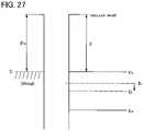
- FIG. 23is a longitudinal cross-sectional view of an inverted staggered transistor in which an oxide semiconductor is used
- FIG. 25shows an energy band diagram (a schematic diagram) along the section B-B′ illustrated in FIG. 23 in the case in which the gate voltage is 0 V;
- FIG. 26Ashows an energy band diagram (a schematic diagram) along B-B′ illustrated in FIG. 23 in the case in which a positive potential (V G >0) is applied to a gate (GE 1 ), and FIG. 26B shows an energy band diagram (a schematic diagram) along B-B′ illustrated in FIG. 23 in the case in which a negative potential (V G ⁇ 0) is applied to the gate (GE 1 ); and
- FIG. 27shows a relation between the vacuum level and the work function of a metal ( ⁇ M), and between the vacuum level and the electron affinity of an oxide semiconductor ( ⁇ ).
- FIGS. 1A to 1Eone embodiment of a substrate provided with a circuit of a display device and a manufacturing method of the substrate provided with a circuit as one embodiment of a semiconductor device and a manufacturing method of the semiconductor device will be described with reference to FIGS. 1A to 1E .
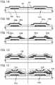
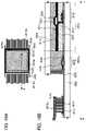
- FIG. 1Eillustrates an example of a cross-sectional structure of a plurality of transistors formed over a substrate provided with a circuit of a display device.
- Transistors 440 A and 440 B illustrated in FIG. 1Eeach have a kind of four-terminal structure in which a pair of electrode layers which are provided on opposite sides from each other with respect to a channel formation region of an oxide semiconductor layer, each with an insulating film arranged therebetween.
- a so-called dual-gate transistor in which a pair of electrode layers which are provided on opposite sides from each other with respect to a channel formation region of an oxide semiconductor layer, each with an insulating film arranged therebetweenis one embodiment of the four-terminal structure of this embodiment.
- the transistor 440 Bis applied to a pixel of a display device and the transistor 440 A is applied to part of a driver circuit arranged in the periphery of a pixel portion will be described.
- the transistor 440 Aincludes a first electrode layer 421 a , a first insulating layer 402 , an oxide semiconductor layer 404 a including a crystalline region 405 a , a second electrode layer 455 a , and a third electrode layer 455 b over a substrate 400 having an insulating surface.
- the transistor 440 Aincludes a second insulating layer 428 which is in contact with the crystalline region 405 a and covers the transistor 440 A, and a fourth electrode layer 422 a which is provided over a channel formation region with the second insulating layer 428 interposed therebetween.
- the first electrode layer 421 a and the oxide semiconductor layer 404 a including the crystalline region 405 aoverlap with each other with the first insulating layer 402 interposed therebetween. Further, the second electrode layer 455 a and the third electrode layer 455 b are formed over the oxide semiconductor layer 404 a so that part of the second electrode layer 455 a part of the third electrode layer 455 b overlap with the oxide semiconductor layer 404 a.
- the transistor 440 Bincludes a first electrode layer 421 b , the first insulating layer 402 , an oxide semiconductor layer 404 b including a crystalline region 405 b , a second electrode layer 455 c , and a third electrode layer 455 d over the substrate 400 having an insulating surface.
- the transistor 440 Bincludes the second insulating layer 428 which is in contact with the crystalline region 405 b and covers the transistor 440 B and a fourth electrode layer 422 b which is provided over the channel formation region with the second insulating layer 428 interposed therebetween.
- the first electrode layer 421 b and the oxide semiconductor layer 404 b including the crystalline region 405 boverlap with each other with the first insulating layer 402 interposed therebetween.
- the second electrode layer 455 c and the third electrode layer 455 dare formed over the oxide semiconductor layer 404 b so that part of the second electrode layer 455 c part of the third electrode layer 455 d overlap with the oxide semiconductor layer 404
- the transistors 440 A and 440 Beach have a dual-gate structure.
- a transistor having a dual-gate structureone or both of electrode layers which are provided on opposite sides from each other with respect to an oxide semiconductor layer, each with an insulating film arranged therebetween can be used as a gate electrode layer.
- the second electrode layer and the third electrode layerfunction as a source electrode layer and a drain electrode layer.
- the fourth electrode layer 422 a of the transistor 440 Ais used as a main gate electrode of the transistor. Accordingly, a channel is formed in a region which is positioned between a region in contact with the second electrode layer 455 a of the oxide semiconductor layer 404 a and a region in contact with the third electrode layer 455 b of the oxide semiconductor layer 404 a , which is in contact with the second insulating layer 428 , and which overlaps with the fourth electrode layer 422 a.
- the first electrode layer and the fourth electrode layerare provided on opposite sides from each other with respect to the oxide semiconductor layer, each with the insulating film arranged therebetween.
- the first electrode layerin the case where the potential of the first electrode layer is higher that that of the fourth electrode layer, the first electrode layer is referred to as a main gate electrode, and in the case where the potential of the fourth electrode layer is higher that that of the first electrode layer, the fourth electrode layer is referred to as a main gate electrode.
- the potential of either the first electrode layer or the fourth electrode layermay be GND, 0 V, or in a floating state.
- the first electrode layer 421 b of the transistor 440 Bis used as a main gate electrode of the transistor. Accordingly, a channel is formed in a region which is positioned between a region in contact with the second electrode layer 455 c of the oxide semiconductor layer 404 b and a region in contact with the third electrode layer 455 d of the oxide semiconductor layer 404 b , which is in contact with the first insulating layer 402 , and which overlaps with the first electrode layer 421 b.
- the transistor 440 Bcan have a light-transmitting property when the first electrode layer 421 b , the second electrode layer 455 c , the third electrode layer 455 b , and the fourth electrode layer 422 b are formed using a light-transmitting conductive film.
- the aperture ratio of the pixelcan be improved.
- depositionmay be performed with a target including SiO 2 at greater than or equal to 2 wt % and less than or equal to 10 wt % so that the light-transmitting conductive film may include SiO x (X>0) and be amorphous.
- the first electrode layer 421 a , the second electrode layer 455 a , the third electrode layer 455 b , and the fourth electrode layer 422 a of the transistor 440 Amay be formed using a single-layer structure or a stacked structure including a film containing an element selected from Ti, Mo, W, Al, Cr, Cu, and Ta as a main component.
- a material including metal with high oxygen affinityis preferably used for the second electrode layer 455 a and the third electrode layer 455 b which are electrically connected to the oxide semiconductor layer.
- an In—Sn—Ga—Zn—O-based oxide semiconductor layerwhich is a four-component metal oxide; an In—Ga—Zn—O-based oxide semiconductor layer, an In—Sn—Zn—O-based oxide semiconductor layer, an In—Al—Zn—O-based oxide semiconductor layer, a Sn—Ga—Zn—O-based oxide semiconductor layer, an Al—Ga—Zn—O-based oxide semiconductor layer, or a Sn—Al—Zn—O-based oxide semiconductor layer which are three-component metal oxides; an In—Zn—O-based oxide semiconductor layer, a Sn—Zn—O-based oxide semiconductor layer, an Al—Zn—O-based oxide semiconductor layer, a Zn—Mg—O-based oxide semiconductor layer, a Sn—Mg—O-based oxide semiconductor layer, or an In—Mg—O-based oxide semiconductor layer which are two-component metal oxides; or an In—O-based oxide semiconductor layer, a Sn—Sn—Ga
- a thin film represented by InMO 3 (ZnO) m (m>0)can be used as the oxide semiconductor layer.
- Mrepresents one or more metal elements selected from Ga, Al, Mn, and Co.
- Mmay be Ga, Ga and Al, Ga and Mn, Ga and Co, or the like.
- An oxide semiconductor layer whose composition formula is represented by InMO 3 (ZnO) m (m>0), which includes Ga as M,is referred to as an In—Ga—Zn—O-based oxide semiconductor described above, and a thin film of the In—Ga—Zn—O oxide semiconductor is also referred to as an In—Ga—Zn—O-based film.
- the oxide semiconductor layerFor the oxide semiconductor layer, the one which is subjected to dehydration or dehydrogenation at high temperature in a short time by a rapid thermal annealing (RTA) method or the like is used.
- RTArapid thermal annealing
- This heating processmakes a superficial portion of the oxide semiconductor layer have a crystalline region including so-called nanocrystals with a grain size of greater than or equal to 1 nm and less than or equal to 20 nm and the rest of the oxide semiconductor layer is amorphous or is formed of a mixture of amorphousness and microcrystals, where an amorphous region is dotted with microcrystals.
- the above-described size of the nanocrystalis just an example, and the present invention is not construed as being limited to the above range.
- an oxide semiconductor layer having such a structurea dense crystalline region including nanocrystals exists in its superficial portion. Therefore, in the case of using such an oxide semiconductor layer, a change to an n-type, which is attributed to entry of moisture to the superficial portion or elimination of oxygen from the superficial portion, can be prevented. As a result, deterioration of electric characteristics influenced by a change to an n-type, specifically increase in the off-state current can be prevented.
- the crystalline region in the superficial portion of the oxide semiconductor layerincludes crystal grains in which c-axes are oriented in a direction substantially perpendicular to a surface of the oxide semiconductor layer.
- the c-axes of the crystal grains of In 2 Ga 2 ZnO 7 in the crystalline regionare oriented in a direction substantially perpendicular to the surface of the oxide semiconductor layer.
- the crystalline regionincludes nanocrystals which are oriented in a predetermined direction.
- an In—Ga—Zn—O-based oxide semiconductor materialis used for the oxide semiconductor layer and nanocrystals are arranged so that c-axes of In 2 Ga 2 ZnO 7 are oriented in a direction substantially perpendicular to a substrate plane (or the surface of the oxide semiconductor layer), current flows in a b-axis direction (or an a-axis direction) of In 2 Ga 2 ZnO 7 in the transistor.
- the crystalline regionmay include a portion other than the crystal grains.
- the crystal structure of the crystal grainsis not limited to the above structure, and the crystalline region may include crystal grains of another structure.
- crystal grains of InGaZnO 4may be included in addition to the crystal grains of In 2 Ga 2 ZnO 7 .
- a conductive filmis formed over the substrate 400 having an insulating surface and a first photolithography step is performed thereon to form the first electrode layer 421 a and the first electrode layer 421 b .
- etchingis preferably performed so that at least an end portion of the first electrode layer 421 a and the first electrode layer 421 b be tapered in order to prevent disconnection.
- a resist maskmay be formed by an inkjet method. Formation of the resist mask by an inkjet method needs no photomask; thus, manufacturing cost can be reduced. Needless to say, an inkjet method can be applied not only to the first photolithography step but also to another photolithography step.
- any of the following substratescan be used: non-alkaline glass substrates formed using barium borosilicate glass, aluminoborosilicate glass, aluminosilicate glass, and the like by a fusion method or a float method; ceramic substrates; plastic substrates having heat resistance enough to withstand a process temperature of this manufacturing process; and the like.
- a metal substratesuch as a stainless steel alloy substrate which is provided with an insulating film over the surface may also be used.
- a substrate formed of an insulator such as a ceramic substrate, a quartz substrate, or a sapphire substratemay be used.
- a crystallized glass substrate or the likemay be used.
- the first electrode layer 421 a and the first electrode layer 421 bcan be formed using a single layer or a stacked layer using any of the following: a metal material such as aluminum, copper, molybdenum, titanium, chromium, tantalum, tungsten, neodymium, or scandium; an alloy material which contains any of these materials as a main component; and a nitride containing any of these materials.
- a metal materialsuch as aluminum, copper, molybdenum, titanium, chromium, tantalum, tungsten, neodymium, or scandium
- an alloy material which contains any of these materials as a main componentand a nitride containing any of these materials.
- the low-resistance metal materialis preferably used in combination with a refractory metal material because it has disadvantages such as low heat resistance and a tendency to be corroded.
- the refractory metal materialmolybdenum, titanium, chromium, tanta
- a light-transmitting oxide conductive layeris used for part of the electrode layer and the wiring layer to increase the aperture ratio.
- an oxide conductive layer including indium oxide, an alloy of indium oxide and tin oxide, an alloy of indium oxide and zinc oxide, zinc oxide, zinc aluminum oxide, zinc aluminum oxynitride, zinc gallium oxide, or the likecan be used for the light-transmitting conductive layer.
- the first electrode layer 421 a and the first electrode layer 421 bmay be formed using different materials.
- the first electrode layer 421 bcan be formed using a light-transmitting conductive layer with respect to visible light, and in order to suppress wiring resistance, the first electrode layer 421 a in a driver circuit portion can be formed using a conductive film including metal as its main component, for example, a single film containing an element selected from titanium, molybdenum, tungsten, aluminum, chromium, copper, and tantalum as a main component or a stacked layer film including the film.
- An insulating layer serving as a base filmmay be provided between the substrate 400 and the first electrode layers 421 a and 421 b .
- the base filmhas a function of preventing diffusion of an impurity element from the substrate 400 , and can be formed to have a single-layer or stacked-layer structure including one or more of a silicon nitride film, a silicon oxide film, a silicon nitride oxide film, and a silicon oxynitride film.
- the first insulating layer 402is formed over the first electrode layer 421 a and the first electrode layer 421 b .
- a single-layer film or a stacked-layer film of any of silicon oxide layer, silicon oxynitride layer, silicon nitride oxide layer, silicon nitride layer, aluminum oxide layer, tantalum oxide layer, and the likecan be used.
- the first insulating layer 402is formed to a thickness greater than or equal to 50 nm and less than or equal to 250 nm with a CVD method, a sputtering method, or the like. Note that in the first insulating layer 402 , an oxide insulating layer is provided preferably on the side where the first insulating layer 402 is in contact with the oxide semiconductor layer.
- the oxide semiconductor which becomes i-type or becomes substantially i-type (an oxide semiconductor which is purified) due to removal of an impurityis extremely sensitive to an interface state density or an interface electric charge; therefore, an interface with the insulating film is important. Accordingly, the insulating film which is in contact with the oxide semiconductor with high purity needs to be of high quality.
- high-density plasma CVD using microwaves (2.45 GHz)is preferable in that it produces a dense high-quality insulating film with high dielectric withstand voltage. This is because a close contact between an oxide semiconductor with high purity and a high-quality gate insulating film reduces interface state density and produces favorable interface characteristics.
- the insulating film formed using the high-density plasma CVD apparatuscan have a uniform thickness, the insulating film has excellent step coverage. Further, the thickness of a thin insulating film formed with the high-density plasma CVD apparatus can be controlled precisely.
- sputtering method or plasma CVD methodcan be employed as long as the method enables formation of a good-quality insulating film as a gate insulating film.
- an insulating film whose film quality and interface characteristics with the oxide semiconductor are improved by heat treatment performed after formation of the insulating filmmay be used.
- any insulating film that has a reduced interface state density with the oxide semiconductor and can form a favorable interface as well as having a favorable film quality as a gate insulating filmcan be used.
- the first insulating layer 402is formed using a high-density plasma CVD apparatus.
- a high-density plasma CVD apparatusrefers to an apparatus which can realize a plasma density higher than or equal to 1 ⁇ 10 11 /cm 3 .
- plasmais generated by applying a microwave power higher than or equal to 3 kW and lower than or equal to 6 kW so that the insulating film is formed.
- a monosilane gas (SiH 4 ), nitrous oxide (N 2 O), and a rare gasare introduced into a chamber as a source gas to generate high-density plasma at a pressure higher than or equal to 10 Pa and lower than or equal to 30 Pa so that an insulating film is formed over a substrate having an insulating surface, such as a glass substrate.
- the supply of a monosilane gasmay be stopped, and nitrous oxide (N 2 O) and a rare gas may be introduced without exposure to the air to perform plasma treatment performed on a surface of the insulating film.
- the plasma treatment performed on the surface of the insulating film by introducing nitrous oxide (N 2 O) and a rare gasis performed at least after the insulating film is formed.
- the insulating film formed through the above process procedurehas a small thickness and is an insulating film whose reliability can be ensured even though it has a thickness less than 100 nm, for example.
- the flow ratio of a monosilane gas (SiH 4 ) to nitrous oxide (N 2 O) which are introduced into the chamberis in the range of 1:10 to 1:200.
- a rare gas which is introduced into the chamberhelium, argon, krypton, xenon, or the like can be used.
- argonwhich is inexpensive, is preferably used.
- the insulating film formed by using the high-density plasma apparatuscan have a uniform thickness, the insulating film has excellent step coverage. Further, with the high-density plasma apparatus, the thickness of a thin insulating film can be controlled precisely.
- the insulating film formed through the above process procedureis greatly different from the insulating film formed using a conventional parallel plate PCVD apparatus.
- the etching rate of the insulating film formed through the above process procedureis lower than that of the insulating film formed using the conventional parallel plate PCVD apparatus by greater than or equal to 10% or greater than or equal to 20% in the case where the etching rates with the same etchant are compared to each other.
- the insulating film formed using the high-density plasma apparatusis a dense film.
- a silicon oxide layer formed by a CVD method using an organosilane gascan be used for the first insulating layer 402 .
- an organosilane gasa silicon-containing compound such as tetraethoxysilane (TEOS) (chemical formula: Si(OC 2 H 5 ) 4 ), tetramethylsilane (TMS) (chemical formula: Si(CH 3 ) 4 ), tetramethylcyclotetrasiloxane (TMCTS), octamethylcyclotetrasiloxane (OMCTS), hexamethyldisilazane (HMDS), triethoxysilane (chemical formula: SiH(OC 2 H 5 ) 3 ), or trisdimethylaminosilane (chemical formula: SiH(N(CH 3 ) 2 ) 3 ) can be used.
- TEOStetraethoxysilane
- TMStetramethylsilane
- TMStetramethylsilane
- the first insulating layer 402may be formed using one kind of oxide, nitride, oxynitride, and nitride oxide of aluminum, yttrium, or hafnium; or a compound including at least two or more kinds of the above.
- oxynitriderefers to a substance that contains more oxygen atoms than nitrogen atoms and nitride oxide refers to a substance that contains more nitrogen atoms than oxygen atoms.
- a “silicon oxynitride film”means a film that contains oxygen atoms and nitrogen atoms so that the number of the oxygen atoms is larger than that of the nitrogen atoms and, in the case where measurements are performed using Rutherford backscattering spectrometry (RBS) and hydrogen forward scattering (HFS), contains oxygen, nitrogen, silicon, and hydrogen at concentrations ranging from 50 atomic % to 70 atomic %, 0.5 atomic % to 15 atomic %, 25 atomic % to 35 atomic %, and 0.1 atomic % to 10 atomic %, respectively.
- RBSRutherford backscattering spectrometry
- HFShydrogen forward scattering
- a “silicon nitride oxide film”means a film that contains nitrogen atoms and oxygen atoms so that the number of the nitrogen atoms is larger than that of the oxygen atoms and, in the case where measurements are performed using RBS and HFS, contains oxygen, nitrogen, silicon, and hydrogen at concentrations ranging from 5 atomic % to 30 atomic %, 20 atomic % to 55 atomic %, 25 atomic % to 35 atomic %, and 10 atomic % to 30 atomic %, respectively. Note that percentages of nitrogen, oxygen, silicon, and hydrogen fall within the ranges given above when the total number of atoms contained in the silicon oxynitride film or the silicon nitride oxide film is defined as 100 atomic %.
- an oxide semiconductor film 403is formed to a thickness greater than or equal to 5 nm and less than or equal to 200 nm, preferably greater than or equal to 10 nm and less than or equal to 20 nm (see FIG. 1A ).
- dust on a surface of the first insulating layer 402is preferably removed by reverse sputtering in which an argon gas is introduced and plasma is generated.
- the reverse sputteringrefers to a method in which, without application of voltage to a target side, an RF power source is used for application of voltage to a substrate side in an argon atmosphere to generate plasma in the vicinity of the substrate to modify a surface.
- an argon atmosphereinstead of an argon atmosphere, a nitrogen atmosphere, a helium atmosphere, or the like may be used. Alternatively, an argon atmosphere to which oxygen, N 2 O, or the like is added may be used.
- an argon atmosphere to which Cl 2 , CF 4 , or the like is addedmay be used. After the reverse sputtering, the oxide semiconductor film is formed without being exposed to air, whereby dust or moisture can be prevented from attaching to an interface between the first insulating layer 402 and the oxide semiconductor film 403 .
- an In—Sn—Ga—Zn—O-based oxide semiconductor layerwhich is a four-component metal oxide described above; an In—Ga—Zn—O-based oxide semiconductor layer, an In—Sn—Zn—O-based oxide semiconductor layer, an In—Al—Zn—O-based oxide semiconductor layer, a Sn—Ga—Zn—O-based oxide semiconductor layer, an Al—Ga—Zn—O-based oxide semiconductor layer, or a Sn—Al—Zn—O-based oxide semiconductor layer which are three-component metal oxides described above; an In—Zn—O-based oxide semiconductor layer, a Sn—Zn—O-based oxide semiconductor layer, an Al—Zn—O-based oxide semiconductor layer, a Zn—Mg—O-based oxide semiconductor layer, a Sn—Mg—O-based oxide semiconductor layer, or an In—Mg—O-based oxide semiconductor layer which are two-component metal oxides described above; or an In—O-based oxide semiconductor layer
- the oxide semiconductor filmcan be formed with a sputtering method in a rare gas (typically argon) atmosphere, an oxygen atmosphere, or an atmosphere of a rare gas (typically argon) and oxygen.
- a sputtering methodfilm deposition may be performed using a target containing SiO 2 at greater than or equal to 2 percent by weight and less than or equal to 10 percent by weight and SiOx (x>0) which inhibits crystallization may be contained in the oxide semiconductor film.
- a pulse direct current (DC) power sourceis preferable because powder substances (also referred to as particles or dust) generated in film formation can be reduced and the film thickness distribution can be uniform.
- an In—Ga—Zn—O-based film having a thickness of 15 nmis formed with a sputtering method using a target for forming an In—Ga—Zn—O-based oxide semiconductor.
- the oxide semiconductor filmis preferably formed while moisture remaining in the treatment chamber is removed. This is for preventing hydrogen, a hydroxyl group, or moisture from being contained in the oxide semiconductor film.
- the oxide semiconductor filmbe successively formed over the first insulating layer 402 .
- the multi-chamber sputtering apparatus used hereis provided with the target of silicon or silicon oxide (artificial quarts), and the target for formation of an oxide semiconductor film.
- the deposition chamber provided with the target for formation of an oxide semiconductor filmis also provided with at least a cryopump as an evacuation unit. Note that a turbo molecular pump may be used instead of the cryopump, and a cold trap may be provided above an inlet of the turbo molecular pump so that moisture or the like may be adsorbed.
- a hydrogen atom, a compound containing a hydrogen atom such as H 2 O, a carbon atom, a compound containing a carbon atom, and the likeare removed, whereby the concentration of an impurity in the oxide semiconductor film formed in the deposition chamber can be reduced.
- a high-purity gas in which an impurity such as hydrogen, water, a hydroxyl group, or hydride is reduced to approximately the ppm level or the ppb levelbe used as the sputtering gas for the deposition of the oxide semiconductor film.
- the oxide semiconductor filmmay be formed in the state where the substrate is heated. At that time, the substrate is heated higher than or equal to 100° C. and lower than or equal to 600° C., preferably, higher than or equal to 200° C. and lower than or equal to 400° C. By heating the substrate during deposition, the impurity concentration in the oxide semiconductor film can be reduced.
- Examples of a sputtering methodinclude an RF sputtering method in which a high-frequency power source is used as a sputtering power source, a DC sputtering method in which a direct-current power source is used, and a pulsed DC sputtering method in which a bias is applied in a pulsed manner.
- An RF sputtering methodis mainly used in the case of forming an insulating film
- a DC sputtering methodis mainly used in the case of forming a metal conductive film.
- multi-source sputtering apparatusin which a plurality of targets of different materials can be set.
- films of different materialscan be formed to be stacked in the same chamber, or a film of plural kinds of materials can be formed by electric discharge at the same time in the same chamber.
- a sputtering apparatusprovided with a magnet system inside the chamber and used for magnetron sputtering, and a sputtering apparatus used for ECR sputtering in which plasma generated with the use of microwaves is used without using glow discharge.
- a deposition method by sputteringthere are also a reactive sputtering method in which a target substance and a sputtering gas component are chemically reacted with each other during deposition to form a thin compound film thereof, and a bias sputtering method in which a voltage is also applied to a substrate during deposition.
- a resist maskis formed.
- the In—Ga—Zn—O-based filmis etched.
- organic acidsuch as citric acid or oxalic acid can be used for etchant.
- Etchingis performed so that the end portions of the oxide semiconductor layers 404 a and 404 b have tapered shapes, breakage of a wiring due to a step shape can be prevented. Note that etching here is not limited to wet etching and dry etching may also be used.
- First heat treatment for the dehydration or dehydrogenationcan be performed with the use of resistance heating method, lamp irradiation, or the like in an inert gas atmosphere through rapid thermal annealing (RTA) treatment at a temperature higher than or equal to 500° C. and lower than or equal to 750° C. (or a temperature lower than or equal to the strain point of a glass substrate) for approximately one minute to ten minutes, preferably at 650° C. for approximately greater than or equal to three minutes and less than or equal to six minutes.
- RTArapid thermal annealing
- dehydration or dehydrogenationcan be performed in a short time; therefore, treatment can be performed even at a temperature higher than the strain point of a glass substrate.
- the timing of heat treatmentis not limited to this timing and may be performed plural times, for example, before and after a photolithography step or a deposition step.
- heat treatment in the atmosphere of an inert gas such as nitrogen or a rare gasis referred to as heat treatment for dehydration or dehydrogenation.
- dehydrogenationdoes not refer to only elimination in the form of H 2 by the heat treatment, and dehydration or dehydrogenation also refers to elimination of H, OH, and the like for convenience.
- the temperatureis decreased from the heating temperature T at which the oxide semiconductor layer is dehydrated or dehydrogenated to room temperature in the same furnace used for the dehydration or dehydrogenation with the oxide semiconductor layer prevented from being exposed to air so that entry of water or hydrogen into the oxide semiconductor layer is prevented.
- the threshold voltage of the transistorcan be positive, so that a switching element having so-called normally-off characteristics can be realized. It is preferable that a channel in a transistor of a display device be formed at a positive threshold voltage which is as close to 0 V as possible.
- the threshold voltage of the transistoris negative, it tends to be normally on; in other words, current flows between the source electrode and the drain electrode even when the gate voltage is 0 V.
- the threshold voltageV th
- the threshold voltage valueis high or is on the minus side even when the field effect mobility is high, it is difficult to control the circuit.
- the transistorcannot perform a switching function as a transistor and might be a load when a transistor is driven at low voltage.
- n-channel transistorIn the case of an n-channel transistor, it is desirable that only after a positive voltage is applied as a gate voltage, a channel be formed and a drain current flows.
- a transistor in which a channel is not formed unless driving voltage is raised and a transistor in which a channel is formed and drain current flows even when negative voltage is appliedare unsuitable for a transistor used in a circuit.
- the gas atmospheremay be switched to a gas atmosphere which is different from that used when the temperature is raised to the heating temperature T.
- coolingis performed by using the same furnace that is used for the dehydration or dehydrogenation and by filling the furnace with a high-purity oxygen gas, a high-purity N 2 O gas, or ultra-dry air (having a dew point of ⁇ 40° C. or lower, preferably ⁇ 60° C. or lower) without exposure to the air.
- the purity of an inert gas which is introduced into a heat treatment apparatusis preferably 6N (99.9999%) or more, more preferably 7N (99.99999%) or more (that is, the impurity concentration is 1 ppm or less, preferably 0.1 ppm or less).
- an oxide semiconductor layeris changed into an oxygen-deficient oxide semiconductor layer by the heat treatment to be a low-resistant oxide semiconductor layer, i.e. an n-type (e.g., n ⁇ -type) oxide semiconductor layer.
- oxygenis supplied to an oxygen-deficient portion of the oxide semiconductor layer by the formation of an oxide insulating layer which is in contact with the oxide semiconductor layer.
- the oxide semiconductor layeris made to be i-type; that is, the oxide semiconductor layer is changed into a high-resistance oxide semiconductor layer. Accordingly, it is possible to form a highly reliable transistor having favorable electric characteristics.
- the oxide semiconductor layerwhich is sufficiently dehydrated or dehydrogenated under the above conditions, at least a peak at around higher than or equal to 250° C. and lower than or equal to 300° C. of two peaks in spectra which show discharge of moisture is not detected with thermal desorption spectroscopy (TDS) even when the temperature of the dehydrated or dehydrogenated oxide semiconductor layer is increased to 450° C.
- TDSthermal desorption spectroscopy
- the oxide semiconductor layer 404 a and the oxide semiconductor layer 404 bare each an amorphous layer having many dangling bonds at the stage where the oxide semiconductor layers 404 a and 404 b are in an as-depo state.
- a first heating step for the dehydration or dehydrogenationdangling bonds that exist close to each other are bonded, so that the oxide semiconductor layers 404 a and 404 b can have an ordered amorphous structure.
- the oxide semiconductor layers 404 a and 404 bare formed of a mixture of amorphousness and microcrystals, where an amorphous region is dotted with microcrystals, or are formed of amorphousness.
- the crystalline region 405 a and the crystalline region 405 b including nanocrystalsare formed in the superficial portion of the oxide semiconductor layer 404 a and the oxide semiconductor layer 404 b ( FIG. 1B ).
- the rest of the oxide semiconductor layer 404 a and the oxide semiconductor layer 404 bcome to be amorphous or be formed of a mixture of amorphousness and microcrystals, where an amorphous region is dotted with microcrystals.
- the crystalline region 405 a and the crystalline region 405 bare part of the oxide semiconductor layer 404 a and the oxide semiconductor layer 404 b respectively, and hereinafter, the “the oxide semiconductor layer 404 a ” and “the oxide semiconductor layer 404 b ” includes the crystalline region 405 a and the crystalline region 405 b , respectively.
- the microcrystalis a so-called nanocrystal with a particle size greater than or equal to 1 nm and less than or equal to 20 nm, which is smaller than that of a microcrystalline particle generally called a microcrystal.
- a nanocrystal which is c-axis-oriented in a direction perpendicular to a surface of the layeris preferably formed.
- the long axis of the crystalis in the c-axis direction and the size in the short-axis direction is greater or equal to 1 nm and less or equal to 20 nm.
- the crystalline regionis not formed in a side surface portion of the oxide semiconductor layer depending on the order of steps, and in such a case, the crystalline region is formed only in a superficial portion, except for the side surface portion.
- the area of the side surface portionis small, and the effect of suppressing the deterioration of electric characteristics or improving the dielectric withstand voltage can be maintained in that case as well.
- the first electrode layer 421 a and the first electrode layer 421 bare crystallized to be microcrystalline layers or polycrystalline layers in some cases, depending on the condition of the first heat treatment or a material of the first electrode layers 421 a and 421 b .
- the first heat treatmentat 450° C. for one hour
- an indium tin oxide containing a silicon oxideis used as the first electrode layers 421 a and 421 b , they are not easily crystallized.
- the oxide semiconductor layers 404 a and 404 b after the first heat treatmentare oxygen-deficient oxide semiconductor layers, and the carrier concentration is higher than the carrier concentration right after the deposition and preferably 1 ⁇ 10 18 /cm 3 or more. Thus the oxide semiconductor layers 404 a and 404 b have lower resistance.
- the first heat treatment for the oxide semiconductor layerscan be performed before the oxide semiconductor film is processed into the island-shaped oxide semiconductor layers.
- the substrateis taken out of the heating apparatus and subjected to a photolithography step to form the island-shaped oxide semiconductor layers.
- an opening(also referred to as a contact hole) for connecting the first electrode layer to the source electrode layer or the drain electrode layer which will be described later is formed in the first insulating layer 402 .
- the contact holeis formed by forming a mask over the first insulating layer 402 by a photolithography method, an inkjet method, or the like, and then selectively etching the first insulating layer 402 using the mask. Note that the contact hole may be formed after the formation of the first insulating layer 402 and before the formation of the oxide semiconductor film 403 .
- a conductive film which to be as a source electrode and a drain electrode(including wires formed in the same layer as the source electrode and the drain electrode) is formed over the oxide semiconductor layers 404 a and 404 b .
- the conductive filmis formed with a thickness greater than or equal to 100 and less than or equal to 500 nm, preferably greater than or equal to 200 and less than or equal to 300 nm.
- the source electrode and the drain electrodeare formed using a metal material such as Al, Cu, Cr, Ta, Ti, Mo, or W, or an alloy material containing any of these metal materials as its component.
- a structuremay be employed in which a high-melting-point metal layer of Cr, Ta, Ti, Mo, W, or the like is stacked over one side or both sides of a metal layer of Al, Cu, or the like.
- Heat resistancecan be increased by using an Al material into which an element such as Si, Ti, Ta, W, Mo, Cr, Nd, Sc or Y which prevents the generation of hillocks or whiskers on the Al film is added.
- the source electrode and the drain electrodemay be formed using a conductive metal oxide.
- a conductive metal oxideindium oxide (In 2 O 3 ), tin oxide (SnO 2 ), zinc oxide (ZnO), an indium oxide-tin oxide alloy (In 2 O 3 —SnO 2 , abbreviated to ITO), indium oxide and zinc oxide (In 2 O 3 —ZnO), or a material which is added silicon or silicon oxide to the metal oxide material can be used.
- the metal conductive filmis not limited to a single layer containing the above-described element and may be two or more layers. However, a material of the conductive film preferably has heat resistance that can withstand at least second heat treatment performed later.
- a material including metal with high oxygen affinityis preferable.
- the metal with high oxygen affinityone or more materials selected from titanium (Ti), manganese (Mn), magnesium (Mg), zirconium (Zr), beryllium (Be), and thorium (Th) are preferable.
- a titanium filmis used.
- the oxide semiconductor layer and the conductive film with high oxygen affinityWhen the oxide semiconductor layer and the conductive film with high oxygen affinity are formed in contact with each other, the carrier density in the vicinity of the interface is increased and a low-resistance region is formed, whereby the contact resistance between the oxide semiconductor layer and the conductive film can be reduced.
- the conductive film with high oxygen affinityextracts oxygen from the oxide semiconductor layer and thus either or both a layer which includes metal in the oxide semiconductor layer in excess (such a layer is referred to as a composite layer) and an oxidized conductive film are formed in the interface between the oxide semiconductor layer and the conductive film.
- an indium-excess layer and a titanium oxide layerare formed in the vicinity of the interface where the oxide semiconductor layer is in contact with the titanium film in some cases. In other cases, either one of the indium-excess layer and the titanium oxide layer is formed in the vicinity of the interface where the oxide semiconductor layer is in contact with the titanium film.
- the indium-excess layer which is an oxygen-deficient In—Ga—Zn—O-based oxide semiconductor layerhas high electric conductivity; therefore, the contact resistance between the oxide semiconductor layer and the conductive film can be reduced.
- a titanium film or a titanium oxide film having conductivitymay be used as the conductive film which is in contact with the oxide semiconductor layer.
- an indium-excess layermight be formed in the vicinity of the interface where the oxide semiconductor layer is in contact with the titanium oxide film.
- a conductive material having a light-transmitting property with respect to visible lightcan be used.
- a transparent conductive oxide including any of indium, tin, or zincis preferable.
- indium oxide (In 2 O 3 ) or an indium oxide-tin oxide alloy (In 2 O 3 —SnO 2 , abbreviated to ITO)can be used.
- a transparent conductive oxide to which an insulating oxide such as silicon oxide is addedmay be used.
- the conductive filmAs a formation method of the conductive film, an arc discharge ion plating method or a spray method may be employed.
- the conductive filmmay be formed by discharging a conductive nanopaste of silver, gold, copper, or the like by a screen printing method, an ink-jet method, or the like and baking the nanopaste.
- a maskis formed over the conductive film by a photolithography method, an inkjet method, or the like and the conductive film is etched using the mask; thus, the source electrode and the drain electrode are formed ( FIG. 1C ).
- a 200-nm-thick Ti filmis formed by a sputtering method as the conductive film, and the conductive film is selectively etched by a wet etching method or a dry etching method using a resist mask, whereby the second electrode layer 455 a , the third electrode layer 455 b , the second electrode layer 455 c , and the third electrode layer 455 d which function as the source electrodes and the drain electrodes are formed.
- the second insulating layer 428which covers the second electrode layer 455 a , the third electrode layer 455 b , the second electrode layer 455 c , the third electrode layer 455 d , and the exposed parts of the oxide semiconductor layers 404 a and 404 b is formed ( FIG. 1D ).
- the thickness of the second insulating layer 428is preferably greater than or equal to 50 nm and less than or equal to 250 nm.
- the second insulating layer 428includes an oxide insulating layer on the side where the second insulating layer 428 is in contact with the oxide semiconductor layer.
- an oxide insulating layersuch as a silicon oxide layer, a silicon oxynitride layer, an aluminum oxide layer, a tantalum oxide layer, a yttrium oxide layer, or a hafnium oxide layer is can be used.
- the oxide insulating layercan be formed as appropriate with a sputtering method or the like, i.e. a method with which impurities such as moisture or hydrogen are not mixed into the oxide insulating layer.
- a silicon oxide filmis formed as the oxide insulating layer by a sputtering method.
- the substrate temperature in the depositionmay be higher than or equal to room temperature and lower than or equal to 300° C. and in this embodiment, the substrate temperature in film formation is 100° C.
- pre-baking under reduced pressureat a temperature higher than or equal to 150° C. and lower than or equal to 350° C.
- the silicon oxide filmcan be formed by a sputtering method under a rare gas (typically, argon) atmosphere, an oxygen atmosphere, or a mixed atmosphere of a rare gas (typically, argon) and oxygen.
- a silicon oxide target or a silicon targetmay be used as a target.
- a silicon oxide filmcan be formed by a sputtering method in an atmosphere of oxygen and a rare gas.
- a structure in which an inorganic insulating film is stacked over the oxide insulating layer so as to block entry of impurities such as moisture, a hydrogen ion, OH ⁇ to the oxide semiconductor layer from the outsideis preferable.
- the inorganic insulating film stacked over the oxide insulating layer of the second insulating layer 428a silicon oxide layer, a silicon oxynitride layer, a silicon nitride oxide layer, a silicon nitride layer, an aluminum oxide layer, a tantalum oxide layer, or the like can be used.
- depositionis performed by a pulsed DC sputtering method with the use of a columnar polycrystalline, boron-doped silicon target having a purity of 6N (with a resistivity of 0.01 ⁇ cm) under conditions where the distance between the substrate and the target (T-S distance) is 89 mm, the pressure is 0.4 Pa, the direct current (DC) power is 6 kW, and the atmosphere is an oxygen atmosphere (the proportion of the oxygen flow is 100%).
- the film thicknessis 300 nm.
- a high-purity gas in which an impurity such as hydrogen, water, a hydroxyl group, or hydride is reduced to approximately the ppm level or the ppb levelbe used as the sputtering gas for the deposition of the second insulating layer 428 .
- second heat treatmentis performed in an inert-gas atmosphere or a nitrogen atmosphere (preferably at a temperature higher than or equal to 200° C. and lower than or equal to 400° C., e.g., higher than or equal to 250° C. and lower than or equal to 350° C.).
- the second heat treatmentis performed in a nitrogen atmosphere at 250° C. for one hour.
- RTA treatmentmay be performed at high temperature for a short time as in the first heat treatment.
- the oxide insulating layeris heated in contact with the oxide semiconductor layer, oxygen is supplied to the oxygen-deficient portion of the oxide semiconductor layer whose resistance is reduced by the first heat treatment, and thus the oxide semiconductor layer can be changed into a high-resistance oxide semiconductor layer (an i-type oxide semiconductor layer).
- the second heat treatmentis performed after formation of the silicon oxide film; however, the timing of the heat treatment is not limited to the timing immediately after formation of the silicon oxide film as long as it is after deposition of the silicon oxide film.
- a photolithography stepis performed to form a resist mask, and the second insulating layer 428 is etched to form a contact hole which reaches the second electrode layer 455 d.
- the fourth electrode layer 422 a , the fourth electrode layer 422 b , and a connection electrode layer 422 c which is connected to a pixel electrode layer laterare formed by a photolithography step performed on the conductive film ( FIG. 1E ).
- the conductive filma single-layer structure or a stacked-layer structure including a film containing an element selected from Al, Cr, Cu, Ta, Ti, Mo, and W as a main component can be used. Note that in the case where the third electrode layer 455 d and the pixel electrode layer are directly connected, the connection electrode layer 422 c may be omitted.
- the fourth electrode layer 422 a of the transistor 440 Ais used as a main gate electrode of the transistor.
- the potential of the first electrode layer 421 amay be less than or equal to that of the fourth electrode layer 422 a , GND, or 0 V, or the first electrode layer 421 a may be in a floating state.
- the first electrode layer 421 b of the transistor 440 Bis used as a main gate electrode of the transistor.
- the potential of the fourth electrode layer 422 bmay be less than or equal to that of the first electrode layer 421 b , GND, or 0 V, or the fourth electrode layer 422 b may be in a floating state.
- Each of the transistorshas the four-terminal structure in which a pair of electrode layers which are provided on opposite sides from each other with respect to a channel formation region of an oxide semiconductor layer, each with an insulating film arranged therebetween, and thus the reliability of the transistors can be improved.
- a bias-temperature stress testhereinafter, referred to as a BT test
- the amount of change in threshold voltage of the thin film transistor between before and after the BT testcan be reduced.
- a structure in which the transistor which is used the first electrode layer is used as a main gate electrode is not provided with the fourth electrode layermay be employed.
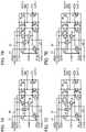
- FIG. 2an example of a cross-sectional structure of a plurality of transistors formed over a substrate with a circuit of a display device is illustrated.
- the transistor 440 A illustrated in FIG. 2has a kind of four-terminal structure in which a pair of electrode layers which are provided on opposite sides from each other with respect to a channel formation region of an oxide semiconductor layer, each with an insulating film arranged therebetween, and a transistor 450 is an inverted staggered transistor.
- the transistor 440 Ais preferably formed in a part of the driver circuit arranged in a periphery of the pixel portion of the display device, and the transistor 450 is preferably formed in part of the pixel circuit or the driver circuit or in the protective circuit.
- the transistor 450includes a first electrode layer 421 c , the first insulating layer 402 , an oxide semiconductor layer 404 c including the crystalline region 405 c , a second electrode layer 455 e , and a third electrode layer 455 f over the substrate 400 having an insulating surface.
- the transistor 450includes the second insulating layer 428 which is in contact with a crystalline region 405 c and covers the transistor 450 .
- the oxide semiconductor layer 404 coverlaps with the first electrode layer 421 c with the first insulating layer 402 provided therebetween.
- the second electrode layer 455 e and the third electrode layer 455 fare formed over the oxide semiconductor layer 404 c so that part of the second electrode layer 455 e part of the third electrode layer 455 f overlap with the oxide semiconductor layer 404 c.
- a protective insulating layermay be formed so as to cover the transistors 440 A and 450 B.
- the protective insulating layeris formed using a silicon nitride film, a silicon nitride oxide film, an aluminum nitride film, or the like.
- a planarization insulating layermay be formed over the fourth electrode layer 422 b .
- the planarization insulating layercan be formed of a heat-resistant organic material, such as an acrylic resin, polyimide, a benzocyclobutene-based resin, polyamide, or an epoxy resin. Other than such organic materials, it is also possible to use a low-dielectric constant material (a low-k material), a siloxane-based resin, PSG (phosphosilicate glass), BPSG (borophosphosilicate glass), or the like. Note that the planarization insulating layer may be formed by stacking a plurality of insulating films formed of these materials. Further, a color filter layer may be used as a planarization insulating layer.
- a storage capacitor in which the first insulating layer 402 or a dielectric layer including an oxide insulating layer is arranged between a capacitor wiring which can be formed using the same material by the same step as the first electrode layer 421 b and a capacitor electrode which can be formed using the same material by the same step as the fourth electrode layer 422 bmay be formed over the same substrate.
- the transistor 440 B and pixels including the storage capacitorare arranged in matrix so that a pixel portion is formed and the substrate in which the driver circuit including the transistor 440 A is arranged in the periphery of the pixel portion can be one substrate used to manufacture an active matrix display device.
- a power source supply linewhich is electrically connected to the source electrode layer of the transistor is provided.
- the power source supply lineintersects with a gate wiring and is formed using the same material by the same step as the connection electrode layer 422 c formed using a conductive film.
- the power source supply lineintersects with a source wiring and is formed using the same material by the same step as the first electrode layer 421 b.
- one electrode of the light-emitting elementis electrically connected to the source electrode layer or the drain electrode layer of the driving transistor, and a common potential line which is electrically connected to the other electrode of the light-emitting element is provided.
- the common potential lineis formed using the same material and through the same process as the connection electrode layer 422 c formed using a metal conductive film.
- the common potential lineis formed using the same material by the same step as the first electrode layer 421 b.
- the transistor including the oxide semiconductor layer whose concentration of hydrogen is reduced through the above-described processhas a characteristic of extremely small off-state current, which is 1 ⁇ 10 ⁇ 13 A or less.
- a transistor with small off-state currentfor example, there is a transistor using silicon carbide (e.g., 4H—SiC).
- silicon carbidee.g., 4H—SiC
- the carrier concentrationis one example of the commonalities between the oxide semiconductor and 4H—SiC.
- the minority carrier density in an oxide semiconductoris estimated to be approximately 10 ⁇ 7 /cm 3 .
- This value of the minority carrier densityis extremely small similarly to that in 4H—SiC, which is 6.7 ⁇ 10 ⁇ 11 /cm 3 .
- the minority carrier density of an oxide semiconductoris compared with the intrinsic carrier density of silicon (approximately 1.4 ⁇ 10 10 /cm 3 )
- the energy band gap of the oxide semiconductoris greater than or equal to 3.0 eV and less than or equal to 3.5 eV
- the energy band gap of 4H—SiCis 3.26 eV. Therefore, an oxide semiconductor has in common with silicon carbide in being a wide band-gap semiconductor.
- a semiconductor process using silicon carbideincludes a heat treatment for activation at higher than or equal to 1500° C. and lower than or equal to 2000° C.
- a semiconductor substrate, a semiconductor element, or the like using a semiconductor material other than silicon carbideis damaged, and thus, it is difficult to form a semiconductor element using silicon carbide over an integrated circuit using a semiconductor material other than silicon carbide.
- an oxide semiconductorcan be deposited through heat treatment at higher than or equal to 300° C. and lower than or equal to 500° C. (at a temperature lower than or equal to the glass transition temperature, approximately 700° C. at a maximum). Therefore, it is possible to form a semiconductor element using an oxide semiconductor after forming an integrated circuit using another semiconductor material.
- an oxide semiconductorIn the case of using an oxide semiconductor, there is an advantage that it is possible to use a substrate having low heat resistance such as a glass substrate, which is different from the case where silicon carbide is used. Moreover, an oxide semiconductor can be deposited without heat treatment at high temperature so that energy cost can be reduced sufficiently as compared with the case of using silicon carbide.
- DOSdensity of states
- the researchdoes not include an idea that DOS itself is reduced sufficiently.
- water and hydrogen having possibility of affecting the DOS in the energy band gapare eliminated from an oxide semiconductor, so that a purified oxide semiconductor is formed. This idea is based on the idea that the DOS itself is reduced sufficiently. Therefore, manufacture of industrial products with extremely high quality can be realized.
- oxygenmay be supplied to a metal dangling bond generated by oxygen deficiency so as to reduce the DOS due to oxygen defect, whereby more purified (i-type)oxide semiconductor can be formed.
- an oxide film having an excessive amount of oxygenmay be formed in close contact with a channel formation region, and oxygen may be supplied from the oxide film so that DOS due to the oxygen defect can be reduced.
- the defect of an oxide semiconductoris due to the level under the conduction band greater than or equal to 0.1 eV and less than or equal to 0.2 eV caused by an excessive amount of halogen, deep level caused by oxygen vacancy, or the like. Therefore, the technical idea of removing hydrogen completely and supplying oxygen sufficiently in order to eliminate those defects would be reasonable.
- an oxide semiconductoris an n-type semiconductor; however, in one embodiment of the present invention, an impurity especially water or hydrogen is removed so that an i-type oxide semiconductor is obtained.
- an impurity especially water or hydrogenis removed so that an i-type oxide semiconductor is obtained.
- one embodiment of the disclosed inventionincludes a novel technical idea because it is different from an i-type semiconductor such as silicon added with an impurity.
- a transistor using an oxide semiconductorhas some characteristics.
- the conduction mechanism of the oxide semiconductoris explained with reference to FIG. 23 , FIGS. 24A and 24B , FIG. 25 , and FIGS. 26A and 26B . Note that the following description is just a consideration and does not deny the validity of the invention.
- FIG. 23is a cross-sectional view of an inverted staggered transistor which includes an oxide semiconductor.
- An oxide semiconductor layer (OS)is provided over a gate electrode (GE 1 ) with a gate insulating film (GI) provided therebetween, and a source electrode (S) and a drain electrode (D) are provided over the oxide semiconductor layer.
- a back gate (GE 2 )is provided over the source electrode and the drain electrode with an insulating layer provided therebetween.
- FIGS. 24A and 24Bare energy band diagrams (schematic diagrams) along the section A-A′ illustrated in FIG. 23 .
- FIG. 24Billustrates a case where positive potential with respect to the source is applied to the drain (V D >0).
- FIG. 25 and FIGS. 26A and 26Bare energy band diagrams (schematic diagrams) along the section B-B′ in FIG. 23 .
- FIG. 25shows the case where the gate voltage is 0 V.
- FIG. 26Ashows a state where a positive potential (V G >0) is applied to the gate (GE 1 ), that is, a case where the transistor is in an on-state where carriers (electrons) flow between the source and the drain.
- FIG. 26Bshows a state where a negative potential (V G ⁇ 0) is applied to the gate (GE 1 ), that is, a case where the transistor is in an off state (where minority carriers do not flow).
- a depletion layerexpands to the entire oxide semiconductor in the off state. That is, the transistor can be regarded as a complete depletion transistor.
- FIG. 27shows a relation between the vacuum level and the work function of a metal ( ⁇ M ) and a relation between the vacuum level and the electron affinity of an oxide semiconductor ( ⁇ ).
- a metalis degenerated, so that the Fermi level is located in the conduction band.
- a conventional oxide semiconductoris of n-type, and the Fermi level (E f ) in that case is located closer to the conduction band and is away from the intrinsic Fermi level (E i ) that is located in the middle of the band gap.
- E fthe Fermi level
- E ithe intrinsic Fermi level
- an oxide semiconductor of the present inventionis an intrinsic (i-type) or a substantially intrinsic oxide semiconductor which is obtained in such a manner that an oxide semiconductor is purified so that an impurity other than main components of the oxide semiconductor is prevented from being contained therein as much as possible by removing hydrogen that is an n-type impurity from the oxide semiconductor.
- a featureis that a purified i-type (intrinsic) semiconductor, or a semiconductor close thereto, is obtained not by adding an impurity but by removing an impurity such as hydrogen or water as much as possible. This enables the Fermi level (E f ) to be at the same level as the intrinsic Fermi level (E i ).
- black circles ( ⁇ )represent electrons.
- the electronis injected into the oxide semiconductor over the barrier (h) and flows toward the drain.
- the height of the barrier (h)changes depending on the gate voltage and the drain voltage; in the case where a positive voltage is applied to the gate (V G >0) and a positive drain voltage is applied, the height of the barrier (h) is smaller than the height of the barrier in FIG. 24A where no voltage is applied, i.e., 1 ⁇ 2 of the band gap (E g ).
- a carrierelectron
- the height of the barrier (h)is smaller than the height of the barrier in FIG. 24A where no voltage is applied, i.e., 1 ⁇ 2 of the band gap (E g ).
- a carrierelectron
- potential barrieris reduced, and an on state where current flows is shown.
- FIG. 26Bwhen a negative potential is applied to the gate (GE 1 ), the number of holes that are minority carriers is substantially zero; thus, the current value becomes a value as close to zero as possible.
- an oxide semiconductoris made to be an intrinsic (i-type) semiconductor or made to be a substantially intrinsic semiconductor by being purified so as not to contain impurities which are not main components of the oxide semiconductor as much as possible. Therefore, interface characteristics between the gate insulating film and the oxide semiconductor become obvious, and it is necessary to consider the interface characteristics and the bulk characteristics separately. Therefore, it is necessary to use a gate insulating film which can form a favorable interface with the oxide semiconductor. For example, it is preferable to use an insulating layer which is formed by a CVD method using high-density plasma generated with a power supply frequency from the VHF band to the microwave band or an insulating film formed by a sputtering method.
- the oxide semiconductoris purified and the interface between the oxide semiconductor and the gate insulating film is favorable, even when the thin film transistor has a channel width W of 1 ⁇ 10 4 ⁇ m and a channel length of 3 ⁇ m, an off-state current of 10 ⁇ 13 A or lower at room temperature and a subthreshold value (S value) of 0.1 V/dec. (the thickness of the gate insulating film: 100 nm) are greatly expected.
- the oxide semiconductoris purified so as to minimize the amount of impurities that are not main components of the oxide semiconductor but contained in the oxide semiconductor, whereby favorable operation of the transistor can be obtained.
- a transistorin this embodiment, includes a purified oxide semiconductor layer.
- the oxide semiconductor layerincludes a dense crystalline region including nanocrystals in a surface portion of the oxide semiconductor layer, and the dense crystalline region prevents the transistor from changing into an n-type transistor due to entry of moisture from the superficial portion to the inside of the purified oxide semiconductor layer or elimination of oxygen.
- Such a transistor having a four-terminal structure in which a pair of electrode layers which are provided on opposite sides from each other with respect to the purified oxide semiconductor layer, each with an insulating film arranged therebetweenis characterized by a positive threshold voltage and an extremely small off-state current.
- a channelis formed in a region which is provided between a region in contact with the second electrode layer of the oxide semiconductor layer and a region in contact with the third electrode layer of the oxide semiconductor layer, which is in contact with the second insulating layer, and which overlaps with the fourth electrode layer.
- a region in which the channel is formedis a crystalline region of the oxide semiconductor as well, and includes the crystal grains in which c-axis is oriented in an almost vertical direction with respect to the surface of the oxide semiconductor layer.
- nanocrystalsare arranged so that c-axis of In 2 Ga 2 ZnO 7 is in a vertical direction with respect to a substrate plane (or a surface of the oxide semiconductor layer), whereby current flows through the transistor in a b-axis direction (or an a-axis direction) of In 2 Ga 2 ZnO 7 . Therefore, the transistor in which the fourth electrode layer is used as a main gate electrode exhibits high dynamic characteristics (on characteristics or frequency characteristics (referred to as f characteristics)), and thus can favorably be used as a transistor for a driver circuit to which high-speed operation is required.
- f characteristicson characteristics or frequency characteristics
- the first electrode layeris used as a main gate electrode
- a channelis formed in a region which is provided between a region in contact with the second electrode layer of the oxide semiconductor layer and a region in contact with the third electrode layer of the oxide semiconductor layer, which is in contact with the first insulating layer, and where overlaps with the first electrode layer.
- the oxide semiconductor layer which becomes i-type or becomes substantially i-typedue to removal of an impurity, the carrier concentration is suppressed.
- the transistor in which the first electrode layer is used as a main gate electrodehas an extremely small off-state current and excellent reliability, and thus can favorably be used as a transistor for a pixel portion to which a reduction of a leakage current is required.
- a plurality of transistorseach having a four-terminal structure in which a pair of electrode layers are formed over one substrate in a channel formation region of an oxide semiconductor layer including a crystalline region in a surface portion of the oxide semiconductor layer.
- the electrode layersare provided on opposite sides from each other with respect to the oxide semiconductor layer, each with an insulating film arranged therebetween.
- a mainly used gate electrodeis selected, and thus, a plurality of transistors having different characteristics and provided over one substrate can be operated.
- a semiconductor device including a driver circuit which is capable of high-speed operation and a pixel portion whose power consumption is suppressedcan be manufactured over one substrate.
- the mainly used gate electrodeis not necessarily fixed to the first electrode layer or the fourth electrode layer.
- the mainly used gate electrodecan be changed as appropriate in accordance with the operation state and the operation load of the circuit.
- Embodiment 2an example of forming an inverter circuit of a driver circuit using two transistors each having a four-terminal structure in which a pair of electrode layers which are provided on opposite sides from each other with respect to a channel formation region of an oxide semiconductor layer, each with an insulating film arranged therebetween is described with reference to FIGS. 3A, 3B, and 3C .
- Transistors in FIG. 3Aare the same as the transistors 440 A and 440 B in FIG. 1E of Embodiment 1, and thus the same parts are denoted by the same reference numerals.
- a driver circuit for driving a pixel portionmay be provided in the periphery of the pixel portion, and is formed using an inverter circuit, a capacitor, a resistor, or the like.
- the inverter circuitis formed using two n-channel transistors in combination.
- an inverter circuit having a combination of an enhancement transistor and a depletion transistorhereinafter, referred to as an EDMOS circuit
- an EEMOS circuitan inverter circuit having a combination of two enhancement transistors
- FIG. 3Aillustrates a cross-sectional structure of the inverter circuit of the driver circuit. Since a first transistor 440 A and a second transistor 440 B can be formed by a method similar to the method described in Embodiment 1, detailed description is omitted. Note that it is preferable to form a contact hole 408 in a second insulating layer 428 and then, form a fourth electrode layer 422 a and a fourth electrode layer 422 b , and directly connect a second wiring 410 b and the fourth electrode layer 422 b each connected to a second electrode layer 455 c through the contact hole 408 . The number of contact holes needed for a connection is small, so that not only the electric resistance but also an area occupied by the contact hole can be reduced.
- a first wiring 410 a connected to a second electrode layer 455 a in the first transistor 440 Ais a power supply line to which negative voltage VDL is applied (a negative power supply line).
- This power supply linemay be a power supply line with a ground potential (a ground potential power supply line).
- a third wiring 410 c connected to a third electrode layer 455 d in the second transistor 440 Bis a power supply line to which positive voltage VDH is applied (a positive power supply line).
- FIG. 3Cis a top view of the inverter circuit of the driver circuit.
- a cross section taken along the chain line Z 1 -Z 2corresponds to FIG. 3A .
- FIG. 3Ban equivalent circuit of the EDMOS circuit is illustrated in FIG. 3B .
- the circuit connection illustrated in FIG. 3Bcorresponds to that illustrated in FIG. 3A .
- An example in which the first transistor 440 A is an enhancement n-channel transistor and the second transistor 440 B is a depletion n-channel transistoris illustrated.
- a first electrode and a fourth electrodewhich are provided on opposite sides from each other with respect to a channel formation region of a purified oxide semiconductor layer, each with an insulating film arranged therebetween are used in order to control the threshold value of the first transistor 440 A and the second transistor 440 B. Specifically, voltage is applied to each of the first electrode and the fourth electrode so that the first transistor 440 A becomes an enhancement transistor and the second transistor 440 B becomes a depletion transistor.
- connection electrodemay be additionally provided so as to electrically connect the second wiring 410 b and the fourth electrode layer 422 b .
- the fourth electrode layer of the second transistor 440 Bis used as a main gate electrode in this embodiment, the first electrode layer of the second transistor 440 B may be used as a main gate electrode.
- the contact hole 408is provided in the second insulating layer 428 , and a contact hole connects to the second electrode layer 455 c and the first electrode layer 421 b is formed in the first insulating layer 402 .
- the inverter circuitcan be formed using two transistors with the four-terminal structure in which a pair of electrode layers which are provided on opposite sides from each other with respect to a channel formation region of an oxide semiconductor layer, each with an insulating film arranged therebetween.
- the threshold value of the transistorsis controlled by using the first electrode layer and the fourth electrode layer of the dual-gate structure, whereby the enhancement transistor and the depletion transistor can be formed over one substrate without forming oxide semiconductor films additionally, and thus the manufacturing process is simple.
- the inverter circuit to which the transistor of one embodiment of the present invention in which the fourth electrode layer is used as a main gate electrodehas favorable dynamic characteristics.
- a transistoris an element having at least three terminals of a gate, a drain, and a source.
- the transistorhas a channel region between a drain region and a source region, and current can flow through the drain region, the channel region, and the source region.
- regions functioning as source and drainare not called the source and the drain in some cases. In such a case, for example, one of the source and the drain may be referred to as a first terminal and the other may be referred to as a second terminal.
- FIG. 4Aillustrates a structure of a shift register.
- the shift registerincludes a first to N-th pulse output circuits 10 _ 1 to 10 _N (N is a natural number greater than or equal to 3).
- the first to N-th pulse output circuits 10 _ 1 to 10 _Nare connected to a first wiring 11 , a second wiring 12 , a third wiring 13 , and a fourth wiring 14 .
- a first clock signal CK 1 , a second clock signal CK 2 , a third clock signal CK 3 , and a fourth clock signal CK 4are supplied from the first wiring 11 , the second wiring 12 , the third wiring 13 , and the fourth wiring 14 , respectively.
- a clock signal (CK)is a signal that alternates between an H level (also referred to as an H signal or a signal at high power supply potential level) and an L level (also referred to as an L signal or a signal at low power supply potential level) at regular intervals.
- the first to fourth clock signals (CK 1 ) to (CK 4 )are delayed by 1 ⁇ 4 period sequentially.
- driving or the like of the pulse output circuitsis controlled with the first to fourth clock signals (CK 1 ) to (CK 4 ).
- the clock signalis also referred to as GCK or SCK in some cases depending on a driver circuit to which the clock signal is input; the clock signal is referred to as CK in the following description.
- Each of the first to N-th pulse output circuits 10 _ 1 to 10 _Nincludes a first input terminal 21 , a second input terminal 22 , a third input terminal 23 , a fourth input terminal 24 , a fifth input terminal 25 , a first output terminal 26 , and a second output terminal 27 (see FIG. 4B ). Although not illustrated, each of the first to N-th pulse output circuits 10 _ 1 to 10 _N is connected to a power supply line 51 , a power supply line 52 , and a power supply line 53 .
- the first input terminal 21 , the second input terminal 22 , and the third input terminal 23 of each of the pulse output circuitsare electrically connected to any of the first to fourth wirings 11 to 14 .
- the first input terminal 21is electrically connected to the first wiring 11
- the second input terminal 22is electrically connected to the second wiring 12
- the third input terminal 23is electrically connected to the third wiring 13 .
- the second pulse output circuit 10 _ 2the first input terminal 21 is electrically connected to the second wiring 12
- the second input terminal 22is electrically connected to the third wiring 13
- the third input terminal 23is electrically connected to the fourth wiring 14 .
- a start pulse SP 1(a first start pulse) is input from a fifth wiring 15 to the first pulse output circuit 10 _ 1 .
- a signal from the pulse output circuit of the preceding stage(such a signal is referred to as a preceding-stage signal OUT(n ⁇ 1)) (n is a natural number greater than or equal to 2) is input.
- a signal from the third pulse output circuit 10 _ 3is input to the first pulse output circuit 10 _ 1 in the two stages before the third pulse output circuit 10 _ 3 .
- a signal from the (n+2)-th pulse output circuit 10 _(n+2) in two stages after the n-th pulse output circuit 10 _ n(such a signal is referred to as a subsequent-stage signal OUT(n+2)) is input to the n-th pulse output circuit 10 _ n in the second or subsequent stage.
- a first output signal (OUT( 1 )(SR) to OUT(N)(SR)) to be input to a pulse output circuit in the next stage and/or in two stages before the pulse output circuit and a second output signal (OUT( 1 ) to OUT(N)) for electrical connection to another wiring or the likeare output.
- the first clock signal CK 1is input to the first input terminal 21 ; the second clock signal CK 2 is input to the second input terminal 22 ; the third clock signal CK 3 is input to the third input terminal 23 ; a start pulse is input to the fourth input terminal 24 ; a subsequent-stage signal OUT( 3 ) is input to the fifth input terminal 25 ; the first output signal OUT( 1 )(SR) is output from the first output terminal 26 ; and the second output signal OUT( 1 ) is output from the second output terminal 27 .
- the subsequent-stage signal OUT(n+2)is not input to the last two stages of the shift register ( 10 _N ⁇ 1, 10 _N).
- a second start pulse SP 2 from a sixth wiring 16 and a third start pulse SP 3 from a seventh wiring 17may be input to the pulse output circuits 10 _N ⁇ 1 and 10 _N, respectively.
- a signal which is additionally generated in the shift registermay be input.
- an (N+1)-th pulse output circuit 10 _(N+1) and an (N+2)-th pulse output circuit 10 _(N+2) which do not contribute to output of pulses to the pixel portionmay be provided so that signals corresponding to the second start pulse (SP 2 ) and the third start pulse (SP 3 ) are generated in the dummy stages.
- the first to N-th pulse output circuits 10 _ 1 to 10 _Nare connected to the power supply line 51 , the power supply line 52 , and the power supply line 53 .
- a first high power supply potential VDD, a second high power supply potential VCC, and a low power supply potential VSSare supplied through the power supply line 51 , the power supply line 52 , and the power supply line 53 , respectively.
- the relation of the power supply potentials of the power supply lines 51 to 53is for example as follows: the first high power supply potential VDD is higher than or equal to the second high power supply potential VCC, and the second high power supply potential VCC is higher than the low power supply potential VSS.
- first to fourth clock signals (CK 1 ) to (CK 4 )each alternate between an H level and an L level at regular intervals; the clock signal at the H level is VDD and the clock signal at the L level is VSS.
- the first to N-th pulse output circuits 10 _ 1 to 10 _Neach include a first to eleventh transistors 31 to 41 (see FIG. 4C ).
- a pulse output circuitis formed by forming two kinds of transistors over one substrate. Since the first to N-th pulse output circuits 10 _ 1 to 10 _N included in the shift register exemplified in this embodiment have the same configuration, the structure and operation of the first pulse output circuit 10 _ 1 are described here.
- the first pulse output circuit 10 _ 1includes a first to eleventh transistors 31 to 41 .
- the first to eleventh transistors 31 to 41are n-channel transistors each including a purified oxide semiconductor layer.
- a dense crystalline region including nanocrystalsexists in a surface portion of the oxide semiconductor layer and prevents the transistor from changing into an n-type transistor due to entry of moisture from the superficial portion or elimination of oxygen.
- Such a transistor having the four-terminal structure in which a pair of electrode layers which are provided on opposite sides from each other with respect to a purified oxide semiconductor layer, each with an insulating film arranged therebetweenis characterized by a positive threshold voltage and an extremely small off-state current.
- the transistor in which the first electrode layer is used as a main gate electrodeis also suitable for transistors, to a gate electrode of which signals are directly input from the outside, in a pulse output circuit and a shift register formed by connecting a plurality of such pulse output circuits.
- the transistor in which the first electrode layer is used as a main gate electrodecan be suitably applied to the first transistor 31 and the fifth transistor 35 which are connected to the fourth input terminal 24 , to which a start pulse is input from the outside.
- the transistor in which the first electrode layer is used as a main gate electrodehas a high withstand voltage between the gate and the source and between the gate and the drain; therefore, problems such as the shift in threshold value of the transistor included in the circuit caused by abnormal input such as static electricity can be reduced.
- a transistor in which a fourth electrode layer arranged on the opposite side to the substrate with a second insulating layer provided therebetween is used as a main gate electrode and in which a channel formation region is included in the surface portion of the oxide semiconductor layer where the crystalline region is formedhas high dynamic characteristics. Therefore, in this embodiment, the transistor in which the fourth electrode layer is used as a main gate electrode is applied to a third transistor 33 , a sixth transistor 36 , a tenth transistor 40 , and an eleventh transistor 41 .
- each of the transistors in which the fourth electrode layer is used as a main gate electrode and the transistor in which the first electrode layer is used as a main gate electrodecan be manufactured in accordance with the method described in Embodiment 1. Therefore, detailed description is omitted in this embodiment.
- the transistor in which the first electrode layer is used as a main gate electrode or the transistor in which the fourth electrode layer is used as a main gate electrodemay be used.
- the transistor in which the first electrode layer is used as a main gate electrodeis applied.
- a first terminal of the first transistor 31is electrically connected to the power supply line 51
- a second terminal of the first transistor 31is electrically connected to a first terminal of the ninth transistor 39
- a gate electrode of the first transistor 31is electrically connected to the fourth input terminal 24
- a first terminal of the second transistor 32is electrically connected to the power supply line 53
- a second terminal of the second transistor 32is electrically connected to the first terminal of the ninth transistor 39
- a gate electrode of the second transistor 32is electrically connected to a gate electrode of the fourth transistor 34
- a first terminal of the third transistor 33is electrically connected to the first input terminal 21
- a second terminal of the third transistor 33is electrically connected to the first output terminal 26 .
- a first terminal of the fourth transistor 34is electrically connected to the power supply line 53 , and a second terminal of the fourth transistor 34 is electrically connected to the first output terminal 26 .
- a first terminal of the fifth transistor 35is electrically connected to the power supply line 53 , and a second terminal of the fifth transistor 35 is electrically connected to the gate electrode of the second transistor 32 and the gate electrode of the fourth transistor 34 , and a gate electrode of the fifth transistor 35 is electrically connected to the fourth input terminal 24 .
- a first terminal of the sixth transistor 36is electrically connected to the power supply line 52
- a second terminal of the sixth transistor 36is electrically connected to the gate electrode of the second transistor 32 and the gate electrode of the fourth transistor 34
- a gate electrode of the sixth transistor 36is electrically connected to the fifth input terminal 25
- a first terminal of the seventh transistor 37is electrically connected to the power supply line 52
- a second terminal of the seventh transistor 37is electrically connected to a second terminal of the eighth transistor 38
- a gate electrode of the seventh transistor 37is electrically connected to the third input terminal 23 .
- a first terminal of the eighth transistor 38is electrically connected to the gate electrode of the second transistor 32 and the gate electrode of the fourth transistor 34 , and a gate electrode of the eighth transistor 38 is electrically connected to the second input terminal 22 .
- the first terminal of the ninth transistor 39is electrically connected to the second terminal of the first transistor 31 and the second terminal of the second transistor 32
- a second terminal of the ninth transistor 39is electrically connected to a gate electrode of the third transistor 33 and a gate electrode of the tenth transistor 40
- a gate electrode of the ninth transistor 39is electrically connected to the power supply line 52 .
- a first terminal of the tenth transistor 40is electrically connected to the first input terminal 21
- a second terminal of the tenth transistor 40is electrically connected to the second output terminal 27
- the gate electrode of the tenth transistor 40is electrically connected to the second terminal of the ninth transistor 39 .
- a first terminal of the eleventh transistor 41is electrically connected to the power supply line 53
- a second terminal of the eleventh transistor 41is electrically connected to the second output terminal 27
- a gate electrode of the eleventh transistor 41is electrically connected to the gate electrode of the second transistor 32 and the gate electrode of the fourth transistor 34 .
- the point at which the gate electrode of the third transistor 33 , the gate electrode of the tenth transistor 40 , and the second terminal of the ninth transistor 39 are connectedis referred to as a node A.
- the point at which the gate electrode of the second transistor 32 , the gate electrode of the fourth transistor 34 , the second terminal of the fifth transistor 35 , the second terminal of the sixth transistor 36 , the first terminal of the eighth transistor 38 , and the gate electrode of the eleventh transistor 41 are connectedis referred to as a node B.
- a capacitor having one electrode electrically connected to the node Bmay be additionally provided in order to hold a potential of the node B.
- a capacitor having one electrode electrically connected to the node B and the other electrode electrically connected to the power supply line 53may be provided.
- FIG. 5Aoperation of a pulse output circuit illustrated in FIG. 5A will be described with reference to FIG. 5B , FIGS. 6A to 6D , FIGS. 7A to 7D , and FIGS. 8A and 8B .
- operation of the pulse output circuitwill be described in separate periods: a first period 61 , a second period 62 , a third period 63 , a fourth period 64 , and a fifth period 65 in a timing chart of FIG. 5B .
- transistors indicated by a solid lineis in an ON state (a conductive state) and transistors indicated by a broken line is in an OFF state (a non-conductive state).
- the first input terminal 21 of the first pulse output circuit 10 _ 1is electrically connected to the first wiring 11 through which the first clock signal (CK 1 ) is supplied
- the second input terminal 22is electrically connected to the second wiring 12 through which the second clock signal (CK 2 ) is supplied
- the third input terminal 23is electrically connected to the third wiring 13 through which the third clock signal (CK 3 ) is supplied.
- the first to eleventh transistors 31 to 41are n-channel transistors and are turned on when the gate-source voltage (Vgs) exceeds the threshold voltage (Vth).
- VDD>VCCa difference between VCC and VSS (in the case where the following relation is satisfied: VDD>VCC) are each higher than the threshold voltages of the transistors, that is, such differences can make the transistors in an ON state (a conductive state).
- the first start pulse (SP 1 )changes into an H level, so that the first transistor 31 and the fifth transistor 35 , which are electrically connected to the fourth input terminal 24 of the first pulse output circuit 10 _ 1 to which the first start pulse (SP 1 ) is input, change into a conductive state. Since the third clock signal (CK 3 ) is also at an H level, the seventh transistor 37 is also turned on. In addition, the second high power supply potential VCC is applied to the gate of the ninth transistor 39 , thereby turning on the ninth transistor 39 (see FIG. 6A ).
- the second terminal of the first transistor 31serves as a source, and the potential of the second terminal of the first transistor 31 has such a value that is obtained by subtracting the threshold voltage of the first transistor 31 from the potential of the first power supply line 51 , which can be expressed by VDD ⁇ Vth 31 (Vth 31 is a threshold voltage of the first transistor 31 ).
- VDD ⁇ Vth 31is higher than or equal to (VCC ⁇ Vth 39 ) where Vth 39 is a threshold voltage of the ninth transistor 39
- the potential of the node Ais (VCC ⁇ Vth 39 ), whereby the ninth transistor 39 is turned off.
- the node Ais in a floating state, maintaining the potential (VCC ⁇ Vth 39 ).
- the ninth transistor 39is not turned off and the potential of the node A is increased to (VDD ⁇ Vth 31 ).
- the potential of the node Ais (VCC ⁇ Vth 0 ) and the ninth transistor 39 is turned off.
- the node Ais in a floating state, maintaining the potential (VCC ⁇ Vth 0 ).
- the potential of the gate electrode of the third transistor 33is (VCC ⁇ Vth 0 ).
- the gate-source voltage of the third transistor 33is higher than the threshold voltage thereof, that is, the following relation is obtained: VCC ⁇ Vth 0 >Vth 33 (Vth 33 is a threshold voltage of the third transistor 33 and is, in this embodiment, Vth 0 ). Accordingly, the third transistor 33 is turned on.
- the first clock signal (CK 1 ) supplied to the first input terminal 21 of the first pulse output circuit 10 _ 1is changed from an L level to an H level. Since the third transistor 33 has already been on, current flows between the source and the drain, and the potential of the output signal (OUT( 1 )(SR)) output from the output terminal 26 , that is, the potential of the second electrode (the source electrode in this case) of the third transistor 33 starts increasing. There exists capacitive coupling due to parasitic capacitance between the gate and the source and the channel capacitance of the third transistor 33 , and with the increase in the potential of the output terminal 26 , the potential of the gate electrode of the third transistor 33 which is in a floating state is increased (bootstrap operation). Finally, the potential of the gate electrode of the third transistor 33 becomes higher than (VDD+Vth 33 ) and the potential of the output terminal 26 becomes equal to VDD (see FIG. 5B and FIG. 6B ).
- the fourth input terminal 24 of the first pulse output circuit 10 _ 1has an H level due to the supply of the first start pulse (SP 1 )
- the fifth transistor 35is on, and the L level is maintained at the node B. Accordingly, when the potential of the output terminal 26 rises from an L level to an H level, a malfunction due to capacitive coupling between the output terminal 26 and the node B can be suppressed.
- the first start pulse (SP 1 )changes into an L level, so that the first transistor 31 and the fifth transistor 35 are turned off.
- the first clock signal (CK 1 )keeps the H level from the second period 62 , and the potential of the node A does not change as well; therefore, an H level signal is supplied to the first electrode of the third transistor 33 (see FIG. 6C ).
- each transistor connected to the node Bis turned off, so that the node B is in a floating state.
- the potential of the output terminal 26does not change, so that the influence from a malfunction due to capacitive coupling between the node B and the output terminal 26 is negligible.
- the ninth transistor 39having the gate electrode to which the second high power supply potential VCC is applied, if the potential of the node A is raised by the bootstrap operation, the potential of the source which is the second terminal of the first transistor 31 rises to a value higher than the first high power supply potential VDD. Then, the first terminal of the first transistor 31 , that is, the terminal on the power supply line 51 side, comes to serve as a source of the first transistor 31 . Consequently, in the first transistor 31 , a high bias voltage is applied and thus significant stress is applied between the gate and the source and between the gate and the drain, which might cause deterioration of the transistor.
- the ninth transistor 39having the gate electrode to which the second high power supply potential VCC is applied, increase in the potential of the second terminal of the first transistor 31 can be prevented even when the potential of the node A is raised by the bootstrap operation.
- provision of the ninth transistor 39can lower the level of negative bias voltage applied between the gate and the source of the first transistor 31 .
- the circuit configuration in this embodimentcan reduce negative bias voltage applied between the gate and the source of the first transistor 31 , so that deterioration of the first transistor 31 due to stress can be reduced.
- the ninth transistor 39can be provided anywhere as long as the first terminal and the second terminal of the ninth transistor 39 are connected between the second terminal of the first transistor 31 and the gate of the third transistor 33 .
- the ninth transistor 39may be omitted, which is advantageous in that the number of transistors is reduced.
- the third clock signal (CK 3 )is changed into an H level, whereby the seventh transistor 37 is turned on.
- the second clock signal (CK 2 )keeps the H level from the first half of the third period 63 , and the eighth transistor 38 is on, so that the potential of the node B is increased to VCC.
- the second transistor 32 , the fourth transistor 34 , and the eleventh transistor 41change into an ON state, so that the potential of the output terminal 27 (OUT( 1 )) becomes an L level.
- the second transistor 32is turned on and an L level signal is supplied to the first terminal of the ninth transistor 39 ; thus, the ninth transistor 39 changes into an ON state and the potential of the node A is decreased.
- the second clock signal (CK 2 )is changed from an H level to an L level, whereby the eighth transistor 38 is turned off.
- the fifth input terminal 25 (OUT( 3 ))keeps the H level to keep the sixth transistor 36 in an ON state, the node B maintains VCC (see FIG. 7A ).
- the fifth input terminal 25 (OUT( 3 )) of the first pulse output circuit 10 _ 1changes into an L level, whereby the sixth transistor 36 is turned off (see FIG. 7B ).
- the node Bchanges from a state of holding a VCC level into a floating state. Accordingly, the second transistor 32 , the fourth transistor 34 , and the eleventh transistor 41 keep an ON state. Note that as illustrated in FIG. 5B , the potential of the node B is decreased from the VCC level due to an off-state current of a transistor or the like.
- a fifth period 65Such a period is referred to as a fifth period 65 (see FIG. 7C and FIG. 7D ).
- a certain period in the fifth period 65a period when the second clock signal (CK 2 ) and the third clock signal (CK 3 ) are both at an H level
- the seventh transistor 37 and the eighth transistor 38are turned on and a signal at a VCC level is regularly supplied to the node B (see FIG. 7D ).
- the node Bmay be provided with a capacitor in advance to reduce the decrease in the potential of the node B.
- the connection relationmay be changed so that the clock signal that has been supplied to the gate electrode of the eighth transistor 38 is supplied to the gate electrode of the seventh transistor 37 and the clock signal that has been supplied to the gate electrode of the seventh transistor 37 is supplied to the gate electrode of the eighth transistor 38 . Even with this structure, a similar effect can be obtained.
- the pulse output circuit illustrated in FIG. 5Awhen the state is changed from the state where the seventh transistor 37 and the eighth transistor 38 are both on, to the state where the seventh transistor 37 is still on and the eighth transistor 38 is off, and then to the state where the seventh transistor 37 and the eighth transistor 38 are both off as illustrated in FIG. 5B , the fall in the potential of the node B occurs only once because of the fall in the potential of the gate electrode of the eighth transistor 38 . Thus, the number of falls in the potential can be reduced to one.
- the clock signalis supplied from the third input terminal 23 to the gate electrode of the seventh transistor 37 and the clock signal is supplied from the second input terminal 22 to the gate electrode of the eighth transistor 38 because the fluctuation in the potential of the node B can be reduced and therefore noise can be reduced.
- the node B in the pulse output circuit described in this embodimentchanges from a state of holding a VCC level into a floating state. There is a fear that the potential of the node B in the floating state may be decreased from the VCC level due to an off-state current or the like of the fifth transistor 35 .
- the fifth transistor 35 of the pulse output circuit of this embodimentis a transistor having an extremely small off-state current, in which the first electrode layer is used as a main gate electrode. Therefore, the potential of the node B in the floating state is maintained stably and a reduction from the VCC level is small. Accordingly, a malfunction of the semiconductor device is suppressed and reliability is increased.
- the transistorcan be miniaturized.
- a capacitor for maintaining the potential of the node Bis unnecessary or can be miniaturized. In this manner, the total size of the semiconductor device can be reduced by using a pulse output circuit including a miniaturized element or a shift register including a miniaturized pulse output circuit.
- the transistor in which the first electrode layer is used as a main gate electrodehas not only an off-state current that is reduced to be extremely small but also a positive threshold voltage.
- the transistor in which the first electrode layer is used as a main gate electrodeis employed as the second transistor 32 .
- the potential of the node Acan be increased speedily by the bootstrap operation without much loss. Therefore, a malfunction of the semiconductor device is suppressed and reliability is increased.
- transistors in each of which the fourth electrode layer using a crystalline region of a purified oxide semiconductor layer is used as a main gate electrodeare used as the third transistor 33 , the sixth transistor 36 , the tenth transistor 40 , and the eleventh transistor 41 .
- the transistor in which the fourth electrode layer is used as a main gate electrodehas excellent f characteristics and a high field-effect mobility. Therefore, switching operation of the third transistor 33 , the sixth transistor 36 , the tenth transistor 40 , and the eleventh transistor 41 can be made faster.
- the transistorscan be miniaturized.
- the semiconductor devicecan operate at high speed by using a pulse output circuit including an element which operates at high speed or a shift register including a pulse output circuit which operates at high speed.
- the shift register described in this embodimentuses a driving method in which a pulse that is output from the m-th pulse output circuit overlaps with half (1 ⁇ 4 period) of a pulse that is output from the (m+1)-th pulse output circuit, as shown in FIG. 8A .
- Thiscan make the time of charging a wiring with electricity twice as long as that in a driving method in which a pulse that is output from the m-th pulse output circuit does not overlap with a pulse that is output from the (m+1)-th pulse output circuit in a conventional shift register (see FIG. 8B ).
- shift register and the pulse output circuit described in this embodimentcan be combined with any structure of a shift register and a pulse output circuit described in the other embodiments of this specification.
- This embodiment of the present inventioncan also be applied to a semiconductor device.
- a semiconductor device in this specificationmeans a device that can function by utilizing semiconductor characteristics.
- an example of forming a driver circuit of an active matrix display device by combining the shift register described in Embodiment 3 manufactured using transistors having the four-terminal structure in which a pair of electrode layers which are provided on opposite sides from each other with respect to a channel formation region of an oxide semiconductor layer, each with an insulating film arranged therebetween, with a switching circuit using a transistor in which a purified oxide semiconductor layer is usedwill be described.
- an overview of the active matrix display deviceis described with reference to block diagrams, and then a signal line driver circuit and a scan line driver circuit utilizing the shift register, which are provided for the display device, are described.
- FIG. 9Aillustrates an example of a block diagram of an active matrix display device.
- a pixel portion 5301 , a first scan line driver circuit 5302 , a second scan line driver circuit 5303 , and a signal line driver circuit 5304are provided over a substrate 5300 in the display device.
- a plurality of signal lines extended from the signal line driver circuit 5304is arranged and a plurality of scan lines extended from the first scan line driver circuit 5302 and the second scan line driver circuit 5303 is arranged.
- a timing control circuit 5305also referred to as a controller or a control IC
- connection portionsuch as a flexible printed circuit (FPC).
- FPCflexible printed circuit
- a transistor disposed in the pixel portion 5301As a transistor disposed in the pixel portion 5301 , a transistor of an embodiment described in Embodiment 1 can be employed. A transistor in which a first electrode layer provided in a side where a substrate is formed with a first insulating layer located therebetween is used as a main gate electrode is preferably used in the pixel portion 5301 . Since a transistor in which the first electrode layer is used as a main electrode has a small off-state current, contrast of a display image can be increased and further power consumption of the display device can be reduced.
- Embodiments 1are n-channel transistors, some of driver circuits that can be constituted by n-channel transistors among the driver circuits are formed over the substrate where the transistor of the pixel portion is formed.
- the first scan line driver circuit 5302 , the second scan line driver circuit 5303 , and the signal line driver circuit 5304are formed over the substrate 5300 where the pixel portion 5301 is formed. Consequently, the number of components of a driver circuit and the like that are provided outside the display device is reduced, so that cost can be reduced. Further, if the driver circuit is provided outside the substrate 5300 , wirings need to be extended and the number of connections of wirings is increased. However, by providing the driver circuit over the substrate 5300 , the number of connections of the wirings can be reduced. Accordingly, an improvement in reliability or an increase in yield can be achieved.
- the timing control circuit 5305supplies, for example, a first scan line driver circuit start signal (GSP 1 ) and a scan line driver circuit clock signal (GCK 1 ) to the first scan line driver circuit 5302 . Furthermore, the timing control circuit 5305 supplies, for example, a second scan line driver circuit start signal (GSP 2 ) (which is also referred to as a start pulse) and a scan line driver circuit clock signal (GCK 2 ) to the second scan line driver circuit 5303 . Moreover, the timing control circuit 5305 supplies a signal line driver circuit start signal (SSP), a signal line driver circuit clock signal (SCK), video signal data (DATA, also simply referred to as a video signal), and a latch signal (LAT) to the signal line driver circuit 5304 .
- SSPsignal line driver circuit start signal
- SCKsignal line driver circuit clock signal
- DATAvideo signal data
- LATlatch signal
- Each clock signalmay be a plurality of clock signals with shifted phases or may be supplied together with a signal (CKB) obtained by inverting the clock signal. Note that it is possible to omit one of the first scan line driver circuit 5302 and the second scan line driver circuit 5303 .
- FIG. 9Billustrates a structure in which circuits with relatively low driving frequency (e.g., the first scan line driver circuit 5302 and the second scan line driver circuit 5303 ) are formed over the substrate 5300 where the pixel portion 5301 is formed, and the signal line driver circuit 5304 with relatively high driving frequency is formed over a substrate which is different from the substrate 5300 where the pixel portion 5301 is formed.
- the signal line driver circuit 5304 with relatively high driving frequencycan be formed over a different substrate with the use of a transistor in which a single crystal semiconductor is used.
- the signal line driver circuit 5304 with relatively high driving frequencyis formed over the same substrate 5300 as the pixel portion 5301 .
- the driver circuitBy providing the driver circuit over the substrate 5300 , the number of connections of wirings can be reduced. Accordingly, an improvement in reliability or an increase in yield can be achieved.
- the signal line driver circuitincludes a shift register 5601 and a switching circuit 5602 .
- the switching circuit 5602includes a plurality of switching circuits 5602 _ 1 to 5602 _N (N is a natural number).
- the switching circuits 5602 _ 1 to 5602 _Neach include a plurality of transistors 5603 _ 1 to 5603 _ k (k is a natural number).
- a structure in which the transistors 5603 _ 1 to 5603 _ k are n-channel transistorsis described below.
- a connection relation in the signal line driver circuitis described using the switching circuit 5602 _ 1 as an example with reference to FIG. 10A .
- First terminals of the transistors 5603 _ 1 to 5603 _ kare connected to wirings 5604 _ 1 to 5604 _ k , respectively.
- Second terminals of the transistors 5603 _ 1 to 5603 _ kare connected to signal lines S 1 to Sk, respectively.
- Gates of the transistors 5603 _ 1 to 5603 _ kare connected to a wiring 5605 _ 1 .
- the shift register 5601has a function of sequentially selecting the switching circuits 5602 _ 1 to 5602 _N by sequentially outputting H-level signals (also referred to as H signals or signals at high power supply potential levels) to wirings 5605 _ 1 to 5605 _N.
- H-level signalsalso referred to as H signals or signals at high power supply potential levels
- the shift register 5601can be manufactured using the method described in Embodiment 3 and detailed description thereof is omitted here.
- the switching circuit 5602 _ 1has a function of controlling electrical continuity between the wirings 5604 _ 1 to 5604 _ k and the signal lines S 1 to Sk (electrical continuity between the first terminals and the second terminals), that is, a function of controlling whether potentials of the wirings 5604 _ 1 to 5604 _ k are supplied to the signal lines S 1 to Sk. In this manner, the switching circuit 5602 _ 1 functions as a selector.
- the transistors 5603 _ 1 to 5603 _ khave functions of controlling electrical continuity between the wirings 5604 _ 1 to 5604 _ k and the signal lines S 1 to Sk, respectively, that is, functions of supplying potentials of the wirings 5604 _ 1 to 5604 _ k to the signal lines S 1 to Sk, respectively. In this manner, each of the transistors 5603 _ 1 to 5603 _ k functions as a switch.
- transistors in which a crystalline region of a purified oxide semiconductor layer is used for a channel formation regionare used as transistors in the switching circuit 5602 .
- the transistor in which a fourth electrode layer is used as a main gate electrodehas excellent dynamic characteristics and fast switching operation. Accordingly, the transistor can be used for high-speed writing which is required in a next-generation high-definition display device including many pixels. Note that since the transistor in which a purified oxide semiconductor layer is used for a channel formation region can be manufactured using the method described in Embodiment 1, detailed description thereof is omitted here.
- the video signal data (DATA)is input to each of the wirings 5604 _ 1 to 5604 _ k .
- the video signal data (DATA)is often an analog signal that corresponds to an image signal or image data.
- FIG. 10Billustrates examples of signals Sout_ 1 to Sout_N and signals Vdata_ 1 to Vdata_k.
- the signals Sout_ 1 to Sout_Nare examples of output signals from the shift register 5601 .
- the signals Vdata_ 1 to Vdata_kare examples of signals input to the wirings 5604 _ 1 to 5604 _ k .
- one operation period of the signal line driver circuitcorresponds to one gate selection period in a display device. For example, one gate selection period is divided into periods T 1 to TN. Each of the periods T 1 to TN is a period for writing the video signal data (DATA) into a pixel in a selected row.
- DATAvideo signal data
- the shift register 5601sequentially outputs H-level signals to the wirings 5605 _ 1 to 5605 _N. For example, in the period T 1 , the shift register 5601 outputs an H-level signal to the wiring 5605 _ 1 . Then, the transistors 5603 _ 1 to 5603 _ k are turned on, so that the wirings 5604 _ 1 to 5604 _ k and the signal lines S 1 to Sk are brought into conduction. At this time, Data(S 1 ) to Data(Sk) are input to the wirings 5604 _ 1 to 5604 _ k , respectively.
- the Data(S 1 ) to Data(Sk)are written into pixels in a first to kth columns in the selected row through the transistors 5603 _ 1 to 5603 _ k , respectively.
- the video signal data (DATA)are sequentially written into the pixels in the selected row by k columns.
- the video signal data (DATA)are written into pixels by a plurality of columns as described above, whereby the number of video signal data (DATA) or the number of wirings can be reduced. Consequently, the number of connections with an external circuit can be reduced. Moreover, the time for writing can be extended when a video signal is written into pixels by a plurality of columns; thus, insufficient writing of a video signal can be prevented.
- the shift register described in Embodiment 3is employed as the shift register 5601 of the driver circuit in this embodiment; therefore, a malfunction is suppressed and the shift register has high reliability.
- the total size of the driver circuitcan be reduced.
- the driver circuit exemplified in this embodimentcan perform high speed writing to pixels and is favorably used in a next-generation high-definition display device including many pixels.
- the shift register described in Embodiment 3can be applied to a scan line driver circuit as well.
- the scan line driver circuitincludes a shift register. Additionally, the scan line driver circuit may include a level shifter, a buffer, or the like in some cases.
- a clock signal (CLK) and a start pulse signal (SP)are input to the shift register, so that a selection signal is generated.
- CLKclock signal
- SPstart pulse signal
- the selection signal generatedis buffered and amplified by the buffer, and the resulting signal is supplied to a corresponding scan line.
- Gate electrodes of transistors in pixels of one lineare connected to the scan line. Since the transistors in the pixels of one line have to be turned on at the same time, a buffer that can supply large current is used.
- the active matrix display device described in this embodimentis connected to an external device through a terminal portion.
- a protective circuitis provided in the driver circuit in order to prevent generation of problems such as the shift in threshold value of the transistor which is caused by abnormal input (e.g., static electricity) from the outside. Since the transistor in which the first electrode layer is used as a main electrode have a high withstand voltage between the gate and the source and between the gate and the drain, they can be favorably used as transistors used in the protective circuit.
- FIGS. 22 A 1 to 22 B 2an example of a structure of a terminal portion provided over the same substrate as the transistors will be described with reference to FIGS. 22 A 1 to 22 B 2 . Note that in FIGS. 22 A 1 to 22 B 2 , components common to those of FIGS. 1A to 1E maintain the same reference numerals.
- FIGS. 22 A 1 and 22 A 2respectively illustrate a cross-sectional view and a top view of the terminal portion of the gate wiring.
- FIG. 22 A 1is the cross-sectional view taken along line C 1 -C 2 of FIG. 22 A 2 .
- a conductive layer 415 formed over the second insulating layer 428is a terminal electrode for connection which functions as an input terminal.
- a first terminal 411 formed using the same material as the gate wiring and a connection electrode 412 formed using the same material as the source wiringoverlap each other with the first insulating layer 402 interposed therebetween, and are in direct contact with each other so as to be electrically connected to each other.
- the connection electrode 412 and the conductive layer 415are directly connected to each other through a contact hole formed in the second insulating layer 428 so as to be electrically connected to each other.
- FIGS. 22 B 1 and 22 B 2respectively illustrate a cross-sectional view and a top view of a source wiring terminal portion.
- FIG. 22 B 1is the cross-sectional view taken along line C 3 -C 4 of FIG. 22 B 2 .
- a conductive layer 418 formed over the second insulating layer 428is a terminal electrode for connection which functions as an input terminal.
- an electrode layer 416 formed using the same material as the gate wiringis located below the second terminal 414 so as to overlapped with a second terminal 414 electrically connected to the source wiring with the first insulating layer 402 interposed therebetween.
- the electrode layer 416is not electrically connected to the second terminal 414 , and a capacitor for preventing noise or static electricity can be formed if the potential of the electrode layer 416 is set to a potential different from that of the second terminal 414 , such as floating, GND, or 0 V.
- the second terminal 414is electrically connected to the conductive layer 418 , and the second insulating layer 428 is provided therebetween.
- a plurality of gate wirings, source wirings, common potential lines, and power supply linesis provided depending on the pixel density.
- a plurality of first terminals at the same potential as the gate wiring, a plurality of second terminals at the same potential as the source wiring, a plurality of third terminals at the same potential as the power supply line, a plurality of fourth terminals at the same potential as the common potential line, and the likeare arranged.
- This embodimentcan be freely combined with any of the other embodiments.
- a semiconductor device having a display function(also referred to as a display device) can be manufactured.
- some or all of the driver circuits which include the transistors described in Embodiment 1can be formed over a substrate where the pixel portion is formed, whereby a system-on-panel can be obtained.
- the display deviceincludes a display element.
- a liquid crystal elementalso referred to as a liquid crystal display element
- a light-emitting elementalso referred to as a light-emitting display element
- the light-emitting elementincludes, in its category, an element whose luminance is controlled by a current or a voltage, and specifically includes, in its category, an inorganic electroluminescent (EL) element, an organic EL element, and the like.
- the display devicemay include a display medium whose contrast is changed by an electric effect, such as electronic ink.
- the display deviceincludes a panel in which the display element is sealed, and a module in which an IC and the like including a controller are mounted on the panel.
- an element substratewhich is one embodiment before the display element is completed in a manufacturing process of the display device, is provided with a means for supplying current to the display element in each of a plurality of pixels.
- the element substratemay be in a state in which only a pixel electrode of the display element is formed, a state in which a conductive film to be a pixel electrode is formed but is not etched yet to form the pixel electrode, or any of the other states.
- a display device in this specificationrefers to an image display device, a display device, or a light source (including a lighting device). Further, the display device also includes any of the following modules in its category: a module to which a connector such as a flexible printed circuit (FPC), a tape automated bonding (TAB) tape, or a tape carrier package (TCP) is attached; a module having a TAB tape or a TCP at the end of which a printed wiring board is provided; and a module having an integrated circuit (IC) that is directly mounted on a display element by a chip on glass (COG) method.
- a connectorsuch as a flexible printed circuit (FPC), a tape automated bonding (TAB) tape, or a tape carrier package (TCP) is attached
- TABtape automated bonding
- TCPtape carrier package
- COGchip on glass
- FIGS. 11 A 1 and 11 A 2are plan views of panels, in which highly reliable transistors 4010 and 4011 each including an In—Ga—Zn—O-based film as an oxide semiconductor layer described in Embodiment 1 and a liquid crystal element 4013 are sealed between a first substrate 4001 and a second substrate 4006 with a sealant 4005 .
- FIG. 11Bis a cross-sectional view taken along M-N in FIGS. 11 A 1 and 11 A 2 .
- the sealant 4005is provided so as to surround a pixel portion 4002 and a scan line driver circuit 4004 which are provided over the first substrate 4001 .
- the second substrate 4006is provided over the pixel portion 4002 and the scan line driver circuit 4004 . Consequently, the pixel portion 4002 and the scan line driver circuit 4004 are sealed together with a liquid crystal layer 4008 , by the first substrate 4001 , the sealant 4005 , and the second substrate 4006 .
- a signal line driver circuit 4003that is formed using a single crystal semiconductor film or a polycrystalline semiconductor film over a substrate separately prepared is mounted in a region that is different from the region surrounded by the sealant 4005 over the first substrate 4001 .
- FIG. 11 A 1illustrates an example in which the signal line driver circuit 4003 is mounted by a COG method.
- FIG. 11 A 2illustrates an example in which the signal line driver circuit 4003 is mounted by a TAB method.
- the pixel portion 4002 and the scan line driver circuit 4004 provided over the first substrate 4001include a plurality of transistors.
- FIG. 11Billustrates the transistor 4010 included in the pixel portion 4002 and the transistor 4011 included in the scan line driver circuit 4004 , as an example.
- Insulating layers 4020 and 4041are provided over the transistor 4010 , and an insulating layer 4021 is provided over the transistor 4011 .
- the insulating layer 4020functions as a gate insulating layer of the transistor 4011 .
- transistors 4010 and 4011highly reliable transistors described in Embodiment 1, each of which includes an In—Ga—Zn—O-based film as an oxide semiconductor layer, can be employed.
- the transistors 4010 and 4011are n-channel transistors.
- a pixel electrode layer 4030 included in the liquid crystal element 4013is electrically connected to the transistor 4010 .
- a counter electrode layer 4031 of the liquid crystal element 4013is formed on the second substrate 4006 .
- a portion where the pixel electrode layer 4030 , the counter electrode layer 4031 , and the liquid crystal layer 4008 overlap with one anothercorresponds to the liquid crystal element 4013 .
- the pixel electrode layer 4030 and the counter electrode layer 4031are provided with an insulating layer 4032 and an insulating layer 4033 functioning as alignment films, respectively, and the liquid crystal layer 4008 is provided between the electrode layers with the insulating layers 4032 and 4033 arranged therebetween.
- a color filtermay be provided either on the first substrate 4001 side or on the second substrate 4006 side.
- first substrate 4001 and the second substrate 4006can be formed of glass, metal (typically, stainless steel), ceramics, or plastics.
- plasticsa fiberglass-reinforced plastics (FRP) plate, a polyvinyl fluoride (PVF) film, a polyester film, or an acrylic resin film can be used.
- FRPfiberglass-reinforced plastics
- PVFpolyvinyl fluoride
- polyester filma polyester film
- acrylic resin filmacrylic resin film
- a spacer 4035is a columnar spacer obtained by selective etching of an insulating film and provided in order to control the distance (a cell gap) between the pixel electrode layer 4030 and the counter electrode layer 4031 .
- a spherical spacermay be used.
- the counter electrode layer 4031is electrically connected to a common potential line formed over the substrate where the transistor 4010 is formed.
- the counter electrode layer 4031 and the common potential linecan be electrically connected to each other through conductive particles provided between the pair of substrates using the common connection portion. Note that the conductive particles are included in the sealant 4005 .
- liquid crystal exhibiting a blue phase for which an alignment film is unnecessarymay be used.
- a blue phaseis one of liquid crystal phases, which is generated just before a cholesteric phase changes into an isotropic phase while the temperature of cholesteric liquid crystal is increased. Since the blue phase is only generated within a narrow range of temperature, a liquid crystal composition containing a chiral agent at 5 wt % or more is used for the liquid crystal layer 4008 in order to improve the temperature range.
- the liquid crystal composition including liquid crystal exhibiting a blue phase and a chiral agenthas a short response time of 10 ⁇ sec to 100 ⁇ sec inclusive and is optically isotropic; therefore, alignment treatment is not necessary and viewing angle dependence is small.
- transmissive liquid crystal display deviceis described as an example in this embodiment, the present invention can also be applied to either a reflective liquid crystal display device or a transflective liquid crystal display device.
- a polarizing plateis provided on the outer surface of the substrate (on the viewer side) and a coloring layer and an electrode layer used for a display element are sequentially provided on the inner surface of the substrate in the liquid crystal display device of this embodiment
- the polarizing platemay be provided on the inner surface of the substrate.
- the stacked structure of the polarizing plate and the coloring layeris not limited to that in this embodiment and may be set as appropriate depending on materials of the polarizing plate and the coloring layer or conditions of the manufacturing process. Further, a light-blocking film functioning as a black matrix may be provided.
- the transistors obtained in Embodiment 1are covered with insulating layers (the insulating layers 4020 and 4021 ) functioning as a protective film or a planarization insulating film.
- the protective filmis provided to prevent entry of contaminant impurities such as an organic substance, metal, and moisture existing in the air and is preferably a dense film.
- the protective filmmay be formed by a sputtering method to have a single-layer structure or a stacked structure including any of a silicon oxide film, a silicon nitride film, a silicon oxynitride film, a silicon nitride oxide film, an aluminum oxide film, an aluminum nitride film, an aluminum oxynitride film, and an aluminum nitride oxide film.
- a sputtering methodto have a single-layer structure or a stacked structure including any of a silicon oxide film, a silicon nitride film, a silicon oxynitride film, a silicon nitride oxide film, an aluminum oxide film, an aluminum nitride film, an aluminum oxynitride film, and an aluminum nitride oxide film.
- the insulating layer 4020 having a stacked structureis formed as a protective film.
- a silicon oxide filmis formed using a sputtering method as a first layer of the insulating layer 4020 .
- the use of the silicon oxide film as the protective filmhas an effect of preventing a hillock of an aluminum film which is used as the source and drain electrode layers.
- an insulating layeris formed.
- a silicon nitride filmis formed using a sputtering method, as the second layer of the insulating layer 4020 .
- the use of the silicon nitride film as the protective filmcan prevent mobile ions of sodium or the like from entering a semiconductor region, so that variation in electric characteristics of the transistor can be suppressed.
- annealingat higher than or equal to 300° C. and lower than or equal to 400° C.
- annealingat higher than or equal to 300° C. and lower than or equal to 400° C.
- the insulating layer 4021is formed as a planarization insulating film.
- the insulating layer 4021can be formed using a heat-resistant organic material such as an acrylic resin, polyimide, a benzocyclobutene-based resin, polyamide, or an epoxy resin. Other than such organic materials, it is also possible to use a low-dielectric constant material (a low-k material), a siloxane-based resin, phosphosilicate glass (PSG), borophosphosilicate glass (BPSG), or the like. Note that the insulating layer 4021 may be formed by stacking a plurality of insulating films formed using any of these materials.
- the siloxane-based resincorresponds to a resin including a Si—O—Si bond formed using a siloxane-based material as a starting material.
- the siloxane-based resinmay include as a substituent an organic group (e.g., an alkyl group or an aryl group) or a fluoro group.
- the organic groupmay include a fluoro group.
- the formation method of the insulating layer 4021is not limited to a particular method, and the following method can be used depending on the material: a sputtering method, an SOG method, a spin coating method, a dipping method, a spray coating method, a droplet discharge method (such as an inkjet method, screen printing, offset printing, or the like), or the like.
- the planarization insulating layer 4021can be formed with a doctor knife, a roll coater, a curtain coater, a knife coater, or the like. In the case of forming the insulating layer 4021 with the use of a liquid material, annealing (at higher than or equal to 300° C.
- the oxide semiconductor layersmay be performed at the same time as a baking step.
- a baking step of the insulating layer 4021 and the annealing of the oxide semiconductor layersare combined, a semiconductor device can be manufactured efficiently.
- the pixel electrode layer 4030 and the counter electrode layer 4031can be formed using a light-transmitting conductive material such as indium oxide containing tungsten oxide, indium zinc oxide containing tungsten oxide, indium oxide containing titanium oxide, indium tin oxide containing titanium oxide, indium tin oxide (hereinafter, referred to as ITO), indium zinc oxide, or indium tin oxide to which silicon oxide is added.
- a light-transmitting conductive materialsuch as indium oxide containing tungsten oxide, indium zinc oxide containing tungsten oxide, indium oxide containing titanium oxide, indium tin oxide containing titanium oxide, indium tin oxide (hereinafter, referred to as ITO), indium zinc oxide, or indium tin oxide to which silicon oxide is added.
- a conductive composition including a conductive high moleculecan be used for the pixel electrode layer 4030 and the counter electrode layer 4031 .
- the pixel electrode formed using the conductive compositionpreferably has a sheet resistance of 10000 ohms per square or less and a light transmittance of 70% or more at a wavelength of 550 nm. Further, the resistivity of the conductive high molecule included in the conductive composition is preferably 0.1 ⁇ cm or less.
- a so-called ⁇ -electron conjugated conductive polymercan be used.
- examplesare polyaniline and a derivative thereof, polypyrrole and a derivative thereof, polythiophene and a derivative thereof, and a copolymer of two or more of these materials.
- signal line driver circuit 4003which is separately formed and the scan line driver circuit 4004 or the pixel portion 4002 from an FPC 4018 .
- connection terminal electrode 4015is formed using the same conductive film as the pixel electrode layer 4030 included in the liquid crystal element 4013 .
- a terminal electrode 4016is formed using the same conductive film as source and drain electrode layers of the transistors 4010 and 4011 .
- connection terminal electrode 4015is electrically connected to a terminal included in the FPC 4018 via an anisotropic conductive film 4019 .
- FIGS. 11 A 1 , 11 A 2 , and 11 Billustrate the example in which the signal line driver circuit 4003 is formed separately and mounted on the first substrate 4001 ; however, this embodiment is not limited to this structure.
- the scan line driver circuitmay be separately formed and then mounted, or only part of the signal line driver circuit or part of the scan line driver circuit may be separately formed and then mounted.
- FIG. 12illustrates an example of a liquid crystal display module which is formed as a semiconductor device using a transistor substrate 2600 to which the transistors described in Embodiment 1 are applied.
- FIG. 12illustrates an example of the liquid crystal display module, in which the transistor substrate 2600 and a counter substrate 2601 are bonded to each other with a sealant 2602 , and a pixel portion 2603 including a transistor and the like, a display element 2604 including a liquid crystal layer, a coloring layer 2605 , and the like are provided between the substrates to form a display region.
- the coloring layer 2605is necessary to perform color display. In the RGB system, coloring layers corresponding to colors of red, green, and blue are provided for respective pixels.
- Polarizing plates 2606 and 2607 and a diffusion plate 2613are provided outside the transistor substrate 2600 and the counter substrate 2601 .
- a light sourceincludes a cold cathode tube 2610 and a reflective plate 2611 .
- a circuit board 2612is connected to a wiring circuit portion 2608 of the transistor substrate 2600 by a flexible wiring board 2609 and includes an external circuit such as a control circuit or a power source circuit.
- the polarizing plate and the liquid crystal layermay be stacked with a retardation plate interposed therebetween.
- a twisted nematic (TN) modefor the liquid crystal display module, a twisted nematic (TN) mode, an in-plane-switching (IPS) mode, a fringe field switching (FFS) mode, a multi-domain vertical alignment (MVA) mode, a patterned vertical alignment (PVA) mode, an axially symmetric aligned micro-cell (ASM) mode, an optically compensated birefringence (OCB) mode, a ferroelectric liquid crystal (FLC) mode, an antiferroelectric liquid crystal (AFLC) mode, or the like can be employed.
- TNtwisted nematic
- IPSin-plane-switching
- FFSfringe field switching
- MVAmulti-domain vertical alignment
- PVApatterned vertical alignment
- ASMaxially symmetric aligned micro-cell
- OCBoptically compensated birefringence
- FLCferroelectric liquid crystal
- AFLCantiferroelectric liquid crystal
- an example of electronic paperis described as a semiconductor device to which the transistors described in Embodiment 1 are applied.
- FIG. 13illustrates active matrix electronic paper as an example of a semiconductor device.
- the transistor described in Embodiment 1can be used as a transistor 581 used for the semiconductor device.
- the transistor described in Embodiments 1can be used as a transistor 581 used for the semiconductor device.
- the electronic paper in FIG. 13is an example of a display device using a twisting ball display system.
- the twisting ball display systemrefers to a method in which spherical particles each colored in black and white are arranged between a first electrode layer and a second electrode layer which are electrode layers used for a display element, and a potential difference is generated between the first electrode layer and the second electrode layer to control orientation of the spherical particles, so that display is performed.
- the transistor 581 sealed between a substrate 580 and a substrate 596is a transistor which is one embodiment of the present invention, and a source electrode layer and a drain electrode layer thereof is in contact with a first electrode layer 587 at an opening formed in insulating layers 583 and 585 , whereby the transistor 581 is electrically connected to the first electrode layer 587 .
- spherical particles 589each having a black region 590 a , a white region 590 b , and a cavity 594 around the regions, which is filled with liquid, are provided.
- a space around the spherical particles 589is filled with a filler 595 such as a resin (see FIG. 13 ).
- the cavity 594 in the spherical particle 589is filled with liquid, and also includes a particle having the black region 590 a and the white region 590 b .
- the first electrode layer 587 and the second electrode layer 588correspond to a pixel electrode and a common electrode, respectively.
- the second electrode layer 588is electrically connected to a common potential line provided over the same substrate as the transistor 581 . With the use of any one of the common connection portions described in Embodiment 1, the second electrode layer 588 and the common potential line can be electrically connected to each other through conductive particles provided between the pair of substrates.
- an electrophoretic elementmay be used instead of the twisting ball.
- the white microparticles and black microparticlesmove to opposite sides from each other, so that white or black can be displayed.
- a display element using this principleis an electrophoretic display element and is generally called electronic paper.
- the electrophoretic display elementhas a higher reflectivity than a liquid crystal display element and thus, an auxiliary light is unnecessary, power consumption is low, and a display portion can be recognized in a dim place.
- an image which has been displayed oncecan be maintained. Accordingly, a displayed image can be stored even if a semiconductor device having a display function (which may be referred to as a display device simply or a semiconductor device provided with a display device) is distanced from a radio wave source.
- an example of a light-emitting display devicewill be described as a semiconductor device to which the transistors described in Embodiment 1 are applied.
- a light-emitting element utilizing electroluminescencewill be described here as a display element included in the display device.
- Light-emitting elements utilizing electroluminescenceare classified according to whether a light-emitting material is an organic compound or an inorganic compound. In general, the former is referred to as an organic EL element, and the latter is referred to as an inorganic EL element.
- an organic EL elementby application of voltage to a light-emitting element, electrons and holes are separately injected from a pair of electrodes into a layer containing a light-emitting organic compound, and current flows. Then, the carriers (electrons and holes) recombine, so that the light-emitting organic compound is excited. Then, light emission is caused when the light-emitting organic compound returns to a ground state from the excited state. Owing to such a mechanism, this light-emitting element is referred to as a current-excitation light-emitting element.
- the inorganic EL elementsare classified according to their element structures into a dispersion-type inorganic EL element and a thin-film inorganic EL element.
- a dispersion-type inorganic EL elementhas a light-emitting layer where particles of a light-emitting material are dispersed in a binder, and its light emission mechanism is donor-acceptor recombination type light emission which utilizes a donor level and an acceptor level.
- a thin-film inorganic EL elementhas a structure where a light-emitting layer is arranged between dielectric layers, which are further arranged between electrodes, and its light emission mechanism is localized type light emission that utilizes inner-shell electron transition of metal ions. Note that description is made in this embodiment using an organic EL element as a light-emitting element.
- FIG. 14illustrates an example of a pixel configuration to which digital time grayscale driving can be applied as an example of the semiconductor device to which the present invention is applied.
- OSin the drawing indicates a thin film transistor in which an oxide semiconductor is used.
- one pixelincludes two n-channel transistors described in Embodiment 1, in each of which an oxide semiconductor layer (an In—Ga—Zn—O-based film) is used for a channel formation region.
- an oxide semiconductor layeran In—Ga—Zn—O-based film
- a pixel 6400includes a switching transistor 6401 , a driving transistor 6402 , a light-emitting element 6404 , and a capacitor 6403 .
- a gate thereofis connected to a scan line 6406
- a first electrode thereofone of source and drain electrodes
- a second electrode thereofthe other of the source and drain electrodes
- the gate thereofis connected to a power supply line 6407 through the capacitor 6403 , a first electrode thereof is connected to the power supply line 6407 , and a second electrode thereof is connected to a first electrode (pixel electrode) of the light-emitting element 6404 .
- a second electrode of the light-emitting element 6404corresponds to a common electrode 6408 .
- the common electrode 6408is electrically connected to a common potential line provided over the same substrate, and the connection portion may be used as a common connection portion.
- the second electrode (common electrode 6408 ) of the light-emitting element 6404is set to a low power supply potential.
- the low power supply potentialis a potential satisfying the low power supply potential ⁇ a high power supply potential with reference to the high power supply potential that is set on the power supply line 6407 .
- GND, 0 V, or the likemay be employed, for example.
- the difference between the high power supply potential and the low power supply potentialis applied to the light-emitting element 6404 so that current flows through the light-emitting element 6404 , whereby the light-emitting element 6404 emits light.
- each potentialis set so that the difference between the high power supply potential and the low power supply potential is greater than or equal to a forward threshold voltage of the light-emitting element 6404 .
- the capacitor 6403can be omitted.
- the gate capacitance of the driving transistor 6402may be formed between the channel region and the gate electrode.
- a video signalis input to the gate of the driving transistor 6402 so that the driving transistor 6402 is in either of two states of being sufficiently turned on and turned off. That is, the driving transistor 6402 operates in a linear region.
- a voltage higher than the voltage of the power supply line 6407is applied to the gate of the driving transistor 6402 so that the driving transistor 6402 operates in a linear region.
- a voltage higher than or equal to the followingis applied to the signal line 6405 : power supply line voltage+V th of the driving transistor 6402 .
- the same pixel configuration as FIG. 14can be employed by changing signal input.
- voltage higher than or equal to the followingis applied to the gate of the driving transistor 6402 : forward voltage of the light-emitting element 6404 +V th , of the driving transistor 6402 .
- the forward voltage of the light-emitting element 6404refers to voltage to obtain a desired luminance, and includes at least forward threshold voltage.
- the pixel configurationis not limited to that illustrated in FIG. 14 .
- the pixel illustrated in FIG. 14may further include a switch, a resistor, a capacitor, a transistor, a logic circuit, or the like.
- a cross-sectional structure of a pixelwill be described by taking an n-channel driving transistor as an example.
- a transistor 7011 , a transistor 7021 , and a transistor 7001which are driving transistors used for semiconductor devices illustrated in FIGS. 15A, 15B, and 15C , respectively, can be manufactured in a manner similar to that of the transistor described in Embodiment 1, and are highly reliable transistors each including an In—Ga—Zn—O-based film as an oxide semiconductor layer.
- At least one of the anode and the cathodeis required to transmit light.
- a transistor and a light-emitting elementare formed over a substrate.
- a light-emitting elementcan have a top emission structure in which light is extracted through the surface opposite to the substrate, a bottom emission structure in which light is extracted through the surface on the substrate side, or a dual emission structure in which light is extracted through the surface opposite to the substrate and the surface on the substrate side.
- the pixel configuration of the present inventioncan be applied to a light-emitting element having any of these emission structures.
- a light-emitting element having a bottom emission structurewill be described with reference to FIG. 15A .
- FIG. 15Ais a cross-sectional view of a pixel in the case where the driving transistor 7011 is of an n-type and light is emitted from a light-emitting element 7012 to a first electrode 7013 side.
- the first electrode 7013 of the light-emitting element 7012is formed over a conductive film 7017 having a light-transmitting property with respect to visible light which is electrically connected to a drain electrode layer of the driving transistor 7011 , and an EL layer 7014 and a second electrode 7015 are stacked in that order over the first electrode 7013 .
- a conductive film having a light-transmitting property with respect to visible lightsuch as a film of indium oxide containing tungsten oxide, indium zinc oxide containing tungsten oxide, indium oxide containing titanium oxide, indium tin oxide containing titanium oxide, indium tin oxide, indium zinc oxide, or indium tin oxide to which silicon oxide is added can be used.
- the first electrode 7013 of the light-emitting elementcan be formed using various materials.
- a material having a low work functionfor example, an alkali metal such as Li or Cs, an alkaline-earth metal such as Mg, Ca, or Sr, an alloy containing any of these (Mg: Ag, Al: Li, or the like), a rare-earth metal such as Yb or Er, or the like, is preferably used.
- the thickness of the first electrode 7013is such that the first electrode transmits light (preferably, approximately 5 nm to 30 nm).
- an aluminum film having a thickness of 20 nmis used for the first electrode 7013 .
- the conductive film having a light-transmitting property with respect to visible light and the aluminum filmmay be stacked and then selectively etched, so that the conductive film 7017 having a light-transmitting property with respect to visible light and the first electrode 7013 may be formed.
- the etchingcan be performed using the same mask, which is preferable.
- a partition 7019is formed in the protective insulating layer 7035 and the insulating layer 7032 and over a contact hole which reaches the drain electrode layer, provided the conductive film 7017 therebetween.
- the peripheral portion of the first electrode 7013may be covered with a partition.
- the partition 7019is formed using an organic resin film such as polyimide, an acrylic resin, polyamide, or an epoxy resin, an inorganic insulating film, or organic polysiloxane. It is particularly preferable that the partition 7019 be formed using a photosensitive resin material to have an opening over the first electrode 7013 so that a sidewall of the opening is formed as an inclined surface with continuous curvature. In the case where a photosensitive resin material is used for the partition 7019 , a step of forming a resist mask can be omitted.
- the EL layer 7014 formed over the first electrode 7013 and the partition 7019may be formed using a single layer or a plurality of layers stacked as long as it includes at least a light-emitting layer.
- the EL layer 7014is formed using a plurality of layers, the EL layer 7014 is formed by stacking an electron-injection layer, an electron-transport layer, a light-emitting layer, a hole-transport layer, and a hole-injection layer in that order over the first electrode 7013 functioning as a cathode. Note that not all of these layers need to be provided.
- the stacking orderis not limited to the above stacking order.
- the first electrode 7013may function as an anode, and a hole-injection layer, a hole-transport layer, a light-emitting layer, an electron-transport layer, and an electron-injection layer may be stacked in that order over the first electrode 7013 .
- the first electrode 7013function as a cathode and an electron-injection layer, an electron-transport layer, a light-emitting layer, a hole-transport layer, and a hole-injection layer be stacked in that order over the first electrode 7013 , because an increase in voltage in the driver circuit portion can be suppressed and power consumption can be reduced.
- the second electrode 7015 formed over the EL layer 7014various materials can be employed.
- a material having a high work functionsuch as ZrN, Ti, W, Ni, Pt, or Cr; or a light-transmitting conductive material such as ITO, IZO, or ZnO is preferably used.
- a light-blocking film 7016is formed over the second electrode 7015 using, for example, a metal which blocks light, a metal which reflects light, or the like.
- an ITO filmis used for the second electrode 7015
- a Ti filmis used for the light-blocking film 7016 .
- the light-emitting element 7012corresponds to a region where the EL layer 7014 including a light-transmitting layer is provided between the first electrode 7013 and the second electrode 7015 .
- the element structure illustrated in FIG. 15Alight is emitted from the light-emitting element 7012 to the first electrode 7013 side as indicated by an arrow.
- light emitted from the light-emitting element 7012passes through a color filter layer 7033 , an insulating layer 7032 , an oxide insulating layer 7031 , a gate insulating layer 7030 , and a substrate 7010 and then is emitted.
- the color filter layer 7033is formed by a droplet discharge method such as an ink-jet method, a printing method, an etching method with the use of a photolithography technique, or the like.
- the color filter layer 7033is covered with an overcoat layer 7034 , and also covered with a protective insulating layer 7035 .
- the overcoat layer 7034 having a thin thicknessis illustrated in FIG. 15A ; however, the overcoat layer 7034 is formed using a resin material such as an acrylic resin and has a function of planarizing a surface having unevenness due to the color filter layer 7033 .
- a first electrode 7023 of a light-emitting element 7022is formed over a conductive film 7027 having a light-transmitting property with respect to visible light which is electrically connected to a drain electrode layer of the driving transistor 7021 , and an EL layer 7024 and a second electrode 7025 are stacked in that order over the first electrode 7023 .
- a conductive film having a light-transmitting property with respect to visible lighta conductive film having a light-transmitting property with respect to visible light of indium oxide containing tungsten oxide, indium zinc oxide containing tungsten oxide, indium oxide containing titanium oxide, indium tin oxide containing titanium oxide, indium tin oxide, indium zinc oxide, indium tin oxide to which silicon oxide is added, or the like can be used.
- the first electrode 7023can be formed using various materials.
- a material having a low work functionspecifically, less than or equal to 3.8 eV
- an alkali metalsuch as Li or Cs
- an alkaline-earth metalsuch as Mg, Ca, or Sr
- an alloy containing any of theseMg: Ag, Al: Li, or the like
- a rare-earth metalsuch as Yb or Er; or the like
- the first electrode 7023is used as a cathode and the first electrode 7023 is formed to a thickness such that the first electrode 7023 can transmit visible light (preferably, approximately 5 nm to 30 nm).
- a 20-nm-thick aluminum filmis used as the cathode.
- the conductive film having a light-transmitting property with respect to visible light and the aluminum filmmay be stacked and then selectively etched, so that the conductive film 7027 having a light-transmitting property with respect to visible light and the first electrode 7023 may be formed. In that case, etching can be performed with the use of the same mask, which is preferable.
- a partition 7029is formed in the protective insulating layer 7045 and the insulating layer 7042 and over a contact hole which reaches the drain electrode layer, provided the conductive film 7027 therebetween.
- the periphery of the first electrode 7023may be covered with a partition.
- the partition 7029is formed using an organic resin film such as polyimide, an acrylic resin, polyamide, or an epoxy resin; an inorganic insulating film; or organic polysiloxane. It is particularly preferable that the partition 7029 be formed using a photosensitive resin material to have an opening over the first electrode 7023 so that a sidewall of the opening is formed as an inclined surface with continuous curvature. In the case where a photosensitive resin material is used for the partition 7029 , a step of forming a resist mask can be omitted.
- the EL layer 7024 formed over the first electrode 7023 and the partition 7029may be formed using either a single layer or a plurality of layers stacked as long as it includes at least a light-emitting layer.
- the EL layer 7024is formed using a plurality of layers, the EL layer 7024 is formed by stacking an electron-injection layer, an electron-transport layer, a light-emitting layer, a hole-transport layer, and a hole-injection layer in that order over the first electrode 7023 functioning as a cathode. Note that not all of these layers need to be provided.
- the stacking orderis not limited to the above.
- the first electrode 7023may be used as an anode, and a hole-injection layer, a hole-transport layer, a light-emitting layer, an electron-transport layer, and an electron-injection layer may be stacked in that order over the anode.
- the second electrode 7025 formed over the EL layer 7024can be formed using a variety of materials.
- a material with a high work function or a transparent conductive material such as ITO, IZO, or ZnOis preferable.
- the second electrode 7025is formed using an ITO film including silicon oxide and is used as an anode.
- the light-emitting element 7022corresponds to a region where the EL layer 7024 including a light-emitting layer is provided between the first electrode 7023 and the second electrode 7025 .
- the EL layer 7024 including a light-emitting layeris provided between the first electrode 7023 and the second electrode 7025 .
- light emitted from the light-emitting element 7022is emitted to both the second electrode 7025 side and the first electrode 7023 side as indicated by arrows.
- light emitted from the light-emitting element 7022 to the first electrode 7023 sidepasses through a color filter layer 7043 , an insulating layer 7042 , an oxide insulating layer 7041 , a gate insulating layer 7040 , and a substrate 7020 and then is emitted.
- the color filter layer 7043is formed by a droplet discharge method such as an ink-jet method, a printing method, an etching method with the use of a photolithography technique, or the like.
- the color filter layer 7043is covered with an overcoat layer 7044 , and also covered with a protective insulating layer 7045 .
- a sealing substrate provided with another color filter layeris preferably provided over the second electrode 7025 .
- FIG. 15Cis a cross-sectional view of a pixel in the case where the transistor 7001 , which is a driving transistor, is of n-type and light is emitted from a light-emitting element 7002 to a second electrode 7005 side.
- a first electrode 7003 of the light-emitting element 7002is formed to be electrically connected to the drain electrode layer of the driving transistor 7001 , and an EL layer 7004 and the second electrode 7005 are stacked in that order over the first electrode 7003 .
- the first electrode 7003can be formed using a variety of materials.
- a material having a low work functionfor example, an alkali metal such as Li or Cs, an alkaline-earth metal such as Mg, Ca, or Sr, an alloy containing any of these (Mg: Ag, Al: Li, or the like), a rare-earth metal such as Yb or Er, or the like, is preferably used.
- a partition 7009is formed in the protective insulating layer 7052 and the insulating layer 7055 and over a contact hole which reaches the drain electrode layer, provided the conductive film 7003 therebetween.
- the periphery of the first electrode 7003may be covered with a partition.
- the partition 7009is formed using an organic resin film such as polyimide, an acrylic resin, polyamide, or an epoxy resin; an inorganic insulating film; or organic polysiloxane. It is particularly preferable that the partition 7009 be formed using a photosensitive resin material to have an opening over the first electrode 7003 so that a sidewall of the opening is inclined with continuous curvature.
- a step of forming a resist maskcan be omitted.
- the EL layer 7004 formed over the first electrode 7003 and the partition 7009may be formed using either a single layer or a plurality of layers stacked as long as it includes at least a light-emitting layer.
- the EL layer 7004is formed using a plurality of layers, the EL layer 7004 is formed by stacking an electron-injection layer, an electron-transport layer, a light-emitting layer, a hole-transport layer, and a hole-injection layer in that order over the first electrode 7003 used as a cathode. Note that not all of these layers need to be provided.
- the stacking orderis not limited to the above stacking order, and a hole-injection layer, a hole-transport layer, a light-emitting layer, an electron-transport layer, and an electron-injection layer may be stacked in that order over the first electrode 7003 used as an anode.
- a hole-injection layer, a hole-transport layer, a light-emitting layer, an electron-transport layer, and an electron-injection layerare stacked in that order over a stacked film in which a Ti film, an aluminum film, and a Ti film are stacked in that order, and thereover, a stacked layer of a Mg:Ag alloy thin film and ITO is formed.
- the transistor 7001is of an n-type, it is preferable that an electron-injection layer, an electron-transport layer, a light-emitting layer, a hole-transport layer, and a hole-injection layer be stacked in that order over the first electrode 7003 , because an increase in voltage in the driver circuit can be suppressed and power consumption can be reduced.
- the second electrode 7005is formed using a conductive material having a light-transmitting property with respect to visible light, and for example, a conductive film having a light-transmitting property with respect to visible light of indium oxide containing tungsten oxide, indium zinc oxide containing tungsten oxide, indium oxide containing titanium oxide, indium tin oxide containing titanium oxide, indium tin oxide, indium zinc oxide, indium tin oxide to which silicon oxide is added, or the like can be used.
- the light-emitting element 7002corresponds to a region where the EL layer 7004 is provided between the first electrode 7003 and the second electrode 7005 .
- the pixel illustrated in FIG. 15Clight is emitted from the light-emitting element 7002 to the second electrode 7005 side as indicated by an arrow.
- the drain electrode layer of the transistor 7001is electrically connected to the first electrode 7003 through a contact hole provided in an oxide insulating layer 7051 , a protective insulating layer 7052 , and an insulating layer 7055 .
- a planarizing insulating layer 7053can be formed using a resin material such as polyimide, an acrylic resin, benzocyclobutene, polyamide, or an epoxy resin. In addition to such resin materials, it is also possible to use a low-dielectric constant material (low-k material), a siloxane-based resin, phosphosilicate glass (PSG), borophosphosilicate glass (BPSG), or the like.
- planarization insulating layer 7053may be formed by stacking a plurality of insulating films formed of these materials.
- the method for forming the planarization insulating layer 7053can be formed, depending on the material, using a method such as a sputtering method, an SOG method, spin coating, dip coating, spray coating, or a droplet discharge method (such as an inkjet method, screen printing, offset printing, or the like), or a tool (equipment) such as a doctor knife, a roll coater, a curtain coater, or a knife coater.
- the light-emitting element 7002when full color display is performed, for example, the light-emitting element 7002 is used as a green light-emitting element, one of adjacent light-emitting elements is used as a red light-emitting element, and the other is used as a blue light-emitting element.
- a light-emitting display device capable of full color displaymay be manufactured using four kinds of light-emitting elements, which include white light-emitting elements in addition to three kinds of light-emitting elements.
- a light-emitting display device capable of full color displaymay be manufactured in such a way that all of a plurality of light-emitting elements which is arranged is white light-emitting elements and a sealing substrate having a color filter or the like is arranged on the light-emitting element 7002 .
- a material which exhibits light of a single colorsuch as white can be formed and combined with a color filter or a color conversion layer, whereby full color display can be performed.
- a lighting devicemay be formed with the use of white light emission, or an area-color light-emitting device may be formed with the use of a single color light emission.
- an optical filmsuch as a polarizing film including a circularly polarizing plate may be provided.
- an organic EL elementis described here as a light-emitting element, an inorganic EL element can also be provided as a light-emitting element.
- a transistor which controls the driving of a light-emitting element(a driving transistor) is electrically connected to the light-emitting element; however, a structure may be employed in which a transistor for current control is connected between the driving transistor and the light-emitting element.
- a semiconductor device described in this embodimentis not limited to the structures illustrated in FIGS. 15A to 15C and can be modified in various ways based on the technical spirit of the present invention.
- FIG. 16Ais a plan view of a panel in which a transistor and a light-emitting element are sealed between a first substrate and a second substrate with a sealant.
- FIG. 16Bis a cross-sectional view taken along line H-I of FIG. 16A .
- a sealant 4505is provided to surround a pixel portion 4502 , a signal line driver circuit 4503 a , a signal line driver circuit 4503 b , a scan line driver circuit 4504 a , and a scan line driver circuit 4504 b , which are provided over a first substrate 4501 .
- a second substrate 4506is provided over the pixel portion 4502 , the signal line driver circuits 4503 a and 4503 b , and the scan line driver circuits 4504 a and 4504 b .
- the pixel portion 4502 , the signal line driver circuits 4503 a and 4503 b , and the scan line driver circuits 4504 a and 4504 bare sealed together with a filler 4507 , by the first substrate 4501 , the sealant 4505 , and the second substrate 4506 .
- a display devicebe thus packaged (sealed) with a protective film (such as a bonding film or an ultraviolet curable resin film) or a cover material with high air-tightness and little degasification so that the display device is not exposed to the outside air.
- the pixel portion 4502 , the signal line driver circuits 4503 a and 4503 b , and the scan line driver circuits 4504 a and 4504 b formed over the first substrate 4501each include a plurality of transistors, and a transistor 4510 included in the pixel portion 4502 and a transistor 4509 included in the signal line driver circuit 4503 a are illustrated as an example in FIG. 16B .
- the highly reliable transistor described in Embodiment 1which includes an In—Ga—Zn—O-based film as an oxide semiconductor layer can be applied.
- the transistors 4509 and 4510are n-channel transistors.
- a conductive layer 4540is provided over an insulating layer 4544 in a portion which overlaps with the channel formation region of the oxide semiconductor layer of the transistor 4509 for the driver circuit.
- the conductive layer 4540may have a potential which is the same as or different from that of the gate electrode layer of the transistor 4509 , and can function as a second gate electrode layer.
- the potential of the conductive layer 4540may be GND, 0 V or in a floating state.
- Reference numeral 4511denotes a light-emitting element, and a first electrode layer 4517 that is a pixel electrode included in the light-emitting element 4511 is electrically connected to a source electrode layer or a drain electrode layer of the transistor 4510 .
- the structure of the light-emitting element 4511is not limited to the structure described in this embodiment, which includes the first electrode layer 4517 , an electroluminescent layer 4512 , and a second electrode layer 4513 .
- the structure of the light-emitting element 4511can be changed as appropriate depending on the direction in which light is extracted from the light-emitting element 4511 , or the like.
- a partition 4520is formed using an organic resin film, an inorganic insulating film, or organic polysiloxane. It is particularly preferable that the partition 4520 be formed of a photosensitive material to have an opening over the first electrode layer 4517 so that a sidewall of the opening is formed as an inclined surface with continuous curvature.
- the electroluminescent layer 4512may be formed using a single layer or a plurality of layers stacked.
- a protective filmmay be formed over the second electrode layer 4513 and the partition 4520 in order to prevent oxygen, hydrogen, moisture, carbon dioxide, or the like from entering the light-emitting element 4511 .
- a silicon nitride film, a silicon nitride oxide film, a DLC (diamond-like carbon) film, or the likecan be formed.
- the signal line driver circuits 4503 a and 4503 bare supplied to the signal line driver circuits 4503 a and 4503 b , the scan line driver circuits 4504 a and 4504 b , or the pixel portion 4502 from an FPC 4518 a and an FPC 4518 b.
- connection terminal electrode 4515is formed from the same conductive film as the first electrode layer 4517 included in the light-emitting element 4511
- a terminal electrode 4516is formed from the same conductive film as the source and drain electrode layers included in the transistors 4509 and 4510 .
- connection terminal electrode 4515is electrically connected to a terminal included in the FPC 4518 a through an anisotropic conductive film 4519 .
- the substrate located in the direction in which light is extracted from the light-emitting element 4511needs to have a light-transmitting property with respect to visible light.
- a material having a light-transmitting property with respect to visible lightsuch as a glass plate, a plastic plate, a polyester film, or an acrylic resin film is used.
- an ultraviolet curable resin or a thermosetting resincan be used, in addition to an inert gas such as nitrogen or argon.
- an inert gassuch as nitrogen or argon.
- PVCpolyvinyl chloride
- acrylic resinpolyimide
- epoxy resinpolyimide
- silicone resinpolyimide
- EVAethylene vinyl acetate
- nitrogenis used as the filler.
- an optical filmsuch as a polarizing plate, a circularly polarizing plate (including an elliptically polarizing plate), a retardation plate (a quarter-wave plate or a half-wave plate), or a color filter may be provided as appropriate on a light-emitting surface of the light-emitting element.
- the polarizing plate or the circularly polarizing platemay be provided with an anti-reflection film. For example, anti-glare treatment by which reflected light can be diffused by projections and depressions on the surface so as to reduce the glare can be performed.
- the signal line driver circuits 4503 a and 4503 b and the scan line driver circuits 4504 a and 4504 bmay be mounted as driver circuits formed using a single crystal semiconductor film or a polycrystalline semiconductor film over a substrate separately prepared. Alternatively, only the signal line driver circuits or part thereof, or only the scan line driver circuits or part thereof may be separately formed and mounted. This embodiment is not limited to the structure illustrated in FIGS. 16A and 16B .
- a semiconductor device to which the transistors described in Embodiment 1 are appliedcan be used as electronic paper.
- Electronic papercan be used for electronic devices of a variety of fields as long as they can display data.
- electronic papercan be applied to an electronic book reader (e-book), a poster, an advertisement in a vehicle such as a train, displays of various cards such as a credit card, and the like. Examples of the electronic devices are illustrated in FIGS. 17A and 17B and FIG. 18 .
- FIG. 17Aillustrates a poster 2631 formed using electronic paper.
- the advertisementis replaced by manpower; however, by using electronic paper, the advertising display can be changed in a short time. Further, an image can be stably displayed without display deterioration.
- the postermay have a configuration capable of wirelessly transmitting and receiving data.
- FIG. 17Billustrates an advertisement 2632 in a vehicle such as a train.
- the advertisementis replaced by manpower; however, by using electronic paper, the advertising display can be changed in a short time without a lot of manpower. Further an image can be stably displayed without display deterioration.
- the advertisement in a vehiclemay have a configuration capable of wirelessly transmitting and receiving data.
- FIG. 18illustrates an example of an electronic book reader.
- an electronic book reader 2700includes two housings, a housing 2701 and a housing 2703 .
- the housing 2701 and the housing 2703are combined with a hinge 2711 so that the electronic book reader 2700 can be opened and closed with the hinge 2711 as an axis.
- the electronic book reader 2700can be operated like a paper book.
- a display portion 2705 and a display portion 2707are incorporated in the housing 2701 and the housing 2703 , respectively.
- the display portion 2705 and the display portion 2707may display one image or different images.
- a display portion on the right sidecan display text
- a display portion on the left sidecan display graphics.
- FIG. 18illustrates an example in which the housing 2701 is provided with an operation portion and the like.
- the housing 2701is provided with a power switch 2721 , an operation key 2723 , a speaker 2725 , and the like.
- the operation key 2723pages can be turned.
- a keyboard, a pointing device, and the likemay be provided on the same surface as the display portion of the housing.
- an external connection terminal(an earphone terminal, a USB terminal, a terminal that can be connected to various cables such as an AC adapter and a USB cable, or the like), a recording medium insertion portion, and the like may be provided on the back surface or the side surface of the housing.
- the electronic book reader 2700may have a function of an electronic dictionary.
- the electronic book reader 2700may have a configuration capable of wirelessly transmitting and receiving data.
- a structuremay be employed in which a desired book data or the like is purchased and downloaded from an electronic book server wirelessly.
- the semiconductor device including the transistors described in Embodiment 1can be applied to a variety of electronic devices (including game machines).
- electronic devicesinclude a television device (also referred to as a television or a television receiver), a monitor of a computer or the like, a camera such as a digital camera or a digital video camera, a digital photo frame, a mobile phone (also referred to as a cellular phone or a mobile phone device), a portable game console, a portable information terminal, an audio playback device, a large-sized game machine such as a pinball machine, and the like.
- FIG. 19Aillustrates an example of a television device.
- a display portion 9603is incorporated in a housing 9601 .
- the display portion 9603can display images.
- the housing 9601is supported by a stand 9605 .
- the television device 9600can be operated with an operation switch of the housing 9601 or a separate remote controller 9610 . Channels can be switched and volume can be controlled with operation keys 9609 of the remote controller 9610 , whereby an image displayed on the display portion 9603 can be controlled. Moreover, the remote controller 9610 may be provided with a display portion 9607 for displaying data output from the remote controller 9610 .
- the television device 9600is provided with a receiver, a modem, and the like. With the receiver, general TV broadcasts can be received. Moreover, when the display device is connected to a communication network with or without wires via the modem, one-way (from a sender to a receiver) or two-way (e.g., between a sender and a receiver or between receivers) information communication can be performed.
- FIG. 19Billustrates an example of a digital photo frame.
- a display portion 9703is incorporated in a housing 9701 .
- the display portion 9703can display a variety of images.
- the display portion 9703can display image data taken with a digital camera or the like and function as a normal photo frame.
- the digital photo frame 9700is provided with an operation portion, an external connection terminal (a USB terminal, a terminal connectable to a variety of cables such as a USB cable), a recording medium insertion portion, and the like.
- an external connection terminala USB terminal, a terminal connectable to a variety of cables such as a USB cable
- a recording medium insertion portionand the like.
- these componentsmay be provided on the same surface as the display portion, it is preferable to provide them on the side surface or the back surface for design aesthetics.
- a memory that stores image data taken with a digital camerais inserted into the recording medium insertion portion of the digital photo frame 9700 and the data is loaded, whereby the image can be displayed on the display portion 9703 .
- the digital photo frame 9700may be configured to transmit and receive data wirelessly. Through wireless communication, desired image data can be loaded to be displayed.
- FIG. 20Aillustrates a portable game console including two housings, a housing 9881 and a housing 9891 which are jointed with a joint portion 9893 so that the portable game console can be opened or folded.
- a display portion 9882 and a display portion 9883are incorporated in the housing 9881 and the housing 9891 , respectively.
- 20Ais provided with a speaker portion 9884 , a recording medium insertion portion 9886 , an LED lamp 9890 , input means (operation keys 9885 , a connection terminal 9887 , a sensor 9888 (having a function of measuring force, displacement, position, speed, acceleration, angular velocity, rotation number, distance, light, liquid, magnetism, temperature, chemical substance, sound, time, hardness, electric field, current, voltage, electric power, radial ray, flow rate, humidity, gradient, vibration, smell, or infrared ray), and a microphone 9889 ), and the like.
- input meansoperation keys 9885 , a connection terminal 9887 , a sensor 9888 (having a function of measuring force, displacement, position, speed, acceleration, angular velocity, rotation number, distance, light, liquid, magnetism, temperature, chemical substance, sound, time, hardness, electric field, current, voltage, electric power, radial ray, flow rate, humidity, gradient, vibration, smell,
- the structure of the portable game consoleis not limited to the above and another structure which is provided with at least a semiconductor device according to the present invention can be employed.
- the portable game consolemay include an additional accessory as appropriate.
- the portable game console illustrated in FIG. 20Ahas a function of reading a program or data stored in a recording medium to display it on the display portion, and a function of sharing data with another portable game console via wireless communication. Note that a function of the portable game console illustrated in FIG. 20A is not limited to those described above, and the portable game console can have a variety of functions.
- FIG. 20Billustrates an example of a slot machine which is a large-sized game machine.
- a slot machine 9900a display portion 9903 is incorporated in a housing 9901 .
- the slot machine 9900includes an operation means such as a start lever or a stop switch, a coin slot, a speaker, and the like.
- the structure of the slot machine 9900is not limited to the above and another structure which is provided with at least the semiconductor device according to the present invention may be employed.
- the slot machine 9900may include an additional accessory as appropriate.
- FIG. 21Aillustrates an example of a mobile phone.
- a mobile phone 1000includes a housing 1001 in which a display portion 1002 is incorporated, an operation button 1003 , an external connection port 1004 , a speaker 1005 , a microphone 1006 , and the like.
- Informationcan be input to the mobile phone 1000 illustrated in FIG. 21A by touching the display portion 1002 with a finger or the like. Moreover, users can make a call or write an e-mail by touching the display portion 1002 with their fingers or the like.
- the first modeis a display mode mainly for displaying images.
- the second modeis an input mode mainly for inputting information such as text.
- the third modeis a display-and-input mode in which two modes of the display mode and the input mode are combined.
- the display portion 1002may be placed into a text input mode mainly for inputting text, and characters displayed on a screen can be input.
- a keyboard or number buttonsit is preferable to display a keyboard or number buttons on almost the entire area of the screen of the display portion 1002 .
- a detection deviceincluding a sensor which detects inclination, such as a gyroscope or an acceleration sensor, is provided inside the mobile phone 1000 , display on the screen of the display portion 1002 can be automatically switched by detecting the direction of the mobile phone 1000 (whether the mobile phone 1000 is placed horizontally or vertically for a landscape mode or a portrait mode).
- the screen modesare switched by touching the display portion 1002 or operating the operation button 1003 of the housing 1001 .
- the screen modescan be switched depending on the kinds of image displayed on the display portion 1002 . For example, when a signal for an image displayed on the display portion is data of moving images, the screen mode is switched to the display mode. When the signal is text data, the screen mode is switched to the input mode.
- the screen modemay be controlled so as to be switched from the input mode to the display mode.
- the display portion 1002can also function as an image sensor. For example, an image of a palm print, a fingerprint, or the like is taken when the display portion 1002 is touched with the palm or the finger, whereby personal authentication can be performed. Moreover, when a backlight or sensing light source which emits near-infrared light is provided in the display portion, an image of finger veins, palm veins, or the like can be taken.
- FIG. 21Billustrates another example of a mobile phone.
- the mobile phone in FIG. 21Bhas a display device 9410 provided with a housing 9411 including a display portion 9412 and operation buttons 9413 , and a communication device 9400 provided with a housing 9401 including operation buttons 9402 , an external input terminal 9403 , a microphone 9404 , a speaker 9405 , and a light-emitting portion 9406 that emits light when a phone call is received.
- the display device 9410 having a display functioncan be detachably attached to the communication device 9400 having a phone function in two directions represented by the arrows.
- the display device 9410 and the communication device 9400can be attached to each other along their short sides or long sides.
- the display device 9410can be detached from the communication device 9400 and used alone. Images or input information can be transmitted or received by wireless or wire communication between the communication device 9400 and the display device 9410 , each of which has a rechargeable battery.
Landscapes
- Thin Film Transistor (AREA)
- Electroluminescent Light Sources (AREA)
- Devices For Indicating Variable Information By Combining Individual Elements (AREA)
- Liquid Crystal (AREA)
- Metal-Oxide And Bipolar Metal-Oxide Semiconductor Integrated Circuits (AREA)
- Liquid Crystal Display Device Control (AREA)
- Shift Register Type Memory (AREA)
- Control Of Indicators Other Than Cathode Ray Tubes (AREA)
- Design And Manufacture Of Integrated Circuits (AREA)
- Control Of El Displays (AREA)
- Semiconductor Integrated Circuits (AREA)
- Dram (AREA)
- Optical Filters (AREA)
- Encapsulation Of And Coatings For Semiconductor Or Solid State Devices (AREA)
Abstract
Description
Claims (19)
Priority Applications (5)
| Application Number | Priority Date | Filing Date | Title |
|---|---|---|---|
| US16/130,550US11315954B2 (en) | 2009-11-06 | 2018-09-13 | Semiconductor device and manufacturing method thereof |
| US16/823,744US20200219905A1 (en) | 2009-11-06 | 2020-03-19 | Semiconductor device and manufacturing method thereof |
| US17/666,938US11710745B2 (en) | 2009-11-06 | 2022-02-08 | Semiconductor device and manufacturing method thereof |
| US18/224,666US11961842B2 (en) | 2009-11-06 | 2023-07-21 | Light-emitting device |
| US18/631,351US12389687B2 (en) | 2009-11-06 | 2024-04-10 | Light-emitting device |
Applications Claiming Priority (6)
| Application Number | Priority Date | Filing Date | Title |
|---|---|---|---|
| JP2009255535 | 2009-11-06 | ||
| JP2009-255535 | 2009-11-06 | ||
| US12/938,533US9093328B2 (en) | 2009-11-06 | 2010-11-03 | Semiconductor device having an oxide semiconductor with a crystalline region and manufacturing method thereof |
| US14/809,767US9853066B2 (en) | 2009-11-06 | 2015-07-27 | Semiconductor device and manufacturing method thereof |
| US15/592,599US10079251B2 (en) | 2009-11-06 | 2017-05-11 | Semiconductor device and manufacturing method thereof |
| US16/130,550US11315954B2 (en) | 2009-11-06 | 2018-09-13 | Semiconductor device and manufacturing method thereof |
Related Parent Applications (1)
| Application Number | Title | Priority Date | Filing Date |
|---|---|---|---|
| US15/592,599ContinuationUS10079251B2 (en) | 2009-11-06 | 2017-05-11 | Semiconductor device and manufacturing method thereof |
Related Child Applications (1)
| Application Number | Title | Priority Date | Filing Date |
|---|---|---|---|
| US16/823,744ContinuationUS20200219905A1 (en) | 2009-11-06 | 2020-03-19 | Semiconductor device and manufacturing method thereof |
Publications (2)
| Publication Number | Publication Date |
|---|---|
| US20190035818A1 US20190035818A1 (en) | 2019-01-31 |
| US11315954B2true US11315954B2 (en) | 2022-04-26 |
Family
ID=43969871
Family Applications (8)
| Application Number | Title | Priority Date | Filing Date |
|---|---|---|---|
| US12/938,533Active2031-03-17US9093328B2 (en) | 2009-11-06 | 2010-11-03 | Semiconductor device having an oxide semiconductor with a crystalline region and manufacturing method thereof |
| US14/809,767ActiveUS9853066B2 (en) | 2009-11-06 | 2015-07-27 | Semiconductor device and manufacturing method thereof |
| US15/592,599ActiveUS10079251B2 (en) | 2009-11-06 | 2017-05-11 | Semiconductor device and manufacturing method thereof |
| US16/130,550ActiveUS11315954B2 (en) | 2009-11-06 | 2018-09-13 | Semiconductor device and manufacturing method thereof |
| US16/823,744AbandonedUS20200219905A1 (en) | 2009-11-06 | 2020-03-19 | Semiconductor device and manufacturing method thereof |
| US17/666,938ActiveUS11710745B2 (en) | 2009-11-06 | 2022-02-08 | Semiconductor device and manufacturing method thereof |
| US18/224,666ActiveUS11961842B2 (en) | 2009-11-06 | 2023-07-21 | Light-emitting device |
| US18/631,351ActiveUS12389687B2 (en) | 2009-11-06 | 2024-04-10 | Light-emitting device |
Family Applications Before (3)
| Application Number | Title | Priority Date | Filing Date |
|---|---|---|---|
| US12/938,533Active2031-03-17US9093328B2 (en) | 2009-11-06 | 2010-11-03 | Semiconductor device having an oxide semiconductor with a crystalline region and manufacturing method thereof |
| US14/809,767ActiveUS9853066B2 (en) | 2009-11-06 | 2015-07-27 | Semiconductor device and manufacturing method thereof |
| US15/592,599ActiveUS10079251B2 (en) | 2009-11-06 | 2017-05-11 | Semiconductor device and manufacturing method thereof |
Family Applications After (4)
| Application Number | Title | Priority Date | Filing Date |
|---|---|---|---|
| US16/823,744AbandonedUS20200219905A1 (en) | 2009-11-06 | 2020-03-19 | Semiconductor device and manufacturing method thereof |
| US17/666,938ActiveUS11710745B2 (en) | 2009-11-06 | 2022-02-08 | Semiconductor device and manufacturing method thereof |
| US18/224,666ActiveUS11961842B2 (en) | 2009-11-06 | 2023-07-21 | Light-emitting device |
| US18/631,351ActiveUS12389687B2 (en) | 2009-11-06 | 2024-04-10 | Light-emitting device |
Country Status (7)
| Country | Link |
|---|---|
| US (8) | US9093328B2 (en) |
| EP (1) | EP2497115A4 (en) |
| JP (12) | JP2011119714A (en) |
| KR (10) | KR101849321B1 (en) |
| CN (2) | CN105206676B (en) |
| TW (8) | TWI762086B (en) |
| WO (1) | WO2011055631A1 (en) |
Families Citing this family (82)
| Publication number | Priority date | Publication date | Assignee | Title |
|---|---|---|---|---|
| KR101791370B1 (en) | 2009-07-10 | 2017-10-27 | 가부시키가이샤 한도오따이 에네루기 켄큐쇼 | Semiconductor device |
| KR101396096B1 (en) | 2009-10-09 | 2014-05-15 | 가부시키가이샤 한도오따이 에네루기 켄큐쇼 | Semiconductor device and manufacturing method thereof |
| CN102687400B (en) | 2009-10-30 | 2016-08-24 | 株式会社半导体能源研究所 | Logic circuit and semiconductor device |
| KR101849321B1 (en)* | 2009-11-06 | 2018-04-16 | 가부시키가이샤 한도오따이 에네루기 켄큐쇼 | Semiconductor device and manufacturing method thereof |
| KR102148664B1 (en) | 2009-11-06 | 2020-08-28 | 가부시키가이샤 한도오따이 에네루기 켄큐쇼 | Semiconductor device and manufacturing method thereof |
| KR101802406B1 (en) | 2009-11-27 | 2017-11-28 | 가부시키가이샤 한도오따이 에네루기 켄큐쇼 | Semiconductor device and method for manufacturing the same |
| KR101523358B1 (en) | 2009-12-04 | 2015-05-27 | 가부시키가이샤 한도오따이 에네루기 켄큐쇼 | Display device |
| WO2011101918A1 (en)* | 2010-02-22 | 2011-08-25 | パナソニック株式会社 | Light-emitting device and method for producing same |
| US8890187B2 (en)* | 2010-04-16 | 2014-11-18 | Semiconductor Energy Laboratory Co., Ltd. | Light-emitting device with an insulating partition |
| US8835917B2 (en) | 2010-09-13 | 2014-09-16 | Semiconductor Energy Laboratory Co., Ltd. | Semiconductor device, power diode, and rectifier |
| JP5241967B2 (en)* | 2010-12-08 | 2013-07-17 | シャープ株式会社 | Semiconductor device and display device |
| JP5975635B2 (en) | 2010-12-28 | 2016-08-23 | 株式会社半導体エネルギー研究所 | Semiconductor device |
| TWI743509B (en) | 2011-05-05 | 2021-10-21 | 日商半導體能源研究所股份有限公司 | Semiconductor device and method for manufacturing the same |
| US8952377B2 (en)* | 2011-07-08 | 2015-02-10 | Semiconductor Energy Laboratory Co., Ltd. | Semiconductor device and manufacturing method thereof |
| US9261746B2 (en)* | 2011-08-10 | 2016-02-16 | Sharp Kabushiki Kaisha | Liquid crystal display device and manufacturing method of liquid crystal display device |
| JP6116149B2 (en) | 2011-08-24 | 2017-04-19 | 株式会社半導体エネルギー研究所 | Semiconductor device |
| JP6099336B2 (en)* | 2011-09-14 | 2017-03-22 | 株式会社半導体エネルギー研究所 | Light emitting device |
| US8698137B2 (en) | 2011-09-14 | 2014-04-15 | Semiconductor Energy Laboratory Co., Ltd. | Semiconductor device |
| JP5832399B2 (en) | 2011-09-16 | 2015-12-16 | 株式会社半導体エネルギー研究所 | Light emitting device |
| KR102504604B1 (en)* | 2011-09-29 | 2023-02-27 | 가부시키가이샤 한도오따이 에네루기 켄큐쇼 | Semiconductor device |
| JP2013093565A (en) | 2011-10-07 | 2013-05-16 | Semiconductor Energy Lab Co Ltd | Semiconductor device |
| WO2013054823A1 (en)* | 2011-10-14 | 2013-04-18 | Semiconductor Energy Laboratory Co., Ltd. | Semiconductor device and manufacturing method thereof |
| WO2013089115A1 (en) | 2011-12-15 | 2013-06-20 | Semiconductor Energy Laboratory Co., Ltd. | Semiconductor device and method for manufacturing the same |
| KR102034911B1 (en)* | 2012-01-25 | 2019-10-21 | 가부시키가이샤 한도오따이 에네루기 켄큐쇼 | Semiconductor device and method for manufacturing semiconductor device |
| KR20230004930A (en) | 2012-04-13 | 2023-01-06 | 가부시키가이샤 한도오따이 에네루기 켄큐쇼 | Semiconductor device |
| US9219164B2 (en)* | 2012-04-20 | 2015-12-22 | Semiconductor Energy Laboratory Co., Ltd. | Semiconductor device with oxide semiconductor channel |
| US9048323B2 (en) | 2012-04-30 | 2015-06-02 | Semiconductor Energy Laboratory Co., Ltd. | Semiconductor device |
| KR102119914B1 (en) | 2012-05-31 | 2020-06-05 | 가부시키가이샤 한도오따이 에네루기 켄큐쇼 | Semiconductor device and manufacturing method thereof |
| KR20240138123A (en)* | 2012-07-20 | 2024-09-20 | 가부시키가이샤 한도오따이 에네루기 켄큐쇼 | Display device and electronic device including the display device |
| JP2014045175A (en) | 2012-08-02 | 2014-03-13 | Semiconductor Energy Lab Co Ltd | Semiconductor device |
| TWI559064B (en) | 2012-10-19 | 2016-11-21 | Japan Display Inc | Display device |
| JP2014130336A (en)* | 2012-11-30 | 2014-07-10 | Semiconductor Energy Lab Co Ltd | Display device |
| DE112013006219T5 (en) | 2012-12-25 | 2015-09-24 | Semiconductor Energy Laboratory Co., Ltd. | Semiconductor device and its manufacturing method |
| US10304859B2 (en) | 2013-04-12 | 2019-05-28 | Semiconductor Energy Laboratory Co., Ltd. | Semiconductor device having an oxide film on an oxide semiconductor film |
| US20140312341A1 (en)* | 2013-04-22 | 2014-10-23 | Shenzhen China Star Optoelectronics Technology Co., Ltd. | Transistor, the Preparation Method Therefore, and Display Panel |
| TWI742574B (en)* | 2013-05-16 | 2021-10-11 | 日商半導體能源研究所股份有限公司 | Semiconductor device |
| CN109888022A (en)* | 2013-05-20 | 2019-06-14 | 株式会社半导体能源研究所 | semiconductor device |
| TWI624936B (en)* | 2013-06-05 | 2018-05-21 | 半導體能源研究所股份有限公司 | Display device |
| KR102522133B1 (en)* | 2013-06-27 | 2023-04-17 | 가부시키가이샤 한도오따이 에네루기 켄큐쇼 | Semiconductor device |
| US10529740B2 (en)* | 2013-07-25 | 2020-01-07 | Semiconductor Energy Laboratory Co., Ltd. | Semiconductor device including semiconductor layer and conductive layer |
| CN105452981B (en) | 2013-08-02 | 2021-08-24 | 株式会社半导体能源研究所 | display device |
| KR102049975B1 (en)* | 2013-09-23 | 2020-01-08 | 엘지디스플레이 주식회사 | Display device array substrate and method for manufacturing of the same |
| KR102264987B1 (en)* | 2013-12-02 | 2021-06-16 | 가부시키가이샤 한도오따이 에네루기 켄큐쇼 | Display device |
| US9349751B2 (en) | 2013-12-12 | 2016-05-24 | Semiconductor Energy Laboratory Co., Ltd. | Semiconductor device |
| TWI658597B (en)* | 2014-02-07 | 2019-05-01 | 日商半導體能源研究所股份有限公司 | Semiconductor device |
| JP2015188062A (en) | 2014-02-07 | 2015-10-29 | 株式会社半導体エネルギー研究所 | semiconductor device |
| KR102251176B1 (en)* | 2014-02-24 | 2021-05-11 | 엘지디스플레이 주식회사 | Thin Film Transistor Substrate And Display Using The Same |
| US10043913B2 (en) | 2014-04-30 | 2018-08-07 | Semiconductor Energy Laboratory Co., Ltd. | Semiconductor film, semiconductor device, display device, module, and electronic device |
| JP6615490B2 (en)* | 2014-05-29 | 2019-12-04 | 株式会社半導体エネルギー研究所 | Semiconductor device and electronic equipment |
| US20160005871A1 (en)* | 2014-07-04 | 2016-01-07 | Semiconductor Energy Laboratory Co., Ltd. | Semiconductor device |
| US9640228B2 (en)* | 2014-12-12 | 2017-05-02 | Globalfoundries Inc. | CMOS device with reading circuit |
| KR102273500B1 (en)* | 2014-12-30 | 2021-07-06 | 엘지디스플레이 주식회사 | Thin Film Transistor Substrate and Display Device Using the Same |
| CN107406966B (en) | 2015-03-03 | 2020-11-20 | 株式会社半导体能源研究所 | Oxide semiconductor film, semiconductor device including the oxide semiconductor film, and display device including the semiconductor device |
| JP2016225602A (en)* | 2015-03-17 | 2016-12-28 | 株式会社半導体エネルギー研究所 | Semiconductor device and manufacturing method thereof |
| US10008609B2 (en)* | 2015-03-17 | 2018-06-26 | Semiconductor Energy Laboratory Co., Ltd. | Semiconductor device, method for manufacturing the same, or display device including the same |
| JP2016219483A (en)* | 2015-05-15 | 2016-12-22 | 株式会社半導体エネルギー研究所 | Semiconductor device |
| US10743620B2 (en) | 2015-05-28 | 2020-08-18 | Nike, Inc. | Automated tensioning system for an article of footwear |
| CN105097895B (en)* | 2015-06-25 | 2018-09-21 | 京东方科技集团股份有限公司 | Thin film transistor (TFT), array substrate and display device |
| JP7023114B2 (en)* | 2015-11-20 | 2022-02-21 | 株式会社半導体エネルギー研究所 | Semiconductor devices, display devices, display modules, electronic devices |
| US10371129B2 (en)* | 2016-02-26 | 2019-08-06 | Semiconductor Energy Laboratory Co., Ltd. | Semiconductor device and sensor system |
| US10629630B2 (en)* | 2016-03-02 | 2020-04-21 | Sharp Kabushiki Kaisha | Active matrix substrate, and liquid crystal display device provided with active matrix substrate |
| US11202484B2 (en)* | 2016-03-15 | 2021-12-21 | Nike, Inc. | Standoff unit for a control device in an article of footwear |
| JP6763703B2 (en)* | 2016-06-17 | 2020-09-30 | ラピスセミコンダクタ株式会社 | Semiconductor devices and methods for manufacturing semiconductor devices |
| CN106654048B (en)* | 2016-12-27 | 2019-01-25 | 武汉华星光电技术有限公司 | Top emission type OLED display unit, manufacturing method and display panel |
| US10866475B2 (en) | 2017-03-17 | 2020-12-15 | Sharp Kabushiki Kaisha | Active matrix substrate and display device |
| CN110730984B (en) | 2017-06-08 | 2021-12-03 | 夏普株式会社 | Active matrix substrate and display device |
| US11264235B2 (en)* | 2017-08-03 | 2022-03-01 | Sharp Kabushiki Kaisha | Active matrix substrate, microfluidic device provided with same, method for producing said active matrix substrate, and method for producing said microfluidic device |
| JP6799123B2 (en)* | 2018-09-19 | 2020-12-09 | シャープ株式会社 | Active matrix substrate and its manufacturing method |
| US12066393B1 (en)* | 2019-09-06 | 2024-08-20 | United Services Automobile Association (Usaa) | Moisture detection system |
| JP7489872B2 (en)* | 2019-10-31 | 2024-05-24 | エイブリック株式会社 | Semiconductor Device |
| US11848350B2 (en)* | 2020-04-08 | 2023-12-19 | Kla Corporation | Back-illuminated sensor and a method of manufacturing a sensor using a silicon on insulator wafer |
| KR102731162B1 (en)* | 2020-07-06 | 2024-11-15 | 엘지디스플레이 주식회사 | Display device |
| CN112530978B (en)* | 2020-12-01 | 2024-02-13 | 京东方科技集团股份有限公司 | Switching device structure and preparation method thereof, thin film transistor film layer, display panel |
| US11386922B1 (en)* | 2021-06-11 | 2022-07-12 | Western Digital Technologies, Inc. | Multiple protective film on near-field transducer of heat-assisted magnetic recording device |
| JP2023007092A (en)* | 2021-07-01 | 2023-01-18 | シャープディスプレイテクノロジー株式会社 | Active matrix substrate and method of manufacturing the same |
| JP7650739B2 (en)* | 2021-07-08 | 2025-03-25 | 株式会社ジャパンディスプレイ | Semiconductor Device |
| CN113889520B (en)* | 2021-09-30 | 2025-05-13 | 视涯科技股份有限公司 | Display panel and display device |
| CN114388364B (en)* | 2021-12-22 | 2024-11-05 | 华南理工大学 | A method for eliminating residual stress in flexible integrated devices through interface compensation |
| US11699768B1 (en)* | 2022-03-29 | 2023-07-11 | Visera Technologies Company Ltd. | Patterned electrode structure for image sensor |
| US12078903B2 (en) | 2022-09-09 | 2024-09-03 | Sharp Display Technology Corporation | Active matrix substrate and liquid crystal display device |
| JP2024121052A (en)* | 2023-02-27 | 2024-09-06 | シャープディスプレイテクノロジー株式会社 | Active matrix substrate and liquid crystal display device |
| JP2024131628A (en)* | 2023-03-16 | 2024-09-30 | 株式会社ジャパンディスプレイ | Semiconductor Device |
Citations (241)
| Publication number | Priority date | Publication date | Assignee | Title |
|---|---|---|---|---|
| JPS5917630B2 (en) | 1979-04-20 | 1984-04-23 | 富士電機株式会社 | Variable speed drive system of synchronous motor |
| JPS60198861A (en) | 1984-03-23 | 1985-10-08 | Fujitsu Ltd | Thin film transistor |
| JPS63210024A (en) | 1987-02-24 | 1988-08-31 | Natl Inst For Res In Inorg Mater | Compound having a hexagonal layered structure represented by InGaZn↓5O↓8 and its manufacturing method |
| JPS63210023A (en) | 1987-02-24 | 1988-08-31 | Natl Inst For Res In Inorg Mater | Compound having a hexagonal layered structure represented by InGaZn↓4O↓7 and its manufacturing method |
| JPS63210022A (en) | 1987-02-24 | 1988-08-31 | Natl Inst For Res In Inorg Mater | Compound having hexagonal layered structure represented by InGaZn↓3O↓6 and method for producing the same |
| JPS63215519A (en) | 1987-02-27 | 1988-09-08 | Natl Inst For Res In Inorg Mater | Compound having hexagonal layered structure represented by InGaZn↓6O↓9 and method for producing the same |
| JPS63239117A (en) | 1987-01-28 | 1988-10-05 | Natl Inst For Res In Inorg Mater | Compound having hexagonal layered structure represented by InGaZn↓2O↓5 and method for producing the same |
| JPS63265818A (en) | 1987-04-22 | 1988-11-02 | Natl Inst For Res In Inorg Mater | Compound having a hexagonal layered structure represented by InGaZn↓7O↓1↓0 and its manufacturing method |
| JPH05251705A (en) | 1992-03-04 | 1993-09-28 | Fuji Xerox Co Ltd | Thin-film transistor |
| JPH08264794A (en) | 1995-03-27 | 1996-10-11 | Res Dev Corp Of Japan | Metal oxide semiconductor device in which a pn junction is formed with a thin film transistor made of a metal oxide semiconductor such as cuprous oxide, and methods for manufacturing the same |
| KR960042176A (en) | 1995-05-29 | 1996-12-21 | 구자홍 | Method of manufacturing thin film transistor of liquid crystal display device |
| US5731856A (en) | 1995-12-30 | 1998-03-24 | Samsung Electronics Co., Ltd. | Methods for forming liquid crystal displays including thin film transistors and gate pads having a particular structure |
| US5744864A (en) | 1995-08-03 | 1998-04-28 | U.S. Philips Corporation | Semiconductor device having a transparent switching element |
| US6001539A (en) | 1996-04-08 | 1999-12-14 | Lg Electronics, Inc. | Method for manufacturing liquid crystal display |
| JP2000044236A (en) | 1998-07-24 | 2000-02-15 | Hoya Corp | Article having transparent conductive oxide thin film and method for producing the same |
| JP2000150900A (en) | 1998-11-17 | 2000-05-30 | Japan Science & Technology Corp | Transistor and semiconductor device |
| US6100954A (en) | 1996-03-26 | 2000-08-08 | Lg Electronics Inc. | Liquid crystal display with planarizing organic gate insulator and organic planarization layer and method for manufacturing |
| US6188452B1 (en) | 1996-07-09 | 2001-02-13 | Lg Electronics, Inc | Active matrix liquid crystal display and method of manufacturing same |
| US6211928B1 (en) | 1996-03-26 | 2001-04-03 | Lg Electronics Inc. | Liquid crystal display and method for manufacturing the same |
| US6294274B1 (en) | 1998-11-16 | 2001-09-25 | Tdk Corporation | Oxide thin film |
| US20010046027A1 (en) | 1999-09-03 | 2001-11-29 | Ya-Hsiang Tai | Liquid crystal display having stripe-shaped common electrodes formed above plate-shaped pixel electrodes |
| JP2002076356A (en) | 2000-09-01 | 2002-03-15 | Japan Science & Technology Corp | Semiconductor device |
| US20020056838A1 (en) | 2000-11-15 | 2002-05-16 | Matsushita Electric Industrial Co., Ltd. | Thin film transistor array, method of producing the same, and display panel using the same |
| US20020063287A1 (en) | 2000-11-28 | 2002-05-30 | Semiconductor Energy Laboratory Co., Ltd. | Semiconductor device and method of manufacturing the same |
| US20020132454A1 (en) | 2001-03-19 | 2002-09-19 | Fuji Xerox Co., Ltd. | Method of forming crystalline semiconductor thin film on base substrate, lamination formed with crystalline semiconductor thin film and color filter |
| JP2002289859A (en) | 2001-03-23 | 2002-10-04 | Minolta Co Ltd | Thin film transistor |
| US20020145143A1 (en) | 2001-04-05 | 2002-10-10 | Masahiro Kawasaki | Active matrix display device |
| US20020149053A1 (en) | 2001-04-16 | 2002-10-17 | Semiconductor Energy Laboratory Co., Ltd. | Semiconductor device and semiconductor device manufacturing method |
| JP2003041362A (en) | 2001-07-27 | 2003-02-13 | National Institute For Materials Science | Manufacturing method of zinc oxide group homologous compound thin film |
| JP2003086808A (en) | 2001-09-10 | 2003-03-20 | Masashi Kawasaki | Thin film transistor and matrix display device |
| JP2003086000A (en) | 2001-09-10 | 2003-03-20 | Sharp Corp | Semiconductor memory device and test method therefor |
| US20030075733A1 (en) | 2001-09-10 | 2003-04-24 | Semiconductor Energy Laboratory Co., Ltd. | Light emitting device and method of manufacturing a semiconductor device |
| US20030173890A1 (en) | 2002-03-14 | 2003-09-18 | Semiconductor Energy Laboratory Co., Ltd. | Display device and method of fabricating the same |
| US20030189401A1 (en) | 2002-03-26 | 2003-10-09 | International Manufacturing And Engineering Services Co., Ltd. | Organic electroluminescent device |
| US20030218222A1 (en) | 2002-05-21 | 2003-11-27 | The State Of Oregon Acting And Through The Oregon State Board Of Higher Education On Behalf Of | Transistor structures and methods for making the same |
| US20040038446A1 (en) | 2002-03-15 | 2004-02-26 | Sanyo Electric Co., Ltd.- | Method for forming ZnO film, method for forming ZnO semiconductor layer, method for fabricating semiconductor device, and semiconductor device |
| JP2004103957A (en) | 2002-09-11 | 2004-04-02 | Japan Science & Technology Corp | Transparent thin film field effect transistor using homologous thin film as active layer |
| US20040127038A1 (en) | 2002-10-11 | 2004-07-01 | Carcia Peter Francis | Transparent oxide semiconductor thin film transistors |
| JP2004273732A (en) | 2003-03-07 | 2004-09-30 | Sharp Corp | Active matrix substrate and manufacturing method thereof |
| JP2004273614A (en) | 2003-03-06 | 2004-09-30 | Sharp Corp | Semiconductor device and method of manufacturing the same |
| JP2004296795A (en) | 2003-03-27 | 2004-10-21 | National Institute Of Advanced Industrial & Technology | Double gate field effect transistor |
| WO2004114391A1 (en) | 2003-06-20 | 2004-12-29 | Sharp Kabushiki Kaisha | Semiconductor device, its manufacturing method, and electronic device |
| US20050017302A1 (en) | 2003-07-25 | 2005-01-27 | Randy Hoffman | Transistor including a deposited channel region having a doped portion |
| JP2005064344A (en) | 2003-08-18 | 2005-03-10 | Seiko Epson Corp | Thin film semiconductor device manufacturing method, thin film semiconductor device, electro-optical device, and electronic apparatus |
| US20050199960A1 (en) | 2004-03-12 | 2005-09-15 | Hoffman Randy L. | Semiconductor device |
| US20050199879A1 (en) | 2004-03-12 | 2005-09-15 | Hoffman Randy L. | Semiconductor device |
| US20050199959A1 (en) | 2004-03-12 | 2005-09-15 | Chiang Hai Q. | Semiconductor device |
| JP2005277323A (en) | 2004-03-26 | 2005-10-06 | Semiconductor Energy Lab Co Ltd | Thin-film transistor, display device, and manufacturing method for them, and television set |
| US20050287721A1 (en) | 2004-06-28 | 2005-12-29 | Semiconductor Energy Laboratory Co., Ltd. | Method for manufacturing wiring substrate, thin film transistor, display device and television device |
| JP2006005116A (en) | 2004-06-17 | 2006-01-05 | Casio Comput Co Ltd | Film forming method, semiconductor film, and laminated insulating film |
| JP2006054425A (en) | 2004-05-07 | 2006-02-23 | Semiconductor Energy Lab Co Ltd | Method for manufacturing semiconductor device |
| US20060091793A1 (en) | 2004-11-02 | 2006-05-04 | 3M Innovative Properties Company | Methods and displays utilizing integrated zinc oxide row and column drivers in conjunction with organic light emitting diodes |
| US20060099747A1 (en) | 2004-11-05 | 2006-05-11 | Park Jeong K | Thin film etching method and method of fabricating liquid crystal display device using the same |
| US20060110867A1 (en) | 2004-11-10 | 2006-05-25 | Canon Kabushiki Kaisha | Field effect transistor manufacturing method |
| US20060108529A1 (en) | 2004-11-10 | 2006-05-25 | Canon Kabushiki Kaisha | Sensor and image pickup device |
| US20060108636A1 (en) | 2004-11-10 | 2006-05-25 | Canon Kabushiki Kaisha | Amorphous oxide and field effect transistor |
| US20060113536A1 (en) | 2004-11-10 | 2006-06-01 | Canon Kabushiki Kaisha | Display |
| US20060113565A1 (en) | 2004-11-10 | 2006-06-01 | Canon Kabushiki Kaisha | Electric elements and circuits utilizing amorphous oxides |
| US20060113539A1 (en) | 2004-11-10 | 2006-06-01 | Canon Kabushiki Kaisha | Field effect transistor |
| US20060113549A1 (en) | 2004-11-10 | 2006-06-01 | Canon Kabushiki Kaisha | Light-emitting device |
| US7061014B2 (en) | 2001-11-05 | 2006-06-13 | Japan Science And Technology Agency | Natural-superlattice homologous single crystal thin film, method for preparation thereof, and device using said single crystal thin film |
| JP2006165527A (en) | 2004-11-10 | 2006-06-22 | Canon Inc | Field effect transistor |
| JP2006165528A (en) | 2004-11-10 | 2006-06-22 | Canon Inc | Image display device |
| JP2006165529A (en) | 2004-11-10 | 2006-06-22 | Canon Inc | Amorphous oxide and field effect transistor |
| JP2006171739A (en) | 2004-12-10 | 2006-06-29 | Samsung Sdi Co Ltd | Organic electroluminescent device and method for producing organic electroluminescent device |
| US20060170111A1 (en) | 2005-01-28 | 2006-08-03 | Semiconductor Energy Laboratory Co., Ltd. | Semiconductor device, electronic device, and method of manufacturing semiconductor device |
| WO2006081005A2 (en) | 2005-01-26 | 2006-08-03 | Freescale Semiconductor, Inc. | Semiconductor device having nitridated oxide layer and method therefor |
| US20060169973A1 (en) | 2005-01-28 | 2006-08-03 | Semiconductor Energy Laboratory Co., Ltd. | Semiconductor device, electronic device, and method of manufacturing semiconductor device |
| US20060189047A1 (en) | 2004-08-03 | 2006-08-24 | Semiconductor Energy Laboratory Co., Ltd. | Television, electronic apparatus, and method of fabricating semiconductor device |
| US20060197092A1 (en) | 2005-03-03 | 2006-09-07 | Randy Hoffman | System and method for forming conductive material on a substrate |
| US7105868B2 (en) | 2002-06-24 | 2006-09-12 | Cermet, Inc. | High-electron mobility transistor with zinc oxide |
| US20060208977A1 (en) | 2005-03-18 | 2006-09-21 | Semiconductor Energy Laboratory Co., Ltd. | Semiconductor device, and display device, driving method and electronic apparatus thereof |
| US20060228974A1 (en) | 2005-03-31 | 2006-10-12 | Theiss Steven D | Methods of making displays |
| US20060231882A1 (en) | 2005-03-28 | 2006-10-19 | Il-Doo Kim | Low voltage flexible organic/transparent transistor for selective gas sensing, photodetecting and CMOS device applications |
| US20060238135A1 (en) | 2005-04-20 | 2006-10-26 | Semiconductor Energy Laboratory Co., Ltd. | Semiconductor device and display device |
| US20060284172A1 (en) | 2005-06-10 | 2006-12-21 | Casio Computer Co., Ltd. | Thin film transistor having oxide semiconductor layer and manufacturing method thereof |
| US20060284171A1 (en) | 2005-06-16 | 2006-12-21 | Levy David H | Methods of making thin film transistors comprising zinc-oxide-based semiconductor materials and transistors made thereby |
| EP1737044A1 (en) | 2004-03-12 | 2006-12-27 | Japan Science and Technology Agency | Amorphous oxide and thin film transistor |
| US20060292777A1 (en) | 2005-06-27 | 2006-12-28 | 3M Innovative Properties Company | Method for making electronic devices using metal oxide nanoparticles |
| US20060292720A1 (en) | 2005-06-23 | 2006-12-28 | Matsushita Electric Industrial Co., Ltd. | Semiconductor laser device |
| JP2007013128A (en) | 2005-05-31 | 2007-01-18 | Semiconductor Energy Lab Co Ltd | Method for manufacturing semiconductor device |
| US20070024187A1 (en) | 2005-07-28 | 2007-02-01 | Shin Hyun S | Organic light emitting display (OLED) and its method of fabrication |
| WO2007017689A2 (en) | 2005-08-09 | 2007-02-15 | Cambridge Enterprise Limited | Nanorod thin-film transistors |
| US20070046191A1 (en) | 2005-08-23 | 2007-03-01 | Canon Kabushiki Kaisha | Organic electroluminescent display device and manufacturing method thereof |
| US20070052025A1 (en) | 2005-09-06 | 2007-03-08 | Canon Kabushiki Kaisha | Oxide semiconductor thin film transistor and method of manufacturing the same |
| US20070054507A1 (en) | 2005-09-06 | 2007-03-08 | Canon Kabushiki Kaisha | Method of fabricating oxide semiconductor device |
| JP2007073311A (en) | 2005-09-06 | 2007-03-22 | Canon Inc | Light emitting element |
| US20070072439A1 (en)* | 2005-09-29 | 2007-03-29 | Semiconductor Energy Laboratory Co., Ltd. | Semiconductor device and manufacturing method thereof |
| JP2007096055A (en) | 2005-09-29 | 2007-04-12 | Semiconductor Energy Lab Co Ltd | Semiconductor device and manufacturing method of semiconductor device |
| US20070090365A1 (en) | 2005-10-20 | 2007-04-26 | Canon Kabushiki Kaisha | Field-effect transistor including transparent oxide and light-shielding member, and display utilizing the transistor |
| US7211825B2 (en) | 2004-06-14 | 2007-05-01 | Yi-Chi Shih | Indium oxide-based thin film transistors and circuits |
| US20070108446A1 (en) | 2005-11-15 | 2007-05-17 | Semiconductor Energy Laboratory Co., Ltd. | Semiconductor device and manufacturing method thereof |
| JP2007123861A (en) | 2005-09-29 | 2007-05-17 | Semiconductor Energy Lab Co Ltd | Semiconductor device and manufacturing method thereof |
| US20070152217A1 (en) | 2005-12-29 | 2007-07-05 | Chih-Ming Lai | Pixel structure of active matrix organic light-emitting diode and method for fabricating the same |
| JP2007173200A (en) | 2005-12-22 | 2007-07-05 | Lg Philips Lcd Co Ltd | Organic electroluminescent display device and manufacturing method thereof |
| US20070172591A1 (en) | 2006-01-21 | 2007-07-26 | Samsung Electronics Co., Ltd. | METHOD OF FABRICATING ZnO FILM AND THIN FILM TRANSISTOR ADOPTING THE ZnO FILM |
| US20070187678A1 (en) | 2006-02-15 | 2007-08-16 | Kochi Industrial Promotion Center | Semiconductor device including active layer made of zinc oxide with controlled orientations and manufacturing method thereof |
| US20070187760A1 (en) | 2006-02-02 | 2007-08-16 | Kochi Industrial Promotion Center | Thin film transistor including low resistance conductive thin films and manufacturing method thereof |
| JP2007250982A (en) | 2006-03-17 | 2007-09-27 | Canon Inc | Thin film transistor and display device using oxide semiconductor |
| US20070252928A1 (en) | 2006-04-28 | 2007-11-01 | Toppan Printing Co., Ltd. | Structure, transmission type liquid crystal display, reflection type display and manufacturing method thereof |
| US20070257252A1 (en) | 2006-05-03 | 2007-11-08 | Industrial Technology Research Institute | Circuit structure with a double-gate organic thin film transistor device and application thereof |
| US20070272922A1 (en) | 2006-04-11 | 2007-11-29 | Samsung Electronics Co. Ltd. | ZnO thin film transistor and method of forming the same |
| KR20070113737A (en) | 2006-05-26 | 2007-11-29 | 한국전자통신연구원 | Inverter Using Dual Gate Organic Transistor |
| US20070278490A1 (en) | 2006-06-02 | 2007-12-06 | Kochi Industrial Promotion Center | Semiconductor device including active layer of zinc oxide with controlled crystal lattice spacing and manufacturing method thereof |
| US20070287296A1 (en) | 2006-06-13 | 2007-12-13 | Canon Kabushiki Kaisha | Dry etching method for oxide semiconductor film |
| WO2007148601A1 (en) | 2006-06-19 | 2007-12-27 | Panasonic Corporation | Thin film transistor, method for manufacturing the thin film transistor and electronic device using the thin film transistor |
| US20080006877A1 (en) | 2004-09-17 | 2008-01-10 | Peter Mardilovich | Method of Forming a Solution Processed Device |
| US7323356B2 (en) | 2002-02-21 | 2008-01-29 | Japan Science And Technology Agency | LnCuO(S,Se,Te)monocrystalline thin film, its manufacturing method, and optical device or electronic device using the monocrystalline thin film |
| US20080038929A1 (en) | 2006-08-09 | 2008-02-14 | Canon Kabushiki Kaisha | Method of dry etching oxide semiconductor film |
| US20080038882A1 (en) | 2006-08-09 | 2008-02-14 | Kazushige Takechi | Thin-film device and method of fabricating the same |
| US20080050595A1 (en) | 2006-01-11 | 2008-02-28 | Murata Manufacturing Co., Ltd. | Transparent conductive film and method for manufacturing the same |
| US20080057605A1 (en) | 2006-08-31 | 2008-03-06 | Semiconductor Energy Laboratory Co., Ltd. | Method for manufacturing semiconductor device and method for manufacturing display device |
| US20080068359A1 (en) | 2006-09-15 | 2008-03-20 | Semiconductor Energy Laboratory Co., Ltd. | Display device and method of driving the same |
| US20080073653A1 (en) | 2006-09-27 | 2008-03-27 | Canon Kabushiki Kaisha | Semiconductor apparatus and method of manufacturing the same |
| US20080080221A1 (en) | 2006-09-29 | 2008-04-03 | Koo Jae Bon | Inverter |
| US20080083950A1 (en) | 2006-10-10 | 2008-04-10 | Alfred I-Tsung Pan | Fused nanocrystal thin film semiconductor and method |
| TW200818215A (en) | 2006-06-02 | 2008-04-16 | Semiconductor Energy Lab | Liquid crystal display device and electronic device |
| US20080108229A1 (en) | 2006-10-26 | 2008-05-08 | Semiconductor Energy Laboratory Co., Ltd. | Manufacturing Method of Semiconductor Device |
| US20080106191A1 (en) | 2006-09-27 | 2008-05-08 | Seiko Epson Corporation | Electronic device, organic electroluminescence device, and organic thin film semiconductor device |
| JP2008122939A (en) | 2006-10-17 | 2008-05-29 | Semiconductor Energy Lab Co Ltd | Pulse output circuit, shift register and display device |
| US20080129195A1 (en) | 2006-12-04 | 2008-06-05 | Toppan Printing Co., Ltd. | Color el display and method for producing the same |
| US20080128689A1 (en) | 2006-11-29 | 2008-06-05 | Je-Hun Lee | Flat panel displays comprising a thin-film transistor having a semiconductive oxide in its channel and methods of fabricating the same for use in flat panel displays |
| US7385224B2 (en) | 2004-09-02 | 2008-06-10 | Casio Computer Co., Ltd. | Thin film transistor having an etching protection film and manufacturing method thereof |
| US20080143653A1 (en)* | 2006-12-15 | 2008-06-19 | Semiconductor Energy Laboratory Co., Ltd. | Semiconductor device and driving method thereof |
| US20080166834A1 (en) | 2007-01-05 | 2008-07-10 | Samsung Electronics Co., Ltd. | Thin film etching method |
| US7402506B2 (en) | 2005-06-16 | 2008-07-22 | Eastman Kodak Company | Methods of making thin film transistors comprising zinc-oxide-based semiconductor materials and transistors made thereby |
| US20080182358A1 (en) | 2007-01-26 | 2008-07-31 | Cowdery-Corvan Peter J | Process for atomic layer deposition |
| US7411209B2 (en) | 2006-09-15 | 2008-08-12 | Canon Kabushiki Kaisha | Field-effect transistor and method for manufacturing the same |
| US20080224133A1 (en) | 2007-03-14 | 2008-09-18 | Jin-Seong Park | Thin film transistor and organic light-emitting display device having the thin film transistor |
| WO2008117810A1 (en) | 2007-03-26 | 2008-10-02 | Idemitsu Kosan Co., Ltd. | Noncrystalline oxide semiconductor thin film, process for producing the noncrystalline oxide semiconductor thin film, process for producing thin-film transistor, field-effect transistor, light emitting device, display device, and sputtering target |
| US20080258143A1 (en) | 2007-04-18 | 2008-10-23 | Samsung Electronics Co., Ltd. | Thin film transitor substrate and method of manufacturing the same |
| WO2008126884A1 (en) | 2007-04-05 | 2008-10-23 | Fujifilm Corporation | Organic electroluminescent display device |
| US20080258139A1 (en) | 2007-04-17 | 2008-10-23 | Toppan Printing Co., Ltd. | Structure with transistor |
| US20080258140A1 (en) | 2007-04-20 | 2008-10-23 | Samsung Electronics Co., Ltd. | Thin film transistor including selectively crystallized channel layer and method of manufacturing the thin film transistor |
| US20080258141A1 (en) | 2007-04-19 | 2008-10-23 | Samsung Electronics Co., Ltd. | Thin film transistor, method of manufacturing the same, and flat panel display having the same |
| WO2008126879A1 (en) | 2007-04-09 | 2008-10-23 | Canon Kabushiki Kaisha | Light-emitting apparatus and production method thereof |
| JP2008270313A (en) | 2007-04-17 | 2008-11-06 | Matsushita Electric Ind Co Ltd | Semiconductor memory device |
| WO2008133345A1 (en) | 2007-04-25 | 2008-11-06 | Canon Kabushiki Kaisha | Oxynitride semiconductor |
| WO2008136505A1 (en) | 2007-05-08 | 2008-11-13 | Idemitsu Kosan Co., Ltd. | Semiconductor device, thin film transistor and methods for manufacturing the semiconductor device and the thin film transistor |
| US7453087B2 (en) | 2005-09-06 | 2008-11-18 | Canon Kabushiki Kaisha | Thin-film transistor and thin-film diode having amorphous-oxide semiconductor layer |
| JP2008281988A (en) | 2007-04-09 | 2008-11-20 | Canon Inc | Light emitting device and manufacturing method thereof |
| US20080283825A1 (en) | 2004-04-05 | 2008-11-20 | Lay-Lay Chua | Dual-Gate Transistors |
| WO2008143304A1 (en) | 2007-05-18 | 2008-11-27 | Canon Kabushiki Kaisha | Inverter manufacturing method and inverter |
| US20080296568A1 (en) | 2007-05-29 | 2008-12-04 | Samsung Electronics Co., Ltd | Thin film transistors and methods of manufacturing the same |
| US7465674B2 (en) | 2005-05-31 | 2008-12-16 | Semiconductor Energy Laboratory Co., Ltd. | Manufacturing method of semiconductor device |
| US20090008638A1 (en) | 2007-07-04 | 2009-01-08 | Samsung Electronics Co., Ltd. | Oxide semiconductor, thin film transistor including the same and method of manufacturing a thin film transistor |
| EP2023331A1 (en) | 2007-08-07 | 2009-02-11 | Samsung Electronics Co., Ltd. | Display apparatus and driving method thereof |
| US20090045397A1 (en) | 2005-09-06 | 2009-02-19 | Canon Kabushiki Kaisha | Field effect transistor using amorphous oxide film as channel layer, manufacturing method of field effect transistor using amorphous oxide film as channel layer, and manufacturing method of amorphous oxide film |
| JP2009044136A (en) | 2007-07-13 | 2009-02-26 | Semiconductor Energy Lab Co Ltd | Method for manufacturing semiconductor substrate |
| US7501293B2 (en) | 2002-06-13 | 2009-03-10 | Murata Manufacturing Co., Ltd. | Semiconductor device in which zinc oxide is used as a semiconductor material and method for manufacturing the semiconductor device |
| WO2009034749A1 (en) | 2007-09-12 | 2009-03-19 | Sharp Kabushiki Kaisha | Shift register |
| WO2009034953A1 (en) | 2007-09-10 | 2009-03-19 | Idemitsu Kosan Co., Ltd. | Thin film transistor |
| US20090073325A1 (en) | 2005-01-21 | 2009-03-19 | Semiconductor Energy Laboratory Co., Ltd. | Semiconductor device and method for manufacturing the same, and electric device |
| TW200915395A (en) | 2007-07-25 | 2009-04-01 | Sony Corp | Method of manufacturing thin film semiconductor device |
| US7521368B2 (en) | 2004-05-07 | 2009-04-21 | Semiconductor Energy Laboratory Co., Ltd. | Method for manufacturing semiconductor device |
| US20090104723A1 (en) | 2007-10-23 | 2009-04-23 | Semiconductor Energy Laboratory Co., Ltd. | Method for manufacturing display device |
| KR20090041506A (en) | 2007-10-24 | 2009-04-29 | 엘지전자 주식회사 | Thin film transistor and display device including same |
| JP2009099847A (en) | 2007-10-18 | 2009-05-07 | Canon Inc | THIN FILM TRANSISTOR, ITS MANUFACTURING METHOD, AND DISPLAY DEVICE |
| US20090114910A1 (en) | 2005-09-06 | 2009-05-07 | Canon Kabushiki Kaisha | Semiconductor device |
| US20090134399A1 (en) | 2005-02-18 | 2009-05-28 | Semiconductor Energy Laboratory Co., Ltd. | Semiconductor Device and Method for Manufacturing the Same |
| US20090140337A1 (en) | 2007-12-03 | 2009-06-04 | Semiconductor Energy Laboratory Co., Ltd. | Semiconductor device and manufacturing method thereof |
| US20090152541A1 (en) | 2005-02-03 | 2009-06-18 | Semiconductor Energy Laboratory Co., Ltd. | Electronic device, semiconductor device and manufacturing method thereof |
| US20090152506A1 (en) | 2007-12-17 | 2009-06-18 | Fujifilm Corporation | Process for producing oriented inorganic crystalline film, and semiconductor device using the oriented inorganic crystalline film |
| KR20090076581A (en) | 2008-01-09 | 2009-07-13 | 삼성모바일디스플레이주식회사 | Thin film transistor, its manufacturing method, and flat panel display device comprising thin film transistor |
| JP2009164473A (en) | 2008-01-09 | 2009-07-23 | Panasonic Corp | Semiconductor memory cell and semiconductor memory array using the same |
| WO2009093722A1 (en) | 2008-01-23 | 2009-07-30 | Canon Kabushiki Kaisha | Thin film transistor and method of producing same |
| US20090206332A1 (en) | 2008-02-01 | 2009-08-20 | Son Kyoung-Seok | Oxide semiconductor transistor and method of manufacturing the same |
| TW200937528A (en) | 2007-12-12 | 2009-09-01 | Idemitsu Kosan Co | Patterned crystalline semiconductor thin film, process for producing thin-film transistor and field effect transistor |
| KR20090098341A (en) | 2008-03-14 | 2009-09-17 | 한국과학기술연구원 | Field Effect Transistor Using Polycrystalline Metal Oxide Semiconductor Layer and Manufacturing Method Thereof |
| JP2009224356A (en) | 2008-03-13 | 2009-10-01 | Rohm Co Ltd | ZnO-BASED TRANSISTOR |
| JP2009231613A (en) | 2008-03-24 | 2009-10-08 | Fujifilm Corp | Thin film field effect transistor and display unit |
| JP2010016347A (en) | 2008-06-30 | 2010-01-21 | Samsung Mobile Display Co Ltd | Thin film transistor, method of manufacturing the same, and flat panel display device having thin film transistor |
| US20100032679A1 (en) | 2008-08-05 | 2010-02-11 | Semiconductor Energy Laboratory Co., Ltd. | Semiconductor device and display device |
| JP4415062B1 (en) | 2009-06-22 | 2010-02-17 | 富士フイルム株式会社 | THIN FILM TRANSISTOR AND METHOD FOR PRODUCING THIN FILM TRANSISTOR |
| KR20100022408A (en) | 2008-08-19 | 2010-03-02 | 삼성전자주식회사 | Oxide semiconductor and thin film transistor comprising the same |
| US20100051949A1 (en) | 2008-09-01 | 2010-03-04 | Semiconductor Energy Laboratory Co., Ltd. | Semiconductor device and method for manufacturing the same |
| US20100051935A1 (en) | 2008-08-28 | 2010-03-04 | Je-Hun Lee | Liquid crystal display and method of manufacturing the same |
| US20100065844A1 (en) | 2008-09-18 | 2010-03-18 | Sony Corporation | Thin film transistor and method of manufacturing thin film transistor |
| US20100065840A1 (en) | 2008-09-12 | 2010-03-18 | Semiconductor Energy Laboratory Co., Ltd. | Display device |
| US20100065839A1 (en) | 2008-09-12 | 2010-03-18 | Semiconductor Energy Laboratory Co., Ltd. | Display device |
| JP2010067954A (en) | 2008-08-14 | 2010-03-25 | Fujifilm Corp | Thin film field effect transistor |
| US20100072467A1 (en) | 2008-09-19 | 2010-03-25 | Semiconductor Energy Laboratory Co., Ltd. | Semiconductor device |
| US20100079169A1 (en) | 2008-10-01 | 2010-04-01 | Samsung Electronics Co., Ltd. | Inverter, method of operating the same and logic circuit comprising inverter |
| US20100084654A1 (en) | 2008-10-08 | 2010-04-08 | Semiconductor Energy Laboratory Co., Ltd. | Display device |
| US20100084651A1 (en) | 2008-10-03 | 2010-04-08 | Semiconductor Energy Laboratory Co., Ltd. | Display device |
| US20100084650A1 (en) | 2008-10-03 | 2010-04-08 | Semiconductor Energy Laboratory Co., Ltd. | Display device |
| US20100092800A1 (en) | 2008-10-09 | 2010-04-15 | Canon Kabushiki Kaisha | Substrate for growing wurtzite type crystal and method for manufacturing the same and semiconductor device |
| US20100102311A1 (en)* | 2008-10-24 | 2010-04-29 | Semiconductor Energy Laboratory Co., Ltd. | Oxide semiconductor, thin film transistor, and display device |
| US20100105163A1 (en) | 2008-10-24 | 2010-04-29 | Semiconductor Energy Laboratory Co., Ltd. | Method for manufacturing semiconductor device |
| US20100102312A1 (en)* | 2008-10-24 | 2010-04-29 | Shunpei Yamazaki | Oxide semiconductor, thin film transistor, and display device |
| US20100102313A1 (en)* | 2008-10-24 | 2010-04-29 | Semiconductor Energy Laboratory Co., Ltd. | Semiconductor device and method for manufacturing the same |
| US20100102314A1 (en) | 2008-10-24 | 2010-04-29 | Semiconductor Energy Laboratory Co., Ltd. | Semiconductor device and method for manufacturing the same |
| US20100109708A1 (en) | 2008-10-31 | 2010-05-06 | Semiconductor Energy Laboratory Co., Ltd. | Logic circuit |
| US20100117073A1 (en) | 2008-11-07 | 2010-05-13 | Shunpei Yamazaki | Semiconductor device and method for manufacturing the same |
| US20100117074A1 (en) | 2008-11-07 | 2010-05-13 | Semiconductor Energy Laboratory Co., Ltd. | Semiconductor device and method for manufacturing the same |
| US20100117075A1 (en) | 2008-11-07 | 2010-05-13 | Semiconductor Energy Laboratory Co., Ltd. | Semiconductor device |
| US20100117079A1 (en) | 2008-11-13 | 2010-05-13 | Semiconductor Energy Laboratory Co., Ltd. | Semiconductor device and method for manufacturing the same |
| US20100123130A1 (en) | 2008-11-20 | 2010-05-20 | Semiconductor Energy Laboratory Co., Ltd. | Semiconductor device and method for manufacturing the same |
| US20100123136A1 (en) | 2008-05-13 | 2010-05-20 | Samsung Electronics Co., Ltd. | Semiconductor device and manufacturing method thereof |
| US20100140599A1 (en) | 2007-03-26 | 2010-06-10 | Kyushu University | Semiconductor device, method for manufacturing semiconductor device, and display |
| US20100193782A1 (en) | 2009-02-05 | 2010-08-05 | Semiconductor Energy Laboratory Co., Ltd. | Transistor and method for manufacturing the transistor |
| JP2010177431A (en) | 2009-01-29 | 2010-08-12 | Fujifilm Corp | Thin film transistor, method for manufacturing polycrystalline oxide semiconductor thin film, and method for manufacturing thin film transistor |
| US20100244029A1 (en)* | 2009-03-27 | 2010-09-30 | Semiconductor Energy Laboratory Co., Ltd. | Semiconductor device |
| US20100264403A1 (en) | 2005-08-09 | 2010-10-21 | Henning Sirringhaus | Nanorod thin-film transitors |
| JP4571221B1 (en) | 2009-06-22 | 2010-10-27 | 富士フイルム株式会社 | IGZO-based oxide material and method for producing IGZO-based oxide material |
| US20100301326A1 (en)* | 2008-11-21 | 2010-12-02 | Hidekazu Miyairi | Semiconductor device and manufacturing method thereof |
| US20100301329A1 (en) | 2009-05-29 | 2010-12-02 | Semiconductor Energy Laboratory Co., Ltd. | Semiconductor device and manufacturing method thereof |
| US20110012116A1 (en) | 2009-07-18 | 2011-01-20 | Semiconductor Energy Laboratory Co., Ltd. | Semiconductor device and method for manufacturing the same |
| US20110049510A1 (en) | 2009-08-27 | 2011-03-03 | Semiconductor Energy Laboratory Co., Ltd. | Display device and method for manufacturing the same |
| US20110049509A1 (en) | 2009-08-25 | 2011-03-03 | Canon Kabushiki Kaisha | Thin film transistor, display device using thin film transistor, and production method of thin film transistor |
| US20110062433A1 (en) | 2009-09-16 | 2011-03-17 | Semiconductor Energy Laboratory Co., Ltd. | Semiconductor device and manufacturing method thereof |
| US20110062436A1 (en) | 2009-09-16 | 2011-03-17 | Semiconductor Energy Laboratory Co., Ltd. | Transistor and display device |
| US20110068335A1 (en) | 2009-09-24 | 2011-03-24 | Semiconductor Energy Laboratory Co., Ltd. | Oxide semiconductor film and semiconductor device |
| US20110084271A1 (en) | 2009-10-14 | 2011-04-14 | Semiconductor Energy Laboratory Co., Ltd. | Semiconductor device and manufacturing method thereof |
| US20110084263A1 (en) | 2009-10-09 | 2011-04-14 | Semiconductor Energy Laboratory Co., Ltd. | Semiconductor device and manufacturing method thereof |
| US20110084266A1 (en) | 2009-10-08 | 2011-04-14 | Semiconductor Energy Laboratory Co., Ltd. | Semiconductor device, display device, and electronic appliance |
| US20110089414A1 (en) | 2009-10-16 | 2011-04-21 | Semiconductor Energy Laboratory Co., Ltd. | Semiconductor device and manufacturing method thereof |
| US7932888B2 (en) | 2006-10-17 | 2011-04-26 | Semiconductor Energy Laboratory Co., Ltd. | Pulse output circuit, shift register, and display device |
| US7935964B2 (en) | 2007-06-19 | 2011-05-03 | Samsung Electronics Co., Ltd. | Oxide semiconductors and thin film transistors comprising the same |
| US20110101331A1 (en) | 2009-10-30 | 2011-05-05 | Semiconductor Energy Laboratory Co., Ltd. | Semiconductor device |
| US20110108837A1 (en) | 2009-11-06 | 2011-05-12 | Semiconductor Energy Laboratory Co., Ltd. | Semiconductor device and manufacturing method thereof |
| WO2011055631A1 (en) | 2009-11-06 | 2011-05-12 | Semiconductor Energy Laboratory Co., Ltd. | Semiconductor device and manufacturing method thereof |
| US20110117698A1 (en) | 2008-10-22 | 2011-05-19 | Semiconductor Energy Laboratory Co., Ltd. | Method for manufacturing semiconductor device |
| US20110127579A1 (en) | 2009-11-28 | 2011-06-02 | Semiconductor Energy Laboratory Co., Ltd. | Stacked oxide material, semiconductor device, and method for manufacturing the semiconductor device |
| US20110127521A1 (en) | 2009-11-28 | 2011-06-02 | Semiconductor Energy Laboratory Co., Ltd. | Stacked oxide material, semiconductor device, and method for manufacturing the semiconductor device |
| US20110127523A1 (en) | 2009-11-28 | 2011-06-02 | Semiconductor Energy Laboratory Co., Ltd. | Semiconductor device and manufacturing method thereof |
| US20110133191A1 (en) | 2009-12-04 | 2011-06-09 | Semiconductor Energy Laboratory Co., Ltd. | Semiconductor device and manufacturing method thereof |
| US20110133181A1 (en) | 2009-12-04 | 2011-06-09 | Semiconductor Energy Laboratory Co., Ltd. | Display device |
| US7998372B2 (en) | 2005-11-18 | 2011-08-16 | Idemitsu Kosan Co., Ltd. | Semiconductor thin film, method for manufacturing the same, thin film transistor, and active-matrix-driven display panel |
| US20110210355A1 (en) | 2009-09-04 | 2011-09-01 | Semiconductor Energy Laboratory Co., Ltd. | Light-emitting device and method for manufacturing the same |
| US8014060B2 (en) | 2008-09-18 | 2011-09-06 | Samsung Electronics Co., Ltd. | Substrate and display apparatus having the same |
| US8129719B2 (en)* | 2008-09-01 | 2012-03-06 | Semiconductor Energy Laboratory Co., Ltd. | Semiconductor device and method for manufacturing the semiconductor device |
| US8148779B2 (en) | 2008-06-30 | 2012-04-03 | Samsung Mobile Display Co., Ltd. | Thin film transistor, method of manufacturing the same and flat panel display device having the same |
| US8207756B2 (en) | 2009-10-30 | 2012-06-26 | Semiconductor Energy Laboratory Co., Ltd. | Logic circuit and semiconductor device |
| US8236635B2 (en) | 2008-10-24 | 2012-08-07 | Semiconductor Energy Laboratory Co., Ltd. | Method for manufacturing semiconductor device |
| US8242494B2 (en) | 2008-10-24 | 2012-08-14 | Semiconductor Energy Laboratory Co., Ltd. | Method for manufacturing thin film transistor using multi-tone mask |
| US8247813B2 (en) | 2009-12-04 | 2012-08-21 | Semiconductor Energy Laboratory Co., Ltd. | Display device and electronic device including the same |
| US8293661B2 (en) | 2009-12-08 | 2012-10-23 | Semiconductor Energy Laboratory Co., Ltd. | Semiconductor device and manufacturing method thereof |
| US8304765B2 (en) | 2008-09-19 | 2012-11-06 | Semiconductor Energy Laboratory Co., Ltd. | Display device |
| US8426868B2 (en)* | 2008-10-31 | 2013-04-23 | Semiconductor Energy Laboratory Co., Ltd. | Semiconductor device and method for manufacturing the same |
| US8988623B2 (en) | 2009-10-30 | 2015-03-24 | Semiconductor Energy Laboratory Co., Ltd. | Semiconductor device and method for manufacturing the same |
Family Cites Families (46)
| Publication number | Priority date | Publication date | Assignee | Title |
|---|---|---|---|---|
| JPS5917630U (en) | 1982-07-21 | 1984-02-02 | 松下電器産業株式会社 | Thin piezoelectric resonator |
| JP2001051292A (en) | 1998-06-12 | 2001-02-23 | Semiconductor Energy Lab Co Ltd | Semiconductor device and semiconductor display device |
| SG148032A1 (en) | 2001-07-16 | 2008-12-31 | Semiconductor Energy Lab | Light emitting device |
| JP5639735B2 (en) | 2001-09-18 | 2014-12-10 | 株式会社半導体エネルギー研究所 | Semiconductor device, display device, electronic device and display module |
| JP5147150B2 (en) | 2001-07-16 | 2013-02-20 | 株式会社半導体エネルギー研究所 | LIGHT EMITTING DEVICE AND ELECTRONIC DEVICE |
| JP3951222B2 (en) | 2002-03-08 | 2007-08-01 | ソニー株式会社 | Portable information processing apparatus and method, and program |
| JP4302535B2 (en) | 2002-04-08 | 2009-07-29 | サムスン エレクトロニクス カンパニー リミテッド | Gate driving circuit and liquid crystal display device having the same |
| JP4174737B2 (en)* | 2003-03-26 | 2008-11-05 | 株式会社半導体エネルギー研究所 | Light emitting device and element substrate |
| CN102709478B (en) | 2003-03-26 | 2016-08-17 | 株式会社半导体能源研究所 | Light-emitting device |
| KR20050029426A (en)* | 2003-09-22 | 2005-03-28 | 삼성에스디아이 주식회사 | Full color oled having color filter layer or color conversion medium |
| US7230374B2 (en) | 2003-09-22 | 2007-06-12 | Samsung Sdi Co., Ltd. | Full color organic light-emitting device having color modulation layer |
| US20080081105A1 (en) | 2003-09-22 | 2008-04-03 | Samsung Sdi Co., Ltd. | Method of fabricating full color organic light-emtting device having color modulation layer using liti method |
| US20050093435A1 (en) | 2003-09-22 | 2005-05-05 | Suh Min-Chul | Full color organic light-emtting device having color modulation layer |
| JP2005134780A (en) | 2003-10-31 | 2005-05-26 | Mitsubishi Electric Corp | Shift register and display device including the same |
| WO2005048353A1 (en) | 2003-11-14 | 2005-05-26 | Semiconductor Energy Laboratory Co., Ltd. | Method for manufacturing liquid crystal display device |
| JP4671665B2 (en) | 2003-11-14 | 2011-04-20 | 株式会社半導体エネルギー研究所 | Method for manufacturing display device |
| KR101032945B1 (en) | 2004-03-12 | 2011-05-09 | 삼성전자주식회사 | Shift register and display device including same |
| US7289594B2 (en) | 2004-03-31 | 2007-10-30 | Lg.Philips Lcd Co., Ltd. | Shift registrer and driving method thereof |
| JP4578215B2 (en)* | 2004-11-30 | 2010-11-10 | 三洋電機株式会社 | Organic electroluminescent device and organic electroluminescent display device |
| US20060289882A1 (en) | 2004-07-30 | 2006-12-28 | Kazuki Nishimura | Organic electroluminescent element and organic electroluminescent display device |
| JP2006053427A (en) | 2004-08-13 | 2006-02-23 | Nec Access Technica Ltd | Portable terminal and its control display method |
| KR100624374B1 (en) | 2004-10-06 | 2006-09-18 | 엘지전자 주식회사 | Slewing vane compressor |
| JP4385952B2 (en) | 2005-01-19 | 2009-12-16 | セイコーエプソン株式会社 | ELECTRO-OPTICAL DEVICE, DRIVE CIRCUIT THEREOF, AND ELECTRONIC DEVICE |
| JP4479006B2 (en) | 2005-07-28 | 2010-06-09 | セイコーエプソン株式会社 | Manufacturing method of semiconductor device |
| JP2007264355A (en) | 2006-03-29 | 2007-10-11 | Renesas Technology Corp | Semiconductor integrated circuit for display control and mobile electronic equipment |
| JP5364242B2 (en)* | 2006-04-28 | 2013-12-11 | 株式会社半導体エネルギー研究所 | Method for manufacturing semiconductor device |
| US8900970B2 (en)* | 2006-04-28 | 2014-12-02 | Semiconductor Energy Laboratory Co., Ltd. | Method for manufacturing a semiconductor device using a flexible substrate |
| TWI349906B (en) | 2006-09-01 | 2011-10-01 | Au Optronics Corp | Shift register, shift register array circuit, and display apparatus |
| JP5468196B2 (en) | 2006-09-29 | 2014-04-09 | 株式会社半導体エネルギー研究所 | Semiconductor device, display device, and liquid crystal display device |
| TWI514347B (en) | 2006-09-29 | 2015-12-21 | Semiconductor Energy Lab | Display device and electronic device |
| TWI396464B (en) | 2007-01-22 | 2013-05-11 | Innolux Corp | Organic electroluminescence display device and manufacturing method thereof |
| KR20080078409A (en)* | 2007-02-23 | 2008-08-27 | 삼성에스디아이 주식회사 | Flat panel display device and manufacturing method thereof |
| US20110052490A1 (en) | 2007-11-29 | 2011-03-03 | Plur0Med, Inc | Endoscopic mucosal resectioning using purified inverse thermosensitive polymers |
| KR20090112088A (en)* | 2008-04-23 | 2009-10-28 | 삼성전자주식회사 | OLED display and manufacturing method thereof |
| WO2010050419A1 (en)* | 2008-10-31 | 2010-05-06 | Semiconductor Energy Laboratory Co., Ltd. | Driver circuit and display device |
| US8436350B2 (en)* | 2009-01-30 | 2013-05-07 | Semiconductor Energy Laboratory Co., Ltd. | Semiconductor device using an oxide semiconductor with a plurality of metal clusters |
| TWI489628B (en)* | 2009-04-02 | 2015-06-21 | Semiconductor Energy Lab | Semiconductor device and method of manufacturing same |
| JP5240059B2 (en) | 2009-05-14 | 2013-07-17 | トヨタ自動車株式会社 | Abnormality detector for exhaust gas recirculation system |
| WO2011043194A1 (en)* | 2009-10-09 | 2011-04-14 | Semiconductor Energy Laboratory Co., Ltd. | Semiconductor device and method for manufacturing the same |
| KR102615409B1 (en) | 2010-05-21 | 2023-12-20 | 가부시키가이샤 한도오따이 에네루기 켄큐쇼 | Pulse output circuit, shift register, and display device |
| JP6108103B2 (en) | 2013-06-06 | 2017-04-05 | トヨタ自動車株式会社 | Winding device and winding method |
| JP7101049B2 (en) | 2018-06-06 | 2022-07-14 | 朋和産業株式会社 | Food packaging bag |
| JP6594576B1 (en) | 2018-06-07 | 2019-10-23 | キヤノン株式会社 | Optical system, imaging apparatus and imaging system including the same |
| JP6991930B2 (en) | 2018-06-07 | 2022-01-13 | 相互印刷株式会社 | Press-through pack packaging |
| JP7114059B2 (en) | 2018-06-07 | 2022-08-08 | 三甲株式会社 | tray |
| JP6788174B1 (en) | 2019-06-11 | 2020-11-25 | 馨 林谷 | A cutting blade with a weed adhesive liquid removal hole on the mother plate. |
- 2010
- 2010-10-13KRKR1020177016865Apatent/KR101849321B1/ennot_activeExpired - Fee Related
- 2010-10-13KRKR1020187018859Apatent/KR101959370B1/enactiveActive
- 2010-10-13CNCN201510504146.4Apatent/CN105206676B/enactiveActive
- 2010-10-13KRKR1020217033981Apatent/KR102378013B1/enactiveActive
- 2010-10-13KRKR1020227009220Apatent/KR102481935B1/enactiveActive
- 2010-10-13WOPCT/JP2010/068413patent/WO2011055631A1/enactiveApplication Filing
- 2010-10-13EPEP10828191.6Apatent/EP2497115A4/ennot_activeWithdrawn
- 2010-10-13KRKR1020197007091Apatent/KR102009305B1/enactiveActive
- 2010-10-13KRKR1020187010001Apatent/KR101876473B1/enactiveActive
- 2010-10-13CNCN201080049953.7Apatent/CN102598282B/enactiveActive
- 2010-10-13KRKR1020127014504Apatent/KR101750982B1/enactiveActive
- 2010-10-13KRKR1020207031219Apatent/KR102317763B1/enactiveActive
- 2010-10-13KRKR1020197038004Apatent/KR102174366B1/enactiveActive
- 2010-10-13KRKR1020197022741Apatent/KR102128972B1/enactiveActive
- 2010-11-03USUS12/938,533patent/US9093328B2/enactiveActive
- 2010-11-03JPJP2010246941Apatent/JP2011119714A/ennot_activeWithdrawn
- 2010-11-04TWTW109144318Apatent/TWI762086B/enactive
- 2010-11-04TWTW107126062Apatent/TWI683442B/ennot_activeIP Right Cessation
- 2010-11-04TWTW104132540Apatent/TWI581438B/enactive
- 2010-11-04TWTW099137945Apatent/TWI514583B/enactive
- 2010-11-04TWTW111112914Apatent/TWI810879B/enactive
- 2010-11-04TWTW109100642Apatent/TW202021137A/enunknown
- 2010-11-04TWTW106103298Apatent/TWI603481B/enactive
- 2010-11-04TWTW106126103Apatent/TWI639239B/enactive
- 2014
- 2014-08-27JPJP2014172729Apatent/JP5917630B2/enactiveActive
- 2015
- 2015-07-27USUS14/809,767patent/US9853066B2/enactiveActive
- 2016
- 2016-04-05JPJP2016075805Apatent/JP6529924B2/enactiveActive
- 2017
- 2017-05-11USUS15/592,599patent/US10079251B2/enactiveActive
- 2017-11-01JPJP2017211577Apatent/JP6822936B2/enactiveActive
- 2018
- 2018-09-13USUS16/130,550patent/US11315954B2/enactiveActive
- 2019
- 2019-11-05JPJP2019200541Apatent/JP6913146B2/enactiveActive
- 2020
- 2020-03-19USUS16/823,744patent/US20200219905A1/ennot_activeAbandoned
- 2021
- 2021-07-09JPJP2021114227Apatent/JP7170097B2/enactiveActive
- 2022
- 2022-02-08USUS17/666,938patent/US11710745B2/enactiveActive
- 2022-07-01JPJP2022107133Apatent/JP2022160412A/ennot_activeWithdrawn
- 2022-10-31JPJP2022173993Apatent/JP7411763B2/enactiveActive
- 2023
- 2023-07-21USUS18/224,666patent/US11961842B2/enactiveActive
- 2023-10-18JPJP2023179334Apatent/JP7427841B1/enactiveActive
- 2024
- 2024-01-24JPJP2024008845Apatent/JP7489557B1/enactiveActive
- 2024-04-10USUS18/631,351patent/US12389687B2/enactiveActive
- 2024-05-13JPJP2024077673Apatent/JP7621541B2/enactiveActive
- 2025
- 2025-01-14JPJP2025004906Apatent/JP2025069183A/enactivePending
Patent Citations (391)
| Publication number | Priority date | Publication date | Assignee | Title |
|---|---|---|---|---|
| JPS5917630B2 (en) | 1979-04-20 | 1984-04-23 | 富士電機株式会社 | Variable speed drive system of synchronous motor |
| JPS60198861A (en) | 1984-03-23 | 1985-10-08 | Fujitsu Ltd | Thin film transistor |
| JPS63239117A (en) | 1987-01-28 | 1988-10-05 | Natl Inst For Res In Inorg Mater | Compound having hexagonal layered structure represented by InGaZn↓2O↓5 and method for producing the same |
| JPS63210024A (en) | 1987-02-24 | 1988-08-31 | Natl Inst For Res In Inorg Mater | Compound having a hexagonal layered structure represented by InGaZn↓5O↓8 and its manufacturing method |
| JPS63210023A (en) | 1987-02-24 | 1988-08-31 | Natl Inst For Res In Inorg Mater | Compound having a hexagonal layered structure represented by InGaZn↓4O↓7 and its manufacturing method |
| JPS63210022A (en) | 1987-02-24 | 1988-08-31 | Natl Inst For Res In Inorg Mater | Compound having hexagonal layered structure represented by InGaZn↓3O↓6 and method for producing the same |
| JPS63215519A (en) | 1987-02-27 | 1988-09-08 | Natl Inst For Res In Inorg Mater | Compound having hexagonal layered structure represented by InGaZn↓6O↓9 and method for producing the same |
| JPS63265818A (en) | 1987-04-22 | 1988-11-02 | Natl Inst For Res In Inorg Mater | Compound having a hexagonal layered structure represented by InGaZn↓7O↓1↓0 and its manufacturing method |
| JPH05251705A (en) | 1992-03-04 | 1993-09-28 | Fuji Xerox Co Ltd | Thin-film transistor |
| JPH08264794A (en) | 1995-03-27 | 1996-10-11 | Res Dev Corp Of Japan | Metal oxide semiconductor device in which a pn junction is formed with a thin film transistor made of a metal oxide semiconductor such as cuprous oxide, and methods for manufacturing the same |
| KR960042176A (en) | 1995-05-29 | 1996-12-21 | 구자홍 | Method of manufacturing thin film transistor of liquid crystal display device |
| US5744864A (en) | 1995-08-03 | 1998-04-28 | U.S. Philips Corporation | Semiconductor device having a transparent switching element |
| JPH11505377A (en) | 1995-08-03 | 1999-05-18 | フィリップス エレクトロニクス ネムローゼ フェンノートシャップ | Semiconductor device |
| US5731856A (en) | 1995-12-30 | 1998-03-24 | Samsung Electronics Co., Ltd. | Methods for forming liquid crystal displays including thin film transistors and gate pads having a particular structure |
| US6211928B1 (en) | 1996-03-26 | 2001-04-03 | Lg Electronics Inc. | Liquid crystal display and method for manufacturing the same |
| US6100954A (en) | 1996-03-26 | 2000-08-08 | Lg Electronics Inc. | Liquid crystal display with planarizing organic gate insulator and organic planarization layer and method for manufacturing |
| US6001539A (en) | 1996-04-08 | 1999-12-14 | Lg Electronics, Inc. | Method for manufacturing liquid crystal display |
| US6188452B1 (en) | 1996-07-09 | 2001-02-13 | Lg Electronics, Inc | Active matrix liquid crystal display and method of manufacturing same |
| JP2000044236A (en) | 1998-07-24 | 2000-02-15 | Hoya Corp | Article having transparent conductive oxide thin film and method for producing the same |
| US6294274B1 (en) | 1998-11-16 | 2001-09-25 | Tdk Corporation | Oxide thin film |
| US7064346B2 (en) | 1998-11-17 | 2006-06-20 | Japan Science And Technology Agency | Transistor and semiconductor device |
| US6727522B1 (en) | 1998-11-17 | 2004-04-27 | Japan Science And Technology Corporation | Transistor and semiconductor device |
| JP2000150900A (en) | 1998-11-17 | 2000-05-30 | Japan Science & Technology Corp | Transistor and semiconductor device |
| US20010046027A1 (en) | 1999-09-03 | 2001-11-29 | Ya-Hsiang Tai | Liquid crystal display having stripe-shaped common electrodes formed above plate-shaped pixel electrodes |
| JP2002076356A (en) | 2000-09-01 | 2002-03-15 | Japan Science & Technology Corp | Semiconductor device |
| US20020056838A1 (en) | 2000-11-15 | 2002-05-16 | Matsushita Electric Industrial Co., Ltd. | Thin film transistor array, method of producing the same, and display panel using the same |
| US20020063287A1 (en) | 2000-11-28 | 2002-05-30 | Semiconductor Energy Laboratory Co., Ltd. | Semiconductor device and method of manufacturing the same |
| US20020132454A1 (en) | 2001-03-19 | 2002-09-19 | Fuji Xerox Co., Ltd. | Method of forming crystalline semiconductor thin film on base substrate, lamination formed with crystalline semiconductor thin film and color filter |
| JP2002289859A (en) | 2001-03-23 | 2002-10-04 | Minolta Co Ltd | Thin film transistor |
| US20020145143A1 (en) | 2001-04-05 | 2002-10-10 | Masahiro Kawasaki | Active matrix display device |
| US7145176B2 (en) | 2001-04-05 | 2006-12-05 | Hitachi, Ltd. | Active matrix display device |
| US20020149053A1 (en) | 2001-04-16 | 2002-10-17 | Semiconductor Energy Laboratory Co., Ltd. | Semiconductor device and semiconductor device manufacturing method |
| JP2003041362A (en) | 2001-07-27 | 2003-02-13 | National Institute For Materials Science | Manufacturing method of zinc oxide group homologous compound thin film |
| JP2003086000A (en) | 2001-09-10 | 2003-03-20 | Sharp Corp | Semiconductor memory device and test method therefor |
| US6563174B2 (en) | 2001-09-10 | 2003-05-13 | Sharp Kabushiki Kaisha | Thin film transistor and matrix display device |
| JP2003086808A (en) | 2001-09-10 | 2003-03-20 | Masashi Kawasaki | Thin film transistor and matrix display device |
| US20030075733A1 (en) | 2001-09-10 | 2003-04-24 | Semiconductor Energy Laboratory Co., Ltd. | Light emitting device and method of manufacturing a semiconductor device |
| US7061014B2 (en) | 2001-11-05 | 2006-06-13 | Japan Science And Technology Agency | Natural-superlattice homologous single crystal thin film, method for preparation thereof, and device using said single crystal thin film |
| US7323356B2 (en) | 2002-02-21 | 2008-01-29 | Japan Science And Technology Agency | LnCuO(S,Se,Te)monocrystalline thin film, its manufacturing method, and optical device or electronic device using the monocrystalline thin film |
| US20100129528A1 (en) | 2002-03-14 | 2010-05-27 | Semiconductor Energy Laboratory Co., Ltd. | Display device and method of fabricating the same |
| US20030173890A1 (en) | 2002-03-14 | 2003-09-18 | Semiconductor Energy Laboratory Co., Ltd. | Display device and method of fabricating the same |
| US20080248609A1 (en) | 2002-03-14 | 2008-10-09 | Semiconductor Energy Laboratory Co., Ltd. | Display device and method of fabricating the same |
| US20040038446A1 (en) | 2002-03-15 | 2004-02-26 | Sanyo Electric Co., Ltd.- | Method for forming ZnO film, method for forming ZnO semiconductor layer, method for fabricating semiconductor device, and semiconductor device |
| US7049190B2 (en) | 2002-03-15 | 2006-05-23 | Sanyo Electric Co., Ltd. | Method for forming ZnO film, method for forming ZnO semiconductor layer, method for fabricating semiconductor device, and semiconductor device |
| US20030189401A1 (en) | 2002-03-26 | 2003-10-09 | International Manufacturing And Engineering Services Co., Ltd. | Organic electroluminescent device |
| US7339187B2 (en) | 2002-05-21 | 2008-03-04 | State Of Oregon Acting By And Through The Oregon State Board Of Higher Education On Behalf Of Oregon State University | Transistor structures |
| US20030218222A1 (en) | 2002-05-21 | 2003-11-27 | The State Of Oregon Acting And Through The Oregon State Board Of Higher Education On Behalf Of | Transistor structures and methods for making the same |
| US7501293B2 (en) | 2002-06-13 | 2009-03-10 | Murata Manufacturing Co., Ltd. | Semiconductor device in which zinc oxide is used as a semiconductor material and method for manufacturing the semiconductor device |
| US7105868B2 (en) | 2002-06-24 | 2006-09-12 | Cermet, Inc. | High-electron mobility transistor with zinc oxide |
| JP2004103957A (en) | 2002-09-11 | 2004-04-02 | Japan Science & Technology Corp | Transparent thin film field effect transistor using homologous thin film as active layer |
| US20040127038A1 (en) | 2002-10-11 | 2004-07-01 | Carcia Peter Francis | Transparent oxide semiconductor thin film transistors |
| US20060035452A1 (en) | 2002-10-11 | 2006-02-16 | Carcia Peter F | Transparent oxide semiconductor thin film transistor |
| JP2004273614A (en) | 2003-03-06 | 2004-09-30 | Sharp Corp | Semiconductor device and method of manufacturing the same |
| JP2004273732A (en) | 2003-03-07 | 2004-09-30 | Sharp Corp | Active matrix substrate and manufacturing method thereof |
| US6989706B2 (en) | 2003-03-27 | 2006-01-24 | National Institute Of Advanced Industrial Science And Technology | Method for application of gating signal in insulated double gate FET |
| JP2004296795A (en) | 2003-03-27 | 2004-10-21 | National Institute Of Advanced Industrial & Technology | Double gate field effect transistor |
| WO2004114391A1 (en) | 2003-06-20 | 2004-12-29 | Sharp Kabushiki Kaisha | Semiconductor device, its manufacturing method, and electronic device |
| US20060244107A1 (en) | 2003-06-20 | 2006-11-02 | Toshinori Sugihara | Semiconductor device, manufacturing method, and electronic device |
| US20050017302A1 (en) | 2003-07-25 | 2005-01-27 | Randy Hoffman | Transistor including a deposited channel region having a doped portion |
| JP2005064344A (en) | 2003-08-18 | 2005-03-10 | Seiko Epson Corp | Thin film semiconductor device manufacturing method, thin film semiconductor device, electro-optical device, and electronic apparatus |
| US20120208318A1 (en) | 2004-03-12 | 2012-08-16 | Hoffman Randy L | Semiconductor device having a metal oxide channel |
| WO2005093847A1 (en) | 2004-03-12 | 2005-10-06 | Hewlett-Packard Development Company, L.P. | Semiconductor device having channel comprising a mixture of binary oxides |
| US20090280600A1 (en) | 2004-03-12 | 2009-11-12 | Japan Science And Technology Agency | Amorphous oxide and thin film transistor |
| US8647031B2 (en) | 2004-03-12 | 2014-02-11 | Hewlett-Packard Development Company, L.P. | Method of making a semiconductor device having a multicomponent oxide |
| US20100219411A1 (en) | 2004-03-12 | 2010-09-02 | Hoffman Randy L | Semiconductor device having a metal oxide channel |
| EP1737044A1 (en) | 2004-03-12 | 2006-12-27 | Japan Science and Technology Agency | Amorphous oxide and thin film transistor |
| US20070194379A1 (en) | 2004-03-12 | 2007-08-23 | Japan Science And Technology Agency | Amorphous Oxide And Thin Film Transistor |
| US20090278122A1 (en) | 2004-03-12 | 2009-11-12 | Japan Science And Technology Agency | Amorphous oxide and thin film transistor |
| KR20060132720A (en) | 2004-03-12 | 2006-12-21 | 휴렛-팩커드 디벨롭먼트 컴퍼니, 엘 피 | Semiconductor devices with channels containing multicomponent metal oxides |
| WO2005093850A1 (en) | 2004-03-12 | 2005-10-06 | Hewlett-Packard Development Company, L.P. | Semiconductor device having channel comprising multicomponent metal oxide |
| US20060043377A1 (en) | 2004-03-12 | 2006-03-02 | Hewlett-Packard Development Company, L.P. | Semiconductor device |
| CN1934712A (en) | 2004-03-12 | 2007-03-21 | 惠普开发有限公司 | Semiconductor device having channel including multicomponent metal oxide |
| CN1930692A (en) | 2004-03-12 | 2007-03-14 | 惠普开发有限公司 | Semiconductor device having a channel comprising a mixture of binary oxides |
| US20080254569A1 (en) | 2004-03-12 | 2008-10-16 | Hoffman Randy L | Semiconductor Device |
| US20050199959A1 (en) | 2004-03-12 | 2005-09-15 | Chiang Hai Q. | Semiconductor device |
| US20050199879A1 (en) | 2004-03-12 | 2005-09-15 | Hoffman Randy L. | Semiconductor device |
| US20050199960A1 (en) | 2004-03-12 | 2005-09-15 | Hoffman Randy L. | Semiconductor device |
| US8203144B2 (en) | 2004-03-12 | 2012-06-19 | Hewlett-Packard Development Company, L.P. | Semiconductor device having a metal oxide channel |
| US7145174B2 (en) | 2004-03-12 | 2006-12-05 | Hewlett-Packard Development Company, Lp. | Semiconductor device |
| US7282782B2 (en) | 2004-03-12 | 2007-10-16 | Hewlett-Packard Development Company, L.P. | Combined binary oxide semiconductor device |
| US7297977B2 (en) | 2004-03-12 | 2007-11-20 | Hewlett-Packard Development Company, L.P. | Semiconductor device |
| US7462862B2 (en) | 2004-03-12 | 2008-12-09 | Hewlett-Packard Development Company, L.P. | Transistor using an isovalent semiconductor oxide as the active channel layer |
| US7732251B2 (en) | 2004-03-12 | 2010-06-08 | Hewlett-Packard Development Company, L.P. | Method of making a semiconductor device having a multicomponent oxide |
| EP2226847A2 (en) | 2004-03-12 | 2010-09-08 | Japan Science And Technology Agency | Amorphous oxide and thin film transistor |
| JP2007529119A (en) | 2004-03-12 | 2007-10-18 | ヒューレット−パッカード デベロップメント カンパニー エル.ピー. | Semiconductor device having a channel comprising a composite metal oxide |
| JP2007529117A (en) | 2004-03-12 | 2007-10-18 | ヒューレット−パッカード デベロップメント カンパニー エル.ピー. | Semiconductor device having a channel comprising a mixture of binary oxides |
| JP2005277323A (en) | 2004-03-26 | 2005-10-06 | Semiconductor Energy Lab Co Ltd | Thin-film transistor, display device, and manufacturing method for them, and television set |
| US20080283825A1 (en) | 2004-04-05 | 2008-11-20 | Lay-Lay Chua | Dual-Gate Transistors |
| JP2006054425A (en) | 2004-05-07 | 2006-02-23 | Semiconductor Energy Lab Co Ltd | Method for manufacturing semiconductor device |
| US7521368B2 (en) | 2004-05-07 | 2009-04-21 | Semiconductor Energy Laboratory Co., Ltd. | Method for manufacturing semiconductor device |
| US7211825B2 (en) | 2004-06-14 | 2007-05-01 | Yi-Chi Shih | Indium oxide-based thin film transistors and circuits |
| JP2006005116A (en) | 2004-06-17 | 2006-01-05 | Casio Comput Co Ltd | Film forming method, semiconductor film, and laminated insulating film |
| US20050287721A1 (en) | 2004-06-28 | 2005-12-29 | Semiconductor Energy Laboratory Co., Ltd. | Method for manufacturing wiring substrate, thin film transistor, display device and television device |
| US20060189047A1 (en) | 2004-08-03 | 2006-08-24 | Semiconductor Energy Laboratory Co., Ltd. | Television, electronic apparatus, and method of fabricating semiconductor device |
| US7385224B2 (en) | 2004-09-02 | 2008-06-10 | Casio Computer Co., Ltd. | Thin film transistor having an etching protection film and manufacturing method thereof |
| US20080006877A1 (en) | 2004-09-17 | 2008-01-10 | Peter Mardilovich | Method of Forming a Solution Processed Device |
| US20060091793A1 (en) | 2004-11-02 | 2006-05-04 | 3M Innovative Properties Company | Methods and displays utilizing integrated zinc oxide row and column drivers in conjunction with organic light emitting diodes |
| US20060099747A1 (en) | 2004-11-05 | 2006-05-11 | Park Jeong K | Thin film etching method and method of fabricating liquid crystal display device using the same |
| JP2006165527A (en) | 2004-11-10 | 2006-06-22 | Canon Inc | Field effect transistor |
| US7453065B2 (en) | 2004-11-10 | 2008-11-18 | Canon Kabushiki Kaisha | Sensor and image pickup device |
| JP2006165529A (en) | 2004-11-10 | 2006-06-22 | Canon Inc | Amorphous oxide and field effect transistor |
| JP2006165528A (en) | 2004-11-10 | 2006-06-22 | Canon Inc | Image display device |
| US20060110867A1 (en) | 2004-11-10 | 2006-05-25 | Canon Kabushiki Kaisha | Field effect transistor manufacturing method |
| US7791072B2 (en) | 2004-11-10 | 2010-09-07 | Canon Kabushiki Kaisha | Display |
| US7601984B2 (en) | 2004-11-10 | 2009-10-13 | Canon Kabushiki Kaisha | Field effect transistor with amorphous oxide active layer containing microcrystals and gate electrode opposed to active layer through gate insulator |
| US20060113549A1 (en) | 2004-11-10 | 2006-06-01 | Canon Kabushiki Kaisha | Light-emitting device |
| US20060113539A1 (en) | 2004-11-10 | 2006-06-01 | Canon Kabushiki Kaisha | Field effect transistor |
| US20060113565A1 (en) | 2004-11-10 | 2006-06-01 | Canon Kabushiki Kaisha | Electric elements and circuits utilizing amorphous oxides |
| US20060108529A1 (en) | 2004-11-10 | 2006-05-25 | Canon Kabushiki Kaisha | Sensor and image pickup device |
| US20060113536A1 (en) | 2004-11-10 | 2006-06-01 | Canon Kabushiki Kaisha | Display |
| US20060108636A1 (en) | 2004-11-10 | 2006-05-25 | Canon Kabushiki Kaisha | Amorphous oxide and field effect transistor |
| JP2006171739A (en) | 2004-12-10 | 2006-06-29 | Samsung Sdi Co Ltd | Organic electroluminescent device and method for producing organic electroluminescent device |
| US20060152151A1 (en) | 2004-12-10 | 2006-07-13 | Seong-Moh Seo | Organic light emitting display with color filter layer |
| US20090073325A1 (en) | 2005-01-21 | 2009-03-19 | Semiconductor Energy Laboratory Co., Ltd. | Semiconductor device and method for manufacturing the same, and electric device |
| WO2006081005A2 (en) | 2005-01-26 | 2006-08-03 | Freescale Semiconductor, Inc. | Semiconductor device having nitridated oxide layer and method therefor |
| US7781831B2 (en) | 2005-01-26 | 2010-08-24 | Freescale Semiconductor, Inc. | Semiconductor device having nitridated oxide layer and method therefor |
| JP2008529275A (en) | 2005-01-26 | 2008-07-31 | フリースケール セミコンダクター インコーポレイテッド | Semiconductor device having a nitrided oxide layer and method therefor |
| US7338894B2 (en) | 2005-01-26 | 2008-03-04 | Freescale Semiconductor, Inc. | Semiconductor device having nitridated oxide layer and method therefor |
| US20060170111A1 (en) | 2005-01-28 | 2006-08-03 | Semiconductor Energy Laboratory Co., Ltd. | Semiconductor device, electronic device, and method of manufacturing semiconductor device |
| US20060169973A1 (en) | 2005-01-28 | 2006-08-03 | Semiconductor Energy Laboratory Co., Ltd. | Semiconductor device, electronic device, and method of manufacturing semiconductor device |
| US20090152541A1 (en) | 2005-02-03 | 2009-06-18 | Semiconductor Energy Laboratory Co., Ltd. | Electronic device, semiconductor device and manufacturing method thereof |
| US20090134399A1 (en) | 2005-02-18 | 2009-05-28 | Semiconductor Energy Laboratory Co., Ltd. | Semiconductor Device and Method for Manufacturing the Same |
| US20060197092A1 (en) | 2005-03-03 | 2006-09-07 | Randy Hoffman | System and method for forming conductive material on a substrate |
| US20060208977A1 (en) | 2005-03-18 | 2006-09-21 | Semiconductor Energy Laboratory Co., Ltd. | Semiconductor device, and display device, driving method and electronic apparatus thereof |
| US20060231882A1 (en) | 2005-03-28 | 2006-10-19 | Il-Doo Kim | Low voltage flexible organic/transparent transistor for selective gas sensing, photodetecting and CMOS device applications |
| US20060228974A1 (en) | 2005-03-31 | 2006-10-12 | Theiss Steven D | Methods of making displays |
| US20060238135A1 (en) | 2005-04-20 | 2006-10-26 | Semiconductor Energy Laboratory Co., Ltd. | Semiconductor device and display device |
| JP2007013128A (en) | 2005-05-31 | 2007-01-18 | Semiconductor Energy Lab Co Ltd | Method for manufacturing semiconductor device |
| US7465674B2 (en) | 2005-05-31 | 2008-12-16 | Semiconductor Energy Laboratory Co., Ltd. | Manufacturing method of semiconductor device |
| US20060284172A1 (en) | 2005-06-10 | 2006-12-21 | Casio Computer Co., Ltd. | Thin film transistor having oxide semiconductor layer and manufacturing method thereof |
| US20060284171A1 (en) | 2005-06-16 | 2006-12-21 | Levy David H | Methods of making thin film transistors comprising zinc-oxide-based semiconductor materials and transistors made thereby |
| US7402506B2 (en) | 2005-06-16 | 2008-07-22 | Eastman Kodak Company | Methods of making thin film transistors comprising zinc-oxide-based semiconductor materials and transistors made thereby |
| US20060292720A1 (en) | 2005-06-23 | 2006-12-28 | Matsushita Electric Industrial Co., Ltd. | Semiconductor laser device |
| US20060292777A1 (en) | 2005-06-27 | 2006-12-28 | 3M Innovative Properties Company | Method for making electronic devices using metal oxide nanoparticles |
| US20070024187A1 (en) | 2005-07-28 | 2007-02-01 | Shin Hyun S | Organic light emitting display (OLED) and its method of fabrication |
| US20100264403A1 (en) | 2005-08-09 | 2010-10-21 | Henning Sirringhaus | Nanorod thin-film transitors |
| WO2007017689A2 (en) | 2005-08-09 | 2007-02-15 | Cambridge Enterprise Limited | Nanorod thin-film transistors |
| US20070046191A1 (en) | 2005-08-23 | 2007-03-01 | Canon Kabushiki Kaisha | Organic electroluminescent display device and manufacturing method thereof |
| US20070052025A1 (en) | 2005-09-06 | 2007-03-08 | Canon Kabushiki Kaisha | Oxide semiconductor thin film transistor and method of manufacturing the same |
| US20090114910A1 (en) | 2005-09-06 | 2009-05-07 | Canon Kabushiki Kaisha | Semiconductor device |
| US7453087B2 (en) | 2005-09-06 | 2008-11-18 | Canon Kabushiki Kaisha | Thin-film transistor and thin-film diode having amorphous-oxide semiconductor layer |
| US7468304B2 (en) | 2005-09-06 | 2008-12-23 | Canon Kabushiki Kaisha | Method of fabricating oxide semiconductor device |
| US7791074B2 (en) | 2005-09-06 | 2010-09-07 | Canon Kabushiki Kaisha | Field effect transistor using amorphous oxide film as channel layer, manufacturing method of field effect transistor using amorphous oxide film as channel layer, and manufacturing method of amorphous oxide film |
| US20090045397A1 (en) | 2005-09-06 | 2009-02-19 | Canon Kabushiki Kaisha | Field effect transistor using amorphous oxide film as channel layer, manufacturing method of field effect transistor using amorphous oxide film as channel layer, and manufacturing method of amorphous oxide film |
| US20070054507A1 (en) | 2005-09-06 | 2007-03-08 | Canon Kabushiki Kaisha | Method of fabricating oxide semiconductor device |
| JP2007073311A (en) | 2005-09-06 | 2007-03-22 | Canon Inc | Light emitting element |
| US8669550B2 (en) | 2005-09-29 | 2014-03-11 | Semiconductor Energy Laboratory Co., Ltd. | Semiconductor device and manufacturing method thereof |
| US7732819B2 (en) | 2005-09-29 | 2010-06-08 | Semiconductor Energy Laboratory Co., Ltd. | Semiconductor device and manufacturing method thereof |
| JP2007123861A (en) | 2005-09-29 | 2007-05-17 | Semiconductor Energy Lab Co Ltd | Semiconductor device and manufacturing method thereof |
| US8466463B2 (en) | 2005-09-29 | 2013-06-18 | Semiconductor Energy Laboratory Co., Ltd. | Semiconductor device and manufacturing method thereof |
| US8790959B2 (en) | 2005-09-29 | 2014-07-29 | Semiconductor Energy Laboratory Co., Ltd. | Semiconductor device and manufacturing method thereof |
| US8796069B2 (en) | 2005-09-29 | 2014-08-05 | Semiconductor Energy Laboratory Co., Ltd. | Semiconductor device and manufacturing method thereof |
| EP1995787A2 (en) | 2005-09-29 | 2008-11-26 | Semiconductor Energy Laboratory Co, Ltd. | Semiconductor device having oxide semiconductor layer and manufacturing method therof |
| EP1998373A2 (en) | 2005-09-29 | 2008-12-03 | Semiconductor Energy Laboratory Co, Ltd. | Semiconductor device having oxide semiconductor layer and manufacturing method thereof |
| JP2007096055A (en) | 2005-09-29 | 2007-04-12 | Semiconductor Energy Lab Co Ltd | Semiconductor device and manufacturing method of semiconductor device |
| US8629069B2 (en) | 2005-09-29 | 2014-01-14 | Semiconductor Energy Laboratory Co., Ltd. | Semiconductor device and manufacturing method thereof |
| US7674650B2 (en) | 2005-09-29 | 2010-03-09 | Semiconductor Energy Laboratory Co., Ltd. | Semiconductor device and manufacturing method thereof |
| US9099562B2 (en) | 2005-09-29 | 2015-08-04 | Semiconductor Energy Laboratory Co., Ltd. | Semiconductor device and manufacturing method thereof |
| EP1770788A2 (en) | 2005-09-29 | 2007-04-04 | Semiconductor Energy Laboratory Co., Ltd. | Semiconductor device having oxide semiconductor layer and manufacturing method thereof |
| US20150340513A1 (en) | 2005-09-29 | 2015-11-26 | Semiconductor Energy Laboratory Co., Ltd. | Semiconductor Device and Manufacturing Method Thereof |
| CN1941299A (en) | 2005-09-29 | 2007-04-04 | 株式会社半导体能源研究所 | Semiconductor device and manufacturing method thereof |
| US20070072439A1 (en)* | 2005-09-29 | 2007-03-29 | Semiconductor Energy Laboratory Co., Ltd. | Semiconductor device and manufacturing method thereof |
| US20190051759A1 (en) | 2005-09-29 | 2019-02-14 | Semiconductor Energy Laboratory Co., Ltd. | Semiconductor device and manufacturing method thereof |
| US20090239335A1 (en) | 2005-09-29 | 2009-09-24 | Semiconductor Energy Laboratory Co., Ltd. | Semiconductor Device and Manufacturing Method Thereof |
| JP2009260378A (en) | 2005-09-29 | 2009-11-05 | Semiconductor Energy Lab Co Ltd | Method of manufacturing semiconductor device |
| US10304962B2 (en) | 2005-09-29 | 2019-05-28 | Semiconductor Energy Laboratory Co., Ltd. | Semiconductor device and manufacturing method thereof |
| US20110121290A1 (en) | 2005-09-29 | 2011-05-26 | Semiconductor Energy Laboratory Co., Ltd. | Semiconductor Device and Manufacturing Method Thereof |
| US7932521B2 (en) | 2005-09-29 | 2011-04-26 | Semiconductor Energy Laboratory Co., Ltd. | Semiconductor device and manufacturing method thereof |
| US20190326444A1 (en) | 2005-09-29 | 2019-10-24 | Semiconductor Energy Laboratory Co., Ltd. | Semiconductor device and manufacturing method thereof |
| US7910490B2 (en) | 2005-09-29 | 2011-03-22 | Semiconductor Energy Laboratory Co., Ltd. | Semiconductor device and manufacturing method thereof |
| US20110104851A1 (en) | 2005-09-29 | 2011-05-05 | Semiconductor Energy Laboratory Co., Ltd. | Semiconductor Device and Manufacturing Method Thereof |
| US8274077B2 (en) | 2005-09-29 | 2012-09-25 | Semiconductor Energy Laboratory Co., Ltd. | Semiconductor device and manufacturing method thereof |
| US20080308805A1 (en) | 2005-09-29 | 2008-12-18 | Semiconductor Energy Laboratory Co., Ltd. | Semiconductor Device and Manufacturing Method Thereof |
| EP1998374A2 (en) | 2005-09-29 | 2008-12-03 | Semiconductor Energy Laboratory Co, Ltd. | Semiconductor device having oxide semiconductor layer and manufacturing method thereof |
| EP1998375A2 (en) | 2005-09-29 | 2008-12-03 | Semiconductor Energy Laboratory Co, Ltd. | Semiconductor device having oxide semiconductor layer and manufacturing method |
| US20070090365A1 (en) | 2005-10-20 | 2007-04-26 | Canon Kabushiki Kaisha | Field-effect transistor including transparent oxide and light-shielding member, and display utilizing the transistor |
| US20070108446A1 (en) | 2005-11-15 | 2007-05-17 | Semiconductor Energy Laboratory Co., Ltd. | Semiconductor device and manufacturing method thereof |
| US7998372B2 (en) | 2005-11-18 | 2011-08-16 | Idemitsu Kosan Co., Ltd. | Semiconductor thin film, method for manufacturing the same, thin film transistor, and active-matrix-driven display panel |
| US8210890B2 (en) | 2005-12-22 | 2012-07-03 | Lg Display Co., Ltd. | Method of fabricating organic electroluminescence display device comprising an elastic contact electrode |
| JP2007173200A (en) | 2005-12-22 | 2007-07-05 | Lg Philips Lcd Co Ltd | Organic electroluminescent display device and manufacturing method thereof |
| US7965034B2 (en) | 2005-12-22 | 2011-06-21 | Lg Display Co., Ltd. | Organic electroluminescence display device comprising a contact electrode with elasticity and fabricating method thereof |
| US20090068773A1 (en) | 2005-12-29 | 2009-03-12 | Industrial Technology Research Institute | Method for fabricating pixel structure of active matrix organic light-emitting diode |
| US20070152217A1 (en) | 2005-12-29 | 2007-07-05 | Chih-Ming Lai | Pixel structure of active matrix organic light-emitting diode and method for fabricating the same |
| US20080050595A1 (en) | 2006-01-11 | 2008-02-28 | Murata Manufacturing Co., Ltd. | Transparent conductive film and method for manufacturing the same |
| US20070172591A1 (en) | 2006-01-21 | 2007-07-26 | Samsung Electronics Co., Ltd. | METHOD OF FABRICATING ZnO FILM AND THIN FILM TRANSISTOR ADOPTING THE ZnO FILM |
| US20070187760A1 (en) | 2006-02-02 | 2007-08-16 | Kochi Industrial Promotion Center | Thin film transistor including low resistance conductive thin films and manufacturing method thereof |
| US20070187678A1 (en) | 2006-02-15 | 2007-08-16 | Kochi Industrial Promotion Center | Semiconductor device including active layer made of zinc oxide with controlled orientations and manufacturing method thereof |
| CN101405869A (en) | 2006-03-17 | 2009-04-08 | 佳能株式会社 | Thin-film transistor and display device oxide semiconductor and gate dielectric having an oxygen concentration gradient |
| JP2007250982A (en) | 2006-03-17 | 2007-09-27 | Canon Inc | Thin film transistor and display device using oxide semiconductor |
| WO2007108293A1 (en) | 2006-03-17 | 2007-09-27 | Canon Kabushiki Kaisha | Thin-film transistor and display device oxide semiconductor and gate dielectric having an oxygen concentration gradient |
| KR20080103572A (en) | 2006-03-17 | 2008-11-27 | 캐논 가부시끼가이샤 | Thin Film Transistors and Display Oxide Semiconductors and Gate Dielectrics with Oxygen Concentration Gradients |
| US20090072232A1 (en) | 2006-03-17 | 2009-03-19 | Canon Kabushiki Kaisha | Thin-Film Transistor and Display Device using Oxide Semiconductor |
| US20070272922A1 (en) | 2006-04-11 | 2007-11-29 | Samsung Electronics Co. Ltd. | ZnO thin film transistor and method of forming the same |
| US20070252928A1 (en) | 2006-04-28 | 2007-11-01 | Toppan Printing Co., Ltd. | Structure, transmission type liquid crystal display, reflection type display and manufacturing method thereof |
| US20070257252A1 (en) | 2006-05-03 | 2007-11-08 | Industrial Technology Research Institute | Circuit structure with a double-gate organic thin film transistor device and application thereof |
| KR20070113737A (en) | 2006-05-26 | 2007-11-29 | 한국전자통신연구원 | Inverter Using Dual Gate Organic Transistor |
| US20070272948A1 (en) | 2006-05-26 | 2007-11-29 | Koo Jae Bon | Inverter with dual-gate organic thin-film transistor |
| JP2007318061A (en) | 2006-05-26 | 2007-12-06 | Korea Electronics Telecommun | Inverter using dual gate organic transistor |
| WO2007142167A1 (en) | 2006-06-02 | 2007-12-13 | Kochi Industrial Promotion Center | Semiconductor device including an oxide semiconductor thin film layer of zinc oxide and manufacturing method thereof |
| TW200802736A (en) | 2006-06-02 | 2008-01-01 | Kochi Ind Promotion Ct | Semiconductor device and manufacturing method thereof |
| US20070278490A1 (en) | 2006-06-02 | 2007-12-06 | Kochi Industrial Promotion Center | Semiconductor device including active layer of zinc oxide with controlled crystal lattice spacing and manufacturing method thereof |
| US7993964B2 (en) | 2006-06-02 | 2011-08-09 | Kochi Industrial Promotion Center | Manufacturing method of semiconductor device including active layer of zinc oxide with controlled crystal lattice spacing |
| TW200818215A (en) | 2006-06-02 | 2008-04-16 | Semiconductor Energy Lab | Liquid crystal display device and electronic device |
| US7598520B2 (en) | 2006-06-02 | 2009-10-06 | Kochi Industrial Promotion Center | Semiconductor device including active layer of zinc oxide with controlled crystal lattice spacing and manufacturing method thereof |
| US9954010B2 (en) | 2006-06-02 | 2018-04-24 | Semiconductor Energy Laboratory Co., Ltd. | Liquid crystal display device and electronic device |
| US9461071B2 (en) | 2006-06-02 | 2016-10-04 | Semiconductor Energy Laboratory Co., Ltd. | Liquid crystal display device and electronic device |
| US10720452B2 (en) | 2006-06-02 | 2020-07-21 | Semiconductor Energy Laboratory Co., Ltd. | Liquid crystal display device and electronic device |
| JP2009528670A (en) | 2006-06-02 | 2009-08-06 | 財団法人高知県産業振興センター | Semiconductor equipment and manufacturing method thereof |
| US9214473B2 (en) | 2006-06-02 | 2015-12-15 | Semiconductor Energy Laboratory Co., Ltd. | Liquid crystal display device and electronic device |
| US11189647B2 (en) | 2006-06-02 | 2021-11-30 | Semiconductor Energy Laboratory Co., Ltd. | Liquid crystal display device and electronic device |
| US8330492B2 (en) | 2006-06-02 | 2012-12-11 | Semiconductor Energy Laboratory Co., Ltd. | Liquid crystal display device and electronic device |
| US10304868B2 (en) | 2006-06-02 | 2019-05-28 | Semiconductor Energy Laboratory Co., Ltd. | Liquid crystal display device and electronic device |
| US9070593B2 (en) | 2006-06-02 | 2015-06-30 | Semiconductor Energy Laboratory Co., Ltd. | Liquid crystal display device and electronic device |
| US20070287296A1 (en) | 2006-06-13 | 2007-12-13 | Canon Kabushiki Kaisha | Dry etching method for oxide semiconductor film |
| WO2007148601A1 (en) | 2006-06-19 | 2007-12-27 | Panasonic Corporation | Thin film transistor, method for manufacturing the thin film transistor and electronic device using the thin film transistor |
| US8013331B2 (en) | 2006-06-19 | 2011-09-06 | Panasonic Corporation | Thin film transistor, method of manufacturing the same, and electronic device using the same |
| US20080038929A1 (en) | 2006-08-09 | 2008-02-14 | Canon Kabushiki Kaisha | Method of dry etching oxide semiconductor film |
| US20080038882A1 (en) | 2006-08-09 | 2008-02-14 | Kazushige Takechi | Thin-film device and method of fabricating the same |
| US20080057605A1 (en) | 2006-08-31 | 2008-03-06 | Semiconductor Energy Laboratory Co., Ltd. | Method for manufacturing semiconductor device and method for manufacturing display device |
| US7411209B2 (en) | 2006-09-15 | 2008-08-12 | Canon Kabushiki Kaisha | Field-effect transistor and method for manufacturing the same |
| US20080068359A1 (en) | 2006-09-15 | 2008-03-20 | Semiconductor Energy Laboratory Co., Ltd. | Display device and method of driving the same |
| US20080073653A1 (en) | 2006-09-27 | 2008-03-27 | Canon Kabushiki Kaisha | Semiconductor apparatus and method of manufacturing the same |
| US20080106191A1 (en) | 2006-09-27 | 2008-05-08 | Seiko Epson Corporation | Electronic device, organic electroluminescence device, and organic thin film semiconductor device |
| US20080080221A1 (en) | 2006-09-29 | 2008-04-03 | Koo Jae Bon | Inverter |
| US20080083950A1 (en) | 2006-10-10 | 2008-04-10 | Alfred I-Tsung Pan | Fused nanocrystal thin film semiconductor and method |
| US8508459B2 (en) | 2006-10-17 | 2013-08-13 | Semiconductor Energy Laboratory Co., Ltd. | Pulse output circuit, shift register, and display device |
| US8766901B2 (en) | 2006-10-17 | 2014-07-01 | Semiconductor Energy Laboratory Co., Ltd. | Pulse output circuit, shift register, and display device |
| US7932888B2 (en) | 2006-10-17 | 2011-04-26 | Semiconductor Energy Laboratory Co., Ltd. | Pulse output circuit, shift register, and display device |
| JP2008122939A (en) | 2006-10-17 | 2008-05-29 | Semiconductor Energy Lab Co Ltd | Pulse output circuit, shift register and display device |
| US9064753B2 (en) | 2006-10-17 | 2015-06-23 | Semiconductor Energy Laboratory Co., Ltd. | Pulse output circuit, shift register, and display device |
| US20080108229A1 (en) | 2006-10-26 | 2008-05-08 | Semiconductor Energy Laboratory Co., Ltd. | Manufacturing Method of Semiconductor Device |
| US20080128689A1 (en) | 2006-11-29 | 2008-06-05 | Je-Hun Lee | Flat panel displays comprising a thin-film transistor having a semiconductive oxide in its channel and methods of fabricating the same for use in flat panel displays |
| US20080129195A1 (en) | 2006-12-04 | 2008-06-05 | Toppan Printing Co., Ltd. | Color el display and method for producing the same |
| TW200842804A (en) | 2006-12-15 | 2008-11-01 | Semiconductor Energy Lab | Semiconductor device and driving method thereof |
| US8477085B2 (en) | 2006-12-15 | 2013-07-02 | Semiconductor Energy Laboratory Co., Ltd. | Semiconductor device and driving method thereof |
| US20080143653A1 (en)* | 2006-12-15 | 2008-06-19 | Semiconductor Energy Laboratory Co., Ltd. | Semiconductor device and driving method thereof |
| US20080166834A1 (en) | 2007-01-05 | 2008-07-10 | Samsung Electronics Co., Ltd. | Thin film etching method |
| US20080182358A1 (en) | 2007-01-26 | 2008-07-31 | Cowdery-Corvan Peter J | Process for atomic layer deposition |
| US20080224133A1 (en) | 2007-03-14 | 2008-09-18 | Jin-Seong Park | Thin film transistor and organic light-emitting display device having the thin film transistor |
| JP2008243928A (en) | 2007-03-26 | 2008-10-09 | Idemitsu Kosan Co Ltd | Amorphous oxide semiconductor thin film, manufacturing method thereof, thin film transistor manufacturing method, field effect transistor, light emitting device, display device, and sputtering target |
| WO2008117810A1 (en) | 2007-03-26 | 2008-10-02 | Idemitsu Kosan Co., Ltd. | Noncrystalline oxide semiconductor thin film, process for producing the noncrystalline oxide semiconductor thin film, process for producing thin-film transistor, field-effect transistor, light emitting device, display device, and sputtering target |
| US20100140599A1 (en) | 2007-03-26 | 2010-06-10 | Kyushu University | Semiconductor device, method for manufacturing semiconductor device, and display |
| US20100155717A1 (en) | 2007-03-26 | 2010-06-24 | Idemitsu Kosan Co., Ltd. | Noncrystalline oxide semiconductor thin film, process for producing the noncrystalline oxide semiconductor thin film, process for producing thin-film transistor, field-effect-transistor, light emitting device, display device, and sputtering target |
| CN101641795A (en) | 2007-04-05 | 2010-02-03 | 富士胶片株式会社 | Organic electroluminescent display device |
| KR20090128536A (en) | 2007-04-05 | 2009-12-15 | 후지필름 가부시키가이샤 | Organic electroluminescent display |
| JP2008276212A (en) | 2007-04-05 | 2008-11-13 | Fujifilm Corp | Organic electroluminescence display |
| WO2008126884A1 (en) | 2007-04-05 | 2008-10-23 | Fujifilm Corporation | Organic electroluminescent display device |
| US20100117999A1 (en) | 2007-04-05 | 2010-05-13 | Atsushi Matsunaga | Organic electroluminescent display device |
| US8785240B2 (en) | 2007-04-09 | 2014-07-22 | Canon Kabushiki Kaisha | Light-emitting apparatus and production method thereof |
| JP2008281988A (en) | 2007-04-09 | 2008-11-20 | Canon Inc | Light emitting device and manufacturing method thereof |
| US20100084648A1 (en) | 2007-04-09 | 2010-04-08 | Canon Kabushiki Kaisha | Light-emitting apparatus and production method thereof |
| WO2008126879A1 (en) | 2007-04-09 | 2008-10-23 | Canon Kabushiki Kaisha | Light-emitting apparatus and production method thereof |
| JP2008270313A (en) | 2007-04-17 | 2008-11-06 | Matsushita Electric Ind Co Ltd | Semiconductor memory device |
| US20080258139A1 (en) | 2007-04-17 | 2008-10-23 | Toppan Printing Co., Ltd. | Structure with transistor |
| US20080258143A1 (en) | 2007-04-18 | 2008-10-23 | Samsung Electronics Co., Ltd. | Thin film transitor substrate and method of manufacturing the same |
| US20080258141A1 (en) | 2007-04-19 | 2008-10-23 | Samsung Electronics Co., Ltd. | Thin film transistor, method of manufacturing the same, and flat panel display having the same |
| US20080258140A1 (en) | 2007-04-20 | 2008-10-23 | Samsung Electronics Co., Ltd. | Thin film transistor including selectively crystallized channel layer and method of manufacturing the thin film transistor |
| WO2008133345A1 (en) | 2007-04-25 | 2008-11-06 | Canon Kabushiki Kaisha | Oxynitride semiconductor |
| US8274078B2 (en) | 2007-04-25 | 2012-09-25 | Canon Kabushiki Kaisha | Metal oxynitride semiconductor containing zinc |
| US20100109002A1 (en) | 2007-04-25 | 2010-05-06 | Canon Kabushiki Kaisha | Oxynitride semiconductor |
| WO2008136505A1 (en) | 2007-05-08 | 2008-11-13 | Idemitsu Kosan Co., Ltd. | Semiconductor device, thin film transistor and methods for manufacturing the semiconductor device and the thin film transistor |
| US8748879B2 (en) | 2007-05-08 | 2014-06-10 | Idemitsu Kosan Co., Ltd. | Semiconductor device, thin film transistor and a method for producing the same |
| JP2009004733A (en) | 2007-05-18 | 2009-01-08 | Canon Inc | Inverter manufacturing method and inverter |
| WO2008143304A1 (en) | 2007-05-18 | 2008-11-27 | Canon Kabushiki Kaisha | Inverter manufacturing method and inverter |
| US8304298B2 (en) | 2007-05-18 | 2012-11-06 | Canon Kabushiki Kaisha | Inverter manufacturing method and inverter |
| US20080296568A1 (en) | 2007-05-29 | 2008-12-04 | Samsung Electronics Co., Ltd | Thin film transistors and methods of manufacturing the same |
| US7935964B2 (en) | 2007-06-19 | 2011-05-03 | Samsung Electronics Co., Ltd. | Oxide semiconductors and thin film transistors comprising the same |
| JP2009016844A (en) | 2007-07-04 | 2009-01-22 | Samsung Electronics Co Ltd | Oxide semiconductor, and thin film transistor having the same and its manufacturing method |
| US20090008638A1 (en) | 2007-07-04 | 2009-01-08 | Samsung Electronics Co., Ltd. | Oxide semiconductor, thin film transistor including the same and method of manufacturing a thin film transistor |
| JP2009044136A (en) | 2007-07-13 | 2009-02-26 | Semiconductor Energy Lab Co Ltd | Method for manufacturing semiconductor substrate |
| US7829431B2 (en) | 2007-07-13 | 2010-11-09 | Semiconductor Energy Laboratory Co., Ltd. | Method for manufacturing a SOI with plurality of single crystal substrates |
| TW200915395A (en) | 2007-07-25 | 2009-04-01 | Sony Corp | Method of manufacturing thin film semiconductor device |
| US9328414B2 (en) | 2007-07-25 | 2016-05-03 | Japan Display Inc. | Method of manufacturing thin film semiconductor device |
| US8698722B2 (en) | 2007-08-07 | 2014-04-15 | Samsung Display Co., Ltd. | Display apparatus and driving method thereof |
| EP2023331A1 (en) | 2007-08-07 | 2009-02-11 | Samsung Electronics Co., Ltd. | Display apparatus and driving method thereof |
| TW200912845A (en) | 2007-08-07 | 2009-03-16 | Samsung Electronics Co Ltd | Display apparatus and driving method thereof |
| TW200915579A (en) | 2007-09-10 | 2009-04-01 | Idemitsu Kosan Co | Thin film transistor |
| WO2009034953A1 (en) | 2007-09-10 | 2009-03-19 | Idemitsu Kosan Co., Ltd. | Thin film transistor |
| WO2009034749A1 (en) | 2007-09-12 | 2009-03-19 | Sharp Kabushiki Kaisha | Shift register |
| US8493312B2 (en) | 2007-09-12 | 2013-07-23 | Sharp Kabushiki Kaisha | Shift register |
| US8269713B2 (en) | 2007-09-12 | 2012-09-18 | Sharp Kabushiki Kaisha | Shift register |
| EP2189987A1 (en) | 2007-09-12 | 2010-05-26 | Sharp Kabushiki Kaisha | Shift register |
| JP2009099847A (en) | 2007-10-18 | 2009-05-07 | Canon Inc | THIN FILM TRANSISTOR, ITS MANUFACTURING METHOD, AND DISPLAY DEVICE |
| US20090104723A1 (en) | 2007-10-23 | 2009-04-23 | Semiconductor Energy Laboratory Co., Ltd. | Method for manufacturing display device |
| KR20090041506A (en) | 2007-10-24 | 2009-04-29 | 엘지전자 주식회사 | Thin film transistor and display device including same |
| US20090140337A1 (en) | 2007-12-03 | 2009-06-04 | Semiconductor Energy Laboratory Co., Ltd. | Semiconductor device and manufacturing method thereof |
| US20110006297A1 (en) | 2007-12-12 | 2011-01-13 | Idemitsu Kosan Co., Ltd. | Patterned crystalline semiconductor thin film, method for producing thin film transistor and field effect transistor |
| TW200937528A (en) | 2007-12-12 | 2009-09-01 | Idemitsu Kosan Co | Patterned crystalline semiconductor thin film, process for producing thin-film transistor and field effect transistor |
| US20090152506A1 (en) | 2007-12-17 | 2009-06-18 | Fujifilm Corporation | Process for producing oriented inorganic crystalline film, and semiconductor device using the oriented inorganic crystalline film |
| US8202365B2 (en) | 2007-12-17 | 2012-06-19 | Fujifilm Corporation | Process for producing oriented inorganic crystalline film, and semiconductor device using the oriented inorganic crystalline film |
| JP2009164473A (en) | 2008-01-09 | 2009-07-23 | Panasonic Corp | Semiconductor memory cell and semiconductor memory array using the same |
| KR20090076581A (en) | 2008-01-09 | 2009-07-13 | 삼성모바일디스플레이주식회사 | Thin film transistor, its manufacturing method, and flat panel display device comprising thin film transistor |
| US7842989B2 (en) | 2008-01-09 | 2010-11-30 | Panasonic Corporation | Semiconductor memory cell and semiconductor memory array using the same |
| WO2009093722A1 (en) | 2008-01-23 | 2009-07-30 | Canon Kabushiki Kaisha | Thin film transistor and method of producing same |
| JP2009176865A (en) | 2008-01-23 | 2009-08-06 | Canon Inc | Thin film transistor and manufacturing method thereof |
| US8513661B2 (en) | 2008-01-23 | 2013-08-20 | Canon Kabushiki Kaisha | Thin film transistor having specified transmittance to light |
| US20100244022A1 (en) | 2008-01-23 | 2010-09-30 | Canon Kabushiki Kaisha | Thin film transistor and method of producing same |
| US20090206332A1 (en) | 2008-02-01 | 2009-08-20 | Son Kyoung-Seok | Oxide semiconductor transistor and method of manufacturing the same |
| JP2009224356A (en) | 2008-03-13 | 2009-10-01 | Rohm Co Ltd | ZnO-BASED TRANSISTOR |
| KR20090098341A (en) | 2008-03-14 | 2009-09-17 | 한국과학기술연구원 | Field Effect Transistor Using Polycrystalline Metal Oxide Semiconductor Layer and Manufacturing Method Thereof |
| US8188480B2 (en) | 2008-03-24 | 2012-05-29 | Fujifilm Corporation | Thin film field effect transistor and display |
| JP2009231613A (en) | 2008-03-24 | 2009-10-08 | Fujifilm Corp | Thin film field effect transistor and display unit |
| US20100123136A1 (en) | 2008-05-13 | 2010-05-20 | Samsung Electronics Co., Ltd. | Semiconductor device and manufacturing method thereof |
| US8148779B2 (en) | 2008-06-30 | 2012-04-03 | Samsung Mobile Display Co., Ltd. | Thin film transistor, method of manufacturing the same and flat panel display device having the same |
| US7994500B2 (en) | 2008-06-30 | 2011-08-09 | Samsung Mobile Display Co., Ltd. | Thin film transistor, method of manufacturing the same and flat panel display device having the same |
| JP2010016347A (en) | 2008-06-30 | 2010-01-21 | Samsung Mobile Display Co Ltd | Thin film transistor, method of manufacturing the same, and flat panel display device having thin film transistor |
| US20110193083A1 (en) | 2008-06-30 | 2011-08-11 | Samsung Mobile Display Co., Ltd. | Thin film transistor, method of manufacturing the same and flat panel display device having the same |
| US20100032679A1 (en) | 2008-08-05 | 2010-02-11 | Semiconductor Energy Laboratory Co., Ltd. | Semiconductor device and display device |
| US8203143B2 (en) | 2008-08-14 | 2012-06-19 | Fujifilm Corporation | Thin film field effect transistor |
| JP2010067954A (en) | 2008-08-14 | 2010-03-25 | Fujifilm Corp | Thin film field effect transistor |
| US8373163B2 (en) | 2008-08-19 | 2013-02-12 | Samsung Electronics Co., Ltd. | Oxide semiconductor and thin film transistor including the same |
| KR20100022408A (en) | 2008-08-19 | 2010-03-02 | 삼성전자주식회사 | Oxide semiconductor and thin film transistor comprising the same |
| US20100051935A1 (en) | 2008-08-28 | 2010-03-04 | Je-Hun Lee | Liquid crystal display and method of manufacturing the same |
| US20120205651A1 (en) | 2008-08-28 | 2012-08-16 | Je-Hun Lee | Liquid crystal display and method of manufacturing the same |
| US20100051949A1 (en) | 2008-09-01 | 2010-03-04 | Semiconductor Energy Laboratory Co., Ltd. | Semiconductor device and method for manufacturing the same |
| US8129719B2 (en)* | 2008-09-01 | 2012-03-06 | Semiconductor Energy Laboratory Co., Ltd. | Semiconductor device and method for manufacturing the semiconductor device |
| US20100065839A1 (en) | 2008-09-12 | 2010-03-18 | Semiconductor Energy Laboratory Co., Ltd. | Display device |
| US20100065840A1 (en) | 2008-09-12 | 2010-03-18 | Semiconductor Energy Laboratory Co., Ltd. | Display device |
| US8014060B2 (en) | 2008-09-18 | 2011-09-06 | Samsung Electronics Co., Ltd. | Substrate and display apparatus having the same |
| US20100065844A1 (en) | 2008-09-18 | 2010-03-18 | Sony Corporation | Thin film transistor and method of manufacturing thin film transistor |
| US20100072467A1 (en) | 2008-09-19 | 2010-03-25 | Semiconductor Energy Laboratory Co., Ltd. | Semiconductor device |
| US8304765B2 (en) | 2008-09-19 | 2012-11-06 | Semiconductor Energy Laboratory Co., Ltd. | Display device |
| US20100079169A1 (en) | 2008-10-01 | 2010-04-01 | Samsung Electronics Co., Ltd. | Inverter, method of operating the same and logic circuit comprising inverter |
| US20100084650A1 (en) | 2008-10-03 | 2010-04-08 | Semiconductor Energy Laboratory Co., Ltd. | Display device |
| US8319215B2 (en) | 2008-10-03 | 2012-11-27 | Semiconductor Energy Laboratory Co., Ltd. | Display device |
| US20100084651A1 (en) | 2008-10-03 | 2010-04-08 | Semiconductor Energy Laboratory Co., Ltd. | Display device |
| US20100084654A1 (en) | 2008-10-08 | 2010-04-08 | Semiconductor Energy Laboratory Co., Ltd. | Display device |
| US20100092800A1 (en) | 2008-10-09 | 2010-04-15 | Canon Kabushiki Kaisha | Substrate for growing wurtzite type crystal and method for manufacturing the same and semiconductor device |
| US20110117698A1 (en) | 2008-10-22 | 2011-05-19 | Semiconductor Energy Laboratory Co., Ltd. | Method for manufacturing semiconductor device |
| US20100102312A1 (en)* | 2008-10-24 | 2010-04-29 | Shunpei Yamazaki | Oxide semiconductor, thin film transistor, and display device |
| US20150221778A1 (en) | 2008-10-24 | 2015-08-06 | Semiconductor Energy Laboratory Co., Ltd. | Semiconductor device and method for manufacturing the same |
| US20120104386A1 (en) | 2008-10-24 | 2012-05-03 | Semiconductor Energy Laboratory Co., Ltd. | Semiconductor device and method for manufacturing the same |
| US20100105163A1 (en) | 2008-10-24 | 2010-04-29 | Semiconductor Energy Laboratory Co., Ltd. | Method for manufacturing semiconductor device |
| US20150228677A1 (en) | 2008-10-24 | 2015-08-13 | Semiconductor Energy Laboratory Co., Ltd. | Semiconductor device and method for manufacturing the same |
| US8236635B2 (en) | 2008-10-24 | 2012-08-07 | Semiconductor Energy Laboratory Co., Ltd. | Method for manufacturing semiconductor device |
| US8242494B2 (en) | 2008-10-24 | 2012-08-14 | Semiconductor Energy Laboratory Co., Ltd. | Method for manufacturing thin film transistor using multi-tone mask |
| US20120061668A1 (en) | 2008-10-24 | 2012-03-15 | Semiconductor Energy Laboratory Co., Ltd. | Semiconductor device and method for manufacturing the same |
| US20100102313A1 (en)* | 2008-10-24 | 2010-04-29 | Semiconductor Energy Laboratory Co., Ltd. | Semiconductor device and method for manufacturing the same |
| US20100102311A1 (en)* | 2008-10-24 | 2010-04-29 | Semiconductor Energy Laboratory Co., Ltd. | Oxide semiconductor, thin film transistor, and display device |
| US8067775B2 (en) | 2008-10-24 | 2011-11-29 | Semiconductor Energy Laboratory Co., Ltd. | Thin film transistor with two gate electrodes |
| US20100102314A1 (en) | 2008-10-24 | 2010-04-29 | Semiconductor Energy Laboratory Co., Ltd. | Semiconductor device and method for manufacturing the same |
| US20160197166A1 (en) | 2008-10-24 | 2016-07-07 | Semiconductor Energy Laboratory Co., Ltd. | Semiconductor device and method for manufacturing the same |
| US8426868B2 (en)* | 2008-10-31 | 2013-04-23 | Semiconductor Energy Laboratory Co., Ltd. | Semiconductor device and method for manufacturing the same |
| US20100109708A1 (en) | 2008-10-31 | 2010-05-06 | Semiconductor Energy Laboratory Co., Ltd. | Logic circuit |
| US20100117075A1 (en) | 2008-11-07 | 2010-05-13 | Semiconductor Energy Laboratory Co., Ltd. | Semiconductor device |
| US20100117074A1 (en) | 2008-11-07 | 2010-05-13 | Semiconductor Energy Laboratory Co., Ltd. | Semiconductor device and method for manufacturing the same |
| US20100117073A1 (en) | 2008-11-07 | 2010-05-13 | Shunpei Yamazaki | Semiconductor device and method for manufacturing the same |
| US20100117079A1 (en) | 2008-11-13 | 2010-05-13 | Semiconductor Energy Laboratory Co., Ltd. | Semiconductor device and method for manufacturing the same |
| US20100123130A1 (en) | 2008-11-20 | 2010-05-20 | Semiconductor Energy Laboratory Co., Ltd. | Semiconductor device and method for manufacturing the same |
| US20100301326A1 (en)* | 2008-11-21 | 2010-12-02 | Hidekazu Miyairi | Semiconductor device and manufacturing method thereof |
| JP2010177431A (en) | 2009-01-29 | 2010-08-12 | Fujifilm Corp | Thin film transistor, method for manufacturing polycrystalline oxide semiconductor thin film, and method for manufacturing thin film transistor |
| US20100193782A1 (en) | 2009-02-05 | 2010-08-05 | Semiconductor Energy Laboratory Co., Ltd. | Transistor and method for manufacturing the transistor |
| US20100244029A1 (en)* | 2009-03-27 | 2010-09-30 | Semiconductor Energy Laboratory Co., Ltd. | Semiconductor device |
| US9012918B2 (en) | 2009-03-27 | 2015-04-21 | Semiconductor Energy Laboratory Co., Ltd. | Semiconductor device including oxide semiconductor |
| US20100301329A1 (en) | 2009-05-29 | 2010-12-02 | Semiconductor Energy Laboratory Co., Ltd. | Semiconductor device and manufacturing method thereof |
| JP4415062B1 (en) | 2009-06-22 | 2010-02-17 | 富士フイルム株式会社 | THIN FILM TRANSISTOR AND METHOD FOR PRODUCING THIN FILM TRANSISTOR |
| JP4571221B1 (en) | 2009-06-22 | 2010-10-27 | 富士フイルム株式会社 | IGZO-based oxide material and method for producing IGZO-based oxide material |
| US20100320458A1 (en) | 2009-06-22 | 2010-12-23 | Fujifilm Corporation | Igzo-based oxide material and method of producing igzo-based oxide material |
| US20100320459A1 (en) | 2009-06-22 | 2010-12-23 | Fujifilm Corporation | Thin film transistor and method of producing thin film transistor |
| US20110012116A1 (en) | 2009-07-18 | 2011-01-20 | Semiconductor Energy Laboratory Co., Ltd. | Semiconductor device and method for manufacturing the same |
| US20110049509A1 (en) | 2009-08-25 | 2011-03-03 | Canon Kabushiki Kaisha | Thin film transistor, display device using thin film transistor, and production method of thin film transistor |
| US20110049510A1 (en) | 2009-08-27 | 2011-03-03 | Semiconductor Energy Laboratory Co., Ltd. | Display device and method for manufacturing the same |
| US20110210355A1 (en) | 2009-09-04 | 2011-09-01 | Semiconductor Energy Laboratory Co., Ltd. | Light-emitting device and method for manufacturing the same |
| US20120256179A1 (en) | 2009-09-16 | 2012-10-11 | Semiconductor Energy Laboratory Co., Ltd. | Transistor and display device |
| US20110062436A1 (en) | 2009-09-16 | 2011-03-17 | Semiconductor Energy Laboratory Co., Ltd. | Transistor and display device |
| US20110062433A1 (en) | 2009-09-16 | 2011-03-17 | Semiconductor Energy Laboratory Co., Ltd. | Semiconductor device and manufacturing method thereof |
| US20110068335A1 (en) | 2009-09-24 | 2011-03-24 | Semiconductor Energy Laboratory Co., Ltd. | Oxide semiconductor film and semiconductor device |
| US20110084266A1 (en) | 2009-10-08 | 2011-04-14 | Semiconductor Energy Laboratory Co., Ltd. | Semiconductor device, display device, and electronic appliance |
| US8309961B2 (en) | 2009-10-08 | 2012-11-13 | Semiconductor Energy Laboratory Co., Ltd. | Semiconductor device, display device, and electronic appliance |
| US20110084263A1 (en) | 2009-10-09 | 2011-04-14 | Semiconductor Energy Laboratory Co., Ltd. | Semiconductor device and manufacturing method thereof |
| US20110084271A1 (en) | 2009-10-14 | 2011-04-14 | Semiconductor Energy Laboratory Co., Ltd. | Semiconductor device and manufacturing method thereof |
| US8324621B2 (en) | 2009-10-14 | 2012-12-04 | Semiconductor Energy Laboratory Co., Ltd. | Semiconductor device having oxide semiconductor layer |
| US20110089414A1 (en) | 2009-10-16 | 2011-04-21 | Semiconductor Energy Laboratory Co., Ltd. | Semiconductor device and manufacturing method thereof |
| US20110101331A1 (en) | 2009-10-30 | 2011-05-05 | Semiconductor Energy Laboratory Co., Ltd. | Semiconductor device |
| US8988623B2 (en) | 2009-10-30 | 2015-03-24 | Semiconductor Energy Laboratory Co., Ltd. | Semiconductor device and method for manufacturing the same |
| US8207756B2 (en) | 2009-10-30 | 2012-06-26 | Semiconductor Energy Laboratory Co., Ltd. | Logic circuit and semiconductor device |
| WO2011055631A1 (en) | 2009-11-06 | 2011-05-12 | Semiconductor Energy Laboratory Co., Ltd. | Semiconductor device and manufacturing method thereof |
| US9093328B2 (en) | 2009-11-06 | 2015-07-28 | Semiconductor Energy Laboratory Co., Ltd. | Semiconductor device having an oxide semiconductor with a crystalline region and manufacturing method thereof |
| JP5917630B2 (en) | 2009-11-06 | 2016-05-18 | 株式会社半導体エネルギー研究所 | Semiconductor device |
| US8633480B2 (en) | 2009-11-06 | 2014-01-21 | Semiconductor Energy Laboratory Co., Ltd. | Semiconductor device having an oxide semiconductor with a crystalline region and manufacturing method thereof |
| US9853066B2 (en) | 2009-11-06 | 2017-12-26 | Semiconductor Energy Laboratory Co., Ltd. | Semiconductor device and manufacturing method thereof |
| US10079251B2 (en) | 2009-11-06 | 2018-09-18 | Semiconductor Energy Laboratory Co., Ltd. | Semiconductor device and manufacturing method thereof |
| US20110108837A1 (en) | 2009-11-06 | 2011-05-12 | Semiconductor Energy Laboratory Co., Ltd. | Semiconductor device and manufacturing method thereof |
| US20110127579A1 (en) | 2009-11-28 | 2011-06-02 | Semiconductor Energy Laboratory Co., Ltd. | Stacked oxide material, semiconductor device, and method for manufacturing the semiconductor device |
| US20110127523A1 (en) | 2009-11-28 | 2011-06-02 | Semiconductor Energy Laboratory Co., Ltd. | Semiconductor device and manufacturing method thereof |
| US20110127521A1 (en) | 2009-11-28 | 2011-06-02 | Semiconductor Energy Laboratory Co., Ltd. | Stacked oxide material, semiconductor device, and method for manufacturing the semiconductor device |
| US20110133191A1 (en) | 2009-12-04 | 2011-06-09 | Semiconductor Energy Laboratory Co., Ltd. | Semiconductor device and manufacturing method thereof |
| US20120319118A1 (en) | 2009-12-04 | 2012-12-20 | Semiconductor Energy Laboratory Co., Ltd. | Display device |
| US8247813B2 (en) | 2009-12-04 | 2012-08-21 | Semiconductor Energy Laboratory Co., Ltd. | Display device and electronic device including the same |
| US20110133181A1 (en) | 2009-12-04 | 2011-06-09 | Semiconductor Energy Laboratory Co., Ltd. | Display device |
| US8293661B2 (en) | 2009-12-08 | 2012-10-23 | Semiconductor Energy Laboratory Co., Ltd. | Semiconductor device and manufacturing method thereof |
Non-Patent Citations (81)
| Title |
|---|
| Asakuma.N et al., "Crystallization and Reduction of Sol-Gel-Derived Zinc Oxide Films by Irradiation With Ultraviolet Lamp", Journal of Sol-Gel Science and Technology, 2003, vol. 26, pp. 181-184. |
| Asaoka.Y et al., "29.1: Polarizer-Free Reflective LCD Combined With Ultra Low-Power Driving Technology", SID Digest '09 : SID International Symposium Digest of Technical Papers, May 31, 2009, pp. 395-398. |
| Chern.H et al., "An Analytical Model for the Above-Threshold Characteristics of Polysilicon Thin-Film Transistors", IEEE Transactions on Electron Devices, Jul. 1, 1995, vol. 42, No. 7, pp. 1240-1246. |
| Chinese Office Action (Application No. 201510504146.4) dated Sep. 28, 2017. |
| Cho.D et al., "21.2:Al and Sn-Doped Zinc Indium Oxide Thin Film Transistors for AMOLED Back-plane", SID Digest '09 : SID International Symposium Digest of Technical Papers, May 31, 2009, pp. 280-283. |
| Clark.S et al., "First Principles Methods Using CASTEP", Zeitschrift fur Kristallographie, 2005, vol. 220, pp. 567-570. |
| Coates.D et al., "Optical Studies of the Amorphous Liquid-Cholesteric Liquid Crystal Transition:The "Blue Phase"", Physics Letters, Sep. 10, 1973, vol. 45A, No. 2, pp. 115-116. |
| Costello.M et al., "Electron Microscopy of a Cholesteric Liquid Crystal and Its Blue Phase", Phys. Rev. A (Physical Review. A), May 1, 1984, vol. 29, No. 5, pp. 2957-2959. |
| Dembo.H et al., "RFCPUS on Glass and Plastic Substrates Fabricated by TFT Transfer Technology", IEDM 05: Technical Digest of International Electron Devices Meeting, Dec. 5, 2005, pp. 1067-1069. |
| European Search Report (Application No. 10828191.6) dated Jul. 31, 2015. |
| Fortunato.E et al., "Wide-Bandgap High-Mobility ZnO Thin-Film Transistors Produced at Room Temperature", Appl. Phys. Lett. (Applied Physical Letters) , Sep. 27, 2004, vol. 85, No. 13, pp. 2541-2543. |
| Fung.T et al., "2-D Numerical Simulation of High Performance Amorphous In—Ga—Zn—O TFTs for Flat Panel Displays", AM-FPD '08 Digest of Technical Papers, Jul. 2, 2008, pp. 251-252, The Japan Society of Applied Physics. |
| Godo.H et al., "P-9:Numerical Analysis on Temperature Dependence of Characteristics of Amorphous In—Ga—Zn-Oxide TFT", SID Digest '09 : SID International Symposium Digest of Technical Papers, May 31, 2009, pp. 1110-1112. |
| Godo.H et al., "Temperature Dependence of Characteristics and Electronic Structure for Amorphous In—Ga—Zn-Oxide TFT", AM-FPD '09 Digest of Technical Papers, Jul. 1, 2009, pp. 41-44. |
| Hayashi.R et al., "42.1: Invited Paper: Improved Amorphous In—Ga—Zn—O TFTs", SID Digest '08 : SID International Symposium Digest of Technical Papers, May 20, 2008, vol. 39, pp. 621-624. |
| Hirao.T et al., "Novel Top-Gate Zinc Oxide Thin-Film Transistors (ZnO TFTs) for AMLCDs", J. Soc. Inf. Display (Journal of the Society for Information Display), 2007, vol. 15, No. 1, pp. 17-22. |
| Hosono.H et al., "Working hypothesis to explore novel wide band gap electrically conducting amorphous oxides and examples", J. Non-Cryst. Solids (Journal of Non-Crystalline Solids), 1996, vol. 198-200, pp. 165-169. |
| Hosono.H, "68.3:Invited Paper:Transparent Amorphous Oxide Semiconductors for High Performance TFT", SID Digest '07: SID International Symposium Digest of Technical Papers, 2007, vol. 38, pp. 1830-1833. |
| Hsieh.H et al., "P-29:Modeling of Amorphous Oxide Semiconductor Thin Film Transistors and Subgap Density of States", SID Digest '08 : SID International Symposium Digest of Technical Papers, May 20, 2008, vol. 39, pp. 1277-1280. |
| Ikeda.T et al., "Full-Functional System Liquid Crystal Display Using CG-Silicon Technology", SID Digest '04: SID International Symposium Digest of Technical Papers, 2004, vol. 35, pp. 860-863. |
| International Search Report (Application No. PCT/JP2010/068413) dated Nov. 30, 2010. |
| Janotti.A et al., "Native Point Defects in ZnO", Phys. Rev. B (Physical Review. B), Oct. 4, 2007, vol. 76, No. 16, pp. 165202-1-165202-22. |
| Janotti.A et al., "Oxygen Vacancies in ZnO", Appl. Phys. Lett. (Applied Physics Letters) , 2005, vol. 87, pp. 122102-1-122102-3. |
| Jeong.J et al., "3.1: Distinguished Paper: 12.1-Inch WXGA AMOLED Display Driven by Indium-Gallium-Zinc Oxide TFTs Array", SID Digest '08 : SID International Symposium Digest of Technical Papers, May 20, 2008, vol. 39, No. 1, pp. 1-4. |
| Jin.D et al., "65.2:Distinguished Paper:World-Largest (6.5″) Flexible Full Color Top Emission AMOLED Display on Plastic Film and Its Bending Properties", SID Digest '09 : SID International Symposium Digest of Technical Papers, May 31, 2009, pp. 983-985. |
| Kanno.H et al., "White Stacked Electrophosphorecent Organic Light-Emitting Devices Employing MOO3 as a Charge-Generation Layers", Adv. Mater. (Advanced Materials), 2006, vol. 18, No. 3, pp. 339-342. |
| Kikuchi.H et al., "39.1:Invited Paper:Optically Isotropic Nano-Structured Liquid Crystal Composites for Display Application", SID Digest '09 : SID International Symposium Digest of Technical Papers, May 31, 2009, pp. 578-581. |
| Kikuchi.H et al., "62.2:Invited Paper:Fast Electro-Optical Switching in Polymer-Stabilized Liquid Crystalline Blue Phases for Display Application", SID Digest '07 : SID International Symposium Digest of Technical Papers, 2007, vol. 38, pp. 1737-1740. |
| Kikuchi.H et al., "Polymer-Stabilized Liquid Crystal Blue Phases", Nature Materials, Sep. 2, 2002, vol. 1, pp. 64-68. |
| Kim.S et al., "High-Performance oxide thin film transistors passivated by various gas plasmas", 214th ECS Meeting, 2008, No. 2317, ECS. |
| Kimizuka.N et al., "SPINEL,YbFe2O4, and Yb2Fe3O7 Types of Structures for Compounds in the In2O3 and Sc2O3—A2O3—BO Systems [A; Fe, Ga, or Al, B: Mg, Mn, Fe, Ni, Cu, or Zn] at Temperatures Over 1000° C.", Journal of Solid State Chemistry, 1985, vol. 60, pp. 382-384. |
| Kimizuka.N et al., "Syntheses and Single-Crystal Data of Homologous Compounds, In2O3(ZnO)m (m=3, 4, and 5), InGaO3(ZnO)3, and Ga2O3(ZnO)m (m=7, 8, 9, and 16) in the In2O3—ZnGa2O4—ZnO System", Journal of Solid State Chemistry, Apr. 1, 1995, vol. 116, No. 1, pp. 170-178. |
| Kitzerow.H et al., "Observation of Blue Phases in Chiral Networks", Liquid Crystals, 1993, vol. 14, No. 3, pp. 911-916. |
| Korean Office Action (Application No. 2012-7014504) dated Nov. 30, 2016. |
| Korean Office Action (Application No. 2018-7016859) dated Sep. 28, 2018. |
| Kurokawa.Y et al., "UHF RFCPUS on Flexible and Glass Substrates for Secure RFID Systems", Journal of Solid-State Circuits , 2008, vol. 43, No. 1, 292-299. |
| Lany.S et al., "Dopability, Intrinsic Conductivity, and Nonstoichiometry of Transparent Conducting Oxides", Phys. Rev. Lett. (Physical Review Letters), Jan. 26, 2007, vol. 98, pp. 045501-1-045501-4. |
| Lee.H et al., "Current Status of, Challenges to, and Perspective View of AM-OLED", IDW '06 : Proceedings of the 13th International Display Workshops, Dec. 7, 2006, pp. 663-666. |
| Lee.J et al., "World's Largest (15-Inch) XGA AMLCD Panel Using IGZO Oxide TFT", SID Digest '08 : SID International Symposium Digest of Technical Papers, May 20, 2008, vol. 39, pp. 625-628. |
| Lee.M et al., "15.4:Excellent Performance of Indium-Oxide-Based Thin-Film Transistors by DC Sputtering", SID Digest '09 : SID International Symposium Digest of Technical Papers, May 31, 2009, pp. 191-193. |
| Li.C et al., "Modulated Structures of Homologous Compounds InMO3(ZnO)m (M=In,Ga; m=Integer) Described by Four-Dimensional Superspace Group", Journal of Solid State Chemistry, 1998, vol. 139, pp. 347-355. |
| Masuda.S et al., "Transparent thin film transistors using ZnO as an active channel layer and their electrical properties", J. Appl. Phys. (Journal of Applied Physics) , Feb. 1, 2003, vol. 93, No. 3, pp. 1624-1630. |
| Meiboom.S et al., "Theory of the Blue Phase of Cholesteric Liquid Crystals", Phys. Rev. Lett. (Physical Review Letters), May 4, 1981, vol. 46, No. 18, pp. 1216-1219. |
| Miyasaka.M, "SUFTLA Flexible Microelectronics on Their Way to Business", SID Digest '07 : SID International Symposium Digest of Technical Papers, 2007, vol. 38, pp. 1673-1676. |
| Mo.Y et al., "Amorphous Oxide TFT Backplanes for Large Size AMOLED Displays", IDW '08 : Proceedings of the 6th International Display Workshops, Dec. 3, 2008, pp. 581-584. |
| Nakamura.M et al., "Syntheses and crystal structures of new homologous compounds, indium iron zinc oxides (InFeO3(ZnO)m) (m natural number) and related compounds", Kotai Butsuri (Solid State Physics), 1993, vol. 28, No. 5, pp. 317-327. |
| Nakamura.M et al., "The phase relations in the In2O3—Ga2ZnO4—ZnO system at 1350° C.", Journal of Solid State Chemistry, Aug. 1, 1991, vol. 93, No. 2, pp. 298-315. |
| Nakamura.M, "Synthesis of Homologous Compound with New Long-Period Structure", NIRIM Newsletter, Mar. 1, 1995, vol. 150, pp. 1-4. |
| Nakayama.M et al., "17a-TL-8 Effect of GaO Layer on IGZO-TFT Channel", Extended Abstracts (The 57th Spring Meeting 2010), The Japan Society of Applied Physics and Related Societies, Mar. 17, 2010, pp. 21-008. |
| Nomura.K et al., "Amorphous Oxide Semiconductors for High-Performance Flexible Thin-Film Transistors", Jpn. J. Appl. Phys. (Japanese Journal of Applied Physics) , 2006, vol. 45, No. 5B, pp. 4303-4308. |
| Nomura.K et al., "Carrier transport in transparent oxide semiconductor with intrinsic structural randomness probed using single-crystalline InGaO3(ZnO)5 films", Appl. Phys. Lett. (Applied Physics Letters) , Sep. 13, 2004, vol. 85, No. 11, pp. 1993-1995. |
| Nomura.K et al., "Room-Temperature Fabrication of Transparent Flexible Thin-Film Transistors Using Amorphous Oxide Semiconductors", Nature, Nov. 25, 2004, vol. 432, pp. 488-492. |
| Nomura.K et al., "Thin-Film Transistor Fabricated in Single-Crystalline Transparent Oxide Semiconductor", Science, May 23, 2003, vol. 300, No. 5623, pp. 1269-1272. |
| Nowatari.H et al., "60.2: Intermediate Connector With Suppressed Voltage Loss for White Tandem OLEDs", SID Digest '09 : SID International Symposium Digest of Technical Papers, May 31, 2009, vol. 40, pp. 899-902. |
| Oba.F et al., "Defect energetics in ZnO: A hybrid Hartree-Fock density functional study", Phys. Rev. B (Physical Review. B), 2008, vol. 77, pp. 245202-1-245202-6. |
| Oh.M et al., "Improving the Gate Stability of ZnO Thin-Film Transistors With Aluminum Oxide Dielectric Layers", J. Electrochem. Soc. (Journal of the Electrochemical Society), 2008, vol. 155, No. 12, pp. H1009-H1014. |
| Ohara.H et al., "21.3:4.0 In. QVGA AMOLED Display Using In—Ga—Zn-Oxide TFTs With a Novel Passivation Layer", SID Digest '09 : SID International Symposium Digest of Technical Papers, May 31, 2009, pp. 284-287. |
| Ohara.H et al., "Amorphous In—Ga—Zn-Oxide TFTs with Suppressed Variation for 4.0 inch QVGA AMOLED Display", AM-FPD '09 Digest of Technical Papers, Jul. 1, 2009, pp. 227-230, The Japan Society of Applied Physics. |
| Orita.M et al., "Amorphous transparent conductive oxide InGaO3(ZnO)m (m<4):a Zn4s conductor", Philosphical Magazine, 2001, vol. 81, No. 5, pp. 501-515. |
| Orita.M et al., "Mechanism of Electrical Conductivity of Transparent InGaZnO4", Phys. Rev. B (Physical Review. B), Jan. 15, 2000, vol. 61, No. 3, pp. 1811-1816. |
| Osada.T et al., "15,2: Development of Driver-Integrated Panel using Amorphous In—Ga—Zn-Oxide TFT", SID Digest '09 : SID International Symposium Digest of Technical Papers, May 31, 2009, vol. 40, pp. 184-187. |
| Osada.T et al., "Development of Driver-Integrated Panel Using Amorphous In—Ga—Zn-Oxide TFT", AM-FPD '09 Digest of Technical Papers, Jul. 1, 2009, pp. 33-36. |
| Park.J et al., "Amorphous Indium-Gallium-Zinc Oxide TFTs and Their Application for Large Size AMOLED", AM-FPD '08 Digest of Technical Papers, Jul. 2, 2008, pp. 275-278. |
| Park.J et al., "Dry etching of ZnO films and plasma-induced damage to optical properties", J. Vac. Sci. Technol. B (Journal of Vacuum Science & Technology B), Mar. 1, 2003, vol. 21, No. 2, pp. 800-803. |
| Park.J et al., "Electronic Transport Properties of Amorphous Indium-Gallium-Zinc Oxide Semiconductor Upon Exposure to Water", Appl. Phys. Lett. (Applied Physics Letters) , 2008, vol. 92, pp. 072104-1-072104-3. |
| Park.J et al., "High performance amorphous oxide thin film transistors with self-aligned top-gate structure", IEDM 09: Technical Digest of International Electron Devices Meeting, Dec. 7, 2009, pp. 191-194. |
| Park.J et al., "Improvements in the Device Characteristics of Amorphous Indium Gallium Zinc Oxide Thin-Film Transistors by Ar Plasma Treatment", Appl. Phys. Lett. (Applied Physics Letters), Jun. 26, 2007, vol. 90, No. 26, pp. 262106-1-262106-3. |
| Park.S et al., "42.3: Transparent ZnO Thin Film Transistor for the Application of High Aperture Ratio Bottom Emission AM-OLED Display", SID Digest '08 : SID International Symposium Digest of Technical Papers, May 20, 2008, vol. 39, pp. 629-632. |
| Park.S et al., "Challenge to Future Displays: Transparent AM-OLED Driven by PEALD Grown ZnO TFT", IMID '07 Digest, 2007, pp. 1249-1252. |
| Prins.M et al., "A Ferroelectric Transparent Thin-Film Transistor", Appl. Phys. Lett. (Applied Physics Letters) , Jun. 17, 1996, vol. 68, No. 25, pp. 3650-3652. |
| Sakata.J et al., "Development of 4.0-In. AMOLED Display With Driver Circuit Using Amorphous In—Ga—Zn-Oxide TFTs", IDW '09 : Proceedings of the 16th International Display Workshops, 2009, pp. 689-692. |
| Son.K et al., "42.4L: Late-News Paper: 4 Inch QVGA AMOLED Driven by the Threshold Voltage Controlled Amorphous GIZO (Ga2O3—In2O3—ZnO) TFT", SID Digest '08 : SID International Symposium Digest of Technical Papers, May 20, 20008, vol. 39, pp. 633-636. |
| Taiwanese Office Action (Application No. 099137945) dated Apr. 17, 2015. |
| Taiwanese Office Action (Application No. 104132540) dated Jul. 19, 2016. |
| Taiwanese Office Action (Application No. 106126103) dated Dec. 29, 2017. |
| Taiwanese Office Action (Application No. 109100642) dated Mar. 26, 2020. |
| Takahashi.M et al., "Theoretical Analysis of IGZO Transparent Amorphous Oxide Semiconductor", IDW '08 : Proceedings of the 15th International Display Workshops, Dec. 3, 2008, pp. 1637-1640. |
| Tsuda.K et al., "Ultra Low Power Consumption Technologies for Mobile TFT-LCDs", IDW '02 : Proceedings of the 9th International Display Workshops, Dec. 4, 2002, pp. 295-298. |
| Ueno.K et al., "Field-Effect Transistor on SrTiO3 With Sputtered Al2O3 Gate Insulator", Appl. Phys. Lett. (Applied Physics Letters), Sep. 1, 2003, vol. 83, No. 9, pp. 1755-1757. |
| Van de Walle.C, "Hydrogen as a Cause of Doping in Zinc Oxide", Phys. Rev. Lett. (Physical Review Letters), Jul. 31, 2000, vol. 85, No. 5, pp. 1012-1015. |
| Written Opinion (Application No. PCT/JP2010/068413) dated Nov. 30, 2010. |
Also Published As
Similar Documents
| Publication | Publication Date | Title |
|---|---|---|
| US12389687B2 (en) | Light-emitting device | |
| US12080720B2 (en) | Semiconductor device and manufacturing method thereof |
Legal Events
| Date | Code | Title | Description |
|---|---|---|---|
| FEPP | Fee payment procedure | Free format text:ENTITY STATUS SET TO UNDISCOUNTED (ORIGINAL EVENT CODE: BIG.); ENTITY STATUS OF PATENT OWNER: LARGE ENTITY | |
| STPP | Information on status: patent application and granting procedure in general | Free format text:DOCKETED NEW CASE - READY FOR EXAMINATION | |
| STPP | Information on status: patent application and granting procedure in general | Free format text:NOTICE OF ALLOWANCE MAILED -- APPLICATION RECEIVED IN OFFICE OF PUBLICATIONS | |
| STPP | Information on status: patent application and granting procedure in general | Free format text:PUBLICATIONS -- ISSUE FEE PAYMENT VERIFIED | |
| STPP | Information on status: patent application and granting procedure in general | Free format text:AWAITING TC RESP., ISSUE FEE NOT PAID | |
| STPP | Information on status: patent application and granting procedure in general | Free format text:DOCKETED NEW CASE - READY FOR EXAMINATION | |
| STPP | Information on status: patent application and granting procedure in general | Free format text:WITHDRAW FROM ISSUE AWAITING ACTION | |
| STPP | Information on status: patent application and granting procedure in general | Free format text:DOCKETED NEW CASE - READY FOR EXAMINATION | |
| STPP | Information on status: patent application and granting procedure in general | Free format text:NOTICE OF ALLOWANCE MAILED -- APPLICATION RECEIVED IN OFFICE OF PUBLICATIONS | |
| STPP | Information on status: patent application and granting procedure in general | Free format text:AWAITING TC RESP., ISSUE FEE NOT PAID | |
| STPP | Information on status: patent application and granting procedure in general | Free format text:NOTICE OF ALLOWANCE MAILED -- APPLICATION RECEIVED IN OFFICE OF PUBLICATIONS | |
| STPP | Information on status: patent application and granting procedure in general | Free format text:PUBLICATIONS -- ISSUE FEE PAYMENT RECEIVED | |
| STPP | Information on status: patent application and granting procedure in general | Free format text:PUBLICATIONS -- ISSUE FEE PAYMENT VERIFIED | |
| STCF | Information on status: patent grant | Free format text:PATENTED CASE | |
| STPP | Information on status: patent application and granting procedure in general | Free format text:DOCKETED NEW CASE - READY FOR EXAMINATION | |
| STPP | Information on status: patent application and granting procedure in general | Free format text:NOTICE OF ALLOWANCE MAILED -- APPLICATION RECEIVED IN OFFICE OF PUBLICATIONS | |
| STPP | Information on status: patent application and granting procedure in general | Free format text:NOTICE OF ALLOWANCE MAILED -- APPLICATION RECEIVED IN OFFICE OF PUBLICATIONS | |
| STPP | Information on status: patent application and granting procedure in general | Free format text:PUBLICATIONS -- ISSUE FEE PAYMENT VERIFIED | |
| STCF | Information on status: patent grant | Free format text:PATENTED CASE |