US11315636B2 - Four gate, split-gate flash memory array with byte erase operation - Google Patents
Four gate, split-gate flash memory array with byte erase operationDownload PDFInfo
- Publication number
- US11315636B2 US11315636B2US16/784,183US202016784183AUS11315636B2US 11315636 B2US11315636 B2US 11315636B2US 202016784183 AUS202016784183 AUS 202016784183AUS 11315636 B2US11315636 B2US 11315636B2
- Authority
- US
- United States
- Prior art keywords
- memory cells
- columns
- erase
- lines
- rows
- Prior art date
- Legal status (The legal status is an assumption and is not a legal conclusion. Google has not performed a legal analysis and makes no representation as to the accuracy of the status listed.)
- Active
Links
Images


Classifications
- G—PHYSICS
- G11—INFORMATION STORAGE
- G11C—STATIC STORES
- G11C16/00—Erasable programmable read-only memories
- G11C16/02—Erasable programmable read-only memories electrically programmable
- G11C16/04—Erasable programmable read-only memories electrically programmable using variable threshold transistors, e.g. FAMOS
- G11C16/0408—Erasable programmable read-only memories electrically programmable using variable threshold transistors, e.g. FAMOS comprising cells containing floating gate transistors
- G11C16/0425—Erasable programmable read-only memories electrically programmable using variable threshold transistors, e.g. FAMOS comprising cells containing floating gate transistors comprising cells containing a merged floating gate and select transistor
- G—PHYSICS
- G11—INFORMATION STORAGE
- G11C—STATIC STORES
- G11C16/00—Erasable programmable read-only memories
- G11C16/02—Erasable programmable read-only memories electrically programmable
- G11C16/06—Auxiliary circuits, e.g. for writing into memory
- G11C16/08—Address circuits; Decoders; Word-line control circuits
- G—PHYSICS
- G11—INFORMATION STORAGE
- G11C—STATIC STORES
- G11C16/00—Erasable programmable read-only memories
- G11C16/02—Erasable programmable read-only memories electrically programmable
- G11C16/06—Auxiliary circuits, e.g. for writing into memory
- G11C16/10—Programming or data input circuits
- G—PHYSICS
- G11—INFORMATION STORAGE
- G11C—STATIC STORES
- G11C16/00—Erasable programmable read-only memories
- G11C16/02—Erasable programmable read-only memories electrically programmable
- G11C16/06—Auxiliary circuits, e.g. for writing into memory
- G11C16/10—Programming or data input circuits
- G11C16/14—Circuits for erasing electrically, e.g. erase voltage switching circuits
- G11C16/16—Circuits for erasing electrically, e.g. erase voltage switching circuits for erasing blocks, e.g. arrays, words, groups
- G—PHYSICS
- G11—INFORMATION STORAGE
- G11C—STATIC STORES
- G11C16/00—Erasable programmable read-only memories
- G11C16/02—Erasable programmable read-only memories electrically programmable
- G11C16/06—Auxiliary circuits, e.g. for writing into memory
- G11C16/24—Bit-line control circuits
- G—PHYSICS
- G11—INFORMATION STORAGE
- G11C—STATIC STORES
- G11C16/00—Erasable programmable read-only memories
- G11C16/02—Erasable programmable read-only memories electrically programmable
- G11C16/06—Auxiliary circuits, e.g. for writing into memory
- G11C16/26—Sensing or reading circuits; Data output circuits
- H—ELECTRICITY
- H10—SEMICONDUCTOR DEVICES; ELECTRIC SOLID-STATE DEVICES NOT OTHERWISE PROVIDED FOR
- H10B—ELECTRONIC MEMORY DEVICES
- H10B41/00—Electrically erasable-and-programmable ROM [EEPROM] devices comprising floating gates
- H10B41/30—Electrically erasable-and-programmable ROM [EEPROM] devices comprising floating gates characterised by the memory core region
- H—ELECTRICITY
- H10—SEMICONDUCTOR DEVICES; ELECTRIC SOLID-STATE DEVICES NOT OTHERWISE PROVIDED FOR
- H10D—INORGANIC ELECTRIC SEMICONDUCTOR DEVICES
- H10D30/00—Field-effect transistors [FET]
- H10D30/60—Insulated-gate field-effect transistors [IGFET]
- H10D30/68—Floating-gate IGFETs
- H10D30/681—Floating-gate IGFETs having only two programming levels
- H10D30/684—Floating-gate IGFETs having only two programming levels programmed by hot carrier injection
- H10D30/685—Floating-gate IGFETs having only two programming levels programmed by hot carrier injection from the channel
- H—ELECTRICITY
- H10—SEMICONDUCTOR DEVICES; ELECTRIC SOLID-STATE DEVICES NOT OTHERWISE PROVIDED FOR
- H10D—INORGANIC ELECTRIC SEMICONDUCTOR DEVICES
- H10D30/00—Field-effect transistors [FET]
- H10D30/60—Insulated-gate field-effect transistors [IGFET]
- H10D30/68—Floating-gate IGFETs
- H10D30/6891—Floating-gate IGFETs characterised by the shapes, relative sizes or dispositions of the floating gate electrode
- H10D30/6892—Floating-gate IGFETs characterised by the shapes, relative sizes or dispositions of the floating gate electrode having at least one additional gate other than the floating gate and the control gate, e.g. program gate, erase gate or select gate
- G—PHYSICS
- G11—INFORMATION STORAGE
- G11C—STATIC STORES
- G11C2216/00—Indexing scheme relating to G11C16/00 and subgroups, for features not directly covered by these groups
- G11C2216/02—Structural aspects of erasable programmable read-only memories
- G11C2216/04—Nonvolatile memory cell provided with a separate control gate for erasing the cells, i.e. erase gate, independent of the normal read control gate
- H01L27/11521—
Definitions
- the present inventionrelates to non-volatile memory arrays.
- split gate non-volatile memory cellshaving four gates per memory cell, and arrays of such cells, are well known.
- U.S. Pat. No. 7,868,375discloses an array of split gate non-volatile memory cells, with each memory cell having four gates, and is incorporated herein by reference for all purposes.
- the four-gate memory cellis shown in FIG. 1 .
- Each memory cell 10includes source and drain regions 14 / 16 formed in a semiconductor substrate 12 , with a channel region 18 there between.
- a floating gate 20is formed vertically over and insulated from (and controls the conductivity of) a first portion of the channel region 18 , and over a portion of the source region 14 .
- a select gate 28is disposed vertically over and insulated from (and controls the conductivity of) a second portion of the channel region 18 .
- a control gate 22is disposed vertically over and insulated from the floating gate 20 .
- An erase gate 30is disposed vertically over the source region 14 , and preferably includes a notch that faces an edge of the floating gate 20 .
- the memory cellis erased (where electrons are removed from the floating gate 20 ) by placing a high positive voltage on the erase gate 30 , which causes electrons on the floating gate 20 to tunnel through the intermediate insulation from the edge of the floating gate 20 to the erase gate 22 via Fowler-Nordheim tunneling (as graphically shown in FIG. 1 ).
- the memory cellis programmed (where electrons are placed on the floating gate 20 ) by placing positive program voltages on the control gate 22 , select gate 28 , erase gate 30 and source region 14 . Electron current will flow from the drain region 16 towards the source region 14 . The electrons will accelerate and become heated when they reach the gap between the select gate 28 and the floating gate 20 . Some of the heated electrons will be injected through the intermediate insulation onto the floating gate 20 due to the attractive electrostatic force from the floating gate 20 (as graphically shown in FIG. 1 ).
- the memory cellis read by placing positive read voltages on the drain region 16 , control gate 22 and select gate 28 (which turns on the channel region 18 under the select gate 28 ). If the floating gate 20 is positively charged (i.e. erased of electrons and positively voltage coupled to the control gate 22 ), then the portion of the channel region 18 under the floating gate 20 is turned on as well, and current will flow across the channel region 18 , which is sensed as the erased or “1” state. If the floating gate 20 is negatively charged (i.e.
- the portion of the channel region 18 under the floating gate 20is mostly or entirely turned off despite the positive voltage coupling to the control gate 22 , and current will not flow (or there will be little flow) across the channel region 18 , which is sensed as the programmed or “0” state.
- FIG. 1also shows how pairs 11 of memory cells 10 can be formed sharing a single source region 14 and erase gate 30 . Two adjacent pairs 11 of memory cells 10 can be arranged end to end and share a single drain region 16 .
- FIG. 2illustrates a conventional array configuration of memory cells 10 .
- the memory cells 10are arranged in rows and columns. Each column includes pairs 11 of memory cells 10 that are arranged end to end. Each column is commonly referred to as an active region, and adjacent active regions are insulated from each other by insulation material formed in what is commonly referred to as an isolation region.
- Each row of memory cellsincludes a word line WL that electrically connects together all the select gates 28 for that row of memory cells.
- the select gatesare formed contiguously across the entire row, and constitute the word line WL (i.e. the select gate 28 for each memory cell 10 is that portion of the word line WL that is disposed over that memory cell's channel region 18 ).
- Each row of memory cells 10also includes a control gate line CG that electrically connects together all the control gates 22 for that row of memory cells 10 .
- the control gates 22are formed contiguously across the entire row, and constitute the control gate line CG (i.e. the control gate 22 for each memory cell 10 is that portion of the control gate line CG that is disposed over that memory cell's floating gate 20 ).
- Each row of memory cell pairs 11includes a source line SL that electrically connects together all the source regions 14 for that row of memory cell pairs 11 .
- the source line SLcan be a continuous diffusion region extending across the active/isolation regions, or can include a separate conductive line that includes periodic contacts to the source regions 14 .
- Each row of memory cell pairs 11includes an erase gate line EG that electrically connects together all the erase gates 30 for that row of memory cell pairs 11 .
- the erase gates 30are formed contiguously across the entire row of memory cell pairs 11 , and constitute the erase gate line EG (i.e. the erase gate 30 for each memory cell pair 11 is that portion of the erase gate line EG that is disposed over that memory cell pair's source region 14 ).
- Each column of memory cellsincludes a bit line BL that electrically connects together all of the drain regions 16 for that column of memory cells.
- FIG. 2shows just two rows of memory cell pairs 11 , and four columns of memory cells. However, it should be understood that a memory array having such an architecture can include hundreds or even thousands of rows and columns.
- memory cells 10are erased by placing a high voltage on the erase gate 30 .
- an entire row of memory cell pairs 11i.e., two rows of memory cells 10
- One limitation of this architectureis that if there is a need to change information stored in just a portion of a memory cell pair 11 row, such as single byte of information, the entire row of memory cell pairs 11 would have to be erased and reprogrammed. There is no ability to erase just a portion of one row of the memory cell pairs 11 .
- a memory devicethat includes a plurality of memory cells configured in rows and columns on a semiconductor substrate.
- Each of the memory cellsincludes source and drain regions formed in the substrate and defining a channel region of the substrate extending there between, a floating gate disposed vertically over and insulated from a first portion of the channel region, a select gate disposed vertically over and insulated from a second portion of the channel region, a control gate disposed vertically over and insulated from the floating gate, and an erase gate disposed vertically over and insulated from the source region.
- a plurality of word lineseach is electrically connecting together all of the select gates for one of the rows of the memory cells.
- a plurality of control gate lineseach is electrically connecting together all of the control gates for one of the rows of the memory cells.
- a plurality of bit lineseach is electrically connecting together all of the drain regions for one of the columns.
- a plurality of first sub source lineseach is electrically connecting together the source regions of the memory cells that are in one of the rows of the memory cells and are in a first plurality of the columns.
- a plurality of second sub source lineseach is electrically connecting together the source regions of the memory cells that are in one of the rows of the memory cells and are in a second plurality of the columns, wherein the first plurality of the columns is different from the second plurality of the columns.
- a first erase gate lineis electrically connecting together all of the erase gates of the memory cells in the first plurality of the columns.
- a second erase gate lineis electrically connecting together all of the erase gates of the memory cells in the second plurality of the columns.
- a plurality of first select transistorseach is connected between one of first sub source lines and one of a plurality of source lines.
- a plurality of second select transistorseach is connected between one of second sub source lines and one of the source lines.
- a first select transistor lineis connected to gates of the first select transistors.
- a second select transistor lineis connected to gates of the second select transistors.
- a memory deviceincludes a plurality of memory cells configured in alternating even and odd rows, and in columns, on a semiconductor substrate.
- Each of the memory cellsincludes source and drain regions formed in the substrate and defining a channel region of the substrate extending there between, a floating gate disposed vertically over and insulated from a first portion of the channel region, a select gate disposed vertically over and insulated from a second portion of the channel region, a control gate disposed vertically over and insulated from the floating gate, and an erase gate disposed vertically over and insulated from the source region.
- a plurality of word lineseach is electrically connecting together all of the select gates for one of the rows of the memory cells.
- a plurality of control gate lineseach is electrically connecting together all of the control gates for one of the rows of the memory cells.
- a plurality of bit lineseach is electrically connecting together all of the drain regions for one of the columns.
- a plurality of first sub source lineseach is electrically connecting together the source regions of the memory cells that are in one of the rows of the memory cells and are in a first plurality of the columns.
- a plurality of second sub source lineseach is electrically connecting together the source regions of the memory cells that are in one of the rows of the memory cells and are in a second plurality of the columns, wherein the first plurality of the columns is different from the second plurality of the columns.
- a first erase gate lineis electrically connecting together all of the erase gates of the memory cells that are in the even rows of the memory cells and are in the first plurality of the columns.
- a second erase gate lineis electrically connecting together all of the erase gates of the memory cells that are in the odd rows of the memory cells and are in the first plurality of the columns.
- a third erase gate lineis electrically connecting together all of the erase gates of the memory cells that are in the even rows of the memory cells and are in the second plurality of the columns.
- a fourth erase gate lineis electrically connecting together all of the erase gates of the memory cells that are in the odd rows of the memory cells and are in the second plurality of the columns.
- a plurality of first select transistorseach is connected between one of first sub source lines and one of a plurality of source lines.
- a plurality of second select transistorseach is connected between one of second sub source lines and one of the source lines.
- a first select transistor lineis connected to gates of the first select transistors.
- a second select transistor lineis connected to gates of the second select transistors.
- FIG. 1is a cross sectional view of a conventional memory cell.
- FIG. 2is a diagram showing a conventional memory array architecture.
- FIG. 3is a diagram showing a first embodiment of a memory array architecture.
- FIG. 4is a diagram showing exemplary erase operation voltages for the first embodiment of a memory array architecture.
- FIGS. 5-6are diagrams showing exemplary program operation voltages for the first embodiment of a memory array architecture.
- FIG. 7is a diagram showing exemplary read operation voltages for the first embodiment of a memory array architecture.
- FIG. 8is a cross sectional view of a second embodiment of a memory cell.
- FIG. 9is a diagram showing a second embodiment of a memory array architecture.
- FIG. 10is a diagram showing exemplary erase operation voltages for the second embodiment of a memory array architecture.
- FIGS. 11-12are diagrams showing exemplary program operation voltages for the second embodiment of a memory array architecture.
- FIG. 13is a diagram showing exemplary read operation voltages for the second embodiment of a memory array architecture.
- FIG. 14is a cross sectional view of a third embodiment of a memory cell.
- FIG. 15is a diagram showing a third embodiment of a memory array architecture.
- FIG. 16is a diagram showing exemplary erase operation voltages for the third embodiment of a memory array architecture.
- FIGS. 17-18are diagrams showing exemplary program operation voltages for the third embodiment of a memory array architecture.
- FIG. 19is a diagram showing exemplary read operation voltages for the third embodiment of a memory array architecture.
- FIG. 20is a cross sectional view of a fourth embodiment of a memory cell.
- FIG. 21is a diagram showing a fourth embodiment of a memory array architecture.
- FIG. 22is a diagram showing exemplary erase operation voltages for the fourth embodiment of a memory array architecture.
- FIGS. 23-24are diagrams showing exemplary program operation voltages for the fourth embodiment of a memory array architecture.
- FIG. 25is a diagram showing exemplary read operation voltages for the fourth embodiment of a memory array architecture.
- FIG. 26is a diagram showing the architecture of an exemplary memory device.
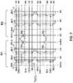
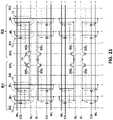
- the present inventionis an array architecture that provides the ability not only to erase just a segment of the row of memory cell pairs 11 , but also just a single row of memory cells 10 in that segment.
- FIG. 3illustrates a first embodiment for the memory cell pairs 11 of memory cells 10 of FIG. 1 .
- the architecture of FIG. 3is similar to the architecture of FIG. 2 .
- each row of memory cell pairs 11includes a plurality of sub source lines SSL, where each sub source line SSL only extends across and electrically connects together a subset of the source regions for each row of memory cell pairs 11 (i.e., a subrow of memory cell pairs 11 ).
- the rows of memory cell pairs 11are divided up into regions R (i.e., distinct pluralities of the columns of the memory cells), where each sub source line SSL only extends across and electrically connects together the source regions for that portion of the row of memory cell pairs 11 inside of the one region R.
- regions Ri.e., distinct pluralities of the columns of the memory cells
- each region Rbeing two memory cells 10 wide (i.e., two columns wide, with each subrow of memory cells includes two memory cells 10 , and therefore each subrow of memory cell pairs 11 includes four memory cells 10 ).
- the number of regions R and their widthsi.e., the number of columns of memory cells 10 in the region R
- each subrow of memory cells 10 within a region Rcan include enough memory cells to store one byte (8 bits) of data.
- the subrow of memory cells 10 within a region Rcan include enough memory cells to store one word of data (16 or 32 bits).
- the number of rows of memory cell pairs 11 in the memory arraycan vary as needed.
- Each subrow of memory cell pairs 11 within any given region Rhas its own sub source line SSL. Therefore, each region R has its own set of sub source lines SSL.
- Each row of memory cell pairs 11also has its own source line SL extending in the row direction and extending across all the regions R.
- Each sub source line SSL in any given row of memory cell pairs 11is connected to its source line SL by a respective select transistor 34 (i.e., the source/drain channel path of the select transistor 34 is connected between the sub source line SSL and source line SL).
- Each column of select transistors 34is operated by a select transistor line STL (i.e., the select transistor line STL is connected to the gates of the respective select transistors 34 ) that is used to activate (i.e., make the source/drain channel paths conductive to electrically connect the SSLs to the SL's) or deactivate (i.e. make the source/drain channel paths non-conductive to electrically disconnect the SSL's from the SL's) the column of select transistors 34 connected thereto.
- the select transistors 34are activated by applying a voltage on the select transistor line STL that exceeds the threshold voltage of the transistors 34 .
- the transistors 34are deactivated by applying no or zero voltage, or a low voltage below the threshold voltage of the transistors 34 . Therefore, for any given row of memory cell pairs 11 , the sub source lines SSL in that row are electrically isolated from their source line SL and from the other sub source lines SSL in that row when all the select transistors 34 in that row are deactivated.
- the array architecture in FIG. 3also includes erase gate lines EG that extend primarily in the column direction instead of the row direction as shown in FIG. 2 , but also extend in the row direction where each erase gate line EG electrically connects together all the erase gates 30 in one, and only one, of the regions R. So, for example, the erase gate line EG for region R 1 electrically connects together all of the erase gates 30 in region R 1 (i.e., the erase gates 30 for all the subrows of memory cell pairs 11 in region R 1 ), but is electrically isolated from the erase gates 30 for memory cells in the other regions R.
- FIG. 4illustrates exemplary voltages that can be applied to the memory array of FIG. 3 to erase just one of the subrows of memory cells 10 .
- 0Vis applied to all the bit lines BL, all the word lines WL, and all the source lines SL.
- a high positive voltage HV(e.g.
- 0V or a low positive voltage LVe.g., less than 3V
- 0Vis applied to CG 1
- a positive inhibit voltage VCGinhe.g. greater than about 5V
- 0V or a low positive voltage LVe.g., less than 3V
- STL 0is applied to all the other select transistor lines STL.
- the other memory cells 10 in the same row as the target memory cells TMCsare not erased because no high voltage is applied to their erase gates.
- the other memory cells in the same columns as the target memory cells TMCsare not erased because the inhibit voltage VCGinh applied to their control gates is high enough to inhibit any tunneling to the erase gate, yet is not high enough to cause any tunneling to the control gate (because the floating gate will see positive voltages on multiple sides thereof thus no erasure will occur to just one side or corner edge).
- a negative voltagee.g. ⁇ HV
- FIG. 5illustrates exemplary voltages for programming one of the TMCs (right hand memory cell 10 of the TMCs).
- the voltage MV applied to STL 0is greater than the threshold voltage of the select transistors 34 , so applying MV to SL 0 turns on the select transistors 34 in region R 1 (so that all the sub source lines SSL in region 1 are coupled to their respective source lines SL).
- a zero voltageis applied to STL 1 , so the select transistors 34 in region R 2 remain turned off.
- word line WLe.g., LV
- control gate line CGe.g., HV
- erase gate line EGe.g., MV
- sub source line SSLe.g., MV
- bit line BLe.g., Idp
- FIG. 6illustrates an alternate combination of exemplary voltages for programming one of the TMCs (right hand memory cell 10 of the TMCs), which is the same as those shown in FIG. 5 except a high voltage (HV) is applied to EG 0 and inhibit positive voltages VCGinh are applied to the control gate lines CG for non-target memory cells.
- HVhigh voltage
- FIG. 7illustrates exemplary voltages for reading one of the TMCs (right hand memory cell 10 of the TMCs). Only the targeted memory cell receives the requisite read voltage combination as described above on its word line WL (e.g., LV), control gate line CG (e.g., LV), erase gate line EG (e.g., 0V or LV), sub source line SSL (e.g., 0V) and/or bit line BL (e.g., LV).
- Table 1summarizes the exemplary, non-limiting, voltages as indicated in the figures for all the various embodiments herein:
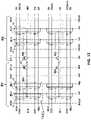
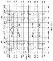
- FIGS. 8-13illustrate a second embodiment, which is similar to the embodiment of FIGS. 3-7 , except that separate erase gates 30 are formed for each memory cell 10 in the pair of memory cells 11 (i.e., each of the memory cells 10 sharing a common source region 14 has its own erase gate 30 ) as shown in FIG. 8 .
- FIG. 9illustrates the memory cell array architecture for the memory cell pair configuration of FIG. 8 , which is the same as that shown in FIG. 3 except that each region R of memory cells 10 includes two erase gate lines EG instead of one.
- one erase gate line EGelectrically connects together all the erase gates 30 in the odd rows of memory cells 10
- the other erase gate line EGelectrically connects together all the erase gates 30 in the even rows of memory cells 10 , for that region R.
- the two erase gates 30are connect to different erase gate lines EG.
- FIG. 10illustrates exemplary voltages for erasing all the memory cells 10 on word line WL 1 in region R 1 (i.e., TMCs, because only those cells are subjected to a high erase gate line voltage without a countering positive control gate line inhibit voltage).
- a negative voltagee.g. ⁇ HV
- FIGS. 11 and 12illustrate two different exemplary voltage combinations for programming one of the memory cells 10 (right hand cell of the TMCs).
- FIG. 13illustrates exemplary voltages for reading one of the memory cells 10 (right hand cell of the TMCs).
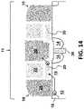
- FIGS. 14-19illustrate a third embodiment, which is similar to the embodiment of FIGS. 3-7 , except that for each memory cell pair 11 , a separate source region 14 is formed for each of the two memory cells 10 (i.e., each of the memory cells 10 sharing a common erase gate 30 has its own source region 14 isolated from the other source region 14 for the other memory cell 10 ) as shown in FIG. 14 .
- the source regions 14are separated by STI 36 (shallow trench isolation such as oxide).
- FIG. 15illustrates the memory cell array architecture for the memory cell configuration of FIG. 14 , which is the same as that shown in FIG.
- each individual subrow of memory cells 10 in each region Rincludes its own sub source line SSL and select transistor 34 , and each row of memory cells 10 extending across all the regions R includes its own source line SL (compared to sharing a sub source line SSL, select transistor 34 , and source line SL between two adjacent rows of memory cells 10 —one row of memory cell pairs 11 ).
- each row of memory cells 10 extending across all the regions Rincludes its own source line SL (compared to sharing a sub source line SSL, select transistor 34 , and source line SL between two adjacent rows of memory cells 10 —one row of memory cell pairs 11 ).
- FIG. 16illustrates exemplary voltages for erasing all the memory cells on word line WL 1 in region R 1 (i.e., TMCs, because only those memory cells are subjected to a high erase gate line voltage without a countering positive control gate line inhibit voltage).
- a negative voltagee.g. ⁇ HV
- FIGS. 17 and 18illustrate two different exemplary voltage combinations for programming one of the memory cells 10 (right hand cell of the TMCs).
- FIG. 19illustrates exemplary voltages for reading one of the memory cells 10 (right hand cell of the TMCs).
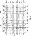
- FIGS. 20-25illustrate a fourth embodiment, which is similar to the embodiment of FIGS. 3-7 , except that for each memory cell pair 11 , a separate source region 14 is formed for each of the two memory cells 10 (i.e., each of the memory cells 10 has its own source region 14 isolated from the other source region 14 for the other memory cell 10 ), and that separate erase gates 30 are formed for each memory cell 10 in the pair of memory cells 11 (i.e., each of the memory cells 10 has its own erase gate 30 isolated from the other erase gate 30 for the other memory cell) as shown in FIG. 20 .
- the source regions 14are separated by STI 36 (shallow trench isolation such as oxide).
- FIG. 21illustrates the memory cell array architecture for the memory cell configuration of FIG.
- each individual subrow of memory cells 10 in each region Rincludes its own sub source line SSL and select transistor 34 , and each row of memory cells 10 extending across all the regions R includes its own source line SL (compared to sharing a sub source line SSL, select transistor 34 , and source line SL between two adjacent rows of memory cells 10 —one row of memory cell pairs 11 ), and (2) that each region R of memory cells 10 includes two erase gate lines EG instead of one (i.e., for each region R, one erase gate line EG electrically connects together all the erase gates 30 in the odd rows of memory cells 10 , and the other erase gate line EG electrically connects together all the erase gates 30 in the even rows of memory cells 10 , for that region R).
- FIG. 22illustrates exemplary voltages for erasing all the memory cells on word line WL 1 in region R 1 (i.e., TMCs, because only those memory cells are subjected to a high erase gate line voltage without a countering positive control gate line inhibit voltage).
- a negative voltagee.g., ⁇ HV
- FIGS. 23 and 24illustrate two different exemplary voltage combinations for programming one of the memory cells 10 (right hand cell of the TMCs).
- FIG. 25illustrates exemplary voltages for reading one of the memory cells 10 (right hand cell of the TMCs).
- the architecture of an exemplary memory deviceis illustrated in FIG. 26 .
- the memory deviceincludes an array 50 of the non-volatile memory cells 10 , which can be segregated into two separate planes (Plane A 52 a and Plane B 52 b ).
- the memory cells 10can be of the type shown in FIGS. 1, 8, 14 and 20 formed on a single chip, arranged in a plurality of rows and columns in the semiconductor substrate 12 as depicted in FIGS. 3-7, 9-13, 15-19 and 21-25 .
- Adjacent to the array of non-volatile memory cellsare address decoders, such as low voltage LV row decoder (e.g., XDEC 54 ), source line driver (e.g.
- SLDRV 56column decoder
- YMUX 58high voltage row decoder
- HVDEC 60high voltage row decoder
- BLINHCTL 62bit line controller
- Column decoder 58includes a sense amplifier containing circuitry for measuring the currents on the bit lines during a read operation.
- Controller 66(containing control circuitry) controls the various device elements to implement each operation (program, erase, read) on target memory cells, including the peripheral circuits mentioned above as well as the select transistors 34 inside the memory array, to provide the signals on the various lines including the select transistor lines STL.
- Charge pump CHRGPMP 64provides the various voltages used to read, program and erase the memory cells under the control of the controller 66 .
- Controller 66is configured to operate the memory device to program, erase and read the memory cells 10 .
- the total size of the arrayis only moderately increased (to make room for the select transistors and their lines), which is a worthwhile tradeoff for being able to erase only a single sub row of memory cells 10 at any given time, and selectively apply voltages only on certain sub source lines SSL during operation to increase performance.
- the select transistorscan be added to the memory array without otherwise materially changing the remaining portions of the memory array and the process flow in forming it.
- applying a 0Vis the same as applying no voltage or grounding the line where the result is zero volts on the particular line.
- applying a low positive or negative voltage for one or more of the indicated linescan produce the same desired results for programming, reading and erasing the memory cells.
- adjacentincludes “directly adjacent” (no intermediate materials, elements or space disposed there between) and “indirectly adjacent” (intermediate materials, elements or space disposed there between)
- mounted toincludes “directly mounted to” (no intermediate materials, elements or space disposed there between) and “indirectly mounted to” (intermediate materials, elements or spaced disposed there between)
- electrically coupledincludes “directly electrically coupled to” (no intermediate materials or elements there between that electrically connect the elements together) and “indirectly electrically coupled to” (intermediate materials or elements there between that electrically connect the elements together).
- forming an element “over a substrate”can include forming the element directly on the substrate with no intermediate materials/elements there between, as well as forming the element indirectly on the substrate with one or more intermediate materials/elements there between.
Landscapes
- Engineering & Computer Science (AREA)
- Microelectronics & Electronic Packaging (AREA)
- Non-Volatile Memory (AREA)
- Semiconductor Memories (AREA)
- Read Only Memory (AREA)
Abstract
Description
| TABLE 1 | ||||
| LV | <3 | V | ||
| HV | >7 | V | ||
| VCGinh | >5 | V | ||
| MV | 3 V < MV < 7 V |
| Idp | 1-3 | uA | ||
Claims (20)
Priority Applications (7)
| Application Number | Priority Date | Filing Date | Title |
|---|---|---|---|
| US16/784,183US11315636B2 (en) | 2019-10-14 | 2020-02-06 | Four gate, split-gate flash memory array with byte erase operation |
| JP2022520796AJP7312910B2 (en) | 2019-10-14 | 2020-03-12 | Four Gate Split Gate Flash Memory Array with Byte Erase Operation |
| PCT/US2020/022450WO2021076178A1 (en) | 2019-10-14 | 2020-03-12 | Four gate, split-gate flash memory array with byte erase operation |
| CN202080071209.0ACN114616625B (en) | 2019-10-14 | 2020-03-12 | Four-gate split-gate flash memory array with byte erase operation |
| EP20718030.8AEP4046158B1 (en) | 2019-10-14 | 2020-03-12 | Four gate, split-gate flash memory array with byte erase operation |
| KR1020227009644AKR102743578B1 (en) | 2019-10-14 | 2020-03-12 | 4-gate, split-gate flash memory array with byte erase operation |
| TW109134882ATWI759900B (en) | 2019-10-14 | 2020-10-08 | Four gate, split-gate flash memory array with byte erase operation |
Applications Claiming Priority (2)
| Application Number | Priority Date | Filing Date | Title |
|---|---|---|---|
| US201962914799P | 2019-10-14 | 2019-10-14 | |
| US16/784,183US11315636B2 (en) | 2019-10-14 | 2020-02-06 | Four gate, split-gate flash memory array with byte erase operation |
Publications (2)
| Publication Number | Publication Date |
|---|---|
| US20210110873A1 US20210110873A1 (en) | 2021-04-15 |
| US11315636B2true US11315636B2 (en) | 2022-04-26 |
Family
ID=75383806
Family Applications (1)
| Application Number | Title | Priority Date | Filing Date |
|---|---|---|---|
| US16/784,183ActiveUS11315636B2 (en) | 2019-10-14 | 2020-02-06 | Four gate, split-gate flash memory array with byte erase operation |
Country Status (7)
| Country | Link |
|---|---|
| US (1) | US11315636B2 (en) |
| EP (1) | EP4046158B1 (en) |
| JP (1) | JP7312910B2 (en) |
| KR (1) | KR102743578B1 (en) |
| CN (1) | CN114616625B (en) |
| TW (1) | TWI759900B (en) |
| WO (1) | WO2021076178A1 (en) |
Families Citing this family (6)
| Publication number | Priority date | Publication date | Assignee | Title |
|---|---|---|---|---|
| US11742024B2 (en)* | 2020-05-27 | 2023-08-29 | Taiwan Semiconductor Manufacturing Company Limited | Memory device comprising source line coupled to multiple memory cells and method of operation |
| US11972800B2 (en)* | 2021-12-16 | 2024-04-30 | Ememory Technology Inc. | Non-volatile memory cell and non-volatile memory cell array |
| US12125523B2 (en)* | 2022-01-27 | 2024-10-22 | Taiwan Semiconductor Manufacturing Company, Ltd. | Memory device and method of manufacturing the same |
| CN115331722A (en)* | 2022-08-23 | 2022-11-11 | 北京知存科技有限公司 | Flash memory chip and programming method and testing method thereof |
| US12131794B2 (en)* | 2022-08-23 | 2024-10-29 | Micron Technology, Inc. | Structures for word line multiplexing in three-dimensional memory arrays |
| JP7660153B2 (en)* | 2023-02-15 | 2025-04-10 | ウィンボンド エレクトロニクス コーポレーション | Flash memory |
Citations (17)
| Publication number | Priority date | Publication date | Assignee | Title |
|---|---|---|---|---|
| US5029130A (en) | 1990-01-22 | 1991-07-02 | Silicon Storage Technology, Inc. | Single transistor non-valatile electrically alterable semiconductor memory device |
| US6181607B1 (en)* | 1999-04-22 | 2001-01-30 | Aplus Flash Technology, Inc. | Reversed split-gate cell array |
| US20020176286A1 (en) | 2000-10-30 | 2002-11-28 | Virtual Silicon Technology, Inc. | Common source EEPROM and flash memory |
| US20030206455A1 (en) | 2001-04-23 | 2003-11-06 | Aplus Flash Technology, Inc. | Novel flash memory array structure suitable for multiple simultaneous operations |
| US6741501B2 (en)* | 2001-11-30 | 2004-05-25 | Renesas Technology Corporation | Nonvolatile semiconductor memory device and manufacturing method thereof |
| US20070047302A1 (en) | 2002-07-05 | 2007-03-01 | Aplus Flash Technology, Inc. | Novel monolithic, combo nonvolatile memory allowing byte, page and block write with no disturb and divided-well in the cell array using a unified cell structure and technology with a new scheme of decoder and layout |
| US7608882B2 (en) | 2003-08-11 | 2009-10-27 | Macronix International Co., Ltd. | Split-gate non-volatile memory |
| US20090279361A1 (en) | 2008-05-06 | 2009-11-12 | Atmel Corporation | Addressable Memory Array |
| US7868375B2 (en) | 2007-08-06 | 2011-01-11 | Silicon Storage Technology, Inc. | Split gate non-volatile flash memory cell having a floating gate, control gate, select gate and an erase gate with an overhang over the floating gate, array and method of manufacturing |
| US8237212B2 (en)* | 2002-07-05 | 2012-08-07 | Abedneja Assetts AG L.L.C. | Nonvolatile memory with a unified cell structure |
| US20130223148A1 (en)* | 2012-02-28 | 2013-08-29 | Samsung Electronics Co., Ltd. | Nonvolatile memory device and embedded memory system including the same |
| US20160042790A1 (en) | 2014-08-08 | 2016-02-11 | Silicon Storage Technology, Inc. | Flash Memory System With EEPROM Functionality |
| US9443594B2 (en)* | 2013-11-11 | 2016-09-13 | Samsung Electronics Co., Ltd. | Logic embedded nonvolatile memory device |
| TWI625843B (en) | 2016-05-18 | 2018-06-01 | 超捷公司 | Method for manufacturing split gate non-electricity flash memory cell |
| US10269440B2 (en) | 2016-05-17 | 2019-04-23 | Silicon Storage Technology, Inc. | Flash memory array with individual memory cell read, program and erase |
| US20190355424A1 (en) | 2018-05-16 | 2019-11-21 | Silicon Storage Technology, Inc. | Split-Gate Flash Memory Array With Byte Erase Operation |
| US10812084B2 (en)* | 2018-11-06 | 2020-10-20 | The Regents Of The University Of California | Reconfigurable physically unclonable functions based on analog non-volatile memories |
Family Cites Families (8)
| Publication number | Priority date | Publication date | Assignee | Title |
|---|---|---|---|---|
| KR960000616B1 (en)* | 1993-01-13 | 1996-01-10 | 삼성전자주식회사 | Nonvolatile Semiconductor Memory Device |
| JP4899241B2 (en)* | 1999-12-06 | 2012-03-21 | ソニー株式会社 | Nonvolatile semiconductor memory device and operation method thereof |
| US6747310B2 (en)* | 2002-10-07 | 2004-06-08 | Actrans System Inc. | Flash memory cells with separated self-aligned select and erase gates, and process of fabrication |
| US7247907B2 (en)* | 2005-05-20 | 2007-07-24 | Silicon Storage Technology, Inc. | Bidirectional split gate NAND flash memory structure and array, method of programming, erasing and reading thereof, and method of manufacturing |
| JP2012119013A (en)* | 2010-11-29 | 2012-06-21 | Toshiba Corp | Nonvolatile semiconductor memory device |
| US8811093B2 (en)* | 2012-03-13 | 2014-08-19 | Silicon Storage Technology, Inc. | Non-volatile memory device and a method of operating same |
| US9123822B2 (en)* | 2013-08-02 | 2015-09-01 | Silicon Storage Technology, Inc. | Split gate non-volatile flash memory cell having a silicon-metal floating gate and method of making same |
| CN109328385B (en)* | 2016-05-17 | 2023-03-21 | 硅存储技术公司 | Memory cell array with individual memory cell reading, programming and erasing |
- 2020
- 2020-02-06USUS16/784,183patent/US11315636B2/enactiveActive
- 2020-03-12CNCN202080071209.0Apatent/CN114616625B/enactiveActive
- 2020-03-12KRKR1020227009644Apatent/KR102743578B1/enactiveActive
- 2020-03-12WOPCT/US2020/022450patent/WO2021076178A1/ennot_activeCeased
- 2020-03-12JPJP2022520796Apatent/JP7312910B2/enactiveActive
- 2020-03-12EPEP20718030.8Apatent/EP4046158B1/enactiveActive
- 2020-10-08TWTW109134882Apatent/TWI759900B/enactive
Patent Citations (18)
| Publication number | Priority date | Publication date | Assignee | Title |
|---|---|---|---|---|
| US5029130A (en) | 1990-01-22 | 1991-07-02 | Silicon Storage Technology, Inc. | Single transistor non-valatile electrically alterable semiconductor memory device |
| US6181607B1 (en)* | 1999-04-22 | 2001-01-30 | Aplus Flash Technology, Inc. | Reversed split-gate cell array |
| US20020176286A1 (en) | 2000-10-30 | 2002-11-28 | Virtual Silicon Technology, Inc. | Common source EEPROM and flash memory |
| US20030206455A1 (en) | 2001-04-23 | 2003-11-06 | Aplus Flash Technology, Inc. | Novel flash memory array structure suitable for multiple simultaneous operations |
| US6741501B2 (en)* | 2001-11-30 | 2004-05-25 | Renesas Technology Corporation | Nonvolatile semiconductor memory device and manufacturing method thereof |
| US20070047302A1 (en) | 2002-07-05 | 2007-03-01 | Aplus Flash Technology, Inc. | Novel monolithic, combo nonvolatile memory allowing byte, page and block write with no disturb and divided-well in the cell array using a unified cell structure and technology with a new scheme of decoder and layout |
| US8237212B2 (en)* | 2002-07-05 | 2012-08-07 | Abedneja Assetts AG L.L.C. | Nonvolatile memory with a unified cell structure |
| US7608882B2 (en) | 2003-08-11 | 2009-10-27 | Macronix International Co., Ltd. | Split-gate non-volatile memory |
| US7868375B2 (en) | 2007-08-06 | 2011-01-11 | Silicon Storage Technology, Inc. | Split gate non-volatile flash memory cell having a floating gate, control gate, select gate and an erase gate with an overhang over the floating gate, array and method of manufacturing |
| US20090279361A1 (en) | 2008-05-06 | 2009-11-12 | Atmel Corporation | Addressable Memory Array |
| US20130223148A1 (en)* | 2012-02-28 | 2013-08-29 | Samsung Electronics Co., Ltd. | Nonvolatile memory device and embedded memory system including the same |
| US9443594B2 (en)* | 2013-11-11 | 2016-09-13 | Samsung Electronics Co., Ltd. | Logic embedded nonvolatile memory device |
| US20160042790A1 (en) | 2014-08-08 | 2016-02-11 | Silicon Storage Technology, Inc. | Flash Memory System With EEPROM Functionality |
| US9286982B2 (en) | 2014-08-08 | 2016-03-15 | Silicon Storage Technology, Inc. | Flash memory system with EEPROM functionality |
| US10269440B2 (en) | 2016-05-17 | 2019-04-23 | Silicon Storage Technology, Inc. | Flash memory array with individual memory cell read, program and erase |
| TWI625843B (en) | 2016-05-18 | 2018-06-01 | 超捷公司 | Method for manufacturing split gate non-electricity flash memory cell |
| US20190355424A1 (en) | 2018-05-16 | 2019-11-21 | Silicon Storage Technology, Inc. | Split-Gate Flash Memory Array With Byte Erase Operation |
| US10812084B2 (en)* | 2018-11-06 | 2020-10-20 | The Regents Of The University Of California | Reconfigurable physically unclonable functions based on analog non-volatile memories |
Non-Patent Citations (1)
| Title |
|---|
| Taiwanese Office Action dated Jul. 26, 2021 corresponding to the related Taiwanese Patent Application No. 11020712920. |
Also Published As
| Publication number | Publication date |
|---|---|
| CN114616625B (en) | 2024-12-17 |
| CN114616625A (en) | 2022-06-10 |
| KR102743578B1 (en) | 2024-12-16 |
| JP2022551851A (en) | 2022-12-14 |
| EP4046158B1 (en) | 2023-08-30 |
| KR20220047869A (en) | 2022-04-19 |
| US20210110873A1 (en) | 2021-04-15 |
| TWI759900B (en) | 2022-04-01 |
| WO2021076178A1 (en) | 2021-04-22 |
| EP4046158A1 (en) | 2022-08-24 |
| TW202139200A (en) | 2021-10-16 |
| JP7312910B2 (en) | 2023-07-21 |
Similar Documents
| Publication | Publication Date | Title |
|---|---|---|
| US10460811B2 (en) | Array of three-gate flash memory cells with individual memory cell read, program and erase | |
| US11315636B2 (en) | Four gate, split-gate flash memory array with byte erase operation | |
| US10388389B2 (en) | Flash memory array with individual memory cell read, program and erase | |
| US10607703B2 (en) | Split-gate flash memory array with byte erase operation | |
| EP3459114B1 (en) | Array of three-gate flash memory cells with individual memory cell read, program and erase | |
| US5852577A (en) | Electrically erasable and programmable read-only memory having a small unit for program and erase |
Legal Events
| Date | Code | Title | Description |
|---|---|---|---|
| AS | Assignment | Owner name:SILICON STORAGE TECHNOLOGY, INC., CALIFORNIA Free format text:ASSIGNMENT OF ASSIGNORS INTEREST;ASSIGNORS:LIANG, HSUAN;WU, MAN-TANG;YANG, JENG-WEI;AND OTHERS;SIGNING DATES FROM 20200205 TO 20200206;REEL/FRAME:051746/0756 | |
| FEPP | Fee payment procedure | Free format text:ENTITY STATUS SET TO UNDISCOUNTED (ORIGINAL EVENT CODE: BIG.); ENTITY STATUS OF PATENT OWNER: LARGE ENTITY | |
| AS | Assignment | Owner name:JPMORGAN CHASE BANK, N.A., AS ADMINISTRATIVE AGENT, DELAWARE Free format text:SECURITY INTEREST;ASSIGNORS:MICROCHIP TECHNOLOGY INC.;SILICON STORAGE TECHNOLOGY, INC.;ATMEL CORPORATION;AND OTHERS;REEL/FRAME:053311/0305 Effective date:20200327 | |
| AS | Assignment | Owner name:SILICON STORAGE TECHNOLOGY, INC., ARIZONA Free format text:RELEASE BY SECURED PARTY;ASSIGNOR:JPMORGAN CHASE BANK, N.A, AS ADMINISTRATIVE AGENT;REEL/FRAME:053466/0011 Effective date:20200529 Owner name:ATMEL CORPORATION, ARIZONA Free format text:RELEASE BY SECURED PARTY;ASSIGNOR:JPMORGAN CHASE BANK, N.A, AS ADMINISTRATIVE AGENT;REEL/FRAME:053466/0011 Effective date:20200529 Owner name:MICROSEMI STORAGE SOLUTIONS, INC., ARIZONA Free format text:RELEASE BY SECURED PARTY;ASSIGNOR:JPMORGAN CHASE BANK, N.A, AS ADMINISTRATIVE AGENT;REEL/FRAME:053466/0011 Effective date:20200529 Owner name:MICROCHIP TECHNOLOGY INC., ARIZONA Free format text:RELEASE BY SECURED PARTY;ASSIGNOR:JPMORGAN CHASE BANK, N.A, AS ADMINISTRATIVE AGENT;REEL/FRAME:053466/0011 Effective date:20200529 Owner name:MICROSEMI CORPORATION, CALIFORNIA Free format text:RELEASE BY SECURED PARTY;ASSIGNOR:JPMORGAN CHASE BANK, N.A, AS ADMINISTRATIVE AGENT;REEL/FRAME:053466/0011 Effective date:20200529 | |
| AS | Assignment | Owner name:JPMORGAN CHASE BANK, N.A., AS ADMINISTRATIVE AGENT, ILLINOIS Free format text:SECURITY INTEREST;ASSIGNORS:MICROCHIP TECHNOLOGY INC.;SILICON STORAGE TECHNOLOGY, INC.;ATMEL CORPORATION;AND OTHERS;REEL/FRAME:052856/0909 Effective date:20200529 Owner name:WELLS FARGO BANK, NATIONAL ASSOCIATION, MINNESOTA Free format text:SECURITY INTEREST;ASSIGNORS:MICROCHIP TECHNOLOGY INC.;SILICON STORAGE TECHNOLOGY, INC.;ATMEL CORPORATION;AND OTHERS;REEL/FRAME:053468/0705 Effective date:20200529 | |
| AS | Assignment | Owner name:WELLS FARGO BANK, NATIONAL ASSOCIATION, AS COLLATERAL AGENT, MINNESOTA Free format text:SECURITY INTEREST;ASSIGNORS:MICROCHIP TECHNOLOGY INCORPORATED;SILICON STORAGE TECHNOLOGY, INC.;ATMEL CORPORATION;AND OTHERS;REEL/FRAME:055671/0612 Effective date:20201217 | |
| AS | Assignment | Owner name:WELLS FARGO BANK, NATIONAL ASSOCIATION, AS NOTES COLLATERAL AGENT, MINNESOTA Free format text:SECURITY INTEREST;ASSIGNORS:MICROCHIP TECHNOLOGY INCORPORATED;SILICON STORAGE TECHNOLOGY, INC.;ATMEL CORPORATION;AND OTHERS;REEL/FRAME:057935/0474 Effective date:20210528 | |
| STPP | Information on status: patent application and granting procedure in general | Free format text:DOCKETED NEW CASE - READY FOR EXAMINATION | |
| STPP | Information on status: patent application and granting procedure in general | Free format text:NON FINAL ACTION MAILED | |
| STPP | Information on status: patent application and granting procedure in general | Free format text:RESPONSE TO NON-FINAL OFFICE ACTION ENTERED AND FORWARDED TO EXAMINER | |
| AS | Assignment | Owner name:WELLS FARGO BANK, NATIONAL ASSOCIATION, AS NOTES COLLATERAL AGENT, MINNESOTA Free format text:GRANT OF SECURITY INTEREST IN PATENT RIGHTS;ASSIGNORS:MICROCHIP TECHNOLOGY INCORPORATED;SILICON STORAGE TECHNOLOGY, INC.;ATMEL CORPORATION;AND OTHERS;REEL/FRAME:058214/0625 Effective date:20211117 | |
| STPP | Information on status: patent application and granting procedure in general | Free format text:FINAL REJECTION MAILED | |
| STPP | Information on status: patent application and granting procedure in general | Free format text:NOTICE OF ALLOWANCE MAILED -- APPLICATION RECEIVED IN OFFICE OF PUBLICATIONS | |
| AS | Assignment | Owner name:MICROSEMI STORAGE SOLUTIONS, INC., ARIZONA Free format text:RELEASE BY SECURED PARTY;ASSIGNOR:JPMORGAN CHASE BANK, N.A., AS ADMINISTRATIVE AGENT;REEL/FRAME:059263/0001 Effective date:20220218 Owner name:MICROSEMI CORPORATION, ARIZONA Free format text:RELEASE BY SECURED PARTY;ASSIGNOR:JPMORGAN CHASE BANK, N.A., AS ADMINISTRATIVE AGENT;REEL/FRAME:059263/0001 Effective date:20220218 Owner name:ATMEL CORPORATION, ARIZONA Free format text:RELEASE BY SECURED PARTY;ASSIGNOR:JPMORGAN CHASE BANK, N.A., AS ADMINISTRATIVE AGENT;REEL/FRAME:059263/0001 Effective date:20220218 Owner name:SILICON STORAGE TECHNOLOGY, INC., ARIZONA Free format text:RELEASE BY SECURED PARTY;ASSIGNOR:JPMORGAN CHASE BANK, N.A., AS ADMINISTRATIVE AGENT;REEL/FRAME:059263/0001 Effective date:20220218 Owner name:MICROCHIP TECHNOLOGY INCORPORATED, ARIZONA Free format text:RELEASE BY SECURED PARTY;ASSIGNOR:JPMORGAN CHASE BANK, N.A., AS ADMINISTRATIVE AGENT;REEL/FRAME:059263/0001 Effective date:20220218 | |
| AS | Assignment | Owner name:MICROSEMI STORAGE SOLUTIONS, INC., ARIZONA Free format text:RELEASE BY SECURED PARTY;ASSIGNOR:WELLS FARGO BANK, NATIONAL ASSOCIATION, AS NOTES COLLATERAL AGENT;REEL/FRAME:059358/0335 Effective date:20220228 Owner name:MICROSEMI CORPORATION, ARIZONA Free format text:RELEASE BY SECURED PARTY;ASSIGNOR:WELLS FARGO BANK, NATIONAL ASSOCIATION, AS NOTES COLLATERAL AGENT;REEL/FRAME:059358/0335 Effective date:20220228 Owner name:ATMEL CORPORATION, ARIZONA Free format text:RELEASE BY SECURED PARTY;ASSIGNOR:WELLS FARGO BANK, NATIONAL ASSOCIATION, AS NOTES COLLATERAL AGENT;REEL/FRAME:059358/0335 Effective date:20220228 Owner name:SILICON STORAGE TECHNOLOGY, INC., ARIZONA Free format text:RELEASE BY SECURED PARTY;ASSIGNOR:WELLS FARGO BANK, NATIONAL ASSOCIATION, AS NOTES COLLATERAL AGENT;REEL/FRAME:059358/0335 Effective date:20220228 Owner name:MICROCHIP TECHNOLOGY INCORPORATED, ARIZONA Free format text:RELEASE BY SECURED PARTY;ASSIGNOR:WELLS FARGO BANK, NATIONAL ASSOCIATION, AS NOTES COLLATERAL AGENT;REEL/FRAME:059358/0335 Effective date:20220228 | |
| AS | Assignment | Owner name:MICROSEMI STORAGE SOLUTIONS, INC., ARIZONA Free format text:RELEASE BY SECURED PARTY;ASSIGNOR:WELLS FARGO BANK, NATIONAL ASSOCIATION, AS NOTES COLLATERAL AGENT;REEL/FRAME:059863/0400 Effective date:20220228 Owner name:MICROSEMI CORPORATION, ARIZONA Free format text:RELEASE BY SECURED PARTY;ASSIGNOR:WELLS FARGO BANK, NATIONAL ASSOCIATION, AS NOTES COLLATERAL AGENT;REEL/FRAME:059863/0400 Effective date:20220228 Owner name:ATMEL CORPORATION, ARIZONA Free format text:RELEASE BY SECURED PARTY;ASSIGNOR:WELLS FARGO BANK, NATIONAL ASSOCIATION, AS NOTES COLLATERAL AGENT;REEL/FRAME:059863/0400 Effective date:20220228 Owner name:SILICON STORAGE TECHNOLOGY, INC., ARIZONA Free format text:RELEASE BY SECURED PARTY;ASSIGNOR:WELLS FARGO BANK, NATIONAL ASSOCIATION, AS NOTES COLLATERAL AGENT;REEL/FRAME:059863/0400 Effective date:20220228 Owner name:MICROCHIP TECHNOLOGY INCORPORATED, ARIZONA Free format text:RELEASE BY SECURED PARTY;ASSIGNOR:WELLS FARGO BANK, NATIONAL ASSOCIATION, AS NOTES COLLATERAL AGENT;REEL/FRAME:059863/0400 Effective date:20220228 | |
| AS | Assignment | Owner name:MICROSEMI STORAGE SOLUTIONS, INC., ARIZONA Free format text:RELEASE BY SECURED PARTY;ASSIGNOR:WELLS FARGO BANK, NATIONAL ASSOCIATION, AS NOTES COLLATERAL AGENT;REEL/FRAME:059363/0001 Effective date:20220228 Owner name:MICROSEMI CORPORATION, ARIZONA Free format text:RELEASE BY SECURED PARTY;ASSIGNOR:WELLS FARGO BANK, NATIONAL ASSOCIATION, AS NOTES COLLATERAL AGENT;REEL/FRAME:059363/0001 Effective date:20220228 Owner name:ATMEL CORPORATION, ARIZONA Free format text:RELEASE BY SECURED PARTY;ASSIGNOR:WELLS FARGO BANK, NATIONAL ASSOCIATION, AS NOTES COLLATERAL AGENT;REEL/FRAME:059363/0001 Effective date:20220228 Owner name:SILICON STORAGE TECHNOLOGY, INC., ARIZONA Free format text:RELEASE BY SECURED PARTY;ASSIGNOR:WELLS FARGO BANK, NATIONAL ASSOCIATION, AS NOTES COLLATERAL AGENT;REEL/FRAME:059363/0001 Effective date:20220228 Owner name:MICROCHIP TECHNOLOGY INCORPORATED, ARIZONA Free format text:RELEASE BY SECURED PARTY;ASSIGNOR:WELLS FARGO BANK, NATIONAL ASSOCIATION, AS NOTES COLLATERAL AGENT;REEL/FRAME:059363/0001 Effective date:20220228 | |
| AS | Assignment | Owner name:MICROSEMI STORAGE SOLUTIONS, INC., ARIZONA Free format text:RELEASE BY SECURED PARTY;ASSIGNOR:WELLS FARGO BANK, NATIONAL ASSOCIATION, AS NOTES COLLATERAL AGENT;REEL/FRAME:060894/0437 Effective date:20220228 Owner name:MICROSEMI CORPORATION, ARIZONA Free format text:RELEASE BY SECURED PARTY;ASSIGNOR:WELLS FARGO BANK, NATIONAL ASSOCIATION, AS NOTES COLLATERAL AGENT;REEL/FRAME:060894/0437 Effective date:20220228 Owner name:ATMEL CORPORATION, ARIZONA Free format text:RELEASE BY SECURED PARTY;ASSIGNOR:WELLS FARGO BANK, NATIONAL ASSOCIATION, AS NOTES COLLATERAL AGENT;REEL/FRAME:060894/0437 Effective date:20220228 Owner name:SILICON STORAGE TECHNOLOGY, INC., ARIZONA Free format text:RELEASE BY SECURED PARTY;ASSIGNOR:WELLS FARGO BANK, NATIONAL ASSOCIATION, AS NOTES COLLATERAL AGENT;REEL/FRAME:060894/0437 Effective date:20220228 Owner name:MICROCHIP TECHNOLOGY INCORPORATED, ARIZONA Free format text:RELEASE BY SECURED PARTY;ASSIGNOR:WELLS FARGO BANK, NATIONAL ASSOCIATION, AS NOTES COLLATERAL AGENT;REEL/FRAME:060894/0437 Effective date:20220228 | |
| STPP | Information on status: patent application and granting procedure in general | Free format text:PUBLICATIONS -- ISSUE FEE PAYMENT VERIFIED | |
| STCF | Information on status: patent grant | Free format text:PATENTED CASE | |
| MAFP | Maintenance fee payment | Free format text:PAYMENT OF MAINTENANCE FEE, 4TH YEAR, LARGE ENTITY (ORIGINAL EVENT CODE: M1551); ENTITY STATUS OF PATENT OWNER: LARGE ENTITY Year of fee payment:4 |