US11309244B2 - Electrical fuse structure and method of formation - Google Patents
Electrical fuse structure and method of formationDownload PDFInfo
- Publication number
- US11309244B2 US11309244B2US15/863,169US201815863169AUS11309244B2US 11309244 B2US11309244 B2US 11309244B2US 201815863169 AUS201815863169 AUS 201815863169AUS 11309244 B2US11309244 B2US 11309244B2
- Authority
- US
- United States
- Prior art keywords
- cathode
- opening
- layer
- forming
- over
- Prior art date
- Legal status (The legal status is an assumption and is not a legal conclusion. Google has not performed a legal analysis and makes no representation as to the accuracy of the status listed.)
- Active, expires
Links
Images


Classifications
- H—ELECTRICITY
- H01—ELECTRIC ELEMENTS
- H01L—SEMICONDUCTOR DEVICES NOT COVERED BY CLASS H10
- H01L23/00—Details of semiconductor or other solid state devices
- H01L23/52—Arrangements for conducting electric current within the device in operation from one component to another, i.e. interconnections, e.g. wires, lead frames
- H01L23/522—Arrangements for conducting electric current within the device in operation from one component to another, i.e. interconnections, e.g. wires, lead frames including external interconnections consisting of a multilayer structure of conductive and insulating layers inseparably formed on the semiconductor body
- H01L23/525—Arrangements for conducting electric current within the device in operation from one component to another, i.e. interconnections, e.g. wires, lead frames including external interconnections consisting of a multilayer structure of conductive and insulating layers inseparably formed on the semiconductor body with adaptable interconnections
- H01L23/5256—Arrangements for conducting electric current within the device in operation from one component to another, i.e. interconnections, e.g. wires, lead frames including external interconnections consisting of a multilayer structure of conductive and insulating layers inseparably formed on the semiconductor body with adaptable interconnections comprising fuses, i.e. connections having their state changed from conductive to non-conductive
- H—ELECTRICITY
- H01—ELECTRIC ELEMENTS
- H01L—SEMICONDUCTOR DEVICES NOT COVERED BY CLASS H10
- H01L23/00—Details of semiconductor or other solid state devices
- H01L23/52—Arrangements for conducting electric current within the device in operation from one component to another, i.e. interconnections, e.g. wires, lead frames
- H01L23/522—Arrangements for conducting electric current within the device in operation from one component to another, i.e. interconnections, e.g. wires, lead frames including external interconnections consisting of a multilayer structure of conductive and insulating layers inseparably formed on the semiconductor body
- H01L23/5226—Via connections in a multilevel interconnection structure
- H—ELECTRICITY
- H01—ELECTRIC ELEMENTS
- H01L—SEMICONDUCTOR DEVICES NOT COVERED BY CLASS H10
- H01L2924/00—Indexing scheme for arrangements or methods for connecting or disconnecting semiconductor or solid-state bodies as covered by H01L24/00
- H—ELECTRICITY
- H01—ELECTRIC ELEMENTS
- H01L—SEMICONDUCTOR DEVICES NOT COVERED BY CLASS H10
- H01L2924/00—Indexing scheme for arrangements or methods for connecting or disconnecting semiconductor or solid-state bodies as covered by H01L24/00
- H01L2924/0001—Technical content checked by a classifier
- H01L2924/0002—Not covered by any one of groups H01L24/00, H01L24/00 and H01L2224/00
Definitions
- the disclosurerelates generally to a fuse structure and method of forming the fuse structure and, more particularly, to an electrical fuse in a semiconductor device and method of forming the electrical fuse.
- fuse elementsare widely used features in integrated circuits for a variety of purposes, such as in memory repair, analog resistor trimming, and chip identification. For example, by replacing defective memory cells on chips with redundant cells on the same chips, memory manufacturing yields can be significantly increased.
- a fuse disconnected by a laser beamis referred to as a laser fuse, and a fuse disconnected by passing an electrical current, or blowing, is referred to as an electrical fuse, or e-fuse.
- E-fusesmay be incorporated in the design of integrated circuits, wherein the fuses are selectively blown, for example, by passing an electrical current of a sufficient magnitude to cause electro-migration or melting of a fuse link, thereby creating a more resistive path or an open circuit.
- a contact to a cathode of a conventional fusemay cause problems when a large electrical current passes through the fuse. This contact is generally aligned with an axis of a fuse link and nearest to the fuse link and has a very small contact area. Because the contact is nearest to and aligned with the fuse link, the resistance between the fuse link and the contact is much lower than any resistance between the fuse link and any other contacts in the cathode. This low resistance may cause a large proportion of the electrical current to flow through the contact.
- the larger electrical current flowing through the contactmay cause electro-migration of the metal in the contact to the fuse link.
- the electro-migration of the metalthen may cause the fuse link to short circuit again when the large electrical current was intended to create a more resistive path or open circuit.
- This problemis increased after a high temperature storage (HTS) or bake process of the chip. Accordingly, there is a need in the art for a more robust fuse structure to overcome the deficiencies of the prior art.
- a fuse structurecomprises an anode, a cathode, a fuse link interposed between the anode and the cathode, and cathode connectors coupled to the cathode.
- the cathode connectorsare each equivalent to or larger than about two times a minimum feature size of a contact that couples to an active device.
- a fuse structurecomprises an anode, a cathode with connectors coupled to the cathode, and a fuse link coupled between the cathode and the anode.
- a cross-section area of each of the connectorsis equal to or larger than a cross-section area of a connector coupling an active device.
- a fuse structurecomprises a cathode, a fuse link, an anode, a dielectric over the cathode, openings in the dielectric over the cathode, and metal connectors disposed in the openings.
- the fuse linkis coupled between the cathode and the anode.
- the openingsexpose a portion of the cathode, and a cross-sectional area parallel to a top surface of the cathode of each of the openings is greater than a minimum feature size.
- FIG. 1is an electrical fuse structure in accordance with an embodiment
- FIG. 2is an electrical fuse structure in accordance with another embodiment
- FIG. 3is an electrical fuse structure in accordance with a further embodiment
- FIG. 4is an electrical fuse structure in accordance with an additional embodiment
- FIGS. 5A-5Fare an exemplary process to form an electrical fuse structure in accordance with an embodiment.
- FIGS. 6A-6Fare an illustrative process to form an electrical fuse structure in accordance with a further embodiment.
- Embodimentswill be described with respect to an electrical fuse structure in a semiconductor chip. Other embodiments contemplate applications where the use of an electrical fuse structure is desirable.
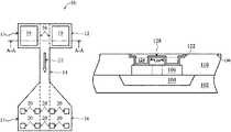
- FIG. 1depicts a fuse structure 10 comprising a cathode 12 , a fuse link 14 , and an anode 16 .
- the fuse structure 10may be formed of a metal, such as copper or the like, or silicided polysilicon, such as nickel silicide (NiSi), titanium silicide (TiSi 2 ), cobalt silicide (CoSi x ), platinum silicide (PtSi 2 ), or the like.
- Cathode 12has a rectangular shaped top surface 13 and has two contacts 18 coupled to the top surface 13 .
- Anode 16has a funnel shaped top surface 17 and has contacts 20 coupled to the top surface 17 .
- the contacts 18 and 20may comprise copper, tungsten, or metals of the like, and may also comprise a diffusion barrier layer lining the contacts 18 and 20 comprising, for example, TiN, TaN, or the like.
- the fuse link 14has a width (perpendicular to arrow 22 ) much smaller than the width of the cathode 12 and the anode 16 . Although the description herein refers to contacts 18 and 20 , these contacts may be vias and/or contacts.
- Contacts 18 in the cathode 12couple a larger surface area of the top surface of the cathode 12 than contacts coupling active devices in other portions of the chip, such as to a transistor gate, and the contacts 18 do not align or intersect a longitudinal axis through the fuse link 14 that is represented by the arrow 22 .
- Some contacts 20 in the anode 16do align or intersect the longitudinal axis through the fuse link 14 .
- dashed lines 26illustrate longitudinal axes along edges of the fuse link 14 that define an area in the cathode 12 , to which no contacts couple, and an area in the anode 16 .
- the contacts 20 in the anode 16may be a contact or via, and may have a surface area width of about 40 nm and a length of about 40 nm.
- the area of contacts 20may be square.
- the contacts 20are said to be of a minimum feature size, which corresponds to the technology node of the embodiment, such as for gate electrodes, contacts, or metal lines.
- a contact sizemay have a critical dimension of between about 15 nm and about 40 nm, and a via size may have a critical dimension of between about 20 nm and about 50 nm, each for a technology node of 32 nm.
- the contacts 20may be equal to or larger than about the minimum feature size of a contact that couples an active device in another portion of the chip, such as to a transistor gate, or further, may be between about one times to about two times the minimum feature size of a contact that couples an active device in another portion of the chip.
- Minimum feature sizes for different technology nodeswill have different critical dimensions.
- the fuse link 14may have a length of approximately 240 nm and a width of between about 40 nm and about 60 nm.
- the fuse link 14 widthmay be equivalent to or larger than about the minimum feature size of a gate electrode, or further, may be between about one times and about two times the minimum feature size of a gate electrode.
- the fuse link 14 widthmay be equivalent to or larger than about the minimum feature size of a width of a metal line, or further, may be between about one times and about two times the minimum feature size of the width of the metal line.
- the contacts 18 in the cathode 12may have a surface area width of about 120 nm and a length of about 120 nm.
- the area of contacts 18may be square, and may be equal to or greater than about two times the minimum feature size of a contact that couples an active device in another portion of the chip, or further, may range from about two times to about four times the minimum feature size of a contact coupling an active device. These dimensions may be varied according to, for example, a different technology node or according to different desires and needs of a design.
- the arrow 22also represents the direction of the flow of electrons when an electrical current is applied to the fuse structure 10 .
- the contacts 18are equidistant to the fuse link 14 such that the resistances between the fuse link 14 and each of the contacts 18 may also be equal.
- the equal resistancesmay cause the current flowing through the fuse link 14 to be substantially evenly proportioned between each contact 18 . This may reduce a large current that may be isolated to a single contact of the prior art.
- the contact areas of the contacts 18are substantially larger such that the current density in a single contact 18 may be reduced when an electrical current is applied to the fuse structure.
- the reduced magnitude of current and current density flowing through any single contact 18generally causes the fuse structure to have a more robust electro-migration capability such that the metal in or above the contacts 18 are generally less likely to migrate to the fuse link 14 and short the fuse structure 10 .
- FIGS. 2 through 4illustrate further embodiments.
- the embodiments in FIGS. 2 through 4may be desirable when more contacts are needed for redundancy.
- FIG. 2illustrates a fuse structure 30 comprising a cathode 32 .
- the cathode 32comprises a one-by-four array of inner and outer contacts 34 a and 34 b , respectively, which are referred to collectively as the contacts 34 , which may also be vias.
- the contacts 34again are not aligned with the fuse link 14 but are offset from the longitudinal axes of the fuse link.
- the inner contacts 34 aare equidistant from a longitudinal axis of the fuse link 14 , or from the area defined by dashed lines 26 , and outer contacts 34 b are equidistant from the longitudinal axis.
- the anode 16includes the contacts 20 as configured in FIG. 1 , where a portion of contacts 20 are aligned with the longitudinal axes.
- the contacts 34have a contact surface area that is larger.
- the contacts 34may each be approximately 120 nm in length and about 60 nm in width, although other dimensions may be used.
- FIG. 3illustrates a fuse structure 40 comprising a cathode 42 .
- the cathode 42comprises a two-by-two array of contacts 44 , which may also be vias.
- the contacts 44again are not aligned with the fuse link 14 and have a relatively larger contact surface area.
- the two contacts 44 a more proximate the fuse link 14are equidistant from a respective longitudinal axis of the fuse link 14
- the two contacts 44 b furthest from the fuse link 14are equidistant from a respective longitudinal axis.
- the contactsmay each be approximately 60 nm in length and about 120 nm in width, but other dimensions are contemplated within scopes of this embodiment.
- the anode 16again includes the contacts 20 as configured in FIG. 1 , where a portion of contacts 20 are aligned with the longitudinal axes.
- FIG. 4illustrates a fuse structure 50 comprising a cathode 52 .
- the cathode 52comprises a two-by-four array of contacts 54 , which may also be vias.
- the contacts 54are likewise not aligned with the fuse link 14 and have a relatively larger contact surface area. Pairs of corresponding contacts 54 are equidistant from a respective longitudinal axis of the fuse link 14 .
- Contacts 54are symmetrically arranged on opposing sides of the longitudinal axes of the fuse link 14 .
- the contacts 54may each be approximately 60 nm in length and about 60 nm in width, but the dimensions may be varied.
- the anode 16again includes the contacts 20 as configured in FIG. 1 , where a portion of contacts 20 are aligned with the longitudinal axes.
- FIGS. 5A-5Fillustrate an exemplary method to form a fuse structure in accordance with embodiments. These figures illustrate a cross-section of a cathode of the fuse structure, for example, the cathode 12 in FIG. 1 along line A-A.
- a semiconductor substrate 102is provided, such as silicon, silicon-germanium, or the like.
- a recessis etched in the semiconductor substrate 102 , and a dielectric is formed in the recess to create a shallow trench isolation (STI) 104 .
- the dielectricmay be formed by oxidizing the semiconductor substrate 102 , by depositing the dielectric over the semiconductor substrate 102 , or similar techniques.
- a metal or polysilicon layer 106is formed over the semiconductor substrate 102 , such as by a blanket deposition. If metal is used, the metal layer 106 may comprise copper or the like.
- a photoresist 108is then formed above the metal or polysilicon layer 106 that is above the STI 104 .
- the top surface of the photoresist 108is patterned similar to the top surface illustrated in FIGS. 1-4 .
- the dashed lines in the photoresist 108indicate the width of a fuse link in the subsequent fuse structure.
- an etch processis carried out such that the pattern of the photoresist 108 is imposed on the metal or polysilicon layer 106 .
- the dashed lines in the metal or polysilicon layer 106show the width of a fuse link coupled to the cathode.
- the polysiliconthen may be silicided by depositing a metal, such as titanium, cobalt, nickel, platinum, or the like, and annealing the structure to create titanium silicide, cobalt silicide, nickel silicide, platinum silicide, or other similar silicides.
- a dielectric layer 110such as an interlayer dielectric (ILD) is deposited over the semiconductor substrate 102 .
- a photoresist 112is deposited over the dielectric layer 110 and patterned to expose portions of the dielectric layer 110 over the remaining metal or polysilicon layer 106 through openings 114 .
- an etch processis carried out to impose the pattern of openings 114 into the dielectric layer 110 to form openings 116 .
- Another photoresist 118is then formed over the dielectric layer 110 with an opening 120 patterned therein.
- An isotropic etchis then carried out to extend opening 120 into the dielectric layer 110 so that contacts subsequently formed in openings 116 are coupled together.
- a conformal diffusion barrier layer 122is deposited over the structure and a metal 124 is deposited over the diffusion barrier layer 122 .
- the diffusion barrier layer 122may be any known barrier layer, such as titanium nitride, tantalum nitride, or the like.
- the metal 124may be copper, tungsten, or the like.
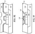
- FIGS. 6A-6Fillustrate another exemplary method to form a fuse structure in accordance with embodiments. These figures illustrate a cross-section of a cathode of the fuse structure, for example, the cathode 12 in FIG. 1 along line A-A.
- a first dielectric layer 202is provided, such as silicon dioxide, silicon nitride, silicon oxynitride, or the like.
- the first dielectric layer 202may be formed above a semiconductor substrate, such as part of an interlayer dielectric (ILD) or intermetal dielectric (IMD) layer in a semiconductor chip.
- a photoresist 204is patterned over the first dielectric layer 202 with opening 206 therein.
- the opening 206is patterned similar to the top surface illustrated in FIGS. 1 through 4 .
- the vertical dashed lines in the photoresist 204indicate the width of a fuse link in the subsequent fuse structure, and the horizontal dashed lines show the top surface of the photoresist 204 around other areas of opening 206 .
- the first dielectric layer 202is etched such that opening 206 is imposed into the dielectric layer 202 .
- a metal or polysilicon layer 208is formed over the first dielectric layer 202 , such as by a blanket deposition. If metal is used, the metal layer 208 may comprise copper or the like. Any excess metal or polysilicon is then removed, such as by a chemical mechanical polish (CMP).
- CMPchemical mechanical polish
- a metalsuch as titanium, cobalt, nickel, platinum, or the like, may be deposited over the polysilicon and annealed to form a silicide, such as titanium silicide, cobalt silicide, nickel silicide, platinum silicide, or other similar silicides.
- a second dielectric layer 210is deposited over the first dielectric layer 202 and the metal or polysilicon 208 .
- the second dielectric layer 210may be a subsequent ILD or IMD layer.
- a photoresist 212is deposited over the second dielectric layer 210 and patterned to expose portions of the dielectric layer 210 over the remaining metal or polysilicon layer 208 through openings 214 .
- an etch processis carried out to impose the pattern of openings 214 into the second dielectric layer 210 to form openings 218 .
- Another photoresist 216is then formed over the second dielectric layer 210 with an opening 220 patterned therein.
- An isotropic etchis then carried out to extend opening 220 into the second dielectric layer 210 so that contacts subsequently formed in openings 218 are coupled together.
- a conformal diffusion barrier layer 222is deposited over the structure and a metal 224 is deposited over the diffusion barrier layer 222 .
- the diffusion barrier layer 222may be any known barrier layer, such as titanium nitride, tantalum nitride, or the like.
- the metal 224may be copper, tungsten, or the like.
- vias 226are formed coupled to the metal or polysilicon layer 206 that is the cathode, and line 228 couples the vias 226 together and forms an area to which vias in subsequent IMD layers may be coupled. It is noted that line 228 is not depicted in FIG. 1 .
- the vias 226 thus formedhave a larger contact area and are not aligned with any fuse link, as indicated by the dashed lines. This process may result in the layout of the fuse structure 10 illustrated in FIG. 1 , but a person having ordinary skill in the art will readily understand any needed modifications to this process to form other embodiments, such as those in FIGS. 2 through 4 .
Landscapes
- Physics & Mathematics (AREA)
- Condensed Matter Physics & Semiconductors (AREA)
- General Physics & Mathematics (AREA)
- Engineering & Computer Science (AREA)
- Computer Hardware Design (AREA)
- Microelectronics & Electronic Packaging (AREA)
- Power Engineering (AREA)
- Design And Manufacture Of Integrated Circuits (AREA)
Abstract
Description
Claims (20)
Priority Applications (1)
| Application Number | Priority Date | Filing Date | Title |
|---|---|---|---|
| US15/863,169US11309244B2 (en) | 2009-10-30 | 2018-01-05 | Electrical fuse structure and method of formation |
Applications Claiming Priority (5)
| Application Number | Priority Date | Filing Date | Title |
|---|---|---|---|
| US25679209P | 2009-10-30 | 2009-10-30 | |
| US30858810P | 2010-02-26 | 2010-02-26 | |
| US12/771,768US8686536B2 (en) | 2009-10-30 | 2010-04-30 | Electrical fuse structure and method of formation |
| US14/231,231US9865536B2 (en) | 2009-10-30 | 2014-03-31 | Electrical fuse structure and method of formation |
| US15/863,169US11309244B2 (en) | 2009-10-30 | 2018-01-05 | Electrical fuse structure and method of formation |
Related Parent Applications (1)
| Application Number | Title | Priority Date | Filing Date |
|---|---|---|---|
| US14/231,231ContinuationUS9865536B2 (en) | 2009-10-30 | 2014-03-31 | Electrical fuse structure and method of formation |
Publications (2)
| Publication Number | Publication Date |
|---|---|
| US20180130741A1 US20180130741A1 (en) | 2018-05-10 |
| US11309244B2true US11309244B2 (en) | 2022-04-19 |
Family
ID=43836546
Family Applications (1)
| Application Number | Title | Priority Date | Filing Date |
|---|---|---|---|
| US15/863,169Active2030-10-01US11309244B2 (en) | 2009-10-30 | 2018-01-05 | Electrical fuse structure and method of formation |
Country Status (2)
| Country | Link |
|---|---|
| US (1) | US11309244B2 (en) |
| DE (1) | DE102010045073B4 (en) |
Families Citing this family (1)
| Publication number | Priority date | Publication date | Assignee | Title |
|---|---|---|---|---|
| US10770393B2 (en)* | 2018-03-20 | 2020-09-08 | International Business Machines Corporation | BEOL thin film resistor |
Citations (44)
| Publication number | Priority date | Publication date | Assignee | Title |
|---|---|---|---|---|
| US5212102A (en) | 1990-08-22 | 1993-05-18 | National Semiconductor Corporation | Method of making polysilicon Schottky clamped transistor and vertical fuse devices |
| US5244836A (en) | 1991-12-30 | 1993-09-14 | North American Philips Corporation | Method of manufacturing fusible links in semiconductor devices |
| US5427979A (en) | 1993-10-18 | 1995-06-27 | Vlsi Technology, Inc. | Method for making multi-level antifuse structure |
| US5472901A (en) | 1994-12-02 | 1995-12-05 | Lsi Logic Corporation | Process for formation of vias (or contact openings) and fuses in the same insulation layer with minimal additional steps |
| US5538924A (en) | 1995-09-05 | 1996-07-23 | Vanguard International Semiconductor Co. | Method of forming a moisture guard ring for integrated circuit applications |
| US5573970A (en) | 1994-07-14 | 1996-11-12 | Vlsi Technology, Inc. | Method for reducing contamination of anti-fuse material in an anti-fuse structure |
| US5618750A (en) | 1995-04-13 | 1997-04-08 | Texas Instruments Incorporated | Method of making fuse with non-corrosive termination of corrosive fuse material |
| US5702982A (en) | 1996-03-28 | 1997-12-30 | Taiwan Semiconductor Manufacturing Company, Ltd. | Method for making metal contacts and interconnections concurrently on semiconductor integrated circuits |
| US5854510A (en) | 1996-12-27 | 1998-12-29 | Vlsi Technology, Inc. | Low power programmable fuse structures |
| US5879982A (en) | 1996-12-17 | 1999-03-09 | Samsung Electronics Co., Ltd. | Methods of forming integrated circuit memory devices having improved electrical interconnects therein |
| US5907788A (en) | 1994-07-29 | 1999-05-25 | Nec Corporation | Semiconductor device capable of easily filling contact conductor plug in contact hole |
| US5953635A (en) | 1996-12-19 | 1999-09-14 | Intel Corporation | Interlayer dielectric with a composite dielectric stack |
| US5970346A (en) | 1997-09-19 | 1999-10-19 | Taiwan Semiconductor Manufacturing Company, Ltd. | Fuse window guard ring structure for nitride capped self aligned contact processes |
| US5989784A (en) | 1998-04-06 | 1999-11-23 | Taiwan Semiconductor Manufacturing Company, Ltd. | Etch recipe for embedded DRAM passivation with etch stopping layer scheme |
| US6027999A (en) | 1998-09-10 | 2000-02-22 | Chartered Semiconductor Manufacturing, Ltd. | Pad definition to achieve highly reflective plate without affecting bondability |
| US6078088A (en) | 1999-01-05 | 2000-06-20 | Advanced Micro Devices, Inc. | Low dielectric semiconductor device with rigid lined interconnection system |
| US6162686A (en) | 1998-09-18 | 2000-12-19 | Taiwan Semiconductor Manufacturing Company | Method for forming a fuse in integrated circuit application |
| CN1277448A (en) | 1999-04-14 | 2000-12-20 | 国际商业机器公司 | Slotted contact for making required voltage of electrofusion fuse minimum |
| US6242790B1 (en) | 1999-08-30 | 2001-06-05 | Advanced Micro Devices, Inc. | Using polysilicon fuse for IC programming |
| US6277674B1 (en) | 1998-10-02 | 2001-08-21 | Micron Technology, Inc. | Semiconductor fuses, methods of using the same, methods of making the same, and semiconductor devices containing the same |
| US6433404B1 (en) | 2000-02-07 | 2002-08-13 | Infineon Technologies Ag | Electrical fuses for semiconductor devices |
| US6436738B1 (en) | 2001-08-22 | 2002-08-20 | Taiwan Semiconductor Manufacturing Company | Silicide agglomeration poly fuse device |
| US20030054629A1 (en)* | 2001-09-18 | 2003-03-20 | Mitsubishi Denki Kabushiki Kaisha | Semiconductor device and manufacturing method thereof |
| US6642601B2 (en) | 2000-12-18 | 2003-11-04 | Texas Instruments Incorporated | Low current substantially silicide fuse for integrated circuits |
| US6661330B1 (en) | 2002-07-23 | 2003-12-09 | Texas Instruments Incorporated | Electrical fuse for semiconductor integrated circuits |
| US6670824B2 (en) | 2002-03-20 | 2003-12-30 | Agilent Technologies, Inc. | Integrated polysilicon fuse and diode |
| US20040121584A1 (en)* | 2002-12-16 | 2004-06-24 | Lee Ja Suk | Method of manufacturing a semiconductor device |
| US20050189613A1 (en) | 2004-02-27 | 2005-09-01 | Nobuaki Otsuka | Semiconductor device as electrically programmable fuse element and method of programming the same |
| US20050285222A1 (en) | 2004-06-29 | 2005-12-29 | Kong-Beng Thei | New fuse structure |
| US20050285224A1 (en) | 2004-06-29 | 2005-12-29 | Matsushita Electric Industrial Co., Ltd. | Semiconductor device and manufacturing method thereof |
| US7109564B2 (en) | 2004-03-22 | 2006-09-19 | Taiwan Semiconductor Manufacturing Company, Ltd. | Low power fuse structure and method of making the same |
| US20070210413A1 (en) | 2006-03-09 | 2007-09-13 | International Business Machines Corporation | Electrically programmable fuse structures with narrowed width regions configured to enhance current crowding and methods of fabrication thereof |
| US20070298526A1 (en) | 2003-04-11 | 2007-12-27 | Berry Wayne S | Programmable semiconductor device |
| US20080029843A1 (en) | 2006-05-11 | 2008-02-07 | International Business Machines Corporation | E-Fuse and Method for Fabricating E-Fuses Integrating Polysilicon Resistor Masks |
| US20080186788A1 (en) | 2007-02-02 | 2008-08-07 | Infineon Technologies Ag | Electrical fuse and associated methods |
| US20080211059A1 (en) | 2007-01-17 | 2008-09-04 | Samsung Electronics Co., Ltd. | Electronic fuse having heat spreading structure |
| US20090021338A1 (en) | 2007-07-18 | 2009-01-22 | International Business Machines Corporation | Electrical fuse having a cavity thereupon |
| US20090231020A1 (en) | 2008-03-06 | 2009-09-17 | Nec Electronics Corporation | Electrical fuse, semiconductor device and method of disconnecting electrical fuse |
| US20090243032A1 (en) | 2008-03-27 | 2009-10-01 | Shi-Bai Chen | Electrical fuse structure |
| US20090261450A1 (en) | 2008-04-21 | 2009-10-22 | Hsin-Li Cheng | Electrical Fuse Structure and Method |
| US20090283853A1 (en)* | 2008-05-13 | 2009-11-19 | Frank Huebinger | Programmable Devices and Methods of Manufacture Thereof |
| US8686536B2 (en) | 2009-10-30 | 2014-04-01 | Taiwan Semiconductor Manufacturing Company, Ltd. | Electrical fuse structure and method of formation |
| US20140203369A1 (en) | 2013-01-22 | 2014-07-24 | Semiconductor Manufacturing International Corp. | Fin field-effect transistors and fabrication method thereof |
| US20140319651A1 (en) | 2009-10-30 | 2014-10-30 | Taiwan Semiconductor Manufacturing Company, Ltd. | Electrical Fuse Structure and Method of Formation |
Family Cites Families (1)
| Publication number | Priority date | Publication date | Assignee | Title |
|---|---|---|---|---|
| KR100838805B1 (en)* | 2003-07-14 | 2008-06-17 | 가부시키가이샤후지쿠라 | Electrolyte composition, photoelectric conversion element and dye-sensitized solar cell using same |
- 2010
- 2010-09-10DEDE102010045073.1Apatent/DE102010045073B4/enactiveActive
- 2018
- 2018-01-05USUS15/863,169patent/US11309244B2/enactiveActive
Patent Citations (52)
| Publication number | Priority date | Publication date | Assignee | Title |
|---|---|---|---|---|
| US5212102A (en) | 1990-08-22 | 1993-05-18 | National Semiconductor Corporation | Method of making polysilicon Schottky clamped transistor and vertical fuse devices |
| US5244836A (en) | 1991-12-30 | 1993-09-14 | North American Philips Corporation | Method of manufacturing fusible links in semiconductor devices |
| US5427979A (en) | 1993-10-18 | 1995-06-27 | Vlsi Technology, Inc. | Method for making multi-level antifuse structure |
| US5573970A (en) | 1994-07-14 | 1996-11-12 | Vlsi Technology, Inc. | Method for reducing contamination of anti-fuse material in an anti-fuse structure |
| US5907788A (en) | 1994-07-29 | 1999-05-25 | Nec Corporation | Semiconductor device capable of easily filling contact conductor plug in contact hole |
| US5472901A (en) | 1994-12-02 | 1995-12-05 | Lsi Logic Corporation | Process for formation of vias (or contact openings) and fuses in the same insulation layer with minimal additional steps |
| US5618750A (en) | 1995-04-13 | 1997-04-08 | Texas Instruments Incorporated | Method of making fuse with non-corrosive termination of corrosive fuse material |
| US5538924A (en) | 1995-09-05 | 1996-07-23 | Vanguard International Semiconductor Co. | Method of forming a moisture guard ring for integrated circuit applications |
| US5702982A (en) | 1996-03-28 | 1997-12-30 | Taiwan Semiconductor Manufacturing Company, Ltd. | Method for making metal contacts and interconnections concurrently on semiconductor integrated circuits |
| US5879982A (en) | 1996-12-17 | 1999-03-09 | Samsung Electronics Co., Ltd. | Methods of forming integrated circuit memory devices having improved electrical interconnects therein |
| US5953635A (en) | 1996-12-19 | 1999-09-14 | Intel Corporation | Interlayer dielectric with a composite dielectric stack |
| US5882998A (en) | 1996-12-27 | 1999-03-16 | Vlsi Technology, Inc. | Low power programmable fuse structures and methods for making the same |
| US5854510A (en) | 1996-12-27 | 1998-12-29 | Vlsi Technology, Inc. | Low power programmable fuse structures |
| US5970346A (en) | 1997-09-19 | 1999-10-19 | Taiwan Semiconductor Manufacturing Company, Ltd. | Fuse window guard ring structure for nitride capped self aligned contact processes |
| US5989784A (en) | 1998-04-06 | 1999-11-23 | Taiwan Semiconductor Manufacturing Company, Ltd. | Etch recipe for embedded DRAM passivation with etch stopping layer scheme |
| US6027999A (en) | 1998-09-10 | 2000-02-22 | Chartered Semiconductor Manufacturing, Ltd. | Pad definition to achieve highly reflective plate without affecting bondability |
| US6162686A (en) | 1998-09-18 | 2000-12-19 | Taiwan Semiconductor Manufacturing Company | Method for forming a fuse in integrated circuit application |
| US6277674B1 (en) | 1998-10-02 | 2001-08-21 | Micron Technology, Inc. | Semiconductor fuses, methods of using the same, methods of making the same, and semiconductor devices containing the same |
| US6078088A (en) | 1999-01-05 | 2000-06-20 | Advanced Micro Devices, Inc. | Low dielectric semiconductor device with rigid lined interconnection system |
| CN1277448A (en) | 1999-04-14 | 2000-12-20 | 国际商业机器公司 | Slotted contact for making required voltage of electrofusion fuse minimum |
| US6242790B1 (en) | 1999-08-30 | 2001-06-05 | Advanced Micro Devices, Inc. | Using polysilicon fuse for IC programming |
| US6433404B1 (en) | 2000-02-07 | 2002-08-13 | Infineon Technologies Ag | Electrical fuses for semiconductor devices |
| US6642601B2 (en) | 2000-12-18 | 2003-11-04 | Texas Instruments Incorporated | Low current substantially silicide fuse for integrated circuits |
| US6436738B1 (en) | 2001-08-22 | 2002-08-20 | Taiwan Semiconductor Manufacturing Company | Silicide agglomeration poly fuse device |
| US20030054629A1 (en)* | 2001-09-18 | 2003-03-20 | Mitsubishi Denki Kabushiki Kaisha | Semiconductor device and manufacturing method thereof |
| US6670824B2 (en) | 2002-03-20 | 2003-12-30 | Agilent Technologies, Inc. | Integrated polysilicon fuse and diode |
| US6661330B1 (en) | 2002-07-23 | 2003-12-09 | Texas Instruments Incorporated | Electrical fuse for semiconductor integrated circuits |
| US20040121584A1 (en)* | 2002-12-16 | 2004-06-24 | Lee Ja Suk | Method of manufacturing a semiconductor device |
| US20070298526A1 (en) | 2003-04-11 | 2007-12-27 | Berry Wayne S | Programmable semiconductor device |
| US20050189613A1 (en) | 2004-02-27 | 2005-09-01 | Nobuaki Otsuka | Semiconductor device as electrically programmable fuse element and method of programming the same |
| US7109564B2 (en) | 2004-03-22 | 2006-09-19 | Taiwan Semiconductor Manufacturing Company, Ltd. | Low power fuse structure and method of making the same |
| US20050285222A1 (en) | 2004-06-29 | 2005-12-29 | Kong-Beng Thei | New fuse structure |
| US20050285224A1 (en) | 2004-06-29 | 2005-12-29 | Matsushita Electric Industrial Co., Ltd. | Semiconductor device and manufacturing method thereof |
| JP2006013338A (en) | 2004-06-29 | 2006-01-12 | Matsushita Electric Ind Co Ltd | Semiconductor device and manufacturing method thereof |
| US20070210413A1 (en) | 2006-03-09 | 2007-09-13 | International Business Machines Corporation | Electrically programmable fuse structures with narrowed width regions configured to enhance current crowding and methods of fabrication thereof |
| US20080029843A1 (en) | 2006-05-11 | 2008-02-07 | International Business Machines Corporation | E-Fuse and Method for Fabricating E-Fuses Integrating Polysilicon Resistor Masks |
| US20080211059A1 (en) | 2007-01-17 | 2008-09-04 | Samsung Electronics Co., Ltd. | Electronic fuse having heat spreading structure |
| US20080186788A1 (en) | 2007-02-02 | 2008-08-07 | Infineon Technologies Ag | Electrical fuse and associated methods |
| US20090021338A1 (en) | 2007-07-18 | 2009-01-22 | International Business Machines Corporation | Electrical fuse having a cavity thereupon |
| US20090231020A1 (en) | 2008-03-06 | 2009-09-17 | Nec Electronics Corporation | Electrical fuse, semiconductor device and method of disconnecting electrical fuse |
| US20090243032A1 (en) | 2008-03-27 | 2009-10-01 | Shi-Bai Chen | Electrical fuse structure |
| US20090261450A1 (en) | 2008-04-21 | 2009-10-22 | Hsin-Li Cheng | Electrical Fuse Structure and Method |
| CN101567360A (en) | 2008-04-21 | 2009-10-28 | 台湾积体电路制造股份有限公司 | Electrical fuse structure and method |
| US7642176B2 (en) | 2008-04-21 | 2010-01-05 | Taiwan Semiconductor Manufacturing Company, Ltd. | Electrical fuse structure and method |
| US20100090751A1 (en) | 2008-04-21 | 2010-04-15 | Hsin-Li Cheng | Electrical Fuse Structure and Method |
| US20090283853A1 (en)* | 2008-05-13 | 2009-11-19 | Frank Huebinger | Programmable Devices and Methods of Manufacture Thereof |
| US8686536B2 (en) | 2009-10-30 | 2014-04-01 | Taiwan Semiconductor Manufacturing Company, Ltd. | Electrical fuse structure and method of formation |
| US20140319651A1 (en) | 2009-10-30 | 2014-10-30 | Taiwan Semiconductor Manufacturing Company, Ltd. | Electrical Fuse Structure and Method of Formation |
| US9741658B2 (en) | 2009-10-30 | 2017-08-22 | Taiwan Semiconductor Manufacturing Company, Ltd. | Electrical fuse structure and method of formation |
| US20170345758A1 (en) | 2009-10-30 | 2017-11-30 | Taiwan Semiconductor Manufacturing Company, Ltd. | Electrical Fuse Structure and Method of Formation |
| US9865536B2 (en) | 2009-10-30 | 2018-01-09 | Taiwan Semiconductor Manufacturing Company, Ltd. | Electrical fuse structure and method of formation |
| US20140203369A1 (en) | 2013-01-22 | 2014-07-24 | Semiconductor Manufacturing International Corp. | Fin field-effect transistors and fabrication method thereof |
Non-Patent Citations (1)
| Title |
|---|
| German Patent and Trademark Office, German Patent Office Action dated Oct. 17, 2016, for Application No. 10 2010 045 073.1, 6 pages. |
Also Published As
| Publication number | Publication date |
|---|---|
| US20180130741A1 (en) | 2018-05-10 |
| DE102010045073B4 (en) | 2021-04-22 |
| DE102010045073A1 (en) | 2011-05-05 |
Similar Documents
| Publication | Publication Date | Title |
|---|---|---|
| US8686536B2 (en) | Electrical fuse structure and method of formation | |
| US12033939B2 (en) | Electrical fuse structure and method of formation | |
| US10249496B2 (en) | Narrowed feature formation during a double patterning process | |
| US7378718B2 (en) | Fuse element with adjustable resistance | |
| US7786520B2 (en) | Embedded semiconductor device including planarization resistance patterns and method of manufacturing the same | |
| US8237457B2 (en) | Replacement-gate-compatible programmable electrical antifuse | |
| US20070246796A1 (en) | Semiconductor device with improved contact fuse | |
| US10811353B2 (en) | Sub-ground rule e-Fuse structure | |
| US10515894B2 (en) | Enhanced self-alignment of vias for a semiconductor device | |
| US7651893B2 (en) | Metal electrical fuse structure | |
| US11348870B2 (en) | Electrical fuse formation during a multiple patterning process | |
| US7768128B2 (en) | Semiconductor memory devices including a damascene wiring line | |
| US11309244B2 (en) | Electrical fuse structure and method of formation | |
| CN107622991B (en) | Electric fuse structure and method of making the same | |
| KR101159996B1 (en) | Electrical fuse structure and method of formation | |
| US20250218935A1 (en) | Bimetallic fuse element between metal levels | |
| US20250096123A1 (en) | Tapered antifuse | |
| US20250096122A1 (en) | Vertical antifuse | |
| TWI666756B (en) | An electrical fuse and making method thereof | |
| CN102034790A (en) | Electric fuse structure and manufacturing method thereof |
Legal Events
| Date | Code | Title | Description |
|---|---|---|---|
| AS | Assignment | Owner name:TAIWAN SEMICONDUCTOR MANUFACTURING CO., LTD., TAIWAN Free format text:ASSIGNMENT OF ASSIGNORS INTEREST;ASSIGNORS:WU, SHIEN-YANG;KUNG, WEI-CHANG;REEL/FRAME:044545/0812 Effective date:20140305 Owner name:TAIWAN SEMICONDUCTOR MANUFACTURING CO., LTD., TAIW Free format text:ASSIGNMENT OF ASSIGNORS INTEREST;ASSIGNORS:WU, SHIEN-YANG;KUNG, WEI-CHANG;REEL/FRAME:044545/0812 Effective date:20140305 | |
| FEPP | Fee payment procedure | Free format text:ENTITY STATUS SET TO UNDISCOUNTED (ORIGINAL EVENT CODE: BIG.); ENTITY STATUS OF PATENT OWNER: LARGE ENTITY | |
| STPP | Information on status: patent application and granting procedure in general | Free format text:DOCKETED NEW CASE - READY FOR EXAMINATION | |
| STPP | Information on status: patent application and granting procedure in general | Free format text:NON FINAL ACTION MAILED | |
| STPP | Information on status: patent application and granting procedure in general | Free format text:RESPONSE TO NON-FINAL OFFICE ACTION ENTERED AND FORWARDED TO EXAMINER | |
| STPP | Information on status: patent application and granting procedure in general | Free format text:NON FINAL ACTION MAILED | |
| STPP | Information on status: patent application and granting procedure in general | Free format text:RESPONSE AFTER FINAL ACTION FORWARDED TO EXAMINER | |
| STPP | Information on status: patent application and granting procedure in general | Free format text:DOCKETED NEW CASE - READY FOR EXAMINATION | |
| STPP | Information on status: patent application and granting procedure in general | Free format text:NON FINAL ACTION MAILED | |
| STPP | Information on status: patent application and granting procedure in general | Free format text:RESPONSE TO NON-FINAL OFFICE ACTION ENTERED AND FORWARDED TO EXAMINER | |
| STPP | Information on status: patent application and granting procedure in general | Free format text:NOTICE OF ALLOWANCE MAILED -- APPLICATION RECEIVED IN OFFICE OF PUBLICATIONS | |
| STPP | Information on status: patent application and granting procedure in general | Free format text:PUBLICATIONS -- ISSUE FEE PAYMENT VERIFIED | |
| STCF | Information on status: patent grant | Free format text:PATENTED CASE | |
| MAFP | Maintenance fee payment | Free format text:PAYMENT OF MAINTENANCE FEE, 4TH YEAR, LARGE ENTITY (ORIGINAL EVENT CODE: M1551); ENTITY STATUS OF PATENT OWNER: LARGE ENTITY Year of fee payment:4 |