US11301151B2 - Multi-die memory apparatus and identification method thereof - Google Patents
Multi-die memory apparatus and identification method thereofDownload PDFInfo
- Publication number
- US11301151B2 US11301151B2US16/870,848US202016870848AUS11301151B2US 11301151 B2US11301151 B2US 11301151B2US 202016870848 AUS202016870848 AUS 202016870848AUS 11301151 B2US11301151 B2US 11301151B2
- Authority
- US
- United States
- Prior art keywords
- memory devices
- identification
- time
- memory device
- identified
- Prior art date
- Legal status (The legal status is an assumption and is not a legal conclusion. Google has not performed a legal analysis and makes no representation as to the accuracy of the status listed.)
- Active
Links
Images


Classifications
- G—PHYSICS
- G06—COMPUTING OR CALCULATING; COUNTING
- G06F—ELECTRIC DIGITAL DATA PROCESSING
- G06F3/00—Input arrangements for transferring data to be processed into a form capable of being handled by the computer; Output arrangements for transferring data from processing unit to output unit, e.g. interface arrangements
- G06F3/06—Digital input from, or digital output to, record carriers, e.g. RAID, emulated record carriers or networked record carriers
- G06F3/0601—Interfaces specially adapted for storage systems
- G06F3/0668—Interfaces specially adapted for storage systems adopting a particular infrastructure
- G06F3/0671—In-line storage system
- G06F3/0683—Plurality of storage devices
- G06F3/0688—Non-volatile semiconductor memory arrays
- G—PHYSICS
- G06—COMPUTING OR CALCULATING; COUNTING
- G06F—ELECTRIC DIGITAL DATA PROCESSING
- G06F3/00—Input arrangements for transferring data to be processed into a form capable of being handled by the computer; Output arrangements for transferring data from processing unit to output unit, e.g. interface arrangements
- G06F3/06—Digital input from, or digital output to, record carriers, e.g. RAID, emulated record carriers or networked record carriers
- G06F3/0601—Interfaces specially adapted for storage systems
- G06F3/0628—Interfaces specially adapted for storage systems making use of a particular technique
- G06F3/0629—Configuration or reconfiguration of storage systems
- G06F3/0632—Configuration or reconfiguration of storage systems by initialisation or re-initialisation of storage systems
- G—PHYSICS
- G06—COMPUTING OR CALCULATING; COUNTING
- G06F—ELECTRIC DIGITAL DATA PROCESSING
- G06F3/00—Input arrangements for transferring data to be processed into a form capable of being handled by the computer; Output arrangements for transferring data from processing unit to output unit, e.g. interface arrangements
- G06F3/06—Digital input from, or digital output to, record carriers, e.g. RAID, emulated record carriers or networked record carriers
- G06F3/0601—Interfaces specially adapted for storage systems
- G06F3/0602—Interfaces specially adapted for storage systems specifically adapted to achieve a particular effect
- G06F3/0604—Improving or facilitating administration, e.g. storage management
- G—PHYSICS
- G06—COMPUTING OR CALCULATING; COUNTING
- G06F—ELECTRIC DIGITAL DATA PROCESSING
- G06F3/00—Input arrangements for transferring data to be processed into a form capable of being handled by the computer; Output arrangements for transferring data from processing unit to output unit, e.g. interface arrangements
- G06F3/06—Digital input from, or digital output to, record carriers, e.g. RAID, emulated record carriers or networked record carriers
- G06F3/0601—Interfaces specially adapted for storage systems
- G06F3/0628—Interfaces specially adapted for storage systems making use of a particular technique
- G06F3/0655—Vertical data movement, i.e. input-output transfer; data movement between one or more hosts and one or more storage devices
- G06F3/0658—Controller construction arrangements
- G—PHYSICS
- G06—COMPUTING OR CALCULATING; COUNTING
- G06F—ELECTRIC DIGITAL DATA PROCESSING
- G06F3/00—Input arrangements for transferring data to be processed into a form capable of being handled by the computer; Output arrangements for transferring data from processing unit to output unit, e.g. interface arrangements
- G06F3/06—Digital input from, or digital output to, record carriers, e.g. RAID, emulated record carriers or networked record carriers
- G06F3/0601—Interfaces specially adapted for storage systems
- G06F3/0668—Interfaces specially adapted for storage systems adopting a particular infrastructure
- G06F3/0671—In-line storage system
- G06F3/0673—Single storage device
- H—ELECTRICITY
- H01—ELECTRIC ELEMENTS
- H01L—SEMICONDUCTOR DEVICES NOT COVERED BY CLASS H10
- H01L25/00—Assemblies consisting of a plurality of semiconductor or other solid state devices
- H01L25/03—Assemblies consisting of a plurality of semiconductor or other solid state devices all the devices being of a type provided for in a single subclass of subclasses H10B, H10D, H10F, H10H, H10K or H10N, e.g. assemblies of rectifier diodes
- H01L25/04—Assemblies consisting of a plurality of semiconductor or other solid state devices all the devices being of a type provided for in a single subclass of subclasses H10B, H10D, H10F, H10H, H10K or H10N, e.g. assemblies of rectifier diodes the devices not having separate containers
- H01L25/065—Assemblies consisting of a plurality of semiconductor or other solid state devices all the devices being of a type provided for in a single subclass of subclasses H10B, H10D, H10F, H10H, H10K or H10N, e.g. assemblies of rectifier diodes the devices not having separate containers the devices being of a type provided for in group H10D89/00
- H01L25/0657—Stacked arrangements of devices
- H—ELECTRICITY
- H01—ELECTRIC ELEMENTS
- H01L—SEMICONDUCTOR DEVICES NOT COVERED BY CLASS H10
- H01L25/00—Assemblies consisting of a plurality of semiconductor or other solid state devices
- H01L25/18—Assemblies consisting of a plurality of semiconductor or other solid state devices the devices being of the types provided for in two or more different main groups of the same subclass of H10B, H10D, H10F, H10H, H10K or H10N
- H—ELECTRICITY
- H01—ELECTRIC ELEMENTS
- H01L—SEMICONDUCTOR DEVICES NOT COVERED BY CLASS H10
- H01L2225/00—Details relating to assemblies covered by the group H01L25/00 but not provided for in its subgroups
- H01L2225/03—All the devices being of a type provided for in the same main group of the same subclass of class H10, e.g. assemblies of rectifier diodes
- H01L2225/04—All the devices being of a type provided for in the same main group of the same subclass of class H10, e.g. assemblies of rectifier diodes the devices not having separate containers
- H01L2225/065—All the devices being of a type provided for in the same main group of the same subclass of class H10
- H01L2225/06503—Stacked arrangements of devices
- H01L2225/06541—Conductive via connections through the device, e.g. vertical interconnects, through silicon via [TSV]
Definitions
- the present inventiongenerally relates to a multi-die memory apparatus and an identification method thereof, in particular, to the multi-die memory apparatus for performing the identification method without boding difference.
- Multi-die package or stacked-die package apparatusesthat encloses a number of integrated circuits (IC) in a chip carrier package has been widely used to maximize the capacities and performance as well as the area.
- ICintegrated circuits
- a controllercould specify a memory device that it wants to access.
- the present inventionprovides a memory apparatus and an identification method thereof which can identification individual memory device without using bonding difference.
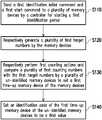
- the identification methodincludes: sending a identification initial command and a first start command to a plurality of memory devices by a controller for starting a first identification period; respectively generating a plurality of first target numbers by the memory devices; respectively performing first counting actions and comparing a plurality of first counting numbers with the first target numbers by a plurality of un-identified memory devices to set a first time-up memory device of the memory devices; and, setting an identification code of the first time-up memory device of the un-identified memory devices to be a first value.
- the memory apparatusincludes a controller and a plurality of memory devices.
- the memory devicesare coupled to the controller.
- the memory apparatusperforms the identification method mentioned above to identify each of the memory devices for accessing.
- the memory devices in the multi-die memory apparatusgenerate a plurality of target numbers.
- the memory devicesperform counting operation and compare counting numbers with the target numbers to determine the first time-up memory device. That is, the identification code of the first time-up memory device can be set accordingly, and no special bonding structure is necessary for the memory devices.
- FIG. 1is a flow chart of an identification method for a multi-die memory apparatus according to an embodiment of present disclosure.
- FIG. 2is a waveform plot of the identification method of a multi-die memory apparatus according to an embodiment of present disclosure.
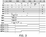
- FIG. 3is a waveform plot of the identification method of a multi-die memory apparatus according to another embodiment of present disclosure.
- FIG. 4is a schematic diagram of a multi-die memory apparatus according to an embodiment of present disclosure.
- FIG. 5is a block diagram of a memory device of a multi-die memory apparatus according to an embodiment of present disclosure.
- FIG. 6is a block diagram of a controller of a multi-die memory apparatus according to an embodiment of present disclosure.
- the multi-die memory apparatusincludes a controller and a plurality of memory devices.
- the controlleris coupled to the memory devices.
- the memory devicesmay be arranged by a stack structure, and may be connected to each other by through-silicon-vias (TSVs).
- TSVsthrough-silicon-vias
- Each of the memory devicesmay be one die, and may be a flash memory die.
- the controllersends a identification initial command and a first start command to the memory devices for starting a first identification period.
- the identification initial commandis used to enable an identification operation
- the first start commandis used to start a first identification period of the identification operation.
- each of the memory devicescan has one number sequence generator, and the number sequence generator can generate one of the first target numbers when the corresponding memory device receives the first start command.
- the first target numbers generating by the memory devicesmay be different or some of the first target numbers may be the same.
- the number sequence generatormay be a random number generator.
- the memory devicesmay respectively perform counting actions to generate a plurality of first counting numbers.
- the memory devicesalso respectively compare the first target numbers with the first counting numbers to step a first time-up memory device of the memory devices in the step S 130 .
- all of the memory devicesare un-identified memory devices.
- the memory devicesreceive the first start command, the memory devices respectively generate the first target numbers, and perform counting actions according to the first start command.
- Each of the memory devicescompares the corresponding first target number with the corresponding first counting number.
- the first counting numberequals to the first target number, the corresponding memory device is the first time-up memory device can be determined.
- the first identification periodcan be end by the controller, and the counting actions of all of the memory devices are terminated.
- the memory device Amay inform the controller by a time-up signal, and the controller can end the first identification period according to the time-up signal, and stops the counting actions of all of the memory devices.
- an identification code of the first time-up memory devicecan be set to a first value, and the first time-up memory device is turned to an identified memory device.
- identification codes of all the memory devicesare 0.
- the identification code of the first memory deviceremains in 0, and the identification codes of others memory device are increased by 1.
- the identification code of the first memory devicecan be set to 0 (the first value).
- the steps S 120 to S 140can be executed repeatedly for several times.
- a second identification period of the identification operationcan be started by a second start command from the controller.
- the un-identified memory devicescan generate a plurality of second target numbers.
- the un-identified memory devicescan perform second counting actions and compare second counting numbers with the second target numbers respectively to determine a second time-up memory device. After the second time-up memory device is determined, the second counting actions can be terminated by the controller, and the identification code of the second time-up memory device can be set.
- FIG. 2is a waveform plot of the identification method of a multi-die memory apparatus according to an embodiment of present disclosure.
- a controller of the multi-die memory apparatuscan send an identification initial command IIC by a signal port C 1 to a plurality of memory devices.
- the controllersends the first start command TSC 1 , and counting actions of all of the memory devices are started at a time point tP 1 according to the first start command TSC 1 .
- the signal port C 1may be used to transmit identification commands for the identification method of present embodiment.
- the signal port C 1may be used to transmit data and/or commands for normal accessing operation (read operation and/or write operation) for the memory devices.
- the memory deviceswhen the memory devices receive the first start command TSC 1 , the memory devices respectively generate four first target numbers TD 1 ⁇ TD 4 . Since the first target number TD 2 is a minimum number of the four first target numbers TD 1 ⁇ TD 4 , the memory device corresponding to the first target number TD 2 can be a first time-up memory device. Accordingly, a time-up signal TUP 2 with an actual pulse P 1 can be generated. Besides, the first time-up memory device also pulls up the flag IDTFD 2 to a logic level 1 (a second logic level) at a time point tP 2 .
- all of the time-up signals TUP 1 ⁇ TUP 4may be tied together for generating a status signal S 1 .
- information of all the time-up signals TUP 1 ⁇ TUP 4can be transported to the controller by a signal wire.
- a low pulsecan be generated on the status signal S 1 .
- the controllercan end the first identification period, and stops all the counting actions of the memory devices.
- the counting actions of the memory devicescan be stopped by the memory devices themselves rather than the controller according to the status signal S 1 .
- the controllercan count a number of identified memory devices according to the status signal S 1 to generate an identified count IDC. In detail, if there is one low pulse found in the status S 1 , the controller may increase the identified count IDC by 1.
- the controllermay send a second start command TSC 2 to start a second identification period.
- the second identification periodall of un-identified memory devices start second counting actions according to the second start command TSC 2 .
- the un-identified memory devicesrespectively generate a plurality of second target numbers, and compare the second target numbers with a plurality of second counting numbers, respectively. Accordingly, a second time-up memory device can be determined, and another actual pulse P 2 can be generated on the time-up signal TUP 4 at a time point tP 3 , and a second low pulse can be generated on the status signal S 1 .
- the identified count IDCcan be increased to 2 by the controller.
- the identification codes ID 1 and ID 3increase to 2 correspondingly, and the identification code ID 4 keeps on 1. That is, the memory device corresponding to the identification code ID 4 is set to a second identified memory device.
- the controllercan send a third start command TSC 3 and a fourth start command TSC 3 in sequence.
- actual pulses P 3 and P 4can be respectively generated on the time-up signals TUP 3 and TUP 1 , and two low pulses can be generated on the status signal S 1 at time points tP 4 and tP 5 , respectively.
- the controllercan send an identification end command EIC to end this identification operation. After the identification operation has been completed, the identification codes ID 1 ⁇ ID 4 are respectively ser to 3, 0, 2 and 1. All of the memory devices are identified successfully.
- the identification codes ID 1 ⁇ ID 4can be respectively saved to the memory devices.
- the memory devicesmay be non-volatile memory devices, such as flash memory devices.
- the memory devicesmay be volatile memory devices, such as dynamic or static random accessing memory (DRAM or SRAM) devices.
- DRAM or SRAMdynamic or static random accessing memory
- the identification codes ID 1 ⁇ ID 4may be generated after each of power up sequences, and the identification codes ID 1 ⁇ ID 4 may be loss after power down. In some embodiments, the identification codes may be generated after each power up even if the memory device is non-volatile type.
- the flags IDTFD 1 ⁇ IDTFD 4are respectively set to logic level 1 at the time points tP 5 , tP 2 , tP 4 and tP 3 .
- the flags IDTFD 1 ⁇ IDTFD 4is set logic level 1, the corresponding memory device is the identified memory device.
- the status signal S 1may be transmit by part of data pins of each of the memory devices. Or the status signal S 1 may be transmit by any one specific pin in addition to data or control pin of each of the memory devices.
- FIG. 3is a waveform plot of the identification method of a multi-die memory apparatus according to another embodiment of present disclosure.
- the controllersets a delay time MTD, and calculates a waiting time for receiving pulse from any one of the time-up signals TUP 1 ⁇ TUP 4 . If the waiting time is larger than the delay time MTD, the controller can determine this identification operation is failed. Correspondingly, the controller can re-send the identification initial command IIC and the first start command TSC for re-starting a new identification operation and the first identification period.
- FIG. 4is a schematic diagram of a multi-die memory apparatus according to an embodiment of present disclosure.
- the multi-die memory apparatus 400includes a controller 410 and a plurality of memory devices 421 ⁇ 42 N.
- the controller 410is coupled to the memory devices 421 ⁇ 42 N, and can send one or more commands to the memory devices 421 ⁇ 42 N through a command port C 1 .
- the controller 410 and the memory devices 421 ⁇ 42 Nalso can transport data signals DATA and a synchronization signal DSYNC with each other.
- the memory devices 421 ⁇ 42 Ncan commonly send a status signal S 1 to the controller, where the status signal S 1 is generated by a plurality of time-up signals of the memory devices 421 ⁇ 42 N.
- the status signal S 1can be pulled up by a weak pull high circuit.
- the weak pull high circuitmay be a resistor or a transistor with a long length channel.
- the time-up signals from the memory devices 421 ⁇ 42 Ncan be respectively generated by a plurality of strong pull low circuit, such as a current sinker. That is, if one of the time-up signals is pulled to a low voltage level, the status signal S 1 can be pulled to the low voltage level accordingly, and if none of the time-up signals is pulled to the low voltage level, the status signal S 1 can be pulled on a high voltage level.
- the controllercan send an identification initial command and a plurality of start commands to enable an identification operation on the memory devices 421 ⁇ 42 N.
- the memory devices 421 ⁇ 42 Ncan respectively generate the time-up signals, and the status signal generated by the time-up signals can be sent back to the controller 410 .
- the controller 41can control a flow of the identification operation according to the status signal S 1 , and a plurality of identification codes of the memory devices 421 ⁇ 42 N can be set accordingly. Detail operations of the identification operation has been detailly described in above embodiments, and no more repeated description here.
- the memory devices 421 ⁇ 42 Nmay be connected to each other by a plurality of through-silicon-vias (TSVs), and the multi-die memory apparatus 400 can be implemented in the three-dimension (3D) integrated circuit (IC) packaging technology.
- TSVsthrough-silicon-vias
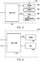
- FIG. 5is a block diagram of a memory device of a multi-die memory apparatus according to an embodiment of present disclosure.
- the memory device 500includes a logic circuit 510 , a timer 520 , a number sequence generator 530 and registers 540 and 550 .
- the number sequence generator 530is used to generate a target number TN according to a start command sent by a controller in the multi-die memory apparatus.
- the number sequence generator 530can be a random number generator, and can be implemented by a linear feedback shift registers (LSFR).
- the timer 520is coupled to the number sequence generator 530 and the logic circuit 510 .
- the timer 520can perform a counting action, and compare a counting number with the target number TN to generate a time-up signal TUP.
- the timer 520can be implemented by a digital counter and performs the counting operation based on a clock.
- the timer 520can be implemented by an analogy circuit without the clock signal, where the analogy circuit can decide a delay time according to the target number TN, and decide a time point for generating a pulse on the time-up signal TUP according to the delay time.
- the registers 540 and 550are coupled to the logic circuit 510 .
- the register 550is used to recode an identification code of the memory device 500 , and the identification code of the memory device 500 can be increased or kept unchanged according to a command from the logic circuit 510 .
- the register 540is used to record a flag and set the flag to a first logic value in an initial state.
- the register 540sets the flag to a second logic value if the memory device 500 is a identified memory device.
- the register 540is also controlled by the logic circuit 510 .
- the logic circuit 510is also used to receive the time-up signal TUP and determine whether the memory device 500 is a time-up memory device or not. If the memory device 500 is not the time-up memory device, the logic circuit 510 can send the command to the register 550 for increasing the identification code by 1. On the contrary, if the memory device 500 is the time-up memory device, the logic circuit 510 keeps the identification code in the register 550 unchanged.
- FIG. 6is a block diagram of a controller of a multi-die memory apparatus according to an embodiment of present disclosure.
- the controller 600includes a logic circuit 610 , a timer 620 and a register 630 .
- the timer 620is configured to counting a delay time, and the timer 620 can be used to determine whether the first pulse of a status signal S 1 is received or not during the delay time. If the first pulse is received during the delay time, the timer 620 can inform the logic circuit 610 that an identification operation of the multi-die memory apparatus is normal. On the contrary, if the first pulse is not received during the delay time, the timer 620 can inform the logic circuit 610 that the identification operation of the multi-die memory apparatus is abnormal. Such as that, the logic circuit 610 can re-send an identification initial command and a first start command to restart the identification operation.
- the register 630is configured to count a pulses number of the status signal and record a number of a plurality of identified memory devices IDC.
- the logic circuit 610can send start command to the memory devices according to the number of the identified memory devices (an identified count IDC). Also, the logic circuit 610 can send an identification end command when the identified count IDC equals to a total number of the memory devices.
- the logic circuit 610receives the status signal S 1 and send command through a command port C 1 .
- the logic circuit 610can send identification initial command and corresponding start commands through the command port C 1 to control a flow of the identification operation.
- the logic circuit 610also receives the status signal S 1 , and controls the flow of the identification operation according to the status signal S 1 , too.
- the logic circuits 510 and 610can be implemented by a plurality of logic circuit components, and designed by any technology known by a person skilled in the art.
- the timer 620can be a digital circuit, and performs a counting operation based on a clock.
- the resisters 540 , 550 and 630can be implemented by a plurality of flip-flops.
- the memory devices in the multi-die memory apparatuscan set a plurality of target numbers during an identification operation.
- the memory devicesalso perform counting operations, and determine a first time-up memory device by comparing a plurality counting numbers and the target numbers.
- identification codes of the memory devicescan be determined accordingly, and the identification operation can be completed without special bonding structure.
Landscapes
- Engineering & Computer Science (AREA)
- Theoretical Computer Science (AREA)
- Physics & Mathematics (AREA)
- General Physics & Mathematics (AREA)
- Human Computer Interaction (AREA)
- General Engineering & Computer Science (AREA)
- Microelectronics & Electronic Packaging (AREA)
- Power Engineering (AREA)
- Condensed Matter Physics & Semiconductors (AREA)
- Computer Hardware Design (AREA)
- Techniques For Improving Reliability Of Storages (AREA)
Abstract
Description
Claims (18)
Priority Applications (1)
| Application Number | Priority Date | Filing Date | Title |
|---|---|---|---|
| US16/870,848US11301151B2 (en) | 2020-05-08 | 2020-05-08 | Multi-die memory apparatus and identification method thereof |
Applications Claiming Priority (1)
| Application Number | Priority Date | Filing Date | Title |
|---|---|---|---|
| US16/870,848US11301151B2 (en) | 2020-05-08 | 2020-05-08 | Multi-die memory apparatus and identification method thereof |
Publications (2)
| Publication Number | Publication Date |
|---|---|
| US20210349645A1 US20210349645A1 (en) | 2021-11-11 |
| US11301151B2true US11301151B2 (en) | 2022-04-12 |
Family
ID=78412710
Family Applications (1)
| Application Number | Title | Priority Date | Filing Date |
|---|---|---|---|
| US16/870,848ActiveUS11301151B2 (en) | 2020-05-08 | 2020-05-08 | Multi-die memory apparatus and identification method thereof |
Country Status (1)
| Country | Link |
|---|---|
| US (1) | US11301151B2 (en) |
Citations (21)
| Publication number | Priority date | Publication date | Assignee | Title |
|---|---|---|---|---|
| US5530860A (en)* | 1992-05-15 | 1996-06-25 | Fujitsu Limited | Virtual computer control system effectively using a CPU with predetermined assignment ratios of resources based on a first and second priority mechanism |
| US5719879A (en)* | 1995-12-21 | 1998-02-17 | International Business Machines Corporation | Scan-bypass architecture without additional external latches |
| US5787462A (en)* | 1994-12-07 | 1998-07-28 | International Business Machines Corporation | System and method for memory management in an array of heat producing devices to prevent local overheating |
| US5937423A (en)* | 1996-12-26 | 1999-08-10 | Intel Corporation | Register interface for flash EEPROM memory arrays |
| US20020105096A1 (en)* | 1998-11-10 | 2002-08-08 | Masayoshi Hirata | Semiconductor device with connection terminals in the form of a grid array |
| US20030005278A1 (en)* | 2001-06-30 | 2003-01-02 | Guoshun Deng | Multifunction semiconductor storage device and a method for booting-up computer host |
| US20040148482A1 (en)* | 2003-01-13 | 2004-07-29 | Grundy Kevin P. | Memory chain |
| US20060022324A1 (en)* | 2004-07-28 | 2006-02-02 | C-One Technology Corporation | Stacked flash memory chip package and method therefor |
| US20060175715A1 (en)* | 2005-02-07 | 2006-08-10 | Renesas Technology Corp. | Semiconductor device and capsule type semiconductor package |
| US7200743B1 (en)* | 2002-09-30 | 2007-04-03 | Mindspeed Technologies, Inc. | Simultaneous initialization of a plurality of memory elements from among a plurality of initialization values |
| US20070096266A1 (en)* | 2005-11-02 | 2007-05-03 | Cheemen Yu | High density three dimensional semiconductor die package |
| US20080147964A1 (en)* | 2004-02-26 | 2008-06-19 | Chow David Q | Using various flash memory cells to build usb data flash cards with multiple partitions and autorun function |
| US20080177923A1 (en)* | 2007-01-22 | 2008-07-24 | Micron Technology, Inc. | Memory system and method having volatile and non-volatile memory devices at same hierarchical level |
| US20090003103A1 (en)* | 2007-06-19 | 2009-01-01 | Kabushiki Kaisha Toshiba | Semiconductor device and semiconductor memory tester |
| US20090172499A1 (en)* | 2007-12-27 | 2009-07-02 | Pliant Technology, Inc. | Patrol function used in flash storage controller to detect data errors |
| US20110161568A1 (en)* | 2009-09-07 | 2011-06-30 | Bitmicro Networks, Inc. | Multilevel memory bus system for solid-state mass storage |
| US8090924B2 (en)* | 2008-03-13 | 2012-01-03 | Greenbytes, Inc. a Rhode Island corporation | Method for the allocation of data on physical media by a file system which optimizes power consumption |
| US20120005402A1 (en)* | 2009-07-22 | 2012-01-05 | Hitachi, Ltd. | Storage system having a plurality of flash packages |
| US20120311271A1 (en)* | 2011-06-06 | 2012-12-06 | Sanrad, Ltd. | Read Cache Device and Methods Thereof for Accelerating Access to Data in a Storage Area Network |
| US9214211B2 (en)* | 2014-05-15 | 2015-12-15 | Winbond Electronics Corporation | Methods of and apparatus for determining unique die identifiers for multiple memory die within a common package |
| US10014038B2 (en)* | 2015-06-22 | 2018-07-03 | Micron Technology, Inc. | Apparatuses and methods for chip identification in a memory package |
- 2020
- 2020-05-08USUS16/870,848patent/US11301151B2/enactiveActive
Patent Citations (24)
| Publication number | Priority date | Publication date | Assignee | Title |
|---|---|---|---|---|
| US5530860A (en)* | 1992-05-15 | 1996-06-25 | Fujitsu Limited | Virtual computer control system effectively using a CPU with predetermined assignment ratios of resources based on a first and second priority mechanism |
| US5787462A (en)* | 1994-12-07 | 1998-07-28 | International Business Machines Corporation | System and method for memory management in an array of heat producing devices to prevent local overheating |
| US5719879A (en)* | 1995-12-21 | 1998-02-17 | International Business Machines Corporation | Scan-bypass architecture without additional external latches |
| US5937423A (en)* | 1996-12-26 | 1999-08-10 | Intel Corporation | Register interface for flash EEPROM memory arrays |
| US20020105096A1 (en)* | 1998-11-10 | 2002-08-08 | Masayoshi Hirata | Semiconductor device with connection terminals in the form of a grid array |
| US20030005278A1 (en)* | 2001-06-30 | 2003-01-02 | Guoshun Deng | Multifunction semiconductor storage device and a method for booting-up computer host |
| US7200743B1 (en)* | 2002-09-30 | 2007-04-03 | Mindspeed Technologies, Inc. | Simultaneous initialization of a plurality of memory elements from among a plurality of initialization values |
| US20040148482A1 (en)* | 2003-01-13 | 2004-07-29 | Grundy Kevin P. | Memory chain |
| US20080147964A1 (en)* | 2004-02-26 | 2008-06-19 | Chow David Q | Using various flash memory cells to build usb data flash cards with multiple partitions and autorun function |
| US20060022324A1 (en)* | 2004-07-28 | 2006-02-02 | C-One Technology Corporation | Stacked flash memory chip package and method therefor |
| US20060175715A1 (en)* | 2005-02-07 | 2006-08-10 | Renesas Technology Corp. | Semiconductor device and capsule type semiconductor package |
| US20070096266A1 (en)* | 2005-11-02 | 2007-05-03 | Cheemen Yu | High density three dimensional semiconductor die package |
| US20080177923A1 (en)* | 2007-01-22 | 2008-07-24 | Micron Technology, Inc. | Memory system and method having volatile and non-volatile memory devices at same hierarchical level |
| US20090003103A1 (en)* | 2007-06-19 | 2009-01-01 | Kabushiki Kaisha Toshiba | Semiconductor device and semiconductor memory tester |
| US20090172499A1 (en)* | 2007-12-27 | 2009-07-02 | Pliant Technology, Inc. | Patrol function used in flash storage controller to detect data errors |
| US8090924B2 (en)* | 2008-03-13 | 2012-01-03 | Greenbytes, Inc. a Rhode Island corporation | Method for the allocation of data on physical media by a file system which optimizes power consumption |
| US20120005402A1 (en)* | 2009-07-22 | 2012-01-05 | Hitachi, Ltd. | Storage system having a plurality of flash packages |
| US20110161568A1 (en)* | 2009-09-07 | 2011-06-30 | Bitmicro Networks, Inc. | Multilevel memory bus system for solid-state mass storage |
| US20130246694A1 (en)* | 2009-09-07 | 2013-09-19 | Bitmicro Networks, Inc. | Multilevel Memory Bus System For Solid-State Mass Storage |
| US20140289441A1 (en)* | 2009-09-07 | 2014-09-25 | Bitmicro Networks, Inc. | Multilevel Memory Bus System |
| US20190087363A1 (en)* | 2009-09-07 | 2019-03-21 | Bitmicro Llc | Multilevel memory bus system |
| US20120311271A1 (en)* | 2011-06-06 | 2012-12-06 | Sanrad, Ltd. | Read Cache Device and Methods Thereof for Accelerating Access to Data in a Storage Area Network |
| US9214211B2 (en)* | 2014-05-15 | 2015-12-15 | Winbond Electronics Corporation | Methods of and apparatus for determining unique die identifiers for multiple memory die within a common package |
| US10014038B2 (en)* | 2015-06-22 | 2018-07-03 | Micron Technology, Inc. | Apparatuses and methods for chip identification in a memory package |
Non-Patent Citations (4)
| Title |
|---|
| H. Kim, K. Han and D. Shin, "StreamFTL: Stream-level address translation scheme for memory constrained flash storage," 2018 Design, Automation & Test in Europe Conference & Exhibition (DATE), 2018, pp. 617-620, doi: 10.23919/DATE.2018.8342083. (Year: 2018).* |
| J. Zhang, M. Kwon, H. Kim, H. Kim and M. Jung, "FlashGPU: Placing New Flash Next to GPU Cores," 2019 56th ACM/IEEE Design Automation Conference (DAC), 2019, pp. 1-6. (Year: 2019).* |
| K. Khalifa, H. Fawzy, S. El-Ashry and K. Salah, "Memory controller architectures: A comparative study," 2013 8th IEEE Design and Test Symposium, 2013, pp. 1-6, doi: 10.1109/IDT.2013.6727083. (Year: 2013).* |
| Z. Xu, R. Li and C.-Z. Xu, "CAST: A page level FTL with compact address mapping and parallel data blocks," 2012 IEEE 31st International Performance Computing and Communications Conference (IPCCC), 2012, pp. 142-151, doi: 10.1109/PCCC.2012.6407747. (Year: 2012).* |
Also Published As
| Publication number | Publication date |
|---|---|
| US20210349645A1 (en) | 2021-11-11 |
Similar Documents
| Publication | Publication Date | Title |
|---|---|---|
| US11092990B2 (en) | Apparatuses and related methods for staggering power-up of a stack of semiconductor dies | |
| US6991964B2 (en) | Stacked type semiconductor device | |
| US20170059648A1 (en) | Semiconductor apparatus, stack semiconductor apparatus, and test method of the stack semiconductor apparatus | |
| US20090085608A1 (en) | Systems, methods and devices for arbitrating die stack position in a multi-bit stack device | |
| US10382042B2 (en) | Assembly of integrated circuit modules and method for identifying the modules | |
| KR20090030407A (en) | Semiconductor device having electrostatic discharge protection circuit and test method therefor | |
| US9576936B2 (en) | Semiconductor system having semiconductor apparatus and method of determining delay amount using the semiconductor apparatus | |
| US20160141005A1 (en) | Semiconductor integrated circuit and method of driving the same | |
| US10088526B2 (en) | Tester for integrated circuits on a silicon wafer and integrated circuit | |
| US11301151B2 (en) | Multi-die memory apparatus and identification method thereof | |
| US11430503B2 (en) | Semiconductor device performing implicit precharge operation | |
| CN115631783A (en) | Test circuit, test structure and test method | |
| US20150179283A1 (en) | Semiconductor devices and semiconductor systems including the same | |
| US9396765B2 (en) | Stacked semiconductor package | |
| KR102416942B1 (en) | Stacked semiconductor apparatus and semiconductor system | |
| US20190180828A1 (en) | Semiconductor memory device, manufacturing method thereof and output method of data strobe signal | |
| CN112147482A (en) | Parallel test system and test method thereof | |
| US10170167B2 (en) | Single node power management for multiple memory devices | |
| CN100517709C (en) | Integrated circuit with test circuit | |
| CN107039058B (en) | Memory device | |
| US9443826B2 (en) | Stack package and reduction of standby current | |
| US9773568B2 (en) | Semiconductor devices and semiconductor systems including the same | |
| EP1672647A1 (en) | A non-volatile memory device supporting high-parallelism test at wafer level | |
| US9564204B2 (en) | Multi-chip package and operating method thereof | |
| TW201826261A (en) | Memory device |
Legal Events
| Date | Code | Title | Description |
|---|---|---|---|
| AS | Assignment | Owner name:MACRONIX INTERNATIONAL CO., LTD., TAIWAN Free format text:ASSIGNMENT OF ASSIGNORS INTEREST;ASSIGNORS:HUNG, CHUN-HSIUNG;LO, SU-CHUEH;REEL/FRAME:052616/0914 Effective date:20200505 | |
| FEPP | Fee payment procedure | Free format text:ENTITY STATUS SET TO UNDISCOUNTED (ORIGINAL EVENT CODE: BIG.); ENTITY STATUS OF PATENT OWNER: LARGE ENTITY | |
| STPP | Information on status: patent application and granting procedure in general | Free format text:FINAL REJECTION MAILED | |
| STPP | Information on status: patent application and granting procedure in general | Free format text:RESPONSE AFTER FINAL ACTION FORWARDED TO EXAMINER | |
| STPP | Information on status: patent application and granting procedure in general | Free format text:ADVISORY ACTION MAILED | |
| STPP | Information on status: patent application and granting procedure in general | Free format text:DOCKETED NEW CASE - READY FOR EXAMINATION | |
| STPP | Information on status: patent application and granting procedure in general | Free format text:PUBLICATIONS -- ISSUE FEE PAYMENT RECEIVED | |
| STPP | Information on status: patent application and granting procedure in general | Free format text:PUBLICATIONS -- ISSUE FEE PAYMENT VERIFIED | |
| STCF | Information on status: patent grant | Free format text:PATENTED CASE | |
| MAFP | Maintenance fee payment | Free format text:PAYMENT OF MAINTENANCE FEE, 4TH YEAR, LARGE ENTITY (ORIGINAL EVENT CODE: M1551); ENTITY STATUS OF PATENT OWNER: LARGE ENTITY Year of fee payment:4 |