US11297712B2 - Modular printed circuit board wafer connector with reduced crosstalk - Google Patents
Modular printed circuit board wafer connector with reduced crosstalkDownload PDFInfo
- Publication number
- US11297712B2 US11297712B2US16/830,451US202016830451AUS11297712B2US 11297712 B2US11297712 B2US 11297712B2US 202016830451 AUS202016830451 AUS 202016830451AUS 11297712 B2US11297712 B2US 11297712B2
- Authority
- US
- United States
- Prior art keywords
- pathways
- ground
- signal
- circuit board
- mating
- Prior art date
- Legal status (The legal status is an assumption and is not a legal conclusion. Google has not performed a legal analysis and makes no representation as to the accuracy of the status listed.)
- Active, expires
Links
Images


Classifications
- H—ELECTRICITY
- H01—ELECTRIC ELEMENTS
- H01R—ELECTRICALLY-CONDUCTIVE CONNECTIONS; STRUCTURAL ASSOCIATIONS OF A PLURALITY OF MUTUALLY-INSULATED ELECTRICAL CONNECTING ELEMENTS; COUPLING DEVICES; CURRENT COLLECTORS
- H01R13/00—Details of coupling devices of the kinds covered by groups H01R12/70 or H01R24/00 - H01R33/00
- H01R13/646—Details of coupling devices of the kinds covered by groups H01R12/70 or H01R24/00 - H01R33/00 specially adapted for high-frequency, e.g. structures providing an impedance match or phase match
- H01R13/6461—Means for preventing cross-talk
- H01R13/6471—Means for preventing cross-talk by special arrangement of ground and signal conductors, e.g. GSGS [Ground-Signal-Ground-Signal]
- H—ELECTRICITY
- H05—ELECTRIC TECHNIQUES NOT OTHERWISE PROVIDED FOR
- H05K—PRINTED CIRCUITS; CASINGS OR CONSTRUCTIONAL DETAILS OF ELECTRIC APPARATUS; MANUFACTURE OF ASSEMBLAGES OF ELECTRICAL COMPONENTS
- H05K1/00—Printed circuits
- H05K1/02—Details
- H05K1/0213—Electrical arrangements not otherwise provided for
- H05K1/0216—Reduction of cross-talk, noise or electromagnetic interference
- H05K1/0218—Reduction of cross-talk, noise or electromagnetic interference by printed shielding conductors, ground planes or power plane
- H05K1/0219—Printed shielding conductors for shielding around or between signal conductors, e.g. coplanar or coaxial printed shielding conductors
- H—ELECTRICITY
- H01—ELECTRIC ELEMENTS
- H01R—ELECTRICALLY-CONDUCTIVE CONNECTIONS; STRUCTURAL ASSOCIATIONS OF A PLURALITY OF MUTUALLY-INSULATED ELECTRICAL CONNECTING ELEMENTS; COUPLING DEVICES; CURRENT COLLECTORS
- H01R12/00—Structural associations of a plurality of mutually-insulated electrical connecting elements, specially adapted for printed circuits, e.g. printed circuit boards [PCB], flat or ribbon cables, or like generally planar structures, e.g. terminal strips, terminal blocks; Coupling devices specially adapted for printed circuits, flat or ribbon cables, or like generally planar structures; Terminals specially adapted for contact with, or insertion into, printed circuits, flat or ribbon cables, or like generally planar structures
- H01R12/70—Coupling devices
- H01R12/71—Coupling devices for rigid printing circuits or like structures
- H01R12/72—Coupling devices for rigid printing circuits or like structures coupling with the edge of the rigid printed circuits or like structures
- H01R12/73—Coupling devices for rigid printing circuits or like structures coupling with the edge of the rigid printed circuits or like structures connecting to other rigid printed circuits or like structures
- H—ELECTRICITY
- H01—ELECTRIC ELEMENTS
- H01R—ELECTRICALLY-CONDUCTIVE CONNECTIONS; STRUCTURAL ASSOCIATIONS OF A PLURALITY OF MUTUALLY-INSULATED ELECTRICAL CONNECTING ELEMENTS; COUPLING DEVICES; CURRENT COLLECTORS
- H01R13/00—Details of coupling devices of the kinds covered by groups H01R12/70 or H01R24/00 - H01R33/00
- H01R13/02—Contact members
- H01R13/26—Pin or blade contacts for sliding co-operation on one side only
- H—ELECTRICITY
- H01—ELECTRIC ELEMENTS
- H01R—ELECTRICALLY-CONDUCTIVE CONNECTIONS; STRUCTURAL ASSOCIATIONS OF A PLURALITY OF MUTUALLY-INSULATED ELECTRICAL CONNECTING ELEMENTS; COUPLING DEVICES; CURRENT COLLECTORS
- H01R13/00—Details of coupling devices of the kinds covered by groups H01R12/70 or H01R24/00 - H01R33/00
- H01R13/46—Bases; Cases
- H01R13/516—Means for holding or embracing insulating body, e.g. casing, hoods
- H01R13/518—Means for holding or embracing insulating body, e.g. casing, hoods for holding or embracing several coupling parts, e.g. frames
- H—ELECTRICITY
- H01—ELECTRIC ELEMENTS
- H01R—ELECTRICALLY-CONDUCTIVE CONNECTIONS; STRUCTURAL ASSOCIATIONS OF A PLURALITY OF MUTUALLY-INSULATED ELECTRICAL CONNECTING ELEMENTS; COUPLING DEVICES; CURRENT COLLECTORS
- H01R13/00—Details of coupling devices of the kinds covered by groups H01R12/70 or H01R24/00 - H01R33/00
- H01R13/648—Protective earth or shield arrangements on coupling devices, e.g. anti-static shielding
- H01R13/658—High frequency shielding arrangements, e.g. against EMI [Electro-Magnetic Interference] or EMP [Electro-Magnetic Pulse]
- H01R13/6581—Shield structure
- H01R13/6585—Shielding material individually surrounding or interposed between mutually spaced contacts
- H01R13/6586—Shielding material individually surrounding or interposed between mutually spaced contacts for separating multiple connector modules
- H01R13/6587—Shielding material individually surrounding or interposed between mutually spaced contacts for separating multiple connector modules for mounting on PCBs
- H—ELECTRICITY
- H01—ELECTRIC ELEMENTS
- H01R—ELECTRICALLY-CONDUCTIVE CONNECTIONS; STRUCTURAL ASSOCIATIONS OF A PLURALITY OF MUTUALLY-INSULATED ELECTRICAL CONNECTING ELEMENTS; COUPLING DEVICES; CURRENT COLLECTORS
- H01R12/00—Structural associations of a plurality of mutually-insulated electrical connecting elements, specially adapted for printed circuits, e.g. printed circuit boards [PCB], flat or ribbon cables, or like generally planar structures, e.g. terminal strips, terminal blocks; Coupling devices specially adapted for printed circuits, flat or ribbon cables, or like generally planar structures; Terminals specially adapted for contact with, or insertion into, printed circuits, flat or ribbon cables, or like generally planar structures
- H01R12/70—Coupling devices
- H01R12/71—Coupling devices for rigid printing circuits or like structures
- H01R12/712—Coupling devices for rigid printing circuits or like structures co-operating with the surface of the printed circuit or with a coupling device exclusively provided on the surface of the printed circuit
- H01R12/716—Coupling device provided on the PCB
- H—ELECTRICITY
- H01—ELECTRIC ELEMENTS
- H01R—ELECTRICALLY-CONDUCTIVE CONNECTIONS; STRUCTURAL ASSOCIATIONS OF A PLURALITY OF MUTUALLY-INSULATED ELECTRICAL CONNECTING ELEMENTS; COUPLING DEVICES; CURRENT COLLECTORS
- H01R12/00—Structural associations of a plurality of mutually-insulated electrical connecting elements, specially adapted for printed circuits, e.g. printed circuit boards [PCB], flat or ribbon cables, or like generally planar structures, e.g. terminal strips, terminal blocks; Coupling devices specially adapted for printed circuits, flat or ribbon cables, or like generally planar structures; Terminals specially adapted for contact with, or insertion into, printed circuits, flat or ribbon cables, or like generally planar structures
- H01R12/70—Coupling devices
- H01R12/71—Coupling devices for rigid printing circuits or like structures
- H01R12/72—Coupling devices for rigid printing circuits or like structures coupling with the edge of the rigid printed circuits or like structures
- H01R12/73—Coupling devices for rigid printing circuits or like structures coupling with the edge of the rigid printed circuits or like structures connecting to other rigid printed circuits or like structures
- H01R12/735—Printed circuits including an angle between each other
- H01R12/737—Printed circuits being substantially perpendicular to each other
- H—ELECTRICITY
- H01—ELECTRIC ELEMENTS
- H01R—ELECTRICALLY-CONDUCTIVE CONNECTIONS; STRUCTURAL ASSOCIATIONS OF A PLURALITY OF MUTUALLY-INSULATED ELECTRICAL CONNECTING ELEMENTS; COUPLING DEVICES; CURRENT COLLECTORS
- H01R13/00—Details of coupling devices of the kinds covered by groups H01R12/70 or H01R24/00 - H01R33/00
- H01R13/646—Details of coupling devices of the kinds covered by groups H01R12/70 or H01R24/00 - H01R33/00 specially adapted for high-frequency, e.g. structures providing an impedance match or phase match
- H01R13/6473—Impedance matching
- H—ELECTRICITY
- H01—ELECTRIC ELEMENTS
- H01R—ELECTRICALLY-CONDUCTIVE CONNECTIONS; STRUCTURAL ASSOCIATIONS OF A PLURALITY OF MUTUALLY-INSULATED ELECTRICAL CONNECTING ELEMENTS; COUPLING DEVICES; CURRENT COLLECTORS
- H01R24/00—Two-part coupling devices, or either of their cooperating parts, characterised by their overall structure
- H01R24/60—Contacts spaced along planar side wall transverse to longitudinal axis of engagement
- H—ELECTRICITY
- H05—ELECTRIC TECHNIQUES NOT OTHERWISE PROVIDED FOR
- H05K—PRINTED CIRCUITS; CASINGS OR CONSTRUCTIONAL DETAILS OF ELECTRIC APPARATUS; MANUFACTURE OF ASSEMBLAGES OF ELECTRICAL COMPONENTS
- H05K1/00—Printed circuits
- H05K1/02—Details
- H05K1/0213—Electrical arrangements not otherwise provided for
- H05K1/0237—High frequency adaptations
- H05K1/0245—Lay-out of balanced signal pairs, e.g. differential lines or twisted lines
- H—ELECTRICITY
- H05—ELECTRIC TECHNIQUES NOT OTHERWISE PROVIDED FOR
- H05K—PRINTED CIRCUITS; CASINGS OR CONSTRUCTIONAL DETAILS OF ELECTRIC APPARATUS; MANUFACTURE OF ASSEMBLAGES OF ELECTRICAL COMPONENTS
- H05K1/00—Printed circuits
- H05K1/02—Details
- H05K1/14—Structural association of two or more printed circuits
- H05K1/141—One or more single auxiliary printed circuits mounted on a main printed circuit, e.g. modules, adapters
Definitions
- the present inventionrelates to a modular connector with reduced crosstalk.
- the inventionrelates to a modular connector with printed circuit board wafer component to optimize impedance and reduce crosstalk.
- An embodimentis directed to a circuit board for use in a modular electrical connector.
- the circuit boardhas a first surface and an oppositely facing second surface.
- a plurality of signal pathwaysis provided on the first surface.
- a plurality of first ground pathwaysis provided on the first surface.
- Each of the plurality of first ground pathwaysis positioned adjacent at least one of the plurality of signal pathways.
- a plurality of second ground pathwaysare provided on the second surface. The plurality of second ground pathways are positioned in line with the plurality of the signal pathways. Vias extend from the first plurality of ground pathways through the circuit board to the second plurality of ground pathways, thereby placing the first plurality of ground pathways in electrical engagement with the second plurality of ground pathways.
- the first plurality of ground pathways, the vias and the second plurality of ground pathwaysextend along multiple pairs of the plurality of signal pathways and form cavities around the multiple pairs of the plurality of signal pathways to provide electrical shielding for the multiple pairs of the plurality of signal pathways.
- the spacing between the ground pathways forming the cavities and the signal pathwaysis such that impedance is optimized.
- An embodimentis directed to a modular electrical connector with a housing having modules positioned therein.
- the moduleshave circuit boards.
- the circuit boardshave a first surface and an oppositely facing second surface.
- Signal pathwaysare provided on the first surface.
- First ground pathwaysare provided on the first surface, with each of the first ground pathways positioned adjacent at least one of the signal pathways.
- Second ground pathwaysare provided on the second surface, the second ground pathways are positioned in line with the signal pathways.
- Viasextend from the first ground pathways through the circuit board to the second ground pathways, thereby placing the first ground pathways in electrical engagement with the second ground pathways.
- the combination of the first ground pathways, the vias and the second ground pathways of the circuit boards of the modulesentirely peripherally surround pairs of signal pathways to provide electrical shielding for the pairs of signal pathways.
- the spacing between the ground pathways forming the cavities and the signal pathwaysis such that impedance is optimized.
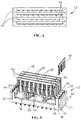
- FIG. 1is a perspective view of an illustrative backplane connector of the present invention with a mating daughtercard connector positioned above the backplane connector prior to mating therewith.
- FIG. 2is a perspective view of the backplane connector of the present invention mated with the daughtercard connector.
- FIG. 3is a perspective cross-sectional view of the daughtercard connector mated with the backplane connector, taken along line 3 - 3 of FIG. 2 .
- FIG. 4is a cross-sectional view of the daughtercard connector mated with the backplane connector, taken along line 4 - 4 of FIG. 2 .
- FIG. 5is a perspective view of the backplane connector with a clip exploded therefrom.
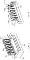
- FIG. 6is an exploded front perspective view of an overmolded chicklet or module of the backplane connector.
- FIG. 7is an exploded back perspective view of the overmolded chicklet or module of the backplane connector.
- FIG. 8is a front perspective view of a first alternate embodiment of a partially assembled backplane connector.
- FIG. 9is a front perspective view of a second alternate embodiment of a backplane connector.
- FIG. 1illustrates an electrical connector system 10 formed in accordance with an illustrative embodiment.
- the electrical connector system 10includes a backplane connector 12 and a daughtercard connector 14 that are used to electrically connect a backplane circuit board (not shown) and a daughtercard circuit board (not shown). While the electrical connector system 10 is described herein with reference to backplane connectors 12 and daughtercard connectors 14 , it is realized that the subject matter herein may be utilized with different types of electrical connectors other than a backplane connector or a daughtercard connector.
- the backplane connector 12 and the daughtercard connector 14are merely illustrative of an illustrative embodiment of an electrical connector system 10 that interconnects a particular type of circuit board, namely a backplane circuit board, with a daughtercard circuit board.
- the backplane connector 12constitutes a header connector mounted to the backplane circuit board.
- the backplane connector 12is mated to the daughtercard connector 14 .
- the daughtercard circuit boardis oriented generally perpendicular with respect to the backplane circuit board.
- the daughtercard connector 14constitutes a right angle connector wherein a mating interface 16 and mounting interface 18 of the daughtercard connector 14 are oriented perpendicular to one another.
- the daughtercard connector 14is mounted to the daughtercard circuit board at the mounting interface 18 .
- Other orientations of the interfaces 16 , 18are possible in alternative embodiments.
- the backplane connector 12includes a mating interface 20 and a mounting interface 22 that are oriented generally parallel to one another.
- the backplane connector 12is mounted to the backplane circuit board at the mounting interface 22 .
- Other orientations of the interfaces 20 , 22are possible in alternative embodiments.
- the daughtercard connector 14includes a housing 24 holding a plurality of circuit boards 26 therein.
- the circuit boards 26has pairs 28 of individual signal pathways or traces that extend between the mating interface 16 and the mounting interface 18 .
- the signal traceshave signal conductive pads 32 provided proximate the mating interface 16 .
- the signal conductive pads 32are configured to be mated with and electrically connected to the signal contacts 48 ( FIG. 6 ) of the backplane connector 12 .
- the circuit boards 26has individual ground pathways or traces that extend between the mating interface 16 and the mounting interface 18 .
- the ground traceshave ground conductive pads 34 provided proximate the mating interface 16 .
- the ground conductive pads 34are configured to be mated with, and electrically connected to, the ground contacts 52 ( FIG. 6 ) of the backplane connector 12 .
- the circuit boards 26may be contact modules, the signal traces may be mating signal contacts and the ground traces may be ground contacts.
- the backplane connector 12includes a housing 38 which is made from a plurality of modules 40 .
- Each of the modules 40has a mating end 42 , also referred to herein as a front 42 , that is loaded into recess 44 of the daughtercard connector 14 during mating.
- Each of the modules 40has a mounting end 46 , also referred to herein as a rear 46 , which is mounted to the backplane circuit board.
- each of the modules 40has a circuit board or substrate 45 which holds a plurality of individual signal pathways 47 which include mating signal contacts 48 , signal traces 49 and mounting signal contacts 50 .
- the mating signal contacts 48are mechanically and electrically connected to the signal traces 49 by known methods, such as but not limited to soldering to a conductive pad of the signal traces 49 .
- the mounting signal contacts 50are mechanically and electrically connected to the signal traces 49 by known methods, such as but not limited to soldering to a conductive pad of the signal traces 49 .
- the signal pathways 47extend between the mating end 42 and the mounting end 46 . In an exemplary embodiment, the signal pathways 47 are arranged in pairs carrying differential signals.
- the individual signal pathways 47are positioned on a first surface 55 of each module 40 .
- Each of the substrates 45 of the modules 40holds a plurality of first ground pathways 51 which include mating ground contacts 52 , ground traces 53 and mounting ground contacts 54 .
- Each of the plurality of ground pathways 51are positioned adjacent to at least one of the plurality of signal pathways 47 .
- the mating ground contacts 52are mechanically and electrically connected to the ground traces 53 by known methods, such as but not limited to soldering to a conductive pad of the ground traces 53 .
- the mounting ground contacts 54are mechanically and electrically connected to the ground traces 53 by known methods, such as but not limited to soldering to a conductive pad of the ground traces 53 .
- the ground pathways 51extend between the mating end 42 and the mounting end 46 .
- the individual ground pathways 51are positioned on the first surface 55 of each module 40 .
- Each of the substrates 45 of the modules 40include second ground pathways or traces 56 on a second surface 57 of each module 40 .
- the second surface 57being opposed and spaced from the first surface 55 .
- the second ground pathways or traces 56extend between the mating end 42 and the mounting end 46 .
- the individual ground pathways 51are positioned on the first surface 55 of each module 40 .
- the plurality of second ground pathways or traces 56are positioned in line with the plurality of the signal pathways 47 .
- Vias 58extend from ground traces 53 on the first surface 55 through the substrate 45 to ground traces 56 on the second surface 57 , thereby placing the ground traces 53 is electrical engagement with the ground traces 56 .
- the vias 58also providing shielding between pairs of the signal pathways 47 .
- ground traces 53 on the first surface 55The combination of the ground traces 53 on the first surface 55 , the ground traces 56 on the second surface 57 and the vias 58 form shielding cavities around the pairs of the signal pathways 47 .
- the spacing of the ground traces 53 , the ground traces 56 and the vias 58is optimized for impedance control, as well as shielding.
- Each of the modules 40has a contact protection member 59 which is positioned on the first surface 55 of the substrates 45 proximate the mating end 42 .
- the contact protection member 59extends from the first surface 55 in a direction away from the second surface 57 .
- the contact protection member 59has a lead-in surface 60 and mounting projections 61 .
- the mounting projections 61cooperate with openings 63 of the substrates 45 to maintain the contact protection member 59 on the substrates 45 .
- the contact protection member 59is overmolded on the substrate 45 , however, the contact protection member 59 may be positioned and maintained on the substrate 45 by other known methods.
- contact protection members 59 amay be provided, as for example as shown in FIG. 8 .
- the contact projections members 59 aare positioned on the first surface 55 a of the substrates 45 a proximate the mating end 42 a .
- the contact protection members 59 aextend from the first surfaces 55 a in a direction away from the second surfaces 57 a .
- the contact protection members 59 aeach have a lead-in surface 60 a and a mounting projection 61 a .
- the mounting projections 61 acooperate with opening 63 a of the substrates 45 a to maintain the contact protection members 59 a on the substrates 45 a .
- the contact protection members 59 aare overmolded on the substrates 45 a.
- the housing 38 of the backplane connector 12has four modules 40 which are positioned adjacent to each other.
- Circuit board receiving slots 62are provided between adjacent modules 40 .
- the circuit board receiving slots 62are positioned adjacent the contact protection members 59 of the modules 40 .
- Each circuit board receiving slot 62extends from the mating end 42 of the modules 40 toward the mounting end 46 .
- Each module 40has a base section 66 which extends from the mounting end 46 toward the mating end 42 .
- the base section 66has end sections 67 which extend beyond a connector receiving sections 64 , as shown in FIG. 5 .
- Each of the end sections 67has a clip receiving slot 68 which extends from a top surface 69 of the end section 67 toward the mounting end 46 .
- the base sections 66are overmolded on the substrates 45 , however, the base sections 66 may be positioned and maintained on the substrates 45 by other known methods.
- the base section 67 a of the housing 38 amay be one piece in which the substrates 45 a are mounted therein, as shown in FIG. 8 .
- clips 69are inserted into the clip receiving slots 68 to properly position and retain the modules 40 in position relative to each other.
- the clips 69may have cavities 70 provided therein which cooperate with projections (not shown) in the clip receiving slots 68 to more accurately position and maintain the modules 40 relative to each other.
- the mating signal contacts 48have mating contact receiving sections 71 and securing sections 72 .
- each of the contact receiving sections 71include two resilient arms 74 with lead in portions 75 and engagement portions 76 .
- the resilient arms 74are configured to press against the signal conductive pads 32 when the daughter card connector 14 is mated to the backplane connector 12 .
- the securing sections 72are configured to mount to the signal pathways 47 on the first surfaces 55 of the substrates 45 .
- the mounting signal contacts 50have mounting members 73 and compliant portions 78 .
- the mounting members 73are configured to mount to the signal pathways 47 on the first surfaces 55 of the substrates 45 .
- the compliant portions 78are configured to engage the printed circuit board (not shown).
- the compliant portions 78may be, but are not limited to, an eye of the needle pin, although other configurations may be used.
- the mating ground contacts 52have mating contact receiving sections 80 and securing sections 81 .
- each of the contact receiving sections 80include two resilient arms 83 with lead in portions 84 and engagement portions 85 .
- the resilient arms 83are configured to press against the ground conductive pads 34 when the daughter card connector 14 is mated to the backplane connector 12 .
- the securing sections 81are configured to mount to the ground pathways 52 on the first surfaces 55 of the substrates 45 .
- the mating ground contacts 52have mounting members 86 and compliant portions 87 .
- the mounting members 86are configured to mount to the ground pathways 52 on the first surfaces 55 of the substrates 45 .
- the compliant portions 87are configured to engage the printed circuit board (not shown).
- the compliant portions 87may be, but are not limited to, an eye of the needle pin, although other configurations may be used.
- the combination of the ground pathways 51 , the vias 58 and the ground traces 56entirely peripherally surround the pairs of signal pathways 47 .
- the ground pathways 51 , the vias 58 and the ground traces 56are electrically commoned together, the ground pathways 51 , the vias 58 and the ground traces 56 provide electrical shielding for the pairs of signal pathways 47 .
- Gaps or spaces, which could allow EMI leakage between pairs of signal pathways 47are minimal through or between the ground pathways 51 , the vias 58 and the ground traces 56 .
- the ground pathways 51 , the vias 58 and the ground traces 56extend along multiple pairs of signal pathways 47 .
- the ground pathways 51 , the vias 58 and the ground traces 56form cavities around the pairs of signal pathways 47 .
- the cavitiesmay have any shape depending on the shapes of the ground pathways 51 , the vias 58 and the ground traces 56 .
- the ground pathways 51 , the vias 58 and the ground traces 56extend about the periphery of the pairs of signal pathways 47 and surround the pairs of signal pathways 47 to provide electrical shielding for the pairs of signal pathways 47 .
- entire, 360 degree shieldingis provided by the ground pathways 51 , the vias 58 and the ground traces 56 along the length of the signal pathways 47 .
- the ground pathways 51 , the vias 58 and the ground traces 56also surround portions of the mating signal traces when the connectors 12 , 14 are mated.
- the ground pathways 51 , the vias 58 and the ground traces 56provide shielding along the entire mating interface with the mating signal traces.
- the ground pathways 51 , the vias 58 and the ground traces 56may control electrical characteristics at the mating interfaces 16 , 20 and throughout the housing 38 , such as by controlling cross talk, signal radiation, impedance or other electrical characteristics.
- the circuit boards 26 of the daughter card connector 14are positioned in the circuit board receiving slots 62 .
- the mating signal contacts 48 of the signal pathways 47 of the modules 40physically and electrically engage the signal conductive pads 32 of the signal traces of the circuit boards 26 .
- the mating ground contacts 52 of the ground pathways 51 of the modules 40are also placed in physical and electrical engagement with the ground conductive pads 34 of the ground traces of the circuit boards 26 .
- ground pathways 51 , the vias 58 and the ground traces 56provide shielding for the mating signal contacts 48 and the portions of the signal conductive pads 32 of the signal traces of the circuit boards 26 which are positioned in the circuit board receiving slots 62 of the modules 40 of the housing 38 of the backplane connector 12 .
- the signal contacts 48 b and the ground contacts 52 bare rotated 180 degrees from the illustrative embodiments shown in FIGS. 1 through 8 .
- the securing sections 81 b of the ground contacts 52 bextend from the first surface 55 b , around the mating end 42 b and are attached to the second surface 57 b of the substrate 45 b , thereby allowing the ground contacts 52 b to be placed in electrical engagement with the ground traces on both the first surface 55 b and the second surface 57 b of the substrate 45 b.
Landscapes
- Physics & Mathematics (AREA)
- Electromagnetism (AREA)
- Engineering & Computer Science (AREA)
- Microelectronics & Electronic Packaging (AREA)
- Details Of Connecting Devices For Male And Female Coupling (AREA)
Abstract
Description
Claims (19)
Priority Applications (2)
| Application Number | Priority Date | Filing Date | Title |
|---|---|---|---|
| US16/830,451US11297712B2 (en) | 2020-03-26 | 2020-03-26 | Modular printed circuit board wafer connector with reduced crosstalk |
| EP21163858.0AEP3886269B1 (en) | 2020-03-26 | 2021-03-22 | Modular printed circuit board wafer connector with reduced cross-talk |
Applications Claiming Priority (1)
| Application Number | Priority Date | Filing Date | Title |
|---|---|---|---|
| US16/830,451US11297712B2 (en) | 2020-03-26 | 2020-03-26 | Modular printed circuit board wafer connector with reduced crosstalk |
Publications (2)
| Publication Number | Publication Date |
|---|---|
| US20210307156A1 US20210307156A1 (en) | 2021-09-30 |
| US11297712B2true US11297712B2 (en) | 2022-04-05 |
Family
ID=75143463
Family Applications (1)
| Application Number | Title | Priority Date | Filing Date |
|---|---|---|---|
| US16/830,451Active2040-04-28US11297712B2 (en) | 2020-03-26 | 2020-03-26 | Modular printed circuit board wafer connector with reduced crosstalk |
Country Status (2)
| Country | Link |
|---|---|
| US (1) | US11297712B2 (en) |
| EP (1) | EP3886269B1 (en) |
Families Citing this family (1)
| Publication number | Priority date | Publication date | Assignee | Title |
|---|---|---|---|---|
| US11837828B2 (en)* | 2021-10-21 | 2023-12-05 | Dell Products L.P. | Memory module socket for an information handling system |
Citations (48)
| Publication number | Priority date | Publication date | Assignee | Title |
|---|---|---|---|---|
| US6171115B1 (en) | 2000-02-03 | 2001-01-09 | Tyco Electronics Corporation | Electrical connector having circuit boards and keying for different types of circuit boards |
| US6267604B1 (en) | 2000-02-03 | 2001-07-31 | Tyco Electronics Corporation | Electrical connector including a housing that holds parallel circuit boards |
| US6384341B1 (en) | 2001-04-30 | 2002-05-07 | Tyco Electronics Corporation | Differential connector footprint for a multi-layer circuit board |
| US6488549B1 (en) | 2001-06-06 | 2002-12-03 | Tyco Electronics Corporation | Electrical connector assembly with separate arcing zones |
| US6488544B1 (en)* | 2001-05-22 | 2002-12-03 | Hon Hai Precision Ind. Co., Ltd. | Anti crosstalk electrical connector and method of manufacturing the same |
| US6540522B2 (en) | 2001-04-26 | 2003-04-01 | Tyco Electronics Corporation | Electrical connector assembly for orthogonally mating circuit boards |
| US6582250B2 (en) | 2001-11-20 | 2003-06-24 | Tyco Electronics Corporation | Connector module organizer |
| US6641438B1 (en)* | 2002-06-07 | 2003-11-04 | Hon Hai Precision Ind. Co., Ltd. | High speed, high density backplane connector |
| US6655966B2 (en) | 2002-03-19 | 2003-12-02 | Tyco Electronics Corporation | Modular connector with grounding interconnect |
| US6663442B1 (en) | 2000-01-27 | 2003-12-16 | Tyco Electronics Corporation | High speed interconnect using printed circuit board with plated bores |
| US6663426B2 (en) | 2002-01-09 | 2003-12-16 | Tyco Electronics Corporation | Floating interface for electrical connector |
| US6676450B2 (en) | 2000-05-25 | 2004-01-13 | Tyco Electronics Corporation | Electrical connector having contacts isolated by shields |
| US6705895B2 (en) | 2002-04-25 | 2004-03-16 | Tyco Electronics Corporation | Orthogonal interface for connecting circuit boards carrying differential pairs |
| US20040094328A1 (en)* | 2002-11-16 | 2004-05-20 | Fjelstad Joseph C. | Cabled signaling system and components thereof |
| US6808399B2 (en) | 2002-12-02 | 2004-10-26 | Tyco Electronics Corporation | Electrical connector with wafers having split ground planes |
| US6808419B1 (en)* | 2003-08-29 | 2004-10-26 | Hon Hai Precision Ind. Co., Ltd. | Electrical connector having enhanced electrical performance |
| US6811440B1 (en) | 2003-08-29 | 2004-11-02 | Tyco Electronics Corporation | Power connector |
| US6811414B1 (en) | 2003-05-16 | 2004-11-02 | Tyco Electronics Corporation | Electrical connector module with multiple card edge sections |
| US6824391B2 (en) | 2000-02-03 | 2004-11-30 | Tyco Electronics Corporation | Electrical connector having customizable circuit board wafers |
| US6884117B2 (en)* | 2003-08-29 | 2005-04-26 | Hon Hai Precision Ind. Co., Ltd. | Electrical connector having circuit board modules positioned between metal stiffener and a housing |
| US6890214B2 (en) | 2002-08-21 | 2005-05-10 | Tyco Electronics Corporation | Multi-sequenced contacts from single lead frame |
| US6932649B1 (en) | 2004-03-19 | 2005-08-23 | Tyco Electronics Corporation | Active wafer for improved gigabit signal recovery, in a serial point-to-point architecture |
| US6945810B1 (en) | 2004-04-28 | 2005-09-20 | Tyco Electronics Corporation | Double ended guide pin for keying on both sides of a circuit board |
| US6964583B2 (en) | 2004-02-13 | 2005-11-15 | Tyco Electronics Corporation | Connector having low frequency noise reducing ground |
| US6997736B2 (en) | 2004-03-26 | 2006-02-14 | Tyco Electronics Corporation | Guide receptacle with tandem mounting features |
| US7044794B2 (en) | 2004-07-14 | 2006-05-16 | Tyco Electronics Corporation | Electrical connector with ESD protection |
| US7175445B2 (en) | 2004-08-31 | 2007-02-13 | Tyco Electronics Corporation | Electrical connector power wafers |
| US7201618B2 (en)* | 2005-01-28 | 2007-04-10 | Commscope Solutions Properties, Llc | Controlled mode conversion connector for reduced alien crosstalk |
| US20080038941A1 (en)* | 2006-08-11 | 2008-02-14 | Tyco Electronics Corporation | Circuit board having configurable ground link and with coplanar circuit and ground traces |
| US20100029105A1 (en)* | 2008-07-29 | 2010-02-04 | Tyco Electronics Corporation | Contact organizer for an electrical connector |
| US20100151741A1 (en)* | 2008-12-05 | 2010-06-17 | James Lee Fedder | Electrical Connector System |
| US20100151726A1 (en)* | 2008-12-05 | 2010-06-17 | James Lee Fedder | Electrical Connector System |
| US7967614B1 (en)* | 2010-04-28 | 2011-06-28 | Tyco Electronics Corporation | Plug connector and connector assembly having a pluggable board substrate |
| US8398432B1 (en)* | 2011-11-07 | 2013-03-19 | Tyco Electronics Corporation | Grounding structures for header and receptacle assemblies |
| US8657627B2 (en)* | 2011-02-02 | 2014-02-25 | Amphenol Corporation | Mezzanine connector |
| US20140154895A1 (en)* | 2012-07-05 | 2014-06-05 | Leviton Manufacturing Co., Inc. | High density high speed data communications connector |
| EP2752947A1 (en) | 2013-01-07 | 2014-07-09 | Tyco Electronics Corporation | Grounding structures for a receptacle assembly |
| US8840431B2 (en) | 2012-10-26 | 2014-09-23 | Tyco Electronics Corporation | Electrical connector systems |
| US20150194754A1 (en)* | 2014-01-09 | 2015-07-09 | Tyco Electronics Corporation | Configurable electrical connector assembly |
| US9831588B2 (en)* | 2012-08-22 | 2017-11-28 | Amphenol Corporation | High-frequency electrical connector |
| US9997868B1 (en)* | 2017-07-24 | 2018-06-12 | Te Connectivity Corporation | Electrical connector with improved impedance characteristics |
| US10050361B1 (en)* | 2017-05-22 | 2018-08-14 | Te Connectivity Corporation | Flexible circuit connector |
| US10128597B2 (en)* | 2016-06-10 | 2018-11-13 | Te Connectivity Corporation | Electrical contact pad for electrically contacting a connector |
| US20190296469A1 (en) | 2018-03-22 | 2019-09-26 | Amphenol Corporation | High density electrical connector |
| US10535971B2 (en) | 2017-10-12 | 2020-01-14 | Te Connectivity Corporation | Electrical connector |
| US10574000B1 (en)* | 2018-11-05 | 2020-02-25 | Te Connectivity Corporation | Grounding structure for an electrical connector |
| US20200176905A1 (en)* | 2017-05-15 | 2020-06-04 | Samtec, Inc. | Printed circuit board having commoned ground plane |
| US10763622B2 (en)* | 2018-11-05 | 2020-09-01 | Te Connectivity Corporation | Grounding structure for an electrical connector |
- 2020
- 2020-03-26USUS16/830,451patent/US11297712B2/enactiveActive
- 2021
- 2021-03-22EPEP21163858.0Apatent/EP3886269B1/enactiveActive
Patent Citations (48)
| Publication number | Priority date | Publication date | Assignee | Title |
|---|---|---|---|---|
| US6663442B1 (en) | 2000-01-27 | 2003-12-16 | Tyco Electronics Corporation | High speed interconnect using printed circuit board with plated bores |
| US6267604B1 (en) | 2000-02-03 | 2001-07-31 | Tyco Electronics Corporation | Electrical connector including a housing that holds parallel circuit boards |
| US6171115B1 (en) | 2000-02-03 | 2001-01-09 | Tyco Electronics Corporation | Electrical connector having circuit boards and keying for different types of circuit boards |
| US6824391B2 (en) | 2000-02-03 | 2004-11-30 | Tyco Electronics Corporation | Electrical connector having customizable circuit board wafers |
| US6676450B2 (en) | 2000-05-25 | 2004-01-13 | Tyco Electronics Corporation | Electrical connector having contacts isolated by shields |
| US6540522B2 (en) | 2001-04-26 | 2003-04-01 | Tyco Electronics Corporation | Electrical connector assembly for orthogonally mating circuit boards |
| US6384341B1 (en) | 2001-04-30 | 2002-05-07 | Tyco Electronics Corporation | Differential connector footprint for a multi-layer circuit board |
| US6488544B1 (en)* | 2001-05-22 | 2002-12-03 | Hon Hai Precision Ind. Co., Ltd. | Anti crosstalk electrical connector and method of manufacturing the same |
| US6488549B1 (en) | 2001-06-06 | 2002-12-03 | Tyco Electronics Corporation | Electrical connector assembly with separate arcing zones |
| US6582250B2 (en) | 2001-11-20 | 2003-06-24 | Tyco Electronics Corporation | Connector module organizer |
| US6663426B2 (en) | 2002-01-09 | 2003-12-16 | Tyco Electronics Corporation | Floating interface for electrical connector |
| US6655966B2 (en) | 2002-03-19 | 2003-12-02 | Tyco Electronics Corporation | Modular connector with grounding interconnect |
| US6705895B2 (en) | 2002-04-25 | 2004-03-16 | Tyco Electronics Corporation | Orthogonal interface for connecting circuit boards carrying differential pairs |
| US6641438B1 (en)* | 2002-06-07 | 2003-11-04 | Hon Hai Precision Ind. Co., Ltd. | High speed, high density backplane connector |
| US6890214B2 (en) | 2002-08-21 | 2005-05-10 | Tyco Electronics Corporation | Multi-sequenced contacts from single lead frame |
| US20040094328A1 (en)* | 2002-11-16 | 2004-05-20 | Fjelstad Joseph C. | Cabled signaling system and components thereof |
| US6808399B2 (en) | 2002-12-02 | 2004-10-26 | Tyco Electronics Corporation | Electrical connector with wafers having split ground planes |
| US6811414B1 (en) | 2003-05-16 | 2004-11-02 | Tyco Electronics Corporation | Electrical connector module with multiple card edge sections |
| US6808419B1 (en)* | 2003-08-29 | 2004-10-26 | Hon Hai Precision Ind. Co., Ltd. | Electrical connector having enhanced electrical performance |
| US6811440B1 (en) | 2003-08-29 | 2004-11-02 | Tyco Electronics Corporation | Power connector |
| US6884117B2 (en)* | 2003-08-29 | 2005-04-26 | Hon Hai Precision Ind. Co., Ltd. | Electrical connector having circuit board modules positioned between metal stiffener and a housing |
| US6964583B2 (en) | 2004-02-13 | 2005-11-15 | Tyco Electronics Corporation | Connector having low frequency noise reducing ground |
| US6932649B1 (en) | 2004-03-19 | 2005-08-23 | Tyco Electronics Corporation | Active wafer for improved gigabit signal recovery, in a serial point-to-point architecture |
| US6997736B2 (en) | 2004-03-26 | 2006-02-14 | Tyco Electronics Corporation | Guide receptacle with tandem mounting features |
| US6945810B1 (en) | 2004-04-28 | 2005-09-20 | Tyco Electronics Corporation | Double ended guide pin for keying on both sides of a circuit board |
| US7044794B2 (en) | 2004-07-14 | 2006-05-16 | Tyco Electronics Corporation | Electrical connector with ESD protection |
| US7175445B2 (en) | 2004-08-31 | 2007-02-13 | Tyco Electronics Corporation | Electrical connector power wafers |
| US7201618B2 (en)* | 2005-01-28 | 2007-04-10 | Commscope Solutions Properties, Llc | Controlled mode conversion connector for reduced alien crosstalk |
| US20080038941A1 (en)* | 2006-08-11 | 2008-02-14 | Tyco Electronics Corporation | Circuit board having configurable ground link and with coplanar circuit and ground traces |
| US20100029105A1 (en)* | 2008-07-29 | 2010-02-04 | Tyco Electronics Corporation | Contact organizer for an electrical connector |
| US20100151741A1 (en)* | 2008-12-05 | 2010-06-17 | James Lee Fedder | Electrical Connector System |
| US20100151726A1 (en)* | 2008-12-05 | 2010-06-17 | James Lee Fedder | Electrical Connector System |
| US7967614B1 (en)* | 2010-04-28 | 2011-06-28 | Tyco Electronics Corporation | Plug connector and connector assembly having a pluggable board substrate |
| US8657627B2 (en)* | 2011-02-02 | 2014-02-25 | Amphenol Corporation | Mezzanine connector |
| US8398432B1 (en)* | 2011-11-07 | 2013-03-19 | Tyco Electronics Corporation | Grounding structures for header and receptacle assemblies |
| US20140154895A1 (en)* | 2012-07-05 | 2014-06-05 | Leviton Manufacturing Co., Inc. | High density high speed data communications connector |
| US9831588B2 (en)* | 2012-08-22 | 2017-11-28 | Amphenol Corporation | High-frequency electrical connector |
| US8840431B2 (en) | 2012-10-26 | 2014-09-23 | Tyco Electronics Corporation | Electrical connector systems |
| EP2752947A1 (en) | 2013-01-07 | 2014-07-09 | Tyco Electronics Corporation | Grounding structures for a receptacle assembly |
| US20150194754A1 (en)* | 2014-01-09 | 2015-07-09 | Tyco Electronics Corporation | Configurable electrical connector assembly |
| US10128597B2 (en)* | 2016-06-10 | 2018-11-13 | Te Connectivity Corporation | Electrical contact pad for electrically contacting a connector |
| US20200176905A1 (en)* | 2017-05-15 | 2020-06-04 | Samtec, Inc. | Printed circuit board having commoned ground plane |
| US10050361B1 (en)* | 2017-05-22 | 2018-08-14 | Te Connectivity Corporation | Flexible circuit connector |
| US9997868B1 (en)* | 2017-07-24 | 2018-06-12 | Te Connectivity Corporation | Electrical connector with improved impedance characteristics |
| US10535971B2 (en) | 2017-10-12 | 2020-01-14 | Te Connectivity Corporation | Electrical connector |
| US20190296469A1 (en) | 2018-03-22 | 2019-09-26 | Amphenol Corporation | High density electrical connector |
| US10574000B1 (en)* | 2018-11-05 | 2020-02-25 | Te Connectivity Corporation | Grounding structure for an electrical connector |
| US10763622B2 (en)* | 2018-11-05 | 2020-09-01 | Te Connectivity Corporation | Grounding structure for an electrical connector |
Non-Patent Citations (1)
| Title |
|---|
| European Search Report, dated Aug. 26, 2021, EP 21 16 3858, European Application No. 21163858.0-1201. |
Also Published As
| Publication number | Publication date |
|---|---|
| EP3886269A1 (en) | 2021-09-29 |
| EP3886269B1 (en) | 2024-02-07 |
| US20210307156A1 (en) | 2021-09-30 |
Similar Documents
| Publication | Publication Date | Title |
|---|---|---|
| US11081821B2 (en) | Direct mate cable assembly | |
| US10741951B2 (en) | Socket connector assembly for an electronic package | |
| US10998678B1 (en) | Modular electrical connector with additional grounding | |
| CN102570104B (en) | Electric connector system | |
| US11025014B1 (en) | Shield component for use with modular electrical connector to reduce crosstalk | |
| US10868393B2 (en) | Electrical connector assembly for a communication system | |
| CN108365465A (en) | Electric connector with mating connector interface | |
| CN102176557A (en) | High density bottom plate connector | |
| US20090233492A1 (en) | Connector and Connector Device | |
| US7059907B2 (en) | Modular electrical connector | |
| US11031734B1 (en) | Modular electrical connector with reduced crosstalk | |
| US10965062B1 (en) | Modular electrical connector with conductive coating to reduce crosstalk | |
| US11297712B2 (en) | Modular printed circuit board wafer connector with reduced crosstalk | |
| US12322887B2 (en) | Circuit board wafer with contacts mounted on castellated edges | |
| US11264749B2 (en) | Modular connector with printed circuit board wafer to reduce crosstalk | |
| US20240047907A1 (en) | Cable assembly for a cable connector module | |
| US12407137B2 (en) | Ground shields positioned between columns of contacts | |
| US20240145968A1 (en) | Electrical Connector with Angled Contacts | |
| US12407138B2 (en) | Contact and shield configuration for ground current optimization | |
| US12334685B2 (en) | Interconnection system for ground current optimization | |
| US20240313476A1 (en) | Ground Shield Contact Member |
Legal Events
| Date | Code | Title | Description |
|---|---|---|---|
| FEPP | Fee payment procedure | Free format text:ENTITY STATUS SET TO UNDISCOUNTED (ORIGINAL EVENT CODE: BIG.); ENTITY STATUS OF PATENT OWNER: LARGE ENTITY | |
| AS | Assignment | Owner name:TE CONNECTIVITY SERVICES GMBH, SWITZERLAND Free format text:ASSIGNMENT OF ASSIGNORS INTEREST;ASSIGNORS:MILLER, KEITH EDWIN;TSANG, ALBERT;SIGNING DATES FROM 20200320 TO 20200331;REEL/FRAME:052333/0263 | |
| STPP | Information on status: patent application and granting procedure in general | Free format text:NON FINAL ACTION MAILED | |
| STPP | Information on status: patent application and granting procedure in general | Free format text:RESPONSE TO NON-FINAL OFFICE ACTION ENTERED AND FORWARDED TO EXAMINER | |
| STPP | Information on status: patent application and granting procedure in general | Free format text:NOTICE OF ALLOWANCE MAILED -- APPLICATION RECEIVED IN OFFICE OF PUBLICATIONS | |
| STPP | Information on status: patent application and granting procedure in general | Free format text:PUBLICATIONS -- ISSUE FEE PAYMENT VERIFIED | |
| STCF | Information on status: patent grant | Free format text:PATENTED CASE | |
| AS | Assignment | Owner name:TE CONNECTIVITY SOLUTIONS GMBH, SWITZERLAND Free format text:MERGER;ASSIGNOR:TE CONNECTIVITY SERVICES GMBH;REEL/FRAME:060305/0923 Effective date:20220301 | |
| MAFP | Maintenance fee payment | Free format text:PAYMENT OF MAINTENANCE FEE, 4TH YEAR, LARGE ENTITY (ORIGINAL EVENT CODE: M1551); ENTITY STATUS OF PATENT OWNER: LARGE ENTITY Year of fee payment:4 |