US11290188B2 - Fiber optical communication system using asymmetric optical waveguide splitter - Google Patents
Fiber optical communication system using asymmetric optical waveguide splitterDownload PDFInfo
- Publication number
- US11290188B2 US11290188B2US17/260,898US201917260898AUS11290188B2US 11290188 B2US11290188 B2US 11290188B2US 201917260898 AUS201917260898 AUS 201917260898AUS 11290188 B2US11290188 B2US 11290188B2
- Authority
- US
- United States
- Prior art keywords
- waveguide
- optical
- tap
- latchable
- recited
- Prior art date
- Legal status (The legal status is an assumption and is not a legal conclusion. Google has not performed a legal analysis and makes no representation as to the accuracy of the status listed.)
- Active
Links
- 230000003287optical effectEffects0.000titleclaimsabstractdescription141
- 238000004891communicationMethods0.000titleabstractdescription7
- 239000000835fiberSubstances0.000titledescription14
- 239000013307optical fiberSubstances0.000claimsabstractdescription21
- 238000010079rubber tappingMethods0.000claimsabstractdescription17
- 239000000758substrateSubstances0.000claimsdescription69
- 230000008878couplingEffects0.000claimsdescription33
- 238000010168coupling processMethods0.000claimsdescription33
- 238000005859coupling reactionMethods0.000claimsdescription33
- 230000007246mechanismEffects0.000claimsdescription24
- 238000005253claddingMethods0.000claimsdescription15
- 229910000679solderInorganic materials0.000claimsdescription14
- 230000005540biological transmissionEffects0.000description14
- VYPSYNLAJGMNEJ-UHFFFAOYSA-NSilicium dioxideChemical compoundO=[Si]=OVYPSYNLAJGMNEJ-UHFFFAOYSA-N0.000description7
- 238000013459approachMethods0.000description6
- 238000005516engineering processMethods0.000description6
- 238000010438heat treatmentMethods0.000description6
- 238000013519translationMethods0.000description5
- 238000012986modificationMethods0.000description4
- 230000004048modificationEffects0.000description4
- 230000008859changeEffects0.000description3
- 230000001419dependent effectEffects0.000description3
- 238000000926separation methodMethods0.000description3
- 239000000377silicon dioxideSubstances0.000description3
- 229910052581Si3N4Inorganic materials0.000description2
- XUIMIQQOPSSXEZ-UHFFFAOYSA-NSiliconChemical compound[Si]XUIMIQQOPSSXEZ-UHFFFAOYSA-N0.000description2
- 239000000463materialSubstances0.000description2
- 229910052710siliconInorganic materials0.000description2
- 239000010703siliconSubstances0.000description2
- 235000012239silicon dioxideNutrition0.000description2
- HQVNEWCFYHHQES-UHFFFAOYSA-Nsilicon nitrideChemical compoundN12[Si]34N5[Si]62N3[Si]51N64HQVNEWCFYHHQES-UHFFFAOYSA-N0.000description2
- 230000004913activationEffects0.000description1
- 230000008901benefitEffects0.000description1
- -1but not limited toSubstances0.000description1
- 238000006880cross-coupling reactionMethods0.000description1
- 238000006073displacement reactionMethods0.000description1
- 230000000694effectsEffects0.000description1
- 230000005684electric fieldEffects0.000description1
- 239000012530fluidSubstances0.000description1
- 239000005350fused silica glassSubstances0.000description1
- 238000011065in-situ storageMethods0.000description1
- 238000002844meltingMethods0.000description1
- 230000008018meltingEffects0.000description1
- 238000000034methodMethods0.000description1
- 238000004806packaging method and processMethods0.000description1
- 230000002085persistent effectEffects0.000description1
- 230000008569processEffects0.000description1
- 230000001681protective effectEffects0.000description1
- 238000012552reviewMethods0.000description1
- 238000010561standard procedureMethods0.000description1
- 230000002459sustained effectEffects0.000description1
Images


Classifications
- H—ELECTRICITY
- H04—ELECTRIC COMMUNICATION TECHNIQUE
- H04B—TRANSMISSION
- H04B10/00—Transmission systems employing electromagnetic waves other than radio-waves, e.g. infrared, visible or ultraviolet light, or employing corpuscular radiation, e.g. quantum communication
- H04B10/27—Arrangements for networking
- H—ELECTRICITY
- H04—ELECTRIC COMMUNICATION TECHNIQUE
- H04B—TRANSMISSION
- H04B10/00—Transmission systems employing electromagnetic waves other than radio-waves, e.g. infrared, visible or ultraviolet light, or employing corpuscular radiation, e.g. quantum communication
- H04B10/25—Arrangements specific to fibre transmission
- H04B10/2589—Bidirectional transmission
- H04B10/25891—Transmission components
- G—PHYSICS
- G02—OPTICS
- G02B—OPTICAL ELEMENTS, SYSTEMS OR APPARATUS
- G02B6/00—Light guides; Structural details of arrangements comprising light guides and other optical elements, e.g. couplings
- G02B6/24—Coupling light guides
- G02B6/26—Optical coupling means
- G02B6/35—Optical coupling means having switching means
- G02B6/3502—Optical coupling means having switching means involving direct waveguide displacement, e.g. cantilever type waveguide displacement involving waveguide bending, or displacing an interposed waveguide between stationary waveguides
- G02B6/3508—Lateral or transverse displacement of the whole waveguides, e.g. by varying the distance between opposed waveguide ends, or by mutual lateral displacement of opposed waveguide ends
- G—PHYSICS
- G02—OPTICS
- G02F—OPTICAL DEVICES OR ARRANGEMENTS FOR THE CONTROL OF LIGHT BY MODIFICATION OF THE OPTICAL PROPERTIES OF THE MEDIA OF THE ELEMENTS INVOLVED THEREIN; NON-LINEAR OPTICS; FREQUENCY-CHANGING OF LIGHT; OPTICAL LOGIC ELEMENTS; OPTICAL ANALOGUE/DIGITAL CONVERTERS
- G02F1/00—Devices or arrangements for the control of the intensity, colour, phase, polarisation or direction of light arriving from an independent light source, e.g. switching, gating or modulating; Non-linear optics
- G02F1/29—Devices or arrangements for the control of the intensity, colour, phase, polarisation or direction of light arriving from an independent light source, e.g. switching, gating or modulating; Non-linear optics for the control of the position or the direction of light beams, i.e. deflection
- G02F1/31—Digital deflection, i.e. optical switching
- G02F1/313—Digital deflection, i.e. optical switching in an optical waveguide structure
- G02F1/3132—Digital deflection, i.e. optical switching in an optical waveguide structure of directional coupler type
- H—ELECTRICITY
- H04—ELECTRIC COMMUNICATION TECHNIQUE
- H04B—TRANSMISSION
- H04B10/00—Transmission systems employing electromagnetic waves other than radio-waves, e.g. infrared, visible or ultraviolet light, or employing corpuscular radiation, e.g. quantum communication
- H04B10/50—Transmitters
- H04B10/501—Structural aspects
- H04B10/503—Laser transmitters
- H—ELECTRICITY
- H04—ELECTRIC COMMUNICATION TECHNIQUE
- H04B—TRANSMISSION
- H04B10/00—Transmission systems employing electromagnetic waves other than radio-waves, e.g. infrared, visible or ultraviolet light, or employing corpuscular radiation, e.g. quantum communication
- H04B10/80—Optical aspects relating to the use of optical transmission for specific applications, not provided for in groups H04B10/03 - H04B10/70, e.g. optical power feeding or optical transmission through water
- G—PHYSICS
- G02—OPTICS
- G02B—OPTICAL ELEMENTS, SYSTEMS OR APPARATUS
- G02B6/00—Light guides; Structural details of arrangements comprising light guides and other optical elements, e.g. couplings
- G02B6/10—Light guides; Structural details of arrangements comprising light guides and other optical elements, e.g. couplings of the optical waveguide type
- G02B6/12—Light guides; Structural details of arrangements comprising light guides and other optical elements, e.g. couplings of the optical waveguide type of the integrated circuit kind
- G02B2006/12133—Functions
- G02B2006/1215—Splitter
Definitions
- the present inventionis generally directed to optical communications, and more specifically to optical splitters used for splitting a signal from a trunk fiber to a user.
- Passive optical networksare becoming prevalent in part because service providers want to deliver high bandwidth communication capabilities to customers. Passive optical networks are a desirable choice for delivering high-speed communication data because they may not employ active electronic devices, such as amplifiers and repeaters, between a central office and a subscriber termination. The absence of active electronic devices may decrease network complexity and/or cost and may increase network reliability.
- FIG. 1illustrates one embodiment of a network 100 deploying fiber optic lines.
- the network 100can include a central office 101 that connects a number of end subscribers 105 (also called end users 105 herein) in a network.
- the central office 101can additionally connect to a larger network such as the Internet (not shown) and a public switched telephone network (PSTN).
- PSTNpublic switched telephone network
- the network 100can also include fiber distribution hubs (FDHs) 103 that distribute signals to the end users 105 .
- the various lines of the network 100can be aerial or housed within underground conduits.
- the portion of the network 100 that is closest to central office 101is generally referred to as the F 1 region, where F 1 is the “feeder fiber” from the central office 101 .
- the portion of the network 100 closest to the end users 105can be referred to as an F 2 portion of network 100 .
- the network 100includes a plurality of break-out locations 102 at which branch cables are separated out from the main cable lines. Branch cables are often of the fibers of the branch cables to a plurality of different subscriber locations 105 .
- An incoming signalis received from the central office 101 , and is then typically split at the FDH 103 , using one or more optical splitters (e.g., 1 ⁇ 8 splitters, 1 ⁇ 16 splitters, or 1 ⁇ 32 splitters) to generate different user signals that are directed to the individual end users 105 .
- an optical splitteris provided prepackaged in an optical splitter module housing and provided with a splitter output in pigtails that extend from the module.
- the optical splitter moduleprovides protective packaging for the optical splitter components in the housing and thus provides for easy handling for otherwise fragile splitter components. This modular approach allows optical splitter modules to be added incrementally to FDHs 103 as required.
- a central office 202that includes a laser transmitter system 202 a and laser receiver system 202 b , distributes an optical signal to four users 204 in an optical network 206 via serially arranged asymmetric splitter modules 208 .
- the laser transmitter system 202 amay include one or more lasers producing optical signals at different wavelengths, which are multiplexed together, for example via wavelength division multiplexing (WDM) for transmission along the optical network 206 .
- the laser receiver system 202 bmay include one or more optical detectors that receive optical signals at different wavelengths. For example, after receiving a WDM optical signal from the optical network 206 , the laser receiver system 202 b may demultiplex the WDM signal and detect the optical signals at different wavelengths separately from each other.
- WDMwavelength division multiplexing
- the optical splitter modules 208 a , 208 b , 208 crespectively split off 1 ⁇ 4, 1 ⁇ 3 and 1 ⁇ 2 of the incident optical power.
- the tapping fractions of the splitter modules 208 a , 208 b and 208 care respectively 1 ⁇ 4, 1 ⁇ 3 and 1 ⁇ 2.
- the optical splitter modules 208each split off a fixed fraction of the incident optical power.
- the technician installing the optical splitter modulesmust be supplied with a variety of optical splitter modules, that split off different module is to be located.
- the larger the number of optical splitter modules placed serially along the networkthe greater the number of different splitter modules need to be carried in inventory.
- the present inventionis directed to an optical splitter module whose splitting faction can be adjusted in the field, and thereafter remains persistent. In this manner, the technician can carry just one type of optical splitter module, and adjust the splitting fraction in situ to the desired level.
- One embodiment of the inventionis directed to an optical system that includes a laser transmitter system to generate an optical signal and a first optical fiber network coupled to transmit the optical signal from the laser transmitter system.
- a first latchable, asymmetric coupleris disposed along the first optical fiber network to receive the optical signal, and is configured and arranged with a first tap output that receives a selected and alterable first fraction of the optical signal incident at the first latchable, asymmetric coupler.
- a second latchable, asymmetric coupleris disposed along the first optical fiber network to receive the optical signal from the first latchable asymmetric coupler.
- the second latchable, asymmetric coupleris configured and arranged with a second tap output that receives a selected and alterable second fraction of the optical signal incident at the second latchable, asymmetric coupler, the second fraction being different from the first fraction.
- Another embodiment of the inventionis directed to an optical system that includes a laser transmitter system to generate an optical signal and a first optical fiber network coupled to transmit the optical signal from the laser transmitter system.
- a first latchable, asymmetric coupleris disposed along the first optical fiber network to receive the optical signal, the first latchable, asymmetric coupler capable of operating at any of at least three different tapping fractions.
- a second latchable, asymmetric coupleris disposed along the first optical fiber network to receive the optical signal from the first latchable asymmetric coupler. The second latchable, asymmetric coupler is capable of operating at any of at least three different tapping fractions.
- FIG. 1schematically illustrates various elements of an optical data distribution and communication network
- FIG. 2schematically illustrates a simple, serial optical network having four users and the different optical splitter modules required to provide optical signals of equal magnitude to each user;
- FIG. 3schematically illustrates an embodiment of a latchable, asymmetric adjustable waveguide splitter, according to an embodiment of the present invention
- FIGS. 4A-4Bschematically illustrate an embodiment of a latchable, asymmetric adjustable waveguide splitter in a first configuration, according to an embodiment of the present invention
- FIGS. 4C-4Dschematically illustrate an embodiment of a latchable, asymmetric adjustable waveguide splitter in a second configuration, according to an embodiment of the present invention
- FIG. 4Eschematically illustrates an embodiment of a latchable, asymmetric adjustable waveguide splitter with optical fiber input and outputs, according to an embodiment of the present invention
- FIGS. 5A and 5Bschematically illustrate a latchable, asymmetric adjustable waveguide splitter, according to another embodiment of the present invention
- FIGS. 6A and 6Bschematically illustrate a latchable, asymmetric adjustable waveguide splitter, according to another embodiment of the present invention
- FIGS. 7A and 7Bschematically illustrate an embodiment of a latchable asymmetric adjustable waveguide splitter having a ratcheted translation mechanism, according to an embodiment of the present invention
- FIGS. 7C and 7Dschematically illustrate an embodiment of a latchable asymmetric adjustable waveguide splitter having a hydraulic translation mechanism, according to an embodiment of the present invention
- FIGS. 8A and 8Bschematically illustrate an embodiment of a latchable asymmetric adjustable waveguide splitter having a lockable translation mechanism, according to an embodiment of the present invention
- FIGS. 9A and 9Bschematically illustrate an embodiment of a latchable asymmetric adjustable waveguide splitter having a cantilevered translation mechanism, according to an embodiment of the present invention
- FIG. 10schematically illustrates an embodiment of a latchable asymmetric adjustable waveguide splitter having a splitter network, according to an embodiment of the present invention
- FIG. 11schematically illustrates a model coupler employed in analysis of a latchable asymmetric adjustable waveguide splitter
- FIGS. 12A and 12Brespectively present results of splitter transmission as a function of wavelength and power flow in the coupler, for a gap size of 6 ⁇ m;
- FIGS. 13A and 13Brespectively present results of splitter transmission as a function of wavelength and power flow in the coupler, for a gap size of 8 ⁇ m;
- FIGS. 14A and 14Brespectively present results of splitter transmission as a function of wavelength and power flow in the coupler, for a gap size of 9 ⁇ m;
- FIGS. 15A and 15Brespectively present results of splitter transmission as a function of wavelength and power flow in the coupler, for a gap size of 10 ⁇ m;
- FIGS. 16A and 16Brespectively present results of splitter transmission as a function of wavelength and power flow in the coupler, for a gap size of 11 ⁇ m;
- FIGS. 17A and 17Brespectively present results of splitter transmission as a function of wavelength and power flow in the coupler, for a gap size of 12 ⁇ m;
- FIGS. 18A and 18Brespectively present results of splitter transmission as a function of wavelength and power flow in the coupler, for a gap size of 16 ⁇ m;
- FIG. 19presents results of splitter transmission as a function of gap size for a wavelength of 1550 nm.
- the present inventionis directed to providing an asymmetric splitter than has a tunable splitting ratio that latches to a desired value for sustained operation with a selected tap ratio.
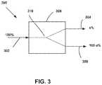
- FIG. 3schematically illustrates an embodiment of a latchable, asymmetric splitter module 300 . It has an input 302 , a tap output 304 and a main output 306 .
- the tap output 304constitutes the output that is directed off the main trunk, e.g. to one or more users, while the main output 306 is the output along the main trunk to the next splitter module.
- Each of the input, 302 , the tap output 304 and the main output 306may be provided as fiber pigtails.
- a splitter network 310which directs a portion (x %) of the light entering the splitter module 300 via in the input 302 to the tap output 304 , with the remaining light (100-x %) passing to the main output 306 .
- the tapping fractioni.e. that fraction of incoming light directed to the tap output 304 by the splitter, x %, is adjustable so that the power split ratio can be configured to a desired value.
- the splitter module 300includes an active embedded controller that, via a configuration tool used by a technician, adjusts the tapping fraction. Once the tapping fraction has been set, the tapping fraction may remain latched at the desired value until it is reset.
- the splitter module 300can remain at a specific tapping ratio until the optical network is changed, e.g. via the addition of customers, in which case the splitter ratio can be changed to accommodate the updates to the network.
- the splitter modulecan operate at any one of three or more tapping fractions, in other embodiments at any one of five or more tapping fractions, and in other embodiments, any one of seven or more tapping fractions.
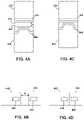
- FIGS. 4A-4Dschematically illustrate one approach to providing a latchable, asymmetric splitter module 400 .
- the splitter module 400includes a first substrate 402 and a second substrate 404 .
- the first and second substrates 402 , 404are arranged so as to permit relative motion of one or other of the substrates 402 , 404 .
- the first substrate 402includes a first waveguide 406 and the second substrate includes a second waveguide 408 .
- the first waveguide 406 and the second waveguide 408are arranged such that, under specific circumstances discussed below, light may couple from the first waveguide 406 to the second waveguide 408 .
- at least a portion of the first waveguide 406is located close to the first edge 410 of the first substrate 402 .
- at least a portion of the second waveguide 408is located close to the first edge 412 of the second substrate 404 .
- FIG. 4Bshows the same view in cross-section.
- the amount of light coupled between the first and second waveguides 402 , 404is dependent, inter alia, on the separation between the waveguides 402 , 404 . Accordingly, changing the separation distance, ⁇ , between the waveguides 402 , 404 , results in a change in the amount of light coupled from the first waveguide 402 to the second waveguide 404 .
- ⁇the separation distance between the waveguides 402 , 404
- asymmetric couplercan be set to a desired value.
- the waveguides 402 , 404may be formed using any suitable type of waveguide technology, including, for example, silicon, silicon nitride and silicon dioxide-based waveguides.
- Lightmay be directed into and out of the waveguides 406 , 408 using optical fibers attached to their respective substrates.
- the first substrate 402has a first input fiber 420 and a first output fiber 422
- the second substrate 404has a second input fiber 424 and a second output fiber 426 .
- the second input fiber 424may be omitted.
- the input and output fibers 420 , 422 , 424 , 426may be attached to their respective substrates via standard techniques, e.g., via a v-groove aligner block or the like.
- the substrates carrying the waveguidesmay be translated in different ways so as to effect a change in the optical coupling between waveguides.
- the approach shown in FIGS. 4A-4Ecan be described as a lateral translation to affect lateral coupling, i.e. the lateral direction of the motion of the substrates is parallel to the lateral direction of the coupling of light from one waveguide to the other.
- the substratesmay be arranged for vertical light coupling from one waveguide to the other, while there is lateral relative motion between the substrates.
- the first substrate 502 substrateis positioned below the second substrate 504 . In FIG.
- the second waveguide 508 in the second substrate 504is not positioned vertically above the first waveguide 506 in the first substrate 502 but is, instead, positioned to the side of the vertical position. In such a position there relatively weak, or even zero, optical coupling between the waveguides 506 , 508 .
- FIG. 5Bshows relatively strong optical coupling between the waveguides 506 , 508 .
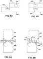
- the first substrate 602contains the first waveguide 606 and the second substrate contains a second waveguide 608 .
- the second substrate 604is located above the first substrate 602 , hence the first substrate 602 and first waveguide 606 are shown in dashed lines, while the second substrate 604 and second waveguide 608 are shown in solid lines.
- the first waveguide 602includes a coupling section 610 that lies closer to the edge 612 of the first substrate 602 than the remainder of the first waveguide 606 .
- the second waveguide 608includes a coupling section 614 that lies closer to the edge 616 of the second substrate 604 than the remainder of the second waveguide 608 .
- FIG. 6Ashows the first and second substrates 602 , 604 positioned to maximize the overlap between the coupling sections 610 , 614 of the first and second waveguides 606 , 608 .
- This positioncorresponds to a relatively high level of optical coupling between the first and second waveguides 606 , 608 .
- FIG. 6Bshows the second substrate 604 displaced in a direction parallel to the second coupling section 614 , so that first coupling section 610 overlaps with the second coupling section 614 over a shorter length, L, than in FIG. 6A .
- This positioncorresponds to a relatively smaller level of optical coupling between the waveguides 606 , 608 .
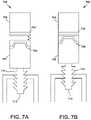
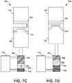
- FIGS. 7A and 7BAnother embodiment of part of a latchable, asymmetric splitter unit 700 is schematically, that uses microelectromechanical system (MEMS) technology is illustrated in FIGS. 7A and 7B .
- the splitter unit 700includes a first waveguide 702 mounted on a substrate 704 and a second waveguide 706 mounted on a movable substrate 708 .
- the movable substrate 708is movable in a direction transverse to the waveguides 702 , 706 .
- the movable substrate 708is connected to a ratchet element 710 provided with a set of ratchet teeth 712 .
- Engaging elements 714selectively engage the ratchet teeth 712 , both to permit the movable substrate 708 to slide in the direction shown by the double headed arrow, thus affecting the optical coupling between the first and second waveguides 702 , 706 , and to fix the movable substrate 708 at a desired position associated with the desired amount of optical coupling between the waveguides 702 , 706 .
- Optical fibersare not shown attached to the first and second waveguides 702 , 706 .
- the gap between the waveguides 702 , 706is large, corresponding to reduced gap between the waveguides 702 , 706 is reduced, corresponding to increased coupling between the waveguides 702 , 706 .
- FIGS. 7C and 7DAnother embodiment of part of a latchable, asymmetric splitter unit 750 , that uses microfluidic technology, is schematically illustrated in FIGS. 7C and 7D .
- the splitter unit 750includes a first waveguide 752 mounted on a substrate 754 and a second waveguide 756 mounted on a movable substrate 758 .
- the movable substrate 758is movable in a direction transverse to the waveguides 752 , 756 .
- the movable substrate 758is connected to a hydraulic element 760 that includes a piston 762 within a cylinder 764 .
- the piston 762is movable within the cylinder 764 to change the first volume 766 , single-hatched, on one side of the piston 762 , and the second volume 768 , cross-hatched, on the other side of the piston.
- a microfluidic management system 770is connected to the hydraulic element 760 to control the amount of hydraulic fluid in the first volume 766 and the second volume 768 , and thus control the position of the second waveguide 756 relative to the first waveguide 752 .
- Optical fibers, not shown,may be attached to the first and second waveguides 702 , 706 . In the embodiment illustrated in FIG.
- the gap between the waveguides 752 , 756is large, corresponding to reduced coupling between the waveguides 752 , 756 .
- the gap between the waveguides 752 , 756is reduced, corresponding to increased coupling between the waveguides 752 , 756 .
- FIGS. 8A and 8BAnother embodiment of part of a latchable, asymmetrical splitter unit 800 is schematically illustrated in FIGS. 8A and 8B .
- the splitter unit 800includes a lower substrate 802 and an upper substrate 804 .
- the lower substrate 802is provided with at least a first waveguide cladding 806 which is cladding to a first waveguide 808 .
- the first waveguide cladding 806 and first waveguide 808maybe formed on the first substrate 802 directly, using planar lithographic technology.
- the first waveguide cladding 806 and first waveguide 808may be formed on a preliminary substrate (not shown) that is subsequently attached to the first substrate 802 .
- the waveguide 808may be based on any suitable optical material including, but not limited to, silicon, silicon nitride and silicon dioxide.
- the second substrate 804is provided with a second waveguide cladding 810 and second waveguide 812 .
- the second waveguide cladding 810 and second waveguide 812maybe formed on the second substrate 804 directly using planar lithographic technology, or may be first formed substrate 804 .
- the second substrate 804is horizontally translatable relative to the first substrate 802 via a MEMS translating actuator (not shown).
- the first and second substrates 802 , 804are provided with respective solder supports 814 , 816 . Portions of solder 818 are located between the solder supports 814 , 816 .
- Heating elements 820are provided close to the solder supports 814 , 816 .
- the heating elements 820may formed of any suitable type of element that provides localized heating, such as resistive wires.
- the heating elements 820may be provided on, or close to, the solder supports 814 , 816 .
- the heating elements 820can be activated so as to melt the solder portions 818 when actuation of the asymmetrical splitter unit 800 is desired. Once the solder portions 818 have been melted, the MEMS translating actuator can move the second substrate 804 relative to the first substrate 802 by an amount that selects a desired fraction of optical power to be tapped from the main line. Once the unit 800 is operating with the desired tap fraction, as set by a relative displacement between the two waveguides 808 , 812 , the heating elements 820 can be deactivated. This allows the solder portions 818 to solidify, thus fixing the second substrate's position relative to the first substrate 802 , which latches the tap fraction at the desired value. FIG.
- FIG. 8Ashows a configuration where the second waveguide 812 is positioned above the first waveguide 808 , which corresponds with a relatively large level of optical coupling between the two waveguides 808 , 812 .
- FIG. 8Bshows a configuration where the second waveguide 812 has been laterally translated from the vertical position of FIG. 8A , so that there is a lower level of optical coupling between the waveguides 808 , 812 .
- FIGS. 9A and 9BAnother embodiment of part of a latchable, asymmetrical splitter unit 900 is schematically illustrated in FIGS. 9A and 9B .
- the unit 900has a substrate 902 that is provided with a step 904 .
- a first waveguide 906On top of the step 904 is a first waveguide 906 in a first waveguide cladding 908 .
- the first waveguide cladding 908 and the first waveguide 906maybe formed on the substrate 902 directly, using planar lithographic technology.
- a cantilevered portion 910that includes a second waveguide 912 in a second waveguide cladding 914 on a cantilever 916 .
- the cantilever 916is attached at one end to a cantilever support 918 .
- the cantilever 916is a MEMS-activatable via application of an electric field to displace downwards.
- the second waveguide 912In a first position, as shown in FIG. 9A , the second waveguide 912 is level with the first waveguide 906 .
- the first waveguide 906In a second the first waveguide 906 , resulting in reduced optical coupling between the waveguides 906 , 912 than in the configuration shown in FIG. 9A .
- Portions of solder 920 below the cantilever 916provide support and can have their height changed by melting the solder 920 before activation of the cantilever 916 .
- the optical signal coupled into the tap waveguidemay be sent directly into an optical fiber for transmission.
- the tap waveguidemay serve as an input to a waveguide splitter network, with the tapped optical signal being split into parts that are directed to individual optical fibers.
- FIG. 10A first substrate 1002 includes a first waveguide 1004 that receives the full optical signal (100%).
- the output from the first waveguide 1004is (100-x) % of the input signal.
- the value of xis selected for the specific application by adjusting the relative positions of the first waveguide 1004 and the tap waveguide 1008 , as discussed above.
- the tap waveguide 1008is coupled to a splitter network 1010 , having a number of outputs 1012 .
- the splitter network 1010splits the input signal into four signals of equal magnitude, and so the optical signal at each output 1012 is x/4%. It will be appreciated that the splitter network 1010 may include a different number of outputs 1012 , for example 2, 8 or 16 outputs, and that the fraction of light sent to different outputs 1012 need not be the same for all outputs 1012 .
- the optical coupling between two waveguideshas been numerically modeled.
- the waveguide structure assumed for the analysisis as shown in FIG. 11 .
- the height of the waveguideswas assumed to be 7 ⁇ m.
- the tap waveguide 1104was assumed to have a width that was constant along its length, 2 ⁇ m.
- the minimum center-to-center spacing between the two waveguides 1102 , 1104was measured at the center of the coupler.
- the material assumed for the claddingwas fused silica, having a refractive index of 1.444 at 1550 nm. It was assumed doped silica having a refractive index of about 1.451 at 1550 nm.
- FIGS. 12A-18Bpresent results of the analysis for various values of the minimum center-to-center spacing, g.
- Two data plotsare presented for each value of “g.”
- the figures denoted “A”e.g. FIGS. 12A, 13A etc.
- Each plotshows two curves—each curve labeled “A” represents the output from the main waveguide, while each curve labeled “B” represents the output from the tap waveguide.
- the powerwas calculated for an even split of the optical power into the TE mode and the TM mode.
- the figures denoted “B”present a plot of optical power within the coupler in the TEA mode, at 1460 nm.
- the curve “B,” which represents the power out of the tap waveguide 1104is flat with a value of almost zero dB across the wavelength range.
- Curve “A,” which represents the power out of the main waveguide 1102is less than 21 dB across the entire wavelength range. This is confirmed in the power plot of FIG. 12B , which shows virtually all the optical power in the tap waveguide.
- FIGS. 13A and 13B to FIGS. 18A and 18Bshow similar data but for different values of “g”.
- FIG. 19shows a plot of transmission at 1550 nm as a function of “g.”
- the level of coupling from the main waveguide to the tap waveguidechanges almost 100% with “g” varying over about 10 ⁇ m. Accordingly, the range of motion for values that would be used in a latchable, asymmetric coupler.
- the present inventionis applicable to fiber optical communication and data transmission systems. Accordingly, the present invention should not be considered limited to the particular examples described above, but rather should be understood to cover all aspects of the invention as fairly set out in the attached claims.
Landscapes
- Physics & Mathematics (AREA)
- Engineering & Computer Science (AREA)
- Electromagnetism (AREA)
- Computer Networks & Wireless Communication (AREA)
- Signal Processing (AREA)
- Optics & Photonics (AREA)
- Nonlinear Science (AREA)
- General Physics & Mathematics (AREA)
- Computing Systems (AREA)
- Optical Couplings Of Light Guides (AREA)
Abstract
Description
Claims (20)
Priority Applications (1)
| Application Number | Priority Date | Filing Date | Title |
|---|---|---|---|
| US17/260,898US11290188B2 (en) | 2018-07-17 | 2019-07-17 | Fiber optical communication system using asymmetric optical waveguide splitter |
Applications Claiming Priority (3)
| Application Number | Priority Date | Filing Date | Title |
|---|---|---|---|
| US201862699480P | 2018-07-17 | 2018-07-17 | |
| US17/260,898US11290188B2 (en) | 2018-07-17 | 2019-07-17 | Fiber optical communication system using asymmetric optical waveguide splitter |
| PCT/US2019/042188WO2020018657A1 (en) | 2018-07-17 | 2019-07-17 | Fiber optical communication system using asymmetric optical waveguide splitter |
Related Parent Applications (1)
| Application Number | Title | Priority Date | Filing Date |
|---|---|---|---|
| PCT/US2019/042188A-371-Of-InternationalWO2020018657A1 (en) | 2018-07-17 | 2019-07-17 | Fiber optical communication system using asymmetric optical waveguide splitter |
Related Child Applications (1)
| Application Number | Title | Priority Date | Filing Date |
|---|---|---|---|
| US17/675,818ContinuationUS11664900B2 (en) | 2018-07-17 | 2022-02-18 | Fiber optical communication system using asymmetric optical waveguide splitter |
Publications (2)
| Publication Number | Publication Date |
|---|---|
| US20210258077A1 US20210258077A1 (en) | 2021-08-19 |
| US11290188B2true US11290188B2 (en) | 2022-03-29 |
Family
ID=69163892
Family Applications (2)
| Application Number | Title | Priority Date | Filing Date |
|---|---|---|---|
| US17/260,898ActiveUS11290188B2 (en) | 2018-07-17 | 2019-07-17 | Fiber optical communication system using asymmetric optical waveguide splitter |
| US17/675,818ActiveUS11664900B2 (en) | 2018-07-17 | 2022-02-18 | Fiber optical communication system using asymmetric optical waveguide splitter |
Family Applications After (1)
| Application Number | Title | Priority Date | Filing Date |
|---|---|---|---|
| US17/675,818ActiveUS11664900B2 (en) | 2018-07-17 | 2022-02-18 | Fiber optical communication system using asymmetric optical waveguide splitter |
Country Status (3)
| Country | Link |
|---|---|
| US (2) | US11290188B2 (en) |
| EP (1) | EP3824571A4 (en) |
| WO (1) | WO2020018657A1 (en) |
Cited By (16)
| Publication number | Priority date | Publication date | Assignee | Title |
|---|---|---|---|---|
| US11460646B2 (en) | 2017-06-28 | 2022-10-04 | Corning Research & Development Corporation | Fiber optic connectors and multiport assemblies including retention features |
| US11487073B2 (en) | 2019-09-30 | 2022-11-01 | Corning Research & Development Corporation | Cable input devices having an integrated locking feature and assemblies using the cable input devices |
| US11536921B2 (en) | 2020-02-11 | 2022-12-27 | Corning Research & Development Corporation | Fiber optic terminals having one or more loopback assemblies |
| US11650388B2 (en) | 2019-11-14 | 2023-05-16 | Corning Research & Development Corporation | Fiber optic networks having a self-supporting optical terminal and methods of installing the optical terminal |
| US11664900B2 (en) | 2018-07-17 | 2023-05-30 | Commscope Technologies Llc | Fiber optical communication system using asymmetric optical waveguide splitter |
| US11668890B2 (en) | 2017-06-28 | 2023-06-06 | Corning Research & Development Corporation | Multiports and other devices having optical connection ports with securing features and methods of making the same |
| US11686913B2 (en) | 2020-11-30 | 2023-06-27 | Corning Research & Development Corporation | Fiber optic cable assemblies and connector assemblies having a crimp ring and crimp body and methods of fabricating the same |
| US11703646B2 (en) | 2017-06-28 | 2023-07-18 | Corning Research & Development Corporation | Multiports and optical connectors with rotationally discrete locking and keying features |
| US11886010B2 (en) | 2019-10-07 | 2024-01-30 | Corning Research & Development Corporation | Fiber optic terminals and fiber optic networks having variable ratio couplers |
| US11947167B2 (en) | 2021-05-26 | 2024-04-02 | Corning Research & Development Corporation | Fiber optic terminals and tools and methods for adjusting a split ratio of a fiber optic terminal |
| US12019285B2 (en) | 2020-09-30 | 2024-06-25 | Corning Research & Development Corporation | Connector assemblies for telecommunication enclosures |
| US12019279B2 (en) | 2019-05-31 | 2024-06-25 | Corning Research & Development Corporation | Multiports and other devices having optical connection ports with sliding actuators and methods of making the same |
| US12044894B2 (en) | 2018-12-28 | 2024-07-23 | Corning Research & Development Corporation | Multiport assemblies including mounting features or dust plugs |
| US12271040B2 (en) | 2017-06-28 | 2025-04-08 | Corning Research & Development Corporation | Fiber optic extender ports, assemblies and methods of making the same |
| US12345927B2 (en) | 2020-11-30 | 2025-07-01 | Corning Research & Development Corporation | Fiber optic adapter assemblies including a conversion housing and a release housing |
| US12372727B2 (en) | 2020-10-30 | 2025-07-29 | Corning Research & Development Corporation | Female fiber optic connectors having a rocker latch arm and methods of making the same |
Families Citing this family (4)
| Publication number | Priority date | Publication date | Assignee | Title |
|---|---|---|---|---|
| CN115437085A (en)* | 2018-12-29 | 2022-12-06 | 华为技术有限公司 | Spectroscopic device |
| JP7415192B2 (en)* | 2020-03-06 | 2024-01-17 | 日本電信電話株式会社 | Communication system and OLT system |
| WO2022182777A1 (en)* | 2021-02-25 | 2022-09-01 | Commscope Technologies Llc | Integrated optical tap manufactured using femtosecond laser writing |
| US12176953B2 (en) | 2021-10-29 | 2024-12-24 | Corning Research & Development Corporation | Fiber optic networks, optical network units and methods for configuring split ratios of variable ratio couplers within optical network units |
Citations (11)
| Publication number | Priority date | Publication date | Assignee | Title |
|---|---|---|---|---|
| US5896476A (en)* | 1996-06-24 | 1999-04-20 | Trw Inc. | Optical loop signal processing using reflection mechanisms |
| US20020018507A1 (en)* | 1999-10-19 | 2002-02-14 | Deacon David A.G. | Channel-switched tunable laser for dwdm communications |
| JP2004037769A (en) | 2002-07-02 | 2004-02-05 | Nitta Ind Corp | Optical waveguide coupler circuit device |
| US20060093369A1 (en)* | 2004-10-28 | 2006-05-04 | Infinera Corporation | Photonic integrated circuit (PIC) transceivers for an optical line terminal (OLT) and an optical network unit (ONU) in passive optical networks (PONs) |
| US7142748B1 (en)* | 2004-03-11 | 2006-11-28 | New Span Opto-Technology, Inc. | Optical waveguide evanescent ribbon coupler |
| WO2009111029A2 (en) | 2008-03-05 | 2009-09-11 | Tellabs Operations, Inc. | Constructing large wavelength selective switches using parallelism |
| US20130343765A1 (en)* | 2010-12-30 | 2013-12-26 | Nokia Siemens Networks Oy | Optical network system and method |
| US20160085136A1 (en)* | 2013-06-12 | 2016-03-24 | Corning Optical Communications Wireless Ltd | Voltage controlled optical directional coupler |
| US9588395B2 (en)* | 2015-06-05 | 2017-03-07 | Lumentum Operations Llc | Optical waveguide modulator with an output MMI tap |
| US10330863B2 (en)* | 2017-04-18 | 2019-06-25 | Neophotonics Corporation | Planar lightwave circuit optical splitter / mixer |
| US10605991B2 (en)* | 2017-12-22 | 2020-03-31 | Inphi Corporation | Optical equalizer for photonics system |
Family Cites Families (10)
| Publication number | Priority date | Publication date | Assignee | Title |
|---|---|---|---|---|
| JPH08234045A (en)* | 1994-12-27 | 1996-09-13 | Furukawa Electric Co Ltd:The | Optical fiber coupler and its usage |
| TW452643B (en)* | 1999-11-23 | 2001-09-01 | Nanovation Tech Inc | Optical switches using an integrated Mach-Zehnder interferometer having a movable phase shifter and asymmetric arms |
| JP4663997B2 (en)* | 2004-03-09 | 2011-04-06 | 富士通株式会社 | Optical transmission equipment using wide input dynamic range optical amplifier |
| JP4636439B2 (en)* | 2005-11-30 | 2011-02-23 | 日立化成工業株式会社 | Calculation method of core width and distance between cores of two linear optical waveguides of directional optical coupler |
| JP5075480B2 (en)* | 2007-05-28 | 2012-11-21 | 日本電信電話株式会社 | Optical pulse pattern generator |
| JP5399693B2 (en)* | 2008-07-14 | 2014-01-29 | 日本電信電話株式会社 | Optical wavelength multiplexing / demultiplexing circuit |
| WO2014023804A2 (en)* | 2012-08-08 | 2014-02-13 | Fraunhofer-Gesellschaft zur Förderung der angewandten Forschung e. V. | Directional coupler and optical waveguide |
| CN203595516U (en)* | 2013-06-27 | 2014-05-14 | 北京自动化控制设备研究所 | Optical waveguide coupling device for fiber optic gyroscope |
| US20180045893A1 (en)* | 2014-12-19 | 2018-02-15 | CommScope Connectivity Belgium BVBA | Integrated optical switching and splitting for optical networks |
| WO2020018657A1 (en) | 2018-07-17 | 2020-01-23 | Commscope Technologies Llc | Fiber optical communication system using asymmetric optical waveguide splitter |
- 2019
- 2019-07-17WOPCT/US2019/042188patent/WO2020018657A1/ennot_activeCeased
- 2019-07-17EPEP19838901.7Apatent/EP3824571A4/ennot_activeWithdrawn
- 2019-07-17USUS17/260,898patent/US11290188B2/enactiveActive
- 2022
- 2022-02-18USUS17/675,818patent/US11664900B2/enactiveActive
Patent Citations (11)
| Publication number | Priority date | Publication date | Assignee | Title |
|---|---|---|---|---|
| US5896476A (en)* | 1996-06-24 | 1999-04-20 | Trw Inc. | Optical loop signal processing using reflection mechanisms |
| US20020018507A1 (en)* | 1999-10-19 | 2002-02-14 | Deacon David A.G. | Channel-switched tunable laser for dwdm communications |
| JP2004037769A (en) | 2002-07-02 | 2004-02-05 | Nitta Ind Corp | Optical waveguide coupler circuit device |
| US7142748B1 (en)* | 2004-03-11 | 2006-11-28 | New Span Opto-Technology, Inc. | Optical waveguide evanescent ribbon coupler |
| US20060093369A1 (en)* | 2004-10-28 | 2006-05-04 | Infinera Corporation | Photonic integrated circuit (PIC) transceivers for an optical line terminal (OLT) and an optical network unit (ONU) in passive optical networks (PONs) |
| WO2009111029A2 (en) | 2008-03-05 | 2009-09-11 | Tellabs Operations, Inc. | Constructing large wavelength selective switches using parallelism |
| US20130343765A1 (en)* | 2010-12-30 | 2013-12-26 | Nokia Siemens Networks Oy | Optical network system and method |
| US20160085136A1 (en)* | 2013-06-12 | 2016-03-24 | Corning Optical Communications Wireless Ltd | Voltage controlled optical directional coupler |
| US9588395B2 (en)* | 2015-06-05 | 2017-03-07 | Lumentum Operations Llc | Optical waveguide modulator with an output MMI tap |
| US10330863B2 (en)* | 2017-04-18 | 2019-06-25 | Neophotonics Corporation | Planar lightwave circuit optical splitter / mixer |
| US10605991B2 (en)* | 2017-12-22 | 2020-03-31 | Inphi Corporation | Optical equalizer for photonics system |
Non-Patent Citations (16)
| Title |
|---|
| "An Introduction to MEMS (Micro-electromechanical Systems)", PRIME Faraday Partnership, 1-56 (Jan. 2002). |
| Adar, R. et al., "Adiabatic 3-dB Couplers, Filters, and Multiplexers Made with Silica Waveguides on Silicon", Journal of Lightwave Technology, 10(1): 46-50 (Jan. 1992). |
| Ashraf, M. et al., "Micro Electromechanical Systems (MEMS) Based Microfluidic Devices for Biomedical Applications", Int. J. Mol. Sci., 12: 3648-3704 (2011). |
| Chen, W. et al., "Broadband directional couplers fabricated in bulk glass with high repetition rate femtosecond laser pulses". Optics Express, 16(15): 1-11 (Jul. 2008). |
| International Search Report and Written Opinion of the International Searching Authority for International Patent Application No. PCT/US2019/042188 dated Nov. 12, 2019, 8 pages. |
| Livermore, C., "Design choices: MEMS actuators", Massachusetts Institute of Technology, course material for 6.777J/2.372J Design and Fabrication of Microelectromechanical Devices, 1-50 (Spring 2007). |
| MORPHIC: Mems-based zerO-power Reconfigurable PHotonic ICs, Research and Innovation Actions, 1-22 (2017). |
| MORPHIC: Mems-based zerO-power Reconfigurable PHotonic ICs, Research and Innovation Actions, 1-70 (2017). |
| Munas, F.R. et al., "Review on MEMS based Micropumps for Biomedical Applications", Int. J. Innovative Research in Science, Engineering and Technology, 4(7): 5602-5615 (Jul. 2015). |
| Narevich et al., "Ultra-Wide-Band Adiabatic Coupler as a Building Block for 2x32 PLC Splitter," IEEE Conference on Optical Fiber Communication OFC Collocated National Fiber Optic Engineers, San Diego, CA, 3 pages (2008). |
| Seek, T. et al., "50x50 Digital Silicon Photonic Switches with MEMS-Actuated Adiabatic Couplers", Optical Society of America, 1-3 (2015). |
| Seek, T. et al., "Large-scale broadband digital silicon photonic switches with vertical adiabatic couplers", Optica, 3(1): 64-70 (Jan. 2016). |
| Takagi, A. et al., "Broadband Silica-Based Optical Waveguide Coupler with Asymmetric Structure", Electronics Letters, 26(2): 132-133 (Jan. 1990). |
| Takagi, A. et al., "Silica-Based Waveguide-Type Wavelength-Insensitive Couplers (WINC's) with Serier-Tapered Coupling Structure", Journal of Lightwave Technology, 10(12): 1814-1824 (Dec. 1992). |
| Technical Specifcations: For Single-Mode, Wavelength Independent, Fused Biconical Tapered Fiber-Optic Splitters, CommScope, 1-17 (May 2016). |
| Zhang, W. et al., "Stability, Nonlinearity and Reliability of Electrostatically Actuated MEMS Devices", Sensors, 7: 760-796 (2007). |
Cited By (34)
| Publication number | Priority date | Publication date | Assignee | Title |
|---|---|---|---|---|
| US12271040B2 (en) | 2017-06-28 | 2025-04-08 | Corning Research & Development Corporation | Fiber optic extender ports, assemblies and methods of making the same |
| US12276846B2 (en) | 2017-06-28 | 2025-04-15 | Corning Research & Development Corporation | Compact fiber optic connectors, cable assemblies and methods of making the same |
| US12429655B2 (en) | 2017-06-28 | 2025-09-30 | Corning Optical Communications LLC | Multiports having connection ports with associated securing features and methods of making the same |
| US12379552B2 (en) | 2017-06-28 | 2025-08-05 | Corning Research & Development Corporation | Compact fiber optic connectors, cable assemblies and methods of making the same |
| US11624877B2 (en) | 2017-06-28 | 2023-04-11 | Corning Research & Development Corporation | Multiports having connection ports with securing features that actuate flexures and methods of making the same |
| US12379551B2 (en) | 2017-06-28 | 2025-08-05 | Corning Optical Communications LLC | Multiports having connection ports formed in the shell and associated securing features |
| US11656414B2 (en) | 2017-06-28 | 2023-05-23 | Corning Research & Development Corporation | Multiports and other devices having connection ports with securing features and methods of making the same |
| US12353025B2 (en) | 2017-06-28 | 2025-07-08 | Corning Optical Communications LLC | Multiports having a connection port insert and methods of making the same |
| US11668890B2 (en) | 2017-06-28 | 2023-06-06 | Corning Research & Development Corporation | Multiports and other devices having optical connection ports with securing features and methods of making the same |
| US12353024B2 (en) | 2017-06-28 | 2025-07-08 | Corning Research & Development Corporation | Multiports and optical connectors with rotationally discrete locking and keying features |
| US12013578B2 (en) | 2017-06-28 | 2024-06-18 | Corning Research & Development Corporation | Multifiber fiber optic connectors, cable assemblies and methods of making the same |
| US11789214B2 (en) | 2017-06-28 | 2023-10-17 | Corning Research & Development Corporation | Multiports and other devices having keyed connection ports and securing features and methods of making the same |
| US11886017B2 (en) | 2017-06-28 | 2024-01-30 | Corning Research & Development Corporation | Multiports and other devices having connection ports with securing features and methods of making the same |
| US12298568B2 (en) | 2017-06-28 | 2025-05-13 | Corning Research & Development Corporation | Fiber optic connectors and multiport assemblies including retention features |
| US11914198B2 (en) | 2017-06-28 | 2024-02-27 | Corning Research & Development Corporation | Compact fiber optic connectors having multiple connector footprints, along with cable assemblies and methods of making the same |
| US11940656B2 (en) | 2017-06-28 | 2024-03-26 | Corning Research & Development Corporation | Compact fiber optic connectors, cable assemblies and methods of making the same |
| US11487065B2 (en) | 2017-06-28 | 2022-11-01 | Corning Research & Development Corporation | Multiports and devices having a connector port with a rotating securing feature |
| US11966089B2 (en) | 2017-06-28 | 2024-04-23 | Corning Optical Communications, Llc | Multiports having connection ports formed in the shell and associated securing features |
| US11703646B2 (en) | 2017-06-28 | 2023-07-18 | Corning Research & Development Corporation | Multiports and optical connectors with rotationally discrete locking and keying features |
| US11460646B2 (en) | 2017-06-28 | 2022-10-04 | Corning Research & Development Corporation | Fiber optic connectors and multiport assemblies including retention features |
| US12174432B2 (en) | 2017-06-28 | 2024-12-24 | Corning Research & Development Corporation | Fiber optic connectors and connectorization employing adhesive admitting adapters |
| US12092878B2 (en) | 2017-06-28 | 2024-09-17 | Corning Research & Development Corporation | Fiber optic connectors having a keying structure and methods of making the same |
| US11664900B2 (en) | 2018-07-17 | 2023-05-30 | Commscope Technologies Llc | Fiber optical communication system using asymmetric optical waveguide splitter |
| US12044894B2 (en) | 2018-12-28 | 2024-07-23 | Corning Research & Development Corporation | Multiport assemblies including mounting features or dust plugs |
| US12019279B2 (en) | 2019-05-31 | 2024-06-25 | Corning Research & Development Corporation | Multiports and other devices having optical connection ports with sliding actuators and methods of making the same |
| US11487073B2 (en) | 2019-09-30 | 2022-11-01 | Corning Research & Development Corporation | Cable input devices having an integrated locking feature and assemblies using the cable input devices |
| US11886010B2 (en) | 2019-10-07 | 2024-01-30 | Corning Research & Development Corporation | Fiber optic terminals and fiber optic networks having variable ratio couplers |
| US11650388B2 (en) | 2019-11-14 | 2023-05-16 | Corning Research & Development Corporation | Fiber optic networks having a self-supporting optical terminal and methods of installing the optical terminal |
| US11536921B2 (en) | 2020-02-11 | 2022-12-27 | Corning Research & Development Corporation | Fiber optic terminals having one or more loopback assemblies |
| US12019285B2 (en) | 2020-09-30 | 2024-06-25 | Corning Research & Development Corporation | Connector assemblies for telecommunication enclosures |
| US12372727B2 (en) | 2020-10-30 | 2025-07-29 | Corning Research & Development Corporation | Female fiber optic connectors having a rocker latch arm and methods of making the same |
| US12345927B2 (en) | 2020-11-30 | 2025-07-01 | Corning Research & Development Corporation | Fiber optic adapter assemblies including a conversion housing and a release housing |
| US11686913B2 (en) | 2020-11-30 | 2023-06-27 | Corning Research & Development Corporation | Fiber optic cable assemblies and connector assemblies having a crimp ring and crimp body and methods of fabricating the same |
| US11947167B2 (en) | 2021-05-26 | 2024-04-02 | Corning Research & Development Corporation | Fiber optic terminals and tools and methods for adjusting a split ratio of a fiber optic terminal |
Also Published As
| Publication number | Publication date |
|---|---|
| EP3824571A4 (en) | 2022-04-13 |
| EP3824571A1 (en) | 2021-05-26 |
| US20220286205A1 (en) | 2022-09-08 |
| WO2020018657A9 (en) | 2020-12-24 |
| US20210258077A1 (en) | 2021-08-19 |
| US11664900B2 (en) | 2023-05-30 |
| WO2020018657A1 (en) | 2020-01-23 |
Similar Documents
| Publication | Publication Date | Title |
|---|---|---|
| US11664900B2 (en) | Fiber optical communication system using asymmetric optical waveguide splitter | |
| US11159231B2 (en) | Methods and systems relating to optical networks | |
| US6798941B2 (en) | Variable transmission multi-channel optical switch | |
| US20210349264A1 (en) | Integrated optical device based on coupling between optical chips | |
| EP2062076B1 (en) | Method and system for grating taps for monitoring a dwdm transmitter array integrated on a plc platform | |
| US20180045893A1 (en) | Integrated optical switching and splitting for optical networks | |
| WO2016131825A1 (en) | Remote control and power supply for optical networks | |
| US8295703B2 (en) | Optical transmission apparatus | |
| US6947629B2 (en) | 3D image feedback optical beam alignment | |
| EP3136146A1 (en) | Agile light source provisioning for information and communications technology systems | |
| US6748126B2 (en) | System for polarization mode dispersion compensation | |
| US20040207902A1 (en) | Method for polarization mode dispersion compensation | |
| US7706644B2 (en) | Offset launch mode from nanotaper waveguide into multimode fiber | |
| US20040151429A1 (en) | Integrated double pass equalizer for telecommunications networks | |
| WO2017134286A1 (en) | Active optical waveguide device | |
| US20050069247A1 (en) | Optical multi/demultiplexer device, optical wavelength selective filter and method of making filter | |
| Kumar et al. | FOAN Access Network Subsystems | |
| WO2022182777A1 (en) | Integrated optical tap manufactured using femtosecond laser writing | |
| GB2366624A (en) | Optical arrayed waveguide grating | |
| Ma | MicroElectroMechanical Systems (MEMS) Based Wavelength-Selective Building Block in a Transparent Network Architecture | |
| WO2002098038A1 (en) | Integrated optical add-drop multiplexer (oadm) using optical waveguide mirrors and multiplexer/demultiplexer | |
| KR20040025042A (en) | Optical Access Network Architecture Using a Wavelength Independent Coupler |
Legal Events
| Date | Code | Title | Description |
|---|---|---|---|
| AS | Assignment | Owner name:COMMSCOPE TECHNOLOGIES LLC, NORTH CAROLINA Free format text:ASSIGNMENT OF ASSIGNORS INTEREST;ASSIGNORS:WATTE, JAN;TUCCIO, SALVATORE;PANAPAKKAM VENKATESAN, VIVEK;AND OTHERS;SIGNING DATES FROM 20200107 TO 20200123;REEL/FRAME:054936/0873 | |
| FEPP | Fee payment procedure | Free format text:ENTITY STATUS SET TO UNDISCOUNTED (ORIGINAL EVENT CODE: BIG.); ENTITY STATUS OF PATENT OWNER: LARGE ENTITY | |
| STPP | Information on status: patent application and granting procedure in general | Free format text:NON FINAL ACTION MAILED | |
| STPP | Information on status: patent application and granting procedure in general | Free format text:RESPONSE TO NON-FINAL OFFICE ACTION ENTERED AND FORWARDED TO EXAMINER | |
| STPP | Information on status: patent application and granting procedure in general | Free format text:NOTICE OF ALLOWANCE MAILED -- APPLICATION RECEIVED IN OFFICE OF PUBLICATIONS | |
| AS | Assignment | Owner name:JPMORGAN CHASE BANK, N.A., NEW YORK Free format text:ABL SECURITY AGREEMENT;ASSIGNORS:ARRIS ENTERPRISES LLC;COMMSCOPE TECHNOLOGIES LLC;COMMSCOPE, INC. OF NORTH CAROLINA;REEL/FRAME:058843/0712 Effective date:20211112 Owner name:JPMORGAN CHASE BANK, N.A., NEW YORK Free format text:TERM LOAN SECURITY AGREEMENT;ASSIGNORS:ARRIS ENTERPRISES LLC;COMMSCOPE TECHNOLOGIES LLC;COMMSCOPE, INC. OF NORTH CAROLINA;REEL/FRAME:058875/0449 Effective date:20211112 | |
| AS | Assignment | Owner name:WILMINGTON TRUST, DELAWARE Free format text:SECURITY INTEREST;ASSIGNORS:ARRIS SOLUTIONS, INC.;ARRIS ENTERPRISES LLC;COMMSCOPE TECHNOLOGIES LLC;AND OTHERS;REEL/FRAME:060752/0001 Effective date:20211115 | |
| STPP | Information on status: patent application and granting procedure in general | Free format text:PUBLICATIONS -- ISSUE FEE PAYMENT VERIFIED | |
| STCF | Information on status: patent grant | Free format text:PATENTED CASE | |
| AS | Assignment | Owner name:APOLLO ADMINISTRATIVE AGENCY LLC, NEW YORK Free format text:SECURITY INTEREST;ASSIGNORS:ARRIS ENTERPRISES LLC;COMMSCOPE TECHNOLOGIES LLC;COMMSCOPE INC., OF NORTH CAROLINA;AND OTHERS;REEL/FRAME:069889/0114 Effective date:20241217 | |
| AS | Assignment | Owner name:COMMSCOPE TECHNOLOGIES LLC, NORTH CAROLINA Free format text:RELEASE OF SECURITY INTEREST AT REEL/FRAME 058875/0449;ASSIGNOR:JPMORGAN CHASE BANK, N.A., AS COLLATERAL AGENT;REEL/FRAME:069743/0057 Effective date:20241217 Owner name:COMMSCOPE, INC. OF NORTH CAROLINA, NORTH CAROLINA Free format text:RELEASE OF SECURITY INTEREST AT REEL/FRAME 058875/0449;ASSIGNOR:JPMORGAN CHASE BANK, N.A., AS COLLATERAL AGENT;REEL/FRAME:069743/0057 Effective date:20241217 Owner name:ARRIS ENTERPRISES LLC (F/K/A ARRIS ENTERPRISES, INC.), NORTH CAROLINA Free format text:RELEASE OF SECURITY INTEREST AT REEL/FRAME 058875/0449;ASSIGNOR:JPMORGAN CHASE BANK, N.A., AS COLLATERAL AGENT;REEL/FRAME:069743/0057 Effective date:20241217 |