US11289355B2 - Electrostatic chuck for use in semiconductor processing - Google Patents
Electrostatic chuck for use in semiconductor processingDownload PDFInfo
- Publication number
- US11289355B2 US11289355B2US15/612,423US201715612423AUS11289355B2US 11289355 B2US11289355 B2US 11289355B2US 201715612423 AUS201715612423 AUS 201715612423AUS 11289355 B2US11289355 B2US 11289355B2
- Authority
- US
- United States
- Prior art keywords
- platen
- electrodes
- shaped electrode
- electrode
- ring
- Prior art date
- Legal status (The legal status is an assumption and is not a legal conclusion. Google has not performed a legal analysis and makes no representation as to the accuracy of the status listed.)
- Active, expires
Links
Images


Classifications
- H—ELECTRICITY
- H01—ELECTRIC ELEMENTS
- H01L—SEMICONDUCTOR DEVICES NOT COVERED BY CLASS H10
- H01L21/00—Processes or apparatus adapted for the manufacture or treatment of semiconductor or solid state devices or of parts thereof
- H01L21/67—Apparatus specially adapted for handling semiconductor or electric solid state devices during manufacture or treatment thereof; Apparatus specially adapted for handling wafers during manufacture or treatment of semiconductor or electric solid state devices or components ; Apparatus not specifically provided for elsewhere
- H01L21/683—Apparatus specially adapted for handling semiconductor or electric solid state devices during manufacture or treatment thereof; Apparatus specially adapted for handling wafers during manufacture or treatment of semiconductor or electric solid state devices or components ; Apparatus not specifically provided for elsewhere for supporting or gripping
- H01L21/6831—Apparatus specially adapted for handling semiconductor or electric solid state devices during manufacture or treatment thereof; Apparatus specially adapted for handling wafers during manufacture or treatment of semiconductor or electric solid state devices or components ; Apparatus not specifically provided for elsewhere for supporting or gripping using electrostatic chucks
- C—CHEMISTRY; METALLURGY
- C23—COATING METALLIC MATERIAL; COATING MATERIAL WITH METALLIC MATERIAL; CHEMICAL SURFACE TREATMENT; DIFFUSION TREATMENT OF METALLIC MATERIAL; COATING BY VACUUM EVAPORATION, BY SPUTTERING, BY ION IMPLANTATION OR BY CHEMICAL VAPOUR DEPOSITION, IN GENERAL; INHIBITING CORROSION OF METALLIC MATERIAL OR INCRUSTATION IN GENERAL
- C23C—COATING METALLIC MATERIAL; COATING MATERIAL WITH METALLIC MATERIAL; SURFACE TREATMENT OF METALLIC MATERIAL BY DIFFUSION INTO THE SURFACE, BY CHEMICAL CONVERSION OR SUBSTITUTION; COATING BY VACUUM EVAPORATION, BY SPUTTERING, BY ION IMPLANTATION OR BY CHEMICAL VAPOUR DEPOSITION, IN GENERAL
- C23C16/00—Chemical coating by decomposition of gaseous compounds, without leaving reaction products of surface material in the coating, i.e. chemical vapour deposition [CVD] processes
- C23C16/44—Chemical coating by decomposition of gaseous compounds, without leaving reaction products of surface material in the coating, i.e. chemical vapour deposition [CVD] processes characterised by the method of coating
- C23C16/458—Chemical coating by decomposition of gaseous compounds, without leaving reaction products of surface material in the coating, i.e. chemical vapour deposition [CVD] processes characterised by the method of coating characterised by the method used for supporting substrates in the reaction chamber
- C23C16/4582—Rigid and flat substrates, e.g. plates or discs
- C23C16/4583—Rigid and flat substrates, e.g. plates or discs the substrate being supported substantially horizontally
- C23C16/4586—Elements in the interior of the support, e.g. electrodes, heating or cooling devices
- C—CHEMISTRY; METALLURGY
- C23—COATING METALLIC MATERIAL; COATING MATERIAL WITH METALLIC MATERIAL; CHEMICAL SURFACE TREATMENT; DIFFUSION TREATMENT OF METALLIC MATERIAL; COATING BY VACUUM EVAPORATION, BY SPUTTERING, BY ION IMPLANTATION OR BY CHEMICAL VAPOUR DEPOSITION, IN GENERAL; INHIBITING CORROSION OF METALLIC MATERIAL OR INCRUSTATION IN GENERAL
- C23C—COATING METALLIC MATERIAL; COATING MATERIAL WITH METALLIC MATERIAL; SURFACE TREATMENT OF METALLIC MATERIAL BY DIFFUSION INTO THE SURFACE, BY CHEMICAL CONVERSION OR SUBSTITUTION; COATING BY VACUUM EVAPORATION, BY SPUTTERING, BY ION IMPLANTATION OR BY CHEMICAL VAPOUR DEPOSITION, IN GENERAL
- C23C16/00—Chemical coating by decomposition of gaseous compounds, without leaving reaction products of surface material in the coating, i.e. chemical vapour deposition [CVD] processes
- C23C16/44—Chemical coating by decomposition of gaseous compounds, without leaving reaction products of surface material in the coating, i.e. chemical vapour deposition [CVD] processes characterised by the method of coating
- C23C16/46—Chemical coating by decomposition of gaseous compounds, without leaving reaction products of surface material in the coating, i.e. chemical vapour deposition [CVD] processes characterised by the method of coating characterised by the method used for heating the substrate
- C—CHEMISTRY; METALLURGY
- C23—COATING METALLIC MATERIAL; COATING MATERIAL WITH METALLIC MATERIAL; CHEMICAL SURFACE TREATMENT; DIFFUSION TREATMENT OF METALLIC MATERIAL; COATING BY VACUUM EVAPORATION, BY SPUTTERING, BY ION IMPLANTATION OR BY CHEMICAL VAPOUR DEPOSITION, IN GENERAL; INHIBITING CORROSION OF METALLIC MATERIAL OR INCRUSTATION IN GENERAL
- C23C—COATING METALLIC MATERIAL; COATING MATERIAL WITH METALLIC MATERIAL; SURFACE TREATMENT OF METALLIC MATERIAL BY DIFFUSION INTO THE SURFACE, BY CHEMICAL CONVERSION OR SUBSTITUTION; COATING BY VACUUM EVAPORATION, BY SPUTTERING, BY ION IMPLANTATION OR BY CHEMICAL VAPOUR DEPOSITION, IN GENERAL
- C23C16/00—Chemical coating by decomposition of gaseous compounds, without leaving reaction products of surface material in the coating, i.e. chemical vapour deposition [CVD] processes
- C23C16/44—Chemical coating by decomposition of gaseous compounds, without leaving reaction products of surface material in the coating, i.e. chemical vapour deposition [CVD] processes characterised by the method of coating
- C23C16/50—Chemical coating by decomposition of gaseous compounds, without leaving reaction products of surface material in the coating, i.e. chemical vapour deposition [CVD] processes characterised by the method of coating using electric discharges
- C23C16/505—Chemical coating by decomposition of gaseous compounds, without leaving reaction products of surface material in the coating, i.e. chemical vapour deposition [CVD] processes characterised by the method of coating using electric discharges using radio frequency discharges
- C23C16/509—Chemical coating by decomposition of gaseous compounds, without leaving reaction products of surface material in the coating, i.e. chemical vapour deposition [CVD] processes characterised by the method of coating using electric discharges using radio frequency discharges using internal electrodes
- H—ELECTRICITY
- H01—ELECTRIC ELEMENTS
- H01J—ELECTRIC DISCHARGE TUBES OR DISCHARGE LAMPS
- H01J37/00—Discharge tubes with provision for introducing objects or material to be exposed to the discharge, e.g. for the purpose of examination or processing thereof
- H01J37/32—Gas-filled discharge tubes
- H01J37/32009—Arrangements for generation of plasma specially adapted for examination or treatment of objects, e.g. plasma sources
- H01J37/32082—Radio frequency generated discharge
- H—ELECTRICITY
- H01—ELECTRIC ELEMENTS
- H01J—ELECTRIC DISCHARGE TUBES OR DISCHARGE LAMPS
- H01J37/00—Discharge tubes with provision for introducing objects or material to be exposed to the discharge, e.g. for the purpose of examination or processing thereof
- H01J37/32—Gas-filled discharge tubes
- H01J37/32431—Constructional details of the reactor
- H01J37/32532—Electrodes
- H01J37/32541—Shape
- H—ELECTRICITY
- H01—ELECTRIC ELEMENTS
- H01J—ELECTRIC DISCHARGE TUBES OR DISCHARGE LAMPS
- H01J37/00—Discharge tubes with provision for introducing objects or material to be exposed to the discharge, e.g. for the purpose of examination or processing thereof
- H01J37/32—Gas-filled discharge tubes
- H01J37/32431—Constructional details of the reactor
- H01J37/32532—Electrodes
- H01J37/32568—Relative arrangement or disposition of electrodes; moving means
- H—ELECTRICITY
- H01—ELECTRIC ELEMENTS
- H01J—ELECTRIC DISCHARGE TUBES OR DISCHARGE LAMPS
- H01J37/00—Discharge tubes with provision for introducing objects or material to be exposed to the discharge, e.g. for the purpose of examination or processing thereof
- H01J37/32—Gas-filled discharge tubes
- H01J37/32431—Constructional details of the reactor
- H01J37/32697—Electrostatic control
- H—ELECTRICITY
- H01—ELECTRIC ELEMENTS
- H01J—ELECTRIC DISCHARGE TUBES OR DISCHARGE LAMPS
- H01J37/00—Discharge tubes with provision for introducing objects or material to be exposed to the discharge, e.g. for the purpose of examination or processing thereof
- H01J37/32—Gas-filled discharge tubes
- H01J37/32431—Constructional details of the reactor
- H01J37/32715—Workpiece holder
- H—ELECTRICITY
- H01—ELECTRIC ELEMENTS
- H01L—SEMICONDUCTOR DEVICES NOT COVERED BY CLASS H10
- H01L21/00—Processes or apparatus adapted for the manufacture or treatment of semiconductor or solid state devices or of parts thereof
- H01L21/67—Apparatus specially adapted for handling semiconductor or electric solid state devices during manufacture or treatment thereof; Apparatus specially adapted for handling wafers during manufacture or treatment of semiconductor or electric solid state devices or components ; Apparatus not specifically provided for elsewhere
- H01L21/67005—Apparatus not specifically provided for elsewhere
- H01L21/67011—Apparatus for manufacture or treatment
- H01L21/67098—Apparatus for thermal treatment
- H01L21/67103—Apparatus for thermal treatment mainly by conduction
- H—ELECTRICITY
- H01—ELECTRIC ELEMENTS
- H01L—SEMICONDUCTOR DEVICES NOT COVERED BY CLASS H10
- H01L21/00—Processes or apparatus adapted for the manufacture or treatment of semiconductor or solid state devices or of parts thereof
- H01L21/67—Apparatus specially adapted for handling semiconductor or electric solid state devices during manufacture or treatment thereof; Apparatus specially adapted for handling wafers during manufacture or treatment of semiconductor or electric solid state devices or components ; Apparatus not specifically provided for elsewhere
- H01L21/683—Apparatus specially adapted for handling semiconductor or electric solid state devices during manufacture or treatment thereof; Apparatus specially adapted for handling wafers during manufacture or treatment of semiconductor or electric solid state devices or components ; Apparatus not specifically provided for elsewhere for supporting or gripping
- H01L21/6831—Apparatus specially adapted for handling semiconductor or electric solid state devices during manufacture or treatment thereof; Apparatus specially adapted for handling wafers during manufacture or treatment of semiconductor or electric solid state devices or components ; Apparatus not specifically provided for elsewhere for supporting or gripping using electrostatic chucks
- H01L21/6833—Details of electrostatic chucks
- H—ELECTRICITY
- H02—GENERATION; CONVERSION OR DISTRIBUTION OF ELECTRIC POWER
- H02N—ELECTRIC MACHINES NOT OTHERWISE PROVIDED FOR
- H02N13/00—Clutches or holding devices using electrostatic attraction, e.g. using Johnson-Rahbek effect
Definitions
- This inventionpertains to semiconductor substrate processing apparatuses for processing semiconductor substrates, and may find particular use in plasma-enhanced chemical vapor depositions processing apparatuses operable to deposit thin films.
- Semiconductor substrate processing apparatusesare used to process semiconductor substrates by techniques including etching, physical vapor deposition (PVD), chemical vapor deposition (CVD), plasma-enhanced chemical vapor deposition (PECVD), atomic layer deposition (ALD), plasma-enhanced atomic layer deposition (PEALD), pulsed deposition layer (PDL), plasma-enhanced pulsed deposition layer (PEPDL), and resist removal.
- PVDphysical vapor deposition
- CVDchemical vapor deposition
- PECVDplasma-enhanced chemical vapor deposition
- ALDatomic layer deposition
- PEALDplasma-enhanced atomic layer deposition
- PDLpulsed deposition layer
- PEPDLplasma-enhanced pulsed deposition layer
- resist removalresist removal.
- One type of semiconductor substrate processing apparatusis a plasma processing apparatus that includes a reaction chamber containing upper and lower electrodes wherein a radio frequency (RF) power is applied between the electrodes to excite a process gas
- a semiconductor substrate processing apparatusfor processing semiconductor substrates, comprising a vacuum chamber including a processing zone in which a semiconductor substrate may be processed; a process gas source in fluid communication with the vacuum chamber for supplying a process gas into the vacuum chamber; a showerhead module through which process gas from the process gas source is supplied to the processing zone of the vacuum chamber; and a substrate pedestal module including a platen made of ceramic material having an upper surface configured to support a semiconductor substrate thereon during processing; a stem made of ceramic material having an upper stem flange that supports the platen; and coplanar electrodes embedded in the platen, the electrodes including an outer RF electrode and inner electrostatic clamping electrodes, the outer RF electrode including a ring-shaped electrode and at least one radially extending lead extending from the ring-shaped electrode to a central portion of the platen, wherein the ceramic material of the platen and the electrodes comprise a unitary body made in a single sintering step.
- the platenincludes first and second D-shaped electrostatic clamping electrodes inward of the ring-shaped electrode, the radially extending lead extending diagonally across the platen and connected to the ring-shaped electrode at two locations 180° apart with the first and second D-shaped electrodes on opposite sides of the radially extending lead.
- the platencan include a first terminal at a center of the platen, a second terminal radially offset from the first terminal, and a third terminal radially offset from the first terminal, the first terminal electrically connected to the radially extending lead of the ring-shaped electrode, the second terminal electrically connected to the first D-shaped electrode and the third terminal electrically connected to the second D-shaped electrode.
- the first, second and third terminalscan extend axially through openings in the platen and the second and third terminals can be aligned along a diagonal line passing through the location of the first terminal.
- the platencan include first, second, third and fourth electrostatic clamping electrodes inward of the ring-shaped electrode, the at least one radially extending feed strip comprising two feed strips extending diagonally across the platen, each of the feed strips connected to the ring-shaped electrode at two locations 180° apart, the feed strips intersecting at the center of the platen with the first, second, third and fourth electrostatic clamping electrodes located between the diagonally extending feed strips.
- the platencan be made of any suitable ceramic material and the electrodes can be made of any suitable electrically conductive material.
- the platencan be made of aluminum nitride and the electrodes can be made of tungsten.
- the platencan include three through holes configured to receive lift pins and the platen can have a diameter of at least 300 mm.
- the ring-shaped electrodecan be separated from the D-shaped electrodes by a first continuous wall of ceramic material extending around the first D-shaped electrode and a second continuous wall of ceramic material extending around the second D-shaped electrode.
- the first and second walls of ceramic materialcan have the same width with the width of the first and second walls of ceramic material being less than a width of the radially extending lead.
- an electrostatic chuckuseful for processing semiconductor substrates in a vacuum chamber including a processing zone in which a semiconductor substrate may be processed.
- the electrostatic chuckcomprises a platen made of ceramic material having an upper surface configured to support a semiconductor substrate thereon during processing and coplanar electrodes embedded in the platen.
- the electrodesinclude an outer RF electrode and inner electrostatic clamping electrodes, the outer RF electrode including a ring-shaped electrode and at least one radially extending lead extending from the ring-shaped electrode to a central portion of the platen, wherein the ceramic material of the platen and the electrodes comprise a unitary body made in a single sintering step.
- FIG. 1illustrates a schematic diagram showing an overview of a chemical deposition apparatus in accordance with embodiments disclosed herein.
- FIG. 2shows a top view of a ceramic high temperature chuck wherein a power distribution circuit is located below three coplanar electrodes.
- FIG. 3is an exploded view of the coplanar electrodes shown in FIG. 2 and a power distribution circuit below the electrodes.
- FIG. 4is a bottom view of the chuck shown in FIG. 3 .
- FIG. 5is a top perspective view of a ceramic high temperature electrostatic chuck wherein an outer ring-shaped electrode includes a radially extending lead which can be electrically connected to a centrally located terminal on an underside of the chuck.
- FIG. 6is a bottom perspective view of the chuck shown in FIG. 5 .
- FIG. 7is a cutaway view showing electrical connections of the platen shown in FIG. 5 .
- FIG. 8is a perspective view of an underside of the platen shown in FIG. 5 .
- FIG. 9is a cross section of the platen shown in FIG. 5 .
- present embodimentsprovide apparatus and associated methods for processing a semiconductor substrate in a semiconductor substrate processing apparatus such as a chemical vapor deposition apparatus or a plasma-enhanced chemical vapor deposition apparatus.
- the apparatus and methodsare particularly applicable for use in conjunction with high temperature processing of semiconductor substrates such as a high temperature deposition processes wherein a semiconductor substrate being processed is heated to temperatures greater than about 550° C., such as about 550° C. to about 650° C. or more.
- Embodiments disclosed hereinare preferably implemented in a plasma-enhanced chemical deposition apparatus (i.e. PECVD apparatus, PEALD apparatus, or PEPDL apparatus), however, they are not so limited.
- PECVD apparatusi.e. PECVD apparatus, PEALD apparatus, or PEPDL apparatus
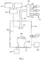
- FIG. 1provides a simple block diagram depicting various semiconductor substrate plasma processing apparatus components arranged for implementing embodiments as disclosed herein.
- a semiconductor substrate plasma processing apparatus 100includes a vacuum chamber 102 that serves to contain plasma in a processing zone, which is generated by a capacitor type system including a showerhead module 104 having an upper RF electrode (not shown) therein working in conjunction with a substrate pedestal module 106 having a lower RF electrode (not shown) therein.
- At least one RF generatoris operable to supply RF energy into a processing zone above an upper surface of a semiconductor substrate 108 in the vacuum chamber 102 to energize process gas supplied into the processing zone of the vacuum chamber 102 into plasma such that a plasma deposition process may be performed in the vacuum chamber 102 .
- a high-frequency RF generator 110 and a low-frequency RF generator 112may each be connected to a matching network 114 , which is connected to the upper RF electrode of the showerhead module 104 such that RF energy may be supplied to the processing zone above the semiconductor substrate 108 in the vacuum chamber 102 .
- the power and frequency of RF energy supplied by matching network 114 to the interior of the vacuum chamber 102is sufficient to generate plasma from the process gas.
- both the high-frequency RF generator 110 and the low-frequency RF generator 112are used, and in an alternate embodiment, just the high-frequency RF generator 110 is used.
- the high-frequency RF generator 110may be operated at frequencies of about 2-100 MHz; in a preferred embodiment at 13.56 MHz or 27 MHz.
- the low-frequency RF generator 112may be operated at about 50 kHz to 2 MHz; in a preferred embodiment at about 350 to 600 kHz.
- the process parametersmay be scaled based on the chamber volume, substrate size, and other factors. Similarly, the flow rates of process gas, may depend on the free volume of the vacuum chamber or processing zone.
- the substrate pedestal module 106supports a semiconductor substrate 108 during processing within the vacuum chamber 102 .
- the substrate pedestal module 106can include a chuck to hold the semiconductor substrate and/or lift pins to raise and lower the semiconductor substrate before, during and/or after the deposition and/or plasma treatment processes.
- the substrate pedestal module 106can include a carrier ring to raise and lower the semiconductor substrate before, during and/or after the deposition and/or plasma treatment processes.
- the chuckmay be an electrostatic chuck, a mechanical chuck, or various other types of chuck as are available for use in the industry and/or research, Details of a lift pin assembly for a substrate pedestal module including an electrostatic chuck can be found in commonly-assigned U.S. Pat. No.
- a backside gas supply 116is operable to supply a heat transfer gas or purge gas through the substrate pedestal module 106 to a region below a lower surface of the semiconductor substrate during processing.
- the substrate pedestal module 106includes the lower RF electrode therein wherein the lower RF electrode is preferably grounded during processing, however in an alternate embodiment, the lower RF electrode may be supplied with RF energy during processing.
- process gasesare introduced from a process gas source 118 into the vacuum chamber 102 via inlet 120 and showerhead module 104 wherein the process gas is formed into plasma with RF energy such that a film may be deposited onto the upper surface of the semiconductor substrate.
- multiple source gas lines 122may be connected to a heated manifold 124 .
- the gasesmay be premixed or supplied separately to the chamber. Appropriate valving and mass flow control mechanisms are employed to ensure that the correct gases are delivered through the showerhead module 104 during semiconductor substrate processing.
- a backside heat transfer gas or purge gasis supplied to a region below a lower surface of the semiconductor substrate supported on the substrate pedestal module 102 .
- the processingis at least one of chemical vapor deposition processing, plasma-enhanced chemical vapor deposition processing, atomic layer deposition processing, plasma-enhanced atomic layer deposition processing, pulsed deposition layer processing, or plasma-enhanced pulsed deposition layer processing.
- a system controller 126is employed to control process conditions during deposition, post deposition treatments, and/or other process operations.
- the controller 126will typically include one or more memory devices and one or more processors.
- the processormay include a CPU or computer, analog and/or digital input/output connections, stepper motor controller boards, etc.
- the controller 126controls all of the activities of the apparatus.
- the system controller 126executes system control software including sets of instructions for controlling the timing of the processing operations, frequency and power of operations of the low-frequency RF generator 112 and the high-frequency RF generator 110 , flow rates and temperatures of precursors and inert gases and their relative mixing, temperature of a semiconductor substrate 108 supported on an upper surface of the substrate pedestal module 106 and a plasma exposed surface of the showerhead module 104 , pressure of the vacuum chamber 102 , and other parameters of a particular process.
- Other computer programs stored on memory devices associated with the controllermay be employed in some embodiments.
- High temperature chuckstypically include a ceramic pedestal and a smaller diameter ceramic stem joined to the underside of the platen. See, for example, commonly-assigned U.S. Patent Publication Nos. 2016/0340781; 2016/0336213; and 2016/0333475, each of which is hereby incorporated by reference in its entirety.
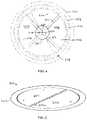
- FIG. 2shows a platen 200 having three co-planar electrodes 202 , 204 , 206 embedded in a ceramic body (not shown).
- Electrode 202is an outer ring-shaped electrode which surrounds D-shaped electrostatic clamping electrodes 204 and 206 .
- a power distribution circuit 208(see FIG. 3 ) is embedded in the ceramic body below the electrodes 202 , 204 , 206 and vertically extending conductive vias 210 connect the outer ring electrode 202 to the power distribution circuit 208 .
- the power distribution circuit 208includes an outer ring 212 underlying the outer ring-shaped electrode 202 and arms 214 extending diagonally across the outer ring 212 .
- the power distribution circuit 208allows power to be fed from a power feed terminal (not shown) located near the center of the underside of the platen.
- the electrostatic clamping electrodes 204 , 206are connected to power feed terminals (not shown) located near the center of the underside of the platen in spaces between the arms 214 of the power distribution circuit 208 .
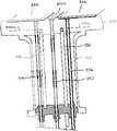
- FIG. 4shows an underside of the platen 200 wherein the arrangement of electrodes 202 , 204 , 206 can be seen along with terminals 216 , 218 , 220 located inside hollow ceramic stem 222 attached to ceramic body 224 .
- Terminal 216is attached to electrostatic clamping electrode 204
- terminal 220is attached to electrostatic clamping electrode 206
- terminal 218is attached to the intersection of arms 214 of power distribution circuit 208 .
- the ceramic body 224includes three through holes 226 sized for passage of lift pins (not shown) for lifting and lowering a wafer onto a support surface of the platen 200 .
- FIG. 5shows an electrostatic chuck comprising platen 300 having an outer ring-shaped electrode 302 surrounding electrostatic clamping electrodes 304 , 306 .
- the outer ring-shaped electrode 302is designed in a way which obviates the need for a power distribution circuit.
- the outer ring-shaped electrode 302includes a radially extending lead (power feed strip) 302 a which extends diagonally across the ring-shaped electrode 302 .
- the lead 302 aallows a terminal (not shown) at a center of the underside of the platen 300 to be electrically connected to the outer ring-shaped electrode 302 .
- the electrostatic chuckis preferably a bipolar chuck with one or more pairs of clamping electrodes having opposed polarities.
- the electrostatic chuckcan include four clamping electrodes separated by feed strips extending diagonally across the outer ring-shaped electrode 302 .
- the feed stripswould be perpendicular and the clamping electrodes would be located inside the four quadrant shaped spaces formed by the outer ring-shaped electrode 302 and the diagonally extending feed strips.
- FIG. 6shows an underside of the platen 300 wherein a hollow ceramic stem 322 is attached to ceramic body 324 .
- Terminal 316is attached to electrostatic clamping electrode 304
- terminal 320is attached to electrostatic clamping electrode 306
- terminal 318is attached to lead 302 a of the ring-shaped outer electrode 302 .
- the ceramic body 324includes three through holes 326 sized for passage of lift pins (not shown) for lifting and lowering a wafer onto a support surface of the platen 300 .
- the platen 300can be used as a high temperature electrostatic chuck of a substrate support module for sequential processing of individual semiconductor wafers wherein the platen 300 is a unitary body made in a single sintering step to provide coplanar electrostatic clamping and RF electrodes and one or more heaters below the coplanar electrodes.
- an embedded power distribution circuit below the RF and electrostatic clamping electrodesincluded power distribution electrode arms which created undesirable inductance effects during wafer processing. By eliminating the power distribution electrode arms, it is possible to eliminate out-of-plane inductors and simplify the manufacturing process by conducting a single sintering step.
- a feed strip 302which extends diagonally across the outer ring-shaped electrode 302 , it is possible to minimize adverse effects of disturbances to the RF field above the wafer being processed.
- the pedestal 300 and stem 322are preferably of ceramic material and a bottom surface of the pedestal 300 can be joined to a flange at an upper end of the stem 322 such as by brazing, friction welding, diffusion bonding, or other suitable technique.
- the interior of the stem 322can include power supply leads, one or more thermocouple leads, and one or more gas supply tubes which supply an inert gas such as argon (Ar) or a heat transfer gas such as helium (He) which is delivered via suitable fluid passages to an underside of a semiconductor substrate located on support surface.
- the power leadscan be one or more feed rods which supply radio-frequency (RF), direct current (DC) and/or alternating current (AC) to electrodes embedded in the pedestal 300 .
- the pedestal 300is preferably a unitary body of sintered ceramic material such as aluminum oxide (alumina), yttria, aluminum nitride, boron nitride, silicon oxide, silicon carbide, silicon nitride, titanium oxide, zirconium oxide, or other suitable material or combination of materials.
- Each electrodepreferably has a planar configuration and is preferably made of an electrically conductive metallic material (e.g., tungsten, molybdenum, tantalum, niobium, cobalt) or electrically conductive non-metallic material (e.g., aluminum oxide-tantalum carbide, aluminum oxide-silicon carbide, aluminum nitride-tungsten, aluminum nitride-tantalum, yttrium oxide-molybdenum).
- the electrodescan be formed from powder materials which are co-fired with the ceramic material of the pedestal.
- the electrodescan be formed of conductive paste which is co-fired with layers of the ceramic material forming the body of the pedestal.
- the pastecan include conductive metal powder of nickel (Ni), tungsten (W), molybdenum (Mo), titanium (Ti), manganese (Mn), copper (Cu), silver (Ag), palladium (Pd), platinum (Pt), rhodium (Rh).
- the electrodescan be formed from a deposited material having a desired electrode pattern or a deposited film which is etched to form a desired electrode pattern. Still yet, the electrodes can comprise preformed grids, plates, wire mesh, or other suitable electrode material and/or configuration.
- the electrodesinclude at least one electrostatic clamping electrode which is powered by a DC power source to provide DC chucking voltage (e.g., about 200 to about 2000 volts), at least one RF electrode powered by a RF power source to provide RF bias voltage (e.g., one or more frequencies of about 400 KHz to about 60 MHz at power levels of about 50 to about 3000 watts) and/or at least one electrode powered by DC and RF power sources via suitable circuitry.
- a DC power sourceto provide DC chucking voltage (e.g., about 200 to about 2000 volts)
- RF bias voltagee.g., one or more frequencies of about 400 KHz to about 60 MHz at power levels of about 50 to about 3000 watts
- DC and RF power sourcesvia suitable circuitry.
- the platencan be made by arranging coplanar electrodes in ceramic material and conducting a single sintering step to embed the electrodes in the sintered ceramic material.
- Examples of techniques for manufacturing ceramic chuckscan be found in commonly-assigned U.S. Pat. Nos. 5,880,922; 6,483,690; and 8,637,194, the disclosures of which are hereby incorporated by reference.
- the outer ring-shaped electrode with integral radially extending lead and the ESC electrodescan be screen printed on a green sheet of aluminum nitride, a green sheet of aluminum nitride or other suitable dielectric material can be placed over the screen printed electrodes, and the resulting compact can be heated pressed and sintered to form the platen. Terminals in holes extending into the underside of the sintered ceramic material can be bonded to each of the electrodes and the stem can be bonded to the underside of the platen.
- FIG. 7illustrates a platen 300 which includes electrically conductive electrodes 304 , 306 such as an electrically conductive grids and feed strip electrode 302 a which is electrically connected to an outer ring-shaped electrode 302 (not shown) embedded therein and a hollow ceramic support stem 322 .
- the platen 300 and stem 322are preferably made of a ceramic material such as aluminum nitride and a bottom surface of the platen 300 is joined to an upper end of the stem 322 such as by brazing, friction welding, diffusion bonding, or other suitable technique.
- a centrally located electrically conductive tube 330is located inside the stem 322 with an upper end of the tube 330 electrically connected to embedded feed strip electrode 302 a .
- An outlet of the tube 330is in fluid communication with a gas passage 342 in an upper surface of the platen 300 .
- the tube 330can be supplied an inert gas such as argon(Ar) or nitrogen (N 2 ) or a heat transfer gas such as helium (He) which is delivered via gas passage 342 to an underside of a semiconductor substrate (not shown) supported on the platen 300 .
- the outer surface of the tube 330can be sealed to the platen 300 by a hermetic seal 332 .
- the inside of the stem 322also houses other components such as electrical feed rods 338 which deliver power to other electrodes such as resistance heaters 340 a , 340 b and additional feed rods 336 which deliver power to electrostatic clamping electrodes 304 , 306 in the platen 300 .
- the rods 336can be hollow for deliver gas through outlets to the underside of a wafer supported on the pedestal 300 .
- the platen 300may cycle between temperatures ranging from about 20° C. to 500° c. and higher.
- the platen 300can have a thickness of up to about 1 inch and a diameter of about 15 inches
- the stem 322can have a diameter of about 3 inches and the distance between the bottom of the stem 322 and the upper surface of the platen 300 can be about 5 inches.
- the tubes 330 , 336can have a diameter of about 4 mm, a length of about 7 to 8 inches.
- the inside of the stem 322accommodates components such as electrical feeds such as palladium/rhodium (Pd/Rh) coated stainless steel or nickel (Ni) rods.
- the feed rods 338can be solid metal rods such as nickel (Ni) rods arranged at circumferentially spaced apart locations inward of an inner surface of the stem 322 , and the two outer electrically conductive feed rods 336 (which can optionally be hollow rods to deliver gas to the upper surface of platen 300 ) are electrically connected to electrostatic clamping electrodes 304 , 306 .
- the solid feed rods 338can supply power to resistance heaters 340 a , 340 b embedded in the platen 300 at a location below the electrostatic clamping electrodes 304 , 306 .
- Electrical connections between the central tube 330 and feed strip 302 a , between the feed rods 336 and the electrodes 304 , 306 , and between the feed rods 338 and the heaters 340 a , 340 bcan include solid terminals/studs/sockets as disclosed in commonly-assigned U.S. Pat. No. 9,088,085, the disclosure of which is hereby incorporated by reference.
- the tube 330 and feed rods 336 , 338can be bonded to the platen 300 and electrodes 302 , 304 , 306 via suitable sintering and/or brazing techniques.
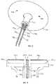
- FIG. 8shows a bottom perspective view of the substrate support pedestal 106 .
- central tube 330 , feed rods 338 and outer tubes 336extend outward from a lower end of the stem 322 .
- FIG. 9is a cross-sectional view of the substrate support pedestal 106 .
- the central tube 330is electrically connected to feed strip electrode 302 a and two feed rods 338 are electrically connected to one or more resistance heaters 340 a , 340 b embedded in the platen 300 at a location below the electrodes 302 , 304 , 306 .
- a pair of feed rods 338can be connected to an inner heater and another pair of feed rods 338 can be connected to an outer heater.
- a single heater or more than two heaterscan be embedded in the platen 300 in any desired geometrical arrangement.
- the central tube 330supplies gas to an outlet 342 in the upper surface of the platen 300 .
Landscapes
- Chemical & Material Sciences (AREA)
- Engineering & Computer Science (AREA)
- Physics & Mathematics (AREA)
- Plasma & Fusion (AREA)
- Analytical Chemistry (AREA)
- General Chemical & Material Sciences (AREA)
- Chemical Kinetics & Catalysis (AREA)
- Materials Engineering (AREA)
- Mechanical Engineering (AREA)
- Metallurgy (AREA)
- Organic Chemistry (AREA)
- General Physics & Mathematics (AREA)
- Condensed Matter Physics & Semiconductors (AREA)
- Manufacturing & Machinery (AREA)
- Computer Hardware Design (AREA)
- Microelectronics & Electronic Packaging (AREA)
- Power Engineering (AREA)
- Container, Conveyance, Adherence, Positioning, Of Wafer (AREA)
- Chemical Vapour Deposition (AREA)
- Physical Vapour Deposition (AREA)
- Gripping On Spindles (AREA)
- Jigs For Machine Tools (AREA)
- Inorganic Insulating Materials (AREA)
- Drying Of Semiconductors (AREA)
Abstract
Description
Claims (20)
Priority Applications (20)
| Application Number | Priority Date | Filing Date | Title |
|---|---|---|---|
| US15/612,423US11289355B2 (en) | 2017-06-02 | 2017-06-02 | Electrostatic chuck for use in semiconductor processing |
| EP23173104.3AEP4258332A3 (en) | 2017-06-02 | 2018-05-30 | Electrostatic chuck for use in semiconductor processing |
| CN201880036474.8ACN110692131B (en) | 2017-06-02 | 2018-05-30 | Electrostatic chucks used in semiconductor processing |
| JP2019566224AJP7271443B2 (en) | 2017-06-02 | 2018-05-30 | Electrostatic chuck for use in semiconductor processing |
| CN202311583318.2ACN117832147A (en) | 2017-06-02 | 2018-05-30 | Electrostatic chuck for use in semiconductor processing |
| EP18809325.6AEP3631846B1 (en) | 2017-06-02 | 2018-05-30 | Electrostatic chuck for use in semiconductor processing |
| KR1020237014797AKR20230065376A (en) | 2017-06-02 | 2018-05-30 | Electrostatic chuck for use in semiconductor processing |
| KR1020207000026AKR20200014881A (en) | 2017-06-02 | 2018-05-30 | Electrostatic chucks for use in semiconductor processing |
| PCT/US2018/034998WO2018222635A1 (en) | 2017-06-02 | 2018-05-30 | Electrostatic chuck for use in semiconductor processing |
| KR1020217033272AKR20210129732A (en) | 2017-06-02 | 2018-05-30 | Electrostatic chuck for use in semiconductor processing |
| KR1020217032163AKR20210124539A (en) | 2017-06-02 | 2018-05-30 | Electrostatic chuck for use in semiconductor processing |
| KR1020217033273AKR20210129733A (en) | 2017-06-02 | 2018-05-30 | Electrostatic chuck for use in semiconductor processing |
| KR1020237033439AKR20230144115A (en) | 2017-06-02 | 2018-05-30 | Electrostatic chuck for use in semiconductor processing |
| TW112143249ATWI865163B (en) | 2017-06-02 | 2018-06-01 | Electrostatic chuck for use in semiconductor processing and method of manufacturing the same |
| TW111140610ATWI826073B (en) | 2017-06-02 | 2018-06-01 | Electrostatic chuck for use in semiconductor processing |
| TW107118835ATWI785055B (en) | 2017-06-02 | 2018-06-01 | Electrostatic chuck for use in semiconductor processing |
| US17/652,243US11817341B2 (en) | 2017-06-02 | 2022-02-23 | Electrostatic chuck for use in semiconductor processing |
| JP2023023008AJP7678832B2 (en) | 2017-06-02 | 2023-02-17 | Electrostatic chuck for use in semiconductor processing - Patent Application 20070123633 |
| US18/481,886US12387965B2 (en) | 2017-06-02 | 2023-10-05 | Electrostatic chuck for use in semiconductor processing |
| JP2025029625AJP2025071338A (en) | 2017-06-02 | 2025-02-27 | Electrostatic chuck for use in semiconductor processing - Patent Application 20070123633 |
Applications Claiming Priority (1)
| Application Number | Priority Date | Filing Date | Title |
|---|---|---|---|
| US15/612,423US11289355B2 (en) | 2017-06-02 | 2017-06-02 | Electrostatic chuck for use in semiconductor processing |
Related Child Applications (1)
| Application Number | Title | Priority Date | Filing Date |
|---|---|---|---|
| US17/652,243ContinuationUS11817341B2 (en) | 2017-06-02 | 2022-02-23 | Electrostatic chuck for use in semiconductor processing |
Publications (2)
| Publication Number | Publication Date |
|---|---|
| US20180350649A1 US20180350649A1 (en) | 2018-12-06 |
| US11289355B2true US11289355B2 (en) | 2022-03-29 |
Family
ID=64456121
Family Applications (3)
| Application Number | Title | Priority Date | Filing Date |
|---|---|---|---|
| US15/612,423Active2038-09-09US11289355B2 (en) | 2017-06-02 | 2017-06-02 | Electrostatic chuck for use in semiconductor processing |
| US17/652,243ActiveUS11817341B2 (en) | 2017-06-02 | 2022-02-23 | Electrostatic chuck for use in semiconductor processing |
| US18/481,886ActiveUS12387965B2 (en) | 2017-06-02 | 2023-10-05 | Electrostatic chuck for use in semiconductor processing |
Family Applications After (2)
| Application Number | Title | Priority Date | Filing Date |
|---|---|---|---|
| US17/652,243ActiveUS11817341B2 (en) | 2017-06-02 | 2022-02-23 | Electrostatic chuck for use in semiconductor processing |
| US18/481,886ActiveUS12387965B2 (en) | 2017-06-02 | 2023-10-05 | Electrostatic chuck for use in semiconductor processing |
Country Status (7)
| Country | Link |
|---|---|
| US (3) | US11289355B2 (en) |
| EP (2) | EP4258332A3 (en) |
| JP (3) | JP7271443B2 (en) |
| KR (6) | KR20200014881A (en) |
| CN (2) | CN110692131B (en) |
| TW (3) | TWI826073B (en) |
| WO (1) | WO2018222635A1 (en) |
Cited By (5)
| Publication number | Priority date | Publication date | Assignee | Title |
|---|---|---|---|---|
| US20220181184A1 (en)* | 2017-06-02 | 2022-06-09 | Lam Research Corporation | Electrostatic chuck for use in semiconductor processing |
| US11835868B2 (en) | 2018-03-20 | 2023-12-05 | Lam Research Corporation | Protective coating for electrostatic chucks |
| US11990360B2 (en) | 2018-01-31 | 2024-05-21 | Lam Research Corporation | Electrostatic chuck (ESC) pedestal voltage isolation |
| US12217939B2 (en) | 2018-08-02 | 2025-02-04 | Lam Research Corporation | RF tuning systems including tuning circuits having impedances for setting and adjusting parameters of electrodes in electrostatic chucks |
| US12243725B2 (en) | 2017-09-05 | 2025-03-04 | Lam Research Corporation | High temperature RF connection with integral thermal choke |
Families Citing this family (37)
| Publication number | Priority date | Publication date | Assignee | Title |
|---|---|---|---|---|
| US10510575B2 (en) | 2017-09-20 | 2019-12-17 | Applied Materials, Inc. | Substrate support with multiple embedded electrodes |
| US11664206B2 (en) | 2017-11-08 | 2023-05-30 | Taiwan Semiconductor Manufacturing Co., Ltd. | Arcing protection method and processing tool |
| US10555412B2 (en) | 2018-05-10 | 2020-02-04 | Applied Materials, Inc. | Method of controlling ion energy distribution using a pulse generator with a current-return output stage |
| JP7145042B2 (en)* | 2018-11-08 | 2022-09-30 | 東京エレクトロン株式会社 | Substrate support and plasma processing equipment |
| US11476145B2 (en) | 2018-11-20 | 2022-10-18 | Applied Materials, Inc. | Automatic ESC bias compensation when using pulsed DC bias |
| WO2020117371A1 (en)* | 2018-12-07 | 2020-06-11 | Applied Materials, Inc. | Ground electrode formed in an electrostatic chuck for a plasma processing chamber |
| KR102827481B1 (en) | 2019-01-22 | 2025-06-30 | 어플라이드 머티어리얼스, 인코포레이티드 | Feedback loop to control pulse voltage waveform |
| US11508554B2 (en) | 2019-01-24 | 2022-11-22 | Applied Materials, Inc. | High voltage filter assembly |
| KR102628919B1 (en)* | 2019-05-29 | 2024-01-24 | 주식회사 원익아이피에스 | Substrate processing apparatus and method using the same |
| US20210159107A1 (en)* | 2019-11-21 | 2021-05-27 | Applied Materials, Inc. | Edge uniformity tunability on bipolar electrostatic chuck |
| US11984298B2 (en) | 2019-12-02 | 2024-05-14 | Lam Research Corporation | Impedance transformation in radio-frequency-assisted plasma generation |
| US11848176B2 (en) | 2020-07-31 | 2023-12-19 | Applied Materials, Inc. | Plasma processing using pulsed-voltage and radio-frequency power |
| KR20230078792A (en)* | 2020-10-01 | 2023-06-02 | 램 리써치 코포레이션 | High temperature pedestal with extended electrostatic chuck electrode |
| US11798790B2 (en) | 2020-11-16 | 2023-10-24 | Applied Materials, Inc. | Apparatus and methods for controlling ion energy distribution |
| US11901157B2 (en) | 2020-11-16 | 2024-02-13 | Applied Materials, Inc. | Apparatus and methods for controlling ion energy distribution |
| CN112768401B (en)* | 2021-02-01 | 2025-06-17 | 杭州晶通科技有限公司 | An electrostatic adsorption chuck |
| US11495470B1 (en) | 2021-04-16 | 2022-11-08 | Applied Materials, Inc. | Method of enhancing etching selectivity using a pulsed plasma |
| US11851761B2 (en)* | 2021-04-16 | 2023-12-26 | Taiwan Semiconductor Manufacturing Company, Ltd. | Semiconductor processing tool |
| US11791138B2 (en) | 2021-05-12 | 2023-10-17 | Applied Materials, Inc. | Automatic electrostatic chuck bias compensation during plasma processing |
| US11948780B2 (en) | 2021-05-12 | 2024-04-02 | Applied Materials, Inc. | Automatic electrostatic chuck bias compensation during plasma processing |
| US11967483B2 (en) | 2021-06-02 | 2024-04-23 | Applied Materials, Inc. | Plasma excitation with ion energy control |
| US20220399185A1 (en) | 2021-06-09 | 2022-12-15 | Applied Materials, Inc. | Plasma chamber and chamber component cleaning methods |
| US12394596B2 (en) | 2021-06-09 | 2025-08-19 | Applied Materials, Inc. | Plasma uniformity control in pulsed DC plasma chamber |
| US11810760B2 (en) | 2021-06-16 | 2023-11-07 | Applied Materials, Inc. | Apparatus and method of ion current compensation |
| US11569066B2 (en) | 2021-06-23 | 2023-01-31 | Applied Materials, Inc. | Pulsed voltage source for plasma processing applications |
| US11476090B1 (en) | 2021-08-24 | 2022-10-18 | Applied Materials, Inc. | Voltage pulse time-domain multiplexing |
| US12106938B2 (en) | 2021-09-14 | 2024-10-01 | Applied Materials, Inc. | Distortion current mitigation in a radio frequency plasma processing chamber |
| KR20240137100A (en)* | 2022-01-31 | 2024-09-19 | 램 리써치 코포레이션 | Method and device for designing a radio frequency grid to reduce membrane asymmetry in ESC |
| US12233501B2 (en) | 2022-02-17 | 2025-02-25 | Tes Co., Ltd | Substrate support device |
| KR20230123876A (en) | 2022-02-17 | 2023-08-24 | 주식회사 테스 | A substrate support device |
| US20230282506A1 (en)* | 2022-03-02 | 2023-09-07 | Applied Materials, Inc. | Biasable rotating pedestal |
| US11972924B2 (en) | 2022-06-08 | 2024-04-30 | Applied Materials, Inc. | Pulsed voltage source for plasma processing applications |
| US12315732B2 (en) | 2022-06-10 | 2025-05-27 | Applied Materials, Inc. | Method and apparatus for etching a semiconductor substrate in a plasma etch chamber |
| US12272524B2 (en) | 2022-09-19 | 2025-04-08 | Applied Materials, Inc. | Wideband variable impedance load for high volume manufacturing qualification and on-site diagnostics |
| US12111341B2 (en) | 2022-10-05 | 2024-10-08 | Applied Materials, Inc. | In-situ electric field detection method and apparatus |
| CN120359590A (en)* | 2022-12-16 | 2025-07-22 | 朗姆研究公司 | Method and apparatus for biasing an electrostatic chuck |
| US20250299983A1 (en)* | 2024-03-19 | 2025-09-25 | Tokyo Electron Limited | Ceramic heater assembly with internal and external heating functionality useful in the fabrication of microelectronic devices |
Citations (58)
| Publication number | Priority date | Publication date | Assignee | Title |
|---|---|---|---|---|
| US4384918A (en) | 1980-09-30 | 1983-05-24 | Fujitsu Limited | Method and apparatus for dry etching and electrostatic chucking device used therein |
| US4692836A (en)* | 1983-10-31 | 1987-09-08 | Toshiba Kikai Kabushiki Kaisha | Electrostatic chucks |
| JPS63278322A (en) | 1987-05-11 | 1988-11-16 | Fujitsu Ltd | Vapor phase growth equipment |
| JPH06260430A (en) | 1993-03-08 | 1994-09-16 | Eiko:Kk | Plate heater and manufacturing method thereof |
| JPH0778766A (en) | 1993-06-24 | 1995-03-20 | Tokyo Electron Ltd | Gas treating device |
| US5668331A (en) | 1995-08-18 | 1997-09-16 | U.S. Philips Corporation | Position sensor |
| JPH10326788A (en) | 1997-05-26 | 1998-12-08 | Kokusai Electric Co Ltd | Heater unit and substrate processing device |
| US5880922A (en) | 1995-03-10 | 1999-03-09 | Lam Research Corporation | Multilayered electrostatic chuck and method of manufacture thereof |
| US6104596A (en) | 1998-04-21 | 2000-08-15 | Applied Materials, Inc. | Apparatus for retaining a subtrate in a semiconductor wafer processing system and a method of fabricating same |
| US6156686A (en) | 1997-12-10 | 2000-12-05 | Ngk Insulators, Ltd. | Porous composite ceramic sintered bodies and a production process thereof |
| US20010019472A1 (en) | 1996-09-19 | 2001-09-06 | Seiichiro Kanno | Electrostatic chuck, and method of and apparatus for processing sample using the chuck |
| US20010027972A1 (en)* | 2000-02-03 | 2001-10-11 | Ngk Insulators,Ltd. | Heating apparatus |
| US6303879B1 (en) | 1997-04-01 | 2001-10-16 | Applied Materials, Inc. | Laminated ceramic with multilayer electrodes and method of fabrication |
| US20020027762A1 (en) | 1998-09-29 | 2002-03-07 | Shinji Yamaguchi | Electrostatic chuck |
| US6483690B1 (en) | 2001-06-28 | 2002-11-19 | Lam Research Corporation | Ceramic electrostatic chuck assembly and method of making |
| JP2004356624A (en) | 2003-05-07 | 2004-12-16 | Tokyo Electron Ltd | Mounting stand structure and heat treatment equipment |
| US6860965B1 (en) | 2000-06-23 | 2005-03-01 | Novellus Systems, Inc. | High throughput architecture for semiconductor processing |
| US20050045618A1 (en) | 2001-07-09 | 2005-03-03 | Ibiden Co., Ltd. | Ceramic heater and ceramic joined article |
| JP2005063991A (en) | 2003-08-08 | 2005-03-10 | Sumitomo Electric Ind Ltd | Semiconductor manufacturing equipment |
| US20050215415A1 (en) | 2004-03-29 | 2005-09-29 | Ngk Insulators, Ltd. | Aluminum nitride substrate and production method |
| US20050213279A1 (en)* | 2004-03-26 | 2005-09-29 | Hirofumi Hayakawa | Electrostatic chuck and substrate fixing method using the same |
| US6964812B2 (en) | 1999-09-06 | 2005-11-15 | Ibiden Co., Ltd. | Carbon-containing aluminum nitride sintered compact and ceramic substrate for use in equipment for manufacturing or inspecting semiconductor |
| US20050258160A1 (en) | 2004-04-12 | 2005-11-24 | Ngk Insulators, Ltd. | Substrate heating device |
| US20060011611A1 (en)* | 2004-06-28 | 2006-01-19 | Ngk Insulators, Ltd. | Substrate heating apparatus |
| JP2006295138A (en) | 2005-03-16 | 2006-10-26 | Tokyo Electron Ltd | Substrate mounting mechanism and substrate processing apparatus having substrate heating function |
| US20070042897A1 (en) | 2005-08-19 | 2007-02-22 | Ngk Insulators, Ltd. | Yttria sintered body, electrostatic chuck, and manufacturing method of yttria sintered body |
| WO2007055381A1 (en) | 2005-11-14 | 2007-05-18 | Tokyo Electron Limited | Film forming apparatus and placing table for film forming apparatus |
| US20070223173A1 (en)* | 2004-03-19 | 2007-09-27 | Hiroshi Fujisawa | Bipolar Electrostatic Chuck |
| US20080062609A1 (en)* | 2006-08-10 | 2008-03-13 | Shinji Himori | Electrostatic chuck device |
| US20090274590A1 (en) | 2008-05-05 | 2009-11-05 | Applied Materials, Inc. | Plasma reactor electrostatic chuck having a coaxial rf feed and multizone ac heater power transmission through the coaxial feed |
| US20090283933A1 (en) | 2005-03-25 | 2009-11-19 | Ngk Insulators, Ltd. | Ceramic member and method for producing the same |
| US7701693B2 (en) | 2006-09-13 | 2010-04-20 | Ngk Insulators, Ltd. | Electrostatic chuck with heater and manufacturing method thereof |
| US20110031217A1 (en)* | 2009-08-04 | 2011-02-10 | Tokyo Electron Limited | Plasma processing apparatus and plasma processing method |
| US20110096461A1 (en) | 2009-10-26 | 2011-04-28 | Shinko Electric Industries Co., Ltd. | Substrate for electrostatic chuck and electrostatic chuck |
| US20120006493A1 (en) | 2006-08-08 | 2012-01-12 | White John M | Heating and cooling of substrate support |
| US8136820B2 (en) | 2006-08-22 | 2012-03-20 | Ngk Insulators, Ltd. | Electrostatic chuck with heater and manufacturing method thereof |
| JP2012089694A (en) | 2010-10-20 | 2012-05-10 | Sumitomo Electric Ind Ltd | Wafer holder of 2 layer rf structure |
| US20120164834A1 (en)* | 2010-12-22 | 2012-06-28 | Kevin Jennings | Variable-Density Plasma Processing of Semiconductor Substrates |
| US20130001899A1 (en) | 2011-07-01 | 2013-01-03 | Applied Materials, Inc. | Electrostatic chuck assembly |
| US20130220988A1 (en) | 2010-10-25 | 2013-08-29 | Ngk Insulators, Ltd. | Heating device |
| US20130284374A1 (en) | 2012-04-26 | 2013-10-31 | Dmitry Lubomirsky | High temperature electrostatic chuck with real-time heat zone regulating capability |
| US8637194B2 (en) | 2008-09-02 | 2014-01-28 | Bio-Nano Power, Llc | Bio-nano power cells and their uses |
| US20140117119A1 (en) | 2012-10-26 | 2014-05-01 | Ngk Insulators, Ltd. | Member for semiconductor manufacturing apparatus and method for manufacturing the same |
| US8840754B2 (en) | 2010-09-17 | 2014-09-23 | Lam Research Corporation | Polar regions for electrostatic de-chucking with lift pins |
| US20140340813A1 (en) | 2011-09-30 | 2014-11-20 | Toto Ltd. | Ac-driven electrostatic chuck |
| US8981263B2 (en) | 2009-12-10 | 2015-03-17 | Tokyo Electron Limited | Electrostatic chuck apparatus |
| US9017484B2 (en) | 2012-11-06 | 2015-04-28 | Ngk Insulators, Ltd. | Susceptor |
| US20150116889A1 (en) | 2012-05-07 | 2015-04-30 | Tocalo Co., Ltd. | Electrostatic chuck and method of manufacturing electrostatic chuck |
| US20160002779A1 (en)* | 2014-07-02 | 2016-01-07 | Applied Materials, Inc. | Multi-zone pedestal for plasma processing |
| US20160148828A1 (en) | 2014-11-21 | 2016-05-26 | Varian Semiconductor Equipment Associates, Inc. | Detachable high-temperature electrostatic chuck assembly |
| US9418884B2 (en) | 2013-05-09 | 2016-08-16 | Shinko Electric Industries Co., Ltd. | Electrostatic chuck and semiconductor manufacturing device |
| US20160336213A1 (en) | 2015-05-12 | 2016-11-17 | Lam Research Corporation | High temperature substrate pedestal module and components thereof |
| US20160333475A1 (en) | 2015-05-12 | 2016-11-17 | Lam Research Corporation | Substrate pedestal module including backside gas delivery tube and method of making |
| US20160340781A1 (en) | 2015-05-22 | 2016-11-24 | Lam Research Corporation | Deposition apparatus including edge plenum showerhead assembly |
| US10147610B1 (en)* | 2017-05-30 | 2018-12-04 | Lam Research Corporation | Substrate pedestal module including metallized ceramic tubes for RF and gas delivery |
| US20180350568A1 (en)* | 2017-05-30 | 2018-12-06 | Tokyo Electron Limited | Method of operating electrostatic chuck of plasma processing apparatus |
| US20190355556A1 (en)* | 2017-03-06 | 2019-11-21 | Ngk Insulators, Ltd. | Wafer support table |
| CN110692131A (en) | 2017-06-02 | 2020-01-14 | 朗姆研究公司 | Electrostatic chucks for semiconductor processing |
Family Cites Families (203)
| Publication number | Priority date | Publication date | Assignee | Title |
|---|---|---|---|---|
| US2491167A (en) | 1946-03-19 | 1949-12-13 | Charles E Drew | Collet chuck |
| US2684698A (en) | 1950-06-01 | 1954-07-27 | Keller Tool Co | Tool for running threaded fastening elements |
| US3895832A (en) | 1974-05-13 | 1975-07-22 | Mueller Co | Collet compression connection |
| US4552430A (en) | 1982-09-30 | 1985-11-12 | Myers Electric Products, Inc. | Connector head for electric terminal box |
| US4657616A (en) | 1985-05-17 | 1987-04-14 | Benzing Technologies, Inc. | In-situ CVD chamber cleaner |
| US4897853A (en) | 1988-06-01 | 1990-01-30 | King, Taudevin & Gregson (Holdings)Limited | Refractory ceramic electrode |
| JPH04236449A (en) | 1991-01-21 | 1992-08-25 | Fuji Electric Co Ltd | Electrostatic chuck |
| JPH06326175A (en) | 1993-04-22 | 1994-11-25 | Applied Materials Inc | Wafer support used in integrated circuit processing equipment protective coating on dielectric material and method of forming the same |
| JPH07169737A (en)* | 1993-12-14 | 1995-07-04 | Tokyo Electron Ltd | Treating device |
| JPH07201496A (en) | 1993-12-29 | 1995-08-04 | Matsushita Electric Ind Co Ltd | Plasma generating method and plasma generating apparatus |
| US5463526A (en) | 1994-01-21 | 1995-10-31 | Lam Research Corporation | Hybrid electrostatic chuck |
| US5507874A (en) | 1994-06-03 | 1996-04-16 | Applied Materials, Inc. | Method of cleaning of an electrostatic chuck in plasma reactors |
| JP3249696B2 (en) | 1994-11-28 | 2002-01-21 | 日新電機株式会社 | Electrostatic chuck and method of using the same |
| US6042686A (en) | 1995-06-30 | 2000-03-28 | Lam Research Corporation | Power segmented electrode |
| US5633073A (en) | 1995-07-14 | 1997-05-27 | Applied Materials, Inc. | Ceramic susceptor with embedded metal electrode and eutectic connection |
| JP3949186B2 (en) | 1995-12-25 | 2007-07-25 | 富士通株式会社 | Substrate mounting table, plasma processing apparatus, and semiconductor device manufacturing method |
| JP3847363B2 (en) | 1996-02-02 | 2006-11-22 | 富士通株式会社 | Semiconductor wafer processing apparatus and semiconductor wafer processing method |
| US5812362A (en) | 1996-06-14 | 1998-09-22 | Applied Materials, Inc. | Method and apparatus for the use of diamond films as dielectric coatings on electrostatic chucks |
| US5829791A (en) | 1996-09-20 | 1998-11-03 | Bruker Instruments, Inc. | Insulated double bayonet coupler for fluid recirculation apparatus |
| US6066836A (en) | 1996-09-23 | 2000-05-23 | Applied Materials, Inc. | High temperature resistive heater for a process chamber |
| US6616767B2 (en) | 1997-02-12 | 2003-09-09 | Applied Materials, Inc. | High temperature ceramic heater assembly with RF capability |
| US5737178A (en) | 1997-03-06 | 1998-04-07 | Applied Materials, Inc. | Monocrystalline ceramic coating having integral bonding interconnects for electrostatic chucks |
| TW422892B (en) | 1997-03-27 | 2001-02-21 | Applied Materials Inc | Technique for improving chucking reproducibility |
| JP3624628B2 (en) | 1997-05-20 | 2005-03-02 | 東京エレクトロン株式会社 | Film forming method and film forming apparatus |
| US5841624A (en) | 1997-06-09 | 1998-11-24 | Applied Materials, Inc. | Cover layer for a substrate support chuck and method of fabricating same |
| US6936153B1 (en) | 1997-09-30 | 2005-08-30 | Semitool, Inc. | Semiconductor plating system workpiece support having workpiece-engaging electrode with pre-conditioned contact face |
| US6081414A (en) | 1998-05-01 | 2000-06-27 | Applied Materials, Inc. | Apparatus for improved biasing and retaining of a workpiece in a workpiece processing system |
| US6072685A (en) | 1998-05-22 | 2000-06-06 | Applied Materials, Inc. | Electrostatic chuck having an electrical connector with housing |
| US6221221B1 (en) | 1998-11-16 | 2001-04-24 | Applied Materials, Inc. | Apparatus for providing RF return current path control in a semiconductor wafer processing system |
| US6151203A (en) | 1998-12-14 | 2000-11-21 | Applied Materials, Inc. | Connectors for an electrostatic chuck and combination thereof |
| US6213478B1 (en) | 1999-03-11 | 2001-04-10 | Moore Epitaxial, Inc. | Holding mechanism for a susceptor in a substrate processing reactor |
| US6466881B1 (en) | 1999-04-22 | 2002-10-15 | Applied Materials Inc. | Method for monitoring the quality of a protective coating in a reactor chamber |
| US6261977B1 (en) | 1999-09-08 | 2001-07-17 | United Microelectronics Corp. | Method for preventing an electrostatic chuck from being corroded during a cleaning process |
| JP3914671B2 (en) | 1999-11-30 | 2007-05-16 | 京セラ株式会社 | Wafer support member |
| JP4637316B2 (en) | 2000-02-24 | 2011-02-23 | 京セラ株式会社 | Ceramic heater having cylindrical body and heating device using the same |
| US6592709B1 (en) | 2000-04-05 | 2003-07-15 | Applied Materials Inc. | Method and apparatus for plasma processing |
| JP4398064B2 (en) | 2000-05-12 | 2010-01-13 | 日本発條株式会社 | Heating device |
| US7288491B2 (en) | 2000-08-11 | 2007-10-30 | Applied Materials, Inc. | Plasma immersion ion implantation process |
| US7465478B2 (en) | 2000-08-11 | 2008-12-16 | Applied Materials, Inc. | Plasma immersion ion implantation process |
| US6403491B1 (en) | 2000-11-01 | 2002-06-11 | Applied Materials, Inc. | Etch method using a dielectric etch chamber with expanded process window |
| JP3870824B2 (en) | 2001-09-11 | 2007-01-24 | 住友電気工業株式会社 | SUBSTRATE HOLDER, SENSOR FOR SEMICONDUCTOR MANUFACTURING DEVICE, AND PROCESSING DEVICE |
| JP2003124296A (en)* | 2001-10-17 | 2003-04-25 | Sumitomo Osaka Cement Co Ltd | Susceptor and its manufacturing method |
| US6879051B1 (en) | 2002-01-16 | 2005-04-12 | Advanced Micro Devices, Inc. | Systems and methods to determine seed layer thickness of trench sidewalls |
| KR100511854B1 (en)* | 2002-06-18 | 2005-09-02 | 아네르바 가부시키가이샤 | Electrostatic chuck device |
| JP4034145B2 (en) | 2002-08-09 | 2008-01-16 | 住友大阪セメント株式会社 | Susceptor device |
| JP3962661B2 (en) | 2002-08-30 | 2007-08-22 | 三菱重工業株式会社 | Electrostatic chuck support mechanism, support base device, and plasma processing apparatus |
| EP1408140A1 (en) | 2002-10-11 | 2004-04-14 | STMicroelectronics S.r.l. | A high-density plasma process for depositing a layer of Silicon Nitride |
| US7270761B2 (en) | 2002-10-18 | 2007-09-18 | Appleid Materials, Inc | Fluorine free integrated process for etching aluminum including chamber dry clean |
| CN100388434C (en) | 2003-03-12 | 2008-05-14 | 东京毅力科创株式会社 | Substrate holding structure and plasma processing apparatus for semiconductor processing |
| JP4347295B2 (en) | 2003-04-18 | 2009-10-21 | 株式会社日立国際電気 | Semiconductor manufacturing apparatus and semiconductor device manufacturing method |
| CN1310285C (en) | 2003-05-12 | 2007-04-11 | 东京毅力科创株式会社 | Processing device |
| US7567421B2 (en) | 2003-06-17 | 2009-07-28 | Creative Technology Corporation | Bipolar electrostatic chuck |
| JP2005007699A (en) | 2003-06-18 | 2005-01-13 | Konica Minolta Photo Imaging Inc | Inkjet recording material and method for recording using it |
| JP2005018992A (en) | 2003-06-23 | 2005-01-20 | Ibiden Co Ltd | Electrode embedding member for plasma generator |
| JP2005072286A (en) | 2003-08-25 | 2005-03-17 | Kyocera Corp | Electrostatic chuck |
| TWI236055B (en) | 2003-09-05 | 2005-07-11 | United Microelectronics Corp | Plasma apparatus and method capable of adaptive impedance matching |
| JP4411100B2 (en) | 2004-02-18 | 2010-02-10 | キヤノン株式会社 | Exposure equipment |
| US7824498B2 (en) | 2004-02-24 | 2010-11-02 | Applied Materials, Inc. | Coating for reducing contamination of substrates during processing |
| JP2005347620A (en) | 2004-06-04 | 2005-12-15 | Tokyo Electron Ltd | Plasma treatment apparatus and placement base unit thereof |
| US20050274324A1 (en) | 2004-06-04 | 2005-12-15 | Tokyo Electron Limited | Plasma processing apparatus and mounting unit thereof |
| US7375946B2 (en) | 2004-08-16 | 2008-05-20 | Applied Materials, Inc. | Method and apparatus for dechucking a substrate |
| JP4386360B2 (en) | 2004-12-06 | 2009-12-16 | 信越化学工業株式会社 | Electrostatic chuck |
| US7430986B2 (en) | 2005-03-18 | 2008-10-07 | Lam Research Corporation | Plasma confinement ring assemblies having reduced polymer deposition characteristics |
| JP2006302887A (en) | 2005-04-20 | 2006-11-02 | Ngk Insulators Ltd | Power supply member and heating device |
| JP4672597B2 (en) | 2005-06-02 | 2011-04-20 | 日本碍子株式会社 | Substrate processing equipment |
| US9520276B2 (en) | 2005-06-22 | 2016-12-13 | Tokyo Electron Limited | Electrode assembly and plasma processing apparatus |
| US7683289B2 (en) | 2005-12-16 | 2010-03-23 | Lam Research Corporation | Apparatus and method for controlling plasma density profile |
| JP5254533B2 (en) | 2006-03-31 | 2013-08-07 | 東京エレクトロン株式会社 | Plasma processing apparatus and method |
| JP4381393B2 (en) | 2006-04-28 | 2009-12-09 | 信越化学工業株式会社 | Electrostatic chuck |
| US8440049B2 (en) | 2006-05-03 | 2013-05-14 | Applied Materials, Inc. | Apparatus for etching high aspect ratio features |
| US20080009417A1 (en) | 2006-07-05 | 2008-01-10 | General Electric Company | Coating composition, article, and associated method |
| US20080029032A1 (en) | 2006-08-01 | 2008-02-07 | Sun Jennifer Y | Substrate support with protective layer for plasma resistance |
| US7619870B2 (en) | 2006-08-10 | 2009-11-17 | Tokyo Electron Limited | Electrostatic chuck |
| CN200956667Y (en) | 2006-09-26 | 2007-10-03 | 李生 | Electric-heating radiation tube with ceramic coating on inner wall |
| US7589950B2 (en)* | 2006-10-13 | 2009-09-15 | Applied Materials, Inc. | Detachable electrostatic chuck having sealing assembly |
| JP4768699B2 (en) | 2006-11-30 | 2011-09-07 | キヤノンアネルバ株式会社 | Power introduction apparatus and film forming method |
| US20080167720A1 (en) | 2007-01-08 | 2008-07-10 | Warsaw Orthopedic, Inc. | Expandable vertebral body replacement device |
| JP4903610B2 (en) | 2007-03-27 | 2012-03-28 | 東京エレクトロン株式会社 | Plasma processing equipment |
| US8294069B2 (en) | 2007-03-28 | 2012-10-23 | Ngk Insulators, Ltd. | Heating device for heating a wafer |
| JP5660753B2 (en)* | 2007-07-13 | 2015-01-28 | アプライド マテリアルズ インコーポレイテッドApplied Materials,Incorporated | High temperature cathode for plasma etching |
| US7625227B1 (en) | 2007-07-31 | 2009-12-01 | Agilent Technologies, Inc. | High performance blind-mate connector |
| JP2009123929A (en) | 2007-11-15 | 2009-06-04 | Tokyo Electron Ltd | Plasma treatment apparatus |
| KR101415551B1 (en)* | 2008-01-25 | 2014-07-04 | (주)소슬 | Electrostatic chuck, method of manufacturing the same and apparatus for processing a substrate including the same |
| US7968439B2 (en) | 2008-02-06 | 2011-06-28 | Applied Materials, Inc. | Plasma immersion ion implantation method using a pure or nearly pure silicon seasoning layer on the chamber interior surfaces |
| JP4450106B1 (en) | 2008-03-11 | 2010-04-14 | 東京エレクトロン株式会社 | Mounting table structure and processing device |
| US8540819B2 (en) | 2008-03-21 | 2013-09-24 | Ngk Insulators, Ltd. | Ceramic heater |
| TWI475594B (en) | 2008-05-19 | 2015-03-01 | Entegris Inc | Electrostatic chuck |
| US7702077B2 (en) | 2008-05-19 | 2010-04-20 | General Electric Company | Apparatus for a compact HV insulator for x-ray and vacuum tube and method of assembling same |
| CN102077338A (en) | 2008-06-24 | 2011-05-25 | 应用材料股份有限公司 | Pedestal heater for low temperature pecvd application |
| KR101582785B1 (en) | 2008-08-12 | 2016-01-07 | 어플라이드 머티어리얼스, 인코포레이티드 | Electrostatic chuck assembly |
| US20100104852A1 (en) | 2008-10-23 | 2010-04-29 | Molecular Imprints, Inc. | Fabrication of High-Throughput Nano-Imprint Lithography Templates |
| WO2010087385A1 (en) | 2009-01-29 | 2010-08-05 | 東京エレクトロン株式会社 | Film deposition device and gas ejection member |
| JP5657262B2 (en) | 2009-03-27 | 2015-01-21 | 東京エレクトロン株式会社 | Plasma processing equipment |
| WO2010132640A2 (en) | 2009-05-15 | 2010-11-18 | Entegris, Inc. | Electrostatic chuck with polymer protrusions |
| TW201100578A (en) | 2009-06-19 | 2011-01-01 | Saint Gobain Ceramics & Plastics Inc | Sealed plasma coatings |
| US9213021B2 (en) | 2009-07-16 | 2015-12-15 | Waters Technologies Corporation | Self-unlocking fluid-tight connector |
| JP5460184B2 (en) | 2009-08-28 | 2014-04-02 | 株式会社日本セラテック | Support device |
| JP2011061040A (en) | 2009-09-10 | 2011-03-24 | Tokyo Electron Ltd | Stage structure and processing apparatus |
| JP2011165891A (en) | 2010-02-09 | 2011-08-25 | Tokyo Electron Ltd | Mounting stand structure, and processing device |
| JP5218865B2 (en)* | 2010-03-26 | 2013-06-26 | Toto株式会社 | Electrostatic chuck |
| KR101731136B1 (en) | 2010-05-28 | 2017-04-27 | 엔테그리스, 아이엔씨. | High surface resistivity electrostatic chuck |
| WO2012018875A1 (en) | 2010-08-06 | 2012-02-09 | American Grease Stick Company | Hand held flaring tool |
| CN103222043B (en) | 2010-09-08 | 2016-10-12 | 恩特格林斯公司 | A kind of high conductivity electrostatic chuck |
| US9399812B2 (en) | 2011-10-11 | 2016-07-26 | Applied Materials, Inc. | Methods of preventing plasma induced damage during substrate processing |
| US8884524B2 (en) | 2011-11-22 | 2014-11-11 | Applied Materials, Inc. | Apparatus and methods for improving reliability of RF grounding |
| US20170004925A1 (en) | 2012-02-03 | 2017-01-05 | Comet Ag | Power delivery systems and manufacturing equipment including a variable vacuum capacitor |
| JP5351316B1 (en) | 2012-08-15 | 2013-11-27 | 株式会社アドバンテスト | Sample holder and electron beam exposure method using the same |
| JP5996340B2 (en) | 2012-09-07 | 2016-09-21 | 東京エレクトロン株式会社 | Plasma etching equipment |
| US9088085B2 (en) | 2012-09-21 | 2015-07-21 | Novellus Systems, Inc. | High temperature electrode connections |
| JP6207880B2 (en) | 2012-09-26 | 2017-10-04 | 東芝メモリ株式会社 | Plasma processing apparatus and plasma processing method |
| JPWO2014057771A1 (en) | 2012-10-12 | 2016-09-05 | 株式会社日立金属ネオマテリアル | Metal substrate |
| CN103794445B (en) | 2012-10-29 | 2016-03-16 | 中微半导体设备(上海)有限公司 | For electrostatic chuck assembly and the manufacture method of plasma process chamber |
| JP6001675B2 (en) | 2012-11-28 | 2016-10-05 | 京セラ株式会社 | Mounting member and manufacturing method thereof |
| US10100908B2 (en) | 2012-11-30 | 2018-10-16 | Kuroda Precision Industries Ltd. | Shaft end adapter and ball screw assembly |
| US9916998B2 (en) | 2012-12-04 | 2018-03-13 | Applied Materials, Inc. | Substrate support assembly having a plasma resistant protective layer |
| US9685356B2 (en) | 2012-12-11 | 2017-06-20 | Applied Materials, Inc. | Substrate support assembly having metal bonded protective layer |
| US8941969B2 (en) | 2012-12-21 | 2015-01-27 | Applied Materials, Inc. | Single-body electrostatic chuck |
| KR101333631B1 (en) | 2012-12-21 | 2013-11-27 | (주)보부하이테크 | Quartz heater |
| US9358702B2 (en) | 2013-01-18 | 2016-06-07 | Applied Materials, Inc. | Temperature management of aluminium nitride electrostatic chuck |
| US9666466B2 (en) | 2013-05-07 | 2017-05-30 | Applied Materials, Inc. | Electrostatic chuck having thermally isolated zones with minimal crosstalk |
| US8934826B2 (en) | 2013-05-30 | 2015-01-13 | Xerox Corporation | Surface tension interference coating process for precise feature control |
| JP6119430B2 (en) | 2013-05-31 | 2017-04-26 | 住友大阪セメント株式会社 | Electrostatic chuck device |
| JP6441927B2 (en)* | 2013-08-06 | 2018-12-19 | アプライド マテリアルズ インコーポレイテッドApplied Materials,Incorporated | Multi-zone substrate support heated locally |
| WO2015023329A1 (en) | 2013-08-10 | 2015-02-19 | Applied Materials, Inc. | A method of polishing a new or a refurbished electrostatic chuck |
| WO2015094381A1 (en) | 2013-12-20 | 2015-06-25 | White Nicholas R | A ribbon beam ion source of arbitrary length |
| US10804081B2 (en) | 2013-12-20 | 2020-10-13 | Lam Research Corporation | Edge ring dimensioned to extend lifetime of elastomer seal in a plasma processing chamber |
| CN104752143B (en) | 2013-12-31 | 2017-05-03 | 中微半导体设备(上海)有限公司 | Plasma treating device |
| US20150194326A1 (en) | 2014-01-07 | 2015-07-09 | Applied Materials, Inc. | Pecvd ceramic heater with wide range of operating temperatures |
| CN105917459A (en) | 2014-02-07 | 2016-08-31 | 应用材料公司 | Chucking capability for bowed wafers on DSA |
| WO2015120265A1 (en) | 2014-02-07 | 2015-08-13 | Entegris, Inc. | Electrostatic chuck and method of making same |
| US20150243483A1 (en) | 2014-02-21 | 2015-08-27 | Lam Research Corporation | Tunable rf feed structure for plasma processing |
| JP6758575B2 (en) | 2014-02-24 | 2020-09-23 | 東京エレクトロン株式会社 | Photosensitive Chemical Amplification Resist Methods and Techniques Using Chemicals and Processes |
| US9472410B2 (en) | 2014-03-05 | 2016-10-18 | Applied Materials, Inc. | Pixelated capacitance controlled ESC |
| US20170110385A1 (en) | 2014-04-08 | 2017-04-20 | Panasonic Intellectual Property Management Co., Ltd. | Heat-conductive sheet and production method therefor |
| US20150311043A1 (en) | 2014-04-25 | 2015-10-29 | Applied Materials, Inc. | Chamber component with fluorinated thin film coating |
| JP6424024B2 (en) | 2014-06-24 | 2018-11-14 | 株式会社日立ハイテクノロジーズ | Plasma processing apparatus and plasma processing method |
| US10121641B2 (en) | 2014-07-21 | 2018-11-06 | Lam Research Corporation | Large dynamic range RF voltage sensor and method for voltage mode RF bias application of plasma processing systems |
| KR20160015510A (en)* | 2014-07-30 | 2016-02-15 | 삼성전자주식회사 | Electrostatic chuck assemblies, semiconducotor fabricating apparatus having the same, and plasma treatment methods using the same |
| KR101465640B1 (en) | 2014-08-08 | 2014-11-28 | 주식회사 펨빅스 | CVD Process Chamber Components with Anti-AlF3 Coating Layer |
| JP6868553B2 (en) | 2014-08-15 | 2021-05-12 | アプライド マテリアルズ インコーポレイテッドApplied Materials,Incorporated | Methods and equipment for processing wafers with compressive or tensile stress at high temperatures in a plasma chemical vapor deposition system |
| US10325800B2 (en) | 2014-08-26 | 2019-06-18 | Applied Materials, Inc. | High temperature electrostatic chucking with dielectric constant engineered in-situ charge trap materials |
| US10083818B2 (en) | 2014-09-24 | 2018-09-25 | Applied Materials, Inc. | Auto frequency tuned remote plasma source |
| US9624578B2 (en) | 2014-09-30 | 2017-04-18 | Lam Research Corporation | Method for RF compensation in plasma assisted atomic layer deposition |
| US10008404B2 (en) | 2014-10-17 | 2018-06-26 | Applied Materials, Inc. | Electrostatic chuck assembly for high temperature processes |
| US11745302B2 (en) | 2014-10-17 | 2023-09-05 | Applied Materials, Inc. | Methods and precursor formulations for forming advanced polishing pads by use of an additive manufacturing process |
| US10875153B2 (en) | 2014-10-17 | 2020-12-29 | Applied Materials, Inc. | Advanced polishing pad materials and formulations |
| US9431268B2 (en) | 2015-01-05 | 2016-08-30 | Lam Research Corporation | Isotropic atomic layer etch for silicon and germanium oxides |
| US20160225652A1 (en) | 2015-02-03 | 2016-08-04 | Applied Materials, Inc. | Low temperature chuck for plasma processing systems |
| US9828672B2 (en) | 2015-03-26 | 2017-11-28 | Lam Research Corporation | Minimizing radical recombination using ALD silicon oxide surface coating with intermittent restoration plasma |
| US10008399B2 (en) | 2015-05-19 | 2018-06-26 | Applied Materials, Inc. | Electrostatic puck assembly with metal bonded backing plate for high temperature processes |
| JP6539113B2 (en) | 2015-05-28 | 2019-07-03 | 株式会社日立ハイテクノロジーズ | Plasma processing apparatus and plasma processing method |
| US10153139B2 (en) | 2015-06-17 | 2018-12-11 | Applied Materials, Inc. | Multiple electrode substrate support assembly and phase control system |
| US10163610B2 (en) | 2015-07-13 | 2018-12-25 | Lam Research Corporation | Extreme edge sheath and wafer profile tuning through edge-localized ion trajectory control and plasma operation |
| US10153136B2 (en) | 2015-08-04 | 2018-12-11 | Lam Research Corporation | Hollow RF feed with coaxial DC power feed |
| US10950477B2 (en)* | 2015-08-07 | 2021-03-16 | Applied Materials, Inc. | Ceramic heater and esc with enhanced wafer edge performance |
| US10607870B2 (en) | 2015-10-12 | 2020-03-31 | Applied Materials, Inc. | Substrate carrier for active/passive bonding and de-bonding of a substrate |
| US9954508B2 (en) | 2015-10-26 | 2018-04-24 | Lam Research Corporation | Multiple-output radiofrequency matching module and associated methods |
| US10020218B2 (en) | 2015-11-17 | 2018-07-10 | Applied Materials, Inc. | Substrate support assembly with deposited surface features |
| US11107719B2 (en) | 2016-01-12 | 2021-08-31 | Sumitomo Osaka Cement Co., Ltd. | Electrostatic chuck device and method for manufacturing electrostatic chuck device |
| US10249526B2 (en) | 2016-03-04 | 2019-04-02 | Applied Materials, Inc. | Substrate support assembly for high temperature processes |
| US9644271B1 (en) | 2016-05-13 | 2017-05-09 | Lam Research Corporation | Systems and methods for using electrical asymmetry effect to control plasma process space in semiconductor fabrication |
| US10187032B2 (en) | 2016-06-17 | 2019-01-22 | Lam Research Corporation | Combiner and distributor for adjusting impedances or power across multiple plasma processing stations |
| US9852889B1 (en) | 2016-06-22 | 2017-12-26 | Lam Research Corporation | Systems and methods for controlling directionality of ions in an edge region by using an electrode within a coupling ring |
| US9850573B1 (en) | 2016-06-23 | 2017-12-26 | Applied Materials, Inc. | Non-line of sight deposition of erbium based plasma resistant ceramic coating |
| US20180016678A1 (en) | 2016-07-15 | 2018-01-18 | Applied Materials, Inc. | Multi-layer coating with diffusion barrier layer and erosion resistant layer |
| US10283330B2 (en) | 2016-07-25 | 2019-05-07 | Lam Research Corporation | Systems and methods for achieving a pre-determined factor associated with an edge region within a plasma chamber by synchronizing main and edge RF generators |
| US20180061684A1 (en) | 2016-08-26 | 2018-03-01 | Applied Materials, Inc. | Optical heating of light absorbing objects in substrate support |
| JP6626419B2 (en) | 2016-09-30 | 2019-12-25 | 新光電気工業株式会社 | Electrostatic chuck, substrate fixing device |
| JP6869034B2 (en) | 2017-01-17 | 2021-05-12 | 東京エレクトロン株式会社 | Plasma processing equipment |
| US10079154B1 (en) | 2017-03-20 | 2018-09-18 | Lam Research Corporation | Atomic layer etching of silicon nitride |
| WO2018179891A1 (en)* | 2017-03-28 | 2018-10-04 | 住友電気工業株式会社 | Wafer holding body |
| JP6948822B2 (en) | 2017-04-25 | 2021-10-13 | 東京エレクトロン株式会社 | Board processing device and board removal method |
| KR102658739B1 (en) | 2017-05-03 | 2024-04-17 | 램 리써치 코포레이션 | Conditioning chamber component |
| US20180323039A1 (en) | 2017-05-05 | 2018-11-08 | Applied Materials, Inc. | Active far edge plasma tunability |
| WO2019004192A1 (en) | 2017-06-27 | 2019-01-03 | キヤノンアネルバ株式会社 | Plasma processing device |
| EP3450809A1 (en) | 2017-08-31 | 2019-03-06 | VAT Holding AG | Adjustment device with tensioning jaw coupling for the vacuum area |
| US11469084B2 (en) | 2017-09-05 | 2022-10-11 | Lam Research Corporation | High temperature RF connection with integral thermal choke |
| US20190115241A1 (en) | 2017-10-12 | 2019-04-18 | Applied Materials, Inc. | Hydrophobic electrostatic chuck |
| US11532459B2 (en) | 2017-11-09 | 2022-12-20 | Taiwan Semiconductor Manufacturing Co., Ltd. | Chemical vapor deposition apparatus with cleaning gas flow guiding member |
| US10410845B2 (en) | 2017-11-22 | 2019-09-10 | Applied Materials, Inc. | Using bias RF pulsing to effectively clean electrostatic chuck (ESC) |
| JP6799550B2 (en) | 2018-01-16 | 2020-12-16 | 東京エレクトロン株式会社 | How to clean parts of plasma processing equipment |
| JP6799549B2 (en) | 2018-01-16 | 2020-12-16 | 東京エレクトロン株式会社 | How to clean parts of plasma processing equipment |
| KR20190090283A (en) | 2018-01-24 | 2019-08-01 | 세메스 주식회사 | Apparatus for treating substrate |
| KR102630349B1 (en) | 2018-01-30 | 2024-01-29 | 램 리써치 코포레이션 | Tin oxide mandrels in patterning |
| US11990360B2 (en) | 2018-01-31 | 2024-05-21 | Lam Research Corporation | Electrostatic chuck (ESC) pedestal voltage isolation |
| US11232966B2 (en) | 2018-02-01 | 2022-01-25 | Lam Research Corporation | Electrostatic chucking pedestal with substrate backside purging and thermal sinking |
| US10636686B2 (en) | 2018-02-27 | 2020-04-28 | Lam Research Corporation | Method monitoring chamber drift |
| US11014853B2 (en) | 2018-03-07 | 2021-05-25 | Applied Materials, Inc. | Y2O3—ZrO2 erosion resistant material for chamber components in plasma environments |
| US11086233B2 (en) | 2018-03-20 | 2021-08-10 | Lam Research Corporation | Protective coating for electrostatic chucks |
| US10957572B2 (en) | 2018-05-02 | 2021-03-23 | Applied Materials, Inc. | Multi-zone gasket for substrate support assembly |
| US10515781B1 (en) | 2018-06-13 | 2019-12-24 | Lam Research Corporation | Direct drive RF circuit for substrate processing systems |
| KR20250048603A (en) | 2018-07-05 | 2025-04-09 | 램 리써치 코포레이션 | Dynamic temperature control of substrate support in substrate processing system |
| US20200013590A1 (en) | 2018-07-06 | 2020-01-09 | Tokyo Electron Limited | Protective layer for chucks during plasma processing to reduce particle formation |
| US11183368B2 (en) | 2018-08-02 | 2021-11-23 | Lam Research Corporation | RF tuning systems including tuning circuits having impedances for setting and adjusting parameters of electrodes in electrostatic chucks |
| WO2020060929A1 (en) | 2018-09-21 | 2020-03-26 | Lam Research Corporation | Method for conditioning a plasma processing chamber |
| KR20210153149A (en) | 2019-05-07 | 2021-12-16 | 램 리써치 코포레이션 | electrostatic chuck system |
| US11976357B2 (en) | 2019-09-09 | 2024-05-07 | Applied Materials, Inc. | Methods for forming a protective coating on processing chamber surfaces or components |
| WO2021096670A1 (en) | 2019-11-15 | 2021-05-20 | Lam Research Corporation | Frequency based impedance adjustment in tuning circuits |
| JP2021132148A (en)* | 2020-02-20 | 2021-09-09 | 東京エレクトロン株式会社 | Stage, plasma processing apparatus and plasma processing method |
| CN115211228A (en) | 2020-02-24 | 2022-10-18 | 沃特洛电气制造公司 | Dynamic calibration of control system for controlling heater |
| JP2022013386A (en) | 2020-07-03 | 2022-01-18 | パナソニックIpマネジメント株式会社 | Sputtering equipment and sputtering method |
| US11848176B2 (en) | 2020-07-31 | 2023-12-19 | Applied Materials, Inc. | Plasma processing using pulsed-voltage and radio-frequency power |
| US12360510B2 (en) | 2021-04-20 | 2025-07-15 | Lam Research Corporation | Large spot spectral sensing to control spatial setpoints |
- 2017
- 2017-06-02USUS15/612,423patent/US11289355B2/enactiveActive
- 2018
- 2018-05-30WOPCT/US2018/034998patent/WO2018222635A1/ennot_activeCeased
- 2018-05-30JPJP2019566224Apatent/JP7271443B2/enactiveActive
- 2018-05-30KRKR1020207000026Apatent/KR20200014881A/ennot_activeCeased
- 2018-05-30KRKR1020237033439Apatent/KR20230144115A/ennot_activeCeased
- 2018-05-30KRKR1020217032163Apatent/KR20210124539A/ennot_activeCeased
- 2018-05-30KRKR1020217033273Apatent/KR20210129733A/ennot_activeCeased
- 2018-05-30CNCN201880036474.8Apatent/CN110692131B/enactiveActive
- 2018-05-30EPEP23173104.3Apatent/EP4258332A3/enactivePending
- 2018-05-30EPEP18809325.6Apatent/EP3631846B1/enactiveActive
- 2018-05-30KRKR1020217033272Apatent/KR20210129732A/ennot_activeCeased
- 2018-05-30KRKR1020237014797Apatent/KR20230065376A/ennot_activeCeased
- 2018-05-30CNCN202311583318.2Apatent/CN117832147A/enactivePending
- 2018-06-01TWTW111140610Apatent/TWI826073B/enactive
- 2018-06-01TWTW107118835Apatent/TWI785055B/enactive
- 2018-06-01TWTW112143249Apatent/TWI865163B/enactive
- 2022
- 2022-02-23USUS17/652,243patent/US11817341B2/enactiveActive
- 2023
- 2023-02-17JPJP2023023008Apatent/JP7678832B2/enactiveActive
- 2023-10-05USUS18/481,886patent/US12387965B2/enactiveActive
- 2025
- 2025-02-27JPJP2025029625Apatent/JP2025071338A/ennot_activeWithdrawn
Patent Citations (61)
| Publication number | Priority date | Publication date | Assignee | Title |
|---|---|---|---|---|
| US4384918A (en) | 1980-09-30 | 1983-05-24 | Fujitsu Limited | Method and apparatus for dry etching and electrostatic chucking device used therein |
| US4692836A (en)* | 1983-10-31 | 1987-09-08 | Toshiba Kikai Kabushiki Kaisha | Electrostatic chucks |
| JPS63278322A (en) | 1987-05-11 | 1988-11-16 | Fujitsu Ltd | Vapor phase growth equipment |
| JPH06260430A (en) | 1993-03-08 | 1994-09-16 | Eiko:Kk | Plate heater and manufacturing method thereof |
| JPH0778766A (en) | 1993-06-24 | 1995-03-20 | Tokyo Electron Ltd | Gas treating device |
| US5880922A (en) | 1995-03-10 | 1999-03-09 | Lam Research Corporation | Multilayered electrostatic chuck and method of manufacture thereof |
| US5668331A (en) | 1995-08-18 | 1997-09-16 | U.S. Philips Corporation | Position sensor |
| US20010019472A1 (en) | 1996-09-19 | 2001-09-06 | Seiichiro Kanno | Electrostatic chuck, and method of and apparatus for processing sample using the chuck |
| US6303879B1 (en) | 1997-04-01 | 2001-10-16 | Applied Materials, Inc. | Laminated ceramic with multilayer electrodes and method of fabrication |
| JPH10326788A (en) | 1997-05-26 | 1998-12-08 | Kokusai Electric Co Ltd | Heater unit and substrate processing device |
| US6156686A (en) | 1997-12-10 | 2000-12-05 | Ngk Insulators, Ltd. | Porous composite ceramic sintered bodies and a production process thereof |
| US6104596A (en) | 1998-04-21 | 2000-08-15 | Applied Materials, Inc. | Apparatus for retaining a subtrate in a semiconductor wafer processing system and a method of fabricating same |
| US20020027762A1 (en) | 1998-09-29 | 2002-03-07 | Shinji Yamaguchi | Electrostatic chuck |
| US6964812B2 (en) | 1999-09-06 | 2005-11-15 | Ibiden Co., Ltd. | Carbon-containing aluminum nitride sintered compact and ceramic substrate for use in equipment for manufacturing or inspecting semiconductor |
| US20010027972A1 (en)* | 2000-02-03 | 2001-10-11 | Ngk Insulators,Ltd. | Heating apparatus |
| US6860965B1 (en) | 2000-06-23 | 2005-03-01 | Novellus Systems, Inc. | High throughput architecture for semiconductor processing |
| US6483690B1 (en) | 2001-06-28 | 2002-11-19 | Lam Research Corporation | Ceramic electrostatic chuck assembly and method of making |
| US20050045618A1 (en) | 2001-07-09 | 2005-03-03 | Ibiden Co., Ltd. | Ceramic heater and ceramic joined article |
| JP2004356624A (en) | 2003-05-07 | 2004-12-16 | Tokyo Electron Ltd | Mounting stand structure and heat treatment equipment |
| JP2005063991A (en) | 2003-08-08 | 2005-03-10 | Sumitomo Electric Ind Ltd | Semiconductor manufacturing equipment |
| US20070223173A1 (en)* | 2004-03-19 | 2007-09-27 | Hiroshi Fujisawa | Bipolar Electrostatic Chuck |
| US20050213279A1 (en)* | 2004-03-26 | 2005-09-29 | Hirofumi Hayakawa | Electrostatic chuck and substrate fixing method using the same |
| US20050215415A1 (en) | 2004-03-29 | 2005-09-29 | Ngk Insulators, Ltd. | Aluminum nitride substrate and production method |
| US20050258160A1 (en) | 2004-04-12 | 2005-11-24 | Ngk Insulators, Ltd. | Substrate heating device |
| US20060011611A1 (en)* | 2004-06-28 | 2006-01-19 | Ngk Insulators, Ltd. | Substrate heating apparatus |
| JP2006295138A (en) | 2005-03-16 | 2006-10-26 | Tokyo Electron Ltd | Substrate mounting mechanism and substrate processing apparatus having substrate heating function |
| US20090283933A1 (en) | 2005-03-25 | 2009-11-19 | Ngk Insulators, Ltd. | Ceramic member and method for producing the same |
| US20070042897A1 (en) | 2005-08-19 | 2007-02-22 | Ngk Insulators, Ltd. | Yttria sintered body, electrostatic chuck, and manufacturing method of yttria sintered body |
| WO2007055381A1 (en) | 2005-11-14 | 2007-05-18 | Tokyo Electron Limited | Film forming apparatus and placing table for film forming apparatus |
| US20120006493A1 (en) | 2006-08-08 | 2012-01-12 | White John M | Heating and cooling of substrate support |
| US20080062609A1 (en)* | 2006-08-10 | 2008-03-13 | Shinji Himori | Electrostatic chuck device |
| US8136820B2 (en) | 2006-08-22 | 2012-03-20 | Ngk Insulators, Ltd. | Electrostatic chuck with heater and manufacturing method thereof |
| US7701693B2 (en) | 2006-09-13 | 2010-04-20 | Ngk Insulators, Ltd. | Electrostatic chuck with heater and manufacturing method thereof |
| US20090274590A1 (en) | 2008-05-05 | 2009-11-05 | Applied Materials, Inc. | Plasma reactor electrostatic chuck having a coaxial rf feed and multizone ac heater power transmission through the coaxial feed |
| US8637194B2 (en) | 2008-09-02 | 2014-01-28 | Bio-Nano Power, Llc | Bio-nano power cells and their uses |
| US20110031217A1 (en)* | 2009-08-04 | 2011-02-10 | Tokyo Electron Limited | Plasma processing apparatus and plasma processing method |
| US20110096461A1 (en) | 2009-10-26 | 2011-04-28 | Shinko Electric Industries Co., Ltd. | Substrate for electrostatic chuck and electrostatic chuck |
| US8981263B2 (en) | 2009-12-10 | 2015-03-17 | Tokyo Electron Limited | Electrostatic chuck apparatus |
| US8840754B2 (en) | 2010-09-17 | 2014-09-23 | Lam Research Corporation | Polar regions for electrostatic de-chucking with lift pins |
| JP2012089694A (en) | 2010-10-20 | 2012-05-10 | Sumitomo Electric Ind Ltd | Wafer holder of 2 layer rf structure |
| US20130220988A1 (en) | 2010-10-25 | 2013-08-29 | Ngk Insulators, Ltd. | Heating device |
| US9202718B2 (en) | 2010-10-25 | 2015-12-01 | Ngk Insulators, Ltd. | Electrostatic chuck |
| US20120164834A1 (en)* | 2010-12-22 | 2012-06-28 | Kevin Jennings | Variable-Density Plasma Processing of Semiconductor Substrates |
| US20130001899A1 (en) | 2011-07-01 | 2013-01-03 | Applied Materials, Inc. | Electrostatic chuck assembly |
| US20140340813A1 (en) | 2011-09-30 | 2014-11-20 | Toto Ltd. | Ac-driven electrostatic chuck |
| US9093488B2 (en) | 2011-09-30 | 2015-07-28 | Toto Ltd. | AC-driven electrostatic chuck |
| US20130284374A1 (en) | 2012-04-26 | 2013-10-31 | Dmitry Lubomirsky | High temperature electrostatic chuck with real-time heat zone regulating capability |
| US20150116889A1 (en) | 2012-05-07 | 2015-04-30 | Tocalo Co., Ltd. | Electrostatic chuck and method of manufacturing electrostatic chuck |
| US20140117119A1 (en) | 2012-10-26 | 2014-05-01 | Ngk Insulators, Ltd. | Member for semiconductor manufacturing apparatus and method for manufacturing the same |
| US9017484B2 (en) | 2012-11-06 | 2015-04-28 | Ngk Insulators, Ltd. | Susceptor |
| US9418884B2 (en) | 2013-05-09 | 2016-08-16 | Shinko Electric Industries Co., Ltd. | Electrostatic chuck and semiconductor manufacturing device |
| US20160002779A1 (en)* | 2014-07-02 | 2016-01-07 | Applied Materials, Inc. | Multi-zone pedestal for plasma processing |
| US20160148828A1 (en) | 2014-11-21 | 2016-05-26 | Varian Semiconductor Equipment Associates, Inc. | Detachable high-temperature electrostatic chuck assembly |
| US20160333475A1 (en) | 2015-05-12 | 2016-11-17 | Lam Research Corporation | Substrate pedestal module including backside gas delivery tube and method of making |
| US20160336213A1 (en) | 2015-05-12 | 2016-11-17 | Lam Research Corporation | High temperature substrate pedestal module and components thereof |
| US20160340781A1 (en) | 2015-05-22 | 2016-11-24 | Lam Research Corporation | Deposition apparatus including edge plenum showerhead assembly |
| US20190355556A1 (en)* | 2017-03-06 | 2019-11-21 | Ngk Insulators, Ltd. | Wafer support table |
| US10147610B1 (en)* | 2017-05-30 | 2018-12-04 | Lam Research Corporation | Substrate pedestal module including metallized ceramic tubes for RF and gas delivery |
| US20180350568A1 (en)* | 2017-05-30 | 2018-12-06 | Tokyo Electron Limited | Method of operating electrostatic chuck of plasma processing apparatus |
| US10431467B2 (en)* | 2017-05-30 | 2019-10-01 | Lam Research Corporation | Module including metallized ceramic tubes for RF and gas delivery |
| CN110692131A (en) | 2017-06-02 | 2020-01-14 | 朗姆研究公司 | Electrostatic chucks for semiconductor processing |
Non-Patent Citations (5)
| Title |
|---|
| Chinese Application Serial No. 201880036474.8, Voluntary Amendment filed Jun. 2, 2020, w/English Claims, 4 pgs. |
| European Application Serial No. 18809325.6, Extended European Search Report, dated Feb. 8, 2021, 9 pgs. |
| International Application Serial No. PCT/US2018/034998, International Preliminary Report on Patentability dated Dec. 12, 2019, 8 pgs. |
| International Search Report and Written Opinion dated Sep. 6, 2018 in corresponding International Patent Application No. PCT/US2018/034998, 13 pages. |
| Singaporean Application Serial No. 11201911409, Voluntary Amendment filed Jun. 2, 2020, 15 pgs. |
Cited By (8)
| Publication number | Priority date | Publication date | Assignee | Title |
|---|---|---|---|---|
| US20220181184A1 (en)* | 2017-06-02 | 2022-06-09 | Lam Research Corporation | Electrostatic chuck for use in semiconductor processing |
| US11817341B2 (en)* | 2017-06-02 | 2023-11-14 | Lam Research Corporation | Electrostatic chuck for use in semiconductor processing |
| US20240038568A1 (en)* | 2017-06-02 | 2024-02-01 | Lam Research Corporation | Electrostatic chuck for use in semiconductor processing |
| US12387965B2 (en)* | 2017-06-02 | 2025-08-12 | Lam Research Corporation | Electrostatic chuck for use in semiconductor processing |
| US12243725B2 (en) | 2017-09-05 | 2025-03-04 | Lam Research Corporation | High temperature RF connection with integral thermal choke |
| US11990360B2 (en) | 2018-01-31 | 2024-05-21 | Lam Research Corporation | Electrostatic chuck (ESC) pedestal voltage isolation |
| US11835868B2 (en) | 2018-03-20 | 2023-12-05 | Lam Research Corporation | Protective coating for electrostatic chucks |
| US12217939B2 (en) | 2018-08-02 | 2025-02-04 | Lam Research Corporation | RF tuning systems including tuning circuits having impedances for setting and adjusting parameters of electrodes in electrostatic chucks |
Also Published As
| Publication number | Publication date |
|---|---|
| WO2018222635A1 (en) | 2018-12-06 |
| CN110692131A (en) | 2020-01-14 |
| US20240038568A1 (en) | 2024-02-01 |
| KR20230144115A (en) | 2023-10-13 |
| EP4258332A2 (en) | 2023-10-11 |
| TW202425245A (en) | 2024-06-16 |
| JP2020522890A (en) | 2020-07-30 |
| JP2023071766A (en) | 2023-05-23 |
| JP7678832B2 (en) | 2025-05-16 |
| CN117832147A (en) | 2024-04-05 |
| CN110692131B (en) | 2023-12-15 |
| EP3631846B1 (en) | 2023-07-05 |
| TW201907049A (en) | 2019-02-16 |
| KR20210129732A (en) | 2021-10-28 |
| KR20210129733A (en) | 2021-10-28 |
| EP4258332A3 (en) | 2024-01-03 |
| TWI865163B (en) | 2024-12-01 |
| US11817341B2 (en) | 2023-11-14 |
| KR20230065376A (en) | 2023-05-11 |
| TWI785055B (en) | 2022-12-01 |
| EP3631846A4 (en) | 2021-03-10 |
| US20220181184A1 (en) | 2022-06-09 |
| TW202312376A (en) | 2023-03-16 |
| JP2025071338A (en) | 2025-05-02 |
| US12387965B2 (en) | 2025-08-12 |
| US20180350649A1 (en) | 2018-12-06 |
| TWI826073B (en) | 2023-12-11 |
| JP7271443B2 (en) | 2023-05-11 |
| KR20200014881A (en) | 2020-02-11 |
| EP3631846A1 (en) | 2020-04-08 |
| KR20210124539A (en) | 2021-10-14 |
Similar Documents
| Publication | Publication Date | Title |
|---|---|---|
| US12387965B2 (en) | Electrostatic chuck for use in semiconductor processing | |
| KR102765388B1 (en) | Substrate pedestal module including metallized ceramic tubes for rf and gas delivery | |
| US11634817B2 (en) | Substrate pedestal including backside gas-delivery tube |
Legal Events
| Date | Code | Title | Description |
|---|---|---|---|
| AS | Assignment | Owner name:LAM RESEARCH CORPORATION, CALIFORNIA Free format text:ASSIGNMENT OF ASSIGNORS INTEREST;ASSIGNOR:GOMM, TROY ALAN;REEL/FRAME:042576/0373 Effective date:20170601 | |
| STPP | Information on status: patent application and granting procedure in general | Free format text:DOCKETED NEW CASE - READY FOR EXAMINATION | |
| STPP | Information on status: patent application and granting procedure in general | Free format text:NON FINAL ACTION MAILED | |
| STPP | Information on status: patent application and granting procedure in general | Free format text:RESPONSE TO NON-FINAL OFFICE ACTION ENTERED AND FORWARDED TO EXAMINER | |
| STPP | Information on status: patent application and granting procedure in general | Free format text:RESPONSE AFTER FINAL ACTION FORWARDED TO EXAMINER | |
| STPP | Information on status: patent application and granting procedure in general | Free format text:ADVISORY ACTION MAILED | |
| STPP | Information on status: patent application and granting procedure in general | Free format text:RESPONSE TO NON-FINAL OFFICE ACTION ENTERED AND FORWARDED TO EXAMINER | |
| STPP | Information on status: patent application and granting procedure in general | Free format text:FINAL REJECTION MAILED | |
| STPP | Information on status: patent application and granting procedure in general | Free format text:DOCKETED NEW CASE - READY FOR EXAMINATION | |
| STPP | Information on status: patent application and granting procedure in general | Free format text:NOTICE OF ALLOWANCE MAILED -- APPLICATION RECEIVED IN OFFICE OF PUBLICATIONS | |
| STPP | Information on status: patent application and granting procedure in general | Free format text:PUBLICATIONS -- ISSUE FEE PAYMENT VERIFIED | |
| STCF | Information on status: patent grant | Free format text:PATENTED CASE | |
| MAFP | Maintenance fee payment | Free format text:PAYMENT OF MAINTENANCE FEE, 4TH YEAR, LARGE ENTITY (ORIGINAL EVENT CODE: M1551); ENTITY STATUS OF PATENT OWNER: LARGE ENTITY Year of fee payment:4 |