US11276676B2 - Stacked devices and methods of fabrication - Google Patents
Stacked devices and methods of fabricationDownload PDFInfo
- Publication number
- US11276676B2 US11276676B2US16/413,429US201916413429AUS11276676B2US 11276676 B2US11276676 B2US 11276676B2US 201916413429 AUS201916413429 AUS 201916413429AUS 11276676 B2US11276676 B2US 11276676B2
- Authority
- US
- United States
- Prior art keywords
- die
- layer
- dies
- direct
- wafer
- Prior art date
- Legal status (The legal status is an assumption and is not a legal conclusion. Google has not performed a legal analysis and makes no representation as to the accuracy of the status listed.)
- Active
Links
Images


Classifications
- H—ELECTRICITY
- H01—ELECTRIC ELEMENTS
- H01L—SEMICONDUCTOR DEVICES NOT COVERED BY CLASS H10
- H01L21/00—Processes or apparatus adapted for the manufacture or treatment of semiconductor or solid state devices or of parts thereof
- H01L21/70—Manufacture or treatment of devices consisting of a plurality of solid state components formed in or on a common substrate or of parts thereof; Manufacture of integrated circuit devices or of parts thereof
- H01L21/71—Manufacture of specific parts of devices defined in group H01L21/70
- H01L21/768—Applying interconnections to be used for carrying current between separate components within a device comprising conductors and dielectrics
- H01L21/76898—Applying interconnections to be used for carrying current between separate components within a device comprising conductors and dielectrics formed through a semiconductor substrate
- H01L21/8221—
- H—ELECTRICITY
- H01—ELECTRIC ELEMENTS
- H01L—SEMICONDUCTOR DEVICES NOT COVERED BY CLASS H10
- H01L23/00—Details of semiconductor or other solid state devices
- H01L23/28—Encapsulations, e.g. encapsulating layers, coatings, e.g. for protection
- H01L23/31—Encapsulations, e.g. encapsulating layers, coatings, e.g. for protection characterised by the arrangement or shape
- H01L23/3157—Partial encapsulation or coating
- H01L23/3171—Partial encapsulation or coating the coating being directly applied to the semiconductor body, e.g. passivation layer
- H—ELECTRICITY
- H01—ELECTRIC ELEMENTS
- H01L—SEMICONDUCTOR DEVICES NOT COVERED BY CLASS H10
- H01L23/00—Details of semiconductor or other solid state devices
- H01L23/48—Arrangements for conducting electric current to or from the solid state body in operation, e.g. leads, terminal arrangements ; Selection of materials therefor
- H01L23/481—Internal lead connections, e.g. via connections, feedthrough structures
- H—ELECTRICITY
- H01—ELECTRIC ELEMENTS
- H01L—SEMICONDUCTOR DEVICES NOT COVERED BY CLASS H10
- H01L24/00—Arrangements for connecting or disconnecting semiconductor or solid-state bodies; Methods or apparatus related thereto
- H01L24/01—Means for bonding being attached to, or being formed on, the surface to be connected, e.g. chip-to-package, die-attach, "first-level" interconnects; Manufacturing methods related thereto
- H01L24/02—Bonding areas ; Manufacturing methods related thereto
- H01L24/07—Structure, shape, material or disposition of the bonding areas after the connecting process
- H01L24/08—Structure, shape, material or disposition of the bonding areas after the connecting process of an individual bonding area
- H—ELECTRICITY
- H01—ELECTRIC ELEMENTS
- H01L—SEMICONDUCTOR DEVICES NOT COVERED BY CLASS H10
- H01L24/00—Arrangements for connecting or disconnecting semiconductor or solid-state bodies; Methods or apparatus related thereto
- H01L24/01—Means for bonding being attached to, or being formed on, the surface to be connected, e.g. chip-to-package, die-attach, "first-level" interconnects; Manufacturing methods related thereto
- H01L24/02—Bonding areas ; Manufacturing methods related thereto
- H01L24/07—Structure, shape, material or disposition of the bonding areas after the connecting process
- H01L24/09—Structure, shape, material or disposition of the bonding areas after the connecting process of a plurality of bonding areas
- H—ELECTRICITY
- H01—ELECTRIC ELEMENTS
- H01L—SEMICONDUCTOR DEVICES NOT COVERED BY CLASS H10
- H01L24/00—Arrangements for connecting or disconnecting semiconductor or solid-state bodies; Methods or apparatus related thereto
- H01L24/01—Means for bonding being attached to, or being formed on, the surface to be connected, e.g. chip-to-package, die-attach, "first-level" interconnects; Manufacturing methods related thereto
- H01L24/18—High density interconnect [HDI] connectors; Manufacturing methods related thereto
- H01L24/19—Manufacturing methods of high density interconnect preforms
- H—ELECTRICITY
- H01—ELECTRIC ELEMENTS
- H01L—SEMICONDUCTOR DEVICES NOT COVERED BY CLASS H10
- H01L24/00—Arrangements for connecting or disconnecting semiconductor or solid-state bodies; Methods or apparatus related thereto
- H01L24/01—Means for bonding being attached to, or being formed on, the surface to be connected, e.g. chip-to-package, die-attach, "first-level" interconnects; Manufacturing methods related thereto
- H01L24/18—High density interconnect [HDI] connectors; Manufacturing methods related thereto
- H01L24/20—Structure, shape, material or disposition of high density interconnect preforms
- H—ELECTRICITY
- H01—ELECTRIC ELEMENTS
- H01L—SEMICONDUCTOR DEVICES NOT COVERED BY CLASS H10
- H01L24/00—Arrangements for connecting or disconnecting semiconductor or solid-state bodies; Methods or apparatus related thereto
- H01L24/73—Means for bonding being of different types provided for in two or more of groups H01L24/10, H01L24/18, H01L24/26, H01L24/34, H01L24/42, H01L24/50, H01L24/63, H01L24/71
- H—ELECTRICITY
- H01—ELECTRIC ELEMENTS
- H01L—SEMICONDUCTOR DEVICES NOT COVERED BY CLASS H10
- H01L24/00—Arrangements for connecting or disconnecting semiconductor or solid-state bodies; Methods or apparatus related thereto
- H01L24/80—Methods for connecting semiconductor or other solid state bodies using means for bonding being attached to, or being formed on, the surface to be connected
- H—ELECTRICITY
- H01—ELECTRIC ELEMENTS
- H01L—SEMICONDUCTOR DEVICES NOT COVERED BY CLASS H10
- H01L24/00—Arrangements for connecting or disconnecting semiconductor or solid-state bodies; Methods or apparatus related thereto
- H01L24/91—Methods for connecting semiconductor or solid state bodies including different methods provided for in two or more of groups H01L24/80 - H01L24/90
- H01L24/92—Specific sequence of method steps
- H—ELECTRICITY
- H01—ELECTRIC ELEMENTS
- H01L—SEMICONDUCTOR DEVICES NOT COVERED BY CLASS H10
- H01L25/00—Assemblies consisting of a plurality of semiconductor or other solid state devices
- H01L25/03—Assemblies consisting of a plurality of semiconductor or other solid state devices all the devices being of a type provided for in a single subclass of subclasses H10B, H10D, H10F, H10H, H10K or H10N, e.g. assemblies of rectifier diodes
- H01L25/04—Assemblies consisting of a plurality of semiconductor or other solid state devices all the devices being of a type provided for in a single subclass of subclasses H10B, H10D, H10F, H10H, H10K or H10N, e.g. assemblies of rectifier diodes the devices not having separate containers
- H01L25/065—Assemblies consisting of a plurality of semiconductor or other solid state devices all the devices being of a type provided for in a single subclass of subclasses H10B, H10D, H10F, H10H, H10K or H10N, e.g. assemblies of rectifier diodes the devices not having separate containers the devices being of a type provided for in group H10D89/00
- H01L25/0657—Stacked arrangements of devices
- H—ELECTRICITY
- H01—ELECTRIC ELEMENTS
- H01L—SEMICONDUCTOR DEVICES NOT COVERED BY CLASS H10
- H01L25/00—Assemblies consisting of a plurality of semiconductor or other solid state devices
- H01L25/03—Assemblies consisting of a plurality of semiconductor or other solid state devices all the devices being of a type provided for in a single subclass of subclasses H10B, H10D, H10F, H10H, H10K or H10N, e.g. assemblies of rectifier diodes
- H01L25/04—Assemblies consisting of a plurality of semiconductor or other solid state devices all the devices being of a type provided for in a single subclass of subclasses H10B, H10D, H10F, H10H, H10K or H10N, e.g. assemblies of rectifier diodes the devices not having separate containers
- H01L25/07—Assemblies consisting of a plurality of semiconductor or other solid state devices all the devices being of a type provided for in a single subclass of subclasses H10B, H10D, H10F, H10H, H10K or H10N, e.g. assemblies of rectifier diodes the devices not having separate containers the devices being of a type provided for in group subclass H10D
- H01L25/074—Stacked arrangements of non-apertured devices
- H—ELECTRICITY
- H01—ELECTRIC ELEMENTS
- H01L—SEMICONDUCTOR DEVICES NOT COVERED BY CLASS H10
- H01L25/00—Assemblies consisting of a plurality of semiconductor or other solid state devices
- H01L25/16—Assemblies consisting of a plurality of semiconductor or other solid state devices the devices being of types provided for in two or more different subclasses of H10B, H10D, H10F, H10H, H10K or H10N, e.g. forming hybrid circuits
- H01L25/167—Assemblies consisting of a plurality of semiconductor or other solid state devices the devices being of types provided for in two or more different subclasses of H10B, H10D, H10F, H10H, H10K or H10N, e.g. forming hybrid circuits comprising optoelectronic devices, e.g. LED, photodiodes
- H—ELECTRICITY
- H01—ELECTRIC ELEMENTS
- H01L—SEMICONDUCTOR DEVICES NOT COVERED BY CLASS H10
- H01L25/00—Assemblies consisting of a plurality of semiconductor or other solid state devices
- H01L25/50—Multistep manufacturing processes of assemblies consisting of devices, the devices being individual devices of subclass H10D or integrated devices of class H10
- H01L27/14618—
- H01L27/14621—
- H01L27/14627—
- H01L27/14632—
- H01L27/14634—
- H01L27/14636—
- H01L27/14687—
- H01L27/1469—
- H—ELECTRICITY
- H10—SEMICONDUCTOR DEVICES; ELECTRIC SOLID-STATE DEVICES NOT OTHERWISE PROVIDED FOR
- H10D—INORGANIC ELECTRIC SEMICONDUCTOR DEVICES
- H10D84/00—Integrated devices formed in or on semiconductor substrates that comprise only semiconducting layers, e.g. on Si wafers or on GaAs-on-Si wafers
- H10D84/01—Manufacture or treatment
- H10D84/02—Manufacture or treatment characterised by using material-based technologies
- H10D84/03—Manufacture or treatment characterised by using material-based technologies using Group IV technology, e.g. silicon technology or silicon-carbide [SiC] technology
- H10D84/038—Manufacture or treatment characterised by using material-based technologies using Group IV technology, e.g. silicon technology or silicon-carbide [SiC] technology using silicon technology, e.g. SiGe
- H—ELECTRICITY
- H10—SEMICONDUCTOR DEVICES; ELECTRIC SOLID-STATE DEVICES NOT OTHERWISE PROVIDED FOR
- H10D—INORGANIC ELECTRIC SEMICONDUCTOR DEVICES
- H10D88/00—Three-dimensional [3D] integrated devices
- H10D88/01—Manufacture or treatment
- H—ELECTRICITY
- H10—SEMICONDUCTOR DEVICES; ELECTRIC SOLID-STATE DEVICES NOT OTHERWISE PROVIDED FOR
- H10F—INORGANIC SEMICONDUCTOR DEVICES SENSITIVE TO INFRARED RADIATION, LIGHT, ELECTROMAGNETIC RADIATION OF SHORTER WAVELENGTH OR CORPUSCULAR RADIATION
- H10F39/00—Integrated devices, or assemblies of multiple devices, comprising at least one element covered by group H10F30/00, e.g. radiation detectors comprising photodiode arrays
- H10F39/011—Manufacture or treatment of image sensors covered by group H10F39/12
- H10F39/018—Manufacture or treatment of image sensors covered by group H10F39/12 of hybrid image sensors
- H—ELECTRICITY
- H10—SEMICONDUCTOR DEVICES; ELECTRIC SOLID-STATE DEVICES NOT OTHERWISE PROVIDED FOR
- H10F—INORGANIC SEMICONDUCTOR DEVICES SENSITIVE TO INFRARED RADIATION, LIGHT, ELECTROMAGNETIC RADIATION OF SHORTER WAVELENGTH OR CORPUSCULAR RADIATION
- H10F39/00—Integrated devices, or assemblies of multiple devices, comprising at least one element covered by group H10F30/00, e.g. radiation detectors comprising photodiode arrays
- H10F39/011—Manufacture or treatment of image sensors covered by group H10F39/12
- H10F39/026—Wafer-level processing
- H—ELECTRICITY
- H10—SEMICONDUCTOR DEVICES; ELECTRIC SOLID-STATE DEVICES NOT OTHERWISE PROVIDED FOR
- H10F—INORGANIC SEMICONDUCTOR DEVICES SENSITIVE TO INFRARED RADIATION, LIGHT, ELECTROMAGNETIC RADIATION OF SHORTER WAVELENGTH OR CORPUSCULAR RADIATION
- H10F39/00—Integrated devices, or assemblies of multiple devices, comprising at least one element covered by group H10F30/00, e.g. radiation detectors comprising photodiode arrays
- H10F39/80—Constructional details of image sensors
- H10F39/804—Containers or encapsulations
- H—ELECTRICITY
- H10—SEMICONDUCTOR DEVICES; ELECTRIC SOLID-STATE DEVICES NOT OTHERWISE PROVIDED FOR
- H10F—INORGANIC SEMICONDUCTOR DEVICES SENSITIVE TO INFRARED RADIATION, LIGHT, ELECTROMAGNETIC RADIATION OF SHORTER WAVELENGTH OR CORPUSCULAR RADIATION
- H10F39/00—Integrated devices, or assemblies of multiple devices, comprising at least one element covered by group H10F30/00, e.g. radiation detectors comprising photodiode arrays
- H10F39/80—Constructional details of image sensors
- H10F39/805—Coatings
- H10F39/8053—Colour filters
- H—ELECTRICITY
- H10—SEMICONDUCTOR DEVICES; ELECTRIC SOLID-STATE DEVICES NOT OTHERWISE PROVIDED FOR
- H10F—INORGANIC SEMICONDUCTOR DEVICES SENSITIVE TO INFRARED RADIATION, LIGHT, ELECTROMAGNETIC RADIATION OF SHORTER WAVELENGTH OR CORPUSCULAR RADIATION
- H10F39/00—Integrated devices, or assemblies of multiple devices, comprising at least one element covered by group H10F30/00, e.g. radiation detectors comprising photodiode arrays
- H10F39/80—Constructional details of image sensors
- H10F39/806—Optical elements or arrangements associated with the image sensors
- H10F39/8063—Microlenses
- H—ELECTRICITY
- H10—SEMICONDUCTOR DEVICES; ELECTRIC SOLID-STATE DEVICES NOT OTHERWISE PROVIDED FOR
- H10F—INORGANIC SEMICONDUCTOR DEVICES SENSITIVE TO INFRARED RADIATION, LIGHT, ELECTROMAGNETIC RADIATION OF SHORTER WAVELENGTH OR CORPUSCULAR RADIATION
- H10F39/00—Integrated devices, or assemblies of multiple devices, comprising at least one element covered by group H10F30/00, e.g. radiation detectors comprising photodiode arrays
- H10F39/80—Constructional details of image sensors
- H10F39/809—Constructional details of image sensors of hybrid image sensors
- H—ELECTRICITY
- H10—SEMICONDUCTOR DEVICES; ELECTRIC SOLID-STATE DEVICES NOT OTHERWISE PROVIDED FOR
- H10F—INORGANIC SEMICONDUCTOR DEVICES SENSITIVE TO INFRARED RADIATION, LIGHT, ELECTROMAGNETIC RADIATION OF SHORTER WAVELENGTH OR CORPUSCULAR RADIATION
- H10F39/00—Integrated devices, or assemblies of multiple devices, comprising at least one element covered by group H10F30/00, e.g. radiation detectors comprising photodiode arrays
- H10F39/80—Constructional details of image sensors
- H10F39/811—Interconnections
- H—ELECTRICITY
- H01—ELECTRIC ELEMENTS
- H01L—SEMICONDUCTOR DEVICES NOT COVERED BY CLASS H10
- H01L2224/00—Indexing scheme for arrangements for connecting or disconnecting semiconductor or solid-state bodies and methods related thereto as covered by H01L24/00
- H01L2224/01—Means for bonding being attached to, or being formed on, the surface to be connected, e.g. chip-to-package, die-attach, "first-level" interconnects; Manufacturing methods related thereto
- H01L2224/02—Bonding areas; Manufacturing methods related thereto
- H01L2224/023—Redistribution layers [RDL] for bonding areas
- H01L2224/0237—Disposition of the redistribution layers
- H01L2224/02379—Fan-out arrangement
- H—ELECTRICITY
- H01—ELECTRIC ELEMENTS
- H01L—SEMICONDUCTOR DEVICES NOT COVERED BY CLASS H10
- H01L2224/00—Indexing scheme for arrangements for connecting or disconnecting semiconductor or solid-state bodies and methods related thereto as covered by H01L24/00
- H01L2224/01—Means for bonding being attached to, or being formed on, the surface to be connected, e.g. chip-to-package, die-attach, "first-level" interconnects; Manufacturing methods related thereto
- H01L2224/02—Bonding areas; Manufacturing methods related thereto
- H01L2224/04—Structure, shape, material or disposition of the bonding areas prior to the connecting process
- H01L2224/05—Structure, shape, material or disposition of the bonding areas prior to the connecting process of an individual bonding area
- H01L2224/05001—Internal layers
- H01L2224/05099—Material
- H01L2224/051—Material with a principal constituent of the material being a metal or a metalloid, e.g. boron [B], silicon [Si], germanium [Ge], arsenic [As], antimony [Sb], tellurium [Te] and polonium [Po], and alloys thereof
- H—ELECTRICITY
- H01—ELECTRIC ELEMENTS
- H01L—SEMICONDUCTOR DEVICES NOT COVERED BY CLASS H10
- H01L2224/00—Indexing scheme for arrangements for connecting or disconnecting semiconductor or solid-state bodies and methods related thereto as covered by H01L24/00
- H01L2224/01—Means for bonding being attached to, or being formed on, the surface to be connected, e.g. chip-to-package, die-attach, "first-level" interconnects; Manufacturing methods related thereto
- H01L2224/02—Bonding areas; Manufacturing methods related thereto
- H01L2224/04—Structure, shape, material or disposition of the bonding areas prior to the connecting process
- H01L2224/05—Structure, shape, material or disposition of the bonding areas prior to the connecting process of an individual bonding area
- H01L2224/0554—External layer
- H01L2224/0556—Disposition
- H01L2224/0557—Disposition the external layer being disposed on a via connection of the semiconductor or solid-state body
- H—ELECTRICITY
- H01—ELECTRIC ELEMENTS
- H01L—SEMICONDUCTOR DEVICES NOT COVERED BY CLASS H10
- H01L2224/00—Indexing scheme for arrangements for connecting or disconnecting semiconductor or solid-state bodies and methods related thereto as covered by H01L24/00
- H01L2224/01—Means for bonding being attached to, or being formed on, the surface to be connected, e.g. chip-to-package, die-attach, "first-level" interconnects; Manufacturing methods related thereto
- H01L2224/02—Bonding areas; Manufacturing methods related thereto
- H01L2224/04—Structure, shape, material or disposition of the bonding areas prior to the connecting process
- H01L2224/05—Structure, shape, material or disposition of the bonding areas prior to the connecting process of an individual bonding area
- H01L2224/0554—External layer
- H01L2224/05599—Material
- H01L2224/056—Material with a principal constituent of the material being a metal or a metalloid, e.g. boron [B], silicon [Si], germanium [Ge], arsenic [As], antimony [Sb], tellurium [Te] and polonium [Po], and alloys thereof
- H—ELECTRICITY
- H01—ELECTRIC ELEMENTS
- H01L—SEMICONDUCTOR DEVICES NOT COVERED BY CLASS H10
- H01L2224/00—Indexing scheme for arrangements for connecting or disconnecting semiconductor or solid-state bodies and methods related thereto as covered by H01L24/00
- H01L2224/01—Means for bonding being attached to, or being formed on, the surface to be connected, e.g. chip-to-package, die-attach, "first-level" interconnects; Manufacturing methods related thereto
- H01L2224/02—Bonding areas; Manufacturing methods related thereto
- H01L2224/07—Structure, shape, material or disposition of the bonding areas after the connecting process
- H01L2224/08—Structure, shape, material or disposition of the bonding areas after the connecting process of an individual bonding area
- H01L2224/081—Disposition
- H01L2224/0812—Disposition the bonding area connecting directly to another bonding area, i.e. connectorless bonding, e.g. bumpless bonding
- H01L2224/08135—Disposition the bonding area connecting directly to another bonding area, i.e. connectorless bonding, e.g. bumpless bonding the bonding area connecting between different semiconductor or solid-state bodies, i.e. chip-to-chip
- H01L2224/08145—Disposition the bonding area connecting directly to another bonding area, i.e. connectorless bonding, e.g. bumpless bonding the bonding area connecting between different semiconductor or solid-state bodies, i.e. chip-to-chip the bodies being stacked
- H—ELECTRICITY
- H01—ELECTRIC ELEMENTS
- H01L—SEMICONDUCTOR DEVICES NOT COVERED BY CLASS H10
- H01L2224/00—Indexing scheme for arrangements for connecting or disconnecting semiconductor or solid-state bodies and methods related thereto as covered by H01L24/00
- H01L2224/80—Methods for connecting semiconductor or other solid state bodies using means for bonding being attached to, or being formed on, the surface to be connected
- H01L2224/80001—Methods for connecting semiconductor or other solid state bodies using means for bonding being attached to, or being formed on, the surface to be connected by connecting a bonding area directly to another bonding area, i.e. connectorless bonding, e.g. bumpless bonding
- H01L2224/808—Bonding techniques
- H01L2224/80894—Direct bonding, i.e. joining surfaces by means of intermolecular attracting interactions at their interfaces, e.g. covalent bonds, van der Waals forces
- H01L2224/80895—Direct bonding, i.e. joining surfaces by means of intermolecular attracting interactions at their interfaces, e.g. covalent bonds, van der Waals forces between electrically conductive surfaces, e.g. copper-copper direct bonding, surface activated bonding
- H—ELECTRICITY
- H01—ELECTRIC ELEMENTS
- H01L—SEMICONDUCTOR DEVICES NOT COVERED BY CLASS H10
- H01L2224/00—Indexing scheme for arrangements for connecting or disconnecting semiconductor or solid-state bodies and methods related thereto as covered by H01L24/00
- H01L2224/80—Methods for connecting semiconductor or other solid state bodies using means for bonding being attached to, or being formed on, the surface to be connected
- H01L2224/80001—Methods for connecting semiconductor or other solid state bodies using means for bonding being attached to, or being formed on, the surface to be connected by connecting a bonding area directly to another bonding area, i.e. connectorless bonding, e.g. bumpless bonding
- H01L2224/808—Bonding techniques
- H01L2224/80894—Direct bonding, i.e. joining surfaces by means of intermolecular attracting interactions at their interfaces, e.g. covalent bonds, van der Waals forces
- H01L2224/80896—Direct bonding, i.e. joining surfaces by means of intermolecular attracting interactions at their interfaces, e.g. covalent bonds, van der Waals forces between electrically insulating surfaces, e.g. oxide or nitride layers
- H—ELECTRICITY
- H01—ELECTRIC ELEMENTS
- H01L—SEMICONDUCTOR DEVICES NOT COVERED BY CLASS H10
- H01L2224/00—Indexing scheme for arrangements for connecting or disconnecting semiconductor or solid-state bodies and methods related thereto as covered by H01L24/00
- H01L2224/80—Methods for connecting semiconductor or other solid state bodies using means for bonding being attached to, or being formed on, the surface to be connected
- H01L2224/80001—Methods for connecting semiconductor or other solid state bodies using means for bonding being attached to, or being formed on, the surface to be connected by connecting a bonding area directly to another bonding area, i.e. connectorless bonding, e.g. bumpless bonding
- H01L2224/80909—Post-treatment of the bonding area
- H01L2224/80948—Thermal treatments, e.g. annealing, controlled cooling
- H—ELECTRICITY
- H01—ELECTRIC ELEMENTS
- H01L—SEMICONDUCTOR DEVICES NOT COVERED BY CLASS H10
- H01L2224/00—Indexing scheme for arrangements for connecting or disconnecting semiconductor or solid-state bodies and methods related thereto as covered by H01L24/00
- H01L2224/80—Methods for connecting semiconductor or other solid state bodies using means for bonding being attached to, or being formed on, the surface to be connected
- H01L2224/81—Methods for connecting semiconductor or other solid state bodies using means for bonding being attached to, or being formed on, the surface to be connected using a bump connector
- H01L2224/8138—Bonding interfaces outside the semiconductor or solid-state body
- H01L2224/81399—Material
- H—ELECTRICITY
- H01—ELECTRIC ELEMENTS
- H01L—SEMICONDUCTOR DEVICES NOT COVERED BY CLASS H10
- H01L2225/00—Details relating to assemblies covered by the group H01L25/00 but not provided for in its subgroups
- H01L2225/03—All the devices being of a type provided for in the same main group of the same subclass of class H10, e.g. assemblies of rectifier diodes
- H01L2225/04—All the devices being of a type provided for in the same main group of the same subclass of class H10, e.g. assemblies of rectifier diodes the devices not having separate containers
- H01L2225/065—All the devices being of a type provided for in the same main group of the same subclass of class H10
- H01L2225/06503—Stacked arrangements of devices
- H01L2225/06524—Electrical connections formed on device or on substrate, e.g. a deposited or grown layer
- H—ELECTRICITY
- H01—ELECTRIC ELEMENTS
- H01L—SEMICONDUCTOR DEVICES NOT COVERED BY CLASS H10
- H01L2225/00—Details relating to assemblies covered by the group H01L25/00 but not provided for in its subgroups
- H01L2225/03—All the devices being of a type provided for in the same main group of the same subclass of class H10, e.g. assemblies of rectifier diodes
- H01L2225/04—All the devices being of a type provided for in the same main group of the same subclass of class H10, e.g. assemblies of rectifier diodes the devices not having separate containers
- H01L2225/065—All the devices being of a type provided for in the same main group of the same subclass of class H10
- H01L2225/06503—Stacked arrangements of devices
- H01L2225/06527—Special adaptation of electrical connections, e.g. rewiring, engineering changes, pressure contacts, layout
- H—ELECTRICITY
- H01—ELECTRIC ELEMENTS
- H01L—SEMICONDUCTOR DEVICES NOT COVERED BY CLASS H10
- H01L2225/00—Details relating to assemblies covered by the group H01L25/00 but not provided for in its subgroups
- H01L2225/03—All the devices being of a type provided for in the same main group of the same subclass of class H10, e.g. assemblies of rectifier diodes
- H01L2225/04—All the devices being of a type provided for in the same main group of the same subclass of class H10, e.g. assemblies of rectifier diodes the devices not having separate containers
- H01L2225/065—All the devices being of a type provided for in the same main group of the same subclass of class H10
- H01L2225/06503—Stacked arrangements of devices
- H01L2225/06541—Conductive via connections through the device, e.g. vertical interconnects, through silicon via [TSV]
- H—ELECTRICITY
- H01—ELECTRIC ELEMENTS
- H01L—SEMICONDUCTOR DEVICES NOT COVERED BY CLASS H10
- H01L2225/00—Details relating to assemblies covered by the group H01L25/00 but not provided for in its subgroups
- H01L2225/03—All the devices being of a type provided for in the same main group of the same subclass of class H10, e.g. assemblies of rectifier diodes
- H01L2225/04—All the devices being of a type provided for in the same main group of the same subclass of class H10, e.g. assemblies of rectifier diodes the devices not having separate containers
- H01L2225/065—All the devices being of a type provided for in the same main group of the same subclass of class H10
- H01L2225/06503—Stacked arrangements of devices
- H01L2225/06548—Conductive via connections through the substrate, container, or encapsulation
- H—ELECTRICITY
- H01—ELECTRIC ELEMENTS
- H01L—SEMICONDUCTOR DEVICES NOT COVERED BY CLASS H10
- H01L2225/00—Details relating to assemblies covered by the group H01L25/00 but not provided for in its subgroups
- H01L2225/03—All the devices being of a type provided for in the same main group of the same subclass of class H10, e.g. assemblies of rectifier diodes
- H01L2225/04—All the devices being of a type provided for in the same main group of the same subclass of class H10, e.g. assemblies of rectifier diodes the devices not having separate containers
- H01L2225/065—All the devices being of a type provided for in the same main group of the same subclass of class H10
- H01L2225/06503—Stacked arrangements of devices
- H01L2225/06555—Geometry of the stack, e.g. form of the devices, geometry to facilitate stacking
- H01L2225/06568—Geometry of the stack, e.g. form of the devices, geometry to facilitate stacking the devices decreasing in size, e.g. pyramidical stack
- H—ELECTRICITY
- H01—ELECTRIC ELEMENTS
- H01L—SEMICONDUCTOR DEVICES NOT COVERED BY CLASS H10
- H01L2225/00—Details relating to assemblies covered by the group H01L25/00 but not provided for in its subgroups
- H01L2225/03—All the devices being of a type provided for in the same main group of the same subclass of class H10, e.g. assemblies of rectifier diodes
- H01L2225/04—All the devices being of a type provided for in the same main group of the same subclass of class H10, e.g. assemblies of rectifier diodes the devices not having separate containers
- H01L2225/065—All the devices being of a type provided for in the same main group of the same subclass of class H10
- H01L2225/06503—Stacked arrangements of devices
- H01L2225/06572—Auxiliary carrier between devices, the carrier having an electrical connection structure
- H—ELECTRICITY
- H01—ELECTRIC ELEMENTS
- H01L—SEMICONDUCTOR DEVICES NOT COVERED BY CLASS H10
- H01L24/00—Arrangements for connecting or disconnecting semiconductor or solid-state bodies; Methods or apparatus related thereto
- H01L24/01—Means for bonding being attached to, or being formed on, the surface to be connected, e.g. chip-to-package, die-attach, "first-level" interconnects; Manufacturing methods related thereto
- H01L24/02—Bonding areas ; Manufacturing methods related thereto
- H01L24/04—Structure, shape, material or disposition of the bonding areas prior to the connecting process
- H01L24/05—Structure, shape, material or disposition of the bonding areas prior to the connecting process of an individual bonding area
- H—ELECTRICITY
- H01—ELECTRIC ELEMENTS
- H01L—SEMICONDUCTOR DEVICES NOT COVERED BY CLASS H10
- H01L25/00—Assemblies consisting of a plurality of semiconductor or other solid state devices
- H01L25/18—Assemblies consisting of a plurality of semiconductor or other solid state devices the devices being of the types provided for in two or more different main groups of the same subclass of H10B, H10D, H10F, H10H, H10K or H10N
- H—ELECTRICITY
- H01—ELECTRIC ELEMENTS
- H01L—SEMICONDUCTOR DEVICES NOT COVERED BY CLASS H10
- H01L2924/00—Indexing scheme for arrangements or methods for connecting or disconnecting semiconductor or solid-state bodies as covered by H01L24/00
- H01L2924/10—Details of semiconductor or other solid state devices to be connected
- H01L2924/11—Device type
- H01L2924/14—Integrated circuits
- H01L2924/143—Digital devices
- H01L2924/1431—Logic devices
- H—ELECTRICITY
- H01—ELECTRIC ELEMENTS
- H01L—SEMICONDUCTOR DEVICES NOT COVERED BY CLASS H10
- H01L2924/00—Indexing scheme for arrangements or methods for connecting or disconnecting semiconductor or solid-state bodies as covered by H01L24/00
- H01L2924/10—Details of semiconductor or other solid state devices to be connected
- H01L2924/11—Device type
- H01L2924/14—Integrated circuits
- H01L2924/143—Digital devices
- H01L2924/1434—Memory
- H—ELECTRICITY
- H01—ELECTRIC ELEMENTS
- H01L—SEMICONDUCTOR DEVICES NOT COVERED BY CLASS H10
- H01L2924/00—Indexing scheme for arrangements or methods for connecting or disconnecting semiconductor or solid-state bodies as covered by H01L24/00
- H01L2924/15—Details of package parts other than the semiconductor or other solid state devices to be connected
- H01L2924/181—Encapsulation
- H—ELECTRICITY
- H10—SEMICONDUCTOR DEVICES; ELECTRIC SOLID-STATE DEVICES NOT OTHERWISE PROVIDED FOR
- H10F—INORGANIC SEMICONDUCTOR DEVICES SENSITIVE TO INFRARED RADIATION, LIGHT, ELECTROMAGNETIC RADIATION OF SHORTER WAVELENGTH OR CORPUSCULAR RADIATION
- H10F39/00—Integrated devices, or assemblies of multiple devices, comprising at least one element covered by group H10F30/00, e.g. radiation detectors comprising photodiode arrays
- H10F39/80—Constructional details of image sensors
- H10F39/806—Optical elements or arrangements associated with the image sensors
Definitions
- microelectronic packaging technologiesdice wafers into individual integrated circuit microchips (“dies”) and then package the dies, or arrange the dies onto horizontal substrates and into vertical stacks that make up microelectronics packages, such as 3-dimensional ICs (“3DICs).
- 3DICs3-dimensional ICs
- the fabrication processes that form the IC dies on semiconductor wafers in the first placeuse fabrication technologies in foundry environments that differ from the packaging environments and associated packaging techniques used in micropackaging houses.
- Micropackage designis a somewhat different science than wafer fabrication design, each using respective processes and materials.
- WLPwafer level packaging
- FAWLPfan-out wafer level packaging
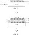
- FIGS. 1A and 1Bare diagrams showing the start of a process for direct-bonding dies of a first footprint size to dies of a second footprint size in a wafer level process.
- FIGS. 2A-2Care diagrams showing a continuation of the process of FIGS. 1A and 1B , for direct-bonding dies of a first footprint size to dies of a second footprint size in a wafer level process.
- FIGS. 3A-3Dare diagrams of example devices showing routing and interconnect variations in devices made by direct-bonding dies of a first footprint size to dies of a second footprint size in a wafer level process.
- FIGS. 4A-4Care diagrams of an example micropackage and molding encapsulation fabricated by direct-bonding dies of a first footprint size to dies of a second footprint size in a wafer level process.
- FIGS. 5A-5Eare diagrams of a process for producing multilayered structures of stacked dies, wherein variegated dies of the various layers have various sizes, types, and dimensions.
- FIGS. 6A-6Care diagrams of example interposers with variegated dies in multiple layers on one or both sides of the interposers by direct-bonding dies of a first footprint size to dies of a second footprint size in a wafer level process.
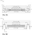
- FIGS. 7A and 7Bare diagrams of a first example backside illuminated image sensor structure.
- FIGS. 8A-8Care diagrams of a second example backside illuminated image sensor structure.
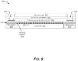
- FIG. 9is a diagram of a third example backside illuminated image sensor structure.
- FIGS. 10A and 10Bare diagrams of a fourth example backside illuminated image sensor structure.
- FIG. 11is a diagram of a first example front-side illuminated image sensor structure.
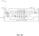
- FIG. 12is a diagram of a second example front-side illuminated image sensor structure.
- FIG. 13is a flow diagram of an example method of fabricating direct-bonded stacked die structures in a wafer level process.
- This disclosuredescribes stacked devices and associated methods of fabrication.
- Systems and methods described hereinenable die-to-wafer (D2W) or chip-to-wafer (C2W) techniques to bond layers of dies of various physical sizes, form factors, and foundry nodes (process nodes, technology nodes) to a semiconductor wafer, to interposers, or to boards and panels (all of these may be referred to herein as “substrates”).
- the example systems and methodsenable 3D stacking of variegated dies by direct hybrid bonding within a wafer level packaging (WLP) flow, including fan-out versions of 3D die stacks consisting of dies with different footprints—at the level of wafer level packaging.
- WLPwafer level packaging
- the systems and methodsenable direct-bonding of layers of variegated dies mixed and matched from various different foundry nodes (process nodes, technology nodes), different form factors, different wafer sizes, and different package physical sizes into vertical stacks within a single micropackage at wafer level, with the benefits of high interconnect density and space-saving provided by the direct hybrid bonding.
- the micropackageis an interposer
- the interposercan have the variegated dies on one or both sides, including dies of different geometries stacked vertically on one or both sides. Interposers bearing multiple types of dies of various physical sizes and foundry nodes, including stacks of such dies, can then be bonded to a semiconductor wafer, in one example scenario.
- example systems and methodsenable creation of micropackage architecture in which conventionally incompatible dies picked from wafers that differ from each other in technology, foundry node, wafer size, and form factor can be bonded together in the same micropackage at wafer level without much restriction, given a common interconnect interface between any two units being direct-bonded together.
- the example systems and methodsalso provide the advantage of high yield production, since variegated dies selected from different sources for direct-bonding and stacking to a wafer or interposer can be known-good-dies (KGDs).
- a foundry node(“technology node,” “process node,” “process technology,” or simply “node”) refers to a specific semiconductor manufacturing process and its design rules, and generally refers to a minimum feature size. Different nodes imply different architectures and circuits from different generations of the technology. Essentially, technology node refers to the physical size of the transistor being fabricated. The more recent the technology node, the smaller the transistors, with more transistors per unit area, which in turn provides faster switching, less energy use, and cooler operation than a previous version of the same technology node. Thus, smaller technology nodes generally have smaller feature sizes: smaller transistors that are faster and more power-efficient than those made according to an earlier node.
- Silicon wafer diameter nodesa different designation than foundry nodes, have progressed in the other direction, from smaller to larger.
- Recent silicon wafer diameter nodesare 150 mm, 200 mm, and 300 mm, with 450 mm on the horizon.
- Larger semiconductor wafersreduce the manufacturing cost per transistor by raising the integration level through device scaling and other factors such as improvement in production yield because of non-defect rate, and increased throughput in production volume per unit of time.
- the number of semiconductor dies obtainable from a waferalso increases, reducing the production cost per die. Larger, more recent wafer sizes tend to incorporate the latest technology nodes (smaller feature sizes).
- variable diesthat is, dies of different physical dimensions and different feature and technology sizes.
- an example process described hereindirect-bonds the variegated dies of various physical sizes, form factors, and/or foundry nodes to wafers of same or different size origin or foundry node, filling in lateral spaces caused by differences in physical sizes and form factors with a molding material to fill and complete a given horizontal bonding layer.
- the molding materialmay be a molding compound, a resist material, a glass, a silicon spacer material, or a thermally conductive compound.
- the interstitial molding materialmay be extremely thin vertically, matching the layer's vertical thickness determined by the heights of the dies being direct-bonded in that layer.
- the particular bonding layer of dies and moldingmay then be planarized with chemical-mechanical planarization (CMP) or other polishing technique at wafer level to prepare for a next bonding layer of variegated dies from various foundry nodes and wafer sizes to be direct-bonded to the previous layer.
- CMPchemical-mechanical planarization
- the example processallows continued stacking of the variegated dies and interstitial molding within each bonding layer, to make vertical stacks of the variegated dies in a microelectronics package.
- Conductive through-vias, interconnects, and/or leadscan be disposed in the molding material disposed laterally between the variegated dies of a given direct-bonding layer of dies. This allows horizontal fan-out of the leads of dies of a given layer, and also allows vertical transmission of signals between adjacent layers of dies, or through multiple layers of dies, without necessarily having to create any vias through the dies themselves.
- the coefficient of thermal expansion (CTE) of the molding material used in the example systems and methodsaims to match the CTE of silicon or other semiconductor substrate material in use.
- This match of the CTEs between semiconductor and moldingmakes the molding material amenable to expansion and contraction of the semiconductor material caused by thermal fluctuations during further steps of the fabrication process, and also amenable to thermal fluctuations during operation of the micropackage when in use as a “chip” in an end device.
- the hardness, density, friability, and other physical characteristics of the molding materialis ideally formulated to match those of silicon or other semiconductor, so that CMP and other polishing and finishing processes cannot distinguish between the molding material and the semiconductor, for purposes of polishing to a flat or ultra-flat surface that is free from significant dishing and rounding: and so immediately available for further direct-bonding steps in construction of vertical stacks of the variegated dies.
- direct-bondingis the only bonding process used between dies, between dies and wafer, and between dies and interposer, then intervening connection structures such as ball grid arrays may be eliminated to save space.
- direct-bonding between dies, or between dies and wafercan be between native interconnects of the logic circuits and other native circuits of the dies and wafers. This use of native interconnects direct-bonded together can save even more space, since in some cases standard interfaces may be eliminated during design of the variegated dies themselves.
- Suitable direct-bonding techniquesprepare surfaces for molecule-to-molecule, covalent, ionic, and/or metallic bonding between like materials on each side of the direct-bonding interface. For example, freshly prepared flat surfaces of copper metal (Cu) may bond to each other upon contact with or without pressure and heat, forming copper diffusion bonds, metal-to-metal bonds, and the like.
- Zibond® brand direct-bondingis one example direct-bonding technique for dielectrics, oxide materials, and other nonmetals (Xperi Corporation, San Jose, Calif.).
- Zibond® direct-bondingis a room temperature wafer-to-wafer or die-to-wafer direct-bonding technique.
- DBI® brand hybrid bondingis an example direct-bonding technique for joining nonmetal (e.g., dielectric) surfaces that also have metal interconnects to be joined together in the same planar bonding interface (Xperi Corporation, San Jose, Calif.).
- the DBI direct hybrid bondingmay be accomplished in one operation, in which oxide dielectric surfaces direct-bond together first, at room temperature, and then metal interconnects on each side of the bonding plane direct-bond together during an annealing phase at slightly or moderately elevated temperatures.
- the molding material introduced abovewhen used as a filler or plastic encapsulant, is conventionally found in micropackaging technologies, and is also used for making reconstituted wafers having a layer of chips or dies diced from a first wafer, and then joined to a second carrier wafer or panel in a single layer on the wafer or panel.
- such molding materials and various fillersmay be put to use in layers of a few mils (a mil is one-thousandth of an inch or 0.001 inch), and up to far greater thicknesses in construction of a 3DIC.
- the molding material suitable for the example systems and processes described hereinis applied to fill-in lateral spaces between dies but in much thinner vertical layers than used for reconstituting wafers, at a vertical height suitable for the dies in the layer being direct-bonded to a previous layer.
- the molding materialis recruited to the wafer fabrication environment to make ultra-flat surfaces for direct hybrid bonding between layers of variegated dies.
- a conventional process for making a reconstituted waferis limited to using the molding material as an encapsulant
- the example processes hereinare able to use the molding material to make surfaces suitable for direct-bonding stacks of variegated dies within the scope of the wafer level semiconductor fabrication process itself.
- Example systems and methodsare not limited to front-to-front direct hybrid bonding of dies to wafers, and front-to-front direct hybrid bonding of dies to other dies.
- front-to-front examples of stacked structuresmay be shown and described representatively herein, the direct bonding of dies to wafers or dies to dies according to the example system and methods described herein may be front-to-front, front-to-back, or back-to-back, when these possible configurations are desired in a given scenario.
- the use of handle wafers with intermediate temporary bond and debond stepsmay be used to present a back surface for bonding.
- FIGS. 1A and 1B and in all the figures described hereinthe layers illustrated are not shown to relative scale.
- layers of dielectric material and silicon that provide bonding layers and direct-bonding surfacesare shown with exaggerated thickness for the sake of illustration and description, and to emphasize their presence and their various features. Some of these layers of materials may be extremely thin layers, coatings, or deposits in actual microelectronic devices.
- the various diesmay be shown as direct-bonded to each other face-to-face, with direct hybrid bonding of both dielectric surfaces and metal interconnects between the dies at the bonding interfaces but the stacked structures shown and the related processes are not limited to face-to-face direct bonding of the dies.
- the dies on adjacent vertical layers of the example stacked structuresmay also be direct-bonded face-to-back and back-to-back in addition to the face-to-face direct bonding of the dies in the layers of the stacked structures.
- FIG. 1Ashows the start of an example process for making a microelectronic device using a wafer level process, including D2W techniques.
- a substratesuch as a wafer, has first dies 102 in a first layer 104 , and at least some of the first dies 102 have a first footprint size and specific physical dimensions.
- Second dies 106 in a second layer 108include dies with a second footprint size and/or different physical dimensions than the footprint size and physical dimensions of the first dies 102 in the first layer 104 .
- Dies 102 in the first layer 104have a front side layer of metal contacts 110 providing electrical contacts and/or redistribution traces for integrated circuits of the dies 102 .
- the metal contacts 110can be built up into a bonding layer with interconnects for direct-bonding to the second dies 106 , or in some cases the metal contacts 110 can be bonded directly to the second dies 106 without further buildup of redistribution layers RDLs or further vertical extension using through-vias.
- the second dies 106 residing in the second layer 108have a respective layer of metal 112 for making electrical contacts that can be built up through RDLs or by vertical extension by through-vias, or in some cases direct-bonded directly to the first dies 102 .
- dielectric (or silicon) layers 114 and 116are added to respective dies 102 and 106 to make direct hybrid bonding surfaces.
- through-viase.g., 118 and 120
- other interconnects or redistribution conductorsrise vertically through the dielectric layers 114 and 116 to metal bonding pads 122 and 124 on the surfaces of the respective dies 102 and 106 for eventual direct-bonding at a bonding interface 126 .
- the dielectric layers 114 and 116 and the respective metal bonding pads 122 and 124all participate in direct hybrid bonding at the bonding interface 126 .
- the two respective dielectric layers 114 and 116direct-bond to each other in dielectric-to-dielectric direct bonding, while the metal bonding pads 122 and 124 direct-bond to each other in metal-to-metal direct bonding, during an annealing phase of the same direct hybrid bonding operation, for example.
- the first dies 102 of the wafer, or on a substratemay be memory dies, sensor image dies, or other kinds of dies of various types and sizes.
- the second dies 106with different physical dimensions and/or different footprints than the first dies 102 , may be logic dies or other dies to be communicatively coupled with the first dies 102 .
- the first dies 102 and the second dies 106may be mixed and matched from different wafer sizes, different foundry nodes (process nodes, technology nodes), different footprints, different functionalities, different physical sizes, and so forth, referred to hereinafter as variegated dies.
- a molding material 200is applied to at least partially fill-in spaces that occur horizontally between the second dies 106 in the second layer 108 .
- the molding material 200ideally has a similar (CTE) as the dies 106 or dielectric 116 (or silicon) that the molding material 200 is intervening between.
- the molding materialmay be a compound such as a filler material, a resist compound, silicon, a high thermal conductivity compound, formed diamond, deposited diamond, formed aluminum nitride, deposited aluminum nitride, a material with a CTE close to a CTE of silicon, a packaging material, or a board material, for example.
- the wafer or substrate on which the first dies 102 residemay be thinned 202 , especially if the second layer of dies 106 is the only layer to be direct-bonded to the layer of first dies 102 .
- FIGS. 3A-3Dshow various ways in which first dies 102 of a wafer, carrier, or substrate that have been direct-bonded to seconds dies 106 of different size, footprint, wafer-origin, and/or foundry node can be interconnected externally, outside their own micropackage.
- a metallization layer 302 of the first dies 102has pad areas available that can be etched out of each die 102 (or wafer or substrate) to make electrical contacts, either for external connection or for continuance of the fabrication of the micropackage 300 .
- through silicon vias (TSVs) 306are made through the first dies 102 to enable backside electrical connection at backside contact pads 308 , for example, and/or construction of RDLs on the backside of the dies 102 or thinned wafer hosting the dies 102 .
- TSVs 312are made through the second dies 106 to enable electrical connection at backside contact pads 314 of the second dies 106 , for example, and/or to connect with RDLs to be fabricated on the backsides of the second dies 106 .
- Through-vias 316may also be constructed to pass through the molding material 200 that has been applied to at least partially fill the spaces between dies 106 of a given direct-bonded layer. Such through vias 316 and 318 through the molding material 200 can extend to either side of the entire micropackage 310 .
- Through-vias 320can also extend from the contact pads 122 of the first dies 102 , through the molding material 200 , to the backside of the second dies 106 or beyond (if there are additional direct-bonded layers of dies).
- through-vias 322can extend all the way through the entire example micropackage 310 , including through the molding material 200 , from one side of the example micropackage 310 to the other.
- various TSVs 306 and 312 and various through-vias 316 extending through the molding material 200can extend from the contact pads of dies 102 and 106 from multiple layers of the micropackage 324 , to both front and back sides of the microelectronics package 324 , traversing through the molding material 200 as needed.
- FIGS. 4A-4Cshow another example microelectronics package 400 with molding material between dies also encapsulating the dies or filling out package dimensions.
- first dies 402 of a first type, first footprint, and first dimensionsare direct-bonded to dies 404 of a second type, second footprint, and second dimensions, with intervening dielectric layers 114 and 116 .
- the dies 402 and 404are physically and electrically connected by direct hybrid bonding, in which the dielectric layers 114 and 116 direct-bond to each other with dielectric-to-dielectric direct bonds, and metal interconnects, pads, and/or vias direct-bond to each other across the bonding interface with metal-to-metal direct bonds.
- a molding material 406is applied to at least partially fill-in spaces that occur horizontally between the second dies 404 .
- the molding material 406also forms a layer 408 above the top of the second dies 404 , to encapsulate the dies 404 , complete the package, fill a void, and/or to form a filler layer 408 for continuing fabrication of the micropackage 400 above the top of the layer 408 of the molding material 406 .
- the molding material 406may also fill-in vertical spaces above some dies 404 of the second layer that are shorter in vertical height than other dies 404 of the second layer. Conductive leads of the shorter second dies 404 may be extended with through-vias to a top surface of the second layer of dies 404 , or to a next layer of dies, or to an outside surface of the example micropackage 400 .
- the molding material 406ideally has a similar CTE as the dies 404 or dielectric 116 (or silicon) that the molding material 406 is intervening between and/or encapsulating.
- the molding material 406may be a compound such as a filler material, a resist compound, silicon, a high thermal conductivity compound, formed diamond, deposited diamond, formed aluminum nitride, deposited aluminum nitride, a material with a CTE close to a CTE of silicon, a packaging material, or a board material, for example.
- through vias 410 and 412 and 414 and 416can extend from any contact pads of any of the dies 402 and 404 in the micropackage 400 to any side of the micropackage 400 for external connection, traversing through the molding material 406 as needed.
- the first dies 402 and/or the molding material 406may be thinned as needed for further layering or packaging.
- FIGS. 5A-5Cshow an example process for making a microelectronic device with variegated dies direct-bonded in multiple layers.
- the variegated dies of FIGS. 5A-5Ccan be logic dies, image sensor dies, high bandwidth memory (HBM) dies, and so forth.
- HBMhigh bandwidth memory
- all direct bonds or direct hybrid bonds shown between diescan be direct bonds formed between surfaces of the dies themselves, or can be direct bonds formed via one or more intervening dielectric bonding layers (not shown explicitly).
- the dielectric bonding layers(not shown in FIGS. 5A-5C ) can contain metal interconnects or through-vias for vertically extending electrical contacts through the dielectric bonding layers. Examples of dielectric layers 114 and 116 can be seen in FIGS. 1A, 1B, and 2A-2C .
- a substrate, carrier or wafer 100has first dies 102 , and at least some of the first dies 102 have a first footprint size and specific physical dimensions. Second dies 106 with a second footprint size and/or different physical dimensions than the footprint size and physical dimensions of the first dies 102 .
- molding material 500is placed horizontally between the dies 106 to at least partly fill the empty spaces between the dies 106 .
- the top surface of the second dies 106 and the molding material 500can be planarized to make a surface for direct bonding or direct hybrid bonding another layer of variegated dies on top of the second dies 106 .
- the planarizationcan be chemical mechanical polishing (CMP) to impart flatness and surface characteristics sufficient for direct bonding.
- third dies 502can be direct bonded or direct hybrid bonded to the second dies 106 .
- the third dies 502can be variegated dies with footprints, foundry nodes, wafer origins, functionalities, and physical dimensions different than second dies 106 , and may also be different than the first dies 102 .
- the various dies 102 and 106 and 502do not have to be different from each other in size, footprint, foundry node, functionality, and so forth, but the example process shown in FIG. 5 makes such stacking of variegated dies 102 and 106 and 502 possible in a wafer level process.
- FIG. 5Eanother round of molding material 504 , which may be the same material or a different material than molding material 500 used in the second layer, is applied between the third dies 502 in the third layer to at least partly fill the empty spaces horizontally between the dies 502 of the third layer.
- the top surfaces of the third dies 502 and the molding material 504 of the third layerare planarized to make a surface for direct bonding or direct hybrid bonding another layer of variegated dies, if desired, on top of the third layer of dies 502 .
- the planarizationcan be CMP to impart flatness and surface characteristics sufficient for direct bonding.
- the processcan continue with direct-bonding or direct hybrid bonding of each new layer of variegated dies, filling-in intervening spaces between dies of each new layer with molding material, and then planarizing the top of the dies and the molding material for direct bonding of the next layer of dies.
- Dies 102 in the first layer 104have a front side layer of metal contacts 110 providing electrical contacts and/or redistribution traces for integrated circuits of the dies 102 .
- the metal contacts 110can be built up into a bonding layer with interconnects for direct-bonding to the second dies 106 , or in some cases the metal contacts 110 can be bonded directly to the second dies 106 without further buildup of RDLs or further vertical extension using through-vias.
- conductive through-vias, conductive interconnects, leads, redistribution traces, fan-outs, and RDLscan be routed in the microelectronics package, including through the molding materials 500 and/or 504 , to connect the dies 502 and 506 and 514 to each other, and/or to contact pads on the outside of the microelectronics package.
- FIGS. 6A-6Cshow different example configurations of interposer devices built according to the processes described herein.
- the example interposerscan be used in 2.5D integrated circuit technology, for example, to provide several benefits.
- variegated dies of various different footprint sizes, types, foundry nodes, wafer origins, physical dimensions, and so forthcan be mixed and matched not only on one side, but on both sides of an interposer substrate that is silicon, organic, or other material.
- the included variegated diescan be bonded together into the interposer package with direct bonding techniques instead of solder ball arrays, for example, although solder ball arrays are not excluded.
- the direct bonding or direct hybrid bondingcan create ultra-high density routing between dies.
- KGDsknown good dies
- interposerscan then be reconstituted onto a semiconductor wafer, or other silicon or organic substrate, for example, or onto the package substrate of microelectronic devices making an efficient way to create such micropackages using wafer level processes to provide smaller size and higher bandwidth, and with less expensive techniques than are possible with conventional ball grid array interconnects and conventional wafer reconstitution processes.
- the example interposers shown and describedcan help to decrease interconnection length between multiple dies assembled on the example interposers. This increases the number of interconnection routes for the interposer with stacked structure of variegated dies, saves power consumption, decreases latency, and increases bandwidth compared to conventional interposers.
- a first example interposer 601has an interposer substrate 600 with a first layer of dies 602 and a second layer of different dies 604 direct-bonded to the first layer of dies 602 .
- a molding material 606at least partly fills-in the spaces between the dies 604 in the second layer.
- the molding material 606may also continue horizontally over the dies 604 to encapsulate the dies 604 (not shown) and complete the interposer package.
- the interposer 600may use one or more RDLs 608 to distribute or fan-out traces.
- Interconnects and through-vias 610can be leveraged anywhere in the package, including through the molding material 606 depending on application and need (not shown).
- the example through-vias 610can also pass through the interposer substrate 600 and connect to a package substrate, to a wafer, or even to another interposer via contact pads disposed on an external surface of the interposer substrate 600 , for example (not shown).
- a second example interposer 611 with an interposer substrate 612has a layer of first dies 614 of a first type, and a layer of second dies 616 of a second type direct-bonded to the first dies 614 .
- the dies 614 and 616may differ from each other in footprint size, functionalities, physical size, foundry node, wafer origin, and in many other specifications, but can be combined together in a wafer level process using the molding material 618 to make direct-bondable layers for making multiple levels of stacked dies 614 and 616 . . . n, in the example interposer.
- the interposer 611may interface with a wafer or other devices via its interposer substrate 612 or via die 616 positioned to present front contacts of backside TSV reveals to the interface (not shown).
- a third example interposer 621has an interposer substrate 620 , a layer of first dies 622 of a first type on distribution lines 623 or on one or more RDLs, for example, and a second layer of dies 624 of a second type direct-bonded to the first layer of dies 622 .
- the dies 622 and 624do not have to be different types, they can be the same type of die, but the example process and structures allows the dies 622 and 624 to be very different from each other.
- a molding material 625fills-in spaces between dies 624 of the second layer and can also encapsulate (not shown) the dies 624 or can encapsulate (not shown) the entire top side of the interposer package 621 .
- a third layer of dies 626are bonded and electrically connected if applicable, with another molding material 627 or the same molding material used above filling in spaces between dies 626 .
- a fourth layer of dies 628which is the second layer on this opposing side of the interposer substrate 620 are direct-bonded to the third layer of dies 626 , with another molding material 629 filling-in spaces between the dies 628 of the fourth layer and can also encapsulate (not shown) the dies 628 or can encapsulate (not shown) the entire bottom side of the interposer package 621 .
- Through-vias, distribution traces, and contact padscan be disposed anywhere in, or on the outside of the interposer package 621 , traversing any of the molding material 625 and 627 and 629 as needed for routing.
- the interposer package 621can interface with a wafer or other devices via either top or bottom connections, or both.
- the example interposers 601 and 611 and 621can be used to make HBMs, with high density routing. Memory dies can be stacked on the interposers along with dies providing the main processor and HBM controller.
- the example interposers 601 and 611 and 621can also be used for other high performance computing applications, artificial intelligence (AI), graphic processors, image sensors, and other applications.
- AIartificial intelligence
- Example image sensor devicesare now described as example embodiments of the stacked die structures and associated processes shown and described above in FIGS. 1A-6C . Both backside illuminated and front-side illuminated image sensors and associated methods of fabrication are described using the processes of making stacked die structures of FIGS. 1A-6C .
- Front-side illuminationrefers to light entering photo diode elements through a BEOL layer of metal wiring built on the front side of the photo diode elements.
- a bond interface with a logic chipis on the backside of the photo diode elements die, faced away from the incoming light.
- Back-side illuminationrefers to light entering the photo diode elements on the side of the backside of the photo diode elements die, with the BEOL metal wiring layer on the opposing front side of the photo elements die.
- the BEOL metal wiring layer(on the front side, away from the incoming light) faces the bond interface with the logic chip.
- CMOScomplementary metal-oxide semiconductor
- FIG. 7Ais a diagram of a first example backside illuminated image sensor structure 700 .
- the example backside illuminated image sensor structure 700can be made by direct hybrid bonding of logic dies 702 of a first footprint size, to a front side of an image sensor wafer 704 in a D2W process, and optionally filling-in spaces between the logic dies 702 , either fully or partly, with a molding compound 706 , a resist material, a silicon spacer material, glass, or a thermally conductive compound, for example.
- the direct hybrid bonding between photo diode element dies on the image sensor wafer 704 and the logic dies 702may be intermediated by dielectric layers 708 and 710 with through-vias 712 and 714 and contact pads 716 and 718 suitable for direct hybrid bonding.
- the image sensor wafer 704may be a 200 millimeter wafer, or of other size, and the logic dies 702 can also be of various sizes, for example logic dies 702 from a 300 millimeter wafer, for example.
- the direct hybrid bondingcan be a direct bond interconnect (DBI®) hybrid bonding process, for example, or other process that direct-bonds dielectric surfaces together while direct-bonding the metal contact pads 716 and 718 together in steps of the same direct-bonding operation.
- DI®direct bond interconnect
- a support carriermay optionally be direct bonded to at least the logic dies 702 using an intervening dielectric, for example.
- Imaging layerssuch as a color filter array 720 and on-chip lens 722 , for example, may be deposited, bonded or direct-bonded to the image sensor wafer 704 .
- Last metal contact pads 724 and 726may be etched out to make package interconnects, or other interconnect methodologies may be implemented through routing lines and through-vias, including routing lines and through-vias directed through the molding material 706 .
- An example process for making the example backside illuminated image sensor structure 700includes obtaining an image sensor wafer 704 that has photo-diode arrays or pixel arrays, the arrays of a first size.
- the example processcreates microcircuits and bonding pads on a front-side of the image sensor wafer 704 , the bonding pads suitable for direct hybrid bonding.
- the processcontinues with obtaining a logic die 702 of a second size, for example, the second size can be smaller than the first size of the photo-diode arrays or the pixel arrays of the image sensor wafer 704 .
- Microcircuits and bonding pads for direct hybrid bondingare also made on the logic die 702 .
- the example processjoins the logic die 702 to at least one photo-diode array or pixel array of the image sensor wafer 704 with a hybrid bonding technique to form a mechanical and electrical connection between the bonding pads of the logic die 702 and the bonding pads of the image sensor wafer 704 .
- the molding material 706may be added to extend the logic die, which may have a variety of sizes, to match the larger size of the photo-diode array or pixel array when needed, or to partially or fully fill in horizontal spaces in the horizontal layer containing the logic die(s) 702 .
- the molding material 706can be a molding compound, passive silicon, a glass, a thermally conductive material, or other suitable material.
- the filler materialmay also be formed or deposited diamond, formed or deposited aluminum nitride, a material with a CTE close to a CTE of silicon, a packaging material, and a board material, for example.
- the molding material 706may have a high thermal conductivity, and may extend below the logic dies 702 to dissipate heat and hot spots in the image sensor wafer 704 (not shown). The molding material 706 may also extend below the logic dies 702 to add mechanical strength to the layer of the logic dies 702 (not shown). If passive or dummy silicon is the filler material, the silicon may be applied as a spin coating, for example.
- FIG. 7Billustrates a structure 700 ′ that shows a variation of the example backside illuminated image sensor package 700 , in which access to the bonding pads 726 and 726 is obtained through vias created on the front side of the image sensor package 700 ′.
- the joiningmay direct-bond logic dies 702 of one size, from a 300 millimeter wafer, for example, to image sensor wafers 704 on a 200 millimeter image sensor wafer 704 , for example.
- the direct-bondingcan additionally be a direct hybrid bonding process, such as a DBI® hybrid bonding process for fine-pitch hybrid bonding.
- the bondingcan also be a direct oxide bonding process, such as oxide bonding in the context of TSVs, for the electrical interconnects.
- a suitable example oxide bonding technique for this scenariocan be a ZiBond® direct oxide bonding process, for example, or another direct-bonding process.
- the photo-diode arrays or pixel arrays of the image sensor wafer 704may comprise CMOS image sensors (CIS), or other types of image sensors.
- the logic dies 702may include logic driver circuitry or memory, such as DRAM, or both logic driver circuitry and DRAM memory for the photo-diode arrays or pixel arrays.
- the photo-diode arrays or pixel arraysare on a backside of the image sensor wafer 704 for BSI implementations, and the example process may include thinning the backside of the image sensor wafer 704 .
- the example processcontinues with depositing the color filter array 720 and an on-chip lens 722 onto the thinned backside of the image sensor wafer 704 . Then, the process includes creating openings to the contact pads 724 and 726 of the photo-diode arrays or pixel arrays through a backside of the image sensor wafer 704 .
- the contact pads 724 and 726are usually chip-to-package bonding sites. In a variation, openings to the contact pads 724 and 726 can also be made from the front-side 728 of the image sensor package, an in example backside illuminated image sensor structure 700 ′.
- the openings to the contact pads 724 and 726are made through the molding material 706 to the front-side 728 of the image sensor wafer 704 .
- the openings to the contact pads 724 and 726are made through a bond via array (BVA) process.
- FIG. 8Cshows a second example backside illuminated image sensor structure 801 , comprising a reconstituted wafer 800 an image sensor portion 802 of the package.
- a reconstituted wafer 800is fabricated by bonding logic dies 804 and 806 and vertically shorter logic die 808 , for example, to a carrier wafer 809 .
- the logic dies 804 and 806 and 808 and carrier 809may optionally be bonded or adhered to a back support 810 for extra strength if desired.
- Horizontal spaces between the logic dies 804 and 806 and 808are at least partially filled with a molding material 812 .
- a direct hybrid bonding layer 816 of dielectric material and metal interconnectstops off the reconstituted logic package 800 .
- an image sensor wafer 814 of optionally different size and foundry origin than the logic dies 804 and 806 and 808is surmounted by a color filter array 820 , and an on chip lens 822 .
- the image sensor wafer 814is thinned, and a direct hybrid bonding layer 818 of dielectric and metal interconnects is added.
- the reconstituted logic part of the package 800 and the image sensor portion of the package 802are now direct hybrid bonded together to make the backside illuminated image sensor. Bond pads of the thinned image sensor wafer 814 are exposed for connection to a microelectronic device.
- an example process for making the example backside illuminated image sensor structure 800 and 802 of FIG. 8includes creating conductive vias 807 in the carrier wafer 809 , bonding the logic dies 804 and 806 and 808 of a first footprint size, such as dies from a 300 millimeter wafer, to the conductive vias 807 of the carrier wafer 809 using direct hybrid bonding or a surface mount technology, adding the molding material 812 between the logic dies 804 and 806 and 808 to make a reconstituted logic wafer 800 on the carrier wafer 809 , thinning the carrier wafer 809 to expose the conductive vias 807 on an opposing side of the carrier wafer 809 , and adding a direct bonding layer 816 to the exposed conductive vias 807 of the carrier wafer 809 .
- An optional back support wafer 810may be attached to the reconstituted logic wafer.
- the example processfurther includes adding a direct bonding layer 818 to an image sensor wafer 814 , and then joining the reconstituted logic wafer 800 to the image sensor wafer 802 by bonding the respective direct hybrid bonding layers 816 and 818 to each other.
- the example processthen includes thinning a backside of the image sensor wafer 814 , and depositing a color filter array 820 and an on-chip lens 822 on the thinned backside of the image sensor wafer 814 .
- the processthen opens vias to contact pads 824 and 826 of the image sensor wafer 814 through the color filter array 820 and the on-chip lens 822 .
- the molding material 812may be a mold compound, a resist compound, silicon, a high thermal conductivity compound, formed or deposited diamond, formed or deposited aluminum nitride, a material with a CTE close to a CTE of silicon, a packaging material, and a board material.
- the molding materialmay have a high thermal conductivity and may extend below the logic dies 804 and 806 and 808 to dissipate heat and hot spots in the thinned image sensor wafer 814 (not shown).
- the molding material 812may also extend below the logic dies 804 and 806 and 808 to add a mechanical strength to the layer of the logic dies 804 and 806 and 808 (not shown).
- FIG. 9shows another example backside illuminated image sensor structure 900 .
- This example structure 900attaches logic dies 902 to a thinned handle wafer 910 during fabrication. Handle wafer 910 may also or alternatively be thinned after logic die 902 attachment.
- the example processcreates TSVs 905 through the handle wafer 910 for coupling the logic dies 902 to the thinned image sensor wafer 904 .
- the TSVs 905may be formed by a via first, via middle, or via last process and some or all of the interconnections could be made by more traditional means, including through the use of solder connections.
- An example process for making the example backside illuminated image sensor structure 900 of FIG. 9includes planarizing the image sensor wafer 904 to make a thinned image sensor wafer 904 that has chip-to-package conductive contact pads 924 and 926 and has conductive bonding pads for connection to the logic dies 902 .
- the processdirect-bonds a front-side of the thinned image sensor wafer 904 to a first handle wafer 910 , attaching a temporary second handle wafer (not shown) to a backside of the thinned image sensor wafer 904 using a temporary dielectric layer that is direct-bonded between a backside of the thinned image sensor wafer 904 and the temporary second handle wafer.
- Image sensor wafer 904may also or alternatively be thinned after direct-bonding to the first handle wafer 910 .
- the processthins the first handle wafer 910 attached to the front-side of the thinned image sensor wafer 904 , and creates the conductive TSVs 905 through the thinned first handle wafer 910 , with first ends of the TSVs 905 conductively coupled to the bonding pads of the image sensor wafer 904 .
- the processadds a layer of bonding pads to second ends of the TSVs 905 , then direct-bonds the logic dies 902 to the bonding pads on the thinned first handle wafer 910 .
- the processadds a molding compound 906 , resist material, or silicon spacers in the horizontal spaces around the logic dies 902 , then removes the temporary first handle wafer (not shown) and the temporary dielectric layer from the backside of the thinned image sensor wafer 904 .
- the processexposes the conductive contact pads 924 and 926 of the thinned image sensor wafer 904 from the backside of the thinned image sensor wafer 904 , and then deposits a color filter array 920 and an on-chip lens 922 onto the backside of the thinned image sensor wafer 904 .
- Conductive contact pads 924 and 926 of the thinned image sensor wafer 904may alternatively be exposed after deposition of the color filter array 920 and/or on-chip lens 922 .
- the thinned image sensor wafer 904may be a 200 millimeter wafer, and the logic dies can be from a 300 millimeter wafer, for example.
- the example processmay include direct hybrid bonding the logic dies 902 to the layer of bonding pads on the thinned first handle wafer 910 .
- the direct hybrid bondingmay be DBI® brand of direct hybrid bonding, for example.
- the example processmay include direct hybrid bonding the first ends of the TSVs 905 to the bonding pads of the image sensor wafer 904 .
- the temporary dielectric layercan be direct bonded between the backside of the thinned image sensor wafer 904 and the temporary second handle wafer (not shown) using a ZiBond® direct bonding process, for example.
- the image sensor wafer 904has a 3-10 micron thickness of silicon and less than a 5 micron thickness of BEOL layers.
- the first handle wafer 910can either be thinned to greater than approximately 10 microns for greater downstream mechanical integrity or thinned to less than approximately 10 microns for simplifying subsequent processing.
- the second handle wafer(not shown) can be a 200 millimeter wafer with an initial thickness of approximately 750 microns.
- a layer containing the logic dies and the molding compound, the resist material or silicon spacerscan be greater than 50 microns thick.
- the molding compound 906can be a mold material, a resist compound, silicon, a high thermal conductivity compound, formed or deposited diamond, formed or deposited aluminum nitride, a material with a CTE close to a CTE of silicon, a packaging material, and a board material.
- the molding compound 906may have a high thermal conductivity and may extend below the logic dies 902 in order to dissipate heat and hot spots in the thinned image sensor wafer 904 (not shown).
- the molding compound 906may also extend below the logic dies 902 to add mechanical strength to the layer of the logic dies 902 (not shown).
- FIG. 10A and/or 10Bshows another example backside illuminated image sensor structure 1000 , which features fabrication using a temporary image sensor handle wafer, without a permanently incorporated handle wafer 910 of FIG. 9 .
- An example process for making the image sensor structure 1000 of FIG. 10A and/or 10Bincludes planarizing an image sensor wafer 1004 to make a thinned image sensor wafer 1004 , wherein the thinned image sensor wafer has chip-to-package conductive contact pads 1024 and 1026 and has conductive bonding pads for connection to logic dies 1002 .
- the processdirect-bonds a front-side of the thinned image sensor wafer 1004 to a first handle wafer (not shown) via a first dielectric layer (not shown), then direct-bonds the backside of the thinned image sensor wafer 1004 to a second handle wafer (not shown) via a second dielectric layer.
- the processremoves the first handle wafer from the front side of the thinned image sensor wafer 1004 while leaving the first dielectric layer in place, adding direct hybrid bond conductors and through dielectric vias (TDVs) 1005 to the first dielectric layer to convert the first dielectric layer to a direct hybrid bonding layer 1010 .
- the processbonds logic dies 1002 to the direct hybrid bonding layer 1010 via direct hybrid bonds, and adds a molding compound 1006 into the horizontal spaces around the logic dies 1002 .
- the molding compound 1006can be a filler, a resist material, or silicon spacers, for example.
- the processthen removes the second handle wafer (not shown) and the second dielectric layer from the backside of the thinned image sensor wafer 1004 , and exposes the conductive contact pads 1024 and 1026 of the thinned image sensor wafer 1004 from the backside of the thinned image sensor wafer 1004 .
- the processdeposits a color filter array 1020 and an on-chip lens 1022 onto the backside of the thinned image sensor wafer 1004 .
- the thinned image sensor wafer 1004can be a 200 millimeter wafer, and the logic dies 1002 may be diced from a 300 millimeter wafer, for example.
- the molding compound 1006can be a filler material, a resist compound, silicon, a high thermal conductivity compound, formed or deposited diamond, formed or deposited aluminum nitride, a material with a CTE close to a CTE of silicon, a packaging material, and a board material.
- the molding compound 1006can have a high thermal conductivity and may extend below the logic dies 1002 as shown in FIG. 10B at 1028 to dissipate heat and hot spots in the thinned image sensor wafer 1004 , and/or provide mechanical strength to the layer of logic dies 1002 .
- FIG. 11shows a first example of a front-side illuminated image sensor structure 1100 , made via the example processes described with respect to FIGS. 1-6 .
- FIG. 11can be distinguished from the sensor structures of FIGS. 7A-10B , which are backside illuminated sensor structures.
- lightshines through BEOL layers 1106 on a front side of an image sensor wafer 1104 .
- An example process for fabricating the example front-side illuminated image sensor structure 1100includes building back-end-of-line (BEOL) layers 1106 on a front side of an image sensor wafer 1104 , direct-bonding a handle wafer (not shown) onto the BEOL layers via a dielectric layer (not shown), thinning a backside of the image sensor wafer 1104 to approximately 10 microns, for example; creating TSVs 1105 through the thinned image sensor wafer 1104 , building a direct hybrid bond layer 1107 conductively coupled with ends of the TSVs 1105 on the backside of the thinned image sensor wafer 1104 , and direct hybrid bonding logic dies 1102 to the direct hybrid bonding layer 1107 .
- BEOLback-end-of-line
- the example processfurther continues with adding a filler or molding material 1108 around the logic dies 1102 .
- the filler materialcan be a mold material 1108 , a resist compound, silicon, a high thermal conductivity compound, formed or deposited diamond, formed or deposited aluminum nitride, a material with a CTE close to a CTE of silicon, a packaging material, and a board material.
- the filler material 1108may have a high thermal conductivity and may extend below the logic dies 1102 to dissipate heat and hot spots in the thinned image sensor wafer 1104 and/or provide mechanical strength to the layer of logic dies 1102 (not shown).
- the example processcontinues with removing the handle layer (not shown) and the dielectric (not shown) layer from the (top of the) BEOL layers 1106 , opening contact pads 1114 and 1116 of the BEOL layers 1106 from a front side of the BEOL layers 1106 , and depositing a color filter array 1110 and an on-chip lens 1112 to the BEOL layers 1106 to complete a front-side illuminated image sensor structure 1100 with logic dies 1102 direct hybrid bonded to the backside of the thinned image sensor wafer 1104 .
- the thinned image sensor wafer 1104can be a 200 millimeter wafer, and the logic dies can be from a 300 millimeter wafer, for example.
- a thickness for the logic dies 1102can be selected that provides sufficient mechanical strength for the package, i.e. front-side illuminated image sensor structure 1100 .
- FIG. 12shows a second example front-side illuminated image sensor structure 1200 .
- This implementation of a front-side illuminated image sensor structure 1200uses molding material 1208 to fill-in packaging around logic dies 1206 of one size, bonded to image sensor substrate 1202 and pixel arrays 1204 of different sizes, all in a wafer level production process.
- An example process making the front-side illuminated image sensor structure 1200 of FIG. 12includes bonding a color filter array 1210 and on-chip lens 1212 to a front side of a pixel array 1204 on an image sensor substrate 1202 and then adding a cover glass 1214 over the on-chip lens 1212 .
- the example processthen thins the backside of the image sensor substrate 1202 , and creates though-vias 1205 and a direct hybrid bonding layer 1207 on the backside of the image sensor substrate 1202 .
- the processattached logic dies 1206 to the direct hybrid bonding layer 1207 on the backside of the image sensor substrate 1202 , and adds molding material 1208 or a high strength thermally conductive material laterally to the logic die 1206 and to the lateral edges of the image sensor substrate 1202 .
- the molding material 1208 or the high strength thermally conductive materialcan extend in a layer below the logic dies 1206 .
- the thinned image sensor substrate 1202can be from a 200 millimeter image sensor wafer, and the logic dies 1206 can be from a 300 millimeter wafer, for example.
- Contact pads 1216 and 1218 for package bondingare opened from the front side of the device.
- FIG. 13shows an example method 1300 of fabricating direct-bonded stacked die structures in a wafer level process. Operations of the example method 1300 are shown in individual blocks.
- a substrate with first dies in a first layeris obtained.
- a second layer of second diesis direct-bonded to the first dies in the first layer.
- a molding materialis applied between the second dies in the second layer.
- the second dies in the second layer, and the molding materialare planarized to form a surface suitable for direct hybrid bonding to a third layer of dies.
Landscapes
- Engineering & Computer Science (AREA)
- Microelectronics & Electronic Packaging (AREA)
- Power Engineering (AREA)
- Computer Hardware Design (AREA)
- Physics & Mathematics (AREA)
- Condensed Matter Physics & Semiconductors (AREA)
- General Physics & Mathematics (AREA)
- Manufacturing & Machinery (AREA)
- Wire Bonding (AREA)
- Solid State Image Pick-Up Elements (AREA)
Abstract
Description
Claims (15)
Priority Applications (4)
| Application Number | Priority Date | Filing Date | Title |
|---|---|---|---|
| US16/413,429US11276676B2 (en) | 2018-05-15 | 2019-05-15 | Stacked devices and methods of fabrication |
| US17/586,236US11916054B2 (en) | 2018-05-15 | 2022-01-27 | Stacked devices and methods of fabrication |
| US18/148,351US12401011B2 (en) | 2018-05-15 | 2022-12-29 | Stacked devices and methods of fabrication |
| US18/507,478US12347820B2 (en) | 2018-05-15 | 2023-11-13 | Stacked devices and methods of fabrication |
Applications Claiming Priority (2)
| Application Number | Priority Date | Filing Date | Title |
|---|---|---|---|
| US201862671917P | 2018-05-15 | 2018-05-15 | |
| US16/413,429US11276676B2 (en) | 2018-05-15 | 2019-05-15 | Stacked devices and methods of fabrication |
Related Child Applications (1)
| Application Number | Title | Priority Date | Filing Date |
|---|---|---|---|
| US17/586,236ContinuationUS11916054B2 (en) | 2018-05-15 | 2022-01-27 | Stacked devices and methods of fabrication |
Publications (2)
| Publication Number | Publication Date |
|---|---|
| US20190355706A1 US20190355706A1 (en) | 2019-11-21 |
| US11276676B2true US11276676B2 (en) | 2022-03-15 |
Family
ID=68533093
Family Applications (4)
| Application Number | Title | Priority Date | Filing Date |
|---|---|---|---|
| US16/413,429ActiveUS11276676B2 (en) | 2018-05-15 | 2019-05-15 | Stacked devices and methods of fabrication |
| US17/586,236Active2039-08-09US11916054B2 (en) | 2018-05-15 | 2022-01-27 | Stacked devices and methods of fabrication |
| US18/148,351Active2040-06-16US12401011B2 (en) | 2018-05-15 | 2022-12-29 | Stacked devices and methods of fabrication |
| US18/507,478Active2039-07-10US12347820B2 (en) | 2018-05-15 | 2023-11-13 | Stacked devices and methods of fabrication |
Family Applications After (3)
| Application Number | Title | Priority Date | Filing Date |
|---|---|---|---|
| US17/586,236Active2039-08-09US11916054B2 (en) | 2018-05-15 | 2022-01-27 | Stacked devices and methods of fabrication |
| US18/148,351Active2040-06-16US12401011B2 (en) | 2018-05-15 | 2022-12-29 | Stacked devices and methods of fabrication |
| US18/507,478Active2039-07-10US12347820B2 (en) | 2018-05-15 | 2023-11-13 | Stacked devices and methods of fabrication |
Country Status (1)
| Country | Link |
|---|---|
| US (4) | US11276676B2 (en) |
Cited By (82)
| Publication number | Priority date | Publication date | Assignee | Title |
|---|---|---|---|---|
| US11462419B2 (en) | 2018-07-06 | 2022-10-04 | Invensas Bonding Technologies, Inc. | Microelectronic assemblies |
| US11515202B2 (en) | 2005-08-11 | 2022-11-29 | Adeia Semiconductor Bonding Technologies Inc. | 3D IC method and device |
| US11515279B2 (en) | 2018-04-11 | 2022-11-29 | Adeia Semiconductor Bonding Technologies Inc. | Low temperature bonded structures |
| US11600542B2 (en) | 2017-12-22 | 2023-03-07 | Adeia Semiconductor Bonding Technologies Inc. | Cavity packages |
| US11610846B2 (en) | 2019-04-12 | 2023-03-21 | Adeia Semiconductor Bonding Technologies Inc. | Protective elements for bonded structures including an obstructive element |
| US11621246B2 (en) | 2019-03-29 | 2023-04-04 | Adeia Semiconductor Technologies Llc | Diffused bitline replacement in stacked wafer memory |
| US11626363B2 (en) | 2016-12-29 | 2023-04-11 | Adeia Semiconductor Bonding Technologies Inc. | Bonded structures with integrated passive component |
| US11631586B2 (en) | 2012-08-30 | 2023-04-18 | Adeia Semiconductor Bonding Technologies Inc. | Heterogeneous annealing method |
| US11631647B2 (en) | 2020-06-30 | 2023-04-18 | Adeia Semiconductor Bonding Technologies Inc. | Integrated device packages with integrated device die and dummy element |
| US20230140107A1 (en)* | 2021-10-28 | 2023-05-04 | Adeia Semiconductor Bonding Technologies Inc. | Direct bonding methods and structures |
| US20230145518A1 (en)* | 2021-11-05 | 2023-05-11 | Nanya Technology Corporation | Die bonding structure, stack structure, and method of forming die bonding structure |
| US11652083B2 (en) | 2017-05-11 | 2023-05-16 | Adeia Semiconductor Bonding Technologies Inc. | Processed stacked dies |
| US20230154816A1 (en)* | 2021-11-17 | 2023-05-18 | Adeia Semiconductor Bonding Technologies Inc. | Thermal bypass for stacked dies |
| US11658173B2 (en) | 2016-05-19 | 2023-05-23 | Adeia Semiconductor Bonding Technologies Inc. | Stacked dies and methods for forming bonded structures |
| US11664357B2 (en) | 2018-07-03 | 2023-05-30 | Adeia Semiconductor Bonding Technologies Inc. | Techniques for joining dissimilar materials in microelectronics |
| US11670615B2 (en) | 2016-12-21 | 2023-06-06 | Adeia Semiconductor Bonding Technologies Inc. | Bonded structures |
| US11694925B2 (en) | 2017-10-06 | 2023-07-04 | Adeia Semiconductor Bonding Technologies Inc. | Diffusion barrier collar for interconnects |
| US11710718B2 (en) | 2015-07-10 | 2023-07-25 | Adeia Semiconductor Technologies Llc | Structures and methods for low temperature bonding using nanoparticles |
| US11715730B2 (en) | 2017-03-16 | 2023-08-01 | Adeia Semiconductor Technologies Llc | Direct-bonded LED arrays including optical elements configured to transmit optical signals from LED elements |
| US11721653B2 (en) | 2019-12-23 | 2023-08-08 | Adeia Semiconductor Bonding Technologies Inc. | Circuitry for electrical redundancy in bonded structures |
| US11728313B2 (en) | 2018-06-13 | 2023-08-15 | Adeia Semiconductor Bonding Technologies Inc. | Offset pads over TSV |
| US11728287B2 (en) | 2019-04-12 | 2023-08-15 | Adeia Semiconductor Bonding Technologies Inc. | Wafer-level bonding of obstructive elements |
| US11728273B2 (en) | 2020-09-04 | 2023-08-15 | Adeia Semiconductor Bonding Technologies Inc. | Bonded structure with interconnect structure |
| US11735523B2 (en) | 2020-05-19 | 2023-08-22 | Adeia Semiconductor Bonding Technologies Inc. | Laterally unconfined structure |
| US11742314B2 (en) | 2020-03-31 | 2023-08-29 | Adeia Semiconductor Bonding Technologies Inc. | Reliable hybrid bonded apparatus |
| US11742315B2 (en) | 2017-04-21 | 2023-08-29 | Adeia Semiconductor Bonding Technologies Inc. | Die processing |
| US11756880B2 (en) | 2018-10-22 | 2023-09-12 | Adeia Semiconductor Bonding Technologies Inc. | Interconnect structures |
| US11760059B2 (en) | 2003-05-19 | 2023-09-19 | Adeia Semiconductor Bonding Technologies Inc. | Method of room temperature covalent bonding |
| US11762200B2 (en) | 2019-12-17 | 2023-09-19 | Adeia Semiconductor Bonding Technologies Inc. | Bonded optical devices |
| US11764189B2 (en) | 2018-07-06 | 2023-09-19 | Adeia Semiconductor Bonding Technologies Inc. | Molded direct bonded and interconnected stack |
| US11764177B2 (en) | 2020-09-04 | 2023-09-19 | Adeia Semiconductor Bonding Technologies Inc. | Bonded structure with interconnect structure |
| US11790219B2 (en) | 2017-08-03 | 2023-10-17 | Adeia Semiconductor Inc. | Three dimensional circuit implementing machine trained network |
| US11791307B2 (en) | 2018-04-20 | 2023-10-17 | Adeia Semiconductor Bonding Technologies Inc. | DBI to SI bonding for simplified handle wafer |
| US11804377B2 (en) | 2018-04-05 | 2023-10-31 | Adeia Semiconductor Bonding Technologies, Inc. | Method for preparing a surface for direct-bonding |
| US11817409B2 (en) | 2019-01-14 | 2023-11-14 | Adeia Semiconductor Bonding Technologies Inc. | Directly bonded structures without intervening adhesive and methods for forming the same |
| US11842894B2 (en) | 2019-12-23 | 2023-12-12 | Adeia Semiconductor Bonding Technologies Inc. | Electrical redundancy for bonded structures |
| US11848284B2 (en) | 2019-04-12 | 2023-12-19 | Adeia Semiconductor Bonding Technologies Inc. | Protective elements for bonded structures |
| US11855064B2 (en) | 2018-02-15 | 2023-12-26 | Adeia Semiconductor Bonding Technologies Inc. | Techniques for processing devices |
| US11862604B2 (en) | 2018-06-22 | 2024-01-02 | Adeia Semiconductor Inc. | Systems and methods for releveled bump planes for chiplets |
| US11862602B2 (en) | 2019-11-07 | 2024-01-02 | Adeia Semiconductor Technologies Llc | Scalable architecture for reduced cycles across SOC |
| US11860415B2 (en) | 2018-02-26 | 2024-01-02 | Adeia Semiconductor Bonding Technologies Inc. | Integrated optical waveguides, direct-bonded waveguide interface joints, optical routing and interconnects |
| US11876076B2 (en) | 2019-12-20 | 2024-01-16 | Adeia Semiconductor Technologies Llc | Apparatus for non-volatile random access memory stacks |
| US11881454B2 (en) | 2016-10-07 | 2024-01-23 | Adeia Semiconductor Inc. | Stacked IC structure with orthogonal interconnect layers |
| US11894326B2 (en) | 2017-03-17 | 2024-02-06 | Adeia Semiconductor Bonding Technologies Inc. | Multi-metal contact structure |
| US11894345B2 (en) | 2018-08-28 | 2024-02-06 | Adeia Semiconductor Inc. | Integrated voltage regulator and passive components |
| US11901281B2 (en) | 2019-03-11 | 2024-02-13 | Adeia Semiconductor Bonding Technologies Inc. | Bonded structures with integrated passive component |
| US11908739B2 (en) | 2017-06-05 | 2024-02-20 | Adeia Semiconductor Technologies Llc | Flat metal features for microelectronics applications |
| US11916054B2 (en) | 2018-05-15 | 2024-02-27 | Adeia Semiconductor Bonding Technologies Inc. | Stacked devices and methods of fabrication |
| US11929347B2 (en) | 2020-10-20 | 2024-03-12 | Adeia Semiconductor Technologies Llc | Mixed exposure for large die |
| US11948847B2 (en) | 2017-12-22 | 2024-04-02 | Adeia Semiconductor Bonding Technologies Inc. | Bonded structures |
| US11955393B2 (en) | 2018-05-14 | 2024-04-09 | Adeia Semiconductor Bonding Technologies Inc. | Structures for bonding elements including conductive interface features |
| US11955445B2 (en) | 2018-06-13 | 2024-04-09 | Adeia Semiconductor Bonding Technologies Inc. | Metal pads over TSV |
| US11955463B2 (en) | 2019-06-26 | 2024-04-09 | Adeia Semiconductor Bonding Technologies Inc. | Direct bonded stack structures for increased reliability and improved yield in microelectronics |
| US11967575B2 (en) | 2018-08-29 | 2024-04-23 | Adeia Semiconductor Bonding Technologies Inc. | Bond enhancement structure in microelectronics for trapping contaminants during direct-bonding processes |
| US11973056B2 (en) | 2016-10-27 | 2024-04-30 | Adeia Semiconductor Technologies Llc | Methods for low temperature bonding using nanoparticles |
| US11978681B2 (en) | 2019-04-22 | 2024-05-07 | Adeia Semiconductor Bonding Technologies Inc. | Mitigating surface damage of probe pads in preparation for direct bonding of a substrate |
| US12009338B2 (en) | 2020-03-19 | 2024-06-11 | Adeia Semiconductor Bonding Technologies Inc. | Dimension compensation control for directly bonded structures |
| US12051621B2 (en) | 2016-12-28 | 2024-07-30 | Adeia Semiconductor Bonding Technologies Inc. | Microelectronic assembly from processed substrate |
| US12074092B2 (en) | 2018-05-30 | 2024-08-27 | Adeia Semiconductor Inc. | Hard IP blocks with physically bidirectional passageways |
| US12080672B2 (en) | 2019-09-26 | 2024-09-03 | Adeia Semiconductor Bonding Technologies Inc. | Direct gang bonding methods including directly bonding first element to second element to form bonded structure without adhesive |
| US12100676B2 (en) | 2018-04-11 | 2024-09-24 | Adeia Semiconductor Bonding Technologies Inc. | Low temperature bonded structures |
| US12113054B2 (en) | 2019-10-21 | 2024-10-08 | Adeia Semiconductor Technologies Llc | Non-volatile dynamic random access memory |
| US12136605B2 (en) | 2018-08-31 | 2024-11-05 | Adeia Semiconductor Bonding Technologies Inc. | Layer structures for making direct metal-to-metal bonds at low temperatures in microelectronics and method for forming the same |
| US12142528B2 (en) | 2016-10-07 | 2024-11-12 | Adeia Semiconductor Inc. | 3D chip with shared clock distribution network |
| US12154880B2 (en) | 2018-12-18 | 2024-11-26 | Adeia Semiconductor Bonding Technologies Inc. | Method and structures for low temperature device bonding |
| US12174246B2 (en) | 2019-05-23 | 2024-12-24 | Adeia Semiconductor Bonding Technologies Inc. | Security circuitry for bonded structures |
| US12191267B2 (en) | 2019-03-01 | 2025-01-07 | Adeia Semiconductor Technologies, LLC | Nanowire bonding interconnect for fine-pitch microelectronics |
| US12211809B2 (en) | 2020-12-30 | 2025-01-28 | Adeia Semiconductor Bonding Technologies Inc. | Structure with conductive feature and method of forming same |
| WO2025064195A1 (en)* | 2023-09-18 | 2025-03-27 | Adeia Semiconductor Bonding Technologies Inc. | Direct bonding methods and structures for dies |
| US12270970B2 (en) | 2018-03-20 | 2025-04-08 | Adeia Semiconductor Bonding Technologies Inc. | Direct-bonded lamination for improved image clarity in optical devices |
| US12272730B2 (en) | 2018-03-29 | 2025-04-08 | Adeia Semiconductor Inc. | Transistor level interconnection methodologies utilizing 3D interconnects |
| US12300634B2 (en) | 2021-08-02 | 2025-05-13 | Adeia Semiconductor Bonding Technologies Inc. | Protective semiconductor elements for bonded structures |
| US12322667B2 (en) | 2017-03-21 | 2025-06-03 | Adeia Semiconductor Bonding Technologies Inc. | Seal for microelectronic assembly |
| US12341083B2 (en) | 2023-02-08 | 2025-06-24 | Adeia Semiconductor Bonding Technologies Inc. | Electronic device cooling structures bonded to semiconductor elements |
| US12374556B2 (en) | 2016-12-28 | 2025-07-29 | Adeia Semiconductor Bonding Technologies Inc. | Processing stacked substrates |
| US12374641B2 (en) | 2019-06-12 | 2025-07-29 | Adeia Semiconductor Bonding Technologies Inc. | Sealed bonded structures and methods for forming the same |
| US12374656B2 (en) | 2017-06-15 | 2025-07-29 | Adeia Semiconductor Bonding Technologies Inc. | Multi-chip modules formed using wafer-level processing of a reconstituted wafer |
| US12381168B2 (en) | 2015-08-25 | 2025-08-05 | Adeia Semiconductor Bonding Technologies Inc. | Conductive barrier direct hybrid bonding |
| US12381173B2 (en) | 2017-09-24 | 2025-08-05 | Adeia Semiconductor Bonding Technologies Inc. | Direct hybrid bonding of substrates having microelectronic components with different profiles and/or pitches at the bonding interface |
| US12381128B2 (en) | 2020-12-28 | 2025-08-05 | Adeia Semiconductor Bonding Technologies Inc. | Structures with through-substrate vias and methods for forming the same |
| US12406959B2 (en) | 2018-07-26 | 2025-09-02 | Adeia Semiconductor Bonding Technologies Inc. | Post CMP processing for hybrid bonding |
| US12424584B2 (en) | 2020-10-29 | 2025-09-23 | Adeia Semiconductor Bonding Technologies Inc. | Direct bonding methods and structures |
Families Citing this family (36)
| Publication number | Priority date | Publication date | Assignee | Title |
|---|---|---|---|---|
| US11201187B2 (en)* | 2019-02-27 | 2021-12-14 | Ningbo Semiconductor International Corporation | CMOS image sensor packaging structure and fabrication method thereof, and camera device |
| US11158761B2 (en) | 2019-05-07 | 2021-10-26 | Facebook Technologies, Llc | Bonding methods for light emitting diodes |
| JP7496541B2 (en)* | 2020-01-30 | 2024-06-07 | パナソニックIpマネジメント株式会社 | Photodetector |
| DE102020116340B4 (en)* | 2020-02-27 | 2025-01-16 | Taiwan Semiconductor Manufacturing Co., Ltd. | STACKED IMAGE SENSOR DEVICE AND ITS MANUFACTURING METHOD |
| US11335657B2 (en)* | 2020-09-16 | 2022-05-17 | International Business Machines Corporation | Wafer scale supercomputer |
| US12261186B2 (en)* | 2021-03-25 | 2025-03-25 | Raytheon Company | Mosaic focal plane array |
| KR20220150137A (en) | 2021-05-03 | 2022-11-10 | 삼성전자주식회사 | Semiconductor package |
| US12341114B2 (en)* | 2021-06-14 | 2025-06-24 | Intel Corporation | Microelectronic assemblies having a hybrid bonded interposer for die-to-die fan-out scaling |
| WO2022261815A1 (en)* | 2021-06-15 | 2022-12-22 | 华为技术有限公司 | Chip stacking structure and manufacturing method, wafer stacking structure, and electronic device |
| CN117461136A (en)* | 2021-06-17 | 2024-01-26 | 半导体元件工业有限责任公司 | Stacked integrated circuit dies and interconnect structures |
| CN113594152B (en)* | 2021-07-12 | 2024-03-19 | 南京国博电子股份有限公司 | Three-dimensional integrated module of heavy-current PMOS tube and driver |
| US20230207522A1 (en)* | 2021-12-24 | 2023-06-29 | Intel Corporation | Reconstituted wafer-to-wafer hybrid bonding interconnect architecture with known good dies |
| US12191233B2 (en) | 2022-07-28 | 2025-01-07 | Adeia Semiconductor Bonding Technologies Inc. | Embedded cooling systems and methods of manufacturing embedded cooling systems |
| CN115424996A (en)* | 2022-08-16 | 2022-12-02 | 海光信息技术股份有限公司 | Interposer, method for forming the same, and package structure |
| US12232332B2 (en) | 2022-09-15 | 2025-02-18 | Tetramem Inc. | Integrated sensing and machine learning processing devices |
| US20240095512A1 (en)* | 2022-09-15 | 2024-03-21 | Tetramem Inc. | Integrated sensing and machine learning processing devices |
| US20240105704A1 (en)* | 2022-09-22 | 2024-03-28 | Apple Inc. | 3D Package with Chip-on-Reconstituted Wafer or Reconstituted Wafer-on-Reconstituted Wafer Bonding |
| US20240103238A1 (en)* | 2022-09-22 | 2024-03-28 | Apple Inc. | 3D System and Wafer Reconstitution with Mid-layer Interposer |
| WO2024138186A1 (en) | 2022-12-23 | 2024-06-27 | Adeia Semiconductor Bonding Technologies Inc. | Embedded cooling systems for advanced device packaging |
| US20240249995A1 (en)* | 2022-12-23 | 2024-07-25 | Adeia Semiconductor Bonding Technologies Inc. | Thermoelectric cooling addition |
| KR20250130348A (en) | 2022-12-29 | 2025-09-01 | 아데이아 세미컨덕터 본딩 테크놀로지스 인코포레이티드 | Embedded cooling assembly for advanced device packaging and method for manufacturing the same |
| KR20250130375A (en) | 2022-12-31 | 2025-09-01 | 아데이아 세미컨덕터 본딩 테크놀로지스 인코포레이티드 | Embedded liquid cooling technology |
| WO2024160459A1 (en)* | 2023-01-31 | 2024-08-08 | Ams-Osram Ag | Wafer structure, optical sensor, and corresponding method of production |
| US20240281390A1 (en)* | 2023-02-22 | 2024-08-22 | Micron Technology, Inc. | Memory device with 4n and 8n die stacks |
| WO2024206814A1 (en)* | 2023-03-31 | 2024-10-03 | Adeia Semiconductor Bonding Technologies Inc. | Direct hybrid bonding in topographic packages |
| TW202516697A (en) | 2023-03-31 | 2025-04-16 | 美商艾德亞半導體接合科技有限公司 | Integrated cooling assemblies including backside power/ground delivery and methods of manufacturing the same |
| US12191234B2 (en) | 2023-05-17 | 2025-01-07 | Adeia Semiconductor Bonding Technologies Inc. | Integrated cooling assemblies for advanced device packaging and methods of manufacturing the same |
| US20240387323A1 (en) | 2023-05-17 | 2024-11-21 | Adeia Semiconductor Bonding Technologies Inc. | Integrated cooling assemblies including signal redistribution and methods of manufacturing the same |
| US20250112192A1 (en)* | 2023-09-29 | 2025-04-03 | Apple Inc. | 3D System and Wafer Reconstitution with Mid-layer Interposer based on µbump |
| US12283490B1 (en) | 2023-12-21 | 2025-04-22 | Adeia Semiconductor Bonding Technologies Inc. | Integrated cooling assemblies for advanced device packaging and methods of manufacturing the same |
| US12368087B2 (en) | 2023-12-26 | 2025-07-22 | Adeia Semiconductor Bonding Technologies Inc. | Embedded cooling systems for advanced device packaging and methods of manufacturing the same |
| US12322677B1 (en) | 2024-02-07 | 2025-06-03 | Adeia Semiconductor Bonding Technologies Inc. | Fluid channel geometry optimizations to improve cooling efficiency |
| US12336141B1 (en) | 2024-03-29 | 2025-06-17 | Adeia Semiconductor Bonding Technologies Inc. | Cold plate cavity designs for improved thermal performance |
| US12176264B1 (en) | 2024-03-29 | 2024-12-24 | Adeia Semiconductor Bonding Technologies Inc. | Manifold designs for embedded liquid cooling in a package |
| US12266545B1 (en) | 2024-05-24 | 2025-04-01 | Adeia Semiconductor Bonding Technologies Inc. | Structures and methods for integrated cold plate in XPUs and memory |
| US12412808B1 (en) | 2024-12-20 | 2025-09-09 | Adeia Semiconductor Bonding Technologies Inc. | Cold plate and manifold integration for high reliability |
Citations (99)
| Publication number | Priority date | Publication date | Assignee | Title |
|---|---|---|---|---|
| US5753536A (en) | 1994-08-29 | 1998-05-19 | Matsushita Electric Industrial Co., Ltd. | Semiconductor device and associated fabrication method |
| US5771555A (en) | 1993-11-01 | 1998-06-30 | Matsushita Electric Industrial Co., Ltd. | Method for producing an electronic component using direct bonding |
| US6080640A (en) | 1997-07-11 | 2000-06-27 | Advanced Micro Devices, Inc. | Metal attachment method and structure for attaching substrates at low temperatures |
| US20020003307A1 (en) | 2000-07-05 | 2002-01-10 | Tadatomo Suga | Semiconductor device and method for fabricating the device |
| US6423640B1 (en) | 2000-08-09 | 2002-07-23 | Taiwan Semiconductor Manufacturing Co., Ltd. | Headless CMP process for oxide planarization |
| US6465892B1 (en) | 1999-04-13 | 2002-10-15 | Oki Electric Industry Co., Ltd. | Interconnect structure for stacked semiconductor device |
| JP2002353416A (en) | 2001-05-25 | 2002-12-06 | Sony Corp | Semiconductor storage device and method of manufacturing the same |
| US20040084414A1 (en) | 2002-08-19 | 2004-05-06 | Kenji Sakai | Polishing method and polishing composition used for polishing |
| US6887769B2 (en) | 2002-02-06 | 2005-05-03 | Intel Corporation | Dielectric recess for wafer-to-wafer and die-to-die metal bonding and method of fabricating the same |
| WO2005043584A2 (en) | 2003-10-21 | 2005-05-12 | Ziptronix, Inc. | Single mask via method and device |
| US6908027B2 (en) | 2003-03-31 | 2005-06-21 | Intel Corporation | Complete device layer transfer without edge exclusion via direct wafer bonding and constrained bond-strengthening process |
| US20060057945A1 (en) | 2004-09-16 | 2006-03-16 | Chia-Lin Hsu | Chemical mechanical polishing process |
| US7045453B2 (en) | 2002-10-24 | 2006-05-16 | International Business Machines Corporation | Very low effective dielectric constant interconnect structures and methods for fabricating the same |
| US7105980B2 (en) | 2002-07-03 | 2006-09-12 | Sawtek, Inc. | Saw filter device and method employing normal temperature bonding for producing desirable filter production and performance characteristics |
| US7193423B1 (en) | 2005-12-12 | 2007-03-20 | International Business Machines Corporation | Wafer-to-wafer alignments |
| US20070111386A1 (en) | 2002-02-20 | 2007-05-17 | Kim Sarah E | Process of vertically stacking multiple wafers supporting different active integrated circuit (IC) devices |
| US7750488B2 (en) | 2006-07-10 | 2010-07-06 | Tezzaron Semiconductor, Inc. | Method for bonding wafers to produce stacked integrated circuits |
| US7803693B2 (en) | 2007-02-15 | 2010-09-28 | John Trezza | Bowed wafer hybridization compensation |
| US7843052B1 (en)* | 2008-11-13 | 2010-11-30 | Amkor Technology, Inc. | Semiconductor devices and fabrication methods thereof |
| US7932616B2 (en)* | 2007-04-04 | 2011-04-26 | Spansion Llc | Semiconductor device sealed in a resin section and method for manufacturing the same |
| US20110186977A1 (en)* | 2010-01-29 | 2011-08-04 | Stats Chippac, Ltd. | Semiconductor Device and Method of Forming Thin Profile WLCSP with Vertical Interconnect over Package Footprint |
| US20120049344A1 (en)* | 2010-08-25 | 2012-03-01 | Stats Chippac, Ltd. | Semiconductor Device and Method of Forming FO-WLCSP with Discrete Semiconductor Components Mounted Under and Over Semiconductor Die |
| US20120217644A1 (en)* | 2011-02-24 | 2012-08-30 | Stats Chippac, Ltd. | Semiconductor Device and Method of Forming Conductive THV and RDL on Opposite Sides of Semiconductor Die for RDL-to-RDL Bonding |
| US20120282735A1 (en)* | 2011-05-02 | 2012-11-08 | Ahn Jung-Seok | Method of manufacturing chip-stacked semiconductor package |
| US20120292745A1 (en)* | 2011-05-20 | 2012-11-22 | Stats Chippac, Ltd. | Semiconductor Device and Method of Forming 3D Semiconductor Package with Semiconductor Die Stacked Over Semiconductor Wafer |
| US8349635B1 (en) | 2008-05-20 | 2013-01-08 | Silicon Laboratories Inc. | Encapsulated MEMS device and method to form the same |
| JP2013033786A (en) | 2011-08-01 | 2013-02-14 | Sony Corp | Semiconductor device and semiconductor device manufacturing method |
| US8377798B2 (en) | 2010-11-10 | 2013-02-19 | Taiwan Semiconductor Manufacturing Co., Ltd | Method and structure for wafer to wafer bonding in semiconductor packaging |
| US20130082399A1 (en)* | 2011-10-04 | 2013-04-04 | Won-keun Kim | Semiconductor package and method of manufacturing the same |
| US8441131B2 (en) | 2011-09-12 | 2013-05-14 | Globalfoundries Inc. | Strain-compensating fill patterns for controlling semiconductor chip package interactions |
| US8476165B2 (en) | 2009-04-01 | 2013-07-02 | Tokyo Electron Limited | Method for thinning a bonding wafer |
| US8482132B2 (en) | 2009-10-08 | 2013-07-09 | International Business Machines Corporation | Pad bonding employing a self-aligned plated liner for adhesion enhancement |
| US8501537B2 (en) | 2011-03-31 | 2013-08-06 | Soitec | Methods for bonding semiconductor structures involving annealing processes, and bonded semiconductor structures formed using such methods |
| US8524533B2 (en) | 2003-02-07 | 2013-09-03 | Ziptronix, Inc. | Room temperature metal direct bonding |
| US20130334697A1 (en)* | 2012-06-14 | 2013-12-19 | HanGil Shin | Integrated circuit packaging system with through silicon via and method of manufacture thereof |
| US8620164B2 (en) | 2011-01-20 | 2013-12-31 | Intel Corporation | Hybrid III-V silicon laser formed by direct bonding |
| US8647987B2 (en) | 2012-04-16 | 2014-02-11 | The Institute of Microelectronics, Chinese Academy of Science | Method for improving uniformity of chemical-mechanical planarization process |
| US20140084456A1 (en)* | 2012-09-27 | 2014-03-27 | Myun-sung Kang | Semiconductor packages, methods of manufacturing semiconductor packages, and systems including semiconductor packages |
| US8697493B2 (en) | 2011-07-18 | 2014-04-15 | Soitec | Bonding surfaces for direct bonding of semiconductor structures |
| US8716105B2 (en) | 2011-03-31 | 2014-05-06 | Soitec | Methods for bonding semiconductor structures involving annealing processes, and bonded semiconductor structures and intermediate structures formed using such methods |
| US20140175655A1 (en) | 2012-12-22 | 2014-06-26 | Industrial Technology Research Institute | Chip bonding structure and manufacturing method thereof |
| US20140213017A1 (en)* | 2013-01-31 | 2014-07-31 | Samsung Electronics Co., Ltd. | Method of fabricating semiconductor device |
| US8802538B1 (en) | 2013-03-15 | 2014-08-12 | Taiwan Semiconductor Manufacturing Company, Ltd. | Methods for hybrid wafer bonding |
| US8809123B2 (en) | 2012-06-05 | 2014-08-19 | Taiwan Semiconductor Manufacturing Company, Ltd. | Three dimensional integrated circuit structures and hybrid bonding methods for semiconductor wafers |
| US20140295618A1 (en)* | 2013-03-29 | 2014-10-02 | Stats Chippac, Ltd. | Methods of Manufacturing Flip Chip Semiconductor Packages Using Double-Sided Thermal Compression Bonding |
| US20140327150A1 (en)* | 2012-08-03 | 2014-11-06 | Deok-Young Jung | Semiconductor packages, methods of manufacturing the same, and semiconductor package structures including the same |
| US20140377909A1 (en)* | 2013-06-21 | 2014-12-25 | Samsung Electronics Co., Ltd. | Semiconductor packages having through electrodes and methods for fabricating the same |
| US20150048519A1 (en)* | 2013-08-16 | 2015-02-19 | SK Hynix Inc. | Semiconductor devices with through via electrodes, methods of fabricaring the same, memory cards including the same, and electronic systems including the same |
| US20150048500A1 (en)* | 2013-08-13 | 2015-02-19 | Taiwan Semiconductor Manufacturing Company, Ltd. | Multi-Chip Structure and Method of Forming Same |
| US20150064498A1 (en) | 2003-05-19 | 2015-03-05 | Ziptronix, Inc. | Method of room temperature covalent bonding |
| US20150130082A1 (en)* | 2013-11-08 | 2015-05-14 | Taiwan Semiconductor Manufacturing Company, Ltd. | Configurable Routing for Packaging Applications |
| US20150206865A1 (en)* | 2014-01-17 | 2015-07-23 | Taiwan Semiconductor Manufacturing Company, Ltd. | Integrated Circuit Package and Methods of Forming Same |
| US9142517B2 (en) | 2012-06-05 | 2015-09-22 | Taiwan Semiconductor Manufacturing Company, Ltd. | Hybrid bonding mechanisms for semiconductor wafers |
| US20150270209A1 (en)* | 2014-03-20 | 2015-09-24 | Invensas Corporation | Stacked die integrated circuit |
| US20150303174A1 (en)* | 2014-04-17 | 2015-10-22 | Taiwan Semiconductor Manufacturing Company, Ltd. | Fan-Out Stacked System in Package (SIP) and the Methods of Making the Same |
| US9171756B2 (en) | 2005-08-11 | 2015-10-27 | Ziptronix, Inc. | 3D IC method and device |
| US9224704B2 (en) | 2010-10-14 | 2015-12-29 | Soitec | Process for realizing a connecting structure |
| US9230941B2 (en) | 2014-03-28 | 2016-01-05 | Taiwan Semiconductor Manufacturing Company, Ltd. | Bonding structure for stacked semiconductor devices |
| US9257399B2 (en) | 2013-10-17 | 2016-02-09 | Taiwan Semiconductor Manufacturing Company, Ltd. | 3D integrated circuit and methods of forming the same |
| US9299736B2 (en) | 2014-03-28 | 2016-03-29 | Taiwan Semiconductor Manufacturing Company, Ltd. | Hybrid bonding with uniform pattern density |
| US9312229B2 (en) | 2013-03-15 | 2016-04-12 | Taiwan Semiconductor Manufacturing Company, Ltd. | Hybrid bonding with air-gap structure |
| US9337235B2 (en) | 2013-02-18 | 2016-05-10 | Taiwan Semiconductor Manufacturing Company, Ltd. | Method and apparatus for image sensor packaging |
| US9394161B2 (en) | 2014-11-14 | 2016-07-19 | Taiwan Semiconductor Manufacturing Co., Ltd. | MEMS and CMOS integration with low-temperature bonding |
| US9437572B2 (en) | 2013-12-18 | 2016-09-06 | Taiwan Semiconductor Manufacturing Company, Ltd. | Conductive pad structure for hybrid bonding and methods of forming same |
| US9461007B2 (en) | 2014-07-11 | 2016-10-04 | Samsung Electronics Co., Ltd. | Wafer-to-wafer bonding structure |
| US9496239B1 (en) | 2015-12-11 | 2016-11-15 | International Business Machines Corporation | Nitride-enriched oxide-to-oxide 3D wafer bonding |
| US20160343682A1 (en) | 2013-12-11 | 2016-11-24 | Kabushiki Kaisha Toshiba | Semiconductor device |
| US9536848B2 (en) | 2014-10-16 | 2017-01-03 | Globalfoundries Inc. | Bond pad structure for low temperature flip chip bonding |
| US20170023405A1 (en)* | 2015-07-21 | 2017-01-26 | Fermi Research Alliance, Llc | Edgeless large area asic |
| US9559081B1 (en)* | 2015-08-21 | 2017-01-31 | Apple Inc. | Independent 3D stacking |
| US9620481B2 (en) | 2013-05-30 | 2017-04-11 | Globalfoundries Inc. | Substrate bonding with diffusion barrier structures |
| US9656852B2 (en) | 2015-07-06 | 2017-05-23 | Taiwan Semiconductor Manufacturing Company Ltd. | CMOS-MEMS device structure, bonding mesa structure and associated method |
| US9723716B2 (en) | 2013-09-27 | 2017-08-01 | Infineon Technologies Ag | Contact pad structure, an electronic component, and a method for manufacturing a contact pad structure |
| US9728521B2 (en) | 2015-07-23 | 2017-08-08 | Taiwan Semiconductor Manufacturing Co., Ltd. | Hybrid bond using a copper alloy for yield improvement |
| US9799587B2 (en) | 2011-05-24 | 2017-10-24 | Sony Corporation | Semiconductor device |
| US9818729B1 (en)* | 2016-06-16 | 2017-11-14 | Taiwan Semiconductor Manufacturing Company, Ltd. | Package-on-package structure and method |
| US20180005992A1 (en)* | 2016-06-30 | 2018-01-04 | Taiwan Semiconductor Manufacturing Company Ltd. | Semiconductor structure and a manufacturing method thereof |
| US20180006006A1 (en)* | 2016-06-30 | 2018-01-04 | Samsung Electronics Co., Ltd. | Semiconductor package and method of manufacturing the same |
| US20180012863A1 (en)* | 2016-07-05 | 2018-01-11 | Taiwan Semiconductor Manufacturing Co., Ltd. | Semicondcutor package and manufacturing method thereof |
| US9893004B2 (en) | 2011-07-27 | 2018-02-13 | Broadpak Corporation | Semiconductor interposer integration |
| US20180053746A1 (en)* | 2016-08-18 | 2018-02-22 | Taiwan Semiconductor Manufacturing Company, Ltd. | Semiconductor packages with thermal-electrical-mechanical chips and methods of forming the same |
| US9929050B2 (en) | 2013-07-16 | 2018-03-27 | Taiwan Semiconductor Manufacturing Company, Ltd. | Mechanisms for forming three-dimensional integrated circuit (3DIC) stacking structure |
| US9941241B2 (en) | 2016-06-30 | 2018-04-10 | International Business Machines Corporation | Method for wafer-wafer bonding |
| US9941243B2 (en) | 2016-06-09 | 2018-04-10 | Samsung Electronics Co., Ltd. | Wafer-to-wafer bonding structure |
| US9953941B2 (en) | 2015-08-25 | 2018-04-24 | Invensas Bonding Technologies, Inc. | Conductive barrier direct hybrid bonding |
| US20180175012A1 (en) | 2016-12-15 | 2018-06-21 | Taiwan Semiconductor Manufacturing Co., Ltd. | Seal ring structures and methods of forming same |
| US20180182666A1 (en) | 2016-12-28 | 2018-06-28 | Invensas Bonding Technologies, Inc. | Microelectronic assembly from processed substrate |
| US20180182639A1 (en) | 2016-12-28 | 2018-06-28 | Invensas Bonding Technologies, Inc. | Processing Stacked Substrates |
| US10026605B2 (en) | 2014-06-04 | 2018-07-17 | Semiconductor Components Industries, Llc | Method of reducing residual contamination in singulated semiconductor die |
| US20180219038A1 (en) | 2017-02-01 | 2018-08-02 | Semiconductor Components Industries, Llc | Edge seals for semiconductor packages |
| US10075657B2 (en) | 2015-07-21 | 2018-09-11 | Fermi Research Alliance, Llc | Edgeless large area camera system |
| JP2018160519A (en) | 2017-03-22 | 2018-10-11 | 東芝メモリ株式会社 | Semiconductor device manufacturing method and semiconductor device |
| US20180323177A1 (en) | 2016-04-15 | 2018-11-08 | Taiwan Semiconductor Manufacturing Company, Ltd. | 3DIC Formation with Dies Bonded to Formed RDLs |
| US20180323227A1 (en) | 2017-05-03 | 2018-11-08 | United Microelectronics Corp. | Wafer level packaging method |
| US20180331066A1 (en) | 2017-05-11 | 2018-11-15 | Invensas Bonding Technologies, Inc. | Processed stacked dies |
| US20190115277A1 (en) | 2016-12-05 | 2019-04-18 | Taiwan Semiconductor Manufacturing Company, Ltd. | Package Structure for Heat Dissipation |
| US10269756B2 (en) | 2017-04-21 | 2019-04-23 | Invensas Bonding Technologies, Inc. | Die processing |
| US10276619B2 (en) | 2016-01-12 | 2019-04-30 | Taiwan Semiconductor Manufacturing Co., Ltd. | Semiconductor device structure with a conductive feature passing through a passivation layer |
| US20190131277A1 (en) | 2017-11-01 | 2019-05-02 | Taiwan Semiconductor Manufacturing Co., Ltd. | Die stack structure and method of fabricating the same and package |
Family Cites Families (605)
| Publication number | Priority date | Publication date | Assignee | Title |
|---|---|---|---|---|
| FR2626408B1 (en) | 1988-01-22 | 1990-05-11 | Thomson Csf | LOW-SIZE IMAGE SENSOR |
| JPH0272642A (en) | 1988-09-07 | 1990-03-12 | Nec Corp | Structure and method for connecting substrates |
| JPH0344067A (en) | 1989-07-11 | 1991-02-25 | Nec Corp | Laminating method of semiconductor substrate |
| US5019673A (en) | 1990-08-22 | 1991-05-28 | Motorola, Inc. | Flip-chip package for integrated circuits |
| JPH04337694A (en) | 1991-05-15 | 1992-11-25 | Nec Yamagata Ltd | Resin film protecting electronic component |
| CA2083072C (en) | 1991-11-21 | 1998-02-03 | Shinichi Hasegawa | Method for manufacturing polyimide multilayer wiring substrate |
| US6008126A (en) | 1992-04-08 | 1999-12-28 | Elm Technology Corporation | Membrane dielectric isolation IC fabrication |
| DE4433330C2 (en) | 1994-09-19 | 1997-01-30 | Fraunhofer Ges Forschung | Method for producing semiconductor structures with advantageous high-frequency properties and a semiconductor wafer structure |
| JP3979687B2 (en) | 1995-10-26 | 2007-09-19 | アプライド マテリアルズ インコーポレイテッド | Method for improving film stability of halogen-doped silicon oxide films |
| KR100274333B1 (en) | 1996-01-19 | 2001-01-15 | 모기 쥰이찌 | conductive layer adhesive anisotropic concuctive sheet and wiring board using such a sheet |
| US5956605A (en) | 1996-09-20 | 1999-09-21 | Micron Technology, Inc. | Use of nitrides for flip-chip encapsulation |
| US5729896A (en) | 1996-10-31 | 1998-03-24 | International Business Machines Corporation | Method for attaching a flip chip on flexible circuit carrier using chip with metallic cap on solder |
| US6221753B1 (en) | 1997-01-24 | 2001-04-24 | Micron Technology, Inc. | Flip chip technique for chip assembly |
| JP4032454B2 (en) | 1997-06-27 | 2008-01-16 | ソニー株式会社 | Manufacturing method of three-dimensional circuit element |
| US6180496B1 (en) | 1997-08-29 | 2001-01-30 | Silicon Genesis Corporation | In situ plasma wafer bonding method |
| US6049124A (en) | 1997-12-10 | 2000-04-11 | Intel Corporation | Semiconductor package |
| US5854507A (en) | 1998-07-21 | 1998-12-29 | Hewlett-Packard Company | Multiple chip assembly |
| JP2000100679A (en) | 1998-09-22 | 2000-04-07 | Canon Inc | Micro-region solid-state bonding method between substrates by thinning and device structure |
| FR2787241B1 (en) | 1998-12-14 | 2003-01-31 | Ela Medical Sa | COATED CMS MICROELECTRONIC COMPONENT, PARTICULARLY FOR AN ACTIVE IMPLANTABLE MEDICAL DEVICE, AND MANUFACTURING METHOD THEREOF |
| US6782610B1 (en) | 1999-05-21 | 2004-08-31 | North Corporation | Method for fabricating a wiring substrate by electroplating a wiring film on a metal base |
| JP3767246B2 (en) | 1999-05-26 | 2006-04-19 | 富士通株式会社 | Composite module and printed circuit board unit |
| JP2001102479A (en) | 1999-09-27 | 2001-04-13 | Toshiba Corp | Semiconductor integrated circuit device and method of manufacturing the same |
| US6500694B1 (en) | 2000-03-22 | 2002-12-31 | Ziptronix, Inc. | Three dimensional device integration method and integrated device |
| US6984571B1 (en) | 1999-10-01 | 2006-01-10 | Ziptronix, Inc. | Three dimensional device integration method and integrated device |
| US6902987B1 (en) | 2000-02-16 | 2005-06-07 | Ziptronix, Inc. | Method for low temperature bonding and bonded structure |
| JP2001284520A (en) | 2000-04-04 | 2001-10-12 | Matsushita Electric Ind Co Ltd | Wiring board for mounting semiconductor chip, manufacturing method of wiring board, wiring board for relay connection, semiconductor device and connection structure between semiconductor devices |
| JP2001313350A (en) | 2000-04-28 | 2001-11-09 | Sony Corp | Chip-shaped electronic component and its manufacturing method, and pseudo-wafer used for manufacture of chip- shaped electronic component and its manufacturing method |
| US7247932B1 (en) | 2000-05-19 | 2007-07-24 | Megica Corporation | Chip package with capacitor |
| JP4322402B2 (en) | 2000-06-22 | 2009-09-02 | 大日本印刷株式会社 | Printed wiring board and manufacturing method thereof |
| US6507115B2 (en) | 2000-12-14 | 2003-01-14 | International Business Machines Corporation | Multi-chip integrated circuit module |
| JP3420748B2 (en) | 2000-12-14 | 2003-06-30 | 松下電器産業株式会社 | Semiconductor device and manufacturing method thereof |
| US6686588B1 (en)* | 2001-01-16 | 2004-02-03 | Amkor Technology, Inc. | Optical module with lens integral holder |
| JP2002359345A (en) | 2001-03-30 | 2002-12-13 | Toshiba Corp | Semiconductor device and manufacturing method thereof |
| TWI309074B (en) | 2002-02-07 | 2009-04-21 | Advanced Epitaxy Technology | Method of forming semiconductor device |
| MXPA04011463A (en) | 2002-05-23 | 2005-07-01 | Ibm | Improved structure of stacked vias in multiple layer electronic device carriers. |
| US7573136B2 (en) | 2002-06-27 | 2009-08-11 | Micron Technology, Inc. | Semiconductor device assemblies and packages including multiple semiconductor device components |
| JP4579489B2 (en) | 2002-09-02 | 2010-11-10 | 新光電気工業株式会社 | Semiconductor chip manufacturing method and semiconductor chip |
| US6713857B1 (en)* | 2002-12-05 | 2004-03-30 | Ultra Tera Corporation | Low profile stacked multi-chip semiconductor package with chip carrier having opening and fabrication method of the semiconductor package |
| JP2004193493A (en) | 2002-12-13 | 2004-07-08 | Nec Machinery Corp | Method and device for picking up die |
| US7354798B2 (en) | 2002-12-20 | 2008-04-08 | International Business Machines Corporation | Three-dimensional device fabrication method |
| TW586677U (en) | 2003-01-22 | 2004-05-01 | Via Tech Inc | Stack structure of chip package |
| TWI239629B (en) | 2003-03-17 | 2005-09-11 | Seiko Epson Corp | Method of manufacturing semiconductor device, semiconductor device, circuit substrate and electronic apparatus |
| JP2004337694A (en) | 2003-05-14 | 2004-12-02 | Takayoshi Imai | Dehumidification apparatus |
| TWI275168B (en) | 2003-06-06 | 2007-03-01 | Sanyo Electric Co | Semiconductor device and method for making the same |
| US6873049B2 (en) | 2003-07-31 | 2005-03-29 | The Boeing Company | Near hermetic power chip on board device and manufacturing method therefor |
| US7183643B2 (en) | 2003-11-04 | 2007-02-27 | Tessera, Inc. | Stacked packages and systems incorporating the same |
| US7205233B2 (en) | 2003-11-07 | 2007-04-17 | Applied Materials, Inc. | Method for forming CoWRe alloys by electroless deposition |
| JP2005175423A (en)* | 2003-11-18 | 2005-06-30 | Denso Corp | Semiconductor package |
| TWI228286B (en) | 2003-11-24 | 2005-02-21 | Ind Tech Res Inst | Bonding structure with buffer layer and method of forming the same |
| US7060601B2 (en) | 2003-12-17 | 2006-06-13 | Tru-Si Technologies, Inc. | Packaging substrates for integrated circuits and soldering methods |
| KR100538158B1 (en) | 2004-01-09 | 2005-12-22 | 삼성전자주식회사 | Method for attaching stack chip of wafer level |
| US20050161808A1 (en) | 2004-01-22 | 2005-07-28 | Anderson Douglas G. | Wafer, intermediate wafer assembly and associated method for fabricating a silicon on insulator wafer having an improved edge profile |
| DE102004013681B3 (en) | 2004-03-18 | 2005-11-17 | Infineon Technologies Ag | Semiconductor module with a coupling substrate and method of making the same |
| JP4865197B2 (en)* | 2004-06-30 | 2012-02-01 | ルネサスエレクトロニクス株式会社 | Semiconductor device and manufacturing method thereof |
| CN101048868B (en) | 2004-08-20 | 2010-06-09 | 佐伊科比株式会社 | Method for manufacturing semiconductor device having three-dimensional stacked structure |
| US7566634B2 (en) | 2004-09-24 | 2009-07-28 | Interuniversitair Microelektronica Centrum (Imec) | Method for chip singulation |
| US20060076634A1 (en) | 2004-09-27 | 2006-04-13 | Lauren Palmateer | Method and system for packaging MEMS devices with incorporated getter |
| US7262492B2 (en) | 2004-09-28 | 2007-08-28 | Intel Corporation | Semiconducting device that includes wirebonds |
| WO2006043122A1 (en) | 2004-10-21 | 2006-04-27 | Infineon Technologies Ag | Semiconductor package and method to produce the same |
| TWI303864B (en) | 2004-10-26 | 2008-12-01 | Sanyo Electric Co | Semiconductor device and method for making the same |
| FR2880184B1 (en) | 2004-12-28 | 2007-03-30 | Commissariat Energie Atomique | METHOD OF SORTING A STRUCTURE OBTAINED BY ASSEMBLING TWO PLATES |
| GB0505680D0 (en) | 2005-03-22 | 2005-04-27 | Cambridge Display Tech Ltd | Apparatus and method for increased device lifetime in an organic electro-luminescent device |
| TWI242820B (en)* | 2005-03-29 | 2005-11-01 | Siliconware Precision Industries Co Ltd | Sensor semiconductor device and method for fabricating the same |
| US7364945B2 (en)* | 2005-03-31 | 2008-04-29 | Stats Chippac Ltd. | Method of mounting an integrated circuit package in an encapsulant cavity |
| JP4275096B2 (en) | 2005-04-14 | 2009-06-10 | パナソニック株式会社 | Manufacturing method of semiconductor chip |
| US7354862B2 (en) | 2005-04-18 | 2008-04-08 | Intel Corporation | Thin passivation layer on 3D devices |
| US7671449B2 (en) | 2005-05-04 | 2010-03-02 | Sun Microsystems, Inc. | Structures and methods for an application of a flexible bridge |
| US7989958B2 (en) | 2005-06-14 | 2011-08-02 | Cufer Assett Ltd. L.L.C. | Patterned contact |
| JP4983049B2 (en) | 2005-06-24 | 2012-07-25 | セイコーエプソン株式会社 | Semiconductor device and electronic equipment |
| US7786572B2 (en) | 2005-09-13 | 2010-08-31 | Taiwan Semiconductor Manufacturing Company, Ltd. | System in package (SIP) structure |
| US7682937B2 (en) | 2005-11-25 | 2010-03-23 | Advanced Laser Separation International B.V. | Method of treating a substrate, method of processing a substrate using a laser beam, and arrangement |
| KR100804392B1 (en) | 2005-12-02 | 2008-02-15 | 주식회사 네패스 | Semiconductor package and manufacturing method thereof |
| DE102005060081B4 (en) | 2005-12-15 | 2007-08-30 | Infineon Technologies Ag | Electronic component with at least one printed circuit board and with a plurality of similar semiconductor devices and methods |
| US7402442B2 (en) | 2005-12-21 | 2008-07-22 | International Business Machines Corporation | Physically highly secure multi-chip assembly |
| US7781309B2 (en) | 2005-12-22 | 2010-08-24 | Sumco Corporation | Method for manufacturing direct bonded SOI wafer and direct bonded SOI wafer manufactured by the method |
| US20070158024A1 (en) | 2006-01-11 | 2007-07-12 | Symbol Technologies, Inc. | Methods and systems for removing multiple die(s) from a surface |
| TWI299552B (en) | 2006-03-24 | 2008-08-01 | Advanced Semiconductor Eng | Package structure |
| US7972683B2 (en) | 2006-03-28 | 2011-07-05 | Innovative Micro Technology | Wafer bonding material with embedded conductive particles |
| JP4160083B2 (en) | 2006-04-11 | 2008-10-01 | シャープ株式会社 | Optical device module and method of manufacturing optical device module |
| JP4844216B2 (en) | 2006-04-26 | 2011-12-28 | 凸版印刷株式会社 | Multilayer circuit wiring board and semiconductor device |
| US7385283B2 (en) | 2006-06-27 | 2008-06-10 | Taiwan Semiconductor Manufacturing Co., Ltd. | Three dimensional integrated circuit and method of making the same |
| US7554203B2 (en) | 2006-06-30 | 2009-06-30 | Intel Corporation | Electronic assembly with stacked IC's using two or more different connection technologies and methods of manufacture |
| KR100809696B1 (en) | 2006-08-08 | 2008-03-06 | 삼성전자주식회사 | Multi-chip package in which a plurality of semiconductor chips of different sizes are stacked and manufacturing method thereof |
| TWI305036B (en) | 2006-09-28 | 2009-01-01 | Siliconware Precision Industries Co Ltd | Sensor-type package structure and fabrication method thereof |
| US7901989B2 (en) | 2006-10-10 | 2011-03-08 | Tessera, Inc. | Reconstituted wafer level stacking |
| JP2008130603A (en) | 2006-11-16 | 2008-06-05 | Toshiba Corp | Wafer level package for image sensor and manufacturing method thereof |
| JP5011981B2 (en) | 2006-11-30 | 2012-08-29 | 富士通株式会社 | Device element manufacturing method and dicing method |
| US7812459B2 (en)* | 2006-12-19 | 2010-10-12 | Taiwan Semiconductor Manufacturing Company, Ltd. | Three-dimensional integrated circuits with protection layers |
| US8178964B2 (en) | 2007-03-30 | 2012-05-15 | Advanced Chip Engineering Technology, Inc. | Semiconductor device package with die receiving through-hole and dual build-up layers over both side-surfaces for WLP and method of the same |
| US8178963B2 (en) | 2007-01-03 | 2012-05-15 | Advanced Chip Engineering Technology Inc. | Wafer level package with die receiving through-hole and method of the same |
| US20080165521A1 (en) | 2007-01-09 | 2008-07-10 | Kerry Bernstein | Three-dimensional architecture for self-checking and self-repairing integrated circuits |
| US7919410B2 (en) | 2007-03-14 | 2011-04-05 | Aptina Imaging Corporation | Packaging methods for imager devices |
| US8609463B2 (en)* | 2007-03-16 | 2013-12-17 | Stats Chippac Ltd. | Integrated circuit package system employing multi-package module techniques |
| US7977211B2 (en) | 2007-04-17 | 2011-07-12 | Imec | Method for reducing the thickness of substrates |
| JP4734282B2 (en) | 2007-04-23 | 2011-07-27 | 株式会社日立製作所 | Semiconductor chip and semiconductor device |
| US8119500B2 (en) | 2007-04-25 | 2012-02-21 | Taiwan Semiconductor Manufacturing Company, Ltd. | Wafer bonding |
| DE102007020656B4 (en) | 2007-04-30 | 2009-05-07 | Infineon Technologies Ag | Semiconductor chip workpiece, semiconductor device, and method of manufacturing a semiconductor chip workpiece |
| US7723159B2 (en)* | 2007-05-04 | 2010-05-25 | Stats Chippac, Ltd. | Package-on-package using through-hole via die on saw streets |
| TWI332790B (en) | 2007-06-13 | 2010-11-01 | Ind Tech Res Inst | Image sensor module with a three-dimensional dies-stacking structure |
| US7553752B2 (en)* | 2007-06-20 | 2009-06-30 | Stats Chippac, Ltd. | Method of making a wafer level integration package |
| US20090001599A1 (en) | 2007-06-28 | 2009-01-01 | Spansion Llc | Die attachment, die stacking, and wire embedding using film |
| US20090029274A1 (en) | 2007-07-25 | 2009-01-29 | 3M Innovative Properties Company | Method for removing contamination with fluorinated compositions |
| US8044497B2 (en) | 2007-09-10 | 2011-10-25 | Intel Corporation | Stacked die package |
| US8415783B1 (en)* | 2007-10-04 | 2013-04-09 | Xilinx, Inc. | Apparatus and methodology for testing stacked die |
| US20090127667A1 (en) | 2007-11-21 | 2009-05-21 | Powertech Technology Inc. | Semiconductor chip device having through-silicon-via (TSV) and its fabrication method |
| JP2009135348A (en) | 2007-12-03 | 2009-06-18 | Panasonic Corp | Semiconductor chip, semiconductor device and manufacturing method thereof |
| US7871902B2 (en) | 2008-02-13 | 2011-01-18 | Infineon Technologies Ag | Crack stop trenches |
| US8120186B2 (en)* | 2008-02-15 | 2012-02-21 | Qimonda Ag | Integrated circuit and method |
| JP2009212315A (en) | 2008-03-04 | 2009-09-17 | Elpida Memory Inc | Semiconductor device and manufacturing method thereof |
| TWI723953B (en) | 2008-03-05 | 2021-04-11 | 美國伊利諾大學理事會 | Stretchable and foldable electronic devices |
| JP2011513995A (en) | 2008-03-07 | 2011-04-28 | スリーエム イノベイティブ プロパティズ カンパニー | Dicing tape and die attach adhesive with patterned backing |
| US8064224B2 (en) | 2008-03-31 | 2011-11-22 | Intel Corporation | Microelectronic package containing silicon patches for high density interconnects, and method of manufacturing same |
| KR20090106822A (en) | 2008-04-07 | 2009-10-12 | 삼성전자주식회사 | Wafer bonding method and wafer structure bonded by the method |
| US7968373B2 (en)* | 2008-05-02 | 2011-06-28 | Stats Chippac Ltd. | Integrated circuit package on package system |
| US8253230B2 (en) | 2008-05-15 | 2012-08-28 | Micron Technology, Inc. | Disabling electrical connections using pass-through 3D interconnects and associated systems and methods |
| RU2010152355A (en) | 2008-05-22 | 2012-06-27 | Коннектор Оптикс (Ru) | METHOD FOR ATTACHING OPTICAL COMPONENTS TO SILICON-BASED INTEGRAL CIRCUITS |
| US7969009B2 (en) | 2008-06-30 | 2011-06-28 | Qualcomm Incorporated | Through silicon via bridge interconnect |
| JP2010034294A (en) | 2008-07-29 | 2010-02-12 | Nec Electronics Corp | Semiconductor device and method of designing the same |
| US8193632B2 (en) | 2008-08-06 | 2012-06-05 | Industrial Technology Research Institute | Three-dimensional conducting structure and method of fabricating the same |
| WO2010024678A1 (en) | 2008-09-01 | 2010-03-04 | Nederlandse Organisatie Voor Toegepast-Natuurwetenschappelijk Onderzoek Tno | Chip die clamping device and transfer method |
| US9818680B2 (en)* | 2011-07-27 | 2017-11-14 | Broadpak Corporation | Scalable semiconductor interposer integration |
| JP2010073964A (en) | 2008-09-19 | 2010-04-02 | Fujitsu Microelectronics Ltd | Method of manufacturing semiconductor device |
| KR20100037300A (en) | 2008-10-01 | 2010-04-09 | 삼성전자주식회사 | Method of forming semiconductor device having embedded interposer |
| KR101736722B1 (en) | 2008-11-19 | 2017-05-17 | 셈프리어스 아이엔씨. | Printing semiconductor elements by shear-assisted elastomeric stamp transfer |
| FR2938976A1 (en)* | 2008-11-24 | 2010-05-28 | St Microelectronics Grenoble | SEMICONDUCTOR DEVICE WITH STACKED COMPONENTS |
| US7897481B2 (en) | 2008-12-05 | 2011-03-01 | Taiwan Semiconductor Manufacturing Company, Ltd. | High throughput die-to-wafer bonding using pre-alignment |
| US8168458B2 (en) | 2008-12-08 | 2012-05-01 | Stats Chippac, Ltd. | Semiconductor device and method of forming bond wires and stud bumps in recessed region of peripheral area around the device for electrical interconnection to other devices |
| KR100945800B1 (en) | 2008-12-09 | 2010-03-05 | 김영혜 | Method for manufacturing heterogeneous bonded wafer |
| US7915080B2 (en)* | 2008-12-19 | 2011-03-29 | Texas Instruments Incorporated | Bonding IC die to TSV wafers |
| US20100164083A1 (en) | 2008-12-29 | 2010-07-01 | Numonyx B.V. | Protective thin film coating in chip packaging |
| US7816856B2 (en) | 2009-02-25 | 2010-10-19 | Global Oled Technology Llc | Flexible oled display with chiplets |
| US8610019B2 (en) | 2009-02-27 | 2013-12-17 | Mineral Separation Technologies Inc. | Methods for sorting materials |
| KR101307490B1 (en)* | 2009-03-30 | 2013-12-11 | 메기가 코포레이션 | Integrated circuit chip using top post-passivation technology and bottom structure technology |
| JP2010245383A (en) | 2009-04-08 | 2010-10-28 | Elpida Memory Inc | Semiconductor device and method of manufacturing the same |
| US20100258952A1 (en) | 2009-04-08 | 2010-10-14 | Interconnect Portfolio Llc | Interconnection of IC Chips by Flex Circuit Superstructure |
| US8013525B2 (en) | 2009-04-09 | 2011-09-06 | Global Oled Technology Llc | Flexible OLED display with chiplets |
| US8072056B2 (en)* | 2009-06-10 | 2011-12-06 | Medtronic, Inc. | Apparatus for restricting moisture ingress |
| JP5321270B2 (en) | 2009-06-17 | 2013-10-23 | 信越化学工業株式会社 | Silicone underfill material for flip chip type semiconductor device and flip chip type semiconductor device using the same |
| US8227904B2 (en) | 2009-06-24 | 2012-07-24 | Intel Corporation | Multi-chip package and method of providing die-to-die interconnects in same |
| US8263434B2 (en) | 2009-07-31 | 2012-09-11 | Stats Chippac, Ltd. | Semiconductor device and method of mounting die with TSV in cavity of substrate for electrical interconnect of Fi-PoP |
| JP5304536B2 (en) | 2009-08-24 | 2013-10-02 | ソニー株式会社 | Semiconductor device |
| JP5697898B2 (en) | 2009-10-09 | 2015-04-08 | ピーエスフォー ルクスコ エスエイアールエルPS4 Luxco S.a.r.l. | Semiconductor device and manufacturing method thereof |
| JP2011128140A (en) | 2009-11-19 | 2011-06-30 | Dainippon Printing Co Ltd | Sensor device and method of manufacturing the same |
| US9202769B2 (en) | 2009-11-25 | 2015-12-01 | Stats Chippac, Ltd. | Semiconductor device and method of forming thermal lid for balancing warpage and thermal management |
| JP5644096B2 (en) | 2009-11-30 | 2014-12-24 | ソニー株式会社 | Method for manufacturing bonded substrate and method for manufacturing solid-state imaging device |
| EP2339614A1 (en) | 2009-12-22 | 2011-06-29 | Imec | Method for stacking semiconductor chips |
| FR2954585B1 (en) | 2009-12-23 | 2012-03-02 | Soitec Silicon Insulator Technologies | METHOD FOR MAKING A HETEROSTRUCTURE WITH MINIMIZATION OF STRESS |
| US8574960B2 (en)* | 2010-02-03 | 2013-11-05 | Stats Chippac, Ltd. | Semiconductor device and method of forming cavity adjacent to sensitive region of semiconductor die using wafer-level underfill material |
| US20110193211A1 (en)* | 2010-02-05 | 2011-08-11 | Qualcomm Incorporated | Surface Preparation of Die for Improved Bonding Strength |
| JP5609144B2 (en) | 2010-02-19 | 2014-10-22 | ソニー株式会社 | Semiconductor device and through electrode test method |
| JP2011171614A (en) | 2010-02-22 | 2011-09-01 | Casio Computer Co Ltd | Semiconductor device, and method of manufacturing the same |
| US9385095B2 (en) | 2010-02-26 | 2016-07-05 | Taiwan Semiconductor Manufacturing Company, Ltd. | 3D semiconductor package interposer with die cavity |
| WO2011114774A1 (en) | 2010-03-18 | 2011-09-22 | 日本電気株式会社 | Substrate having integrated semiconductor element, and manufacturing method for same |
| JP5853351B2 (en) | 2010-03-25 | 2016-02-09 | ソニー株式会社 | SEMICONDUCTOR DEVICE, SEMICONDUCTOR DEVICE MANUFACTURING METHOD, AND ELECTRONIC DEVICE |
| US8674513B2 (en)* | 2010-05-13 | 2014-03-18 | Taiwan Semiconductor Manufacturing Company, Ltd. | Interconnect structures for substrate |
| US8241964B2 (en)* | 2010-05-13 | 2012-08-14 | Stats Chippac, Ltd. | Semiconductor device and method of embedding bumps formed on semiconductor die into penetrable adhesive layer to reduce die shifting during encapsulation |
| JP5517800B2 (en) | 2010-07-09 | 2014-06-11 | キヤノン株式会社 | Member for solid-state imaging device and method for manufacturing solid-state imaging device |
| SG177816A1 (en) | 2010-07-15 | 2012-02-28 | Soitec Silicon On Insulator | Methods of forming bonded semiconductor structures, and semiconductor structures formed by such methods |
| US8481406B2 (en) | 2010-07-15 | 2013-07-09 | Soitec | Methods of forming bonded semiconductor structures |
| US8791575B2 (en) | 2010-07-23 | 2014-07-29 | Tessera, Inc. | Microelectronic elements having metallic pads overlying vias |
| US8415808B2 (en) | 2010-07-28 | 2013-04-09 | Sandisk Technologies Inc. | Semiconductor device with die stack arrangement including staggered die and efficient wire bonding |
| US8361842B2 (en) | 2010-07-30 | 2013-01-29 | Taiwan Semiconductor Manufacturing Company, Ltd. | Embedded wafer-level bonding approaches |
| US8435835B2 (en)* | 2010-09-02 | 2013-05-07 | Stats Chippac, Ltd. | Semiconductor device and method of forming base leads from base substrate as standoff for stacking semiconductor die |
| US9224647B2 (en)* | 2010-09-24 | 2015-12-29 | Stats Chippac, Ltd. | Semiconductor device and method of forming TSV interposer with semiconductor die and build-up interconnect structure on opposing surfaces of the interposer |
| KR20120032254A (en) | 2010-09-28 | 2012-04-05 | 삼성전자주식회사 | Semiconductor stack package and method of fabricating the same |
| TWI538071B (en) | 2010-11-16 | 2016-06-11 | 星科金朋有限公司 | Integrated circuit packaging system with connection structure and method of manufacture thereof |
| US8476146B2 (en) | 2010-12-03 | 2013-07-02 | Taiwan Semiconductor Manufacturing Company, Ltd. | Reducing wafer distortion through a low CTE layer |
| US8987137B2 (en) | 2010-12-16 | 2015-03-24 | Lsi Corporation | Method of fabrication of through-substrate vias |
| JP5682327B2 (en) | 2011-01-25 | 2015-03-11 | ソニー株式会社 | Solid-state imaging device, manufacturing method of solid-state imaging device, and electronic apparatus |
| US20120194719A1 (en) | 2011-02-01 | 2012-08-02 | Scott Churchwell | Image sensor units with stacked image sensors and image processors |
| JP5659033B2 (en) | 2011-02-04 | 2015-01-28 | 株式会社東芝 | Manufacturing method of semiconductor device |
| US20120199960A1 (en) | 2011-02-07 | 2012-08-09 | Texas Instruments Incorporated | Wire bonding for interconnection between interposer and flip chip die |
| JP5696513B2 (en) | 2011-02-08 | 2015-04-08 | ソニー株式会社 | SOLID-STATE IMAGING DEVICE, ITS MANUFACTURING METHOD, AND ELECTRONIC DEVICE |
| US8988299B2 (en) | 2011-02-17 | 2015-03-24 | International Business Machines Corporation | Integrated antenna for RFIC package applications |
| JP2012191062A (en) | 2011-03-11 | 2012-10-04 | Toshiba Corp | Semiconductor device |
| WO2012125632A1 (en) | 2011-03-16 | 2012-09-20 | Memc Electronic Materials, Inc. | Silicon on insulator structures having high resistivity regions in the handle wafer and methods for producing such structures |
| US9252172B2 (en) | 2011-05-31 | 2016-02-02 | Stats Chippac, Ltd. | Semiconductor device and method of forming EWLB semiconductor package with vertical interconnect structure and cavity region |
| US9029242B2 (en) | 2011-06-15 | 2015-05-12 | Applied Materials, Inc. | Damage isolation by shaped beam delivery in laser scribing process |
| KR20130007371A (en)* | 2011-07-01 | 2013-01-18 | 삼성전자주식회사 | Semiconductor package |
| US8710648B2 (en) | 2011-08-09 | 2014-04-29 | Alpha & Omega Semiconductor, Inc. | Wafer level packaging structure with large contact area and preparation method thereof |
| US9190297B2 (en) | 2011-08-11 | 2015-11-17 | Stats Chippac, Ltd. | Semiconductor device and method of forming a stackable semiconductor package with vertically-oriented discrete electrical devices as interconnect structures |
| US8816404B2 (en)* | 2011-09-16 | 2014-08-26 | Stats Chippac, Ltd. | Semiconductor device and method of forming stacked semiconductor die and conductive interconnect structure through an encapsulant |
| US20130075923A1 (en)* | 2011-09-23 | 2013-03-28 | YeongIm Park | Integrated circuit packaging system with encapsulation and method of manufacture thereof |
| US9123830B2 (en) | 2011-11-11 | 2015-09-01 | Sumitomo Bakelite Co., Ltd. | Manufacturing method for semiconductor device |
| TWI467736B (en) | 2012-01-04 | 2015-01-01 | Univ Nat Chiao Tung | Three-dimensional integrated circuit device |
| US8686570B2 (en)* | 2012-01-20 | 2014-04-01 | Taiwan Semiconductor Manufacturing Company, Ltd. | Multi-dimensional integrated circuit structures and methods of forming the same |
| US8698308B2 (en) | 2012-01-31 | 2014-04-15 | Taiwan Semiconductor Manufacturing Company, Ltd. | Bump structural designs to minimize package defects |
| JP5994274B2 (en) | 2012-02-14 | 2016-09-21 | ソニー株式会社 | SEMICONDUCTOR DEVICE, SEMICONDUCTOR DEVICE MANUFACTURING METHOD, AND ELECTRONIC DEVICE |
| JP2013168577A (en) | 2012-02-16 | 2013-08-29 | Elpida Memory Inc | Manufacturing method of semiconductor device |
| TWI469312B (en) | 2012-03-09 | 2015-01-11 | Ind Tech Res Inst | Chip stack structure and method of fabricating the same |
| US20130265733A1 (en) | 2012-04-04 | 2013-10-10 | Texas Instruments Incorporated | Interchip communication using an embedded dielectric waveguide |
| US9111949B2 (en)* | 2012-04-09 | 2015-08-18 | Taiwan Semiconductor Manufacturing Company, Ltd. | Methods and apparatus of wafer level package for heterogeneous integration technology |
| US20130277855A1 (en)* | 2012-04-24 | 2013-10-24 | Terry (Teckgyu) Kang | High density 3d package |
| KR20140006587A (en)* | 2012-07-06 | 2014-01-16 | 삼성전자주식회사 | Semiconductor package |
| US8759961B2 (en) | 2012-07-16 | 2014-06-24 | International Business Machines Corporation | Underfill material dispensing for stacked semiconductor chips |
| US9006908B2 (en) | 2012-08-01 | 2015-04-14 | Marvell Israel (M.I.S.L) Ltd. | Integrated circuit interposer and method of manufacturing the same |
| US8810006B2 (en)* | 2012-08-10 | 2014-08-19 | Taiwan Semiconductor Manufacturing Company, Ltd. | Interposer system and method |
| US8735219B2 (en) | 2012-08-30 | 2014-05-27 | Ziptronix, Inc. | Heterogeneous annealing method and device |
| US9136293B2 (en) | 2012-09-07 | 2015-09-15 | Taiwan Semiconductor Manufacturing Company, Ltd. | Methods and apparatus for sensor module |
| US8872349B2 (en) | 2012-09-11 | 2014-10-28 | Intel Corporation | Bridge interconnect with air gap in package assembly |
| US8963335B2 (en) | 2012-09-13 | 2015-02-24 | Invensas Corporation | Tunable composite interposer |
| US20140070405A1 (en) | 2012-09-13 | 2014-03-13 | Globalfoundries Inc. | Stacked semiconductor devices with a glass window wafer having an engineered coefficient of thermal expansion and methods of making same |
| US8912670B2 (en) | 2012-09-28 | 2014-12-16 | Intel Corporation | Bumpless build-up layer package including an integrated heat spreader |
| US9136236B2 (en) | 2012-09-28 | 2015-09-15 | Intel Corporation | Localized high density substrate routing |
| US9368404B2 (en) | 2012-09-28 | 2016-06-14 | Plasma-Therm Llc | Method for dicing a substrate with back metal |
| US9177884B2 (en)* | 2012-10-09 | 2015-11-03 | Avago Technologies General Ip (Singapore) Pte. Ltd. | Two-sided-access extended wafer-level ball grid array (eWLB) package, assembly and method |
| US8975726B2 (en) | 2012-10-11 | 2015-03-10 | Taiwan Semiconductor Manufacturing Company, Ltd. | POP structures and methods of forming the same |
| KR20140058020A (en) | 2012-11-05 | 2014-05-14 | 삼성전자주식회사 | Light emitting device and method of fabricating light emitting device |
| US9252491B2 (en) | 2012-11-30 | 2016-02-02 | Taiwan Semiconductor Manufacturing Company, Ltd. | Embedding low-k materials in antennas |
| US9190380B2 (en) | 2012-12-06 | 2015-11-17 | Intel Corporation | High density substrate routing in BBUL package |
| US8878353B2 (en) | 2012-12-20 | 2014-11-04 | Invensas Corporation | Structure for microelectronic packaging with bond elements to encapsulation surface |
| DE102012224310A1 (en) | 2012-12-21 | 2014-06-26 | Tesa Se | Gettermaterial containing adhesive tape |
| US8970023B2 (en)* | 2013-02-04 | 2015-03-03 | Taiwan Semiconductor Manufacturing Company, Ltd. | Package structure and methods of forming same |
| TWI518991B (en) | 2013-02-08 | 2016-01-21 | Sj Antenna Design | Integrated antenna and integrated circuit components of the shielding module |
| KR20140110334A (en)* | 2013-03-07 | 2014-09-17 | 삼성전자주식회사 | Semiconductor package and method for fabricating the same |
| US8901748B2 (en) | 2013-03-14 | 2014-12-02 | Intel Corporation | Direct external interconnect for embedded interconnect bridge package |
| US9312198B2 (en) | 2013-03-15 | 2016-04-12 | Intel Deutschland Gmbh | Chip package-in-package and method thereof |
| US9087765B2 (en)* | 2013-03-15 | 2015-07-21 | Qualcomm Incorporated | System-in-package with interposer pitch adapter |
| US9318640B2 (en) | 2013-03-15 | 2016-04-19 | Taiwan Semiconductor Manufacturing Company, Ltd. | Method and apparatus for image sensor packaging |
| US10269619B2 (en) | 2013-03-15 | 2019-04-23 | Taiwan Semiconductor Manufacturing Company, Ltd. | Wafer level chip scale packaging intermediate structure apparatus and method |
| CN104078414B (en) | 2013-03-28 | 2017-02-08 | 中芯国际集成电路制造(上海)有限公司 | Silicon through hole and formation method |
| US9054063B2 (en) | 2013-04-05 | 2015-06-09 | Infineon Technologies Ag | High power single-die semiconductor package |
| KR102178826B1 (en)* | 2013-04-05 | 2020-11-13 | 삼성전자 주식회사 | Semiconductor package having heat spreader and method of forming the same |
| FR3007403B1 (en) | 2013-06-20 | 2016-08-05 | Commissariat Energie Atomique | METHOD FOR PRODUCING A MECHANICALLY AUTONOMOUS MICROELECTRONIC DEVICE |
| JP2015012244A (en) | 2013-07-01 | 2015-01-19 | 株式会社東芝 | Semiconductor light emitting device |
| US9633869B2 (en)* | 2013-08-16 | 2017-04-25 | Taiwan Semiconductor Manufacturing Company, Ltd. | Packages with interposers and methods for forming the same |
| WO2015040798A1 (en) | 2013-09-20 | 2015-03-26 | パナソニックIpマネジメント株式会社 | Semiconductor device and manufacturing method therefor |
| US9349703B2 (en) | 2013-09-25 | 2016-05-24 | Intel Corporation | Method for making high density substrate interconnect using inkjet printing |
| US9159690B2 (en) | 2013-09-25 | 2015-10-13 | Intel Corporation | Tall solders for through-mold interconnect |
| FR3011679B1 (en) | 2013-10-03 | 2017-01-27 | Commissariat Energie Atomique | IMPROVED METHOD FOR DIRECT COLLAR ASSEMBLY BETWEEN TWO ELEMENTS, EACH ELEMENT COMPRISING METAL PORTIONS AND DIELECTRIC MATERIALS |
| KR102143518B1 (en) | 2013-10-16 | 2020-08-11 | 삼성전자 주식회사 | chip stacked semiconductor package and manufacturing method thereof |
| US9373527B2 (en) | 2013-10-30 | 2016-06-21 | Taiwan Semiconductor Manufacturing Company, Ltd. | Chip on package structure and method |
| JP6441025B2 (en) | 2013-11-13 | 2018-12-19 | 株式会社東芝 | Manufacturing method of semiconductor chip |
| US9570421B2 (en) | 2013-11-14 | 2017-02-14 | Taiwan Semiconductor Manufacturing Co., Ltd. | Stacking of multiple dies for forming three dimensional integrated circuit (3DIC) structure |
| KR102147354B1 (en) | 2013-11-14 | 2020-08-24 | 삼성전자 주식회사 | Semiconductor package and method for manufacturing the same |
| US9330954B2 (en) | 2013-11-22 | 2016-05-03 | Invensas Corporation | Substrate-to-carrier adhesion without mechanical adhesion between abutting surfaces thereof |
| US9583456B2 (en) | 2013-11-22 | 2017-02-28 | Invensas Corporation | Multiple bond via arrays of different wire heights on a same substrate |
| US9379072B2 (en) | 2013-11-27 | 2016-06-28 | Xintec Inc. | Chip package and method for forming the same |
| US9224697B1 (en) | 2013-12-09 | 2015-12-29 | Xilinx, Inc. | Multi-die integrated circuits implemented using spacer dies |
| JP6177117B2 (en) | 2013-12-10 | 2017-08-09 | オリンパス株式会社 | Solid-state imaging device, imaging device, and manufacturing method of solid-state imaging device |
| US9318474B2 (en)* | 2013-12-16 | 2016-04-19 | Apple Inc. | Thermally enhanced wafer level fan-out POP package |
| EP2889900B1 (en) | 2013-12-19 | 2019-11-06 | IMEC vzw | Method for aligning micro-electronic components using an alignment liquid and electrostatic alignment as well as corresponding assembly of aligned micro-electronic components |
| US9768038B2 (en) | 2013-12-23 | 2017-09-19 | STATS ChipPAC, Pte. Ltd. | Semiconductor device and method of making embedded wafer level chip scale packages |
| US10170409B2 (en) | 2013-12-23 | 2019-01-01 | Intel Corporation | Package on package architecture and method for making |
| CN103730379A (en) | 2014-01-16 | 2014-04-16 | 苏州晶方半导体科技股份有限公司 | Chip packaging method and structure |
| US9396300B2 (en)* | 2014-01-16 | 2016-07-19 | Taiwan Semiconductor Manufacturing Company, Ltd. | Packaging methods for semiconductor devices, packaged semiconductor devices, and design methods thereof |
| US9343433B2 (en) | 2014-01-28 | 2016-05-17 | Taiwan Semiconductor Manufacturing Company, Ltd. | Packages with stacked dies and methods of forming the same |
| US20150287697A1 (en) | 2014-04-02 | 2015-10-08 | Taiwan Semiconductor Manufacturing Company, Ltd. | Semiconductor Device and Method |
| US10971476B2 (en) | 2014-02-18 | 2021-04-06 | Qualcomm Incorporated | Bottom package with metal post interconnections |
| US9293437B2 (en) | 2014-02-20 | 2016-03-22 | Taiwan Semiconductor Manufacturing Company, Ltd. | Functional block stacked 3DIC and method of making same |
| US20150255349A1 (en) | 2014-03-07 | 2015-09-10 | JAMES Matthew HOLDEN | Approaches for cleaning a wafer during hybrid laser scribing and plasma etching wafer dicing processes |
| US9355997B2 (en) | 2014-03-12 | 2016-05-31 | Invensas Corporation | Integrated circuit assemblies with reinforcement frames, and methods of manufacture |
| US20150262902A1 (en) | 2014-03-12 | 2015-09-17 | Invensas Corporation | Integrated circuits protected by substrates with cavities, and methods of manufacture |
| US9076860B1 (en) | 2014-04-04 | 2015-07-07 | Applied Materials, Inc. | Residue removal from singulated die sidewall |
| US8975163B1 (en) | 2014-04-10 | 2015-03-10 | Applied Materials, Inc. | Laser-dominated laser scribing and plasma etch hybrid wafer dicing |
| TW201543641A (en) | 2014-05-12 | 2015-11-16 | Xintex Inc | Chip package and method of manufacturing same |
| US9385110B2 (en)* | 2014-06-18 | 2016-07-05 | Taiwan Semiconductor Manufacturing Company, Ltd. | Semiconductor device and method |
| US9613994B2 (en) | 2014-07-16 | 2017-04-04 | Taiwan Semiconductor Manufacturing Company, Ltd. | Capacitance device in a stacked scheme and methods of forming the same |
| US9601353B2 (en) | 2014-07-30 | 2017-03-21 | Taiwan Semiconductor Manufacturing Company, Ltd. | Packages with molding structures and methods of forming the same |
| US9443780B2 (en)* | 2014-09-05 | 2016-09-13 | Taiwan Semiconductor Manufacturing Company, Ltd. | Semiconductor device having recessed edges and method of manufacture |
| US9666559B2 (en) | 2014-09-05 | 2017-05-30 | Invensas Corporation | Multichip modules and methods of fabrication |
| US9601437B2 (en) | 2014-09-09 | 2017-03-21 | Nxp B.V. | Plasma etching and stealth dicing laser process |
| US10468381B2 (en) | 2014-09-29 | 2019-11-05 | Apple Inc. | Wafer level integration of passive devices |
| US20160141280A1 (en) | 2014-11-14 | 2016-05-19 | Omnivision Technologies, Inc. | Device-Embedded Image Sensor, And Wafer-Level Method For Fabricating Same |
| US9673096B2 (en) | 2014-11-14 | 2017-06-06 | Infineon Technologies Ag | Method for processing a semiconductor substrate and a method for processing a semiconductor wafer |
| KR102360381B1 (en) | 2014-12-01 | 2022-02-11 | 삼성전자주식회사 | Semiconductor devices having stacking structures and methods for fabricating the same |
| US9548273B2 (en) | 2014-12-04 | 2017-01-17 | Invensas Corporation | Integrated circuit assemblies with rigid layers used for protection against mechanical thinning and for other purposes, and methods of fabricating such assemblies |
| US11069734B2 (en) | 2014-12-11 | 2021-07-20 | Invensas Corporation | Image sensor device |
| US9899442B2 (en) | 2014-12-11 | 2018-02-20 | Invensas Corporation | Image sensor device |
| BR112015028568A2 (en)* | 2014-12-15 | 2017-07-25 | Intel Corp | package apparatus in inverted suspension mold package. |
| CN105810649B (en) | 2014-12-29 | 2018-11-27 | 格科微电子(上海)有限公司 | Semiconductor device bonding structure and its bonding method |
| US20180175008A1 (en) | 2015-01-09 | 2018-06-21 | Silicon Genesis Corporation | Three dimensional integrated circuit |
| US9583462B2 (en)* | 2015-01-22 | 2017-02-28 | Qualcomm Incorporated | Damascene re-distribution layer (RDL) in fan out split die application |
| KR101672622B1 (en)* | 2015-02-09 | 2016-11-03 | 앰코 테크놀로지 코리아 주식회사 | Semiconductor device and manufacturing method thereof |
| US9508660B2 (en) | 2015-02-10 | 2016-11-29 | Intel Corporation | Microelectronic die having chamfered corners |
| US9633974B2 (en)* | 2015-03-04 | 2017-04-25 | Apple Inc. | System in package fan out stacking architecture and process flow |
| DE102015103274A1 (en) | 2015-03-06 | 2016-09-08 | HARTING Electronics GmbH | cable seal |
| JP6738591B2 (en) | 2015-03-13 | 2020-08-12 | 古河電気工業株式会社 | Semiconductor wafer processing method, semiconductor chip, and surface protection tape |
| US9443824B1 (en) | 2015-03-30 | 2016-09-13 | Qualcomm Incorporated | Cavity bridge connection for die split architecture |
| US9659907B2 (en)* | 2015-04-07 | 2017-05-23 | Apple Inc. | Double side mounting memory integration in thin low warpage fanout package |
| US10068862B2 (en) | 2015-04-09 | 2018-09-04 | STATS ChipPAC Pte. Ltd. | Semiconductor device and method of forming a package in-fan out package |
| US10074630B2 (en) | 2015-04-14 | 2018-09-11 | Amkor Technology, Inc. | Semiconductor package with high routing density patch |
| US9666502B2 (en) | 2015-04-17 | 2017-05-30 | Taiwan Semiconductor Manufacturing Company, Ltd. | Discrete polymer in fan-out packages |
| US9601471B2 (en)* | 2015-04-23 | 2017-03-21 | Apple Inc. | Three layer stack structure |
| US9613931B2 (en) | 2015-04-30 | 2017-04-04 | Taiwan Semiconductor Manufacturing Company, Ltd. | Fan-out stacked system in package (SIP) having dummy dies and methods of making the same |
| US9595494B2 (en) | 2015-05-04 | 2017-03-14 | Qualcomm Incorporated | Semiconductor package with high density die to die connection and method of making the same |
| US20160343685A1 (en) | 2015-05-21 | 2016-11-24 | Mediatek Inc. | Semiconductor package assembly and method for forming the same |
| US10032756B2 (en)* | 2015-05-21 | 2018-07-24 | Mediatek Inc. | Semiconductor package assembly with facing active surfaces of first and second semiconductor die and method for forming the same |
| JP6468071B2 (en) | 2015-05-25 | 2019-02-13 | 富士通株式会社 | Semiconductor device, electronic device, and method of manufacturing semiconductor device |
| US10043769B2 (en) | 2015-06-03 | 2018-08-07 | Micron Technology, Inc. | Semiconductor devices including dummy chips |
| KR101664411B1 (en) | 2015-06-04 | 2016-10-14 | 주식회사 에스에프에이반도체 | Method for manufacturing wafer leven fan out package |
| US9741620B2 (en) | 2015-06-24 | 2017-08-22 | Invensas Corporation | Structures and methods for reliable packages |
| US9704827B2 (en) | 2015-06-25 | 2017-07-11 | Taiwan Semiconductor Manufacturing Co., Ltd. | Hybrid bond pad structure |
| US10886250B2 (en) | 2015-07-10 | 2021-01-05 | Invensas Corporation | Structures and methods for low temperature bonding using nanoparticles |
| US9768145B2 (en) | 2015-08-31 | 2017-09-19 | Taiwan Semiconductor Manufacturing Company, Ltd. | Methods of forming multi-die package structures including redistribution layers |
| US9917072B2 (en)* | 2015-09-21 | 2018-03-13 | Taiwan Semiconductor Manufacturing Company, Ltd. | Method of manufacturing an integrated stacked package with a fan-out redistribution layer (RDL) and a same encapsulating process |
| US10049953B2 (en) | 2015-09-21 | 2018-08-14 | Taiwan Semiconductor Manufacturing Company, Ltd. | Method of manufacturing an integrated fan-out package having fan-out redistribution layer (RDL) to accommodate electrical connectors |
| US9754891B2 (en) | 2015-09-23 | 2017-09-05 | International Business Machines Corporation | Low-temperature diffusion doping of copper interconnects independent of seed layer composition |
| KR102500813B1 (en) | 2015-09-24 | 2023-02-17 | 삼성전자주식회사 | Semiconductor device and method for manufacturing the same |
| WO2017052652A1 (en) | 2015-09-25 | 2017-03-30 | Intel Corporation | Combination of semiconductor die with another die by hybrid bonding |
| US10032751B2 (en) | 2015-09-28 | 2018-07-24 | Invensas Corporation | Ultrathin layer for forming a capacitive interface between joined integrated circuit components |
| KR101787832B1 (en) | 2015-10-22 | 2017-10-19 | 앰코 테크놀로지 코리아 주식회사 | Method for fabricating semiconductor package and semiconductor package using the same |
| US10163856B2 (en) | 2015-10-30 | 2018-12-25 | Taiwan Semiconductor Manufacturing Company, Ltd. | Stacked integrated circuit structure and method of forming |
| US9524959B1 (en) | 2015-11-04 | 2016-12-20 | Taiwan Semiconductor Manufacturing Company, Ltd. | System on integrated chips and methods of forming same |
| US9711458B2 (en)* | 2015-11-13 | 2017-07-18 | Taiwan Semiconductor Manufacturing Company, Ltd. | Structure and formation method for chip package |
| FR3044167B1 (en) | 2015-11-20 | 2018-01-05 | Commissariat A L'energie Atomique Et Aux Energies Alternatives | OPTOELECTRONIC LIGHT EMITTING DIODE DEVICE COMPRISING AT LEAST ONE ZENER DIODE |
| US9666560B1 (en) | 2015-11-25 | 2017-05-30 | Invensas Corporation | Multi-chip microelectronic assembly with built-up fine-patterned circuit structure |
| US9627365B1 (en) | 2015-11-30 | 2017-04-18 | Taiwan Semiconductor Manufacturing Company, Ltd. | Tri-layer CoWoS structure |
| US9852988B2 (en) | 2015-12-18 | 2017-12-26 | Invensas Bonding Technologies, Inc. | Increased contact alignment tolerance for direct bonding |
| KR20170075125A (en) | 2015-12-22 | 2017-07-03 | 에스케이하이닉스 주식회사 | Semiconductor package and method for the same |
| US10121812B2 (en) | 2015-12-29 | 2018-11-06 | Taiwan Semiconductor Manufacturing Co., Ltd. | Stacked substrate structure with inter-tier interconnection |
| US9881882B2 (en) | 2016-01-06 | 2018-01-30 | Mediatek Inc. | Semiconductor package with three-dimensional antenna |
| US20170200659A1 (en) | 2016-01-08 | 2017-07-13 | International Business Machines Corporation | Porous underfill enabling rework |
| US10446532B2 (en) | 2016-01-13 | 2019-10-15 | Invensas Bonding Technologies, Inc. | Systems and methods for efficient transfer of semiconductor elements |
| KR102473664B1 (en) | 2016-01-19 | 2022-12-02 | 삼성전자주식회사 | Multi-Stacked Device Having a TSV Structure |
| JP2017130610A (en) | 2016-01-22 | 2017-07-27 | ソニー株式会社 | Image sensor, manufacturing method, and electronic apparatus |
| TWI730053B (en) | 2016-02-16 | 2021-06-11 | 瑞士商G射線瑞士公司 | Structures, systems and methods for electrical charge transport across bonded interfaces |
| US20170243845A1 (en)* | 2016-02-19 | 2017-08-24 | Qualcomm Incorporated | Fan-out wafer-level packages with improved topology |
| US10050018B2 (en) | 2016-02-26 | 2018-08-14 | Taiwan Semiconductor Manufacturing Company, Ltd. | 3DIC structure and methods of forming |
| US10636767B2 (en) | 2016-02-29 | 2020-04-28 | Invensas Corporation | Correction die for wafer/die stack |
| US9831148B2 (en)* | 2016-03-11 | 2017-11-28 | Taiwan Semiconductor Manufacturing Company, Ltd. | Integrated fan-out package including voltage regulators and methods forming same |
| JP6453796B2 (en) | 2016-03-14 | 2019-01-16 | 株式会社東芝 | Semiconductor device and manufacturing method thereof |
| SG10201913140RA (en)* | 2016-03-21 | 2020-03-30 | Agency Science Tech & Res | Semiconductor package and method of forming the same |
| US10777598B2 (en) | 2016-03-24 | 2020-09-15 | Sony Corporation | Image pickup device and electronic apparatus |
| US10186468B2 (en)* | 2016-03-31 | 2019-01-22 | Infineon Technologies Ag | System and method for a transducer in an eWLB package |
| TWI606563B (en) | 2016-04-01 | 2017-11-21 | 力成科技股份有限公司 | Thin stacked chip package and the method for manufacturing the same |
| CN108701690B (en) | 2016-04-01 | 2023-10-27 | 英特尔公司 | Techniques and associated configurations for die stacking |
| US10002857B2 (en)* | 2016-04-12 | 2018-06-19 | Qualcomm Incorporated | Package on package (PoP) device comprising thermal interface material (TIM) in cavity of an encapsulation layer |
| US9761559B1 (en) | 2016-04-21 | 2017-09-12 | Micron Technology, Inc. | Semiconductor package and fabrication method thereof |
| US20170330855A1 (en) | 2016-05-13 | 2017-11-16 | Taiwan Semiconductor Manufacturing Company, Ltd. | System and Method for Immersion Bonding |
| US10204893B2 (en) | 2016-05-19 | 2019-02-12 | Invensas Bonding Technologies, Inc. | Stacked dies and methods for forming bonded structures |
| US9748206B1 (en)* | 2016-05-26 | 2017-08-29 | Taiwan Semiconductor Manufacturing Co., Ltd. | Three-dimensional stacking structure and manufacturing method thereof |
| US10032722B2 (en) | 2016-05-31 | 2018-07-24 | Taiwan Semiconductor Manufacturing Co., Ltd. | Semiconductor package structure having am antenna pattern and manufacturing method thereof |
| US9972565B1 (en)* | 2016-06-07 | 2018-05-15 | National Technology & Engineering Solutions Of Sandia, Llc | Lateral vias for connections to buried microconductors |
| KR102521881B1 (en) | 2016-06-15 | 2023-04-18 | 삼성전자주식회사 | Semiconductor device and method for fabricating the same |
| KR102538175B1 (en) | 2016-06-20 | 2023-06-01 | 삼성전자주식회사 | Semiconductor package |
| US10431738B2 (en) | 2016-06-24 | 2019-10-01 | Taiwan Semiconductor Manufacturing Co., Ltd. | Integrated fan-out package and method for fabricating the same |
| US10163675B2 (en) | 2016-06-24 | 2018-12-25 | Invensas Corporation | Method and apparatus for stacking devices in an integrated circuit assembly |
| EP3479398B1 (en) | 2016-07-01 | 2025-02-19 | Intel Corporation | Molded embedded bridge for enhanced emib applications |
| US11355427B2 (en)* | 2016-07-01 | 2022-06-07 | Intel Corporation | Device, method and system for providing recessed interconnect structures of a substrate |
| US10332841B2 (en)* | 2016-07-20 | 2019-06-25 | Taiwan Semiconductor Manufacturing Company, Ltd. | System on integrated chips and methods of forming the same |
| US9892961B1 (en) | 2016-08-09 | 2018-02-13 | International Business Machines Corporation | Air gap spacer formation for nano-scale semiconductor devices |
| US9773741B1 (en)* | 2016-08-17 | 2017-09-26 | Qualcomm Incorporated | Bondable device including a hydrophilic layer |
| EP3288076B1 (en)* | 2016-08-25 | 2021-06-23 | IMEC vzw | A semiconductor die package and method of producing the package |
| KR102548835B1 (en) | 2016-08-26 | 2023-06-30 | 인텔 코포레이션 | Integrated circuit device structures and double sided fabrication techniques |
| US10535632B2 (en)* | 2016-09-02 | 2020-01-14 | Taiwan Semiconductor Manufacturing Company Ltd. | Semiconductor package structure and method of manufacturing the same |
| KR102649471B1 (en) | 2016-09-05 | 2024-03-21 | 삼성전자주식회사 | Semiconductor package and method of fabricating the same |
| US9768133B1 (en) | 2016-09-22 | 2017-09-19 | Taiwan Semiconductor Manufacturing Company, Ltd. | Semiconductor package and method of forming the same |
| US9972611B2 (en) | 2016-09-30 | 2018-05-15 | Intel Corporation | Stacked semiconductor package having fault detection and a method for identifying a fault in a stacked package |
| WO2018063316A1 (en) | 2016-09-30 | 2018-04-05 | Robert Alan May | Device and method of very high density routing used with embedded multi-die interconnect bridge |
| US10446487B2 (en) | 2016-09-30 | 2019-10-15 | Invensas Bonding Technologies, Inc. | Interface structures and methods for forming same |
| US10748864B2 (en)* | 2016-10-05 | 2020-08-18 | Semiconductor Components Industries, Llc | Bonded semiconductor package and related methods |
| US10580735B2 (en) | 2016-10-07 | 2020-03-03 | Xcelsis Corporation | Stacked IC structure with system level wiring on multiple sides of the IC die |
| US11176450B2 (en) | 2017-08-03 | 2021-11-16 | Xcelsis Corporation | Three dimensional circuit implementing machine trained network |
| US10672663B2 (en) | 2016-10-07 | 2020-06-02 | Xcelsis Corporation | 3D chip sharing power circuit |
| US10872852B2 (en)* | 2016-10-12 | 2020-12-22 | Micron Technology, Inc. | Wafer level package utilizing molded interposer |
| US9722098B1 (en) | 2016-10-18 | 2017-08-01 | Ase Electronics (M) Sdn Bhd | Semiconductor device package and method of manufacturing the same |
| US10304801B2 (en) | 2016-10-31 | 2019-05-28 | Taiwan Semiconductor Manufacturing Company, Ltd. | Redistribution layers in semiconductor packages and methods of forming same |
| US20180130768A1 (en) | 2016-11-09 | 2018-05-10 | Unisem (M) Berhad | Substrate Based Fan-Out Wafer Level Packaging |
| US10529690B2 (en) | 2016-11-14 | 2020-01-07 | Taiwan Semiconductor Manufacturing Company, Ltd. | Package structures and methods of forming the same |
| US10177078B2 (en) | 2016-11-28 | 2019-01-08 | Taiwan Semiconductor Manufacturing Co., Ltd. | Method for forming chip package structure |
| US10002844B1 (en) | 2016-12-21 | 2018-06-19 | Invensas Bonding Technologies, Inc. | Bonded structures |
| US20180190583A1 (en) | 2016-12-29 | 2018-07-05 | Invensas Bonding Technologies, Inc. | Bonded structures with integrated passive component |
| TWI837879B (en) | 2016-12-29 | 2024-04-01 | 美商艾德亞半導體接合科技有限公司 | Bonded structures with integrated passive component |
| US10276909B2 (en) | 2016-12-30 | 2019-04-30 | Invensas Bonding Technologies, Inc. | Structure comprising at least a first element bonded to a carrier having a closed metallic channel waveguide formed therein |
| US9865567B1 (en) | 2017-02-02 | 2018-01-09 | Xilinx, Inc. | Heterogeneous integration of integrated circuit device and companion device |
| EP3580166A4 (en) | 2017-02-09 | 2020-09-02 | Invensas Bonding Technologies, Inc. | Bonded structures |
| WO2018169968A1 (en) | 2017-03-16 | 2018-09-20 | Invensas Corporation | Direct-bonded led arrays and applications |
| US10515913B2 (en) | 2017-03-17 | 2019-12-24 | Invensas Bonding Technologies, Inc. | Multi-metal contact structure |
| US10508030B2 (en) | 2017-03-21 | 2019-12-17 | Invensas Bonding Technologies, Inc. | Seal for microelectronic assembly |
| US10784191B2 (en) | 2017-03-31 | 2020-09-22 | Invensas Bonding Technologies, Inc. | Interface structures and methods for forming same |
| US11101313B2 (en) | 2017-04-04 | 2021-08-24 | Sony Semiconductor Solutions Corporation | Solid-state imaging device and electronic apparatus |
| US10522449B2 (en) | 2017-04-10 | 2019-12-31 | Taiwan Semiconductor Manufacturing Company, Ltd. | Packages with Si-substrate-free interposer and method forming same |
| KR102275684B1 (en) | 2017-04-18 | 2021-07-13 | 삼성전자주식회사 | Semiconductor package |
| US10446441B2 (en) | 2017-06-05 | 2019-10-15 | Invensas Corporation | Flat metal features for microelectronics applications |
| US10217720B2 (en) | 2017-06-15 | 2019-02-26 | Invensas Corporation | Multi-chip modules formed using wafer-level processing of a reconstitute wafer |
| US10541228B2 (en) | 2017-06-15 | 2020-01-21 | Taiwan Semiconductor Manufacturing Company, Ltd. | Packages formed using RDL-last process |
| US10658335B2 (en) | 2017-06-16 | 2020-05-19 | Futurewei Technologies, Inc. | Heterogenous 3D chip stack for a mobile processor |
| US10483187B2 (en) | 2017-06-30 | 2019-11-19 | Taiwan Semiconductor Manufacturing Company, Ltd. | Heat spreading device and method |
| WO2019018613A1 (en) | 2017-07-20 | 2019-01-24 | Molex, Llc | Dry method of metallizing polymer thick film surfaces |
| US10304805B2 (en)* | 2017-08-24 | 2019-05-28 | Micron Technology, Inc. | Dual sided fan-out package having low warpage across all temperatures |
| US10707145B2 (en) | 2017-09-08 | 2020-07-07 | Kemet Electronics Corporation | High density multi-component packages |
| JP6854905B2 (en) | 2017-09-14 | 2021-04-07 | 京セラ株式会社 | Elastic wave devices and communication devices |
| US10468384B2 (en)* | 2017-09-15 | 2019-11-05 | STATS ChipPAC Pte. Ltd. | Semiconductor device and method of forming embedded die substrate, and system-in-package modules with the same |
| US10840205B2 (en) | 2017-09-24 | 2020-11-17 | Invensas Bonding Technologies, Inc. | Chemical mechanical polishing for hybrid bonding |
| US11195748B2 (en) | 2017-09-27 | 2021-12-07 | Invensas Corporation | Interconnect structures and methods for forming same |
| KR101901711B1 (en) | 2017-09-27 | 2018-09-27 | 삼성전기 주식회사 | Fan-out semiconductor package |
| EP3688798A4 (en) | 2017-09-29 | 2021-05-19 | INTEL Corporation | SEMICONDUCTOR BOXES WITH INTEGRATED INTERCONNECTIONS |
| KR102430496B1 (en) | 2017-09-29 | 2022-08-08 | 삼성전자주식회사 | Image sensing apparatus and manufacturing method thereof |
| US10332899B2 (en) | 2017-09-29 | 2019-06-25 | Intel Corporation | 3D package having edge-aligned die stack with direct inter-die wire connections |
| US11031285B2 (en) | 2017-10-06 | 2021-06-08 | Invensas Bonding Technologies, Inc. | Diffusion barrier collar for interconnects |
| US10818624B2 (en) | 2017-10-24 | 2020-10-27 | Taiwan Semiconductor Manufacturing Company Ltd. | Semiconductor structure and method for manufacturing the same |
| US10879214B2 (en)* | 2017-11-01 | 2020-12-29 | Taiwan Semiconductor Manufacturing Company, Ltd. | Die stack structure and method of fabricating the same |
| US10672820B2 (en) | 2017-11-23 | 2020-06-02 | Taiwan Semiconductor Manufacturing Co., Ltd. | Hybrid bonded structure |
| US10529693B2 (en) | 2017-11-29 | 2020-01-07 | Advanced Micro Devices, Inc. | 3D stacked dies with disparate interconnect footprints |
| US10483156B2 (en) | 2017-11-29 | 2019-11-19 | International Business Machines Corporation | Non-embedded silicon bridge chip for multi-chip module |
| US11011503B2 (en) | 2017-12-15 | 2021-05-18 | Invensas Bonding Technologies, Inc. | Direct-bonded optoelectronic interconnect for high-density integrated photonics |
| US10312221B1 (en) | 2017-12-17 | 2019-06-04 | Advanced Micro Devices, Inc. | Stacked dies and dummy components for improved thermal performance |
| US10923408B2 (en) | 2017-12-22 | 2021-02-16 | Invensas Bonding Technologies, Inc. | Cavity packages |
| US11380597B2 (en) | 2017-12-22 | 2022-07-05 | Invensas Bonding Technologies, Inc. | Bonded structures |
| WO2019132970A1 (en)* | 2017-12-29 | 2019-07-04 | Intel Corporation | Microelectronic assemblies |
| US10431549B2 (en)* | 2018-01-10 | 2019-10-01 | Powertech Technology Inc. | Semiconductor package and manufacturing method thereof |
| KR102511008B1 (en) | 2018-01-11 | 2023-03-17 | 삼성전자주식회사 | Semiconductor package |
| TWI643307B (en)* | 2018-01-30 | 2018-12-01 | 矽品精密工業股份有限公司 | Electronic package and method for fabricating the same |
| US10559507B1 (en) | 2018-02-06 | 2020-02-11 | Facebook Technologies, Llc | Direct wafer mapping and selective elastomer deposition |
| US11127738B2 (en) | 2018-02-09 | 2021-09-21 | Xcelsis Corporation | Back biasing of FD-SOI circuit blocks |
| US10727219B2 (en) | 2018-02-15 | 2020-07-28 | Invensas Bonding Technologies, Inc. | Techniques for processing devices |
| US11169326B2 (en) | 2018-02-26 | 2021-11-09 | Invensas Bonding Technologies, Inc. | Integrated optical waveguides, direct-bonded waveguide interface joints, optical routing and interconnects |
| US10847478B2 (en)* | 2018-02-27 | 2020-11-24 | Amkor Technology Singapore Holding Pte. Ltd. | Method of forming an electronic device structure having an electronic component with an on-edge orientation and related structures |
| US11256004B2 (en) | 2018-03-20 | 2022-02-22 | Invensas Bonding Technologies, Inc. | Direct-bonded lamination for improved image clarity in optical devices |
| US10991804B2 (en) | 2018-03-29 | 2021-04-27 | Xcelsis Corporation | Transistor level interconnection methodologies utilizing 3D interconnects |
| US11056348B2 (en) | 2018-04-05 | 2021-07-06 | Invensas Bonding Technologies, Inc. | Bonding surfaces for microelectronics |
| US10790262B2 (en) | 2018-04-11 | 2020-09-29 | Invensas Bonding Technologies, Inc. | Low temperature bonded structures |
| US10964664B2 (en) | 2018-04-20 | 2021-03-30 | Invensas Bonding Technologies, Inc. | DBI to Si bonding for simplified handle wafer |
| US10825772B2 (en) | 2018-04-30 | 2020-11-03 | Xilinx, Inc. | Redundancy scheme for multi-chip stacked devices |
| US11398258B2 (en) | 2018-04-30 | 2022-07-26 | Invensas Llc | Multi-die module with low power operation |
| US10937743B2 (en) | 2018-04-30 | 2021-03-02 | Taiwan Semiconductor Manufacturing Company, Ltd. | Mixing organic materials into hybrid packages |
| US11075137B2 (en) | 2018-05-02 | 2021-07-27 | Semiconductor Components Industries, Llc | High power module package structures |
| US10403577B1 (en) | 2018-05-03 | 2019-09-03 | Invensas Corporation | Dielets on flexible and stretchable packaging for microelectronics |
| US11469138B2 (en) | 2018-05-04 | 2022-10-11 | Taiwan Semiconductor Manufacturing Company, Ltd. | Via for coupling attached component upper electrode to substrate |
| US11004757B2 (en) | 2018-05-14 | 2021-05-11 | Invensas Bonding Technologies, Inc. | Bonded structures |
| US11276676B2 (en) | 2018-05-15 | 2022-03-15 | Invensas Bonding Technologies, Inc. | Stacked devices and methods of fabrication |
| US10510629B2 (en) | 2018-05-18 | 2019-12-17 | Taiwan Semiconductor Manufacturing Company, Ltd. | Integrated circuit package and method of forming same |
| US10727204B2 (en) | 2018-05-29 | 2020-07-28 | Advances Micro Devices, Inc. | Die stacking for multi-tier 3D integration |
| US10923413B2 (en) | 2018-05-30 | 2021-02-16 | Xcelsis Corporation | Hard IP blocks with physically bidirectional passageways |
| US11171117B2 (en) | 2018-06-12 | 2021-11-09 | Invensas Bonding Technologies, Inc. | Interlayer connection of stacked microelectronic components |
| KR20210009426A (en) | 2018-06-13 | 2021-01-26 | 인벤사스 본딩 테크놀로지스 인코포레이티드 | TV as a pad |
| US11393779B2 (en) | 2018-06-13 | 2022-07-19 | Invensas Bonding Technologies, Inc. | Large metal pads over TSV |
| US10685937B2 (en) | 2018-06-15 | 2020-06-16 | Taiwan Semiconductor Manufacturing Company, Ltd. | Integrated circuit package having dummy structures and method of forming same |
| US10910344B2 (en) | 2018-06-22 | 2021-02-02 | Xcelsis Corporation | Systems and methods for releveled bump planes for chiplets |
| US10333623B1 (en) | 2018-06-25 | 2019-06-25 | Taiwan Semiconductor Manufacturing Co., Ltd. | Optical transceiver |
| US10930633B2 (en)* | 2018-06-29 | 2021-02-23 | Taiwan Semiconductor Manufacturing Company, Ltd. | Buffer design for package integration |
| US10672674B2 (en) | 2018-06-29 | 2020-06-02 | Taiwan Semiconductor Manufacturing Company, Ltd. | Method of forming semiconductor device package having testing pads on a topmost die |
| US11004803B2 (en) | 2018-07-02 | 2021-05-11 | Taiwan Semiconductor Manufacturing Company, Ltd. | Dummy dies for reducing warpage in packages |
| WO2020010056A1 (en) | 2018-07-03 | 2020-01-09 | Invensas Bonding Technologies, Inc. | Techniques for joining dissimilar materials in microelectronics |
| US11158606B2 (en) | 2018-07-06 | 2021-10-26 | Invensas Bonding Technologies, Inc. | Molded direct bonded and interconnected stack |
| US11462419B2 (en) | 2018-07-06 | 2022-10-04 | Invensas Bonding Technologies, Inc. | Microelectronic assemblies |
| US12406959B2 (en) | 2018-07-26 | 2025-09-02 | Adeia Semiconductor Bonding Technologies Inc. | Post CMP processing for hybrid bonding |
| KR102560697B1 (en) | 2018-07-31 | 2023-07-27 | 삼성전자주식회사 | Semiconductor package having interposer |
| US10700094B2 (en) | 2018-08-08 | 2020-06-30 | Xcelsis Corporation | Device disaggregation for improved performance |
| US10727205B2 (en) | 2018-08-15 | 2020-07-28 | Taiwan Semiconductor Manufacturing Co., Ltd. | Hybrid bonding technology for stacking integrated circuits |
| US11515291B2 (en) | 2018-08-28 | 2022-11-29 | Adeia Semiconductor Inc. | Integrated voltage regulator and passive components |
| US20200075533A1 (en) | 2018-08-29 | 2020-03-05 | Invensas Bonding Technologies, Inc. | Bond enhancement in microelectronics by trapping contaminants and arresting cracks during direct-bonding processes |
| US11011494B2 (en) | 2018-08-31 | 2021-05-18 | Invensas Bonding Technologies, Inc. | Layer structures for making direct metal-to-metal bonds at low temperatures in microelectronics |
| US10797031B2 (en) | 2018-09-20 | 2020-10-06 | Taiwan Semiconductor Manufacturing Company, Ltd. | Semiconductor package |
| US10504824B1 (en)* | 2018-09-21 | 2019-12-10 | Taiwan Semiconductor Manufacturing Company, Ltd. | Integrated circuit package and method |
| US10868353B2 (en) | 2018-09-27 | 2020-12-15 | Taiwan Semiconductor Manufacturing Company, Ltd. | Electronic device and manufacturing method thereof |
| US11158573B2 (en) | 2018-10-22 | 2021-10-26 | Invensas Bonding Technologies, Inc. | Interconnect structures |
| KR20200047845A (en) | 2018-10-24 | 2020-05-08 | 삼성전자주식회사 | Semiconductor package |
| US10529637B1 (en) | 2018-10-31 | 2020-01-07 | Taiwan Semiconductor Manufacturing Company, Ltd. | Integrated circuit package and method of forming same |
| US10861808B2 (en) | 2018-11-21 | 2020-12-08 | Taiwan Semiconductor Manufacturing Company, Ltd. | Bonding structure of dies with dangling bonds |
| US11158607B2 (en) | 2018-11-29 | 2021-10-26 | Apple Inc. | Wafer reconstitution and die-stitching |
| US10867978B2 (en)* | 2018-12-11 | 2020-12-15 | Advanced Micro Devices, Inc. | Integrated circuit module with integrated discrete devices |
| US11244920B2 (en) | 2018-12-18 | 2022-02-08 | Invensas Bonding Technologies, Inc. | Method and structures for low temperature device bonding |
| CN113330557A (en) | 2019-01-14 | 2021-08-31 | 伊文萨思粘合技术公司 | Bonding structure |
| KR102803426B1 (en) | 2019-01-24 | 2025-05-07 | 삼성전기주식회사 | Bridge embedded interposer, and package substrate and semiconductor package comprising the same |
| US11387202B2 (en) | 2019-03-01 | 2022-07-12 | Invensas Llc | Nanowire bonding interconnect for fine-pitch microelectronics |
| US11901281B2 (en) | 2019-03-11 | 2024-02-13 | Adeia Semiconductor Bonding Technologies Inc. | Bonded structures with integrated passive component |
| US11552019B2 (en) | 2019-03-12 | 2023-01-10 | Intel Corporation | Substrate patch reconstitution options |
| US10770430B1 (en) | 2019-03-22 | 2020-09-08 | Xilinx, Inc. | Package integration for memory devices |
| US10854578B2 (en) | 2019-03-29 | 2020-12-01 | Invensas Corporation | Diffused bitline replacement in stacked wafer memory |
| US11373963B2 (en) | 2019-04-12 | 2022-06-28 | Invensas Bonding Technologies, Inc. | Protective elements for bonded structures |
| US11610846B2 (en) | 2019-04-12 | 2023-03-21 | Adeia Semiconductor Bonding Technologies Inc. | Protective elements for bonded structures including an obstructive element |
| US11205625B2 (en) | 2019-04-12 | 2021-12-21 | Invensas Bonding Technologies, Inc. | Wafer-level bonding of obstructive elements |
| US11355404B2 (en) | 2019-04-22 | 2022-06-07 | Invensas Bonding Technologies, Inc. | Mitigating surface damage of probe pads in preparation for direct bonding of a substrate |
| US11385278B2 (en) | 2019-05-23 | 2022-07-12 | Invensas Bonding Technologies, Inc. | Security circuitry for bonded structures |
| US12374641B2 (en) | 2019-06-12 | 2025-07-29 | Adeia Semiconductor Bonding Technologies Inc. | Sealed bonded structures and methods for forming the same |
| US12341129B2 (en) | 2019-06-13 | 2025-06-24 | Intel Corporation | Substrateless double-sided embedded multi-die interconnect bridge |
| US11145623B2 (en) | 2019-06-14 | 2021-10-12 | Taiwan Semiconductor Manufacturing Company, Ltd. | Integrated circuit packages and methods of forming the same |
| US11296053B2 (en) | 2019-06-26 | 2022-04-05 | Invensas Bonding Technologies, Inc. | Direct bonded stack structures for increased reliability and improved yield in microelectronics |
| US11101240B2 (en) | 2019-06-28 | 2021-08-24 | Taiwan Semiconductor Manufacturing Company, Ltd. | Isolation bonding film for semiconductor packages and methods of forming the same |
| US20210020577A1 (en) | 2019-07-16 | 2021-01-21 | Dyi-chung Hu | Semiconductor package and manufacturing method thereof |
| US11195816B2 (en) | 2019-07-23 | 2021-12-07 | Taiwan Semiconductor Manufacturing Company, Ltd. | Integrated circuit packages comprising a plurality of redistribution structures and methods of forming the same |
| US11978685B2 (en) | 2019-07-25 | 2024-05-07 | Intel Corporation | Glass core patch with in situ fabricated fan-out layer to enable die tiling applications |
| US11742301B2 (en) | 2019-08-19 | 2023-08-29 | Advanced Micro Devices, Inc. | Fan-out package with reinforcing rivets |
| US11094635B2 (en) | 2019-08-22 | 2021-08-17 | Taiwan Semiconductor Manufacturing Co., Ltd. | Package structure and method for forming the same |
| US11094613B2 (en) | 2019-08-22 | 2021-08-17 | Taiwan Semiconductor Manufacturing Company, Ltd. | Semiconductor structure and manufacturing method thereof |
| US11508677B2 (en) | 2019-08-29 | 2022-11-22 | Taiwan Semiconductor Manufacturing Company Ltd. | Semiconductor package for high-speed data transmission and manufacturing method thereof |
| US10998272B2 (en) | 2019-09-17 | 2021-05-04 | Intel Corporation | Organic interposers for integrated circuit packages |
| US11133263B2 (en) | 2019-09-17 | 2021-09-28 | Intel Corporation | High-density interconnects for integrated circuit packages |
| WO2021061246A1 (en) | 2019-09-25 | 2021-04-01 | Intel Corporation | Molded interconnects in bridges for integrated-circuit packages |
| US12080672B2 (en) | 2019-09-26 | 2024-09-03 | Adeia Semiconductor Bonding Technologies Inc. | Direct gang bonding methods including directly bonding first element to second element to form bonded structure without adhesive |
| US11183477B2 (en) | 2019-09-26 | 2021-11-23 | Intel Corporation | Mixed hybrid bonding structures and methods of forming the same |
| US11824040B2 (en) | 2019-09-27 | 2023-11-21 | Taiwan Semiconductor Manufacturing Company, Ltd. | Package component, electronic device and manufacturing method thereof |
| TWI734455B (en) | 2019-10-09 | 2021-07-21 | 財團法人工業技術研究院 | Multi-chip package and manufacture method thereof |
| US12113054B2 (en) | 2019-10-21 | 2024-10-08 | Adeia Semiconductor Technologies Llc | Non-volatile dynamic random access memory |
| US20210125965A1 (en) | 2019-10-24 | 2021-04-29 | Advanced Semiconductor Engineering, Inc. | Semiconductor device package and method of manufacturing the same |
| US11688693B2 (en) | 2019-10-29 | 2023-06-27 | Taiwan Semiconductor Manufacturing Co., Ltd. | Semiconductor packages and method of manufacture |
| US11164817B2 (en) | 2019-11-01 | 2021-11-02 | International Business Machines Corporation | Multi-chip package structures with discrete redistribution layers |
| US11862602B2 (en) | 2019-11-07 | 2024-01-02 | Adeia Semiconductor Technologies Llc | Scalable architecture for reduced cycles across SOC |
| US11762200B2 (en) | 2019-12-17 | 2023-09-19 | Adeia Semiconductor Bonding Technologies Inc. | Bonded optical devices |
| US11876076B2 (en) | 2019-12-20 | 2024-01-16 | Adeia Semiconductor Technologies Llc | Apparatus for non-volatile random access memory stacks |
| US11721653B2 (en) | 2019-12-23 | 2023-08-08 | Adeia Semiconductor Bonding Technologies Inc. | Circuitry for electrical redundancy in bonded structures |
| CN115088068A (en) | 2019-12-23 | 2022-09-20 | 伊文萨思粘合技术公司 | Electrical redundancy for bonded structures |
| US11791275B2 (en) | 2019-12-27 | 2023-10-17 | Taiwan Semiconductor Manufacturing Co., Ltd. | Semiconductor device and method of manufacturing |
| US11616026B2 (en) | 2020-01-17 | 2023-03-28 | Taiwan Semiconductor Manufacturing Company, Ltd. | Semiconductor device and method of manufacture |
| US11600526B2 (en) | 2020-01-22 | 2023-03-07 | iCometrue Company Ltd. | Chip package based on through-silicon-via connector and silicon interconnection bridge |
| US20210242152A1 (en) | 2020-02-05 | 2021-08-05 | Invensas Bonding Technologies, Inc. | Selective alteration of interconnect pads for direct bonding |
| TW202135243A (en) | 2020-03-04 | 2021-09-16 | 力成科技股份有限公司 | Multi-molding method for fan-out stacked semiconductor package |
| US20210280507A1 (en) | 2020-03-05 | 2021-09-09 | Qualcomm Incorporated | Package comprising dummy interconnects |
| WO2021188846A1 (en) | 2020-03-19 | 2021-09-23 | Invensas Bonding Technologies, Inc. | Dimension compensation control for directly bonded structures |
| US11742314B2 (en) | 2020-03-31 | 2023-08-29 | Adeia Semiconductor Bonding Technologies Inc. | Reliable hybrid bonded apparatus |
| US11515229B2 (en) | 2020-03-31 | 2022-11-29 | Taiwan Semiconductor Manufacturing Company, Ltd. | Semiconductor package and manufacturing method thereof |
| US11594498B2 (en) | 2020-04-27 | 2023-02-28 | Taiwan Semiconductor Manufacturing Co., Ltd. | Semiconductor package and method |
| WO2021236361A1 (en) | 2020-05-19 | 2021-11-25 | Invensas Bonding Technologies, Inc. | Laterally unconfined structure |
| TWI732568B (en) | 2020-05-28 | 2021-07-01 | 欣興電子股份有限公司 | Substrate structure of embedded component and manufacturing method thereof |
| US11508633B2 (en) | 2020-05-28 | 2022-11-22 | Taiwan Semiconductor Manufacturing Company, Ltd. | Package structure having taper-shaped conductive pillar and method of forming thereof |
| US11233035B2 (en) | 2020-05-28 | 2022-01-25 | Taiwan Semiconductor Manufacturing Company, Ltd. | Package structure and method of manufacturing the same |
| US11562963B2 (en) | 2020-06-05 | 2023-01-24 | Intel Corporation | Stacked semiconductor package and method of forming the same |
| US11955431B2 (en) | 2020-06-05 | 2024-04-09 | Intel Corporation | Interposer structures and methods for 2.5D and 3D packaging |
| US20210391301A1 (en) | 2020-06-10 | 2021-12-16 | Intel Corporation | High speed memory system integration |
| US11239184B2 (en) | 2020-06-11 | 2022-02-01 | Advanced Semicondutor Engineering, Inc. | Package substrate, electronic device package and method for manufacturing the same |
| US11335650B2 (en) | 2020-06-11 | 2022-05-17 | Advanced Semiconductor Engineering, Inc. | Package substrate, electronic device package and method for manufacturing the same |
| US11342272B2 (en) | 2020-06-11 | 2022-05-24 | Advanced Semiconductor Engineering, Inc. | Substrate structures, and methods for forming the same and semiconductor package structures |
| US11450615B2 (en) | 2020-06-12 | 2022-09-20 | Taiwan Semiconductor Manufacturing Company, Ltd. | Package structure and method of fabricating the same |
| US11631647B2 (en) | 2020-06-30 | 2023-04-18 | Adeia Semiconductor Bonding Technologies Inc. | Integrated device packages with integrated device die and dummy element |
| US11574890B2 (en) | 2020-07-01 | 2023-02-07 | Amkor Technology Singapore Holding Pte. Lte. | Semiconductor devices and methods of manufacturing semiconductor devices |
| US11764177B2 (en) | 2020-09-04 | 2023-09-19 | Adeia Semiconductor Bonding Technologies Inc. | Bonded structure with interconnect structure |
| US11728273B2 (en) | 2020-09-04 | 2023-08-15 | Adeia Semiconductor Bonding Technologies Inc. | Bonded structure with interconnect structure |
| US11264357B1 (en) | 2020-10-20 | 2022-03-01 | Invensas Corporation | Mixed exposure for large die |
| KR20230097121A (en) | 2020-10-29 | 2023-06-30 | 아데이아 세미컨덕터 본딩 테크놀로지스 인코포레이티드 | Direct bonding method and structure |
| TW202236439A (en) | 2020-10-29 | 2022-09-16 | 美商英帆薩斯邦德科技有限公司 | Direct bonding methods and structures |
| CN114188329B (en) | 2020-12-24 | 2025-09-09 | 长江存储科技有限责任公司 | Semiconductor device and method for manufacturing the same |
| JP2024501017A (en) | 2020-12-28 | 2024-01-10 | アデイア セミコンダクター ボンディング テクノロジーズ インコーポレイテッド | Structure with through-substrate via and method for forming the same |
| KR20230125309A (en) | 2020-12-28 | 2023-08-29 | 아데이아 세미컨덕터 본딩 테크놀로지스 인코포레이티드 | Structures having through-substrate vias and methods for forming the same |
| JP2024501559A (en) | 2020-12-30 | 2024-01-12 | アデイア セミコンダクター ボンディング テクノロジーズ インコーポレイテッド | Structures with conductive features and methods of forming the same |
| US20220208723A1 (en) | 2020-12-30 | 2022-06-30 | Invensas Bonding Technologies, Inc. | Directly bonded structures |
| KR20230153446A (en) | 2021-03-03 | 2023-11-06 | 아데이아 세미컨덕터 본딩 테크놀로지스 인코포레이티드 | Contact structure for direct coupling |
| JP2024515032A (en) | 2021-03-31 | 2024-04-04 | アデイア セミコンダクター ボンディング テクノロジーズ インコーポレイテッド | Direct bonding and peeling of carriers |
| WO2022212596A1 (en) | 2021-03-31 | 2022-10-06 | Invensas Bonding Technologies, Inc. | Direct bonding methods and structures |
| WO2022212594A1 (en) | 2021-03-31 | 2022-10-06 | Invensas Bonding Technologies, Inc. | Direct bonding and debonding of carrier |
| US12341114B2 (en) | 2021-06-14 | 2025-06-24 | Intel Corporation | Microelectronic assemblies having a hybrid bonded interposer for die-to-die fan-out scaling |
| EP4364194A4 (en) | 2021-06-30 | 2025-05-28 | Adeia Semiconductor Bonding Technologies Inc. | ELEMENT WITH ROUTING STRUCTURE IN THE LINK LAYER |
| KR20240036032A (en) | 2021-07-16 | 2024-03-19 | 아데이아 세미컨덕터 본딩 테크놀로지스 인코포레이티드 | Optically blocking protective elements in bonded structures |
| KR20240036698A (en) | 2021-08-02 | 2024-03-20 | 아데이아 세미컨덕터 본딩 테크놀로지스 인코포레이티드 | Protective semiconductor elements for combined structures |
| CN118302858A (en) | 2021-09-01 | 2024-07-05 | 美商艾德亚半导体科技有限责任公司 | Stacked structure with interposer |
| US20230067677A1 (en) | 2021-09-01 | 2023-03-02 | Invensas Bonding Technologies, Inc. | Sequences and equipment for direct bonding |
| EP4402717A1 (en) | 2021-09-14 | 2024-07-24 | Adeia Semiconductor Bonding Technologies Inc. | Method of bonding thin substrates |
| KR20240059637A (en) | 2021-09-24 | 2024-05-07 | 아데이아 세미컨덕터 본딩 테크놀로지스 인코포레이티드 | Combination structure with active interposer |
| JP2024538179A (en) | 2021-10-18 | 2024-10-18 | アデイア セミコンダクター テクノロジーズ リミテッド ライアビリティ カンパニー | Reducing parasitic capacitance in coupling structures |
| EP4420165A4 (en) | 2021-10-19 | 2025-08-13 | Adeia Semiconductor Bonding Technologies Inc | Stacked inductors in multi-chip stacking |
| WO2023070033A1 (en) | 2021-10-22 | 2023-04-27 | Adeia Semiconductor Technologies Llc | Radio frequency device packages |
| CN118355491A (en) | 2021-10-25 | 2024-07-16 | 美商艾德亚半导体接合科技有限公司 | Power Distribution in Stacked Electronics |
| US20230125395A1 (en) | 2021-10-27 | 2023-04-27 | Adeia Semiconductor Bonding Technologies Inc. | Stacked structures with capacitive coupling connections |
| JP2024539325A (en) | 2021-10-28 | 2024-10-28 | アデイア セミコンダクター ボンディング テクノロジーズ インコーポレイテッド | Diffusion barrier and method for forming the same - Patents.com |
| US20230140107A1 (en) | 2021-10-28 | 2023-05-04 | Adeia Semiconductor Bonding Technologies Inc. | Direct bonding methods and structures |
| US20230142680A1 (en) | 2021-10-28 | 2023-05-11 | Adeia Semiconductor Bonding Technologies Inc. | Stacked electronic devices |
| KR20240094026A (en) | 2021-11-05 | 2024-06-24 | 아데이아 세미컨덕터 본딩 테크놀로지스 인코포레이티드 | Multi-channel device stacking |
| CN118476024A (en) | 2021-11-17 | 2024-08-09 | 美商艾德亚半导体接合科技有限公司 | Thermal bypass for stacked die |
| WO2023091485A1 (en) | 2021-11-18 | 2023-05-25 | Adeia Semiconductor Bonding Technologies Inc. | Fluid cooling for die stacks |
| US20230187264A1 (en) | 2021-12-13 | 2023-06-15 | Adeia Semiconductor Technologies Llc | Methods for bonding semiconductor elements |
| KR20240122826A (en) | 2021-12-13 | 2024-08-13 | 아데이아 세미컨덕터 본딩 테크놀로지스 인코포레이티드 | Interconnected structure |
| KR20240118874A (en) | 2021-12-17 | 2024-08-05 | 아데이아 세미컨덕터 본딩 테크놀로지스 인코포레이티드 | Structures with conductive features for direct bonding and methods of forming the same |
| US20230197559A1 (en) | 2021-12-20 | 2023-06-22 | Adeia Semiconductor Bonding Technologies Inc. | Thermoelectric cooling for die packages |
| KR20240127407A (en) | 2021-12-20 | 2024-08-22 | 아데이아 세미컨덕터 본딩 테크놀로지스 인코포레이티드 | Direct bonding and debonding of elements |
| CN118614163A (en) | 2021-12-20 | 2024-09-06 | 美商艾德亚半导体接合科技有限公司 | Thermoelectric Cooling in Microelectronics |
| EP4454006A1 (en) | 2021-12-22 | 2024-10-30 | Adeia Semiconductor Bonding Technologies Inc. | Low stress direct hybrid bonding |
| EP4454008A1 (en) | 2021-12-23 | 2024-10-30 | Adeia Semiconductor Bonding Technologies Inc. | Direct bonding on package substrates |
| JP2024545467A (en) | 2021-12-23 | 2024-12-06 | アデイア セミコンダクター ボンディング テクノロジーズ インコーポレイテッド | Joint structure with interconnect assembly |
| KR20240128928A (en) | 2021-12-23 | 2024-08-27 | 아데이아 세미컨덕터 본딩 테크놀로지스 인코포레이티드 | Device and method for die bonding control |
| US20240213191A1 (en) | 2021-12-23 | 2024-06-27 | Adeia Semiconductor Bonding Technologies Inc. | Controlled grain growth for bonding and bonded structure with controlled grain growth |
| EP4457860A1 (en) | 2021-12-27 | 2024-11-06 | Adeia Semiconductor Bonding Technologies Inc. | Directly bonded frame wafers |
| KR20240144961A (en) | 2022-01-31 | 2024-10-04 | 아데이아 세미컨덕터 본딩 테크놀로지스 인코포레이티드 | Heat dissipation systems for electronic devices |
| WO2023164564A1 (en) | 2022-02-24 | 2023-08-31 | Adeia Semiconductor Bonding Technologies Inc. | Bonded structures |
| EP4494184A1 (en) | 2022-03-16 | 2025-01-22 | Adeia Semiconductor Bonding Technologies Inc. | Expansion control for bonding |
| CN119096348A (en) | 2022-04-25 | 2024-12-06 | 美商艾德亚半导体接合科技有限公司 | Expansion control structure for direct bonding and method of forming the same |
| US20230360950A1 (en) | 2022-05-05 | 2023-11-09 | Adeia Semiconductor Bonding Technologies Inc. | Gang-flipping of dies prior to bonding |
| CN119110988A (en) | 2022-05-05 | 2024-12-10 | 美商艾德亚半导体接合科技有限公司 | Low temperature direct bonding |
| US20230369136A1 (en) | 2022-05-13 | 2023-11-16 | Adeia Semiconductor Bonding Technologies Inc. | Bonding surface validation on dicing tape |
| US20230375613A1 (en) | 2022-05-23 | 2023-11-23 | Adeia Semiconductor Bonding Technologies Inc. | Testing elements for bonded structures |
| US20240038702A1 (en) | 2022-07-27 | 2024-02-01 | Adeia Semiconductor Bonding Technologies Inc. | High-performance hybrid bonded interconnect systems |
| US20240055407A1 (en) | 2022-08-11 | 2024-02-15 | Adeia Semiconductor Bonding Technologies Inc. | Bonded debugging elements for integrated circuits and methods for debugging integrated circuits using same |
| WO2024054799A1 (en) | 2022-09-07 | 2024-03-14 | Adeia Semiconductor Bonding Technologies Inc. | Rapid thermal processing for direct bonding |
| US20240105674A1 (en) | 2022-09-07 | 2024-03-28 | Adeia Semiconductor Bonding Technologies Inc. | Bonded structure and method of forming same |
| US20240170411A1 (en) | 2022-11-18 | 2024-05-23 | Adeia Semiconductor Bonding Technologies Inc. | Scribe lane reinforcement |
| KR20250114543A (en) | 2022-12-01 | 2025-07-29 | 아데이아 세미컨덕터 본딩 테크놀로지스 인코포레이티드 | Direct-bonded structure with frame structure |
| US20240186248A1 (en) | 2022-12-01 | 2024-06-06 | Adeia Semiconductor Bonding Technologies Inc. | Backside power delivery network |
| US20240186269A1 (en) | 2022-12-02 | 2024-06-06 | Adeia Semiconductor Bonding Technologies Inc. | Bonded structure with security die |
| US20240213210A1 (en) | 2022-12-23 | 2024-06-27 | Adeia Semiconductor Bonding Technologies Inc. | System and method for using acoustic waves to counteract deformations during bonding |
| CN120604335A (en) | 2022-12-28 | 2025-09-05 | 美商艾德亚半导体接合科技有限公司 | Semiconductor component having a bonding layer with functional and non-functional conductive pads |
| US20240222319A1 (en) | 2022-12-28 | 2024-07-04 | Adeia Semiconductor Bonding Technologies Inc. | Debonding repair devices |
| US20240222315A1 (en) | 2022-12-29 | 2024-07-04 | Adeia Semiconductor Bonding Technologies Inc. | Directly bonded metal structures having aluminum features and methods of preparing same |
| US20240217210A1 (en) | 2022-12-29 | 2024-07-04 | Adeia Semiconductor Bonding Technologies Inc. | Directly bonded metal structures having aluminum features and methods of preparing same |
| US12341083B2 (en) | 2023-02-08 | 2025-06-24 | Adeia Semiconductor Bonding Technologies Inc. | Electronic device cooling structures bonded to semiconductor elements |
| WO2024182545A1 (en) | 2023-03-01 | 2024-09-06 | Adeia Semiconductor Bonding Technologies Inc. | Multichannel memory with serdes |
| US20240304593A1 (en) | 2023-03-06 | 2024-09-12 | Adeia Semiconductor Bonding Technologies Inc. | Direct bonding methods and structures |
| US20240312951A1 (en) | 2023-03-14 | 2024-09-19 | Adeia Semiconductor Bonding Technologies Inc. | System and method for bonding transparent conductor substrates |
| US20240332227A1 (en) | 2023-03-31 | 2024-10-03 | Adeia Semiconductor Bonding Technologies Inc | Semiconductor element with bonding layer having low-k dielectric material |
| US20240332184A1 (en) | 2023-03-31 | 2024-10-03 | Adeia Semiconductor Bonding Technologies, Inc. | Direct bonding on buried power rails |
| US20240332231A1 (en) | 2023-03-31 | 2024-10-03 | Adeia Semiconductor Bonding Technologies Inc. | Direct hybrid bonding in topographic packages |
| US20240332267A1 (en) | 2023-03-31 | 2024-10-03 | Adeia Semiconductor Bonding Technologies, Inc. | Interposer for backside power delivery network |
| US20240332248A1 (en) | 2023-03-31 | 2024-10-03 | Adeia Semiconductor Bonding Technologies Inc. | Direct hybrid bonding in topographic packages |
| US20240387419A1 (en) | 2023-05-18 | 2024-11-21 | Adeia Semiconductor Bonding Technologies Inc. | Direct hybrid bond pad having tapered sidewall |
| US20250006689A1 (en) | 2023-06-30 | 2025-01-02 | Adeia Semiconductor Bonding Technologies Inc. | Structures and methods for bonding dies |
| US20250004197A1 (en) | 2023-06-30 | 2025-01-02 | Adeia Semiconductor Bonding Technologies Inc. | Directly bonded optical components |
| US20250006632A1 (en) | 2023-06-30 | 2025-01-02 | Adeia Semiconductor Bonding Technologies Inc. | Embedded chiplets with backside power delivery network |
| US20250006674A1 (en) | 2023-06-30 | 2025-01-02 | Adeia Semiconductor Bonding Technologies Inc. | Methods and structures for low temperature hybrid bonding |
| US20250006679A1 (en) | 2023-06-30 | 2025-01-02 | Adeia Semiconductor Bonding Technologies Inc. | Conductive materials for direct bonding |
| US20250006642A1 (en) | 2023-06-30 | 2025-01-02 | Adeia Semiconductor Bonding Technologies Inc. | Chiplet-to-chiplet protocol switch |
| US20250054854A1 (en) | 2023-06-30 | 2025-02-13 | Adeia Semiconductor Bonding Technologies Inc. | Heavily doped semiconductor devices for power distribution |
| US20250079364A1 (en) | 2023-09-06 | 2025-03-06 | Adeia Semiconductor Bonding Technologies Inc. | Methods and structures employing metal oxide for direct metal bonding |
| US20250112123A1 (en) | 2023-09-29 | 2025-04-03 | Adeia Semiconductor Bonding Technologies Inc. | Through substrate via structures and processes |
| US20250185163A1 (en) | 2023-12-05 | 2025-06-05 | Adeia Semiconductor Bonding Technologies Inc. | Organic-to-inorganic bonding methods and structures |
| US20250212554A1 (en) | 2023-12-22 | 2025-06-26 | Adeia Semiconductor Bonding Technologies Inc. | Transfer of multiple small elements to a carrier |
| US20250210585A1 (en) | 2023-12-22 | 2025-06-26 | Adeia Semiconductor Bonding Technologies Inc. | Direct bonding of semiconductor elements |
- 2019
- 2019-05-15USUS16/413,429patent/US11276676B2/enactiveActive
- 2022
- 2022-01-27USUS17/586,236patent/US11916054B2/enactiveActive
- 2022-12-29USUS18/148,351patent/US12401011B2/enactiveActive
- 2023
- 2023-11-13USUS18/507,478patent/US12347820B2/enactiveActive
Patent Citations (102)
| Publication number | Priority date | Publication date | Assignee | Title |
|---|---|---|---|---|
| US5771555A (en) | 1993-11-01 | 1998-06-30 | Matsushita Electric Industrial Co., Ltd. | Method for producing an electronic component using direct bonding |
| US5753536A (en) | 1994-08-29 | 1998-05-19 | Matsushita Electric Industrial Co., Ltd. | Semiconductor device and associated fabrication method |
| US6080640A (en) | 1997-07-11 | 2000-06-27 | Advanced Micro Devices, Inc. | Metal attachment method and structure for attaching substrates at low temperatures |
| US6465892B1 (en) | 1999-04-13 | 2002-10-15 | Oki Electric Industry Co., Ltd. | Interconnect structure for stacked semiconductor device |
| US20020003307A1 (en) | 2000-07-05 | 2002-01-10 | Tadatomo Suga | Semiconductor device and method for fabricating the device |
| US6423640B1 (en) | 2000-08-09 | 2002-07-23 | Taiwan Semiconductor Manufacturing Co., Ltd. | Headless CMP process for oxide planarization |
| JP2002353416A (en) | 2001-05-25 | 2002-12-06 | Sony Corp | Semiconductor storage device and method of manufacturing the same |
| US6887769B2 (en) | 2002-02-06 | 2005-05-03 | Intel Corporation | Dielectric recess for wafer-to-wafer and die-to-die metal bonding and method of fabricating the same |
| US20070111386A1 (en) | 2002-02-20 | 2007-05-17 | Kim Sarah E | Process of vertically stacking multiple wafers supporting different active integrated circuit (IC) devices |
| US7105980B2 (en) | 2002-07-03 | 2006-09-12 | Sawtek, Inc. | Saw filter device and method employing normal temperature bonding for producing desirable filter production and performance characteristics |
| US20040084414A1 (en) | 2002-08-19 | 2004-05-06 | Kenji Sakai | Polishing method and polishing composition used for polishing |
| US7045453B2 (en) | 2002-10-24 | 2006-05-16 | International Business Machines Corporation | Very low effective dielectric constant interconnect structures and methods for fabricating the same |
| US8524533B2 (en) | 2003-02-07 | 2013-09-03 | Ziptronix, Inc. | Room temperature metal direct bonding |
| US6908027B2 (en) | 2003-03-31 | 2005-06-21 | Intel Corporation | Complete device layer transfer without edge exclusion via direct wafer bonding and constrained bond-strengthening process |
| US20150064498A1 (en) | 2003-05-19 | 2015-03-05 | Ziptronix, Inc. | Method of room temperature covalent bonding |
| WO2005043584A2 (en) | 2003-10-21 | 2005-05-12 | Ziptronix, Inc. | Single mask via method and device |
| US20060057945A1 (en) | 2004-09-16 | 2006-03-16 | Chia-Lin Hsu | Chemical mechanical polishing process |
| US9171756B2 (en) | 2005-08-11 | 2015-10-27 | Ziptronix, Inc. | 3D IC method and device |
| US7193423B1 (en) | 2005-12-12 | 2007-03-20 | International Business Machines Corporation | Wafer-to-wafer alignments |
| US7750488B2 (en) | 2006-07-10 | 2010-07-06 | Tezzaron Semiconductor, Inc. | Method for bonding wafers to produce stacked integrated circuits |
| US8183127B2 (en) | 2006-07-10 | 2012-05-22 | Tezzaron Semiconductor, Inc. | Method for bonding wafers to produce stacked integrated circuits |
| US7803693B2 (en) | 2007-02-15 | 2010-09-28 | John Trezza | Bowed wafer hybridization compensation |
| US7932616B2 (en)* | 2007-04-04 | 2011-04-26 | Spansion Llc | Semiconductor device sealed in a resin section and method for manufacturing the same |
| US8349635B1 (en) | 2008-05-20 | 2013-01-08 | Silicon Laboratories Inc. | Encapsulated MEMS device and method to form the same |
| US7843052B1 (en)* | 2008-11-13 | 2010-11-30 | Amkor Technology, Inc. | Semiconductor devices and fabrication methods thereof |
| US8476165B2 (en) | 2009-04-01 | 2013-07-02 | Tokyo Electron Limited | Method for thinning a bonding wafer |
| US8482132B2 (en) | 2009-10-08 | 2013-07-09 | International Business Machines Corporation | Pad bonding employing a self-aligned plated liner for adhesion enhancement |
| US20110186977A1 (en)* | 2010-01-29 | 2011-08-04 | Stats Chippac, Ltd. | Semiconductor Device and Method of Forming Thin Profile WLCSP with Vertical Interconnect over Package Footprint |
| US20120049344A1 (en)* | 2010-08-25 | 2012-03-01 | Stats Chippac, Ltd. | Semiconductor Device and Method of Forming FO-WLCSP with Discrete Semiconductor Components Mounted Under and Over Semiconductor Die |
| US9224704B2 (en) | 2010-10-14 | 2015-12-29 | Soitec | Process for realizing a connecting structure |
| US8377798B2 (en) | 2010-11-10 | 2013-02-19 | Taiwan Semiconductor Manufacturing Co., Ltd | Method and structure for wafer to wafer bonding in semiconductor packaging |
| US8620164B2 (en) | 2011-01-20 | 2013-12-31 | Intel Corporation | Hybrid III-V silicon laser formed by direct bonding |
| US20120217644A1 (en)* | 2011-02-24 | 2012-08-30 | Stats Chippac, Ltd. | Semiconductor Device and Method of Forming Conductive THV and RDL on Opposite Sides of Semiconductor Die for RDL-to-RDL Bonding |
| US8501537B2 (en) | 2011-03-31 | 2013-08-06 | Soitec | Methods for bonding semiconductor structures involving annealing processes, and bonded semiconductor structures formed using such methods |
| US8716105B2 (en) | 2011-03-31 | 2014-05-06 | Soitec | Methods for bonding semiconductor structures involving annealing processes, and bonded semiconductor structures and intermediate structures formed using such methods |
| US20120282735A1 (en)* | 2011-05-02 | 2012-11-08 | Ahn Jung-Seok | Method of manufacturing chip-stacked semiconductor package |
| US20120292745A1 (en)* | 2011-05-20 | 2012-11-22 | Stats Chippac, Ltd. | Semiconductor Device and Method of Forming 3D Semiconductor Package with Semiconductor Die Stacked Over Semiconductor Wafer |
| US9799587B2 (en) | 2011-05-24 | 2017-10-24 | Sony Corporation | Semiconductor device |
| US8697493B2 (en) | 2011-07-18 | 2014-04-15 | Soitec | Bonding surfaces for direct bonding of semiconductor structures |
| US9893004B2 (en) | 2011-07-27 | 2018-02-13 | Broadpak Corporation | Semiconductor interposer integration |
| JP2013033786A (en) | 2011-08-01 | 2013-02-14 | Sony Corp | Semiconductor device and semiconductor device manufacturing method |
| US8441131B2 (en) | 2011-09-12 | 2013-05-14 | Globalfoundries Inc. | Strain-compensating fill patterns for controlling semiconductor chip package interactions |
| US20130082399A1 (en)* | 2011-10-04 | 2013-04-04 | Won-keun Kim | Semiconductor package and method of manufacturing the same |
| US8647987B2 (en) | 2012-04-16 | 2014-02-11 | The Institute of Microelectronics, Chinese Academy of Science | Method for improving uniformity of chemical-mechanical planarization process |
| US8809123B2 (en) | 2012-06-05 | 2014-08-19 | Taiwan Semiconductor Manufacturing Company, Ltd. | Three dimensional integrated circuit structures and hybrid bonding methods for semiconductor wafers |
| US9142517B2 (en) | 2012-06-05 | 2015-09-22 | Taiwan Semiconductor Manufacturing Company, Ltd. | Hybrid bonding mechanisms for semiconductor wafers |
| US20130334697A1 (en)* | 2012-06-14 | 2013-12-19 | HanGil Shin | Integrated circuit packaging system with through silicon via and method of manufacture thereof |
| US20140327150A1 (en)* | 2012-08-03 | 2014-11-06 | Deok-Young Jung | Semiconductor packages, methods of manufacturing the same, and semiconductor package structures including the same |
| US20140084456A1 (en)* | 2012-09-27 | 2014-03-27 | Myun-sung Kang | Semiconductor packages, methods of manufacturing semiconductor packages, and systems including semiconductor packages |
| US20140175655A1 (en) | 2012-12-22 | 2014-06-26 | Industrial Technology Research Institute | Chip bonding structure and manufacturing method thereof |
| US20140213017A1 (en)* | 2013-01-31 | 2014-07-31 | Samsung Electronics Co., Ltd. | Method of fabricating semiconductor device |
| US9337235B2 (en) | 2013-02-18 | 2016-05-10 | Taiwan Semiconductor Manufacturing Company, Ltd. | Method and apparatus for image sensor packaging |
| US9960142B2 (en) | 2013-03-15 | 2018-05-01 | Taiwan Semiconductor Manufacturing Company, Ltd. | Hybrid bonding with air-gap structure |
| US9312229B2 (en) | 2013-03-15 | 2016-04-12 | Taiwan Semiconductor Manufacturing Company, Ltd. | Hybrid bonding with air-gap structure |
| US8802538B1 (en) | 2013-03-15 | 2014-08-12 | Taiwan Semiconductor Manufacturing Company, Ltd. | Methods for hybrid wafer bonding |
| US9443796B2 (en) | 2013-03-15 | 2016-09-13 | Taiwan Semiconductor Manufacturing Company, Ltd. | Air trench in packages incorporating hybrid bonding |
| US20140295618A1 (en)* | 2013-03-29 | 2014-10-02 | Stats Chippac, Ltd. | Methods of Manufacturing Flip Chip Semiconductor Packages Using Double-Sided Thermal Compression Bonding |
| US9620481B2 (en) | 2013-05-30 | 2017-04-11 | Globalfoundries Inc. | Substrate bonding with diffusion barrier structures |
| US20140377909A1 (en)* | 2013-06-21 | 2014-12-25 | Samsung Electronics Co., Ltd. | Semiconductor packages having through electrodes and methods for fabricating the same |
| US9929050B2 (en) | 2013-07-16 | 2018-03-27 | Taiwan Semiconductor Manufacturing Company, Ltd. | Mechanisms for forming three-dimensional integrated circuit (3DIC) stacking structure |
| US20150048500A1 (en)* | 2013-08-13 | 2015-02-19 | Taiwan Semiconductor Manufacturing Company, Ltd. | Multi-Chip Structure and Method of Forming Same |
| US20150048519A1 (en)* | 2013-08-16 | 2015-02-19 | SK Hynix Inc. | Semiconductor devices with through via electrodes, methods of fabricaring the same, memory cards including the same, and electronic systems including the same |
| US9723716B2 (en) | 2013-09-27 | 2017-08-01 | Infineon Technologies Ag | Contact pad structure, an electronic component, and a method for manufacturing a contact pad structure |
| US9257399B2 (en) | 2013-10-17 | 2016-02-09 | Taiwan Semiconductor Manufacturing Company, Ltd. | 3D integrated circuit and methods of forming the same |
| US20150130082A1 (en)* | 2013-11-08 | 2015-05-14 | Taiwan Semiconductor Manufacturing Company, Ltd. | Configurable Routing for Packaging Applications |
| US20160343682A1 (en) | 2013-12-11 | 2016-11-24 | Kabushiki Kaisha Toshiba | Semiconductor device |
| US9437572B2 (en) | 2013-12-18 | 2016-09-06 | Taiwan Semiconductor Manufacturing Company, Ltd. | Conductive pad structure for hybrid bonding and methods of forming same |
| US20150206865A1 (en)* | 2014-01-17 | 2015-07-23 | Taiwan Semiconductor Manufacturing Company, Ltd. | Integrated Circuit Package and Methods of Forming Same |
| US20150270209A1 (en)* | 2014-03-20 | 2015-09-24 | Invensas Corporation | Stacked die integrated circuit |
| US9299736B2 (en) | 2014-03-28 | 2016-03-29 | Taiwan Semiconductor Manufacturing Company, Ltd. | Hybrid bonding with uniform pattern density |
| US9230941B2 (en) | 2014-03-28 | 2016-01-05 | Taiwan Semiconductor Manufacturing Company, Ltd. | Bonding structure for stacked semiconductor devices |
| US20150303174A1 (en)* | 2014-04-17 | 2015-10-22 | Taiwan Semiconductor Manufacturing Company, Ltd. | Fan-Out Stacked System in Package (SIP) and the Methods of Making the Same |
| US10026605B2 (en) | 2014-06-04 | 2018-07-17 | Semiconductor Components Industries, Llc | Method of reducing residual contamination in singulated semiconductor die |
| US9461007B2 (en) | 2014-07-11 | 2016-10-04 | Samsung Electronics Co., Ltd. | Wafer-to-wafer bonding structure |
| US9536848B2 (en) | 2014-10-16 | 2017-01-03 | Globalfoundries Inc. | Bond pad structure for low temperature flip chip bonding |
| US9394161B2 (en) | 2014-11-14 | 2016-07-19 | Taiwan Semiconductor Manufacturing Co., Ltd. | MEMS and CMOS integration with low-temperature bonding |
| US9656852B2 (en) | 2015-07-06 | 2017-05-23 | Taiwan Semiconductor Manufacturing Company Ltd. | CMOS-MEMS device structure, bonding mesa structure and associated method |
| US20170023405A1 (en)* | 2015-07-21 | 2017-01-26 | Fermi Research Alliance, Llc | Edgeless large area asic |
| US10075657B2 (en) | 2015-07-21 | 2018-09-11 | Fermi Research Alliance, Llc | Edgeless large area camera system |
| US9728521B2 (en) | 2015-07-23 | 2017-08-08 | Taiwan Semiconductor Manufacturing Co., Ltd. | Hybrid bond using a copper alloy for yield improvement |
| US9559081B1 (en)* | 2015-08-21 | 2017-01-31 | Apple Inc. | Independent 3D stacking |
| US9953941B2 (en) | 2015-08-25 | 2018-04-24 | Invensas Bonding Technologies, Inc. | Conductive barrier direct hybrid bonding |
| US9496239B1 (en) | 2015-12-11 | 2016-11-15 | International Business Machines Corporation | Nitride-enriched oxide-to-oxide 3D wafer bonding |
| US10276619B2 (en) | 2016-01-12 | 2019-04-30 | Taiwan Semiconductor Manufacturing Co., Ltd. | Semiconductor device structure with a conductive feature passing through a passivation layer |
| US20180323177A1 (en) | 2016-04-15 | 2018-11-08 | Taiwan Semiconductor Manufacturing Company, Ltd. | 3DIC Formation with Dies Bonded to Formed RDLs |
| US9941243B2 (en) | 2016-06-09 | 2018-04-10 | Samsung Electronics Co., Ltd. | Wafer-to-wafer bonding structure |
| US9818729B1 (en)* | 2016-06-16 | 2017-11-14 | Taiwan Semiconductor Manufacturing Company, Ltd. | Package-on-package structure and method |
| US9941241B2 (en) | 2016-06-30 | 2018-04-10 | International Business Machines Corporation | Method for wafer-wafer bonding |
| US20180006006A1 (en)* | 2016-06-30 | 2018-01-04 | Samsung Electronics Co., Ltd. | Semiconductor package and method of manufacturing the same |
| US20180005992A1 (en)* | 2016-06-30 | 2018-01-04 | Taiwan Semiconductor Manufacturing Company Ltd. | Semiconductor structure and a manufacturing method thereof |
| US20180012863A1 (en)* | 2016-07-05 | 2018-01-11 | Taiwan Semiconductor Manufacturing Co., Ltd. | Semicondcutor package and manufacturing method thereof |
| US20180053746A1 (en)* | 2016-08-18 | 2018-02-22 | Taiwan Semiconductor Manufacturing Company, Ltd. | Semiconductor packages with thermal-electrical-mechanical chips and methods of forming the same |
| US20190115277A1 (en) | 2016-12-05 | 2019-04-18 | Taiwan Semiconductor Manufacturing Company, Ltd. | Package Structure for Heat Dissipation |
| US20180175012A1 (en) | 2016-12-15 | 2018-06-21 | Taiwan Semiconductor Manufacturing Co., Ltd. | Seal ring structures and methods of forming same |
| US20180182639A1 (en) | 2016-12-28 | 2018-06-28 | Invensas Bonding Technologies, Inc. | Processing Stacked Substrates |
| US20180182666A1 (en) | 2016-12-28 | 2018-06-28 | Invensas Bonding Technologies, Inc. | Microelectronic assembly from processed substrate |
| US20180219038A1 (en) | 2017-02-01 | 2018-08-02 | Semiconductor Components Industries, Llc | Edge seals for semiconductor packages |
| JP2018160519A (en) | 2017-03-22 | 2018-10-11 | 東芝メモリ株式会社 | Semiconductor device manufacturing method and semiconductor device |
| US10269756B2 (en) | 2017-04-21 | 2019-04-23 | Invensas Bonding Technologies, Inc. | Die processing |
| US20180323227A1 (en) | 2017-05-03 | 2018-11-08 | United Microelectronics Corp. | Wafer level packaging method |
| US20180331066A1 (en) | 2017-05-11 | 2018-11-15 | Invensas Bonding Technologies, Inc. | Processed stacked dies |
| US20190131277A1 (en) | 2017-11-01 | 2019-05-02 | Taiwan Semiconductor Manufacturing Co., Ltd. | Die stack structure and method of fabricating the same and package |
Non-Patent Citations (7)
| Title |
|---|
| Ker, Ming-Dou et al., "Fully Process-Compatible Layout Design on Bond Pad to Improve Wire Bond Reliability in CMOS ICs," IEEE Transactions on Components and Packaging Technologies, Jun. 2002, vol. 25, No. 2, pp. 309-316. |
| Moriceau, H. et al., "Overview of Recent Direct Wafer Bonding Advances and Applications", Advances in Natural Sciences—Nanoscience and Nanotechnology, 2010, 12 pages. |
| Nakanishi, H. et al., "Studies on SiO2-SiO2 Bonding with Hydrofluoric Acid. Room Temperature and Low Stress Bonding Technique for MEMS," Tech. Research Lab., 200, Elsevier Science S.A., 8 pages. |
| Oberhammer et al., "Sealing of Adhesive Bonded Devices on Wafer Level," in Sensors and Actuators A, vol. 110, No. 1-3, pp. 407-412, Feb. 29, 2004, see pp. 407-412; and figures 1(a)-1(I), 6 pages. |
| Plobi et al., "Wafer Direct Bonding: Tailoring Adhesion Between Brittle Materials," Materials Science and Engineering Review Journal, 1999, 88 pages. |
| Suga et al., "Bump-less Interconnect for Next Generation System Packaging," IEEE (2001) and ECTC 2001, 6 pages. |
| WO2020028080 Search Report and Written Opinion, dated Jul. 2019, 9 pages. |
Cited By (136)
| Publication number | Priority date | Publication date | Assignee | Title |
|---|---|---|---|---|
| US11760059B2 (en) | 2003-05-19 | 2023-09-19 | Adeia Semiconductor Bonding Technologies Inc. | Method of room temperature covalent bonding |
| US11515202B2 (en) | 2005-08-11 | 2022-11-29 | Adeia Semiconductor Bonding Technologies Inc. | 3D IC method and device |
| US11631586B2 (en) | 2012-08-30 | 2023-04-18 | Adeia Semiconductor Bonding Technologies Inc. | Heterogeneous annealing method |
| US12199069B2 (en) | 2012-08-30 | 2025-01-14 | Adeia Semiconductor Bonding Technologies Inc. | Heterogeneous annealing method and device |
| US11710718B2 (en) | 2015-07-10 | 2023-07-25 | Adeia Semiconductor Technologies Llc | Structures and methods for low temperature bonding using nanoparticles |
| US12381168B2 (en) | 2015-08-25 | 2025-08-05 | Adeia Semiconductor Bonding Technologies Inc. | Conductive barrier direct hybrid bonding |
| US12113056B2 (en) | 2016-05-19 | 2024-10-08 | Adeia Semiconductor Bonding Technologies Inc. | Stacked dies and methods for forming bonded structures |
| US11658173B2 (en) | 2016-05-19 | 2023-05-23 | Adeia Semiconductor Bonding Technologies Inc. | Stacked dies and methods for forming bonded structures |
| US11837596B2 (en) | 2016-05-19 | 2023-12-05 | Adeia Semiconductor Bonding Technologies Inc. | Stacked dies and methods for forming bonded structures |
| US12266650B2 (en) | 2016-05-19 | 2025-04-01 | Adeia Semiconductor Bonding Technologies Inc. | Stacked dies and methods for forming bonded structures |
| US12218059B2 (en) | 2016-10-07 | 2025-02-04 | Adeia Semiconductor Inc. | Stacked IC structure with orthogonal interconnect layers |
| US11881454B2 (en) | 2016-10-07 | 2024-01-23 | Adeia Semiconductor Inc. | Stacked IC structure with orthogonal interconnect layers |
| US12142528B2 (en) | 2016-10-07 | 2024-11-12 | Adeia Semiconductor Inc. | 3D chip with shared clock distribution network |
| US12027487B2 (en) | 2016-10-27 | 2024-07-02 | Adeia Semiconductor Technologies Llc | Structures for low temperature bonding using nanoparticles |
| US11973056B2 (en) | 2016-10-27 | 2024-04-30 | Adeia Semiconductor Technologies Llc | Methods for low temperature bonding using nanoparticles |
| US11670615B2 (en) | 2016-12-21 | 2023-06-06 | Adeia Semiconductor Bonding Technologies Inc. | Bonded structures |
| US12100684B2 (en) | 2016-12-21 | 2024-09-24 | Adeia Semiconductor Bonding Technologies Inc. | Bonded structures |
| US12051621B2 (en) | 2016-12-28 | 2024-07-30 | Adeia Semiconductor Bonding Technologies Inc. | Microelectronic assembly from processed substrate |
| US12374556B2 (en) | 2016-12-28 | 2025-07-29 | Adeia Semiconductor Bonding Technologies Inc. | Processing stacked substrates |
| US11626363B2 (en) | 2016-12-29 | 2023-04-11 | Adeia Semiconductor Bonding Technologies Inc. | Bonded structures with integrated passive component |
| US12057383B2 (en) | 2016-12-29 | 2024-08-06 | Adeia Semiconductor Bonding Technologies Inc. | Bonded structures with integrated passive component |
| US11715730B2 (en) | 2017-03-16 | 2023-08-01 | Adeia Semiconductor Technologies Llc | Direct-bonded LED arrays including optical elements configured to transmit optical signals from LED elements |
| US12166024B2 (en) | 2017-03-16 | 2024-12-10 | Adeia Semiconductor Technologies Llc | Direct-bonded LED arrays drivers |
| US12199082B2 (en) | 2017-03-16 | 2025-01-14 | Adeia Semiconductor Technologies Llc | Method of direct-bonded optoelectronic devices |
| US11894326B2 (en) | 2017-03-17 | 2024-02-06 | Adeia Semiconductor Bonding Technologies Inc. | Multi-metal contact structure |
| US12322667B2 (en) | 2017-03-21 | 2025-06-03 | Adeia Semiconductor Bonding Technologies Inc. | Seal for microelectronic assembly |
| US12381119B2 (en) | 2017-03-21 | 2025-08-05 | Adeia Semiconductor Bonding Technologies Inc. | Seal for microelectronic assembly |
| US11742315B2 (en) | 2017-04-21 | 2023-08-29 | Adeia Semiconductor Bonding Technologies Inc. | Die processing |
| US12431460B2 (en) | 2017-04-21 | 2025-09-30 | Adeia Semiconductor Bonding Technologies Inc. | Die processing |
| US12068278B2 (en) | 2017-05-11 | 2024-08-20 | Adeia Semiconductor Bonding Technologies Inc. | Processed stacked dies |
| US11652083B2 (en) | 2017-05-11 | 2023-05-16 | Adeia Semiconductor Bonding Technologies Inc. | Processed stacked dies |
| US11908739B2 (en) | 2017-06-05 | 2024-02-20 | Adeia Semiconductor Technologies Llc | Flat metal features for microelectronics applications |
| US12374656B2 (en) | 2017-06-15 | 2025-07-29 | Adeia Semiconductor Bonding Technologies Inc. | Multi-chip modules formed using wafer-level processing of a reconstituted wafer |
| US12248869B2 (en) | 2017-08-03 | 2025-03-11 | Adeia Semiconductor Inc. | Three dimensional circuit implementing machine trained network |
| US11790219B2 (en) | 2017-08-03 | 2023-10-17 | Adeia Semiconductor Inc. | Three dimensional circuit implementing machine trained network |
| US12381173B2 (en) | 2017-09-24 | 2025-08-05 | Adeia Semiconductor Bonding Technologies Inc. | Direct hybrid bonding of substrates having microelectronic components with different profiles and/or pitches at the bonding interface |
| US12322650B2 (en) | 2017-10-06 | 2025-06-03 | Adeia Semiconductor Bonding Technologies Inc. | Diffusion barrier for interconnects |
| US11694925B2 (en) | 2017-10-06 | 2023-07-04 | Adeia Semiconductor Bonding Technologies Inc. | Diffusion barrier collar for interconnects |
| US12198981B2 (en) | 2017-10-06 | 2025-01-14 | Adeia Semiconductor Bonding Technologies Inc. | Diffusion barrier collar for interconnects |
| US11600542B2 (en) | 2017-12-22 | 2023-03-07 | Adeia Semiconductor Bonding Technologies Inc. | Cavity packages |
| US11948847B2 (en) | 2017-12-22 | 2024-04-02 | Adeia Semiconductor Bonding Technologies Inc. | Bonded structures |
| US11855064B2 (en) | 2018-02-15 | 2023-12-26 | Adeia Semiconductor Bonding Technologies Inc. | Techniques for processing devices |
| US12406975B2 (en) | 2018-02-15 | 2025-09-02 | Adeia Semiconductor Bonding Technologies Inc. | Techniques for processing devices |
| US12271032B2 (en) | 2018-02-26 | 2025-04-08 | Adeia Semiconductor Bonding Technologies Inc. | Integrated optical waveguides, direct-bonded waveguide interface joints, optical routing and interconnects |
| US11860415B2 (en) | 2018-02-26 | 2024-01-02 | Adeia Semiconductor Bonding Technologies Inc. | Integrated optical waveguides, direct-bonded waveguide interface joints, optical routing and interconnects |
| US12270970B2 (en) | 2018-03-20 | 2025-04-08 | Adeia Semiconductor Bonding Technologies Inc. | Direct-bonded lamination for improved image clarity in optical devices |
| US12272730B2 (en) | 2018-03-29 | 2025-04-08 | Adeia Semiconductor Inc. | Transistor level interconnection methodologies utilizing 3D interconnects |
| US11804377B2 (en) | 2018-04-05 | 2023-10-31 | Adeia Semiconductor Bonding Technologies, Inc. | Method for preparing a surface for direct-bonding |
| US12341018B2 (en) | 2018-04-05 | 2025-06-24 | Adeia Semiconductor Bonding Technologies Inc. | Method for preparing a surface for direct-bonding |
| US12046571B2 (en) | 2018-04-11 | 2024-07-23 | Adeia Semiconductor Bonding Technologies Inc. | Low temperature bonded structures |
| US11515279B2 (en) | 2018-04-11 | 2022-11-29 | Adeia Semiconductor Bonding Technologies Inc. | Low temperature bonded structures |
| US12132020B2 (en) | 2018-04-11 | 2024-10-29 | Adeia Semiconductor Bonding Technologies Inc. | Low temperature bonded structures |
| US12100676B2 (en) | 2018-04-11 | 2024-09-24 | Adeia Semiconductor Bonding Technologies Inc. | Low temperature bonded structures |
| US12300662B2 (en) | 2018-04-20 | 2025-05-13 | Adeia Semiconductor Bonding Technologies Inc. | DBI to SI bonding for simplified handle wafer |
| US12438122B2 (en) | 2018-04-20 | 2025-10-07 | Adeia Semiconductor Bonding Technologies Inc. | DBI to Si bonding for simplified handle wafer |
| US11791307B2 (en) | 2018-04-20 | 2023-10-17 | Adeia Semiconductor Bonding Technologies Inc. | DBI to SI bonding for simplified handle wafer |
| US11955393B2 (en) | 2018-05-14 | 2024-04-09 | Adeia Semiconductor Bonding Technologies Inc. | Structures for bonding elements including conductive interface features |
| US11916054B2 (en) | 2018-05-15 | 2024-02-27 | Adeia Semiconductor Bonding Technologies Inc. | Stacked devices and methods of fabrication |
| US12401011B2 (en) | 2018-05-15 | 2025-08-26 | Adeia Semiconductor Bonding Technologies Inc. | Stacked devices and methods of fabrication |
| US12347820B2 (en) | 2018-05-15 | 2025-07-01 | Adeia Semiconductor Bonding Technologies Inc. | Stacked devices and methods of fabrication |
| US12074092B2 (en) | 2018-05-30 | 2024-08-27 | Adeia Semiconductor Inc. | Hard IP blocks with physically bidirectional passageways |
| US11749645B2 (en) | 2018-06-13 | 2023-09-05 | Adeia Semiconductor Bonding Technologies Inc. | TSV as pad |
| US12243851B2 (en) | 2018-06-13 | 2025-03-04 | Adeia Semiconductor Bonding Technologies Inc. | Offset pads over TSV |
| US11728313B2 (en) | 2018-06-13 | 2023-08-15 | Adeia Semiconductor Bonding Technologies Inc. | Offset pads over TSV |
| US12205926B2 (en) | 2018-06-13 | 2025-01-21 | Adeia Semiconductor Bonding Technologies Inc. | TSV as pad |
| US11955445B2 (en) | 2018-06-13 | 2024-04-09 | Adeia Semiconductor Bonding Technologies Inc. | Metal pads over TSV |
| US11862604B2 (en) | 2018-06-22 | 2024-01-02 | Adeia Semiconductor Inc. | Systems and methods for releveled bump planes for chiplets |
| US11664357B2 (en) | 2018-07-03 | 2023-05-30 | Adeia Semiconductor Bonding Technologies Inc. | Techniques for joining dissimilar materials in microelectronics |
| US11837582B2 (en) | 2018-07-06 | 2023-12-05 | Adeia Semiconductor Bonding Technologies Inc. | Molded direct bonded and interconnected stack |
| US12046482B2 (en) | 2018-07-06 | 2024-07-23 | Adeia Semiconductor Bonding Technologies, Inc. | Microelectronic assemblies |
| US12266640B2 (en) | 2018-07-06 | 2025-04-01 | Adeia Semiconductor Bonding Technologies Inc. | Molded direct bonded and interconnected stack |
| US12341025B2 (en) | 2018-07-06 | 2025-06-24 | Adeia Semiconductor Bonding Technologies Inc. | Microelectronic assemblies |
| US11462419B2 (en) | 2018-07-06 | 2022-10-04 | Invensas Bonding Technologies, Inc. | Microelectronic assemblies |
| US11764189B2 (en) | 2018-07-06 | 2023-09-19 | Adeia Semiconductor Bonding Technologies Inc. | Molded direct bonded and interconnected stack |
| US12406959B2 (en) | 2018-07-26 | 2025-09-02 | Adeia Semiconductor Bonding Technologies Inc. | Post CMP processing for hybrid bonding |
| US11894345B2 (en) | 2018-08-28 | 2024-02-06 | Adeia Semiconductor Inc. | Integrated voltage regulator and passive components |
| US12278215B2 (en) | 2018-08-28 | 2025-04-15 | Adeia Semiconductor Inc. | Integrated voltage regulator and passive components |
| US11967575B2 (en) | 2018-08-29 | 2024-04-23 | Adeia Semiconductor Bonding Technologies Inc. | Bond enhancement structure in microelectronics for trapping contaminants during direct-bonding processes |
| US12136605B2 (en) | 2018-08-31 | 2024-11-05 | Adeia Semiconductor Bonding Technologies Inc. | Layer structures for making direct metal-to-metal bonds at low temperatures in microelectronics and method for forming the same |
| US11756880B2 (en) | 2018-10-22 | 2023-09-12 | Adeia Semiconductor Bonding Technologies Inc. | Interconnect structures |
| US12125784B2 (en) | 2018-10-22 | 2024-10-22 | Adeia Semiconductor Bonding Technologies Inc. | Interconnect structures |
| US12154880B2 (en) | 2018-12-18 | 2024-11-26 | Adeia Semiconductor Bonding Technologies Inc. | Method and structures for low temperature device bonding |
| US11817409B2 (en) | 2019-01-14 | 2023-11-14 | Adeia Semiconductor Bonding Technologies Inc. | Directly bonded structures without intervening adhesive and methods for forming the same |
| US12191267B2 (en) | 2019-03-01 | 2025-01-07 | Adeia Semiconductor Technologies, LLC | Nanowire bonding interconnect for fine-pitch microelectronics |
| US11901281B2 (en) | 2019-03-11 | 2024-02-13 | Adeia Semiconductor Bonding Technologies Inc. | Bonded structures with integrated passive component |
| US12170268B2 (en) | 2019-03-29 | 2024-12-17 | Adeia Semiconductor Technologies Llc | Embedded metal lines |
| US11621246B2 (en) | 2019-03-29 | 2023-04-04 | Adeia Semiconductor Technologies Llc | Diffused bitline replacement in stacked wafer memory |
| US11978724B2 (en) | 2019-03-29 | 2024-05-07 | Adeia Semiconductor Technologies Llc | Diffused bitline replacement in memory |
| US11848284B2 (en) | 2019-04-12 | 2023-12-19 | Adeia Semiconductor Bonding Technologies Inc. | Protective elements for bonded structures |
| US11610846B2 (en) | 2019-04-12 | 2023-03-21 | Adeia Semiconductor Bonding Technologies Inc. | Protective elements for bonded structures including an obstructive element |
| US12176303B2 (en) | 2019-04-12 | 2024-12-24 | Adeia Semiconductor Bonding Technologies Inc. | Wafer-level bonding of obstructive elements |
| US11728287B2 (en) | 2019-04-12 | 2023-08-15 | Adeia Semiconductor Bonding Technologies Inc. | Wafer-level bonding of obstructive elements |
| US11978681B2 (en) | 2019-04-22 | 2024-05-07 | Adeia Semiconductor Bonding Technologies Inc. | Mitigating surface damage of probe pads in preparation for direct bonding of a substrate |
| US12417950B2 (en) | 2019-04-22 | 2025-09-16 | Adeia Semiconductor Bonding Technologies Inc. | Mitigating surface damage of probe pads in preparation for direct bonding of a substrate |
| US12174246B2 (en) | 2019-05-23 | 2024-12-24 | Adeia Semiconductor Bonding Technologies Inc. | Security circuitry for bonded structures |
| US12374641B2 (en) | 2019-06-12 | 2025-07-29 | Adeia Semiconductor Bonding Technologies Inc. | Sealed bonded structures and methods for forming the same |
| US20240203948A1 (en)* | 2019-06-26 | 2024-06-20 | Adeia Semiconductor Bonding Technologies Inc. | Direct bonded stack structures for increased reliability and improved yield in microelectronics |
| US11955463B2 (en) | 2019-06-26 | 2024-04-09 | Adeia Semiconductor Bonding Technologies Inc. | Direct bonded stack structures for increased reliability and improved yield in microelectronics |
| US12272677B2 (en)* | 2019-06-26 | 2025-04-08 | Adeia Semiconductor Bonding Technologies Inc. | Direct bonded stack structures for increased reliability and improved yield in microelectronics |
| US12080672B2 (en) | 2019-09-26 | 2024-09-03 | Adeia Semiconductor Bonding Technologies Inc. | Direct gang bonding methods including directly bonding first element to second element to form bonded structure without adhesive |
| US12113054B2 (en) | 2019-10-21 | 2024-10-08 | Adeia Semiconductor Technologies Llc | Non-volatile dynamic random access memory |
| US11862602B2 (en) | 2019-11-07 | 2024-01-02 | Adeia Semiconductor Technologies Llc | Scalable architecture for reduced cycles across SOC |
| US12255176B2 (en) | 2019-11-07 | 2025-03-18 | Adeia Semiconductor Technologies Llc | Scalable architecture for reduced cycles across SOC |
| US11762200B2 (en) | 2019-12-17 | 2023-09-19 | Adeia Semiconductor Bonding Technologies Inc. | Bonded optical devices |
| US12153222B2 (en) | 2019-12-17 | 2024-11-26 | Adeia Semiconductor Bonding Technologies Inc. | Bonded optical devices |
| US12288771B2 (en) | 2019-12-20 | 2025-04-29 | Adeia Semiconductor Technologies Llc | Apparatus for non-volatile random access memory stacks |
| US11876076B2 (en) | 2019-12-20 | 2024-01-16 | Adeia Semiconductor Technologies Llc | Apparatus for non-volatile random access memory stacks |
| US12218107B2 (en) | 2019-12-23 | 2025-02-04 | Adeia Semiconductor Bonding Technologies Inc. | Electrical redundancy for bonded structures |
| US12431449B2 (en) | 2019-12-23 | 2025-09-30 | Adeia Semiconductor Bonding Technologies Inc. | Circuitry for electrical redundancy in bonded structures |
| US12046583B2 (en) | 2019-12-23 | 2024-07-23 | Adeia Semiconductor Bonding Technologies Inc. | Electrical redundancy for bonded structures |
| US11842894B2 (en) | 2019-12-23 | 2023-12-12 | Adeia Semiconductor Bonding Technologies Inc. | Electrical redundancy for bonded structures |
| US11721653B2 (en) | 2019-12-23 | 2023-08-08 | Adeia Semiconductor Bonding Technologies Inc. | Circuitry for electrical redundancy in bonded structures |
| US12308332B2 (en) | 2019-12-23 | 2025-05-20 | Adeia Semiconductor Bonding Technologies Inc. | Circuitry for electrical redundancy in bonded structures |
| US12009338B2 (en) | 2020-03-19 | 2024-06-11 | Adeia Semiconductor Bonding Technologies Inc. | Dimension compensation control for directly bonded structures |
| US12341125B2 (en) | 2020-03-19 | 2025-06-24 | Adeia Semiconductor Bonding Technologies Inc. | Dimension compensation control for directly bonded structures |
| US12300661B2 (en) | 2020-03-31 | 2025-05-13 | Adeia Semiconductor Bonding Technologies Inc. | Reliable hybrid bonded apparatus |
| US11742314B2 (en) | 2020-03-31 | 2023-08-29 | Adeia Semiconductor Bonding Technologies Inc. | Reliable hybrid bonded apparatus |
| US11735523B2 (en) | 2020-05-19 | 2023-08-22 | Adeia Semiconductor Bonding Technologies Inc. | Laterally unconfined structure |
| US12033943B2 (en) | 2020-05-19 | 2024-07-09 | Adeia Semiconductor Bonding Technologies Inc. | Laterally unconfined structure |
| US11631647B2 (en) | 2020-06-30 | 2023-04-18 | Adeia Semiconductor Bonding Technologies Inc. | Integrated device packages with integrated device die and dummy element |
| US12046569B2 (en) | 2020-06-30 | 2024-07-23 | Adeia Semiconductor Bonding Technologies Inc. | Integrated device packages with integrated device die and dummy element |
| US11728273B2 (en) | 2020-09-04 | 2023-08-15 | Adeia Semiconductor Bonding Technologies Inc. | Bonded structure with interconnect structure |
| US11764177B2 (en) | 2020-09-04 | 2023-09-19 | Adeia Semiconductor Bonding Technologies Inc. | Bonded structure with interconnect structure |
| US12322718B2 (en) | 2020-09-04 | 2025-06-03 | Adeia Semiconductor Bonding Technologies Inc. | Bonded structure with interconnect structure |
| US12176294B2 (en) | 2020-09-04 | 2024-12-24 | Adeia Semiconductor Bonding Technologies, Inc. | Bonded structure with interconnect structure |
| US11929347B2 (en) | 2020-10-20 | 2024-03-12 | Adeia Semiconductor Technologies Llc | Mixed exposure for large die |
| US12424584B2 (en) | 2020-10-29 | 2025-09-23 | Adeia Semiconductor Bonding Technologies Inc. | Direct bonding methods and structures |
| US12381128B2 (en) | 2020-12-28 | 2025-08-05 | Adeia Semiconductor Bonding Technologies Inc. | Structures with through-substrate vias and methods for forming the same |
| US12211809B2 (en) | 2020-12-30 | 2025-01-28 | Adeia Semiconductor Bonding Technologies Inc. | Structure with conductive feature and method of forming same |
| US12300634B2 (en) | 2021-08-02 | 2025-05-13 | Adeia Semiconductor Bonding Technologies Inc. | Protective semiconductor elements for bonded structures |
| US20230140107A1 (en)* | 2021-10-28 | 2023-05-04 | Adeia Semiconductor Bonding Technologies Inc. | Direct bonding methods and structures |
| US20230145518A1 (en)* | 2021-11-05 | 2023-05-11 | Nanya Technology Corporation | Die bonding structure, stack structure, and method of forming die bonding structure |
| US11658152B1 (en)* | 2021-11-05 | 2023-05-23 | Nanya Technology Corporation | Die bonding structure, stack structure, and method of forming die bonding structure |
| US20230154816A1 (en)* | 2021-11-17 | 2023-05-18 | Adeia Semiconductor Bonding Technologies Inc. | Thermal bypass for stacked dies |
| US12341083B2 (en) | 2023-02-08 | 2025-06-24 | Adeia Semiconductor Bonding Technologies Inc. | Electronic device cooling structures bonded to semiconductor elements |
| WO2025064195A1 (en)* | 2023-09-18 | 2025-03-27 | Adeia Semiconductor Bonding Technologies Inc. | Direct bonding methods and structures for dies |
Also Published As
| Publication number | Publication date |
|---|---|
| US20230282634A1 (en) | 2023-09-07 |
| US12347820B2 (en) | 2025-07-01 |
| US12401011B2 (en) | 2025-08-26 |
| US20220189941A1 (en) | 2022-06-16 |
| US20190355706A1 (en) | 2019-11-21 |
| US20240088120A1 (en) | 2024-03-14 |
| US11916054B2 (en) | 2024-02-27 |
Similar Documents
| Publication | Publication Date | Title |
|---|---|---|
| US12347820B2 (en) | Stacked devices and methods of fabrication | |
| US11837582B2 (en) | Molded direct bonded and interconnected stack | |
| Lau | Recent advances and trends in advanced packaging | |
| US12218089B2 (en) | Packaged semiconductor device and method of forming thereof | |
| US12033982B2 (en) | Fully interconnected heterogeneous multi-layer reconstructed silicon device | |
| US9905537B2 (en) | Compact semiconductor package and related methods | |
| US11462495B2 (en) | Chiplets 3D SoIC system integration and fabrication methods | |
| US10083919B2 (en) | Packaging for high speed chip to chip communication | |
| CN113169080A (en) | Wafer Recombination and Die Splicing | |
| TW201822311A (en) | Method of manufacturing package structure for heat dissipation | |
| US10943883B1 (en) | Planar wafer level fan-out of multi-chip modules having different size chips | |
| US12300646B2 (en) | Chiplets 3D SoIC system integration and fabrication methods | |
| TW202247365A (en) | Semiconductor package | |
| US20240030187A1 (en) | Semiconductor package and method of manufacturing semiconductor package | |
| TW202520448A (en) | Orthogonal bridge packaging technology | |
| CN119108372A (en) | Three-dimensional integrated circuit structure |
Legal Events
| Date | Code | Title | Description |
|---|---|---|---|
| FEPP | Fee payment procedure | Free format text:ENTITY STATUS SET TO UNDISCOUNTED (ORIGINAL EVENT CODE: BIG.); ENTITY STATUS OF PATENT OWNER: LARGE ENTITY | |
| AS | Assignment | Owner name:INVESAS BONDING TECHNOLOGIES, INC., CALIFORNIA Free format text:ASSIGNMENT OF ASSIGNORS INTEREST;ASSIGNORS:ENQUIST, PAUL M.;HABA, BELGACEM;SIGNING DATES FROM 20190917 TO 20190926;REEL/FRAME:051080/0591 | |
| STPP | Information on status: patent application and granting procedure in general | Free format text:NON FINAL ACTION MAILED | |
| AS | Assignment | Owner name:BANK OF AMERICA, N.A., NORTH CAROLINA Free format text:SECURITY INTEREST;ASSIGNORS:ROVI SOLUTIONS CORPORATION;ROVI TECHNOLOGIES CORPORATION;ROVI GUIDES, INC.;AND OTHERS;REEL/FRAME:053468/0001 Effective date:20200601 | |
| STPP | Information on status: patent application and granting procedure in general | Free format text:NON FINAL ACTION MAILED | |
| STPP | Information on status: patent application and granting procedure in general | Free format text:NON FINAL ACTION MAILED | |
| STPP | Information on status: patent application and granting procedure in general | Free format text:NON FINAL ACTION MAILED | |
| STPP | Information on status: patent application and granting procedure in general | Free format text:RESPONSE TO NON-FINAL OFFICE ACTION ENTERED AND FORWARDED TO EXAMINER | |
| STPP | Information on status: patent application and granting procedure in general | Free format text:FINAL REJECTION MAILED | |
| STPP | Information on status: patent application and granting procedure in general | Free format text:ADVISORY ACTION MAILED | |
| STPP | Information on status: patent application and granting procedure in general | Free format text:DOCKETED NEW CASE - READY FOR EXAMINATION | |
| STPP | Information on status: patent application and granting procedure in general | Free format text:NOTICE OF ALLOWANCE MAILED -- APPLICATION RECEIVED IN OFFICE OF PUBLICATIONS | |
| STCF | Information on status: patent grant | Free format text:PATENTED CASE | |
| CC | Certificate of correction | ||
| MAFP | Maintenance fee payment | Free format text:PAYMENT OF MAINTENANCE FEE, 4TH YEAR, LARGE ENTITY (ORIGINAL EVENT CODE: M1551); ENTITY STATUS OF PATENT OWNER: LARGE ENTITY Year of fee payment:4 |