US11276583B2 - Apparatus for stressing semiconductor substrates - Google Patents
Apparatus for stressing semiconductor substratesDownload PDFInfo
- Publication number
- US11276583B2 US11276583B2US16/438,003US201916438003AUS11276583B2US 11276583 B2US11276583 B2US 11276583B2US 201916438003 AUS201916438003 AUS 201916438003AUS 11276583 B2US11276583 B2US 11276583B2
- Authority
- US
- United States
- Prior art keywords
- substrate
- chamber
- set forth
- press
- support
- Prior art date
- Legal status (The legal status is an assumption and is not a legal conclusion. Google has not performed a legal analysis and makes no representation as to the accuracy of the status listed.)
- Active
Links
Images


Classifications
- H—ELECTRICITY
- H01—ELECTRIC ELEMENTS
- H01L—SEMICONDUCTOR DEVICES NOT COVERED BY CLASS H10
- H01L21/00—Processes or apparatus adapted for the manufacture or treatment of semiconductor or solid state devices or of parts thereof
- H01L21/02—Manufacture or treatment of semiconductor devices or of parts thereof
- H01L21/04—Manufacture or treatment of semiconductor devices or of parts thereof the devices having potential barriers, e.g. a PN junction, depletion layer or carrier concentration layer
- H01L21/18—Manufacture or treatment of semiconductor devices or of parts thereof the devices having potential barriers, e.g. a PN junction, depletion layer or carrier concentration layer the devices having semiconductor bodies comprising elements of Group IV of the Periodic Table or AIIIBV compounds with or without impurities, e.g. doping materials
- H01L21/30—Treatment of semiconductor bodies using processes or apparatus not provided for in groups H01L21/20 - H01L21/26
- H01L21/322—Treatment of semiconductor bodies using processes or apparatus not provided for in groups H01L21/20 - H01L21/26 to modify their internal properties, e.g. to produce internal imperfections
- H—ELECTRICITY
- H01—ELECTRIC ELEMENTS
- H01L—SEMICONDUCTOR DEVICES NOT COVERED BY CLASS H10
- H01L21/00—Processes or apparatus adapted for the manufacture or treatment of semiconductor or solid state devices or of parts thereof
- H01L21/67—Apparatus specially adapted for handling semiconductor or electric solid state devices during manufacture or treatment thereof; Apparatus specially adapted for handling wafers during manufacture or treatment of semiconductor or electric solid state devices or components ; Apparatus not specifically provided for elsewhere
- H01L21/683—Apparatus specially adapted for handling semiconductor or electric solid state devices during manufacture or treatment thereof; Apparatus specially adapted for handling wafers during manufacture or treatment of semiconductor or electric solid state devices or components ; Apparatus not specifically provided for elsewhere for supporting or gripping
- H01L21/687—Apparatus specially adapted for handling semiconductor or electric solid state devices during manufacture or treatment thereof; Apparatus specially adapted for handling wafers during manufacture or treatment of semiconductor or electric solid state devices or components ; Apparatus not specifically provided for elsewhere for supporting or gripping using mechanical means, e.g. chucks, clamps or pinches
- H01L21/68714—Apparatus specially adapted for handling semiconductor or electric solid state devices during manufacture or treatment thereof; Apparatus specially adapted for handling wafers during manufacture or treatment of semiconductor or electric solid state devices or components ; Apparatus not specifically provided for elsewhere for supporting or gripping using mechanical means, e.g. chucks, clamps or pinches the wafers being placed on a susceptor, stage or support
- H01L21/68735—Apparatus specially adapted for handling semiconductor or electric solid state devices during manufacture or treatment thereof; Apparatus specially adapted for handling wafers during manufacture or treatment of semiconductor or electric solid state devices or components ; Apparatus not specifically provided for elsewhere for supporting or gripping using mechanical means, e.g. chucks, clamps or pinches the wafers being placed on a susceptor, stage or support characterised by edge profile or support profile
- C—CHEMISTRY; METALLURGY
- C30—CRYSTAL GROWTH
- C30B—SINGLE-CRYSTAL GROWTH; UNIDIRECTIONAL SOLIDIFICATION OF EUTECTIC MATERIAL OR UNIDIRECTIONAL DEMIXING OF EUTECTOID MATERIAL; REFINING BY ZONE-MELTING OF MATERIAL; PRODUCTION OF A HOMOGENEOUS POLYCRYSTALLINE MATERIAL WITH DEFINED STRUCTURE; SINGLE CRYSTALS OR HOMOGENEOUS POLYCRYSTALLINE MATERIAL WITH DEFINED STRUCTURE; AFTER-TREATMENT OF SINGLE CRYSTALS OR A HOMOGENEOUS POLYCRYSTALLINE MATERIAL WITH DEFINED STRUCTURE; APPARATUS THEREFOR
- C30B25/00—Single-crystal growth by chemical reaction of reactive gases, e.g. chemical vapour-deposition growth
- C30B25/02—Epitaxial-layer growth
- C30B25/12—Substrate holders or susceptors
- H—ELECTRICITY
- H01—ELECTRIC ELEMENTS
- H01L—SEMICONDUCTOR DEVICES NOT COVERED BY CLASS H10
- H01L21/00—Processes or apparatus adapted for the manufacture or treatment of semiconductor or solid state devices or of parts thereof
- H01L21/02—Manufacture or treatment of semiconductor devices or of parts thereof
- H01L21/04—Manufacture or treatment of semiconductor devices or of parts thereof the devices having potential barriers, e.g. a PN junction, depletion layer or carrier concentration layer
- H01L21/18—Manufacture or treatment of semiconductor devices or of parts thereof the devices having potential barriers, e.g. a PN junction, depletion layer or carrier concentration layer the devices having semiconductor bodies comprising elements of Group IV of the Periodic Table or AIIIBV compounds with or without impurities, e.g. doping materials
- H01L21/30—Treatment of semiconductor bodies using processes or apparatus not provided for in groups H01L21/20 - H01L21/26
- H01L21/302—Treatment of semiconductor bodies using processes or apparatus not provided for in groups H01L21/20 - H01L21/26 to change their surface-physical characteristics or shape, e.g. etching, polishing, cutting
- H—ELECTRICITY
- H01—ELECTRIC ELEMENTS
- H01L—SEMICONDUCTOR DEVICES NOT COVERED BY CLASS H10
- H01L21/00—Processes or apparatus adapted for the manufacture or treatment of semiconductor or solid state devices or of parts thereof
- H01L21/67—Apparatus specially adapted for handling semiconductor or electric solid state devices during manufacture or treatment thereof; Apparatus specially adapted for handling wafers during manufacture or treatment of semiconductor or electric solid state devices or components ; Apparatus not specifically provided for elsewhere
- H01L21/67005—Apparatus not specifically provided for elsewhere
- H01L21/67011—Apparatus for manufacture or treatment
- H01L21/67092—Apparatus for mechanical treatment
- H—ELECTRICITY
- H01—ELECTRIC ELEMENTS
- H01L—SEMICONDUCTOR DEVICES NOT COVERED BY CLASS H10
- H01L21/00—Processes or apparatus adapted for the manufacture or treatment of semiconductor or solid state devices or of parts thereof
- H01L21/67—Apparatus specially adapted for handling semiconductor or electric solid state devices during manufacture or treatment thereof; Apparatus specially adapted for handling wafers during manufacture or treatment of semiconductor or electric solid state devices or components ; Apparatus not specifically provided for elsewhere
- H01L21/683—Apparatus specially adapted for handling semiconductor or electric solid state devices during manufacture or treatment thereof; Apparatus specially adapted for handling wafers during manufacture or treatment of semiconductor or electric solid state devices or components ; Apparatus not specifically provided for elsewhere for supporting or gripping
- H01L21/6838—Apparatus specially adapted for handling semiconductor or electric solid state devices during manufacture or treatment thereof; Apparatus specially adapted for handling wafers during manufacture or treatment of semiconductor or electric solid state devices or components ; Apparatus not specifically provided for elsewhere for supporting or gripping with gripping and holding devices using a vacuum; Bernoulli devices
- H—ELECTRICITY
- H01—ELECTRIC ELEMENTS
- H01L—SEMICONDUCTOR DEVICES NOT COVERED BY CLASS H10
- H01L21/00—Processes or apparatus adapted for the manufacture or treatment of semiconductor or solid state devices or of parts thereof
- H01L21/67—Apparatus specially adapted for handling semiconductor or electric solid state devices during manufacture or treatment thereof; Apparatus specially adapted for handling wafers during manufacture or treatment of semiconductor or electric solid state devices or components ; Apparatus not specifically provided for elsewhere
- H01L21/683—Apparatus specially adapted for handling semiconductor or electric solid state devices during manufacture or treatment thereof; Apparatus specially adapted for handling wafers during manufacture or treatment of semiconductor or electric solid state devices or components ; Apparatus not specifically provided for elsewhere for supporting or gripping
- H01L21/687—Apparatus specially adapted for handling semiconductor or electric solid state devices during manufacture or treatment thereof; Apparatus specially adapted for handling wafers during manufacture or treatment of semiconductor or electric solid state devices or components ; Apparatus not specifically provided for elsewhere for supporting or gripping using mechanical means, e.g. chucks, clamps or pinches
- H01L21/68714—Apparatus specially adapted for handling semiconductor or electric solid state devices during manufacture or treatment thereof; Apparatus specially adapted for handling wafers during manufacture or treatment of semiconductor or electric solid state devices or components ; Apparatus not specifically provided for elsewhere for supporting or gripping using mechanical means, e.g. chucks, clamps or pinches the wafers being placed on a susceptor, stage or support
- H01L21/6875—Apparatus specially adapted for handling semiconductor or electric solid state devices during manufacture or treatment thereof; Apparatus specially adapted for handling wafers during manufacture or treatment of semiconductor or electric solid state devices or components ; Apparatus not specifically provided for elsewhere for supporting or gripping using mechanical means, e.g. chucks, clamps or pinches the wafers being placed on a susceptor, stage or support characterised by a plurality of individual support members, e.g. support posts or protrusions
Definitions
- the present disclosurerelates generally to apparatus to stress a semiconductor substrate.
- One aspect of the present disclosureis directed to an apparatus for bending a semiconductor substrate.
- the substratehas a generally planar position and a bent position.
- the apparatusincludes a chamber and a heater for heating the chamber.
- a substrate holderis mounted in the chamber.
- the holderincludes a plurality of spaced-apart elongate pins. Each pin has a support surface for contacting the substrate. The support surfaces are disposed for contacting the substrate in the bent position.
- an apparatus for bending a semiconductor substratein another aspect, includes a chamber, a heater for heating the chamber, a pressure modulator for causing a pressure differential across the substrate sufficient to exert stress on the substrate and a substrate holder mounted in the chamber.
- the substratehas a front surface, a back surface and a peripheral edge.
- the substrate holderincludes a front ring and a back ring. Each ring includes an annular support for contacting the substrate adjacent a peripheral edge of the substrate.
- the front ringis adapted to contact the front surface and the back ring is adapted to contact the back surface of the substrate.
- the apparatusincludes a chamber, a heater for heating the chamber and a substrate holder mounted in the chamber.
- the substratehas a front surface, a back surface and a peripheral edge.
- the substrate holderhas a front ring, a back ring and a clamp for holding the front ring and back ring.
- Each ringincludes an annular support for contacting the substrate adjacent a peripheral edge of the substrate.
- the front ringis adapted to contact the front surface and the back ring adapted to contact the back surface of the substrate.
- the substratehas a central axis, a front surface and a back surface which are generally perpendicular to the central axis, a peripheral edge extending from the front surface to the back surface and a circumferential groove in the back surface adjacent the peripheral edge.
- the apparatusincludes a chamber, a heater for heating the chamber and a substrate holder mounted in the chamber.
- the holderincludes a generally planar back support having an annular boss sized to be received in the groove in the back surface of the substrate. The boss is movable to exert stress on the substrate.
- an apparatus for stressing a generally circular semiconductor substratecomprises a chamber, a heater and a substrate holder mounted in the chamber.
- the substratehas a central axis, a front surface and a back surface which are generally perpendicular to the central axis.
- a peripheral edgeextends from the front surface to the back surface.
- the substrateincludes a ring bonded to the back surface adjacent the peripheral edge.
- the substrate holderincludes a generally planar back support having a flange adapted to engage the ring on the back surface of the substrate. The support is movable to exert stress on the substrate.
- a further aspect of an apparatus for bending a semiconductor substrateincludes a chamber, a heater for heating the chamber, a pressure modulator for causing a pressure differential across the substrate sufficient to exert stress on the substrate and a substrate holder mounted in the chamber.
- the substratehas a front surface, a back surface and a peripheral edge.
- the substrateis movable between a generally planar position and a bent position.
- the substrate holderincludes a concave-shaped support having a plurality of holes therethrough.
- the pressure modulatoris adapted to pull a vacuum through the holes to thereby pull the substrate into the concave-shaped support.
- the substratehas a central axis, a front surface and a back surface which are generally perpendicular to the central axis. A peripheral edge extends from the front surface to the back surface.
- the apparatusincludes a chamber, a heater for heating the chamber and a substrate holder mounted in the chamber.
- the holderincludes a generally planar back support and a press for receiving and compressing the substrate. The press is adapted to generally uniformly compress the substrate radially inward at its peripheral edge toward its central axis.
- FIG. 1is a perspective view of an apparatus for processing a semiconductor substrate according to one embodiment of the present disclosure
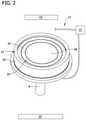
- FIG. 2is a perspective view of the apparatus of FIG. 1 with a portion of a chamber removed for clarity;
- FIG. 3is a cross-section view of a substrate holder of one embodiment of the present disclosure.
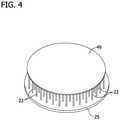
- FIG. 4is a perspective view of the substrate holder of FIG. 3 ;
- FIG. 5is a cross-section view of a substrate holder of a second embodiment of the present disclosure.
- FIG. 6is a perspective view of a tubular pin used in the substrate holder of FIG. 5 ;
- FIG. 7is a cross-section view of a second embodiment of an apparatus for stressing a semiconductor substrate
- FIG. 8is a partial cross-section view of the substrate holder of the apparatus shown in FIG. 7 ;
- FIG. 9is a partial cross-section view of the substrate holder showing a coating on the peripheral edge of the substrate
- FIG. 10is a cross-section view of a third embodiment of an apparatus for stressing a semiconductor substrate
- FIG. 11is a partial cross-section view of the substrate holder of the apparatus shown in FIG. 10 ;
- FIG. 12is a partial cross-section view of the substrate holder illustrating movement of the substrate and top ring upon application of the holder by arrows;
- FIG. 13is a partial cross-section view of a fourth embodiment of an apparatus for stressing a semiconductor substrate
- FIG. 14is a cross-section view of a fifth embodiment of an apparatus for stressing a semiconductor substrate
- FIG. 15is a cross-section view of a sixth embodiment of an apparatus for stressing a semiconductor substrate
- FIG. 16is a cross-section view of the substrate holder of the apparatus shown in FIG. 15 ;
- FIG. 17is a cross-section view of the apparatus
- FIG. 18is a cross-section view of the substrate holder of FIG. 18 indicating stretching of the substrate by an arrow;
- FIG. 19is a partial cross-section view of a third embodiment of a substrate holder
- FIG. 20is a partial cross-section view of an apparatus with the substrate support of FIG. 19 ;
- FIG. 21is a partial cross-section view of the substrate holder of FIG. 19 ;
- FIG. 22is a partial cross-section view of a fourth embodiment of a substrate holder
- FIG. 23is a partial cross-section view of an apparatus with the substrate support of FIG. 22 ;
- FIG. 24is a cross-section view of the substrate holder of FIG. 23 illustrating the direction of application of the front and back support by arrows;
- FIG. 25is a cross-section view of another a fifth of a substrate holder
- FIG. 26is a cross-section view of a sixth embodiment of a substrate holder
- FIG. 27is a cross-section view of a seventh embodiment of a substrate holder
- FIG. 28is a cross-section view of a seventh embodiment of an apparatus for stressing a semiconductor substrate
- FIG. 29is a cross-section view of an eighth embodiment of a substrate holder
- FIG. 30is a bottom view of a substrate holder of a tenth embodiment of a substrate holder
- FIG. 31is a cross-section view of the substrate holder of FIG. 31 ;
- FIG. 32is a cross-section view of the substrate holder mounted to a mounting block support
- FIG. 33is a cross-section view of the substrate holder and mounting block support with a substrate loaded thereon;
- FIG. 34is a cross-section view of the substrate holder and mounting block support with a substrate in a stressed position.
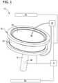
- the apparatus 11may include a chamber 31 and a substrate holder 20 having a substrate support 47 for supporting a semiconductor substrate 49 .
- the illustrated apparatus 11is a single substrate processing apparatus; however, the apparatus and methods disclosed herein are suitable for use in other apparatus including, for example, multiple substrate processing apparatus.
- the apparatusmay also include a “stressor” for stressing the substrate.
- the stressor or stressor assemblymay include one or more heaters 15 or a pressure modulator 27 .
- the heater 15may stress the substrate by causing the substrate to expand at a rate different than the substrate holder (or a portion of the holder) as described below.
- the stressormay be pressure modulator 27 that imparts a differential pressure across the substrate.
- the apparatus 11includes a chamber 31 having an interior space defined in part by walls 33 .
- a perspective of the chamber 31is shown in FIG. 2 with portions of the chamber walls removed to better illustrate the apparatus 11 .
- a substrate holder 20to support a semiconductor substrate 49 .
- the holder 20 illustrated in FIGS. 1-2is a susceptor 47 but other holder arrangements (e.g., tubes, rings, clamps and the like) are contemplated, some of which are more fully described below.
- the substrate holderis designated as 20 in FIGS. 1-2 and as 20 plus a multiple of 100 ( 120 , 220 , 320 etc.) in FIG. 3-34 ).
- the chamber 31may rest on a shaft 9 or other suitable support.
- the apparatus 11such as the shaft 9 , may include devices for causing the holder to grasp and/or release the substrate 49 , such as suitable control valves and/or hydraulic or pneumatic lines or tensioning cables and the like.
- the chamber 31may include other arrangements than those shown herein without departing from the scope of the present disclosure.
- the substrate holder or portions of the holdermay be generally opaque to absorb radiant heating light produced by heaters 15 such as high intensity radiant heating lamps that may be located above and below the chamber 31 .
- the holdermay be constructed of opaque graphite coated with silicon carbide.
- the walls of the chamber 31may be made of a transparent material to allow radiant heating light to pass into the chamber.
- the walls of the chamber 31may be made of transparent quartz. Quartz is generally transparent to infrared and visible light and is chemically stable under typical processing temperatures.
- Heaters 15 other than high intensity lampsmay be used to provide heat to the chamber 31 such as, for example, resistance heaters and inductive heaters.
- the heaters 15may be included within the interior space of the chamber 31 or may be integral with the chamber walls without departing from the scope of the present disclosure.
- the heater or heatersmay be of any suitable type, size and shape, and may be disposed inside or outside the chamber.
- An infrared temperature sensor(not shown) such as a pyrometer may be mounted on the chamber 31 to monitor the temperature of the holder 20 or substrate 49 by receiving infrared radiation emitted by the holder or substrate.
- a system controller 5FIG.
- FIGS. 1-2may be used to control various operating parameters associated with the chamber 31 including, for example, stressor control, gas flow rates and chamber temperature and pressure. It should be understood that apparatus and chamber designs other than that shown in FIGS. 1-2 may be utilized without departing from the scope of the present disclosure.
- the apparatus 11may be configured for and/or include structure suitable for applying a stress to a semiconductor substrate and, optionally, for depositing a semiconductor material such as an epitaxial layer on the substrate.
- a process gas that includes the semiconductor materialmay flow into the apparatus 11 from a source of process gas, such as a gas cylinder, to a gas manifold (not shown) and into the chamber 31 . Gas may be introduced to the chamber 31 before, throughout or after processing. The gas may be heated prior to contacting the substrate 49 .
- the process for depositing an epitaxial layer on a surface of the semiconductor substratemay include methods known in the art and as, for example, as described in U.S. Pat. Nos.
- substrate holders and stressorse.g., heater, pressure modulators and the like
- substrate holders and stressorse.g., heater, pressure modulators and the like
- the holders and stressorsmay be utilized as a part of the apparatus 11 and chamber 31 described above and may be used in combination with a heater for heating the chamber.
- a substrate holder 20may include a number of spaced-apart elongate pins 22 that support the semiconductor substrate 49 .
- the pins 22are attached to a mounting block 25 .
- a forcemay be applied to the substrate 49 to cause the substrate to move (e.g., bend) and contact the pins.
- the pins 22or the upper portions thereof, may collectively define a support surface that is disposed for contacting the substrate 49 in the bent (i.e., stressed) position.
- the pins 22may be arranged in a concave pattern such that upon application of a sufficient force, the substrate 22 deforms or bends from its substantially planar shape to conform to the concave arrangement of the pins. By deforming in this manner, the substrate 22 is stressed.
- the apparatusincludes a pressure modulator as shown in FIG. 1 (and FIG. 7 below) to create a pressure differential across the substrate that is sufficient to exert stress on the substrate.
- a pressure modulatoras shown in FIG. 1 (and FIG. 7 below) to create a pressure differential across the substrate that is sufficient to exert stress on the substrate.
- Other stressorsmay be used in these embodiments.
- pins 22 ′may be tubular, thereby defining a lumen for fluid flow.
- the pins 22 ′are fluidly connected to a pressure modulator 27 such as a pump for pulling a vacuum.
- the vacuum applied to the substrate 49may pull the substrate toward the pins by a pulling force.
- variation in distance between the pins and substrate via a concave pattern of the pinsmay cause different amounts of pulling force to be applied to portions of the substrate. These differential forces cause stress to be applied to the semiconductor substrate 49 .
- the pins 22 , 22 ′generally support the substrate in the vertical direction but may be configured so that they do not restrict movement of the substrate in horizontal or radial directions. Allowing radial movement of the substrate during heating allows the substrate to expand radially without causing slip and dislocations.
- the pinsmay extend through (rather than from) a mounting block and be connected through a series of conduits as described below and shown in FIGS. 31-35 .
- the apparatusin one embodiment of an apparatus for bending a semiconductor substrate, includes a substrate holder 120 having a front ring 131 and a back ring 132 .
- the front ring 131includes an annular front support 134 and the back ring 132 includes an annular back support 136 for contacting and supporting the substrate 49 .
- the front and back ringsmay have an L-shaped cross-section as shown in FIG. 8 .
- the front ring 131is generally adapted to contact the front surface of the substrate 49 at a discrete radial position and the back ring 132 is generally adapted to contact the back surface of the substrate 49 at a discrete radial position.
- the radial positionis slightly inward from the substrate edge.
- the radial position at which the front annular support 134 and back annular support 136 contact the substrate 49may be the same as illustrated in FIG. 8 or may be different without departing from the scope of the present disclosure.
- the apparatus for bending the substrate 49may include a pressure modulator 27 such as a pump to cause a differential pressure across the substrate.
- a pressure modulator 27such as a pump to cause a differential pressure across the substrate.
- pressureis higher on one side of the wafer than the other.
- This differential pressurestresses the substrate and may bend the substrate.
- the front ring 131 and back ring 132act as a seal such that the differential pressure across the substrate 49 may be maintained.
- the pressure modulator 27may be in fluid communication with a vent 3 that extends through the wall of the chamber 31 to a sealed cavity 4 within the chamber.
- the differential pressure applied across the substrate 49may cause the substrate to bend in the direction of lower pressure.
- a protective coating 137covers a portion of the substrate 49 and, in particular, covers the peripheral edges of the substrate.
- the coating 137may generally be any protective material that protects the wafer from damage (such as slip and dislocations) while the substrate is held between the rings 131 , 132 .
- a front ring 131 ′ and back ring 132 ′ of the holder 120 ′may be arranged such that the rings contact the substrate 49 near but not at the peripheral edge of the substrate as with the rings 130 , 131 of apparatus 120 ( FIG. 8 ).
- the rings 131 ′, 132 ′may be integral with the lid and/or bottom of the chamber 31 ′.
- Vents 3 ′may extend through the rings 131 ′, 132 ′ of the chamber 31 ′.
- the vents 3 ′may be located near the center of the substrate 49 and may limit the deflection of the substrate upon activation of the pressure modulator 27 .
- the holder 120 ′may also include a planar support 126 that supports the substrate 49 such as before application of the rings 131 ′, 132 ′.
- the substrate 49is attached to the planar support 126 .
- the planar supportmay be made of a material that has a different thermal expansion coefficient than the substrate (i.e., the rings thermally expand at a different rate than the substrate) to cause the substrate to compress or stretch when the support and substrate are heated or cooled.
- the apparatusexerts stress on the substrate 49 by use of the thermal expansion of the substrate.
- the substrate holder 220may include a clamp 240 including a front ring 231 and a back ring 232 that exerts a holding force on the substrate 49 .
- the front ring 231includes an annular front support 234 and the back ring 232 includes an annular back support 236 .
- the supports 234 , 236contact the substrate 49 at the peripheral edge of the substrate and are adapted to contact the front and back of the substrate respectively.
- the substrate holder 220 illustrated in FIG. 14may be used without a pressure modulator.
- the rings, supports, bosses, clamps and the like of the various holders described hereinmay also be moved radially by any mechanical method including use of pneumatics, hydraulics, motors and the like.
- the rings 231 , 232may be constructed of a material that has a different thermal expansion coefficient than the substrate (i.e., the rings thermally expand at a different rate than the substrate).
- the holding force of the clamp 240 in combination with the differential expansion rates of the rings 231 , 232 upon heating or coolingcauses stress in the substrate 49 .
- the rings 231 , 232have a larger expansion coefficient than the substrate 49
- the ringscause the substrate to stretch radially.
- the substrateexerts an inward force on the substrate (i.e., compression of the substrate) which results in bending of the substrate.
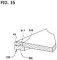
- a substrate holder 320includes a generally planar back support 346 that includes an annular boss 347 that is sized and shaped to be received in a groove 348 in the back of the substrate 49 .
- the boss 347is movable such that it exerts stress on the substrate 49 .
- the back support 346may be made of a material that expands at a lesser rate than that of the substrate 49 upon heating causing compression of the substrate.
- the back support 346may be made of a material that expands at a greater rate than that of the substrate 49 upon heating causing stretching of the substrate.
- the substrate holder 320may also include a front ring and back ring (not shown) with annular supports similar to the front ring 131 and back ring 132 shown in FIG. 8 for sealing of the substrate and allowing a pressure modulator to create a pressure differential across the substrate to stress the substrate.
- the chamber 31 that contains the holder 320may include a vent 3 and sealed cavity 4 for application of a vacuum or pressure ( FIG. 17 ).
- the back ringmay be interior to the back support 346 and the front ring may be aligned with the back ring or may be sized and shaped to be closer to the peripheral edge of the substrate than the back ring.
- the substratemay include a coating as shown in FIG. 9 .
- the substrate holder 320also includes a front support 350 having an annular ring 352 that extends from the front support.
- the ring 352exerts a downward force on the substrate 49 to prevent the substrate from dislodging from the boss 347 during compression or expansion of the substrate during heating.
- Other structures for accomplishing this functionare contemplated within the scope of this disclosure.
- the substrate holder 420includes a back support 446 and boss 447 similar or identical to that shown in FIGS. 15-21 .
- the substrate holder 420also includes a front support 451 and a front boss 455 that is sized and shaped to be received in a groove 457 in the front surface of the substrate 49 .
- the front support 451may also be made of a material that expands at a lesser rate than that of the substrate 49 upon heating causing compression of the substrate or may be made of a material that expands at a greater rate than that of the substrate 49 upon heating causing stretching of the substrate.
- stressing apparatus 520 of this embodimentincludes a planar back support 561 for supporting the substrate 49 and a generally circular press 560 with a circular opening for receiving and compressing the substrate.
- the planar supportmay extend only partially toward the center of the substrate as in FIGS. 26-28 or may extend continuously beneath the substrate 49 .
- the press 560may continuously encircle the substrate or, as shown in FIG. 27 , may include a plurality of arc-shaped segments 563 that form the opening for receiving the substrate 49 .
- the press 560 and/or segments 563may be movable inward relative to the substrate 49 to compress the substrate.
- the press 560may be moved as a result of being composed of a material that expands at a lesser rate than that of the substrate 49 such that the press will compress the substrate upon application of heat.
- the substrate holder 520may also include front and/or back rings (not shown) to form a seal upon use of a pressure modulator for creating a pressure differential across the substrate as described above.
- the substrate holder 620includes a first concave-shaped support 670 and a second concave-shaped support 675 opposite the first concave-shaped support.
- the first concave-shaped support 670includes a plurality of holes 671 formed therein for pulling a vacuum through the holes and for pulling the substrate 49 toward the first concave-shaped support.
- An upper portion 677 of the first support 670contacts a portion of the substrate 49 in its unbent position.
- a lower portion 678that is generally larger than the upper portion and which contains the holes 671 for pulling a vacuum contacts the substrate when it is in its bent position.
- a vent 679is formed in the second support 675 and the support forms a cavity 672 to allow a vacuum to be pulled through the vent and cavity to stress the substrate.
- the annular support 675generally only contacts the substrate 49 near or at the peripheral edge of the substrate.
- a substrate holder 720includes a generally planar back support 781 and a flange 783 .
- the substrate 49includes a ring 780 attached to the back surface of the substrate near the peripheral edge of the substrate.
- the flange 783is adapted to engage the ring 780 .
- the support 781 and flange 783are movable relative to the substrate to compress the substrate. For instance, the support 781 and/or flange 783 may be moved as a result of being composed of a material that expands at a greater rate than that of the substrate 49 such that the flange 783 will stretch the substrate upon application of heat.
- the support 781 and/or flange 783may be moved as a result of being composed of a material that expands at a lesser rate than that of the substrate 49 such that the flange 783 will compress the substrate upon application of heat.
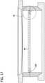
- FIG. 30illustrates the bottom of a mounting block 991 of a substrate holder 920 .
- a series of tubes 989extend through the mounting block 991 to a concave-shaped support 992 ( FIG. 32 ).
- the tubes 989are connected via a series of conduits 990 .
- the mounting block 991may include a handling groove 993 for inserting and removing the mounting block from the processing chamber 31 ( FIG. 1 ).
- the mounting block 991may be supported on a mounting block support 994 within the chamber.
- a vacuum tube 996extends through the mounting block support 994 and is in fluid communication with the conduits 990 and tubes 989 upon insertion of the mounting block into the chamber 31 ( FIG. 1 ).
- a substrate 49is placed on the mounting block 991 ( FIG. 33 ). Upon application of vacuum, the substrate 49 bends toward the concave-shaped support 992 causing stress in the substrate ( FIG. 34 ).
- the stress on the substratemay be directed perpendicular to the axis of the substrate, either by compressing or stretching by use of the embodiments of the apparatus shown in, for example, FIGS. 14-27 and 29 .
- the stressmay be directed along or parallel to the axis of the substrate, such as by use of the embodiments of the apparatus shown in, for example, FIGS. 5, 7-13, 28 and 30-34 .
Landscapes
- Engineering & Computer Science (AREA)
- Physics & Mathematics (AREA)
- Condensed Matter Physics & Semiconductors (AREA)
- General Physics & Mathematics (AREA)
- Manufacturing & Machinery (AREA)
- Computer Hardware Design (AREA)
- Microelectronics & Electronic Packaging (AREA)
- Power Engineering (AREA)
- Chemical & Material Sciences (AREA)
- General Chemical & Material Sciences (AREA)
- Chemical Kinetics & Catalysis (AREA)
- Crystallography & Structural Chemistry (AREA)
- Materials Engineering (AREA)
- Metallurgy (AREA)
- Organic Chemistry (AREA)
- Recrystallisation Techniques (AREA)
- Container, Conveyance, Adherence, Positioning, Of Wafer (AREA)
- Crystals, And After-Treatments Of Crystals (AREA)
- Chemical Vapour Deposition (AREA)
- Semiconductor Lasers (AREA)
Abstract
Description
Claims (13)
Priority Applications (1)
| Application Number | Priority Date | Filing Date | Title |
|---|---|---|---|
| US16/438,003US11276583B2 (en) | 2012-12-31 | 2019-06-11 | Apparatus for stressing semiconductor substrates |
Applications Claiming Priority (6)
| Application Number | Priority Date | Filing Date | Title |
|---|---|---|---|
| US201261747613P | 2012-12-31 | 2012-12-31 | |
| US201361788744P | 2013-03-15 | 2013-03-15 | |
| US201361790445P | 2013-03-15 | 2013-03-15 | |
| US201361793999P | 2013-03-15 | 2013-03-15 | |
| US14/142,559US10361097B2 (en) | 2012-12-31 | 2013-12-27 | Apparatus for stressing semiconductor substrates |
| US16/438,003US11276583B2 (en) | 2012-12-31 | 2019-06-11 | Apparatus for stressing semiconductor substrates |
Related Parent Applications (1)
| Application Number | Title | Priority Date | Filing Date |
|---|---|---|---|
| US14/142,559DivisionUS10361097B2 (en) | 2012-12-31 | 2013-12-27 | Apparatus for stressing semiconductor substrates |
Publications (2)
| Publication Number | Publication Date |
|---|---|
| US20190311913A1 US20190311913A1 (en) | 2019-10-10 |
| US11276583B2true US11276583B2 (en) | 2022-03-15 |
Family
ID=49958756
Family Applications (7)
| Application Number | Title | Priority Date | Filing Date |
|---|---|---|---|
| US14/142,553Active2035-02-25US9583363B2 (en) | 2012-12-31 | 2013-12-27 | Processes and apparatus for preparing heterostructures with reduced strain by radial distension |
| US14/142,559ActiveUS10361097B2 (en) | 2012-12-31 | 2013-12-27 | Apparatus for stressing semiconductor substrates |
| US14/142,556Active2035-01-09US9583364B2 (en) | 2012-12-31 | 2013-12-27 | Processes and apparatus for preparing heterostructures with reduced strain by radial compression |
| US16/437,996ActiveUS11282715B2 (en) | 2012-12-31 | 2019-06-11 | Apparatus for stressing semiconductor substrates |
| US16/438,003ActiveUS11276583B2 (en) | 2012-12-31 | 2019-06-11 | Apparatus for stressing semiconductor substrates |
| US16/438,000ActiveUS11276582B2 (en) | 2012-12-31 | 2019-06-11 | Apparatus for stressing semiconductor substrates |
| US16/437,988Active2034-03-23US11764071B2 (en) | 2012-12-31 | 2019-06-11 | Apparatus for stressing semiconductor substrates |
Family Applications Before (4)
| Application Number | Title | Priority Date | Filing Date |
|---|---|---|---|
| US14/142,553Active2035-02-25US9583363B2 (en) | 2012-12-31 | 2013-12-27 | Processes and apparatus for preparing heterostructures with reduced strain by radial distension |
| US14/142,559ActiveUS10361097B2 (en) | 2012-12-31 | 2013-12-27 | Apparatus for stressing semiconductor substrates |
| US14/142,556Active2035-01-09US9583364B2 (en) | 2012-12-31 | 2013-12-27 | Processes and apparatus for preparing heterostructures with reduced strain by radial compression |
| US16/437,996ActiveUS11282715B2 (en) | 2012-12-31 | 2019-06-11 | Apparatus for stressing semiconductor substrates |
Family Applications After (2)
| Application Number | Title | Priority Date | Filing Date |
|---|---|---|---|
| US16/438,000ActiveUS11276582B2 (en) | 2012-12-31 | 2019-06-11 | Apparatus for stressing semiconductor substrates |
| US16/437,988Active2034-03-23US11764071B2 (en) | 2012-12-31 | 2019-06-11 | Apparatus for stressing semiconductor substrates |
Country Status (7)
| Country | Link |
|---|---|
| US (7) | US9583363B2 (en) |
| EP (6) | EP3188224B1 (en) |
| JP (10) | JP6314153B2 (en) |
| KR (2) | KR102203560B1 (en) |
| CN (5) | CN107968067B (en) |
| TW (4) | TWI673865B (en) |
| WO (3) | WO2014106177A1 (en) |
Cited By (1)
| Publication number | Priority date | Publication date | Assignee | Title |
|---|---|---|---|---|
| US20190333778A1 (en)* | 2012-12-31 | 2019-10-31 | Globalwafers Co., Ltd. | Apparatus for stressing semiconductor substrates |
Families Citing this family (265)
| Publication number | Priority date | Publication date | Assignee | Title |
|---|---|---|---|---|
| US20130023129A1 (en) | 2011-07-20 | 2013-01-24 | Asm America, Inc. | Pressure transmitter for a semiconductor processing environment |
| US10714315B2 (en) | 2012-10-12 | 2020-07-14 | Asm Ip Holdings B.V. | Semiconductor reaction chamber showerhead |
| US20160376700A1 (en) | 2013-02-01 | 2016-12-29 | Asm Ip Holding B.V. | System for treatment of deposition reactor |
| WO2014191624A1 (en)* | 2013-05-29 | 2014-12-04 | Beneq Oy | Substrate holder and arrangement for holding substrates |
| WO2014191621A1 (en)* | 2013-05-29 | 2014-12-04 | Beneq Oy | Substrate carrier and arrangement for supporting substrates |
| US10941490B2 (en) | 2014-10-07 | 2021-03-09 | Asm Ip Holding B.V. | Multiple temperature range susceptor, assembly, reactor and system including the susceptor, and methods of using the same |
| US10276355B2 (en) | 2015-03-12 | 2019-04-30 | Asm Ip Holding B.V. | Multi-zone reactor, system including the reactor, and method of using the same |
| US10458018B2 (en) | 2015-06-26 | 2019-10-29 | Asm Ip Holding B.V. | Structures including metal carbide material, devices including the structures, and methods of forming same |
| US10211308B2 (en) | 2015-10-21 | 2019-02-19 | Asm Ip Holding B.V. | NbMC layers |
| DE102015223807A1 (en)* | 2015-12-01 | 2017-06-01 | Siltronic Ag | Process for producing a semiconductor wafer with epitaxial layer in a deposition chamber, apparatus for producing an epitaxial-layer semiconductor wafer and semiconductor wafer with epitaxial layer |
| US11139308B2 (en) | 2015-12-29 | 2021-10-05 | Asm Ip Holding B.V. | Atomic layer deposition of III-V compounds to form V-NAND devices |
| US10529554B2 (en) | 2016-02-19 | 2020-01-07 | Asm Ip Holding B.V. | Method for forming silicon nitride film selectively on sidewalls or flat surfaces of trenches |
| US10343920B2 (en) | 2016-03-18 | 2019-07-09 | Asm Ip Holding B.V. | Aligned carbon nanotubes |
| US11453943B2 (en) | 2016-05-25 | 2022-09-27 | Asm Ip Holding B.V. | Method for forming carbon-containing silicon/metal oxide or nitride film by ALD using silicon precursor and hydrocarbon precursor |
| US10612137B2 (en) | 2016-07-08 | 2020-04-07 | Asm Ip Holdings B.V. | Organic reactants for atomic layer deposition |
| US9859151B1 (en) | 2016-07-08 | 2018-01-02 | Asm Ip Holding B.V. | Selective film deposition method to form air gaps |
| CN107623028B (en)* | 2016-07-13 | 2021-02-19 | 环球晶圆股份有限公司 | Semiconductor substrate and processing method thereof |
| US9887082B1 (en) | 2016-07-28 | 2018-02-06 | Asm Ip Holding B.V. | Method and apparatus for filling a gap |
| US9812320B1 (en) | 2016-07-28 | 2017-11-07 | Asm Ip Holding B.V. | Method and apparatus for filling a gap |
| CN109564868B (en)* | 2016-08-25 | 2023-04-04 | 日本瑞翁株式会社 | Plasma etching method |
| US11532757B2 (en) | 2016-10-27 | 2022-12-20 | Asm Ip Holding B.V. | Deposition of charge trapping layers |
| US10714350B2 (en) | 2016-11-01 | 2020-07-14 | ASM IP Holdings, B.V. | Methods for forming a transition metal niobium nitride film on a substrate by atomic layer deposition and related semiconductor device structures |
| KR102546317B1 (en) | 2016-11-15 | 2023-06-21 | 에이에스엠 아이피 홀딩 비.브이. | Gas supply unit and substrate processing apparatus including the same |
| KR102762543B1 (en) | 2016-12-14 | 2025-02-05 | 에이에스엠 아이피 홀딩 비.브이. | Substrate processing apparatus |
| US11581186B2 (en) | 2016-12-15 | 2023-02-14 | Asm Ip Holding B.V. | Sequential infiltration synthesis apparatus |
| US11447861B2 (en) | 2016-12-15 | 2022-09-20 | Asm Ip Holding B.V. | Sequential infiltration synthesis apparatus and a method of forming a patterned structure |
| US10269558B2 (en) | 2016-12-22 | 2019-04-23 | Asm Ip Holding B.V. | Method of forming a structure on a substrate |
| US10068787B2 (en)* | 2016-12-30 | 2018-09-04 | Sunpower Corporation | Bowing semiconductor wafers |
| US11390950B2 (en) | 2017-01-10 | 2022-07-19 | Asm Ip Holding B.V. | Reactor system and method to reduce residue buildup during a film deposition process |
| US10468261B2 (en) | 2017-02-15 | 2019-11-05 | Asm Ip Holding B.V. | Methods for forming a metallic film on a substrate by cyclical deposition and related semiconductor device structures |
| US10770286B2 (en) | 2017-05-08 | 2020-09-08 | Asm Ip Holdings B.V. | Methods for selectively forming a silicon nitride film on a substrate and related semiconductor device structures |
| KR102015336B1 (en)* | 2017-06-12 | 2019-08-28 | 삼성전자주식회사 | Method of reducing warpage of semiconductor package substrate and warpage reducer device |
| US12040200B2 (en) | 2017-06-20 | 2024-07-16 | Asm Ip Holding B.V. | Semiconductor processing apparatus and methods for calibrating a semiconductor processing apparatus |
| US11306395B2 (en) | 2017-06-28 | 2022-04-19 | Asm Ip Holding B.V. | Methods for depositing a transition metal nitride film on a substrate by atomic layer deposition and related deposition apparatus |
| KR20190009245A (en) | 2017-07-18 | 2019-01-28 | 에이에스엠 아이피 홀딩 비.브이. | Methods for forming a semiconductor device structure and related semiconductor device structures |
| US11374112B2 (en) | 2017-07-19 | 2022-06-28 | Asm Ip Holding B.V. | Method for depositing a group IV semiconductor and related semiconductor device structures |
| US10590535B2 (en) | 2017-07-26 | 2020-03-17 | Asm Ip Holdings B.V. | Chemical treatment, deposition and/or infiltration apparatus and method for using the same |
| TWI815813B (en) | 2017-08-04 | 2023-09-21 | 荷蘭商Asm智慧財產控股公司 | Showerhead assembly for distributing a gas within a reaction chamber |
| US10692741B2 (en) | 2017-08-08 | 2020-06-23 | Asm Ip Holdings B.V. | Radiation shield |
| US10770336B2 (en) | 2017-08-08 | 2020-09-08 | Asm Ip Holding B.V. | Substrate lift mechanism and reactor including same |
| US11769682B2 (en) | 2017-08-09 | 2023-09-26 | Asm Ip Holding B.V. | Storage apparatus for storing cassettes for substrates and processing apparatus equipped therewith |
| US11830730B2 (en) | 2017-08-29 | 2023-11-28 | Asm Ip Holding B.V. | Layer forming method and apparatus |
| US11295980B2 (en) | 2017-08-30 | 2022-04-05 | Asm Ip Holding B.V. | Methods for depositing a molybdenum metal film over a dielectric surface of a substrate by a cyclical deposition process and related semiconductor device structures |
| US10658205B2 (en) | 2017-09-28 | 2020-05-19 | Asm Ip Holdings B.V. | Chemical dispensing apparatus and methods for dispensing a chemical to a reaction chamber |
| US10403504B2 (en) | 2017-10-05 | 2019-09-03 | Asm Ip Holding B.V. | Method for selectively depositing a metallic film on a substrate |
| US10923344B2 (en) | 2017-10-30 | 2021-02-16 | Asm Ip Holding B.V. | Methods for forming a semiconductor structure and related semiconductor structures |
| WO2019103613A1 (en) | 2017-11-27 | 2019-05-31 | Asm Ip Holding B.V. | A storage device for storing wafer cassettes for use with a batch furnace |
| CN111344522B (en) | 2017-11-27 | 2022-04-12 | 阿斯莫Ip控股公司 | Including clean mini-environment device |
| US10872771B2 (en) | 2018-01-16 | 2020-12-22 | Asm Ip Holding B. V. | Method for depositing a material film on a substrate within a reaction chamber by a cyclical deposition process and related device structures |
| TWI799494B (en) | 2018-01-19 | 2023-04-21 | 荷蘭商Asm 智慧財產控股公司 | Deposition method |
| KR102695659B1 (en) | 2018-01-19 | 2024-08-14 | 에이에스엠 아이피 홀딩 비.브이. | Method for depositing a gap filling layer by plasma assisted deposition |
| US11081345B2 (en) | 2018-02-06 | 2021-08-03 | Asm Ip Holding B.V. | Method of post-deposition treatment for silicon oxide film |
| US10896820B2 (en) | 2018-02-14 | 2021-01-19 | Asm Ip Holding B.V. | Method for depositing a ruthenium-containing film on a substrate by a cyclical deposition process |
| WO2019158960A1 (en) | 2018-02-14 | 2019-08-22 | Asm Ip Holding B.V. | A method for depositing a ruthenium-containing film on a substrate by a cyclical deposition process |
| US10731249B2 (en) | 2018-02-15 | 2020-08-04 | Asm Ip Holding B.V. | Method of forming a transition metal containing film on a substrate by a cyclical deposition process, a method for supplying a transition metal halide compound to a reaction chamber, and related vapor deposition apparatus |
| KR102636427B1 (en) | 2018-02-20 | 2024-02-13 | 에이에스엠 아이피 홀딩 비.브이. | Substrate processing method and apparatus |
| US10975470B2 (en) | 2018-02-23 | 2021-04-13 | Asm Ip Holding B.V. | Apparatus for detecting or monitoring for a chemical precursor in a high temperature environment |
| US11473195B2 (en) | 2018-03-01 | 2022-10-18 | Asm Ip Holding B.V. | Semiconductor processing apparatus and a method for processing a substrate |
| US11629406B2 (en) | 2018-03-09 | 2023-04-18 | Asm Ip Holding B.V. | Semiconductor processing apparatus comprising one or more pyrometers for measuring a temperature of a substrate during transfer of the substrate |
| KR102646467B1 (en) | 2018-03-27 | 2024-03-11 | 에이에스엠 아이피 홀딩 비.브이. | Method of forming an electrode on a substrate and a semiconductor device structure including an electrode |
| US11230766B2 (en) | 2018-03-29 | 2022-01-25 | Asm Ip Holding B.V. | Substrate processing apparatus and method |
| KR102600229B1 (en) | 2018-04-09 | 2023-11-10 | 에이에스엠 아이피 홀딩 비.브이. | Substrate supporting device, substrate processing apparatus including the same and substrate processing method |
| US12025484B2 (en) | 2018-05-08 | 2024-07-02 | Asm Ip Holding B.V. | Thin film forming method |
| TWI811348B (en) | 2018-05-08 | 2023-08-11 | 荷蘭商Asm 智慧財產控股公司 | Methods for depositing an oxide film on a substrate by a cyclical deposition process and related device structures |
| US12272527B2 (en) | 2018-05-09 | 2025-04-08 | Asm Ip Holding B.V. | Apparatus for use with hydrogen radicals and method of using same |
| KR102596988B1 (en) | 2018-05-28 | 2023-10-31 | 에이에스엠 아이피 홀딩 비.브이. | Method of processing a substrate and a device manufactured by the same |
| US11201079B2 (en)* | 2018-05-30 | 2021-12-14 | Taiwan Semiconductor Manufacturing Company, Ltd. | Wafer chuck |
| US11718913B2 (en) | 2018-06-04 | 2023-08-08 | Asm Ip Holding B.V. | Gas distribution system and reactor system including same |
| TWI840362B (en) | 2018-06-04 | 2024-05-01 | 荷蘭商Asm Ip私人控股有限公司 | Wafer handling chamber with moisture reduction |
| US11286562B2 (en) | 2018-06-08 | 2022-03-29 | Asm Ip Holding B.V. | Gas-phase chemical reactor and method of using same |
| KR102568797B1 (en) | 2018-06-21 | 2023-08-21 | 에이에스엠 아이피 홀딩 비.브이. | Substrate processing system |
| US10797133B2 (en) | 2018-06-21 | 2020-10-06 | Asm Ip Holding B.V. | Method for depositing a phosphorus doped silicon arsenide film and related semiconductor device structures |
| KR102854019B1 (en) | 2018-06-27 | 2025-09-02 | 에이에스엠 아이피 홀딩 비.브이. | Periodic deposition method for forming a metal-containing material and films and structures comprising the metal-containing material |
| TWI873894B (en) | 2018-06-27 | 2025-02-21 | 荷蘭商Asm Ip私人控股有限公司 | Cyclic deposition methods for forming metal-containing material and films and structures including the metal-containing material |
| US10612136B2 (en) | 2018-06-29 | 2020-04-07 | ASM IP Holding, B.V. | Temperature-controlled flange and reactor system including same |
| US10755922B2 (en) | 2018-07-03 | 2020-08-25 | Asm Ip Holding B.V. | Method for depositing silicon-free carbon-containing film as gap-fill layer by pulse plasma-assisted deposition |
| US10388513B1 (en) | 2018-07-03 | 2019-08-20 | Asm Ip Holding B.V. | Method for depositing silicon-free carbon-containing film as gap-fill layer by pulse plasma-assisted deposition |
| US11430674B2 (en) | 2018-08-22 | 2022-08-30 | Asm Ip Holding B.V. | Sensor array, apparatus for dispensing a vapor phase reactant to a reaction chamber and related methods |
| US11024523B2 (en) | 2018-09-11 | 2021-06-01 | Asm Ip Holding B.V. | Substrate processing apparatus and method |
| KR102707956B1 (en) | 2018-09-11 | 2024-09-19 | 에이에스엠 아이피 홀딩 비.브이. | Method for deposition of a thin film |
| CN110970344B (en) | 2018-10-01 | 2024-10-25 | Asmip控股有限公司 | Substrate holding apparatus, system comprising the same and method of using the same |
| US11232963B2 (en) | 2018-10-03 | 2022-01-25 | Asm Ip Holding B.V. | Substrate processing apparatus and method |
| KR102592699B1 (en) | 2018-10-08 | 2023-10-23 | 에이에스엠 아이피 홀딩 비.브이. | Substrate support unit and apparatuses for depositing thin film and processing the substrate including the same |
| KR102546322B1 (en) | 2018-10-19 | 2023-06-21 | 에이에스엠 아이피 홀딩 비.브이. | Substrate processing apparatus and substrate processing method |
| KR102605121B1 (en) | 2018-10-19 | 2023-11-23 | 에이에스엠 아이피 홀딩 비.브이. | Substrate processing apparatus and substrate processing method |
| US12378665B2 (en) | 2018-10-26 | 2025-08-05 | Asm Ip Holding B.V. | High temperature coatings for a preclean and etch apparatus and related methods |
| US11087997B2 (en) | 2018-10-31 | 2021-08-10 | Asm Ip Holding B.V. | Substrate processing apparatus for processing substrates |
| KR102748291B1 (en) | 2018-11-02 | 2024-12-31 | 에이에스엠 아이피 홀딩 비.브이. | Substrate support unit and substrate processing apparatus including the same |
| US11572620B2 (en) | 2018-11-06 | 2023-02-07 | Asm Ip Holding B.V. | Methods for selectively depositing an amorphous silicon film on a substrate |
| US10818758B2 (en) | 2018-11-16 | 2020-10-27 | Asm Ip Holding B.V. | Methods for forming a metal silicate film on a substrate in a reaction chamber and related semiconductor device structures |
| US12040199B2 (en) | 2018-11-28 | 2024-07-16 | Asm Ip Holding B.V. | Substrate processing apparatus for processing substrates |
| US11217444B2 (en) | 2018-11-30 | 2022-01-04 | Asm Ip Holding B.V. | Method for forming an ultraviolet radiation responsive metal oxide-containing film |
| KR102636428B1 (en) | 2018-12-04 | 2024-02-13 | 에이에스엠 아이피 홀딩 비.브이. | A method for cleaning a substrate processing apparatus |
| US11158513B2 (en) | 2018-12-13 | 2021-10-26 | Asm Ip Holding B.V. | Methods for forming a rhenium-containing film on a substrate by a cyclical deposition process and related semiconductor device structures |
| TWI874340B (en) | 2018-12-14 | 2025-03-01 | 荷蘭商Asm Ip私人控股有限公司 | Method of forming device structure, structure formed by the method and system for performing the method |
| TWI866480B (en) | 2019-01-17 | 2024-12-11 | 荷蘭商Asm Ip 私人控股有限公司 | Methods of forming a transition metal containing film on a substrate by a cyclical deposition process |
| KR102727227B1 (en) | 2019-01-22 | 2024-11-07 | 에이에스엠 아이피 홀딩 비.브이. | Semiconductor processing device |
| TWI838458B (en)* | 2019-02-20 | 2024-04-11 | 荷蘭商Asm Ip私人控股有限公司 | Apparatus and methods for plug fill deposition in 3-d nand applications |
| TWI845607B (en) | 2019-02-20 | 2024-06-21 | 荷蘭商Asm Ip私人控股有限公司 | Cyclical deposition method and apparatus for filling a recess formed within a substrate surface |
| KR102626263B1 (en) | 2019-02-20 | 2024-01-16 | 에이에스엠 아이피 홀딩 비.브이. | Cyclical deposition method including treatment step and apparatus for same |
| TWI873122B (en) | 2019-02-20 | 2025-02-21 | 荷蘭商Asm Ip私人控股有限公司 | Method of filling a recess formed within a surface of a substrate, semiconductor structure formed according to the method, and semiconductor processing apparatus |
| TWI842826B (en) | 2019-02-22 | 2024-05-21 | 荷蘭商Asm Ip私人控股有限公司 | Substrate processing apparatus and method for processing substrate |
| KR102858005B1 (en) | 2019-03-08 | 2025-09-09 | 에이에스엠 아이피 홀딩 비.브이. | Method for Selective Deposition of Silicon Nitride Layer and Structure Including Selectively-Deposited Silicon Nitride Layer |
| US11742198B2 (en) | 2019-03-08 | 2023-08-29 | Asm Ip Holding B.V. | Structure including SiOCN layer and method of forming same |
| KR102673983B1 (en)* | 2019-03-15 | 2024-06-12 | 주식회사 케이씨텍 | Apparatus for Treating Substrate |
| JP7279465B2 (en)* | 2019-03-28 | 2023-05-23 | 住友金属鉱山株式会社 | SUPPORTING SUBSTRATE, SUPPORTING SUBSTRATE HOLDING METHOD, AND FILM-FORMING METHOD |
| JP2020167398A (en) | 2019-03-28 | 2020-10-08 | エーエスエム・アイピー・ホールディング・ベー・フェー | Door openers and substrate processing equipment provided with door openers |
| KR102809999B1 (en) | 2019-04-01 | 2025-05-19 | 에이에스엠 아이피 홀딩 비.브이. | Method of manufacturing semiconductor device |
| KR20200123380A (en) | 2019-04-19 | 2020-10-29 | 에이에스엠 아이피 홀딩 비.브이. | Layer forming method and apparatus |
| KR20200125453A (en) | 2019-04-24 | 2020-11-04 | 에이에스엠 아이피 홀딩 비.브이. | Gas-phase reactor system and method of using same |
| KR20200130121A (en) | 2019-05-07 | 2020-11-18 | 에이에스엠 아이피 홀딩 비.브이. | Chemical source vessel with dip tube |
| US11289326B2 (en) | 2019-05-07 | 2022-03-29 | Asm Ip Holding B.V. | Method for reforming amorphous carbon polymer film |
| KR20200130652A (en) | 2019-05-10 | 2020-11-19 | 에이에스엠 아이피 홀딩 비.브이. | Method of depositing material onto a surface and structure formed according to the method |
| JP7612342B2 (en) | 2019-05-16 | 2025-01-14 | エーエスエム・アイピー・ホールディング・ベー・フェー | Wafer boat handling apparatus, vertical batch furnace and method |
| JP7598201B2 (en) | 2019-05-16 | 2024-12-11 | エーエスエム・アイピー・ホールディング・ベー・フェー | Wafer boat handling apparatus, vertical batch furnace and method |
| USD975665S1 (en) | 2019-05-17 | 2023-01-17 | Asm Ip Holding B.V. | Susceptor shaft |
| USD947913S1 (en) | 2019-05-17 | 2022-04-05 | Asm Ip Holding B.V. | Susceptor shaft |
| KR20200141002A (en) | 2019-06-06 | 2020-12-17 | 에이에스엠 아이피 홀딩 비.브이. | Method of using a gas-phase reactor system including analyzing exhausted gas |
| KR20200141931A (en) | 2019-06-10 | 2020-12-21 | 에이에스엠 아이피 홀딩 비.브이. | Method for cleaning quartz epitaxial chambers |
| KR20200143254A (en) | 2019-06-11 | 2020-12-23 | 에이에스엠 아이피 홀딩 비.브이. | Method of forming an electronic structure using an reforming gas, system for performing the method, and structure formed using the method |
| USD944946S1 (en) | 2019-06-14 | 2022-03-01 | Asm Ip Holding B.V. | Shower plate |
| KR20210005515A (en) | 2019-07-03 | 2021-01-14 | 에이에스엠 아이피 홀딩 비.브이. | Temperature control assembly for substrate processing apparatus and method of using same |
| JP7499079B2 (en) | 2019-07-09 | 2024-06-13 | エーエスエム・アイピー・ホールディング・ベー・フェー | Plasma device using coaxial waveguide and substrate processing method |
| CN112216646A (en) | 2019-07-10 | 2021-01-12 | Asm Ip私人控股有限公司 | Substrate supporting assembly and substrate processing device comprising same |
| KR20210010307A (en) | 2019-07-16 | 2021-01-27 | 에이에스엠 아이피 홀딩 비.브이. | Substrate processing apparatus |
| KR102860110B1 (en) | 2019-07-17 | 2025-09-16 | 에이에스엠 아이피 홀딩 비.브이. | Methods of forming silicon germanium structures |
| KR20210010816A (en) | 2019-07-17 | 2021-01-28 | 에이에스엠 아이피 홀딩 비.브이. | Radical assist ignition plasma system and method |
| US11643724B2 (en) | 2019-07-18 | 2023-05-09 | Asm Ip Holding B.V. | Method of forming structures using a neutral beam |
| TWI839544B (en) | 2019-07-19 | 2024-04-21 | 荷蘭商Asm Ip私人控股有限公司 | Method of forming topology-controlled amorphous carbon polymer film |
| KR20210010817A (en) | 2019-07-19 | 2021-01-28 | 에이에스엠 아이피 홀딩 비.브이. | Method of Forming Topology-Controlled Amorphous Carbon Polymer Film |
| TWI851767B (en) | 2019-07-29 | 2024-08-11 | 荷蘭商Asm Ip私人控股有限公司 | Methods for selective deposition utilizing n-type dopants and/or alternative dopants to achieve high dopant incorporation |
| CN112309900A (en) | 2019-07-30 | 2021-02-02 | Asm Ip私人控股有限公司 | Substrate processing apparatus |
| CN112309899A (en) | 2019-07-30 | 2021-02-02 | Asm Ip私人控股有限公司 | Substrate processing apparatus |
| US12169361B2 (en) | 2019-07-30 | 2024-12-17 | Asm Ip Holding B.V. | Substrate processing apparatus and method |
| US11587815B2 (en) | 2019-07-31 | 2023-02-21 | Asm Ip Holding B.V. | Vertical batch furnace assembly |
| US11227782B2 (en) | 2019-07-31 | 2022-01-18 | Asm Ip Holding B.V. | Vertical batch furnace assembly |
| US11587814B2 (en) | 2019-07-31 | 2023-02-21 | Asm Ip Holding B.V. | Vertical batch furnace assembly |
| CN112323048B (en) | 2019-08-05 | 2024-02-09 | Asm Ip私人控股有限公司 | Liquid level sensor for chemical source container |
| CN112342526A (en) | 2019-08-09 | 2021-02-09 | Asm Ip私人控股有限公司 | Heater assembly including cooling device and method of using same |
| USD965524S1 (en) | 2019-08-19 | 2022-10-04 | Asm Ip Holding B.V. | Susceptor support |
| USD965044S1 (en) | 2019-08-19 | 2022-09-27 | Asm Ip Holding B.V. | Susceptor shaft |
| JP2021031769A (en) | 2019-08-21 | 2021-03-01 | エーエスエム アイピー ホールディング ビー.ブイ. | Production apparatus of mixed gas of film deposition raw material and film deposition apparatus |
| USD979506S1 (en) | 2019-08-22 | 2023-02-28 | Asm Ip Holding B.V. | Insulator |
| KR20210024423A (en) | 2019-08-22 | 2021-03-05 | 에이에스엠 아이피 홀딩 비.브이. | Method for forming a structure with a hole |
| USD949319S1 (en) | 2019-08-22 | 2022-04-19 | Asm Ip Holding B.V. | Exhaust duct |
| USD940837S1 (en) | 2019-08-22 | 2022-01-11 | Asm Ip Holding B.V. | Electrode |
| KR20210024420A (en) | 2019-08-23 | 2021-03-05 | 에이에스엠 아이피 홀딩 비.브이. | Method for depositing silicon oxide film having improved quality by peald using bis(diethylamino)silane |
| US11286558B2 (en) | 2019-08-23 | 2022-03-29 | Asm Ip Holding B.V. | Methods for depositing a molybdenum nitride film on a surface of a substrate by a cyclical deposition process and related semiconductor device structures including a molybdenum nitride film |
| KR102806450B1 (en) | 2019-09-04 | 2025-05-12 | 에이에스엠 아이피 홀딩 비.브이. | Methods for selective deposition using a sacrificial capping layer |
| KR102733104B1 (en) | 2019-09-05 | 2024-11-22 | 에이에스엠 아이피 홀딩 비.브이. | Substrate processing apparatus |
| US11562901B2 (en) | 2019-09-25 | 2023-01-24 | Asm Ip Holding B.V. | Substrate processing method |
| CN112593212B (en) | 2019-10-02 | 2023-12-22 | Asm Ip私人控股有限公司 | Method for forming topologically selective silicon oxide film by cyclic plasma enhanced deposition process |
| TWI846953B (en) | 2019-10-08 | 2024-07-01 | 荷蘭商Asm Ip私人控股有限公司 | Substrate processing device |
| KR20210042810A (en) | 2019-10-08 | 2021-04-20 | 에이에스엠 아이피 홀딩 비.브이. | Reactor system including a gas distribution assembly for use with activated species and method of using same |
| TW202128273A (en) | 2019-10-08 | 2021-08-01 | 荷蘭商Asm Ip私人控股有限公司 | Gas injection system, reactor system, and method of depositing material on surface of substratewithin reaction chamber |
| TWI846966B (en) | 2019-10-10 | 2024-07-01 | 荷蘭商Asm Ip私人控股有限公司 | Method of forming a photoresist underlayer and structure including same |
| US12009241B2 (en) | 2019-10-14 | 2024-06-11 | Asm Ip Holding B.V. | Vertical batch furnace assembly with detector to detect cassette |
| TWI834919B (en) | 2019-10-16 | 2024-03-11 | 荷蘭商Asm Ip私人控股有限公司 | Method of topology-selective film formation of silicon oxide |
| US11637014B2 (en) | 2019-10-17 | 2023-04-25 | Asm Ip Holding B.V. | Methods for selective deposition of doped semiconductor material |
| KR102845724B1 (en) | 2019-10-21 | 2025-08-13 | 에이에스엠 아이피 홀딩 비.브이. | Apparatus and methods for selectively etching films |
| US11328944B2 (en)* | 2019-10-23 | 2022-05-10 | Eugenus, Inc. | Systems and methods of placing substrates in semiconductor manufacturing equipment |
| KR20210050453A (en) | 2019-10-25 | 2021-05-07 | 에이에스엠 아이피 홀딩 비.브이. | Methods for filling a gap feature on a substrate surface and related semiconductor structures |
| US11646205B2 (en) | 2019-10-29 | 2023-05-09 | Asm Ip Holding B.V. | Methods of selectively forming n-type doped material on a surface, systems for selectively forming n-type doped material, and structures formed using same |
| KR20210054983A (en) | 2019-11-05 | 2021-05-14 | 에이에스엠 아이피 홀딩 비.브이. | Structures with doped semiconductor layers and methods and systems for forming same |
| US11501968B2 (en) | 2019-11-15 | 2022-11-15 | Asm Ip Holding B.V. | Method for providing a semiconductor device with silicon filled gaps |
| KR102861314B1 (en) | 2019-11-20 | 2025-09-17 | 에이에스엠 아이피 홀딩 비.브이. | Method of depositing carbon-containing material on a surface of a substrate, structure formed using the method, and system for forming the structure |
| US11450529B2 (en) | 2019-11-26 | 2022-09-20 | Asm Ip Holding B.V. | Methods for selectively forming a target film on a substrate comprising a first dielectric surface and a second metallic surface |
| CN112951697B (en) | 2019-11-26 | 2025-07-29 | Asmip私人控股有限公司 | Substrate processing apparatus |
| CN112885692B (en) | 2019-11-29 | 2025-08-15 | Asmip私人控股有限公司 | Substrate processing apparatus |
| CN120432376A (en) | 2019-11-29 | 2025-08-05 | Asm Ip私人控股有限公司 | Substrate processing apparatus |
| JP7527928B2 (en) | 2019-12-02 | 2024-08-05 | エーエスエム・アイピー・ホールディング・ベー・フェー | Substrate processing apparatus and substrate processing method |
| KR20210070898A (en) | 2019-12-04 | 2021-06-15 | 에이에스엠 아이피 홀딩 비.브이. | Substrate processing apparatus |
| KR20210078405A (en) | 2019-12-17 | 2021-06-28 | 에이에스엠 아이피 홀딩 비.브이. | Method of forming vanadium nitride layer and structure including the vanadium nitride layer |
| KR20210080214A (en) | 2019-12-19 | 2021-06-30 | 에이에스엠 아이피 홀딩 비.브이. | Methods for filling a gap feature on a substrate and related semiconductor structures |
| JP7730637B2 (en) | 2020-01-06 | 2025-08-28 | エーエスエム・アイピー・ホールディング・ベー・フェー | Gas delivery assembly, components thereof, and reactor system including same |
| JP7636892B2 (en) | 2020-01-06 | 2025-02-27 | エーエスエム・アイピー・ホールディング・ベー・フェー | Channeled Lift Pins |
| US11993847B2 (en) | 2020-01-08 | 2024-05-28 | Asm Ip Holding B.V. | Injector |
| KR20210093163A (en) | 2020-01-16 | 2021-07-27 | 에이에스엠 아이피 홀딩 비.브이. | Method of forming high aspect ratio features |
| US11791192B2 (en)* | 2020-01-19 | 2023-10-17 | Taiwan Semiconductor Manufacturing Company, Ltd. | Workpiece holder, wafer chuck, wafer holding method |
| KR102675856B1 (en) | 2020-01-20 | 2024-06-17 | 에이에스엠 아이피 홀딩 비.브이. | Method of forming thin film and method of modifying surface of thin film |
| TWI889744B (en) | 2020-01-29 | 2025-07-11 | 荷蘭商Asm Ip私人控股有限公司 | Contaminant trap system, and baffle plate stack |
| TW202513845A (en) | 2020-02-03 | 2025-04-01 | 荷蘭商Asm Ip私人控股有限公司 | Semiconductor structures and methods for forming the same |
| KR20210100010A (en) | 2020-02-04 | 2021-08-13 | 에이에스엠 아이피 홀딩 비.브이. | Method and apparatus for transmittance measurements of large articles |
| US11776846B2 (en) | 2020-02-07 | 2023-10-03 | Asm Ip Holding B.V. | Methods for depositing gap filling fluids and related systems and devices |
| KR20210103956A (en) | 2020-02-13 | 2021-08-24 | 에이에스엠 아이피 홀딩 비.브이. | Substrate processing apparatus including light receiving device and calibration method of light receiving device |
| TW202146691A (en) | 2020-02-13 | 2021-12-16 | 荷蘭商Asm Ip私人控股有限公司 | Gas distribution assembly, shower plate assembly, and method of adjusting conductance of gas to reaction chamber |
| TWI855223B (en) | 2020-02-17 | 2024-09-11 | 荷蘭商Asm Ip私人控股有限公司 | Method for growing phosphorous-doped silicon layer |
| CN113410160A (en) | 2020-02-28 | 2021-09-17 | Asm Ip私人控股有限公司 | System specially used for cleaning parts |
| KR20210113043A (en) | 2020-03-04 | 2021-09-15 | 에이에스엠 아이피 홀딩 비.브이. | Alignment fixture for a reactor system |
| US11876356B2 (en) | 2020-03-11 | 2024-01-16 | Asm Ip Holding B.V. | Lockout tagout assembly and system and method of using same |
| KR20210116240A (en) | 2020-03-11 | 2021-09-27 | 에이에스엠 아이피 홀딩 비.브이. | Substrate handling device with adjustable joints |
| KR102775390B1 (en) | 2020-03-12 | 2025-02-28 | 에이에스엠 아이피 홀딩 비.브이. | Method for Fabricating Layer Structure Having Target Topological Profile |
| US12173404B2 (en) | 2020-03-17 | 2024-12-24 | Asm Ip Holding B.V. | Method of depositing epitaxial material, structure formed using the method, and system for performing the method |
| KR102755229B1 (en) | 2020-04-02 | 2025-01-14 | 에이에스엠 아이피 홀딩 비.브이. | Thin film forming method |
| TWI887376B (en) | 2020-04-03 | 2025-06-21 | 荷蘭商Asm Ip私人控股有限公司 | Method for manufacturing semiconductor device |
| TWI888525B (en) | 2020-04-08 | 2025-07-01 | 荷蘭商Asm Ip私人控股有限公司 | Apparatus and methods for selectively etching silcon oxide films |
| KR20210127620A (en) | 2020-04-13 | 2021-10-22 | 에이에스엠 아이피 홀딩 비.브이. | method of forming a nitrogen-containing carbon film and system for performing the method |
| KR20210128343A (en) | 2020-04-15 | 2021-10-26 | 에이에스엠 아이피 홀딩 비.브이. | Method of forming chromium nitride layer and structure including the chromium nitride layer |
| US11821078B2 (en) | 2020-04-15 | 2023-11-21 | Asm Ip Holding B.V. | Method for forming precoat film and method for forming silicon-containing film |
| US11996289B2 (en) | 2020-04-16 | 2024-05-28 | Asm Ip Holding B.V. | Methods of forming structures including silicon germanium and silicon layers, devices formed using the methods, and systems for performing the methods |
| KR20210130646A (en) | 2020-04-21 | 2021-11-01 | 에이에스엠 아이피 홀딩 비.브이. | Method for processing a substrate |
| KR20210132600A (en) | 2020-04-24 | 2021-11-04 | 에이에스엠 아이피 홀딩 비.브이. | Methods and systems for depositing a layer comprising vanadium, nitrogen, and a further element |
| TW202208671A (en) | 2020-04-24 | 2022-03-01 | 荷蘭商Asm Ip私人控股有限公司 | Methods of forming structures including vanadium boride and vanadium phosphide layers |
| CN113555279A (en) | 2020-04-24 | 2021-10-26 | Asm Ip私人控股有限公司 | Methods of forming vanadium nitride-containing layers and structures comprising the same |
| KR20210132612A (en) | 2020-04-24 | 2021-11-04 | 에이에스엠 아이피 홀딩 비.브이. | Methods and apparatus for stabilizing vanadium compounds |
| KR102866804B1 (en) | 2020-04-24 | 2025-09-30 | 에이에스엠 아이피 홀딩 비.브이. | Vertical batch furnace assembly comprising a cooling gas supply |
| KR102783898B1 (en) | 2020-04-29 | 2025-03-18 | 에이에스엠 아이피 홀딩 비.브이. | Solid source precursor vessel |
| KR20210134869A (en) | 2020-05-01 | 2021-11-11 | 에이에스엠 아이피 홀딩 비.브이. | Fast FOUP swapping with a FOUP handler |
| JP7726664B2 (en) | 2020-05-04 | 2025-08-20 | エーエスエム・アイピー・ホールディング・ベー・フェー | Substrate processing system for processing a substrate |
| KR20210137395A (en) | 2020-05-07 | 2021-11-17 | 에이에스엠 아이피 홀딩 비.브이. | Apparatus and methods for performing an in-situ etch of reaction chambers with fluorine-based radicals |
| KR102788543B1 (en) | 2020-05-13 | 2025-03-27 | 에이에스엠 아이피 홀딩 비.브이. | Laser alignment fixture for a reactor system |
| TW202146699A (en) | 2020-05-15 | 2021-12-16 | 荷蘭商Asm Ip私人控股有限公司 | Method of forming a silicon germanium layer, semiconductor structure, semiconductor device, method of forming a deposition layer, and deposition system |
| KR20210143653A (en) | 2020-05-19 | 2021-11-29 | 에이에스엠 아이피 홀딩 비.브이. | Substrate processing apparatus |
| KR20210145079A (en) | 2020-05-21 | 2021-12-01 | 에이에스엠 아이피 홀딩 비.브이. | Flange and apparatus for processing substrates |
| KR102795476B1 (en) | 2020-05-21 | 2025-04-11 | 에이에스엠 아이피 홀딩 비.브이. | Structures including multiple carbon layers and methods of forming and using same |
| TWI873343B (en) | 2020-05-22 | 2025-02-21 | 荷蘭商Asm Ip私人控股有限公司 | Reaction system for forming thin film on substrate |
| KR20210146802A (en) | 2020-05-26 | 2021-12-06 | 에이에스엠 아이피 홀딩 비.브이. | Method for depositing boron and gallium containing silicon germanium layers |
| TWI876048B (en) | 2020-05-29 | 2025-03-11 | 荷蘭商Asm Ip私人控股有限公司 | Substrate processing device |
| TW202212620A (en) | 2020-06-02 | 2022-04-01 | 荷蘭商Asm Ip私人控股有限公司 | Apparatus for processing substrate, method of forming film, and method of controlling apparatus for processing substrate |
| TW202208659A (en) | 2020-06-16 | 2022-03-01 | 荷蘭商Asm Ip私人控股有限公司 | Method for depositing boron containing silicon germanium layers |
| TW202218133A (en) | 2020-06-24 | 2022-05-01 | 荷蘭商Asm Ip私人控股有限公司 | Method for forming a layer provided with silicon |
| TWI873359B (en) | 2020-06-30 | 2025-02-21 | 荷蘭商Asm Ip私人控股有限公司 | Substrate processing method |
| US12431354B2 (en) | 2020-07-01 | 2025-09-30 | Asm Ip Holding B.V. | Silicon nitride and silicon oxide deposition methods using fluorine inhibitor |
| TW202202649A (en) | 2020-07-08 | 2022-01-16 | 荷蘭商Asm Ip私人控股有限公司 | Substrate processing method |
| KR20220010438A (en) | 2020-07-17 | 2022-01-25 | 에이에스엠 아이피 홀딩 비.브이. | Structures and methods for use in photolithography |
| TWI878570B (en) | 2020-07-20 | 2025-04-01 | 荷蘭商Asm Ip私人控股有限公司 | Method and system for depositing molybdenum layers |
| KR20220011092A (en) | 2020-07-20 | 2022-01-27 | 에이에스엠 아이피 홀딩 비.브이. | Method and system for forming structures including transition metal layers |
| US12322591B2 (en) | 2020-07-27 | 2025-06-03 | Asm Ip Holding B.V. | Thin film deposition process |
| KR20220021863A (en) | 2020-08-14 | 2022-02-22 | 에이에스엠 아이피 홀딩 비.브이. | Method for processing a substrate |
| US12040177B2 (en) | 2020-08-18 | 2024-07-16 | Asm Ip Holding B.V. | Methods for forming a laminate film by cyclical plasma-enhanced deposition processes |
| TW202228863A (en) | 2020-08-25 | 2022-08-01 | 荷蘭商Asm Ip私人控股有限公司 | Method for cleaning a substrate, method for selectively depositing, and reaction system |
| US11725280B2 (en) | 2020-08-26 | 2023-08-15 | Asm Ip Holding B.V. | Method for forming metal silicon oxide and metal silicon oxynitride layers |
| TW202229601A (en) | 2020-08-27 | 2022-08-01 | 荷蘭商Asm Ip私人控股有限公司 | Method of forming patterned structures, method of manipulating mechanical property, device structure, and substrate processing system |
| TW202217045A (en) | 2020-09-10 | 2022-05-01 | 荷蘭商Asm Ip私人控股有限公司 | Methods for depositing gap filing fluids and related systems and devices |
| USD990534S1 (en) | 2020-09-11 | 2023-06-27 | Asm Ip Holding B.V. | Weighted lift pin |
| KR20220036866A (en) | 2020-09-16 | 2022-03-23 | 에이에스엠 아이피 홀딩 비.브이. | Silicon oxide deposition method |
| USD1012873S1 (en) | 2020-09-24 | 2024-01-30 | Asm Ip Holding B.V. | Electrode for semiconductor processing apparatus |
| TWI889903B (en) | 2020-09-25 | 2025-07-11 | 荷蘭商Asm Ip私人控股有限公司 | Semiconductor processing method |
| US12009224B2 (en) | 2020-09-29 | 2024-06-11 | Asm Ip Holding B.V. | Apparatus and method for etching metal nitrides |
| KR20220045900A (en) | 2020-10-06 | 2022-04-13 | 에이에스엠 아이피 홀딩 비.브이. | Deposition method and an apparatus for depositing a silicon-containing material |
| CN114293174A (en) | 2020-10-07 | 2022-04-08 | Asm Ip私人控股有限公司 | Gas supply unit and substrate processing apparatus including the same |
| TW202229613A (en) | 2020-10-14 | 2022-08-01 | 荷蘭商Asm Ip私人控股有限公司 | Method of depositing material on stepped structure |
| TW202232565A (en) | 2020-10-15 | 2022-08-16 | 荷蘭商Asm Ip私人控股有限公司 | Method of manufacturing semiconductor device, and substrate treatment apparatus using ether-cat |
| TW202217037A (en) | 2020-10-22 | 2022-05-01 | 荷蘭商Asm Ip私人控股有限公司 | Method of depositing vanadium metal, structure, device and a deposition assembly |
| TW202223136A (en) | 2020-10-28 | 2022-06-16 | 荷蘭商Asm Ip私人控股有限公司 | Method for forming layer on substrate, and semiconductor processing system |
| TW202229620A (en) | 2020-11-12 | 2022-08-01 | 特文特大學 | Deposition system, method for controlling reaction condition, method for depositing |
| TW202229795A (en) | 2020-11-23 | 2022-08-01 | 荷蘭商Asm Ip私人控股有限公司 | A substrate processing apparatus with an injector |
| TW202235649A (en) | 2020-11-24 | 2022-09-16 | 荷蘭商Asm Ip私人控股有限公司 | Methods for filling a gap and related systems and devices |
| TW202235675A (en) | 2020-11-30 | 2022-09-16 | 荷蘭商Asm Ip私人控股有限公司 | Injector, and substrate processing apparatus |
| US12255053B2 (en) | 2020-12-10 | 2025-03-18 | Asm Ip Holding B.V. | Methods and systems for depositing a layer |
| TW202233884A (en) | 2020-12-14 | 2022-09-01 | 荷蘭商Asm Ip私人控股有限公司 | Method of forming structures for threshold voltage control |
| US11946137B2 (en) | 2020-12-16 | 2024-04-02 | Asm Ip Holding B.V. | Runout and wobble measurement fixtures |
| TW202232639A (en) | 2020-12-18 | 2022-08-16 | 荷蘭商Asm Ip私人控股有限公司 | Wafer processing apparatus with a rotatable table |
| TW202226899A (en) | 2020-12-22 | 2022-07-01 | 荷蘭商Asm Ip私人控股有限公司 | Plasma treatment device having matching box |
| TW202242184A (en) | 2020-12-22 | 2022-11-01 | 荷蘭商Asm Ip私人控股有限公司 | Precursor capsule, precursor vessel, vapor deposition assembly, and method of loading solid precursor into precursor vessel |
| TW202231903A (en) | 2020-12-22 | 2022-08-16 | 荷蘭商Asm Ip私人控股有限公司 | Transition metal deposition method, transition metal layer, and deposition assembly for depositing transition metal on substrate |
| USD1023959S1 (en) | 2021-05-11 | 2024-04-23 | Asm Ip Holding B.V. | Electrode for substrate processing apparatus |
| USD980813S1 (en) | 2021-05-11 | 2023-03-14 | Asm Ip Holding B.V. | Gas flow control plate for substrate processing apparatus |
| USD980814S1 (en) | 2021-05-11 | 2023-03-14 | Asm Ip Holding B.V. | Gas distributor for substrate processing apparatus |
| USD981973S1 (en) | 2021-05-11 | 2023-03-28 | Asm Ip Holding B.V. | Reactor wall for substrate processing apparatus |
| JP2023031456A (en)* | 2021-08-25 | 2023-03-09 | 日本特殊陶業株式会社 | Substrate holding member and manufacturing method for the same |
| USD990441S1 (en) | 2021-09-07 | 2023-06-27 | Asm Ip Holding B.V. | Gas flow control plate |
| USD1060598S1 (en) | 2021-12-03 | 2025-02-04 | Asm Ip Holding B.V. | Split showerhead cover |
| US20240035161A1 (en)* | 2022-07-26 | 2024-02-01 | Applied Materials, Inc. | Actively controlled pre-heat ring for process temperature control |
| CN119177489B (en)* | 2023-06-21 | 2025-07-04 | 上海天岳半导体材料有限公司 | SiC substrate and SiC crystal with uniform stress distribution in three-dimensional direction |
Citations (104)
| Publication number | Priority date | Publication date | Assignee | Title |
|---|---|---|---|---|
| JPS54112164A (en) | 1978-02-22 | 1979-09-01 | Nec Home Electronics Ltd | Manufacture of semiconductor device |
| JPS54134564A (en) | 1978-04-12 | 1979-10-19 | Hitachi Ltd | Wafer dividing unit |
| US4391511A (en) | 1980-03-19 | 1983-07-05 | Hitachi, Ltd. | Light exposure device and method |
| JPS59117235A (en) | 1982-12-24 | 1984-07-06 | Hitachi Yonezawa Denshi Kk | Wafer breaking method and device |
| US4473455A (en) | 1981-12-21 | 1984-09-25 | At&T Bell Laboratories | Wafer holding apparatus and method |
| US4542298A (en)* | 1983-06-09 | 1985-09-17 | Varian Associates, Inc. | Methods and apparatus for gas-assisted thermal transfer with a semiconductor wafer |
| JPS61245920A (en) | 1985-04-22 | 1986-11-01 | アルミニウム カンパニ− オブ アメリカ | Tensile molding method |
| JPS62193139A (en) | 1986-02-19 | 1987-08-25 | Canon Inc | Ball contact type wafer chuck |
| JPS62284707A (en) | 1986-06-03 | 1987-12-10 | セイコーエプソン株式会社 | Wafer breaking device |
| US4842683A (en) | 1986-12-19 | 1989-06-27 | Applied Materials, Inc. | Magnetic field-enhanced plasma etch reactor |
| US5096536A (en)* | 1990-06-12 | 1992-03-17 | Micron Technology, Inc. | Method and apparatus useful in the plasma etching of semiconductor materials |
| US5310453A (en) | 1992-02-13 | 1994-05-10 | Tokyo Electron Yamanashi Limited | Plasma process method using an electrostatic chuck |
| US5324410A (en) | 1990-08-02 | 1994-06-28 | Robert Bosch Gmbh | Device for one-sided etching of a semiconductor wafer |
| US5326725A (en) | 1993-03-11 | 1994-07-05 | Applied Materials, Inc. | Clamping ring and susceptor therefor |
| US5343012A (en) | 1992-10-06 | 1994-08-30 | Hardy Walter N | Differentially pumped temperature controller for low pressure thin film fabrication process |
| JPH08176798A (en) | 1994-12-27 | 1996-07-09 | Idoutai Tsushin Sentan Gijutsu Kenkyusho:Kk | Functional thin film manufacturing method |
| US5618759A (en) | 1995-05-31 | 1997-04-08 | Texas Instruments Incorporated | Methods of and apparatus for immobilizing semiconductor wafers during sawing thereof |
| US5695566A (en) | 1995-05-24 | 1997-12-09 | Matsushita Electric Industrial Co.,Ltd. | Apparatus and method for plasma-processing |
| US5725728A (en) | 1995-09-18 | 1998-03-10 | Kabushiki Kaisha Shinkawa | Pellet pick-up device |
| JPH10106907A (en) | 1996-10-01 | 1998-04-24 | Canon Inc | Solid phase joining method |
| US5820650A (en) | 1995-08-29 | 1998-10-13 | Semiconductor Energy Laboratory Co., Ltd. | Optical processing apparatus and optical processing method |
| US5820367A (en) | 1995-09-20 | 1998-10-13 | Tokyo Electron Limited | Boat for heat treatment |
| JPH10287497A (en) | 1997-04-09 | 1998-10-27 | Matsushita Electron Corp | Production of gallium nitride crystal |
| DE19802977A1 (en) | 1998-01-27 | 1999-07-29 | Forschungszentrum Juelich Gmbh | Single crystal layer production on a non-lattice-matched single crystal substrate in microelectronic or optoelectronics component manufacture |
| US5936829A (en) | 1997-01-02 | 1999-08-10 | Cvc Products, Inc. | Thermally conductive chuck for vacuum processor |
| JPH11240795A (en) | 1998-02-27 | 1999-09-07 | Super Silicon Kenkyusho:Kk | Epitaxial growth apparatus |
| US5997651A (en)* | 1995-10-18 | 1999-12-07 | Tokyo Electron Limited | Heat treatment apparatus |
| JP2000031253A (en) | 1998-07-10 | 2000-01-28 | Komatsu Ltd | Substrate processing apparatus and method |
| US6024828A (en) | 1996-05-23 | 2000-02-15 | Taiwan Semiconductor Manufacturing Company | Spin-on-glass etchback uniformity improvement using hot backside helium |
| JP2000505152A (en) | 1997-01-02 | 2000-04-25 | シーヴイシー・プロダクツ・インコーポレーテッド | Thermally conductive chuck for vacuum processing equipment |
| US6171437B1 (en) | 1997-11-20 | 2001-01-09 | Seiko Instruments Inc. | Semiconductor manufacturing device |
| US6189591B1 (en) | 1997-11-19 | 2001-02-20 | Shibaura Mechatronics Corporation | Wafer sheet expanding apparatus and pellet bonding apparatus using thereof |
| US20010010309A1 (en) | 2000-02-01 | 2001-08-02 | Van Bilsen Frank B. M. | System of controlling the temperature of a processing chamber |
| US6277198B1 (en)* | 1999-06-04 | 2001-08-21 | Applied Materials, Inc. | Use of tapered shadow clamp ring to provide improved physical vapor deposition system |
| US20020023590A1 (en) | 2000-08-29 | 2002-02-28 | Olaf Storbeck | Susceptor for semiconductor wafers |
| US20020029748A1 (en) | 2000-09-08 | 2002-03-14 | Tomonao Kuwada | Shower head structure and cleaning method thereof |
| US6392240B1 (en) | 1998-03-05 | 2002-05-21 | Nec Corporation | Sample table for pattern exposure machine |
| US20020062785A1 (en) | 2000-11-28 | 2002-05-30 | Lg Electronics Inc. | Mask for fabricating display panel |
| US20020127356A1 (en) | 2000-12-15 | 2002-09-12 | Immunotech | Packaging for photosensitive dyes |
| US6494769B1 (en) | 1997-07-25 | 2002-12-17 | Applied Materials, Inc. | Wafer carrier for chemical mechanical planarization polishing |
| US6513848B1 (en) | 1999-09-17 | 2003-02-04 | Applied Materials, Inc. | Hydraulically actuated wafer clamp |
| US20030070915A1 (en)* | 2001-10-12 | 2003-04-17 | Taiwan Semiconductor Manufacturing Co., Ltd. | Apparatus and method for self-centering a wafer in a sputter chamber |
| JP2003234289A (en) | 2002-02-12 | 2003-08-22 | Yoshihisa Hirose | Manufacturing method of strain mitigating film, and laminate having strain mitigating film |
| US20030209326A1 (en) | 2002-05-07 | 2003-11-13 | Mattson Technology, Inc. | Process and system for heating semiconductor substrates in a processing chamber containing a susceptor |
| US6726537B1 (en) | 2000-04-21 | 2004-04-27 | Agere Systems Inc. | Polishing carrier head |
| US20040097025A1 (en) | 2000-12-04 | 2004-05-20 | Amberwave Systems Corporation | Method of fabricating CMOS inverter and integrated circuits utilizing strained silicon surface channel mosfets |
| US6743495B2 (en) | 2001-03-30 | 2004-06-01 | Memc Electronic Materials, Inc. | Thermal annealing process for producing silicon wafers with improved surface characteristics |
| JP2004179452A (en) | 2002-11-28 | 2004-06-24 | Shin Etsu Handotai Co Ltd | Hetero epitaxial wafer |
| US20040160582A1 (en) | 2002-11-12 | 2004-08-19 | Asml Netherlands B.V. | Lithographic apparatus and device manufacturing method |
| JP2004296817A (en) | 2003-03-27 | 2004-10-21 | Fuji Electric Device Technology Co Ltd | Method for manufacturing semiconductor device |
| US20040234696A1 (en) | 2001-08-10 | 2004-11-25 | Akihisa Hongo | Plating device and method |
| JP2004342976A (en) | 2003-05-19 | 2004-12-02 | Toshiba Ceramics Co Ltd | Semiconductor substrate manufacturing method |
| JP2004342819A (en) | 2003-05-15 | 2004-12-02 | Toshiba Ceramics Co Ltd | Semiconductor substrate and method of manufacturing the same |
| US6863769B2 (en) | 2001-03-12 | 2005-03-08 | Infineon Technologies Ag | Configuration and method for making contact with the back surface of a semiconductor substrate |
| US20050183669A1 (en) | 2004-02-24 | 2005-08-25 | Applied Materials, Inc. | Coating for reducing contamination of substrates during processing |
| US20060005911A1 (en) | 2002-10-28 | 2006-01-12 | Yuichi Kubo | Expanding method and expanding device |
| US20060035447A1 (en) | 2004-08-11 | 2006-02-16 | Hajime Ikeda | Semiconductor substrate and manufacturing method for the same |
| US20060091377A1 (en) | 2004-11-01 | 2006-05-04 | International Business Machines Corporation | Hetero-integrated strained silicon n-and p-MOSFETs |
| JP2006237262A (en) | 2005-02-24 | 2006-09-07 | Tokyo Electron Ltd | Heat treatment apparatus |
| US20060211221A1 (en) | 2003-04-22 | 2006-09-21 | Siegfried Mantl | Method for producing a strained layer on a substrate and corresponding layer structure |
| US20060228897A1 (en)* | 2005-04-08 | 2006-10-12 | Timans Paul J | Rapid thermal processing using energy transfer layers |
| US20060292822A1 (en) | 2005-06-27 | 2006-12-28 | Ya-Hong Xie | Method for producing dislocation-free strained crystalline films |
| JP2006352078A (en) | 2005-05-16 | 2006-12-28 | Fuji Electric Holdings Co Ltd | Manufacturing method of semiconductor device |
| US20070049020A1 (en) | 2005-08-29 | 2007-03-01 | Applied Materials, Inc. | Method and apparatus for reducing tensile stress in a deposited layer |
| US7186628B2 (en) | 2002-01-09 | 2007-03-06 | Shin-Etsu Handotai Co., Ltd. | Method of manufacturing an SOI wafer where COP's are eliminated within the base wafer |
| US7223320B2 (en) | 2003-06-12 | 2007-05-29 | Symbol Technologies, Inc. | Method and apparatus for expanding a semiconductor wafer |
| US20070125473A1 (en) | 2005-12-07 | 2007-06-07 | Nano Precision Corporation | Film attaching method and screen of rear projection television |
| US7232591B2 (en) | 2002-04-09 | 2007-06-19 | Matsushita Electric Industrial Co., Ltd. | Method of using an adhesive for temperature control during plasma processing |
| US20070164073A1 (en) | 2006-01-13 | 2007-07-19 | Disco Corporation | Wafer dividing method and wafer dividing apparatus |
| JP2007214199A (en) | 2006-02-07 | 2007-08-23 | Canon Inc | Semiconductor substrate and manufacturing method thereof |
| US7288492B2 (en) | 2003-06-28 | 2007-10-30 | International Business Machines Corporation | Method for forming interconnects on thin wafers |
| EP1901345A1 (en) | 2006-08-30 | 2008-03-19 | Siltronic AG | Multilayered semiconductor wafer and process for manufacturing the same |
| US20080194078A1 (en) | 2007-02-08 | 2008-08-14 | Shin-Etsu Chemical Co., Ltd. | Method for manufacturing semiconductor substrate |
| US7432476B2 (en) | 2005-05-12 | 2008-10-07 | Dainippon Screen Mfg. Co., Ltd. | Substrate heat treatment apparatus |
| US7550309B2 (en) | 2004-09-24 | 2009-06-23 | Shin-Etsu Handotai Co., Ltd. | Method for producing semiconductor wafer |
| EP2151852A1 (en) | 2008-08-06 | 2010-02-10 | S.O.I. TEC Silicon | Relaxation and transfer of strained layers |
| US20100032096A1 (en) | 2008-08-08 | 2010-02-11 | Chen-Hua Yu | Apparatus for Holding Semiconductor Wafers |
| US20100048001A1 (en) | 2007-11-16 | 2010-02-25 | Atsushi Harikai | Plasma dicing apparatus and method of manufacturing semiconductor chips |
| JP2010073782A (en) | 2008-09-17 | 2010-04-02 | Sumco Corp | Method of heat-treating semiconductor wafer |
| JP2010517295A (en) | 2007-01-26 | 2010-05-20 | ラム リサーチ コーポレーション | Bevel etcher with vacuum chuck |
| US20100129990A1 (en) | 2007-08-03 | 2010-05-27 | Shin-Etsu Handotai Co. Ltd | Susceptor and method for manufacturing silicon epitaxial wafer |
| US7732301B1 (en) | 2007-04-20 | 2010-06-08 | Pinnington Thomas Henry | Bonded intermediate substrate and method of making same |
| JP2010147080A (en) | 2008-12-16 | 2010-07-01 | Shin Etsu Handotai Co Ltd | Susceptor for vapor deposition, vapor deposition apparatus, and manufacturing method of epitaxial wafer |
| WO2010081618A1 (en) | 2009-01-19 | 2010-07-22 | Valeo Spa | Safety device for vehicles handles and vehicle handle comprising this safety device |
| WO2010081617A1 (en) | 2009-01-15 | 2010-07-22 | Suss Microtec Test Systems Gmbh | Chuck and method for receiving and holding thin test substrates |
| JP2010186904A (en) | 2009-02-13 | 2010-08-26 | Kokusai Electric Semiconductor Service Inc | Wafer processing apparatus |
| JP2010189745A (en) | 2009-02-20 | 2010-09-02 | Sumco Corp | Method of manufacturing semiconductor wafer |
| US20100227455A1 (en) | 2007-11-08 | 2010-09-09 | Sumco Corporation | Epitaxial film growing method, wafer supporting structure and susceptor |
| US20100261341A1 (en) | 2007-11-08 | 2010-10-14 | Sumco Corporation | Method for manufacturing epitaxial wafer |
| JP2011029303A (en) | 2009-07-23 | 2011-02-10 | Panasonic Corp | Semiconductor device and method of manufacturing the same |
| JP2011035146A (en) | 2009-07-31 | 2011-02-17 | Toppan Printing Co Ltd | Substrate holding method and substrate processing device |
| US7994595B2 (en) | 2003-07-21 | 2011-08-09 | Micron Technology, Inc. | Strained semiconductor by full wafer bonding |
| US20110214809A1 (en) | 2008-11-14 | 2011-09-08 | Tokyo Electron Limited | Bonding apparatus and bonding method |
| US20120139192A1 (en) | 2010-12-02 | 2012-06-07 | Fuji Electric Co., Ltd. | Chucking device and chucking method |
| JP2012172233A (en) | 2011-02-23 | 2012-09-10 | Fujitsu Ltd | Film deposition method and film deposition apparatus |
| US20120269498A1 (en) | 2011-04-22 | 2012-10-25 | Samsung Electronics Co., Ltd. | Unit for supporting a substrate and apparatus for treating a substrate with the unit |
| US20120279257A1 (en) | 2011-05-05 | 2012-11-08 | Thierry Luc Alain Dannoux | Methods and Apparatus for Reforming a Glass Sheet |
| JP2012253364A (en) | 2010-09-07 | 2012-12-20 | Toshiba Corp | Method for manufacturing nitride semiconductor crystal layer and nitride semiconductor crystal layer |
| US20140072774A1 (en) | 2011-04-26 | 2014-03-13 | Nikon Corporation | Substrate bonding apparatus, substrate holding apparatus, substrate bonding method, substrate holding method, multilayered semiconductor device, and multilayered substrate |
| WO2014106177A1 (en) | 2012-12-31 | 2014-07-03 | Sunedison, Inc. | Processes and apparatus for preparing heterostructures with reduced strain by radial compression |
| US8772128B2 (en) | 2007-10-10 | 2014-07-08 | Semiconductor Energy Laboratory Co., Ltd. | Method for manufacturing semiconductor device |
| US20140339672A1 (en) | 2013-05-14 | 2014-11-20 | Texas Instruments Incorporated | Wafer die separation |
| US9224904B1 (en) | 2011-07-24 | 2015-12-29 | Ananda Kumar | Composite substrates of silicon and ceramic |
| US20160170312A1 (en) | 2013-06-28 | 2016-06-16 | Nikon Corporation | Movable body apparatus, exposure apparatus, and device manufacturing method |
Family Cites Families (27)
| Publication number | Priority date | Publication date | Assignee | Title |
|---|---|---|---|---|
| JPH0897159A (en) | 1994-09-29 | 1996-04-12 | Handotai Process Kenkyusho:Kk | Method and system for epitaxial growth |
| US5868847A (en) | 1994-12-16 | 1999-02-09 | Applied Materials, Inc. | Clamp ring for shielding a substrate during film layer deposition |
| EP1050602B1 (en)* | 1995-08-03 | 2004-05-26 | ASM America, Inc. | Process chamber with inner support |
| US6093252A (en) | 1995-08-03 | 2000-07-25 | Asm America, Inc. | Process chamber with inner support |
| JP3725598B2 (en) | 1996-01-12 | 2005-12-14 | 東芝セラミックス株式会社 | Epitaxial wafer manufacturing method |
| US6133550A (en)* | 1996-03-22 | 2000-10-17 | Sandia Corporation | Method and apparatus for thermal processing of semiconductor substrates |
| US5789309A (en) | 1996-12-30 | 1998-08-04 | Memc Electronic Materials, Inc. | Method and system for monocrystalline epitaxial deposition |
| JPH1154437A (en)* | 1997-07-30 | 1999-02-26 | Kyocera Corp | Method for forming compound semiconductor film |
| CN1063224C (en)* | 1998-06-16 | 2001-03-14 | 中国科学院化工冶金研究所 | Airlift cyclic immersion lighting plant cell tissue organ culture method and culture reactor |
| JP3544481B2 (en)* | 1998-11-25 | 2004-07-21 | 東芝セラミックス株式会社 | Silicon carbide assembly wafer boat for semiconductor manufacturing |
| KR20010111058A (en)* | 2000-06-09 | 2001-12-15 | 조셉 제이. 스위니 | Full area temperature controlled electrostatic chuck and method of fabricating same |
| US6855037B2 (en)* | 2001-03-12 | 2005-02-15 | Asm-Nutool, Inc. | Method of sealing wafer backside for full-face electrochemical plating |
| US6855649B2 (en)* | 2001-06-12 | 2005-02-15 | International Business Machines Corporation | Relaxed SiGe layers on Si or silicon-on-insulator substrates by ion implantation and thermal annealing |
| JP2004533125A (en)* | 2001-06-22 | 2004-10-28 | エムイーエムシー・エレクトロニック・マテリアルズ・インコーポレイテッド | Method of fabricating a silicon-on-insulator structure having intrinsic gettering by ion implantation |
| US7972663B2 (en) | 2002-12-20 | 2011-07-05 | Applied Materials, Inc. | Method and apparatus for forming a high quality low temperature silicon nitride layer |
| JP4487306B2 (en) | 2003-03-17 | 2010-06-23 | Toto株式会社 | Composite structure forming apparatus and forming method |
| US20050178336A1 (en) | 2003-07-15 | 2005-08-18 | Heng Liu | Chemical vapor deposition reactor having multiple inlets |
| EP1763069B1 (en)* | 2005-09-07 | 2016-04-13 | Soitec | Method for forming a semiconductor heterostructure |
| US20080000579A1 (en)* | 2005-11-08 | 2008-01-03 | Giovanni Bortolato | Procedure and Equipment for Decoration of Objects by Sublimation Inks |
| US20070283884A1 (en)* | 2006-05-30 | 2007-12-13 | Applied Materials, Inc. | Ring assembly for substrate processing chamber |
| DE102006055038B4 (en)* | 2006-11-22 | 2012-12-27 | Siltronic Ag | An epitaxated semiconductor wafer and apparatus and method for producing an epitaxied semiconductor wafer |
| JP2009016524A (en) | 2007-07-04 | 2009-01-22 | Rohm Co Ltd | Thin film forming apparatus and ZnO-based thin film |
| JP5480645B2 (en)* | 2010-01-22 | 2014-04-23 | リンテック株式会社 | Support frame |
| US8747092B2 (en)* | 2010-01-22 | 2014-06-10 | Nanonex Corporation | Fast nanoimprinting apparatus using deformale mold |
| CN103443901B (en)* | 2011-03-28 | 2017-09-15 | 应用材料公司 | Method and apparatus for selectively depositing epitaxial germanium alloy stressors |
| JP5895676B2 (en)* | 2012-04-09 | 2016-03-30 | 三菱電機株式会社 | Manufacturing method of semiconductor device |
| US20140239529A1 (en)* | 2012-09-28 | 2014-08-28 | Nanonex Corporation | System and Methods For Nano-Scale Manufacturing |
- 2013
- 2013-12-27USUS14/142,553patent/US9583363B2/enactiveActive
- 2013-12-27USUS14/142,559patent/US10361097B2/enactiveActive
- 2013-12-27USUS14/142,556patent/US9583364B2/enactiveActive
- 2013-12-30CNCN201810030851.9Apatent/CN107968067B/enactiveActive
- 2013-12-30EPEP17154584.1Apatent/EP3188224B1/enactiveActive
- 2013-12-30EPEP13821774.0Apatent/EP2939258B1/enactiveActive
- 2013-12-30KRKR1020157020443Apatent/KR102203560B1/enactiveActive
- 2013-12-30CNCN201380073273.2Apatent/CN105210172B/enactiveActive
- 2013-12-30JPJP2015550832Apatent/JP6314153B2/enactiveActive
- 2013-12-30EPEP17154585.8Apatent/EP3185278B1/enactiveActive
- 2013-12-30CNCN201380073264.3Apatent/CN105144341B/enactiveActive
- 2013-12-30KRKR1020157020444Apatent/KR102224422B1/enactiveActive
- 2013-12-30CNCN202310507878.3Apatent/CN116544172A/enactivePending
- 2013-12-30EPEP13821770.8Apatent/EP2939257B1/enactiveActive
- 2013-12-30JPJP2015550841Apatent/JP6373868B2/enactiveActive
- 2013-12-30WOPCT/US2013/078295patent/WO2014106177A1/enactiveApplication Filing
- 2013-12-30CNCN201810287918.7Apatent/CN108336013B/enactiveActive
- 2013-12-30WOPCT/US2013/078329patent/WO2014106190A2/enactiveApplication Filing
- 2013-12-30JPJP2015550846Apatent/JP6314154B2/enactiveActive
- 2013-12-30EPEP18193203.9Apatent/EP3435406B1/enactiveActive
- 2013-12-30EPEP21214435.6Apatent/EP4002429B1/enactiveActive
- 2013-12-30WOPCT/US2013/078224patent/WO2014106155A2/enactiveApplication Filing
- 2013-12-31TWTW107118490Apatent/TWI673865B/enactive
- 2013-12-31TWTW102149287Apatent/TWI622168B/enactive
- 2013-12-31TWTW102149282Apatent/TW201438135A/enunknown
- 2013-12-31TWTW102149289Apatent/TWI629783B/enactive
- 2018
- 2018-02-13JPJP2018023318Apatent/JP6545842B2/enactiveActive
- 2018-02-14JPJP2018023957Apatent/JP6837019B2/enactiveActive
- 2019
- 2019-05-16JPJP2019092835Apatent/JP6814841B2/enactiveActive
- 2019-06-11USUS16/437,996patent/US11282715B2/enactiveActive
- 2019-06-11USUS16/438,003patent/US11276583B2/enactiveActive
- 2019-06-11USUS16/438,000patent/US11276582B2/enactiveActive
- 2019-06-11USUS16/437,988patent/US11764071B2/enactiveActive
- 2019-06-19JPJP2019113987Apatent/JP6861242B2/enactiveActive
- 2020
- 2020-11-10JPJP2020187362Apatent/JP7082654B2/enactiveActive
- 2020-12-08JPJP2020203209Apatent/JP7114681B2/enactiveActive
- 2022
- 2022-07-27JPJP2022119435Apatent/JP2022166859A/enactivePending
Patent Citations (129)
| Publication number | Priority date | Publication date | Assignee | Title |
|---|---|---|---|---|
| JPS54112164A (en) | 1978-02-22 | 1979-09-01 | Nec Home Electronics Ltd | Manufacture of semiconductor device |
| JPS54134564A (en) | 1978-04-12 | 1979-10-19 | Hitachi Ltd | Wafer dividing unit |
| US4391511A (en) | 1980-03-19 | 1983-07-05 | Hitachi, Ltd. | Light exposure device and method |
| US4473455A (en) | 1981-12-21 | 1984-09-25 | At&T Bell Laboratories | Wafer holding apparatus and method |
| JPS59117235A (en) | 1982-12-24 | 1984-07-06 | Hitachi Yonezawa Denshi Kk | Wafer breaking method and device |
| US4542298A (en)* | 1983-06-09 | 1985-09-17 | Varian Associates, Inc. | Methods and apparatus for gas-assisted thermal transfer with a semiconductor wafer |
| JPS61245920A (en) | 1985-04-22 | 1986-11-01 | アルミニウム カンパニ− オブ アメリカ | Tensile molding method |
| US4704886A (en) | 1985-04-22 | 1987-11-10 | Aluminum Company Of America | Stretch-forming process |
| JPS62193139A (en) | 1986-02-19 | 1987-08-25 | Canon Inc | Ball contact type wafer chuck |
| JPS62284707A (en) | 1986-06-03 | 1987-12-10 | セイコーエプソン株式会社 | Wafer breaking device |
| US4842683A (en) | 1986-12-19 | 1989-06-27 | Applied Materials, Inc. | Magnetic field-enhanced plasma etch reactor |
| US5096536A (en)* | 1990-06-12 | 1992-03-17 | Micron Technology, Inc. | Method and apparatus useful in the plasma etching of semiconductor materials |
| US5324410A (en) | 1990-08-02 | 1994-06-28 | Robert Bosch Gmbh | Device for one-sided etching of a semiconductor wafer |
| US5310453A (en) | 1992-02-13 | 1994-05-10 | Tokyo Electron Yamanashi Limited | Plasma process method using an electrostatic chuck |
| US5343012A (en) | 1992-10-06 | 1994-08-30 | Hardy Walter N | Differentially pumped temperature controller for low pressure thin film fabrication process |
| US5326725A (en) | 1993-03-11 | 1994-07-05 | Applied Materials, Inc. | Clamping ring and susceptor therefor |
| JPH08176798A (en) | 1994-12-27 | 1996-07-09 | Idoutai Tsushin Sentan Gijutsu Kenkyusho:Kk | Functional thin film manufacturing method |
| US5695566A (en) | 1995-05-24 | 1997-12-09 | Matsushita Electric Industrial Co.,Ltd. | Apparatus and method for plasma-processing |
| US5618759A (en) | 1995-05-31 | 1997-04-08 | Texas Instruments Incorporated | Methods of and apparatus for immobilizing semiconductor wafers during sawing thereof |
| US5820650A (en) | 1995-08-29 | 1998-10-13 | Semiconductor Energy Laboratory Co., Ltd. | Optical processing apparatus and optical processing method |
| US5725728A (en) | 1995-09-18 | 1998-03-10 | Kabushiki Kaisha Shinkawa | Pellet pick-up device |
| US5820367A (en) | 1995-09-20 | 1998-10-13 | Tokyo Electron Limited | Boat for heat treatment |
| US5997651A (en)* | 1995-10-18 | 1999-12-07 | Tokyo Electron Limited | Heat treatment apparatus |
| US6024828A (en) | 1996-05-23 | 2000-02-15 | Taiwan Semiconductor Manufacturing Company | Spin-on-glass etchback uniformity improvement using hot backside helium |
| JPH10106907A (en) | 1996-10-01 | 1998-04-24 | Canon Inc | Solid phase joining method |
| US20030029610A1 (en) | 1997-01-02 | 2003-02-13 | Cvc Products, Inc. | Thermally conductive chuck for vacuum processor |
| US5936829A (en) | 1997-01-02 | 1999-08-10 | Cvc Products, Inc. | Thermally conductive chuck for vacuum processor |
| JP2000505152A (en) | 1997-01-02 | 2000-04-25 | シーヴイシー・プロダクツ・インコーポレーテッド | Thermally conductive chuck for vacuum processing equipment |
| US6168659B1 (en) | 1997-04-09 | 2001-01-02 | Matsushita Electronics Corporation | Method of forming gallium nitride crystal |
| JPH10287497A (en) | 1997-04-09 | 1998-10-27 | Matsushita Electron Corp | Production of gallium nitride crystal |
| US6494769B1 (en) | 1997-07-25 | 2002-12-17 | Applied Materials, Inc. | Wafer carrier for chemical mechanical planarization polishing |
| US6189591B1 (en) | 1997-11-19 | 2001-02-20 | Shibaura Mechatronics Corporation | Wafer sheet expanding apparatus and pellet bonding apparatus using thereof |
| US6171437B1 (en) | 1997-11-20 | 2001-01-09 | Seiko Instruments Inc. | Semiconductor manufacturing device |
| US6464780B1 (en) | 1998-01-27 | 2002-10-15 | Forschungszentrum Julich Gmbh | Method for the production of a monocrystalline layer on a substrate with a non-adapted lattice and component containing one or several such layers |
| DE19802977A1 (en) | 1998-01-27 | 1999-07-29 | Forschungszentrum Juelich Gmbh | Single crystal layer production on a non-lattice-matched single crystal substrate in microelectronic or optoelectronics component manufacture |
| JPH11240795A (en) | 1998-02-27 | 1999-09-07 | Super Silicon Kenkyusho:Kk | Epitaxial growth apparatus |
| US6392240B1 (en) | 1998-03-05 | 2002-05-21 | Nec Corporation | Sample table for pattern exposure machine |
| JP2000031253A (en) | 1998-07-10 | 2000-01-28 | Komatsu Ltd | Substrate processing apparatus and method |
| US6277198B1 (en)* | 1999-06-04 | 2001-08-21 | Applied Materials, Inc. | Use of tapered shadow clamp ring to provide improved physical vapor deposition system |
| US6513848B1 (en) | 1999-09-17 | 2003-02-04 | Applied Materials, Inc. | Hydraulically actuated wafer clamp |
| US20010010309A1 (en) | 2000-02-01 | 2001-08-02 | Van Bilsen Frank B. M. | System of controlling the temperature of a processing chamber |
| US6726537B1 (en) | 2000-04-21 | 2004-04-27 | Agere Systems Inc. | Polishing carrier head |
| US20020023590A1 (en) | 2000-08-29 | 2002-02-28 | Olaf Storbeck | Susceptor for semiconductor wafers |
| EP1184894A1 (en) | 2000-08-29 | 2002-03-06 | Infineon Technologies SC300 GmbH & Co. KG | Susceptor for semiconductor wafers |
| US20020029748A1 (en) | 2000-09-08 | 2002-03-14 | Tomonao Kuwada | Shower head structure and cleaning method thereof |
| US20020062785A1 (en) | 2000-11-28 | 2002-05-30 | Lg Electronics Inc. | Mask for fabricating display panel |
| US6881632B2 (en) | 2000-12-04 | 2005-04-19 | Amberwave Systems Corporation | Method of fabricating CMOS inverter and integrated circuits utilizing strained surface channel MOSFETS |
| US20040097025A1 (en) | 2000-12-04 | 2004-05-20 | Amberwave Systems Corporation | Method of fabricating CMOS inverter and integrated circuits utilizing strained silicon surface channel mosfets |
| US20020127356A1 (en) | 2000-12-15 | 2002-09-12 | Immunotech | Packaging for photosensitive dyes |
| US6863769B2 (en) | 2001-03-12 | 2005-03-08 | Infineon Technologies Ag | Configuration and method for making contact with the back surface of a semiconductor substrate |
| US6743495B2 (en) | 2001-03-30 | 2004-06-01 | Memc Electronic Materials, Inc. | Thermal annealing process for producing silicon wafers with improved surface characteristics |
| US20040234696A1 (en) | 2001-08-10 | 2004-11-25 | Akihisa Hongo | Plating device and method |
| US20030070915A1 (en)* | 2001-10-12 | 2003-04-17 | Taiwan Semiconductor Manufacturing Co., Ltd. | Apparatus and method for self-centering a wafer in a sputter chamber |
| US7186628B2 (en) | 2002-01-09 | 2007-03-06 | Shin-Etsu Handotai Co., Ltd. | Method of manufacturing an SOI wafer where COP's are eliminated within the base wafer |
| JP2003234289A (en) | 2002-02-12 | 2003-08-22 | Yoshihisa Hirose | Manufacturing method of strain mitigating film, and laminate having strain mitigating film |
| US7232591B2 (en) | 2002-04-09 | 2007-06-19 | Matsushita Electric Industrial Co., Ltd. | Method of using an adhesive for temperature control during plasma processing |
| US20030209326A1 (en) | 2002-05-07 | 2003-11-13 | Mattson Technology, Inc. | Process and system for heating semiconductor substrates in a processing chamber containing a susceptor |
| US20060005911A1 (en) | 2002-10-28 | 2006-01-12 | Yuichi Kubo | Expanding method and expanding device |
| US20040160582A1 (en) | 2002-11-12 | 2004-08-19 | Asml Netherlands B.V. | Lithographic apparatus and device manufacturing method |
| JP2004179452A (en) | 2002-11-28 | 2004-06-24 | Shin Etsu Handotai Co Ltd | Hetero epitaxial wafer |
| JP2004296817A (en) | 2003-03-27 | 2004-10-21 | Fuji Electric Device Technology Co Ltd | Method for manufacturing semiconductor device |
| JP2006524427A (en) | 2003-04-22 | 2006-10-26 | フォルシュングスツェントルム・ユーリッヒ・ゲゼルシャフト・ミット・ベシュレンクテル・ハフツング | Method and layer structure for producing a strained layer on a substrate |
| US20060211221A1 (en) | 2003-04-22 | 2006-09-21 | Siegfried Mantl | Method for producing a strained layer on a substrate and corresponding layer structure |
| US7416965B2 (en) | 2003-04-22 | 2008-08-26 | Forschungszentrum Julich Gmbh | Method for producing a strained layer on a substrate and corresponding layer structure |
| JP2004342819A (en) | 2003-05-15 | 2004-12-02 | Toshiba Ceramics Co Ltd | Semiconductor substrate and method of manufacturing the same |
| JP2004342976A (en) | 2003-05-19 | 2004-12-02 | Toshiba Ceramics Co Ltd | Semiconductor substrate manufacturing method |
| US7223320B2 (en) | 2003-06-12 | 2007-05-29 | Symbol Technologies, Inc. | Method and apparatus for expanding a semiconductor wafer |
| US7288492B2 (en) | 2003-06-28 | 2007-10-30 | International Business Machines Corporation | Method for forming interconnects on thin wafers |
| US7994595B2 (en) | 2003-07-21 | 2011-08-09 | Micron Technology, Inc. | Strained semiconductor by full wafer bonding |
| US20050183669A1 (en) | 2004-02-24 | 2005-08-25 | Applied Materials, Inc. | Coating for reducing contamination of substrates during processing |
| US20060035447A1 (en) | 2004-08-11 | 2006-02-16 | Hajime Ikeda | Semiconductor substrate and manufacturing method for the same |
| JP2006080481A (en) | 2004-08-11 | 2006-03-23 | Canon Inc | Semiconductor substrate and manufacturing method thereof |
| US7642179B2 (en) | 2004-08-11 | 2010-01-05 | Canon Kabuhsiki Kaisha | Semiconductor substrate and manufacturing method for the same |
| US7550309B2 (en) | 2004-09-24 | 2009-06-23 | Shin-Etsu Handotai Co., Ltd. | Method for producing semiconductor wafer |
| US20060091377A1 (en) | 2004-11-01 | 2006-05-04 | International Business Machines Corporation | Hetero-integrated strained silicon n-and p-MOSFETs |
| JP2006135319A (en) | 2004-11-01 | 2006-05-25 | Internatl Business Mach Corp <Ibm> | Hetero-integrated strained silicon n-type MOSFET, p-type MOSFET and method of manufacturing the same |
| JP2006237262A (en) | 2005-02-24 | 2006-09-07 | Tokyo Electron Ltd | Heat treatment apparatus |
| US20060228897A1 (en)* | 2005-04-08 | 2006-10-12 | Timans Paul J | Rapid thermal processing using energy transfer layers |
| US7432476B2 (en) | 2005-05-12 | 2008-10-07 | Dainippon Screen Mfg. Co., Ltd. | Substrate heat treatment apparatus |
| JP2006352078A (en) | 2005-05-16 | 2006-12-28 | Fuji Electric Holdings Co Ltd | Manufacturing method of semiconductor device |
| WO2007001299A1 (en) | 2005-06-27 | 2007-01-04 | The Regents Of The University Of California | Method for producing dislocation-free strained crystalline films |
| CN101203943A (en) | 2005-06-27 | 2008-06-18 | 加利福尼亚大学董事会 | Method for fabricating dislocation-free strained crystal films |
| US20060292822A1 (en) | 2005-06-27 | 2006-12-28 | Ya-Hong Xie | Method for producing dislocation-free strained crystalline films |
| JP2008547219A (en) | 2005-06-27 | 2008-12-25 | ザ リージェンツ オブ ザ ユニバーシティ オブ カリフォルニア | A method for making distorted crystals without dislocations |
| US20070049020A1 (en) | 2005-08-29 | 2007-03-01 | Applied Materials, Inc. | Method and apparatus for reducing tensile stress in a deposited layer |
| US20070125473A1 (en) | 2005-12-07 | 2007-06-07 | Nano Precision Corporation | Film attaching method and screen of rear projection television |
| US20070164073A1 (en) | 2006-01-13 | 2007-07-19 | Disco Corporation | Wafer dividing method and wafer dividing apparatus |
| JP2007214199A (en) | 2006-02-07 | 2007-08-23 | Canon Inc | Semiconductor substrate and manufacturing method thereof |
| EP1901345A1 (en) | 2006-08-30 | 2008-03-19 | Siltronic AG | Multilayered semiconductor wafer and process for manufacturing the same |
| US20140038418A1 (en) | 2007-01-26 | 2014-02-06 | Lam Research Corporation | Bevel etcher with vacuum chuck |
| JP2010517295A (en) | 2007-01-26 | 2010-05-20 | ラム リサーチ コーポレーション | Bevel etcher with vacuum chuck |
| US20080194078A1 (en) | 2007-02-08 | 2008-08-14 | Shin-Etsu Chemical Co., Ltd. | Method for manufacturing semiconductor substrate |
| US7855127B2 (en) | 2007-02-08 | 2010-12-21 | Shin-Etsu Chemical Co., Ltd. | Method for manufacturing semiconductor substrate |
| US7732301B1 (en) | 2007-04-20 | 2010-06-08 | Pinnington Thomas Henry | Bonded intermediate substrate and method of making same |
| US20100129990A1 (en) | 2007-08-03 | 2010-05-27 | Shin-Etsu Handotai Co. Ltd | Susceptor and method for manufacturing silicon epitaxial wafer |
| US8772128B2 (en) | 2007-10-10 | 2014-07-08 | Semiconductor Energy Laboratory Co., Ltd. | Method for manufacturing semiconductor device |
| US20100261341A1 (en) | 2007-11-08 | 2010-10-14 | Sumco Corporation | Method for manufacturing epitaxial wafer |
| US20100227455A1 (en) | 2007-11-08 | 2010-09-09 | Sumco Corporation | Epitaxial film growing method, wafer supporting structure and susceptor |
| US20100048001A1 (en) | 2007-11-16 | 2010-02-25 | Atsushi Harikai | Plasma dicing apparatus and method of manufacturing semiconductor chips |
| EP2151852A1 (en) | 2008-08-06 | 2010-02-10 | S.O.I. TEC Silicon | Relaxation and transfer of strained layers |
| US20100032096A1 (en) | 2008-08-08 | 2010-02-11 | Chen-Hua Yu | Apparatus for Holding Semiconductor Wafers |
| JP2010073782A (en) | 2008-09-17 | 2010-04-02 | Sumco Corp | Method of heat-treating semiconductor wafer |
| US20110214809A1 (en) | 2008-11-14 | 2011-09-08 | Tokyo Electron Limited | Bonding apparatus and bonding method |
| JP2010147080A (en) | 2008-12-16 | 2010-07-01 | Shin Etsu Handotai Co Ltd | Susceptor for vapor deposition, vapor deposition apparatus, and manufacturing method of epitaxial wafer |
| WO2010081617A1 (en) | 2009-01-15 | 2010-07-22 | Suss Microtec Test Systems Gmbh | Chuck and method for receiving and holding thin test substrates |
| WO2010081618A1 (en) | 2009-01-19 | 2010-07-22 | Valeo Spa | Safety device for vehicles handles and vehicle handle comprising this safety device |
| JP2010186904A (en) | 2009-02-13 | 2010-08-26 | Kokusai Electric Semiconductor Service Inc | Wafer processing apparatus |
| US20110318489A1 (en) | 2009-02-13 | 2011-12-29 | Hitachi Kokusai Electric Inc. | Substrate processing apparatus, processing tube, substrate holder, fixing part of the substrate holder, substrate processing method, and substrate manufacturing method |
| JP2010189745A (en) | 2009-02-20 | 2010-09-02 | Sumco Corp | Method of manufacturing semiconductor wafer |
| JP2011029303A (en) | 2009-07-23 | 2011-02-10 | Panasonic Corp | Semiconductor device and method of manufacturing the same |
| JP2011035146A (en) | 2009-07-31 | 2011-02-17 | Toppan Printing Co Ltd | Substrate holding method and substrate processing device |
| JP2012253364A (en) | 2010-09-07 | 2012-12-20 | Toshiba Corp | Method for manufacturing nitride semiconductor crystal layer and nitride semiconductor crystal layer |
| US20120139192A1 (en) | 2010-12-02 | 2012-06-07 | Fuji Electric Co., Ltd. | Chucking device and chucking method |
| JP2012119591A (en) | 2010-12-02 | 2012-06-21 | Fuji Electric Co Ltd | Suction device and suction method |
| JP2012172233A (en) | 2011-02-23 | 2012-09-10 | Fujitsu Ltd | Film deposition method and film deposition apparatus |
| US20120269498A1 (en) | 2011-04-22 | 2012-10-25 | Samsung Electronics Co., Ltd. | Unit for supporting a substrate and apparatus for treating a substrate with the unit |
| US20140072774A1 (en) | 2011-04-26 | 2014-03-13 | Nikon Corporation | Substrate bonding apparatus, substrate holding apparatus, substrate bonding method, substrate holding method, multilayered semiconductor device, and multilayered substrate |
| US20120279257A1 (en) | 2011-05-05 | 2012-11-08 | Thierry Luc Alain Dannoux | Methods and Apparatus for Reforming a Glass Sheet |
| US9224904B1 (en) | 2011-07-24 | 2015-12-29 | Ananda Kumar | Composite substrates of silicon and ceramic |
| US20140187023A1 (en) | 2012-12-31 | 2014-07-03 | Sunedison, Inc. | Processes and Apparatus for Preparing Heterostructures with Reduced Strain by Radial Compression |
| US20140182788A1 (en) | 2012-12-31 | 2014-07-03 | Sunedison, Inc. | Apparatus for Stressing Semiconductor Substrates |
| US20140187022A1 (en) | 2012-12-31 | 2014-07-03 | Sunedison, Inc. | Processes and Apparatus for Preparing Heterostructures with Reduced Strain by Radial Distension |
| WO2014106177A1 (en) | 2012-12-31 | 2014-07-03 | Sunedison, Inc. | Processes and apparatus for preparing heterostructures with reduced strain by radial compression |
| US9583364B2 (en) | 2012-12-31 | 2017-02-28 | Sunedison Semiconductor Limited (Uen201334164H) | Processes and apparatus for preparing heterostructures with reduced strain by radial compression |
| US9583363B2 (en) | 2012-12-31 | 2017-02-28 | Sunedison Semiconductor Limited (Uen201334164H) | Processes and apparatus for preparing heterostructures with reduced strain by radial distension |
| US10361097B2 (en) | 2012-12-31 | 2019-07-23 | Globalwafers Co., Ltd. | Apparatus for stressing semiconductor substrates |
| US20140339672A1 (en) | 2013-05-14 | 2014-11-20 | Texas Instruments Incorporated | Wafer die separation |
| US9230862B2 (en) | 2013-05-14 | 2016-01-05 | Texas Instruments Incorporated | Wafer die separation |
| US20160170312A1 (en) | 2013-06-28 | 2016-06-16 | Nikon Corporation | Movable body apparatus, exposure apparatus, and device manufacturing method |
Non-Patent Citations (6)
| Title |
|---|
| International Search Report and Written Opinion received for Application No. PCT/US2013/078224 dated Sep. 11, 2014 (18 pages). |
| Invitation to Pay Additional Fees from Application No. PCT/US2013/078224, dated Jun. 25, 2014 (6 pages). |
| Invitation to Pay Additional Fees from Application No. PCT/US2013/078295, dated Apr. 9, 2014 (7 pages). |
| Invitation to Pay Additional Fees from Application No. PCT/US2013/078329, dated Jun. 25, 2014 (6 pages). |
| Leroy et al., "Warpage of Silicon," J. Electrochemical Society, 127(4): 961-970 (1980). |
| Pizzagalli, L. et al., "Theoretical study of pressure effect on the dislocation core properties in semiconductors," Physical Review B, 79(4): 045203-1 to -7 (Jan. 14, 2009). |
Cited By (2)
| Publication number | Priority date | Publication date | Assignee | Title |
|---|---|---|---|---|
| US20190333778A1 (en)* | 2012-12-31 | 2019-10-31 | Globalwafers Co., Ltd. | Apparatus for stressing semiconductor substrates |
| US11764071B2 (en)* | 2012-12-31 | 2023-09-19 | Globalwafers Co., Ltd. | Apparatus for stressing semiconductor substrates |
Also Published As
Similar Documents
| Publication | Publication Date | Title |
|---|---|---|
| US11276583B2 (en) | Apparatus for stressing semiconductor substrates | |
| US20210183666A1 (en) | Method and device for bonding substrates | |
| JP6878212B2 (en) | Manufacturing method for susceptors, CVD equipment and epitaxial wafers | |
| CN114174567B (en) | Method and apparatus for manufacturing SiC substrate | |
| KR20150115821A (en) | Substrate support with controlled sealing gap | |
| KR20140027100A (en) | Susceptor and method for producing epitaxial wafer using same | |
| KR20150066015A (en) | Growth device for single crystal | |
| KR101515095B1 (en) | Film forming apparatus | |
| JP5674645B2 (en) | Temperature gradient chemical vapor deposition (TGE-CVD) | |
| CN108884589B (en) | Susceptor for clamping substrates by means of underpressure and reactor for epitaxial deposition | |
| JP5110649B2 (en) | Semiconductor manufacturing equipment | |
| JPH1041235A (en) | Semiconductor device manufacturing equipment | |
| US8790600B2 (en) | Sample-support element for ultra-high vacuums | |
| JPH04162517A (en) | Low-pressure treatment apparatus | |
| JP2002208566A (en) | Method for heat treatment of large-diameter wafer, and jig used therein | |
| KR20140076342A (en) | Susceptor for chemical vapor deposition device and apparatus for chemical vapor deposition having the same | |
| JP2008159808A (en) | Vapor phase epitaxial growth jig | |
| JPH04121733U (en) | Short time annealing device |
Legal Events
| Date | Code | Title | Description |
|---|---|---|---|
| FEPP | Fee payment procedure | Free format text:ENTITY STATUS SET TO UNDISCOUNTED (ORIGINAL EVENT CODE: BIG.); ENTITY STATUS OF PATENT OWNER: LARGE ENTITY | |
| STPP | Information on status: patent application and granting procedure in general | Free format text:DOCKETED NEW CASE - READY FOR EXAMINATION | |
| AS | Assignment | Owner name:MEMC ELECTRONIC MATERIALS, INC., MISSOURI Free format text:ASSIGNMENT OF ASSIGNORS INTEREST;ASSIGNORS:FALSTER, ROBERT J;VORONKOV, VLADAMIR V;ALBRECHT, PETER D;SIGNING DATES FROM 20130313 TO 20130327;REEL/FRAME:051848/0101 Owner name:SUNEDISON SEMICONDUCTOR PTE. LTD., SINGAPORE Free format text:ASSIGNMENT OF ASSIGNORS INTEREST;ASSIGNORS:FALSTER, ROBERT J;VORONKOV, VLADAMIR V;PITNEY, JOHN A;AND OTHERS;SIGNING DATES FROM 20140424 TO 20140429;REEL/FRAME:051848/0234 Owner name:GLOBALWAFERS CO., LTD., TAIWAN Free format text:ASSIGNMENT OF ASSIGNORS INTEREST;ASSIGNORS:SUNEDISON SEMICONDUCTOR LIMITED;MEMC ELECTRONIC MATERIALS, INC.;REEL/FRAME:051848/0710 Effective date:20180606 Owner name:SUNEDISON SEMICONDUCTOR LIMITED, SINGAPORE Free format text:ASSIGNMENT OF ASSIGNORS INTEREST;ASSIGNOR:SUNEDISON SEMICONDUCTOR PTE. LTD.;REEL/FRAME:051848/0489 Effective date:20140521 | |
| STPP | Information on status: patent application and granting procedure in general | Free format text:NON FINAL ACTION MAILED | |
| STPP | Information on status: patent application and granting procedure in general | Free format text:RESPONSE TO NON-FINAL OFFICE ACTION ENTERED AND FORWARDED TO EXAMINER | |
| STPP | Information on status: patent application and granting procedure in general | Free format text:FINAL REJECTION MAILED | |
| STPP | Information on status: patent application and granting procedure in general | Free format text:RESPONSE AFTER FINAL ACTION FORWARDED TO EXAMINER | |
| STCF | Information on status: patent grant | Free format text:PATENTED CASE | |
| MAFP | Maintenance fee payment | Free format text:PAYMENT OF MAINTENANCE FEE, 4TH YEAR, LARGE ENTITY (ORIGINAL EVENT CODE: M1551); ENTITY STATUS OF PATENT OWNER: LARGE ENTITY Year of fee payment:4 |