US11275252B2 - Device for forming at least one tilted focused beam in the near zone, from incident electromagnetic waves - Google Patents
Device for forming at least one tilted focused beam in the near zone, from incident electromagnetic wavesDownload PDFInfo
- Publication number
- US11275252B2 US11275252B2US16/342,036US201716342036AUS11275252B2US 11275252 B2US11275252 B2US 11275252B2US 201716342036 AUS201716342036 AUS 201716342036AUS 11275252 B2US11275252 B2US 11275252B2
- Authority
- US
- United States
- Prior art keywords
- focused beam
- forming
- cavity
- dielectric material
- refractive index
- Prior art date
- Legal status (The legal status is an assumption and is not a legal conclusion. Google has not performed a legal analysis and makes no representation as to the accuracy of the status listed.)
- Active, expires
Links
Images


Classifications
- G—PHYSICS
- G02—OPTICS
- G02B—OPTICAL ELEMENTS, SYSTEMS OR APPARATUS
- G02B27/00—Optical systems or apparatus not provided for by any of the groups G02B1/00 - G02B26/00, G02B30/00
- G02B27/09—Beam shaping, e.g. changing the cross-sectional area, not otherwise provided for
- G02B27/0927—Systems for changing the beam intensity distribution, e.g. Gaussian to top-hat
- G—PHYSICS
- G02—OPTICS
- G02B—OPTICAL ELEMENTS, SYSTEMS OR APPARATUS
- G02B27/00—Optical systems or apparatus not provided for by any of the groups G02B1/00 - G02B26/00, G02B30/00
- G02B27/42—Diffraction optics, i.e. systems including a diffractive element being designed for providing a diffractive effect
- G02B27/4233—Diffraction optics, i.e. systems including a diffractive element being designed for providing a diffractive effect having a diffractive element [DOE] contributing to a non-imaging application
- G—PHYSICS
- G02—OPTICS
- G02B—OPTICAL ELEMENTS, SYSTEMS OR APPARATUS
- G02B2207/00—Coding scheme for general features or characteristics of optical elements and systems of subclass G02B, but not including elements and systems which would be classified in G02B6/00 and subgroups
- G02B2207/101—Nanooptics
Definitions
- the present disclosurerelates generally to techniques for forming field intensity patterns from electromagnetic waves, among which visible light. More particularly, but not exclusively, the present disclosure relates to techniques for near-field focusing and beam forming in the near zone, that can be used in a wide range of devices (as for example displays, including eyewear electronic devices and head-mounted displays for AR (Augmented Reality) and VR (Virtual Reality) glasses, optical sensors for photo/video/light field cameras, bio/chemical sensors, including lab-on-chip sensors, microscopy, spectroscopy and metrology systems, etc.).
- devicesas for example displays, including eyewear electronic devices and head-mounted displays for AR (Augmented Reality) and VR (Virtual Reality) glasses, optical sensors for photo/video/light field cameras, bio/chemical sensors, including lab-on-chip sensors, microscopy, spectroscopy and metrology systems, etc.).
- near zoneit is meant here, and throughout this document, a region around a device according to the present disclosure, whose dimensions can extend from a fraction of the wavelength to about 10 wavelengths in the host medium. It may not obviously be limited to the non-radiative (reactive) zone but can also comprise the Fresnel radiative, the transition, and partly the far-field zones, depending on the size of the device.
- the focusing and collimation (i.e. beam forming) of electromagnetic wavesis an established way to increase locally the magnitude of the electric field and, in such a way, to enhance efficiency of sensors, e.g. electro-optical sensors whose operational principles rely on the conversion of the energy propagating in space in the form of an electromagnetic wave into an output voltage or current.
- sensorse.g. electro-optical sensors whose operational principles rely on the conversion of the energy propagating in space in the form of an electromagnetic wave into an output voltage or current.
- the latter sensorsfor instance CMOS imaging sensors or photodiodes
- the same phenomenon of the local field enhancementis used in a variety of other applications at different wavelength ranges.
- the today level of technologiesenables fabrication of highly-integrated components (e.g. chips and optical sensors) with structural elements having nano-scale dimensions, which are close to or even smaller than the wavelength of visible light (see for example the article “ A full - color eyewear display using planar waveguides with reflection volume holograms ” by H. Mukawa et al., published in the proceedings of SID, vol. 17, no. 3, pp. 185-193, 2009, or the article “ Efficient colour splitters for high - pixel density image sensors ” by S. Nishiwaki et al., published in Nature Photonics, vol.7, pp.
- such a constraintmay concern the packaging density of light detectors and may thus handicap further improvement of the image resolution.
- optical deviceswhich comprise components enabling light focusing and deviating functions.
- digital image sensorsused in various photo/video cameras
- optical combinersused in Augmented Reality/Virtual Reality glasses
- light guiding systemswhich are the essential part of various light capturing and light processing devices.
- these two functionscan be separated and implemented using two (or more) independent components, like mirrors and prisms (for deviation) and refractive or diffractive lenses (for focusing).
- This approachprovides an accurate control over the shape of the wave front of the incident and transmitted waves but may require precise alignments of the independent components, which may cause certain difficulties with fabrication and assembly of the device.
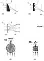
- asymmetric refractive lensessee FIG. 1 ( a )
- asymmetric diffractive lensessee FIG. 1 ( b )
- diffractive gratingssee FIG. 1 ( c )
- Devices embedding asymmetric refractive lensesrely on the phase delay experienced by the rays propagating through a dielectric material 2 with a refractive index n 2 higher than that (n 1 ) of the host medium 1 .
- the transmitted raysfocus in the focal plane FP.
- the optical power of such a componentdepends on the refractive index ratio at the boundaries of the lens, as well as on the curvature of its convex surface. Its effectiveness depends on the size, surface quality, and fabrication tolerance of the lens surfaces. The required fabrication accuracy can be achieved quite easily for large-size lenses, which dimensions are much larger than the wavelength (which is typical for optical applications).
- Devices embedding asymmetric diffractive lensesrely on the diffraction phenomenon.
- such lensesmay take the form of a zoned dielectric plate with variable groove width, which can be optimized to provide a desired optical power and light deviation angle.
- the light deviating functionis implemented by breaking the symmetry of the structure, similarly as in the case of asymmetric refractive lenses.
- Diffractive lenseshave a planar technology that fits well both optical and nano-photonic applications. It is also compatible with established micro- and nano-scale fabrication techniques, such as photolithography. However, diffractive lenses intrinsically suffer from strong chromatic aberration that may not be acceptable for some applications.
- a tilted focused beamcan be generated by a diffraction grating 3 (see FIG. 1 ( c ) ).
- a diffraction grating 3can be implemented in the form of periodic grooves or strips, which period defines the light deviation angles observed for the first and higher diffraction orders.
- Such gratingsare easy to implement, which makes them attractive for both optical and photonic applications. However, like diffractive lenses, they intrinsically suffer from chromatic aberrations. Moreover, the gratings always give rise to multiple beams associated with different diffraction orders, which may not be acceptable for some applications.
- an additional weakness of the devices of FIG. 1is that the spatial resolution of such far-field focusing systems is limited by the Abbe diffraction limit set by ⁇ /2n sin ⁇ , where ⁇ is the vacuum wavelength, n is the host media refractive index, and ⁇ is the half aperture angle of the lens.
- ⁇is the vacuum wavelength
- nis the host media refractive index
- ⁇is the half aperture angle of the lens.
- microspherescan simultaneously provide the subwavelength resolution and a high level of field intensity enhancement (also noted FIE). As shown on FIG. 1( d ) , they allow generating a nanojet beam NB.
- microspheresare associated with certain difficulties related to their (i) precise positioning, (ii) integration with other optical components, and (iii) non-compatibility with the established planar fabrication techniques. These difficulties affect feasibility and increase the fabrication and assembly costs of the nanojet based devices. Potentially, the assembly problem can be solved using nanoscale patterned structures or hollow tubing (see the document U.S. Pat. No. 8,554,031), but these solutions may not be compatible with some applications.
- the SDC lenseswhen illuminated by a plane wave, can also produce condensed beams TB, similar to the nanojet beams observed for microspheres, with subwavelength dimensions, provided the size and shape of cuboids is properly adjusted with respect to the incident wavelength and the refractive index of the cuboid material.
- the best spatial resolution( ⁇ /2, where ⁇ is the wavelength in the host medium) and field intensity enhancement (factor of ⁇ 10) is achieved for SDC with dimensions of about one wavelength in the host medium and the refractive index ratio n 2 /n 1 ⁇ 1.5, where n 1 and n 2 are refractive indexes of the host medium and cuboid material, respectively.
- SDC lensescan be advantageous for some planar fabrication methods (e.g. micromachining or lithography), the fabrication of SDC lenses operating in the optical range can be difficult or even impossible because of the following constraints:
- such near-field focusing componentsenabling the sub-wavelength resolution, do not allow producing the required light deviation function.
- FIGS. 1( d ) and 1( e )where the arrows schematically show formation of nanojet beams when such components are illuminated by a plane wave from below, and where the elongated “jet-like” shape corresponds to the focal region, such components produce nanojet beams, which axis nearly coincides with the incident wave propagation direction.
- references in the specification to “one embodiment”, “an embodiment”, “an example embodiment”,indicate that the embodiment described may include a particular feature, structure, or characteristic, but every embodiment may not necessarily include the particular feature, structure, or characteristic. Moreover, such phrases are not necessarily referring to the same embodiment. Further, when a particular feature, structure, or characteristic is described in connection with an embodiment, it is submitted that it is within the knowledge of one skilled in the art to affect such feature, structure, or characteristic in connection with other embodiments whether or not explicitly described.
- the present disclosureis directed to a device for forming at least one tilted focused beam in a near zone, from an electromagnetic wave incident on said device.
- Such a deviceis remarkable in that it comprises at least one layer of dielectric material comprising at least partially at least one cavity, said at least one cavity being filled in with a medium having a refractive index lower than that of said dielectric material.
- said at least one cavitycomprises at least one base surface, defined with respect to an arrival direction of said electromagnetic wave, and at least one lateral surface.
- Said at least one base surfaceis delineated by a base edge line which comprises at least two opposite base edge line segments comprising at least one concave base edge line segment and at least one convex base edge line segment, which shape and/or orientation and/or associated base angles between said at least one base surface and said at least one lateral surface control an angular position of a projection of said at least one focused beam in a plane orthogonal to said arrival direction of said electromagnetic wave and comprising at least part of said at least one base surface, called an azimuth angle.
- the tilted focused beamis formed thanks to a recombination of nanojet beams originating from different portions of the concave base edge line, and a direction of the tilted focused beam is different from a direction of the incident electromagnetic wave.
- the present disclosureprovides a new type of device for forming desired field intensity distribution in the near zone, with the aid of purely dielectric microstructures. More precisely, such devices are remarkable in that they provide simultaneously focusing and light deviation functions. In other words, they allow focusing electromagnetic waves and generating condensed low-dispersive optical beams (so-called nanojets) in the near zone from a plane electromagnetic wave incident on the device; they also allow controlling the azimuth angle of such nanojets, thanks to an appropriate choice of the parameters of the device's structure, namely the length and curvature of the concave and convex segments of the base edge line, as well as the base angles between the base and lateral surfaces of the cavity.
- the lateral surface of the cavityneed not necessarily be vertical, and may show an angle with respect to the normal to the surface of the dielectric layer.
- base edge lineit is meant here, and throughout the present document, both an actual base edge line, in case the bottom surface forms an angle with the lateral surface of the cavity, and a shadow, or imaginary, base edge line, in case there is a burr or a passing between the bottom surface and the lateral surface of the cavity, with a smooth rounded transition between both.
- the plane in which the azimuth angle is definedis a horizontal plane comprising the base surface of the cavity, in case the electromagnetic wave is incident normal to the base surface, and the base surface forms an angle with the lateral surface of the cavity. More generally, such a plane is orthogonal to the arrival direction of the incident EM wave, and substantially tangent to the base surface, in case the transition between the base surface and the lateral surface of the cavity is not sharp but somehow rounded.
- the dielectric layermay notably be flexible.
- the medium filling the cavitymay simply be air, another gas, vacuum, a liquid or any other material with a refractive index lower than that of the dielectric material.
- a ratio between said refractive index of said medium filling said at least one cavity and said refractive index of said dielectric materialcontributes to controlling an angular position of a projection of said at least one focused beam in a vertical plane, called an elevation angle.
- Such an elevation anglenot only depends on the ratio of refractive indexes, but also on the base angle of the cavity. It may also be influenced by the size/shape of the concave segment of the cavity's base surface edge line.
- such a deviceallows controlling both the azimuth and elevation angles of the focused beam, thus achieving a complete control of the electromagnetic wave deviation, which makes it very attractive for many nano-photonic applications.
- said at least one cavityis targeted to be cylindrical or cone-shaped (i.e. said at least one cavity is approximately cylindrical or cone-shaped) and said base edge line has a shape of a crescent moon, comprising a concave base edge line segment and a convex base edge line segment.
- cylindrical cavityit is meant here, and throughout this document, a cavity which shape is a generalized cylinder, i.e. a surface created by projecting a closed two-dimensional curve along an axis intersecting the plane of the curve.
- a cylinderis not limited to a right circular cylinder but covers any type of cylinder, notably, but not exclusively, a cuboid or a prism for example.
- the cavitymay also have the form of a cone. Its main axis may be orthogonal to the surface of the bottom of the cavity, or be tilted. Due to the fabrication tolerance, the cavities may also have imperfect shapes, and it must be understood, for example, that cavities targeted to be shaped as cylinders, may become cone-shaped cavities during the manufacturing process.
- the cavitymay have the shape of a hollow cylinder with a crescent moon cross section.
- the base edge line of such a cavitycomprises two line segments adjacent to the convex and concave surfaces of the cylindrical cavity.
- the convex segment of the base edge lineproduces a wide diverging beam of a conical type, while the concave segment of the base edge line acts like a focusing element producing a focused nanojet beam that is formed thanks to the recombination of the nanojet beams originating from different portions of the concave segment of the base edge line.
- Such a cavity with a crescent moon cross sectionis easy to manufacture through established microfabrication techniques (like molding (e.g. nanoimprinting) or photolithography) by superimposing (i.e. subtracting) two circular cylinders.
- microfabrication techniqueslike molding (e.g. nanoimprinting) or photolithography
- said at least one cavitybelongs to at least one set of at least two cavities.
- Cavitiesmay be arranged into arrays of cavities, or non-regular arrangements forming a peculiar pattern, in order to generate specific focused beams in the near zone, or an array of beams, which deviation may be controlled.
- the arrays of cavitiesmay be planar (with all base faces of all cavities lying in the same plane) or not, and can be made of identical cavities or not.
- the microstructuremay comprise any number of cavities arranged in one plane (i.e. at a surface of a single plate) and placed far enough from each other to avoid electromagnetic coupling (i.e. at least a few wavelengths in the host medium). Thanks to this, each microcavity produces an independent nanojet beam, which parameters (Full Width at Half Maximum (FWHM) and deviation angle) depend on the parameters of the corresponding microcavity.
- FWHMFull Width at Half Maximum
- said cavities in said setare at least partly merged to form at least one arrangement of cavities.
- cavitiesmay be combined to form a periodic S-type curved groove, or a gear-type cavity formed by merging several cavities with a crescent moon shape.
- a gearmay have different radii of concave segments or may only have two or three identical or non-identical concave segments.
- a devicemay also comprise several gear-type cavities, whether identical or not, rotated in horizontal plane. It may also comprise an arrangement of S-type grooves, whether of identical or non-identical shape, i.e. with a varying radius of concave segments.
- a devicemay comprise a first S-type curved groove with all identical segments of radius R 1 , a second S-type curved groove of all identical segments of radius R 2 , a third S-type curved groove of all identical segments of radius R 3 , etc.
- itmay also comprise one or several S-type curved grooves, with radius of the concave segments varying along the groove.
- the shape of the cavitycan be generalized towards a more complex structure comprising a set of crescent moon elements combined together.
- a structurecan be designed to produce a more complex optical function, as well as for gaining additional degrees of freedom for near-field patterning and/or for simplifying the fabrication/assembly process.
- such a devicefurther comprises at least one layer forming a substrate abutting said at least one layer of dielectric material.
- Such a substratemay contribute to the mechanical rigidity of the device.
- such a devicefurther comprises at least one layer forming a superstrate, said at least one layer of dielectric material being located between said substrate and said superstrate.
- the devicemay take the form of a planar optically-transparent element, comprising two glass or plastic plates (namely the substrate and the superstrate), between which a dielectric material with void or filled hollow microcavities is embedded.
- the superstratemay of course be non-planar, and follow the shape of the substrate for example.
- the pattern of the field intensity distribution generated by the device when illuminated by a plane wave incident normal to the basesolely depends on the cavity base angle (or step angle), on the cavity cross-section shape, and on the index ratio between the dielectric material and the medium filling the cavity (or covering the lower part of the surface with respect to the step).
- the radiation of the beamswill change for incline incidence of the plane wave, with a shape of the beam well preserved for the incident angles of about +1/ ⁇ 30°, depending on the size, base angle and curvature of the cavity base edge line.
- said substrate and said superstrateare made of the same dielectric material as said at least one layer of dielectric material.
- said dielectric material forming said at least one layer of dielectric materialbelongs to the group comprising:
- airis not considered as a candidate dielectric material for the device according to the present disclosure.
- Such a devicecan hence be fabricated using standard dielectric materials, which are easy to find and inexpensive.
- a material of said superstratebelongs to the group comprising:
- a material of said substratebelongs to the group comprising:
- the medium having a refractive index lower than that of said dielectric materialbelongs to the group comprising:
- FIGS. 1 ( a ), ( b ), ( c ), ( d ) and ( e )relate to prior art techniques and are schematic drawings illustrating operational principles of refractive lenses, diffractive lenses, diffractive gratings, nanojet microlenses and terajet solid cuboid lenses;
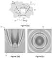
- FIG. 2( a )illustrates the topology of a hollow cylindrical cavity formed in a layer of dielectric material and producing a conical-type nanojet beam when illuminated by a plane wave from below, while FIG. 2( b ) illustrates the normalized near-field power density distribution in the vertical xz-plane and FIG. 2( c ) illustrates the normalized power density distribution in the horizontal xy-plane;
- FIGS. 3A and 3Brespectively show a 3D view and a top view of a device for forming a tilted focused beam in the near-zone according to an embodiment of the present disclosure
- FIGS. 4( a ), ( b ) and ( c )present normalized near-field power density distribution in horizontal and vertical planes for the nanojet microlens of FIG. 3 illuminated by a linearly polarized plane wave from below, at different wavelengths;
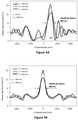
- FIG. 5presents the nanojet beam profile, as generated by the device of FIG. 3 , along the x-axis ( FIG. 5A ) and along the y-axis ( FIG. 5B );
- FIG. 6presents the peak power density in the nanojet beams produced by the convex and concave segments of the nanojet device with a crescent moon shape of FIG. 3 ;
- FIG. 7provides an alternate embodiment to FIG. 3 , in which the device presents a variable base angle
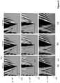
- FIGS. 8( a ) to 8( c )show the normalized field intensity patterns in xz-plane of the nanojet beam created by the device of FIG. 7 , for different values of the base angle and different wavelengths of an incident TE-polarized plane wave;
- FIGS. 9( a ) to 9( c )show the normalized field intensity patterns in xz-plane of the nanojet beam created by the device of FIG. 7 , for different values of the base angle and different wavelengths of an incident TM-polarized plane wave;
- FIGS. 11( a ) and 11( b )illustrate the nanojet beam radiation angle with respect to the step base angle of the device of FIG. 7 for three different wavelengths, respectively for a TE polarization ( FIG. 11( a ) ), and for a TM polarization ( FIG. 11( b ) );
- FIGS. 12( a ) to 12( d )illustrate an alternate embodiment to the device of FIG. 3 , according to which several devices with a crescent-moon shape are assembled in order to form a periodic S-type curved groove in a host dielectric medium;
- FIGS. 13( a ) to 13( c )illustrate a further alternate embodiment to the device of FIG. 3 , according to which several devices with a crescent moon shape are assembled in order to form a cavity with a gear-type cross section;
- FIG. 14illustrates an example of a device that can be used to control performance of a device according to one embodiment of the disclosure.
- the general principle of the present disclosurerelies on the design of a new dielectric microstructure, which may be used for generating condensed low-dispersive optical beams in the near zone, also called nanojets, while simultaneously controlling their deviation. Its use is not limited to optical wavelengths. Presence of hollow cavities in the dielectric microstructure gives rise to a diffraction phenomenon, which is in turn coupled to refraction and interference phenomena, and allows generating condensed beam(s) of radiation in the near zone, with a controlled deviation, when the dielectric microstructure is illuminated by a plane wave, depending on the shape and dimensions of the structure.
- the beam-forming and deviation function of such nanojet devicesmay be controlled by setting the cavity's base edge line length and curvature, as well as its base angle.
- Such a general principleallows designing new focusing and beam-forming components, which can replace the conventional focusing devices in dense optic and photonic systems, like integrated optical sensors used in photo/video cameras that are essential components in the field of mobile technology (e.g. smartphones, tablets, AR and VR glasses).
- the present disclosurefinds applications in many fields of technology, including, but not limited to:
- Inventors of the present disclosurehave reached the conclusion that diffraction of a plane electromagnetic wave on the base surface of a dielectric material in the close vicinity of an abrupt change of level of this surface, also called a step, can result in the formation of condensed optical beams (so-called nanojets), when the surface on which diffraction occurs is in contact with a medium (material or gas) having a lower refractive index than that of the dielectric material.
- the number of beams and shape of each individual beamcan be controlled by the variation of the step size and shape of the step edge line adjacent to the lateral and lower surfaces of the step.
- the nanojet beamsare low-dispersive (they show no or small wavelength dependence).
- a same nanojet focusing component according to the present disclosurecan produce multiple independent beams (having identical or non-identical shape) associated with different segments of the step edge line, which is not possible with Fresnel diffractive lenses.
- FIGS. 2( a ) to 2( c )illustrate this general principle, according to which diffraction of a plane wave by a hollow cylindrical cavity as shown on FIG. 2( a ) , created in a dielectric host medium, results in the formation of a focused beam (i.e. nanojet), whose cross-section shape in the plane orthogonal to the incident wave propagation direction reproduces the shape of the cavity base edge line.
- a focused beami.e. nanojet
- the cavity 22has a circular cross-section.
- the nanojet beam 23is created as a result of the interference between a refracted wave, which is radiated outside the cavity 22 and the plane wave incident from below.
- the angle of radiation of the nanojet beam ( ⁇ B )is defined by a vector sum of these two waves.
- the refraction angle of the wave radiated outward the cavityis close to the critical angle for the wave incident on the same boundary from outside: ⁇ 1 ⁇ TIR , since the main contribution to the formation of the planar wave front of the refracted wave outside the cavity comes from Huygens sources located close to the lateral edge of the cavity 22 .
- the peak field intensity in the nanojet beamdepends on the dimensions of the cavity, base angle, and curvature of its base edge line.
- a new type of nanojet microlensis hence introduced, whose shape resembles young moon, and which provides control over the azimuth and elevation angles of the focused nanojet beam.
- FIG. 3Aprovides a 3D view of such a nanojet microlens with schematic illustration of the individual nanojet beams associated with different portions of the base edge line.
- the base surface 321 of the cavity 32is delineated by a base edge line 322 , represented by a piecewise curve which comprises at least one convex part and at least one concave part.
- the base edge line 322comprises two line segments adjacent to the convex and concave surfaces of the cylindrical cavity 32 .
- the convex segment of the base edge line 322(formed by base edge line segments 322 1 , 322 2 , 322 3 , . . . ) produces a wide diverging beam of a conical type similar to the one shown in FIGS. 2( a ) to 2( c ) , and comprising the nanojet beams 33 2 , 33 2 , 33 3 .
- the concave segment 322 4 of the base edge line 322acts like a focusing element producing a focused NJ beam 33 4 , which is formed thanks to the recombination of the NJ beams originating from different portions of the concave segment 322 4 of the base edge line 322 .
- the radiation angle of the nanojet beam 33 4i.e. light deviation angle in the vertical (elevation) plane, is mainly defined by the index ratio at the boundary of the cavity 32 . It also depends on the base angle of the cavity and, possibly, on the size/shape of the concave segment of its base surface edge line.
- Orientation of the beam in the horizontal (azimuthal) planecan be varied by rotating the moon-like cavity around its vertical axis (i.e. z-axis in FIGS. 3A-3B ).
- orientation of the nanojet beam in the horizontal planecan be characterized by an azimuth angle counted with respect to x-axis.
- the lens with a crescent moon shapeis created by superimposing (i.e. subtracting) two circular cylinders 34 1 , 34 2 having the same height but different radii R 1 and R 2 .
- the distance between both cylinders 34 1 , 34 2is a variable parameter W.
- the right images in xz-plane at y0.
- the power density distribution in the near zone of a hollow cavity with a crescent moon shapeagrees well with the theoretical model presented in FIG. 3 .
- a tilted focused beam 33 4can be identified on the concave side of the cavity 32 .
- the beam full width at half maximum (FWHM)is about 480 nm in both planes.
- Two reference solutionsare also shown, which correspond to the power density of a plane wave propagating in the same host medium (line 63 ) and to a nanojet beam produced by a straight edge of an infinite groove (line 64 ).
- FIGS. 7 to 11illustrate the existing relation between the cavity base angle of the nanojet device and the nanojet beam radiation angle.
- FIG. 7first gives some notations, which will be used thereafter.
- a cavity 32is formed in a dielectric host medium 31 .
- Cavity 32comprises a base surface, or lower part, 321 and a lateral part 323 , which forms a base angle 70 ⁇ with the base surface 321 .
- the cavity 32forms a step, i.e. an abrupt change of level in the dielectric host medium 31 . It is considered in FIG. 7 that the step is infinite along y-direction, as compared to the wavelength of the incident electromagnetic wave 20 .
- the cavity edge linesextend to infinity in the negative x- and positive z-directions, as compared to the wavelength.
- a nanojet beam 33 4is produced by this step with base angle 70 ⁇ . It shows a radiation angle 71 , noted as ⁇ B , measured from the z axis.
- FIGS. 9( a ) to 9( c )show the normalized field intensity patterns in xz-plane of the nanojet beam created by the device of FIG. 7 , for different values of the base angle 70 ⁇ and different wavelength of the incident EM wave 20 .
- the value of the base angle 70 ⁇thus influences the radiation angle of the nanojet beam created by the step of the device of FIG. 7 .
- the x axiscorresponds to the x coordinates expressed in nm.
- FIGS. 11( a ) and 11( b )illustrate the nanojet beam radiation angle ⁇ expressed in degrees with respect to the step base angle 70 ⁇ , also expressed in degrees, for three different wavelengths, namely 450 nm, 550 nm and 650 nm.
- FIG. 11( a )corresponds to a TE polarization
- FIG. 11( b )corresponds to a TM polarization of the incident EM wave 20 .
- the nanojet beam radiation angleis defined as follows:
- the nanojet beam radiation for the right anglecan be approximately defined by equation (1), as mentioned previously.
- the mismatch between Eq. (4) and the data extracted from the full-wave EM simulationsdoes not exceed 3° for all values of the base angle 70 ⁇ .
- the nanojet microlenses with crescent moon shape according to the present disclosureare near-zone focusing devices, which are used in association with other optical elements, such as focusing, beam-forming, light guiding or light capturing components. To increase their overall efficiency, it may be advantageous to use arrays of such nanojet elements, which may comprise from a few to several hundreds of cavities. These arrangements of moon-like nanojet microlenses can be created either on surface of the component tor inside the volume.
- a devicemay comprise any number of cavities arranged in one plane (i.e. at a surface of a single plate) and placed far enough from each other to avoid electromagnetic coupling (i.e. at least a few wavelength in the host medium). Thanks to this, each microcavity will produce an independent nanojet beam, which parameters (FWHM and deviation angle) will depend on the parameters of the corresponding microcavity.
- Multi-layers structures with two or more arrangements of nanojet microcavities arranged in different horizontal planesare also possible.
- the nanojet cavitiesmay be preferable to arrange the nanojet cavities so as to form an array, either with a regular or an irregular layout.
- Such an arraymay comprise any number of identical or non-identical cavities (in terms of size, shape and orientation).
- itcan comprise identical nanojet cavities with a crescent moon shape with different orientation or an array of groups of nanojet cavities arranged in accordance to a determined pattern in order to produce a more complex optical function.
- Thiscan be a certain near-field pattern or a larger-scale focused beam, produced as a result of recombination of independent nanojet beams associated with different microcavities, that extends beyond the near-zone of a single nanojet microlens.
- the shape of the nanojet cavitycan also be generalized towards a more complex structure comprising a set of moon-like elements combined together.
- a structurecan be designed to produce a complex optical function, as discussed above, or for gaining additional degrees of freedom for near-field patterning and/or for simplifying the fabrication/assembly process.
- FIGS. 12 and 13show possible examples of such arrangements of moon-like nanojet microlenses.
- FIGS. 12( a ) to 12( d )illustrate an alternate embodiment to the device of FIG. 3 , according to which several devices with a crescent-moon shape are assembled in order to form a periodic S-type curved groove in a host dielectric medium.
- FIG. 12( a )presents a perspective view of a dielectric plate 121 , within which a generalized crescent moon like focusing element having a form of a periodic S-type curved groove 122 is created. More precisely, FIG. 12( a ) shows the topology of a unit cell of such a periodic groove, placed in free space 123 , and engraved at the surface of a dielectric substrate 121 .
- FIG. 12( b )illustrates the near-field intensity pattern in xy-plane at a close distance above the plate surface 121 .
- FIG. 12( c )provides a 3D view of the field intensity pattern of the unit cell of FIG. 12( a ) .
- FIG. 12( d )illustrates the field intensity pattern in a 2D xz-plane crossing a nanojet beam.
- the periodic S-type curved groove 122is formed by a cavity that comprises at least one base surface, defined with respect to an arrival direction of said electromagnetic wave, and at least one lateral surface, and said at least one base surface is delineated by a base edge line which has portions, each portion having a U-shape or C-shape or a crescent moon-shape (depending of the viewing orientation), that comprises a concave base edge line segment and a convex base edge line segment.
- FIGS. 13( a ) to 13( c )illustrate a further alternate embodiment, according to which several devices with a crescent moon shape are assembled in order to form a cavity with a gear-type cross section with four identical concave segments, created in a double-layer dielectric plate.
- FIG. 13( a )illustrates the topology of such a gear-type cavity 132 , created in a dielectric plate 131 .
- FIG. 13( b )shows the near-field intensity pattern in xy-plane at a close distance above the plate 131 surface;
- FIG. 13( c )shows the field intensity pattern in xz-plane passing through the center of the cavity 132 and its concave segments.
- FIGS. 13( a )illustrates the topology of such a gear-type cavity 132 , created in a dielectric plate 131 .
- FIG. 13( b )shows the near-field intensity pattern in xy-plane at a close distance above the plate 131 surface;
- FIG. 13( c )shows the field intensity pattern in xz-plane passing through the center of the cavity 132 and its concave segments.
- the host medium refractive index n 11.5
- the gear-type cavity 132comprises at least one base surface, defined with respect to an arrival direction of said electromagnetic wave, and at least one lateral surface, and said at least one base surface is delineated by a base edge line which has at least four portions that have a U-shape or C-shape or a crescent moon-shape (depending of the viewing orientation), that comprises a concave base edge line segment and a convex base edge line segment.
- such devices embedding one or several cavities with a crescent moon shape in a dielectric microstructurecan be fabricated using any established microfabrication technique, like molding (e.g. nanoimprinting) or photolithography.
- such a componentcan take the form of a plate made of an optically transparent material (e.g. glass, plastic, polymer) with a microstructure formed on one of its surfaces.
- the platecan be planar or curved, flexible (bendable).
- the platecan be made of a single material or may comprise several layers. The former option is more suitable for resist-free molding fabrication methods, while the latter is more relevant to photolithography techniques.
- the plate with engraved microstructurecan be attached to another component, e.g. another dielectric plate or a plano-convex lens.
- the nanojet cavitiesmay be formed on the external surface of the compound component, or at the interface between the two attached components.
- the proposed componentin all its embodiments, can be, for instance, fabricated in the form of a thin film with perforated apertures attached to a glass plate or directly to a surface of another optical component, e.g. a plano-convex lens. It can also be covered with another layer of an optically-transparent media (e.g. another glass plate).
- the filmcan be made of an optically transparent material, like PMMA (Acrylic), that is to be deposited directly on the surface of the supporting component (e.g. glass plate or lens). For instance, this can be done by spin-coating that enables deposition of thin nanofilms with the desired thickness (order of a few hundred nanometers).
- the apertures(that will serve as hollow cuboids) can then be created, for instance, using the optical or e-beam lithography technology.
- the periodic structurescan be, potentially, fabricated using the maskless interference lithography that is faster and cheaper than standard optical lithography.
- the cavities with a crescent moon shapecan be fabricated using nanoimprinting or replica molding methods in an optically transparent material, e.g. soft organic polymer such as PDMS, and then attached to a surface of a glass plate acting as a support.
- an optically transparent materiale.g. soft organic polymer such as PDMS
- FIG. 14presents an example of a device that can be used to control the performance of a device according to one embodiment of the disclosure.
- Such a device referenced 1400comprises a computing unit (for example a CPU, for “Central Processing Unit”), referenced 1401 , and one or more memory units (for example a RAM (for “Random Access Memory”) block in which intermediate results can be stored temporarily during the execution of instructions a computer program, or a ROM block in which, among other things, computer programs are stored, or an EEPROM (“Electrically-Erasable Programmable Read-Only Memory”) block, or a flash block) referenced 1402 .
- Computer programsare made of instructions that can be executed by the computing unit.
- Such a device 1400can also comprise a dedicated unit, referenced 1403 , constituting an input-output interface to allow the device 1400 to communicate with other devices.
- this dedicated unit 1403can be connected with an antenna (in order to perform communication without contacts), with light source/receiving unit (such as for example a photodiode, optical fiber, detector, e.g. photodiode, etc.) or with serial ports (to carry communications “contact”).
- light source/receiving unitsuch as for example a photodiode, optical fiber, detector, e.g. photodiode, etc.
- serial portsto carry communications “contact”.
- control of the performance of a devicecan be implemented in hardware in a programmable FPGA (“Field Programmable Gate Array”) component or ASIC (“Application-Specific Integrated Circuit”) component.
- a programmable FPGAField Programmable Gate Array
- ASICApplication-Specific Integrated Circuit
Landscapes
- Physics & Mathematics (AREA)
- General Physics & Mathematics (AREA)
- Optics & Photonics (AREA)
- Diffracting Gratings Or Hologram Optical Elements (AREA)
- Aerials With Secondary Devices (AREA)
Abstract
Description
- Strict requirements imposed on the cuboid size and shape;
- Absence of materials with the desired refractive indexes (in the optical range, the refractive index of common optical glass and plastics, which can be used as a host medium, varies from n1≈1.3 up to 2.0, whereas, according to the article “Terajets produced by dielectric cuboids”, the desired value of the cuboid lens refractive index should be n2˜2.25 (follows from the suggested ratio n1/n2=1.5 and the refractive index value of a standard glass n1≈1.5) that is out of range for standard optical materials;
- No solution provided for setting the position of such lenses in space. This is a critical point because of the miniature size of the cuboids.
- glass;
- plastic;
- a polymer material, such as PMMA (Poly(methyl methacrylate)) or PDMS (Polydimethylsiloxane);
- an organic or inorganic optically transparent electrically conducting material (such as indium tin oxide (ITO) or doped zinc oxide (ZnO) for example);
- ceramics.
- glass;
- plastic;
- a polymer material;
- an organic or inorganic optically transparent electrically conducting material (such as indium tin oxide (ITO) or doped zinc oxide (ZnO) for example);
- a semiconductor material;
- a liquid;
- a gas;
- a gel.
- glass;
- plastic;
- a polymer material;
- an organic or inorganic optically transparent electrically conducting material (such as indium tin oxide (ITO) or doped zinc oxide (ZnO) for example);
- a semiconductor material;
- a liquid;
- a gas;
- a gel.
- glass;
- plastic;
- a liquid;
- a gas;
- a gel.
- eyewear electronics, including AR and VR glasses;
- optical sensors for photo/video/light field cameras;
- light communication systems, including quantum computers;
- bio/chemical sensors, including lab-on-chip sensors;
- microscopy, spectroscopy and metrology systems;
- integrated lens antennas for applications in the millimeter/sub-millimeter/infrared (IR) wavelength ranges.
where xiis x-coordinate of a point corresponding to the peak intensity value in a cut plane zi, i=1,2,3, as shown in
θ≈θB+(α−90°)/3 (4)
where θBis the NJ radiation angle observed for the base angle α=90°. Moreover, the nanojet beam radiation for the right angle can be approximately defined by equation (1), as mentioned previously.
Claims (18)
Applications Claiming Priority (4)
| Application Number | Priority Date | Filing Date | Title |
|---|---|---|---|
| EP16306387.8AEP3312660A1 (en) | 2016-10-21 | 2016-10-21 | Device for forming at least one tilted focused beam in the near zone, from incident electromagnetic waves |
| EP16306387.8 | 2016-10-21 | ||
| EP16306387 | 2016-10-21 | ||
| PCT/EP2017/076877WO2018073426A1 (en) | 2016-10-21 | 2017-10-20 | Device for forming at least one tilted focused beam in the near zone, from incident electromagnetic waves |
Publications (2)
| Publication Number | Publication Date |
|---|---|
| US20200348526A1 US20200348526A1 (en) | 2020-11-05 |
| US11275252B2true US11275252B2 (en) | 2022-03-15 |
Family
ID=57944243
Family Applications (1)
| Application Number | Title | Priority Date | Filing Date |
|---|---|---|---|
| US16/342,036Active2037-10-22US11275252B2 (en) | 2016-10-21 | 2017-10-20 | Device for forming at least one tilted focused beam in the near zone, from incident electromagnetic waves |
Country Status (4)
| Country | Link |
|---|---|
| US (1) | US11275252B2 (en) |
| EP (2) | EP3312660A1 (en) |
| CN (1) | CN110168432B (en) |
| WO (1) | WO2018073426A1 (en) |
Cited By (14)
| Publication number | Priority date | Publication date | Assignee | Title |
|---|---|---|---|---|
| US20220059250A1 (en)* | 2018-12-18 | 2022-02-24 | Interdigital Ce Patent Holdings, Sas | Optical manipulation apparatus |
| US11443491B2 (en)* | 2019-06-28 | 2022-09-13 | Snap Inc. | 3D object camera customization system |
| US11501499B2 (en) | 2018-12-20 | 2022-11-15 | Snap Inc. | Virtual surface modification |
| US11620791B2 (en) | 2018-11-27 | 2023-04-04 | Snap Inc. | Rendering 3D captions within real-world environments |
| US11704878B2 (en) | 2017-01-09 | 2023-07-18 | Snap Inc. | Surface aware lens |
| US11715268B2 (en) | 2018-08-30 | 2023-08-01 | Snap Inc. | Video clip object tracking |
| US11908093B2 (en) | 2019-12-19 | 2024-02-20 | Snap Inc. | 3D captions with semantic graphical elements |
| US11972508B2 (en) | 2018-07-02 | 2024-04-30 | Interdigital Ce Patent Holdings, Sas | Image sensor comprising a color splitter with two different refractive indexes, and different height |
| US12175613B2 (en) | 2019-12-19 | 2024-12-24 | Snap Inc. | 3D captions with face tracking |
| US12174512B2 (en) | 2018-12-18 | 2024-12-24 | Interdigital Ce Patent Holdings | Device for forming an outgoing electromagnetic wave from an incident electromagnetic wave |
| US12210155B2 (en) | 2018-06-29 | 2025-01-28 | Interdigital Ce Patent Holdings | Optical device comprising a multi-layers waveguides |
| US12228756B2 (en) | 2018-12-21 | 2025-02-18 | Interdigital Ce Patent Holdings, Sas | Optical device |
| US12361652B2 (en) | 2016-10-24 | 2025-07-15 | Snap Inc. | Augmented reality object manipulation |
| US12443325B2 (en) | 2023-05-31 | 2025-10-14 | Snap Inc. | Three-dimensional interaction system |
Families Citing this family (14)
| Publication number | Priority date | Publication date | Assignee | Title |
|---|---|---|---|---|
| EP3223063A1 (en) | 2016-03-24 | 2017-09-27 | Thomson Licensing | Device for forming a field intensity pattern in the near zone, from incident electromagnetic waves |
| EP3312660A1 (en) | 2016-10-21 | 2018-04-25 | Thomson Licensing | Device for forming at least one tilted focused beam in the near zone, from incident electromagnetic waves |
| EP3312646A1 (en) | 2016-10-21 | 2018-04-25 | Thomson Licensing | Device and method for shielding at least one sub-wavelength-scale object from an incident electromagnetic wave |
| EP3385219B1 (en) | 2017-04-07 | 2021-07-14 | InterDigital CE Patent Holdings | Method for manufacturing a device for forming at least one focused beam in a near zone |
| EP3451027A1 (en) | 2017-09-01 | 2019-03-06 | Thomson Licensing | Optical device capable of providing at least two different optical functions |
| EP3540479A1 (en) | 2018-03-13 | 2019-09-18 | Thomson Licensing | Diffraction grating comprising double-materials structures |
| EP3540499A1 (en) | 2018-03-13 | 2019-09-18 | Thomson Licensing | Image sensor comprising a color splitter with two different refractive indexes |
| EP3629076A1 (en) | 2018-09-28 | 2020-04-01 | Thomson Licensing | Device for radiating at least one outgoing electromagnetic wave when illuminated by an incoming electromagnetic wave |
| EP3633437A1 (en)* | 2018-10-01 | 2020-04-08 | InterDigital CE Patent Holdings | Device for near-field focusing and beam forming |
| EP3633438A1 (en)* | 2018-10-01 | 2020-04-08 | InterDigital CE Patent Holdings | Inhomogeneous microlens device for near-field focusing, beam forming, and high-efficiency far-field device implementation |
| EP3632564A1 (en) | 2018-10-01 | 2020-04-08 | Thomson Licensing | System for optical detection and imaging of nanoscale objects |
| EP3671321A1 (en) | 2018-12-18 | 2020-06-24 | Thomson Licensing | Device for forming at least one tilted focused beam in the near-field zone, from incident electromagnetic waves, and image sensor including such a device |
| CN110829035B (en)* | 2019-11-19 | 2021-03-16 | 大连海事大学 | A Circularly Polarized Patch Antenna with Wide Half-Power Beam |
| CN113181556B (en)* | 2021-04-30 | 2022-09-23 | 西北核技术研究所 | An Irradiation Cavity Based on Dielectric Substrate Structure for Enhanced Internal Field Strength of Large-scale Effectors |
Citations (84)
| Publication number | Priority date | Publication date | Assignee | Title |
|---|---|---|---|---|
| US3718383A (en) | 1971-04-19 | 1973-02-27 | Eastman Kodak Co | Plastic optical element having refractive index gradient |
| US3873408A (en) | 1969-10-06 | 1975-03-25 | Bausch & Lomb | Method of producing a refractive index gradient in glass |
| US3904268A (en) | 1974-11-15 | 1975-09-09 | Corning Glass Works | Optical waveguide having optimal index gradient |
| US4952037A (en) | 1985-03-05 | 1990-08-28 | Nippon Sheet Glass Co., Ltd. | Plate microlens and method for manufacturing the same |
| US6236513B1 (en) | 1999-06-30 | 2001-05-22 | Quantum Corporation | Integrated objective/solid immersion lens for near field recording |
| WO2001057559A1 (en) | 2000-02-02 | 2001-08-09 | Trivium Technologies, Inc. | Multiflecting light directing film |
| US20030036674A1 (en) | 2001-07-26 | 2003-02-20 | Bouton Chad Edward | Electromagnetic sensors for biological tissue applications and methods for their use |
| WO2003025635A1 (en) | 2001-09-19 | 2003-03-27 | Technion Research & Development Foundation Ltd. | Space-variant subwavelength dielectric grating and applications thereof |
| US6569575B1 (en) | 1997-09-19 | 2003-05-27 | International Business Machines Corporation | Optical lithography beyond conventional resolution limits |
| US6594430B1 (en) | 2000-05-11 | 2003-07-15 | Carnegie Mellon University | Solid immersion lenses for focusing collimated light in the near-field region |
| EP1398656A1 (en) | 2002-09-12 | 2004-03-17 | Olimatech Ltd. | Surface-plasmon-generated light source and its use |
| US6753131B1 (en) | 1996-07-22 | 2004-06-22 | President And Fellows Of Harvard College | Transparent elastomeric, contact-mode photolithography mask, sensor, and wavefront engineering element |
| US20040165269A1 (en) | 2002-09-13 | 2004-08-26 | Erez Hasman | Space-variant subwavelength dielectric grating and applications thereof |
| US6804189B2 (en) | 2000-04-07 | 2004-10-12 | Tosoh Corporation | Near field optical recording medium |
| JP2005141075A (en) | 2003-11-07 | 2005-06-02 | Dainippon Printing Co Ltd | Diffraction grating phase mask |
| US7057151B2 (en) | 2001-08-31 | 2006-06-06 | Universite Louis Pasteur | Optical transmission apparatus with directionality and divergence control |
| CN1823456A (en) | 2003-06-10 | 2006-08-23 | 福托纳米公司 | Method and apparatus for suppression of spatial-hole burning in second or higher order dfb lasers |
| CN1853131A (en) | 2003-09-18 | 2006-10-25 | 日本电气株式会社 | Optical element |
| CN101088040A (en) | 2004-12-22 | 2007-12-12 | 皇家飞利浦电子股份有限公司 | Apparatus and method for enhanced optical transmission through a small aperture, using radially polarized radiation |
| US20080024792A1 (en) | 2006-07-25 | 2008-01-31 | John Pendry | Electromagnetic Cloaking Method |
| US20080089367A1 (en) | 2006-10-03 | 2008-04-17 | Kartik Srinivasan | Fiber-Coupled Solid State Microcavity Light Emitters |
| WO2008069454A1 (en) | 2006-12-05 | 2008-06-12 | Electronics And Telecommunications Research Institute | Guided mode resonance filter including high refractive index organic material and optical biosensor including the guided mode resonance filter |
| US7394535B1 (en) | 2007-03-20 | 2008-07-01 | Tokyo Electron Limited | Optical metrology using a photonic nanojet |
| WO2008080117A2 (en) | 2006-12-21 | 2008-07-03 | Annulex Inc. | Particle shutter device and associated displays |
| US20080231863A1 (en) | 2007-03-20 | 2008-09-25 | Tokyo Electron Limited | Automated process control using optical metrology with a photonic nanojet |
| US20090068597A1 (en) | 2005-01-14 | 2009-03-12 | Naomasa Shiraishi | Exposure method and apparatus, and electronic device manufacturing method |
| CN101419337A (en) | 2008-11-28 | 2009-04-29 | 中国科学技术大学 | Superresolved phase modulating sheet for flare three-dimensional compression and its processing method |
| US7541115B1 (en) | 2004-11-15 | 2009-06-02 | Kla-Tencor Technologies Corporation | Use of calcium fluoride substrate for lithography masks |
| US7612883B2 (en) | 2007-05-17 | 2009-11-03 | General Electric Company | Dynamic plasmonics-enabled signal enhancement, a device comprising the same, and a method using the same |
| US20100006784A1 (en) | 2008-07-09 | 2010-01-14 | Michael Mack | Method and system for a light source assembly supporting direct coupling to an integrated circuit |
| CN101819326A (en) | 2010-04-15 | 2010-09-01 | 北京交通大学 | Photonic crystal optical fiber coupler for forming hollow light beam and preparation method thereof |
| WO2010114834A1 (en) | 2009-03-30 | 2010-10-07 | The Trustees Of The University Of Pennsylvania | Cloaked sensor |
| WO2010114857A1 (en) | 2009-03-30 | 2010-10-07 | Time Warner Cable Inc. | Recommendation engine apparatus and methods |
| US20100265590A1 (en) | 2009-04-17 | 2010-10-21 | Searete Llc, A Limited Liability Corporation Of The State Of Delaware | Evanescent electromagnetic wave conversion apparatus I |
| US20100320213A1 (en) | 2007-01-12 | 2010-12-23 | Millercoors, Llc | Double walled beverage container and method of making same |
| US20100320513A1 (en) | 2008-01-31 | 2010-12-23 | Nxp B.V. | Semiconductor device and a method of manufacturing the same |
| JP2011014857A (en) | 2009-06-05 | 2011-01-20 | Nec Corp | Optical element, photon generator using the same, light generator, optical recorder, and photodetector |
| US20110063717A1 (en) | 2008-05-20 | 2011-03-17 | Universite De Technologie De Troyes | High-efficiency device for focusing light to subwavelength dimensions |
| US8003965B2 (en) | 2007-05-18 | 2011-08-23 | The Regents Of The University Of Michigan | Apparatus for sub-wavelength near-field focusing of electromagnetic waves |
| US8052908B2 (en) | 2007-05-02 | 2011-11-08 | University Of Maryland | Photolithographic mask exhibiting enhanced light transmission due to utilizing sub-wavelength aperture arrays for imaging patterns in nano-lithography |
| KR20120111288A (en) | 2011-03-31 | 2012-10-10 | 국민대학교산학협력단 | Methode of forming fine patterns using nano imprint mold and photo mask |
| US20120326309A1 (en) | 2011-06-23 | 2012-12-27 | International Business Machines Corporation | Optimized annular copper tsv |
| CN102916343A (en) | 2011-08-05 | 2013-02-06 | 苏州大学 | Production device and production method for quantum dot material |
| US8448247B2 (en) | 2002-03-29 | 2013-05-21 | Global Dataguard Inc. | Adaptive behavioral intrusion detection systems and methods |
| US8488247B2 (en) | 2008-10-06 | 2013-07-16 | Purdue Research Foundation | System, method and apparatus for modifying the visibility properties of an object |
| US8508830B1 (en) | 2011-05-13 | 2013-08-13 | Google Inc. | Quantum dot near-to-eye display |
| US8554031B2 (en) | 2009-06-17 | 2013-10-08 | University Of North Carolina At Charlotte | Focusing multimodal optical microprobe devices |
| US8552416B2 (en) | 2010-05-25 | 2013-10-08 | Lg Display Co., Ltd. | Quantum dot light emitting diode device and display device therewith |
| CN103353675A (en) | 2013-07-02 | 2013-10-16 | 浙江大学 | Frequency-shift super-resolution microscopic imaging method and device based on microstructure |
| US20130308127A1 (en) | 2012-05-16 | 2013-11-21 | Indian Institute Of Technology Madras | Enhancement of raman scattering |
| US20130335677A1 (en) | 2012-06-15 | 2013-12-19 | Apple Inc. | Quantum Dot-Enhanced Display Having Dichroic Filter |
| US20140043611A1 (en) | 2012-08-11 | 2014-02-13 | The Board of Trustees of the Leand Stanford Junior University | Nanophotonic light-field sensor |
| US20140111677A1 (en) | 2012-10-19 | 2014-04-24 | Canon Kabushiki Kaisha | Image sensor and image capturing apparatus |
| WO2014182893A1 (en) | 2013-05-08 | 2014-11-13 | Colorado State University Research Foundation | Hydrocarbon sensing methods and apparatus |
| US20140333926A1 (en) | 2009-12-02 | 2014-11-13 | Lawrence Livermore National Security, Llc | Nanoscale array structures suitable for surface enhanced raman scattering and methods related thereto |
| US8953064B1 (en) | 2004-10-01 | 2015-02-10 | The Board Of Trustees Of The Leland Stanford Junior University | Imaging arrangements and methods therefor |
| US20150090862A1 (en) | 2013-09-30 | 2015-04-02 | Denso Corporation | Lens and manufacturing method for the same |
| US20150146180A1 (en) | 2013-11-22 | 2015-05-28 | Korea Institute Of Science And Technology | Method for fabricating nanoantenna array, nanoantenna array chip and structure for lithography |
| US20150177619A1 (en) | 2011-09-30 | 2015-06-25 | Rolith, Inc. | Plasmonic lithography using phase mask |
| US20150212242A1 (en) | 2014-01-27 | 2015-07-30 | Forelux Inc. | Photonic apparatus with periodic structures |
| US20150243096A1 (en) | 2013-11-27 | 2015-08-27 | Magic Leap, Inc. | Using a fiber scanning display to present a lightfield to a user |
| US20150268415A1 (en) | 2013-01-15 | 2015-09-24 | Magic Leap, Inc. | Ultra-high resolution scanning fiber display |
| US9151891B2 (en) | 2010-02-12 | 2015-10-06 | The Regents Of The University Of California | Metamaterial-based optical lenses |
| US20160084761A1 (en) | 2014-08-08 | 2016-03-24 | Quantum-Si Incorporated | Integrated device with external light source for probing detecting and analyzing molecules |
| US20160147138A1 (en) | 2014-11-26 | 2016-05-26 | Taiwan Semiconductor Manufacturing Company, Ltd. | Euv mask and manufacturing method by using the same |
| US20160187788A1 (en) | 2013-07-18 | 2016-06-30 | Gigaphoton Inc. | Exposure apparatus |
| US9389424B1 (en) | 2014-04-02 | 2016-07-12 | Magic Leap, Inc. | Methods and systems for implementing a high resolution color micro-display |
| RU2591282C1 (en) | 2015-04-30 | 2016-07-20 | Федеральное государственное бюджетное образовательное учреждение высшего образования "Сибирский государственный университет геосистем и технологий" (СГУГиТ) | Device for quasi-optical transmission line of terahertz waves |
| US20160223739A1 (en) | 2015-02-03 | 2016-08-04 | Samsung Electronics Co., Ltd. | Display apparatus |
| US20160240419A1 (en) | 2015-02-13 | 2016-08-18 | Eastman Kodak Company | Atomic-layer deposition substrate |
| US20160259253A1 (en) | 2013-09-24 | 2016-09-08 | Institute Of Optics And Electronics, Chinese Academy Of Sciences | Super-resolution imaging photolithography |
| US20160265747A1 (en) | 2015-03-13 | 2016-09-15 | Panasonic Intellectual Property Management Co., Ltd. | Light-emitting apparatus including photoluminescent layer |
| CN105974576A (en) | 2015-03-13 | 2016-09-28 | 松下知识产权经营株式会社 | Ligh-emitting device and endoscope |
| US20160298875A1 (en) | 2013-12-04 | 2016-10-13 | Commissariat A L'energie Atomique Et Aux Energies Alternatives | Surface structure for solar heat absorbers and method for the production thereof |
| WO2017007431A1 (en) | 2015-07-09 | 2017-01-12 | National University Of Singapore | Microsphere for generating a photonic nanojet |
| EP3223063A1 (en) | 2016-03-24 | 2017-09-27 | Thomson Licensing | Device for forming a field intensity pattern in the near zone, from incident electromagnetic waves |
| EP3223062A1 (en) | 2016-03-24 | 2017-09-27 | Thomson Licensing | Device for forming at least one focused beam in the near zone, from incident electromagnetic waves |
| WO2018073426A1 (en) | 2016-10-21 | 2018-04-26 | Thomson Licensing | Device for forming at least one tilted focused beam in the near zone, from incident electromagnetic waves |
| WO2018073407A1 (en) | 2016-10-21 | 2018-04-26 | Thomson Licensing | Device and method for shielding at least one sub-wavelength-scale object from an incident electromagnetic wave |
| US20180210214A1 (en) | 2010-07-22 | 2018-07-26 | University Of Pittsburgh - Of The Commonwealth System Of Higher Education | Nano-optic refractive optics |
| US20180354844A1 (en) | 2017-04-07 | 2018-12-13 | Thomson Licensing | Method for manufacturing a device for forming at least one focused beam in a near zone |
| US10678127B2 (en) | 2016-10-21 | 2020-06-09 | Interdigital Ce Patent Holdings, Sas | Photolithography device for generating pattern on a photoresist substrate |
| US20200233223A1 (en) | 2017-09-26 | 2020-07-23 | Interdigital Ce Patent Holdings, Sas | Device for deviating and focusing light |
| US10846835B2 (en) | 2014-02-24 | 2020-11-24 | Rambus Inc. | Optical motion sensing with phase gratings |
Family Cites Families (1)
| Publication number | Priority date | Publication date | Assignee | Title |
|---|---|---|---|---|
| US8244083B2 (en)* | 2007-09-17 | 2012-08-14 | Seidman Abraham N | Steerable, thin far-field electromagnetic beam |
- 2016
- 2016-10-21EPEP16306387.8Apatent/EP3312660A1/ennot_activeWithdrawn
- 2017
- 2017-10-20WOPCT/EP2017/076877patent/WO2018073426A1/ennot_activeCeased
- 2017-10-20USUS16/342,036patent/US11275252B2/enactiveActive
- 2017-10-20EPEP17784325.7Apatent/EP3529657B1/enactiveActive
- 2017-10-20CNCN201780064815.8Apatent/CN110168432B/enactiveActive
Patent Citations (94)
| Publication number | Priority date | Publication date | Assignee | Title |
|---|---|---|---|---|
| US3873408A (en) | 1969-10-06 | 1975-03-25 | Bausch & Lomb | Method of producing a refractive index gradient in glass |
| US3718383A (en) | 1971-04-19 | 1973-02-27 | Eastman Kodak Co | Plastic optical element having refractive index gradient |
| US3904268A (en) | 1974-11-15 | 1975-09-09 | Corning Glass Works | Optical waveguide having optimal index gradient |
| US4952037A (en) | 1985-03-05 | 1990-08-28 | Nippon Sheet Glass Co., Ltd. | Plate microlens and method for manufacturing the same |
| US6753131B1 (en) | 1996-07-22 | 2004-06-22 | President And Fellows Of Harvard College | Transparent elastomeric, contact-mode photolithography mask, sensor, and wavefront engineering element |
| US6569575B1 (en) | 1997-09-19 | 2003-05-27 | International Business Machines Corporation | Optical lithography beyond conventional resolution limits |
| US6236513B1 (en) | 1999-06-30 | 2001-05-22 | Quantum Corporation | Integrated objective/solid immersion lens for near field recording |
| WO2001057559A1 (en) | 2000-02-02 | 2001-08-09 | Trivium Technologies, Inc. | Multiflecting light directing film |
| CN1452722A (en) | 2000-02-02 | 2003-10-29 | 特里维恩技术公司 | Multi-reflection light directing film |
| US6804189B2 (en) | 2000-04-07 | 2004-10-12 | Tosoh Corporation | Near field optical recording medium |
| US6594430B1 (en) | 2000-05-11 | 2003-07-15 | Carnegie Mellon University | Solid immersion lenses for focusing collimated light in the near-field region |
| US20030036674A1 (en) | 2001-07-26 | 2003-02-20 | Bouton Chad Edward | Electromagnetic sensors for biological tissue applications and methods for their use |
| US7057151B2 (en) | 2001-08-31 | 2006-06-06 | Universite Louis Pasteur | Optical transmission apparatus with directionality and divergence control |
| WO2003025635A1 (en) | 2001-09-19 | 2003-03-27 | Technion Research & Development Foundation Ltd. | Space-variant subwavelength dielectric grating and applications thereof |
| US8448247B2 (en) | 2002-03-29 | 2013-05-21 | Global Dataguard Inc. | Adaptive behavioral intrusion detection systems and methods |
| EP1398656A1 (en) | 2002-09-12 | 2004-03-17 | Olimatech Ltd. | Surface-plasmon-generated light source and its use |
| US20040165269A1 (en) | 2002-09-13 | 2004-08-26 | Erez Hasman | Space-variant subwavelength dielectric grating and applications thereof |
| CN1823456A (en) | 2003-06-10 | 2006-08-23 | 福托纳米公司 | Method and apparatus for suppression of spatial-hole burning in second or higher order dfb lasers |
| CN1853131A (en) | 2003-09-18 | 2006-10-25 | 日本电气株式会社 | Optical element |
| JP2005141075A (en) | 2003-11-07 | 2005-06-02 | Dainippon Printing Co Ltd | Diffraction grating phase mask |
| US8953064B1 (en) | 2004-10-01 | 2015-02-10 | The Board Of Trustees Of The Leland Stanford Junior University | Imaging arrangements and methods therefor |
| US7541115B1 (en) | 2004-11-15 | 2009-06-02 | Kla-Tencor Technologies Corporation | Use of calcium fluoride substrate for lithography masks |
| CN101088040A (en) | 2004-12-22 | 2007-12-12 | 皇家飞利浦电子股份有限公司 | Apparatus and method for enhanced optical transmission through a small aperture, using radially polarized radiation |
| US20090068597A1 (en) | 2005-01-14 | 2009-03-12 | Naomasa Shiraishi | Exposure method and apparatus, and electronic device manufacturing method |
| US20080024792A1 (en) | 2006-07-25 | 2008-01-31 | John Pendry | Electromagnetic Cloaking Method |
| US20080089367A1 (en) | 2006-10-03 | 2008-04-17 | Kartik Srinivasan | Fiber-Coupled Solid State Microcavity Light Emitters |
| WO2008069454A1 (en) | 2006-12-05 | 2008-06-12 | Electronics And Telecommunications Research Institute | Guided mode resonance filter including high refractive index organic material and optical biosensor including the guided mode resonance filter |
| WO2008080117A2 (en) | 2006-12-21 | 2008-07-03 | Annulex Inc. | Particle shutter device and associated displays |
| US20100320213A1 (en) | 2007-01-12 | 2010-12-23 | Millercoors, Llc | Double walled beverage container and method of making same |
| US7394535B1 (en) | 2007-03-20 | 2008-07-01 | Tokyo Electron Limited | Optical metrology using a photonic nanojet |
| US20080231863A1 (en) | 2007-03-20 | 2008-09-25 | Tokyo Electron Limited | Automated process control using optical metrology with a photonic nanojet |
| US8052908B2 (en) | 2007-05-02 | 2011-11-08 | University Of Maryland | Photolithographic mask exhibiting enhanced light transmission due to utilizing sub-wavelength aperture arrays for imaging patterns in nano-lithography |
| US7612883B2 (en) | 2007-05-17 | 2009-11-03 | General Electric Company | Dynamic plasmonics-enabled signal enhancement, a device comprising the same, and a method using the same |
| US8003965B2 (en) | 2007-05-18 | 2011-08-23 | The Regents Of The University Of Michigan | Apparatus for sub-wavelength near-field focusing of electromagnetic waves |
| US20100320513A1 (en) | 2008-01-31 | 2010-12-23 | Nxp B.V. | Semiconductor device and a method of manufacturing the same |
| US20110063717A1 (en) | 2008-05-20 | 2011-03-17 | Universite De Technologie De Troyes | High-efficiency device for focusing light to subwavelength dimensions |
| US20100006784A1 (en) | 2008-07-09 | 2010-01-14 | Michael Mack | Method and system for a light source assembly supporting direct coupling to an integrated circuit |
| US8488247B2 (en) | 2008-10-06 | 2013-07-16 | Purdue Research Foundation | System, method and apparatus for modifying the visibility properties of an object |
| CN101419337A (en) | 2008-11-28 | 2009-04-29 | 中国科学技术大学 | Superresolved phase modulating sheet for flare three-dimensional compression and its processing method |
| WO2010114857A1 (en) | 2009-03-30 | 2010-10-07 | Time Warner Cable Inc. | Recommendation engine apparatus and methods |
| WO2010114834A1 (en) | 2009-03-30 | 2010-10-07 | The Trustees Of The University Of Pennsylvania | Cloaked sensor |
| US20100265590A1 (en) | 2009-04-17 | 2010-10-21 | Searete Llc, A Limited Liability Corporation Of The State Of Delaware | Evanescent electromagnetic wave conversion apparatus I |
| JP2011014857A (en) | 2009-06-05 | 2011-01-20 | Nec Corp | Optical element, photon generator using the same, light generator, optical recorder, and photodetector |
| US8554031B2 (en) | 2009-06-17 | 2013-10-08 | University Of North Carolina At Charlotte | Focusing multimodal optical microprobe devices |
| US20140333926A1 (en) | 2009-12-02 | 2014-11-13 | Lawrence Livermore National Security, Llc | Nanoscale array structures suitable for surface enhanced raman scattering and methods related thereto |
| US9151891B2 (en) | 2010-02-12 | 2015-10-06 | The Regents Of The University Of California | Metamaterial-based optical lenses |
| CN101819326A (en) | 2010-04-15 | 2010-09-01 | 北京交通大学 | Photonic crystal optical fiber coupler for forming hollow light beam and preparation method thereof |
| US8552416B2 (en) | 2010-05-25 | 2013-10-08 | Lg Display Co., Ltd. | Quantum dot light emitting diode device and display device therewith |
| US20180210214A1 (en) | 2010-07-22 | 2018-07-26 | University Of Pittsburgh - Of The Commonwealth System Of Higher Education | Nano-optic refractive optics |
| KR20120111288A (en) | 2011-03-31 | 2012-10-10 | 국민대학교산학협력단 | Methode of forming fine patterns using nano imprint mold and photo mask |
| US8508830B1 (en) | 2011-05-13 | 2013-08-13 | Google Inc. | Quantum dot near-to-eye display |
| US20120326309A1 (en) | 2011-06-23 | 2012-12-27 | International Business Machines Corporation | Optimized annular copper tsv |
| CN102916343A (en) | 2011-08-05 | 2013-02-06 | 苏州大学 | Production device and production method for quantum dot material |
| US20150177619A1 (en) | 2011-09-30 | 2015-06-25 | Rolith, Inc. | Plasmonic lithography using phase mask |
| US20130308127A1 (en) | 2012-05-16 | 2013-11-21 | Indian Institute Of Technology Madras | Enhancement of raman scattering |
| US9170203B2 (en) | 2012-05-16 | 2015-10-27 | Indian Institute Of Technology Madras | Enhancement of raman scattering |
| US20130335677A1 (en) | 2012-06-15 | 2013-12-19 | Apple Inc. | Quantum Dot-Enhanced Display Having Dichroic Filter |
| US20140043611A1 (en) | 2012-08-11 | 2014-02-13 | The Board of Trustees of the Leand Stanford Junior University | Nanophotonic light-field sensor |
| US20140111677A1 (en) | 2012-10-19 | 2014-04-24 | Canon Kabushiki Kaisha | Image sensor and image capturing apparatus |
| US20150268415A1 (en) | 2013-01-15 | 2015-09-24 | Magic Leap, Inc. | Ultra-high resolution scanning fiber display |
| WO2014182893A1 (en) | 2013-05-08 | 2014-11-13 | Colorado State University Research Foundation | Hydrocarbon sensing methods and apparatus |
| CN103353675A (en) | 2013-07-02 | 2013-10-16 | 浙江大学 | Frequency-shift super-resolution microscopic imaging method and device based on microstructure |
| US20160187788A1 (en) | 2013-07-18 | 2016-06-30 | Gigaphoton Inc. | Exposure apparatus |
| US20160259253A1 (en) | 2013-09-24 | 2016-09-08 | Institute Of Optics And Electronics, Chinese Academy Of Sciences | Super-resolution imaging photolithography |
| US20150090862A1 (en) | 2013-09-30 | 2015-04-02 | Denso Corporation | Lens and manufacturing method for the same |
| US20150146180A1 (en) | 2013-11-22 | 2015-05-28 | Korea Institute Of Science And Technology | Method for fabricating nanoantenna array, nanoantenna array chip and structure for lithography |
| US20150243096A1 (en) | 2013-11-27 | 2015-08-27 | Magic Leap, Inc. | Using a fiber scanning display to present a lightfield to a user |
| US20150248790A1 (en) | 2013-11-27 | 2015-09-03 | Magic Leap, Inc. | Using circularly-symmetric diffractive optical elements for augmented or virtual reality |
| US20160298875A1 (en) | 2013-12-04 | 2016-10-13 | Commissariat A L'energie Atomique Et Aux Energies Alternatives | Surface structure for solar heat absorbers and method for the production thereof |
| US20150212242A1 (en) | 2014-01-27 | 2015-07-30 | Forelux Inc. | Photonic apparatus with periodic structures |
| US10846835B2 (en) | 2014-02-24 | 2020-11-24 | Rambus Inc. | Optical motion sensing with phase gratings |
| US9389424B1 (en) | 2014-04-02 | 2016-07-12 | Magic Leap, Inc. | Methods and systems for implementing a high resolution color micro-display |
| US20160084761A1 (en) | 2014-08-08 | 2016-03-24 | Quantum-Si Incorporated | Integrated device with external light source for probing detecting and analyzing molecules |
| US20160147138A1 (en) | 2014-11-26 | 2016-05-26 | Taiwan Semiconductor Manufacturing Company, Ltd. | Euv mask and manufacturing method by using the same |
| US20160223739A1 (en) | 2015-02-03 | 2016-08-04 | Samsung Electronics Co., Ltd. | Display apparatus |
| US20160240419A1 (en) | 2015-02-13 | 2016-08-18 | Eastman Kodak Company | Atomic-layer deposition substrate |
| US20160265747A1 (en) | 2015-03-13 | 2016-09-15 | Panasonic Intellectual Property Management Co., Ltd. | Light-emitting apparatus including photoluminescent layer |
| CN105974576A (en) | 2015-03-13 | 2016-09-28 | 松下知识产权经营株式会社 | Ligh-emitting device and endoscope |
| RU2591282C1 (en) | 2015-04-30 | 2016-07-20 | Федеральное государственное бюджетное образовательное учреждение высшего образования "Сибирский государственный университет геосистем и технологий" (СГУГиТ) | Device for quasi-optical transmission line of terahertz waves |
| WO2017007431A1 (en) | 2015-07-09 | 2017-01-12 | National University Of Singapore | Microsphere for generating a photonic nanojet |
| WO2017162882A1 (en) | 2016-03-24 | 2017-09-28 | Thomson Licensing | Device for forming a field intensity pattern in the near zone, from incident electromagnetic waves |
| US10677992B2 (en) | 2016-03-24 | 2020-06-09 | Interdigital Ce Patent Holdings, Sas | Device for forming at least one focused beam in the near zone, from incident electromagnetic waves |
| WO2017162880A1 (en) | 2016-03-24 | 2017-09-28 | Thomson Licensing | Device for forming a field intensity pattern in the near zone, from incident electromagnetic waves |
| EP3223063A1 (en) | 2016-03-24 | 2017-09-27 | Thomson Licensing | Device for forming a field intensity pattern in the near zone, from incident electromagnetic waves |
| WO2017162881A1 (en) | 2016-03-24 | 2017-09-28 | Thomson Licensing | Device for forming at least one focused beam in the near zone, from incident electromagnetic waves |
| EP3223062A1 (en) | 2016-03-24 | 2017-09-27 | Thomson Licensing | Device for forming at least one focused beam in the near zone, from incident electromagnetic waves |
| US20190101769A1 (en) | 2016-03-24 | 2019-04-04 | Thomson Licensing | Device for forming a field intensity pattern in the near zone, from incident electromagnetic waves |
| US20190101700A1 (en) | 2016-03-24 | 2019-04-04 | Thomson Licensing | Device for forming at least one focused beam in the near zone, from incident electromagnetic waves |
| US20190250315A1 (en) | 2016-10-21 | 2019-08-15 | Thomson Licensing | Device and method for shielding at least one sub-wavelength-scale object from an incident electromagnetic wave |
| WO2018073407A1 (en) | 2016-10-21 | 2018-04-26 | Thomson Licensing | Device and method for shielding at least one sub-wavelength-scale object from an incident electromagnetic wave |
| US10678127B2 (en) | 2016-10-21 | 2020-06-09 | Interdigital Ce Patent Holdings, Sas | Photolithography device for generating pattern on a photoresist substrate |
| WO2018073426A1 (en) | 2016-10-21 | 2018-04-26 | Thomson Licensing | Device for forming at least one tilted focused beam in the near zone, from incident electromagnetic waves |
| US20180354844A1 (en) | 2017-04-07 | 2018-12-13 | Thomson Licensing | Method for manufacturing a device for forming at least one focused beam in a near zone |
| US20200233223A1 (en) | 2017-09-26 | 2020-07-23 | Interdigital Ce Patent Holdings, Sas | Device for deviating and focusing light |
Non-Patent Citations (99)
| Title |
|---|
| Abdul Khaleque et al. "Tailoring the properties of photonic Nanojets by Changing the Material and Geometry of the Concentrator" Progress in Electromagnetics Research Letters, vol. 48, 7-13, 2014 (Aug. 8, 2014). |
| Alitalo et al. "Electromagnetic cloaking with metamaterials" Materials Today, vol. 12, No. 3 Mar. 2009 pp. 22-29 (Mar. 2009). |
| Alitalo, Pekka, et. al., "Electromagnetic Cloaking With Metamaterials". Materials Today, vol. 12, No. 3, Mar. 2009, pp. 22-29. |
| Boriskina "Spectrally engineered photonic molecules as optical sensors with enhanced sensitivity: a proposal and numerical analysis" J. Opt. Soc. Am. B vol. 23, No. 8/Aug. 2006 1565 (Mar. 28, 2006). |
| Cai et al. "Optical cloaking with metamaterials", Nature Photonics Letters, vol. 1, pp. 224-227, (Apr. 2, 2007). |
| Cai, Wenshan, et. al., "Optical Cloaking With Metamaterials". Nature Photonics, vol. 1, No. 4, Apr. 2007, 224-227. |
| Cheung, Chin Li, et. al., "Fabrication of Nanopillars by Nanosphere Lithography". Nanotechnology, vol. 17, No. 5, Mar. 14, 2006, pp. 1339-1343. |
| Dang et al. "Red, green and blue lasing enabled by single-exciton gain in colloidal quantum dot films", Nature Nanophotonics Letters, vol. 7, p. 335, (Apr. 29, 2012). |
| Dang, Cuong, et. al, "Red, Green and Blue Lasing Enabled by Single-Exciton Gain in Colloidal Quantom Dot Films". Nature Nanotechnology Letters, vol. 7., May 2012, pp. 335. |
| Definition—Light (https://www.britannica.com/science/light, accessed online Oct. 21, 2021) 2021 (38 pages). |
| Geints et al. "Characteristics of photonic nanojets from ordered microassemblies of dielectric spheres" Quantum Electronics 46 (3) 236-241 (Jan. 15, 2016). |
| Geints et al. "Influence of the spatial shape of nonspherical symmetric dielectric microparticles on morphology of photonic jets" Proc. of SPIE vol. 9680 96800V-1 (2015). |
| Geints et al. "Modeling spatially localized photonic nanojets from phase diffraction gratings" Journal of Applied physics 119, 153101 (Apr. 18, 2016). |
| Geints, Y.E., et al., "Photonic jet shaping of mesoscale dielectric spherical particles: Resonant and non-resonant jet formation" Journal of Quantitative Spectroscopy and Radiative Transfer 126, Sep. 2013 pp. 44-49 (6 pages). |
| Geints, Yu E., et. al., "Characteristics of Photonic Nanojets From Ordered Microassemblies of Dielectric Spheres". Quantum Electronics, vol. 46, No. 3, (2016), pp. 236-241. |
| Geints, Yurii E., et. al., "Influence of the Spatial Shape of Nonspherical Symmetric Dielectric Microparticles on Morphology of Photonic Jets". Proceedings of SPIE, vol. 9680, (2015) pp. 1-5. |
| Ghenuche, P., et al., "Photonic nanojet focusing for hollow-core photonic crystal fiber probes." Applied optics vol. 51, No. 36 (2012) pp. 8637-8640 (4 pages). |
| Ghenuche, Petru, et. al., "Multi-Focus Parallel Detection of Fluorescent Molecules at Picomolar Concentration With Photonic Nanojets Arrays". Applied Physics Letters, American Institute of Physics, (2014), vol. 105, No. 13, pp.131102-1-5. |
| Gients, Yu, E., et. al., "Modeling Spatially Localized Photonic Nanojets From Phase Diffraction Gratings". Journal of Applied Physics, 119, 153101, (2016), 6 pages. |
| Grbic et al "Near-field plates: subdiffraction focusing with patterned surfaces" Science, vol. 320, Issue 5875 Apr. 25, 2008 pp. 511-513, (Apr. 25, 2008). |
| Gu, Yinghong, et. al., "Color Generation Via Subwavelength Plasmonic Nanostructures". Nanoscale, vol. 7, (2015), pp. 6409-6419. |
| Guo et al. "Fabrication of optical fiber probes for scanning near-field optical microscopy" mSURJ, vol. 3, No. 1, pp. 32-39 (Mar. 2008). |
| Heifetz et al "Photonic nanojets" J Comput Theor Nanosci. Sep. 1, 2009; 6(9): 1979-1992 (Sep. 1, 2009). |
| Hua et al. "A 3D integral imaging optical seethrough head-mounted display" Opt. Express, vol. 22, 13484, Jun. 2, 2014 (May 28, 2014). |
| Huang, Fu Min, et. al., "Nanohole Array as a Lens". Nano Letters, vol. 8, No. 8., (2008), 8 pages. |
| International Preliminary Report on Patentability for PCT/EP2017/057129 dated Sep. 25, 2018, 9 pages. |
| International Preliminary Report on Patentability for PCT/EP2017/057130, dated Sep. 25, 2018, 7 pages. |
| International Preliminary Report on Patentability for PCT/EP2017/057131 dated Sep. 25, 2018, 9 pages. |
| International Preliminary Report on Patentability for PCT/EP2017/076835 dated Apr. 23, 2019, 10 pages. |
| International Preliminary Report on Patentability for PCT/EP2017/076877 dated Apr. 23, 2019, 7 pages. |
| International Preliminary Report on Patentability for PCT/EP2017/076881 dated Apr. 23, 2019, 6 pages. |
| International Search Report and Written Opinion of the International Searching Authority for PCT/EP2017/057129 dated May 30, 2017, 12 pages. |
| International Search Report and Written Opinion of the International Searching Authority for PCT/EP2017/057130, dated Jun. 26, 2017, 11 pages. |
| International Search Report and Written Opinion of the International Searching Authority for PCT/EP2017/057131 dated May 30, 2017, 12 pages. |
| International Search Report and Written Opinion of the International Searching Authority for PCT/EP2017/076835, dated Jan. 23, 2018, 19 pages. |
| International Search Report and Written Opinion of the International Searching Authority for PCT/EP2017/076877, dated Jan. 17, 2018, 11 pages. |
| International Search Report and Written Opinion of the International Searching Authority for PCT/EP2017/076881 dated Feb. 2, 2018, 10 pages. |
| J. H. Schmid et al., "Refractive Index Engineering With Subwavelength Gratings in Silicon Microphotonic Waveguides," EEE Photonics Journal, vol. 3, No. 3, Jun. 2011, pp. 597-607. |
| Junesch, Juliane, et. al., "Optical Properties of Nanohole Arrays in Metal—Dielectric Double Films Prepared by Mask-On-Metal Colloidal Lithography". ACS Nano, vol. 6, No. 11, (2012), pp. 10405-10415. |
| Khorasaninejad, Mohammadreza, et. al., "Metalenses: Versatile Multifunctional Photonic Components". Planar Optics, Science, vol. 358, No. 1146, Dec. 1, 2017, pp. 1-8. |
| Kim, Jooyoung, et al., "Fabrication of Palsmonic Nanodiscs by Photonic Nanojet Lithography". Applied Physics Express, vol. 5, 025201, Jan. 19, 2012, pp. 025201-1-3. |
| Kong et al "Photonic nanojet-enabled optical data storage" Opt. Express, vol. 16, No. 18, Oct. 2008. |
| Kong, Soon-Cheol, et. al., "Quasi One-Dimensional Light Beam Generated by a Graded-Index Microsphere". Optical Society of America, Optics Express, vol. 17, No. 5, Mar. 2, 2009, pp. 3722-3731. |
| Kotylar et al. "Photonic nanojets generated using square-profile microsteps" Applied Optics vol. 53, No. 24 pp. 5322-5329 ( Aug. 12, 2014). |
| Kress, Bernard, et. al., "A Review of Head-Mounted Displays (HMD) Technologies and Applications for Consumer Electronics". Proceedings of SPIE, vol. 8720, (2013), pp. 87200A-1-13. |
| Kuang, C., et al., "Creating attoliter detection vol. by microsphere photonic nanojet and fluorescence depletion." Optics Communications 285, No. 4 (2012): 402-406 (5 pages). |
| Kushwaha, P.K., et al., "Controlled Shaping of Photonic Nanaojets Using Core Shell Microspheres". International Conference on Optics and Photonics, Proceedings of SPIE, vol. 9654, (2015), pp. 96541H-1-6. |
| Landy et al. "Guiding light with conformal transformations" Optics Express vol. 17, No. 1 Aug. 17, 2009 pp. 14872-14879 (Aug. 6, 2009). |
| Landy, Nathan I., et. al., "Guiding Light With Conformal Transformations". Optical Society of America, Optics Express, vol. 17, No. 17, Aug. 17, 2009, pp. 14872-14879. |
| Liu , Cheng-Yang, "Photonic Jets Produced by Dielectric Micro Cuboids". Applied Optics, vol. 54, Issue 29, (2015), pp. 8694-8699. |
| Liu et al "Geometric effect on photonic nanojet generated by dielectric microcylinders with non-cylindrical cross-sections" Optics Communications 380 (2016) 287-296 (Jun. 17, 2016). |
| Liu et al. "Photonic nanojet modulation by elliptical microcylinders"—Optik 125 (2014) 4043-4046 (Jan. 15, 2014). |
| Liu, Cheng-Yang, "Ultra-Elongated Photonic Nanojets Generated by a Graded-Index Microellipsoid". Progress in Electromagnetics Research Letters, vol. 37, (2013), pp. 153-165. |
| Liu, Cheng-Yang, "Ultra-High Transmission of Photonic Nanojet Induced Modes in Chains of Core-Shell Microcylinders". Physics Letters A, vol. 376, (2012), pp. 3261-3266. |
| Liu, Cheng-Yang, et. al., "Engineering Photonic Nanojets by Core-Shell Micro-Cuboids". IEEE Proceedings of the 16th International Conference on Nanotechnology, Aug. 22-25, 2016, pp. 113-115. |
| Machine translation of RU 2591282 C1 published on Jul. 20, 2016, 5 pages. |
| Machine Translations of Patent Publication JP2011014857A, published on Jan. 20, 2011, 34 pages. |
| Mahariq , Ibrahim, et. al., "Photonic Nanojet Analysis by Spectral Element Method". IEEE Photonics Journal, vol. 6, No. 5, Oct. 2014, 15 pages. |
| Mahariq et al. "Photonic Nanojet Analysis by Spectral Element Method", IEEE Photonics Journal, vol. 6, No. 5, 6802714 Oct. 2014 (Oct. 7, 2014). |
| Martin et al. "Intense Bessel-like beams arising from pyramid-shaped microtips" Optics Letters vol. 37 No. 7 pp. 1274-1276 (Mar. 30, 2012). |
| Martin, Jérôme, et. al., "Intense Bessel-Like Beams Arising From Pyramid-Shaped Microtips". Optical Society of America, Optical Letters, vol. 37, No. 7, Apr. 1, 2012, pp. 1274-1276. |
| Matsui et al. "Finite-difference time-domain analysis of photonic nanojets from liquid-crystal-containing microcylinder", Japanese Journal of Applied Physics 53, 01AE04 (2014) (Dec. 31, 2013). |
| Matsui, Takayuki, et al., "Transmission Phase Control By Stacked Metal-Dielectric Hole Array With Two-Dimensional Seometric Design". Optical Society of America, Optical Express, vol. 20, No. 14, Jul. 2, 2012, pp. 16092-16103 (12 pages). |
| Matsui, Takayuki, et. al., "Transmission Phase Control by Stacked Metal-Dielectric Hole Array With Two-Dimensional Geometric Design". Optical Society of America, Optical Express, vol. 20, No. 14, Jul. 2, 2012, pp. 16092-16103. |
| Matsui, Tatsunosuke, et. al., "Finite-Difference Time-Domain Analysis of Photonic Nanojets From Liquid-Crystal-Containing Microcylinder". Japanese Journal of Applied Physics 53, 01AE04, (2014), pp. 1-4. |
| Minin et al. "Localized EM and photonic jets from non-spherical and non-symmetrical dielectric mesoscale objects: Brief review"—Ann. Phys. 1-7(2015) (Jun. 1, 2015). |
| Minin, Igor V., et. al., "Localized Photonic Jets from Flat, Three-Dimensional Dielectric Cuboids in the Reflection Mode". Optics Letters, vol. 40, No. 10, May 15, 2015, pp. 2329-2332. |
| Mohseni, Hooman, "Photonic Jet and its Applications in Nano-Photonics". Frontiers in Optics/Laser Science (2015), 2 pages. |
| Monticone et al. "Invisibility exposed physical bounds on passive cloaking" Optica vol. 3, Issue 7 pp. 718-724 (Sep. 14, 2016). |
| Monticone, Francesco, et. al., "Invisibility Exposed: Physical Bounds on Passive Cloaking". Optical Society of America, Optica, vol. 3, No. 7, Jul. 2016, pp. 718-724. |
| Neves, A. A. R., "Photonic nanojets in optical tweezers." Journal of Quantitative Spectroscopy and Radiative Transfer 162, Mar. 17, 2015, 20 pages. |
| Novotny et al. "Near-field optical microscopy and spectroscopy with pointed probes" Annu. Rev. Phys. Chem. vol. 57, pp. 303-331, (Dec. 16, 2005). |
| Pacheco-Pena et al. "Multifrequency focusing and wide angular scanning of terajets" Opt. Lett., vol. 40, No. 2, pp. 245-248, (2015). |
| Pacheco-Pena et al. "Terajets produced by dielectric cuboids" Applied Phys. Lett. vol. 105, 084102, (Aug. 27, 2014). |
| Pacheco-Pena, V., et. al., "Terajets Produced by 3D Dielectric Cuboids". Applied Physics Letters vol. 105, No. 8, (2014), pp. 1-12. |
| Pendry et al. "Controlling electromagnetic fields" Science Express pp. 1-4 (May 25, 2006). |
| Pendry, J. B., et. al., "Controlling Electromagnetic Fields". Science, vol. 312, Jun. 23, 2006, pp. 1780-1782. |
| Royon, Arnaud, "Nonlinear Femtosecond Near Infrared Laser Structuring in Oxide Glasses". Electronic Theses and Dissertations, (2009), 174 pages. |
| Schmied et al "Conformal carpet and grating cloaks" Optics Express vol. 18 No. 23 Nov. 8, 2010 pp. 24361-24367 (Nov. 5, 2010). |
| Schmied, Roman, et. al., "Conformal Carpet and Grating Cloaks". Optical Society of America, Optics Express, vol. 18, No. 23, Nov. 8, 2010, pp. 24361-24367. |
| Sinai, P., "Correction of Optical Aberrations by Neutron Irradiation". Applied Optics, vol. 10, Issue 1, Jan. 1971, pp. 99-104. |
| Stafeev et al. "Measurement of photonic nanojet generated by square-profile microstep" Proc. of SPIE vol. 9448 94482C-1 (2014). |
| Stafeev, S., et. al., "Near-Field Diffraction of Laser Light by Dielectric Corner Step". Proceedings of SPIE, vol. 9031, (2014), pp. 90311A-1-7. |
| Stafeev, Sergey S., et. al., "Measurement of Photonic Nanojet Generated by Square-Profile Microstep". Proceedings of SPIE, vol. 9448, (2015), p. 94482C-1-5. |
| Timoschenko, Igor, "Scanning Nanaojet Lithograph and Microscope". Photonics Applications in Astronomy, Communications, Industry, and High-Energy Physics Experiments, Proceedings of SPIE vol. 6937, 69373R (2007), pp. 69373R-1-5. |
| Tirosh, Udi, "New Flat Lenses Technology Could Offer Smaller Lenses With Zero Chromatic Aberration". DIY Photography, Feb. 20, 2015, 8 pages. |
| Valdi Via-Valero, F. J., et al. "Optical forces on cylinders near subwavelength slits illuminated by a photonic nanojet." Optics Communications 294 (2013): 25 pages. |
| Valentine et al. "An Optical Cloak Made of Dielectrics", Nature Materials Letters vol. 8, July, pp. 568-571 (Apr. 29, 2009). |
| Valentine, Jason, et. al., "An Optical Cloak Made of Dielectrics". Nature Materials Letters, vol. 8, No. 7 Jul. 2009, pp. 568-571. |
| Venugopal, Gunasekaran, et. al., "Advances in Micro/Nano Electromechanical Systems and Fabrication Technologies". Chapter 8, entitled "Nanolithography", Intech Press, (2013), pp. 187-205. |
| Vishiwaki et al. "Efficient colour splitters for high-pixel density image sensors" Nature Photonics, vol. 7, pp. 240-246 (Feb. 3, 2013). |
| Viukuwa et al. "A full-color eyewear display using planar waveguides with reflection volume holograms" Journal of the SID, vol. 17, No. 3, pp. 185-193, (May 20, 2008). |
| Voison, Pauline, "New Generation Lithography by UV-Assisted Nanoimprint: Study and Development of Materials and Processes for Microelectronic Application". Abstract of PhD Thesis, Universete Joseph Fourier, (2007), 173 pages. |
| Wei, Pei-Kuen, et. al., "Diffraction-Induced Near-Field Optical Images in Mesoscale Air-Dielectric Structures". Journal of Optical Society of America, vol. 20, No. 7, Jul. 2003, pp. 1503-1507. |
| Wikipedia, "Diffraction". Wikipedia web article retrieved from the Internet on May 16, 2017, pp. 1-14. |
| Wu, Wei, et. al., "A Deep Sub-Wavelength Process for the Formation of Highly Uniform Arrays of Nanoholes and Nanopillars". Nanotechnology, vol. 18, 485302, (2007), pp. 1-4. |
| Xie, X.N., et. al., "Nanoscale Materials Patterning and Engineering by Atomic Force Microscopy Nanolithography". Materials Science and Engineering R54, (2006), pp. 1-48. |
| Xu, Chen, et. al., "Photon Nanojet Lens: Design, Fabrication and Characterization". Nanotechnology, vol. 27, Mar. 4, 2016. |
| Zhao, T., et al., "Nanofocusing Element Based on Subwavelength Optical Microcavity" Opto-Electronic Engineering, vol. 37 no. 4, Apr. 2010, pp. 147-150 (4 pages). |
Cited By (23)
| Publication number | Priority date | Publication date | Assignee | Title |
|---|---|---|---|---|
| US12361652B2 (en) | 2016-10-24 | 2025-07-15 | Snap Inc. | Augmented reality object manipulation |
| US12217374B2 (en) | 2017-01-09 | 2025-02-04 | Snap Inc. | Surface aware lens |
| US11704878B2 (en) | 2017-01-09 | 2023-07-18 | Snap Inc. | Surface aware lens |
| US12210155B2 (en) | 2018-06-29 | 2025-01-28 | Interdigital Ce Patent Holdings | Optical device comprising a multi-layers waveguides |
| US11972508B2 (en) | 2018-07-02 | 2024-04-30 | Interdigital Ce Patent Holdings, Sas | Image sensor comprising a color splitter with two different refractive indexes, and different height |
| US11715268B2 (en) | 2018-08-30 | 2023-08-01 | Snap Inc. | Video clip object tracking |
| US12020377B2 (en) | 2018-11-27 | 2024-06-25 | Snap Inc. | Textured mesh building |
| US12106441B2 (en) | 2018-11-27 | 2024-10-01 | Snap Inc. | Rendering 3D captions within real-world environments |
| US11620791B2 (en) | 2018-11-27 | 2023-04-04 | Snap Inc. | Rendering 3D captions within real-world environments |
| US20220059250A1 (en)* | 2018-12-18 | 2022-02-24 | Interdigital Ce Patent Holdings, Sas | Optical manipulation apparatus |
| US12174512B2 (en) | 2018-12-18 | 2024-12-24 | Interdigital Ce Patent Holdings | Device for forming an outgoing electromagnetic wave from an incident electromagnetic wave |
| US12214493B2 (en)* | 2018-12-18 | 2025-02-04 | Interdigital Ce Patent Holdings, Sas | Optical manipulation apparatus |
| US11501499B2 (en) | 2018-12-20 | 2022-11-15 | Snap Inc. | Virtual surface modification |
| US12387436B2 (en) | 2018-12-20 | 2025-08-12 | Snap Inc. | Virtual surface modification |
| US12228756B2 (en) | 2018-12-21 | 2025-02-18 | Interdigital Ce Patent Holdings, Sas | Optical device |
| US12211159B2 (en) | 2019-06-28 | 2025-01-28 | Snap Inc. | 3D object camera customization system |
| US11823341B2 (en) | 2019-06-28 | 2023-11-21 | Snap Inc. | 3D object camera customization system |
| US11443491B2 (en)* | 2019-06-28 | 2022-09-13 | Snap Inc. | 3D object camera customization system |
| US12175613B2 (en) | 2019-12-19 | 2024-12-24 | Snap Inc. | 3D captions with face tracking |
| US12347045B2 (en) | 2019-12-19 | 2025-07-01 | Snap Inc. | 3D captions with semantic graphical elements |
| US11908093B2 (en) | 2019-12-19 | 2024-02-20 | Snap Inc. | 3D captions with semantic graphical elements |
| US12443325B2 (en) | 2023-05-31 | 2025-10-14 | Snap Inc. | Three-dimensional interaction system |
| US12444138B2 (en) | 2024-07-03 | 2025-10-14 | Snap Inc. | Rendering 3D captions within real-world environments |
Also Published As
| Publication number | Publication date |
|---|---|
| WO2018073426A1 (en) | 2018-04-26 |
| EP3529657A1 (en) | 2019-08-28 |
| CN110168432A (en) | 2019-08-23 |
| EP3529657B1 (en) | 2021-12-15 |
| US20200348526A1 (en) | 2020-11-05 |
| WO2018073426A9 (en) | 2018-09-07 |
| CN110168432B (en) | 2021-09-28 |
| EP3312660A1 (en) | 2018-04-25 |
Similar Documents
| Publication | Publication Date | Title |
|---|---|---|
| US11275252B2 (en) | Device for forming at least one tilted focused beam in the near zone, from incident electromagnetic waves | |
| US10677992B2 (en) | Device for forming at least one focused beam in the near zone, from incident electromagnetic waves | |
| US11163175B2 (en) | Device for forming a field intensity pattern in the near zone, from incident electromagnetic waves | |
| US11573356B2 (en) | Diffraction grating comprising double-materials structures | |
| US11396474B2 (en) | Method for manufacturing a device for forming at least one focused beam in a near zone | |
| US12235464B2 (en) | Device for near-field focusing and beam forming | |
| EP4154043B1 (en) | High color uniformity double material diffraction grating comprising step-like cavities | |
| EP3671321A1 (en) | Device for forming at least one tilted focused beam in the near-field zone, from incident electromagnetic waves, and image sensor including such a device |
Legal Events
| Date | Code | Title | Description |
|---|---|---|---|
| FEPP | Fee payment procedure | Free format text:ENTITY STATUS SET TO UNDISCOUNTED (ORIGINAL EVENT CODE: BIG.); ENTITY STATUS OF PATENT OWNER: LARGE ENTITY | |
| AS | Assignment | Owner name:THOMSON LICENSING, FRANCE Free format text:ASSIGNMENT OF ASSIGNORS INTEREST;ASSIGNORS:DRAZIC, VALTER;BLONDE, LAURENT;BORISKIN, ARTEM;SIGNING DATES FROM 20171020 TO 20180419;REEL/FRAME:051526/0483 | |
| AS | Assignment | Owner name:INTERDIGITAL CE PATENT HOLDINGS, FRANCE Free format text:ASSIGNMENT OF ASSIGNORS INTEREST;ASSIGNOR:THOMSON LICENSING;REEL/FRAME:051545/0195 Effective date:20191014 | |
| STPP | Information on status: patent application and granting procedure in general | Free format text:DOCKETED NEW CASE - READY FOR EXAMINATION | |
| STPP | Information on status: patent application and granting procedure in general | Free format text:NOTICE OF ALLOWANCE MAILED -- APPLICATION RECEIVED IN OFFICE OF PUBLICATIONS | |
| STCF | Information on status: patent grant | Free format text:PATENTED CASE | |
| CC | Certificate of correction | ||
| MAFP | Maintenance fee payment | Free format text:PAYMENT OF MAINTENANCE FEE, 4TH YEAR, LARGE ENTITY (ORIGINAL EVENT CODE: M1551); ENTITY STATUS OF PATENT OWNER: LARGE ENTITY Year of fee payment:4 |