US11272618B2 - Mechanically-compliant and electrically and thermally conductive leadframes for component-on-package circuits - Google Patents
Mechanically-compliant and electrically and thermally conductive leadframes for component-on-package circuitsDownload PDFInfo
- Publication number
- US11272618B2 US11272618B2US16/095,276US201716095276AUS11272618B2US 11272618 B2US11272618 B2US 11272618B2US 201716095276 AUS201716095276 AUS 201716095276AUS 11272618 B2US11272618 B2US 11272618B2
- Authority
- US
- United States
- Prior art keywords
- foot
- component
- leadframe
- top surface
- pad
- Prior art date
- Legal status (The legal status is an assumption and is not a legal conclusion. Google has not performed a legal analysis and makes no representation as to the accuracy of the status listed.)
- Active
Links
Images


Classifications
- H—ELECTRICITY
- H05—ELECTRIC TECHNIQUES NOT OTHERWISE PROVIDED FOR
- H05K—PRINTED CIRCUITS; CASINGS OR CONSTRUCTIONAL DETAILS OF ELECTRIC APPARATUS; MANUFACTURE OF ASSEMBLAGES OF ELECTRICAL COMPONENTS
- H05K1/00—Printed circuits
- H05K1/18—Printed circuits structurally associated with non-printed electric components
- H05K1/181—Printed circuits structurally associated with non-printed electric components associated with surface mounted components
- H—ELECTRICITY
- H01—ELECTRIC ELEMENTS
- H01L—SEMICONDUCTOR DEVICES NOT COVERED BY CLASS H10
- H01L23/00—Details of semiconductor or other solid state devices
- H01L23/48—Arrangements for conducting electric current to or from the solid state body in operation, e.g. leads, terminal arrangements ; Selection of materials therefor
- H01L23/488—Arrangements for conducting electric current to or from the solid state body in operation, e.g. leads, terminal arrangements ; Selection of materials therefor consisting of soldered or bonded constructions
- H01L23/498—Leads, i.e. metallisations or lead-frames on insulating substrates, e.g. chip carriers
- H01L23/49811—Additional leads joined to the metallisation on the insulating substrate, e.g. pins, bumps, wires, flat leads
- H—ELECTRICITY
- H01—ELECTRIC ELEMENTS
- H01L—SEMICONDUCTOR DEVICES NOT COVERED BY CLASS H10
- H01L23/00—Details of semiconductor or other solid state devices
- H01L23/48—Arrangements for conducting electric current to or from the solid state body in operation, e.g. leads, terminal arrangements ; Selection of materials therefor
- H01L23/50—Arrangements for conducting electric current to or from the solid state body in operation, e.g. leads, terminal arrangements ; Selection of materials therefor for integrated circuit devices, e.g. power bus, number of leads
- H—ELECTRICITY
- H05—ELECTRIC TECHNIQUES NOT OTHERWISE PROVIDED FOR
- H05K—PRINTED CIRCUITS; CASINGS OR CONSTRUCTIONAL DETAILS OF ELECTRIC APPARATUS; MANUFACTURE OF ASSEMBLAGES OF ELECTRICAL COMPONENTS
- H05K1/00—Printed circuits
- H05K1/02—Details
- H05K1/0201—Thermal arrangements, e.g. for cooling, heating or preventing overheating
- H05K1/0203—Cooling of mounted components
- H—ELECTRICITY
- H05—ELECTRIC TECHNIQUES NOT OTHERWISE PROVIDED FOR
- H05K—PRINTED CIRCUITS; CASINGS OR CONSTRUCTIONAL DETAILS OF ELECTRIC APPARATUS; MANUFACTURE OF ASSEMBLAGES OF ELECTRICAL COMPONENTS
- H05K3/00—Apparatus or processes for manufacturing printed circuits
- H05K3/22—Secondary treatment of printed circuits
- H05K3/28—Applying non-metallic protective coatings
- H05K3/284—Applying non-metallic protective coatings for encapsulating mounted components
- H—ELECTRICITY
- H05—ELECTRIC TECHNIQUES NOT OTHERWISE PROVIDED FOR
- H05K—PRINTED CIRCUITS; CASINGS OR CONSTRUCTIONAL DETAILS OF ELECTRIC APPARATUS; MANUFACTURE OF ASSEMBLAGES OF ELECTRICAL COMPONENTS
- H05K3/00—Apparatus or processes for manufacturing printed circuits
- H05K3/30—Assembling printed circuits with electric components, e.g. with resistor
- H05K3/32—Assembling printed circuits with electric components, e.g. with resistor electrically connecting electric components or wires to printed circuits
- H05K3/34—Assembling printed circuits with electric components, e.g. with resistor electrically connecting electric components or wires to printed circuits by soldering
- H05K3/341—Surface mounted components
- H05K3/3421—Leaded components
- H05K3/3426—Leaded components characterised by the leads
- H—ELECTRICITY
- H05—ELECTRIC TECHNIQUES NOT OTHERWISE PROVIDED FOR
- H05K—PRINTED CIRCUITS; CASINGS OR CONSTRUCTIONAL DETAILS OF ELECTRIC APPARATUS; MANUFACTURE OF ASSEMBLAGES OF ELECTRICAL COMPONENTS
- H05K2201/00—Indexing scheme relating to printed circuits covered by H05K1/00
- H05K2201/10—Details of components or other objects attached to or integrated in a printed circuit board
- H05K2201/10007—Types of components
- H05K2201/1003—Non-printed inductor
- H—ELECTRICITY
- H05—ELECTRIC TECHNIQUES NOT OTHERWISE PROVIDED FOR
- H05K—PRINTED CIRCUITS; CASINGS OR CONSTRUCTIONAL DETAILS OF ELECTRIC APPARATUS; MANUFACTURE OF ASSEMBLAGES OF ELECTRICAL COMPONENTS
- H05K2201/00—Indexing scheme relating to printed circuits covered by H05K1/00
- H05K2201/10—Details of components or other objects attached to or integrated in a printed circuit board
- H05K2201/10431—Details of mounted components
- H05K2201/10507—Involving several components
- H05K2201/10515—Stacked components
- H—ELECTRICITY
- H05—ELECTRIC TECHNIQUES NOT OTHERWISE PROVIDED FOR
- H05K—PRINTED CIRCUITS; CASINGS OR CONSTRUCTIONAL DETAILS OF ELECTRIC APPARATUS; MANUFACTURE OF ASSEMBLAGES OF ELECTRICAL COMPONENTS
- H05K2201/00—Indexing scheme relating to printed circuits covered by H05K1/00
- H05K2201/10—Details of components or other objects attached to or integrated in a printed circuit board
- H05K2201/10431—Details of mounted components
- H05K2201/10507—Involving several components
- H05K2201/10522—Adjacent components
- H—ELECTRICITY
- H05—ELECTRIC TECHNIQUES NOT OTHERWISE PROVIDED FOR
- H05K—PRINTED CIRCUITS; CASINGS OR CONSTRUCTIONAL DETAILS OF ELECTRIC APPARATUS; MANUFACTURE OF ASSEMBLAGES OF ELECTRICAL COMPONENTS
- H05K2201/00—Indexing scheme relating to printed circuits covered by H05K1/00
- H05K2201/10—Details of components or other objects attached to or integrated in a printed circuit board
- H05K2201/10431—Details of mounted components
- H05K2201/10553—Component over metal, i.e. metal plate in between bottom of component and surface of PCB
- H—ELECTRICITY
- H05—ELECTRIC TECHNIQUES NOT OTHERWISE PROVIDED FOR
- H05K—PRINTED CIRCUITS; CASINGS OR CONSTRUCTIONAL DETAILS OF ELECTRIC APPARATUS; MANUFACTURE OF ASSEMBLAGES OF ELECTRICAL COMPONENTS
- H05K2201/00—Indexing scheme relating to printed circuits covered by H05K1/00
- H05K2201/10—Details of components or other objects attached to or integrated in a printed circuit board
- H05K2201/10613—Details of electrical connections of non-printed components, e.g. special leads
- H05K2201/10742—Details of leads
- H05K2201/1075—Shape details
- H05K2201/10757—Bent leads
- H—ELECTRICITY
- H05—ELECTRIC TECHNIQUES NOT OTHERWISE PROVIDED FOR
- H05K—PRINTED CIRCUITS; CASINGS OR CONSTRUCTIONAL DETAILS OF ELECTRIC APPARATUS; MANUFACTURE OF ASSEMBLAGES OF ELECTRICAL COMPONENTS
- H05K2203/00—Indexing scheme relating to apparatus or processes for manufacturing printed circuits covered by H05K3/00
- H05K2203/13—Moulding and encapsulation; Deposition techniques; Protective layers
- H05K2203/1305—Moulding and encapsulation
- H05K2203/1316—Moulded encapsulation of mounted components
Definitions
- This disclosurerelates to high power density systems-in-packages (SIPs) or modules, packages that require low impedance, and packages with high thermal performance requirements. This disclosure also relates to module packages with high power/high current applications that require large externally mounted components and/or improved heat dissipation.
- SIPssystems-in-packages
- modulespackages that require low impedance, and packages with high thermal performance requirements.
- module packages with high power/high current applicationsthat require large externally mounted components and/or improved heat dissipation.
- Higher power componentsmay require a large amount of board space and may have a large thermal mass.
- Large inductorsfor example, can be integrated into an SIP, but size limitations of the molded package may prevent the use of larger and more power-capable components. Due to their size, these large components may not be able to be enclosed within the SIP. They may also require attachments on the system board as near to the SIP as possible to minimize loss or noise in the circuit. For this reason, a package design and assembly methodology may need to integrate larger high power external active and passive components with the molded SIP, while maintaining minimal impact to real estate on the board.
- higher power packages and componentsmay dissipate larger amounts of heat into their surroundings, primarily into the system board, distributing heat into adjacent packages and components. This may affect overall system efficiency and reliability.
- These high power packagesmay require high current pathways that may exceed the heat and current carrying capacity of package substrates and system boards, without the use of additional metal layers, solid metal vias, and costly heat sink apparatus.
- a technologymay be needed that provides a highly conductive thermal and electrical pathway within the SIP package body that is not dependent upon limitations of substrate and system board architectures.
- a component-on-package circuitmay include a component for an electrical circuit and a circuit module attached to the component.
- the circuit modulemay have circuitry and at least one leadframe which connects the circuitry to the component both electrically and thermally.
- the leadframemay have a high degree of both electrical and thermal conductivity and a non-planar shape that provides spring-like cushioning of force applied to the component in the direction of the circuit module.
- a method of making a component-on-package circuitmay include attaching a component for an electrical circuit to a circuit module.
- the circuit modulemay have circuitry and at least one leadframe which connects the circuitry to the component after the attachment both electrically and thermally.
- the leadframemay have a high degree of both electrical and thermal conductivity and a non-planar shape that provides a spring-like cushioning of force applied to the component in the direction of the circuit module.
- the circuit modulemay be encapsulated in molding material after the circuit module has been attached to the component, without encapsulation the component at the same time.
- FIGS. 1A and 1Billustrate an external view of an example of a partially assembled ( FIG. 1A ) and fully assembled ( FIG. 1B ) components-on-package (CoP) device.
- FIGS. 1A and 1Billustrate an external view of an example of a partially assembled ( FIG. 1A ) and fully assembled ( FIG. 1B ) components-on-package (CoP) device.
- CoPcomponents-on-package
- FIG. 2illustrates internal construction details of an example of a CoP module package with internal leadframes forming electrical and/or thermal pathways for an externally attached component.
- FIGS. 3A and 3Billustrate an external view of an example of a partially assembled ( FIG. 3A ) and fully assembled ( FIG. 3B ) multiple components-on-package (mCoP) device.
- mCoPcomponents-on-package
- FIG. 4illustrates internal construction details of another example of an mCoP module package that may have one or more internal leadframes that may form electrical and/or thermal pathways to one or more externally attached component connections.
- FIG. 5illustrates an external view of another example of a multiple components-on-package (mCoP) device with four separate components that may be attached to the top of a mCoP module package.
- mCoPmultiple components-on-package
- FIG. 6illustrates internal construction details of another example of an mCoP module package with mechanically compliant internal leadframes that may form electrical and/or thermal pathways for externally attached component connections.
- FIG. 7illustrates an external view of another example of a multiple components-on-package (mCoP) device that may have multiple active and/or passive components attached to the top of a module package.
- mCoPmultiple components-on-package
- FIG. 8illustrates internal construction details of another example of an mCoP module package that may have internal leadframes forming electrical and/or thermal pathways for externally attached component connections.
- Active and/or passive componentsmay be attached to the top of molded and/or unmolded SIPs and modules with full electrical functionality by use of internal leadframes embedded within the module package. These externally mounted components may combine with highly conductive leadframes to provide additional thermal pathways for dissipation of heat and may enhance thermal characteristics and improve power efficiency.
- the highly conductive leadframesmay be mechanically compliant and spring-like. Their spring-like action may absorb compressive forces placed on the externally mounted components in the direction of the module during or after assembly and/or may redirect these forces away from the substrate, internal components, and/or exposed component pads.
- the leadframemay extend from within the molded module substrate contact through the mold compound to make contact with internal components.
- the leadframemay extend through to the top of the module to form a contact pad for connection to top mounted active or passive components.
- FIGS. 1A and 1Billustrate an external view of an example of a partially assembled ( FIG. 1A ) and fully assembled ( FIG. 1B ) components-on-package (CoP) device.
- a component 102may be an inductor or other type of passive or active component or a set of components attached to a top of a CoP module package 100 .
- the CoP module package 100may be a fully molded electrical circuit and may be constructed with internal leadframes to form one or more exposed metal pads 101 for electrical and/or thermal connection to the externally mounted component 102 .
- the component 102may be electrically, thermally, and/or mechanically attached to the package.
- the component 102may have two contact terminals and may be electrically, thermally, and/or mechanically attached to the top of the module package. Electrical connection from the module to the component may be provided by an internal leadframe that may be embedded within the module package during a plastic molding process.
- FIG. 2illustrates internal construction details of an example of a CoP module package with internal leadframes 103 forming electrical and/or thermal pathways for an externally attached component 104 .
- the examplemay be the same as the example shown in FIG. 1 .
- the leadframes 103may each be a mechanically compliant through-mold leadframe that completes the electrical circuit from a substrate 107 up to the component 104 and may provide additional thermal and electrical connections 105 for internal components 105 A, such as a quad flat no-lead (QFN) package with exposed pad.
- One or more of the leadframesmay also contain one or more openings 106 that may each be round, oval, rectangular, or any other shape. The openings 106 may improve plastic mold compound flow during the molding process and/or mold compound interlocking.
- This leadframe electrical circuit connectionmay be soldered down to the module substrate 107 and may also be connected to multiple internal components 105 A. This electrical pathway may provide a thermal pathway for heat to escape the module package.
- the solder and epoxy materials used to attach the componentmay be electrically and/or thermally conductive to provide a high current (e.g., >50 amps) and a highly thermally conductive connection (e.g., >25 watts per meter per degree celsius) to the molded SIP.
- the attachment process and materialsmay combine to provide hold down strength and heat working characteristics sufficient to survive high temperature thermal cycling during operation and reliability testing.
- the component 104 or multiple componentsmay be passive and/or active. Their number may depend on the number of through mold connections provided by the leadframe design.
- FIGS. 3A and 3Billustrate an external view of an example of a partially assembled ( FIG. 3A ) and fully assembled ( FIG. 3B ) multiple components-on-package (mCoP) device.
- Attached external components 202may each be an inductor and/or other type of component or components which may be attached to the top of a mCoP module package 200 .
- the mCoP module package 200may be a full molded electrical circuit with internal leadframes that form one or more exposed pads 201 for electrical and/or thermal connection to the external components 202 .
- the external componentsmay be electrically, thermally, and/or mechanically attached to the module package 200 .
- FIG. 4illustrates internal construction details of another example of an mCoP module package that may have one or more internal leadframes 203 that may form electrical and/or thermal pathways to one or more externally attached component connections 204 .
- the examplemay be the same as the example shown in FIGS. 3A and 3B .
- One or more mechanically compliant through-mold leadframes 206may complete the electrical circuit from the substrate 207 up to each of the component connections 204 and may provide additional thermal and/or electrical connections 205 to internal components 205 A, such as to a QFN.
- the one or more of the leadframes 206may also contain one or more openings 206 that may each be circular, oval, rectangular, or any other shape. The opening 206 may improve plastic mold compound flow during the molding process and/or improve mold compound interlocking.
- FIG. 5illustrates an external view of another example of a multiple components-on-package (mCoP) device with four separate components 302 that may be attached to the top of a mCoP module package 300 .
- the mCoP Module package 300may be a full molded electrical circuit with internal leadframes that form exposed pads 301 for electrical and/or thermal connection to all of the external components 302 . All of the external components 302 may be electrically, thermally, and/or mechanically attached to the package through the leadframes. A different number of components may be used instead.
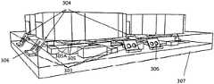
- FIG. 6illustrates internal construction details of another example of an mCoP module package with mechanically compliant internal leadframes 303 that may form electrical and/or thermal pathways for externally attached component connections 304 .
- the examplemay be the same as the example shown in FIG. 5 .
- the mechanically compliant through-mold leadframesmay complete the electrical circuit from the substrate 307 up to the components and may provide additional thermal and/or electrical connections 305 for internal components 305 A.
- One or more of the leadframesmay also contain openings 306 that may be circular, oval, rectangular or any other shape. These openings 306 may improve plastic mold compound flow during the molding process and/or mold compound interlocking.
- FIG. 7illustrates an external view of another example of a multiple components-on-package (mCoP) device 400 that may have multiple active and/or passive components 402 attached to the top of a module package 400 .
- the mCoP Module package 400may be a fully molded electrical circuit with internal leadframes that form exposed pads 401 for electrical and/or thermal connections to one or more externally attached components 402 .
- FIGS. 7 and 8show an example of an mCoP device with multiple active and/or passive components attached to the top surface of the module package.
- This devicemay require more complex leadframe designs and/or post-mold processing and/or post-mold machining, but may provide all the same functional characteristics as previously disclosed herein.
- the mechanically compliant internal leadframesmay provide electrically and/or thermally conductive pathways that distribute between the internal components and circuit within the module and the attached external components. Angular bends may be at precise locations and may act to decouple and redistribute any downward force due to assembly and mold packing pressures that might otherwise damage the substrate and/or attached components.
- the openings in the leadframemay be circular, oval, rectangular, or any other shape and may facilitate mold locking, mold flow, and/or minimize mold voids and/or prevent large areas of delamination.
- the leadframemay also have a multiplicity of areas along the length on each side containing thinned regions, typically half the thickness being removed by machining and/or etching. These half-etch features may be provided at specific locations to further reduce the chance of delamination during subsequent reflows and other reliability related concerns.
- internal leadframescould be used to redistribute electrical signals within the module package, effectively providing an additional signal layer between components. These internal leadframes would not necessarily require exposure to the top surface of the package. These leadframes could be considered to be intermediate conductive layers that could act to bridge electrical signals from components at one side of the package and extend over many internal components to make high current connections to other components at the other side of the package. Leadframes forming internal connections from the backside of flip chip silicon die to other internal components would be one example. Connecting vertical FET's together and to the substrate would be another. Another example would be a leadframe spanning the entire distance of the package length to provide electrical and thermal connections for any number of components.
- Variations of what have been describedmay include a variety of attach methods to the substrate, internal components, and/or external components. These methods may include but are not limited to epoxy, solder, and/or any adhesive that is either conductive or non-conductive to heat and/or electricity.
- the internal leadframemay include any multiple of leadframes and/or structures that may form conductive pathways for relevant operation of the package. Leadframe structures may connect/attach to interposers, clips, metallic stand-offs, and/or any variation of material structure capable of providing a conductive pathway for heat and/or electricity.
- Externally mounted/attached componentsmay include but are not limited to passive components, active components, and/or any variation of thermally and/or electrically conductive material to include heat sinking devices, heat pipes, intercoolers, and/or externally attached Peltier and/or energy harvesting and control devices.
- Relational terms such as “first” and “second” and the likemay be used solely to distinguish one entity or action from another, without necessarily requiring or implying any actual relationship or order between them.
- the terms “comprises,” “comprising,” and any other variation thereof when used in connection with a list of elements in the specification or claimsare intended to indicate that the list is not exclusive and that other elements may be included.
- an element proceeded by an “a” or an “an”does not, without further constraints, preclude the existence of additional elements of the identical type.
Landscapes
- Engineering & Computer Science (AREA)
- Microelectronics & Electronic Packaging (AREA)
- Physics & Mathematics (AREA)
- Condensed Matter Physics & Semiconductors (AREA)
- General Physics & Mathematics (AREA)
- Computer Hardware Design (AREA)
- Power Engineering (AREA)
- Manufacturing & Machinery (AREA)
- Lead Frames For Integrated Circuits (AREA)
- Structures Or Materials For Encapsulating Or Coating Semiconductor Devices Or Solid State Devices (AREA)
Abstract
Description
Claims (16)
Priority Applications (1)
| Application Number | Priority Date | Filing Date | Title |
|---|---|---|---|
| US16/095,276US11272618B2 (en) | 2016-04-26 | 2017-04-11 | Mechanically-compliant and electrically and thermally conductive leadframes for component-on-package circuits |
Applications Claiming Priority (3)
| Application Number | Priority Date | Filing Date | Title |
|---|---|---|---|
| US201662327875P | 2016-04-26 | 2016-04-26 | |
| US16/095,276US11272618B2 (en) | 2016-04-26 | 2017-04-11 | Mechanically-compliant and electrically and thermally conductive leadframes for component-on-package circuits |
| PCT/US2017/027047WO2017189224A1 (en) | 2016-04-26 | 2017-04-11 | Mechanically-compliant and electrically and thermally conductive leadframes for component-on-package circuits |
Publications (2)
| Publication Number | Publication Date |
|---|---|
| US20190141834A1 US20190141834A1 (en) | 2019-05-09 |
| US11272618B2true US11272618B2 (en) | 2022-03-08 |
Family
ID=58610047
Family Applications (2)
| Application Number | Title | Priority Date | Filing Date |
|---|---|---|---|
| US16/095,276ActiveUS11272618B2 (en) | 2016-04-26 | 2017-04-11 | Mechanically-compliant and electrically and thermally conductive leadframes for component-on-package circuits |
| US15/495,405AbandonedUS20170311447A1 (en) | 2016-04-26 | 2017-04-24 | Mechanically-compliant and electrically and thermally conductive leadframes for component-on-package circuits |
Family Applications After (1)
| Application Number | Title | Priority Date | Filing Date |
|---|---|---|---|
| US15/495,405AbandonedUS20170311447A1 (en) | 2016-04-26 | 2017-04-24 | Mechanically-compliant and electrically and thermally conductive leadframes for component-on-package circuits |
Country Status (5)
| Country | Link |
|---|---|
| US (2) | US11272618B2 (en) |
| EP (1) | EP3449502B1 (en) |
| CN (1) | CN109075151B (en) |
| TW (1) | TWI681523B (en) |
| WO (1) | WO2017189224A1 (en) |
Cited By (2)
| Publication number | Priority date | Publication date | Assignee | Title |
|---|---|---|---|---|
| US11749576B2 (en) | 2018-03-27 | 2023-09-05 | Analog Devices International Unlimited Company | Stacked circuit package with molded base having laser drilled openings for upper package |
| US11844178B2 (en) | 2020-06-02 | 2023-12-12 | Analog Devices International Unlimited Company | Electronic component |
Families Citing this family (4)
| Publication number | Priority date | Publication date | Assignee | Title |
|---|---|---|---|---|
| CN109075151B (en) | 2016-04-26 | 2023-06-27 | 亚德诺半导体国际无限责任公司 | Lead frame for mechanical mating, and electrical and thermal conduction of component package circuits |
| US11410977B2 (en) | 2018-11-13 | 2022-08-09 | Analog Devices International Unlimited Company | Electronic module for high power applications |
| JP7211267B2 (en)* | 2019-05-29 | 2023-01-24 | 株式会社デンソー | Semiconductor package manufacturing method |
| US20230253299A1 (en)* | 2022-02-10 | 2023-08-10 | Advanced Semiconductor Engineering, Inc. | Electronic package |
Citations (297)
| Publication number | Priority date | Publication date | Assignee | Title |
|---|---|---|---|---|
| US4089041A (en) | 1975-08-07 | 1978-05-09 | Amp Incorporated | Circuit programming device |
| JPS59155154A (en) | 1983-02-23 | 1984-09-04 | Nec Corp | Semiconductor device |
| US4739125A (en)* | 1985-09-27 | 1988-04-19 | Hitachi, Ltd. | Electric component part having lead terminals |
| US4914259A (en) | 1987-09-08 | 1990-04-03 | The Furukawa Electric Co., Ltd. | Molded circuit board |
| US5343075A (en) | 1991-06-29 | 1994-08-30 | Sony Corporation | Composite stacked semiconductor device with contact plates |
| US5485037A (en)* | 1993-04-12 | 1996-01-16 | Amkor Electronics, Inc. | Semiconductor device having a thermal dissipator and electromagnetic shielding |
| US5514907A (en) | 1995-03-21 | 1996-05-07 | Simple Technology Incorporated | Apparatus for stacking semiconductor chips |
| US5535101A (en) | 1992-11-03 | 1996-07-09 | Motorola, Inc. | Leadless integrated circuit package |
| US5647124A (en)* | 1994-04-25 | 1997-07-15 | Texas Instruments Incorporated | Method of attachment of a semiconductor slotted lead to a substrate |
| US5706172A (en) | 1995-08-16 | 1998-01-06 | Samsung Electronics Co., Ltd. | Stacked semiconductor package having supporting bars and a socket therefor |
| US20040262774A1 (en) | 2003-06-27 | 2004-12-30 | In-Ku Kang | Multi-chip packages having a plurality of flip chips and methods of manufacturing the same |
| US20050095835A1 (en) | 2003-09-26 | 2005-05-05 | Tessera, Inc. | Structure and method of making capped chips having vertical interconnects |
| US7129420B2 (en) | 2000-09-05 | 2006-10-31 | Seiko Epson Corporation | Semiconductor device and method for manufacture thereof, circuit board, and electronic instrument |
| US20070114352A1 (en)* | 2005-11-18 | 2007-05-24 | Victor R Cruz Erwin | Semiconductor die package using leadframe and clip and method of manufacturing |
| US20070222044A1 (en)* | 2006-03-21 | 2007-09-27 | Ralf Otremba | Electronic Component and Methods to Produce an Electronic Component |
| US20070246806A1 (en) | 2006-04-19 | 2007-10-25 | Stats Chippac Ltd. | Embedded integrated circuit package system |
| US20070262346A1 (en)* | 2006-05-10 | 2007-11-15 | Ralf Otremba | Electronic Component and a Method for its Production |
| US20070273049A1 (en) | 2006-05-12 | 2007-11-29 | Broadcom Corporation | Interconnect structure and formation for package stacking of molded plastic area array package |
| US20080128890A1 (en) | 2006-11-30 | 2008-06-05 | Advanced Semiconductor Engineering, Inc. | Chip package and fabricating process thereof |
| US20100013064A1 (en) | 2008-07-21 | 2010-01-21 | Chain-Hau Hsu | Semiconductor device packages with electromagnetic interference shielding |
| US7683473B2 (en) | 2005-09-28 | 2010-03-23 | Spansion Llc | Semiconductor device, fabrication method therefor, and film fabrication method |
| US20100133674A1 (en) | 2008-12-01 | 2010-06-03 | Francois Hebert | Compact Semiconductor Package with Integrated Bypass Capacitor and Method |
| WO2010067508A1 (en) | 2008-12-12 | 2010-06-17 | 株式会社村田製作所 | Multilayer substrate and method for manufacturing same |
| US7838334B2 (en) | 2008-12-01 | 2010-11-23 | Advanced Semiconductor Engineering, Inc. | Package-on-package device, semiconductor package and method for manufacturing the same |
| US20110013349A1 (en) | 2008-03-31 | 2011-01-20 | Murata Manufacturing Co., Ltd. | Electronic component module and method of manufacturing the electronic component module |
| US20110115060A1 (en) | 2009-11-19 | 2011-05-19 | Advanced Semiconductor Engineering, Inc. | Wafer-Level Semiconductor Device Packages with Electromagnetic Interference Shielding |
| US7982139B2 (en)* | 2003-12-05 | 2011-07-19 | Ibiden Co. Ltd. | Multilayer printed wiring board |
| US20110177654A1 (en) | 2010-01-21 | 2011-07-21 | Advanced Semiconductor Engineering, Inc. | Wafer-Level Semiconductor Device Packages with Three-Dimensional Fan-Out and Manufacturing Methods Thereof |
| US20110241194A1 (en) | 2010-04-02 | 2011-10-06 | Advanced Semiconductor Engineering, Inc. | Stacked Semiconductor Device Package Assemblies with Reduced Wire Sweep and Manufacturing Methods Thereof |
| EP2381472A1 (en) | 2010-04-26 | 2011-10-26 | Commissariat à l'Énergie Atomique et aux Énergies Alternatives | Method for manufacturing a microelectronic device and microelectronic device thus manufactured |
| US20110292632A1 (en)* | 2010-05-26 | 2011-12-01 | Yenting Wen | Method for manufacturing a semiconductor component and structure therefor |
| US20120025227A1 (en) | 2010-07-30 | 2012-02-02 | Cree Hong Kong, Ltd. | Water resistant surface mount device package |
| US20120074532A1 (en) | 2010-09-27 | 2012-03-29 | Advanced Semiconductor Engineering, Inc. | Semiconductor package with integrated metal pillars and manufacturing methods thereof |
| US8193034B2 (en) | 2006-11-10 | 2012-06-05 | Stats Chippac, Ltd. | Semiconductor device and method of forming vertical interconnect structure using stud bumps |
| US20120139122A1 (en)* | 2010-12-02 | 2012-06-07 | Sony Corporation | Semiconductor device and manufacturing method thereof |
| US8203164B2 (en) | 2007-03-14 | 2012-06-19 | Samsung Led Co., Ltd. | Light emitting diode package |
| US20120181689A1 (en) | 2008-12-08 | 2012-07-19 | Stats Chippac, Ltd. | Semiconductor Device and Method of Forming Bond Wires and Stud Bumps in Recessed Region of Peripheral Area around the Device for Electrical Interconnection to Other Devices |
| US8241956B2 (en) | 2010-03-08 | 2012-08-14 | Stats Chippac, Ltd. | Semiconductor device and method of forming wafer level multi-row etched lead package |
| US8258010B2 (en) | 2009-03-17 | 2012-09-04 | Stats Chippac, Ltd. | Making a semiconductor device having conductive through organic vias |
| US20120223428A1 (en) | 2006-09-22 | 2012-09-06 | Stats Chippac, Ltd. | Semiconductor Device and Method of Forming Vertical Interconnect Structure Between Semiconductor Die and Substrate |
| US8283750B2 (en) | 2006-05-02 | 2012-10-09 | Ipdia | Electronic device having electrode with high area density and improved mechanical stability |
| US20120273960A1 (en) | 2011-04-30 | 2012-11-01 | Stats Chippac, Ltd. | Semiconductor Device and Method of Embedding TSV Semiconductor Die Within Encapsulant with TMV for Vertical Interconnect in POP |
| US8349721B2 (en) | 2008-03-19 | 2013-01-08 | Stats Chippac, Ltd. | Semiconductor device and method of forming insulating layer on conductive traces for electrical isolation in fine pitch bonding |
| US8349657B2 (en) | 2008-12-10 | 2013-01-08 | Stats Chippac, Ltd. | Semiconductor device and method of forming conductive pillars in recessed region of peripheral area around the device for electrical interconnection to other devices |
| US20130015569A1 (en) | 2011-07-12 | 2013-01-17 | Great Wall Semiconductor Corporation | Semiconductor Device and Method of Forming Substrate With Seated Plane for Mating With Bumped Semiconductor Die |
| US8383457B2 (en) | 2010-09-03 | 2013-02-26 | Stats Chippac, Ltd. | Semiconductor device and method of forming interposer frame over semiconductor die to provide vertical interconnect |
| US8409922B2 (en) | 2010-09-14 | 2013-04-02 | Stats Chippac, Ltd. | Semiconductor device and method of forming leadframe interposer over semiconductor die and TSV substrate for vertical electrical interconnect |
| US8445990B2 (en) | 2010-12-10 | 2013-05-21 | Stats Chippac, Ltd. | Semiconductor device and method of forming an inductor within interconnect layer vertically separated from semiconductor die |
| US8502387B2 (en) | 2010-12-09 | 2013-08-06 | Stats Chippac Ltd. | Integrated circuit packaging system with vertical interconnection and method of manufacture thereof |
| US20130200527A1 (en) | 2010-09-03 | 2013-08-08 | Stats Chippac, Ltd. | Semiconductor Device and Method of Forming Pre-Molded Substrate to Reduce Warpage During Die Molding |
| US8513812B2 (en) | 2009-09-11 | 2013-08-20 | Stats Chippac, Ltd. | Semiconductor device and method of forming integrated passive device |
| US20130214399A1 (en) | 2011-06-27 | 2013-08-22 | National Semiconductor Corporation | DC/DC Converter Power Module Package Incorporating a Stacked Controller and Construction Methodology |
| US8525344B2 (en) | 2011-02-24 | 2013-09-03 | Stats Chippac, Ltd. | Semiconductor device and method of forming bond wires between semiconductor die contact pads and conductive TOV in peripheral area around semiconductor die |
| US8525340B2 (en) | 2010-06-11 | 2013-09-03 | Premitec, Inc. | Flexible electronic devices and related methods |
| US8530274B2 (en) | 2010-02-03 | 2013-09-10 | Stats Chippac, Ltd. | Semiconductor device and method of forming air gap adjacent to stress sensitive region of the die |
| US20130234324A1 (en) | 2010-08-17 | 2013-09-12 | Stats Chippac, Ltd. | Semiconductor Device and Method of Forming Vertically Offset Conductive Pillars Over First Substrate Aligned to Vertically Offset BOT Interconnect Sites Formed Over Second Substrate |
| US20130249051A1 (en)* | 2012-03-23 | 2013-09-26 | Texas Instruments Incorporated | Packaged Semiconductor Device Having Multilevel Leadframes Configured as Modules |
| US8563418B2 (en) | 2010-03-09 | 2013-10-22 | Stats Chippac, Ltd. | Semiconductor device and method of forming vertically offset bond on trace interconnects on different height traces |
| US8569882B2 (en) | 2011-03-24 | 2013-10-29 | Stats Chippac Ltd. | Integrated circuit packaging system with collapsed multi-integration package and method of manufacture thereof |
| US8581381B2 (en) | 2006-06-20 | 2013-11-12 | Broadcom Corporation | Integrated circuit (IC) package stacking and IC packages formed by same |
| US20130299971A1 (en) | 2010-11-02 | 2013-11-14 | Stats Chippac, Ltd. | Semiconductor Device and Method of Forming Penetrable Film Encapsulant Around Semiconductor Die and Interconnect Structure |
| US20130341786A1 (en) | 2012-06-25 | 2013-12-26 | Taiwan Semiconductor Manufacturing Company, Ltd. | Package on Package Devices and Methods of Packaging Semiconductor Dies |
| US8623702B2 (en) | 2011-02-24 | 2014-01-07 | Stats Chippac, Ltd. | Semiconductor device and method of forming conductive THV and RDL on opposite sides of semiconductor die for RDL-to-RDL bonding |
| US8624374B2 (en) | 2010-04-02 | 2014-01-07 | Advanced Semiconductor Engineering, Inc. | Semiconductor device packages with fan-out and with connecting elements for stacking and manufacturing methods thereof |
| US8674516B2 (en) | 2011-06-22 | 2014-03-18 | Stats Chippac Ltd. | Integrated circuit packaging system with vertical interconnects and method of manufacture thereof |
| US20140110860A1 (en) | 2009-11-04 | 2014-04-24 | Stats Chippac, Ltd. | Semiconductor Package and Method of Mounting Semiconductor Die to Opposite Sides of TSV Substrate |
| US20140124919A1 (en) | 2012-11-07 | 2014-05-08 | Advanced Semiconductor Engineering, Inc. | Semiconductor device and semiconductor process |
| US20140138807A1 (en) | 2011-08-16 | 2014-05-22 | General Electric Company | Power overlay structure with leadframe connections |
| US20140145319A1 (en) | 2012-11-26 | 2014-05-29 | Infineon Technologies Dresden Gmbh | Semicondutor Packages and Methods of Fabrication Thereof |
| US20140154843A1 (en) | 2008-12-01 | 2014-06-05 | Alpha and Omega Semiconductor Incorprated | Method for Top-side Cooled Semiconductor Package with Stacked Interconnection Plates |
| US20140151880A1 (en) | 2011-08-19 | 2014-06-05 | Marvell World Trade Ltd. | Package-on-package structures |
| US20140159251A1 (en) | 2012-12-11 | 2014-06-12 | Stats Chippac, Ltd. | Semiconductor Device and Method of Forming Low Profile Fan-Out Package with Vertical Interconnection Units |
| US8790962B2 (en) | 2008-12-10 | 2014-07-29 | Stats Chippac, Ltd. | Semiconductor device and method of forming a shielding layer over a semiconductor die after forming a build-up interconnect structure |
| US8847369B2 (en) | 2012-07-20 | 2014-09-30 | Taiwan Semiconductor Manufacturing Company, Ltd. | Packaging structures and methods for semiconductor devices |
| US8853819B2 (en) | 2011-01-07 | 2014-10-07 | Advanced Semiconductor Engineering, Inc. | Semiconductor structure with passive element network and manufacturing method thereof |
| US20140312503A1 (en) | 2013-04-23 | 2014-10-23 | ByoungRim SEO | Semiconductor packages and methods of fabricating the same |
| US8877567B2 (en) | 2010-11-18 | 2014-11-04 | Stats Chippac, Ltd. | Semiconductor device and method of forming uniform height insulating layer over interposer frame as standoff for semiconductor die |
| US20140361423A1 (en) | 2011-06-03 | 2014-12-11 | Stats Chippac, Ltd. | Semiconductor Device and Method of Using Leadframe Bodies to Form Openings Through Encapsulant for Vertical Interconnect of Semiconductor Die |
| US8932908B2 (en) | 2010-11-22 | 2015-01-13 | Stats Chippac, Ltd. | Semiconductor device and method of forming partially-etched conductive layer recessed within substrate for bonding to semiconductor die |
| US8941222B2 (en) | 2010-11-11 | 2015-01-27 | Advanced Semiconductor Engineering Inc. | Wafer level semiconductor package and manufacturing methods thereof |
| US20150061095A1 (en) | 2013-08-29 | 2015-03-05 | Mi-Na Choi | Package-on-package devices, methods of fabricating the same, and semiconductor packages |
| US8987734B2 (en) | 2013-03-15 | 2015-03-24 | Advanced Semiconductor Engineering, Inc. | Semiconductor wafer, semiconductor process and semiconductor package |
| US20150084206A1 (en) | 2013-09-24 | 2015-03-26 | Stats Chippac, Ltd. | Semiconductor Device and Method of Forming Dual Fan-Out Semiconductor Package |
| US9006099B2 (en) | 2011-06-08 | 2015-04-14 | Great Wall Semiconductor Corporation | Semiconductor device and method of forming a power MOSFET with interconnect structure silicide layer and low profile bump |
| US9029193B2 (en) | 2008-12-10 | 2015-05-12 | Stats Chippac, Ltd. | Semiconductor device and method of forming an interconnect structure for 3-D devices using encapsulant for structural support |
| US9054083B2 (en) | 2009-06-08 | 2015-06-09 | Stats Chippac, Ltd. | Semiconductor device and method of making TSV interconnect structures using encapsulant for structural support |
| US9059186B2 (en) | 2008-07-14 | 2015-06-16 | Stats Chippac, Ltd. | Embedded semiconductor die package and method of making the same using metal frame carrier |
| US20150179570A1 (en) | 2013-12-23 | 2015-06-25 | Stats Chippac, Ltd. | Semiconductor Device and Method of Forming Fine Pitch RDL Over Semiconductor Die in Fan-Out Package |
| US20150179626A1 (en) | 2013-07-31 | 2015-06-25 | Alpha And Omega Semiconductor Incorporated | Method of making stacked multi-chip packaging structure |
| US20150187710A1 (en) | 2011-12-30 | 2015-07-02 | Deca Technologies Inc. | Semiconductor device and method comprising thickened redistribution layers |
| US9082780B2 (en) | 2012-03-23 | 2015-07-14 | Stats Chippac, Ltd. | Semiconductor device and method of forming a robust fan-out package including vertical interconnects and mechanical support layer |
| US9105532B2 (en) | 2011-06-23 | 2015-08-11 | Stats Chippac, Ltd. | Semiconductor device and method of forming interconnect structure over seed layer on contact pad of semiconductor die without undercutting seed layer beneath interconnect structure |
| US9117812B2 (en) | 2012-03-09 | 2015-08-25 | Stats Chippac, Ltd. | Semiconductor device and method of forming non-linear interconnect layer with extended length for joint reliability |
| US9129980B2 (en) | 2011-03-03 | 2015-09-08 | Broadcom Corporation | Package 3D interconnection and method of making same |
| US20150255360A1 (en) | 2014-03-05 | 2015-09-10 | Siliconware Precision Industries Co., Ltd. | Package on package structure and fabrication method thereof |
| US9142515B2 (en) | 2010-07-16 | 2015-09-22 | Stats Chippac, Ltd. | Semiconductor device with protective layer over exposed surfaces of semiconductor die |
| CN104934391A (en) | 2014-03-18 | 2015-09-23 | 日月光半导体制造股份有限公司 | Semiconductor device and semiconductor process |
| US20150279815A1 (en) | 2014-03-28 | 2015-10-01 | Stats Chippac, Ltd. | Semiconductor Device and Method of Forming Substrate Having Conductive Columns |
| US20150279778A1 (en) | 2014-03-28 | 2015-10-01 | Stats Chippac, Ltd. | Semiconductor Device and Method of Forming RDL and Vertical Interconnect by Laser Direct Structuring |
| US9171792B2 (en) | 2011-02-28 | 2015-10-27 | Advanced Semiconductor Engineering, Inc. | Semiconductor device packages having a side-by-side device arrangement and stacking functionality |
| US9177832B2 (en) | 2011-09-16 | 2015-11-03 | Stats Chippac, Ltd. | Semiconductor device and method of forming a reconfigured stackable wafer level package with vertical interconnect |
| US20150325516A1 (en) | 2014-05-09 | 2015-11-12 | Siliconware Precision Industries Co., Ltd. | Coreless packaging substrate, pop structure, and methods for fabricating the same |
| US20150325509A1 (en) | 2014-05-09 | 2015-11-12 | Qualcomm Incorporated | SUBSTRATE BLOCK FOR PoP PACKAGE |
| US9236332B2 (en) | 2010-06-24 | 2016-01-12 | Stats Chippac, Ltd. | Semiconductor device and method of forming vertically offset bond on trace interconnect structure on leadframe |
| US9236352B2 (en) | 2009-03-13 | 2016-01-12 | Stats Chippac, Ltd. | Semiconductor die and method of forming noise absorbing regions between THVs in peripheral region of the die |
| US9240331B2 (en) | 2012-12-20 | 2016-01-19 | Stats Chippac, Ltd. | Semiconductor device and method of making bumpless flipchip interconnect structures |
| US9245834B2 (en) | 2012-03-16 | 2016-01-26 | Stats Chippac, Ltd. | Semiconductor device and method of forming compliant conductive interconnect structure in flipchip package |
| US20160035656A1 (en) | 2013-03-15 | 2016-02-04 | Invensas Corporation | RECONFIGURABLE PoP |
| US9257411B2 (en) | 2010-05-13 | 2016-02-09 | Stats Chippac, Ltd. | Semiconductor device and method of embedding bumps formed on semiconductor die into penetrable adhesive layer to reduce die shifting during encapsulation |
| US9257356B2 (en) | 2008-12-10 | 2016-02-09 | Stats Chippac, Ltd. | Semiconductor device and method of forming an IPD beneath a semiconductor die with direct connection to external devices |
| US9269595B2 (en) | 2010-01-29 | 2016-02-23 | Stats Chippac, Ltd. | Semiconductor device with thin profile WLCSP with vertical interconnect over package footprint |
| US9275877B2 (en) | 2011-09-20 | 2016-03-01 | Stats Chippac, Ltd. | Semiconductor device and method of forming semiconductor package using panel form carrier |
| US20160066406A1 (en) | 2014-09-03 | 2016-03-03 | Siliconware Precision Industries Co., Ltd. | Electronic module and fabrication method thereof |
| US9281228B2 (en) | 2011-11-01 | 2016-03-08 | Stats Chippac, Ltd. | Semiconductor device and method of forming thermal interface material and heat spreader over semiconductor die |
| US20160071831A1 (en) | 2014-09-05 | 2016-03-10 | Baik-Woo Lee | Semiconductor package |
| US9299650B1 (en) | 2013-09-25 | 2016-03-29 | Stats Chippac Ltd. | Integrated circuit packaging system with single metal layer interposer and method of manufacture thereof |
| US9324659B2 (en) | 2011-08-01 | 2016-04-26 | Stats Chippac, Ltd. | Semiconductor device and method of forming POP with stacked semiconductor die and bumps formed directly on the lower die |
| US9331002B2 (en) | 2008-05-27 | 2016-05-03 | Stats Chippac, Ltd. | Semiconductor device and method of forming through vias with reflowed conductive material |
| US20160126176A1 (en) | 2014-11-03 | 2016-05-05 | Siliconware Precision Industries Co., Ltd. | Package substrate, package structure and fabrication method thereof |
| US9337116B2 (en) | 2010-10-28 | 2016-05-10 | Stats Chippac, Ltd. | Semiconductor device and method of forming stepped interposer for stacking and electrically connecting semiconductor die |
| US20160150632A1 (en) | 2014-11-21 | 2016-05-26 | Freescale Semiconductor, Inc. | Packaged electronic devices with top terminations, and methods of manufacture thereof |
| US9373578B2 (en) | 2011-05-31 | 2016-06-21 | STATS ChipPAC Pte. Ltd. | Semiconductor device and method of forming interconnect structure with conductive pads having expanded interconnect surface area for enhanced interconnection properties |
| US9379064B2 (en) | 2009-08-14 | 2016-06-28 | STATS ChipPAC Pte. Ltd. | Semiconductor device and method of mounting semiconductor die to heat spreader on temporary carrier and forming polymer layer and conductive layer over the die |
| US9378983B2 (en) | 2011-05-03 | 2016-06-28 | STATS ChipPAC Pte. Ltd. | Semiconductor device and method of mounting cover to semiconductor die and interposer with adhesive material |
| US9390945B2 (en) | 2012-05-08 | 2016-07-12 | STATS ChipPAC Pte. Ltd. | Semiconductor device and method of depositing underfill material with uniform flow rate |
| US9391046B2 (en) | 2011-05-20 | 2016-07-12 | STATS ChipPAC Pte. Ltd. | Semiconductor device and method of forming 3D semiconductor package with semiconductor die stacked over semiconductor wafer |
| US9397074B1 (en) | 2015-04-29 | 2016-07-19 | Advanced Semiconductor Engineering, Inc. | Semiconductor device package and method of manufacturing the same |
| US9401347B2 (en) | 2009-10-23 | 2016-07-26 | STATS ChipPAC Pte. Ltd. | Semiconductor device and method of forming a shielding layer over a semiconductor die disposed in a cavity of an interconnect structure and grounded through the die TSV |
| US9406636B2 (en) | 2013-09-11 | 2016-08-02 | Broadcom Corporation | Interposer package-on-package structure |
| US9406658B2 (en) | 2010-12-17 | 2016-08-02 | Advanced Semiconductor Engineering, Inc. | Embedded component device and manufacturing methods thereof |
| US9406579B2 (en) | 2012-05-14 | 2016-08-02 | STATS ChipPAC Pte. Ltd. | Semiconductor device and method of controlling warpage in semiconductor package |
| US9406552B2 (en) | 2012-12-20 | 2016-08-02 | Advanced Semiconductor Engineering, Inc. | Semiconductor device having conductive via and manufacturing process |
| US20160276256A1 (en) | 2015-03-17 | 2016-09-22 | Siliconware Precision Industries Co., Ltd. | Electronic package and fabrication method thereof and substrate structure |
| US20160284642A1 (en) | 2013-12-23 | 2016-09-29 | Sanka Ganesan | Package on package architecture and method for making |
| US20160307799A1 (en) | 2015-04-15 | 2016-10-20 | Advanced Semiconductor Engineering, Inc. | Semiconductor substrates, semiconductor packages and processes of making the same |
| US9478486B2 (en) | 2008-12-11 | 2016-10-25 | STATS ChipPAC Pte. Ltd. | Semiconductor device and method of forming topside and bottom-side interconnect structures around core die with TSV |
| US9484259B2 (en) | 2011-09-21 | 2016-11-01 | STATS ChipPAC Pte. Ltd. | Semiconductor device and method of forming protection and support structure for conductive interconnect structure |
| US20160322343A1 (en) | 2015-04-29 | 2016-11-03 | Deca Technologies Inc. | 3d interconnect component for fully molded packages |
| US20160329272A1 (en) | 2014-12-19 | 2016-11-10 | Intel IP Corporation | Stacked semiconductor device package with improved interconnect bandwidth |
| US9502335B2 (en) | 2014-05-08 | 2016-11-22 | Siliconware Precision Industries Co., Ltd. | Package structure and method for fabricating the same |
| US20160343651A1 (en) | 2015-05-22 | 2016-11-24 | Qualcomm Incorporated | System, apparatus, and method for embedding a 3d component with an interconnect structure |
| US9508626B2 (en) | 2010-04-23 | 2016-11-29 | STATS ChipPAC Pte. Ltd. | Semiconductor device and method of forming openings in thermally-conductive frame of FO-WLCSP to dissipate heat and reduce package height |
| US20170011936A1 (en) | 2012-10-02 | 2017-01-12 | STATS ChipPAC Pte. Ltd. | Semiconductor Device and Method of Depositing Encapsulant Along Sides and Surface Edge of Semiconductor Die in Embedded WLCSP |
| US9559043B2 (en) | 2013-12-06 | 2017-01-31 | Silergy Semiconductor Technology (Hangzhou) Ltd. | Multi-level leadframe with interconnect areas for soldering conductive bumps, multi-level package assembly and method for manufacturing the same |
| US9570381B2 (en) | 2015-04-02 | 2017-02-14 | Advanced Semiconductor Engineering, Inc. | Semiconductor packages and related manufacturing methods |
| US20170062120A1 (en) | 2015-08-31 | 2017-03-02 | Qualcomm Incorporated | Substrate comprising an embedded inductor and a thin film magnetic core |
| US9589910B2 (en) | 2010-09-02 | 2017-03-07 | STATS ChipPAC Pte. Ltd. | Semiconductor device and method of forming base leads from base substrate as standoff for stacking semiconductor die |
| US20170077364A1 (en) | 2015-09-11 | 2017-03-16 | Epistar Corporation | Light-emitting device and manufacturing method thereof |
| US20170077039A1 (en) | 2015-09-10 | 2017-03-16 | Advanced Semiconductor Engineering, Inc. | Semiconductor package device and method of manufacturing the same |
| US9601369B2 (en) | 2009-06-12 | 2017-03-21 | STATS ChipPAC Pte. Ltd. | Semiconductor device and method of forming conductive vias with trench in saw street |
| US9613912B2 (en) | 2014-12-16 | 2017-04-04 | Deca Technologies Inc. | Method of marking a semiconductor package |
| US20170098610A1 (en) | 2012-09-17 | 2017-04-06 | STATS ChipPAC Pte. Ltd. | Semiconductor Device and Method of Using Substrate Having Base and Conductive Posts to Form Vertical Interconnect Structure in Embedded Die Package |
| US20170110392A1 (en) | 2015-10-15 | 2017-04-20 | Advanced Semiconductor Engineering, Inc. | Semiconductor package structure and method for manufacturing the same structure |
| US9653407B2 (en) | 2015-07-02 | 2017-05-16 | Advanced Semiconductor Engineering, Inc. | Semiconductor device packages |
| US20170148746A1 (en) | 2015-11-19 | 2017-05-25 | Advanced Semiconductor Engineering, Inc. | Semiconductor device package |
| US20170162476A1 (en) | 2015-12-03 | 2017-06-08 | Infineon Technologies Ag | Connector block with two sorts of through connections, and electronic device comprising a connector block |
| US9679881B2 (en) | 2010-02-03 | 2017-06-13 | STATS ChipPAC Pte. Ltd. | Semiconductor device and method of forming cavity adjacent to sensitive region of semiconductor die using wafer-level underfill material |
| US20170179048A1 (en) | 2009-12-07 | 2017-06-22 | Intersil Americas LLC | Stacked inductor-electronic package assembly and technique for manufacturing same |
| US20170179041A1 (en) | 2015-12-22 | 2017-06-22 | Intel Corporation | Semiconductor package with trenched molding-based electromagnetic interference shielding |
| US20170186702A1 (en) | 2015-12-28 | 2017-06-29 | Siliconware Precision Industries Co., Ltd. | Packaging substrate and electronic package having the same |
| US20170221858A1 (en) | 2015-11-30 | 2017-08-03 | Taiwan Semiconductor Manufacturing Company, Ltd. | Tri-Layer CoWoS Structure |
| US9729059B1 (en) | 2016-02-09 | 2017-08-08 | Faraday Semi, LLC | Chip embedded DC-DC converter |
| US20170250172A1 (en) | 2016-02-29 | 2017-08-31 | Semtech Corporation | Semiconductor Device and Method of Stacking Semiconductor Die for System-Level ESD Protection |
| US9754868B2 (en) | 2015-12-31 | 2017-09-05 | Siliconware Precision Industries Co., Ltd. | Substrate structure, electronic package and method for fabricating the electronic package |
| US20170256481A1 (en) | 2016-03-04 | 2017-09-07 | Siliconware Precision Industries Co., Ltd. | Electronic package and semiconductor substrate |
| EP3217774A1 (en) | 2016-03-08 | 2017-09-13 | ABB Schweiz AG | Semiconductor module |
| US9768144B2 (en) | 2010-02-03 | 2017-09-19 | Marvell World Trade Ltd. | Package assembly including a semiconductor substrate in which a first portion of a surface of the semiconductor substrate is recessed relative to a second portion of the surface of the semiconductor substrate to form a recessed region in the semiconductor substrate |
| US20170278807A1 (en) | 2016-03-28 | 2017-09-28 | Siliconware Precision Industries Co., Ltd. | Electronic package with antenna structure |
| US9799621B2 (en) | 2012-03-20 | 2017-10-24 | STATS ChipPAC Pte. Ltd. | Semiconductor device and method of forming duplex plated bump-on-lead pad over substrate for finer pitch between adjacent traces |
| US20170311447A1 (en)* | 2016-04-26 | 2017-10-26 | Linear Technology Corporation | Mechanically-compliant and electrically and thermally conductive leadframes for component-on-package circuits |
| US9824923B2 (en) | 2011-10-17 | 2017-11-21 | STATS ChipPAC Pte. Ltd. | Semiconductor device and method of forming conductive pillar having an expanded base |
| US9842808B2 (en) | 2010-08-10 | 2017-12-12 | STATS ChipPAC Pte. Ltd. | Semiconductor device and method of forming vertical interconnect in FO-WLCSP using leadframe disposed between semiconductor die |
| US9847324B2 (en) | 2008-12-12 | 2017-12-19 | STATS ChipPAC Pte. Ltd. | Semiconductor device and method of forming a vertical interconnect structure for 3-D FO-WLCSP |
| US20180052281A1 (en) | 2016-08-16 | 2018-02-22 | Advanced Semiconductor Engineering, Inc. | Substrate, semiconductor device and semiconductor package structure |
| US20180061815A1 (en) | 2016-08-31 | 2018-03-01 | Advanced Semiconductor Engineering, Inc. | Semiconductor package device and method of manufacturing the same |
| US20180068970A1 (en) | 2004-09-28 | 2018-03-08 | Rohm Co., Ltd. | Semiconductor device with a semiconductor chip connected in a flip chip manner |
| US20180068983A1 (en) | 2016-09-02 | 2018-03-08 | Siliconware Precision Industries Co., Ltd. | Electronic package and method for fabricating the same |
| US20180076165A1 (en) | 2016-09-14 | 2018-03-15 | International Business Machines Corporation | Method of forming solder bumps |
| US9922955B2 (en) | 2010-03-04 | 2018-03-20 | STATS ChipPAC Pte. Ltd. | Semiconductor device and method of forming package-on-package structure electrically interconnected through TSV in WLCSP |
| US9922917B2 (en) | 2014-12-19 | 2018-03-20 | Advanced Semiconductor Engineering, Inc. | Semiconductor package including substrates spaced by at least one electrical connecting element |
| US20180090466A1 (en) | 2016-09-29 | 2018-03-29 | Advanced Semiconductor Engineering, Inc. | Semiconductor device package and method of manufacturing the same |
| US20180102325A1 (en) | 2016-10-12 | 2018-04-12 | Advanced Semiconductor Engineering Korea, Inc. | Semiconductor package device and method of manufacturing the same |
| US9966335B2 (en) | 2010-11-16 | 2018-05-08 | STATS ChipPAC Pte. Ltd. | Semiconductor device and method of forming interposer frame electrically connected to embedded semiconductor die |
| US20180130774A1 (en) | 2016-11-10 | 2018-05-10 | Siliconware Precision Industries Co., Ltd. | Package stack structure |
| US20180138113A1 (en) | 2016-11-15 | 2018-05-17 | Advanced Semiconductor Engineering, Inc. | Semiconductor system and device package including interconnect structure |
| US20180138131A1 (en) | 2016-11-16 | 2018-05-17 | Tdk Corporation | Composite magnetic sealing material and electronic circuit package using the same |
| US9984993B2 (en) | 2015-02-13 | 2018-05-29 | Advanced Semiconductor Engineering, Inc. | Bonding structure for semiconductor package and method of manufacturing the same |
| US20180151485A1 (en) | 2016-11-28 | 2018-05-31 | Advanced Semiconductor Engineering, Inc. | Semiconductor device package including filling mold via |
| US9991193B2 (en) | 2016-06-15 | 2018-06-05 | Advanced Semiconductor Engineering, Inc. | Semiconductor device package |
| US20180158779A1 (en) | 2016-12-07 | 2018-06-07 | STATS ChipPAC Pte. Ltd. | Semiconductor Device and Method of Forming an Integrated SIP Module with Embedded Inductor or Package |
| US9997447B1 (en) | 2017-06-08 | 2018-06-12 | Advanced Ssemiconductor Engineering, Inc. | Semiconductor devices |
| US20180182704A1 (en) | 2016-12-23 | 2018-06-28 | Advanced Semiconductor Engineering, Inc. | Semiconductor package device and method of manufacturing the same |
| US10032652B2 (en) | 2014-12-05 | 2018-07-24 | Advanced Semiconductor Engineering, Inc. | Semiconductor package having improved package-on-package interconnection |
| US20180261551A1 (en) | 2017-03-13 | 2018-09-13 | STATS ChipPAC Pte. Ltd. | Semiconductor Device and Method of Forming Partition Fence and Shielding Layer Around Semiconductor Components |
| US20180269708A1 (en) | 2017-03-14 | 2018-09-20 | Advanced Semiconductor Engineering, Inc. | Semiconductor package device and method of manufacturing the same |
| US10096578B1 (en) | 2017-07-06 | 2018-10-09 | Advanced Semiconductor Engineering, Inc. | Semiconductor package device and method of manufacturing the same |
| US20180297834A1 (en) | 2014-11-10 | 2018-10-18 | AT & S Austria Technologies & Systemtechnik Aktiengesellschaft | MEMS Package |
| US10115661B2 (en) | 2013-02-08 | 2018-10-30 | Qualcomm Incorporated | Substrate-less discrete coupled inductor structure |
| US10115701B2 (en) | 2014-06-26 | 2018-10-30 | STATS ChipPAC Pte. Ltd. | Semiconductor device and method of forming conductive vias by backside via reveal with CMP |
| US20180331018A1 (en) | 2012-03-23 | 2018-11-15 | STATS ChipPAC Pte. Ltd. | Semiconductor Device and Method of Forming a Fan-Out PoP Device with PWB Vertical Interconnect Units |
| US20180331050A1 (en) | 2017-05-10 | 2018-11-15 | Advanced Semiconductor Engineering, Inc. | Semiconductor package device and method of manufacturing the same |
| US20180337130A1 (en) | 2017-05-16 | 2018-11-22 | Advanced Semiconductor Engineering, Inc. | Semiconductor package device and method of manufacturing the same |
| US20180342484A1 (en) | 2017-05-25 | 2018-11-29 | Siliconware Precision Industries Co., Ltd. | Electronic package and method for fabricating the same |
| US20180350766A1 (en) | 2011-05-03 | 2018-12-06 | Tessera, Inc. | Package-on-package assembly with wire bonds to encapsulation surface |
| US10157890B2 (en) | 2015-12-31 | 2018-12-18 | Taiwan Semiconductor Manufacturing Company Ltd. | Semiconductor structure and method of manufacturing the same |
| US10157887B2 (en) | 2017-03-09 | 2018-12-18 | Advanced Semiconductor Engineering, Inc. | Semiconductor device package and method of manufacturing the same |
| US10157821B1 (en) | 2017-05-30 | 2018-12-18 | Advanced Semiconductor Engineering, Inc. | Semiconductor packages |
| US10163876B2 (en) | 2016-05-31 | 2018-12-25 | Taiwan Semiconductor Manufacturing Company Ltd. | Semiconductor structure and manufacturing method thereof |
| US10163867B2 (en) | 2015-11-12 | 2018-12-25 | Amkor Technology, Inc. | Semiconductor package and manufacturing method thereof |
| US20180374798A1 (en) | 2017-06-24 | 2018-12-27 | Amkor Technology, Inc. | Semiconductor device having emi shielding structure and related methods |
| US20180374833A1 (en) | 2010-12-16 | 2018-12-27 | Intel Corporation | LOWER IC PACKAGE STRUCTURE FOR COUPLING WITH AN UPPER IC PACKAGE TO FORM A PACKAGE-ON-PACKAGE (PoP) ASSEMBLY AND PoP ASSEMBLY INCLUDING SUCH A LOWER IC PACKAGE STRUCTURE |
| US10177099B2 (en) | 2016-04-07 | 2019-01-08 | Advanced Semiconductor Engineering, Inc. | Semiconductor package structure, package on package structure and packaging method |
| US20190013301A1 (en) | 2017-07-04 | 2019-01-10 | Intel Corporation | Stacked dies with passive components within facing recesses |
| US20190019763A1 (en) | 2017-07-13 | 2019-01-17 | Mediatek Inc. | Semiconductor package including emi shielding structure and method for forming the same |
| US10186467B2 (en) | 2016-07-15 | 2019-01-22 | Advanced Semiconductor Engineering, Inc. | Semiconductor package device and method of manufacturing the same |
| US10193442B2 (en) | 2016-02-09 | 2019-01-29 | Faraday Semi, LLC | Chip embedded power converters |
| US10199320B2 (en) | 2014-12-05 | 2019-02-05 | Siliconware Precision Industries Co., Ltd. | Method of fabricating electronic package |
| US20190043819A1 (en) | 2017-08-02 | 2019-02-07 | Siliconware Precision Industries Co., Ltd. | Electronic package having redistribution structure |
| US20190051590A1 (en) | 2017-08-09 | 2019-02-14 | Advanced Semiconductor Engineering, Inc. | Semiconductor package device and method of manufacturing the same |
| US10211182B2 (en) | 2014-07-07 | 2019-02-19 | Intel IP Corporation | Package-on-package stacked microelectronic structures |
| US20190057940A1 (en) | 2016-03-16 | 2019-02-21 | Intel Corporation | Stairstep interposers with integrated shielding for electronics packages |
| US10224301B2 (en) | 2017-07-05 | 2019-03-05 | Advanced Semiconductor Engineering, Inc. | Semiconductor package device and method of manufacturing the same |
| US10229892B2 (en) | 2017-06-28 | 2019-03-12 | Advanced Semiconductor Engineering, Inc. | Semiconductor package and method for manufacturing a semiconductor package |
| US10229859B2 (en) | 2016-08-17 | 2019-03-12 | Advanced Semiconductor Engineering, Inc. | Semiconductor device package and a method of manufacturing the same |
| WO2019066987A1 (en) | 2017-09-30 | 2019-04-04 | Intel Corporation | Dimension tolerant multi-material stack |
| WO2019066986A1 (en) | 2017-09-30 | 2019-04-04 | Intel Corporation | Tsv-less die stacking using plated pillars/through mold interconnect |
| US10256173B2 (en) | 2016-02-22 | 2019-04-09 | Advanced Semiconductor Engineering, Inc. | Semiconductor device and method for manufacturing the same |
| US20190115319A1 (en) | 2016-01-27 | 2019-04-18 | Amkor Technology, Inc. | Semiconductor package and fabricating method thereof |
| US10269771B2 (en) | 2016-08-31 | 2019-04-23 | Advanced Semiconductor Engineering, Inc. | Semiconductor device package and a method of manufacturing the same |
| US10276382B2 (en) | 2016-08-11 | 2019-04-30 | Advanced Semiconductor Engineering, Inc. | Semiconductor device packages and stacked package assemblies including high density interconnections |
| US20190132983A1 (en) | 2017-11-02 | 2019-05-02 | At&S Austria Technologie & Systemtechnik Aktiengesellschaft | Component Carrier With Transistor Components Arranged Side By Side |
| US20190139846A1 (en) | 2017-11-03 | 2019-05-09 | Advanced Semiconductor Engineering, Inc. | Semiconductor device package and a method of manufacturing the same |
| US20190139946A1 (en) | 2017-11-03 | 2019-05-09 | Samsung Electronics Co., Ltd. | Package-on-package (pop) semiconductor package and electronic system including the same |
| US20190148304A1 (en) | 2017-11-11 | 2019-05-16 | At&S Austria Technologie & Systemtechnik Aktiengesellschaft | Embedding Known-Good Component in Known-Good Cavity of Known-Good Component Carrier Material With Pre-formed Electric Connection Structure |
| US10297519B2 (en) | 2015-03-17 | 2019-05-21 | STATS ChipPAC Pte. Ltd. | Semiconductor device and method of forming PoP semiconductor device with RDL over top package |
| US10297518B2 (en) | 2012-09-28 | 2019-05-21 | Stats Chippac, Ltd. | Semiconductor device and method of forming supporting layer over semiconductor die in thin fan-out wafer level chip scale package |
| US10325868B2 (en) | 2017-04-24 | 2019-06-18 | Advanced Semiconductor Engineering, Inc. | Semiconductor package device and method of manufacturing the same |
| US10332862B2 (en) | 2017-09-07 | 2019-06-25 | Advanced Semiconductor Engineering, Inc. | Semiconductor package structure and method for manufacturing the same |
| WO2019132965A1 (en) | 2017-12-29 | 2019-07-04 | Intel Corporation | Microelectronic assemblies |
| US20190206799A1 (en) | 2017-12-28 | 2019-07-04 | Intel IP Corporation | Face-up fan-out electronic package with passive components using a support |
| WO2019132963A1 (en) | 2017-12-29 | 2019-07-04 | Intel Corporation | Quantum computing assemblies |
| US10361150B2 (en) | 2017-03-15 | 2019-07-23 | Siliconware Precision Industries Co., Ltd. | Substrate construction and electronic package including the same |
| US20190237374A1 (en) | 2018-01-30 | 2019-08-01 | Siliconware Precision Industries Co., Ltd. | Electronic package and method for fabricating the same |
| US20190252305A1 (en) | 2018-02-09 | 2019-08-15 | Advanced Semiconductor Engineering, Inc. | Semiconductor device package and a method of manufacturing the same |
| US10388598B2 (en) | 2016-06-09 | 2019-08-20 | Advanced Semiconductor Engineering, Inc. | Interposer, semiconductor package structure, and semiconductor process |
| US10403609B2 (en) | 2015-12-21 | 2019-09-03 | Intel IP Corporation | System-in-package devices and methods for forming system-in-package devices |
| US20190273044A1 (en) | 2016-11-18 | 2019-09-05 | Huawei Technologies Co., Ltd. | Chip Package Structure And Packaging Method |
| US10410970B1 (en) | 2018-03-06 | 2019-09-10 | Siliconware Precision Industries Co., Ltd. | Electronic package and method for fabricating the same |
| US10418314B2 (en) | 2017-11-01 | 2019-09-17 | Advanced Semiconductor Engineering, Inc. | External connection pad for semiconductor device package |
| CN110299329A (en) | 2018-03-21 | 2019-10-01 | 华为技术有限公司 | A kind of encapsulating structure and preparation method thereof, electronic equipment |
| US20190304936A1 (en) | 2018-04-02 | 2019-10-03 | Intel Corporation | Microelectronic assemblies having front end under embedded radio frequency die |
| US20190304807A1 (en) | 2018-03-27 | 2019-10-03 | Amkor Technology, Inc. | Electronic device with adaptive vertical interconnect and fabricating method thereof |
| US10446411B2 (en) | 2016-05-11 | 2019-10-15 | Advanced Semiconductor Engineering, Inc. | Semiconductor device package with a conductive post |
| US20190319337A1 (en) | 2018-04-11 | 2019-10-17 | Advanced Semiconductor Engineering, Inc. | Semiconductor device package and method of manufacturing the same |
| CN110364491A (en) | 2018-04-09 | 2019-10-22 | 矽品精密工业股份有限公司 | Electronic package and its manufacturing method |
| US10453802B2 (en) | 2017-08-30 | 2019-10-22 | Advanced Semiconductor Engineering, Inc. | Semiconductor package structure, semiconductor device and method for manufacturing the same |
| US10453785B2 (en) | 2014-08-07 | 2019-10-22 | STATS ChipPAC Pte. Ltd. | Semiconductor device and method of forming double-sided fan-out wafer level package |
| US20190355654A1 (en) | 2018-05-21 | 2019-11-21 | Intel Corporation | Microelectronic assemblies having conductive structures with different thicknesses on a core substrate |
| US20190363423A1 (en) | 2018-05-23 | 2019-11-28 | Siliconware Precision Industries Co., Ltd. | Electronic package |
| US10497635B2 (en) | 2018-03-27 | 2019-12-03 | Linear Technology Holding Llc | Stacked circuit package with molded base having laser drilled openings for upper package |
| US20190371621A1 (en) | 2018-06-05 | 2019-12-05 | Intel Corporation | Integrated circuit package supports |
| US10510703B2 (en) | 2014-03-20 | 2019-12-17 | STATS ChipPAC Pte. Ltd. | Semiconductor device and method of forming 3D dual side die embedded build-up semiconductor package |
| US10510720B2 (en) | 2016-08-31 | 2019-12-17 | Siliconware Precision Industries Co., Ltd. | Electronic package and method for fabricating the same |
| US10515889B2 (en) | 2017-10-13 | 2019-12-24 | Advanced Semiconductor Engineering, Inc. | Semiconductor package device and method of manufacturing the same |
| US20190393140A1 (en) | 2018-06-22 | 2019-12-26 | Advanced Semiconductor Engineering, Inc. | Semiconductor device package and method of manufacturing the same |
| US10522476B2 (en) | 2017-07-18 | 2019-12-31 | Taiwan Semiconductor Manufacturing Co., Ltd. | Package structure, integrated fan-out package and method of fabricating the same |
| US20200006253A1 (en) | 2018-06-28 | 2020-01-02 | Intel Corporation | Stiffener build-up layer package |
| US20200006089A1 (en) | 2018-07-02 | 2020-01-02 | Taiwan Semiconductor Manufacturing Company, Ltd. | Cross-Wafer RDLs in Constructed Wafers |
| US20200006295A1 (en) | 2017-09-15 | 2020-01-02 | STATS ChipPAC Pte. Ltd. | Semiconductor Device and Method of Forming Embedded Die Substrate, and System-in-Package Modules with the Same |
| US10535597B2 (en) | 2017-01-13 | 2020-01-14 | Taiwan Semiconductor Manufacturing Company Ltd. | Semiconductor structure and manufacturing method thereof |
| US10548249B2 (en) | 2017-09-27 | 2020-01-28 | Intel Corporation | Shielding in electronic assemblies |
| KR20200010521A (en) | 2012-09-14 | 2020-01-30 | 스태츠 칩팩 피티이. 엘티디. | A semiconductor device and a method of making a semiconductor device |
| US10553487B2 (en) | 2014-06-26 | 2020-02-04 | STATS ChipPAC Pte. Ltd. | Semiconductor device and method of forming conductive vias by direct via reveal with organic passivation |
| US20200051927A1 (en) | 2018-08-13 | 2020-02-13 | Mediatek Inc. | Semiconductor device with an em-integrated damper |
| US20200075490A1 (en) | 2018-08-31 | 2020-03-05 | SK Hynix Inc. | Stack packages including bridge dies |
| US20200075562A1 (en) | 2018-09-05 | 2020-03-05 | Taiwan Semiconductor Manufacturing Company, Ltd. | Integrated Fan-Out Packages and Methods of Forming the Same |
| US10586751B2 (en) | 2017-08-03 | 2020-03-10 | Advanced Semiconductor Engineering, Inc. | Semiconductor package device and method of manufacturing the same |
| US20200083591A1 (en) | 2018-09-07 | 2020-03-12 | Advanced Semiconductor Engineering, Inc. | Semiconductor device package and method of manufacturing the same |
| US20200091059A1 (en) | 2016-01-19 | 2020-03-19 | Siliconware Precision Industries Co., Ltd. | Method of manufacturing substrate structure with filling material formed in concave portion |
| US10602612B1 (en) | 2019-07-15 | 2020-03-24 | Apple Inc. | Vertical module and perpendicular pin array interconnect for stacked circuit board structure |
| US10607955B2 (en) | 2017-06-20 | 2020-03-31 | Sandisk Semiconductor (Shanghai) Co. Ltd. | Heterogeneous fan-out structures for memory devices |
| US20200105653A1 (en) | 2018-09-27 | 2020-04-02 | Intel Corporation | Microelectronic assemblies having an integrated voltage regulator chiplet |
| US20200111717A1 (en) | 2018-10-05 | 2020-04-09 | At&S Austria Technologie & Systemtechnik Aktiengesellschaft | Package With Embedded Electronic Component Being Encapsulated in a Pressureless Way |
| US20200111748A1 (en) | 2018-10-04 | 2020-04-09 | At&S Austria Technologie & Systemtechnik Aktiengesellschaft | Component Carrier With Face-Up and Face-Down Embedded Components |
| US20200120794A1 (en) | 2017-06-30 | 2020-04-16 | Murata Manufacturing Co., Ltd. | Electronic component module and manufacturing method thereof |
| US10629454B2 (en) | 2017-11-08 | 2020-04-21 | Advanced Semiconductor Engineering, Inc. | Semiconductor package device and method of manufacturing the same |
| US10629531B2 (en) | 2014-10-24 | 2020-04-21 | STATS ChipPAC Pte. Ltd. | Semiconductor device and method of fabricating 3D package with short cycle time and high yield |
| US20200126921A1 (en) | 2017-04-01 | 2020-04-23 | Intel Corporation | Architectures and methods of fabricating 3d stacked packages |
| US10636756B2 (en) | 2018-07-05 | 2020-04-28 | STATS ChipPAC Pte. Ltd. | Semiconductor device and method of forming protrusion E-bar for 3D SIP |
| CN111108598A (en) | 2017-12-29 | 2020-05-05 | 英特尔公司 | Microelectronic assembly |
| US20200144198A1 (en) | 2018-11-06 | 2020-05-07 | STATS ChipPAC Pte. Ltd. | Method and Device for Reducing Metal Burrs When Sawing Semiconductor Packages |
| CN111149201A (en) | 2017-12-29 | 2020-05-12 | 英特尔公司 | Microelectronic Components |
| US20200152614A1 (en) | 2018-11-13 | 2020-05-14 | Analog Devices International Unlimited Company | Electronic module for high power applications |
| US20200185293A1 (en) | 2018-12-07 | 2020-06-11 | Infineon Technologies Ag | Semiconductor Package Having a Laser-Activatable Mold Compound |
| US20200185330A1 (en) | 2018-12-05 | 2020-06-11 | Taiwan Semiconductor Manufacturing Company, Ltd. | Semiconductor structures and methods of forming the same |
| US20200205279A1 (en) | 2018-12-21 | 2020-06-25 | Intel Corporation | Microelectronic assemblies having conductive structures with different thicknesses |
| US20200211927A1 (en) | 2018-12-27 | 2020-07-02 | Intel Corporation | Microelectronic assemblies having a cooling channel |
Family Cites Families (12)
| Publication number | Priority date | Publication date | Assignee | Title |
|---|---|---|---|---|
| US4862246A (en)* | 1984-09-26 | 1989-08-29 | Hitachi, Ltd. | Semiconductor device lead frame with etched through holes |
| US5804880A (en)* | 1996-11-04 | 1998-09-08 | National Semiconductor Corporation | Solder isolating lead frame |
| US20040124505A1 (en)* | 2002-12-27 | 2004-07-01 | Mahle Richard L. | Semiconductor device package with leadframe-to-plastic lock |
| US6867481B2 (en)* | 2003-04-11 | 2005-03-15 | Fairchild Semiconductor Corporation | Lead frame structure with aperture or groove for flip chip in a leaded molded package |
| US7394150B2 (en)* | 2004-11-23 | 2008-07-01 | Siliconix Incorporated | Semiconductor package including die interposed between cup-shaped lead frame and lead frame having mesas and valleys |
| CN101326636A (en)* | 2005-12-09 | 2008-12-17 | 飞兆半导体公司 | Device and method for assembling a top and bottom exposed packaged semiconductor |
| US7977773B1 (en)* | 2006-07-17 | 2011-07-12 | Marvell International Ltd. | Leadframe including die paddle apertures for reducing delamination |
| US20080122049A1 (en)* | 2006-11-28 | 2008-05-29 | Texas Instruments Incorporated | Leadframe finger design to ensure lead-locking for enhanced fatigue life of bonding wire in an overmolded package |
| CN201893335U (en)* | 2010-12-24 | 2011-07-06 | 安徽国晶微电子有限公司 | Dual-chip integrated circuit lead frame |
| US20130127029A1 (en)* | 2011-11-18 | 2013-05-23 | Texas Instruments Incorporated | Two level leadframe with upset ball bonding surface and device package |
| CN203839367U (en)* | 2013-12-31 | 2014-09-17 | 福建合顺微电子有限公司 | Semiconductor device with unlock-lock combined groove lead frame |
| MY171261A (en)* | 2014-02-19 | 2019-10-07 | Carsem M Sdn Bhd | Stacked electronic packages |
- 2017
- 2017-04-11CNCN201780025431.5Apatent/CN109075151B/enactiveActive
- 2017-04-11EPEP17719130.1Apatent/EP3449502B1/enactiveActive
- 2017-04-11USUS16/095,276patent/US11272618B2/enactiveActive
- 2017-04-11WOPCT/US2017/027047patent/WO2017189224A1/ennot_activeCeased
- 2017-04-21TWTW106113400Apatent/TWI681523B/enactive
- 2017-04-24USUS15/495,405patent/US20170311447A1/ennot_activeAbandoned
Patent Citations (309)
| Publication number | Priority date | Publication date | Assignee | Title |
|---|---|---|---|---|
| US4089041A (en) | 1975-08-07 | 1978-05-09 | Amp Incorporated | Circuit programming device |
| JPS59155154A (en) | 1983-02-23 | 1984-09-04 | Nec Corp | Semiconductor device |
| US4739125A (en)* | 1985-09-27 | 1988-04-19 | Hitachi, Ltd. | Electric component part having lead terminals |
| US4914259A (en) | 1987-09-08 | 1990-04-03 | The Furukawa Electric Co., Ltd. | Molded circuit board |
| EP0384927A1 (en) | 1989-02-16 | 1990-09-05 | The Furukawa Electric Co., Ltd. | Molded circuit board |
| US5343075A (en) | 1991-06-29 | 1994-08-30 | Sony Corporation | Composite stacked semiconductor device with contact plates |
| US5535101A (en) | 1992-11-03 | 1996-07-09 | Motorola, Inc. | Leadless integrated circuit package |
| US5485037A (en)* | 1993-04-12 | 1996-01-16 | Amkor Electronics, Inc. | Semiconductor device having a thermal dissipator and electromagnetic shielding |
| US5647124A (en)* | 1994-04-25 | 1997-07-15 | Texas Instruments Incorporated | Method of attachment of a semiconductor slotted lead to a substrate |
| US5514907A (en) | 1995-03-21 | 1996-05-07 | Simple Technology Incorporated | Apparatus for stacking semiconductor chips |
| US5706172A (en) | 1995-08-16 | 1998-01-06 | Samsung Electronics Co., Ltd. | Stacked semiconductor package having supporting bars and a socket therefor |
| US7129420B2 (en) | 2000-09-05 | 2006-10-31 | Seiko Epson Corporation | Semiconductor device and method for manufacture thereof, circuit board, and electronic instrument |
| US20040262774A1 (en) | 2003-06-27 | 2004-12-30 | In-Ku Kang | Multi-chip packages having a plurality of flip chips and methods of manufacturing the same |
| US20050095835A1 (en) | 2003-09-26 | 2005-05-05 | Tessera, Inc. | Structure and method of making capped chips having vertical interconnects |
| US7982139B2 (en)* | 2003-12-05 | 2011-07-19 | Ibiden Co. Ltd. | Multilayer printed wiring board |
| US20180068970A1 (en) | 2004-09-28 | 2018-03-08 | Rohm Co., Ltd. | Semiconductor device with a semiconductor chip connected in a flip chip manner |
| US7683473B2 (en) | 2005-09-28 | 2010-03-23 | Spansion Llc | Semiconductor device, fabrication method therefor, and film fabrication method |
| US20070114352A1 (en)* | 2005-11-18 | 2007-05-24 | Victor R Cruz Erwin | Semiconductor die package using leadframe and clip and method of manufacturing |
| CN101495014A (en) | 2005-11-18 | 2009-07-29 | 费查尔德半导体有限公司 | Semiconductor die package using leadframe and clip and method of manufacturing |
| US20070222044A1 (en)* | 2006-03-21 | 2007-09-27 | Ralf Otremba | Electronic Component and Methods to Produce an Electronic Component |
| US20070246806A1 (en) | 2006-04-19 | 2007-10-25 | Stats Chippac Ltd. | Embedded integrated circuit package system |
| US8283750B2 (en) | 2006-05-02 | 2012-10-09 | Ipdia | Electronic device having electrode with high area density and improved mechanical stability |
| US20070262346A1 (en)* | 2006-05-10 | 2007-11-15 | Ralf Otremba | Electronic Component and a Method for its Production |
| US20070273049A1 (en) | 2006-05-12 | 2007-11-29 | Broadcom Corporation | Interconnect structure and formation for package stacking of molded plastic area array package |
| US8581381B2 (en) | 2006-06-20 | 2013-11-12 | Broadcom Corporation | Integrated circuit (IC) package stacking and IC packages formed by same |
| US20120223428A1 (en) | 2006-09-22 | 2012-09-06 | Stats Chippac, Ltd. | Semiconductor Device and Method of Forming Vertical Interconnect Structure Between Semiconductor Die and Substrate |
| US8193034B2 (en) | 2006-11-10 | 2012-06-05 | Stats Chippac, Ltd. | Semiconductor device and method of forming vertical interconnect structure using stud bumps |
| US20080128890A1 (en) | 2006-11-30 | 2008-06-05 | Advanced Semiconductor Engineering, Inc. | Chip package and fabricating process thereof |
| US8203164B2 (en) | 2007-03-14 | 2012-06-19 | Samsung Led Co., Ltd. | Light emitting diode package |
| US8349721B2 (en) | 2008-03-19 | 2013-01-08 | Stats Chippac, Ltd. | Semiconductor device and method of forming insulating layer on conductive traces for electrical isolation in fine pitch bonding |
| US20110013349A1 (en) | 2008-03-31 | 2011-01-20 | Murata Manufacturing Co., Ltd. | Electronic component module and method of manufacturing the electronic component module |
| US9331002B2 (en) | 2008-05-27 | 2016-05-03 | Stats Chippac, Ltd. | Semiconductor device and method of forming through vias with reflowed conductive material |
| US9059186B2 (en) | 2008-07-14 | 2015-06-16 | Stats Chippac, Ltd. | Embedded semiconductor die package and method of making the same using metal frame carrier |
| US20100013064A1 (en) | 2008-07-21 | 2010-01-21 | Chain-Hau Hsu | Semiconductor device packages with electromagnetic interference shielding |
| US7838334B2 (en) | 2008-12-01 | 2010-11-23 | Advanced Semiconductor Engineering, Inc. | Package-on-package device, semiconductor package and method for manufacturing the same |
| US20140154843A1 (en) | 2008-12-01 | 2014-06-05 | Alpha and Omega Semiconductor Incorprated | Method for Top-side Cooled Semiconductor Package with Stacked Interconnection Plates |
| US20100133674A1 (en) | 2008-12-01 | 2010-06-03 | Francois Hebert | Compact Semiconductor Package with Integrated Bypass Capacitor and Method |
| US20120181689A1 (en) | 2008-12-08 | 2012-07-19 | Stats Chippac, Ltd. | Semiconductor Device and Method of Forming Bond Wires and Stud Bumps in Recessed Region of Peripheral Area around the Device for Electrical Interconnection to Other Devices |
| US8349657B2 (en) | 2008-12-10 | 2013-01-08 | Stats Chippac, Ltd. | Semiconductor device and method of forming conductive pillars in recessed region of peripheral area around the device for electrical interconnection to other devices |
| US9029193B2 (en) | 2008-12-10 | 2015-05-12 | Stats Chippac, Ltd. | Semiconductor device and method of forming an interconnect structure for 3-D devices using encapsulant for structural support |
| US9257356B2 (en) | 2008-12-10 | 2016-02-09 | Stats Chippac, Ltd. | Semiconductor device and method of forming an IPD beneath a semiconductor die with direct connection to external devices |
| US8790962B2 (en) | 2008-12-10 | 2014-07-29 | Stats Chippac, Ltd. | Semiconductor device and method of forming a shielding layer over a semiconductor die after forming a build-up interconnect structure |
| US9478486B2 (en) | 2008-12-11 | 2016-10-25 | STATS ChipPAC Pte. Ltd. | Semiconductor device and method of forming topside and bottom-side interconnect structures around core die with TSV |
| WO2010067508A1 (en) | 2008-12-12 | 2010-06-17 | 株式会社村田製作所 | Multilayer substrate and method for manufacturing same |
| US9847324B2 (en) | 2008-12-12 | 2017-12-19 | STATS ChipPAC Pte. Ltd. | Semiconductor device and method of forming a vertical interconnect structure for 3-D FO-WLCSP |
| US9236352B2 (en) | 2009-03-13 | 2016-01-12 | Stats Chippac, Ltd. | Semiconductor die and method of forming noise absorbing regions between THVs in peripheral region of the die |
| US8258010B2 (en) | 2009-03-17 | 2012-09-04 | Stats Chippac, Ltd. | Making a semiconductor device having conductive through organic vias |
| US9054083B2 (en) | 2009-06-08 | 2015-06-09 | Stats Chippac, Ltd. | Semiconductor device and method of making TSV interconnect structures using encapsulant for structural support |
| US9601369B2 (en) | 2009-06-12 | 2017-03-21 | STATS ChipPAC Pte. Ltd. | Semiconductor device and method of forming conductive vias with trench in saw street |
| US9379064B2 (en) | 2009-08-14 | 2016-06-28 | STATS ChipPAC Pte. Ltd. | Semiconductor device and method of mounting semiconductor die to heat spreader on temporary carrier and forming polymer layer and conductive layer over the die |
| US8513812B2 (en) | 2009-09-11 | 2013-08-20 | Stats Chippac, Ltd. | Semiconductor device and method of forming integrated passive device |
| US9401347B2 (en) | 2009-10-23 | 2016-07-26 | STATS ChipPAC Pte. Ltd. | Semiconductor device and method of forming a shielding layer over a semiconductor die disposed in a cavity of an interconnect structure and grounded through the die TSV |
| US20140110860A1 (en) | 2009-11-04 | 2014-04-24 | Stats Chippac, Ltd. | Semiconductor Package and Method of Mounting Semiconductor Die to Opposite Sides of TSV Substrate |
| US20110115060A1 (en) | 2009-11-19 | 2011-05-19 | Advanced Semiconductor Engineering, Inc. | Wafer-Level Semiconductor Device Packages with Electromagnetic Interference Shielding |
| US20170179048A1 (en) | 2009-12-07 | 2017-06-22 | Intersil Americas LLC | Stacked inductor-electronic package assembly and technique for manufacturing same |
| US20110177654A1 (en) | 2010-01-21 | 2011-07-21 | Advanced Semiconductor Engineering, Inc. | Wafer-Level Semiconductor Device Packages with Three-Dimensional Fan-Out and Manufacturing Methods Thereof |
| US9269595B2 (en) | 2010-01-29 | 2016-02-23 | Stats Chippac, Ltd. | Semiconductor device with thin profile WLCSP with vertical interconnect over package footprint |
| US9768144B2 (en) | 2010-02-03 | 2017-09-19 | Marvell World Trade Ltd. | Package assembly including a semiconductor substrate in which a first portion of a surface of the semiconductor substrate is recessed relative to a second portion of the surface of the semiconductor substrate to form a recessed region in the semiconductor substrate |
| US9679881B2 (en) | 2010-02-03 | 2017-06-13 | STATS ChipPAC Pte. Ltd. | Semiconductor device and method of forming cavity adjacent to sensitive region of semiconductor die using wafer-level underfill material |
| US8530274B2 (en) | 2010-02-03 | 2013-09-10 | Stats Chippac, Ltd. | Semiconductor device and method of forming air gap adjacent to stress sensitive region of the die |
| US9922955B2 (en) | 2010-03-04 | 2018-03-20 | STATS ChipPAC Pte. Ltd. | Semiconductor device and method of forming package-on-package structure electrically interconnected through TSV in WLCSP |
| US8241956B2 (en) | 2010-03-08 | 2012-08-14 | Stats Chippac, Ltd. | Semiconductor device and method of forming wafer level multi-row etched lead package |
| US8563418B2 (en) | 2010-03-09 | 2013-10-22 | Stats Chippac, Ltd. | Semiconductor device and method of forming vertically offset bond on trace interconnects on different height traces |
| US20110241194A1 (en) | 2010-04-02 | 2011-10-06 | Advanced Semiconductor Engineering, Inc. | Stacked Semiconductor Device Package Assemblies with Reduced Wire Sweep and Manufacturing Methods Thereof |
| US8624374B2 (en) | 2010-04-02 | 2014-01-07 | Advanced Semiconductor Engineering, Inc. | Semiconductor device packages with fan-out and with connecting elements for stacking and manufacturing methods thereof |
| US9508626B2 (en) | 2010-04-23 | 2016-11-29 | STATS ChipPAC Pte. Ltd. | Semiconductor device and method of forming openings in thermally-conductive frame of FO-WLCSP to dissipate heat and reduce package height |
| EP2381472A1 (en) | 2010-04-26 | 2011-10-26 | Commissariat à l'Énergie Atomique et aux Énergies Alternatives | Method for manufacturing a microelectronic device and microelectronic device thus manufactured |
| US20110266699A1 (en) | 2010-04-26 | 2011-11-03 | Commissariat A I'energie Atomique Et Aux Energies Alternatives | Method for manufacturing a microelectronic device and a microelectronic device thus manufactured |
| US9257411B2 (en) | 2010-05-13 | 2016-02-09 | Stats Chippac, Ltd. | Semiconductor device and method of embedding bumps formed on semiconductor die into penetrable adhesive layer to reduce die shifting during encapsulation |
| US20110292632A1 (en)* | 2010-05-26 | 2011-12-01 | Yenting Wen | Method for manufacturing a semiconductor component and structure therefor |
| US8525340B2 (en) | 2010-06-11 | 2013-09-03 | Premitec, Inc. | Flexible electronic devices and related methods |
| US9236332B2 (en) | 2010-06-24 | 2016-01-12 | Stats Chippac, Ltd. | Semiconductor device and method of forming vertically offset bond on trace interconnect structure on leadframe |
| US9142515B2 (en) | 2010-07-16 | 2015-09-22 | Stats Chippac, Ltd. | Semiconductor device with protective layer over exposed surfaces of semiconductor die |
| US20120025227A1 (en) | 2010-07-30 | 2012-02-02 | Cree Hong Kong, Ltd. | Water resistant surface mount device package |
| US9842808B2 (en) | 2010-08-10 | 2017-12-12 | STATS ChipPAC Pte. Ltd. | Semiconductor device and method of forming vertical interconnect in FO-WLCSP using leadframe disposed between semiconductor die |
| US20130234324A1 (en) | 2010-08-17 | 2013-09-12 | Stats Chippac, Ltd. | Semiconductor Device and Method of Forming Vertically Offset Conductive Pillars Over First Substrate Aligned to Vertically Offset BOT Interconnect Sites Formed Over Second Substrate |
| US9589910B2 (en) | 2010-09-02 | 2017-03-07 | STATS ChipPAC Pte. Ltd. | Semiconductor device and method of forming base leads from base substrate as standoff for stacking semiconductor die |
| US20130200527A1 (en) | 2010-09-03 | 2013-08-08 | Stats Chippac, Ltd. | Semiconductor Device and Method of Forming Pre-Molded Substrate to Reduce Warpage During Die Molding |
| US8383457B2 (en) | 2010-09-03 | 2013-02-26 | Stats Chippac, Ltd. | Semiconductor device and method of forming interposer frame over semiconductor die to provide vertical interconnect |
| US8409922B2 (en) | 2010-09-14 | 2013-04-02 | Stats Chippac, Ltd. | Semiconductor device and method of forming leadframe interposer over semiconductor die and TSV substrate for vertical electrical interconnect |
| US20120074532A1 (en) | 2010-09-27 | 2012-03-29 | Advanced Semiconductor Engineering, Inc. | Semiconductor package with integrated metal pillars and manufacturing methods thereof |
| US9337116B2 (en) | 2010-10-28 | 2016-05-10 | Stats Chippac, Ltd. | Semiconductor device and method of forming stepped interposer for stacking and electrically connecting semiconductor die |
| US20130299971A1 (en) | 2010-11-02 | 2013-11-14 | Stats Chippac, Ltd. | Semiconductor Device and Method of Forming Penetrable Film Encapsulant Around Semiconductor Die and Interconnect Structure |
| US8941222B2 (en) | 2010-11-11 | 2015-01-27 | Advanced Semiconductor Engineering Inc. | Wafer level semiconductor package and manufacturing methods thereof |
| US9966335B2 (en) | 2010-11-16 | 2018-05-08 | STATS ChipPAC Pte. Ltd. | Semiconductor device and method of forming interposer frame electrically connected to embedded semiconductor die |
| US8877567B2 (en) | 2010-11-18 | 2014-11-04 | Stats Chippac, Ltd. | Semiconductor device and method of forming uniform height insulating layer over interposer frame as standoff for semiconductor die |
| US8932908B2 (en) | 2010-11-22 | 2015-01-13 | Stats Chippac, Ltd. | Semiconductor device and method of forming partially-etched conductive layer recessed within substrate for bonding to semiconductor die |
| US20120139122A1 (en)* | 2010-12-02 | 2012-06-07 | Sony Corporation | Semiconductor device and manufacturing method thereof |
| US8502387B2 (en) | 2010-12-09 | 2013-08-06 | Stats Chippac Ltd. | Integrated circuit packaging system with vertical interconnection and method of manufacture thereof |
| US8445990B2 (en) | 2010-12-10 | 2013-05-21 | Stats Chippac, Ltd. | Semiconductor device and method of forming an inductor within interconnect layer vertically separated from semiconductor die |
| US20180374833A1 (en) | 2010-12-16 | 2018-12-27 | Intel Corporation | LOWER IC PACKAGE STRUCTURE FOR COUPLING WITH AN UPPER IC PACKAGE TO FORM A PACKAGE-ON-PACKAGE (PoP) ASSEMBLY AND PoP ASSEMBLY INCLUDING SUCH A LOWER IC PACKAGE STRUCTURE |
| US9406658B2 (en) | 2010-12-17 | 2016-08-02 | Advanced Semiconductor Engineering, Inc. | Embedded component device and manufacturing methods thereof |
| US8853819B2 (en) | 2011-01-07 | 2014-10-07 | Advanced Semiconductor Engineering, Inc. | Semiconductor structure with passive element network and manufacturing method thereof |
| US8623702B2 (en) | 2011-02-24 | 2014-01-07 | Stats Chippac, Ltd. | Semiconductor device and method of forming conductive THV and RDL on opposite sides of semiconductor die for RDL-to-RDL bonding |
| US8525344B2 (en) | 2011-02-24 | 2013-09-03 | Stats Chippac, Ltd. | Semiconductor device and method of forming bond wires between semiconductor die contact pads and conductive TOV in peripheral area around semiconductor die |
| US9171792B2 (en) | 2011-02-28 | 2015-10-27 | Advanced Semiconductor Engineering, Inc. | Semiconductor device packages having a side-by-side device arrangement and stacking functionality |
| US9129980B2 (en) | 2011-03-03 | 2015-09-08 | Broadcom Corporation | Package 3D interconnection and method of making same |
| US8569882B2 (en) | 2011-03-24 | 2013-10-29 | Stats Chippac Ltd. | Integrated circuit packaging system with collapsed multi-integration package and method of manufacture thereof |
| US20120273960A1 (en) | 2011-04-30 | 2012-11-01 | Stats Chippac, Ltd. | Semiconductor Device and Method of Embedding TSV Semiconductor Die Within Encapsulant with TMV for Vertical Interconnect in POP |
| US20180350766A1 (en) | 2011-05-03 | 2018-12-06 | Tessera, Inc. | Package-on-package assembly with wire bonds to encapsulation surface |
| US9378983B2 (en) | 2011-05-03 | 2016-06-28 | STATS ChipPAC Pte. Ltd. | Semiconductor device and method of mounting cover to semiconductor die and interposer with adhesive material |
| US9391046B2 (en) | 2011-05-20 | 2016-07-12 | STATS ChipPAC Pte. Ltd. | Semiconductor device and method of forming 3D semiconductor package with semiconductor die stacked over semiconductor wafer |
| US9373578B2 (en) | 2011-05-31 | 2016-06-21 | STATS ChipPAC Pte. Ltd. | Semiconductor device and method of forming interconnect structure with conductive pads having expanded interconnect surface area for enhanced interconnection properties |
| US20140361423A1 (en) | 2011-06-03 | 2014-12-11 | Stats Chippac, Ltd. | Semiconductor Device and Method of Using Leadframe Bodies to Form Openings Through Encapsulant for Vertical Interconnect of Semiconductor Die |
| US9006099B2 (en) | 2011-06-08 | 2015-04-14 | Great Wall Semiconductor Corporation | Semiconductor device and method of forming a power MOSFET with interconnect structure silicide layer and low profile bump |
| US8674516B2 (en) | 2011-06-22 | 2014-03-18 | Stats Chippac Ltd. | Integrated circuit packaging system with vertical interconnects and method of manufacture thereof |
| US9105532B2 (en) | 2011-06-23 | 2015-08-11 | Stats Chippac, Ltd. | Semiconductor device and method of forming interconnect structure over seed layer on contact pad of semiconductor die without undercutting seed layer beneath interconnect structure |
| US20130214399A1 (en) | 2011-06-27 | 2013-08-22 | National Semiconductor Corporation | DC/DC Converter Power Module Package Incorporating a Stacked Controller and Construction Methodology |
| US20130015569A1 (en) | 2011-07-12 | 2013-01-17 | Great Wall Semiconductor Corporation | Semiconductor Device and Method of Forming Substrate With Seated Plane for Mating With Bumped Semiconductor Die |
| US9324659B2 (en) | 2011-08-01 | 2016-04-26 | Stats Chippac, Ltd. | Semiconductor device and method of forming POP with stacked semiconductor die and bumps formed directly on the lower die |
| US20140138807A1 (en) | 2011-08-16 | 2014-05-22 | General Electric Company | Power overlay structure with leadframe connections |
| US20140151880A1 (en) | 2011-08-19 | 2014-06-05 | Marvell World Trade Ltd. | Package-on-package structures |
| US9177832B2 (en) | 2011-09-16 | 2015-11-03 | Stats Chippac, Ltd. | Semiconductor device and method of forming a reconfigured stackable wafer level package with vertical interconnect |
| US9275877B2 (en) | 2011-09-20 | 2016-03-01 | Stats Chippac, Ltd. | Semiconductor device and method of forming semiconductor package using panel form carrier |
| US9484259B2 (en) | 2011-09-21 | 2016-11-01 | STATS ChipPAC Pte. Ltd. | Semiconductor device and method of forming protection and support structure for conductive interconnect structure |
| US9824923B2 (en) | 2011-10-17 | 2017-11-21 | STATS ChipPAC Pte. Ltd. | Semiconductor device and method of forming conductive pillar having an expanded base |
| US9281228B2 (en) | 2011-11-01 | 2016-03-08 | Stats Chippac, Ltd. | Semiconductor device and method of forming thermal interface material and heat spreader over semiconductor die |
| US20150187710A1 (en) | 2011-12-30 | 2015-07-02 | Deca Technologies Inc. | Semiconductor device and method comprising thickened redistribution layers |
| US9117812B2 (en) | 2012-03-09 | 2015-08-25 | Stats Chippac, Ltd. | Semiconductor device and method of forming non-linear interconnect layer with extended length for joint reliability |
| US9245834B2 (en) | 2012-03-16 | 2016-01-26 | Stats Chippac, Ltd. | Semiconductor device and method of forming compliant conductive interconnect structure in flipchip package |
| US9799621B2 (en) | 2012-03-20 | 2017-10-24 | STATS ChipPAC Pte. Ltd. | Semiconductor device and method of forming duplex plated bump-on-lead pad over substrate for finer pitch between adjacent traces |
| CN104221145A (en) | 2012-03-23 | 2014-12-17 | 德克萨斯仪器股份有限公司 | Packaged semiconductor device having multilevel leadframes configured as modules |
| US20180331018A1 (en) | 2012-03-23 | 2018-11-15 | STATS ChipPAC Pte. Ltd. | Semiconductor Device and Method of Forming a Fan-Out PoP Device with PWB Vertical Interconnect Units |
| US9082780B2 (en) | 2012-03-23 | 2015-07-14 | Stats Chippac, Ltd. | Semiconductor device and method of forming a robust fan-out package including vertical interconnects and mechanical support layer |
| US20130249051A1 (en)* | 2012-03-23 | 2013-09-26 | Texas Instruments Incorporated | Packaged Semiconductor Device Having Multilevel Leadframes Configured as Modules |
| US9390945B2 (en) | 2012-05-08 | 2016-07-12 | STATS ChipPAC Pte. Ltd. | Semiconductor device and method of depositing underfill material with uniform flow rate |
| US9406579B2 (en) | 2012-05-14 | 2016-08-02 | STATS ChipPAC Pte. Ltd. | Semiconductor device and method of controlling warpage in semiconductor package |
| US20130341786A1 (en) | 2012-06-25 | 2013-12-26 | Taiwan Semiconductor Manufacturing Company, Ltd. | Package on Package Devices and Methods of Packaging Semiconductor Dies |
| US8847369B2 (en) | 2012-07-20 | 2014-09-30 | Taiwan Semiconductor Manufacturing Company, Ltd. | Packaging structures and methods for semiconductor devices |
| KR20200010521A (en) | 2012-09-14 | 2020-01-30 | 스태츠 칩팩 피티이. 엘티디. | A semiconductor device and a method of making a semiconductor device |
| US20170098610A1 (en) | 2012-09-17 | 2017-04-06 | STATS ChipPAC Pte. Ltd. | Semiconductor Device and Method of Using Substrate Having Base and Conductive Posts to Form Vertical Interconnect Structure in Embedded Die Package |
| US10297518B2 (en) | 2012-09-28 | 2019-05-21 | Stats Chippac, Ltd. | Semiconductor device and method of forming supporting layer over semiconductor die in thin fan-out wafer level chip scale package |
| US20170011936A1 (en) | 2012-10-02 | 2017-01-12 | STATS ChipPAC Pte. Ltd. | Semiconductor Device and Method of Depositing Encapsulant Along Sides and Surface Edge of Semiconductor Die in Embedded WLCSP |
| US20140124919A1 (en) | 2012-11-07 | 2014-05-08 | Advanced Semiconductor Engineering, Inc. | Semiconductor device and semiconductor process |
| US20140145319A1 (en) | 2012-11-26 | 2014-05-29 | Infineon Technologies Dresden Gmbh | Semicondutor Packages and Methods of Fabrication Thereof |
| US20140159251A1 (en) | 2012-12-11 | 2014-06-12 | Stats Chippac, Ltd. | Semiconductor Device and Method of Forming Low Profile Fan-Out Package with Vertical Interconnection Units |
| US9406552B2 (en) | 2012-12-20 | 2016-08-02 | Advanced Semiconductor Engineering, Inc. | Semiconductor device having conductive via and manufacturing process |
| US9240331B2 (en) | 2012-12-20 | 2016-01-19 | Stats Chippac, Ltd. | Semiconductor device and method of making bumpless flipchip interconnect structures |
| US10115661B2 (en) | 2013-02-08 | 2018-10-30 | Qualcomm Incorporated | Substrate-less discrete coupled inductor structure |
| US8987734B2 (en) | 2013-03-15 | 2015-03-24 | Advanced Semiconductor Engineering, Inc. | Semiconductor wafer, semiconductor process and semiconductor package |
| US20160035656A1 (en) | 2013-03-15 | 2016-02-04 | Invensas Corporation | RECONFIGURABLE PoP |
| US20140312503A1 (en) | 2013-04-23 | 2014-10-23 | ByoungRim SEO | Semiconductor packages and methods of fabricating the same |
| US20150179626A1 (en) | 2013-07-31 | 2015-06-25 | Alpha And Omega Semiconductor Incorporated | Method of making stacked multi-chip packaging structure |
| US20150061095A1 (en) | 2013-08-29 | 2015-03-05 | Mi-Na Choi | Package-on-package devices, methods of fabricating the same, and semiconductor packages |
| US9406636B2 (en) | 2013-09-11 | 2016-08-02 | Broadcom Corporation | Interposer package-on-package structure |
| US20150084206A1 (en) | 2013-09-24 | 2015-03-26 | Stats Chippac, Ltd. | Semiconductor Device and Method of Forming Dual Fan-Out Semiconductor Package |
| US9299650B1 (en) | 2013-09-25 | 2016-03-29 | Stats Chippac Ltd. | Integrated circuit packaging system with single metal layer interposer and method of manufacture thereof |
| US9559043B2 (en) | 2013-12-06 | 2017-01-31 | Silergy Semiconductor Technology (Hangzhou) Ltd. | Multi-level leadframe with interconnect areas for soldering conductive bumps, multi-level package assembly and method for manufacturing the same |
| US20150179570A1 (en) | 2013-12-23 | 2015-06-25 | Stats Chippac, Ltd. | Semiconductor Device and Method of Forming Fine Pitch RDL Over Semiconductor Die in Fan-Out Package |
| US20160284642A1 (en) | 2013-12-23 | 2016-09-29 | Sanka Ganesan | Package on package architecture and method for making |
| US20150255360A1 (en) | 2014-03-05 | 2015-09-10 | Siliconware Precision Industries Co., Ltd. | Package on package structure and fabrication method thereof |
| US9343387B2 (en) | 2014-03-05 | 2016-05-17 | Siliconware Precision Industries Co., Ltd. | Package on package structure and fabrication method thereof |
| CN104934391A (en) | 2014-03-18 | 2015-09-23 | 日月光半导体制造股份有限公司 | Semiconductor device and semiconductor process |
| US10510703B2 (en) | 2014-03-20 | 2019-12-17 | STATS ChipPAC Pte. Ltd. | Semiconductor device and method of forming 3D dual side die embedded build-up semiconductor package |
| US20150279815A1 (en) | 2014-03-28 | 2015-10-01 | Stats Chippac, Ltd. | Semiconductor Device and Method of Forming Substrate Having Conductive Columns |
| US20150279778A1 (en) | 2014-03-28 | 2015-10-01 | Stats Chippac, Ltd. | Semiconductor Device and Method of Forming RDL and Vertical Interconnect by Laser Direct Structuring |
| US9502335B2 (en) | 2014-05-08 | 2016-11-22 | Siliconware Precision Industries Co., Ltd. | Package structure and method for fabricating the same |
| US20150325516A1 (en) | 2014-05-09 | 2015-11-12 | Siliconware Precision Industries Co., Ltd. | Coreless packaging substrate, pop structure, and methods for fabricating the same |
| US20150325509A1 (en) | 2014-05-09 | 2015-11-12 | Qualcomm Incorporated | SUBSTRATE BLOCK FOR PoP PACKAGE |
| US10115701B2 (en) | 2014-06-26 | 2018-10-30 | STATS ChipPAC Pte. Ltd. | Semiconductor device and method of forming conductive vias by backside via reveal with CMP |
| US10553487B2 (en) | 2014-06-26 | 2020-02-04 | STATS ChipPAC Pte. Ltd. | Semiconductor device and method of forming conductive vias by direct via reveal with organic passivation |
| US10211182B2 (en) | 2014-07-07 | 2019-02-19 | Intel IP Corporation | Package-on-package stacked microelectronic structures |
| US10453785B2 (en) | 2014-08-07 | 2019-10-22 | STATS ChipPAC Pte. Ltd. | Semiconductor device and method of forming double-sided fan-out wafer level package |
| US20160066406A1 (en) | 2014-09-03 | 2016-03-03 | Siliconware Precision Industries Co., Ltd. | Electronic module and fabrication method thereof |
| US20160071831A1 (en) | 2014-09-05 | 2016-03-10 | Baik-Woo Lee | Semiconductor package |
| US10629531B2 (en) | 2014-10-24 | 2020-04-21 | STATS ChipPAC Pte. Ltd. | Semiconductor device and method of fabricating 3D package with short cycle time and high yield |
| US20160126176A1 (en) | 2014-11-03 | 2016-05-05 | Siliconware Precision Industries Co., Ltd. | Package substrate, package structure and fabrication method thereof |
| US20180297834A1 (en) | 2014-11-10 | 2018-10-18 | AT & S Austria Technologies & Systemtechnik Aktiengesellschaft | MEMS Package |
| US20160150632A1 (en) | 2014-11-21 | 2016-05-26 | Freescale Semiconductor, Inc. | Packaged electronic devices with top terminations, and methods of manufacture thereof |
| US10199320B2 (en) | 2014-12-05 | 2019-02-05 | Siliconware Precision Industries Co., Ltd. | Method of fabricating electronic package |
| US10032652B2 (en) | 2014-12-05 | 2018-07-24 | Advanced Semiconductor Engineering, Inc. | Semiconductor package having improved package-on-package interconnection |
| US9613912B2 (en) | 2014-12-16 | 2017-04-04 | Deca Technologies Inc. | Method of marking a semiconductor package |
| US20160329272A1 (en) | 2014-12-19 | 2016-11-10 | Intel IP Corporation | Stacked semiconductor device package with improved interconnect bandwidth |
| US9922917B2 (en) | 2014-12-19 | 2018-03-20 | Advanced Semiconductor Engineering, Inc. | Semiconductor package including substrates spaced by at least one electrical connecting element |
| US9984993B2 (en) | 2015-02-13 | 2018-05-29 | Advanced Semiconductor Engineering, Inc. | Bonding structure for semiconductor package and method of manufacturing the same |
| US20160276256A1 (en) | 2015-03-17 | 2016-09-22 | Siliconware Precision Industries Co., Ltd. | Electronic package and fabrication method thereof and substrate structure |
| US10297519B2 (en) | 2015-03-17 | 2019-05-21 | STATS ChipPAC Pte. Ltd. | Semiconductor device and method of forming PoP semiconductor device with RDL over top package |
| US9570381B2 (en) | 2015-04-02 | 2017-02-14 | Advanced Semiconductor Engineering, Inc. | Semiconductor packages and related manufacturing methods |
| US20160307799A1 (en) | 2015-04-15 | 2016-10-20 | Advanced Semiconductor Engineering, Inc. | Semiconductor substrates, semiconductor packages and processes of making the same |
| US20160322343A1 (en) | 2015-04-29 | 2016-11-03 | Deca Technologies Inc. | 3d interconnect component for fully molded packages |
| US9397074B1 (en) | 2015-04-29 | 2016-07-19 | Advanced Semiconductor Engineering, Inc. | Semiconductor device package and method of manufacturing the same |
| US20160343651A1 (en) | 2015-05-22 | 2016-11-24 | Qualcomm Incorporated | System, apparatus, and method for embedding a 3d component with an interconnect structure |
| US9653407B2 (en) | 2015-07-02 | 2017-05-16 | Advanced Semiconductor Engineering, Inc. | Semiconductor device packages |
| US20170062120A1 (en) | 2015-08-31 | 2017-03-02 | Qualcomm Incorporated | Substrate comprising an embedded inductor and a thin film magnetic core |
| US20170077039A1 (en) | 2015-09-10 | 2017-03-16 | Advanced Semiconductor Engineering, Inc. | Semiconductor package device and method of manufacturing the same |
| US20170077364A1 (en) | 2015-09-11 | 2017-03-16 | Epistar Corporation | Light-emitting device and manufacturing method thereof |
| US20170110392A1 (en) | 2015-10-15 | 2017-04-20 | Advanced Semiconductor Engineering, Inc. | Semiconductor package structure and method for manufacturing the same structure |
| US10163867B2 (en) | 2015-11-12 | 2018-12-25 | Amkor Technology, Inc. | Semiconductor package and manufacturing method thereof |
| US20170148746A1 (en) | 2015-11-19 | 2017-05-25 | Advanced Semiconductor Engineering, Inc. | Semiconductor device package |
| US20170221858A1 (en) | 2015-11-30 | 2017-08-03 | Taiwan Semiconductor Manufacturing Company, Ltd. | Tri-Layer CoWoS Structure |
| US20170162476A1 (en) | 2015-12-03 | 2017-06-08 | Infineon Technologies Ag | Connector block with two sorts of through connections, and electronic device comprising a connector block |
| US10403609B2 (en) | 2015-12-21 | 2019-09-03 | Intel IP Corporation | System-in-package devices and methods for forming system-in-package devices |
| US20170179041A1 (en) | 2015-12-22 | 2017-06-22 | Intel Corporation | Semiconductor package with trenched molding-based electromagnetic interference shielding |
| US20170186702A1 (en) | 2015-12-28 | 2017-06-29 | Siliconware Precision Industries Co., Ltd. | Packaging substrate and electronic package having the same |
| US10157890B2 (en) | 2015-12-31 | 2018-12-18 | Taiwan Semiconductor Manufacturing Company Ltd. | Semiconductor structure and method of manufacturing the same |
| US9754868B2 (en) | 2015-12-31 | 2017-09-05 | Siliconware Precision Industries Co., Ltd. | Substrate structure, electronic package and method for fabricating the electronic package |
| US20200091059A1 (en) | 2016-01-19 | 2020-03-19 | Siliconware Precision Industries Co., Ltd. | Method of manufacturing substrate structure with filling material formed in concave portion |
| US20190115319A1 (en) | 2016-01-27 | 2019-04-18 | Amkor Technology, Inc. | Semiconductor package and fabricating method thereof |
| US9729059B1 (en) | 2016-02-09 | 2017-08-08 | Faraday Semi, LLC | Chip embedded DC-DC converter |
| US10193442B2 (en) | 2016-02-09 | 2019-01-29 | Faraday Semi, LLC | Chip embedded power converters |
| US10256173B2 (en) | 2016-02-22 | 2019-04-09 | Advanced Semiconductor Engineering, Inc. | Semiconductor device and method for manufacturing the same |
| US20170250172A1 (en) | 2016-02-29 | 2017-08-31 | Semtech Corporation | Semiconductor Device and Method of Stacking Semiconductor Die for System-Level ESD Protection |
| US20170256481A1 (en) | 2016-03-04 | 2017-09-07 | Siliconware Precision Industries Co., Ltd. | Electronic package and semiconductor substrate |
| EP3217774A1 (en) | 2016-03-08 | 2017-09-13 | ABB Schweiz AG | Semiconductor module |
| US20190057940A1 (en) | 2016-03-16 | 2019-02-21 | Intel Corporation | Stairstep interposers with integrated shielding for electronics packages |
| US20170278807A1 (en) | 2016-03-28 | 2017-09-28 | Siliconware Precision Industries Co., Ltd. | Electronic package with antenna structure |
| US10177099B2 (en) | 2016-04-07 | 2019-01-08 | Advanced Semiconductor Engineering, Inc. | Semiconductor package structure, package on package structure and packaging method |
| CN109075151A (en) | 2016-04-26 | 2018-12-21 | 凌力尔特科技有限责任公司 | The lead frame that mechanical engagement and electrically and thermally for component package circuit conduct |
| US20170311447A1 (en)* | 2016-04-26 | 2017-10-26 | Linear Technology Corporation | Mechanically-compliant and electrically and thermally conductive leadframes for component-on-package circuits |
| WO2017189224A1 (en) | 2016-04-26 | 2017-11-02 | Linear Technology Corporation | Mechanically-compliant and electrically and thermally conductive leadframes for component-on-package circuits |
| US10446411B2 (en) | 2016-05-11 | 2019-10-15 | Advanced Semiconductor Engineering, Inc. | Semiconductor device package with a conductive post |
| US10163876B2 (en) | 2016-05-31 | 2018-12-25 | Taiwan Semiconductor Manufacturing Company Ltd. | Semiconductor structure and manufacturing method thereof |
| US10388598B2 (en) | 2016-06-09 | 2019-08-20 | Advanced Semiconductor Engineering, Inc. | Interposer, semiconductor package structure, and semiconductor process |
| US9991193B2 (en) | 2016-06-15 | 2018-06-05 | Advanced Semiconductor Engineering, Inc. | Semiconductor device package |
| US10186467B2 (en) | 2016-07-15 | 2019-01-22 | Advanced Semiconductor Engineering, Inc. | Semiconductor package device and method of manufacturing the same |
| US10515806B2 (en) | 2016-08-11 | 2019-12-24 | Advanced Semiconductor Engineering, Inc. | Semiconductor device packages and stacked package assemblies including high density interconnections |
| US10276382B2 (en) | 2016-08-11 | 2019-04-30 | Advanced Semiconductor Engineering, Inc. | Semiconductor device packages and stacked package assemblies including high density interconnections |
| US10535521B2 (en) | 2016-08-11 | 2020-01-14 | Advanced Semiconductor Engineering, Inc. | Semiconductor device packages and stacked package assemblies including high density interconnections |
| US20180052281A1 (en) | 2016-08-16 | 2018-02-22 | Advanced Semiconductor Engineering, Inc. | Substrate, semiconductor device and semiconductor package structure |
| US10229859B2 (en) | 2016-08-17 | 2019-03-12 | Advanced Semiconductor Engineering, Inc. | Semiconductor device package and a method of manufacturing the same |
| US20180061815A1 (en) | 2016-08-31 | 2018-03-01 | Advanced Semiconductor Engineering, Inc. | Semiconductor package device and method of manufacturing the same |
| US10269771B2 (en) | 2016-08-31 | 2019-04-23 | Advanced Semiconductor Engineering, Inc. | Semiconductor device package and a method of manufacturing the same |
| US10510720B2 (en) | 2016-08-31 | 2019-12-17 | Siliconware Precision Industries Co., Ltd. | Electronic package and method for fabricating the same |
| US20180068983A1 (en) | 2016-09-02 | 2018-03-08 | Siliconware Precision Industries Co., Ltd. | Electronic package and method for fabricating the same |
| US20180076165A1 (en) | 2016-09-14 | 2018-03-15 | International Business Machines Corporation | Method of forming solder bumps |
| US20180090466A1 (en) | 2016-09-29 | 2018-03-29 | Advanced Semiconductor Engineering, Inc. | Semiconductor device package and method of manufacturing the same |
| US20180102325A1 (en) | 2016-10-12 | 2018-04-12 | Advanced Semiconductor Engineering Korea, Inc. | Semiconductor package device and method of manufacturing the same |
| US20180130774A1 (en) | 2016-11-10 | 2018-05-10 | Siliconware Precision Industries Co., Ltd. | Package stack structure |
| US20180138113A1 (en) | 2016-11-15 | 2018-05-17 | Advanced Semiconductor Engineering, Inc. | Semiconductor system and device package including interconnect structure |
| US20180138131A1 (en) | 2016-11-16 | 2018-05-17 | Tdk Corporation | Composite magnetic sealing material and electronic circuit package using the same |
| US20190273044A1 (en) | 2016-11-18 | 2019-09-05 | Huawei Technologies Co., Ltd. | Chip Package Structure And Packaging Method |
| US10381300B2 (en) | 2016-11-28 | 2019-08-13 | Advanced Semiconductor Engineering, Inc. | Semiconductor device package including filling mold via |
| US20180151485A1 (en) | 2016-11-28 | 2018-05-31 | Advanced Semiconductor Engineering, Inc. | Semiconductor device package including filling mold via |
| US20180158779A1 (en) | 2016-12-07 | 2018-06-07 | STATS ChipPAC Pte. Ltd. | Semiconductor Device and Method of Forming an Integrated SIP Module with Embedded Inductor or Package |
| US20180182704A1 (en) | 2016-12-23 | 2018-06-28 | Advanced Semiconductor Engineering, Inc. | Semiconductor package device and method of manufacturing the same |
| US10535597B2 (en) | 2017-01-13 | 2020-01-14 | Taiwan Semiconductor Manufacturing Company Ltd. | Semiconductor structure and manufacturing method thereof |
| US10573624B2 (en) | 2017-03-09 | 2020-02-25 | Advanced Semiconductor Engineering, Inc. | Semiconductor device package and method of manufacturing the same |
| US10157887B2 (en) | 2017-03-09 | 2018-12-18 | Advanced Semiconductor Engineering, Inc. | Semiconductor device package and method of manufacturing the same |
| US20180261551A1 (en) | 2017-03-13 | 2018-09-13 | STATS ChipPAC Pte. Ltd. | Semiconductor Device and Method of Forming Partition Fence and Shielding Layer Around Semiconductor Components |
| US20180269708A1 (en) | 2017-03-14 | 2018-09-20 | Advanced Semiconductor Engineering, Inc. | Semiconductor package device and method of manufacturing the same |
| US10361150B2 (en) | 2017-03-15 | 2019-07-23 | Siliconware Precision Industries Co., Ltd. | Substrate construction and electronic package including the same |
| US20200126921A1 (en) | 2017-04-01 | 2020-04-23 | Intel Corporation | Architectures and methods of fabricating 3d stacked packages |
| US10325868B2 (en) | 2017-04-24 | 2019-06-18 | Advanced Semiconductor Engineering, Inc. | Semiconductor package device and method of manufacturing the same |
| US20180331050A1 (en) | 2017-05-10 | 2018-11-15 | Advanced Semiconductor Engineering, Inc. | Semiconductor package device and method of manufacturing the same |
| US20180337130A1 (en) | 2017-05-16 | 2018-11-22 | Advanced Semiconductor Engineering, Inc. | Semiconductor package device and method of manufacturing the same |
| US20180342484A1 (en) | 2017-05-25 | 2018-11-29 | Siliconware Precision Industries Co., Ltd. | Electronic package and method for fabricating the same |
| US10157821B1 (en) | 2017-05-30 | 2018-12-18 | Advanced Semiconductor Engineering, Inc. | Semiconductor packages |
| US9997447B1 (en) | 2017-06-08 | 2018-06-12 | Advanced Ssemiconductor Engineering, Inc. | Semiconductor devices |
| US10607955B2 (en) | 2017-06-20 | 2020-03-31 | Sandisk Semiconductor (Shanghai) Co. Ltd. | Heterogeneous fan-out structures for memory devices |
| US20180374798A1 (en) | 2017-06-24 | 2018-12-27 | Amkor Technology, Inc. | Semiconductor device having emi shielding structure and related methods |
| US10229892B2 (en) | 2017-06-28 | 2019-03-12 | Advanced Semiconductor Engineering, Inc. | Semiconductor package and method for manufacturing a semiconductor package |
| US20200120794A1 (en) | 2017-06-30 | 2020-04-16 | Murata Manufacturing Co., Ltd. | Electronic component module and manufacturing method thereof |
| US20190013301A1 (en) | 2017-07-04 | 2019-01-10 | Intel Corporation | Stacked dies with passive components within facing recesses |
| US10224301B2 (en) | 2017-07-05 | 2019-03-05 | Advanced Semiconductor Engineering, Inc. | Semiconductor package device and method of manufacturing the same |
| US10096578B1 (en) | 2017-07-06 | 2018-10-09 | Advanced Semiconductor Engineering, Inc. | Semiconductor package device and method of manufacturing the same |
| US20190019763A1 (en) | 2017-07-13 | 2019-01-17 | Mediatek Inc. | Semiconductor package including emi shielding structure and method for forming the same |
| US10522476B2 (en) | 2017-07-18 | 2019-12-31 | Taiwan Semiconductor Manufacturing Co., Ltd. | Package structure, integrated fan-out package and method of fabricating the same |
| US20190043819A1 (en) | 2017-08-02 | 2019-02-07 | Siliconware Precision Industries Co., Ltd. | Electronic package having redistribution structure |
| US10586751B2 (en) | 2017-08-03 | 2020-03-10 | Advanced Semiconductor Engineering, Inc. | Semiconductor package device and method of manufacturing the same |
| US20190051590A1 (en) | 2017-08-09 | 2019-02-14 | Advanced Semiconductor Engineering, Inc. | Semiconductor package device and method of manufacturing the same |
| US10453802B2 (en) | 2017-08-30 | 2019-10-22 | Advanced Semiconductor Engineering, Inc. | Semiconductor package structure, semiconductor device and method for manufacturing the same |
| US10332862B2 (en) | 2017-09-07 | 2019-06-25 | Advanced Semiconductor Engineering, Inc. | Semiconductor package structure and method for manufacturing the same |
| US20200006295A1 (en) | 2017-09-15 | 2020-01-02 | STATS ChipPAC Pte. Ltd. | Semiconductor Device and Method of Forming Embedded Die Substrate, and System-in-Package Modules with the Same |
| US10548249B2 (en) | 2017-09-27 | 2020-01-28 | Intel Corporation | Shielding in electronic assemblies |
| WO2019066987A1 (en) | 2017-09-30 | 2019-04-04 | Intel Corporation | Dimension tolerant multi-material stack |
| WO2019066986A1 (en) | 2017-09-30 | 2019-04-04 | Intel Corporation | Tsv-less die stacking using plated pillars/through mold interconnect |
| US10515889B2 (en) | 2017-10-13 | 2019-12-24 | Advanced Semiconductor Engineering, Inc. | Semiconductor package device and method of manufacturing the same |
| US10418314B2 (en) | 2017-11-01 | 2019-09-17 | Advanced Semiconductor Engineering, Inc. | External connection pad for semiconductor device package |
| US20190132983A1 (en) | 2017-11-02 | 2019-05-02 | At&S Austria Technologie & Systemtechnik Aktiengesellschaft | Component Carrier With Transistor Components Arranged Side By Side |
| US20190139946A1 (en) | 2017-11-03 | 2019-05-09 | Samsung Electronics Co., Ltd. | Package-on-package (pop) semiconductor package and electronic system including the same |
| US20190139846A1 (en) | 2017-11-03 | 2019-05-09 | Advanced Semiconductor Engineering, Inc. | Semiconductor device package and a method of manufacturing the same |
| US10629454B2 (en) | 2017-11-08 | 2020-04-21 | Advanced Semiconductor Engineering, Inc. | Semiconductor package device and method of manufacturing the same |
| US20190148304A1 (en) | 2017-11-11 | 2019-05-16 | At&S Austria Technologie & Systemtechnik Aktiengesellschaft | Embedding Known-Good Component in Known-Good Cavity of Known-Good Component Carrier Material With Pre-formed Electric Connection Structure |
| US20190206799A1 (en) | 2017-12-28 | 2019-07-04 | Intel IP Corporation | Face-up fan-out electronic package with passive components using a support |
| CN111149201A (en) | 2017-12-29 | 2020-05-12 | 英特尔公司 | Microelectronic Components |
| CN111108598A (en) | 2017-12-29 | 2020-05-05 | 英特尔公司 | Microelectronic assembly |
| WO2019132965A1 (en) | 2017-12-29 | 2019-07-04 | Intel Corporation | Microelectronic assemblies |
| WO2019132963A1 (en) | 2017-12-29 | 2019-07-04 | Intel Corporation | Quantum computing assemblies |
| US20190237374A1 (en) | 2018-01-30 | 2019-08-01 | Siliconware Precision Industries Co., Ltd. | Electronic package and method for fabricating the same |
| US20190252305A1 (en) | 2018-02-09 | 2019-08-15 | Advanced Semiconductor Engineering, Inc. | Semiconductor device package and a method of manufacturing the same |
| US10410970B1 (en) | 2018-03-06 | 2019-09-10 | Siliconware Precision Industries Co., Ltd. | Electronic package and method for fabricating the same |
| CN110299329A (en) | 2018-03-21 | 2019-10-01 | 华为技术有限公司 | A kind of encapsulating structure and preparation method thereof, electronic equipment |
| US20190304807A1 (en) | 2018-03-27 | 2019-10-03 | Amkor Technology, Inc. | Electronic device with adaptive vertical interconnect and fabricating method thereof |
| US20210111084A1 (en) | 2018-03-27 | 2021-04-15 | Analog Devices International Unlimited Company | Stacked circuit package with molded base having laser drilled openings for upper package |
| US10497635B2 (en) | 2018-03-27 | 2019-12-03 | Linear Technology Holding Llc | Stacked circuit package with molded base having laser drilled openings for upper package |
| US20190304936A1 (en) | 2018-04-02 | 2019-10-03 | Intel Corporation | Microelectronic assemblies having front end under embedded radio frequency die |
| CN110364491A (en) | 2018-04-09 | 2019-10-22 | 矽品精密工业股份有限公司 | Electronic package and its manufacturing method |
| US20190319337A1 (en) | 2018-04-11 | 2019-10-17 | Advanced Semiconductor Engineering, Inc. | Semiconductor device package and method of manufacturing the same |
| US20190355654A1 (en) | 2018-05-21 | 2019-11-21 | Intel Corporation | Microelectronic assemblies having conductive structures with different thicknesses on a core substrate |
| US20190363423A1 (en) | 2018-05-23 | 2019-11-28 | Siliconware Precision Industries Co., Ltd. | Electronic package |
| US20190371621A1 (en) | 2018-06-05 | 2019-12-05 | Intel Corporation | Integrated circuit package supports |
| US20190393140A1 (en) | 2018-06-22 | 2019-12-26 | Advanced Semiconductor Engineering, Inc. | Semiconductor device package and method of manufacturing the same |
| US20200006253A1 (en) | 2018-06-28 | 2020-01-02 | Intel Corporation | Stiffener build-up layer package |
| US20200006089A1 (en) | 2018-07-02 | 2020-01-02 | Taiwan Semiconductor Manufacturing Company, Ltd. | Cross-Wafer RDLs in Constructed Wafers |
| US10636756B2 (en) | 2018-07-05 | 2020-04-28 | STATS ChipPAC Pte. Ltd. | Semiconductor device and method of forming protrusion E-bar for 3D SIP |
| US20200051927A1 (en) | 2018-08-13 | 2020-02-13 | Mediatek Inc. | Semiconductor device with an em-integrated damper |
| US20200075490A1 (en) | 2018-08-31 | 2020-03-05 | SK Hynix Inc. | Stack packages including bridge dies |
| US20200075562A1 (en) | 2018-09-05 | 2020-03-05 | Taiwan Semiconductor Manufacturing Company, Ltd. | Integrated Fan-Out Packages and Methods of Forming the Same |
| US20200083591A1 (en) | 2018-09-07 | 2020-03-12 | Advanced Semiconductor Engineering, Inc. | Semiconductor device package and method of manufacturing the same |
| US20200105653A1 (en) | 2018-09-27 | 2020-04-02 | Intel Corporation | Microelectronic assemblies having an integrated voltage regulator chiplet |
| US20200111748A1 (en) | 2018-10-04 | 2020-04-09 | At&S Austria Technologie & Systemtechnik Aktiengesellschaft | Component Carrier With Face-Up and Face-Down Embedded Components |
| US20200111717A1 (en) | 2018-10-05 | 2020-04-09 | At&S Austria Technologie & Systemtechnik Aktiengesellschaft | Package With Embedded Electronic Component Being Encapsulated in a Pressureless Way |
| US20200144198A1 (en) | 2018-11-06 | 2020-05-07 | STATS ChipPAC Pte. Ltd. | Method and Device for Reducing Metal Burrs When Sawing Semiconductor Packages |
| US20200152614A1 (en) | 2018-11-13 | 2020-05-14 | Analog Devices International Unlimited Company | Electronic module for high power applications |
| US20200185330A1 (en) | 2018-12-05 | 2020-06-11 | Taiwan Semiconductor Manufacturing Company, Ltd. | Semiconductor structures and methods of forming the same |
| US20200185293A1 (en) | 2018-12-07 | 2020-06-11 | Infineon Technologies Ag | Semiconductor Package Having a Laser-Activatable Mold Compound |
| US20200205279A1 (en) | 2018-12-21 | 2020-06-25 | Intel Corporation | Microelectronic assemblies having conductive structures with different thicknesses |
| US20200211927A1 (en) | 2018-12-27 | 2020-07-02 | Intel Corporation | Microelectronic assemblies having a cooling channel |
| US10602612B1 (en) | 2019-07-15 | 2020-03-24 | Apple Inc. | Vertical module and perpendicular pin array interconnect for stacked circuit board structure |
Non-Patent Citations (17)
Cited By (2)
| Publication number | Priority date | Publication date | Assignee | Title |
|---|---|---|---|---|
| US11749576B2 (en) | 2018-03-27 | 2023-09-05 | Analog Devices International Unlimited Company | Stacked circuit package with molded base having laser drilled openings for upper package |
| US11844178B2 (en) | 2020-06-02 | 2023-12-12 | Analog Devices International Unlimited Company | Electronic component |
Also Published As
| Publication number | Publication date |
|---|---|
| US20190141834A1 (en) | 2019-05-09 |
| TW201740526A (en) | 2017-11-16 |
| CN109075151B (en) | 2023-06-27 |
| US20170311447A1 (en) | 2017-10-26 |
| TWI681523B (en) | 2020-01-01 |
| EP3449502B1 (en) | 2021-06-30 |
| WO2017189224A1 (en) | 2017-11-02 |
| EP3449502A1 (en) | 2019-03-06 |
| CN109075151A (en) | 2018-12-21 |
Similar Documents
| Publication | Publication Date | Title |
|---|---|---|
| US11272618B2 (en) | Mechanically-compliant and electrically and thermally conductive leadframes for component-on-package circuits | |
| US10211177B2 (en) | High power semiconductor package subsystems | |
| US6737750B1 (en) | Structures for improving heat dissipation in stacked semiconductor packages | |
| US10658342B2 (en) | Vertically stacked multichip modules | |
| US8698291B2 (en) | Packaged leadless semiconductor device | |
| US9263375B2 (en) | System, method and apparatus for leadless surface mounted semiconductor package | |
| KR101519062B1 (en) | Semiconductor Device Package | |
| US6713317B2 (en) | Semiconductor device and laminated leadframe package | |
| JP2009278103A (en) | Semiconductor package featuring flip-chip die sandwiched between metal layers | |
| US20080020517A1 (en) | Multi Lead Frame Power Package | |
| US9466588B2 (en) | Method and apparatus for multi-chip structure semiconductor package | |
| KR101706825B1 (en) | Semiconductor Package | |
| US11410977B2 (en) | Electronic module for high power applications | |
| US8288847B2 (en) | Dual die semiconductor package | |
| US7361995B2 (en) | Molded high density electronic packaging structure for high performance applications | |
| US7808088B2 (en) | Semiconductor device with improved high current performance | |
| US20060145312A1 (en) | Dual flat non-leaded semiconductor package | |
| CN112312678A (en) | Structure and method of non-packaged chip direct-buried printed circuit board and chip packaging structure | |
| US20250218914A1 (en) | Package with component-carrying intermediate structure and additional carrier having reference potential structure | |
| KR20150045094A (en) | Integrated circuit package | |
| KR20170008958A (en) | Stacked semiconductor package and method for manufacturing the same |
Legal Events
| Date | Code | Title | Description |
|---|---|---|---|
| FEPP | Fee payment procedure | Free format text:ENTITY STATUS SET TO UNDISCOUNTED (ORIGINAL EVENT CODE: BIG.); ENTITY STATUS OF PATENT OWNER: LARGE ENTITY | |
| STPP | Information on status: patent application and granting procedure in general | Free format text:DOCKETED NEW CASE - READY FOR EXAMINATION | |
| AS | Assignment | Owner name:LINEAR TECHNOLOGY HOLDING LLC, MASSACHUSETTS Free format text:ASSIGNMENT OF ASSIGNORS INTEREST;ASSIGNORS:BRAZZLE, JOHN DAVID;BEVILLE, FREDERICK E.;PRUITT, DAVID A.;SIGNING DATES FROM 20181112 TO 20191112;REEL/FRAME:051099/0942 | |
| STPP | Information on status: patent application and granting procedure in general | Free format text:NON FINAL ACTION MAILED | |
| STPP | Information on status: patent application and granting procedure in general | Free format text:FINAL REJECTION MAILED | |
| STPP | Information on status: patent application and granting procedure in general | Free format text:ADVISORY ACTION MAILED | |
| STPP | Information on status: patent application and granting procedure in general | Free format text:RESPONSE TO NON-FINAL OFFICE ACTION ENTERED AND FORWARDED TO EXAMINER | |
| STPP | Information on status: patent application and granting procedure in general | Free format text:FINAL REJECTION MAILED | |
| STPP | Information on status: patent application and granting procedure in general | Free format text:RESPONSE AFTER FINAL ACTION FORWARDED TO EXAMINER | |
| STPP | Information on status: patent application and granting procedure in general | Free format text:NOTICE OF ALLOWANCE MAILED -- APPLICATION RECEIVED IN OFFICE OF PUBLICATIONS | |
| AS | Assignment | Owner name:ANALOG DEVICES INTERNATIONAL UNLIMITED COMPANY, ICELAND Free format text:ASSIGNMENT OF ASSIGNORS INTEREST;ASSIGNOR:LINEAR TECHNOLOGY HOLDING LLC;REEL/FRAME:056744/0144 Effective date:20181105 Owner name:ANALOG DEVICES INTERNATIONAL UNLIMITED COMPANY, IRELAND Free format text:ASSIGNMENT OF ASSIGNORS INTEREST;ASSIGNOR:LINEAR TECHNOLOGY LLC;REEL/FRAME:056753/0421 Effective date:20200617 | |
| STPP | Information on status: patent application and granting procedure in general | Free format text:DOCKETED NEW CASE - READY FOR EXAMINATION | |
| STPP | Information on status: patent application and granting procedure in general | Free format text:NOTICE OF ALLOWANCE MAILED -- APPLICATION RECEIVED IN OFFICE OF PUBLICATIONS | |
| STPP | Information on status: patent application and granting procedure in general | Free format text:PUBLICATIONS -- ISSUE FEE PAYMENT RECEIVED | |
| STPP | Information on status: patent application and granting procedure in general | Free format text:PUBLICATIONS -- ISSUE FEE PAYMENT VERIFIED | |
| STCF | Information on status: patent grant | Free format text:PATENTED CASE | |
| CC | Certificate of correction | ||
| MAFP | Maintenance fee payment | Free format text:PAYMENT OF MAINTENANCE FEE, 4TH YEAR, LARGE ENTITY (ORIGINAL EVENT CODE: M1551); ENTITY STATUS OF PATENT OWNER: LARGE ENTITY Year of fee payment:4 |