US11270843B2 - Annular capacitor RF, microwave and MM wave systems - Google Patents
Annular capacitor RF, microwave and MM wave systemsDownload PDFInfo
- Publication number
- US11270843B2 US11270843B2US17/259,887US201917259887AUS11270843B2US 11270843 B2US11270843 B2US 11270843B2US 201917259887 AUS201917259887 AUS 201917259887AUS 11270843 B2US11270843 B2US 11270843B2
- Authority
- US
- United States
- Prior art keywords
- substrate
- trench
- metal
- electrode
- depositing
- Prior art date
- Legal status (The legal status is an assumption and is not a legal conclusion. Google has not performed a legal analysis and makes no representation as to the accuracy of the status listed.)
- Active
Links
Images


Classifications
- H—ELECTRICITY
- H01—ELECTRIC ELEMENTS
- H01L—SEMICONDUCTOR DEVICES NOT COVERED BY CLASS H10
- H01L23/00—Details of semiconductor or other solid state devices
- H01L23/48—Arrangements for conducting electric current to or from the solid state body in operation, e.g. leads, terminal arrangements ; Selection of materials therefor
- H01L23/481—Internal lead connections, e.g. via connections, feedthrough structures
- H—ELECTRICITY
- H10—SEMICONDUCTOR DEVICES; ELECTRIC SOLID-STATE DEVICES NOT OTHERWISE PROVIDED FOR
- H10D—INORGANIC ELECTRIC SEMICONDUCTOR DEVICES
- H10D1/00—Resistors, capacitors or inductors
- H10D1/60—Capacitors
- H10D1/68—Capacitors having no potential barriers
- H—ELECTRICITY
- H01—ELECTRIC ELEMENTS
- H01G—CAPACITORS; CAPACITORS, RECTIFIERS, DETECTORS, SWITCHING DEVICES, LIGHT-SENSITIVE OR TEMPERATURE-SENSITIVE DEVICES OF THE ELECTROLYTIC TYPE
- H01G4/00—Fixed capacitors; Processes of their manufacture
- H01G4/002—Details
- H01G4/005—Electrodes
- H01G4/012—Form of non-self-supporting electrodes
- H—ELECTRICITY
- H01—ELECTRIC ELEMENTS
- H01G—CAPACITORS; CAPACITORS, RECTIFIERS, DETECTORS, SWITCHING DEVICES, LIGHT-SENSITIVE OR TEMPERATURE-SENSITIVE DEVICES OF THE ELECTROLYTIC TYPE
- H01G4/00—Fixed capacitors; Processes of their manufacture
- H01G4/002—Details
- H01G4/018—Dielectrics
- H01G4/06—Solid dielectrics
- H01G4/08—Inorganic dielectrics
- H01G4/12—Ceramic dielectrics
- H—ELECTRICITY
- H01—ELECTRIC ELEMENTS
- H01G—CAPACITORS; CAPACITORS, RECTIFIERS, DETECTORS, SWITCHING DEVICES, LIGHT-SENSITIVE OR TEMPERATURE-SENSITIVE DEVICES OF THE ELECTROLYTIC TYPE
- H01G4/00—Fixed capacitors; Processes of their manufacture
- H01G4/002—Details
- H01G4/228—Terminals
- H01G4/248—Terminals the terminals embracing or surrounding the capacitive element, e.g. caps
- H—ELECTRICITY
- H01—ELECTRIC ELEMENTS
- H01G—CAPACITORS; CAPACITORS, RECTIFIERS, DETECTORS, SWITCHING DEVICES, LIGHT-SENSITIVE OR TEMPERATURE-SENSITIVE DEVICES OF THE ELECTROLYTIC TYPE
- H01G4/00—Fixed capacitors; Processes of their manufacture
- H01G4/33—Thin- or thick-film capacitors (thin- or thick-film circuits; capacitors without a potential-jump or surface barrier specially adapted for integrated circuits, details thereof, multistep manufacturing processes therefor)
- H—ELECTRICITY
- H01—ELECTRIC ELEMENTS
- H01G—CAPACITORS; CAPACITORS, RECTIFIERS, DETECTORS, SWITCHING DEVICES, LIGHT-SENSITIVE OR TEMPERATURE-SENSITIVE DEVICES OF THE ELECTROLYTIC TYPE
- H01G4/00—Fixed capacitors; Processes of their manufacture
- H01G4/40—Structural combinations of fixed capacitors with other electric elements, the structure mainly consisting of a capacitor, e.g. RC combinations
- H—ELECTRICITY
- H01—ELECTRIC ELEMENTS
- H01L—SEMICONDUCTOR DEVICES NOT COVERED BY CLASS H10
- H01L23/00—Details of semiconductor or other solid state devices
- H01L23/48—Arrangements for conducting electric current to or from the solid state body in operation, e.g. leads, terminal arrangements ; Selection of materials therefor
- H01L23/488—Arrangements for conducting electric current to or from the solid state body in operation, e.g. leads, terminal arrangements ; Selection of materials therefor consisting of soldered or bonded constructions
- H01L23/498—Leads, i.e. metallisations or lead-frames on insulating substrates, e.g. chip carriers
- H01L23/49822—Multilayer substrates
- H—ELECTRICITY
- H01—ELECTRIC ELEMENTS
- H01L—SEMICONDUCTOR DEVICES NOT COVERED BY CLASS H10
- H01L23/00—Details of semiconductor or other solid state devices
- H01L23/48—Arrangements for conducting electric current to or from the solid state body in operation, e.g. leads, terminal arrangements ; Selection of materials therefor
- H01L23/488—Arrangements for conducting electric current to or from the solid state body in operation, e.g. leads, terminal arrangements ; Selection of materials therefor consisting of soldered or bonded constructions
- H01L23/498—Leads, i.e. metallisations or lead-frames on insulating substrates, e.g. chip carriers
- H01L23/49827—Via connections through the substrates, e.g. pins going through the substrate, coaxial cables
- H—ELECTRICITY
- H01—ELECTRIC ELEMENTS
- H01L—SEMICONDUCTOR DEVICES NOT COVERED BY CLASS H10
- H01L23/00—Details of semiconductor or other solid state devices
- H01L23/52—Arrangements for conducting electric current within the device in operation from one component to another, i.e. interconnections, e.g. wires, lead frames
- H01L23/522—Arrangements for conducting electric current within the device in operation from one component to another, i.e. interconnections, e.g. wires, lead frames including external interconnections consisting of a multilayer structure of conductive and insulating layers inseparably formed on the semiconductor body
- H01L23/5222—Capacitive arrangements or effects of, or between wiring layers
- H01L23/5223—Capacitor integral with wiring layers
Definitions
- the present inventionrelates in general to the field of creating a planar surface between via(s) and other structures and the substrate used for RF microwave and millimeter wave applications reducing device/system size and lowering parasitic noise and signals.
- Planarizinggenerally uses a form of chemical mechanical polishing (CMP) of the substrate and structure on/in the substrate to bring the surface to be flat and parallel.
- CMPchemical mechanical polishing
- the challengeis that the substrates are quite hard relative to the other material on or in the substrate.
- boron silicate quartz and siliconhave a hardness between 6 to 7 Mohs while typical metals (copper, gold and silver) used in high frequency application have a hardness of 2.5 to 3 Mohs.
- This hardness differentialcreates a fundamental problem when using CMP to planarize the surface.
- the softer metal structuresare removed at a higher rate than the harder substrate. This creates a lower surface in the metal structure relative to the surface of the harder substrate.
- the transition from substrate to metal structurecan be as great as 0.5 ⁇ m. In general, the magnitude of the depth of this transition is not uniform across a wafer. This transition or step creates a random thinning of structures/devices that are made on top of, or that cross the substrate metal transition.
- Variations in the thicknessresults in random capacitors across the die/substrate, creating random capacitance and filters RF, millimeter, and microwave circuits making the circuit/device. Placing a filter, capacitor, other passive device or/or active device adjacent and greater than 250 ⁇ m from the via induces parasitic inductance from the metal trace between the passive device and the via/imbedded metal structure.
- the passive devicecan be placed in conjunction with active devices and can be combined to make a wide array of RF systems and subsystems including: antennas with gain, RF Circulators, RF Isolators, RF Combiners, RF Couplers, RF Splitters, Transformers, Switches, Multiplexors, Duplexers, and/or Diplexers that are connected by via as well as metal lines and via to each other and ground planes.
- This inventionprovides a general solution to the constructing passive device in intimate proximity to metalized via or buried structure eliminating connecting to a ground plane and eliminating the random device performance and parasitic across the device substrate metal transition.
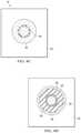
- FIG. 1shows a schematic of an annular RF shunt capacitor.
- FIG. 2shows a schematic of an annular RF shunt capacitor with dimensional information between the adjacent annular element and the via.
- FIG. 3shows a schematic of a cross section for annular RF shunt capacitor.
- FIGS. 4A to 4Fshow a step-by-step method of making the device of the present invention.
- FIGS. 4A and 4Bshow cross-sectional side views of two of the steps of the method.
- FIGS. 4C to 4Fshow the remained of the steps for making the annular capacitor RF, microwave and millimeter (MM) wave systems of the present invention.
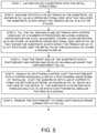
- FIG. 5shows a process flow to create a planarized surface in a substrate with dissimilar materials to eliminate vertical transitions from a substrate to an added material.
- the present inventionincludes a method for creating a substrate, an annular capacitor structure where the adjacent edge of the capacitive structure less than 250 ⁇ m of the via or imbedded metal structure in the substrate eliminates or minimizes the inductance associated with the metal line.
- FIG. 1shows an example of the device 10 , that includes ports 12 and 14 that connect to a top metal 16 , which can be a copper layer that is connected to, or shunted, to a through-via hole 18 .
- the design of the present inventionreduces the variability from the capacitor build.
- a top insulator 20is positioned between the top metal 16 and the via 18 , and a second metal layer 22 is deposited on the insulator 20 .
- the structureis formed in a substrate 24 .
- FIG. 2shows an internal view of the device 10 , that shows the gap 26 , between the through-hole via 18 and the first metal layer 16 .
- Ports 12 and 14 that connect to a top metal 16which can be a copper layer that connected to, or shunted, to a through-via hole 18 .
- FIG. 3is a cross-section side view of the device 10 . Ports 12 and 14 are shown in this configuration as being on opposite sides of the through-hole via 18 , which is isolated from the top metal layer 16 and the second top metal layer 22 , by insulator 20 . A bottom metal ground plane 28 is depicted connected to through-hole via 18 .
- FIGS. 4A to 4F and 5show a step-by-step method of making the device 10 of the present invention.
- the process flow to create a planarized surface in a substrate with dissimilar materials to eliminate vertical transitions from a substrate to an added materialis as follows:
- Step 1Lap and polish a substrate with the metal structures.
- Step 2.Machine or etch a via or trench in the substrate, as shown in FIG. 4A as a cross- sectional side view that includes the substrate 24 into which the trench or via 18 is cut or etched.
- Step 3.Fill the via, ground plane or trench with copper using any of a number of processes including chemical vapor deposition (CVD), silkscreen, atomic layer deposition (ALD) or other, as shown in cross-sectional side view in FIG. 4B that shows the substrate 24 into which the trench or via 18 is cut or etched, and the metal filled through-hole via 18 and a ground plane 28.
- CVDchemical vapor deposition
- ALDatomic layer deposition
- FIG. 4Bshows the substrate 24 into which the trench or via 18 is cut or etched, and the metal filled through-hole via 18 and a ground plane 28.
- One exampleis to selectively deposit tantalum on the sidewalls of the via or trench structures and then deposit copper organometallic by a silkscreen deposit
- the filled substrateis then heated in argon to drive off/decompose the organic material and densify the copper.
- the adhesion layeris a few hundred angstroms of tantalum.
- the adhesion layermay be removed over the metal.
- the thickness of the metal/non substrate materialneeds to be between two times and ten times the transition step.
- the thickness of the deposited materialcan be measured in real time using a variety of techniques including, e.g., a crystal oscillator during a vacuum deposition processes, where one side of the via is connected to a ground plane.
- Step 4.Coat the front side of the substrate with a photoresist and expose and develop an annular shape that circumscribes the via.
- Step 8Coat the front side of the substrate with a photoresist and expose and develop an annular shape that circumscribes the via, where the inner radii is between 2 ⁇ m and 300 ⁇ m from the outer edge of the metal filled via and external radii of the pattern is between 10 ⁇ m and 500 ⁇ m respectively.
- Step 8Using ALD or other deposition, deposit between 0.1 ⁇ m and 10 ⁇ m of a dielectric material, where the dielectric material has a dielectric constant between 2 and 2,000, as shown in FIG. 4D, which is a top view of the device 10.
- the substrate 24is shown in which a gap 32 is depicted between the through-hole via 18 and the second metal layer 22.
- Step 9Remove the photoresist to form a dielectric region that is at least 1 ⁇ m larger than the bottom electrode.
- Step 10.Coat the front side of the substrate with a photoresist and expose and develop an annular shape that is at least 2 ⁇ m greater than the dielectric layer and where one side transitions to other active or passive devices in the circuit.
- Step 11.Using a DC sputtering system, coat the photoresist with a copper adhesion layer is a few hundred angstroms of tantalum. Coat the substrate with 2 ⁇ m of copper to form the top electrode.
- Step 12.Remove the photoresist to form a top electrode for the capacitor structure, which is depicted in FIG.
- FIG. 4Ewhich shows the device 10, that now includes top metal layer 22, disposed on the insulator 20, and includes the gap 26, the bottom metal layer 16, the through-hole via 18, and the first metal layer 16.
- Step 13Coat the front side of the substrate with a photoresist and expose and develop a connecting metal line to both sides of the bottom metal of the annular structure.
- Step 14Using a DC sputtering system, coat the photoresist with a copper adhesion layer is a few hundred angstroms of tantalum. Coat the substrate with 2 ⁇ m of copper to form the top electrode.
- FIG. 4Fshows the device 10, which now includes all the layers and ports 12 and 14.
- the words “comprising”(and any form of comprising, such as “comprise” and “comprises”), “having” (and any form of having, such as “have” and “has”), “including” (and any form of including, such as “includes” and “include”) or “containing” (and any form of containing, such as “contains” and “contain”) are inclusive or open-ended and do not exclude additional, unrecited elements or method steps.
- “comprising”may be replaced with “consisting essentially of” or “consisting of”.
- the phrase “consisting essentially of”requires the specified integer(s) or steps as well as those that do not materially affect the character or function of the claimed invention.
- the term “consisting”is used to indicate the presence of the recited integer (e.g., a feature, an element, a characteristic, a property, a method/process step or a limitation) or group of integers (e.g., feature(s), element(s), characteristic(s), property(ies), method/process steps or limitation(s)) only.
- A, B, C, or combinations thereofrefers to all permutations and combinations of the listed items preceding the term.
- “A, B, C, or combinations thereof”is intended to include at least one of: A, B, C, AB, AC, BC, or ABC, and if order is important in a particular context, also BA, CA, CB, CBA, BCA, ACB, BAC, or CAB.
- expressly includedare combinations that contain repeats of one or more item or term, such as BB, AAA, AB, BBC, AAABCCCC, CBBAAA, CABABB, and so forth.
- BBBB
- AAAAAA
- ABBBC
- AAABCCCCCCCBBAAA
- CABABBCABABB
- words of approximationsuch as, without limitation, “about”, “substantial” or “substantially” refers to a condition that when so modified is understood to not necessarily be absolute or perfect but would be considered close enough to those of ordinary skill in the art to warrant designating the condition as being present.
- the extent to which the description may varywill depend on how great a change can be instituted and still have one of ordinary skilled in the art recognize the modified feature as still having the required characteristics and capabilities of the unmodified feature.
- a numerical value herein that is modified by a word of approximationsuch as “about” may vary from the stated value by at least ⁇ 1, 2, 3, 4, 5, 6, 7, 10, 12 or 15%.
- compositions and/or methods disclosed and claimed hereincan be made and executed without undue experimentation in light of the present disclosure. While the compositions and methods of this invention have been described in terms of preferred embodiments, it will be apparent to those of skill in the art that variations may be applied to the compositions and/or methods and in the steps or in the sequence of steps of the method described herein without departing from the concept, spirit and scope of the invention. All such similar substitutes and modifications apparent to those skilled in the art are deemed to be within the spirit, scope and concept of the invention as defined by the appended claims.
Landscapes
- Engineering & Computer Science (AREA)
- Power Engineering (AREA)
- Microelectronics & Electronic Packaging (AREA)
- Manufacturing & Machinery (AREA)
- Condensed Matter Physics & Semiconductors (AREA)
- Computer Hardware Design (AREA)
- General Physics & Mathematics (AREA)
- Physics & Mathematics (AREA)
- Chemical & Material Sciences (AREA)
- Ceramic Engineering (AREA)
- Inorganic Chemistry (AREA)
- Semiconductor Integrated Circuits (AREA)
- Ceramic Capacitors (AREA)
- Fixed Capacitors And Capacitor Manufacturing Machines (AREA)
Abstract
Description
| sectional side view that includes the |
| Step 3. Fill the via, ground plane or trench with copper using any of a number of processes |
| including chemical vapor deposition (CVD), silkscreen, atomic layer deposition (ALD) or other, |
| as shown in cross-sectional side view in FIG. 4B that shows the |
| trench or via 18 is cut or etched, and the metal filled through-hole via 18 and a |
| One example is to selectively deposit tantalum on the sidewalls of the via or trench structures |
| and then deposit copper organometallic by a silkscreen deposit. The filled substrate is then |
| heated in argon to drive off/decompose the organic material and densify the copper. For the |
| copper deposited, the adhesion layer is a few hundred angstroms of tantalum. The adhesion |
| layer may be removed over the metal. The thickness of the metal/non substrate material needs to |
| be between two times and ten times the transition step. The thickness of the deposited material |
| can be measured in real time using a variety of techniques including, e.g., a crystal oscillator |
| during a vacuum deposition processes, where one side of the via is connected to a ground plane. |
| shape that circumscribes the via. |
| Step 5. Using a DC sputtering system, coat the photoresist with a copper adhesion layer of a few |
| hundred angstroms of tantalum. Coat the substrate with 2 μm of copper to form the bottom |
| electrode, as shown in FIG. 4C, which is a top-view of the |
| with through-hole via 18, on which a bottom metal |
| Step 7. Coat the front side of the substrate with a photoresist and expose and develop an annular |
| shape that circumscribes the via, where the inner radii is between 2 μm and 300 μm from the |
| outer edge of the metal filled via and external radii of the pattern is between 10 μm and 500 μm |
| respectively. |
| Step 8. Using ALD or other deposition, deposit between 0.1 μm and 10 μm of a dielectric |
| material, where the dielectric material has a dielectric constant between 2 and 2,000, as shown in |
| FIG. 4D, which is a top view of the |
| depicted between the through-hole via 18 and the |
| insulator 20 (also referred to as a dielectric material). |
| Step 9. Remove the photoresist to form a dielectric region that is at least 1 μm larger than the |
| bottom electrode. |
| annular shape that is at least 2 μm greater than the dielectric layer and where one side transitions |
| to other active or passive devices in the circuit. |
| Step 11. Using a DC sputtering system, coat the photoresist with a copper adhesion layer is a |
| few hundred angstroms of tantalum. Coat the substrate with 2 μm of copper to form the top |
| electrode. |
| depicted in FIG. 4E, which shows the |
| on the |
| and the |
| connecting metal line to both sides of the bottom metal of the annular structure. |
| few hundred angstroms of tantalum. Coat the substrate with 2 μm of copper to form the top |
| electrode. FIG. 4F shows the |
Claims (22)
Priority Applications (1)
| Application Number | Priority Date | Filing Date | Title |
|---|---|---|---|
| US17/259,887US11270843B2 (en) | 2018-12-28 | 2019-12-26 | Annular capacitor RF, microwave and MM wave systems |
Applications Claiming Priority (3)
| Application Number | Priority Date | Filing Date | Title |
|---|---|---|---|
| US201862786165P | 2018-12-28 | 2018-12-28 | |
| PCT/US2019/068590WO2020139955A1 (en) | 2018-12-28 | 2019-12-26 | Annular capacitor rf, microwave and mm wave systems |
| US17/259,887US11270843B2 (en) | 2018-12-28 | 2019-12-26 | Annular capacitor RF, microwave and MM wave systems |
Publications (2)
| Publication Number | Publication Date |
|---|---|
| US20210225591A1 US20210225591A1 (en) | 2021-07-22 |
| US11270843B2true US11270843B2 (en) | 2022-03-08 |
Family
ID=71126397
Family Applications (1)
| Application Number | Title | Priority Date | Filing Date |
|---|---|---|---|
| US17/259,887ActiveUS11270843B2 (en) | 2018-12-28 | 2019-12-26 | Annular capacitor RF, microwave and MM wave systems |
Country Status (7)
| Country | Link |
|---|---|
| US (1) | US11270843B2 (en) |
| EP (1) | EP3903339A4 (en) |
| JP (1) | JP7257707B2 (en) |
| KR (1) | KR102392858B1 (en) |
| AU (1) | AU2019416327B2 (en) |
| CA (1) | CA3107812C (en) |
| WO (1) | WO2020139955A1 (en) |
Cited By (2)
| Publication number | Priority date | Publication date | Assignee | Title |
|---|---|---|---|---|
| US11908617B2 (en) | 2020-04-17 | 2024-02-20 | 3D Glass Solutions, Inc. | Broadband induction |
| US12431627B2 (en) | 2018-07-13 | 2025-09-30 | Knowles Cazenovia, Inc. | Millimeter wave filter array |
Families Citing this family (4)
| Publication number | Priority date | Publication date | Assignee | Title |
|---|---|---|---|---|
| US11139582B2 (en) | 2018-09-17 | 2021-10-05 | 3D Glass Solutions, Inc. | High efficiency compact slotted antenna with a ground plane |
| AU2019416327B2 (en) | 2018-12-28 | 2021-12-09 | 3D Glass Solutions, Inc. | Annular capacitor RF, microwave and MM wave systems |
| AU2019416325A1 (en) | 2018-12-28 | 2021-02-04 | 3D Glass Solutions, Inc. | Heterogenous integration for RF, microwave and mm wave systems in photoactive glass substrates |
| WO2022265783A1 (en)* | 2021-06-15 | 2022-12-22 | 3D Glass Solutions, Inc. | Radio frequency (rf) integrated power-conditioning capacitor |
Citations (241)
| Publication number | Priority date | Publication date | Assignee | Title |
|---|---|---|---|---|
| US2515941A (en) | 1946-09-09 | 1950-07-18 | Corning Glass Works | Photosensitive opal glass |
| US2515940A (en) | 1946-09-09 | 1950-07-18 | Corning Glass Works | Photosensitive opal glass |
| US2628160A (en) | 1951-08-30 | 1953-02-10 | Corning Glass Works | Sculpturing glass |
| US2684911A (en) | 1951-08-30 | 1954-07-27 | Corning Glass Works | Photosensitively opacifiable glass |
| US2971853A (en) | 1953-03-05 | 1961-02-14 | Corning Glass Works | Ceramic body and method of making it |
| US3281264A (en) | 1963-01-31 | 1966-10-25 | Coast Metals Inc | Method of gold-plating aluminum |
| US3904991A (en) | 1973-02-12 | 1975-09-09 | Tokyo Shibaura Electric Co | Stripline directional coupler having bent coupling arms |
| US3985531A (en) | 1975-03-19 | 1976-10-12 | Corning Glass Works | Spontaneously-formed fluormica glass-ceramics |
| US3993401A (en) | 1975-02-10 | 1976-11-23 | Minnesota Mining And Manufacturing Company | Retroreflective material including geometric fresnel zone plates |
| US4029605A (en) | 1975-12-08 | 1977-06-14 | Hercules Incorporated | Metallizing compositions |
| US4131516A (en) | 1977-07-21 | 1978-12-26 | International Business Machines Corporation | Method of making metal filled via holes in ceramic circuit boards |
| JPS5615587A (en) | 1979-07-17 | 1981-02-14 | Matsushita Electric Industrial Co Ltd | Sheathed heater with safety element |
| US4413061A (en) | 1978-02-06 | 1983-11-01 | International Business Machines Corporation | Glass-ceramic structures and sintered multilayer substrates thereof with circuit patterns of gold, silver or copper |
| US4444616A (en) | 1981-06-02 | 1984-04-24 | Hoya Corporation | Method for exposure of chemically machinable light-sensitive glass |
| US4514053A (en) | 1983-08-04 | 1985-04-30 | Corning Glass Works | Integral photosensitive optical device and method |
| US4537612A (en) | 1982-04-01 | 1985-08-27 | Corning Glass Works | Colored photochromic glasses and method |
| JPS61149905A (en) | 1984-12-25 | 1986-07-08 | Fujitsu Ltd | Optical multiplexer and demultiplexer |
| JPS61231529A (en) | 1985-04-08 | 1986-10-15 | Agency Of Ind Science & Technol | Optical control type optical switch device |
| US4647940A (en) | 1982-09-27 | 1987-03-03 | Rogers Corporation | Parallel plate waveguide antenna |
| JPS62202840A (en) | 1986-03-03 | 1987-09-07 | Toshiba Corp | Working of photosensitive glass |
| US4692015A (en) | 1986-03-14 | 1987-09-08 | Xerox Corporation | Short focal lens array with multi-magnification properties |
| JPS63128699A (en) | 1986-11-19 | 1988-06-01 | 株式会社日立製作所 | Light-sensitive glass-ceramic multilayer interconnection board |
| US4788165A (en) | 1987-10-07 | 1988-11-29 | Corning Glass Works | Copper-exuding, boroaluminosilicate glasses |
| EP0311274A2 (en) | 1987-10-07 | 1989-04-12 | Corning Glass Works | Thermal writing on glass or glass-ceramic substrates and copper-exuding glasses |
| US4942076A (en) | 1988-11-03 | 1990-07-17 | Micro Substrates, Inc. | Ceramic substrate with metal filled via holes for hybrid microcircuits and method of making the same |
| JPH0393683A (en) | 1989-09-01 | 1991-04-18 | Fujitsu Ltd | Copper paste and metallization method using the same |
| US5078771A (en) | 1989-02-07 | 1992-01-07 | Canyon Materials, Inc. | Method of making high energy beam sensitive glasses |
| US5147740A (en) | 1990-08-09 | 1992-09-15 | Rockwell International Corporation | Structure and process for fabricating conductive patterns having sub-half micron dimensions |
| EP0507719A1 (en) | 1991-04-04 | 1992-10-07 | International Business Machines Corporation | Improved glass-ceramic to copper adhesion |
| US5212120A (en) | 1991-06-10 | 1993-05-18 | Corning Incorporated | Photosensitive glass |
| JPH05139787A (en) | 1991-11-19 | 1993-06-08 | Seikosha Co Ltd | Working method for photosensitive glass |
| US5352996A (en) | 1992-01-30 | 1994-10-04 | Leader Electronics Corp. | Interdigital bandpass filter |
| US5371466A (en) | 1992-07-29 | 1994-12-06 | The Regents Of The University Of California | MRI RF ground breaker assembly |
| US5374291A (en) | 1991-12-10 | 1994-12-20 | Director-General Of Agency Of Industrial Science And Technology | Method of processing photosensitive glass |
| US5395498A (en) | 1991-11-06 | 1995-03-07 | Gombinsky; Moshe | Method for separating biological macromolecules and means therfor |
| US5409741A (en) | 1991-04-12 | 1995-04-25 | Laude; Lucien D. | Method for metallizing surfaces by means of metal powders |
| JPH0826767A (en) | 1994-07-13 | 1996-01-30 | Nippon Glass Kk | Soda lime-silica photosensitive glass and its production |
| JPH08179155A (en) | 1994-12-26 | 1996-07-12 | Ricoh Co Ltd | Method for coupling lens and optical fiber and method for producing lens substrate |
| JPH107435A (en) | 1996-06-26 | 1998-01-13 | Ngk Spark Plug Co Ltd | Glass ceramic wiring substrate and its production |
| US5733370A (en) | 1996-01-16 | 1998-03-31 | Seagate Technology, Inc. | Method of manufacturing a bicrystal cluster magnetic recording medium |
| US5779521A (en) | 1995-03-03 | 1998-07-14 | Sony Corporation | Method and apparatus for chemical/mechanical polishing |
| JPH10199728A (en) | 1997-01-07 | 1998-07-31 | Murata Mfg Co Ltd | Thin-film coil component and method of manufacturing the same |
| US5850623A (en) | 1997-03-14 | 1998-12-15 | Eastman Chemical Company | Method for standardizing raman spectrometers to obtain stable and transferable calibrations |
| US5902715A (en) | 1992-11-09 | 1999-05-11 | Fujitsu Limited | Method of forming a mirror in a waveguide |
| US5919607A (en) | 1995-10-26 | 1999-07-06 | Brown University Research Foundation | Photo-encoded selective etching for glass based microtechnology applications |
| EP0685857B1 (en) | 1994-06-03 | 1999-09-08 | Mitel Semiconductor Limited | Inductor chip device |
| EP0949648A1 (en) | 1996-09-26 | 1999-10-13 | Asahi Glass Company Ltd. | Plasma display protective plate and its manufacturing method |
| US5998224A (en) | 1997-05-16 | 1999-12-07 | Abbott Laboratories | Magnetically assisted binding assays utilizing a magnetically responsive reagent |
| JPH11344648A (en) | 1998-05-07 | 1999-12-14 | Trw Inc | Fiber/waveguide-mirror-lens alignment device |
| US6066448A (en) | 1995-03-10 | 2000-05-23 | Meso Sclae Technologies, Llc. | Multi-array, multi-specific electrochemiluminescence testing |
| US6094336A (en) | 1997-04-25 | 2000-07-25 | U.S. Philips Corporation | Enveloped multilayer capacitor |
| JP2000228615A (en) | 1999-02-05 | 2000-08-15 | Tokin Corp | Lc bandpass filter |
| US6136210A (en) | 1998-11-02 | 2000-10-24 | Xerox Corporation | Photoetching of acoustic lenses for acoustic ink printing |
| US6171886B1 (en) | 1998-06-30 | 2001-01-09 | Eastman Kodak Company | Method of making integrated hybrid silicon-based micro-actuator devices |
| JP2001033664A (en) | 1999-07-21 | 2001-02-09 | Hitachi Cable Ltd | Optical fiber block |
| US6258497B1 (en) | 1992-07-29 | 2001-07-10 | International Business Machines Corporation | Precise endpoint detection for etching processes |
| JP2001206735A (en) | 2000-01-25 | 2001-07-31 | Central Glass Co Ltd | Plating method |
| US6287965B1 (en) | 1997-07-28 | 2001-09-11 | Samsung Electronics Co, Ltd. | Method of forming metal layer using atomic layer deposition and semiconductor device having the metal layer as barrier metal layer or upper or lower electrode of capacitor |
| US6329702B1 (en) | 2000-07-06 | 2001-12-11 | Tyco Electronics Corporation | High frequency carrier |
| US20010051584A1 (en) | 2000-04-26 | 2001-12-13 | Matsushita Electric Industrial Co., Ltd. | Dielectric ceramic composition and method for producing the same, and device for communication apparatus using the same |
| US20020015546A1 (en) | 2000-07-31 | 2002-02-07 | Bhagavatula Venkata A. | Bulk internal bragg gratings and optical devices |
| US6373369B2 (en) | 1999-07-26 | 2002-04-16 | Taiwan Semiconductor Manufacturing Company | High efficiency thin film inductor |
| US6383566B1 (en) | 1999-06-30 | 2002-05-07 | Saint-Gobain Vitrage | Process for depositing a tungsten-based and/or molybdenum-based layer on a rigid substrate, and substrate thus coated |
| US20020086246A1 (en) | 2000-12-30 | 2002-07-04 | Lg Electronics Inc. | Method of fabricating barrier ribs in plasma display panel |
| US20020100608A1 (en) | 1999-05-27 | 2002-08-01 | Hoya Corporation | Multilayer printed wiring board and a process of producing same |
| US6485690B1 (en) | 1999-05-27 | 2002-11-26 | Orchid Biosciences, Inc. | Multiple fluid sample processor and system |
| US6495411B1 (en) | 2000-07-13 | 2002-12-17 | Promos Technology Inc. | Technique to improve deep trench capacitance by increasing surface thereof |
| US6511793B1 (en) | 1999-03-24 | 2003-01-28 | Lg Electronics Inc. | Method of manufacturing microstructure using photosensitive glass substrate |
| US6514375B2 (en) | 1997-12-15 | 2003-02-04 | Ricoh Company, Ltd. | Dry etching endpoint detection system |
| US20030025227A1 (en) | 2001-08-02 | 2003-02-06 | Zograph, Llc | Reproduction of relief patterns |
| US6562523B1 (en) | 1996-10-31 | 2003-05-13 | Canyon Materials, Inc. | Direct write all-glass photomask blanks |
| US20030124716A1 (en) | 2000-10-10 | 2003-07-03 | Biotrove, Inc., A Delaware Corporation | Apparatus for assay, synthesis and storage, and methods of manufacture, use, and manipulation thereof |
| US20030135201A1 (en) | 2001-09-28 | 2003-07-17 | Gonnelli Robert R. | Microneedle with membrane |
| US20030156819A1 (en) | 2002-02-15 | 2003-08-21 | Mark Pruss | Optical waveguide |
| US20030174944A1 (en) | 2002-03-14 | 2003-09-18 | Corning Incorporated | Fiber array and methods for fabricating the fiber array |
| US20030228682A1 (en) | 2002-04-30 | 2003-12-11 | University Of Maryland, Baltimore | Fluorescence sensing |
| US20030231830A1 (en) | 2002-05-14 | 2003-12-18 | Naoko Hikichi | Optical module |
| US6678453B2 (en) | 1999-11-04 | 2004-01-13 | Corning Incorporated | High aspect ratio patterning of glass film |
| US20040008391A1 (en) | 1999-09-16 | 2004-01-15 | Bowley Christopher C. | Holographically-formed polymer dispersed liquid crystals with multiple gratings |
| US6686824B1 (en) | 1998-05-29 | 2004-02-03 | Nissha Printing Co., Ltd. | Toroidal printed coil |
| US20040020690A1 (en) | 1998-03-20 | 2004-02-05 | Parker John Leroy | Via connector and method of making same |
| US6771860B2 (en) | 2001-06-29 | 2004-08-03 | Xanoptix, Inc. | Module mounted aligning optical connector |
| US20040155748A1 (en) | 2003-02-02 | 2004-08-12 | Dietrich Steingroever | Transformer for producing high electrical currents |
| US6783920B2 (en) | 2003-01-15 | 2004-08-31 | The Aerospace Corporation | Photosensitive glass variable laser exposure patterning method |
| US20040171076A1 (en) | 2001-12-20 | 2004-09-02 | Dejneka Matthew J. | Detectable micro to nano sized structures, methods of manufacture and use |
| US20040184705A1 (en) | 2003-01-08 | 2004-09-23 | Mikihiro Shimada | Optical waveguide component and method of manufacturing the same |
| US20040198582A1 (en) | 2003-04-01 | 2004-10-07 | Borrelli Nicholas F. | Optical elements and methods of making optical elements |
| US20040227596A1 (en) | 2003-02-11 | 2004-11-18 | Nguyen John A. | Ultra broadband inductor assembly |
| US6824974B2 (en) | 2001-06-11 | 2004-11-30 | Genorx, Inc. | Electronic detection of biological molecules using thin layers |
| CN1562831A (en) | 2004-04-16 | 2005-01-12 | 武汉理工大学 | Method for preparing microcrystalline glass/glass carrier material having nano holes in high density |
| US6843902B1 (en) | 2001-07-20 | 2005-01-18 | The Regents Of The University Of California | Methods for fabricating metal nanowires |
| US6875544B1 (en) | 2002-10-03 | 2005-04-05 | Sandia Corporation | Method for the fabrication of three-dimensional microstructures by deep X-ray lithography |
| US20050089901A1 (en) | 2000-09-22 | 2005-04-28 | Porter Marc D. | Raman-active reagents and the use thereof |
| US20050105860A1 (en) | 2003-02-24 | 2005-05-19 | Ngk Spark Plug Co., Ltd. | Optical device mounted substrate assembly |
| US20050150683A1 (en) | 2004-01-12 | 2005-07-14 | Farnworth Warren M. | Methods of fabricating substrates and substrate precursor structures resulting therefrom |
| US20050170670A1 (en) | 2003-11-17 | 2005-08-04 | King William P. | Patterning of sacrificial materials |
| JP2005215644A (en) | 2004-02-02 | 2005-08-11 | Sharp Corp | Optical module and manufacturing method thereof |
| US6932933B2 (en) | 2001-03-30 | 2005-08-23 | The Aerospace Corporation | Ultraviolet method of embedding structures in photocerams |
| US20050212432A1 (en) | 2005-06-27 | 2005-09-29 | Osram Sylvania Inc. | Incandescent lamp that emits infrared light and a method of making the lamp |
| JP2005302987A (en) | 2004-04-12 | 2005-10-27 | Dainippon Printing Co Ltd | Passive element built-in wiring board and manufacturing method thereof |
| US20050277550A1 (en) | 2004-06-09 | 2005-12-15 | Ferro Corporation | Lead-free and cadmium-free conductive copper thick film pastes |
| US6977722B2 (en) | 2001-06-29 | 2005-12-20 | Meso Scale Technologies, Llc. | Assay plates, reader systems and methods for luminescence test measurements |
| DE102004059252A1 (en) | 2004-06-09 | 2006-01-19 | Schott Ag | Optically active structure application method for Fresnel lens manufacture, involves photographic structuring photosensitive resist layer, coating substrate with optically active layer and lifting-off resist layer |
| US7033821B2 (en) | 2000-11-08 | 2006-04-25 | Surface Logix, Inc. | Device for monitoring cell motility in real-time |
| US20060092079A1 (en) | 2004-10-01 | 2006-05-04 | De Rochemont L P | Ceramic antenna module and methods of manufacture thereof |
| US20060118965A1 (en) | 2004-12-02 | 2006-06-08 | Nec Electronics Corporation | Semiconductor device, semiconductor module employing thereof and method for manufacturing semiconductor device |
| JP2006179564A (en) | 2004-12-21 | 2006-07-06 | Nec Corp | Semiconductor connection substrate, method of manufacturing the same semiconductor apparatus, semiconductor device, and semiconductor substrate |
| US20060147344A1 (en) | 2004-09-30 | 2006-07-06 | The University Of Cincinnati | Fully packed capillary electrophoretic separation microchips with self-assembled silica colloidal particles in microchannels and their preparation methods |
| US20060158300A1 (en) | 2005-01-20 | 2006-07-20 | Avx Corporation | High Q planar inductors and IPD applications |
| US20060159916A1 (en) | 2003-05-05 | 2006-07-20 | Nanosys, Inc. | Nanofiber surfaces for use in enhanced surface area applications |
| EP1683571A1 (en) | 2005-01-20 | 2006-07-26 | Samsung Electronics Co., Ltd. | Patterning method, substrate for biomolecule immobilization using the patterning method, and biochip employing the substrate |
| US20060171033A1 (en) | 2004-12-31 | 2006-08-03 | Schott Ag | Method for producing an optical component, optical component produced according to the method and devices comprising such components |
| US20060177855A1 (en) | 2005-01-21 | 2006-08-10 | Utermohlen Joseph G | Nanoparticles for manipulation of biopolymers and methods of thereof |
| US20060193214A1 (en) | 2005-02-28 | 2006-08-31 | Takeshi Shimano | Optical head, optical information storage apparatus, and their fabrication method |
| US7132054B1 (en) | 2004-09-08 | 2006-11-07 | Sandia Corporation | Method to fabricate hollow microneedle arrays |
| US20060283948A1 (en) | 2005-06-20 | 2006-12-21 | Denso Corporation | Antenna coil, resonant antenna having antenna coil, and card type wireless device having resonant antenna |
| US7179638B2 (en) | 1999-07-30 | 2007-02-20 | Large Scale Biology Corporation | Microarrays and their manufacture by slicing |
| US20070120263A1 (en) | 2005-08-19 | 2007-05-31 | Zvonimir Gabric | Conductor track arrangement and associated production method |
| US20070121263A1 (en) | 2005-11-29 | 2007-05-31 | Jeng-Shu Liu | Timing controller chip |
| US20070155021A1 (en) | 2005-12-29 | 2007-07-05 | Intel Corporation | Modification of metal nanoparticles for improved analyte detection by surface enhanced Raman spectroscopy (SERS) |
| US20070158787A1 (en) | 2003-11-13 | 2007-07-12 | Rajen Chanchani | Heterogeneously integrated microsystem-on-a-chip |
| WO2007088058A2 (en) | 2006-02-02 | 2007-08-09 | Xsil Technology Limited | Support for wafer singulation |
| US7277151B2 (en) | 2001-10-15 | 2007-10-02 | Samsung Sdi Co., Ltd. | Flat panel display with photosensitive glass spacer |
| US20070248126A1 (en) | 2002-06-10 | 2007-10-25 | New Wave Research | Scribing sapphire substrates with a solid state uv laser |
| US20070267708A1 (en) | 2006-05-22 | 2007-11-22 | Cardiomems, Inc. | Methods and apparatus having an integrated circuit attached to fused silica |
| US20070272829A1 (en) | 2006-05-29 | 2007-11-29 | Atsuo Nakagawa | Solid-state imaging device and method for fabricating the same |
| US20070279837A1 (en) | 2004-03-18 | 2007-12-06 | Nanosys, Inc. | Nanofiber Surface Based Capacitors |
| US7306689B2 (en) | 1998-10-27 | 2007-12-11 | Sony Corporation | Optical waveguide and method for producing same |
| US20070296520A1 (en) | 2005-04-18 | 2007-12-27 | Murata Manufacturing Co., Ltd. | High-frequency module |
| US7326538B2 (en) | 2002-01-04 | 2008-02-05 | Becton Dickinson And Company | Binding proteins as biosensors |
| US20080136572A1 (en) | 2006-12-06 | 2008-06-12 | Farrokh Ayazi | Micro-electromechanical switched tunable inductor |
| US20080174976A1 (en) | 2001-07-12 | 2008-07-24 | Hitachi, Ltd. | Electronic Circuit Component |
| US20080182079A1 (en) | 2006-06-28 | 2008-07-31 | Northwestern University | Etching and hole arrays |
| US7407768B2 (en) | 2002-09-11 | 2008-08-05 | Synamem Corporation | Membrane-based assays |
| US7410763B2 (en) | 2005-09-01 | 2008-08-12 | Intel Corporation | Multiplex data collection and analysis in bioanalyte detection |
| US20080223603A1 (en) | 2007-03-12 | 2008-09-18 | Samsung Electro-Mechanics Co., Ltd. | Capacitor embedded printed circuit board |
| US20080226228A1 (en) | 2007-03-15 | 2008-09-18 | Hitachi Cable, Ltd. | Optical system connection structure, optical component, and optical communication module |
| WO2008119080A1 (en) | 2007-03-28 | 2008-10-02 | Life Bioscience Inc. | Compositions and methods to fabricate a photoactive substrate suitable for shaped glass structures |
| JP2008252797A (en) | 2007-03-30 | 2008-10-16 | Tdk Corp | Dielectric resonator, dielectric filter, and characteristic adjustment method thereof |
| US7439128B2 (en) | 2003-04-07 | 2008-10-21 | International Business Machines Corporation | Method of creating deep trench capacitor using a P+ metal electrode |
| US20080291442A1 (en) | 2005-06-13 | 2008-11-27 | Solaris Nanosciences, Inc. | Chemical and biological sensing using metallic particles in amplifying and absorbing media |
| US20080305268A1 (en) | 2007-06-05 | 2008-12-11 | Air Products And Chemicals, Inc. | Low Temperature Thermal Conductive Inks |
| WO2008154931A1 (en) | 2007-06-18 | 2008-12-24 | Danmarks Tekniske Universitet (Technical University Of Denmark) | Adsorbent beads suitable for use in separation of biological molecules |
| US20080316678A1 (en) | 2006-07-14 | 2008-12-25 | Ehrenberg Scott G | Nanoparticle ultracapacitor |
| US7470518B2 (en) | 2002-02-12 | 2008-12-30 | Cellectricon Ab | Systems and method for rapidly changing the solution environment around sensors |
| US20090029185A1 (en) | 2007-07-27 | 2009-01-29 | Cheng-Chang Lee | Magnetic device and manufacturing method thereof |
| US7497554B2 (en) | 2004-07-22 | 2009-03-03 | Konica Minolta Holdings, Inc. | Ink jet print head |
| WO2009029733A2 (en) | 2007-08-28 | 2009-03-05 | Life Biosciences, Inc. | Method of providing a pattern of biological-binding areas for biological testing |
| WO2009062011A1 (en) | 2007-11-07 | 2009-05-14 | Masachusetts Institute Of Technology | Method of forming a locally periodic 3d structure with larger-scale variation in periodic properties and applications thereof |
| US20090130736A1 (en) | 2003-02-06 | 2009-05-21 | Becton, Dickinson And Company | Pretreatment method for extraction of nucleic acid from biological samples and kits therefor |
| US20090170032A1 (en) | 2007-12-28 | 2009-07-02 | Fujitsu Media Devices Limited | Method of manufacturing electronic device |
| US20090182720A1 (en) | 2008-01-15 | 2009-07-16 | Cain Michael W | Maintained Symbol Table Only Index |
| US20090243783A1 (en) | 2006-08-28 | 2009-10-01 | Avago Technologies Ecbu (Singapore) Pte. Ltd. | Minimizing Electromagnetic Interference in Coil Transducers |
| WO2009126649A2 (en) | 2008-04-07 | 2009-10-15 | Life Bioscience, Inc. | Method of providing particles having biological-binding areas for biological applications |
| US20100022416A1 (en) | 2008-07-25 | 2010-01-28 | Life Bioscience, Inc. | Assay plates, methods and systems having one or more etched features |
| KR100941691B1 (en) | 2009-04-10 | 2010-02-12 | (주)제이스 | Photosensitve glass wafer and method for manufacturing potosensitve glass wafer and semiconductor probe chip |
| US20100059265A1 (en) | 2008-09-11 | 2010-03-11 | Myung-Soo Kim | Contact of semiconductor device and manufacturing method thereof |
| US20100237462A1 (en) | 2009-03-18 | 2010-09-23 | Benjamin Beker | Package Level Tuning Techniques for Propagation Channels of High-Speed Signals |
| US20110003422A1 (en) | 2009-07-02 | 2011-01-06 | Advanced Microfab, LLC | Method of forming monolithic cmos-mems hybrid integrated, packaged structures |
| US20110045284A1 (en) | 2008-03-12 | 2011-02-24 | Dai Nippon Printing Co., Ltd. | Decorative sheet for three-dimensional work |
| US20110065662A1 (en) | 2009-07-24 | 2011-03-17 | Amazentis Sa | Compounds, Compositions, and Methods for Protecting Brain Health in Neurodegenerative Disorders |
| US20110108525A1 (en) | 2009-11-11 | 2011-05-12 | Industrial Technology Research Institute | Method and system for manufacturing microstructure in photosensitive glass substrate |
| US7948342B2 (en) | 2008-07-24 | 2011-05-24 | Cutt-A-Watt Enterprises, Llc | Electromotive rectification system |
| US20110170273A1 (en) | 2010-01-13 | 2011-07-14 | The Aerospace Corporation | Photostructured Magnetic Devices and Methods for Making Same |
| US20110195360A1 (en) | 2010-02-10 | 2011-08-11 | Life Bioscience, Inc. | Methods to fabricate a photoactive substrate suitable for microfabrication |
| US20110217657A1 (en) | 2010-02-10 | 2011-09-08 | Life Bioscience, Inc. | Methods to fabricate a photoactive substrate suitable for microfabrication |
| WO2011109648A1 (en) | 2010-03-03 | 2011-09-09 | Georgia Tech Research Corporation | Through-package-via (tpv) structures on inorganic interposer and methods for fabricating same |
| US20110284725A1 (en) | 2008-03-04 | 2011-11-24 | The Regents Of The Univeristy Of California | Microlens arrays for enhanced light concentration |
| US20110304999A1 (en) | 2010-06-10 | 2011-12-15 | Taiwan Semiconductor Manufacturing Company, Ltd. | Interposer-on-Glass Package Structures |
| US20120080612A1 (en) | 2009-04-03 | 2012-04-05 | Research Triangle Institute | Cantilever-based mems optical scanning apparatus, system and method |
| JP2012079960A (en) | 2010-10-04 | 2012-04-19 | Denso Corp | Capacitor structure and method for manufacturing the same |
| WO2012078213A1 (en) | 2010-12-09 | 2012-06-14 | Tessera Inc | High density three-dimensional integrated capacitors |
| US20120161330A1 (en) | 2010-12-22 | 2012-06-28 | Intel Corporation | Device packaging with substrates having embedded lines and metal defined pads |
| KR101167691B1 (en) | 2011-08-09 | 2012-07-20 | 주식회사 비티엔아이티솔루션스 | Multilayer capacitor having photosensitive glass, fabrication method thereof, and the use the same |
| JP2013062473A (en) | 2011-09-15 | 2013-04-04 | Toppan Printing Co Ltd | Wiring board and manufacturing method therefor |
| US20130119401A1 (en) | 2010-06-18 | 2013-05-16 | Soraa, Inc. | Large area nitride crystal and method for making it |
| US20130183805A1 (en) | 2010-09-14 | 2013-07-18 | International Business Machines Corporation | High capacitance trench capacitor |
| US20130209026A1 (en) | 2012-02-10 | 2013-08-15 | International Business Machines Corporation | Through-substrate optical coupling to photonics chips |
| US20130233202A1 (en) | 2010-12-03 | 2013-09-12 | Ei Du Pont De Nemours And Company | Inks and processes for preparing copper indium gallium sulfide/selenide coatings and films |
| JP2013217989A (en) | 2012-04-04 | 2013-10-24 | Hitachi Chemical Co Ltd | Optical fiber connector |
| US20130278568A1 (en) | 2012-04-24 | 2013-10-24 | Qualcomm Mems Technologies, Inc. | Metal-insulator-metal capacitors on glass substrates |
| US20130308906A1 (en) | 2012-05-21 | 2013-11-21 | LaXense, Inc. | System and method for dense coupling between optical devices and an optical fiber array |
| US20130337604A1 (en) | 2012-06-19 | 2013-12-19 | E I Du Pont De Nemours And Company | Method of manufacturing thick-film electrode |
| US20140002906A1 (en) | 2011-03-17 | 2014-01-02 | Enplas Corporation | Lens array |
| US20140035892A1 (en) | 2012-08-03 | 2014-02-06 | Qualcomm Mems Technologies, Inc. | Incorporation of passives and fine pitch through via for package on package |
| US20140035935A1 (en) | 2012-08-03 | 2014-02-06 | Qualcomm Mems Technologies, Inc. | Passives via bar |
| US20140035540A1 (en) | 2012-02-08 | 2014-02-06 | Dais Analytic Corporation | Energy storage device and methods |
| US20140070380A1 (en) | 2012-09-11 | 2014-03-13 | Chia-Pin Chiu | Bridge interconnect with air gap in package assembly |
| WO2014043267A1 (en) | 2012-09-12 | 2014-03-20 | Life Bioscience, Inc. | Methods of fabricating photoactive substrates suitable for electromagnetic transmission and filtering applications |
| US20140104284A1 (en) | 2012-10-16 | 2014-04-17 | Qualcomm Mems Technologies, Inc. | Through substrate via inductors |
| WO2014062226A1 (en) | 2012-10-19 | 2014-04-24 | Rutgers, The State University Of New Jersey | In situ exfoliation method to fabricate a graphene-reinforced polymer matrix composite |
| US20140145326A1 (en) | 2012-11-29 | 2014-05-29 | United Microelectronics Corp. | Substrate with integrated passive devices and method of manufacturing the same |
| US20140144681A1 (en) | 2012-11-27 | 2014-05-29 | Qualcomm Mems Technologies, Inc. | Adhesive metal nitride on glass and related methods |
| US20140169746A1 (en) | 2012-12-14 | 2014-06-19 | Hon Hai Precision Industry Co., Ltd. | Optical connector with sloped surface |
| US20140203891A1 (en) | 2012-01-16 | 2014-07-24 | Murata Manufacturing Co., Ltd. | Rf signal blocking device |
| US20140247269A1 (en) | 2013-03-04 | 2014-09-04 | Qualcomm Mems Technologies, Inc. | High density, low loss 3-d through-glass inductor with magnetic core |
| US20140272688A1 (en) | 2013-03-15 | 2014-09-18 | Photronics, Inc. | Grayscale lithography of photo definable glass |
| US20140367695A1 (en) | 2013-06-18 | 2014-12-18 | Stephen P. Barlow | Trench high electron mobility transistor device |
| JP2014241365A (en) | 2013-06-12 | 2014-12-25 | 株式会社デンソー | Penetration type capacitor |
| JP2015028651A (en) | 2006-12-22 | 2015-02-12 | シスコ テクノロジー,インコーポレイテッド | Dual-lensed unitary optical receiver assembly |
| US20150048901A1 (en) | 2013-08-19 | 2015-02-19 | Harris Corporation | Microelectromechanical systems comprising differential inductors and methods for making the same |
| WO2015108648A1 (en) | 2014-01-14 | 2015-07-23 | Qualcomm Incorporated | A stacked conductive interconnect inductor |
| US20150210074A1 (en) | 2012-08-16 | 2015-07-30 | Chien-Hua Chen | Diagonal openings in photodefinable glass |
| WO2015112903A1 (en) | 2014-01-24 | 2015-07-30 | 3D Glass Solutions, Inc | Methods of fabricating photoactive substrates for micro-lenses and arrays |
| US20150263429A1 (en) | 2011-08-31 | 2015-09-17 | Mehrnoosh Vahidpour | Micromachined millimeter-wave frequency scanning array |
| WO2015171597A1 (en) | 2014-05-05 | 2015-11-12 | 3D Glass Solutions, Inc. | 2d and 3d inductors antenna and transformers fabricating photoactive substrates |
| US20160048079A1 (en) | 2014-08-12 | 2016-02-18 | Su-Young Lee | Method, photolithography method, and method of manufacturing a semiconductor device using a pellicle film |
| US20160181211A1 (en) | 2013-09-27 | 2016-06-23 | Intel Corporation | Die package with superposer substrate for passive components |
| US20160185653A1 (en) | 2013-09-04 | 2016-06-30 | Hoya Corporation | Silicate ceramics, plate-like substrate, and method of producing plate-like substrate |
| US9385083B1 (en) | 2015-05-22 | 2016-07-05 | Hrl Laboratories, Llc | Wafer-level die to package and die to die interconnects suspended over integrated heat sinks |
| US20160254579A1 (en) | 2013-10-07 | 2016-09-01 | Koninklijke Philips N.V. | Precision batch production method for manufacturing ferrite rods |
| CN105938928A (en) | 2015-03-04 | 2016-09-14 | 天工方案公司 | Devices and methods related to multiple-pole ceramic resonator filters |
| US20160268665A1 (en) | 2003-03-04 | 2016-09-15 | Nuvotronics, Inc | Coaxial Waveguide Microstructures Having an Active Device and Methods of Formation Thereof |
| US20160265974A1 (en) | 2015-03-09 | 2016-09-15 | Corning Incorporated | Glass waveguide spectrophotometer |
| US9449753B2 (en) | 2013-08-30 | 2016-09-20 | Qualcomm Incorporated | Varying thickness inductor |
| US20160320568A1 (en) | 2013-12-19 | 2016-11-03 | 3M Innovative Properties Company | Multimode optical connector |
| US20160380614A1 (en) | 2015-06-26 | 2016-12-29 | Rf Micro Devices, Inc. | Saw resonator with resonant cavities |
| US20170077892A1 (en) | 2015-09-15 | 2017-03-16 | Karl L. Thorup | High isolation power combiner/splitter and coupler |
| US20170094794A1 (en) | 2015-09-30 | 2017-03-30 | 3D Glass Solutions, Inc | Photo-definable glass with integrated electronics and ground plane |
| US9635757B1 (en) | 2016-08-11 | 2017-04-25 | Unimicron Technology Corp. | Circuit board and manufacturing method thereof |
| US20170213762A1 (en) | 2016-01-21 | 2017-07-27 | Applied Materials, Inc. | Process and chemistry of plating of through silicon vias |
| WO2017132280A2 (en) | 2016-01-31 | 2017-08-03 | 3D Glass Solutions, Inc. | Multi-layer photo definable glass with integrated devices |
| WO2017147511A1 (en) | 2016-02-25 | 2017-08-31 | 3D Glass Solutions, Inc. | 3d capacitor and capacitor array fabricating photoactive substrates |
| US9755305B2 (en) | 2012-08-16 | 2017-09-05 | Ethertronics, Inc. | Active antenna adapted for impedance matching and band switching using a shared component |
| WO2017177171A1 (en) | 2016-04-08 | 2017-10-12 | 3D Glass Solutions, Inc. | Methods of fabricating photosensitive substrates suitable for optical coupler |
| US9819991B1 (en) | 2016-02-29 | 2017-11-14 | Amazon Technologies, Inc. | Adaptive impedance matching interface |
| WO2018200804A1 (en) | 2017-04-28 | 2018-11-01 | 3D Glass Solutions, Inc. | Rf circulator |
| US20180323485A1 (en) | 2017-05-02 | 2018-11-08 | Bae Systems Information And Electronic Systems Integration Inc. | Miniature ltcc coupled stripline resonator filters for digital receivers |
| JP2018200912A (en) | 2017-05-25 | 2018-12-20 | 凸版印刷株式会社 | Built-in capacitor glass circuit board and manufacturing method thereof |
| WO2019010045A1 (en) | 2017-07-07 | 2019-01-10 | 3D Glass Solutions, Inc. | 2d and 3d rf lumped element devices for rf system in a package photoactive glass substrates |
| US10201901B2 (en) | 2015-01-29 | 2019-02-12 | Canon Kabushiki Kaisha | Robot apparatus, method for controlling robot, program, and recording medium |
| WO2019118761A1 (en) | 2017-12-15 | 2019-06-20 | 3D Glass Solutions, Inc. | Coupled transmission line resonate rf filter |
| WO2019136024A1 (en) | 2018-01-04 | 2019-07-11 | 3D Glass Solutions, Inc. | Impedance matching conductive structure for high efficiency rf circuits |
| US20190280079A1 (en) | 2016-11-24 | 2019-09-12 | Murata Integrated Passive Solutions | Integrated electronic component suitable for broadband biasing |
| WO2019199470A1 (en) | 2018-04-10 | 2019-10-17 | 3D Glass Solutions, Inc. | Rf integrated power condition capacitor |
| WO2019231947A1 (en) | 2018-05-29 | 2019-12-05 | 3D Glass Solutions, Inc. | Low insertion loss rf transmission line |
| WO2020060824A1 (en) | 2018-09-17 | 2020-03-26 | 3D Glass Solutions, Inc. | High efficiency compact slotted antenna with a ground plane |
| CN210668058U (en) | 2019-12-09 | 2020-06-02 | 梅州市成就电子科技有限公司 | A Broadband Conical Inductor |
| WO2020139951A1 (en) | 2018-12-28 | 2020-07-02 | 3D Glass Solutions, Inc. | Heterogenous integration for rf, microwave and mm wave systems in photoactive glass substrates |
| WO2020139955A1 (en) | 2018-12-28 | 2020-07-02 | 3D Glass Solutions, Inc. | Annular capacitor rf, microwave and mm wave systems |
| US20200275558A1 (en) | 2017-12-11 | 2020-08-27 | Toppan Printing Co.,Ltd. | Glass wiring board, method for manufacturing the same, and semiconductor device |
Family Cites Families (6)
| Publication number | Priority date | Publication date | Assignee | Title |
|---|---|---|---|---|
| JPS58125907A (en)* | 1982-01-22 | 1983-07-27 | Nissan Motor Co Ltd | High frequency noise removal filter |
| JPS5939949U (en)* | 1982-09-08 | 1984-03-14 | アルプス電気株式会社 | High frequency circuit equipment |
| US6538538B2 (en) | 1999-02-25 | 2003-03-25 | Formfactor, Inc. | High frequency printed circuit board via |
| US7190594B2 (en) | 2004-05-14 | 2007-03-13 | Commscope Solutions Properties, Llc | Next high frequency improvement by using frequency dependent effective capacitance |
| JP5868574B2 (en)* | 2010-03-15 | 2016-02-24 | 富士通株式会社 | Semiconductor device and manufacturing method thereof |
| US9548350B2 (en)* | 2014-02-10 | 2017-01-17 | Qualcomm Incorporated | High quality factor capacitors and methods for fabricating high quality factor capacitors |
- 2019
- 2019-12-26AUAU2019416327Apatent/AU2019416327B2/ennot_activeExpired - Fee Related
- 2019-12-26USUS17/259,887patent/US11270843B2/enactiveActive
- 2019-12-26EPEP19905255.6Apatent/EP3903339A4/ennot_activeWithdrawn
- 2019-12-26JPJP2021503065Apatent/JP7257707B2/enactiveActive
- 2019-12-26KRKR1020217014441Apatent/KR102392858B1/enactiveActive
- 2019-12-26WOPCT/US2019/068590patent/WO2020139955A1/ennot_activeCeased
- 2019-12-26CACA3107812Apatent/CA3107812C/enactiveActive
Patent Citations (260)
| Publication number | Priority date | Publication date | Assignee | Title |
|---|---|---|---|---|
| US2515941A (en) | 1946-09-09 | 1950-07-18 | Corning Glass Works | Photosensitive opal glass |
| US2515940A (en) | 1946-09-09 | 1950-07-18 | Corning Glass Works | Photosensitive opal glass |
| US2628160A (en) | 1951-08-30 | 1953-02-10 | Corning Glass Works | Sculpturing glass |
| US2684911A (en) | 1951-08-30 | 1954-07-27 | Corning Glass Works | Photosensitively opacifiable glass |
| US2971853A (en) | 1953-03-05 | 1961-02-14 | Corning Glass Works | Ceramic body and method of making it |
| US3281264A (en) | 1963-01-31 | 1966-10-25 | Coast Metals Inc | Method of gold-plating aluminum |
| US3904991A (en) | 1973-02-12 | 1975-09-09 | Tokyo Shibaura Electric Co | Stripline directional coupler having bent coupling arms |
| US3993401A (en) | 1975-02-10 | 1976-11-23 | Minnesota Mining And Manufacturing Company | Retroreflective material including geometric fresnel zone plates |
| US3985531A (en) | 1975-03-19 | 1976-10-12 | Corning Glass Works | Spontaneously-formed fluormica glass-ceramics |
| US4029605A (en) | 1975-12-08 | 1977-06-14 | Hercules Incorporated | Metallizing compositions |
| US4131516A (en) | 1977-07-21 | 1978-12-26 | International Business Machines Corporation | Method of making metal filled via holes in ceramic circuit boards |
| US4413061A (en) | 1978-02-06 | 1983-11-01 | International Business Machines Corporation | Glass-ceramic structures and sintered multilayer substrates thereof with circuit patterns of gold, silver or copper |
| JPS5615587A (en) | 1979-07-17 | 1981-02-14 | Matsushita Electric Industrial Co Ltd | Sheathed heater with safety element |
| US4444616A (en) | 1981-06-02 | 1984-04-24 | Hoya Corporation | Method for exposure of chemically machinable light-sensitive glass |
| US4537612A (en) | 1982-04-01 | 1985-08-27 | Corning Glass Works | Colored photochromic glasses and method |
| US4647940A (en) | 1982-09-27 | 1987-03-03 | Rogers Corporation | Parallel plate waveguide antenna |
| US4514053A (en) | 1983-08-04 | 1985-04-30 | Corning Glass Works | Integral photosensitive optical device and method |
| JPS61149905A (en) | 1984-12-25 | 1986-07-08 | Fujitsu Ltd | Optical multiplexer and demultiplexer |
| JPS61231529A (en) | 1985-04-08 | 1986-10-15 | Agency Of Ind Science & Technol | Optical control type optical switch device |
| JPS62202840A (en) | 1986-03-03 | 1987-09-07 | Toshiba Corp | Working of photosensitive glass |
| US4692015A (en) | 1986-03-14 | 1987-09-08 | Xerox Corporation | Short focal lens array with multi-magnification properties |
| JPS63128699A (en) | 1986-11-19 | 1988-06-01 | 株式会社日立製作所 | Light-sensitive glass-ceramic multilayer interconnection board |
| US4788165A (en) | 1987-10-07 | 1988-11-29 | Corning Glass Works | Copper-exuding, boroaluminosilicate glasses |
| EP0311274A2 (en) | 1987-10-07 | 1989-04-12 | Corning Glass Works | Thermal writing on glass or glass-ceramic substrates and copper-exuding glasses |
| US4942076A (en) | 1988-11-03 | 1990-07-17 | Micro Substrates, Inc. | Ceramic substrate with metal filled via holes for hybrid microcircuits and method of making the same |
| US5078771A (en) | 1989-02-07 | 1992-01-07 | Canyon Materials, Inc. | Method of making high energy beam sensitive glasses |
| JPH0393683A (en) | 1989-09-01 | 1991-04-18 | Fujitsu Ltd | Copper paste and metallization method using the same |
| US5147740A (en) | 1990-08-09 | 1992-09-15 | Rockwell International Corporation | Structure and process for fabricating conductive patterns having sub-half micron dimensions |
| EP0507719A1 (en) | 1991-04-04 | 1992-10-07 | International Business Machines Corporation | Improved glass-ceramic to copper adhesion |
| US5215610A (en) | 1991-04-04 | 1993-06-01 | International Business Machines Corporation | Method for fabricating superconductor packages |
| US5409741A (en) | 1991-04-12 | 1995-04-25 | Laude; Lucien D. | Method for metallizing surfaces by means of metal powders |
| US5212120A (en) | 1991-06-10 | 1993-05-18 | Corning Incorporated | Photosensitive glass |
| US5395498A (en) | 1991-11-06 | 1995-03-07 | Gombinsky; Moshe | Method for separating biological macromolecules and means therfor |
| JPH05139787A (en) | 1991-11-19 | 1993-06-08 | Seikosha Co Ltd | Working method for photosensitive glass |
| US5374291A (en) | 1991-12-10 | 1994-12-20 | Director-General Of Agency Of Industrial Science And Technology | Method of processing photosensitive glass |
| US5352996A (en) | 1992-01-30 | 1994-10-04 | Leader Electronics Corp. | Interdigital bandpass filter |
| US5371466A (en) | 1992-07-29 | 1994-12-06 | The Regents Of The University Of California | MRI RF ground breaker assembly |
| US6258497B1 (en) | 1992-07-29 | 2001-07-10 | International Business Machines Corporation | Precise endpoint detection for etching processes |
| US5902715A (en) | 1992-11-09 | 1999-05-11 | Fujitsu Limited | Method of forming a mirror in a waveguide |
| EP0685857B1 (en) | 1994-06-03 | 1999-09-08 | Mitel Semiconductor Limited | Inductor chip device |
| JPH0826767A (en) | 1994-07-13 | 1996-01-30 | Nippon Glass Kk | Soda lime-silica photosensitive glass and its production |
| JPH08179155A (en) | 1994-12-26 | 1996-07-12 | Ricoh Co Ltd | Method for coupling lens and optical fiber and method for producing lens substrate |
| US5779521A (en) | 1995-03-03 | 1998-07-14 | Sony Corporation | Method and apparatus for chemical/mechanical polishing |
| US6066448A (en) | 1995-03-10 | 2000-05-23 | Meso Sclae Technologies, Llc. | Multi-array, multi-specific electrochemiluminescence testing |
| US5919607A (en) | 1995-10-26 | 1999-07-06 | Brown University Research Foundation | Photo-encoded selective etching for glass based microtechnology applications |
| US5733370A (en) | 1996-01-16 | 1998-03-31 | Seagate Technology, Inc. | Method of manufacturing a bicrystal cluster magnetic recording medium |
| JPH107435A (en) | 1996-06-26 | 1998-01-13 | Ngk Spark Plug Co Ltd | Glass ceramic wiring substrate and its production |
| EP0949648A1 (en) | 1996-09-26 | 1999-10-13 | Asahi Glass Company Ltd. | Plasma display protective plate and its manufacturing method |
| US6562523B1 (en) | 1996-10-31 | 2003-05-13 | Canyon Materials, Inc. | Direct write all-glass photomask blanks |
| JPH10199728A (en) | 1997-01-07 | 1998-07-31 | Murata Mfg Co Ltd | Thin-film coil component and method of manufacturing the same |
| US5850623A (en) | 1997-03-14 | 1998-12-15 | Eastman Chemical Company | Method for standardizing raman spectrometers to obtain stable and transferable calibrations |
| US6094336A (en) | 1997-04-25 | 2000-07-25 | U.S. Philips Corporation | Enveloped multilayer capacitor |
| US5998224A (en) | 1997-05-16 | 1999-12-07 | Abbott Laboratories | Magnetically assisted binding assays utilizing a magnetically responsive reagent |
| US6287965B1 (en) | 1997-07-28 | 2001-09-11 | Samsung Electronics Co, Ltd. | Method of forming metal layer using atomic layer deposition and semiconductor device having the metal layer as barrier metal layer or upper or lower electrode of capacitor |
| US6514375B2 (en) | 1997-12-15 | 2003-02-04 | Ricoh Company, Ltd. | Dry etching endpoint detection system |
| US20040020690A1 (en) | 1998-03-20 | 2004-02-05 | Parker John Leroy | Via connector and method of making same |
| JPH11344648A (en) | 1998-05-07 | 1999-12-14 | Trw Inc | Fiber/waveguide-mirror-lens alignment device |
| US6686824B1 (en) | 1998-05-29 | 2004-02-03 | Nissha Printing Co., Ltd. | Toroidal printed coil |
| US6171886B1 (en) | 1998-06-30 | 2001-01-09 | Eastman Kodak Company | Method of making integrated hybrid silicon-based micro-actuator devices |
| US7306689B2 (en) | 1998-10-27 | 2007-12-11 | Sony Corporation | Optical waveguide and method for producing same |
| US6136210A (en) | 1998-11-02 | 2000-10-24 | Xerox Corporation | Photoetching of acoustic lenses for acoustic ink printing |
| JP2000228615A (en) | 1999-02-05 | 2000-08-15 | Tokin Corp | Lc bandpass filter |
| US6511793B1 (en) | 1999-03-24 | 2003-01-28 | Lg Electronics Inc. | Method of manufacturing microstructure using photosensitive glass substrate |
| US20020100608A1 (en) | 1999-05-27 | 2002-08-01 | Hoya Corporation | Multilayer printed wiring board and a process of producing same |
| US6485690B1 (en) | 1999-05-27 | 2002-11-26 | Orchid Biosciences, Inc. | Multiple fluid sample processor and system |
| US6383566B1 (en) | 1999-06-30 | 2002-05-07 | Saint-Gobain Vitrage | Process for depositing a tungsten-based and/or molybdenum-based layer on a rigid substrate, and substrate thus coated |
| JP2001033664A (en) | 1999-07-21 | 2001-02-09 | Hitachi Cable Ltd | Optical fiber block |
| US6373369B2 (en) | 1999-07-26 | 2002-04-16 | Taiwan Semiconductor Manufacturing Company | High efficiency thin film inductor |
| US7179638B2 (en) | 1999-07-30 | 2007-02-20 | Large Scale Biology Corporation | Microarrays and their manufacture by slicing |
| US20040008391A1 (en) | 1999-09-16 | 2004-01-15 | Bowley Christopher C. | Holographically-formed polymer dispersed liquid crystals with multiple gratings |
| US6678453B2 (en) | 1999-11-04 | 2004-01-13 | Corning Incorporated | High aspect ratio patterning of glass film |
| JP2001206735A (en) | 2000-01-25 | 2001-07-31 | Central Glass Co Ltd | Plating method |
| US20010051584A1 (en) | 2000-04-26 | 2001-12-13 | Matsushita Electric Industrial Co., Ltd. | Dielectric ceramic composition and method for producing the same, and device for communication apparatus using the same |
| US6329702B1 (en) | 2000-07-06 | 2001-12-11 | Tyco Electronics Corporation | High frequency carrier |
| US6495411B1 (en) | 2000-07-13 | 2002-12-17 | Promos Technology Inc. | Technique to improve deep trench capacitance by increasing surface thereof |
| US20020015546A1 (en) | 2000-07-31 | 2002-02-07 | Bhagavatula Venkata A. | Bulk internal bragg gratings and optical devices |
| US20050089901A1 (en) | 2000-09-22 | 2005-04-28 | Porter Marc D. | Raman-active reagents and the use thereof |
| US20030124716A1 (en) | 2000-10-10 | 2003-07-03 | Biotrove, Inc., A Delaware Corporation | Apparatus for assay, synthesis and storage, and methods of manufacture, use, and manipulation thereof |
| US7033821B2 (en) | 2000-11-08 | 2006-04-25 | Surface Logix, Inc. | Device for monitoring cell motility in real-time |
| US20020086246A1 (en) | 2000-12-30 | 2002-07-04 | Lg Electronics Inc. | Method of fabricating barrier ribs in plasma display panel |
| US6932933B2 (en) | 2001-03-30 | 2005-08-23 | The Aerospace Corporation | Ultraviolet method of embedding structures in photocerams |
| US6824974B2 (en) | 2001-06-11 | 2004-11-30 | Genorx, Inc. | Electronic detection of biological molecules using thin layers |
| US6977722B2 (en) | 2001-06-29 | 2005-12-20 | Meso Scale Technologies, Llc. | Assay plates, reader systems and methods for luminescence test measurements |
| US6771860B2 (en) | 2001-06-29 | 2004-08-03 | Xanoptix, Inc. | Module mounted aligning optical connector |
| US20080174976A1 (en) | 2001-07-12 | 2008-07-24 | Hitachi, Ltd. | Electronic Circuit Component |
| US6843902B1 (en) | 2001-07-20 | 2005-01-18 | The Regents Of The University Of California | Methods for fabricating metal nanowires |
| US20030025227A1 (en) | 2001-08-02 | 2003-02-06 | Zograph, Llc | Reproduction of relief patterns |
| US20030135201A1 (en) | 2001-09-28 | 2003-07-17 | Gonnelli Robert R. | Microneedle with membrane |
| US7277151B2 (en) | 2001-10-15 | 2007-10-02 | Samsung Sdi Co., Ltd. | Flat panel display with photosensitive glass spacer |
| US20040171076A1 (en) | 2001-12-20 | 2004-09-02 | Dejneka Matthew J. | Detectable micro to nano sized structures, methods of manufacture and use |
| US7326538B2 (en) | 2002-01-04 | 2008-02-05 | Becton Dickinson And Company | Binding proteins as biosensors |
| US7470518B2 (en) | 2002-02-12 | 2008-12-30 | Cellectricon Ab | Systems and method for rapidly changing the solution environment around sensors |
| US20030156819A1 (en) | 2002-02-15 | 2003-08-21 | Mark Pruss | Optical waveguide |
| US20030174944A1 (en) | 2002-03-14 | 2003-09-18 | Corning Incorporated | Fiber array and methods for fabricating the fiber array |
| US20030228682A1 (en) | 2002-04-30 | 2003-12-11 | University Of Maryland, Baltimore | Fluorescence sensing |
| US20030231830A1 (en) | 2002-05-14 | 2003-12-18 | Naoko Hikichi | Optical module |
| US20070248126A1 (en) | 2002-06-10 | 2007-10-25 | New Wave Research | Scribing sapphire substrates with a solid state uv laser |
| US7407768B2 (en) | 2002-09-11 | 2008-08-05 | Synamem Corporation | Membrane-based assays |
| US6875544B1 (en) | 2002-10-03 | 2005-04-05 | Sandia Corporation | Method for the fabrication of three-dimensional microstructures by deep X-ray lithography |
| US20040184705A1 (en) | 2003-01-08 | 2004-09-23 | Mikihiro Shimada | Optical waveguide component and method of manufacturing the same |
| US6783920B2 (en) | 2003-01-15 | 2004-08-31 | The Aerospace Corporation | Photosensitive glass variable laser exposure patterning method |
| US20040155748A1 (en) | 2003-02-02 | 2004-08-12 | Dietrich Steingroever | Transformer for producing high electrical currents |
| US20090130736A1 (en) | 2003-02-06 | 2009-05-21 | Becton, Dickinson And Company | Pretreatment method for extraction of nucleic acid from biological samples and kits therefor |
| US20040227596A1 (en) | 2003-02-11 | 2004-11-18 | Nguyen John A. | Ultra broadband inductor assembly |
| US20050105860A1 (en) | 2003-02-24 | 2005-05-19 | Ngk Spark Plug Co., Ltd. | Optical device mounted substrate assembly |
| US20160268665A1 (en) | 2003-03-04 | 2016-09-15 | Nuvotronics, Inc | Coaxial Waveguide Microstructures Having an Active Device and Methods of Formation Thereof |
| US20040198582A1 (en) | 2003-04-01 | 2004-10-07 | Borrelli Nicholas F. | Optical elements and methods of making optical elements |
| US7439128B2 (en) | 2003-04-07 | 2008-10-21 | International Business Machines Corporation | Method of creating deep trench capacitor using a P+ metal electrode |
| US20060159916A1 (en) | 2003-05-05 | 2006-07-20 | Nanosys, Inc. | Nanofiber surfaces for use in enhanced surface area applications |
| US20070158787A1 (en) | 2003-11-13 | 2007-07-12 | Rajen Chanchani | Heterogeneously integrated microsystem-on-a-chip |
| US20050170670A1 (en) | 2003-11-17 | 2005-08-04 | King William P. | Patterning of sacrificial materials |
| US20050150683A1 (en) | 2004-01-12 | 2005-07-14 | Farnworth Warren M. | Methods of fabricating substrates and substrate precursor structures resulting therefrom |
| US7603772B2 (en) | 2004-01-12 | 2009-10-20 | Micron Technology, Inc. | Methods of fabricating substrates including one or more conductive vias |
| JP2005215644A (en) | 2004-02-02 | 2005-08-11 | Sharp Corp | Optical module and manufacturing method thereof |
| US20070279837A1 (en) | 2004-03-18 | 2007-12-06 | Nanosys, Inc. | Nanofiber Surface Based Capacitors |
| JP2005302987A (en) | 2004-04-12 | 2005-10-27 | Dainippon Printing Co Ltd | Passive element built-in wiring board and manufacturing method thereof |
| CN1562831A (en) | 2004-04-16 | 2005-01-12 | 武汉理工大学 | Method for preparing microcrystalline glass/glass carrier material having nano holes in high density |
| US20050277550A1 (en) | 2004-06-09 | 2005-12-15 | Ferro Corporation | Lead-free and cadmium-free conductive copper thick film pastes |
| DE102004059252A1 (en) | 2004-06-09 | 2006-01-19 | Schott Ag | Optically active structure application method for Fresnel lens manufacture, involves photographic structuring photosensitive resist layer, coating substrate with optically active layer and lifting-off resist layer |
| US7497554B2 (en) | 2004-07-22 | 2009-03-03 | Konica Minolta Holdings, Inc. | Ink jet print head |
| US7132054B1 (en) | 2004-09-08 | 2006-11-07 | Sandia Corporation | Method to fabricate hollow microneedle arrays |
| US20060147344A1 (en) | 2004-09-30 | 2006-07-06 | The University Of Cincinnati | Fully packed capillary electrophoretic separation microchips with self-assembled silica colloidal particles in microchannels and their preparation methods |
| US20060092079A1 (en) | 2004-10-01 | 2006-05-04 | De Rochemont L P | Ceramic antenna module and methods of manufacture thereof |
| US20090075478A1 (en) | 2004-12-02 | 2009-03-19 | Nec Electronics Corporation | Semiconductor device,having a through electrode, semiconductor module employing thereof and method for manufacturing semiconductor device having a through electrode |
| US20060118965A1 (en) | 2004-12-02 | 2006-06-08 | Nec Electronics Corporation | Semiconductor device, semiconductor module employing thereof and method for manufacturing semiconductor device |
| JP2006179564A (en) | 2004-12-21 | 2006-07-06 | Nec Corp | Semiconductor connection substrate, method of manufacturing the same semiconductor apparatus, semiconductor device, and semiconductor substrate |
| US8062753B2 (en) | 2004-12-31 | 2011-11-22 | Schott Ag | Method for producing an optical component, optical component produced according to the method and devices comprising such components |
| US20060171033A1 (en) | 2004-12-31 | 2006-08-03 | Schott Ag | Method for producing an optical component, optical component produced according to the method and devices comprising such components |
| US20060158300A1 (en) | 2005-01-20 | 2006-07-20 | Avx Corporation | High Q planar inductors and IPD applications |
| US20060188907A1 (en) | 2005-01-20 | 2006-08-24 | In-Ho Lee | Patterning method, substrate for biomolecule immobilization using the patterning method, and biochip employing the substrate |
| EP1683571A1 (en) | 2005-01-20 | 2006-07-26 | Samsung Electronics Co., Ltd. | Patterning method, substrate for biomolecule immobilization using the patterning method, and biochip employing the substrate |
| US20060177855A1 (en) | 2005-01-21 | 2006-08-10 | Utermohlen Joseph G | Nanoparticles for manipulation of biopolymers and methods of thereof |
| US20060193214A1 (en) | 2005-02-28 | 2006-08-31 | Takeshi Shimano | Optical head, optical information storage apparatus, and their fabrication method |
| US20070296520A1 (en) | 2005-04-18 | 2007-12-27 | Murata Manufacturing Co., Ltd. | High-frequency module |
| US20080291442A1 (en) | 2005-06-13 | 2008-11-27 | Solaris Nanosciences, Inc. | Chemical and biological sensing using metallic particles in amplifying and absorbing media |
| US20060283948A1 (en) | 2005-06-20 | 2006-12-21 | Denso Corporation | Antenna coil, resonant antenna having antenna coil, and card type wireless device having resonant antenna |
| US20050212432A1 (en) | 2005-06-27 | 2005-09-29 | Osram Sylvania Inc. | Incandescent lamp that emits infrared light and a method of making the lamp |
| US20070120263A1 (en) | 2005-08-19 | 2007-05-31 | Zvonimir Gabric | Conductor track arrangement and associated production method |
| US7410763B2 (en) | 2005-09-01 | 2008-08-12 | Intel Corporation | Multiplex data collection and analysis in bioanalyte detection |
| US20070121263A1 (en) | 2005-11-29 | 2007-05-31 | Jeng-Shu Liu | Timing controller chip |
| US20070155021A1 (en) | 2005-12-29 | 2007-07-05 | Intel Corporation | Modification of metal nanoparticles for improved analyte detection by surface enhanced Raman spectroscopy (SERS) |
| WO2007088058A2 (en) | 2006-02-02 | 2007-08-09 | Xsil Technology Limited | Support for wafer singulation |
| US20070267708A1 (en) | 2006-05-22 | 2007-11-22 | Cardiomems, Inc. | Methods and apparatus having an integrated circuit attached to fused silica |
| US20070272829A1 (en) | 2006-05-29 | 2007-11-29 | Atsuo Nakagawa | Solid-state imaging device and method for fabricating the same |
| US20080182079A1 (en) | 2006-06-28 | 2008-07-31 | Northwestern University | Etching and hole arrays |
| US20080316678A1 (en) | 2006-07-14 | 2008-12-25 | Ehrenberg Scott G | Nanoparticle ultracapacitor |
| US20090243783A1 (en) | 2006-08-28 | 2009-10-01 | Avago Technologies Ecbu (Singapore) Pte. Ltd. | Minimizing Electromagnetic Interference in Coil Transducers |
| US20080136572A1 (en) | 2006-12-06 | 2008-06-12 | Farrokh Ayazi | Micro-electromechanical switched tunable inductor |
| JP2015028651A (en) | 2006-12-22 | 2015-02-12 | シスコ テクノロジー,インコーポレイテッド | Dual-lensed unitary optical receiver assembly |
| US20080223603A1 (en) | 2007-03-12 | 2008-09-18 | Samsung Electro-Mechanics Co., Ltd. | Capacitor embedded printed circuit board |
| US20080226228A1 (en) | 2007-03-15 | 2008-09-18 | Hitachi Cable, Ltd. | Optical system connection structure, optical component, and optical communication module |
| WO2008119080A1 (en) | 2007-03-28 | 2008-10-02 | Life Bioscience Inc. | Compositions and methods to fabricate a photoactive substrate suitable for shaped glass structures |
| US8096147B2 (en) | 2007-03-28 | 2012-01-17 | Life Bioscience, Inc. | Methods to fabricate a photoactive substrate suitable for shaped glass structures |
| US8361333B2 (en) | 2007-03-28 | 2013-01-29 | Life Bioscience, Inc. | Compositions and methods to fabricate a photoactive substrate suitable for shaped glass structures |
| US20130142998A1 (en) | 2007-03-28 | 2013-06-06 | Life Bioscience, Inc. | Compositions and methods to fabricate a photoactive substrate suitable for shaped glass structures |
| US20080245109A1 (en) | 2007-03-28 | 2008-10-09 | Life Bioscience, Inc. | Methods to fabricate a photoactive substrate suitable for shaped glass structures |
| JP2008252797A (en) | 2007-03-30 | 2008-10-16 | Tdk Corp | Dielectric resonator, dielectric filter, and characteristic adjustment method thereof |
| US20080305268A1 (en) | 2007-06-05 | 2008-12-11 | Air Products And Chemicals, Inc. | Low Temperature Thermal Conductive Inks |
| WO2008154931A1 (en) | 2007-06-18 | 2008-12-24 | Danmarks Tekniske Universitet (Technical University Of Denmark) | Adsorbent beads suitable for use in separation of biological molecules |
| US20090029185A1 (en) | 2007-07-27 | 2009-01-29 | Cheng-Chang Lee | Magnetic device and manufacturing method thereof |
| US8492315B2 (en) | 2007-08-28 | 2013-07-23 | Life Bioscience, Inc. | Method of providing a pattern of biological-binding areas for biological testing |
| WO2009029733A2 (en) | 2007-08-28 | 2009-03-05 | Life Biosciences, Inc. | Method of providing a pattern of biological-binding areas for biological testing |
| WO2009062011A1 (en) | 2007-11-07 | 2009-05-14 | Masachusetts Institute Of Technology | Method of forming a locally periodic 3d structure with larger-scale variation in periodic properties and applications thereof |
| US20090170032A1 (en) | 2007-12-28 | 2009-07-02 | Fujitsu Media Devices Limited | Method of manufacturing electronic device |
| US20090182720A1 (en) | 2008-01-15 | 2009-07-16 | Cain Michael W | Maintained Symbol Table Only Index |
| US20110284725A1 (en) | 2008-03-04 | 2011-11-24 | The Regents Of The Univeristy Of California | Microlens arrays for enhanced light concentration |
| US20110045284A1 (en) | 2008-03-12 | 2011-02-24 | Dai Nippon Printing Co., Ltd. | Decorative sheet for three-dimensional work |
| WO2009126649A2 (en) | 2008-04-07 | 2009-10-15 | Life Bioscience, Inc. | Method of providing particles having biological-binding areas for biological applications |
| US8076162B2 (en) | 2008-04-07 | 2011-12-13 | Life Bioscience, Inc. | Method of providing particles having biological-binding areas for biological applications |
| US7948342B2 (en) | 2008-07-24 | 2011-05-24 | Cutt-A-Watt Enterprises, Llc | Electromotive rectification system |
| WO2010011939A2 (en) | 2008-07-25 | 2010-01-28 | Life Bioscience, Inc. | Assay plates, methods and systems having one or more etched features |
| US20100022416A1 (en) | 2008-07-25 | 2010-01-28 | Life Bioscience, Inc. | Assay plates, methods and systems having one or more etched features |
| US20100059265A1 (en) | 2008-09-11 | 2010-03-11 | Myung-Soo Kim | Contact of semiconductor device and manufacturing method thereof |
| US20100237462A1 (en) | 2009-03-18 | 2010-09-23 | Benjamin Beker | Package Level Tuning Techniques for Propagation Channels of High-Speed Signals |
| US20120080612A1 (en) | 2009-04-03 | 2012-04-05 | Research Triangle Institute | Cantilever-based mems optical scanning apparatus, system and method |
| KR100941691B1 (en) | 2009-04-10 | 2010-02-12 | (주)제이스 | Photosensitve glass wafer and method for manufacturing potosensitve glass wafer and semiconductor probe chip |
| US20110003422A1 (en) | 2009-07-02 | 2011-01-06 | Advanced Microfab, LLC | Method of forming monolithic cmos-mems hybrid integrated, packaged structures |
| US20110065662A1 (en) | 2009-07-24 | 2011-03-17 | Amazentis Sa | Compounds, Compositions, and Methods for Protecting Brain Health in Neurodegenerative Disorders |
| US20110108525A1 (en) | 2009-11-11 | 2011-05-12 | Industrial Technology Research Institute | Method and system for manufacturing microstructure in photosensitive glass substrate |
| US20110170273A1 (en) | 2010-01-13 | 2011-07-14 | The Aerospace Corporation | Photostructured Magnetic Devices and Methods for Making Same |
| US20110217657A1 (en) | 2010-02-10 | 2011-09-08 | Life Bioscience, Inc. | Methods to fabricate a photoactive substrate suitable for microfabrication |
| US8709702B2 (en) | 2010-02-10 | 2014-04-29 | 3D Glass Solutions | Methods to fabricate a photoactive substrate suitable for microfabrication |
| WO2011100445A1 (en) | 2010-02-10 | 2011-08-18 | Life Bioscience, Inc. | Methods to fabricate a photoactive substrate suitable for microfabrication |
| US20110195360A1 (en) | 2010-02-10 | 2011-08-11 | Life Bioscience, Inc. | Methods to fabricate a photoactive substrate suitable for microfabrication |
| WO2011109648A1 (en) | 2010-03-03 | 2011-09-09 | Georgia Tech Research Corporation | Through-package-via (tpv) structures on inorganic interposer and methods for fabricating same |
| US20110304999A1 (en) | 2010-06-10 | 2011-12-15 | Taiwan Semiconductor Manufacturing Company, Ltd. | Interposer-on-Glass Package Structures |
| US20130119401A1 (en) | 2010-06-18 | 2013-05-16 | Soraa, Inc. | Large area nitride crystal and method for making it |
| US20130183805A1 (en) | 2010-09-14 | 2013-07-18 | International Business Machines Corporation | High capacitance trench capacitor |
| JP2012079960A (en) | 2010-10-04 | 2012-04-19 | Denso Corp | Capacitor structure and method for manufacturing the same |
| US20130233202A1 (en) | 2010-12-03 | 2013-09-12 | Ei Du Pont De Nemours And Company | Inks and processes for preparing copper indium gallium sulfide/selenide coatings and films |
| WO2012078213A1 (en) | 2010-12-09 | 2012-06-14 | Tessera Inc | High density three-dimensional integrated capacitors |
| US20120161330A1 (en) | 2010-12-22 | 2012-06-28 | Intel Corporation | Device packaging with substrates having embedded lines and metal defined pads |
| US20140002906A1 (en) | 2011-03-17 | 2014-01-02 | Enplas Corporation | Lens array |
| KR101167691B1 (en) | 2011-08-09 | 2012-07-20 | 주식회사 비티엔아이티솔루션스 | Multilayer capacitor having photosensitive glass, fabrication method thereof, and the use the same |
| US20150263429A1 (en) | 2011-08-31 | 2015-09-17 | Mehrnoosh Vahidpour | Micromachined millimeter-wave frequency scanning array |
| JP2013062473A (en) | 2011-09-15 | 2013-04-04 | Toppan Printing Co Ltd | Wiring board and manufacturing method therefor |
| US20140203891A1 (en) | 2012-01-16 | 2014-07-24 | Murata Manufacturing Co., Ltd. | Rf signal blocking device |
| US20140035540A1 (en) | 2012-02-08 | 2014-02-06 | Dais Analytic Corporation | Energy storage device and methods |
| US20130209026A1 (en) | 2012-02-10 | 2013-08-15 | International Business Machines Corporation | Through-substrate optical coupling to photonics chips |
| JP2013217989A (en) | 2012-04-04 | 2013-10-24 | Hitachi Chemical Co Ltd | Optical fiber connector |
| US20130278568A1 (en) | 2012-04-24 | 2013-10-24 | Qualcomm Mems Technologies, Inc. | Metal-insulator-metal capacitors on glass substrates |
| US20130308906A1 (en) | 2012-05-21 | 2013-11-21 | LaXense, Inc. | System and method for dense coupling between optical devices and an optical fiber array |
| US20130337604A1 (en) | 2012-06-19 | 2013-12-19 | E I Du Pont De Nemours And Company | Method of manufacturing thick-film electrode |
| US20140035935A1 (en) | 2012-08-03 | 2014-02-06 | Qualcomm Mems Technologies, Inc. | Passives via bar |
| US20140035892A1 (en) | 2012-08-03 | 2014-02-06 | Qualcomm Mems Technologies, Inc. | Incorporation of passives and fine pitch through via for package on package |
| US9755305B2 (en) | 2012-08-16 | 2017-09-05 | Ethertronics, Inc. | Active antenna adapted for impedance matching and band switching using a shared component |
| US20150210074A1 (en) | 2012-08-16 | 2015-07-30 | Chien-Hua Chen | Diagonal openings in photodefinable glass |
| US20140070380A1 (en) | 2012-09-11 | 2014-03-13 | Chia-Pin Chiu | Bridge interconnect with air gap in package assembly |
| WO2014043267A1 (en) | 2012-09-12 | 2014-03-20 | Life Bioscience, Inc. | Methods of fabricating photoactive substrates suitable for electromagnetic transmission and filtering applications |
| US20150277047A1 (en) | 2012-09-12 | 2015-10-01 | Life Bioscience, Inc. | Methods of fabricating photoactive substrates suitable for electromagnetic transmission and filtering applications |
| WO2014062311A2 (en) | 2012-10-16 | 2014-04-24 | Qualcomm Mems Technologies, Inc. | Through substrate via inductors |
| US20140104284A1 (en) | 2012-10-16 | 2014-04-17 | Qualcomm Mems Technologies, Inc. | Through substrate via inductors |
| WO2014062226A1 (en) | 2012-10-19 | 2014-04-24 | Rutgers, The State University Of New Jersey | In situ exfoliation method to fabricate a graphene-reinforced polymer matrix composite |
| US20140144681A1 (en) | 2012-11-27 | 2014-05-29 | Qualcomm Mems Technologies, Inc. | Adhesive metal nitride on glass and related methods |
| US20140145326A1 (en) | 2012-11-29 | 2014-05-29 | United Microelectronics Corp. | Substrate with integrated passive devices and method of manufacturing the same |
| US20140169746A1 (en) | 2012-12-14 | 2014-06-19 | Hon Hai Precision Industry Co., Ltd. | Optical connector with sloped surface |
| US20140247269A1 (en) | 2013-03-04 | 2014-09-04 | Qualcomm Mems Technologies, Inc. | High density, low loss 3-d through-glass inductor with magnetic core |
| US20140272688A1 (en) | 2013-03-15 | 2014-09-18 | Photronics, Inc. | Grayscale lithography of photo definable glass |
| JP2014241365A (en) | 2013-06-12 | 2014-12-25 | 株式会社デンソー | Penetration type capacitor |
| US20140367695A1 (en) | 2013-06-18 | 2014-12-18 | Stephen P. Barlow | Trench high electron mobility transistor device |
| US20150048901A1 (en) | 2013-08-19 | 2015-02-19 | Harris Corporation | Microelectromechanical systems comprising differential inductors and methods for making the same |
| US9449753B2 (en) | 2013-08-30 | 2016-09-20 | Qualcomm Incorporated | Varying thickness inductor |
| US20160185653A1 (en) | 2013-09-04 | 2016-06-30 | Hoya Corporation | Silicate ceramics, plate-like substrate, and method of producing plate-like substrate |
| US20160181211A1 (en) | 2013-09-27 | 2016-06-23 | Intel Corporation | Die package with superposer substrate for passive components |
| US20160254579A1 (en) | 2013-10-07 | 2016-09-01 | Koninklijke Philips N.V. | Precision batch production method for manufacturing ferrite rods |
| US20160320568A1 (en) | 2013-12-19 | 2016-11-03 | 3M Innovative Properties Company | Multimode optical connector |
| WO2015108648A1 (en) | 2014-01-14 | 2015-07-23 | Qualcomm Incorporated | A stacked conductive interconnect inductor |
| US20170003421A1 (en) | 2014-01-24 | 2017-01-05 | 3D Glass Solutions, Inc | Methods of Fabricating Photoactive Substrates for Micro-lenses and Arrays |
| WO2015112903A1 (en) | 2014-01-24 | 2015-07-30 | 3D Glass Solutions, Inc | Methods of fabricating photoactive substrates for micro-lenses and arrays |
| WO2015171597A1 (en) | 2014-05-05 | 2015-11-12 | 3D Glass Solutions, Inc. | 2d and 3d inductors antenna and transformers fabricating photoactive substrates |
| US20170098501A1 (en) | 2014-05-05 | 2017-04-06 | 3D Glass Solutions, Inc. | 2D and 3D inductors antenna and trausformers fabricating photoactive substrates |
| US20160048079A1 (en) | 2014-08-12 | 2016-02-18 | Su-Young Lee | Method, photolithography method, and method of manufacturing a semiconductor device using a pellicle film |
| US10201901B2 (en) | 2015-01-29 | 2019-02-12 | Canon Kabushiki Kaisha | Robot apparatus, method for controlling robot, program, and recording medium |
| CN105938928A (en) | 2015-03-04 | 2016-09-14 | 天工方案公司 | Devices and methods related to multiple-pole ceramic resonator filters |
| US20160265974A1 (en) | 2015-03-09 | 2016-09-15 | Corning Incorporated | Glass waveguide spectrophotometer |
| US9385083B1 (en) | 2015-05-22 | 2016-07-05 | Hrl Laboratories, Llc | Wafer-level die to package and die to die interconnects suspended over integrated heat sinks |
| US20160380614A1 (en) | 2015-06-26 | 2016-12-29 | Rf Micro Devices, Inc. | Saw resonator with resonant cavities |
| US20170077892A1 (en) | 2015-09-15 | 2017-03-16 | Karl L. Thorup | High isolation power combiner/splitter and coupler |
| US10070533B2 (en) | 2015-09-30 | 2018-09-04 | 3D Glass Solutions, Inc. | Photo-definable glass with integrated electronics and ground plane |
| US20170094794A1 (en) | 2015-09-30 | 2017-03-30 | 3D Glass Solutions, Inc | Photo-definable glass with integrated electronics and ground plane |
| US20170213762A1 (en) | 2016-01-21 | 2017-07-27 | Applied Materials, Inc. | Process and chemistry of plating of through silicon vias |
| WO2017132280A2 (en) | 2016-01-31 | 2017-08-03 | 3D Glass Solutions, Inc. | Multi-layer photo definable glass with integrated devices |
| WO2017147511A1 (en) | 2016-02-25 | 2017-08-31 | 3D Glass Solutions, Inc. | 3d capacitor and capacitor array fabricating photoactive substrates |
| US9819991B1 (en) | 2016-02-29 | 2017-11-14 | Amazon Technologies, Inc. | Adaptive impedance matching interface |
| WO2017177171A1 (en) | 2016-04-08 | 2017-10-12 | 3D Glass Solutions, Inc. | Methods of fabricating photosensitive substrates suitable for optical coupler |
| US9635757B1 (en) | 2016-08-11 | 2017-04-25 | Unimicron Technology Corp. | Circuit board and manufacturing method thereof |
| US20190280079A1 (en) | 2016-11-24 | 2019-09-12 | Murata Integrated Passive Solutions | Integrated electronic component suitable for broadband biasing |
| WO2018200804A1 (en) | 2017-04-28 | 2018-11-01 | 3D Glass Solutions, Inc. | Rf circulator |
| US20180323485A1 (en) | 2017-05-02 | 2018-11-08 | Bae Systems Information And Electronic Systems Integration Inc. | Miniature ltcc coupled stripline resonator filters for digital receivers |
| JP2018200912A (en) | 2017-05-25 | 2018-12-20 | 凸版印刷株式会社 | Built-in capacitor glass circuit board and manufacturing method thereof |
| WO2019010045A1 (en) | 2017-07-07 | 2019-01-10 | 3D Glass Solutions, Inc. | 2d and 3d rf lumped element devices for rf system in a package photoactive glass substrates |
| US20200275558A1 (en) | 2017-12-11 | 2020-08-27 | Toppan Printing Co.,Ltd. | Glass wiring board, method for manufacturing the same, and semiconductor device |
| WO2019118761A1 (en) | 2017-12-15 | 2019-06-20 | 3D Glass Solutions, Inc. | Coupled transmission line resonate rf filter |
| WO2019136024A1 (en) | 2018-01-04 | 2019-07-11 | 3D Glass Solutions, Inc. | Impedance matching conductive structure for high efficiency rf circuits |
| WO2019199470A1 (en) | 2018-04-10 | 2019-10-17 | 3D Glass Solutions, Inc. | Rf integrated power condition capacitor |
| WO2019231947A1 (en) | 2018-05-29 | 2019-12-05 | 3D Glass Solutions, Inc. | Low insertion loss rf transmission line |
| WO2020060824A1 (en) | 2018-09-17 | 2020-03-26 | 3D Glass Solutions, Inc. | High efficiency compact slotted antenna with a ground plane |
| WO2020139951A1 (en) | 2018-12-28 | 2020-07-02 | 3D Glass Solutions, Inc. | Heterogenous integration for rf, microwave and mm wave systems in photoactive glass substrates |
| WO2020139955A1 (en) | 2018-12-28 | 2020-07-02 | 3D Glass Solutions, Inc. | Annular capacitor rf, microwave and mm wave systems |
| CN210668058U (en) | 2019-12-09 | 2020-06-02 | 梅州市成就电子科技有限公司 | A Broadband Conical Inductor |
Non-Patent Citations (71)
| Title |
|---|
| Aslan, et al., "Metal-Enhanced Fluorescence: an emerging tool in biotechnology" Current opinion in Biotechnology (2005), 16:55-62. |
| Azad, I., et al., "Design and Performance Analysis of 2.45 GHz Microwave Bandpass Filter with Reduced Harmonics," International Journal of Engineering Research and Development (2013), 5(11):57-67. |
| Bakir, Muhannad S., et al., "Revolutionary Nanosilicon Ancillary Technologies for Ultimate-Performance Gigascale Systems," IEEE 2007 Custom Integrated Circuits Conference (CICC), 2007, pp. 421-428. |
| Beke, S., et al., "Fabrication of Transparent and Conductive Microdevices," Journal of Laser Micro/Nanoengineering (2012), 7(1):28-32. |
| Brusberg, et al. "Thin Glass Based Packaging Technologies for Optoelectronic Modules" Electronic Components and Technology Conference, May 26-29, 2009, pp. 207-212, DOI:10.1109/ECTC.2009.5074018, pp. 208-211; Figures 3, 8. |
| Cheng, et al. "Three-dimensional Femtosecond Laser Integration in Glasses" The Review of Laser Engineering, vol. 36, 2008, pp. 1206-1209, Section 2, Subsection 3.1. |
| Chou, et al., "Design and Demonstration of Micro-mirrors and Lenses for Low Loss and Low Cost Single-Mode Fiber Coupling in 3D Glass Photonic Interposers," 2016 IEEE 66th Electronic Components and Technology Conference, May 31-Jun. 3, 7 pp. |
| Chowdhury, et al, "Metal-Enhanced Chemiluminescence", J Fluorescence (2006), 16:295-299. |
| Dang, et al. "Integrated thermal-fluidic I/O interconnects for an on-chip microchannel heat sink," IEEE Electron Device Letters, vol. 27, No. 2, pp. 117-119, 2006. |
| Dietrich, T.R., et al., "Fabrication Technologies for Microsystems Utilizing Photoetchable Glass," Microelectronic Engineering 30, (1996), pp. 407-504. |
| Drawford, Gregory P., "Flexible Flat Panel Display Technology," John Wiley and Sons, NY, (2005), 9 pages. |
| European Search Report and Supplemental European Search Report for EP 18828907 dated Mar. 25, 2020, 11 pp. |
| European Search Report and Supplemental European Search Report for EP 18889385.3 dated Dec. 2, 2020, 8 pp. |
| European Search Report and Supplemental European Search Report for EP 18898912.3 dated Feb. 2, 2021, 10 pp. |
| European Search Report and Supplemental European Search Report for EP 19784673.6 dated Feb. 2, 2021, 8 pp. |
| European Search Report and Supplemental European Search Report for EP 19811031.4 dated Feb. 26, 2021, 7 pp. |
| Extended European Search Report 15741032.5 dated Aug. 4, 2017, 11 pp. |
| Extended European Search Report 15789595.4 dated Mar. 31, 2017, 7 pp. |
| Extended European Search Report 17744848.7 dated Oct. 30, 2019, 9 pp. |
| Extended European Search Report 17757365.6 dated Oct. 14, 2019, 14 pp. |
| Geddes, et al., "Metal-Enhanced Fluorescence" J Fluorescence, (2002), 12:121-129. |
| Gomez-Morilla, et al. "Micropatterning of Foturan photosensitive glass following exposure to MeV proton beams" Journal of Micromechanics and Microengineering, vol. 15, 2005, pp. 706-709, DOI:10.1088/0960-1317/15/4/006. |
| Green, S., "Heterogeneous Integration of DARPA: Pathfinding and Progress in Assembly Approaches," viewed on and retrieved from the Internet on Feb. 26, 2021, <URL:https://web.archive.org/web/20181008153224/https://www.ectc.net/files/68/Demmin%20Darpa.pdf>, published Oct. 8, 2018 per the Wayback Machine. |
| Grine, F. et al., "High-Q Substrate Integrated Waveguide Resonator Filter With Dielectric Loading," IEEE Access vol. 5, Jul. 12, 2017, pp. 12526-12532. |
| Hyeon, I-J, et al., "Millimeter-Wave Substrate Integrated Waveguide Using Micromachined Tungsten-Coated Through Glass Silicon Via Structures," Micromachines, vol. 9, 172 Apr. 9, 2018, 9 pp. |
| Intel Corporation, "Intel® 82566 Layout Checklist (version 1.0)", 2006. |
| International Search Report and Written Opinion for PCT/US2008/058783 dated Jul. 1, 2008, 15 pp. |
| International Search Report and Written Opinion for PCT/US2008/074699 dated Feb. 26, 2009, 11 pp. |
| International Search Report and Written Opinion for PCT/US2009/039807 dated Nov. 24, 2009, 13 pp. |
| International Search Report and Written Opinion for PCT/US2009/051711 dated Mar. 5, 2010, 15 pp. |
| International Search Report and Written Opinion for PCT/US2011/024369 dated Mar. 25, 2011, 13 pp. |
| International Search Report and Written Opinion for PCT/US2013/059305 dated Jan. 10, 2014, 6 pp. |
| International Search Report and Written Opinion for PCT/US2015/012758 dated Apr. 8, 2015, 11 pp. |
| International Search Report and Written Opinion for PCT/US2015/029222 dated Jul. 22, 2015, 9 pp. |
| International Search Report and Written Opinion for PCT/US2017/019483 dated May 19, 2017, 11 pp. |
| International Search Report and Written Opinion for PCT/US2017/026662 dated Jun. 5, 2017, 11 pp. |
| International Search Report and Written Opinion for PCT/US2018/029559 dated Aug. 3, 2018, 9 pp. |
| International Search Report and Written Opinion for PCT/US2018/039841 dated Sep. 20, 2018 by Australian Patent Office, 12 pp. |
| International Search Report and Written Opinion for PCT/US2018/065520 dated Mar. 20, 2019 by Australian Patent Office, 11 pp. |
| International Search Report and Written Opinion for PCT/US2018/068184 dated Mar. 19, 2019 by Australian Patent Office, 11 pp. |
| International Search Report and Written Opinion for PCT/US2019/024496 dated Jun. 20, 2019 by Australian Patent Office, 9 pp. |
| International Search Report and Written Opinion for PCT/US2019/068586 dated Mar. 12, 2020 by USPTO, 10 pp. |
| International Search Report and Written Opinion for PCT/US2019/068590 dated Mar. 5, 2020 by USPTO, 9 pp. |
| International Search Report and Written Opinion for PCT/US2019/068593 dated Mar. 16, 2020 by USPTO, 8 pp. |
| International Search Report and Written Opinion for PCT/US2019/34245 dated Aug. 9, 2019 by Australian Patent Office, 10 pp. |
| International Search Report and Written Opinion for PCT/US2019/50644 dated Dec. 4, 2019 by USPTO, 9 pp. |
| International Search Report and Written Opinion for PCT/US2020/026673 dated Jun. 22, 2020, by the USPTO, 13 pp. |
| International Search Report and Written Opinion for PCT/US2020/28474 dated Jul. 17, 2020 by the USPTO, 7 pp. |
| International Search Report and Written Opinion for PCT/US2020/54394 dated Jan. 7, 2021 by the USPTO, 15 pp. |
| International Search Report and Written Opinion for PCT/US2021/21371 dated May 20, 2021 by the USPTO, 10 pp. |
| International Search Report and Written Opinion for PCT/US2021/27499 dated Jun. 16, 2021 by the USPTO, 7 pp. |
| International Technology Roadmap for Semiconductors, 2007 Edition, "Assembly and Packaging," 9 pages. |
| Kamagaing, et al., "Investigation of a photodefinable glass substrate for millimeter-wave radios on package," Proceeds of the 2014 IEEE 64th Electronic Components and Technology Conference, May 27, 2014, pp. 1610-1615. |
| Lakowicz, et al.; "Advances in Surface-Enhanced Fluorescence", J Fluorescence, (2004), 14:425-441. |
| Lewis, SR., "Hawley's Condensed Chemical Dictionary." 13th ed, 1997, John Wiley and Sons. p. 231. |
| Lin, C.H., et al., "Fabrication of Microlens Arrays in Photosensitive Glass by Femtosecond Laser Direct Writing," Appl Phys A (2009) 97:751-757. |
| Livingston, F.E., et al., "Effect of Laser Parameters on the Exposure and Selective Etch Rate in Photostructurable Glass," SPIE vol. 4637 (2002); pp. 404-412. |
| Lyon, L.A., et al., "Raman Spectroscopy," Anal Chem (1998), 70:341R-361R. |
| Mohamedelhassan, A., "Fabrication of Ridge Waveguides in Lithium Niobate," Independent thesis Advanced level, KTH, School of Engineering Sciences, Physics, 2012, 68 pp. |
| Muharram, B., Thesis from University of Calgary Graduate Studies, "Substrate-Integrated Waveguide Based Antenna in Remote Respiratory Sensing," 2012, 97 pp. |
| Papapolymerou, I., et al., "Micromachined patch antennas," IEEE Transactions on Antennas and Propagation, vol. 46, No. 2, 1998, pp. 275-283. |
| Perro, A., et al., "Design and synthesis of Janus micro- and nanoparticles," J Mater Chem (2005), 15:3745-3760. |
| Quantum Leap, "Liquid Crystal Polymer (LCP) LDMOS Packages," Quantum Leap Datasheet, (2004), mlconnelly.com/QLPKG.Final_LDMOS_DataSheet.pdf, 2 pages. |
| Scrantom, Charles Q., "LTCC Technology—Where We Are and Where We're Going—IV," Jun. 2000, 12 pages. |
| TechNote #104, Bangs Laboratories, www.bangslabs.com/technotes/104.pdf, "Silica Microspheres". |
| TechNote #201, Bangs Laboratories, www.bangslabs.com/technotes/201.pdf, "Working with Microspheres". |
| TechNote #205, Bangs Laboratories, www.bangslabs.com/technotes/205.pdf, "Covalent Coupling". |
| Topper, et al., "Development of a high density glass interposer based on wafer level packaging technologies," 2014 IEEE 64th Electronic Components and Technology Conference, May 27, 2014, pp. 1498-1503. |
| Wang, et al. "Optical waveguide fabrication and integration with a micro-mirror inside photosensitive glass by femtosecond laser direct writing" Applied Physics A, vol. 88, 2007, pp. 699-704, DOI:10.1007/S00339-007-4030-9. |
| Zhang, H., et al., "Biofunctionalized Nanoarrays of Inorganic Structures Prepared by Dip-Pen Nanolithography," Nanotechnology (2003), 14:1113-1117. |
| Zhang, H., et al., Synthesis of Hierarchically Porous Silica and Metal Oxide Beads Using Emulsion-Templated Polymer Scaffolds, Chem Mater (2004), 16:4245-4256. |
Cited By (2)
| Publication number | Priority date | Publication date | Assignee | Title |
|---|---|---|---|---|
| US12431627B2 (en) | 2018-07-13 | 2025-09-30 | Knowles Cazenovia, Inc. | Millimeter wave filter array |
| US11908617B2 (en) | 2020-04-17 | 2024-02-20 | 3D Glass Solutions, Inc. | Broadband induction |
Also Published As
| Publication number | Publication date |
|---|---|
| CA3107812A1 (en) | 2020-07-02 |
| JP7257707B2 (en) | 2023-04-14 |
| AU2019416327B2 (en) | 2021-12-09 |
| JP2022511231A (en) | 2022-01-31 |
| WO2020139955A1 (en) | 2020-07-02 |
| AU2019416327A1 (en) | 2021-02-04 |
| CA3107812C (en) | 2023-06-27 |
| US20210225591A1 (en) | 2021-07-22 |
| EP3903339A1 (en) | 2021-11-03 |
| EP3903339A4 (en) | 2022-08-31 |
| KR102392858B1 (en) | 2022-05-03 |
| KR20210060636A (en) | 2021-05-26 |
Similar Documents
| Publication | Publication Date | Title |
|---|---|---|
| US11270843B2 (en) | Annular capacitor RF, microwave and MM wave systems | |
| TWI416590B (en) | Decoupling ditch capacitor device suitable for high frequency operation | |
| US7688160B2 (en) | Compact coils for high performance filters | |
| CN111540712B (en) | Integrated device manufacturing method and related products | |
| US12317411B2 (en) | Glass core wiring substrate incorporating high-frequency filter, high-frequency module using the same, and method of manufacturing glass core wiring substrate incorporating high-frequency filter | |
| KR20110133039A (en) | Reactance Filter with Sloped Edges | |
| US6995457B2 (en) | Wiring structure and manufacturing method therefor, semiconductor device including wiring structure and wiring board | |
| US6798320B2 (en) | Microstrip line having a line electrode with integral edge electrodes | |
| CN112088489A (en) | circuit board | |
| JPWO2020116228A1 (en) | Circuit board | |
| CN116210352A (en) | Wiring substrate | |
| KR20130023622A (en) | Conductor pattern and electronic component having the same | |
| US9502382B2 (en) | Coplaner waveguide transition | |
| TWI430301B (en) | Method for manufacturing thin film element | |
| WO2015149172A1 (en) | On-silicon low-loss transmission lines and microwave components | |
| JP7188101B2 (en) | Electronic substrate for high frequency module | |
| Nassiopoulou et al. | Porous Si as a substrate material for RF passive integration | |
| US7489036B2 (en) | Thin-film device | |
| CN111312667A (en) | Semiconductor device with conductive via offset structure, power supply structure, and electronic apparatus | |
| WO2020139957A1 (en) | Planar substrate and metal interface for rf, microwave and mm wave systems | |
| Mi et al. | A 3D heterogeneous integration method using LTCC wafer for RF applications | |
| CN113270700B (en) | Filter | |
| US7777307B2 (en) | High-frequency signal transmission circuit device | |
| US7776671B2 (en) | Inductor for semiconductor device and method of fabricating the same | |
| WO2024158994A1 (en) | Vertical quasi-coaxial filters |
Legal Events
| Date | Code | Title | Description |
|---|---|---|---|
| FEPP | Fee payment procedure | Free format text:ENTITY STATUS SET TO UNDISCOUNTED (ORIGINAL EVENT CODE: BIG.); ENTITY STATUS OF PATENT OWNER: SMALL ENTITY | |
| AS | Assignment | Owner name:3D GLASS SOLUTIONS, INC., NEW MEXICO Free format text:ASSIGNMENT OF ASSIGNORS INTEREST;ASSIGNOR:FLEMMING, JEB H.;REEL/FRAME:054908/0700 Effective date:20190110 | |
| FEPP | Fee payment procedure | Free format text:ENTITY STATUS SET TO SMALL (ORIGINAL EVENT CODE: SMAL); ENTITY STATUS OF PATENT OWNER: SMALL ENTITY | |
| STPP | Information on status: patent application and granting procedure in general | Free format text:NON FINAL ACTION MAILED | |
| STPP | Information on status: patent application and granting procedure in general | Free format text:RESPONSE TO NON-FINAL OFFICE ACTION ENTERED AND FORWARDED TO EXAMINER | |
| STPP | Information on status: patent application and granting procedure in general | Free format text:NOTICE OF ALLOWANCE MAILED -- APPLICATION RECEIVED IN OFFICE OF PUBLICATIONS | |
| AS | Assignment | Owner name:SILICON VALLEY BANK, CALIFORNIA Free format text:SECURITY INTEREST;ASSIGNOR:3D GLASS SOLUTIONS, INC.;REEL/FRAME:058815/0560 Effective date:20220127 | |
| STCF | Information on status: patent grant | Free format text:PATENTED CASE | |
| MAFP | Maintenance fee payment | Free format text:PAYMENT OF MAINTENANCE FEE, 4TH YR, SMALL ENTITY (ORIGINAL EVENT CODE: M2551); ENTITY STATUS OF PATENT OWNER: SMALL ENTITY Year of fee payment:4 |