US11267047B2 - Material qualification system and methodology - Google Patents
Material qualification system and methodologyDownload PDFInfo
- Publication number
- US11267047B2 US11267047B2US16/245,369US201916245369AUS11267047B2US 11267047 B2US11267047 B2US 11267047B2US 201916245369 AUS201916245369 AUS 201916245369AUS 11267047 B2US11267047 B2US 11267047B2
- Authority
- US
- United States
- Prior art keywords
- powder
- additive manufacturing
- batch
- thermal conductivity
- measuring
- Prior art date
- Legal status (The legal status is an assumption and is not a legal conclusion. Google has not performed a legal analysis and makes no representation as to the accuracy of the status listed.)
- Active
Links
Images


Classifications
- B—PERFORMING OPERATIONS; TRANSPORTING
- B33—ADDITIVE MANUFACTURING TECHNOLOGY
- B33Y—ADDITIVE MANUFACTURING, i.e. MANUFACTURING OF THREE-DIMENSIONAL [3-D] OBJECTS BY ADDITIVE DEPOSITION, ADDITIVE AGGLOMERATION OR ADDITIVE LAYERING, e.g. BY 3-D PRINTING, STEREOLITHOGRAPHY OR SELECTIVE LASER SINTERING
- B33Y70/00—Materials specially adapted for additive manufacturing
- B—PERFORMING OPERATIONS; TRANSPORTING
- B22—CASTING; POWDER METALLURGY
- B22F—WORKING METALLIC POWDER; MANUFACTURE OF ARTICLES FROM METALLIC POWDER; MAKING METALLIC POWDER; APPARATUS OR DEVICES SPECIALLY ADAPTED FOR METALLIC POWDER
- B22F10/00—Additive manufacturing of workpieces or articles from metallic powder
- B22F10/20—Direct sintering or melting
- B22F10/28—Powder bed fusion, e.g. selective laser melting [SLM] or electron beam melting [EBM]
- B—PERFORMING OPERATIONS; TRANSPORTING
- B22—CASTING; POWDER METALLURGY
- B22F—WORKING METALLIC POWDER; MANUFACTURE OF ARTICLES FROM METALLIC POWDER; MAKING METALLIC POWDER; APPARATUS OR DEVICES SPECIALLY ADAPTED FOR METALLIC POWDER
- B22F10/00—Additive manufacturing of workpieces or articles from metallic powder
- B22F10/80—Data acquisition or data processing
- B—PERFORMING OPERATIONS; TRANSPORTING
- B29—WORKING OF PLASTICS; WORKING OF SUBSTANCES IN A PLASTIC STATE IN GENERAL
- B29C—SHAPING OR JOINING OF PLASTICS; SHAPING OF MATERIAL IN A PLASTIC STATE, NOT OTHERWISE PROVIDED FOR; AFTER-TREATMENT OF THE SHAPED PRODUCTS, e.g. REPAIRING
- B29C64/00—Additive manufacturing, i.e. manufacturing of three-dimensional [3D] objects by additive deposition, additive agglomeration or additive layering, e.g. by 3D printing, stereolithography or selective laser sintering
- B29C64/30—Auxiliary operations or equipment
- B29C64/386—Data acquisition or data processing for additive manufacturing
- B29C64/393—Data acquisition or data processing for additive manufacturing for controlling or regulating additive manufacturing processes
- B—PERFORMING OPERATIONS; TRANSPORTING
- B33—ADDITIVE MANUFACTURING TECHNOLOGY
- B33Y—ADDITIVE MANUFACTURING, i.e. MANUFACTURING OF THREE-DIMENSIONAL [3-D] OBJECTS BY ADDITIVE DEPOSITION, ADDITIVE AGGLOMERATION OR ADDITIVE LAYERING, e.g. BY 3-D PRINTING, STEREOLITHOGRAPHY OR SELECTIVE LASER SINTERING
- B33Y50/00—Data acquisition or data processing for additive manufacturing
- B33Y50/02—Data acquisition or data processing for additive manufacturing for controlling or regulating additive manufacturing processes
- B—PERFORMING OPERATIONS; TRANSPORTING
- B22—CASTING; POWDER METALLURGY
- B22F—WORKING METALLIC POWDER; MANUFACTURE OF ARTICLES FROM METALLIC POWDER; MAKING METALLIC POWDER; APPARATUS OR DEVICES SPECIALLY ADAPTED FOR METALLIC POWDER
- B22F10/00—Additive manufacturing of workpieces or articles from metallic powder
- B22F10/30—Process control
- B22F10/31—Calibration of process steps or apparatus settings, e.g. before or during manufacturing
- B—PERFORMING OPERATIONS; TRANSPORTING
- B22—CASTING; POWDER METALLURGY
- B22F—WORKING METALLIC POWDER; MANUFACTURE OF ARTICLES FROM METALLIC POWDER; MAKING METALLIC POWDER; APPARATUS OR DEVICES SPECIALLY ADAPTED FOR METALLIC POWDER
- B22F10/00—Additive manufacturing of workpieces or articles from metallic powder
- B22F10/30—Process control
- B22F10/38—Process control to achieve specific product aspects, e.g. surface smoothness, density, porosity or hollow structures
- B22F10/385—Overhang structures
- B—PERFORMING OPERATIONS; TRANSPORTING
- B22—CASTING; POWDER METALLURGY
- B22F—WORKING METALLIC POWDER; MANUFACTURE OF ARTICLES FROM METALLIC POWDER; MAKING METALLIC POWDER; APPARATUS OR DEVICES SPECIALLY ADAPTED FOR METALLIC POWDER
- B22F10/00—Additive manufacturing of workpieces or articles from metallic powder
- B22F10/70—Recycling
- B22F10/73—Recycling of powder
- B—PERFORMING OPERATIONS; TRANSPORTING
- B22—CASTING; POWDER METALLURGY
- B22F—WORKING METALLIC POWDER; MANUFACTURE OF ARTICLES FROM METALLIC POWDER; MAKING METALLIC POWDER; APPARATUS OR DEVICES SPECIALLY ADAPTED FOR METALLIC POWDER
- B22F12/00—Apparatus or devices specially adapted for additive manufacturing; Auxiliary means for additive manufacturing; Combinations of additive manufacturing apparatus or devices with other processing apparatus or devices
- B22F12/90—Means for process control, e.g. cameras or sensors
- B—PERFORMING OPERATIONS; TRANSPORTING
- B22—CASTING; POWDER METALLURGY
- B22F—WORKING METALLIC POWDER; MANUFACTURE OF ARTICLES FROM METALLIC POWDER; MAKING METALLIC POWDER; APPARATUS OR DEVICES SPECIALLY ADAPTED FOR METALLIC POWDER
- B22F2999/00—Aspects linked to processes or compositions used in powder metallurgy
- B—PERFORMING OPERATIONS; TRANSPORTING
- B33—ADDITIVE MANUFACTURING TECHNOLOGY
- B33Y—ADDITIVE MANUFACTURING, i.e. MANUFACTURING OF THREE-DIMENSIONAL [3-D] OBJECTS BY ADDITIVE DEPOSITION, ADDITIVE AGGLOMERATION OR ADDITIVE LAYERING, e.g. BY 3-D PRINTING, STEREOLITHOGRAPHY OR SELECTIVE LASER SINTERING
- B33Y10/00—Processes of additive manufacturing
- B—PERFORMING OPERATIONS; TRANSPORTING
- B33—ADDITIVE MANUFACTURING TECHNOLOGY
- B33Y—ADDITIVE MANUFACTURING, i.e. MANUFACTURING OF THREE-DIMENSIONAL [3-D] OBJECTS BY ADDITIVE DEPOSITION, ADDITIVE AGGLOMERATION OR ADDITIVE LAYERING, e.g. BY 3-D PRINTING, STEREOLITHOGRAPHY OR SELECTIVE LASER SINTERING
- B33Y30/00—Apparatus for additive manufacturing; Details thereof or accessories therefor
- Y—GENERAL TAGGING OF NEW TECHNOLOGICAL DEVELOPMENTS; GENERAL TAGGING OF CROSS-SECTIONAL TECHNOLOGIES SPANNING OVER SEVERAL SECTIONS OF THE IPC; TECHNICAL SUBJECTS COVERED BY FORMER USPC CROSS-REFERENCE ART COLLECTIONS [XRACs] AND DIGESTS
- Y02—TECHNOLOGIES OR APPLICATIONS FOR MITIGATION OR ADAPTATION AGAINST CLIMATE CHANGE
- Y02P—CLIMATE CHANGE MITIGATION TECHNOLOGIES IN THE PRODUCTION OR PROCESSING OF GOODS
- Y02P10/00—Technologies related to metal processing
- Y02P10/25—Process efficiency
Definitions
- the present inventionrelates to the qualification of materials for manufacturing processes. More specifically, it relates to the qualification of such materials for Additive Manufacturing processes, which are those manufacturing processes that utilize a means of sequential and incremental material addition to create a solid object.
- Additive manufacturingtakes on many forms and currently exists in many specific implementations and embodiments.
- Additive manufacturingcan be carried out by using any of a number of various processes that involve the formation of a three dimensional part of virtually any shape.
- the various processeshave in common the sintering, curing or melting of liquid, powdered or granular raw material, layer by layer using ultraviolet light, high powered laser, or electron beam, respectively.
- ultraviolet lighthigh powered laser, or electron beam, respectively.
- the processcan be disrupted by variations in or contamination of raw materials used in the additive manufacturing process. Consequently, methods for mitigating or avoiding the use of raw materials that can change the results of an additive manufacturing process are desired.
- the described embodimentsare related to a large subcategory of additive manufacturing, which involves using an energy source that takes the form of a moving region of intense thermal energy. In the event that this thermal energy causes physical melting of the added material, then these processes are known broadly as welding processes. In welding processes, the material, which is incrementally and sequentially added, is melted by the energy source in a manner similar to a fusion weld.
- the heat sourcemelts the incrementally added powder by welding regions of the powder layer creating a moving molten region, hereinafter referred to as the weld pool, so that upon solidification they become part of the previously sequentially added and melted and solidified layers below the new layer that includes the part being constructed.
- the weld poola moving molten region
- the materials qualification systemcan be configured to identify variations during the build process by comparing sensor readings taken during the build process to sensor readings taken during a previous successful build process. Any differences noted by the comparison of sensor readings can be used in determining material properties of the new batch or lot.
- a processorcan take readings from the sensor systems and apply the sensor readings to an added material model capable of using the sensor reading to determine how or in what ways the added material differs from a standard or previous batch/lot of added materials.
- the materials qualificationcan instead or additionally be configured to adjust parameters of the additive machining system to account for any known variations in the added materials prior to initiating a build process.
- added materials taking the form of metal powdermay have a slightly different particle size than those obtained from a previous manufacturer.
- adjustment to the parameterscan allow the build process to produce acceptable parts without spending substantial amounts of time or materials conducting build processes using parameters not well-suited to the variations in the new batches or lots of added materials.
- the adjusted parameters used with the new or unknown composition added materialscan be further refined with sensor readings taken during initial build processes using the aforementioned initial parameter adjustments. These sensor readings can then be used to apply additional adjustments to the parameters used in the build process. In this way, the additive manufacturing system can be rapidly recalibrated to account for variations in the added materials.
- the materials qualification systemcan be configured to identify added material variations that cannot be addressed by parameter adjustment.
- particle size variations due to particle morphology and/or poor particle size controlcan prevent parameter adjustments alone from achieving a viable build process.
- Even minor variations in particle sizecan result in particles that melt at substantially different temperatures.
- the varied melting temperaturescan result in one or more undesirable outcomes including: unmelted added materials trapped in a part and vaporized added material leaving voids or pits in the surface of a part.
- this type of variationis identified by sensors during a product build, the build process can be terminated early to save time and material costs.
- in-process sensor readingscan be configured to confirm a lot or batch of powder that has been recycled or has been sitting around for long periods of time is still performing at acceptable levels or at least not exhibiting any behaviors associated with material degradation.
- the materials qualification system and methodologycan be applied to systems using powdered or particulate materials, either of plastic or metal composition.
- the materials qualification systemis also applicable to a wire material form factor in the case of metallic materials, and a resin or other non-Newtonian fluid in the case of a polymeric material.
- Other example embodimentscan provide for a materials qualification system and methodology which is capable of characterizing and quantifying various physical attributes and properties of the material types and categories mentioned above including, but not limited to: physical properties like density; material composition; properties relating to surface area of powder or particulate materials; properties relating to the particle shape and morphology for powder materials; properties relating to the particle size distribution for powder materials; properties relating to thermophysical quantities such as specific heat, thermal conductivity, and thermal diffusivity; properties relating to minor elements, contamination, or the presence or absence of adsorbed fluids or gases; properties relating to the state of surface oxidation of powder materials; properties relating to the wettability and surface tension of powder materials both in their solid and liquid forms; properties relating to the energy absorption characteristics of powder materials with respect to different types of incident radiation such as photons or beta particles; and other similar such properties and attributes not specifically enumerated herein but that will have an impact on the overall characterization of the said materials.
- an additive manufacturing systemincludes: a heat source configured to direct energy towards a layer of powder arranged on a powder bed in a pattern that corresponds to a shape of a part; an optical sensing system configured to determine a temperature associated with a portion of the part; and a controller configured to receive sensor data from the optical sensing system during an additive manufacturing operation using a first batch of powder and standardized system parameters and to compare readings taken by the optical sensing system to readings taken by the optical sensing system during one or more previous additive manufacturing operations that used a second batch of powder.
- the second batch of powderis known to produce the part successfully using the standardized system parameters.
- an additive manufacturing methodincludes: using a first batch of powder in an additive manufacturing operation; carrying out an additive manufacturing operation to produce a part using standardized settings; monitoring the additive machining operation with one or more sensors configured to measure heat emitted during the additive machining operation; comparing data recorded by the sensors to data recorded during a previous additive machining operation that produced the calibration part using a second batch of powder with the standardized settings, wherein the second batch of powder is known to produce desired results during additive manufacturing operations; and determining one or more characteristics of the first batch of powder from the comparison of the data.
- an additive manufacturing methodincludes the following: measuring material characteristics of a batch of powder; adjusting parameters of an additive manufacturing operation in accordance with the measured material characteristics; and performing the additive manufacturing process with the batch of powder using the adjusted parameters to produce a part.
- FIG. 1shows a table enumerating some examples of various material attributes and properties that can impact quality of a part produced by an additive manufacturing process
- FIG. 2shows a table listing different aspects of equivalence in terms of product attributes and post-manufacturing properties
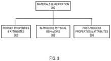
- FIG. 3shows how Materials Qualification can be measured and characterized using multiple factors
- FIG. 4shows two graphs illustrating powder size distributions
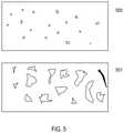
- FIG. 5shows multiple views illustrating the effects of having a concentration of powder having either too great or too small of an overall particle size
- FIG. 6shows schematically different morphologies that will result in different packing and bed density behavior
- FIG. 7shows a single molten track 700 of a nickel-based alloy on an un-melted powder bed
- FIG. 8shows a close up of the interface between the melt track and the unmelted powders indicating a fairly sharp boundary
- FIG. 9shows a highly magnified schematic view showing the microscopic geometry of contact between particles of a powder
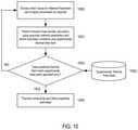
- FIG. 10shows an exemplary block diagram illustrating one possible optimization routine
- FIG. 11shows a chart listing several possible ways of obtaining experimentally determined thermal field data
- FIG. 12shows a block diagram illustrating a method for characterizing and optimizing machine parameters for use with a new lot or batch of powder
- FIG. 13shows exemplary additive manufacturing equipment that includes sensors for monitoring additive manufacturing operations
- FIGS. 14A-14Fshow a series of graphs depicting various bulk and scan level quality metrics
- FIGS. 15A-15Fclearly depict that the peak temperature is higher, the heating rate is lower, and the cooling rate is less negative (slower cooling) for the 50 micron layer as compared to the 40 micron layer;
- FIGS. 16A-16Bshow charts depicting sensor readings of peak temperature for multiple additive machining operations using powders having different particle size distributions
- FIG. 17shows a flow chart depicting a method for carrying out powder reuse after an additive manufacturing operation
- FIGS. 18A-18Fshow charts depicting the heat signature of the powder is it is reused over a number of different additive manufacturing operations.
- FIG. 19shows a test pattern for testing material characteristics of a powder prior to using the powder in a production or production development environment.
- Additive manufacturingwhen performed using a concentrated moving heat source that impinges upon a powder bed, depends on a multitude of attributes and properties that are associated with the powder material itself.
- FIG. 1shows a table enumerating some examples of various material attributes and properties that can impact quality of a part produced by an additive manufacturing process. It is seen that many parameters can have a significant impact on the powder sintering process, and that equivalence of powders is a multi-dimensional, multi-parameter problem. A combination of powder properties, thermophysical properties, and optical properties must be carefully matched to ensure equivalent outcomes. It is instructive to focus on the post-process aspects of the powder sintering process. Equivalence of results or outcome of the Additive Manufacturing process is another key aspect of establishing equivalence of different materials at the input end.
- powder propertiescan include but are not limited to: Particle size distribution; Particle morphology; Particle surface area; Particle chemical composition; Specific contaminate types; State of surface oxidation; and other particle attributes that could impact quality.
- Thermophysical propertiescan include but are not limited to: Powder tap density; Density of a powder bed as put down by spreading mechanism/recoating process before next layer is sintered; Heat capacity of powder bed before sintering (as a composite comprised of powder and gas); Thermal conductivity of powder bed before sintering (as a composite comprised of powder and gas); Surface tension of molten metal during sintering; and Wetting contact angle between molten metal and unmelted powders/powder bed.
- Optical propertiescan include but are not limited to: Optical absorptivity of powder bed before sintering while it is in a solid state; Optical absorptivity of molten liquid; Potential for non-imaging concentration of optical/radiative energy
- FIG. 2shows a table listing different aspects of equivalence in terms of product attributes and post-manufacturing properties.
- the equivalence of powderstherefore implies a combination of properties and attributes enumerated in the tables in FIG. 1 and FIG. 2 as well as metrics relating to the in-process physical behavior of the manufacturing process itself.
- micro-level metallurgical examinationcan include the measurement of any of the following: Grain size; Grain orientation; Grain morphology and growth direction in relation to thermal gradients; Dendrite arm spacing; Secondary dendrite arm spacing; Other microstructural characteristics of interest—precipitates, etc.; Voids and other defects; Cracks; Partially molten zone adjacent to melt track/powder bed interface; and Evidence of liquid infiltration of the powder bed.
- the other post-process characterizations and propertiescan include but not be limited to: Residual stress and distortion; Mechanical properties and other post-process properties.
- FIG. 3shows how Materials Qualification 300 can be measured and characterized using multiple factors. Determining equivalency of powders can be accomplished using one or more of the following: measuring powder properties and attributes 301 prior to initiating a build process, measuring in-process physical behaviors 302 that occur during the manufacturing process, and measuring post-process properties and attributes 303 of the finished article. This description expounds and instructs a detailed methodology by which all three of the aspects of Materials Qualification shown in FIG. 3 are integrally combined.
- the fraction of large and small particleare both important as they can significantly influence behavior during manufacturing. For example, a lot or batch of powder having a large fraction of fine particles in the particle size distribution can result in the fine particles vaporizing during the Additive Manufacturing process, which can create porosity due to material vaporization. At the other extreme, a lot or batch of powder having a large fraction of large particles can result in incomplete melting and fusion for the power density chosen to be optimal with respect to the average (or mean) particle size. This can result in large, irregular porosity due to incomplete fusion, or can result in unfused particles being incorporated into the final manufactured article with the corresponding interfaces between fused and unfused regions.
- View 500 of FIG. 5schematically shows a possible result of using a powder having a large concentration of fine particles. This can result in a relatively smaller porosity made up of numerous substantially spherical pores. This is the result of material vaporization caused by the fine particles receiving enough energy to vaporize.
- View 501shows a result of the use of a lot or batch of powder having a large fraction of large particles. As depicted, this results in relatively larger irregular porosity, which is the result of incomplete particle fusion and/or melting.
- surface area of the particlesplays an important role in the possibility of entrapment or entrainment of contaminants as well as the surface oxidation state of the particles.
- the particle morphologyis another critical factor and can influence the density and packing of the particles in the powder bed prior to sintering or consolidation as part of the Additive Manufacturing process.
- FIG. 6shows schematically different morphologies that will result in different packing and bed density behavior.
- the processinitially has spherical particles as depicted in view 600 with a given particle size distribution, then during the Additive Manufacturing process it is possible for particles to partially or completely agglomerate. This can happen if molten fine particles of molten material are ejected during the Additive Manufacturing process and are re-deposited onto unmelted regions of the powder bed. This can result in spherical particles with so-called satellite particles attached to them, as depicted in view 601 . Both the spherical morphology 601 as well as the spherical with satellite morphology 601 will have different density and packing behavior as compared to irregular particles 602 .
- FIG. 7shows a single molten track 700 of a nickel-based alloy on an un-melted powder bed 701 .
- the melt trackis highly localized and does not have a significant heat affected zone.
- FIG. 8shows a close up of the interface between the melt track and the unmelted powders indicating a fairly sharp boundary, which in turn implies the presence of sharp thermal gradients.
- FIG. 8also shows the presence of a columnar microstructure 800 in the middle of the track indicating solidification in the presence of a strong directional thermal gradient.
- the unmelted zone 801consists of unmelted powders and is fairly sharp due to the low thermal conductivity of the powder bed as compared to the molten liquid or solidified melt track.
- the powder bed conductivityis generally an unknown material property that is difficult to measure directly. However to establish the equivalence of two different powder lots or batches, it is important to verify that their thermal conductivity properties are equivalent. More generally, the thermophysical properties of density, heat capacity and thermal conductivity must be equivalent. As previously mentioned, thermal conductivity in a packed powder bed with interstitial gas is a complex phenomenon.
- FIG. 9shows a highly magnified schematic view showing the microscopic geometry of a powder contact.
- the lines of heat fluxare compressed and flow through the geometric constrictions posed by the microscopic contacts.
- heatis transferred through the interstitial gas pockets. Over the very small distances that characterize such interstitial spaces, the primary mechanism of such heat transfer will be conduction.
- This type of problemcan also be viewed as an optimization problem in which the material parameters are unknown quantities to be determined through an optimization routine.
- FIG. 10shows an exemplary block diagram illustrating one possible optimization routine.
- material parameterssuch as thermal conductivity are chosen initially or are iterated as required in the optimization loop.
- the forward thermal heat transfer problemis solved using the known boundary conditions, known heat input, and assumed thermal properties for the powder bed.
- experimental thermal field datais gathered. The data can be gathered in many ways, including by one or more of the following: by real-time measurements occurring during the manufacturing process; through examination of microstructure after the manufacturing process is complete; at some intermediate state of the manufacturing process; and by examining a specially designed test coupon for this purpose.
- the comparisonis made between the predicted thermal values based on the assumed material properties and the known heat input and boundary conditions in the one hand and the experimental thermal field data on the other hand.
- the results of the predicted thermal fieldmatch the experimentally measured thermal field within a specified error, then at 1004 we have a completed prediction of the thermal properties based on this optimization routine. Otherwise the process reverts back to 1000 and a new set of assumed properties is chosen, and the optimization loop repeats.
- FIG. 11outlines several possible ways of obtaining experimentally determined thermal field data. Generally it can be obtained using real time data from the manufacturing process itself or from post-process metallurgical or metallographic data.
- the table depicted in FIG. 11outlines several possible measurements for each category that can be made to obtain such data.
- FIG. 12shows a block diagram illustrating a method for characterizing and optimizing machine parameters for use with a new lot or batch of powder.
- the new lot or batch of powderis analyzed.
- Various well known methods of analysiscan be used to determine characteristics of the batch of powder such as purity, the particle composition, particle size and particle shape.
- a material characterization processorcan be configured to determine whether the measured characteristics fall within tolerances for the additive manufacturing machine and/or process. When one or more parameters are outside of or exceed a predefined threshold the lot or batch can be returned to the manufacturer or undergo additional processing to achieve acceptable values for the parameters exceeding the predefined thresholds.
- the powdercould be sifted through a series of screens configured to remove particles having sizes that exceed and/or fall below a predefined particle size range.
- a test patterncan be produced using the new lot or batch and a standardized parameter set. Sensor data captured while producing the part can be compared to sensor data captured while producing the same part with a known-good batch of powder using the same standardized parameter set. By comparing the sensor data certain properties and characteristics can be inferred with regards to the new lot or batch of powder.
- production runscan begin. In some embodiments, adjustments to the powder composition and/or measurements taken during the test build process can be used to optimize parameter settings when beginning to conduct product build processes.
- these previous sets of testing and analysis stepscan be sufficient to achieve a successful build process.
- sensors data captured during the production build processcan be compared with sensor data collected during previous known good processing runs. These measurements can be used to adjust parameters such as laser power or scan pattern to arrive at a satisfactory build process.
- a controller responsible for carrying out the build processcan adjust the power settings during the build process to adjust for conditions departing from.
- the build processis refined. The refining can take the form of comparing sensor data recorded during the build process with post-process dissection of the finished part, to identify any potential flaws in the build process occurring as a result of the new batch or lot of powder. In this way, an ideal or at least functional solution can be determined.
- FIG. 13shows exemplary additive manufacturing equipment.
- FIG. 13illustrates additive manufacturing equipment and a quality control system 1300 suitable for use with at least some of the previously described embodiments.
- the quality control system 1300can be utilized in conjunction with Additive Manufacturing processes in which the moving heat source is a laser and the material addition could be either through the sequential pre-placement of layers of metal powders to form a volume of powder 1301 , as depicted, on a powder bed 1302 , or the material addition could be accomplished by selectively placing powder straight into the molten region generated by the moving laser on the part.
- a particle spreader(not depicted) can be configured to deposit thin and uniform layers of powder on powder bed 1302 .
- the volume of powder 1301has several distinct build regions 1303 , which are being built up.
- the buildupis accomplished by the application of the heat source to the material build regions 1303 , which causes the deposited powder in those regions to melt and subsequently solidify into a part having a desired geometry.
- the various regions 1303could be different portions of the same part, or they could represent three entirely different parts, as depicted.
- witness coupon 1304is provided.
- Trust coupon 1304is a standardized volume element, which allows the sampling of every production build and which represents a small and manageable but still representative amount of material which could be destructively tested for metallurgical integrity, physical properties, and mechanical properties.
- the witness coupon 1304also has a layer of material put down concurrent to the layer being processed in the distinct build regions 1303 .
- There is an optical sensor 1305for example a pyrometer, directly interrogating the witness coupon 1304 .
- optical sensor 1305is represented as a pyrometer herein although it will be evident to one of skill in the art that other optical sensors could be utilized as part of a larger optical sensing system.
- the pyrometer 1305is fixed with respect to the powder bed 1302 and collects radiation from a fixed portion of the volume of powder 1301 , i.e., the witness coupon 1304 .
- the radiation observed by pyrometer 1305can be subsequently stored as sensor readings in a computer readable storage medium for real-time or post-process analysis.
- the sensor readingscan be processed by a controller or processor associated with quality control system 1300 .
- computer readable storage mediumcan take the form of a device hard drive capable of storing sensor data from many different additive manufacturing operations.
- the laser source 1306emits a laser beam 1307 that is deflected by a partially reflective mirror 1308 .
- Partially reflective mirror 1308can be configured to reflect only those wavelengths of light that are associated with wavelengths of laser beam 1307 , while allowing other wavelengths of light to pass through partially reflective mirror 1308 .
- laser beam 1307enters scan head 1309 .
- Scan head 1309can include internal x-deflection, y-deflection, and focusing optics.
- the deflected and focused laser beam 1307exits the scan head 1309 and forms a small, hot, travelling melt pool 1310 in the distinct build regions 1303 being melted or sintered layer by layer.
- Scan head 1309can be configured to maneuver laser beam 1307 across a surface of the volume of powder 1301 at high speeds. It should be noted that in some embodiments, laser beam 407 can be activated and deactivated at specific intervals to avoid heating portions of the volume of powder 1301 across which scan head 1309 would otherwise scan laser beam 1307 .
- Melt pool 1310emits optical radiation 1311 that travels back through scan head 1309 and passes through partially reflective mirror 1308 to be collected by optical sensor 1312 .
- the optical sensor 1312collects optical radiation from the travelling melt pool 1310 and therefore, images different portions of the volume of powder 1301 as the melt pool 1310 traverses the volume of powder.
- a sampling rate of optical sensor 1312will generally dictate how many data points can be recorded as melt pool 1310 scans across the volume of powder 1301 .
- the optical sensor 1312can take many forms including that of a photodiode, an infrared camera, a CCD array, a spectrometer, or any other optically sensitive measurement system.
- quality control system 1300can also include optical sensor 1313 .
- Optical sensor 1313can be configured to receive optical information across a wide field of view 1314 so that real time monitoring of substantially all of the volume of powder 1301 can be realized.
- optical sensor 1313can take many forms including that of a photodiode, an infrared camera, a CCD array, and the like.
- readings from pyrometer 1305can be used to calibrate optical sensor 1313 so that heat readings across the entire surface of the volume of powder 1301 can be continuously recorded and analyzed for irregularities. Additionally, quantitative temperature information can be measured at all locations of the volume of powder 1301 using optical sensor 1313 .
- This quality assurance system 1300can be used with any of the described embodiments disclosed herein.
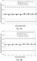
- FIGS. 14A-14Fshow a series of graphs depicting various bulk and scan level quality metrics.
- Bulk quality metricsrepresents sensor readings taken while a heat source is not in the field of view of the sensor
- scan level quality metricsrefer to sensor reading taken while the heat source is passing through the field of view of the sensor (e.g. readings taken within the witness coupon region depicted in FIG. 13 ).
- the specific quality metrics chosen for both bulk and scan level responseare peak temperature (PT), heating rate (HR), and cooling rate (CR). These are representative quality metrics and not by any means the only possible quality metrics which could elucidate the differences shown herein.
- D10, D50, and D90mean that 10%, 50%, and 90% of the particles in the particle size distribution are less than or equal to the corresponding particle size in microns. Therefore they could be viewed as the 10 th , 50 th , and 90 th percentile numbers for the particle size distribution. Furthermore for each type of powder used, the layer thicknesses were adjusted to 40 microns and 50 microns. Identical sets of process parameters were then run on each batch of powder.
- FIGS. 15A-15FFor example looking at the powder with the larger particle size distribution, the difference in layer thickness on three representative scan level features is shown in FIGS. 15A-15F .
- three different sampleswere taken with 100 layers each. The mean values for each sample are shown in the graphs.
- the temperatureswere uncorrected, i.e. they were simply converted from a raw pyrometer/thermal sensor signal, so the measurements are not corrected to compensate for factors such as emissivity variations, phase change, field of view, etc.
- the differences when the data is scaledare not expected to change as the scaling is either linear or monotonically increasing in terms of their effect on the raw data signals, i.e. simple scaling/offset.
- FIGS. 15A-15Fclearly depict that the peak temperature is higher, the heating rate is lower, and the cooling rate is less negative (slower cooling) for the 50 micron layer as compared to the 40 micron layer.
- the thicker layermeans a longer heat conduction length and hence a high peak temperature (longer distance for heat to travel to heat sink).
- the greater amount of material being meltedmeans that the thicker layer will have a slower heating rate for a given set of beam power and travel speed conditions.
- the cooling rateshould be less negative, i.e. the cooling is slower for the thicker material layer. It is interesting to note that the same trend holds for the smaller particle size distribution.
- the samples here tooare samples of 100 layers respectively.
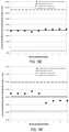
- FIGS. 16A-16Bdepict sensor readings of a sensitive feature, peak temperature.
- FIGS. 16A-16Bdepict sensor readings of a sensitive feature, peak temperature.
- FIGS. 16A-16Bdepict sensor readings of a sensitive feature, peak temperature.
- the effectto be greater for a 50 micron layer thickness as compared to a 40 micron layer thickness because of the greater distance that heat must travel before it can be dissipated through thermal diffusion. Both of these trends are borne out in the data as shown in FIGS. 16A and 16B .
- detectable variationsare not limited to variations in layer thickness and particle size.
- a heavily oxidized powdercould reduce thermal conductivity on account of the oxidized materials being poor conductors of heat.
- Another powder characteristic that can be detected by the described thermal measurement systemsis the presence of contaminates within the powder.
- surface tension of the melted metalcan be determined.
- Variations in surface tensioncan then be mapped to contamination of the powder.
- changes in surface tensioncould give indication of the presence of contaminates within the powder down to the parts per million level. Measurement of surface tension in this manner is described in more detail in application Ser. No. 14/945,249, entitled “Multi-Sensor Quality Inference and Control for Additive Manufacturing Processes.”
- Another powder characteristic that can be detectedis variations in the alloy composition. By measuring the on-heating liquidus temperature of the powder (i.e. melting temperature) of the powder using calibrated temperature data collected by a thermographic sensor, any variation of the melting temperature from the known standard melting temperature for that alloy composition can be a strong indicator of a variation in the alloy composition.
- common variationscan be quickly identified by referencing a chart characterizing likely effects caused by common alloy variations. Once a potential variation is identified further investigation can be performed to determine the actual composition of the alloy, which can then be used to populate the chart with additional data points.
- a manufacturing process cyclecan be carried out.
- any powder unused during the process cyclecan be recovered.
- the recovered powderscan go through a sieving process that purifies and normalizes a particle size distribution of the recovered powders.
- the powdercan again be checked to confirm that the original particle size distribution requirements are met. In some embodiments, this can be carried out as a spot check when little to no variation in the powders is expected.
- the reused powderscan be checked for contamination. This could be done chemically or determined during a follow on build operation using in-process sensor measurements.
- the environmental exposure of the powder over timecan be considered.
- oxidation and/or contaminationcan be checked for more rigorously.
- in-process checks and verificationscan be carried out.
- the powdercan be validated for reuse or flagged as having a potential safety concern. This process can be used in conjunction with any of the other embodiments, described herein.
- the new global meanwould simply be a weighted mean of the individual means, where the weighting factor is the number of observations in each run (sample).
- G sampleswhich in this case are the nine samples depicted in FIGS. 18A-18F .
- s(j)are the individual standard deviations for the individual samples and n(j) is the number of observations in sample j, which again in our case is identical for all samples and is equal to 100.
- n(j)is the number of observations in sample j, which again in our case is identical for all samples and is equal to 100.
- There is another element to the total variance however, and that is deviation between the global mean and the individual means for the individual samples. This deviation is given by: for j in the range[1, G ] DEV ( j )⁇ M ( j ) ⁇ GM ⁇ Eq(5)
- the first set of metrics shown in FIGS. 18A-18Cis more closely related to the response of the powder bed and materials which comprises the powder bed when the laser is not in the immediate field of view of the sensor (i.e. bulk level response).
- thermal response characteristicscan be influenced by variations in material properties such as powder density and thermal conductivity of the powder bed. These properties in turn are influenced by particle size distribution among other powder properties.
- the second set of metricsis extracted from the real time data which are derived from the time intervals when the laser is directly in the field of view of the sensor (i.e. scan level response depicted in FIGS. 18D-18F ). These metrics correspond more directly to the local solidification conditions and are therefore most closely related to as-deposited microstructure and material properties.
- a controller associated with additive manufacturing equipmentcould be configured to flag a problem when the mean scan peak temperature for a particular run exceeds the global plus 1.5 sigma limit. In this way, material reuse can be halted when the powder has undergone too much change on account of going through too many heating and cooling operations.
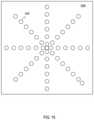
- FIG. 19shows a test configuration that can be used when a new lot or batch of powder is introduced to see if the new powder behaves the same as previous batches of powders.
- test configurationsThere are an infinite variety of such test configurations.
- An example of one such test configurationconsisting of right circular cylinders 1902 .
- Such a trialin addition to the supplied material specifications provided by the supplier, are an important step to verify and validate that the new lot or batch of powders is actually the same when it is run in the AM process, not simply the same on paper and according to the provided specifications. This therefore provides the AM manufacturer an independent means of determining powder equivalence even in the absence of other supporting or corroborating data.
- the test patterncan be more widely varied and include features such as overhangs and channels so that the powder can be evaluated in many different ways.
- test configuration depicted in FIG. 19could also be used to rapidly re-adjust parameters of the process to accommodate differences in particle size distributions or to understand how parameters can be changed so as to compensate for particle size differences.
- the distribution of right circular cylinders 1902 across build plate 1904can also help to identify any performance variations across the build plane.
Landscapes
- Engineering & Computer Science (AREA)
- Chemical & Material Sciences (AREA)
- Materials Engineering (AREA)
- Manufacturing & Machinery (AREA)
- Physics & Mathematics (AREA)
- Plasma & Fusion (AREA)
- Mechanical Engineering (AREA)
- Optics & Photonics (AREA)
- Powder Metallurgy (AREA)
Abstract
Description
| TABLE 1 | |||||
| Smaller Sized Particle Size | Larger Sized Particle Size | ||||
| Distribution | Distribution | ||||
| D10 | 27.9 microns | D10 | 18.9 microns | ||
| D50 | 39.4 microns | D50 | 31.2 microns | ||
| D90 | 57.8 microns | D90 | 47.2 microns | ||
N=Σj=1Gn(j) Eq(1)
ESSG(j)=σj2·{n(j)−1} Eq(3)
ESS=Σj=1GESSG(j)=Σj=1Gσj2·{n(j)−1} Eq(4)
forjin the range[1,G]DEV(j)={M(j)−GM} Eq(5)
GSS(j)={M(j)−GM}2·n(j) Eq(6)
TGSS=σj=1G{M(j)−GM}2·n(j) Eq(7)
σG=√{square root over (GV)} Eq(9)
Claims (19)
Priority Applications (1)
| Application Number | Priority Date | Filing Date | Title |
|---|---|---|---|
| US16/245,369US11267047B2 (en) | 2015-01-13 | 2019-01-11 | Material qualification system and methodology |
Applications Claiming Priority (5)
| Application Number | Priority Date | Filing Date | Title |
|---|---|---|---|
| US201562103034P | 2015-01-13 | 2015-01-13 | |
| US201562235232P | 2015-09-30 | 2015-09-30 | |
| US14/995,183US10226817B2 (en) | 2015-01-13 | 2016-01-13 | Material qualification system and methodology |
| PCT/US2016/013303WO2016115284A1 (en) | 2015-01-13 | 2016-01-13 | Material qualification system and methodology |
| US16/245,369US11267047B2 (en) | 2015-01-13 | 2019-01-11 | Material qualification system and methodology |
Related Parent Applications (1)
| Application Number | Title | Priority Date | Filing Date |
|---|---|---|---|
| US14/995,183ContinuationUS10226817B2 (en) | 2015-01-13 | 2016-01-13 | Material qualification system and methodology |
Publications (2)
| Publication Number | Publication Date |
|---|---|
| US20190143413A1 US20190143413A1 (en) | 2019-05-16 |
| US11267047B2true US11267047B2 (en) | 2022-03-08 |
Family
ID=56406356
Family Applications (1)
| Application Number | Title | Priority Date | Filing Date |
|---|---|---|---|
| US16/245,369ActiveUS11267047B2 (en) | 2015-01-13 | 2019-01-11 | Material qualification system and methodology |
Country Status (4)
| Country | Link |
|---|---|
| US (1) | US11267047B2 (en) |
| EP (1) | EP3245045A4 (en) |
| CN (1) | CN107428081B (en) |
| WO (1) | WO2016115284A1 (en) |
Families Citing this family (19)
| Publication number | Priority date | Publication date | Assignee | Title |
|---|---|---|---|---|
| DE102015017470B4 (en) | 2014-08-22 | 2025-07-17 | Divergent Technologies, Inc. | FAILURE DETECTION FOR ADDITIVE MANUFACTURING SYSTEMS |
| US10786948B2 (en) | 2014-11-18 | 2020-09-29 | Sigma Labs, Inc. | Multi-sensor quality inference and control for additive manufacturing processes |
| CN107428081B (en) | 2015-01-13 | 2020-07-07 | 西格马实验室公司 | Materials identification system and method |
| US10226817B2 (en) | 2015-01-13 | 2019-03-12 | Sigma Labs, Inc. | Material qualification system and methodology |
| US10207489B2 (en) | 2015-09-30 | 2019-02-19 | Sigma Labs, Inc. | Systems and methods for additive manufacturing operations |
| US10386818B2 (en) | 2017-06-09 | 2019-08-20 | Honeywell International Inc. | Quality management systems, methods, and program products for additive manufacturing supply chains |
| CN108152291B (en)* | 2017-11-30 | 2020-02-28 | 清华大学 | Real-time detection method for incomplete fusion of end seam welding based on dynamic characteristics of weld pool |
| KR20210006378A (en)* | 2018-04-23 | 2021-01-18 | 머티어리얼리스 엔브이 | Thermal control of laser sintering |
| DE102018110294A1 (en) | 2018-04-27 | 2019-10-31 | Eos Gmbh Electro Optical Systems | Method and device for generating control data for an additive manufacturing device |
| DE102018127407A1 (en)* | 2018-11-02 | 2020-05-07 | Industrieanlagen-Betriebsgesellschaft Mbh | Process for the preparation and analysis of a powder by means of instrumental analysis and use |
| US11079739B2 (en)* | 2019-02-25 | 2021-08-03 | General Electric Company | Transfer learning/dictionary generation and usage for tailored part parameter generation from coupon builds |
| JP6864858B2 (en)* | 2019-03-04 | 2021-04-28 | 日立金属株式会社 | Ni-based corrosion-resistant alloy powder for laminated molding, manufacturing method of laminated molded products using this powder |
| US11472115B2 (en) | 2019-03-21 | 2022-10-18 | General Electric Company | In-situ monitoring system assisted material and parameter development for additive manufacturing |
| JP6734447B1 (en)* | 2019-07-31 | 2020-08-05 | 株式会社ソディック | Material powder for metal additive manufacturing and manufacturing method thereof |
| FR3111575A1 (en)* | 2020-06-23 | 2021-12-24 | Safran Aircraft Engines | Powder bed additive manufacturing process |
| US11638959B2 (en) | 2020-09-03 | 2023-05-02 | General Electric Company | Systems and methods for estimating powder dosing in additive manufacturing processes |
| EP4274730A4 (en)* | 2021-03-09 | 2024-09-04 | Hewlett-Packard Development Company, L.P. | Determining powder degradation |
| US12030119B2 (en) | 2021-03-31 | 2024-07-09 | Baker Hughes Oilfield Operations Llc | In-situ powder witness coupon |
| CN118664910A (en)* | 2024-08-22 | 2024-09-20 | 西安空天机电智能制造有限公司 | 3D printing equipment and 3D printing control method |
Citations (200)
| Publication number | Priority date | Publication date | Assignee | Title |
|---|---|---|---|---|
| US3499310A (en) | 1968-05-27 | 1970-03-10 | Alcor Aviat | Self-calibrating temperature sensing probe and probe - indicator combination |
| US3992615A (en) | 1975-05-14 | 1976-11-16 | Sun Studs, Inc. | Electro-optical ranging system for distance measurements to moving targets |
| US4041476A (en) | 1971-07-23 | 1977-08-09 | Wyn Kelly Swainson | Method, medium and apparatus for producing three-dimensional figure product |
| US4247508A (en) | 1979-12-03 | 1981-01-27 | Hico Western Products Co. | Molding process |
| US4323756A (en) | 1979-10-29 | 1982-04-06 | United Technologies Corporation | Method for fabricating articles by sequential layer deposition |
| US4423287A (en) | 1981-06-26 | 1983-12-27 | Visa U.S.A., Inc. | End-to-end encryption system and method of operation |
| US4575330A (en) | 1984-08-08 | 1986-03-11 | Uvp, Inc. | Apparatus for production of three-dimensional objects by stereolithography |
| US4863538A (en) | 1986-10-17 | 1989-09-05 | Board Of Regents, The University Of Texas System | Method and apparatus for producing parts by selective sintering |
| US5272027A (en) | 1992-06-11 | 1993-12-21 | Eastman Kodak Company | Method of monitoring the preparation of a photographic emulsion by conductivity measurements |
| US5412730A (en) | 1989-10-06 | 1995-05-02 | Telequip Corporation | Encrypted data transmission system employing means for randomly altering the encryption keys |
| US5487011A (en) | 1994-03-17 | 1996-01-23 | Gerber Garment Technology, Inc. | Garment marker system having computer assisted alignment of variable contrast cloth designs |
| US5737090A (en) | 1993-02-25 | 1998-04-07 | Ohio Electronic Engravers, Inc. | System and method for focusing, imaging and measuring areas on a workpiece engraved by an engraver |
| US5956408A (en) | 1994-09-15 | 1999-09-21 | International Business Machines Corporation | Apparatus and method for secure distribution of data |
| US5962065A (en) | 1995-12-15 | 1999-10-05 | Micron Technology, Inc. | Method of forming polysilicon having a desired surface roughness |
| US6058193A (en) | 1996-12-23 | 2000-05-02 | Pitney Bowes Inc. | System and method of verifying cryptographic postage evidencing using a fixed key set |
| US6112187A (en) | 1997-05-20 | 2000-08-29 | Any Co., Ltd. | Encryption communication system for generating passwords on the basis of start information on both parties of communication |
| US6261493B1 (en)* | 1997-03-20 | 2001-07-17 | Therics, Inc. | Fabrication of tissue products with additives by casting or molding using a mold formed by solid free-form methods |
| US6357910B1 (en) | 1999-08-04 | 2002-03-19 | Photosonic, Inc. | Multiwavelength pyrometer for measurement in hostile environments |
| US20020095234A1 (en) | 1999-06-29 | 2002-07-18 | Nikon Corporation | Marke detection method and unit, exposure method and apparatus, and device manufacturing method and device |
| US6483596B1 (en) | 1999-04-23 | 2002-11-19 | Eos Gmbh Electro Optical Systems | Method of calibrating an apparatus for producing a three-dimensional object, calibration apparatus and method and apparatus for producing a three-dimensional object |
| US20020184511A1 (en) | 1997-05-08 | 2002-12-05 | Kolouch James L. | Secure accounting and operational control reporting system |
| US6547994B1 (en)* | 1998-11-13 | 2003-04-15 | Therics, Inc. | Rapid prototyping and manufacturing process |
| US6554600B1 (en) | 1998-10-09 | 2003-04-29 | Eos Gmbh Electro Optical Systems | Device for producing a three-dimensional object, especially a laser sintering machine |
| US20030084292A1 (en) | 2001-10-22 | 2003-05-01 | Pierce Shaun D. | Using atomic messaging to increase the security of transferring data across a network |
| US20030151167A1 (en)* | 2002-01-03 | 2003-08-14 | Kritchman Eliahu M. | Device, system and method for accurate printing of three dimensional objects |
| US6633391B1 (en) | 2000-11-07 | 2003-10-14 | Applied Materials, Inc | Monitoring of film characteristics during plasma-based semi-conductor processing using optical emission spectroscopy |
| US20030212894A1 (en) | 2002-05-10 | 2003-11-13 | Peter Buck | Authentication token |
| US6649310B2 (en) | 2000-08-30 | 2003-11-18 | Kabushiki Kaisha Toshiba | Method of manufacturing photomask |
| US6667700B1 (en) | 2002-10-30 | 2003-12-23 | Nbt Technology, Inc. | Content-based segmentation scheme for data compression in storage and transmission including hierarchical segment representation |
| US6672343B1 (en) | 1999-06-21 | 2004-01-06 | Eos Gmbh Optical Systems | Device for supplying powder for a device for producing a three-dimensional object layer by layer |
| US20040034783A1 (en) | 2002-08-15 | 2004-02-19 | Fedronic Dominique Louis, Joseph | System and method for sequentially processing a biometric sample |
| EP1466718A2 (en) | 2003-04-09 | 2004-10-13 | 3D Systems, Inc. | Sintering using thermal image feedback |
| US6824714B1 (en) | 1999-08-20 | 2004-11-30 | Eos Gmbh Electro Optical Systems | Device and method for generative production of a three-dimensional object |
| US20050069171A1 (en) | 1999-05-19 | 2005-03-31 | Rhoads Geoffrey B. | Embedded data in gaming objects for authentication and association of behavior information |
| US20050133527A1 (en) | 1999-07-07 | 2005-06-23 | Optomec Design Company | Powder feeder for material deposition systems |
| US20050137983A1 (en) | 2003-12-18 | 2005-06-23 | Matthew Bells | System and method for digital rights management |
| US20050134188A1 (en) | 2003-12-22 | 2005-06-23 | Nokia Corporation | Apparatus and method for producing variable intensity of light |
| US20050140964A1 (en) | 2002-09-20 | 2005-06-30 | Laurent Eschenauer | Method and apparatus for key management in distributed sensor networks |
| US20050154923A1 (en) | 2004-01-09 | 2005-07-14 | Simon Lok | Single use secure token appliance |
| US20050166263A1 (en) | 2003-09-12 | 2005-07-28 | Andrew Nanopoulos | System and method providing disconnected authentication |
| US6930278B1 (en) | 2004-08-13 | 2005-08-16 | 3D Systems, Inc. | Continuous calibration of a non-contact thermal sensor for laser sintering |
| US6932935B1 (en) | 1999-08-06 | 2005-08-23 | Eos Gmbh Electro Optical Systems | Method and device for producing a three-dimensional object |
| US20050190914A1 (en) | 2004-02-27 | 2005-09-01 | Microsoft Corporation | Counterfeit and tamper resistant labels with randomly occurring features |
| US6996722B1 (en) | 1997-12-19 | 2006-02-07 | British Telecommunications Public Limited Company | Data communications |
| US7011247B2 (en) | 2000-03-15 | 2006-03-14 | Axalto Sa | Method of communication between a smart card and a host station |
| US20060075254A1 (en) | 2004-09-27 | 2006-04-06 | Cisco Technology, Inc. (A California Corporation) | Smart card functionality from a security co-processor and symmetric key in ROM |
| US7069439B1 (en) | 1999-03-05 | 2006-06-27 | Hewlett-Packard Development Company, L.P. | Computing apparatus and methods using secure authentication arrangements |
| US20060149407A1 (en) | 2001-12-28 | 2006-07-06 | Kimberly-Clark Worlwide, Inc. | Quality management and intelligent manufacturing with labels and smart tags in event-based product manufacturing |
| EP1700686A2 (en) | 2005-03-09 | 2006-09-13 | 3D Systems, Inc. | Laser sintering powder recycle system |
| US20060229744A1 (en) | 2005-03-15 | 2006-10-12 | Mitutoyo Corporation | Operator interface apparatus and method for displacement transducer with selectable detector area |
| US7127304B1 (en)* | 2005-05-18 | 2006-10-24 | Infineon Technologies Richmond, Lp | System and method to predict the state of a process controller in a semiconductor manufacturing facility |
| US20060255158A1 (en) | 2005-05-10 | 2006-11-16 | Yanki Margalit | Security card apparatus |
| US20060287965A1 (en) | 2005-06-15 | 2006-12-21 | E.E. System Corporation | Method and system for real time online debit transactions |
| US20060288216A1 (en) | 2003-03-04 | 2006-12-21 | Peter Buhler | Long-term secure digital signatures |
| US7153463B2 (en) | 2001-02-07 | 2006-12-26 | Eos Gmbh Electro Optical Systems | Device for treating powder for a device which produces a three-dimensional object device for producing a three-dimensional object and method for the production thereof |
| US20070067833A1 (en) | 2005-09-20 | 2007-03-22 | Colnot Vincent C | Methods and Apparatus for Enabling Secure Network-Based Transactions |
| US20070066398A1 (en) | 2005-09-22 | 2007-03-22 | Earl Rowan | Cashless gaming system and method |
| US7213766B2 (en) | 2003-11-17 | 2007-05-08 | Dpd Patent Trust Ltd | Multi-interface compact personal token apparatus and methods of use |
| US20070143227A1 (en) | 2003-06-10 | 2007-06-21 | Kranzley Arthur D | Systems and methods for conducting secure payment transactions using a formatted data structure |
| US20070150942A1 (en) | 2005-12-23 | 2007-06-28 | Cartmell Brian R | Centralized identity verification and/or password validation |
| US20070262138A1 (en) | 2005-04-01 | 2007-11-15 | Jean Somers | Dynamic encryption of payment card numbers in electronic payment transactions |
| US20080127186A1 (en)* | 2006-07-27 | 2008-05-29 | Hemant Kanodia | System for analyzing batch processes |
| US20080148057A1 (en) | 2006-12-19 | 2008-06-19 | Ohanae, Inc. | Security token |
| US20080172738A1 (en) | 2007-01-11 | 2008-07-17 | Cary Lee Bates | Method for Detecting and Remediating Misleading Hyperlinks |
| US7419632B2 (en) | 2002-08-09 | 2008-09-02 | Eos Gmbh Electro Optical Systems | Method and device for the production of a three-dimensional object by means of sintering |
| US7430668B1 (en) | 1999-02-15 | 2008-09-30 | Hewlett-Packard Development Company, L.P. | Protection of the configuration of modules in computing apparatus |
| US20080262659A1 (en) | 2007-04-20 | 2008-10-23 | The Boeing Company | Methods and systems for controlling and adjusting heat distribution over a part bed |
| US20090060184A1 (en) | 2002-10-15 | 2009-03-05 | Alten Alex I | Systems and Methods for Providing Autonomous Security |
| US20090206065A1 (en)* | 2006-06-20 | 2009-08-20 | Jean-Pierre Kruth | Procedure and apparatus for in-situ monitoring and feedback control of selective laser powder processing |
| US7601422B2 (en) | 2002-12-02 | 2009-10-13 | Eos Gmbh Electro Optical Systems | Rounded-particle plastic powder in particular for application in laser sintering, method for production of such a powder and laser sintering process using such a powder |
| US7627386B2 (en) | 2004-10-07 | 2009-12-01 | Zonaire Medical Systems, Inc. | Ultrasound imaging system parameter optimization via fuzzy logic |
| US7628600B2 (en) | 2006-11-22 | 2009-12-08 | Eos Gmbh Electro Optical Systems | Device for a layerwise manufacturing of a three-dimensional object |
| US20090312851A1 (en)* | 2005-07-25 | 2009-12-17 | Biogen Idec Ma Inc. | System and Method for Bioprocess Control |
| US20090313318A1 (en) | 2008-06-13 | 2009-12-17 | Dye Thomas A | System and method using interpretation filters for commercial data insertion into mobile computing devices |
| US20100017867A1 (en) | 2002-10-08 | 2010-01-21 | Koolspan, Inc. | Self-management network access using localized access management |
| US20100024024A1 (en) | 2006-06-16 | 2010-01-28 | Fmt Worldwide Pty Ltd | Authentication System and Process |
| US7661948B2 (en) | 2006-11-22 | 2010-02-16 | Eos Gmbh Electro Optical Systems | Application device for applying a layer of a building material in powder form in a device for a layerwise manufacturing of a three-dimensional object |
| US7665979B2 (en) | 2002-08-02 | 2010-02-23 | Eos Gmbh Electro Optical Systems | Device and method for the production of three-dimensional objects by means of generative production method |
| US7674107B2 (en) | 2006-11-22 | 2010-03-09 | Eos Gmbh Electro Optical Systems | Building container for a device and method for a layerwise manufacturing of a three-dimensional object |
| US20100077216A1 (en) | 2008-09-22 | 2010-03-25 | Bespoke Innovations S.A.R.L. | Method for enhancing network application security |
| US7686605B2 (en) | 2006-11-22 | 2010-03-30 | Eos Gmbh Electro Optical Systems | Device for a layerwise manufacturing of a three-dimensional object |
| US20100098835A1 (en) | 2008-10-20 | 2010-04-22 | 3D Systems, Incorporated | Compensation of Actinic Radiation Intensity Profiles for Three-Dimensional Modelers |
| US7713048B2 (en) | 2006-11-22 | 2010-05-11 | Eos Gmbh Electro Optical Systems | Device for a layerwise manufacturing of a three-dimensional object |
| US7740683B2 (en) | 2003-09-17 | 2010-06-22 | Eos Gmbh Electro Optical Systems | Powder for manufacturing precious metal products by free forming fabrication and products |
| US20100161102A1 (en) | 2008-12-02 | 2010-06-24 | Eos Gmbh Electro Optical Systems | Method of providing an identifiable powder amount and method of manufacturing an object |
| US20100221012A1 (en) | 2007-03-12 | 2010-09-02 | National Institute Of Information And Communication Technology | Burst mode rare earth-doped fiber amplifier |
| US7818129B2 (en) | 2004-08-04 | 2010-10-19 | Agilent Technologies, Inc. | Detection of feature boundary pixels during array scanning |
| US7820241B2 (en) | 2005-04-12 | 2010-10-26 | Eos Gmbh Electro Optical Systems | Device and method for applying layers of a powder material onto a surface |
| US20100280666A1 (en) | 2008-01-10 | 2010-11-04 | Oscar Marchetto | Operating system for roller blinds with protection against excessive wind |
| US20100289627A1 (en) | 2005-08-19 | 2010-11-18 | Adasa Inc. | Fully Secure Item-Level Tagging |
| US7837458B2 (en) | 2006-11-22 | 2010-11-23 | Eos Gmbh Electro Optical Systems | Device for a layer-wise manufacturing of a three-dimensional object |
| US7847057B2 (en) | 2007-04-05 | 2010-12-07 | Eos Gmbh Electro Optical Systems | PAEK powder, in particular for the use in a method for a layer-wise manufacturing of a three-dimensional object, as well as method for producing it |
| US7850885B2 (en) | 2005-05-13 | 2010-12-14 | Eos Gmbh Optical Systems | Device and method for manufacturing a three-dimensional object with a heated recoater for a building material in powder form |
| US7874010B1 (en) | 2003-10-24 | 2011-01-18 | Oracle America, Inc. | Method and apparatus for using secret keys to make data permanently unreadable |
| US7891095B2 (en) | 2003-09-17 | 2011-02-22 | Eos Gmbh Electro Optical Systems | Method of producing jewelry and other precious metal products with complex geometries |
| US20110046766A1 (en)* | 2008-03-25 | 2011-02-24 | Trumpf Maschinen Gruesch Ag | Method for creating numerical control programs |
| US20110052927A1 (en)* | 2008-03-14 | 2011-03-03 | Valspar Sourcing, Inc. | Powder Compositions and Methods of Manufacturing Articles Therefrom |
| US7931462B2 (en) | 2006-05-18 | 2011-04-26 | Eos Gmbh Electro Optical Systems | Device and method for the manufacturing of a three-dimensional object |
| US20110103586A1 (en) | 2008-07-07 | 2011-05-05 | Nobre Tacito Pereira | System, Method and Device To Authenticate Relationships By Electronic Means |
| US7946840B2 (en) | 2006-11-22 | 2011-05-24 | Eos Gmbh Electro Optical Systems | Device and method for a layerwise manufacturing of a three-dimensional object |
| US20110154467A1 (en) | 2009-12-18 | 2011-06-23 | Sabre Inc. | Tokenized data security |
| US20110155905A1 (en) | 2008-04-11 | 2011-06-30 | Ebara Corporation | Specimen observation method and device, and inspection method and device using the method and device |
| US7976302B2 (en) | 2006-11-22 | 2011-07-12 | Eos Gmbh Electro Optical Systems | Device for a layerwise manufacturing of a three-dimensional object and method for inserting and removing respectively, a container |
| US20110191592A1 (en) | 2010-01-29 | 2011-08-04 | Norman Frank Goertzen | Secure Access by a User to a Resource |
| US20110197070A1 (en) | 2010-02-10 | 2011-08-11 | Authernative, Inc. | System and method for in- and out-of-band multi-factor server-to-user authentication |
| US20110196525A1 (en)* | 2010-02-11 | 2011-08-11 | Monosol Rx, Llc | Method and system for optimizing film production and minimizing film scrap |
| US20110237224A1 (en) | 2009-10-23 | 2011-09-29 | Apriva, Llc | System and device for facilitating remote invocation of personal token capabilities |
| US8031384B2 (en) | 2006-11-22 | 2011-10-04 | Eos Gmbh Electro Optical Systems | Device for a layerwise manufacturing of a three-dimensional object and method for adjusting an optical system of the same |
| US8034279B2 (en) | 2007-03-27 | 2011-10-11 | Eos Gmbh Electro Optical Systems | Method and device for manufacturing a three-dimensional object |
| US8073315B2 (en) | 2005-05-26 | 2011-12-06 | Eos Gmbh Electro Optical Systems | Radiant heater for heating the building material in a laser sintering device |
| US8075814B2 (en) | 2005-07-21 | 2011-12-13 | Eos Gmbh Electro Optical Systems | Device for layerwise manufacturing of a three-dimensional object |
| US8078593B1 (en) | 2008-08-28 | 2011-12-13 | Infineta Systems, Inc. | Dictionary architecture and methodology for revision-tolerant data de-duplication |
| US20110307699A1 (en) | 2009-03-25 | 2011-12-15 | Pacid Technologies, Llc | Token for securing communication |
| US8083513B2 (en) | 2006-11-22 | 2011-12-27 | Eos Gmbh Electro Optical Systems | Apparatus for manufacturing a three-dimensional object layer by layer |
| US8121295B1 (en) | 2008-03-28 | 2012-02-21 | Sprint Spectrum L.P. | Method, apparatus, and system for controlling playout of media |
| US8124192B2 (en) | 2007-06-25 | 2012-02-28 | Eos Gmbh Electro Optical Systems | Layer application device for an electrostatic layer application of a building material in powder form and device and method for manufacturing a three-dimensional object |
| US20120060025A1 (en) | 2004-04-15 | 2012-03-08 | Aol Inc. | Service provider invocation |
| US8137739B2 (en) | 2005-04-06 | 2012-03-20 | Eos Gmbh Electro Optical Systems | Apparatus and method for the manufacture of a three-dimensional object |
| US8151345B1 (en) | 2007-01-25 | 2012-04-03 | Yeager C Douglas | Self-authorizing devices |
| US20120110318A1 (en) | 2010-11-02 | 2012-05-03 | Computer Associates Think, Inc. | System and method for controlling state tokens |
| US8172562B2 (en) | 2002-08-02 | 2012-05-08 | Eos Gmbh Electro Optical Systems | Device and method for producing a three-dimensional object by means of a generative production method |
| US20120122252A1 (en) | 2010-11-09 | 2012-05-17 | Yoshihiko Fujimori | Method for inspecting substrate, substrate inspection apparatus, exposure system, and method for producing semiconductor device |
| US20120123581A1 (en) | 2010-11-12 | 2012-05-17 | Asml Netherlands B.V. | Metrology Method and Inspection Apparatus, Lithographic System and Device Manufacturing Method |
| US8186990B2 (en) | 2006-11-22 | 2012-05-29 | Eos Gmbh Electro Optical Systems | Device for a layerwise manufacturing of a three-dimensional object |
| US20120179952A1 (en) | 2009-08-14 | 2012-07-12 | Pim Theo Tuyls | Physically unclonable function with tamper prevention and anti-aging system |
| US20120203700A1 (en) | 2010-12-10 | 2012-08-09 | Electronic Payment Exchange | Tokenized contactless payments for mobile devices |
| US8303886B2 (en) | 2007-12-21 | 2012-11-06 | Eos Gmbh Electro Optical Systems | Method of manufacturing a three-dimensional object |
| US8307210B1 (en) | 2008-05-02 | 2012-11-06 | Emc Corporation | Method and apparatus for secure validation of tokens |
| US8313087B2 (en) | 2004-03-21 | 2012-11-20 | Eos Gmbh Electro Optical Systems | Powder for rapid prototyping and associated production method |
| US8317508B2 (en) | 2008-10-13 | 2012-11-27 | Eos Gmbh Electro Optical Systems | Frame for a device for manufacturing a three-dimensional object and device for manufacturing a three-dimensional object by such a frame |
| US8366432B2 (en) | 2006-11-22 | 2013-02-05 | Eos Gmbh Electro Optical Systems | Device for a layerwise manufacturing of a three-dimensional object |
| WO2013021173A1 (en) | 2011-08-05 | 2013-02-14 | Loughborough University | Methods and apparatus for selectively combining particulate material |
| US20130047263A1 (en) | 2011-08-15 | 2013-02-21 | Bank Of America Corporation | Method and Apparatus for Emergency Session Validation |
| WO2013044047A1 (en) | 2011-09-23 | 2013-03-28 | Stratasys, Inc. | Layer transfusion for additive manufacturing |
| US20130083324A1 (en) | 2011-09-30 | 2013-04-04 | 3M Innovative Properties Company | Web inspection calibration system and related methods |
| US20130085944A1 (en) | 2011-09-29 | 2013-04-04 | Pacid Technologies, Llc | System and method for application security |
| US8414281B2 (en) | 2005-06-27 | 2013-04-09 | Eos Gmbh Electro Optical Systems | Method and device for producing a 3D object by means of a generative 3D-method |
| US8420001B2 (en) | 2008-05-20 | 2013-04-16 | Eos Gmbh Electro Optical Systems | Influencing specific mechanical properties of three-dimensional objects manufactured by a selective sintering by means of electromagnetic radiation from a powder comprising at least one polymer or copolymer |
| US20130114082A1 (en)* | 2010-07-20 | 2013-05-09 | The Regents Of The University Of California | Temperature response sensing and classification of analytes with porous optical films |
| US20130159195A1 (en) | 2011-12-16 | 2013-06-20 | Rawllin International Inc. | Authentication of devices |
| US8501075B2 (en) | 2009-11-25 | 2013-08-06 | Eos Gmbh Electro Optical Systems | Method for manufacturing a three-dimensional object |
| US20130217154A1 (en) | 2010-10-26 | 2013-08-22 | Kazuhiko Fukazawa | Inspection apparatus, inspection method, exposure method, and method for manufacturing semiconductor device |
| US20130226815A1 (en) | 2010-11-10 | 2013-08-29 | Smart Hub Pte. Ltd. | Method of performing a financial transaction via unsecured public telecommunication infrastructure and an apparatus for same |
| US8525071B2 (en) | 2008-07-03 | 2013-09-03 | Eos Gmbh Electro Optical Systems | Apparatus for manufacturing a three-dimensional object layer by layer |
| WO2013128416A2 (en) | 2012-03-02 | 2013-09-06 | Legor Group S.P.A. | Silver-based alloy powder for manufacturing of 3-dimensional metal objects |
| US8554356B2 (en) | 2006-10-06 | 2013-10-08 | Ebara Corporation | Processing end point detection method, polishing method, and polishing apparatus |
| US20130290719A1 (en) | 2011-01-13 | 2013-10-31 | Infosys Limited | System and method for accessing integrated applications in a single sign-on enabled enterprise solution |
| WO2013159811A1 (en) | 2012-04-24 | 2013-10-31 | Arcam Ab | Safety protection method and apparatus for additive manufacturing device |
| US20130309121A1 (en)* | 2012-05-16 | 2013-11-21 | Crucible Intellectual Property Llc | Layer-by-layer construction with bulk metallic glasses |
| US20130326602A1 (en) | 2011-02-22 | 2013-12-05 | Hewlett-Packard Development Company, L.P. | Digital Signatures |
| US20130343947A1 (en) | 2011-01-28 | 2013-12-26 | MTU Aero Engines AG | Method and device for process monitoring |
| US20140004817A1 (en) | 2012-06-29 | 2014-01-02 | Andrew Horton | Cell phone detection and alert information system |
| US20140004626A1 (en)* | 2012-06-30 | 2014-01-02 | Applied Materials, Inc. | Temperature control of chemical mechanical polishing |
| US20140019752A1 (en) | 2012-07-10 | 2014-01-16 | Verizon Patent And Licensing Inc. | Encryption-based session establishment |
| US20140019364A1 (en) | 2010-01-12 | 2014-01-16 | Simon Hurry | Anytime validation tokens |
| US20140039662A1 (en)* | 2012-07-31 | 2014-02-06 | Makerbot Industries, Llc | Augmented three-dimensional printing |
| US8658078B2 (en) | 2006-05-18 | 2014-02-25 | Eos Gmbh Electro Optical Systems | Device and method for a layerwise manufacturing of a three-dimensional object from a building material in powder form |
| US20140082366A1 (en) | 2012-09-14 | 2014-03-20 | Sap Ag | Multi-system security integration |
| US8710144B2 (en) | 2004-03-21 | 2014-04-29 | Eos Gmbh Electro Optical Systems | Powder for layerwise manufacturing of objects |
| US20140163717A1 (en) | 2012-11-08 | 2014-06-12 | Suman Das | Systems and methods for additive manufacturing and repair of metal components |
| US20140183765A1 (en)* | 2010-09-27 | 2014-07-03 | The Texas A&M University System | Ceramic-ceramic composites and process therefor, nuclear fuels formed thereby, and nuclear reactor systems and processes operated therewith |
| US8784721B2 (en) | 2007-11-27 | 2014-07-22 | Eos Gmbh Electro Optical Systems | Method of manufacturing three-dimensional objects by laser sintering |
| US8784720B2 (en) | 2010-02-23 | 2014-07-22 | Eos Gmbh Electro Optical Systems | Method and device for manufacturing a three-dimensional object that is suitable for application to microtechnology |
| US8803073B2 (en) | 2009-04-06 | 2014-08-12 | Eos Gmbh Electro Optical Systems | Method and device for calibrating an irradiation device |
| US20140265046A1 (en)* | 2013-03-15 | 2014-09-18 | Matterfab Corp. | Laser sintering apparatus and methods |
| US20140283104A1 (en)* | 2013-03-13 | 2014-09-18 | Intertrust Technologies Corporation | Object Rendering Systems and Methods |
| WO2014159758A1 (en) | 2013-03-14 | 2014-10-02 | Drs Rsta, Inc. | System architecture for thermal imaging and thermography cameras |
| DE102013206542A1 (en) | 2013-04-12 | 2014-10-16 | Matthias Fockele | Powder processing device |
| US20140332507A1 (en)* | 2011-11-29 | 2014-11-13 | Matthias Fockele | Process for producing a shaped body by layerwise buildup from material powder |
| US20150024233A1 (en) | 2013-07-19 | 2015-01-22 | The Boeing Company | Quality control of additive manufactured parts |
| US20150034606A1 (en)* | 2013-08-02 | 2015-02-05 | Rolls-Royce Plc | Method of manufacturing a component |
| US20150061170A1 (en)* | 2013-09-02 | 2015-03-05 | Thomas Engel | Method and arrangement for producing a workpiece by using additive manufacturing techniques |
| US20150104802A1 (en)* | 2013-10-11 | 2015-04-16 | Paul Reep | Systems and methods for developing quantifiable material standards for feedstocks and products used in additive manufactruing processes |
| US20150128243A1 (en) | 2012-03-08 | 2015-05-07 | Oltio (Proprietary) Limited | Method of authenticating a device and encrypting data transmitted between the device and a server |
| US20150147424A1 (en) | 2013-11-22 | 2015-05-28 | Charles Bibas | 3d printing apparatus with sensor device |
| US20150177158A1 (en) | 2013-12-13 | 2015-06-25 | General Electric Company | Operational performance assessment of additive manufacturing |
| EP2918395A1 (en) | 2014-03-12 | 2015-09-16 | Rolls-Royce Corporation | Additive manufacturing including layer-by-layer imaging |
| US20150268099A1 (en) | 2014-03-24 | 2015-09-24 | James Eldon Craig | Additive manufacturing temperature controller/sensor apparatus and method of use thereof |
| US20150321422A1 (en) | 2014-05-09 | 2015-11-12 | United Technologies Corporation | Sensor fusion for powder bed manufacturing process control |
| US20150375456A1 (en) | 2014-06-30 | 2015-12-31 | General Electric Company | Systems and methods for monitoring a melt pool using a dedicated scanning device |
| US20160005566A1 (en) | 2014-06-20 | 2016-01-07 | California Institute Of Technology | Method and system for electron microscope with multiple cathodes |
| US9271110B1 (en) | 2012-07-09 | 2016-02-23 | Sprint Communications Company L.P. | Location awareness session management and cross application session management |
| US20160098825A1 (en) | 2014-10-05 | 2016-04-07 | Sigma Labs, Inc. | Feature extraction method and system for additive manufacturing |
| WO2016081651A1 (en) | 2014-11-18 | 2016-05-26 | Sigma Labs, Inc. | Multi-sensor quality inference and control for additive manufacturing processes |
| US20160176114A1 (en) | 2014-12-17 | 2016-06-23 | National Applied Research Laboratories | System for online monitoring powder-based 3d printing processes and method thereof |
| US20160184893A1 (en) | 2014-08-22 | 2016-06-30 | Sigma Labs, Inc. | Method and system for monitoring additive manufacturing processes |
| US20160193696A1 (en)* | 2013-08-22 | 2016-07-07 | Renishaw Plc | Apparatus and methods for building objects by selective solidification of powder material |
| US20160199911A1 (en) | 2015-01-13 | 2016-07-14 | Sigma Labs, Inc. | Material qualification system and methodology |
| WO2016115284A1 (en) | 2015-01-13 | 2016-07-21 | Sigma Labs, Inc. | Material qualification system and methodology |
| US20160236279A1 (en) | 2013-09-23 | 2016-08-18 | Renishaw Plc | Additive manufacturing apparatus and method |
| US20160332381A1 (en) | 2014-01-24 | 2016-11-17 | United Technologies Corporation | Monitoring material soldification byproducts during additive manufacturing |
| US20160349724A1 (en)* | 2014-01-16 | 2016-12-01 | Hewlett-Packard Development Company, L.P. | Processing slice data |
| US20170090462A1 (en) | 2015-09-30 | 2017-03-30 | Sigma Labs, Inc. | Systems and methods for additive manufacturing operations |
| US20170097280A1 (en) | 2014-03-28 | 2017-04-06 | United Technologies Corporation | Material testing apparatus and method |
| US20170113415A1 (en) | 2014-06-20 | 2017-04-27 | Carbon, Inc. | Three-Dimensional Printing Method Using Increased Light Intensity and Apparatus Therefore |
| EP3200973A1 (en) | 2014-10-03 | 2017-08-09 | Hewlett-Packard Development Company, L.P. | Controlling temperature in an apparatus for generating a three-dimensional object |
| EP3221076A1 (en) | 2014-11-18 | 2017-09-27 | Sigma Labs, Inc. | Multi-sensor quality inference and control for additive manufacturing processes |
| US9860245B2 (en) | 2009-02-19 | 2018-01-02 | Secure Technologies Inc. | System and methods for online authentication |
| US20180036949A1 (en) | 2015-04-30 | 2018-02-08 | Hewlett-Packard Development Company, L.P. | Misalignment detection for a 3d printing device |
| US9911117B1 (en) | 2002-03-25 | 2018-03-06 | Jpmorgan Chase Bank, N.A. | Systems and methods for time variable financial authentication |
- 2016
- 2016-01-13CNCN201680010333.XApatent/CN107428081B/enactiveActive
- 2016-01-13WOPCT/US2016/013303patent/WO2016115284A1/ennot_activeCeased
- 2016-01-13EPEP16737843.9Apatent/EP3245045A4/enactivePending
- 2019
- 2019-01-11USUS16/245,369patent/US11267047B2/enactiveActive
Patent Citations (217)
| Publication number | Priority date | Publication date | Assignee | Title |
|---|---|---|---|---|
| US3499310A (en) | 1968-05-27 | 1970-03-10 | Alcor Aviat | Self-calibrating temperature sensing probe and probe - indicator combination |
| US4041476A (en) | 1971-07-23 | 1977-08-09 | Wyn Kelly Swainson | Method, medium and apparatus for producing three-dimensional figure product |
| US3992615A (en) | 1975-05-14 | 1976-11-16 | Sun Studs, Inc. | Electro-optical ranging system for distance measurements to moving targets |
| US4323756A (en) | 1979-10-29 | 1982-04-06 | United Technologies Corporation | Method for fabricating articles by sequential layer deposition |
| US4247508B1 (en) | 1979-12-03 | 1996-10-01 | Dtm Corp | Molding process |
| US4247508A (en) | 1979-12-03 | 1981-01-27 | Hico Western Products Co. | Molding process |
| US4423287A (en) | 1981-06-26 | 1983-12-27 | Visa U.S.A., Inc. | End-to-end encryption system and method of operation |
| US4575330A (en) | 1984-08-08 | 1986-03-11 | Uvp, Inc. | Apparatus for production of three-dimensional objects by stereolithography |
| US4575330B1 (en) | 1984-08-08 | 1989-12-19 | ||
| US4863538A (en) | 1986-10-17 | 1989-09-05 | Board Of Regents, The University Of Texas System | Method and apparatus for producing parts by selective sintering |
| US5412730A (en) | 1989-10-06 | 1995-05-02 | Telequip Corporation | Encrypted data transmission system employing means for randomly altering the encryption keys |
| US5272027A (en) | 1992-06-11 | 1993-12-21 | Eastman Kodak Company | Method of monitoring the preparation of a photographic emulsion by conductivity measurements |
| US5737090A (en) | 1993-02-25 | 1998-04-07 | Ohio Electronic Engravers, Inc. | System and method for focusing, imaging and measuring areas on a workpiece engraved by an engraver |
| US5487011A (en) | 1994-03-17 | 1996-01-23 | Gerber Garment Technology, Inc. | Garment marker system having computer assisted alignment of variable contrast cloth designs |
| US5956408A (en) | 1994-09-15 | 1999-09-21 | International Business Machines Corporation | Apparatus and method for secure distribution of data |
| US5962065A (en) | 1995-12-15 | 1999-10-05 | Micron Technology, Inc. | Method of forming polysilicon having a desired surface roughness |
| US6058193A (en) | 1996-12-23 | 2000-05-02 | Pitney Bowes Inc. | System and method of verifying cryptographic postage evidencing using a fixed key set |
| US6261493B1 (en)* | 1997-03-20 | 2001-07-17 | Therics, Inc. | Fabrication of tissue products with additives by casting or molding using a mold formed by solid free-form methods |
| US20020184511A1 (en) | 1997-05-08 | 2002-12-05 | Kolouch James L. | Secure accounting and operational control reporting system |
| US6112187A (en) | 1997-05-20 | 2000-08-29 | Any Co., Ltd. | Encryption communication system for generating passwords on the basis of start information on both parties of communication |
| US6996722B1 (en) | 1997-12-19 | 2006-02-07 | British Telecommunications Public Limited Company | Data communications |
| US6554600B1 (en) | 1998-10-09 | 2003-04-29 | Eos Gmbh Electro Optical Systems | Device for producing a three-dimensional object, especially a laser sintering machine |
| US6547994B1 (en)* | 1998-11-13 | 2003-04-15 | Therics, Inc. | Rapid prototyping and manufacturing process |
| US7430668B1 (en) | 1999-02-15 | 2008-09-30 | Hewlett-Packard Development Company, L.P. | Protection of the configuration of modules in computing apparatus |
| US7069439B1 (en) | 1999-03-05 | 2006-06-27 | Hewlett-Packard Development Company, L.P. | Computing apparatus and methods using secure authentication arrangements |
| US6483596B1 (en) | 1999-04-23 | 2002-11-19 | Eos Gmbh Electro Optical Systems | Method of calibrating an apparatus for producing a three-dimensional object, calibration apparatus and method and apparatus for producing a three-dimensional object |
| US20050069171A1 (en) | 1999-05-19 | 2005-03-31 | Rhoads Geoffrey B. | Embedded data in gaming objects for authentication and association of behavior information |
| US6672343B1 (en) | 1999-06-21 | 2004-01-06 | Eos Gmbh Optical Systems | Device for supplying powder for a device for producing a three-dimensional object layer by layer |
| US20020095234A1 (en) | 1999-06-29 | 2002-07-18 | Nikon Corporation | Marke detection method and unit, exposure method and apparatus, and device manufacturing method and device |
| US20050133527A1 (en) | 1999-07-07 | 2005-06-23 | Optomec Design Company | Powder feeder for material deposition systems |
| US6357910B1 (en) | 1999-08-04 | 2002-03-19 | Photosonic, Inc. | Multiwavelength pyrometer for measurement in hostile environments |
| US6932935B1 (en) | 1999-08-06 | 2005-08-23 | Eos Gmbh Electro Optical Systems | Method and device for producing a three-dimensional object |
| US7901604B2 (en) | 1999-08-06 | 2011-03-08 | Eos Gmbh Electro Optical Systems | Process for producing a three-dimensional object |
| US6824714B1 (en) | 1999-08-20 | 2004-11-30 | Eos Gmbh Electro Optical Systems | Device and method for generative production of a three-dimensional object |
| US7011247B2 (en) | 2000-03-15 | 2006-03-14 | Axalto Sa | Method of communication between a smart card and a host station |
| US6649310B2 (en) | 2000-08-30 | 2003-11-18 | Kabushiki Kaisha Toshiba | Method of manufacturing photomask |
| US6633391B1 (en) | 2000-11-07 | 2003-10-14 | Applied Materials, Inc | Monitoring of film characteristics during plasma-based semi-conductor processing using optical emission spectroscopy |
| US7153463B2 (en) | 2001-02-07 | 2006-12-26 | Eos Gmbh Electro Optical Systems | Device for treating powder for a device which produces a three-dimensional object device for producing a three-dimensional object and method for the production thereof |
| US7229272B2 (en) | 2001-02-07 | 2007-06-12 | Eos Gmbh Electro Optical Systems | Device for treating powder for a device which produces a three-dimensional object device for producing a three-dimensional object and method for the production thereof |
| US20030084292A1 (en) | 2001-10-22 | 2003-05-01 | Pierce Shaun D. | Using atomic messaging to increase the security of transferring data across a network |
| US20060149407A1 (en) | 2001-12-28 | 2006-07-06 | Kimberly-Clark Worlwide, Inc. | Quality management and intelligent manufacturing with labels and smart tags in event-based product manufacturing |
| US20030151167A1 (en)* | 2002-01-03 | 2003-08-14 | Kritchman Eliahu M. | Device, system and method for accurate printing of three dimensional objects |
| US9911117B1 (en) | 2002-03-25 | 2018-03-06 | Jpmorgan Chase Bank, N.A. | Systems and methods for time variable financial authentication |
| US20030212894A1 (en) | 2002-05-10 | 2003-11-13 | Peter Buck | Authentication token |
| US7665979B2 (en) | 2002-08-02 | 2010-02-23 | Eos Gmbh Electro Optical Systems | Device and method for the production of three-dimensional objects by means of generative production method |
| US8172562B2 (en) | 2002-08-02 | 2012-05-08 | Eos Gmbh Electro Optical Systems | Device and method for producing a three-dimensional object by means of a generative production method |
| US7419632B2 (en) | 2002-08-09 | 2008-09-02 | Eos Gmbh Electro Optical Systems | Method and device for the production of a three-dimensional object by means of sintering |
| US20040034783A1 (en) | 2002-08-15 | 2004-02-19 | Fedronic Dominique Louis, Joseph | System and method for sequentially processing a biometric sample |
| US20050140964A1 (en) | 2002-09-20 | 2005-06-30 | Laurent Eschenauer | Method and apparatus for key management in distributed sensor networks |
| US20100017867A1 (en) | 2002-10-08 | 2010-01-21 | Koolspan, Inc. | Self-management network access using localized access management |
| US20090060184A1 (en) | 2002-10-15 | 2009-03-05 | Alten Alex I | Systems and Methods for Providing Autonomous Security |
| US6667700B1 (en) | 2002-10-30 | 2003-12-23 | Nbt Technology, Inc. | Content-based segmentation scheme for data compression in storage and transmission including hierarchical segment representation |
| US7601422B2 (en) | 2002-12-02 | 2009-10-13 | Eos Gmbh Electro Optical Systems | Rounded-particle plastic powder in particular for application in laser sintering, method for production of such a powder and laser sintering process using such a powder |
| US20060288216A1 (en) | 2003-03-04 | 2006-12-21 | Peter Buhler | Long-term secure digital signatures |
| EP1466718A2 (en) | 2003-04-09 | 2004-10-13 | 3D Systems, Inc. | Sintering using thermal image feedback |
| US20070143227A1 (en) | 2003-06-10 | 2007-06-21 | Kranzley Arthur D | Systems and methods for conducting secure payment transactions using a formatted data structure |
| US20050166263A1 (en) | 2003-09-12 | 2005-07-28 | Andrew Nanopoulos | System and method providing disconnected authentication |
| US7740683B2 (en) | 2003-09-17 | 2010-06-22 | Eos Gmbh Electro Optical Systems | Powder for manufacturing precious metal products by free forming fabrication and products |
| US7891095B2 (en) | 2003-09-17 | 2011-02-22 | Eos Gmbh Electro Optical Systems | Method of producing jewelry and other precious metal products with complex geometries |
| US7874010B1 (en) | 2003-10-24 | 2011-01-18 | Oracle America, Inc. | Method and apparatus for using secret keys to make data permanently unreadable |
| US7213766B2 (en) | 2003-11-17 | 2007-05-08 | Dpd Patent Trust Ltd | Multi-interface compact personal token apparatus and methods of use |
| US20050137983A1 (en) | 2003-12-18 | 2005-06-23 | Matthew Bells | System and method for digital rights management |
| US20050134188A1 (en) | 2003-12-22 | 2005-06-23 | Nokia Corporation | Apparatus and method for producing variable intensity of light |
| US20050154923A1 (en) | 2004-01-09 | 2005-07-14 | Simon Lok | Single use secure token appliance |
| US20050190914A1 (en) | 2004-02-27 | 2005-09-01 | Microsoft Corporation | Counterfeit and tamper resistant labels with randomly occurring features |
| US8710144B2 (en) | 2004-03-21 | 2014-04-29 | Eos Gmbh Electro Optical Systems | Powder for layerwise manufacturing of objects |
| US8313087B2 (en) | 2004-03-21 | 2012-11-20 | Eos Gmbh Electro Optical Systems | Powder for rapid prototyping and associated production method |
| US20120060025A1 (en) | 2004-04-15 | 2012-03-08 | Aol Inc. | Service provider invocation |
| US7818129B2 (en) | 2004-08-04 | 2010-10-19 | Agilent Technologies, Inc. | Detection of feature boundary pixels during array scanning |
| US6930278B1 (en) | 2004-08-13 | 2005-08-16 | 3D Systems, Inc. | Continuous calibration of a non-contact thermal sensor for laser sintering |
| US20060075254A1 (en) | 2004-09-27 | 2006-04-06 | Cisco Technology, Inc. (A California Corporation) | Smart card functionality from a security co-processor and symmetric key in ROM |
| US7627386B2 (en) | 2004-10-07 | 2009-12-01 | Zonaire Medical Systems, Inc. | Ultrasound imaging system parameter optimization via fuzzy logic |
| EP1700686A3 (en) | 2005-03-09 | 2006-10-18 | 3D Systems, Inc. | Laser sintering powder recycle system |
| EP1700686A2 (en) | 2005-03-09 | 2006-09-13 | 3D Systems, Inc. | Laser sintering powder recycle system |
| US20060229744A1 (en) | 2005-03-15 | 2006-10-12 | Mitutoyo Corporation | Operator interface apparatus and method for displacement transducer with selectable detector area |
| US20070262138A1 (en) | 2005-04-01 | 2007-11-15 | Jean Somers | Dynamic encryption of payment card numbers in electronic payment transactions |
| US8137739B2 (en) | 2005-04-06 | 2012-03-20 | Eos Gmbh Electro Optical Systems | Apparatus and method for the manufacture of a three-dimensional object |
| US7820241B2 (en) | 2005-04-12 | 2010-10-26 | Eos Gmbh Electro Optical Systems | Device and method for applying layers of a powder material onto a surface |
| US20060255158A1 (en) | 2005-05-10 | 2006-11-16 | Yanki Margalit | Security card apparatus |
| US7850885B2 (en) | 2005-05-13 | 2010-12-14 | Eos Gmbh Optical Systems | Device and method for manufacturing a three-dimensional object with a heated recoater for a building material in powder form |
| US7127304B1 (en)* | 2005-05-18 | 2006-10-24 | Infineon Technologies Richmond, Lp | System and method to predict the state of a process controller in a semiconductor manufacturing facility |
| US8073315B2 (en) | 2005-05-26 | 2011-12-06 | Eos Gmbh Electro Optical Systems | Radiant heater for heating the building material in a laser sintering device |
| US20060287965A1 (en) | 2005-06-15 | 2006-12-21 | E.E. System Corporation | Method and system for real time online debit transactions |
| US8414281B2 (en) | 2005-06-27 | 2013-04-09 | Eos Gmbh Electro Optical Systems | Method and device for producing a 3D object by means of a generative 3D-method |
| US8075814B2 (en) | 2005-07-21 | 2011-12-13 | Eos Gmbh Electro Optical Systems | Device for layerwise manufacturing of a three-dimensional object |
| US20090312851A1 (en)* | 2005-07-25 | 2009-12-17 | Biogen Idec Ma Inc. | System and Method for Bioprocess Control |
| US20100289627A1 (en) | 2005-08-19 | 2010-11-18 | Adasa Inc. | Fully Secure Item-Level Tagging |
| US20070067833A1 (en) | 2005-09-20 | 2007-03-22 | Colnot Vincent C | Methods and Apparatus for Enabling Secure Network-Based Transactions |
| US20070066398A1 (en) | 2005-09-22 | 2007-03-22 | Earl Rowan | Cashless gaming system and method |
| US20070150942A1 (en) | 2005-12-23 | 2007-06-28 | Cartmell Brian R | Centralized identity verification and/or password validation |
| US7931462B2 (en) | 2006-05-18 | 2011-04-26 | Eos Gmbh Electro Optical Systems | Device and method for the manufacturing of a three-dimensional object |
| US8658078B2 (en) | 2006-05-18 | 2014-02-25 | Eos Gmbh Electro Optical Systems | Device and method for a layerwise manufacturing of a three-dimensional object from a building material in powder form |
| US20100024024A1 (en) | 2006-06-16 | 2010-01-28 | Fmt Worldwide Pty Ltd | Authentication System and Process |
| US20090206065A1 (en)* | 2006-06-20 | 2009-08-20 | Jean-Pierre Kruth | Procedure and apparatus for in-situ monitoring and feedback control of selective laser powder processing |
| US20080127186A1 (en)* | 2006-07-27 | 2008-05-29 | Hemant Kanodia | System for analyzing batch processes |
| US8554356B2 (en) | 2006-10-06 | 2013-10-08 | Ebara Corporation | Processing end point detection method, polishing method, and polishing apparatus |
| US7674107B2 (en) | 2006-11-22 | 2010-03-09 | Eos Gmbh Electro Optical Systems | Building container for a device and method for a layerwise manufacturing of a three-dimensional object |
| US8083513B2 (en) | 2006-11-22 | 2011-12-27 | Eos Gmbh Electro Optical Systems | Apparatus for manufacturing a three-dimensional object layer by layer |
| US8186990B2 (en) | 2006-11-22 | 2012-05-29 | Eos Gmbh Electro Optical Systems | Device for a layerwise manufacturing of a three-dimensional object |
| US8734694B2 (en) | 2006-11-22 | 2014-05-27 | Eos Gmbh Electro Optical Systems | Method for supplying a building material |
| US7837458B2 (en) | 2006-11-22 | 2010-11-23 | Eos Gmbh Electro Optical Systems | Device for a layer-wise manufacturing of a three-dimensional object |
| US7713048B2 (en) | 2006-11-22 | 2010-05-11 | Eos Gmbh Electro Optical Systems | Device for a layerwise manufacturing of a three-dimensional object |
| US7686605B2 (en) | 2006-11-22 | 2010-03-30 | Eos Gmbh Electro Optical Systems | Device for a layerwise manufacturing of a three-dimensional object |
| US7628600B2 (en) | 2006-11-22 | 2009-12-08 | Eos Gmbh Electro Optical Systems | Device for a layerwise manufacturing of a three-dimensional object |
| US7946840B2 (en) | 2006-11-22 | 2011-05-24 | Eos Gmbh Electro Optical Systems | Device and method for a layerwise manufacturing of a three-dimensional object |
| US8366432B2 (en) | 2006-11-22 | 2013-02-05 | Eos Gmbh Electro Optical Systems | Device for a layerwise manufacturing of a three-dimensional object |
| US8031384B2 (en) | 2006-11-22 | 2011-10-04 | Eos Gmbh Electro Optical Systems | Device for a layerwise manufacturing of a three-dimensional object and method for adjusting an optical system of the same |
| US7976302B2 (en) | 2006-11-22 | 2011-07-12 | Eos Gmbh Electro Optical Systems | Device for a layerwise manufacturing of a three-dimensional object and method for inserting and removing respectively, a container |
| US7661948B2 (en) | 2006-11-22 | 2010-02-16 | Eos Gmbh Electro Optical Systems | Application device for applying a layer of a building material in powder form in a device for a layerwise manufacturing of a three-dimensional object |
| US20080148057A1 (en) | 2006-12-19 | 2008-06-19 | Ohanae, Inc. | Security token |
| US20080172738A1 (en) | 2007-01-11 | 2008-07-17 | Cary Lee Bates | Method for Detecting and Remediating Misleading Hyperlinks |
| US8151345B1 (en) | 2007-01-25 | 2012-04-03 | Yeager C Douglas | Self-authorizing devices |
| US20100221012A1 (en) | 2007-03-12 | 2010-09-02 | National Institute Of Information And Communication Technology | Burst mode rare earth-doped fiber amplifier |
| US8034279B2 (en) | 2007-03-27 | 2011-10-11 | Eos Gmbh Electro Optical Systems | Method and device for manufacturing a three-dimensional object |
| US8299208B2 (en) | 2007-04-05 | 2012-10-30 | Eos Gmbh Electro Optical Systems | PAEK powder, in particular for the use in a method for a layer-wise manufacturing of a three-dimensional object, as well as method for producing it |
| US7847057B2 (en) | 2007-04-05 | 2010-12-07 | Eos Gmbh Electro Optical Systems | PAEK powder, in particular for the use in a method for a layer-wise manufacturing of a three-dimensional object, as well as method for producing it |
| US20080262659A1 (en) | 2007-04-20 | 2008-10-23 | The Boeing Company | Methods and systems for controlling and adjusting heat distribution over a part bed |
| US8124192B2 (en) | 2007-06-25 | 2012-02-28 | Eos Gmbh Electro Optical Systems | Layer application device for an electrostatic layer application of a building material in powder form and device and method for manufacturing a three-dimensional object |
| US8784721B2 (en) | 2007-11-27 | 2014-07-22 | Eos Gmbh Electro Optical Systems | Method of manufacturing three-dimensional objects by laser sintering |
| US8303886B2 (en) | 2007-12-21 | 2012-11-06 | Eos Gmbh Electro Optical Systems | Method of manufacturing a three-dimensional object |
| US20100280666A1 (en) | 2008-01-10 | 2010-11-04 | Oscar Marchetto | Operating system for roller blinds with protection against excessive wind |
| US20110052927A1 (en)* | 2008-03-14 | 2011-03-03 | Valspar Sourcing, Inc. | Powder Compositions and Methods of Manufacturing Articles Therefrom |
| US20110046766A1 (en)* | 2008-03-25 | 2011-02-24 | Trumpf Maschinen Gruesch Ag | Method for creating numerical control programs |
| US8121295B1 (en) | 2008-03-28 | 2012-02-21 | Sprint Spectrum L.P. | Method, apparatus, and system for controlling playout of media |
| US20110155905A1 (en) | 2008-04-11 | 2011-06-30 | Ebara Corporation | Specimen observation method and device, and inspection method and device using the method and device |
| US8307210B1 (en) | 2008-05-02 | 2012-11-06 | Emc Corporation | Method and apparatus for secure validation of tokens |
| US8420001B2 (en) | 2008-05-20 | 2013-04-16 | Eos Gmbh Electro Optical Systems | Influencing specific mechanical properties of three-dimensional objects manufactured by a selective sintering by means of electromagnetic radiation from a powder comprising at least one polymer or copolymer |
| US20090313318A1 (en) | 2008-06-13 | 2009-12-17 | Dye Thomas A | System and method using interpretation filters for commercial data insertion into mobile computing devices |
| US8525071B2 (en) | 2008-07-03 | 2013-09-03 | Eos Gmbh Electro Optical Systems | Apparatus for manufacturing a three-dimensional object layer by layer |
| US20110103586A1 (en) | 2008-07-07 | 2011-05-05 | Nobre Tacito Pereira | System, Method and Device To Authenticate Relationships By Electronic Means |
| US8078593B1 (en) | 2008-08-28 | 2011-12-13 | Infineta Systems, Inc. | Dictionary architecture and methodology for revision-tolerant data de-duplication |
| US20100077216A1 (en) | 2008-09-22 | 2010-03-25 | Bespoke Innovations S.A.R.L. | Method for enhancing network application security |
| US8317508B2 (en) | 2008-10-13 | 2012-11-27 | Eos Gmbh Electro Optical Systems | Frame for a device for manufacturing a three-dimensional object and device for manufacturing a three-dimensional object by such a frame |
| US20100098835A1 (en) | 2008-10-20 | 2010-04-22 | 3D Systems, Incorporated | Compensation of Actinic Radiation Intensity Profiles for Three-Dimensional Modelers |
| US8260447B2 (en) | 2008-12-02 | 2012-09-04 | Eos Gmbh Electro Optical Systems | Method of providing an identifiable powder amount and method of manufacturing an object |
| US20100161102A1 (en) | 2008-12-02 | 2010-06-24 | Eos Gmbh Electro Optical Systems | Method of providing an identifiable powder amount and method of manufacturing an object |
| US9860245B2 (en) | 2009-02-19 | 2018-01-02 | Secure Technologies Inc. | System and methods for online authentication |
| US20110307699A1 (en) | 2009-03-25 | 2011-12-15 | Pacid Technologies, Llc | Token for securing communication |
| US8803073B2 (en) | 2009-04-06 | 2014-08-12 | Eos Gmbh Electro Optical Systems | Method and device for calibrating an irradiation device |
| US20120179952A1 (en) | 2009-08-14 | 2012-07-12 | Pim Theo Tuyls | Physically unclonable function with tamper prevention and anti-aging system |
| US20110237224A1 (en) | 2009-10-23 | 2011-09-29 | Apriva, Llc | System and device for facilitating remote invocation of personal token capabilities |
| US8501075B2 (en) | 2009-11-25 | 2013-08-06 | Eos Gmbh Electro Optical Systems | Method for manufacturing a three-dimensional object |
| US20110154467A1 (en) | 2009-12-18 | 2011-06-23 | Sabre Inc. | Tokenized data security |
| US20140019364A1 (en) | 2010-01-12 | 2014-01-16 | Simon Hurry | Anytime validation tokens |
| US20110191592A1 (en) | 2010-01-29 | 2011-08-04 | Norman Frank Goertzen | Secure Access by a User to a Resource |
| US20110197070A1 (en) | 2010-02-10 | 2011-08-11 | Authernative, Inc. | System and method for in- and out-of-band multi-factor server-to-user authentication |
| US20110196525A1 (en)* | 2010-02-11 | 2011-08-11 | Monosol Rx, Llc | Method and system for optimizing film production and minimizing film scrap |
| US8784720B2 (en) | 2010-02-23 | 2014-07-22 | Eos Gmbh Electro Optical Systems | Method and device for manufacturing a three-dimensional object that is suitable for application to microtechnology |
| US20130114082A1 (en)* | 2010-07-20 | 2013-05-09 | The Regents Of The University Of California | Temperature response sensing and classification of analytes with porous optical films |
| US20140183765A1 (en)* | 2010-09-27 | 2014-07-03 | The Texas A&M University System | Ceramic-ceramic composites and process therefor, nuclear fuels formed thereby, and nuclear reactor systems and processes operated therewith |
| US20130217154A1 (en) | 2010-10-26 | 2013-08-22 | Kazuhiko Fukazawa | Inspection apparatus, inspection method, exposure method, and method for manufacturing semiconductor device |
| US20120110318A1 (en) | 2010-11-02 | 2012-05-03 | Computer Associates Think, Inc. | System and method for controlling state tokens |
| US20120122252A1 (en) | 2010-11-09 | 2012-05-17 | Yoshihiko Fujimori | Method for inspecting substrate, substrate inspection apparatus, exposure system, and method for producing semiconductor device |
| US20130226815A1 (en) | 2010-11-10 | 2013-08-29 | Smart Hub Pte. Ltd. | Method of performing a financial transaction via unsecured public telecommunication infrastructure and an apparatus for same |
| US20120123581A1 (en) | 2010-11-12 | 2012-05-17 | Asml Netherlands B.V. | Metrology Method and Inspection Apparatus, Lithographic System and Device Manufacturing Method |
| US20120203700A1 (en) | 2010-12-10 | 2012-08-09 | Electronic Payment Exchange | Tokenized contactless payments for mobile devices |
| US20130290719A1 (en) | 2011-01-13 | 2013-10-31 | Infosys Limited | System and method for accessing integrated applications in a single sign-on enabled enterprise solution |
| US20130343947A1 (en) | 2011-01-28 | 2013-12-26 | MTU Aero Engines AG | Method and device for process monitoring |
| US20130326602A1 (en) | 2011-02-22 | 2013-12-05 | Hewlett-Packard Development Company, L.P. | Digital Signatures |
| WO2013021173A1 (en) | 2011-08-05 | 2013-02-14 | Loughborough University | Methods and apparatus for selectively combining particulate material |
| US20130047263A1 (en) | 2011-08-15 | 2013-02-21 | Bank Of America Corporation | Method and Apparatus for Emergency Session Validation |
| WO2013044047A1 (en) | 2011-09-23 | 2013-03-28 | Stratasys, Inc. | Layer transfusion for additive manufacturing |
| US20130085944A1 (en) | 2011-09-29 | 2013-04-04 | Pacid Technologies, Llc | System and method for application security |
| US20140136418A1 (en) | 2011-09-29 | 2014-05-15 | Pacid Technologies, Llc | System and method for application security |
| US20130083324A1 (en) | 2011-09-30 | 2013-04-04 | 3M Innovative Properties Company | Web inspection calibration system and related methods |
| US20140332507A1 (en)* | 2011-11-29 | 2014-11-13 | Matthias Fockele | Process for producing a shaped body by layerwise buildup from material powder |
| US20130159195A1 (en) | 2011-12-16 | 2013-06-20 | Rawllin International Inc. | Authentication of devices |
| WO2013128416A2 (en) | 2012-03-02 | 2013-09-06 | Legor Group S.P.A. | Silver-based alloy powder for manufacturing of 3-dimensional metal objects |
| US20150128243A1 (en) | 2012-03-08 | 2015-05-07 | Oltio (Proprietary) Limited | Method of authenticating a device and encrypting data transmitted between the device and a server |
| WO2013159811A1 (en) | 2012-04-24 | 2013-10-31 | Arcam Ab | Safety protection method and apparatus for additive manufacturing device |
| US20130309121A1 (en)* | 2012-05-16 | 2013-11-21 | Crucible Intellectual Property Llc | Layer-by-layer construction with bulk metallic glasses |
| US20140004817A1 (en) | 2012-06-29 | 2014-01-02 | Andrew Horton | Cell phone detection and alert information system |
| US20140004626A1 (en)* | 2012-06-30 | 2014-01-02 | Applied Materials, Inc. | Temperature control of chemical mechanical polishing |
| US9271110B1 (en) | 2012-07-09 | 2016-02-23 | Sprint Communications Company L.P. | Location awareness session management and cross application session management |
| US20140019752A1 (en) | 2012-07-10 | 2014-01-16 | Verizon Patent And Licensing Inc. | Encryption-based session establishment |
| US20140039662A1 (en)* | 2012-07-31 | 2014-02-06 | Makerbot Industries, Llc | Augmented three-dimensional printing |
| US20140082366A1 (en) | 2012-09-14 | 2014-03-20 | Sap Ag | Multi-system security integration |
| US20140163717A1 (en) | 2012-11-08 | 2014-06-12 | Suman Das | Systems and methods for additive manufacturing and repair of metal components |
| US20140283104A1 (en)* | 2013-03-13 | 2014-09-18 | Intertrust Technologies Corporation | Object Rendering Systems and Methods |
| WO2014159758A1 (en) | 2013-03-14 | 2014-10-02 | Drs Rsta, Inc. | System architecture for thermal imaging and thermography cameras |
| WO2014144255A2 (en) | 2013-03-15 | 2014-09-18 | Matterfab Corp. | Laser sintering apparatus and methods |
| US20140265049A1 (en) | 2013-03-15 | 2014-09-18 | Matterfab Corp. | Cartridge for an additive manufacturing apparatus and method |
| US20140265046A1 (en)* | 2013-03-15 | 2014-09-18 | Matterfab Corp. | Laser sintering apparatus and methods |
| DE102013206542A1 (en) | 2013-04-12 | 2014-10-16 | Matthias Fockele | Powder processing device |
| US20150024233A1 (en) | 2013-07-19 | 2015-01-22 | The Boeing Company | Quality control of additive manufactured parts |
| US20150034606A1 (en)* | 2013-08-02 | 2015-02-05 | Rolls-Royce Plc | Method of manufacturing a component |
| US20160193696A1 (en)* | 2013-08-22 | 2016-07-07 | Renishaw Plc | Apparatus and methods for building objects by selective solidification of powder material |
| US20150061170A1 (en)* | 2013-09-02 | 2015-03-05 | Thomas Engel | Method and arrangement for producing a workpiece by using additive manufacturing techniques |
| US20160236279A1 (en) | 2013-09-23 | 2016-08-18 | Renishaw Plc | Additive manufacturing apparatus and method |
| US20150104802A1 (en)* | 2013-10-11 | 2015-04-16 | Paul Reep | Systems and methods for developing quantifiable material standards for feedstocks and products used in additive manufactruing processes |
| US20150147424A1 (en) | 2013-11-22 | 2015-05-28 | Charles Bibas | 3d printing apparatus with sensor device |
| US20150177158A1 (en) | 2013-12-13 | 2015-06-25 | General Electric Company | Operational performance assessment of additive manufacturing |
| US20160349724A1 (en)* | 2014-01-16 | 2016-12-01 | Hewlett-Packard Development Company, L.P. | Processing slice data |
| US20160332381A1 (en) | 2014-01-24 | 2016-11-17 | United Technologies Corporation | Monitoring material soldification byproducts during additive manufacturing |
| US20150261196A1 (en) | 2014-03-12 | 2015-09-17 | Rolls-Royce Corporation | Additive manufacturing including layer-by-layer imaging |
| EP2918395A1 (en) | 2014-03-12 | 2015-09-16 | Rolls-Royce Corporation | Additive manufacturing including layer-by-layer imaging |
| US20150268099A1 (en) | 2014-03-24 | 2015-09-24 | James Eldon Craig | Additive manufacturing temperature controller/sensor apparatus and method of use thereof |
| US20170097280A1 (en) | 2014-03-28 | 2017-04-06 | United Technologies Corporation | Material testing apparatus and method |
| US20150321422A1 (en) | 2014-05-09 | 2015-11-12 | United Technologies Corporation | Sensor fusion for powder bed manufacturing process control |
| US20160005566A1 (en) | 2014-06-20 | 2016-01-07 | California Institute Of Technology | Method and system for electron microscope with multiple cathodes |
| US20170113415A1 (en) | 2014-06-20 | 2017-04-27 | Carbon, Inc. | Three-Dimensional Printing Method Using Increased Light Intensity and Apparatus Therefore |
| US9925715B2 (en) | 2014-06-30 | 2018-03-27 | General Electric Company | Systems and methods for monitoring a melt pool using a dedicated scanning device |
| US20150375456A1 (en) | 2014-06-30 | 2015-12-31 | General Electric Company | Systems and methods for monitoring a melt pool using a dedicated scanning device |
| US20160184893A1 (en) | 2014-08-22 | 2016-06-30 | Sigma Labs, Inc. | Method and system for monitoring additive manufacturing processes |
| US9999924B2 (en) | 2014-08-22 | 2018-06-19 | Sigma Labs, Inc. | Method and system for monitoring additive manufacturing processes |
| EP3200973A1 (en) | 2014-10-03 | 2017-08-09 | Hewlett-Packard Development Company, L.P. | Controlling temperature in an apparatus for generating a three-dimensional object |
| US20160098825A1 (en) | 2014-10-05 | 2016-04-07 | Sigma Labs, Inc. | Feature extraction method and system for additive manufacturing |
| EP3221076A1 (en) | 2014-11-18 | 2017-09-27 | Sigma Labs, Inc. | Multi-sensor quality inference and control for additive manufacturing processes |
| US20160185048A1 (en) | 2014-11-18 | 2016-06-30 | Sigma Labs, Inc. | Multi-sensor quality inference and control for additive manufacturing processes |
| WO2016081651A1 (en) | 2014-11-18 | 2016-05-26 | Sigma Labs, Inc. | Multi-sensor quality inference and control for additive manufacturing processes |
| US20160176114A1 (en) | 2014-12-17 | 2016-06-23 | National Applied Research Laboratories | System for online monitoring powder-based 3d printing processes and method thereof |
| WO2016115284A1 (en) | 2015-01-13 | 2016-07-21 | Sigma Labs, Inc. | Material qualification system and methodology |
| EP3245045A1 (en) | 2015-01-13 | 2017-11-22 | Sigma Labs, Inc. | Material qualification system and methodology |
| CN107428081A (en) | 2015-01-13 | 2017-12-01 | 西格马实验室公司 | Material identification systems and method |
| US20160199911A1 (en) | 2015-01-13 | 2016-07-14 | Sigma Labs, Inc. | Material qualification system and methodology |
| US20180036949A1 (en) | 2015-04-30 | 2018-02-08 | Hewlett-Packard Development Company, L.P. | Misalignment detection for a 3d printing device |
| US20170090462A1 (en) | 2015-09-30 | 2017-03-30 | Sigma Labs, Inc. | Systems and methods for additive manufacturing operations |
Non-Patent Citations (34)
| Title |
|---|
| "IBM Technical Disclosure Bulletin", vol. 29, Issue 11, Apr. 1, 1987, pp. 4870-4872. |
| Bloembergen, et al., "A New Approach to the Determination of the Liquidus and Solidus Points Associated with The Melting Curve of the Eutectic Co—C, Taking Into Account the Thermal Inertia of the Furnace", Metrologia, vol. 50, No. 3, 2013. |
| CN201680010333.X, "Notice of Decision to Grant", dated Apr. 26, 2020, 4 pages. |
| CN201680010333.X, "Office Action", dated Feb. 3, 2019, 11 pages. |
| CN201680010333.X, "Office Action", dated Oct. 28, 2019, 10 pages. |
| Dunsky, "Process Monitoring in Laser Additive Manufacturing", Industrial Laser Solutions for Manufacturing, Sep. 12, 2014, 9 pages. |
| EP15861085.7, "Extended European Search Report", dated Jun. 18, 2018, 7 pages. |
| EP16737843.9, "Extended European Search Report", dated Sep. 28, 2018, 13 pages. |
| EP16737843.9, "Office Action", dated Jan. 11, 2021, 5 pages. |
| Gasteuil, et al., "Lagrangian temperature, velocity, and local heat flux measurement in Rayleigh-Benard convection". Physical review letters 99.23, 2007, pp. 1-4. |
| Hamilton, et al., "Radiant-interchange configuration factors", NASA TN2836, Dec. 1, 1952, 111. |
| Kandula, et al., "On the Effective Therman conductivity of porous packed Beds with uniform Shperical particles", Journal of Porous Media, 2011, 919-926. |
| Korner, et al., "Fundamental consolidation mechanisms during selective beam melting of powders", Modeling and Simulation in Materials Science and Engineering, Nov. 8, 2013, 18 pages. |
| PCT/US2015/061420, "International Search Report and Written Opinion", dated Feb. 4, 2016, 10 pages. |
| PCT/US2016/013303, "International Preliminary Report on Patentability", dated Jul. 27, 2017, 10 pages. |
| PCT/US2016/013303, "International Search Report and Written Opinion", dated Mar. 29, 2016, 12 pages. |
| U.S. Appl. No. 14/832,691, "Corrected notice of Allowability", dated May 21, 2018, 6 pages. |
| U.S. Appl. No. 14/832,691, "Non-Final Office Action", dated Dec. 14, 2017, 27 pages. |
| U.S. Appl. No. 14/832,691, "Notice of Allowance", dated May 1, 2018, 9 pages. |
| U.S. Appl. No. 14/832,691, "Restriction Requirement", dated Jul. 27, 2017, 7 pages. |
| U.S. Appl. No. 14/870,914, "Non-Final Office Action", dated Oct. 19, 2018, 22 pages. |
| U.S. Appl. No. 14/870,914, "Restriction Requirement", dated Apr. 2, 2018, 5 pages. |
| U.S. Appl. No. 14/945,247, "Non Final Office Action", dated May 18, 2018, 23 pages. |
| U.S. Appl. No. 14/995,183, "Non-Final Office Action", dated May 11, 2018, 20 pages. |
| U.S. Appl. No. 14/995,183, "Notice of Allowance", dated Nov. 14, 2018, 14 pages. |
| U.S. Appl. No. 14/995,183, "Supplemental Notice of Allowance", dated Jan. 9, 2019, 2 pages. |
| U.S. Appl. No. 15/282,822, "Notice of Allowance", dated Sep. 28, 2018, 18 pages. |
| U.S. Appl. No. 15/984,104, "Final Office Action", dated Jul. 7, 2020, 15 pages. |
| U.S. Appl. No. 15/984,104, "First Action Interview Office Action Summary", dated Jan. 25, 2019, 7 pages. |
| U.S. Appl. No. 15/984,104, "First Action Interview Pilot Program Pre-Interview Communication", dated Dec. 12, 2018, 7 pages. |
| U.S. Appl. No. 15/984,104, "Non-Final Office Action", dated Oct. 29, 2019, 16 pages. |
| U.S. Appl. No. 15/984,104, "Restriction Requirement", dated Aug. 14, 2018, 7 pages. |
| U.S. Appl. No. 16/234,333, "Corrected Notice of Allowability", dated Apr. 3, 2020, 2 pages. |
| U.S. Appl. No. 16/234,333, "Notice of Allowance", dated Mar. 10, 2020, 18 pages. |
Also Published As
| Publication number | Publication date |
|---|---|
| EP3245045A1 (en) | 2017-11-22 |
| CN107428081A (en) | 2017-12-01 |
| EP3245045A4 (en) | 2018-10-31 |
| US20190143413A1 (en) | 2019-05-16 |
| WO2016115284A1 (en) | 2016-07-21 |
| CN107428081B (en) | 2020-07-07 |
Similar Documents
| Publication | Publication Date | Title |
|---|---|---|
| US11267047B2 (en) | Material qualification system and methodology | |
| US10226817B2 (en) | Material qualification system and methodology | |
| US12172371B2 (en) | Defect detection for additive manufacturing systems | |
| US12070817B2 (en) | Sensing and control of additive manufacturing processes | |
| Spears et al. | In-process sensing in selective laser melting (SLM) additive manufacturing | |
| US11674904B2 (en) | Systems and methods for additive manufacturing operations | |
| US12151316B2 (en) | Methods and systems for quality inference and control for additive manufacturing processes | |
| Weaver et al. | Laser spot size and scaling laws for laser beam additive manufacturing | |
| Grasso et al. | Process defects and in situ monitoring methods in metal powder bed fusion: a review | |
| Heigel et al. | In situ measurements of melt-pool length and cooling rate during 3D builds of the metal AM-bench artifacts | |
| KR20200051594A (en) | Systems and methods for measuring radiant heat energy during additive manufacturing operations | |
| US20160098825A1 (en) | Feature extraction method and system for additive manufacturing | |
| US20100140236A1 (en) | Laser machining system and method | |
| CN108838397B (en) | An online monitoring method for laser additive manufacturing | |
| EP3659727A1 (en) | Method for automatic identification of material deposition deficiencies during an additive manufacturing process and manufacturing device | |
| Özel et al. | Process monitoring of meltpool and spatter for temporal-spatial modeling of laser powder bed fusion process | |
| Ye et al. | A review of the parameter-signature-quality correlations through in situ sensing in laser metal additive manufacturing | |
| Özel | A review on in-situ process sensing and monitoring systems for fusion-based additive manufacturing | |
| Li et al. | Research and prospect of on-line monitoring technology for laser additive manufacturing | |
| Tyralla et al. | Thermal based process monitoring for laser powder bed fusion (LPBF) | |
| Delacroix et al. | Measurement of powder bed oxygen content by image analysis in laser powder bed fusion | |
| Donmez et al. | In-process monitoring and non-destructive evaluation for metal additive manufacturing processes | |
| Downing et al. | The effect of geometry on local processing state in additively manufactured Ti-6Al-4V lattices | |
| Walker | Multi-sensor approach to determine the effect of geometry on microstructure in additive manufacturing | |
| Vasilevskyi et al. | In situ monitoring and quality assessment of laser powder bed fusion process for 316L stainless steel |
Legal Events
| Date | Code | Title | Description |
|---|---|---|---|
| AS | Assignment | Owner name:SIGMA LABS, INC., NEW MEXICO Free format text:ASSIGNMENT OF ASSIGNORS INTEREST;ASSIGNORS:DAVE, VIVEK R.;COLA, MARK J.;SIGNING DATES FROM 20160804 TO 20161003;REEL/FRAME:047963/0945 | |
| FEPP | Fee payment procedure | Free format text:ENTITY STATUS SET TO UNDISCOUNTED (ORIGINAL EVENT CODE: BIG.); ENTITY STATUS OF PATENT OWNER: SMALL ENTITY | |
| FEPP | Fee payment procedure | Free format text:ENTITY STATUS SET TO SMALL (ORIGINAL EVENT CODE: SMAL); ENTITY STATUS OF PATENT OWNER: SMALL ENTITY | |
| STPP | Information on status: patent application and granting procedure in general | Free format text:DOCKETED NEW CASE - READY FOR EXAMINATION | |
| STPP | Information on status: patent application and granting procedure in general | Free format text:NON FINAL ACTION MAILED | |
| STPP | Information on status: patent application and granting procedure in general | Free format text:RESPONSE TO NON-FINAL OFFICE ACTION ENTERED AND FORWARDED TO EXAMINER | |
| STPP | Information on status: patent application and granting procedure in general | Free format text:NOTICE OF ALLOWANCE MAILED -- APPLICATION RECEIVED IN OFFICE OF PUBLICATIONS | |
| STPP | Information on status: patent application and granting procedure in general | Free format text:NOTICE OF ALLOWANCE MAILED -- APPLICATION RECEIVED IN OFFICE OF PUBLICATIONS | |
| STCF | Information on status: patent grant | Free format text:PATENTED CASE | |
| AS | Assignment | Owner name:DIVERGENT TECHNOLOGIES, INC., CALIFORNIA Free format text:ASSIGNMENT OF ASSIGNORS INTEREST;ASSIGNOR:SIGMA LABS, INC.;REEL/FRAME:066365/0316 Effective date:20240112 | |
| AS | Assignment | Owner name:WESTERN ALLIANCE BANK, CALIFORNIA Free format text:SECURITY INTEREST;ASSIGNOR:DIVERGENT TECHNOLOGIES, INC.;REEL/FRAME:067569/0171 Effective date:20240529 | |
| AS | Assignment | Owner name:DIVERGENT TECHNOLOGIES, INC., DELAWARE Free format text:RELEASE BY SECURED PARTY;ASSIGNOR:WESTERN ALLIANCE BANK;REEL/FRAME:070048/0543 Effective date:20250128 | |
| AS | Assignment | Owner name:ROCHEFORT MANAGEMENT LLC, FLORIDA Free format text:SECURITY INTEREST;ASSIGNORS:DIVERGENT TECHNOLOGIES, INC.;CZV, INC.;REEL/FRAME:070074/0290 Effective date:20250129 | |
| MAFP | Maintenance fee payment | Free format text:PAYMENT OF MAINTENANCE FEE, 4TH YR, SMALL ENTITY (ORIGINAL EVENT CODE: M2551); ENTITY STATUS OF PATENT OWNER: SMALL ENTITY Year of fee payment:4 |