US11264746B2 - Electrical connector having first and second plurality of contacts for respectively mating an undersurface and a side surface of electronic package - Google Patents
Electrical connector having first and second plurality of contacts for respectively mating an undersurface and a side surface of electronic packageDownload PDFInfo
- Publication number
- US11264746B2 US11264746B2US16/926,615US202016926615AUS11264746B2US 11264746 B2US11264746 B2US 11264746B2US 202016926615 AUS202016926615 AUS 202016926615AUS 11264746 B2US11264746 B2US 11264746B2
- Authority
- US
- United States
- Prior art keywords
- contacts
- base
- electrical connector
- contacting
- contacting sections
- Prior art date
- Legal status (The legal status is an assumption and is not a legal conclusion. Google has not performed a legal analysis and makes no representation as to the accuracy of the status listed.)
- Active
Links
Images


Classifications
- H—ELECTRICITY
- H01—ELECTRIC ELEMENTS
- H01R—ELECTRICALLY-CONDUCTIVE CONNECTIONS; STRUCTURAL ASSOCIATIONS OF A PLURALITY OF MUTUALLY-INSULATED ELECTRICAL CONNECTING ELEMENTS; COUPLING DEVICES; CURRENT COLLECTORS
- H01R12/00—Structural associations of a plurality of mutually-insulated electrical connecting elements, specially adapted for printed circuits, e.g. printed circuit boards [PCB], flat or ribbon cables, or like generally planar structures, e.g. terminal strips, terminal blocks; Coupling devices specially adapted for printed circuits, flat or ribbon cables, or like generally planar structures; Terminals specially adapted for contact with, or insertion into, printed circuits, flat or ribbon cables, or like generally planar structures
- H01R12/70—Coupling devices
- H01R12/71—Coupling devices for rigid printing circuits or like structures
- H01R12/712—Coupling devices for rigid printing circuits or like structures co-operating with the surface of the printed circuit or with a coupling device exclusively provided on the surface of the printed circuit
- H01R12/714—Coupling devices for rigid printing circuits or like structures co-operating with the surface of the printed circuit or with a coupling device exclusively provided on the surface of the printed circuit with contacts abutting directly the printed circuit; Button contacts therefore provided on the printed circuit
- H—ELECTRICITY
- H01—ELECTRIC ELEMENTS
- H01R—ELECTRICALLY-CONDUCTIVE CONNECTIONS; STRUCTURAL ASSOCIATIONS OF A PLURALITY OF MUTUALLY-INSULATED ELECTRICAL CONNECTING ELEMENTS; COUPLING DEVICES; CURRENT COLLECTORS
- H01R12/00—Structural associations of a plurality of mutually-insulated electrical connecting elements, specially adapted for printed circuits, e.g. printed circuit boards [PCB], flat or ribbon cables, or like generally planar structures, e.g. terminal strips, terminal blocks; Coupling devices specially adapted for printed circuits, flat or ribbon cables, or like generally planar structures; Terminals specially adapted for contact with, or insertion into, printed circuits, flat or ribbon cables, or like generally planar structures
- H01R12/70—Coupling devices
- H01R12/7076—Coupling devices for connection between PCB and component, e.g. display
- H—ELECTRICITY
- H01—ELECTRIC ELEMENTS
- H01R—ELECTRICALLY-CONDUCTIVE CONNECTIONS; STRUCTURAL ASSOCIATIONS OF A PLURALITY OF MUTUALLY-INSULATED ELECTRICAL CONNECTING ELEMENTS; COUPLING DEVICES; CURRENT COLLECTORS
- H01R12/00—Structural associations of a plurality of mutually-insulated electrical connecting elements, specially adapted for printed circuits, e.g. printed circuit boards [PCB], flat or ribbon cables, or like generally planar structures, e.g. terminal strips, terminal blocks; Coupling devices specially adapted for printed circuits, flat or ribbon cables, or like generally planar structures; Terminals specially adapted for contact with, or insertion into, printed circuits, flat or ribbon cables, or like generally planar structures
- H01R12/70—Coupling devices
- H01R12/71—Coupling devices for rigid printing circuits or like structures
- H01R12/72—Coupling devices for rigid printing circuits or like structures coupling with the edge of the rigid printed circuits or like structures
- H01R12/721—Coupling devices for rigid printing circuits or like structures coupling with the edge of the rigid printed circuits or like structures cooperating directly with the edge of the rigid printed circuits
- H—ELECTRICITY
- H01—ELECTRIC ELEMENTS
- H01R—ELECTRICALLY-CONDUCTIVE CONNECTIONS; STRUCTURAL ASSOCIATIONS OF A PLURALITY OF MUTUALLY-INSULATED ELECTRICAL CONNECTING ELEMENTS; COUPLING DEVICES; CURRENT COLLECTORS
- H01R13/00—Details of coupling devices of the kinds covered by groups H01R12/70 or H01R24/00 - H01R33/00
- H01R13/02—Contact members
- H01R13/22—Contacts for co-operating by abutting
- H01R13/24—Contacts for co-operating by abutting resilient; resiliently-mounted
- H01R13/2407—Contacts for co-operating by abutting resilient; resiliently-mounted characterized by the resilient means
- H01R13/2414—Contacts for co-operating by abutting resilient; resiliently-mounted characterized by the resilient means conductive elastomers
- H—ELECTRICITY
- H01—ELECTRIC ELEMENTS
- H01R—ELECTRICALLY-CONDUCTIVE CONNECTIONS; STRUCTURAL ASSOCIATIONS OF A PLURALITY OF MUTUALLY-INSULATED ELECTRICAL CONNECTING ELEMENTS; COUPLING DEVICES; CURRENT COLLECTORS
- H01R13/00—Details of coupling devices of the kinds covered by groups H01R12/70 or H01R24/00 - H01R33/00
- H01R13/46—Bases; Cases
- H01R13/502—Bases; Cases composed of different pieces
- H—ELECTRICITY
- H05—ELECTRIC TECHNIQUES NOT OTHERWISE PROVIDED FOR
- H05K—PRINTED CIRCUITS; CASINGS OR CONSTRUCTIONAL DETAILS OF ELECTRIC APPARATUS; MANUFACTURE OF ASSEMBLAGES OF ELECTRICAL COMPONENTS
- H05K7/00—Constructional details common to different types of electric apparatus
- H05K7/02—Arrangements of circuit components or wiring on supporting structure
- H05K7/10—Plug-in assemblages of components, e.g. IC sockets
- H05K7/1053—Plug-in assemblages of components, e.g. IC sockets having interior leads
- H05K7/1061—Plug-in assemblages of components, e.g. IC sockets having interior leads co-operating by abutting
- H05K7/1069—Plug-in assemblages of components, e.g. IC sockets having interior leads co-operating by abutting with spring contact pieces
- H—ELECTRICITY
- H01—ELECTRIC ELEMENTS
- H01R—ELECTRICALLY-CONDUCTIVE CONNECTIONS; STRUCTURAL ASSOCIATIONS OF A PLURALITY OF MUTUALLY-INSULATED ELECTRICAL CONNECTING ELEMENTS; COUPLING DEVICES; CURRENT COLLECTORS
- H01R12/00—Structural associations of a plurality of mutually-insulated electrical connecting elements, specially adapted for printed circuits, e.g. printed circuit boards [PCB], flat or ribbon cables, or like generally planar structures, e.g. terminal strips, terminal blocks; Coupling devices specially adapted for printed circuits, flat or ribbon cables, or like generally planar structures; Terminals specially adapted for contact with, or insertion into, printed circuits, flat or ribbon cables, or like generally planar structures
- H01R12/50—Fixed connections
- H01R12/51—Fixed connections for rigid printed circuits or like structures
- H01R12/55—Fixed connections for rigid printed circuits or like structures characterised by the terminals
- H01R12/57—Fixed connections for rigid printed circuits or like structures characterised by the terminals surface mounting terminals
- H—ELECTRICITY
- H01—ELECTRIC ELEMENTS
- H01R—ELECTRICALLY-CONDUCTIVE CONNECTIONS; STRUCTURAL ASSOCIATIONS OF A PLURALITY OF MUTUALLY-INSULATED ELECTRICAL CONNECTING ELEMENTS; COUPLING DEVICES; CURRENT COLLECTORS
- H01R12/00—Structural associations of a plurality of mutually-insulated electrical connecting elements, specially adapted for printed circuits, e.g. printed circuit boards [PCB], flat or ribbon cables, or like generally planar structures, e.g. terminal strips, terminal blocks; Coupling devices specially adapted for printed circuits, flat or ribbon cables, or like generally planar structures; Terminals specially adapted for contact with, or insertion into, printed circuits, flat or ribbon cables, or like generally planar structures
- H01R12/70—Coupling devices
- H01R12/71—Coupling devices for rigid printing circuits or like structures
- H01R12/712—Coupling devices for rigid printing circuits or like structures co-operating with the surface of the printed circuit or with a coupling device exclusively provided on the surface of the printed circuit
- H01R12/716—Coupling device provided on the PCB
- H—ELECTRICITY
- H01—ELECTRIC ELEMENTS
- H01R—ELECTRICALLY-CONDUCTIVE CONNECTIONS; STRUCTURAL ASSOCIATIONS OF A PLURALITY OF MUTUALLY-INSULATED ELECTRICAL CONNECTING ELEMENTS; COUPLING DEVICES; CURRENT COLLECTORS
- H01R2107/00—Four or more poles
Definitions
- the present inventionrelates generally to an electrical connectorassembly, and particularly to the electrical connector assembly having an electrical connector equipped with two different type contacts to mechanically and electrically connect to two different type pads on an electronic package.
- Taiwan Patent No. TWM578031discloses an electrical connector for use between a CPU (Central Processing Unit) ad a PCB (Printed Circuit Board).
- CPUCentral Processing Unit
- PCBprinted Circuit Board
- an electrical connector assemblyincludes an electrical connector to receive an electronic package therein.
- the electrical connectorincludes an insulative rectangular housing with a planar base defining opposite upper surface and lower surface thereon. Four restriction parts are formed at four corners of the base to cooperate with the base for commonly forming a receiving cavity to receive the electronic package therein.
- a plurality of first contactsare disposed in the base with corresponding contacting sections upwardly extending into the receiving cavity to upwardly abut against the corresponding pads on the undersurface of the electronic package.
- a plurality of second contactsare disposed in the base with corresponding contacting sections sidewardly extending into the receiving cavity to sidewardly abut against the corresponding pads on the side faces of the electronic package.
- the contacting sections of the second contactsare sidewardly exposed to an exterior for better heat dissipation.
- the top face of the restriction partis higher than a top face of the electronic package for reliably holding the electronic package in the receiving cavity.
- the rectangular housingforms four sides wherein two opposite long sides between the corresponding restriction parts form the space to receiving the contacting sections of the second type contacts while two opposite short sides between the corresponding restriction parts forms the space to allow the user's finger to extend therethrough during loading or unloading the electronic package with regard to the electrical connector.
- FIG. 1is a perspective view of an electrical connector assembly according to a preferred embodiment of the invention
- FIG. 2is an exploded perspective view of the electrical connector assembly of FIG. 1 ;
- FIG. 3is another exploded perspective view of the electrical connector assembly of FIG. 2 ;
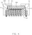
- FIG. 4is a cross-sectional view of the electrical connectorassembly of FIG. 1 ;
- FIG. 5is a top view of the electrical connector of the electrical connector assembly of FIG. 1 ;
- FIG. 6is an enlarged perspective view of a portion of the electrical connector assembly of FIG. 2 .
- an electrical connector 100includes an insulative housing 1 with a planar base (not labeled) defining an upper surface 11 and a lower surface 12 opposite to each other.
- Four L-shaped restriction parts 110are formed at four corners of the base to cooperate with the base for commonly forming a receiving cavity 10 above the upper surface 11 to receive the electronic package 200 .
- a plurality of first passageways 13are formed in the base, and two rows of second passageways 14 are formed in the base and by two sides of the first passageways 13 .
- a plurality of first contacts 2are retained in the corresponding first passageways 13 , respectively.
- Each of the first contacts 2includes a first contacting section 21 extending upwardly into the receiving cavity 10 to upwardly abut against the corresponding first pad 201 on the undersurface of the electronic package 200 .
- Each of the second contacts 3includes a second contacting section 31 upwardly extending above the upper surface 11 and sidewardly into the receiving cavity 10 to sidewardly abut against the corresponding second pad on the side face of the electronic package 200 . Therefore, the first contacts 2 provide the upward reaction forces, and the second contacts 3 provide the sideward reaction forces wherein the sum of the upward reaction force is accumulated while the sideward reaction forces are counterbalanced. Understandably, the electronic package 200 is downwardly pressed by the heat sink (not shown) when assembly.
- the sum of the frictions forces due to engagement between the second contacting sections 31 and the corresponding pads 202is smaller than that of the upward reaction forces derived from the first contacting sections 21 so that the electronic package 200 will be automatically upwardly raised up away from the receiving cavity once the heat sink is unloaded from the electrical package 200 .
- the four restriction parts 110restrain the horizontal movement of the electronic package 200 with regard to the housing 1 in both the longitudinal direction and the transverse direction perpendicular to each other wherein the housing 1 is rectangular with a pair of long sides extending the longitudinal direction and a pair of short sides extending in the transverse direction.
- the second contacting sections 31 of each row of the second contacts 3are located and exposed in the corresponding space between the corresponding restriction parts 110 at the long side so as to obtain the better heat dissipation.
- the space formed at the short sideis used for the user' finger to extend therethrough during loading or unloading the electronic package 200 with regard to the connector 100 .
- the first contact 2includes a first body 20 retained in the corresponding first passageway 13 , from which the first contacting section 21 upwardly extends for mating with the first pad 201 of the electronic package 200 , and a first soldering section 22 downwardly extends with a solder ball thereon for mounting to a printed circuit board (not shown).
- the second contact 3includes a second body 30 retained in the corresponding second passageway 14 , from which the second contacting section 31 upwardly extends for mating with the second pad 202 of the electronic package 200 , and a second soldering section 32 downwardly extends with a solder ball thereon for mounting to the same aforementioned printed circuit board.
- the first contact 2further includes a first connecting section 23 for linking to the corresponding first contact carrier strip (not shown) for assembling the first contact 2 into the corresponding first passageway 13 .
- the second contact 3further includes a second connecting section 33 for linking to the corresponding second carrier strip (not shown) for assembling the second contact 3 into the corresponding second passageway 14 .
- the distance between the second passageway 14 on the left side and the corresponding neighboring first passageway 13is smaller than that between the second passageway 14 on the right side and the corresponding neighboring first passageway 13 .
- the area defined by the first passageways 13is offset toward the left side with regard to a centerline of the housing 1 .
- an identification chamfer(not labeled) is formed on the restriction part 110 at the front right corner of the housing 1 for assuring orientation of the electronic package 200 during loading.
- a plurality of standoffs 111are formed on the upper surface 11 corresponding the first passageways 13 , respectively, against which the undersurface of the electronic package 200 downwardly abuts during mating for prevent downward excessive deformation of the first contacting sections 21 .
- the contacting point of the first contacting section 21 or that of the second contacting section 31is higher than the standoffs 110 .
- the top face of the restriction part 110is higher than the second contacting section 31 and the top face of the electronic package 200 when the undersurface of the electronic package 200 is seated upon the standoffs 111 .
Landscapes
- Engineering & Computer Science (AREA)
- Microelectronics & Electronic Packaging (AREA)
- Connecting Device With Holders (AREA)
- Coupling Device And Connection With Printed Circuit (AREA)
- Connector Housings Or Holding Contact Members (AREA)
Abstract
Description
Claims (20)
Applications Claiming Priority (2)
| Application Number | Priority Date | Filing Date | Title |
|---|---|---|---|
| CN201910618748.0 | 2019-07-10 | ||
| CN201910618748.0ACN112217009B (en) | 2019-07-10 | 2019-07-10 | Electric connector |
Publications (2)
| Publication Number | Publication Date |
|---|---|
| US20210013647A1 US20210013647A1 (en) | 2021-01-14 |
| US11264746B2true US11264746B2 (en) | 2022-03-01 |
Family
ID=74048016
Family Applications (1)
| Application Number | Title | Priority Date | Filing Date |
|---|---|---|---|
| US16/926,615ActiveUS11264746B2 (en) | 2019-07-10 | 2020-07-10 | Electrical connector having first and second plurality of contacts for respectively mating an undersurface and a side surface of electronic package |
Country Status (3)
| Country | Link |
|---|---|
| US (1) | US11264746B2 (en) |
| CN (1) | CN112217009B (en) |
| TW (1) | TW202105846A (en) |
Citations (26)
| Publication number | Priority date | Publication date | Assignee | Title |
|---|---|---|---|---|
| US3710303A (en)* | 1971-09-13 | 1973-01-09 | Rca Corp | Edge connector |
| US3871728A (en)* | 1973-11-30 | 1975-03-18 | Itt | Matched impedance printed circuit board connector |
| US4166667A (en)* | 1978-04-17 | 1979-09-04 | Gte Sylvania, Incorporated | Circuit board connector |
| US4358135A (en)* | 1979-11-02 | 1982-11-09 | Nippon Soken, Inc. | Connector for igniting circuit of priming device |
| US4601527A (en)* | 1985-01-18 | 1986-07-22 | E. I. Du Pont De Nemours And Company | Shielded header and cable assembly |
| US4710133A (en)* | 1986-06-19 | 1987-12-01 | Trw Inc. | Electrical connectors |
| US4778396A (en)* | 1984-02-06 | 1988-10-18 | Amp Incorporated | Electrical connector having compliant posts and improved insertion characteristics |
| US4795374A (en)* | 1987-05-04 | 1989-01-03 | Molex Incorporated | Double sided edge connector |
| US4806110A (en)* | 1986-06-19 | 1989-02-21 | Labinal Components And Systems, Inc. | Electrical connectors |
| US5004427A (en)* | 1986-06-19 | 1991-04-02 | Labinal Components And Systems, Inc. | Electrical connectors |
| US5169324A (en)* | 1986-11-18 | 1992-12-08 | Lemke Timothy A | Plug terminator having a grounding member |
| US5263870A (en)* | 1992-12-16 | 1993-11-23 | The Whitaker Corporation | Dual read-out SIMM socket for high electrical speed applications |
| US5433617A (en)* | 1993-06-04 | 1995-07-18 | Framatome Connectors International | Connector assembly for printed circuit boards |
| US5597313A (en)* | 1986-06-19 | 1997-01-28 | Labinal Components And Systems, Inc. | Electrical connectors |
| US5704794A (en)* | 1986-12-29 | 1998-01-06 | Labinal Components And Systems, Inc. | Electrical connectors |
| US5860814A (en)* | 1995-12-22 | 1999-01-19 | Fujitsu Takamisawa Component Limited | Electric connector for printed circuit board |
| US7097465B1 (en)* | 2005-10-14 | 2006-08-29 | Hon Hai Precision Ind. Co., Ltd. | High density connector with enhanced structure |
| TWM354226U (en) | 2008-09-19 | 2009-04-01 | Molex Taiwan Ltd | Conductive terminal and electrical connector |
| US20090264023A1 (en)* | 2008-04-22 | 2009-10-22 | Hon Hai Precision Ind. Co., Ltd. | High density connector having two-leveled contact interface |
| US20120202363A1 (en)* | 2011-02-02 | 2012-08-09 | Amphenol Corporation | Mezzanine connector |
| TWI405372B (en) | 2009-07-15 | 2013-08-11 | Molex Taiwan Ltd | Module connector and module connector combination |
| US8523615B2 (en)* | 2010-12-07 | 2013-09-03 | Hon Hai Precision Industry Co., Ltd. | Compression connector configured with two housing liminted contacts therebetween |
| US8636548B2 (en)* | 2010-10-08 | 2014-01-28 | Hon Hai Precision Industry Co., Ltd. | Card edge connector with improved central slot |
| US20140148022A1 (en)* | 2012-11-29 | 2014-05-29 | Samtec, Inc. | Low-profile mezzanine connector |
| US9543703B2 (en)* | 2012-07-11 | 2017-01-10 | Fci Americas Technology Llc | Electrical connector with reduced stack height |
| US9935385B2 (en)* | 2016-08-08 | 2018-04-03 | Te Connectivity Corporation | Receptacle connector with contact assembly |
Family Cites Families (5)
| Publication number | Priority date | Publication date | Assignee | Title |
|---|---|---|---|---|
| US4824383A (en)* | 1986-11-18 | 1989-04-25 | E. I. Du Pont De Nemours And Company | Terminator and corresponding receptacle for multiple electrical conductors |
| JP3328596B2 (en)* | 1999-01-22 | 2002-09-24 | 信越ポリマー株式会社 | Press-connecting connector and method of manufacturing the same |
| JP4925911B2 (en)* | 2007-05-08 | 2012-05-09 | 株式会社エンプラス | Socket for electrical parts |
| CN201397917Y (en)* | 2009-03-13 | 2010-02-03 | 富士康(昆山)电脑接插件有限公司 | Electric connector |
| CN203326198U (en)* | 2013-05-23 | 2013-12-04 | 富士康(昆山)电脑接插件有限公司 | Electric connector |
- 2019
- 2019-07-10CNCN201910618748.0Apatent/CN112217009B/enactiveActive
- 2020
- 2020-07-09TWTW109123120Apatent/TW202105846A/enunknown
- 2020-07-10USUS16/926,615patent/US11264746B2/enactiveActive
Patent Citations (27)
| Publication number | Priority date | Publication date | Assignee | Title |
|---|---|---|---|---|
| US3710303A (en)* | 1971-09-13 | 1973-01-09 | Rca Corp | Edge connector |
| US3871728A (en)* | 1973-11-30 | 1975-03-18 | Itt | Matched impedance printed circuit board connector |
| US4166667A (en)* | 1978-04-17 | 1979-09-04 | Gte Sylvania, Incorporated | Circuit board connector |
| US4358135A (en)* | 1979-11-02 | 1982-11-09 | Nippon Soken, Inc. | Connector for igniting circuit of priming device |
| US4778396A (en)* | 1984-02-06 | 1988-10-18 | Amp Incorporated | Electrical connector having compliant posts and improved insertion characteristics |
| US4601527A (en)* | 1985-01-18 | 1986-07-22 | E. I. Du Pont De Nemours And Company | Shielded header and cable assembly |
| US4710133A (en)* | 1986-06-19 | 1987-12-01 | Trw Inc. | Electrical connectors |
| US4806110A (en)* | 1986-06-19 | 1989-02-21 | Labinal Components And Systems, Inc. | Electrical connectors |
| US5004427A (en)* | 1986-06-19 | 1991-04-02 | Labinal Components And Systems, Inc. | Electrical connectors |
| US5597313A (en)* | 1986-06-19 | 1997-01-28 | Labinal Components And Systems, Inc. | Electrical connectors |
| US5169324A (en)* | 1986-11-18 | 1992-12-08 | Lemke Timothy A | Plug terminator having a grounding member |
| US5704794A (en)* | 1986-12-29 | 1998-01-06 | Labinal Components And Systems, Inc. | Electrical connectors |
| US4795374A (en)* | 1987-05-04 | 1989-01-03 | Molex Incorporated | Double sided edge connector |
| US5263870A (en)* | 1992-12-16 | 1993-11-23 | The Whitaker Corporation | Dual read-out SIMM socket for high electrical speed applications |
| US5433617A (en)* | 1993-06-04 | 1995-07-18 | Framatome Connectors International | Connector assembly for printed circuit boards |
| US5860814A (en)* | 1995-12-22 | 1999-01-19 | Fujitsu Takamisawa Component Limited | Electric connector for printed circuit board |
| US7097465B1 (en)* | 2005-10-14 | 2006-08-29 | Hon Hai Precision Ind. Co., Ltd. | High density connector with enhanced structure |
| US20090264023A1 (en)* | 2008-04-22 | 2009-10-22 | Hon Hai Precision Ind. Co., Ltd. | High density connector having two-leveled contact interface |
| TWM354226U (en) | 2008-09-19 | 2009-04-01 | Molex Taiwan Ltd | Conductive terminal and electrical connector |
| TWI405372B (en) | 2009-07-15 | 2013-08-11 | Molex Taiwan Ltd | Module connector and module connector combination |
| US8636548B2 (en)* | 2010-10-08 | 2014-01-28 | Hon Hai Precision Industry Co., Ltd. | Card edge connector with improved central slot |
| US8523615B2 (en)* | 2010-12-07 | 2013-09-03 | Hon Hai Precision Industry Co., Ltd. | Compression connector configured with two housing liminted contacts therebetween |
| US20120202363A1 (en)* | 2011-02-02 | 2012-08-09 | Amphenol Corporation | Mezzanine connector |
| US9543703B2 (en)* | 2012-07-11 | 2017-01-10 | Fci Americas Technology Llc | Electrical connector with reduced stack height |
| US9871323B2 (en)* | 2012-07-11 | 2018-01-16 | Fci Americas Technology Llc | Electrical connector with reduced stack height |
| US20140148022A1 (en)* | 2012-11-29 | 2014-05-29 | Samtec, Inc. | Low-profile mezzanine connector |
| US9935385B2 (en)* | 2016-08-08 | 2018-04-03 | Te Connectivity Corporation | Receptacle connector with contact assembly |
Also Published As
| Publication number | Publication date |
|---|---|
| CN112217009B (en) | 2024-06-18 |
| TW202105846A (en) | 2021-02-01 |
| CN112217009A (en) | 2021-01-12 |
| US20210013647A1 (en) | 2021-01-14 |
Similar Documents
| Publication | Publication Date | Title |
|---|---|---|
| US6881070B2 (en) | LGA connector and terminal thereof | |
| US6929483B2 (en) | Electrical contact having contact portion with enhanced resiliency | |
| US8888525B2 (en) | Electrical connector with dual arm contact | |
| US7435104B2 (en) | Socket assembly | |
| US20040048523A1 (en) | High elasticity contact for electrical connector and contact carrier | |
| US11381014B2 (en) | Electrical contact having two side-by-side parts with joined bottom ends thereof | |
| US10680374B2 (en) | Electrical contact | |
| US7207808B2 (en) | LGA socket connector having detachable aligning key | |
| US20110076894A1 (en) | Lower profile electrical socket configured with wafers | |
| US8366452B2 (en) | Low profile socket connector with improved contacts | |
| US20090035995A1 (en) | Electrical connector with improved housing structure | |
| CN112751226A (en) | Socket with improved structure | |
| US9214747B2 (en) | Low profile electrical connector have a FPC | |
| TWI827885B (en) | Electrical connector | |
| US9130321B2 (en) | Electrical connector having contact for either BGA or LGA package | |
| US7377792B2 (en) | LGA socket connector having housing with upward protective protrusion adjacent contact terminal | |
| US20100136834A1 (en) | Ic socket having positioning means for pick-up cap | |
| US20070197077A1 (en) | Land grid array connector with reinforcement stiffener | |
| US20190288431A1 (en) | Electrical contact of electrical connector | |
| US11264746B2 (en) | Electrical connector having first and second plurality of contacts for respectively mating an undersurface and a side surface of electronic package | |
| US10833442B2 (en) | Electrical connector with aligned contacting points between CPU and PCB | |
| US20130090013A1 (en) | Electrical connector for low profile application | |
| US20080318445A1 (en) | Electrical connector with improved housing | |
| US7057295B2 (en) | IC module assembly | |
| US7950933B1 (en) | Electrical socket having contact terminals floatably arranged therein |
Legal Events
| Date | Code | Title | Description |
|---|---|---|---|
| AS | Assignment | Owner name:FUDING PRECISION COMPONENTS (SHENZHEN) CO., LTD., CHINA Free format text:ASSIGNMENT OF ASSIGNORS INTEREST;ASSIGNORS:LIN, NAN-HUNG;HSU, SHUO-HSIU;REEL/FRAME:053183/0001 Effective date:20200629 Owner name:FOXCONN INTERCONNECT TECHNOLOGY LIMITED, CAYMAN ISLANDS Free format text:ASSIGNMENT OF ASSIGNORS INTEREST;ASSIGNORS:LIN, NAN-HUNG;HSU, SHUO-HSIU;REEL/FRAME:053183/0001 Effective date:20200629 | |
| FEPP | Fee payment procedure | Free format text:ENTITY STATUS SET TO UNDISCOUNTED (ORIGINAL EVENT CODE: BIG.); ENTITY STATUS OF PATENT OWNER: LARGE ENTITY | |
| STPP | Information on status: patent application and granting procedure in general | Free format text:DOCKETED NEW CASE - READY FOR EXAMINATION | |
| STPP | Information on status: patent application and granting procedure in general | Free format text:NON FINAL ACTION MAILED | |
| STPP | Information on status: patent application and granting procedure in general | Free format text:RESPONSE TO NON-FINAL OFFICE ACTION ENTERED AND FORWARDED TO EXAMINER | |
| STPP | Information on status: patent application and granting procedure in general | Free format text:NOTICE OF ALLOWANCE MAILED -- APPLICATION RECEIVED IN OFFICE OF PUBLICATIONS | |
| STCF | Information on status: patent grant | Free format text:PATENTED CASE | |
| MAFP | Maintenance fee payment | Free format text:PAYMENT OF MAINTENANCE FEE, 4TH YEAR, LARGE ENTITY (ORIGINAL EVENT CODE: M1551); ENTITY STATUS OF PATENT OWNER: LARGE ENTITY Year of fee payment:4 |