US11264530B2 - Light emitting diode (LED) devices with nucleation layer - Google Patents
Light emitting diode (LED) devices with nucleation layerDownload PDFInfo
- Publication number
- US11264530B2 US11264530B2US16/721,386US201916721386AUS11264530B2US 11264530 B2US11264530 B2US 11264530B2US 201916721386 AUS201916721386 AUS 201916721386AUS 11264530 B2US11264530 B2US 11264530B2
- Authority
- US
- United States
- Prior art keywords
- iii
- nitride
- layer
- features
- nucleation layer
- Prior art date
- Legal status (The legal status is an assumption and is not a legal conclusion. Google has not performed a legal analysis and makes no representation as to the accuracy of the status listed.)
- Active, expires
Links
Images


Classifications
- H01L33/007—
- H—ELECTRICITY
- H10—SEMICONDUCTOR DEVICES; ELECTRIC SOLID-STATE DEVICES NOT OTHERWISE PROVIDED FOR
- H10H—INORGANIC LIGHT-EMITTING SEMICONDUCTOR DEVICES HAVING POTENTIAL BARRIERS
- H10H20/00—Individual inorganic light-emitting semiconductor devices having potential barriers, e.g. light-emitting diodes [LED]
- H10H20/01—Manufacture or treatment
- H10H20/011—Manufacture or treatment of bodies, e.g. forming semiconductor layers
- H10H20/013—Manufacture or treatment of bodies, e.g. forming semiconductor layers having light-emitting regions comprising only Group III-V materials
- H10H20/0133—Manufacture or treatment of bodies, e.g. forming semiconductor layers having light-emitting regions comprising only Group III-V materials with a substrate not being Group III-V materials
- H10H20/01335—Manufacture or treatment of bodies, e.g. forming semiconductor layers having light-emitting regions comprising only Group III-V materials with a substrate not being Group III-V materials the light-emitting regions comprising nitride materials
- H—ELECTRICITY
- H01—ELECTRIC ELEMENTS
- H01L—SEMICONDUCTOR DEVICES NOT COVERED BY CLASS H10
- H01L21/00—Processes or apparatus adapted for the manufacture or treatment of semiconductor or solid state devices or of parts thereof
- H01L21/02—Manufacture or treatment of semiconductor devices or of parts thereof
- H01L21/02104—Forming layers
- H01L21/02365—Forming inorganic semiconducting materials on a substrate
- H01L21/02367—Substrates
- H01L21/0237—Materials
- H01L21/0242—Crystalline insulating materials
- H—ELECTRICITY
- H01—ELECTRIC ELEMENTS
- H01L—SEMICONDUCTOR DEVICES NOT COVERED BY CLASS H10
- H01L21/00—Processes or apparatus adapted for the manufacture or treatment of semiconductor or solid state devices or of parts thereof
- H01L21/02—Manufacture or treatment of semiconductor devices or of parts thereof
- H01L21/02104—Forming layers
- H01L21/02365—Forming inorganic semiconducting materials on a substrate
- H01L21/02436—Intermediate layers between substrates and deposited layers
- H01L21/02439—Materials
- H01L21/02455—Group 13/15 materials
- H01L21/02458—Nitrides
- H—ELECTRICITY
- H01—ELECTRIC ELEMENTS
- H01L—SEMICONDUCTOR DEVICES NOT COVERED BY CLASS H10
- H01L21/00—Processes or apparatus adapted for the manufacture or treatment of semiconductor or solid state devices or of parts thereof
- H01L21/02—Manufacture or treatment of semiconductor devices or of parts thereof
- H01L21/02104—Forming layers
- H01L21/02365—Forming inorganic semiconducting materials on a substrate
- H01L21/02518—Deposited layers
- H01L21/02521—Materials
- H01L21/02538—Group 13/15 materials
- H01L21/0254—Nitrides
- H—ELECTRICITY
- H01—ELECTRIC ELEMENTS
- H01L—SEMICONDUCTOR DEVICES NOT COVERED BY CLASS H10
- H01L21/00—Processes or apparatus adapted for the manufacture or treatment of semiconductor or solid state devices or of parts thereof
- H01L21/02—Manufacture or treatment of semiconductor devices or of parts thereof
- H01L21/02104—Forming layers
- H01L21/02365—Forming inorganic semiconducting materials on a substrate
- H01L21/02612—Formation types
- H01L21/02617—Deposition types
- H01L21/02636—Selective deposition, e.g. simultaneous growth of mono- and non-monocrystalline semiconductor materials
- H01L21/02639—Preparation of substrate for selective deposition
- H—ELECTRICITY
- H01—ELECTRIC ELEMENTS
- H01L—SEMICONDUCTOR DEVICES NOT COVERED BY CLASS H10
- H01L21/00—Processes or apparatus adapted for the manufacture or treatment of semiconductor or solid state devices or of parts thereof
- H01L21/02—Manufacture or treatment of semiconductor devices or of parts thereof
- H01L21/02104—Forming layers
- H01L21/02365—Forming inorganic semiconducting materials on a substrate
- H01L21/02612—Formation types
- H01L21/02617—Deposition types
- H01L21/02636—Selective deposition, e.g. simultaneous growth of mono- and non-monocrystalline semiconductor materials
- H01L21/02647—Lateral overgrowth
- H01L21/0265—Pendeoepitaxy
- H01L33/32—
- H—ELECTRICITY
- H10—SEMICONDUCTOR DEVICES; ELECTRIC SOLID-STATE DEVICES NOT OTHERWISE PROVIDED FOR
- H10H—INORGANIC LIGHT-EMITTING SEMICONDUCTOR DEVICES HAVING POTENTIAL BARRIERS
- H10H20/00—Individual inorganic light-emitting semiconductor devices having potential barriers, e.g. light-emitting diodes [LED]
- H10H20/01—Manufacture or treatment
- H10H20/011—Manufacture or treatment of bodies, e.g. forming semiconductor layers
- H10H20/013—Manufacture or treatment of bodies, e.g. forming semiconductor layers having light-emitting regions comprising only Group III-V materials
- H10H20/0137—Manufacture or treatment of bodies, e.g. forming semiconductor layers having light-emitting regions comprising only Group III-V materials the light-emitting regions comprising nitride materials
- H—ELECTRICITY
- H10—SEMICONDUCTOR DEVICES; ELECTRIC SOLID-STATE DEVICES NOT OTHERWISE PROVIDED FOR
- H10H—INORGANIC LIGHT-EMITTING SEMICONDUCTOR DEVICES HAVING POTENTIAL BARRIERS
- H10H20/00—Individual inorganic light-emitting semiconductor devices having potential barriers, e.g. light-emitting diodes [LED]
- H10H20/80—Constructional details
- H10H20/81—Bodies
- H10H20/819—Bodies characterised by their shape, e.g. curved or truncated substrates
- H—ELECTRICITY
- H10—SEMICONDUCTOR DEVICES; ELECTRIC SOLID-STATE DEVICES NOT OTHERWISE PROVIDED FOR
- H10H—INORGANIC LIGHT-EMITTING SEMICONDUCTOR DEVICES HAVING POTENTIAL BARRIERS
- H10H20/00—Individual inorganic light-emitting semiconductor devices having potential barriers, e.g. light-emitting diodes [LED]
- H10H20/80—Constructional details
- H10H20/81—Bodies
- H10H20/822—Materials of the light-emitting regions
- H10H20/824—Materials of the light-emitting regions comprising only Group III-V materials, e.g. GaP
- H10H20/825—Materials of the light-emitting regions comprising only Group III-V materials, e.g. GaP containing nitrogen, e.g. GaN
Definitions
- Embodiments of the disclosuregenerally relate to light emitting diode (LED) devices and methods of manufacturing the same. More particularly, embodiments are directed to light emitting diode devices that include a nucleation layer on a substrate prior to any patterning and methods for depositing a nucleation layer onto a substrate epitaxial growing a III-nitride layer thereon.
- LEDlight emitting diode
- a light emitting diodeis a semiconductor light source that emits visible light when current flows through it. LEDs combine a P-type semiconductor with an N-type semiconductor. LEDs commonly use a III-group compound semiconductor. A III-group compound semiconductor provides stable operation at a higher temperature than devices that use other semiconductors. The III-group compound is typically formed on a substrate formed of sapphire or silicon carbide (SiC).
- Direct light emitters based on patterned sapphire substrate (PSS) LEDssuffer from low luminance levels and broad angular emission patterns due to their inherent geometrical features (light is emitted from 5 sides of the chip, including the four side surfaces). These limitations can be mitigated by the use of side-coating materials to prevent light escaping from the sides of the chip and enforce light emission only from the top substrate surface. Side coating materials, however, significantly penalize light extraction efficiency (ExE), particularly in domeless emitters, as the side-coat increases light trapping in the die and it itself is not 100% reflective.
- ExElight extraction efficiency
- LEDlight emitting diode
- a light emitting diode (LED) devicecomprises a nucleation layer on a substrate, the nucleation layer comprising a first III-nitride material; a patterned dielectric layer on a top surface of the nucleation layer, the patterned dielectric layer comprising a plurality of features and having a plurality of spaces between the plurality of features; and a III-nitride layer on the plurality of features and on the plurality of spaces, the III-nitride layer comprising a second III-nitride material.
- the first III-nitride material and the second III-nitride materialmay independently be one or more of aluminum, gallium, and indium. In one or more embodiments, the first III-nitride material and the second III-nitride material independently comprises one or more of aluminum, gallium, and indium.
- the first III-nitride materialmay be aluminum nitride (AlN). In one or more embodiments, the first III-nitride material comprises aluminum nitride (AlN).
- the first III-nitride material and the second III-nitride materialmay be the same. In one or more embodiments, the first III-nitride material and the second III-nitride material are the same.
- the dielectric layermay have a low refractive index material having a refractive index in a range of from about 1.2 to about 2. In one or more embodiments, the dielectric layer comprises a low refractive index material having a refractive index in a range of from about 1.2 to about 2
- the dielectric layermay be one or more of silicon oxide (SiO 2 ) and silicon nitride (Si 3 N 4 ). In one or more embodiments, the dielectric layer comprises one or more of silicon oxide (SiO 2 ) and silicon nitride (Si 3 N 4 )
- the second III-nitride materialmay be gallium nitride (GaN).
- the second III-nitride materialcomprises gallium nitride (GaN)
- the nucleation layermay have a thickness in a range of from about 5 nm to about 100 nm. In one or more embodiments, the nucleation layer has a thickness in a range of from about 5 nm to about 100 nm.
- the plurality of featuresmay be holes. In one or more embodiments, the plurality of features comprises holes.
- the plurality of featuresmay protrude from a top surface of the nucleation layer and the plurality of spaces may expose a top surface of the nucleation layer. In one or more embodiments, the plurality of features protrude from a top surface of the nucleation layer and the plurality of spaces expose a top surface of the nucleation layer.
- the plurality of featuresmay have a shape selected from a hemispherical shape, a triangular pyramidal shape, a quadrangular pyramidal shape, a hexagonal pyramidal shape, a conical shape, a semi-spherical shape, or a cut-spherical shape.
- the plurality of featureshas a shape selected from a hemispherical shape, a triangular pyramidal shape, a quadrangular pyramidal shape, a hexagonal pyramidal shape, a conical shape, a semi-spherical shape, or a cut-spherical shape.
- the plurality of featuresmay have a height in a range of from about 100 nm to about 3 ⁇ m, a pitch in a range of from about 50 nm to about 5000 nm, and a width in a range of from about 5 nm to about 500 nm.
- the plurality of featureshas a height in a range of from about 100 nm to about 3 ⁇ m, a pitch in a range of from about 50 nm to about 5000 nm, and a width in a range of from about 5 nm to about 500 nm
- a method of manufacturing a light emitting diode (LED) devicecomprises: depositing a nucleation layer on a substrate, the nucleation layer comprising a first III-nitride material; depositing a dielectric layer on a top surface of the nucleation layer, the dielectric layer comprising a low refractive index dielectric material; patterning the dielectric layer to form a patterned surface having a plurality of features and a plurality of spaces between the plurality of features; and epitaxially growing a III-nitride layer on the patterned surface, the III-nitride layer comprising a second III-nitride material.
- the plurality of featuresmay protrude from a top surface of the nucleation layer and may have a height and a width and sidewalls, and the plurality of spaces may expose the top surface of the nucleation layer.
- the plurality of featuresprotrude from a top surface of the nucleation layer and have a height and a width and sidewalls, and the plurality of spaces expose the top surface of the nucleation layer.
- the III-nitride layermay grow on the exposed top surface of the nucleation layer and may not grow on the sidewalls of the plurality of features. In one or more embodiments, the III-nitride layer grows on the exposed top surface of the nucleation layer and does not grow on the sidewalls of the plurality of features
- the nucleation layer and the dielectric layermay be independently deposited by one or more of sputter deposition, atomic layer deposition (ALD), chemical vapor deposition (CVD), physical vapor deposition (PVD), plasma enhanced atomic layer deposition (PEALD), and plasma enhanced chemical vapor deposition (PECVD).
- the nucleation layer and the dielectric layerare independently deposited by one or more of sputter deposition, atomic layer deposition (ALD), chemical vapor deposition (CVD), physical vapor deposition (PVD), plasma enhanced atomic layer deposition (PEALD), and plasma enhanced chemical vapor deposition (PECVD).
- the plurality of featuresmay be holes, and the holes may expose a top surface of the nucleation layer.
- the plurality of featurescomprises holes, and the holes expose a top surface of the nucleation layer
- a light emitting diode (LED) devicecomprises: a patterned substrate comprising a substrate body, a plurality of integral features protruding from the substrate body, and a base surface defined by a plurality of voids between the plurality of integral features, the plurality of integral features having a top surface and sidewalls and a height, a pitch, and a width; a nucleation layer on a top surface of the plurality of integral features and not in the plurality of voids, the nucleation layer comprising a first III-nitride material; and a III-nitride layer on the nucleation layer, the III-nitride layer comprising a second III-nitride material.
- the first III-nitride material and the second III-nitride materialmay independently be one or more of aluminum, gallium, and indium. In one or more embodiments, the first III-nitride material and the second III-nitride material independently comprise one or more of aluminum, gallium, and indium.
- a method of manufacturing the light emitting diode (LED) device of the nineteenth embodimentcomprises depositing the nucleation layer on the substrate, the nucleation layer comprising the first III-nitride material; patterning the substrate to form nucleation layer-coated substrate posts separated by the plurality of voids; and epitaxially growing the III-nitride layer on the nucleation layer-coated substrate posts, the III-nitride layer comprising the second III-nitride material.
- FIG. 1illustrates a process flow diagram for a method according to one or more embodiments
- FIG. 2Aillustrates a cross-sectional view of a light emitting diode (LED) device according to one or more embodiments
- FIG. 2Billustrates a cross-sectional view of a light emitting diode (LED) device according to one or more embodiments
- FIG. 2Cillustrates a cross-sectional view of a light emitting diode (LED) device according to one or more embodiments
- FIG. 2Dillustrates a cross-sectional view of a light emitting diode (LED) device according to one or more embodiments
- FIGS. 3A-3Fillustrate perspective views of a light emitting diode (LED) device according to one or more embodiments
- FIG. 4Aillustrates a perspective view of a light emitting diode (LED) device according to one or more embodiments
- FIG. 4Billustrates a perspective view of a light emitting diode (LED) device according to one or more embodiments
- FIG. 5illustrates a process flow diagram for a method according to one or more embodiments
- FIG. 6Aillustrates a cross-sectional view of a light emitting diode (LED) device according to one or more embodiments
- FIG. 6Billustrates a cross-sectional view of a light emitting diode (LED) device according to one or more embodiments
- FIG. 6Cillustrates a cross-sectional view of a light emitting diode (LED) device according to one or more embodiments
- FIG. 6Dillustrates a cross-sectional view of a light emitting diode (LED) device according to one or more embodiments.
- FIG. 7illustrates a cross-section view of an exemplary LED package according to one or more embodiments.
- substraterefers to a structure, intermediate or final, having a surface, or portion of a surface, upon which a process acts.
- reference to a substrate in some embodimentsalso refers to only a portion of the substrate, unless the context clearly indicates otherwise.
- reference to depositing on a substrate according to some embodimentsincludes depositing on a bare substrate, or on a substrate with one or more films or features or materials deposited or formed thereon.
- the “substrate”means any substrate or material surface formed on a substrate upon which film processing is performed during a fabrication process.
- a substrate surface on which processing is performedincludes materials such as silicon, silicon oxide, silicon on insulator (SOI), strained silicon, amorphous silicon, doped silicon, carbon doped silicon oxides, germanium, gallium arsenide, glass, sapphire, and any other suitable materials such as metals, metal nitrides, III-nitrides (e.g., GaN, AlN, InN and alloys), metal alloys, and other conductive materials, depending on the application.
- Substratesinclude, without limitation, light emitting diode (LED) devices.
- Substrates in some embodimentsare exposed to a pretreatment process to polish, etch, reduce, oxidize, hydroxylate, anneal, UV cure, e-beam cure and/or bake the substrate surface.
- any of the film processing steps disclosedare also performed on an underlayer formed on the substrate, and the term “substrate surface” is intended to include such underlayer as the context indicates.
- the exposed surface of the newly deposited film/layerbecomes the substrate surface.
- a nucleation layercomprising a III-nitride material
- a nucleation layeris advantageously grown on a substrate before any patterning takes place. Without intending to be bound by theory, it is thought that this nucleation layer is important for subsequent growth of smooth coalesced III-nitride layers over the patterns.
- a thin III-nitride layer, a nucleation layeris formed (e.g., deposited) on a substrate prior to forming (e.g., depositing) a dielectric layer and forming the dielectric pattern features.
- the next process step of III-nitride material growth after a dielectric patterning stepcan be initiated at a high growth temperature. Initiating this step at a high growth temperature makes possible selective area deposition, i.e. the III-nitride material is deposited only on exposed areas of the nucleation layer and not on the dielectric material. Selective area deposition facilitates the use of patterned feature geometries with improved efficient light extraction properties, that would be difficult or impossible to use following a conventional growth sequence in which a nucleation layer is deposited after patterning the dielectric.
- FIG. 1depicts a flow diagram of a method 100 of manufacturing a light emitting diode (LED) device in accordance with one or more embodiments of the present disclosure.
- the methodbegins at operation 102 by depositing a nucleation layer on a substrate.
- a dielectric layeris deposited on the nucleation layer.
- a patterned surfaceis formed.
- a III-nitride layeris grown, e.g. epitaxially, on the areas of the nucleation layer which are not covered by dielectric material.
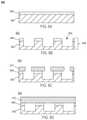
- FIG. 2Ais cross-section view of a LED device according to one or more embodiments.
- a nucleation layer 204is deposited on a substrate 202 .
- the substratemay be any substrate known to one of skill in the art.
- the substratecomprises one or more of sapphire, silicon carbide, silicon (Si), quartz, magnesium oxide (MgO), zinc oxide (ZnO), spinel, and the like.
- the substrateis not patterned prior to deposition of the nucleation layer.
- the substrateis not patterned and can be considered to be flat or substantially flat. Accordingly, in one or more embodiments, the method of the disclosure differs significantly from the conventional patterned substrate, e.g. patterned sapphire substrate (PSS), fabrication approach in which pattern features are etched directly into the substrate before deposition of a nucleation layer.
- PSSpatterned sapphire substrate
- the deposition of a nucleation layer 204 on the substrate 202 prior to patterningprovides critical advantages.
- the deposition of a nucleation layer 204 on the substrate 202 prior to patterningprovided performance improvements for directional emitters with the growth substrate remaining attached in the finished device.
- the performance improvementsinclude increased light extraction efficiency (ExE) in emitters without a lens (dome), increased brightness, and increased angular directionality (forward gain, effective increased lumen output within a narrow angular emission cone (e.g. 45 degrees).
- the nucleation layer 204comprises a III-nitride material.
- the III-nitride materialcomprises one or more of gallium (Ga), aluminum (Al), and indium (In).
- the nucleation layer 204comprises one or more of gallium nitride (GaN), aluminum nitride (AlN), indium nitride (InN), gallium aluminum nitride (GaAlN), gallium indium nitride (GaInN), aluminum gallium nitride (AlGaN), aluminum indium nitride (AlInN), indium gallium nitride (InGaN), indium aluminum nitride (InAlN), and the like.
- the nucleation layer 204comprises aluminum nitride (AlN).
- the nucleation layer 204has a thickness in a range of from about 5 nm to about 100 nm, including a range of from about 10 nm to 75 nm, a range of from about 5 nm to about 90 nm, a range of from about 10 nm to about 60 nm, a range of from about 5 nm to about 50 nm, a range of from about 10 nm to about 50 nm, and a range of from about 10 nm to about 90 nm.
- the nucleation layer 204is deposited by one or more of sputter deposition, atomic layer deposition (ALD), chemical vapor deposition (CVD), physical vapor deposition (PVD), plasma enhanced atomic layer deposition (PEALD), and plasma enhanced chemical vapor deposition (PECVD).
- ALDatomic layer deposition
- CVDchemical vapor deposition
- PVDphysical vapor deposition
- PEALDplasma enhanced atomic layer deposition
- PECVDplasma enhanced chemical vapor deposition
- Sputter depositionrefers to a physical vapor deposition (PVD) method of thin film deposition by sputtering.
- PVDphysical vapor deposition
- a materiale.g. a III-nitride
- the techniqueis based on ion bombardment of a source material, the target. Ion bombardment results in a vapor due to a purely physical process, i.e., the sputtering of the target material.
- atomic layer depositionor “cyclical deposition” refers to a vapor phase technique used to deposit thin films on a substrate surface.
- ALDatomic layer deposition
- cyclical depositionrefers to a vapor phase technique used to deposit thin films on a substrate surface.
- the process of ALDinvolves the surface of a substrate, or a portion of substrate, being exposed to alternating precursors, i.e. two or more reactive compounds, to deposit a layer of material on the substrate surface.
- the precursorsare introduced sequentially or simultaneously.
- the precursorsare introduced into a reaction zone of a processing chamber, and the substrate, or portion of the substrate, is exposed separately to the precursors.
- chemical vapor depositionrefers to a process in which films of materials are deposited from the vapor phase by decomposition of chemicals on a substrate surface.
- a substrate surfaceis exposed to precursors and/or co-reagents simultaneous or substantially simultaneously.
- substantially simultaneouslyrefers to either co-flow or where there is overlap for a majority of exposures of the precursors.
- PEALDplasma enhanced atomic layer deposition
- a materialmay be formed from the same chemical precursors, but at a higher deposition rate and a lower temperature.
- a PEALD processin general, a reactant gas and a reactant plasma are sequentially introduced into a process chamber having a substrate in the chamber. The first reactant gas is pulsed in the process chamber and is adsorbed onto the substrate surface. Thereafter, the reactant plasma is pulsed into the process chamber and reacts with the first reactant gas to form a deposition material, e.g. a thin film on a substrate.
- a purge stepmaybe conducted between the delivery of each of the reactants.
- plasma enhanced chemical vapor depositionrefers to a technique for depositing thin films on a substrate.
- a source materialwhich is in gas or liquid phase, such as a gas-phase III-nitride material or a vapor of a liquid-phase III-nitride material that have been entrained in a carrier gas, is introduced into a PECVD chamber.
- a plasma-initiated gasis also introduced into the chamber.
- the creation of plasma in the chambercreates excited radicals.
- the excited radicalsare chemically bound to the surface of a substrate positioned in the chamber, forming the desired film thereon.
- FIG. 2Bis cross-section view of a LED device according to one or more embodiments.
- a dielectric layer 206is deposited on the nucleation layer 204 .
- the term “dielectric”refers to an electrical insulator material that can be polarized by an applied electric field.
- the dielectric layerincludes, but is not limited to, oxides, e.g., silicon oxide (SiO 2 ), aluminum oxide (Al 2 O 3 ), nitrides, e.g., silicon nitride (Si 3 N 4 ).
- the dielectric layercomprises silicon nitride (Si 3 N 4 ).
- the dielectric layercomprises silicon oxide (SiO 2 ).
- the dielectric layer compositionis non-stoichiometric relative to the ideal molecular formula.
- the dielectric layerincludes, but is not limited to, oxides (e.g., silicon oxide, aluminum oxide), nitrides (e.g., silicon nitride (SiN)), oxycarbides (e.g. silicon oxycarbide (SiOC)), and oxynitrocarbides (e.g. silicon oxycarbonitride (SiNCO)).
- oxidese.g., silicon oxide, aluminum oxide
- nitridese.g., silicon nitride (SiN)
- oxycarbidese.g. silicon oxycarbide (SiOC)
- SiNCOsilicon oxycarbonitride
- the dielectric layer 206comprises a material with a low refractive index. In one or more embodiments, the dielectric layer 206 comprising a dielectric material having a refractive index in a range of from about 1.2 to about 2.
- the dielectric layer 206is deposited by one or more of sputter deposition, atomic layer deposition (ALD), chemical vapor deposition (CVD), physical vapor deposition (PVD), plasma enhanced atomic layer deposition (PEALD), and plasma enhanced chemical vapor deposition (PECVD).
- ALDatomic layer deposition
- CVDchemical vapor deposition
- PVDphysical vapor deposition
- PEALDplasma enhanced atomic layer deposition
- PECVDplasma enhanced chemical vapor deposition
- the dielectric layer 206has a thickness in a range of from about 50 nm to about 5 ⁇ m, including from about 100 nm to about 4 ⁇ m, from about 50 nm to about 4 ⁇ m, from about 200 nm to about 3 ⁇ m.
- FIG. 2Cis cross-section view of a LED device according to one or more embodiments.
- a patterned surfaceis formed.
- a patterned dielectric layer 207is formed.
- the dielectric layer 206is patterned according to any appropriate patterning technique known to one of skill in the art.
- the patterned dielectric layer 207comprises a plurality of features 208 protruding from the top surface of the nucleation layer 204 and having a plurality of spaces 210 between the plurality of features 208 .
- the plurality of features 208 protruding from the surface of the nucleation layer 204can have any shape known to one of skill in the art.
- FIGS. 3A-3Fillustrate perspective views of a light emitting diode (LED) device according to one or more embodiments. Specifically, FIGS. 3A-3F illustrate various embodiments of the shapes of the plurality of features 208 protruding from the top surface of the nucleation layer 204 .
- LEDlight emitting diode
- the shape of the plurality of protruding features 208includes, but is not limited to, a hemispherical shape ( FIG. 3A ), a triangular pyramidal shape ( FIG. 3B ), a quadrangular pyramidal shape ( FIG. 3C ), a hexagonal pyramidal shape ( FIG. 3D ), a conical shape ( FIG. 3E ), a semi-spherical shape or a cut-spherical shape ( FIG. 3F ).
- the plurality of features 208 protruding from the surface of the nucleation layer 204has a height in a range of from about 100 nm to about 3 ⁇ m, include a range of from about 500 nm to about 2 ⁇ m, a range of from about 100 nm to about 1 ⁇ m, a range of from about 250 nm to about 2.5 ⁇ m, and a range of from about 100 nm to about 2 ⁇ m.
- the plurality of features 208 protruding from the surface of the nucleation layer 204has a pitch in a range of from about 50 nm to about 5000 nm, including a range from about 500 nm to about 2000 nm, and a range of from about 500 nm to about 1000 nm.
- the plurality of features 208 protruding from the surface of the nucleation layer 204has a width in a range of from about 5 nm to about 500 nm, including a range from about 10 nm to about 500 nm, and a range of from about 5 nm to about 300 nm.
- a hexagonal pattern of a plurality of features 208 protruding from the surface of the nucleation layer 204 having a pitch of about 1000 nm and a circle diameter of about 200 nmis transferred to a photoresist coating (not illustrated) on the dielectric layer 206 using nanoimprint lithography.
- the substrate 202is etched in a reactive ion etching (RIE) tool using conditions that etch the dielectric layer 206 efficiently but etch the nucleation layer 204 very slowly or not at all. In other words, the etching is selective to the dielectric layer 206 over the nucleation layer 204 .
- RIEreactive ion etching
- the photoresistis removed and the wafer is cleaned, resulting in a hexagonal array of cones the dielectric layer 204 .
- the half-angle of the plurality of features 208is controlled by adjusting parameters such as the thickness of the starting dielectric layer 206 , thickness of photoresist layer (not illustrated), and differences in RIE etch rates that depend on surface angles and/or materials.
- FIG. 2Dis cross-section view of a LED device according to one or more embodiments.
- a III-nitride layer 212is grown, e.g. epitaxially, on the patterned dielectric layer 207 .
- a III-nitride layeris grown on the nucleation layer 204 and in or on the plurality of spaces 210 between the plurality of features 208 , and not on the dielectric layer 206 .
- the plurality of features 208have at least one sidewall (not illustrated), and the III-nitride layer does not grow on the at least one sidewall of the plurality of features 208 .
- the III-nitride layer 212comprises a III-nitride material.
- the III-nitride materialcomprises one or more of gallium (Ga), aluminum (Al), and indium (In).
- the III-nitride layer 212comprises one or more of gallium nitride (GaN), aluminum nitride (AlN), indium nitride (InN), gallium aluminum nitride (GaAlN), gallium indium nitride (GaInN), aluminum gallium nitride (AlGaN), aluminum indium nitride (AlInN), indium gallium nitride (InGaN), indium aluminum nitride (InAlN), and the like.
- the III-nitride layer 212comprises gallium nitride. In some embodiments, the III-nitride layer 212 and the nucleation layer 204 comprise the same III-nitride material. In other embodiments, the III-nitride layer 212 and the nucleation layer 204 comprise different III-nitride materials. In a specific embodiment, the nucleation layer 204 comprises aluminum nitride (AlN) and the III-nitride layer 212 comprises gallium nitride (GaN).
- the III-nitride layer 212is placed in a metalorganic vapor-phase epitaxy (MOVPE) reactor for epitaxy of LED device layers.
- MOVPEmetalorganic vapor-phase epitaxy
- the MOVPE processstarts with high temperature III-nitride growth taking advantage of the large difference in III-nitride nucleation rates on the pre-deposited nucleation layer 204 versus the surfaces of patterned dielectric layer 207 and plurality of features 208 .
- the device 200is processed as is typical for a conventional PSS based LED.
- pre-deposition of the nucleation layer 204allows high temperature selective area growth around the plurality of features 208 , and, thus, more freedom in pattern feature geometry since nucleation of unwanted misoriented grains on the pattern features is avoided.
- the temperature at which the III-nitride layer is grownis in a range of from about 800° C. to about 1200° C., or from about 950° C. to about 1150° C.
- FIGS. 4A and 4Bare perspective views of a LED device according to one or more embodiments.
- a nucleation layer 204has been deposited on a substrate 202
- a dielectric layer 206has been deposited on the nucleation layer 204 , as described above.
- the dielectric layer 206is then patterned by any appropriate patterning technique known to one of skill in the art.
- the patterned dielectric layer 307has a plurality of features 308 .
- the plurality of features 308comprise holes 311 that extend to the nucleation layer 204 .
- the holes 311are any appropriate shape or size known to one of skill in the art.
- the plurality of features 308 or the holes 311have a diameter in a range of from about 50 nm to about 5000 nm.
- the plurality of features 308has a depth that is equal to the thickness of the dielectric layer 204 .
- the depth of the holesmay be at least equal to the thickness of the dielectric layer. In some embodiments, the depth of the holes may extend up to about 500 nm deeper than the thickness of the dielectric layer 204 .
- the holes 311are regularly spaced. In other embodiments, the holes 311 are irregularly spaced. In one or more embodiments, the plurality of features 308 (i.e. holes 311 ) have a plurality of spaces 310 between the plurality of features 308 .
- a III-nitride layer 312is grown, e.g. epitaxially, on the patterned dielectric layer 307 .
- the III-nitride layer 312fills the plurality of features 308 (i.e. holes 311 ) and comes in contact with the nucleation layer 204 .
- the III-nitride layer 312comprises a III-nitride material.
- the III-nitride materialcomprises one or more of gallium (Ga), aluminum (Al), and indium (In).
- the III-nitride layer 312comprises one or more of gallium nitride (GaN), aluminum nitride (AlN), indium nitride (InN), gallium aluminum nitride (GaAlN), gallium indium nitride (GaInN), aluminum gallium nitride (AlGaN), aluminum indium nitride (AlInN), indium gallium nitride (InGaN), indium aluminum nitride (InAlN), and the like.
- the III-nitride layer 312comprises gallium nitride. In some embodiments, the III-nitride layer 312 and the nucleation layer 204 comprise the same III-nitride material. In other embodiments, the III-nitride layer 312 and the nucleation layer 204 comprise different III-nitride materials. In a specific embodiment, the nucleation layer 204 comprises aluminum nitride (AlN) and the III-nitride layer 312 comprises gallium nitride (GaN).
- the growth method disclosed hereini.e. forming an epitaxial nucleation layer on the substrate before forming a plurality of features in the dielectric layer
- the patterned featuresare packed more densely together than would be possible with current state-of-the-art methods that utilize etching of sapphire before nucleation layer deposition because of the selective area growth around the dielectric patterns.
- FIG. 5depicts a flow diagram of a method 500 of manufacturing a light emitting diode (LED) device in accordance with one or more alternative embodiments of the present disclosure.
- the methodbegins at operation 502 by depositing a nucleation layer on a substrate.
- the substrateis patterned.
- a III-nitride layeris selectively grown, e.g. epitaxially, on the nucleation layer.
- FIG. 6Ais cross-section view of a LED device according to one or more embodiments.
- a nucleation layer 604is deposited on a substrate 602 .
- the substrate 602is any suitable substrate known to one of skill in the art, including any of the substrates described through the disclosure. In one or more specific embodiments, the substrate 602 comprises sapphire.
- the deposition of a nucleation layer 604 on the substrate 602 prior to patterningprovides critical advantages.
- the deposition of a nucleation layer 604 on the substrate 602 prior to patterningprovided performance improvements for directional emitters with the growth substrate remaining attached in the finished device.
- the performance improvementsinclude increased light extraction efficiency (ExE) in emitters without a lens (dome), increased brightness, and increased angular directionality (forward gain, effective increased lumen output within a narrow angular emission cone (e.g. 45 degrees)
- the nucleation layer 604is deposited by one or more of sputter deposition, atomic layer deposition (ALD), chemical vapor deposition (CVD), physical vapor deposition (PVD), plasma enhanced atomic layer deposition (PEALD), and plasma enhanced chemical vapor deposition (PECVD).
- ALDatomic layer deposition
- CVDchemical vapor deposition
- PVDphysical vapor deposition
- PEALDplasma enhanced atomic layer deposition
- PECVDplasma enhanced chemical vapor deposition
- the nucleation layer 604comprises a III-nitride material.
- the III-nitride materialcomprises one or more of gallium (Ga), aluminum (Al), and indium (In).
- the nucleation layer 604comprises one or more of gallium nitride (GaN), aluminum nitride (AlN), indium nitride (InN), gallium aluminum nitride (GaAlN), gallium indium nitride (GaInN), aluminum gallium nitride (AlGaN), aluminum indium nitride (AlInN), indium gallium nitride (InGaN), indium aluminum nitride (InAlN), and the like.
- the nucleation layer 604comprises aluminum nitride (AlN).
- the nucleation layer 604has a thickness in a range of from about 5 nm to about 100 nm, including a range of from about 10 nm to 75 nm, a range of from about 5 nm to about 90 nm, a range of from about 10 nm to about 60 nm, a range of from about 5 nm to about 50 nm, a range of from about 10 nm to about 50 nm, and a range of from about 10 nm to about 90 nm.
- FIG. 6Bis cross-section view of a LED device according to one or more embodiments.
- the substrate 602 and nucleation layer 604are patterned to form voids 605 .
- the voids 605have any shape known to the skilled artisan, including, but not limited to, rectangular, triangular, oval, rounded, hexagonal, and the like.
- the plurality of voids 605may have a thickness approximately determined by the depth of the substrate etch step. In one or more embodiments, the depth of the plurality of voids 605 may be in a range of from about 50 nm to about 5000 nm.
- the plurality of voids 605has a pitch in a range of from about 50 nm to about 5000 nm, including a range from about 500 nm to about 2000 nm, and a range of from about 500 nm to about 1000 nm.
- the plurality of voidshas a width in a range of from about 5 nm to about 500 nm, including a range from about 10 nm to about 500 nm, and a range of from about 5 nm to about 300 nm.
- a hexagonal pattern of voids 605is transferred to a photoresist coating (not illustrated) on the nucleation layer 204 using conventional photolithography.
- the device 600is etched to a depth in an RIE tool using conditions that efficiently etch both the nucleation layer 204 and the substrate 202 , resulting in a void having substantially vertical sidewall angles.
- the resultis an array of nucleation layer-coated substrate posts 609 .
- FIG. 6Cis cross-section view of a LED device according to one or more embodiments.
- a III-nitride layer 612is grown, e.g. epitaxially, on the nucleation layer-coated substrate posts 609 .
- FIG. 6Dis cross-section view of a LED device according to one or more embodiments. With reference to FIG. 6D , the III-nitride layer 612 is grown, e.g. epitaxially, laterally on the nucleation layer-coated substrate posts 609 .
- the III-nitride layer 612comprises a III-nitride material.
- the III-nitride materialcomprises one or more of gallium (Ga), aluminum (Al), and indium (In).
- the III-nitride layer 212comprises one or more of gallium nitride (GaN), aluminum nitride (AlN), indium nitride (InN), gallium aluminum nitride (GaAlN), gallium indium nitride (GaInN), aluminum gallium nitride (AlGaN), aluminum indium nitride (AlInN), indium gallium nitride (InGaN), indium aluminum nitride (InAlN), and the like.
- the III-nitride layer 612comprises gallium nitride. In some embodiments, the III-nitride layer 612 and the nucleation layer 204 comprise the same III-nitride material. In other embodiments, the III-nitride layer 612 and the nucleation layer 204 comprise different III-nitride materials. In a specific embodiment, the nucleation layer 204 comprises aluminum nitride (AlN) and the III-nitride layer 612 comprises gallium nitride (GaN).
- the device 600is loaded into a MOVPE reactor for epitaxy of LED device layers. Unlike during a typical MOVPE growth run, which starts with a low temperature nucleation layer, in one or more embodiments the MOVPE process starts with high temperature III-nitride growth taking advantage of the large difference in III-nitride nucleation rates on the pre-deposited nucleation layer 204 versus the etched substrate 202 surfaces not covered by the nucleation layer 204 . In one or more embodiments, the III-nitride layer grows laterally and coalesces above the voids 605 in the substrate 202 leaving an array of buried void features.
- the voids 605have a refractive index equal to 1, as the voids are filled with air. In one or more embodiments, after the MOVPE growth run, subsequent processing of the device 600 follows as usual for a conventional PSS based LED.
- performance improvements of the LED device of one or more embodimentsare, in part, a consequence of fabricating the plurality of features from a material with lower refractive index, e.g. low refractive index dielectric material or voids (air), than a substrate, such as a sapphire substrate.
- the low refractive index features 208 or voids 605produce a narrow beam angular profile, which is significantly lower than that produced by state-of the art patterned sapphire substrate (PSS), even in side-coated architectures.
- the narrowing levelis quantified by defining a forward-gain parameter (fwdGain).
- the fwdGainmay be defined with respect to different cone angles, e.g. 5 deg, 45 deg and 60 deg, and helps establish the relative level of light concentration within a given cone angle centered at normal. The higher the fwdGain is, the higher the concentration of light.
- PSS LED emitters with side-coatinghave a fwdGain (45) ⁇ 0.5, with a full width half max (FWHM) >120 deg.
- the product of fwdGain and light extraction efficiency (ExE)allows quantifying the relative flux gains concentrated within a given angular acceptance cone.
- the LED device of one of more embodimentsis useful in any product known to one of skill in the art which uses a side-coated chip-scale package (CSP) architecture.
- the term “chip-scale package (CSP)”refers to a type of integrated circuit package.
- a chip-scale packageis provided which has an area no greater than about 1.2 times that of the die, which is a single-die, direct surface mountable package.
- the CSPhas a ball pitch that is less than or equal to about 1 mm.
- FIG. 7is a cross-section view of an exemplary LED package 700 according to one or more embodiments. Referring to FIG. 7 , a chip-scale package (CSP) LED unit 700 comprising the LED device 702 of one or more embodiments. An anode 704 and a cathode 706 are soldered to the LED device 702 .
- a nucleation layer of AlNwas deposited on a non-patterned sapphire substrate using a sputter deposition tool.
- a SiO 2 layer of thickness 800 nmwas coated over the AlN layer using plasma-enhanced chemical vapor deposition (PECVD).
- PECVDplasma-enhanced chemical vapor deposition
- a hexagonal pattern of circles having a pitch of 1000 nm and a circle diameter of 200 nmwas transferred to a photoresist coating on the SiO 2 layer using nanoimprint lithography.
- the waferwas etched in an reactive ion etching (RIE) tool using conditions that etch SiO 2 efficiently but etch AlN very slowly or not at all. After the photoresist was removed and the wafer cleaned, the result was a hexagonal array of cones of SiO 2 .
- RIEreactive ion etching
- the half-angle of the coneswas about 35 degrees and was controlled by adjusting parameters such as the thickness of the starting SiO 2 layer, thickness of photoresist layer, and differences in RIE etch rates that depend on surface angles and/or materials.
- the waferwas then loaded into a III-nitride MOVPE reactor for epitaxy of LED device layers. Unlike a typical MOVPE growth run which starts with a low temperature nucleation layer, the MOVPE process in this case started with high temperature GaN growth taking advantage of the large difference in GaN nucleation rates on the predeposited AlN vs. the surfaces of the SiO 2 cone features. After the MOVPE growth run. Subsequent processing of the wafer followed as usual for a conventional PSS based LED.
- a nucleation layer of AlNwas deposited on a non-patterned sapphire substrate using a sputter deposition tool.
- a hexagonal pattern of voids having a pitch of 2000 nm and a void diameter of 750 nmwas transferred to a photoresist coating on the AlN layer using conventional photolithography.
- the waferwas etched to a depth of 600 nm in an RIE tool using conditions that efficiently etch both AlN and sapphire resulting in a nearly vertical sidewall angle. After removing the photoresist and cleaning the wafer the result was an array of AlN-coated sapphire posts.
- the waferwas then loaded into a III-nitride MOVPE reactor for epitaxy of LED device layers.
- the MOVPE processin this case started with high temperature GaN growth taking advantage of the large difference in GaN nucleation rates on the pre-deposited AlN vs. the etched sapphire surfaces not covered by AlN.
- subsequent processing of the waferfollows as usual for a conventional PSS based LED.
Landscapes
- Engineering & Computer Science (AREA)
- Physics & Mathematics (AREA)
- Condensed Matter Physics & Semiconductors (AREA)
- General Physics & Mathematics (AREA)
- Manufacturing & Machinery (AREA)
- Computer Hardware Design (AREA)
- Microelectronics & Electronic Packaging (AREA)
- Power Engineering (AREA)
- Chemical & Material Sciences (AREA)
- Crystallography & Structural Chemistry (AREA)
- Materials Engineering (AREA)
- Led Devices (AREA)
Abstract
Description
Claims (13)
Priority Applications (3)
| Application Number | Priority Date | Filing Date | Title |
|---|---|---|---|
| US16/721,386US11264530B2 (en) | 2019-12-19 | 2019-12-19 | Light emitting diode (LED) devices with nucleation layer |
| US17/531,922US20220085236A1 (en) | 2019-12-19 | 2021-11-22 | Light Emitting Diode (LED) Devices With Nucleation Layer |
| US17/570,605US12408481B2 (en) | 2019-12-19 | 2022-01-07 | Light emitting diode (LED) devices with nucleation layer |
Applications Claiming Priority (1)
| Application Number | Priority Date | Filing Date | Title |
|---|---|---|---|
| US16/721,386US11264530B2 (en) | 2019-12-19 | 2019-12-19 | Light emitting diode (LED) devices with nucleation layer |
Related Child Applications (2)
| Application Number | Title | Priority Date | Filing Date |
|---|---|---|---|
| US17/531,922DivisionUS20220085236A1 (en) | 2019-12-19 | 2021-11-22 | Light Emitting Diode (LED) Devices With Nucleation Layer |
| US17/570,605Continuation-In-PartUS12408481B2 (en) | 2019-12-19 | 2022-01-07 | Light emitting diode (LED) devices with nucleation layer |
Publications (2)
| Publication Number | Publication Date |
|---|---|
| US20210193863A1 US20210193863A1 (en) | 2021-06-24 |
| US11264530B2true US11264530B2 (en) | 2022-03-01 |
Family
ID=76438756
Family Applications (2)
| Application Number | Title | Priority Date | Filing Date |
|---|---|---|---|
| US16/721,386Active2040-02-15US11264530B2 (en) | 2019-12-19 | 2019-12-19 | Light emitting diode (LED) devices with nucleation layer |
| US17/531,922AbandonedUS20220085236A1 (en) | 2019-12-19 | 2021-11-22 | Light Emitting Diode (LED) Devices With Nucleation Layer |
Family Applications After (1)
| Application Number | Title | Priority Date | Filing Date |
|---|---|---|---|
| US17/531,922AbandonedUS20220085236A1 (en) | 2019-12-19 | 2021-11-22 | Light Emitting Diode (LED) Devices With Nucleation Layer |
Country Status (1)
| Country | Link |
|---|---|
| US (2) | US11264530B2 (en) |
Cited By (1)
| Publication number | Priority date | Publication date | Assignee | Title |
|---|---|---|---|---|
| WO2024129716A1 (en) | 2022-12-15 | 2024-06-20 | Lumileds Llc | Microleds with nanopatterned surface |
Families Citing this family (5)
| Publication number | Priority date | Publication date | Assignee | Title |
|---|---|---|---|---|
| US20230154968A1 (en)* | 2021-11-12 | 2023-05-18 | Lumileds Llc | Thin-film led array with low refractive index patterned structures |
| US20230155070A1 (en)* | 2021-11-12 | 2023-05-18 | Lumileds Llc | Thin-film led array with low refractive index patterned structures and reflector |
| WO2023137714A1 (en)* | 2022-01-21 | 2023-07-27 | 佛山市柔浩电子有限公司 | Micro led chip, preparation method therefor, and eutectic structure containing same |
| WO2023137713A1 (en)* | 2022-01-21 | 2023-07-27 | 佛山市柔浩电子有限公司 | Micro led chip detection structure and preparation method therefor |
| CN115692570B (en)* | 2022-08-24 | 2025-07-11 | 聚灿光电科技股份有限公司 | An LED chip based on an aluminum oxide silicon oxide composite substrate and a manufacturing method thereof |
Citations (67)
| Publication number | Priority date | Publication date | Assignee | Title |
|---|---|---|---|---|
| US5283447A (en) | 1992-01-21 | 1994-02-01 | Bandgap Technology Corporation | Integration of transistors with vertical cavity surface emitting lasers |
| US5413967A (en) | 1991-05-16 | 1995-05-09 | Kabushiki Kaisha Toshiba | Method of manufacturing semiconductor devices |
| US5952681A (en) | 1997-11-24 | 1999-09-14 | Chen; Hsing | Light emitting diode emitting red, green and blue light |
| JP2002324915A (en) | 2001-04-24 | 2002-11-08 | Nichia Chem Ind Ltd | Integrated nitride semiconductor light emitting device |
| US20020187568A1 (en) | 2001-06-11 | 2002-12-12 | Stockman Stephen A. | Forming semiconductor structures including acticated acceptors in buried p-type gan layers |
| WO2005073485A2 (en) | 2004-01-29 | 2005-08-11 | Rwe Space Solar Power Gmbh | Semiconductor structure comprising active zones |
| JP2005236667A (en) | 2004-02-19 | 2005-09-02 | Nippon Telegr & Teleph Corp <Ntt> | Communications system |
| US20060060866A1 (en) | 2000-03-14 | 2006-03-23 | Toyoda Gosel Co., Ltd. | Group III nitride compound semiconductor devices and method for fabricating the same |
| US20070170444A1 (en) | 2004-07-07 | 2007-07-26 | Cao Group, Inc. | Integrated LED Chip to Emit Multiple Colors and Method of Manufacturing the Same |
| US20080251799A1 (en) | 2007-04-13 | 2008-10-16 | Kabushiki Kaisha Toshiba | Light emitting device |
| US20090078955A1 (en) | 2007-09-26 | 2009-03-26 | Iii-N Technlogy, Inc | Micro-Emitter Array Based Full-Color Micro-Display |
| US20090090932A1 (en) | 2006-09-06 | 2009-04-09 | Palo Alto Research Incorporated | Nitride semiconductor ultraviolet leds with tunnel junctions and reflective contact |
| US20100117997A1 (en) | 2007-03-08 | 2010-05-13 | Haase Michael A | Array of luminescent elements |
| US20110012109A1 (en) | 2009-07-17 | 2011-01-20 | Applied Materials, Inc. | Method of forming a group iii-nitride crystalline film on a patterned substrate by hydride vapor phase epitaxy (hvpe) |
| US20110027925A1 (en) | 2009-07-28 | 2011-02-03 | Canon Kabushiki Kaisha | Surface emitting laser, method for producing surface emitting laser, and image forming apparatus |
| US20110163223A1 (en) | 2006-10-05 | 2011-07-07 | Guidash Robert M | Active pixel sensor having two wafers |
| US8022421B2 (en) | 2007-11-06 | 2011-09-20 | Industrial Technology Institute | Light emitting module having LED pixels and method of forming the same |
| DE102010002966A1 (en) | 2010-03-17 | 2011-09-22 | Osram Opto Semiconductors Gmbh | A laser diode array and method of making a laser diode array |
| US20110233575A1 (en) | 2010-03-26 | 2011-09-29 | Taiwan Semiconductor Manufacturing Company, Ltd. | Single phosphor layer photonic device for generating white light or color lights |
| US20110256648A1 (en) | 2008-12-24 | 2011-10-20 | 3M Innovative Properties Company | Method of Making Double-sided Wavelength Converter and Light Generating Device Using Same |
| US8114691B2 (en) | 2004-12-08 | 2012-02-14 | Samsung Led Co., Ltd. | Semiconductor light emitting device having textured structure and method of manufacturing the same |
| US20120135557A1 (en) | 2010-11-25 | 2012-05-31 | Toyoda Gosei Co., Ltd. | Group iii nitride semiconductor light-emitting device |
| WO2012077884A1 (en) | 2010-12-10 | 2012-06-14 | Chung Hoon Lee | Method of fabricating semiconductor device using gang bonding and semiconductor device fabricated by the same |
| US20120276722A1 (en) | 2011-04-27 | 2012-11-01 | Jen-Inn Chyi | Method for growing semipolar nitride |
| US20130022063A1 (en) | 2011-07-22 | 2013-01-24 | Fuji Xerox Co., Ltd. | Vertical-cavity surface-emitting laser array, vertical-cavity surface-emitting laser device, optical transmission apparatus, and information processing apparatus |
| US20130069191A1 (en) | 2010-10-13 | 2013-03-21 | Zvi Or-Bach | Novel semiconductor and optoelectronic devices |
| US20130193308A1 (en) | 2011-12-21 | 2013-08-01 | Arizona State | Multiband Photodetector Utilizing Unipolar and Bipolar Devices |
| US20130193448A1 (en) | 2012-01-30 | 2013-08-01 | Lextar Electronics Corporation | Patterned substrate and stacked light emitting diode |
| US20130252361A1 (en)* | 2006-10-19 | 2013-09-26 | Taiwan Semiconductor Manufacturing Company, Ltd. | Light-Emitter-Based Devices with Lattice-Mismatched Semiconductor Structures |
| EP2743966A1 (en) | 2012-12-14 | 2014-06-18 | Seoul Viosys Co., Ltd. | Epitaxial layer wafer having void for separating growth substrate therefrom and semiconductor device fabricated using the same |
| US20140191243A1 (en) | 2013-01-08 | 2014-07-10 | University Of Florida Research Foundation, Inc. | Patterned articles and light emitting devices therefrom |
| US20150024524A1 (en) | 2012-03-05 | 2015-01-22 | Enraytek Optoelectronics Co., Ltd | Methods for Manufacturing Isolated Deep Trench and High-Voltage LED Chip |
| US20150093847A1 (en)* | 2012-04-19 | 2015-04-02 | Hunetplus Co., Ltd. | Method for fabricating nano-patterned substrate for high-efficiency nitride-based light-emitting diode |
| US20150093121A1 (en) | 2013-10-02 | 2015-04-02 | Fujitsu Limited | Optical semiconductor device, optical semiconductor device array, and optical transmitter module |
| US20150115290A1 (en) | 2012-06-22 | 2015-04-30 | Soitec | Method of manufacturing structures of leds or solar cells |
| US20150270434A1 (en) | 2012-09-27 | 2015-09-24 | Osram Opto Semiconductors Gmbh | Optoelectronic device and method for producing an optoelectronic device |
| US20160197151A1 (en) | 2014-12-01 | 2016-07-07 | Yale University | Method to make buried, highly conductive p-type iii-nitride layers |
| US9537050B2 (en) | 2013-05-14 | 2017-01-03 | Commissariat A L'energie Atomique Et Aux Energies Alternatives | Optoelectronic device and method for manufacturing same |
| US20170025567A1 (en) | 2015-07-24 | 2017-01-26 | Epistar Corporation | Light-emitting device and manufacturing method thereof |
| US20170098746A1 (en) | 2015-10-01 | 2017-04-06 | Cree, Inc. | Low optical loss flip chip solid state lighting device |
| WO2017067333A1 (en) | 2015-10-23 | 2017-04-27 | 厦门市三安光电科技有限公司 | Patterned substrate, preparation method, and a light-emitting diode |
| US20170181241A1 (en) | 2015-10-02 | 2017-06-22 | Samsung Electronics Co., Ltd. | White Light Emitting Module and LED Lighting Apparatus |
| US20170213868A1 (en) | 2014-04-01 | 2017-07-27 | Centre National De La Recherche Scientifique | Semiconducting pixel, matrix of such pixels, semiconducting structure for the production of such pixels and their methods of fabrication |
| CN107068811A (en) | 2017-03-15 | 2017-08-18 | 京东方科技集团股份有限公司 | The preparation method and light-emitting diode assembly of light-emitting diode assembly |
| US20170323788A1 (en) | 2016-05-09 | 2017-11-09 | Regents Of The University Of Michigan | Metal based nanowire tunnel junctions |
| US20170338373A1 (en) | 2016-05-20 | 2017-11-23 | Lumileds Llc | Method of forming a p-type layer for a light emitting device |
| KR20170129009A (en) | 2016-05-16 | 2017-11-24 | 엘지이노텍 주식회사 | Semiconductor device |
| JP6245319B1 (en) | 2016-06-30 | 2017-12-13 | 富士ゼロックス株式会社 | Light emitting component, print head, image forming apparatus, and semiconductor multilayer substrate |
| US20180019359A1 (en) | 2009-10-23 | 2018-01-18 | Alta Devices, Inc. | Multi-junction optoelectronic device |
| US9876141B2 (en) | 2013-06-19 | 2018-01-23 | Koninklijke Philips N.V. | LED with patterned surface features based on emission field patterns |
| US20180104130A1 (en) | 2016-10-19 | 2018-04-19 | Dynatronics Corporation | System and methods for providing and using a knee range of motion device |
| US10002928B1 (en) | 2014-12-23 | 2018-06-19 | Soraa Laser Diode, Inc. | Manufacturable RGB display based on thin film gallium and nitrogen containing light emitting diodes |
| US20180182919A1 (en) | 2016-12-28 | 2018-06-28 | Toyoda Gosei Co., Ltd. | Semiconductor Structure and Semiconductor Device |
| US10050080B2 (en) | 2013-05-14 | 2018-08-14 | Commissariat A L'energie Atomique Et Aux Energies Alternatives | Optoelectronic device and method for manufacturing same |
| US20180269532A1 (en) | 2015-10-23 | 2018-09-20 | Seiko Epson Corporation | Manufacturing method of electrode assembly |
| US10090437B2 (en) | 2013-02-11 | 2018-10-02 | Lumileds Llc | LED having etched light emitting surface for increased light extraction |
| US20190006178A1 (en)* | 2017-06-29 | 2019-01-03 | Globalwafers Co., Ltd. | Semiconductor device and method of forming the same |
| US20190006821A1 (en) | 2017-06-29 | 2019-01-03 | Silanna UV Technologies Pte Ltd | Transverse mode-confined deep-uv led |
| US20190074404A1 (en) | 2015-07-10 | 2019-03-07 | The Regents Of The University Of California | Hybrid growth method for iii-nitride tunnel junction devices |
| US10249800B1 (en) | 2017-10-03 | 2019-04-02 | Lockheed Martin Corporation | Stacked transparent pixel structures for electronic displays |
| US20190148586A1 (en) | 2016-03-29 | 2019-05-16 | Enkris Semiconductor, Inc | Patterned si substrate-based led epitaxial wafer and preparation method therefor |
| US20190198561A1 (en) | 2017-12-22 | 2019-06-27 | Lumileds Llc | Iii-nitride multi-wavelength led for visible light communication enabled by tunnel junctions |
| US10355168B2 (en) | 2014-05-30 | 2019-07-16 | Lumileds Llc | Light-emitting device with patterned substrate |
| US20190229234A1 (en) | 2016-10-08 | 2019-07-25 | Goertek. Inc | Display device and electronics apparatus |
| US20190279558A1 (en) | 2018-03-09 | 2019-09-12 | Lumileds Holding B.V. | Passive matrix led display assembly |
| US20200194549A1 (en)* | 2017-09-29 | 2020-06-18 | Intel Corporation | Multi-step lateral epitaxial overgrowth for low defect density iii-n films |
| US20210118680A1 (en)* | 2019-10-22 | 2021-04-22 | Imec Vzw | Method for Manufacturing an III-Nitride Semiconductor Structure |
- 2019
- 2019-12-19USUS16/721,386patent/US11264530B2/enactiveActive
- 2021
- 2021-11-22USUS17/531,922patent/US20220085236A1/ennot_activeAbandoned
Patent Citations (83)
| Publication number | Priority date | Publication date | Assignee | Title |
|---|---|---|---|---|
| US5413967A (en) | 1991-05-16 | 1995-05-09 | Kabushiki Kaisha Toshiba | Method of manufacturing semiconductor devices |
| US5283447A (en) | 1992-01-21 | 1994-02-01 | Bandgap Technology Corporation | Integration of transistors with vertical cavity surface emitting lasers |
| US5952681A (en) | 1997-11-24 | 1999-09-14 | Chen; Hsing | Light emitting diode emitting red, green and blue light |
| US20060060866A1 (en) | 2000-03-14 | 2006-03-23 | Toyoda Gosel Co., Ltd. | Group III nitride compound semiconductor devices and method for fabricating the same |
| JP2002324915A (en) | 2001-04-24 | 2002-11-08 | Nichia Chem Ind Ltd | Integrated nitride semiconductor light emitting device |
| US20020187568A1 (en) | 2001-06-11 | 2002-12-12 | Stockman Stephen A. | Forming semiconductor structures including acticated acceptors in buried p-type gan layers |
| US7692202B2 (en) | 2004-01-29 | 2010-04-06 | Azur Space Solar Power Gmbh | Semiconductor structure comprising active zones |
| WO2005073485A2 (en) | 2004-01-29 | 2005-08-11 | Rwe Space Solar Power Gmbh | Semiconductor structure comprising active zones |
| US20070158659A1 (en) | 2004-01-29 | 2007-07-12 | Rwe Space Solar Power Gmbh | Semiconductor Structure Comprising Active Zones |
| JP2005236667A (en) | 2004-02-19 | 2005-09-02 | Nippon Telegr & Teleph Corp <Ntt> | Communications system |
| US20070170444A1 (en) | 2004-07-07 | 2007-07-26 | Cao Group, Inc. | Integrated LED Chip to Emit Multiple Colors and Method of Manufacturing the Same |
| US8114691B2 (en) | 2004-12-08 | 2012-02-14 | Samsung Led Co., Ltd. | Semiconductor light emitting device having textured structure and method of manufacturing the same |
| US20090090932A1 (en) | 2006-09-06 | 2009-04-09 | Palo Alto Research Incorporated | Nitride semiconductor ultraviolet leds with tunnel junctions and reflective contact |
| US20110163223A1 (en) | 2006-10-05 | 2011-07-07 | Guidash Robert M | Active pixel sensor having two wafers |
| US20130252361A1 (en)* | 2006-10-19 | 2013-09-26 | Taiwan Semiconductor Manufacturing Company, Ltd. | Light-Emitter-Based Devices with Lattice-Mismatched Semiconductor Structures |
| US20100117997A1 (en) | 2007-03-08 | 2010-05-13 | Haase Michael A | Array of luminescent elements |
| US20080251799A1 (en) | 2007-04-13 | 2008-10-16 | Kabushiki Kaisha Toshiba | Light emitting device |
| US8058663B2 (en) | 2007-09-26 | 2011-11-15 | Iii-N Technology, Inc. | Micro-emitter array based full-color micro-display |
| US20090078955A1 (en) | 2007-09-26 | 2009-03-26 | Iii-N Technlogy, Inc | Micro-Emitter Array Based Full-Color Micro-Display |
| US8022421B2 (en) | 2007-11-06 | 2011-09-20 | Industrial Technology Institute | Light emitting module having LED pixels and method of forming the same |
| US20110256648A1 (en) | 2008-12-24 | 2011-10-20 | 3M Innovative Properties Company | Method of Making Double-sided Wavelength Converter and Light Generating Device Using Same |
| US20110012109A1 (en) | 2009-07-17 | 2011-01-20 | Applied Materials, Inc. | Method of forming a group iii-nitride crystalline film on a patterned substrate by hydride vapor phase epitaxy (hvpe) |
| US20110027925A1 (en) | 2009-07-28 | 2011-02-03 | Canon Kabushiki Kaisha | Surface emitting laser, method for producing surface emitting laser, and image forming apparatus |
| US20180019359A1 (en) | 2009-10-23 | 2018-01-18 | Alta Devices, Inc. | Multi-junction optoelectronic device |
| US9130353B2 (en) | 2010-03-17 | 2015-09-08 | Osram Opto Semiconductors Gmbh | Laser diode assembly and method for producing a laser diode assembly |
| DE102010002966A1 (en) | 2010-03-17 | 2011-09-22 | Osram Opto Semiconductors Gmbh | A laser diode array and method of making a laser diode array |
| US20170264080A1 (en) | 2010-03-17 | 2017-09-14 | Osram Opto Semiconductor Gmbh | Laser Diode Assembly |
| US20110233575A1 (en) | 2010-03-26 | 2011-09-29 | Taiwan Semiconductor Manufacturing Company, Ltd. | Single phosphor layer photonic device for generating white light or color lights |
| US9029175B2 (en) | 2010-03-26 | 2015-05-12 | Tsmc Solid State Lighting Ltd. | Single phosphor layer photonic device for generating white light or color lights |
| US8604498B2 (en) | 2010-03-26 | 2013-12-10 | Tsmc Solid State Lighting Ltd. | Single phosphor layer photonic device for generating white light or color lights |
| US20140065740A1 (en) | 2010-03-26 | 2014-03-06 | Tsmc Solid State Lighting Ltd. | Single Phosphor Layer Photonic Device for Generating White Light or Color Lights |
| US9419031B1 (en) | 2010-10-07 | 2016-08-16 | Monolithic 3D Inc. | Semiconductor and optoelectronic devices |
| US20130069191A1 (en) | 2010-10-13 | 2013-03-21 | Zvi Or-Bach | Novel semiconductor and optoelectronic devices |
| US20120135557A1 (en) | 2010-11-25 | 2012-05-31 | Toyoda Gosei Co., Ltd. | Group iii nitride semiconductor light-emitting device |
| WO2012077884A1 (en) | 2010-12-10 | 2012-06-14 | Chung Hoon Lee | Method of fabricating semiconductor device using gang bonding and semiconductor device fabricated by the same |
| US20120276722A1 (en) | 2011-04-27 | 2012-11-01 | Jen-Inn Chyi | Method for growing semipolar nitride |
| US20130022063A1 (en) | 2011-07-22 | 2013-01-24 | Fuji Xerox Co., Ltd. | Vertical-cavity surface-emitting laser array, vertical-cavity surface-emitting laser device, optical transmission apparatus, and information processing apparatus |
| US8654802B2 (en) | 2011-07-22 | 2014-02-18 | Fuji Xerox Co., Ltd. | Vertical-cavity surface-emitting laser array, vertical-cavity surface-emitting laser device, optical transmission apparatus, and information processing apparatus |
| US20130193308A1 (en) | 2011-12-21 | 2013-08-01 | Arizona State | Multiband Photodetector Utilizing Unipolar and Bipolar Devices |
| US20130193448A1 (en) | 2012-01-30 | 2013-08-01 | Lextar Electronics Corporation | Patterned substrate and stacked light emitting diode |
| US20150024524A1 (en) | 2012-03-05 | 2015-01-22 | Enraytek Optoelectronics Co., Ltd | Methods for Manufacturing Isolated Deep Trench and High-Voltage LED Chip |
| US20150093847A1 (en)* | 2012-04-19 | 2015-04-02 | Hunetplus Co., Ltd. | Method for fabricating nano-patterned substrate for high-efficiency nitride-based light-emitting diode |
| US9246050B2 (en) | 2012-04-19 | 2016-01-26 | Hunetplus Co., Ltd. | Method for fabricating nano-patterned substrate for high-efficiency nitride-based light-emitting diode |
| US20150115290A1 (en) | 2012-06-22 | 2015-04-30 | Soitec | Method of manufacturing structures of leds or solar cells |
| US20150270434A1 (en) | 2012-09-27 | 2015-09-24 | Osram Opto Semiconductors Gmbh | Optoelectronic device and method for producing an optoelectronic device |
| EP2743966A1 (en) | 2012-12-14 | 2014-06-18 | Seoul Viosys Co., Ltd. | Epitaxial layer wafer having void for separating growth substrate therefrom and semiconductor device fabricated using the same |
| US20140191243A1 (en) | 2013-01-08 | 2014-07-10 | University Of Florida Research Foundation, Inc. | Patterned articles and light emitting devices therefrom |
| US10090437B2 (en) | 2013-02-11 | 2018-10-02 | Lumileds Llc | LED having etched light emitting surface for increased light extraction |
| US9537050B2 (en) | 2013-05-14 | 2017-01-03 | Commissariat A L'energie Atomique Et Aux Energies Alternatives | Optoelectronic device and method for manufacturing same |
| US10050080B2 (en) | 2013-05-14 | 2018-08-14 | Commissariat A L'energie Atomique Et Aux Energies Alternatives | Optoelectronic device and method for manufacturing same |
| US9876141B2 (en) | 2013-06-19 | 2018-01-23 | Koninklijke Philips N.V. | LED with patterned surface features based on emission field patterns |
| US20150093121A1 (en) | 2013-10-02 | 2015-04-02 | Fujitsu Limited | Optical semiconductor device, optical semiconductor device array, and optical transmitter module |
| US20170213868A1 (en) | 2014-04-01 | 2017-07-27 | Centre National De La Recherche Scientifique | Semiconducting pixel, matrix of such pixels, semiconducting structure for the production of such pixels and their methods of fabrication |
| US10103195B2 (en) | 2014-04-01 | 2018-10-16 | Centre National De La Recherche Scientifique | Semiconducting pixel, matrix of such pixels, semiconducting structure for the production of such pixels and their methods of fabrication |
| US10355168B2 (en) | 2014-05-30 | 2019-07-16 | Lumileds Llc | Light-emitting device with patterned substrate |
| US20160197151A1 (en) | 2014-12-01 | 2016-07-07 | Yale University | Method to make buried, highly conductive p-type iii-nitride layers |
| US10002928B1 (en) | 2014-12-23 | 2018-06-19 | Soraa Laser Diode, Inc. | Manufacturable RGB display based on thin film gallium and nitrogen containing light emitting diodes |
| US20190074404A1 (en) | 2015-07-10 | 2019-03-07 | The Regents Of The University Of California | Hybrid growth method for iii-nitride tunnel junction devices |
| US20170025567A1 (en) | 2015-07-24 | 2017-01-26 | Epistar Corporation | Light-emitting device and manufacturing method thereof |
| US20180012929A1 (en) | 2015-07-24 | 2018-01-11 | Epistar Corporation | Light-emitting device and manufacturing method thereof |
| US20170098746A1 (en) | 2015-10-01 | 2017-04-06 | Cree, Inc. | Low optical loss flip chip solid state lighting device |
| US20170181241A1 (en) | 2015-10-02 | 2017-06-22 | Samsung Electronics Co., Ltd. | White Light Emitting Module and LED Lighting Apparatus |
| US20180269532A1 (en) | 2015-10-23 | 2018-09-20 | Seiko Epson Corporation | Manufacturing method of electrode assembly |
| WO2017067333A1 (en) | 2015-10-23 | 2017-04-27 | 厦门市三安光电科技有限公司 | Patterned substrate, preparation method, and a light-emitting diode |
| US20190148586A1 (en) | 2016-03-29 | 2019-05-16 | Enkris Semiconductor, Inc | Patterned si substrate-based led epitaxial wafer and preparation method therefor |
| US20170323788A1 (en) | 2016-05-09 | 2017-11-09 | Regents Of The University Of Michigan | Metal based nanowire tunnel junctions |
| KR20170129009A (en) | 2016-05-16 | 2017-11-24 | 엘지이노텍 주식회사 | Semiconductor device |
| US20170338373A1 (en) | 2016-05-20 | 2017-11-23 | Lumileds Llc | Method of forming a p-type layer for a light emitting device |
| JP6245319B1 (en) | 2016-06-30 | 2017-12-13 | 富士ゼロックス株式会社 | Light emitting component, print head, image forming apparatus, and semiconductor multilayer substrate |
| US20190052061A1 (en) | 2016-06-30 | 2019-02-14 | Fuji Xerox Co., Ltd. | Light emitting component, print head, image forming apparatus and semiconductor layer laminate substrate |
| US20190229234A1 (en) | 2016-10-08 | 2019-07-25 | Goertek. Inc | Display device and electronics apparatus |
| US20180104130A1 (en) | 2016-10-19 | 2018-04-19 | Dynatronics Corporation | System and methods for providing and using a knee range of motion device |
| US20180182919A1 (en) | 2016-12-28 | 2018-06-28 | Toyoda Gosei Co., Ltd. | Semiconductor Structure and Semiconductor Device |
| CN107068811A (en) | 2017-03-15 | 2017-08-18 | 京东方科技集团股份有限公司 | The preparation method and light-emitting diode assembly of light-emitting diode assembly |
| US20180269352A1 (en) | 2017-03-15 | 2018-09-20 | Boe Technology Group Co., Ltd. | Manufacturing Method of Light Emitting Diode Device and Light Emitting Diode Device |
| US20190006821A1 (en) | 2017-06-29 | 2019-01-03 | Silanna UV Technologies Pte Ltd | Transverse mode-confined deep-uv led |
| US20190006178A1 (en)* | 2017-06-29 | 2019-01-03 | Globalwafers Co., Ltd. | Semiconductor device and method of forming the same |
| US20200194549A1 (en)* | 2017-09-29 | 2020-06-18 | Intel Corporation | Multi-step lateral epitaxial overgrowth for low defect density iii-n films |
| US10249800B1 (en) | 2017-10-03 | 2019-04-02 | Lockheed Martin Corporation | Stacked transparent pixel structures for electronic displays |
| US20190198561A1 (en) | 2017-12-22 | 2019-06-27 | Lumileds Llc | Iii-nitride multi-wavelength led for visible light communication enabled by tunnel junctions |
| US20190198709A1 (en) | 2017-12-22 | 2019-06-27 | Lumileds Llc | Iii-nitride multi-color on wafer micro-led enabled by tunnel junctions |
| US20190279558A1 (en) | 2018-03-09 | 2019-09-12 | Lumileds Holding B.V. | Passive matrix led display assembly |
| US20210118680A1 (en)* | 2019-10-22 | 2021-04-22 | Imec Vzw | Method for Manufacturing an III-Nitride Semiconductor Structure |
Non-Patent Citations (18)
| Title |
|---|
| "IEEE 802.15.7-2011—IEEE Standard for Local and Metropolitan Area Networks—Part 15.7: Short-Range Wireless Optical Communication Using Visible Light (2011)", pp. 1-150. |
| "LUXEON FlipChip Royal Blue", High current density Chip Scale Package (CSP) LED, Product Brief, Jul. 22, 2016, 2 pages. |
| "TracePro's accurate LED source modeling improves the performance of optical design simulations.", Lambda Research Corporation, Technical Article, Mar. 2015, 13 pages. |
| Chang , et al., "Cascaded GaN Light-Emitting Diodes with Hybrid Tunnel Junction Layers", IEEE Journal of Quantum Electronics, vol. 51, No. 8, pp. 1-5, Art No. 3300505 (Aug. 2015). |
| Continuation of "IEEE 802.15.7-2011—IEEE Standard for Local and Metropolitan Area Networks—Part 15.7: Short-Range Wireless Optical Communication Using Visible Light (2011)", pp. 151-309. |
| El-Ghoroury , "Growth of monolithic full-color GaN-based LED with intermediate carrier blocking layers", AIP Advances 6, 075316 (2016). |
| European Search Report in 2019P00039EP01, Jun. 30, 2020,8 pages. |
| Final Office Action in U.S. Appl. No. 16/228,311 dated Nov. 29, 2019, 14 pages. |
| Final Office Action in U.S. Appl. No. 16/721,285 dated Jun. 24, 2021, 12 pages. |
| Liu, Zongyuan , et al., "Precise optical modeling of blue light-emitting diodes by Monte Carlo ray-tracing", Optics Express, Apr. 26, 2010, vol. 18, No. 9, pp. 9398-9412. |
| Non-Final Office Action in U.S. Appl. No. 16/228,211, dated Apr. 15, 2020, 17 pages. |
| Non-Final Office Action in U.S. Appl. No. 16/228,311, dated Apr. 17, 2020, 12 pages. |
| Non-Final Office Action in U.S. Appl. No. 16/721,285 dated Aug. 18, 2021, 12 pages. |
| Non-Final Office Action in U.S. Appl. No. 16/721,285, dated Apr. 14, 2021, 12 pages. |
| Non-Final Office Action in U.S. Appl. No. 17/010,300, dated Feb. 19, 2021, 12 pages. |
| Okumura , et al., "Backward diodes using heavily Mg-doped GaN growth by ammonia molecular-beam epitaxy", Appl. Phys. Lett.108, 072102 (2016). |
| PCT International Search Report and Written Opinion in PCT/US2020/060961 dated Mar. 4, 2021, 11 pages. |
| Schubert , "Interband tunnel junctions for wurtzite III-nitride semiconductors based on heterointerface polarization charages", Phys. Rev. B 81, 035303 (2010). |
Cited By (1)
| Publication number | Priority date | Publication date | Assignee | Title |
|---|---|---|---|---|
| WO2024129716A1 (en) | 2022-12-15 | 2024-06-20 | Lumileds Llc | Microleds with nanopatterned surface |
Also Published As
| Publication number | Publication date |
|---|---|
| US20220085236A1 (en) | 2022-03-17 |
| US20210193863A1 (en) | 2021-06-24 |
Similar Documents
| Publication | Publication Date | Title |
|---|---|---|
| US11264530B2 (en) | Light emitting diode (LED) devices with nucleation layer | |
| US11211527B2 (en) | Light emitting diode (LED) devices with high density textures | |
| US11923401B2 (en) | III-nitride multi-wavelength LED arrays | |
| US8268648B2 (en) | Silicon based solid state lighting | |
| TWI495142B (en) | Semiconductor device, light emitting device and method of manufacturing same | |
| KR100831843B1 (en) | Compound semiconductor substrate grown on metal layer, manufacturing method thereof and compound semiconductor device using same | |
| KR102590362B1 (en) | III-Nitride multi-wavelength LED arrays with etch stop layer | |
| JP5539395B2 (en) | Semiconductor device, light emitting device and method of manufacturing the same | |
| CN114788005A (en) | Group III nitride multi-wavelength LED array | |
| US20230154968A1 (en) | Thin-film led array with low refractive index patterned structures | |
| CN116636023A (en) | Light Emitting Diode Devices | |
| US20230155070A1 (en) | Thin-film led array with low refractive index patterned structures and reflector | |
| US12408481B2 (en) | Light emitting diode (LED) devices with nucleation layer | |
| TWI297959B (en) | ||
| TW201220532A (en) | Integration of cluster MOCVD and HVPE reactors with other process chambers | |
| JP2011124504A (en) | Method of manufacturing semiconductor light-emitting element |
Legal Events
| Date | Code | Title | Description |
|---|---|---|---|
| FEPP | Fee payment procedure | Free format text:ENTITY STATUS SET TO UNDISCOUNTED (ORIGINAL EVENT CODE: BIG.); ENTITY STATUS OF PATENT OWNER: LARGE ENTITY | |
| AS | Assignment | Owner name:LUMILEDS HOLDING B.V., NETHERLANDS Free format text:ASSIGNMENT OF ASSIGNORS INTEREST;ASSIGNORS:WILDESON, ISAAC;LOPEZ, TONI;KIM, HEE-JIN;AND OTHERS;SIGNING DATES FROM 20200124 TO 20200305;REEL/FRAME:052028/0639 | |
| AS | Assignment | Owner name:LUMILEDS LLC, CALIFORNIA Free format text:ASSIGNMENT OF ASSIGNORS INTEREST;ASSIGNOR:LUMILEDS HOLDING B.V.;REEL/FRAME:054212/0909 Effective date:20201029 | |
| STPP | Information on status: patent application and granting procedure in general | Free format text:RESPONSE TO NON-FINAL OFFICE ACTION ENTERED AND FORWARDED TO EXAMINER | |
| STPP | Information on status: patent application and granting procedure in general | Free format text:NON FINAL ACTION MAILED | |
| STPP | Information on status: patent application and granting procedure in general | Free format text:RESPONSE TO NON-FINAL OFFICE ACTION ENTERED AND FORWARDED TO EXAMINER | |
| STPP | Information on status: patent application and granting procedure in general | Free format text:NOTICE OF ALLOWANCE MAILED -- APPLICATION RECEIVED IN OFFICE OF PUBLICATIONS | |
| STPP | Information on status: patent application and granting procedure in general | Free format text:NOTICE OF ALLOWANCE MAILED -- APPLICATION RECEIVED IN OFFICE OF PUBLICATIONS | |
| STPP | Information on status: patent application and granting procedure in general | Free format text:PUBLICATIONS -- ISSUE FEE PAYMENT VERIFIED | |
| STCF | Information on status: patent grant | Free format text:PATENTED CASE | |
| AS | Assignment | Owner name:DEUTSCHE BANK AG NEW YORK BRANCH, NEW YORK Free format text:PATENT SECURITY AGREEMENT;ASSIGNOR:LUMILEDS, LLC;REEL/FRAME:062114/0001 Effective date:20221208 | |
| AS | Assignment | Owner name:SOUND POINT AGENCY LLC, NEW YORK Free format text:SECURITY INTEREST;ASSIGNORS:LUMILEDS LLC;LUMILEDS HOLDING B.V.;REEL/FRAME:062299/0338 Effective date:20221230 | |
| AS | Assignment | Owner name:LUMILEDS HOLDING B.V., NETHERLANDS Free format text:RELEASE BY SECURED PARTY;ASSIGNOR:SOUND POINT AGENCY LLC;REEL/FRAME:070046/0001 Effective date:20240731 Owner name:LUMILEDS LLC, CALIFORNIA Free format text:RELEASE BY SECURED PARTY;ASSIGNOR:SOUND POINT AGENCY LLC;REEL/FRAME:070046/0001 Effective date:20240731 | |
| AS | Assignment | Owner name:LUMILEDS SINGAPORE PTE. LTD., SINGAPORE Free format text:ASSIGNMENT OF ASSIGNORS INTEREST;ASSIGNOR:LUMILEDS LLC;REEL/FRAME:071888/0086 Effective date:20250708 | |
| MAFP | Maintenance fee payment | Free format text:PAYMENT OF MAINTENANCE FEE, 4TH YEAR, LARGE ENTITY (ORIGINAL EVENT CODE: M1551); ENTITY STATUS OF PATENT OWNER: LARGE ENTITY Year of fee payment:4 |