US11264167B2 - 3D capacitor and capacitor array fabricating photoactive substrates - Google Patents
3D capacitor and capacitor array fabricating photoactive substratesDownload PDFInfo
- Publication number
- US11264167B2 US11264167B2US16/079,033US201716079033AUS11264167B2US 11264167 B2US11264167 B2US 11264167B2US 201716079033 AUS201716079033 AUS 201716079033AUS 11264167 B2US11264167 B2US 11264167B2
- Authority
- US
- United States
- Prior art keywords
- glass
- metal
- substrate
- crystalline substrate
- coating
- Prior art date
- Legal status (The legal status is an assumption and is not a legal conclusion. Google has not performed a legal analysis and makes no representation as to the accuracy of the status listed.)
- Active
Links
Images


Classifications
- H—ELECTRICITY
- H01—ELECTRIC ELEMENTS
- H01G—CAPACITORS; CAPACITORS, RECTIFIERS, DETECTORS, SWITCHING DEVICES, LIGHT-SENSITIVE OR TEMPERATURE-SENSITIVE DEVICES OF THE ELECTROLYTIC TYPE
- H01G4/00—Fixed capacitors; Processes of their manufacture
- H01G4/002—Details
- H01G4/005—Electrodes
- H01G4/008—Selection of materials
- H—ELECTRICITY
- H01—ELECTRIC ELEMENTS
- H01G—CAPACITORS; CAPACITORS, RECTIFIERS, DETECTORS, SWITCHING DEVICES, LIGHT-SENSITIVE OR TEMPERATURE-SENSITIVE DEVICES OF THE ELECTROLYTIC TYPE
- H01G4/00—Fixed capacitors; Processes of their manufacture
- H01G4/002—Details
- H01G4/005—Electrodes
- H01G4/012—Form of non-self-supporting electrodes
- H—ELECTRICITY
- H01—ELECTRIC ELEMENTS
- H01G—CAPACITORS; CAPACITORS, RECTIFIERS, DETECTORS, SWITCHING DEVICES, LIGHT-SENSITIVE OR TEMPERATURE-SENSITIVE DEVICES OF THE ELECTROLYTIC TYPE
- H01G4/00—Fixed capacitors; Processes of their manufacture
- H01G4/002—Details
- H01G4/018—Dielectrics
- H01G4/06—Solid dielectrics
- H01G4/08—Inorganic dielectrics
- H01G4/12—Ceramic dielectrics
- H01G4/129—Ceramic dielectrics containing a glassy phase, e.g. glass ceramic
- H—ELECTRICITY
- H01—ELECTRIC ELEMENTS
- H01G—CAPACITORS; CAPACITORS, RECTIFIERS, DETECTORS, SWITCHING DEVICES, LIGHT-SENSITIVE OR TEMPERATURE-SENSITIVE DEVICES OF THE ELECTROLYTIC TYPE
- H01G4/00—Fixed capacitors; Processes of their manufacture
- H01G4/33—Thin- or thick-film capacitors (thin- or thick-film circuits; capacitors without a potential-jump or surface barrier specially adapted for integrated circuits, details thereof, multistep manufacturing processes therefor)
- H—ELECTRICITY
- H01—ELECTRIC ELEMENTS
- H01G—CAPACITORS; CAPACITORS, RECTIFIERS, DETECTORS, SWITCHING DEVICES, LIGHT-SENSITIVE OR TEMPERATURE-SENSITIVE DEVICES OF THE ELECTROLYTIC TYPE
- H01G4/00—Fixed capacitors; Processes of their manufacture
- H01G4/38—Multiple capacitors, i.e. structural combinations of fixed capacitors
- H—ELECTRICITY
- H05—ELECTRIC TECHNIQUES NOT OTHERWISE PROVIDED FOR
- H05K—PRINTED CIRCUITS; CASINGS OR CONSTRUCTIONAL DETAILS OF ELECTRIC APPARATUS; MANUFACTURE OF ASSEMBLAGES OF ELECTRICAL COMPONENTS
- H05K3/00—Apparatus or processes for manufacturing printed circuits
- H05K3/0002—Apparatus or processes for manufacturing printed circuits for manufacturing artworks for printed circuits
- H—ELECTRICITY
- H01—ELECTRIC ELEMENTS
- H01G—CAPACITORS; CAPACITORS, RECTIFIERS, DETECTORS, SWITCHING DEVICES, LIGHT-SENSITIVE OR TEMPERATURE-SENSITIVE DEVICES OF THE ELECTROLYTIC TYPE
- H01G4/00—Fixed capacitors; Processes of their manufacture
- H01G4/002—Details
- H01G4/018—Dielectrics
- H01G4/06—Solid dielectrics
- H01G4/08—Inorganic dielectrics
- H01G4/12—Ceramic dielectrics
Definitions
- the present inventionrelates to creating a three-dimensional capacitor structure in a photosensitive in-glass ceramic substrate, in particular, creating capacitors and in conjunction with other passive components for filters, surge protectors and storage for electronic, microwave and radio frequencies.
- Photosensitive glass structureshave been suggested for a number of micromachining and microfabrication processes such as integrated electronic elements in conjunction with other elements systems or subsystems.
- Silicon microfabrication of traditional glassis expensive and low yield while injection modeling or embossing processes produce inconsistent shapes.
- Silicon microfabrication processesrely on expensive capital equipment; photolithography and reactive ion etching or ion beam milling tools that generally cost in excess of one million dollars each and require an ultra-clean, high-production silicon fabrication facility costing millions to billions more.
- Injection molding and embossingare less costly methods of producing a three dimensional shapes but generate defects with in the transfer or have differences due to the stochastic curing process.
- This inventioncreates a cost effective glass ceramic three-dimensional capacitor structure or three-dimensional capacitor array device. Where a glass ceramic substrate has demonstrated capability to form such structures through the processing of both the vertical as well as horizontal planes either separately or at the same time to form two or three-dimensional Capacitive devices.
- the present inventionincludes a method to fabricate a substrate with one or more, two or three dimensional capacitor devices by preparing a photosensitive glass substrate with via or post and further coating or filling with one or more conductive layer typically a metal, dielectric material and a top layer conductive layer typically a metal.
- a method of fabrication and devicemade by preparing a photosensitive glass ceramic composite substrate comprising at least silica, lithium oxide, aluminum oxide, and cerium oxide, masking a design layout comprising one or more, two or three dimensional capacitor device in the photosensitive glass substrate, exposing at least one portion of the photosensitive glass substrate to an activating energy source, exposing the photosensitive glass substrate to a heating phase of at least ten minutes above its glass transition temperature, cooling the photosensitive glass substrate to transform at least part of the exposed glass to a crystalline material to form a glass-crystalline substrate and etching the glass-crystalline substrate with an etchant solution to form one or more angled channels or through holes that are then used in the creation of capacitive device.
- the present inventionprovides a glass ceramics capacitive device comprising: a first glass-crystalline substrate comprising one or more electrical conduction paths in the glass-crystalline substrate, and a metal coating applied to the one or more electrical conduction paths, wherein the first glass-crystalline substrate comprises at least silica, lithium oxide, aluminum oxide, and cerium oxide; a second glass-crystalline substrate comprising: one or more second electrical conduction paths in the second glass-crystalline substrate; and a second metal coating applied to the one or more second electrical conduction paths, wherein the second glass-crystalline substrate comprises at least silica, lithium oxide, aluminum oxide, and cerium oxide; a layer of dielectric material positioned between the first glass-crystalline substrate and the second glass-crystalline substrate; and one or more via, posts, channels, or a combination thereof connecting the first glass-crystalline substrate and the second glass-crystalline substrate.
- the first terminationmay be connected to the first glass-crystalline substrate and the second termination may be connected to the second glass-crystalline substrate.
- the glass ceramics capacitive devicemay preform as a voltage storage.
- the metal coating, the second metal coating or bothmay be Au, Ag, Pt, Cu, W, TiW, TiN, TaN, WN, Al 2 O 3 or mixtures and alloys thereof.
- the dielectric layermay be Ta 2 O 5 , Al 2 O 3 or other vapor phase dielectrics including but not limited to Al 2 O 3 .
- the coating of the first metal, the second metal or bothuses atomic layer deposition (ALD).
- ALDatomic layer deposition
- the glass ceramics capacitive devicepreforms as a voltage storage.
- the first metal, the second metal or bothcomprise Au, Ag, Pt, Cu, W, TiW, TiN, TaN, WN, Al 2 O 3 or mixtures and alloys thereof.
- the dielectric layermay be Ta 2 O 5 , Al 2 O 3 or other vapor phase dielectrics.
- FIG. 1Show a through hole via with 65 um diameter, 72 um center-to-center pitch.
- FIG. 2Blind via in a 1 mm thick substrate where the via depth is 440 ⁇ m and the top diameter is 41 ⁇ m and bottom diameter is 19 ⁇ m
- FIG. 4Side view of filled through hole via in/on APEX® Glass
- FIG. 5A and FIG. 5BShow and exploded view of a blind via with the ADL capacitor structure in color.
- APEX® Glass ceramicis processed using first generation semiconductor equipment in a simple three step process and the final material can be fashioned into either glass, ceramic, or contain regions of both glass and ceramic.
- the APEX® Glass ceramicpossesses several benefits over current materials, including: easily fabricated high density via, demonstrated microfluidic capability, micro-lens or micro-lens array, high Young's modulus for stiffer packages, halogen free manufacturing, and economical manufacturing.
- Photoetchable glasseshave several advantages for the fabrication of a wide variety of microsystems components.
- Microstructureshave been produced relatively inexpensively with these glasses using conventional semiconductor processing equipment.
- glasseshave high temperature stability, good mechanical and electrical properties, and have better chemical resistance than plastics and many metals.
- FOTURAN®made by Schott Corporation and imported into the U.S. only by Invenios Inc.
- FOTURAN®comprises a lithium-aluminum-silicate glass containing traces of silver ions plus other trace elements specifically silicon oxide (SiO 2 ) of 75-85% by weight, lithium oxide (Li 2 O) of 7-11% by weight, aluminum oxide (Al2O 3 ) of 3-6% by weight, sodium oxide (Na 2 O) of 1-2% by weight, 0.2-0.5% by weight antimonium trioxide (Sb 2 O 3 ) or arsenic oxide (As 2 O3), silver oxide (Ag 2 O) of 0.05-0.15% by weight, and cerium oxide (CeO 2 ) of 0.01-0.04% by weight.
- APEX® Glass ceramic“APEX® glass” or simply “APEX®” is used to denote one embodiment of the glass ceramic composition of the present invention.
- the silver atomscoalesce into silver nanoclusters during the baking process and induce nucleation sites for crystallization of the surrounding glass. If exposed to UV light through a mask, only the exposed regions of the glass will crystallize during subsequent heat treatment.
- This heat treatmentmust be performed at a temperature near the glass transformation temperature (e.g., greater than 465° C. in air for FOTURAN®).
- the crystalline phaseis more soluble in etchants, such as hydrofluoric acid (HF), than the unexposed vitreous, amorphous regions.
- etchantssuch as hydrofluoric acid (HF)
- HFhydrofluoric acid
- the crystalline regions of FOTURAN®are etched about 20 times faster than the amorphous regions in 10% HF, enabling microstructures with wall slopes ratios of about 20:1 when the exposed regions are removed.
- glass ceramics materialshave had limited success in microstructure formation plagued by performance, uniformity, usability by others and availability issues.
- Past glass-ceramic materialshave yield etch aspect-ratio of approximately 15:1, in contrast APEX® Glass has an average etch aspect ratio greater than 50:1. This allows users to create smaller and deeper features. Additionally, our manufacturing process enables product yields of greater than 90% (legacy glass yields are closer to 50%).
- legacy glass ceramicsapproximately only 30% of the glass is converted into the ceramic state, whereas with APEXTM Glass ceramic this conversion is closer to 70%.
- Ceramicization of the glassis accomplished by exposing the entire glass substrate to approximately 20 J/cm 2 of 310 nm light. When trying to create glass spaces within the ceramic, users expose all of the material, except where the glass is to remain glass.
- the present inventionprovides a quartz/chrome mask containing a variety of concentric circles with different diameters.
- the present inventionincludes a method for fabricating an inductive device in or on glass ceramic structure electrical microwave and radio frequency applications.
- the glass ceramic substratemay be a photosensitive glass substrate having a wide number of compositional variations including but not limited to: 60-76 weight % silica; at least 3 weight % K 2 O with 6 weight %-16 weight % of a combination of K 2 O and Na 2 O; 0.003-1 weight % of at least one oxide selected from the group consisting of Ag 2 O and Au 2 O; 0.003-2 weight % Cu 2 O; 0.75 weight %-7 weight % B 2 O 3 , and 6-7 weight % Al 2 O 3 ; with the combination of B 2 O3; and Al 2 O 3 not exceeding 13 weight %; 8-15 weight % Li 2 O; and 0.001-0.1 weight % CeO 2 .
- This and other varied compositionsare generally referred to as the APEX® glass.
- the exposed portionmay be transformed into a crystalline material by heating the glass substrate to a temperature near the glass transformation temperature.
- the anisotropic-etch ratio of the exposed portion to the unexposed portionis at least 30:1 when the glass is exposed to a broad spectrum mid-ultraviolet (about 308-312 nm) flood lamp to provide a shaped glass structure that has an aspect ratio of at least 30:1, and to create an inductive structure.
- the mask for the exposurecan be of a halftone mask that provides a continuous grey scale to the exposure to form a curved structure for the creation of an inductive structure/device.
- a digital maskcan also be used with the flood exposure and can be used to produce the creation of an inductive structure/device.
- the exposed glassis then baked, typically in a two-step process. Temperature range heated between of 420° C.-520° C. for between 10 minutes to 2 hours, for the coalescing of silver ions into silver nanoparticles and temperature range heated between 520° C.-620° C. for between 10 minutes and 2 hours allowing the lithium oxide to form around the silver nanoparticles.
- the glass plateis then etched.
- the glass substrateis etched in an etchant, of HF solution, typically 5% to 10% by volume, wherein the etch ratio of exposed portion to that of the unexposed portion is at least 30:1 when exposed with a broad spectrum mid-ultraviolet flood light, and greater than 30:1 when exposed with a laser, to provide a shaped glass structure with an anisotropic-etch ratio of at least 30:1.
- an etchantof HF solution, typically 5% to 10% by volume, wherein the etch ratio of exposed portion to that of the unexposed portion is at least 30:1 when exposed with a broad spectrum mid-ultraviolet flood light, and greater than 30:1 when exposed with a laser, to provide a shaped glass structure with an anisotropic-etch ratio of at least 30:1.
- the present inventionincludes an inductive structures created in the multiple via or posts of a glass-ceramic substrate, such process employing the photodefinable glass structure containing at least one or more, two or three-dimensional capacitor device.
- the capacitive deviceis formed by one via or a series of via, where the via is either through hole or blind via, a depositing a bottom electrode, dielectric, and top electrode using an atomic layer deposition (ALD) process.
- ALDatomic layer deposition
- the viamay also receive an additional low concentrated rinse, with an etchant, such as dilute HF.
- the dilute HFwill pattern or texture the ceramic wall of the via.
- the texturing of the ceramic wallsignificantly increases to the surface area of the structure directly increasing the capacitance of the device.
- the capacitive deviceconsists of a conductive layer that adheres well to glass, a dielectric layer, a top conductive layer and a final barrier layer.
- the APEX® Glass dimensional structureis coated with a layer less than 2 microns of TiN or other electrode material, followed by a 2 micron or less dielectric layer of Ta 2 O 5 , Al 2 O 3 or other vapor phase dielectrics including but not limited to Al 2 O 3 .
- Al 2 O 3at 380° C. using TMA and O 3 —cycle time: 3.5 s.
- the Al 2 O 3 layeris then heated in oxygen ambient to 300° C. for 5 min fully oxidized the dielectric layer.
- the top and bottom electrodeneed to be constructed from the same material to prevent the formation of a space charge in the dielectric.
- the space chargemay be greater than what can be overcome with an external voltage without breaking down the dielectric layer rendering the capacitor useless. Eliminating the work function issue can be achieved by the creating an ohmic contact between the electrodes and dielectric. Additional metal and insulator layers may be added to increase capacitance.
- Typical ALD growth for Tungstenis 6 ⁇ cycle, with a cycle time of 3.5 s with a substrate temperature between 177° C. to 325° C. Alternating the ALD cycle from W to Ti at the substrate temperature necessary to achieve the deposition of both metals will result in the formation of a TiW layer. The process is repeated until the TiW structure reaches 20 ⁇ . Next a Ta 2 O 5 is formed by ALD using TaCl 5 precursor in the presence of atomic hydrogen. Tantalum films are deposited at a substrate temperature of 25-400° C. with an ALD cycle time of 1.8 s. After each ALD cycle, the Tantalum films are exposed to O 2 for 30 seconds while the substrate is at 400° C. This converts the metallic Tantalum film to Ta 2 O 5 . The device is completed by applying a top electrode of TiW in the same manner as the bottom electrode. The very nature of ALD process enables dense conformal coatings.
- Finishing the capacitor structurerequires etching down to the bottom electrode so electrical connection can be made to both contacts of the capacitor. This is accomplished by coating the structure with a standard positive photoresist. Exposing the photoresist with a rectangular over part of the capacitor structure. Then developing and removing the photoresist over the capacitor exposing the top TiW photoresist electrode.
- the TiW electrodeis etched with SF 6 /He plasmas in a using a Tegal 804 plasma etching system. This etch rate with 200 W of forward power is 200 ⁇ /min. This etch is preferentially relative to the Ta 2 O 5 layer, making the Ta 2 O 5 layer an effective etch stop.
- the Ta 2 O 5a plasma etch using Ar/Cl (10%/90%) mixture with 300 W of forward power with a 1200 ⁇ /min etch rate.
- the Ar/Cl plasmadoes not attack/etch the TiW bottom electrode. This allows the top and bottom electrode for the capacitor to be connected to the rest of the circuit by a wide number of standard thick and thin film processes.
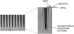
- a second embodimentuses a through hole via that may have the ceramic phase etched with a dilute HF solution to create a textured high surface area on one side or both sides to partially or fully remove the glass-ceramic as the base substrate for the capacitive structure.
- a third embodimentuse a posts on one or both sides of the APEX® Glass substrate that may have the ceramic phase etched with a dilute HF to create to a high surface area capacitive structure.
Landscapes
- Engineering & Computer Science (AREA)
- Power Engineering (AREA)
- Microelectronics & Electronic Packaging (AREA)
- Manufacturing & Machinery (AREA)
- Chemical & Material Sciences (AREA)
- Inorganic Chemistry (AREA)
- Ceramic Engineering (AREA)
- Materials Engineering (AREA)
- Glass Compositions (AREA)
- Ceramic Capacitors (AREA)
- Fixed Capacitors And Capacitor Manufacturing Machines (AREA)
- Internal Circuitry In Semiconductor Integrated Circuit Devices (AREA)
- Micromachines (AREA)
- Semiconductor Integrated Circuits (AREA)
Abstract
Description
Ce3++Ag+=□Ce4++Ag0
Claims (13)
Priority Applications (1)
| Application Number | Priority Date | Filing Date | Title |
|---|---|---|---|
| US16/079,033US11264167B2 (en) | 2016-02-25 | 2017-02-24 | 3D capacitor and capacitor array fabricating photoactive substrates |
Applications Claiming Priority (3)
| Application Number | Priority Date | Filing Date | Title |
|---|---|---|---|
| US201662299641P | 2016-02-25 | 2016-02-25 | |
| US16/079,033US11264167B2 (en) | 2016-02-25 | 2017-02-24 | 3D capacitor and capacitor array fabricating photoactive substrates |
| PCT/US2017/019483WO2017147511A1 (en) | 2016-02-25 | 2017-02-24 | 3d capacitor and capacitor array fabricating photoactive substrates |
Related Parent Applications (1)
| Application Number | Title | Priority Date | Filing Date |
|---|---|---|---|
| PCT/US2017/019483A-371-Of-InternationalWO2017147511A1 (en) | 2016-02-25 | 2017-02-24 | 3d capacitor and capacitor array fabricating photoactive substrates |
Related Child Applications (1)
| Application Number | Title | Priority Date | Filing Date |
|---|---|---|---|
| US17/584,543Continuation-In-PartUS12165809B2 (en) | 2016-02-25 | 2022-01-26 | 3D capacitor and capacitor array fabricating photoactive substrates |
Publications (2)
| Publication Number | Publication Date |
|---|---|
| US20190074136A1 US20190074136A1 (en) | 2019-03-07 |
| US11264167B2true US11264167B2 (en) | 2022-03-01 |
Family
ID=59686662
Family Applications (1)
| Application Number | Title | Priority Date | Filing Date |
|---|---|---|---|
| US16/079,033ActiveUS11264167B2 (en) | 2016-02-25 | 2017-02-24 | 3D capacitor and capacitor array fabricating photoactive substrates |
Country Status (7)
| Country | Link |
|---|---|
| US (1) | US11264167B2 (en) |
| EP (1) | EP3420571A4 (en) |
| JP (3) | JP7071609B2 (en) |
| KR (3) | KR20180134868A (en) |
| AU (1) | AU2017223993B2 (en) |
| CA (1) | CA3015525C (en) |
| WO (1) | WO2017147511A1 (en) |
Cited By (2)
| Publication number | Priority date | Publication date | Assignee | Title |
|---|---|---|---|---|
| US11908617B2 (en) | 2020-04-17 | 2024-02-20 | 3D Glass Solutions, Inc. | Broadband induction |
| US12431627B2 (en) | 2018-07-13 | 2025-09-30 | Knowles Cazenovia, Inc. | Millimeter wave filter array |
Families Citing this family (24)
| Publication number | Priority date | Publication date | Assignee | Title |
|---|---|---|---|---|
| EP3140838B1 (en) | 2014-05-05 | 2021-08-25 | 3D Glass Solutions, Inc. | Inductive device in a photo-definable glass structure |
| US10070533B2 (en) | 2015-09-30 | 2018-09-04 | 3D Glass Solutions, Inc. | Photo-definable glass with integrated electronics and ground plane |
| KR20180134868A (en) | 2016-02-25 | 2018-12-19 | 3디 글래스 솔루션즈 인코포레이티드 | A photoactive substrate for fabricating 3D capacitors and capacitor arrays |
| US11161773B2 (en) | 2016-04-08 | 2021-11-02 | 3D Glass Solutions, Inc. | Methods of fabricating photosensitive substrates suitable for optical coupler |
| KR102273624B1 (en) | 2017-04-28 | 2021-07-07 | 3디 글래스 솔루션즈 인코포레이티드 | Rf Circulator |
| KR102418671B1 (en) | 2017-07-07 | 2022-07-12 | 3디 글래스 솔루션즈 인코포레이티드 | 2d and 3d rf lumped element devices for rf system in a package photoactive glass substrates |
| JP7008824B2 (en) | 2017-12-15 | 2022-01-25 | スリーディー グラス ソリューションズ,インク | Connection transmission line resonant RF filter |
| EP3735743A4 (en)* | 2018-01-04 | 2021-03-03 | 3D Glass Solutions, Inc. | Impedance matching conductive structure for high efficiency rf circuits |
| CN108390065A (en)* | 2018-01-25 | 2018-08-10 | 湖北师范大学 | A method of in li-ion electrode materials surface coating cerium oxide |
| EP3643148A4 (en)* | 2018-04-10 | 2021-03-31 | 3D Glass Solutions, Inc. | INTEGRATED RF POWER CONDITIONING CAPACITOR |
| US10903545B2 (en) | 2018-05-29 | 2021-01-26 | 3D Glass Solutions, Inc. | Method of making a mechanically stabilized radio frequency transmission line device |
| EP3637448A4 (en)* | 2018-08-21 | 2020-10-07 | Shenzhen Weitongbo Technology Co., Ltd. | CAPACITOR AND MANUFACTURING METHOD FOR IT |
| US11139582B2 (en) | 2018-09-17 | 2021-10-05 | 3D Glass Solutions, Inc. | High efficiency compact slotted antenna with a ground plane |
| AU2019416325A1 (en) | 2018-12-28 | 2021-02-04 | 3D Glass Solutions, Inc. | Heterogenous integration for RF, microwave and mm wave systems in photoactive glass substrates |
| AU2019416327B2 (en) | 2018-12-28 | 2021-12-09 | 3D Glass Solutions, Inc. | Annular capacitor RF, microwave and MM wave systems |
| EP3723148A1 (en)* | 2019-04-08 | 2020-10-14 | Murata Manufacturing Co., Ltd. | Three-dimensional capacitive structures and their manufacturing methods |
| KR102601781B1 (en)* | 2019-04-18 | 2023-11-14 | 3디 글래스 솔루션즈 인코포레이티드 | High efficiency die dicing and release |
| CA3156811A1 (en)* | 2019-10-14 | 2021-04-22 | 3D Glass Solutions, Inc. | High temperature printed circuit board substrate |
| WO2021183440A1 (en)* | 2020-03-11 | 2021-09-16 | 3D Glass Solutions, Inc. | Ultra high surface area integrated capacitor |
| KR20240019226A (en)* | 2021-06-04 | 2024-02-14 | 3디 글래스 솔루션즈 인코포레이티드 | Ceramic capacitors devices for RF systems on photoactive glass substrates |
| WO2022265783A1 (en)* | 2021-06-15 | 2022-12-22 | 3D Glass Solutions, Inc. | Radio frequency (rf) integrated power-conditioning capacitor |
| KR20240095180A (en)* | 2021-09-03 | 2024-06-25 | 3디 글래스 솔루션즈 인코포레이티드 | Power amplifier system-in-package |
| WO2023146729A1 (en)* | 2022-01-26 | 2023-08-03 | 3D Glass Solutions, Inc. | 3d capacitor and capacitor array fabricating photoactive substrates |
| US12424518B2 (en)* | 2022-02-28 | 2025-09-23 | Qualcomm Incorporated | Capacitor embedded 3D resonator for broadband filter |
Citations (227)
| Publication number | Priority date | Publication date | Assignee | Title |
|---|---|---|---|---|
| US2515940A (en) | 1946-09-09 | 1950-07-18 | Corning Glass Works | Photosensitive opal glass |
| US2515941A (en) | 1946-09-09 | 1950-07-18 | Corning Glass Works | Photosensitive opal glass |
| US2628160A (en) | 1951-08-30 | 1953-02-10 | Corning Glass Works | Sculpturing glass |
| US2684911A (en) | 1951-08-30 | 1954-07-27 | Corning Glass Works | Photosensitively opacifiable glass |
| US2971853A (en) | 1953-03-05 | 1961-02-14 | Corning Glass Works | Ceramic body and method of making it |
| US3904991A (en) | 1973-02-12 | 1975-09-09 | Tokyo Shibaura Electric Co | Stripline directional coupler having bent coupling arms |
| US3985531A (en) | 1975-03-19 | 1976-10-12 | Corning Glass Works | Spontaneously-formed fluormica glass-ceramics |
| US3993401A (en) | 1975-02-10 | 1976-11-23 | Minnesota Mining And Manufacturing Company | Retroreflective material including geometric fresnel zone plates |
| US4029605A (en) | 1975-12-08 | 1977-06-14 | Hercules Incorporated | Metallizing compositions |
| US4131516A (en) | 1977-07-21 | 1978-12-26 | International Business Machines Corporation | Method of making metal filled via holes in ceramic circuit boards |
| JPS56155587A (en) | 1980-05-02 | 1981-12-01 | Fujitsu Ltd | Printed circuit board |
| US4413061A (en) | 1978-02-06 | 1983-11-01 | International Business Machines Corporation | Glass-ceramic structures and sintered multilayer substrates thereof with circuit patterns of gold, silver or copper |
| US4444616A (en) | 1981-06-02 | 1984-04-24 | Hoya Corporation | Method for exposure of chemically machinable light-sensitive glass |
| US4514053A (en) | 1983-08-04 | 1985-04-30 | Corning Glass Works | Integral photosensitive optical device and method |
| US4537612A (en) | 1982-04-01 | 1985-08-27 | Corning Glass Works | Colored photochromic glasses and method |
| JPS61149905A (en) | 1984-12-25 | 1986-07-08 | Fujitsu Ltd | Optical multiplexer and demultiplexer |
| JPS61231529A (en) | 1985-04-08 | 1986-10-15 | Agency Of Ind Science & Technol | Optical control type optical switch device |
| US4647940A (en) | 1982-09-27 | 1987-03-03 | Rogers Corporation | Parallel plate waveguide antenna |
| JPS62202840A (en) | 1986-03-03 | 1987-09-07 | Toshiba Corp | Working of photosensitive glass |
| US4692015A (en) | 1986-03-14 | 1987-09-08 | Xerox Corporation | Short focal lens array with multi-magnification properties |
| JPS63128699A (en) | 1986-11-19 | 1988-06-01 | 株式会社日立製作所 | Light-sensitive glass-ceramic multilayer interconnection board |
| US4788165A (en) | 1987-10-07 | 1988-11-29 | Corning Glass Works | Copper-exuding, boroaluminosilicate glasses |
| EP0311274A2 (en) | 1987-10-07 | 1989-04-12 | Corning Glass Works | Thermal writing on glass or glass-ceramic substrates and copper-exuding glasses |
| US4942076A (en) | 1988-11-03 | 1990-07-17 | Micro Substrates, Inc. | Ceramic substrate with metal filled via holes for hybrid microcircuits and method of making the same |
| JPH0393683A (en) | 1989-09-01 | 1991-04-18 | Fujitsu Ltd | Copper paste and metallization method using the same |
| US5078771A (en) | 1989-02-07 | 1992-01-07 | Canyon Materials, Inc. | Method of making high energy beam sensitive glasses |
| US5147740A (en) | 1990-08-09 | 1992-09-15 | Rockwell International Corporation | Structure and process for fabricating conductive patterns having sub-half micron dimensions |
| EP0507719A1 (en) | 1991-04-04 | 1992-10-07 | International Business Machines Corporation | Improved glass-ceramic to copper adhesion |
| US5212120A (en) | 1991-06-10 | 1993-05-18 | Corning Incorporated | Photosensitive glass |
| JPH05139787A (en) | 1991-11-19 | 1993-06-08 | Seikosha Co Ltd | Working method for photosensitive glass |
| US5371466A (en) | 1992-07-29 | 1994-12-06 | The Regents Of The University Of California | MRI RF ground breaker assembly |
| US5374291A (en) | 1991-12-10 | 1994-12-20 | Director-General Of Agency Of Industrial Science And Technology | Method of processing photosensitive glass |
| US5395498A (en) | 1991-11-06 | 1995-03-07 | Gombinsky; Moshe | Method for separating biological macromolecules and means therfor |
| US5409741A (en) | 1991-04-12 | 1995-04-25 | Laude; Lucien D. | Method for metallizing surfaces by means of metal powders |
| JPH0826767A (en) | 1994-07-13 | 1996-01-30 | Nippon Glass Kk | Soda lime-silica photosensitive glass and its production |
| JPH08179155A (en) | 1994-12-26 | 1996-07-12 | Ricoh Co Ltd | Method for coupling lens and optical fiber and method for producing lens substrate |
| JPH107435A (en) | 1996-06-26 | 1998-01-13 | Ngk Spark Plug Co Ltd | Glass ceramic wiring substrate and its production |
| US5733370A (en) | 1996-01-16 | 1998-03-31 | Seagate Technology, Inc. | Method of manufacturing a bicrystal cluster magnetic recording medium |
| US5779521A (en) | 1995-03-03 | 1998-07-14 | Sony Corporation | Method and apparatus for chemical/mechanical polishing |
| JPH10199728A (en) | 1997-01-07 | 1998-07-31 | Murata Mfg Co Ltd | Thin-film coil component and method of manufacturing the same |
| US5850623A (en) | 1997-03-14 | 1998-12-15 | Eastman Chemical Company | Method for standardizing raman spectrometers to obtain stable and transferable calibrations |
| US5902715A (en) | 1992-11-09 | 1999-05-11 | Fujitsu Limited | Method of forming a mirror in a waveguide |
| US5919607A (en) | 1995-10-26 | 1999-07-06 | Brown University Research Foundation | Photo-encoded selective etching for glass based microtechnology applications |
| EP0685857B1 (en) | 1994-06-03 | 1999-09-08 | Mitel Semiconductor Limited | Inductor chip device |
| EP0949648A1 (en) | 1996-09-26 | 1999-10-13 | Asahi Glass Company Ltd. | Plasma display protective plate and its manufacturing method |
| US5998224A (en) | 1997-05-16 | 1999-12-07 | Abbott Laboratories | Magnetically assisted binding assays utilizing a magnetically responsive reagent |
| JPH11344648A (en) | 1998-05-07 | 1999-12-14 | Trw Inc | Fiber/waveguide-mirror-lens alignment device |
| US6066448A (en) | 1995-03-10 | 2000-05-23 | Meso Sclae Technologies, Llc. | Multi-array, multi-specific electrochemiluminescence testing |
| US6094336A (en) | 1997-04-25 | 2000-07-25 | U.S. Philips Corporation | Enveloped multilayer capacitor |
| JP2000228615A (en) | 1999-02-05 | 2000-08-15 | Tokin Corp | Lc bandpass filter |
| US6136210A (en) | 1998-11-02 | 2000-10-24 | Xerox Corporation | Photoetching of acoustic lenses for acoustic ink printing |
| US6171886B1 (en) | 1998-06-30 | 2001-01-09 | Eastman Kodak Company | Method of making integrated hybrid silicon-based micro-actuator devices |
| JP2001033664A (en) | 1999-07-21 | 2001-02-09 | Hitachi Cable Ltd | Optical fiber block |
| US6258497B1 (en) | 1992-07-29 | 2001-07-10 | International Business Machines Corporation | Precise endpoint detection for etching processes |
| JP2001206735A (en) | 2000-01-25 | 2001-07-31 | Central Glass Co Ltd | Plating method |
| US6287965B1 (en) | 1997-07-28 | 2001-09-11 | Samsung Electronics Co, Ltd. | Method of forming metal layer using atomic layer deposition and semiconductor device having the metal layer as barrier metal layer or upper or lower electrode of capacitor |
| US6329702B1 (en) | 2000-07-06 | 2001-12-11 | Tyco Electronics Corporation | High frequency carrier |
| US20010051584A1 (en) | 2000-04-26 | 2001-12-13 | Matsushita Electric Industrial Co., Ltd. | Dielectric ceramic composition and method for producing the same, and device for communication apparatus using the same |
| US20020015546A1 (en) | 2000-07-31 | 2002-02-07 | Bhagavatula Venkata A. | Bulk internal bragg gratings and optical devices |
| US6373369B2 (en) | 1999-07-26 | 2002-04-16 | Taiwan Semiconductor Manufacturing Company | High efficiency thin film inductor |
| US6383566B1 (en) | 1999-06-30 | 2002-05-07 | Saint-Gobain Vitrage | Process for depositing a tungsten-based and/or molybdenum-based layer on a rigid substrate, and substrate thus coated |
| US20020086246A1 (en) | 2000-12-30 | 2002-07-04 | Lg Electronics Inc. | Method of fabricating barrier ribs in plasma display panel |
| US20020100608A1 (en) | 1999-05-27 | 2002-08-01 | Hoya Corporation | Multilayer printed wiring board and a process of producing same |
| US6485690B1 (en) | 1999-05-27 | 2002-11-26 | Orchid Biosciences, Inc. | Multiple fluid sample processor and system |
| US6511793B1 (en) | 1999-03-24 | 2003-01-28 | Lg Electronics Inc. | Method of manufacturing microstructure using photosensitive glass substrate |
| US6514375B2 (en) | 1997-12-15 | 2003-02-04 | Ricoh Company, Ltd. | Dry etching endpoint detection system |
| US20030025227A1 (en) | 2001-08-02 | 2003-02-06 | Zograph, Llc | Reproduction of relief patterns |
| US6562523B1 (en) | 1996-10-31 | 2003-05-13 | Canyon Materials, Inc. | Direct write all-glass photomask blanks |
| US20030124716A1 (en) | 2000-10-10 | 2003-07-03 | Biotrove, Inc., A Delaware Corporation | Apparatus for assay, synthesis and storage, and methods of manufacture, use, and manipulation thereof |
| US20030135201A1 (en) | 2001-09-28 | 2003-07-17 | Gonnelli Robert R. | Microneedle with membrane |
| US20030156819A1 (en) | 2002-02-15 | 2003-08-21 | Mark Pruss | Optical waveguide |
| US20030174944A1 (en) | 2002-03-14 | 2003-09-18 | Corning Incorporated | Fiber array and methods for fabricating the fiber array |
| US20030228682A1 (en) | 2002-04-30 | 2003-12-11 | University Of Maryland, Baltimore | Fluorescence sensing |
| US20030231830A1 (en) | 2002-05-14 | 2003-12-18 | Naoko Hikichi | Optical module |
| US6678453B2 (en) | 1999-11-04 | 2004-01-13 | Corning Incorporated | High aspect ratio patterning of glass film |
| US20040008391A1 (en) | 1999-09-16 | 2004-01-15 | Bowley Christopher C. | Holographically-formed polymer dispersed liquid crystals with multiple gratings |
| US6686824B1 (en) | 1998-05-29 | 2004-02-03 | Nissha Printing Co., Ltd. | Toroidal printed coil |
| US20040020690A1 (en) | 1998-03-20 | 2004-02-05 | Parker John Leroy | Via connector and method of making same |
| US20040155748A1 (en) | 2003-02-02 | 2004-08-12 | Dietrich Steingroever | Transformer for producing high electrical currents |
| US6783920B2 (en) | 2003-01-15 | 2004-08-31 | The Aerospace Corporation | Photosensitive glass variable laser exposure patterning method |
| US20040171076A1 (en) | 2001-12-20 | 2004-09-02 | Dejneka Matthew J. | Detectable micro to nano sized structures, methods of manufacture and use |
| US20040184705A1 (en) | 2003-01-08 | 2004-09-23 | Mikihiro Shimada | Optical waveguide component and method of manufacturing the same |
| US20040198582A1 (en) | 2003-04-01 | 2004-10-07 | Borrelli Nicholas F. | Optical elements and methods of making optical elements |
| US20040227596A1 (en) | 2003-02-11 | 2004-11-18 | Nguyen John A. | Ultra broadband inductor assembly |
| US6824974B2 (en) | 2001-06-11 | 2004-11-30 | Genorx, Inc. | Electronic detection of biological molecules using thin layers |
| CN1562831A (en) | 2004-04-16 | 2005-01-12 | 武汉理工大学 | Method for preparing microcrystalline glass/glass carrier material having nano holes in high density |
| US6843902B1 (en) | 2001-07-20 | 2005-01-18 | The Regents Of The University Of California | Methods for fabricating metal nanowires |
| US6875544B1 (en) | 2002-10-03 | 2005-04-05 | Sandia Corporation | Method for the fabrication of three-dimensional microstructures by deep X-ray lithography |
| US20050089901A1 (en) | 2000-09-22 | 2005-04-28 | Porter Marc D. | Raman-active reagents and the use thereof |
| US20050105860A1 (en) | 2003-02-24 | 2005-05-19 | Ngk Spark Plug Co., Ltd. | Optical device mounted substrate assembly |
| US20050150683A1 (en) | 2004-01-12 | 2005-07-14 | Farnworth Warren M. | Methods of fabricating substrates and substrate precursor structures resulting therefrom |
| US20050170670A1 (en) | 2003-11-17 | 2005-08-04 | King William P. | Patterning of sacrificial materials |
| JP2005215644A (en) | 2004-02-02 | 2005-08-11 | Sharp Corp | Optical module and manufacturing method thereof |
| US6932933B2 (en) | 2001-03-30 | 2005-08-23 | The Aerospace Corporation | Ultraviolet method of embedding structures in photocerams |
| JP2005302987A (en) | 2004-04-12 | 2005-10-27 | Dainippon Printing Co Ltd | Passive element built-in wiring board and manufacturing method thereof |
| US20050277550A1 (en) | 2004-06-09 | 2005-12-15 | Ferro Corporation | Lead-free and cadmium-free conductive copper thick film pastes |
| US6977722B2 (en) | 2001-06-29 | 2005-12-20 | Meso Scale Technologies, Llc. | Assay plates, reader systems and methods for luminescence test measurements |
| DE102004059252A1 (en) | 2004-06-09 | 2006-01-19 | Schott Ag | Optically active structure application method for Fresnel lens manufacture, involves photographic structuring photosensitive resist layer, coating substrate with optically active layer and lifting-off resist layer |
| US7033821B2 (en) | 2000-11-08 | 2006-04-25 | Surface Logix, Inc. | Device for monitoring cell motility in real-time |
| US20060092079A1 (en) | 2004-10-01 | 2006-05-04 | De Rochemont L P | Ceramic antenna module and methods of manufacture thereof |
| US20060118965A1 (en) | 2004-12-02 | 2006-06-08 | Nec Electronics Corporation | Semiconductor device, semiconductor module employing thereof and method for manufacturing semiconductor device |
| JP2006179564A (en) | 2004-12-21 | 2006-07-06 | Nec Corp | Semiconductor connection substrate, method of manufacturing the same semiconductor apparatus, semiconductor device, and semiconductor substrate |
| US20060147344A1 (en) | 2004-09-30 | 2006-07-06 | The University Of Cincinnati | Fully packed capillary electrophoretic separation microchips with self-assembled silica colloidal particles in microchannels and their preparation methods |
| US20060158300A1 (en) | 2005-01-20 | 2006-07-20 | Avx Corporation | High Q planar inductors and IPD applications |
| US20060159916A1 (en) | 2003-05-05 | 2006-07-20 | Nanosys, Inc. | Nanofiber surfaces for use in enhanced surface area applications |
| EP1683571A1 (en) | 2005-01-20 | 2006-07-26 | Samsung Electronics Co., Ltd. | Patterning method, substrate for biomolecule immobilization using the patterning method, and biochip employing the substrate |
| US20060177866A1 (en) | 1999-03-03 | 2006-08-10 | O'brien Timothy J | Transmembrane serine protease overexpressed in ovarian carcinoma and uses thereof |
| US20060193214A1 (en) | 2005-02-28 | 2006-08-31 | Takeshi Shimano | Optical head, optical information storage apparatus, and their fabrication method |
| US7132054B1 (en) | 2004-09-08 | 2006-11-07 | Sandia Corporation | Method to fabricate hollow microneedle arrays |
| US20060283948A1 (en) | 2005-06-20 | 2006-12-21 | Denso Corporation | Antenna coil, resonant antenna having antenna coil, and card type wireless device having resonant antenna |
| US7179638B2 (en) | 1999-07-30 | 2007-02-20 | Large Scale Biology Corporation | Microarrays and their manufacture by slicing |
| US20070120263A1 (en) | 2005-08-19 | 2007-05-31 | Zvonimir Gabric | Conductor track arrangement and associated production method |
| US20070121263A1 (en) | 2005-11-29 | 2007-05-31 | Jeng-Shu Liu | Timing controller chip |
| US20070155021A1 (en) | 2005-12-29 | 2007-07-05 | Intel Corporation | Modification of metal nanoparticles for improved analyte detection by surface enhanced Raman spectroscopy (SERS) |
| US20070158787A1 (en) | 2003-11-13 | 2007-07-12 | Rajen Chanchani | Heterogeneously integrated microsystem-on-a-chip |
| WO2007088058A2 (en) | 2006-02-02 | 2007-08-09 | Xsil Technology Limited | Support for wafer singulation |
| US7277151B2 (en) | 2001-10-15 | 2007-10-02 | Samsung Sdi Co., Ltd. | Flat panel display with photosensitive glass spacer |
| US20070248126A1 (en) | 2002-06-10 | 2007-10-25 | New Wave Research | Scribing sapphire substrates with a solid state uv laser |
| US20070267708A1 (en) | 2006-05-22 | 2007-11-22 | Cardiomems, Inc. | Methods and apparatus having an integrated circuit attached to fused silica |
| US20070272829A1 (en) | 2006-05-29 | 2007-11-29 | Atsuo Nakagawa | Solid-state imaging device and method for fabricating the same |
| US20070279837A1 (en) | 2004-03-18 | 2007-12-06 | Nanosys, Inc. | Nanofiber Surface Based Capacitors |
| US7306689B2 (en) | 1998-10-27 | 2007-12-11 | Sony Corporation | Optical waveguide and method for producing same |
| US20070296520A1 (en) | 2005-04-18 | 2007-12-27 | Murata Manufacturing Co., Ltd. | High-frequency module |
| US7326538B2 (en) | 2002-01-04 | 2008-02-05 | Becton Dickinson And Company | Binding proteins as biosensors |
| US20080136572A1 (en) | 2006-12-06 | 2008-06-12 | Farrokh Ayazi | Micro-electromechanical switched tunable inductor |
| US20080174976A1 (en) | 2001-07-12 | 2008-07-24 | Hitachi, Ltd. | Electronic Circuit Component |
| US20080182079A1 (en) | 2006-06-28 | 2008-07-31 | Northwestern University | Etching and hole arrays |
| US7407768B2 (en) | 2002-09-11 | 2008-08-05 | Synamem Corporation | Membrane-based assays |
| US7410763B2 (en) | 2005-09-01 | 2008-08-12 | Intel Corporation | Multiplex data collection and analysis in bioanalyte detection |
| US20080223603A1 (en) | 2007-03-12 | 2008-09-18 | Samsung Electro-Mechanics Co., Ltd. | Capacitor embedded printed circuit board |
| US20080226228A1 (en) | 2007-03-15 | 2008-09-18 | Hitachi Cable, Ltd. | Optical system connection structure, optical component, and optical communication module |
| WO2008119080A1 (en) | 2007-03-28 | 2008-10-02 | Life Bioscience Inc. | Compositions and methods to fabricate a photoactive substrate suitable for shaped glass structures |
| JP2008252797A (en) | 2007-03-30 | 2008-10-16 | Tdk Corp | Dielectric resonator, dielectric filter, and characteristic adjustment method thereof |
| US7439128B2 (en) | 2003-04-07 | 2008-10-21 | International Business Machines Corporation | Method of creating deep trench capacitor using a P+ metal electrode |
| US20080291442A1 (en) | 2005-06-13 | 2008-11-27 | Solaris Nanosciences, Inc. | Chemical and biological sensing using metallic particles in amplifying and absorbing media |
| US20080305268A1 (en) | 2007-06-05 | 2008-12-11 | Air Products And Chemicals, Inc. | Low Temperature Thermal Conductive Inks |
| WO2008154931A1 (en) | 2007-06-18 | 2008-12-24 | Danmarks Tekniske Universitet (Technical University Of Denmark) | Adsorbent beads suitable for use in separation of biological molecules |
| US20080316678A1 (en) | 2006-07-14 | 2008-12-25 | Ehrenberg Scott G | Nanoparticle ultracapacitor |
| US7470518B2 (en) | 2002-02-12 | 2008-12-30 | Cellectricon Ab | Systems and method for rapidly changing the solution environment around sensors |
| US20090029185A1 (en) | 2007-07-27 | 2009-01-29 | Cheng-Chang Lee | Magnetic device and manufacturing method thereof |
| US7497554B2 (en) | 2004-07-22 | 2009-03-03 | Konica Minolta Holdings, Inc. | Ink jet print head |
| WO2009029733A2 (en) | 2007-08-28 | 2009-03-05 | Life Biosciences, Inc. | Method of providing a pattern of biological-binding areas for biological testing |
| WO2009062011A1 (en) | 2007-11-07 | 2009-05-14 | Masachusetts Institute Of Technology | Method of forming a locally periodic 3d structure with larger-scale variation in periodic properties and applications thereof |
| US20090130736A1 (en) | 2003-02-06 | 2009-05-21 | Becton, Dickinson And Company | Pretreatment method for extraction of nucleic acid from biological samples and kits therefor |
| US20090170032A1 (en) | 2007-12-28 | 2009-07-02 | Fujitsu Media Devices Limited | Method of manufacturing electronic device |
| US20090182720A1 (en) | 2008-01-15 | 2009-07-16 | Cain Michael W | Maintained Symbol Table Only Index |
| US20090243783A1 (en) | 2006-08-28 | 2009-10-01 | Avago Technologies Ecbu (Singapore) Pte. Ltd. | Minimizing Electromagnetic Interference in Coil Transducers |
| WO2009126649A2 (en) | 2008-04-07 | 2009-10-15 | Life Bioscience, Inc. | Method of providing particles having biological-binding areas for biological applications |
| WO2010011939A2 (en) | 2008-07-25 | 2010-01-28 | Life Bioscience, Inc. | Assay plates, methods and systems having one or more etched features |
| KR100941691B1 (en) | 2009-04-10 | 2010-02-12 | (주)제이스 | Photosensitve glass wafer and method for manufacturing potosensitve glass wafer and semiconductor probe chip |
| US20100059265A1 (en) | 2008-09-11 | 2010-03-11 | Myung-Soo Kim | Contact of semiconductor device and manufacturing method thereof |
| US20100237462A1 (en) | 2009-03-18 | 2010-09-23 | Benjamin Beker | Package Level Tuning Techniques for Propagation Channels of High-Speed Signals |
| US20110003422A1 (en) | 2009-07-02 | 2011-01-06 | Advanced Microfab, LLC | Method of forming monolithic cmos-mems hybrid integrated, packaged structures |
| US20110045284A1 (en) | 2008-03-12 | 2011-02-24 | Dai Nippon Printing Co., Ltd. | Decorative sheet for three-dimensional work |
| US20110065662A1 (en) | 2009-07-24 | 2011-03-17 | Amazentis Sa | Compounds, Compositions, and Methods for Protecting Brain Health in Neurodegenerative Disorders |
| US20110108525A1 (en) | 2009-11-11 | 2011-05-12 | Industrial Technology Research Institute | Method and system for manufacturing microstructure in photosensitive glass substrate |
| US7948342B2 (en) | 2008-07-24 | 2011-05-24 | Cutt-A-Watt Enterprises, Llc | Electromotive rectification system |
| US20110170273A1 (en) | 2010-01-13 | 2011-07-14 | The Aerospace Corporation | Photostructured Magnetic Devices and Methods for Making Same |
| US20110195360A1 (en) | 2010-02-10 | 2011-08-11 | Life Bioscience, Inc. | Methods to fabricate a photoactive substrate suitable for microfabrication |
| US20110217657A1 (en) | 2010-02-10 | 2011-09-08 | Life Bioscience, Inc. | Methods to fabricate a photoactive substrate suitable for microfabrication |
| WO2011109648A1 (en) | 2010-03-03 | 2011-09-09 | Georgia Tech Research Corporation | Through-package-via (tpv) structures on inorganic interposer and methods for fabricating same |
| US8062753B2 (en) | 2004-12-31 | 2011-11-22 | Schott Ag | Method for producing an optical component, optical component produced according to the method and devices comprising such components |
| US20110284725A1 (en) | 2008-03-04 | 2011-11-24 | The Regents Of The Univeristy Of California | Microlens arrays for enhanced light concentration |
| US20110304999A1 (en) | 2010-06-10 | 2011-12-15 | Taiwan Semiconductor Manufacturing Company, Ltd. | Interposer-on-Glass Package Structures |
| US20120080612A1 (en) | 2009-04-03 | 2012-04-05 | Research Triangle Institute | Cantilever-based mems optical scanning apparatus, system and method |
| JP2012079960A (en) | 2010-10-04 | 2012-04-19 | Denso Corp | Capacitor structure and method for manufacturing the same |
| WO2012078213A1 (en) | 2010-12-09 | 2012-06-14 | Tessera Inc | High density three-dimensional integrated capacitors |
| US20120161330A1 (en) | 2010-12-22 | 2012-06-28 | Intel Corporation | Device packaging with substrates having embedded lines and metal defined pads |
| KR101167691B1 (en) | 2011-08-09 | 2012-07-20 | 주식회사 비티엔아이티솔루션스 | Multilayer capacitor having photosensitive glass, fabrication method thereof, and the use the same |
| JP2013062473A (en) | 2011-09-15 | 2013-04-04 | Toppan Printing Co Ltd | Wiring board and manufacturing method therefor |
| US20130119401A1 (en) | 2010-06-18 | 2013-05-16 | Soraa, Inc. | Large area nitride crystal and method for making it |
| US20130183805A1 (en) | 2010-09-14 | 2013-07-18 | International Business Machines Corporation | High capacitance trench capacitor |
| US20130233202A1 (en) | 2010-12-03 | 2013-09-12 | Ei Du Pont De Nemours And Company | Inks and processes for preparing copper indium gallium sulfide/selenide coatings and films |
| JP2013217989A (en) | 2012-04-04 | 2013-10-24 | Hitachi Chemical Co Ltd | Optical fiber connector |
| US20130278568A1 (en) | 2012-04-24 | 2013-10-24 | Qualcomm Mems Technologies, Inc. | Metal-insulator-metal capacitors on glass substrates |
| US20130308906A1 (en) | 2012-05-21 | 2013-11-21 | LaXense, Inc. | System and method for dense coupling between optical devices and an optical fiber array |
| US20130337604A1 (en) | 2012-06-19 | 2013-12-19 | E I Du Pont De Nemours And Company | Method of manufacturing thick-film electrode |
| US20140002906A1 (en) | 2011-03-17 | 2014-01-02 | Enplas Corporation | Lens array |
| US20140035892A1 (en) | 2012-08-03 | 2014-02-06 | Qualcomm Mems Technologies, Inc. | Incorporation of passives and fine pitch through via for package on package |
| US20140035540A1 (en) | 2012-02-08 | 2014-02-06 | Dais Analytic Corporation | Energy storage device and methods |
| US20140035935A1 (en) | 2012-08-03 | 2014-02-06 | Qualcomm Mems Technologies, Inc. | Passives via bar |
| US20140070380A1 (en) | 2012-09-11 | 2014-03-13 | Chia-Pin Chiu | Bridge interconnect with air gap in package assembly |
| WO2014043267A1 (en) | 2012-09-12 | 2014-03-20 | Life Bioscience, Inc. | Methods of fabricating photoactive substrates suitable for electromagnetic transmission and filtering applications |
| US20140104284A1 (en) | 2012-10-16 | 2014-04-17 | Qualcomm Mems Technologies, Inc. | Through substrate via inductors |
| WO2014062226A1 (en) | 2012-10-19 | 2014-04-24 | Rutgers, The State University Of New Jersey | In situ exfoliation method to fabricate a graphene-reinforced polymer matrix composite |
| US20140145326A1 (en) | 2012-11-29 | 2014-05-29 | United Microelectronics Corp. | Substrate with integrated passive devices and method of manufacturing the same |
| US20140144681A1 (en) | 2012-11-27 | 2014-05-29 | Qualcomm Mems Technologies, Inc. | Adhesive metal nitride on glass and related methods |
| US20140169746A1 (en) | 2012-12-14 | 2014-06-19 | Hon Hai Precision Industry Co., Ltd. | Optical connector with sloped surface |
| US20140203891A1 (en) | 2012-01-16 | 2014-07-24 | Murata Manufacturing Co., Ltd. | Rf signal blocking device |
| US20140247269A1 (en) | 2013-03-04 | 2014-09-04 | Qualcomm Mems Technologies, Inc. | High density, low loss 3-d through-glass inductor with magnetic core |
| US20140272688A1 (en) | 2013-03-15 | 2014-09-18 | Photronics, Inc. | Grayscale lithography of photo definable glass |
| US20140367695A1 (en) | 2013-06-18 | 2014-12-18 | Stephen P. Barlow | Trench high electron mobility transistor device |
| JP2014241365A (en) | 2013-06-12 | 2014-12-25 | 株式会社デンソー | Penetration type capacitor |
| JP2015028651A (en) | 2006-12-22 | 2015-02-12 | シスコ テクノロジー,インコーポレイテッド | Dual-lensed unitary optical receiver assembly |
| US20150048901A1 (en) | 2013-08-19 | 2015-02-19 | Harris Corporation | Microelectromechanical systems comprising differential inductors and methods for making the same |
| US20150071593A1 (en) | 2012-03-28 | 2015-03-12 | Enplas Corporation | Optical receptacle and optical module comprising same |
| WO2015108648A1 (en) | 2014-01-14 | 2015-07-23 | Qualcomm Incorporated | A stacked conductive interconnect inductor |
| US20150210074A1 (en) | 2012-08-16 | 2015-07-30 | Chien-Hua Chen | Diagonal openings in photodefinable glass |
| WO2015112903A1 (en) | 2014-01-24 | 2015-07-30 | 3D Glass Solutions, Inc | Methods of fabricating photoactive substrates for micro-lenses and arrays |
| US20150263429A1 (en) | 2011-08-31 | 2015-09-17 | Mehrnoosh Vahidpour | Micromachined millimeter-wave frequency scanning array |
| WO2015171597A1 (en) | 2014-05-05 | 2015-11-12 | 3D Glass Solutions, Inc. | 2d and 3d inductors antenna and transformers fabricating photoactive substrates |
| US20160048079A1 (en) | 2014-08-12 | 2016-02-18 | Su-Young Lee | Method, photolithography method, and method of manufacturing a semiconductor device using a pellicle film |
| US20160181211A1 (en) | 2013-09-27 | 2016-06-23 | Intel Corporation | Die package with superposer substrate for passive components |
| US20160185653A1 (en) | 2013-09-04 | 2016-06-30 | Hoya Corporation | Silicate ceramics, plate-like substrate, and method of producing plate-like substrate |
| US9385083B1 (en) | 2015-05-22 | 2016-07-05 | Hrl Laboratories, Llc | Wafer-level die to package and die to die interconnects suspended over integrated heat sinks |
| US20160254579A1 (en) | 2013-10-07 | 2016-09-01 | Koninklijke Philips N.V. | Precision batch production method for manufacturing ferrite rods |
| CN105938928A (en) | 2015-03-04 | 2016-09-14 | 天工方案公司 | Devices and methods related to multiple-pole ceramic resonator filters |
| US20160268665A1 (en) | 2003-03-04 | 2016-09-15 | Nuvotronics, Inc | Coaxial Waveguide Microstructures Having an Active Device and Methods of Formation Thereof |
| US20160265974A1 (en) | 2015-03-09 | 2016-09-15 | Corning Incorporated | Glass waveguide spectrophotometer |
| US9449753B2 (en) | 2013-08-30 | 2016-09-20 | Qualcomm Incorporated | Varying thickness inductor |
| US20160320568A1 (en) | 2013-12-19 | 2016-11-03 | 3M Innovative Properties Company | Multimode optical connector |
| US20160380614A1 (en) | 2015-06-26 | 2016-12-29 | Rf Micro Devices, Inc. | Saw resonator with resonant cavities |
| US20170077892A1 (en) | 2015-09-15 | 2017-03-16 | Karl L. Thorup | High isolation power combiner/splitter and coupler |
| US20170094794A1 (en) | 2015-09-30 | 2017-03-30 | 3D Glass Solutions, Inc | Photo-definable glass with integrated electronics and ground plane |
| US9635757B1 (en) | 2016-08-11 | 2017-04-25 | Unimicron Technology Corp. | Circuit board and manufacturing method thereof |
| US20170213762A1 (en) | 2016-01-21 | 2017-07-27 | Applied Materials, Inc. | Process and chemistry of plating of through silicon vias |
| WO2017132280A2 (en) | 2016-01-31 | 2017-08-03 | 3D Glass Solutions, Inc. | Multi-layer photo definable glass with integrated devices |
| WO2017147511A1 (en) | 2016-02-25 | 2017-08-31 | 3D Glass Solutions, Inc. | 3d capacitor and capacitor array fabricating photoactive substrates |
| US9755305B2 (en) | 2012-08-16 | 2017-09-05 | Ethertronics, Inc. | Active antenna adapted for impedance matching and band switching using a shared component |
| WO2017177171A1 (en) | 2016-04-08 | 2017-10-12 | 3D Glass Solutions, Inc. | Methods of fabricating photosensitive substrates suitable for optical coupler |
| US9819991B1 (en) | 2016-02-29 | 2017-11-14 | Amazon Technologies, Inc. | Adaptive impedance matching interface |
| US20180323485A1 (en) | 2017-05-02 | 2018-11-08 | Bae Systems Information And Electronic Systems Integration Inc. | Miniature ltcc coupled stripline resonator filters for digital receivers |
| JP2018200912A (en) | 2017-05-25 | 2018-12-20 | 凸版印刷株式会社 | Built-in capacitor glass circuit board and manufacturing method thereof |
| US10201901B2 (en) | 2015-01-29 | 2019-02-12 | Canon Kabushiki Kaisha | Robot apparatus, method for controlling robot, program, and recording medium |
| US20190280079A1 (en) | 2016-11-24 | 2019-09-12 | Murata Integrated Passive Solutions | Integrated electronic component suitable for broadband biasing |
| CN210668058U (en) | 2019-12-09 | 2020-06-02 | 梅州市成就电子科技有限公司 | A Broadband Conical Inductor |
| US20200275558A1 (en) | 2017-12-11 | 2020-08-27 | Toppan Printing Co.,Ltd. | Glass wiring board, method for manufacturing the same, and semiconductor device |
Family Cites Families (6)
| Publication number | Priority date | Publication date | Assignee | Title |
|---|---|---|---|---|
| US6495411B1 (en)* | 2000-07-13 | 2002-12-17 | Promos Technology Inc. | Technique to improve deep trench capacitance by increasing surface thereof |
| US6867089B2 (en)* | 2002-01-28 | 2005-03-15 | Nanya Technology Corporation | Method of forming a bottle-shaped trench in a semiconductor substrate |
| JP2004047891A (en)* | 2002-07-15 | 2004-02-12 | Murata Mfg Co Ltd | Manufacture of electronic part |
| JP5263528B2 (en)* | 2009-02-03 | 2013-08-14 | 日本電気株式会社 | Capacitor structure and manufacturing method thereof |
| KR20150074872A (en)* | 2013-12-24 | 2015-07-02 | 전자부품연구원 | Interposer substrate and method for manufacturing the same |
| KR101519760B1 (en)* | 2013-12-27 | 2015-05-12 | 전자부품연구원 | Method of forming metal line and metal line substrate fabricated thereby |
- 2017
- 2017-02-24KRKR1020187027782Apatent/KR20180134868A/ennot_activeCeased
- 2017-02-24USUS16/079,033patent/US11264167B2/enactiveActive
- 2017-02-24KRKR1020207001866Apatent/KR20200010598A/ennot_activeCeased
- 2017-02-24KRKR1020217037723Apatent/KR102479144B1/enactiveActive
- 2017-02-24EPEP17757365.6Apatent/EP3420571A4/enactivePending
- 2017-02-24CACA3015525Apatent/CA3015525C/enactiveActive
- 2017-02-24JPJP2018544793Apatent/JP7071609B2/enactiveActive
- 2017-02-24AUAU2017223993Apatent/AU2017223993B2/enactiveActive
- 2017-02-24WOPCT/US2017/019483patent/WO2017147511A1/ennot_activeCeased
- 2020
- 2020-09-24JPJP2020159288Apatent/JP7129104B2/enactiveActive
- 2022
- 2022-01-12JPJP2022003207Apatent/JP7237390B2/enactiveActive
Patent Citations (245)
| Publication number | Priority date | Publication date | Assignee | Title |
|---|---|---|---|---|
| US2515940A (en) | 1946-09-09 | 1950-07-18 | Corning Glass Works | Photosensitive opal glass |
| US2515941A (en) | 1946-09-09 | 1950-07-18 | Corning Glass Works | Photosensitive opal glass |
| US2628160A (en) | 1951-08-30 | 1953-02-10 | Corning Glass Works | Sculpturing glass |
| US2684911A (en) | 1951-08-30 | 1954-07-27 | Corning Glass Works | Photosensitively opacifiable glass |
| US2971853A (en) | 1953-03-05 | 1961-02-14 | Corning Glass Works | Ceramic body and method of making it |
| US3904991A (en) | 1973-02-12 | 1975-09-09 | Tokyo Shibaura Electric Co | Stripline directional coupler having bent coupling arms |
| US3993401A (en) | 1975-02-10 | 1976-11-23 | Minnesota Mining And Manufacturing Company | Retroreflective material including geometric fresnel zone plates |
| US3985531A (en) | 1975-03-19 | 1976-10-12 | Corning Glass Works | Spontaneously-formed fluormica glass-ceramics |
| US4029605A (en) | 1975-12-08 | 1977-06-14 | Hercules Incorporated | Metallizing compositions |
| US4131516A (en) | 1977-07-21 | 1978-12-26 | International Business Machines Corporation | Method of making metal filled via holes in ceramic circuit boards |
| US4413061A (en) | 1978-02-06 | 1983-11-01 | International Business Machines Corporation | Glass-ceramic structures and sintered multilayer substrates thereof with circuit patterns of gold, silver or copper |
| JPS56155587A (en) | 1980-05-02 | 1981-12-01 | Fujitsu Ltd | Printed circuit board |
| US4444616A (en) | 1981-06-02 | 1984-04-24 | Hoya Corporation | Method for exposure of chemically machinable light-sensitive glass |
| US4537612A (en) | 1982-04-01 | 1985-08-27 | Corning Glass Works | Colored photochromic glasses and method |
| US4647940A (en) | 1982-09-27 | 1987-03-03 | Rogers Corporation | Parallel plate waveguide antenna |
| US4514053A (en) | 1983-08-04 | 1985-04-30 | Corning Glass Works | Integral photosensitive optical device and method |
| JPS61149905A (en) | 1984-12-25 | 1986-07-08 | Fujitsu Ltd | Optical multiplexer and demultiplexer |
| JPS61231529A (en) | 1985-04-08 | 1986-10-15 | Agency Of Ind Science & Technol | Optical control type optical switch device |
| JPS62202840A (en) | 1986-03-03 | 1987-09-07 | Toshiba Corp | Working of photosensitive glass |
| US4692015A (en) | 1986-03-14 | 1987-09-08 | Xerox Corporation | Short focal lens array with multi-magnification properties |
| JPS63128699A (en) | 1986-11-19 | 1988-06-01 | 株式会社日立製作所 | Light-sensitive glass-ceramic multilayer interconnection board |
| US4788165A (en) | 1987-10-07 | 1988-11-29 | Corning Glass Works | Copper-exuding, boroaluminosilicate glasses |
| EP0311274A2 (en) | 1987-10-07 | 1989-04-12 | Corning Glass Works | Thermal writing on glass or glass-ceramic substrates and copper-exuding glasses |
| US4942076A (en) | 1988-11-03 | 1990-07-17 | Micro Substrates, Inc. | Ceramic substrate with metal filled via holes for hybrid microcircuits and method of making the same |
| US5078771A (en) | 1989-02-07 | 1992-01-07 | Canyon Materials, Inc. | Method of making high energy beam sensitive glasses |
| JPH0393683A (en) | 1989-09-01 | 1991-04-18 | Fujitsu Ltd | Copper paste and metallization method using the same |
| US5147740A (en) | 1990-08-09 | 1992-09-15 | Rockwell International Corporation | Structure and process for fabricating conductive patterns having sub-half micron dimensions |
| EP0507719A1 (en) | 1991-04-04 | 1992-10-07 | International Business Machines Corporation | Improved glass-ceramic to copper adhesion |
| US5215610A (en) | 1991-04-04 | 1993-06-01 | International Business Machines Corporation | Method for fabricating superconductor packages |
| US5409741A (en) | 1991-04-12 | 1995-04-25 | Laude; Lucien D. | Method for metallizing surfaces by means of metal powders |
| US5212120A (en) | 1991-06-10 | 1993-05-18 | Corning Incorporated | Photosensitive glass |
| US5395498A (en) | 1991-11-06 | 1995-03-07 | Gombinsky; Moshe | Method for separating biological macromolecules and means therfor |
| JPH05139787A (en) | 1991-11-19 | 1993-06-08 | Seikosha Co Ltd | Working method for photosensitive glass |
| US5374291A (en) | 1991-12-10 | 1994-12-20 | Director-General Of Agency Of Industrial Science And Technology | Method of processing photosensitive glass |
| US5371466A (en) | 1992-07-29 | 1994-12-06 | The Regents Of The University Of California | MRI RF ground breaker assembly |
| US6258497B1 (en) | 1992-07-29 | 2001-07-10 | International Business Machines Corporation | Precise endpoint detection for etching processes |
| US5902715A (en) | 1992-11-09 | 1999-05-11 | Fujitsu Limited | Method of forming a mirror in a waveguide |
| EP0685857B1 (en) | 1994-06-03 | 1999-09-08 | Mitel Semiconductor Limited | Inductor chip device |
| JPH0826767A (en) | 1994-07-13 | 1996-01-30 | Nippon Glass Kk | Soda lime-silica photosensitive glass and its production |
| JPH08179155A (en) | 1994-12-26 | 1996-07-12 | Ricoh Co Ltd | Method for coupling lens and optical fiber and method for producing lens substrate |
| US5779521A (en) | 1995-03-03 | 1998-07-14 | Sony Corporation | Method and apparatus for chemical/mechanical polishing |
| US6066448A (en) | 1995-03-10 | 2000-05-23 | Meso Sclae Technologies, Llc. | Multi-array, multi-specific electrochemiluminescence testing |
| US5919607A (en) | 1995-10-26 | 1999-07-06 | Brown University Research Foundation | Photo-encoded selective etching for glass based microtechnology applications |
| US5733370A (en) | 1996-01-16 | 1998-03-31 | Seagate Technology, Inc. | Method of manufacturing a bicrystal cluster magnetic recording medium |
| JPH107435A (en) | 1996-06-26 | 1998-01-13 | Ngk Spark Plug Co Ltd | Glass ceramic wiring substrate and its production |
| EP0949648A1 (en) | 1996-09-26 | 1999-10-13 | Asahi Glass Company Ltd. | Plasma display protective plate and its manufacturing method |
| US6562523B1 (en) | 1996-10-31 | 2003-05-13 | Canyon Materials, Inc. | Direct write all-glass photomask blanks |
| JPH10199728A (en) | 1997-01-07 | 1998-07-31 | Murata Mfg Co Ltd | Thin-film coil component and method of manufacturing the same |
| US5850623A (en) | 1997-03-14 | 1998-12-15 | Eastman Chemical Company | Method for standardizing raman spectrometers to obtain stable and transferable calibrations |
| US6094336A (en) | 1997-04-25 | 2000-07-25 | U.S. Philips Corporation | Enveloped multilayer capacitor |
| US5998224A (en) | 1997-05-16 | 1999-12-07 | Abbott Laboratories | Magnetically assisted binding assays utilizing a magnetically responsive reagent |
| US6287965B1 (en) | 1997-07-28 | 2001-09-11 | Samsung Electronics Co, Ltd. | Method of forming metal layer using atomic layer deposition and semiconductor device having the metal layer as barrier metal layer or upper or lower electrode of capacitor |
| US6514375B2 (en) | 1997-12-15 | 2003-02-04 | Ricoh Company, Ltd. | Dry etching endpoint detection system |
| US20040020690A1 (en) | 1998-03-20 | 2004-02-05 | Parker John Leroy | Via connector and method of making same |
| JPH11344648A (en) | 1998-05-07 | 1999-12-14 | Trw Inc | Fiber/waveguide-mirror-lens alignment device |
| US6686824B1 (en) | 1998-05-29 | 2004-02-03 | Nissha Printing Co., Ltd. | Toroidal printed coil |
| US6171886B1 (en) | 1998-06-30 | 2001-01-09 | Eastman Kodak Company | Method of making integrated hybrid silicon-based micro-actuator devices |
| US7306689B2 (en) | 1998-10-27 | 2007-12-11 | Sony Corporation | Optical waveguide and method for producing same |
| US6136210A (en) | 1998-11-02 | 2000-10-24 | Xerox Corporation | Photoetching of acoustic lenses for acoustic ink printing |
| JP2000228615A (en) | 1999-02-05 | 2000-08-15 | Tokin Corp | Lc bandpass filter |
| US20060177866A1 (en) | 1999-03-03 | 2006-08-10 | O'brien Timothy J | Transmembrane serine protease overexpressed in ovarian carcinoma and uses thereof |
| US6511793B1 (en) | 1999-03-24 | 2003-01-28 | Lg Electronics Inc. | Method of manufacturing microstructure using photosensitive glass substrate |
| US20020100608A1 (en) | 1999-05-27 | 2002-08-01 | Hoya Corporation | Multilayer printed wiring board and a process of producing same |
| US6485690B1 (en) | 1999-05-27 | 2002-11-26 | Orchid Biosciences, Inc. | Multiple fluid sample processor and system |
| US6383566B1 (en) | 1999-06-30 | 2002-05-07 | Saint-Gobain Vitrage | Process for depositing a tungsten-based and/or molybdenum-based layer on a rigid substrate, and substrate thus coated |
| JP2001033664A (en) | 1999-07-21 | 2001-02-09 | Hitachi Cable Ltd | Optical fiber block |
| US6373369B2 (en) | 1999-07-26 | 2002-04-16 | Taiwan Semiconductor Manufacturing Company | High efficiency thin film inductor |
| US7179638B2 (en) | 1999-07-30 | 2007-02-20 | Large Scale Biology Corporation | Microarrays and their manufacture by slicing |
| US20040008391A1 (en) | 1999-09-16 | 2004-01-15 | Bowley Christopher C. | Holographically-formed polymer dispersed liquid crystals with multiple gratings |
| US6678453B2 (en) | 1999-11-04 | 2004-01-13 | Corning Incorporated | High aspect ratio patterning of glass film |
| JP2001206735A (en) | 2000-01-25 | 2001-07-31 | Central Glass Co Ltd | Plating method |
| US20010051584A1 (en) | 2000-04-26 | 2001-12-13 | Matsushita Electric Industrial Co., Ltd. | Dielectric ceramic composition and method for producing the same, and device for communication apparatus using the same |
| US6329702B1 (en) | 2000-07-06 | 2001-12-11 | Tyco Electronics Corporation | High frequency carrier |
| US20020015546A1 (en) | 2000-07-31 | 2002-02-07 | Bhagavatula Venkata A. | Bulk internal bragg gratings and optical devices |
| US20050089901A1 (en) | 2000-09-22 | 2005-04-28 | Porter Marc D. | Raman-active reagents and the use thereof |
| US20030124716A1 (en) | 2000-10-10 | 2003-07-03 | Biotrove, Inc., A Delaware Corporation | Apparatus for assay, synthesis and storage, and methods of manufacture, use, and manipulation thereof |
| US7033821B2 (en) | 2000-11-08 | 2006-04-25 | Surface Logix, Inc. | Device for monitoring cell motility in real-time |
| US20020086246A1 (en) | 2000-12-30 | 2002-07-04 | Lg Electronics Inc. | Method of fabricating barrier ribs in plasma display panel |
| US6932933B2 (en) | 2001-03-30 | 2005-08-23 | The Aerospace Corporation | Ultraviolet method of embedding structures in photocerams |
| US6824974B2 (en) | 2001-06-11 | 2004-11-30 | Genorx, Inc. | Electronic detection of biological molecules using thin layers |
| US6977722B2 (en) | 2001-06-29 | 2005-12-20 | Meso Scale Technologies, Llc. | Assay plates, reader systems and methods for luminescence test measurements |
| US20080174976A1 (en) | 2001-07-12 | 2008-07-24 | Hitachi, Ltd. | Electronic Circuit Component |
| US6843902B1 (en) | 2001-07-20 | 2005-01-18 | The Regents Of The University Of California | Methods for fabricating metal nanowires |
| US20030025227A1 (en) | 2001-08-02 | 2003-02-06 | Zograph, Llc | Reproduction of relief patterns |
| US20030135201A1 (en) | 2001-09-28 | 2003-07-17 | Gonnelli Robert R. | Microneedle with membrane |
| US7277151B2 (en) | 2001-10-15 | 2007-10-02 | Samsung Sdi Co., Ltd. | Flat panel display with photosensitive glass spacer |
| US20040171076A1 (en) | 2001-12-20 | 2004-09-02 | Dejneka Matthew J. | Detectable micro to nano sized structures, methods of manufacture and use |
| US7326538B2 (en) | 2002-01-04 | 2008-02-05 | Becton Dickinson And Company | Binding proteins as biosensors |
| US7470518B2 (en) | 2002-02-12 | 2008-12-30 | Cellectricon Ab | Systems and method for rapidly changing the solution environment around sensors |
| US20030156819A1 (en) | 2002-02-15 | 2003-08-21 | Mark Pruss | Optical waveguide |
| US20030174944A1 (en) | 2002-03-14 | 2003-09-18 | Corning Incorporated | Fiber array and methods for fabricating the fiber array |
| US20030228682A1 (en) | 2002-04-30 | 2003-12-11 | University Of Maryland, Baltimore | Fluorescence sensing |
| US20030231830A1 (en) | 2002-05-14 | 2003-12-18 | Naoko Hikichi | Optical module |
| US20070248126A1 (en) | 2002-06-10 | 2007-10-25 | New Wave Research | Scribing sapphire substrates with a solid state uv laser |
| US7407768B2 (en) | 2002-09-11 | 2008-08-05 | Synamem Corporation | Membrane-based assays |
| US6875544B1 (en) | 2002-10-03 | 2005-04-05 | Sandia Corporation | Method for the fabrication of three-dimensional microstructures by deep X-ray lithography |
| US20040184705A1 (en) | 2003-01-08 | 2004-09-23 | Mikihiro Shimada | Optical waveguide component and method of manufacturing the same |
| US6783920B2 (en) | 2003-01-15 | 2004-08-31 | The Aerospace Corporation | Photosensitive glass variable laser exposure patterning method |
| US20040155748A1 (en) | 2003-02-02 | 2004-08-12 | Dietrich Steingroever | Transformer for producing high electrical currents |
| US20090130736A1 (en) | 2003-02-06 | 2009-05-21 | Becton, Dickinson And Company | Pretreatment method for extraction of nucleic acid from biological samples and kits therefor |
| US20040227596A1 (en) | 2003-02-11 | 2004-11-18 | Nguyen John A. | Ultra broadband inductor assembly |
| US20050105860A1 (en) | 2003-02-24 | 2005-05-19 | Ngk Spark Plug Co., Ltd. | Optical device mounted substrate assembly |
| US20160268665A1 (en) | 2003-03-04 | 2016-09-15 | Nuvotronics, Inc | Coaxial Waveguide Microstructures Having an Active Device and Methods of Formation Thereof |
| US20040198582A1 (en) | 2003-04-01 | 2004-10-07 | Borrelli Nicholas F. | Optical elements and methods of making optical elements |
| US7439128B2 (en) | 2003-04-07 | 2008-10-21 | International Business Machines Corporation | Method of creating deep trench capacitor using a P+ metal electrode |
| US20060159916A1 (en) | 2003-05-05 | 2006-07-20 | Nanosys, Inc. | Nanofiber surfaces for use in enhanced surface area applications |
| US20070158787A1 (en) | 2003-11-13 | 2007-07-12 | Rajen Chanchani | Heterogeneously integrated microsystem-on-a-chip |
| US20050170670A1 (en) | 2003-11-17 | 2005-08-04 | King William P. | Patterning of sacrificial materials |
| US7603772B2 (en) | 2004-01-12 | 2009-10-20 | Micron Technology, Inc. | Methods of fabricating substrates including one or more conductive vias |
| US20050150683A1 (en) | 2004-01-12 | 2005-07-14 | Farnworth Warren M. | Methods of fabricating substrates and substrate precursor structures resulting therefrom |
| JP2005215644A (en) | 2004-02-02 | 2005-08-11 | Sharp Corp | Optical module and manufacturing method thereof |
| US20070279837A1 (en) | 2004-03-18 | 2007-12-06 | Nanosys, Inc. | Nanofiber Surface Based Capacitors |
| JP2005302987A (en) | 2004-04-12 | 2005-10-27 | Dainippon Printing Co Ltd | Passive element built-in wiring board and manufacturing method thereof |
| CN1562831A (en) | 2004-04-16 | 2005-01-12 | 武汉理工大学 | Method for preparing microcrystalline glass/glass carrier material having nano holes in high density |
| US20050277550A1 (en) | 2004-06-09 | 2005-12-15 | Ferro Corporation | Lead-free and cadmium-free conductive copper thick film pastes |
| DE102004059252A1 (en) | 2004-06-09 | 2006-01-19 | Schott Ag | Optically active structure application method for Fresnel lens manufacture, involves photographic structuring photosensitive resist layer, coating substrate with optically active layer and lifting-off resist layer |
| US7497554B2 (en) | 2004-07-22 | 2009-03-03 | Konica Minolta Holdings, Inc. | Ink jet print head |
| US7132054B1 (en) | 2004-09-08 | 2006-11-07 | Sandia Corporation | Method to fabricate hollow microneedle arrays |
| US20060147344A1 (en) | 2004-09-30 | 2006-07-06 | The University Of Cincinnati | Fully packed capillary electrophoretic separation microchips with self-assembled silica colloidal particles in microchannels and their preparation methods |
| US20060092079A1 (en) | 2004-10-01 | 2006-05-04 | De Rochemont L P | Ceramic antenna module and methods of manufacture thereof |
| US20090075478A1 (en) | 2004-12-02 | 2009-03-19 | Nec Electronics Corporation | Semiconductor device,having a through electrode, semiconductor module employing thereof and method for manufacturing semiconductor device having a through electrode |
| US20060118965A1 (en) | 2004-12-02 | 2006-06-08 | Nec Electronics Corporation | Semiconductor device, semiconductor module employing thereof and method for manufacturing semiconductor device |
| JP2006179564A (en) | 2004-12-21 | 2006-07-06 | Nec Corp | Semiconductor connection substrate, method of manufacturing the same semiconductor apparatus, semiconductor device, and semiconductor substrate |
| US8062753B2 (en) | 2004-12-31 | 2011-11-22 | Schott Ag | Method for producing an optical component, optical component produced according to the method and devices comprising such components |
| US20060158300A1 (en) | 2005-01-20 | 2006-07-20 | Avx Corporation | High Q planar inductors and IPD applications |
| EP1683571A1 (en) | 2005-01-20 | 2006-07-26 | Samsung Electronics Co., Ltd. | Patterning method, substrate for biomolecule immobilization using the patterning method, and biochip employing the substrate |
| US20060188907A1 (en) | 2005-01-20 | 2006-08-24 | In-Ho Lee | Patterning method, substrate for biomolecule immobilization using the patterning method, and biochip employing the substrate |
| US20060193214A1 (en) | 2005-02-28 | 2006-08-31 | Takeshi Shimano | Optical head, optical information storage apparatus, and their fabrication method |
| US20070296520A1 (en) | 2005-04-18 | 2007-12-27 | Murata Manufacturing Co., Ltd. | High-frequency module |
| US20080291442A1 (en) | 2005-06-13 | 2008-11-27 | Solaris Nanosciences, Inc. | Chemical and biological sensing using metallic particles in amplifying and absorbing media |
| US20060283948A1 (en) | 2005-06-20 | 2006-12-21 | Denso Corporation | Antenna coil, resonant antenna having antenna coil, and card type wireless device having resonant antenna |
| US20070120263A1 (en) | 2005-08-19 | 2007-05-31 | Zvonimir Gabric | Conductor track arrangement and associated production method |
| US7410763B2 (en) | 2005-09-01 | 2008-08-12 | Intel Corporation | Multiplex data collection and analysis in bioanalyte detection |
| US20070121263A1 (en) | 2005-11-29 | 2007-05-31 | Jeng-Shu Liu | Timing controller chip |
| US20070155021A1 (en) | 2005-12-29 | 2007-07-05 | Intel Corporation | Modification of metal nanoparticles for improved analyte detection by surface enhanced Raman spectroscopy (SERS) |
| WO2007088058A2 (en) | 2006-02-02 | 2007-08-09 | Xsil Technology Limited | Support for wafer singulation |
| US20070267708A1 (en) | 2006-05-22 | 2007-11-22 | Cardiomems, Inc. | Methods and apparatus having an integrated circuit attached to fused silica |
| US20070272829A1 (en) | 2006-05-29 | 2007-11-29 | Atsuo Nakagawa | Solid-state imaging device and method for fabricating the same |
| US20080182079A1 (en) | 2006-06-28 | 2008-07-31 | Northwestern University | Etching and hole arrays |
| US20080316678A1 (en) | 2006-07-14 | 2008-12-25 | Ehrenberg Scott G | Nanoparticle ultracapacitor |
| US20090243783A1 (en) | 2006-08-28 | 2009-10-01 | Avago Technologies Ecbu (Singapore) Pte. Ltd. | Minimizing Electromagnetic Interference in Coil Transducers |
| US20080136572A1 (en) | 2006-12-06 | 2008-06-12 | Farrokh Ayazi | Micro-electromechanical switched tunable inductor |
| JP2015028651A (en) | 2006-12-22 | 2015-02-12 | シスコ テクノロジー,インコーポレイテッド | Dual-lensed unitary optical receiver assembly |
| US20080223603A1 (en) | 2007-03-12 | 2008-09-18 | Samsung Electro-Mechanics Co., Ltd. | Capacitor embedded printed circuit board |
| US20080226228A1 (en) | 2007-03-15 | 2008-09-18 | Hitachi Cable, Ltd. | Optical system connection structure, optical component, and optical communication module |
| WO2008119080A1 (en) | 2007-03-28 | 2008-10-02 | Life Bioscience Inc. | Compositions and methods to fabricate a photoactive substrate suitable for shaped glass structures |
| US20130142998A1 (en) | 2007-03-28 | 2013-06-06 | Life Bioscience, Inc. | Compositions and methods to fabricate a photoactive substrate suitable for shaped glass structures |
| US8361333B2 (en) | 2007-03-28 | 2013-01-29 | Life Bioscience, Inc. | Compositions and methods to fabricate a photoactive substrate suitable for shaped glass structures |
| US20080245109A1 (en) | 2007-03-28 | 2008-10-09 | Life Bioscience, Inc. | Methods to fabricate a photoactive substrate suitable for shaped glass structures |
| US8096147B2 (en) | 2007-03-28 | 2012-01-17 | Life Bioscience, Inc. | Methods to fabricate a photoactive substrate suitable for shaped glass structures |
| JP2008252797A (en) | 2007-03-30 | 2008-10-16 | Tdk Corp | Dielectric resonator, dielectric filter, and characteristic adjustment method thereof |
| US20080305268A1 (en) | 2007-06-05 | 2008-12-11 | Air Products And Chemicals, Inc. | Low Temperature Thermal Conductive Inks |
| WO2008154931A1 (en) | 2007-06-18 | 2008-12-24 | Danmarks Tekniske Universitet (Technical University Of Denmark) | Adsorbent beads suitable for use in separation of biological molecules |
| US20090029185A1 (en) | 2007-07-27 | 2009-01-29 | Cheng-Chang Lee | Magnetic device and manufacturing method thereof |
| WO2009029733A2 (en) | 2007-08-28 | 2009-03-05 | Life Biosciences, Inc. | Method of providing a pattern of biological-binding areas for biological testing |
| US8492315B2 (en) | 2007-08-28 | 2013-07-23 | Life Bioscience, Inc. | Method of providing a pattern of biological-binding areas for biological testing |
| WO2009062011A1 (en) | 2007-11-07 | 2009-05-14 | Masachusetts Institute Of Technology | Method of forming a locally periodic 3d structure with larger-scale variation in periodic properties and applications thereof |
| US20090170032A1 (en) | 2007-12-28 | 2009-07-02 | Fujitsu Media Devices Limited | Method of manufacturing electronic device |
| US20090182720A1 (en) | 2008-01-15 | 2009-07-16 | Cain Michael W | Maintained Symbol Table Only Index |
| US20110284725A1 (en) | 2008-03-04 | 2011-11-24 | The Regents Of The Univeristy Of California | Microlens arrays for enhanced light concentration |
| US20110045284A1 (en) | 2008-03-12 | 2011-02-24 | Dai Nippon Printing Co., Ltd. | Decorative sheet for three-dimensional work |
| WO2009126649A2 (en) | 2008-04-07 | 2009-10-15 | Life Bioscience, Inc. | Method of providing particles having biological-binding areas for biological applications |
| US8076162B2 (en) | 2008-04-07 | 2011-12-13 | Life Bioscience, Inc. | Method of providing particles having biological-binding areas for biological applications |
| US7948342B2 (en) | 2008-07-24 | 2011-05-24 | Cutt-A-Watt Enterprises, Llc | Electromotive rectification system |
| WO2010011939A2 (en) | 2008-07-25 | 2010-01-28 | Life Bioscience, Inc. | Assay plates, methods and systems having one or more etched features |
| US20100022416A1 (en) | 2008-07-25 | 2010-01-28 | Life Bioscience, Inc. | Assay plates, methods and systems having one or more etched features |
| US20100059265A1 (en) | 2008-09-11 | 2010-03-11 | Myung-Soo Kim | Contact of semiconductor device and manufacturing method thereof |
| US20100237462A1 (en) | 2009-03-18 | 2010-09-23 | Benjamin Beker | Package Level Tuning Techniques for Propagation Channels of High-Speed Signals |
| US20120080612A1 (en) | 2009-04-03 | 2012-04-05 | Research Triangle Institute | Cantilever-based mems optical scanning apparatus, system and method |
| KR100941691B1 (en) | 2009-04-10 | 2010-02-12 | (주)제이스 | Photosensitve glass wafer and method for manufacturing potosensitve glass wafer and semiconductor probe chip |
| US20110003422A1 (en) | 2009-07-02 | 2011-01-06 | Advanced Microfab, LLC | Method of forming monolithic cmos-mems hybrid integrated, packaged structures |
| US20110065662A1 (en) | 2009-07-24 | 2011-03-17 | Amazentis Sa | Compounds, Compositions, and Methods for Protecting Brain Health in Neurodegenerative Disorders |
| US20110108525A1 (en) | 2009-11-11 | 2011-05-12 | Industrial Technology Research Institute | Method and system for manufacturing microstructure in photosensitive glass substrate |
| US20110170273A1 (en) | 2010-01-13 | 2011-07-14 | The Aerospace Corporation | Photostructured Magnetic Devices and Methods for Making Same |
| US20110195360A1 (en) | 2010-02-10 | 2011-08-11 | Life Bioscience, Inc. | Methods to fabricate a photoactive substrate suitable for microfabrication |
| US8709702B2 (en) | 2010-02-10 | 2014-04-29 | 3D Glass Solutions | Methods to fabricate a photoactive substrate suitable for microfabrication |
| WO2011100445A1 (en) | 2010-02-10 | 2011-08-18 | Life Bioscience, Inc. | Methods to fabricate a photoactive substrate suitable for microfabrication |
| US20110217657A1 (en) | 2010-02-10 | 2011-09-08 | Life Bioscience, Inc. | Methods to fabricate a photoactive substrate suitable for microfabrication |
| WO2011109648A1 (en) | 2010-03-03 | 2011-09-09 | Georgia Tech Research Corporation | Through-package-via (tpv) structures on inorganic interposer and methods for fabricating same |
| US20110304999A1 (en) | 2010-06-10 | 2011-12-15 | Taiwan Semiconductor Manufacturing Company, Ltd. | Interposer-on-Glass Package Structures |
| US20130119401A1 (en) | 2010-06-18 | 2013-05-16 | Soraa, Inc. | Large area nitride crystal and method for making it |
| US20130183805A1 (en) | 2010-09-14 | 2013-07-18 | International Business Machines Corporation | High capacitance trench capacitor |
| JP2012079960A (en) | 2010-10-04 | 2012-04-19 | Denso Corp | Capacitor structure and method for manufacturing the same |
| US20130233202A1 (en) | 2010-12-03 | 2013-09-12 | Ei Du Pont De Nemours And Company | Inks and processes for preparing copper indium gallium sulfide/selenide coatings and films |
| WO2012078213A1 (en) | 2010-12-09 | 2012-06-14 | Tessera Inc | High density three-dimensional integrated capacitors |
| US20120161330A1 (en) | 2010-12-22 | 2012-06-28 | Intel Corporation | Device packaging with substrates having embedded lines and metal defined pads |
| US20140002906A1 (en) | 2011-03-17 | 2014-01-02 | Enplas Corporation | Lens array |
| KR101167691B1 (en) | 2011-08-09 | 2012-07-20 | 주식회사 비티엔아이티솔루션스 | Multilayer capacitor having photosensitive glass, fabrication method thereof, and the use the same |
| US20150263429A1 (en) | 2011-08-31 | 2015-09-17 | Mehrnoosh Vahidpour | Micromachined millimeter-wave frequency scanning array |
| JP2013062473A (en) | 2011-09-15 | 2013-04-04 | Toppan Printing Co Ltd | Wiring board and manufacturing method therefor |
| US20140203891A1 (en) | 2012-01-16 | 2014-07-24 | Murata Manufacturing Co., Ltd. | Rf signal blocking device |
| US20140035540A1 (en) | 2012-02-08 | 2014-02-06 | Dais Analytic Corporation | Energy storage device and methods |
| US20150071593A1 (en) | 2012-03-28 | 2015-03-12 | Enplas Corporation | Optical receptacle and optical module comprising same |
| JP2013217989A (en) | 2012-04-04 | 2013-10-24 | Hitachi Chemical Co Ltd | Optical fiber connector |
| US20130278568A1 (en) | 2012-04-24 | 2013-10-24 | Qualcomm Mems Technologies, Inc. | Metal-insulator-metal capacitors on glass substrates |
| US20130308906A1 (en) | 2012-05-21 | 2013-11-21 | LaXense, Inc. | System and method for dense coupling between optical devices and an optical fiber array |
| US20130337604A1 (en) | 2012-06-19 | 2013-12-19 | E I Du Pont De Nemours And Company | Method of manufacturing thick-film electrode |
| US20140035935A1 (en) | 2012-08-03 | 2014-02-06 | Qualcomm Mems Technologies, Inc. | Passives via bar |
| US20140035892A1 (en) | 2012-08-03 | 2014-02-06 | Qualcomm Mems Technologies, Inc. | Incorporation of passives and fine pitch through via for package on package |
| US20150210074A1 (en) | 2012-08-16 | 2015-07-30 | Chien-Hua Chen | Diagonal openings in photodefinable glass |
| US9755305B2 (en) | 2012-08-16 | 2017-09-05 | Ethertronics, Inc. | Active antenna adapted for impedance matching and band switching using a shared component |
| US20140070380A1 (en) | 2012-09-11 | 2014-03-13 | Chia-Pin Chiu | Bridge interconnect with air gap in package assembly |
| US20150277047A1 (en) | 2012-09-12 | 2015-10-01 | Life Bioscience, Inc. | Methods of fabricating photoactive substrates suitable for electromagnetic transmission and filtering applications |
| WO2014043267A1 (en) | 2012-09-12 | 2014-03-20 | Life Bioscience, Inc. | Methods of fabricating photoactive substrates suitable for electromagnetic transmission and filtering applications |
| WO2014062311A2 (en) | 2012-10-16 | 2014-04-24 | Qualcomm Mems Technologies, Inc. | Through substrate via inductors |
| US20140104284A1 (en) | 2012-10-16 | 2014-04-17 | Qualcomm Mems Technologies, Inc. | Through substrate via inductors |
| WO2014062226A1 (en) | 2012-10-19 | 2014-04-24 | Rutgers, The State University Of New Jersey | In situ exfoliation method to fabricate a graphene-reinforced polymer matrix composite |
| US20140144681A1 (en) | 2012-11-27 | 2014-05-29 | Qualcomm Mems Technologies, Inc. | Adhesive metal nitride on glass and related methods |
| US20140145326A1 (en) | 2012-11-29 | 2014-05-29 | United Microelectronics Corp. | Substrate with integrated passive devices and method of manufacturing the same |
| US20140169746A1 (en) | 2012-12-14 | 2014-06-19 | Hon Hai Precision Industry Co., Ltd. | Optical connector with sloped surface |
| US20140247269A1 (en) | 2013-03-04 | 2014-09-04 | Qualcomm Mems Technologies, Inc. | High density, low loss 3-d through-glass inductor with magnetic core |
| US20140272688A1 (en) | 2013-03-15 | 2014-09-18 | Photronics, Inc. | Grayscale lithography of photo definable glass |
| JP2014241365A (en) | 2013-06-12 | 2014-12-25 | 株式会社デンソー | Penetration type capacitor |
| US20140367695A1 (en) | 2013-06-18 | 2014-12-18 | Stephen P. Barlow | Trench high electron mobility transistor device |
| US20150048901A1 (en) | 2013-08-19 | 2015-02-19 | Harris Corporation | Microelectromechanical systems comprising differential inductors and methods for making the same |
| US9449753B2 (en) | 2013-08-30 | 2016-09-20 | Qualcomm Incorporated | Varying thickness inductor |
| US20160185653A1 (en) | 2013-09-04 | 2016-06-30 | Hoya Corporation | Silicate ceramics, plate-like substrate, and method of producing plate-like substrate |
| US20160181211A1 (en) | 2013-09-27 | 2016-06-23 | Intel Corporation | Die package with superposer substrate for passive components |
| US20160254579A1 (en) | 2013-10-07 | 2016-09-01 | Koninklijke Philips N.V. | Precision batch production method for manufacturing ferrite rods |
| US20160320568A1 (en) | 2013-12-19 | 2016-11-03 | 3M Innovative Properties Company | Multimode optical connector |
| WO2015108648A1 (en) | 2014-01-14 | 2015-07-23 | Qualcomm Incorporated | A stacked conductive interconnect inductor |
| WO2015112903A1 (en) | 2014-01-24 | 2015-07-30 | 3D Glass Solutions, Inc | Methods of fabricating photoactive substrates for micro-lenses and arrays |
| US20170003421A1 (en) | 2014-01-24 | 2017-01-05 | 3D Glass Solutions, Inc | Methods of Fabricating Photoactive Substrates for Micro-lenses and Arrays |
| WO2015171597A1 (en) | 2014-05-05 | 2015-11-12 | 3D Glass Solutions, Inc. | 2d and 3d inductors antenna and transformers fabricating photoactive substrates |
| US20170098501A1 (en) | 2014-05-05 | 2017-04-06 | 3D Glass Solutions, Inc. | 2D and 3D inductors antenna and trausformers fabricating photoactive substrates |
| US20160048079A1 (en) | 2014-08-12 | 2016-02-18 | Su-Young Lee | Method, photolithography method, and method of manufacturing a semiconductor device using a pellicle film |
| US10201901B2 (en) | 2015-01-29 | 2019-02-12 | Canon Kabushiki Kaisha | Robot apparatus, method for controlling robot, program, and recording medium |
| CN105938928A (en) | 2015-03-04 | 2016-09-14 | 天工方案公司 | Devices and methods related to multiple-pole ceramic resonator filters |
| US20160265974A1 (en) | 2015-03-09 | 2016-09-15 | Corning Incorporated | Glass waveguide spectrophotometer |
| US9385083B1 (en) | 2015-05-22 | 2016-07-05 | Hrl Laboratories, Llc | Wafer-level die to package and die to die interconnects suspended over integrated heat sinks |
| US20160380614A1 (en) | 2015-06-26 | 2016-12-29 | Rf Micro Devices, Inc. | Saw resonator with resonant cavities |
| US20170077892A1 (en) | 2015-09-15 | 2017-03-16 | Karl L. Thorup | High isolation power combiner/splitter and coupler |
| US10070533B2 (en) | 2015-09-30 | 2018-09-04 | 3D Glass Solutions, Inc. | Photo-definable glass with integrated electronics and ground plane |
| US20170094794A1 (en) | 2015-09-30 | 2017-03-30 | 3D Glass Solutions, Inc | Photo-definable glass with integrated electronics and ground plane |
| US20170213762A1 (en) | 2016-01-21 | 2017-07-27 | Applied Materials, Inc. | Process and chemistry of plating of through silicon vias |
| WO2017132280A2 (en) | 2016-01-31 | 2017-08-03 | 3D Glass Solutions, Inc. | Multi-layer photo definable glass with integrated devices |
| WO2017147511A1 (en) | 2016-02-25 | 2017-08-31 | 3D Glass Solutions, Inc. | 3d capacitor and capacitor array fabricating photoactive substrates |
| US9819991B1 (en) | 2016-02-29 | 2017-11-14 | Amazon Technologies, Inc. | Adaptive impedance matching interface |
| WO2017177171A1 (en) | 2016-04-08 | 2017-10-12 | 3D Glass Solutions, Inc. | Methods of fabricating photosensitive substrates suitable for optical coupler |
| US9635757B1 (en) | 2016-08-11 | 2017-04-25 | Unimicron Technology Corp. | Circuit board and manufacturing method thereof |
| US20190280079A1 (en) | 2016-11-24 | 2019-09-12 | Murata Integrated Passive Solutions | Integrated electronic component suitable for broadband biasing |
| US20180323485A1 (en) | 2017-05-02 | 2018-11-08 | Bae Systems Information And Electronic Systems Integration Inc. | Miniature ltcc coupled stripline resonator filters for digital receivers |
| JP2018200912A (en) | 2017-05-25 | 2018-12-20 | 凸版印刷株式会社 | Built-in capacitor glass circuit board and manufacturing method thereof |
| US20200275558A1 (en) | 2017-12-11 | 2020-08-27 | Toppan Printing Co.,Ltd. | Glass wiring board, method for manufacturing the same, and semiconductor device |
| CN210668058U (en) | 2019-12-09 | 2020-06-02 | 梅州市成就电子科技有限公司 | A Broadband Conical Inductor |
Non-Patent Citations (71)
| Title |
|---|
| Aslan, et al, "Metal-Enhanced Fluorescence: an emerging tool in biotechnology" Current opinion in Biotechnology (2005), 16:55-62. |
| Azad, I., et al., "Design and Performance Analysis of 2.45 GHz Microwave Bandpass Filter with Reduced Harmonics," International Journal of Engineering Research and Development (2013), 5(11):57-67. |
| Bakir, Muhannad S., et al., "Revolutionary Nanosilicon Ancillary Technologies for Ultimate-Performance Gigascale Systems," IEEE 2007 Custom Integrated Circuits Conference (CICC), 2007, pp. 421-428. |
| Beke, S., et al., "Fabrication of Transparent and Conductive Microdevices," Journal of Laser Micro/Nanoengineering (2012), 7(1):28-32. |
| Brusberg, et al. "Thin Glass Based Packaging Technologies for Optoelectronic Modules" Electronic Components and Technology Conference, May 26-29, 2009, pp. 207-212, DOI:10.1109/ECTC.2009.5074018, pp. 208-211; Figures 3, 8. |
| Cheng, et al. "Three-dimensional Femtosecond Laser Integration in Glasses" The Review of Laser Engineering, vol. 36, 2008, pp. 1206-1209, Section 2, Subsection 3.1. |
| Chou, et al., "Design and Demonstration of Micro-mirrors and Lenses for Low Loss and Low Cost Single-Mode Fiber Coupling in 3D Glass Photonic Interposers," 2016 IEEE 66th Electronic Components and Technology Conference, May 31-Jun. 3, 7 pp. |
| Chowdhury, et al, "Metal-Enhanced Chemiluminescence", J Fluorescence (2006), 16:295-299. |
| Crawford, Gregory P., "Flexible Flat Panel Display Technology," John Wiley and Sons, NY, (2005), 9 pages. |
| Dang, et al. "Integrated thermal-fluidic I/O interconnects for an on-chip microchannel heat sink," IEEE Electron Device Letters, vol. 27, No. 2, pp. 117-119, 2006. |
| Dietrich, T.R., et al., "Fabrication Technologies for Microsystems Utilizing Photoetchable Glass," Microelectronic Engineering 30, (1996), pp. 407-504. |
| European Search Report and Supplemental European Search Report for EP 18828907 dated Mar. 25, 2020, 11 pp. |
| European Search Report and Supplemental European Search Report for EP 18889385.3 dated Dec. 2, 2020, 8 pp. |
| European Search Report and Supplemental European Search Report for EP 18898912.3 dated Feb. 2, 2021, 10 pp. |
| European Search Report and Supplemental European Search Report for EP 19784673.6 dated Feb. 2, 2021, 8 pp. |
| European Search Report and Supplemental European Search Report for EP 19811031 4 dated Feb. 26, 2021, 7 pp. |
| Extended European Search Report 15741032.5 dated Aug. 4, 2017, 11 pp. |
| Extended European Search Report 15789595.4 dated Mar. 31, 2017, 7 pp. |
| Extended European Search Report 17744848.7 dated Oct. 30, 2019, 9 pp. |
| Extended European Search Report 17757365.6 dated Oct. 14, 2019, 14 pp. |
| Geddes, et al, "Metal-Enhanced Fluorescence" J Fluorescence, (2002), 12:121-129. |
| Gomez-Morilla, et al. "Micropatterning of Foturan photosensitive glass following exposure to MeV proton beams" Journal of Micromechanics and Microengineering, vol. 15, 2005, pp. 706-709, DOI:10.1088/0960-1317/15/4/006. |
| Green, S., "Heterogeneous Integration of DARPA: Pathfinding and Progress in Assembly Approaches," viewed on and retrieved from the Internet on Feb. 26, 2021, <URL:https://web.archive.org/web/20181008153224/https://www.ectc.net/files/68/Demmin%20Darpa.pdf>, published Oct. 8, 2018 per the Wayback Machine. |
| Grine, F. et al., "High-Q Substrate Integrated Waveguide Resonator Filter With Dielectric Loading," IEEE Access vol. 5, Jul. 12, 2017, pp. 12526-12532. |
| Hyeon, I-J, et al., "Millimeter-Wave Substrate Integrated Waveguide Using Micromachined Tungsten-Coated Through Glass Silicon Via Structures," Micromachines, vol. 9, 172 Apr. 9, 2018, 9 pp. |
| Intel Corporation, "Intel® 82566 Layout Checklist (version 1.0)", 2006. |
| International Search Report and Written Opinion for PCT/US2008/058783 dated Jul. 1, 2008, 15 pp. |
| International Search Report and Written Opinion for PCT/US2008/074699 dated Feb. 26, 2009, 11 pp. |
| International Search Report and Written Opinion for PCT/US2009/039807 dated Nov. 24, 2009, 13 pp. |
| International Search Report and Written Opinion for PCT/US2009/051711 dated Mar. 5, 2010, 15 pp. |
| International Search Report and Written Opinion for PCT/US2011/024369 dated Mar. 25, 2011, 13 pp. |
| International Search Report and Written Opinion for PCT/US2013/059305 dated Jan. 10, 2014, 6 pp. |
| International Search Report and Written Opinion for PCT/US2015/012758 dated Apr. 8, 2015, 11 pp. |
| International Search Report and Written Opinion for PCT/US2015/029222 dated Jul. 22, 2015, 9 pp. |
| International Search Report and Written Opinion for PCT/US2017/019483 dated May 19, 2017, 11 pp. |
| International Search Report and Written Opinion for PCT/US2017/026662 dated Jun. 5, 2017, 11 pp. |
| International Search Report and Written Opinion for PCT/US2018/029559 dated Aug. 3, 2018, 9 pp. |
| International Search Report and Written Opinion for PCT/US2018/039841 dated Sep. 20, 2018 by Australian Patent Office, 12 pp. |
| International Search Report and Written Opinion for PCT/US2018/065520 dated Mar. 20, 2019 by Australian Patent Office, 11 pp. |
| International Search Report and Written Opinion for PCT/US2018/068184 dated Mar. 19, 2019 by Australian Patent Office, 11 pp. |
| International Search Report and Written Opinion for PCT/US2019/024496 dated Jun. 20, 2019 by Australian Patent Office, 9 pp. |
| International Search Report and Written Opinion for PCT/US2019/068586 dated Mar. 12, 2020 by USPTO, 10 pp. |
| International Search Report and Written Opinion for PCT/US2019/068590 dated Mar. 5, 2020 by USPTO, 9 pp. |
| International Search Report and Written Opinion for PCT/US2019/068593 dated Mar. 16, 2020 by USPTO, 8 pp. |
| International Search Report and Written Opinion for PCT/US2019/34245 dated Aug. 9, 2019 by Australian Patent Office, 10 pp. |
| International Search Report and Written Opinion for PCT/US2019/50644 dated Dec. 4, 2019 by USPTO, 9 pp. |
| International Search Report and Written Opinion for PCT/US2020/026673 dated Jun. 22, 2020, by the USPTO, 13 pp. |
| International Search Report and Written Opinion for PCT/US2020/28474 dated Jul. 17, 2020 by the USPTO, 7 pp. |
| International Search Report and Written Opinion for PCT/US2020/54394 dated Jan. 7, 2021 by the USPTO, 15 pp. |
| International Search Report and Written Opinion for PCT/US2021/21371 dated May 20, 2021 by the USPTO, 10 pp. |
| International Search Report and Written Opinion for PCT/US2021/27499 dated Jun. 16, 2021 by the USPTO, 7 pp. |
| International Technology Roadmap for Semiconductors, 2007 Edition, "Assembly and Packaging," 9 pages. |
| Kamagaing, et al., "Investigation of a photodefinable glass substrate for millimeter-wave radios on package," Proceeds of the 2014 IEEE 64th Electronic Components and Technology Conference, May 27, 2014, pp. 1610-1615. |
| Lakowicz, et al; "Advances in Surface-Enhanced Fluorescence", J Fluorescence, (2004), 14:425-441. |
| Lewis, Sr., "Hawley's Condensed Chemical Dictionary." 13th ed, 1997, John Wiley and Sons. p. 231. |
| Lin, C.H., et al., "Fabrication of Microlens Arrays in Photosensitive Glass by Femtosecond Laser Direct Writing," Appl Phys A (2009) 97:751-757. |
| Livingston, F.E., et al., "Effect of Laser Parameters on the Exposure and Selective Etch Rate in Photostructurable Glass," SPIE vol. 4637 (2002); pp. 404-412. |
| Lyon, L.A., et al., "Raman Spectroscopy," Anal Chem (1998), 70:341R-361R. |
| Mohamedelhassan, A., "Fabrication of Ridge Waveguides in Lithium Niobate," Independent thesis Advanced level, KTH, School of Engineering Sciences, Physics, 2012, 68 pp. |
| Muharram, B., Thesis from University of Calgary Graduate Studies, "Substrate-Integrated Waveguide Based Antenna in Remote Respiratory Sensing," 2012, 97 pp. |
| Papapolymerou, I., et al., "Micromachined patch antennas," IEEE Transactions on Antennas and Propagation, vol. 46, No. 2, 1998, pp. 275-283. |
| Perro, A., et al., "Design and synthesis of Janus micro- and nanoparticles," J Mater Chem (2005), 15:3745-3760. |
| Quantum Leap, "Liquid Crystal Polymer (LCP) LDMOS Packages," Quantum Leap Datasheet, (2004), mlconnelly.com/QLPKG.Final_LDMOS_DataSheet.pdf, 2 pages. |
| Scrantom, Charles Q., "LTCC Technology—Where We Are and Where We're Going—IV," Jun. 2000, 12 pages. |
| TechNote #104, Bangs Laboratories, www.bangslabs.com/technotes/104.pdf, "Silica Microspheres". |
| TechNote #201, Bangs Laboratories, www.bangslabs.com/technotes/201.pdf, "Working with Microspheres". |
| TechNote #205, Bangs Laboratories, www.bangslabs.com/technotes/205.pdf, "Covalent Coupling". |
| Topper, et al., "Development of a high density glass interposer based on wafer level packaging technologies," 2014 IEEE 64th Electronic Components and Technology Conference, May 27, 2014, pp. 1498-1503. |
| Wang, et al. "Optical waveguide fabrication and integration with a micro-mirror inside photosensitive glass by femtosecond laser direct writing" Applied Physics A, vol. 88, 2007, pp. 699-704, DOI:10.1007/S00339-007-4030-9. |
| Zhang, H., et al., "Biofunctionalized Nanoarrays of Inorganic Structures Prepared by Dip-Pen Nanolithography," Nanotechnology (2003), 14:1113-1117. |
| Zhang, H., et al., Synthesis of Hierarchically Porous Silica and Metal Oxide Beads Using Emulsion-Templated Polymer Scaffolds, Chem Mater (2004), 16:4245-4256. |
Cited By (2)
| Publication number | Priority date | Publication date | Assignee | Title |
|---|---|---|---|---|
| US12431627B2 (en) | 2018-07-13 | 2025-09-30 | Knowles Cazenovia, Inc. | Millimeter wave filter array |
| US11908617B2 (en) | 2020-04-17 | 2024-02-20 | 3D Glass Solutions, Inc. | Broadband induction |
Also Published As
| Publication number | Publication date |
|---|---|
| JP7129104B2 (en) | 2022-09-01 |
| KR20180134868A (en) | 2018-12-19 |
| JP7071609B2 (en) | 2022-05-19 |
| JP7237390B2 (en) | 2023-03-13 |
| EP3420571A4 (en) | 2020-03-25 |
| JP2019512169A (en) | 2019-05-09 |
| AU2017223993A1 (en) | 2018-09-13 |
| KR20200010598A (en) | 2020-01-30 |
| JP2022058587A (en) | 2022-04-12 |
| WO2017147511A1 (en) | 2017-08-31 |
| CA3015525C (en) | 2022-04-26 |
| US20190074136A1 (en) | 2019-03-07 |
| KR20210145301A (en) | 2021-12-01 |
| KR102479144B1 (en) | 2022-12-20 |
| AU2017223993B2 (en) | 2019-07-04 |
| EP3420571A1 (en) | 2019-01-02 |
| CA3015525A1 (en) | 2017-08-31 |
| JP2021013024A (en) | 2021-02-04 |
Similar Documents
| Publication | Publication Date | Title |
|---|---|---|
| US11264167B2 (en) | 3D capacitor and capacitor array fabricating photoactive substrates | |
| US11929199B2 (en) | 2D and 3D inductors fabricating photoactive substrates | |
| US11076489B2 (en) | RF integrated power condition capacitor | |
| EP3414210A2 (en) | Multi-layer photo definable glass with integrated devices | |
| US12165809B2 (en) | 3D capacitor and capacitor array fabricating photoactive substrates | |
| CA3168516C (en) | Ultra high surface area integrated capacitor | |
| EP4470023A1 (en) | 3d capacitor and capacitor array fabricating photoactive substrates | |
| CA3051140A1 (en) | Rf integrated power condition capacitor | |
| WO2022265783A1 (en) | Radio frequency (rf) integrated power-conditioning capacitor |
Legal Events
| Date | Code | Title | Description |
|---|---|---|---|
| FEPP | Fee payment procedure | Free format text:ENTITY STATUS SET TO UNDISCOUNTED (ORIGINAL EVENT CODE: BIG.); ENTITY STATUS OF PATENT OWNER: SMALL ENTITY | |
| AS | Assignment | Owner name:3D GLASS SOLUTIONS, INC., NEW MEXICO Free format text:ASSIGNMENT OF ASSIGNORS INTEREST;ASSIGNORS:FLEMMING, JEB H.;BULLINGTON, JEFF A.;MCWETHY, KYLE;SIGNING DATES FROM 20170521 TO 20170524;REEL/FRAME:046710/0769 | |
| FEPP | Fee payment procedure | Free format text:ENTITY STATUS SET TO SMALL (ORIGINAL EVENT CODE: SMAL); ENTITY STATUS OF PATENT OWNER: SMALL ENTITY | |
| STPP | Information on status: patent application and granting procedure in general | Free format text:DOCKETED NEW CASE - READY FOR EXAMINATION | |
| STPP | Information on status: patent application and granting procedure in general | Free format text:NON FINAL ACTION MAILED | |
| STPP | Information on status: patent application and granting procedure in general | Free format text:RESPONSE TO NON-FINAL OFFICE ACTION ENTERED AND FORWARDED TO EXAMINER | |
| STPP | Information on status: patent application and granting procedure in general | Free format text:FINAL REJECTION MAILED | |
| STPP | Information on status: patent application and granting procedure in general | Free format text:RESPONSE AFTER FINAL ACTION FORWARDED TO EXAMINER | |
| STPP | Information on status: patent application and granting procedure in general | Free format text:ADVISORY ACTION MAILED | |
| STPP | Information on status: patent application and granting procedure in general | Free format text:DOCKETED NEW CASE - READY FOR EXAMINATION | |
| STPP | Information on status: patent application and granting procedure in general | Free format text:DOCKETED NEW CASE - READY FOR EXAMINATION | |
| STPP | Information on status: patent application and granting procedure in general | Free format text:NOTICE OF ALLOWANCE MAILED -- APPLICATION RECEIVED IN OFFICE OF PUBLICATIONS | |
| AS | Assignment | Owner name:SILICON VALLEY BANK, CALIFORNIA Free format text:SECURITY INTEREST;ASSIGNOR:3D GLASS SOLUTIONS, INC.;REEL/FRAME:058815/0560 Effective date:20220127 | |
| STCF | Information on status: patent grant | Free format text:PATENTED CASE | |
| MAFP | Maintenance fee payment | Free format text:PAYMENT OF MAINTENANCE FEE, 4TH YR, SMALL ENTITY (ORIGINAL EVENT CODE: M2551); ENTITY STATUS OF PATENT OWNER: SMALL ENTITY Year of fee payment:4 |