US11254085B2 - Absorbent microstructure arrays and methods of use - Google Patents
Absorbent microstructure arrays and methods of useDownload PDFInfo
- Publication number
- US11254085B2 US11254085B2US16/600,522US201916600522AUS11254085B2US 11254085 B2US11254085 B2US 11254085B2US 201916600522 AUS201916600522 AUS 201916600522AUS 11254085 B2US11254085 B2US 11254085B2
- Authority
- US
- United States
- Prior art keywords
- capillary
- microstructure
- ridges
- absorbent
- panels
- Prior art date
- Legal status (The legal status is an assumption and is not a legal conclusion. Google has not performed a legal analysis and makes no representation as to the accuracy of the status listed.)
- Active
Links
- 230000002745absorbentEffects0.000titleclaimsabstractdescription64
- 239000002250absorbentSubstances0.000titleclaimsabstractdescription64
- 238000003491arrayMethods0.000titledescription13
- 238000000034methodMethods0.000titledescription3
- 239000012530fluidSubstances0.000claimsabstractdescription25
- 239000011248coating agentSubstances0.000claimsdescription15
- 238000000576coating methodMethods0.000claimsdescription15
- 239000002086nanomaterialSubstances0.000claimsdescription6
- 230000009471actionEffects0.000claimsdescription4
- 239000000463materialSubstances0.000claimsdescription4
- 230000005484gravityEffects0.000claimsdescription3
- 238000004519manufacturing processMethods0.000description7
- 230000008901benefitEffects0.000description3
- 239000007787solidSubstances0.000description3
- 239000000853adhesiveSubstances0.000description2
- 238000010586diagramMethods0.000description2
- 238000005516engineering processMethods0.000description2
- 239000002103nanocoatingSubstances0.000description2
- 229920000642polymerPolymers0.000description2
- 239000000758substrateSubstances0.000description2
- 239000000654additiveSubstances0.000description1
- 230000000996additive effectEffects0.000description1
- 230000001070adhesive effectEffects0.000description1
- 239000012620biological materialSubstances0.000description1
- 239000000919ceramicSubstances0.000description1
- 239000002131composite materialSubstances0.000description1
- 238000010276constructionMethods0.000description1
- 230000003111delayed effectEffects0.000description1
- 230000000694effectsEffects0.000description1
- 239000011521glassSubstances0.000description1
- 239000002241glass-ceramicSubstances0.000description1
- 230000008676importEffects0.000description1
- 238000001746injection mouldingMethods0.000description1
- 229910052500inorganic mineralInorganic materials0.000description1
- 238000009413insulationMethods0.000description1
- 238000003698laser cuttingMethods0.000description1
- 238000001459lithographyMethods0.000description1
- 238000004020luminiscence typeMethods0.000description1
- 239000002184metalSubstances0.000description1
- 238000003801millingMethods0.000description1
- 239000011707mineralSubstances0.000description1
- 238000012986modificationMethods0.000description1
- 230000004048modificationEffects0.000description1
- 230000003287optical effectEffects0.000description1
- 239000011148porous materialSubstances0.000description1
- 238000003825pressingMethods0.000description1
- 238000007639printingMethods0.000description1
- 239000004065semiconductorSubstances0.000description1
- 239000011343solid materialSubstances0.000description1
- 230000001360synchronised effectEffects0.000description1
- 238000007666vacuum formingMethods0.000description1
- XLYOFNOQVPJJNP-UHFFFAOYSA-NwaterSubstancesOXLYOFNOQVPJJNP-UHFFFAOYSA-N0.000description1
- 239000002023woodSubstances0.000description1
Images


Classifications
- B—PERFORMING OPERATIONS; TRANSPORTING
- B32—LAYERED PRODUCTS
- B32B—LAYERED PRODUCTS, i.e. PRODUCTS BUILT-UP OF STRATA OF FLAT OR NON-FLAT, e.g. CELLULAR OR HONEYCOMB, FORM
- B32B3/00—Layered products comprising a layer with external or internal discontinuities or unevennesses, or a layer of non-planar shape; Layered products comprising a layer having particular features of form
- B32B3/02—Layered products comprising a layer with external or internal discontinuities or unevennesses, or a layer of non-planar shape; Layered products comprising a layer having particular features of form characterised by features of form at particular places, e.g. in edge regions
- B32B3/08—Layered products comprising a layer with external or internal discontinuities or unevennesses, or a layer of non-planar shape; Layered products comprising a layer having particular features of form characterised by features of form at particular places, e.g. in edge regions characterised by added members at particular parts
- B32B3/085—Layered products comprising a layer with external or internal discontinuities or unevennesses, or a layer of non-planar shape; Layered products comprising a layer having particular features of form characterised by features of form at particular places, e.g. in edge regions characterised by added members at particular parts spaced apart pieces on the surface of a layer
- A—HUMAN NECESSITIES
- A61—MEDICAL OR VETERINARY SCIENCE; HYGIENE
- A61F—FILTERS IMPLANTABLE INTO BLOOD VESSELS; PROSTHESES; DEVICES PROVIDING PATENCY TO, OR PREVENTING COLLAPSING OF, TUBULAR STRUCTURES OF THE BODY, e.g. STENTS; ORTHOPAEDIC, NURSING OR CONTRACEPTIVE DEVICES; FOMENTATION; TREATMENT OR PROTECTION OF EYES OR EARS; BANDAGES, DRESSINGS OR ABSORBENT PADS; FIRST-AID KITS
- A61F13/00—Bandages or dressings; Absorbent pads
- A61F13/15—Absorbent pads, e.g. sanitary towels, swabs or tampons for external or internal application to the body; Supporting or fastening means therefor; Tampon applicators
- A61F13/15203—Properties of the article, e.g. stiffness or absorbency
- A61F2013/15284—Properties of the article, e.g. stiffness or absorbency characterized by quantifiable properties
- A61F2013/15487—Capillary properties, e.g. wicking
- A61F2013/15536—Capillary properties, e.g. wicking with a capillarity gradient in the vertical or horizontal plane
- B—PERFORMING OPERATIONS; TRANSPORTING
- B32—LAYERED PRODUCTS
- B32B—LAYERED PRODUCTS, i.e. PRODUCTS BUILT-UP OF STRATA OF FLAT OR NON-FLAT, e.g. CELLULAR OR HONEYCOMB, FORM
- B32B2307/00—Properties of the layers or laminate
- B32B2307/70—Other properties
- B32B2307/726—Permeability to liquids, absorption
- B—PERFORMING OPERATIONS; TRANSPORTING
- B32—LAYERED PRODUCTS
- B32B—LAYERED PRODUCTS, i.e. PRODUCTS BUILT-UP OF STRATA OF FLAT OR NON-FLAT, e.g. CELLULAR OR HONEYCOMB, FORM
- B32B2555/00—Personal care
- B32B2555/02—Diapers or napkins
- B—PERFORMING OPERATIONS; TRANSPORTING
- B33—ADDITIVE MANUFACTURING TECHNOLOGY
- B33Y—ADDITIVE MANUFACTURING, i.e. MANUFACTURING OF THREE-DIMENSIONAL [3-D] OBJECTS BY ADDITIVE DEPOSITION, ADDITIVE AGGLOMERATION OR ADDITIVE LAYERING, e.g. BY 3-D PRINTING, STEREOLITHOGRAPHY OR SELECTIVE LASER SINTERING
- B33Y80/00—Products made by additive manufacturing
Definitions
- the present disclosureis directed to an absorbent microstructure array, comprising: (a) a plurality of microstructure panels each having: (i) a front surface, a back surface, an upper edge, and a lower edge; and (ii) a corrugated capillary profile associated with the front surface, the corrugated capillary profile comprising alternating capillary ridges and capillary channels, the capillary ridges forming a first set of capillary tubes with the front surface; and (b) a plurality of microstructure panels that form an absorbent microstructure array by layering the plurality of microstructure panels together such that the capillary ridges of one microstructure panel contact the back surface of an adjacent microstructure panel to create a second set of capillary tubes from the capillary channels.
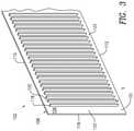
- FIG. 3is a perspective view of an example microstructure panel of the absorbent microstructure array of FIG. 1 .
- FIG. 5is a perspective view of another example microstructure panel comprising capillary ridge walls.
- FIG. 8is a perspective view of an example of an enclosing microstructure panel.
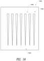
- FIG. 9is a perspective view of an example of an absorbent microstructure array a substantially flat configuration.
- FIG. 11is a perspective view of an example of an absorbent microstructure array having cross notched capillary ridges.
- the present disclosureis directed to absorbent microstructure arrays that can be utilized in a wide variety of products.
- Examples of products that can incorporate the absorbent microstructure arraysinclude, but are not limited to diapers, mops, hygiene, sponges, and towels—just to name a few.
- the absorbent microstructure arrayscan be utilized to uptake and store a fluid.
- the absorbent microstructure arrayscan be used to transport the fluid in one or more embodiments.
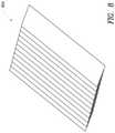
- FIGS. 2 and 3collectively illustrate a close-up perspective view of the microstructure panel 102 that comprises a front surface 106 , a back surface 108 , an upper edge 110 , a lower edge 112 , a right edge 114 , and a left edge 116 .
- the right edge 114 and left edge 116are best illustrated in FIG. 1 .
- the microstructure panel 102is constructed from a base or substrate 101 that is constructed from a solid material such as a polymer, while in other embodiments the substrate 101 can be fabricated from a porous material that allows fluid to be filtered and or transmitted between the pluralities of microstructure panels.
- the microstructure panel 102comprises a plurality of capillary ridges, such as capillary ridges 118 and 120 , which are adjacent to one another.
- the capillary ridgesprotrude or extend from the front surface 106 .
- a spacing S between the capillary ridges 118 and 120defines a width dimension of a capillary tube that is created when the microstructure panels are mated together to form the array 100 .
- the capillary ridgessuch as capillary ridge 118 comprises a height HCR that specifies a distance that the capillary ridge 118 extends away from the front surface 106 .
- the capillary ridge 118also has a width dimension W CR that specifies a distance between opposing sidewalls 124 and 126 of the capillary ridge 118 .
- the capillary ridge 118also comprises a contacting surface 128 that mates with the back surface of an adjacent panel.
- the capillary tube 138would have a substantially elliptical cross section.
- FIG. 5illustrates another microstructure panel 200 that comprises various capillary wall ridges, such as capillary wall ridge 202 that function to restrict fluid flow.
- sections of capillary ridgescan be separated or segmented using capillary wall ridges.
- a first section capillary ridges 204is partially surrounded by a capillary wall ridge 202 .
- the first section capillary ridges 204is disposed adjacent to a second section of capillary ridges 206 that are partially surrounded by a capillary wall ridge 208 .
- a lower area 210 of the capillary ridgesis not enclosed by a capillary wall ridge.
- another microstructure panel 300comprises a capillary wall ridge 302 that extends along a length of an upper edge 304 of the microstructure panel 300 and connects to outermost capillary ridges (such as outermost capillary ridge 306 ) to prevent fluid from being drawn above the capillary wall ridge or outwardly from a left edge or right edge of the plurality of microstructure panels and/or array when assembled into an absorbent microstructure array.
- outermost capillary ridgessuch as outermost capillary ridge 306
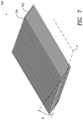
- some embodiments of absorbent microstructure arrayscan be layered in unique manners. For example, in FIG. 7 , each of a plurality of microstructure panels is laid in a feathered or offset pattern to create an absorbent microstructure array 700 .
- adjacent microstructure panelssuch as panel 702 and 704 are set at an angle ⁇ that is measured relative to a reference plane P.
- the reference plane Pis oriented perpendicularly to embodiments where the microstructure panels are vertically oriented such as illustrated in FIGS. 1 and 2 .
- the microstructure panels of the absorbent microstructure array 700are set at approximately 45 degrees (other angles can likewise be utilized). The angling of the microstructure panels allows for the placement and use of the absorbent microstructure array 700 in a location where height is a limiting factor, such as thin materials like diapers or floor mop heads.
- FIG. 10illustrates another example microstructure panel 1000 that comprises capillary ridges with nano-coating 1002 that function to increase the capillary action of the capillary tubes created when a plurality of the microstructure panels 1000 are joined together to create an absorbent microstructure array.
- the nano-coating 1002includes nano-structures such as bumps that enhance capillary action of the plurality of microstructure panels relative to the plurality of microstructure panels with no nano-structure coating.
- FIG. 10only two of the capillary channel surfaces are shown to be coated. Any number of the surfaces could be coated if desired.
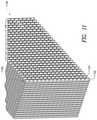
- FIG. 11illustrates another example absorbent microstructure array 1100 having a plurality of microstructure panels such as microstructure panel 1102 that comprises capillary ridges that have cross-cut notches, such as cross-cut notch 1104 .
- the cross-cut notchescreate additional volume for fluid collection. That is, when fluid is drawn into a capillary tube 1106 , the fluid will begin to cross the capillary ridges through the cross-cut notches.
- FIGS. 14 and 15collectively illustrate yet another example absorbent microstructure array 1300 that comprises rows of capillary ridges of varying size and configuration.
- the array 1300is constructed from a plurality of microstructure panels such as microstructure panel 1302 .
- a close up view of section A/A of the microstructure panel 1302is illustrated in FIG. 15 .
- the plurality of capillary ridges of the microstructure panel 1302comprises two rows of capillary ridges.
- a first row 1304 of the two rowscomprise capillary ridges having a first width W 1 and a second row 1306 of the two rows comprise capillary ridges create spaces with a second width W 2 that is different to that of the first width W 1 .
- additional rows of capillary ridgescan be utilized.
- a plurality of capillary ridges rowscan be arranged such that the capillary channels (e.g., space between adjacent capillary ridges) of higher rows of capillary ridges are successively narrower towards a top of the microstructure array.
- FIG. 16illustrates a portion of another example microstructure panel 1400 that comprises a plurality of capillary ridges 1402 that are tapered from a lower edge 1404 to an upper edge 1406 to compensate for forces exerted on the fluid due to gravity. That is, as the space between adjacent capillary ridges narrows, the capillary effect increases, thereby increasing the velocity of the fluid to compensate for the force of gravity.
- a hyphenated term(e.g., “on-demand”) may be occasionally interchangeably used with its non-hyphenated version (e.g., “on demand”)
- a capitalized entrye.g., “Software”
- a non-capitalized versione.g., “software”
- a plural termmay be indicated with or without an apostrophe (e.g., PE's or PEs)
- an italicized terme.g., “N+1” may be interchangeably used with its non-italicized version (e.g., “N+1”).
- Such occasional interchangeable usesshall not be considered inconsistent with each other.
- a “means for”performing a task or set of tasks. It will be understood that a “means for” may be expressed herein in terms of a structure, device, assembly, sub-assembly, component, and combinations thereof. Alternatively, in some embodiments the “means for” is expressed in terms of prose, or as a flow chart or a diagram.
- first, second, etc.may be used herein to describe various elements, components, regions, layers and/or sections, these elements, components, regions, layers and/or sections should not necessarily be limited by such terms. These terms are only used to distinguish one element, component, region, layer or section from another element, component, region, layer or section. Thus, a first element, component, region, layer or section discussed below could be termed a second element, component, region, layer or section without departing from the teachings of the present disclosure.
- Example embodiments of the present disclosureare described herein with reference to illustrations of idealized embodiments (and intermediate structures) of the present disclosure. As such, variations from the shapes of the illustrations as a result, for example, of manufacturing techniques and/or tolerances, are to be expected. Thus, the example embodiments of the present disclosure should not be construed as necessarily limited to the particular shapes of regions illustrated herein, but are to include deviations in shapes that result, for example, from manufacturing.
- Any and/or all elements, as disclosed herein,can be formed from a same, structurally continuous piece, such as being unitary, and/or be separately manufactured and/or connected, such as being an assembly and/or modules. Any and/or all elements, as disclosed herein, can be manufactured via any manufacturing processes, whether additive manufacturing, subtractive manufacturing and/or other any other types of manufacturing. For example, some manufacturing processes include three dimensional (3D) printing, laser cutting, computer numerical control (CNC) routing, milling, pressing, stamping, vacuum forming, hydroforming, injection molding, lithography and/or others.
- 3Dthree dimensional
- CNCcomputer numerical control
- any and/or all elements, as disclosed herein,can include, whether partially and/or fully, a solid, including a metal, a mineral, a ceramic, an amorphous solid, such as glass, a glass ceramic, an organic solid, such as wood and/or a polymer, such as rubber, a composite material, a semiconductor, a nano-material, a biomaterial and/or any combinations thereof.
- a solidincluding a metal, a mineral, a ceramic, an amorphous solid, such as glass, a glass ceramic, an organic solid, such as wood and/or a polymer, such as rubber, a composite material, a semiconductor, a nano-material, a biomaterial and/or any combinations thereof.
- any and/or all elements, as disclosed herein,can include, whether partially and/or fully, a coating, including an informational coating, such as ink, an adhesive coating, a melt-adhesive coating, such as vacuum seal and/or heat seal, a release coating, such as tape liner, a low surface energy coating, an optical coating, such as for tint, color, hue, saturation, tone, shade, transparency, translucency, non-transparency, luminescence, anti-reflection and/or holographic, a photo-sensitive coating, an electronic and/or thermal property coating, such as for passivity, insulation, resistance or conduction, a magnetic coating, a water-resistant and/or waterproof coating, a scent coating and/or any combinations thereof.
- a coatingincluding an informational coating, such as ink, an adhesive coating, a melt-adhesive coating, such as vacuum seal and/or heat seal, a release coating, such as tape liner, a low surface energy coating, an optical coating, such as for tint, color, hue
- relative termssuch as “below,” “lower,” “above,” and “upper” may be used herein to describe one element's relationship to another element as illustrated in the accompanying drawings. Such relative terms are intended to encompass different orientations of illustrated technologies in addition to the orientation depicted in the accompanying drawings. For example, if a device in the accompanying drawings is turned over, then the elements described as being on the “lower” side of other elements would then be oriented on “upper” sides of the other elements. Similarly, if the device in one of the figures is turned over, elements described as “below” or “beneath” other elements would then be oriented “above” the other elements. Therefore, the example terms “below” and “lower” can, therefore, encompass both an orientation of above and below.
Landscapes
- Health & Medical Sciences (AREA)
- Epidemiology (AREA)
- Engineering & Computer Science (AREA)
- Biomedical Technology (AREA)
- Heart & Thoracic Surgery (AREA)
- Vascular Medicine (AREA)
- Life Sciences & Earth Sciences (AREA)
- Animal Behavior & Ethology (AREA)
- General Health & Medical Sciences (AREA)
- Public Health (AREA)
- Veterinary Medicine (AREA)
- Absorbent Articles And Supports Therefor (AREA)
Abstract
Description
Claims (13)
Priority Applications (1)
| Application Number | Priority Date | Filing Date | Title |
|---|---|---|---|
| US16/600,522US11254085B2 (en) | 2015-08-19 | 2019-10-13 | Absorbent microstructure arrays and methods of use |
Applications Claiming Priority (3)
| Application Number | Priority Date | Filing Date | Title |
|---|---|---|---|
| US201562283051P | 2015-08-19 | 2015-08-19 | |
| US15/233,701US10479046B2 (en) | 2015-08-19 | 2016-08-10 | Absorbent microstructure arrays and methods of use |
| US16/600,522US11254085B2 (en) | 2015-08-19 | 2019-10-13 | Absorbent microstructure arrays and methods of use |
Related Parent Applications (1)
| Application Number | Title | Priority Date | Filing Date |
|---|---|---|---|
| US15/233,701ContinuationUS10479046B2 (en) | 2015-08-19 | 2016-08-10 | Absorbent microstructure arrays and methods of use |
Publications (2)
| Publication Number | Publication Date |
|---|---|
| US20200039175A1 US20200039175A1 (en) | 2020-02-06 |
| US11254085B2true US11254085B2 (en) | 2022-02-22 |
Family
ID=58157385
Family Applications (2)
| Application Number | Title | Priority Date | Filing Date |
|---|---|---|---|
| US15/233,701Active2036-12-18US10479046B2 (en) | 2015-08-19 | 2016-08-10 | Absorbent microstructure arrays and methods of use |
| US16/600,522ActiveUS11254085B2 (en) | 2015-08-19 | 2019-10-13 | Absorbent microstructure arrays and methods of use |
Family Applications Before (1)
| Application Number | Title | Priority Date | Filing Date |
|---|---|---|---|
| US15/233,701Active2036-12-18US10479046B2 (en) | 2015-08-19 | 2016-08-10 | Absorbent microstructure arrays and methods of use |
Country Status (1)
| Country | Link |
|---|---|
| US (2) | US10479046B2 (en) |
Families Citing this family (8)
| Publication number | Priority date | Publication date | Assignee | Title |
|---|---|---|---|---|
| US10040018B2 (en) | 2013-01-09 | 2018-08-07 | Imagine Tf, Llc | Fluid filters and methods of use |
| US10730047B2 (en) | 2014-06-24 | 2020-08-04 | Imagine Tf, Llc | Micro-channel fluid filters and methods of use |
| US10124275B2 (en) | 2014-09-05 | 2018-11-13 | Imagine Tf, Llc | Microstructure separation filters |
| US10118842B2 (en) | 2015-07-09 | 2018-11-06 | Imagine Tf, Llc | Deionizing fluid filter devices and methods of use |
| WO2019162518A1 (en)* | 2018-02-26 | 2019-08-29 | T&W Engineering A/S | Electrode for detecting bioelectrical signals |
| WO2020086633A1 (en)* | 2018-10-23 | 2020-04-30 | Imagine Tf, Llc | Filter panel with macro, micro and nano structures |
| US20200298156A1 (en)* | 2019-03-20 | 2020-09-24 | Imagine Tf, Llc | Layered panels with structures for separation |
| US12060261B2 (en)* | 2019-11-06 | 2024-08-13 | Bvw Holding Ag | Extremal microstructured surfaces |
Citations (6)
| Publication number | Priority date | Publication date | Assignee | Title |
|---|---|---|---|---|
| US4410427A (en)* | 1981-11-02 | 1983-10-18 | Donaldson Company, Inc. | Fluid filtering device |
| US20030104170A1 (en)* | 2001-02-07 | 2003-06-05 | 3M Innovative Properties Company | Microstructured surface film assembly for liquid acquisition and transport |
| US20060163150A1 (en)* | 2002-07-10 | 2006-07-27 | Dondaldson Company, Inc. | Fluted filter medium and process for its manufacture |
| US8357219B2 (en)* | 2005-10-11 | 2013-01-22 | Donaldson Company, Inc. | Air filter arrangement; assembly and methods |
| US20140224658A1 (en)* | 2013-01-09 | 2014-08-14 | Imagine Tf, Llc | Fluid filters and methods of use |
| US20150336360A1 (en)* | 2008-08-01 | 2015-11-26 | Ohio State Innovation Foundation | Hierarchical structures for superhydrophobic surfaces and methods of making |
Family Cites Families (127)
| Publication number | Priority date | Publication date | Assignee | Title |
|---|---|---|---|---|
| US1977174A (en) | 1933-10-19 | 1934-10-16 | Victor R Heftler | Filter |
| SE316422B (en) | 1964-04-14 | 1969-10-20 | Ceskoslovenska Akademie Ved | |
| US3250396A (en) | 1964-08-12 | 1966-05-10 | Ametek Inc | Rotary disc filter |
| US3948779A (en) | 1972-12-29 | 1976-04-06 | Jackson Clifford E | Disc filter |
| US3884805A (en) | 1974-05-13 | 1975-05-20 | Artisan Ind | Apparatus and process for continuous concentration of solids from a solids-containing fluid |
| US4668558A (en) | 1978-07-20 | 1987-05-26 | Minnesota Mining And Manufacturing Company | Shaped plastic articles having replicated microstructure surfaces |
| US4267045A (en) | 1978-10-26 | 1981-05-12 | The Babcock & Wilcox Company | Labyrinth disk stack having disks with integral filter screens |
| EP0057670B1 (en) | 1981-02-04 | 1986-09-03 | Charles Doucet | Disc filter for liquids |
| US4410430A (en) | 1981-05-11 | 1983-10-18 | California Institute Of Technology | Stacked-disc structure for fluid filter or valve silencer |
| US4423090A (en) | 1982-02-02 | 1983-12-27 | General Motors Corporation | Method of making wall-flow monolith filter |
| JPS58137452A (en) | 1982-02-08 | 1983-08-15 | Nippon Soken Inc | Filtering body for electrostatic filter apparatus |
| US4601861A (en) | 1982-09-30 | 1986-07-22 | Amerace Corporation | Methods and apparatus for embossing a precision optical pattern in a resinous sheet or laminate |
| US4478769A (en) | 1982-09-30 | 1984-10-23 | Amerace Corporation | Method for forming an embossing tool with an optically precise pattern |
| US4486363A (en) | 1982-09-30 | 1984-12-04 | Amerace Corporation | Method and apparatus for embossing a precision optical pattern in a resinous sheet |
| GB2191110B (en) | 1986-06-06 | 1989-12-06 | Plessey Co Plc | Chromatographic separation device |
| US4797175A (en) | 1987-03-09 | 1989-01-10 | Hughes Aircraft Company | Method for making solid element fluid filter for removing small particles from fluids |
| US4902420A (en) | 1987-03-27 | 1990-02-20 | Pall Corporation | Segmented filter disc with slotted support and drainage plate and support spacer |
| US5100551A (en) | 1987-03-27 | 1992-03-31 | Pall Corporation | Segmented filter disc with slotted support and drainage plate |
| US4842794A (en) | 1987-07-30 | 1989-06-27 | Applied Extrusion Technologies, Inc. | Method of making apertured films and net like fabrics |
| US4842739A (en) | 1987-08-20 | 1989-06-27 | Minnesota Mining And Manufacturing Company | High surface area filter cartridge |
| DE3818281A1 (en) | 1988-03-10 | 1989-09-21 | Schwaebische Huettenwerke Gmbh | EXHAUST FILTER |
| DE3828347A1 (en) | 1988-08-20 | 1990-03-01 | Schwaebische Huettenwerke Gmbh | EXHAUST GAS FILTER FOR HEATING OR COMBUSTION PLANTS |
| US4960449A (en) | 1989-02-28 | 1990-10-02 | Cummins Engine Company, Inc. | Ceramic particulate trap and method of making the same |
| DE4004079A1 (en) | 1990-02-08 | 1991-08-14 | Lippold Hans Joachim | FILTER INSERT |
| US5200073A (en) | 1991-02-22 | 1993-04-06 | Gelman Sciences Inc. | Polymeric film filter assembly |
| US5207962A (en) | 1991-06-25 | 1993-05-04 | Applied Extrusion Technologies, Inc. | Method of making apertured film fabrics |
| US5262107A (en) | 1991-06-25 | 1993-11-16 | Applied Extrusion Technologies, Inc. | Method of making apertured film fabrics |
| US5204690A (en) | 1991-07-01 | 1993-04-20 | Xerox Corporation | Ink jet printhead having intergral silicon filter |
| DE4206738A1 (en) | 1992-03-04 | 1993-09-09 | Minnesota Mining & Mfg | FILTER ELEMENT FOR FILTERING FLUIDS, IN PARTICULAR FOR FILTERING AIR |
| WO1993022053A1 (en) | 1992-05-01 | 1993-11-11 | Trustees Of The University Of Pennsylvania | Microfabricated detection structures |
| US5404890A (en) | 1993-06-11 | 1995-04-11 | R. J. Reynolds Tobacco Company | Cigarette filter |
| US5985164A (en) | 1994-03-07 | 1999-11-16 | Regents Of The University Of California | Method for forming a filter |
| US5645704A (en) | 1994-05-03 | 1997-07-08 | Eugene Sandler | Electrostatic filter device |
| US5552046A (en) | 1995-01-23 | 1996-09-03 | Johnston; Arthur W. | Multi-stage microbiological water filter |
| GB9623185D0 (en) | 1996-11-09 | 1997-01-08 | Epigem Limited | Improved micro relief element and preparation thereof |
| US6524488B1 (en) | 1998-06-18 | 2003-02-25 | 3M Innovative Properties Company | Method of filtering certain particles from a fluid using a depth loading filtration media |
| US6375871B1 (en) | 1998-06-18 | 2002-04-23 | 3M Innovative Properties Company | Methods of manufacturing microfluidic articles |
| GB9718858D0 (en) | 1997-09-06 | 1997-11-12 | Harlent Limited | Filter Cartridges and Filter Cells |
| DE19742439C1 (en) | 1997-09-26 | 1998-10-22 | Boehringer Ingelheim Int | Fluid micro-filter |
| JP2001520377A (en) | 1997-10-15 | 2001-10-30 | アクレイラ バイオサイエンシズ,インコーポレイティド | Laminated micro structural device and method of manufacturing laminated micro structural device |
| EP1003078A3 (en) | 1998-11-17 | 2001-11-07 | Corning Incorporated | Replicating a nanoscale pattern |
| US6280824B1 (en) | 1999-01-29 | 2001-08-28 | 3M Innovative Properties Company | Contoured layer channel flow filtration media |
| US6915566B2 (en) | 1999-03-01 | 2005-07-12 | Texas Instruments Incorporated | Method of fabricating flexible circuits for integrated circuit interconnections |
| US6274035B1 (en) | 1999-03-23 | 2001-08-14 | Sidney W. K. Yuan | Biological filtration using parallel sheets |
| US6346192B2 (en) | 1999-05-14 | 2002-02-12 | Therox, Inc. | Apparatus for high pressure fluid filtration |
| DE19925926A1 (en) | 1999-06-08 | 2000-12-14 | Bayer Ag | Catalysts based on titanium-containing, organic-inorganic hybrid materials for the selective oxidation of hydrocarbons |
| AU762646B2 (en) | 1999-06-18 | 2003-07-03 | Itec Initiatives | Filtration disc including electric field formation |
| EP1449585B1 (en) | 1999-07-07 | 2007-09-12 | 3M Innovative Properties Company | Microfluidic article |
| US7223364B1 (en) | 1999-07-07 | 2007-05-29 | 3M Innovative Properties Company | Detection article having fluid control film |
| US9267023B2 (en) | 1999-08-04 | 2016-02-23 | Hybrid Plastics, Inc. | Method for modifying surface properties with nanostructured chemicals |
| US6273938B1 (en)* | 1999-08-13 | 2001-08-14 | 3M Innovative Properties Company | Channel flow filter |
| US6454839B1 (en) | 1999-10-19 | 2002-09-24 | 3M Innovative Properties Company | Electrofiltration apparatus |
| US6632357B1 (en) | 1999-11-18 | 2003-10-14 | University Of South Florida | Reverse osmosis (“RO”) membrane system incorporating function of flow channel spacer |
| ATE354430T1 (en) | 1999-12-08 | 2007-03-15 | Baxter Int | METHOD FOR PRODUCING A MICROPOROUS FILTER MEMBRANE |
| US6877349B2 (en) | 2000-08-17 | 2005-04-12 | Industrial Origami, Llc | Method for precision bending of sheet of materials, slit sheets fabrication process |
| AU9076901A (en) | 2000-09-15 | 2002-03-26 | Cuno Inc | Spiral pleated filter cartridges |
| ATE345860T1 (en) | 2000-09-21 | 2006-12-15 | Lpd Technologies Inc | FLUID FILTER ELEMENT |
| DE60028973T2 (en) | 2000-10-11 | 2007-02-15 | 3M Innovative Properties Co., Saint Paul | Combination filter system with filter medium with flow channel and adsorption particle filter medium |
| NL1016779C2 (en) | 2000-12-02 | 2002-06-04 | Cornelis Johannes Maria V Rijn | Mold, method for manufacturing precision products with the aid of a mold, as well as precision products, in particular microsieves and membrane filters, manufactured with such a mold. |
| AU2002251946A1 (en) | 2001-02-14 | 2002-08-28 | Science And Technology Corporation @ Unm | Nanostructured devices for separation and analysis |
| US6605215B2 (en) | 2001-03-20 | 2003-08-12 | Norbert Assion | Hybrid spin-on filter |
| US6418968B1 (en) | 2001-04-20 | 2002-07-16 | Nanostream, Inc. | Porous microfluidic valves |
| US6824581B1 (en) | 2001-05-01 | 2004-11-30 | Dana Corporation | Pleated filter media with embossed spacers and cross flow |
| DE60237490D1 (en) | 2001-05-01 | 2010-10-14 | Wix Filtration Corp Llc | Folded filter medium with impressed spacers and for cross flow |
| WO2002100551A1 (en) | 2001-06-11 | 2002-12-19 | Rochester Institute Of Technology | An electrostatic filter and a method thereof |
| WO2004054793A1 (en) | 2002-12-13 | 2004-07-01 | Ole-Bendt Rasmussen | Laminates of films having improved resistance to bending in all directions and methods and apparatus for their manufacture |
| US6589317B2 (en) | 2001-08-10 | 2003-07-08 | 3M Innovative Properties Company | Structured surface filtration media array |
| WO2003047722A2 (en) | 2001-12-03 | 2003-06-12 | Donaldson Company, Inc. | Filter element using corrugated media sheet |
| US7238255B2 (en) | 2001-12-31 | 2007-07-03 | Gyros Patent Ab | Microfluidic device and its manufacture |
| ITGE20020023A1 (en) | 2002-03-15 | 2003-09-15 | Alfatech S P A | CHROMATOGRAPHIC APPARATUS |
| CA2482566C (en) | 2002-04-16 | 2010-07-20 | Princeton University | Gradient structures interfacing microfluidics and nanofluidics, methods for fabrication and uses thereof |
| SE0201738D0 (en) | 2002-06-07 | 2002-06-07 | Aamic Ab | Micro-fluid structures |
| US6746890B2 (en) | 2002-07-17 | 2004-06-08 | Tini Alloy Company | Three dimensional thin film devices and methods of fabrication |
| US6936086B2 (en) | 2002-09-11 | 2005-08-30 | Planar Systems, Inc. | High conductivity particle filter |
| CA2500392C (en) | 2002-09-27 | 2012-11-27 | The General Hospital Corporation | Microfluidic device for cell separation and uses thereof |
| AU2003299553A1 (en) | 2002-10-23 | 2004-05-13 | The Trustees Of Princeton University | Method for continuous particle separation using obstacle arrays asymmetrically aligned to fields |
| US7081208B2 (en) | 2002-12-16 | 2006-07-25 | International Business Machines Corporation | Method to build a microfilter |
| EP1583657A1 (en) | 2003-01-06 | 2005-10-12 | Avery Dennison Corporation | Embossed oriented optical films |
| FI20030919A7 (en) | 2003-06-19 | 2004-12-20 | Avantone Oy | Method and apparatus for manufacturing an electronic thin film component and electronic thin film component |
| US8241543B2 (en) | 2003-08-07 | 2012-08-14 | The Procter & Gamble Company | Method and apparatus for making an apertured web |
| US7104406B2 (en) | 2003-08-18 | 2006-09-12 | Industrial Technology Research Institute | Micro-filter for filtering blood cells |
| US7282148B2 (en) | 2003-10-30 | 2007-10-16 | International Business Machines Corporation | Porous silicon composite structure as large filtration array |
| US20060219627A1 (en) | 2005-03-31 | 2006-10-05 | Rodgers M S | MEMS filter module with concentric filtering walls |
| US7425227B1 (en) | 2004-06-17 | 2008-09-16 | Wix Filtration Corp Llc | Pleated filter element with offset emboss pattern |
| US7959780B2 (en) | 2004-07-26 | 2011-06-14 | Emporia Capital Funding Llc | Textured ion exchange membranes |
| US7323105B1 (en) | 2004-08-11 | 2008-01-29 | Fleetguard, Inc. | High capacity direct flow filter with maintained channel width |
| US7955504B1 (en) | 2004-10-06 | 2011-06-07 | State Of Oregon Acting By And Through The State Board Of Higher Education On Behalf Of Oregon State University | Microfluidic devices, particularly filtration devices comprising polymeric membranes, and method for their manufacture and use |
| US7163733B2 (en) | 2004-11-12 | 2007-01-16 | Eastman Kodak Company | Touch screen having spacer dots with channels |
| CN101137908B (en) | 2005-03-07 | 2012-07-04 | 可乐丽股份有限公司 | Microchannel array, manufacturing method thereof, and blood measurement method using same |
| WO2006119252A2 (en) | 2005-04-29 | 2006-11-09 | University Of Rochester | Ultrathin nanoscale membranes, methods of making, and uses thereof |
| DE602006012307D1 (en) | 2005-05-20 | 2010-04-01 | Aquaporin Aps | MEMBRANE FOR FILTRATION OF WATER |
| US7211232B1 (en) | 2005-11-07 | 2007-05-01 | Geo2 Technologies, Inc. | Refractory exhaust filtering method and apparatus |
| US20070151920A1 (en) | 2005-12-06 | 2007-07-05 | Kay Ronald J | System and method of micromolded filtration microstructure and devices |
| EP1847174A3 (en) | 2006-04-13 | 2008-05-21 | Newa Tecno Industria S.R.L. | Aquarium filter |
| WO2007143133A2 (en) | 2006-05-31 | 2007-12-13 | Micropore Plastics, Inc. | Modular filter assembly |
| US9134471B2 (en) | 2006-06-28 | 2015-09-15 | 3M Innovative Properties Company | Oriented polymeric articles and method |
| US7588619B2 (en) | 2006-11-28 | 2009-09-15 | Wix Filtration Corp. | Cross-flow filter media and filter assembly |
| GB2446204A (en) | 2007-01-12 | 2008-08-06 | Univ Brunel | A Microfluidic device |
| CN101765762B (en) | 2007-04-16 | 2013-08-14 | 通用医疗公司以马萨诸塞州通用医疗公司名义经营 | Systems and methods for aggregating particles in microchannels |
| CN201094877Y (en) | 2007-08-17 | 2008-08-06 | 简焕然 | Wedge-shaped filter element structure |
| KR101720919B1 (en) | 2008-02-28 | 2017-03-28 | 쓰리엠 이노베이티브 프로퍼티즈 컴파니 | Touch screen sensor |
| WO2009111461A2 (en) | 2008-03-04 | 2009-09-11 | University Of Utah Research Foundation | Microfluidic flow cell |
| JP2011519310A (en) | 2008-04-28 | 2011-07-07 | コーニング インコーポレイテッド | Monolith diaphragm module for filtering liquids |
| JP2010115624A (en) | 2008-11-14 | 2010-05-27 | Fuji Xerox Co Ltd | Microchannel device, separation device, and separation method |
| CN102300802A (en) | 2008-12-17 | 2011-12-28 | 3M创新有限公司 | Fabrication Of Conductive Nanostructures On A Flexible Substrate |
| EP2421628A4 (en) | 2009-04-23 | 2012-10-10 | Logos Energy Inc | Lateral displacement array for microfiltration |
| EP2430652B1 (en) | 2009-05-12 | 2019-11-20 | The Board of Trustees of the University of Illionis | Printed assemblies of ultrathin, microscale inorganic light emitting diodes for deformable and semitransparent displays |
| DE102009040202B4 (en) | 2009-09-07 | 2015-10-01 | Mann + Hummel Gmbh | filter |
| TR201811087T4 (en) | 2009-10-19 | 2018-08-27 | Lpd Tech Inc | Embossed fluid filter element. |
| US8307994B2 (en) | 2009-10-28 | 2012-11-13 | International Business Machines Corporation | Surface charge enabled nanoporous semi-permeable membrane for desalination |
| WO2011066055A2 (en) | 2009-11-24 | 2011-06-03 | Unipixel Displays, Inc. | Formation of electrically conductive pattern by surface energy modification |
| CA2688470A1 (en) | 2009-12-11 | 2011-06-11 | Allan Manninen | Industrial fabric comprised of selectively slit and embossed film |
| TWI506070B (en) | 2009-12-14 | 2015-11-01 | 3M Innovative Properties Co | Microperforated polymeric film and methods of making and using the same |
| US8297449B2 (en) | 2010-01-12 | 2012-10-30 | International Business Machines Corporation | Nanoporous semi-permeable membrane and methods for fabricating the same |
| SE535177C2 (en) | 2010-04-14 | 2012-05-08 | Nanospace Ab | Micromechanical filters |
| JP2014522294A (en) | 2011-04-13 | 2014-09-04 | ジーエフディー ファブリックス,インク. | Filter elements for fluid filtration systems |
| US9957472B2 (en) | 2011-09-22 | 2018-05-01 | Georgia Tech Research Corporation | Deterministic high-density single-cell trap array |
| SG11201505411RA (en) | 2013-01-24 | 2015-08-28 | Univ Singapore | Microdevices for separation of non-spherical particles and applications thereof |
| CN203139755U (en) | 2013-03-22 | 2013-08-21 | 新疆泓科节水设备制造有限公司 | Laminated-type water filter for micro-irrigation |
| CN106029202B (en) | 2014-01-07 | 2019-01-08 | 想象Tf有限责任公司 | Fluid filter and application method |
| JP2017529235A (en) | 2014-06-24 | 2017-10-05 | イマジン ティーエフ,エルエルシー | Microchannel fluid filter and method of using the same |
| US10730047B2 (en) | 2014-06-24 | 2020-08-04 | Imagine Tf, Llc | Micro-channel fluid filters and methods of use |
| US10124275B2 (en) | 2014-09-05 | 2018-11-13 | Imagine Tf, Llc | Microstructure separation filters |
| JP6509330B2 (en) | 2014-09-05 | 2019-05-08 | イマジン ティーエフ,エルエルシー | Fine structure separation filter |
| WO2016133929A1 (en) | 2015-02-18 | 2016-08-25 | Imagine Tf, Llc | Three dimensional filter devices and apparatuses |
| US10118842B2 (en) | 2015-07-09 | 2018-11-06 | Imagine Tf, Llc | Deionizing fluid filter devices and methods of use |
| WO2017007734A1 (en) | 2015-07-09 | 2017-01-12 | Imagine Tf, Llc | Deionizing fluid filter devices and methods of use |
- 2016
- 2016-08-10USUS15/233,701patent/US10479046B2/enactiveActive
- 2019
- 2019-10-13USUS16/600,522patent/US11254085B2/enactiveActive
Patent Citations (6)
| Publication number | Priority date | Publication date | Assignee | Title |
|---|---|---|---|---|
| US4410427A (en)* | 1981-11-02 | 1983-10-18 | Donaldson Company, Inc. | Fluid filtering device |
| US20030104170A1 (en)* | 2001-02-07 | 2003-06-05 | 3M Innovative Properties Company | Microstructured surface film assembly for liquid acquisition and transport |
| US20060163150A1 (en)* | 2002-07-10 | 2006-07-27 | Dondaldson Company, Inc. | Fluted filter medium and process for its manufacture |
| US8357219B2 (en)* | 2005-10-11 | 2013-01-22 | Donaldson Company, Inc. | Air filter arrangement; assembly and methods |
| US20150336360A1 (en)* | 2008-08-01 | 2015-11-26 | Ohio State Innovation Foundation | Hierarchical structures for superhydrophobic surfaces and methods of making |
| US20140224658A1 (en)* | 2013-01-09 | 2014-08-14 | Imagine Tf, Llc | Fluid filters and methods of use |
Also Published As
| Publication number | Publication date |
|---|---|
| US20200039175A1 (en) | 2020-02-06 |
| US10479046B2 (en) | 2019-11-19 |
| US20170050407A1 (en) | 2017-02-23 |
Similar Documents
| Publication | Publication Date | Title |
|---|---|---|
| US11254085B2 (en) | Absorbent microstructure arrays and methods of use | |
| US10758849B2 (en) | Three dimensional filter devices and apparatuses | |
| WO2014014051A1 (en) | Fiber reinforced composite material structure and composite material molding using same as well as manufacturing method therefor | |
| CN113725514A (en) | flexible display device | |
| CN107734840B (en) | Liquid-cooled cooling structure based on printed circuit board three-dimensional microchannel array | |
| CN101266109A (en) | Total heat exchanger and manufacturing method thereof | |
| US10337765B2 (en) | Solar cell module | |
| CN212232002U (en) | High-heat-conduction bending-resistant heat dissipation film | |
| CN108110071A (en) | Photovoltaic module, photovoltaic device and preparation method of photovoltaic module | |
| EP4023997A1 (en) | Heat exchange plate and heat exchanger containing same | |
| CN106558766A (en) | Metamaterial composite structure and its manufacture method and antenna house | |
| KR102290125B1 (en) | Backing Elements for Solar Modules | |
| CN102810761B (en) | The manufacture method of sandwich Meta Materials and manufacture method and sandwich metamaterial antenna cover | |
| WO2014115868A1 (en) | Sound-absorbing structure and sound-absorbing-structured laminate | |
| KR102716018B1 (en) | Heater for liquid and manufacturing method thereof | |
| CN112105247A (en) | Electromagnetic shielding film | |
| JPWO2015159665A1 (en) | Carbon-coated planar heater and method for manufacturing the same | |
| US8581156B2 (en) | Apparatus with heating part | |
| JP2003130571A (en) | Stacked heat exchanger | |
| CN107251293A (en) | Fuel cell system | |
| CN207427569U (en) | One kind is based on the cold cooling structure of printed circuit board three-dimensional micro-channel array liquid | |
| CN102637959A (en) | Metamaterial with dielectric substrate with nonuniform thickness | |
| CN115335655A (en) | Heat transfer plate and heat exchange element | |
| TWM472181U (en) | Heat-spreading board structure | |
| JP2014163571A (en) | Heat exchange element |
Legal Events
| Date | Code | Title | Description |
|---|---|---|---|
| AS | Assignment | Owner name:IMAGINE TF, LLC, CALIFORNIA Free format text:ASSIGNMENT OF ASSIGNORS INTEREST;ASSIGNOR:RICHARDSON, BRIAN EDWARD;REEL/FRAME:050694/0702 Effective date:20160810 | |
| FEPP | Fee payment procedure | Free format text:ENTITY STATUS SET TO UNDISCOUNTED (ORIGINAL EVENT CODE: BIG.); ENTITY STATUS OF PATENT OWNER: SMALL ENTITY | |
| FEPP | Fee payment procedure | Free format text:ENTITY STATUS SET TO SMALL (ORIGINAL EVENT CODE: SMAL); ENTITY STATUS OF PATENT OWNER: SMALL ENTITY | |
| STPP | Information on status: patent application and granting procedure in general | Free format text:DOCKETED NEW CASE - READY FOR EXAMINATION | |
| STPP | Information on status: patent application and granting procedure in general | Free format text:NON FINAL ACTION MAILED | |
| STPP | Information on status: patent application and granting procedure in general | Free format text:RESPONSE TO NON-FINAL OFFICE ACTION ENTERED AND FORWARDED TO EXAMINER | |
| STPP | Information on status: patent application and granting procedure in general | Free format text:FINAL REJECTION MAILED | |
| STPP | Information on status: patent application and granting procedure in general | Free format text:RESPONSE AFTER FINAL ACTION FORWARDED TO EXAMINER | |
| STPP | Information on status: patent application and granting procedure in general | Free format text:ADVISORY ACTION MAILED | |
| STPP | Information on status: patent application and granting procedure in general | Free format text:DOCKETED NEW CASE - READY FOR EXAMINATION | |
| STPP | Information on status: patent application and granting procedure in general | Free format text:NON FINAL ACTION MAILED | |
| STPP | Information on status: patent application and granting procedure in general | Free format text:RESPONSE TO NON-FINAL OFFICE ACTION ENTERED AND FORWARDED TO EXAMINER | |
| STPP | Information on status: patent application and granting procedure in general | Free format text:NOTICE OF ALLOWANCE MAILED -- APPLICATION RECEIVED IN OFFICE OF PUBLICATIONS | |
| STCF | Information on status: patent grant | Free format text:PATENTED CASE |