US11251189B2 - Gate fringing effect based channel formation for semiconductor device - Google Patents
Gate fringing effect based channel formation for semiconductor deviceDownload PDFInfo
- Publication number
- US11251189B2 US11251189B2US16/380,209US201916380209AUS11251189B2US 11251189 B2US11251189 B2US 11251189B2US 201916380209 AUS201916380209 AUS 201916380209AUS 11251189 B2US11251189 B2US 11251189B2
- Authority
- US
- United States
- Prior art keywords
- memory transistor
- transistor
- memory
- channel
- width
- Prior art date
- Legal status (The legal status is an assumption and is not a legal conclusion. Google has not performed a legal analysis and makes no representation as to the accuracy of the status listed.)
- Active
Links
Images


Classifications
- H01L27/11524—
- H01L27/11521—
- H01L27/11568—
- H01L27/1157—
- H01L29/40117—
- H01L29/4234—
- H01L29/66825—
- H01L29/66833—
- H01L29/7881—
- H01L29/792—
- H—ELECTRICITY
- H10—SEMICONDUCTOR DEVICES; ELECTRIC SOLID-STATE DEVICES NOT OTHERWISE PROVIDED FOR
- H10B—ELECTRONIC MEMORY DEVICES
- H10B41/00—Electrically erasable-and-programmable ROM [EEPROM] devices comprising floating gates
- H10B41/30—Electrically erasable-and-programmable ROM [EEPROM] devices comprising floating gates characterised by the memory core region
- H10B41/35—Electrically erasable-and-programmable ROM [EEPROM] devices comprising floating gates characterised by the memory core region with a cell select transistor, e.g. NAND
- H—ELECTRICITY
- H10—SEMICONDUCTOR DEVICES; ELECTRIC SOLID-STATE DEVICES NOT OTHERWISE PROVIDED FOR
- H10B—ELECTRONIC MEMORY DEVICES
- H10B43/00—EEPROM devices comprising charge-trapping gate insulators
- H10B43/30—EEPROM devices comprising charge-trapping gate insulators characterised by the memory core region
- H10B43/35—EEPROM devices comprising charge-trapping gate insulators characterised by the memory core region with cell select transistors, e.g. NAND
- H—ELECTRICITY
- H10—SEMICONDUCTOR DEVICES; ELECTRIC SOLID-STATE DEVICES NOT OTHERWISE PROVIDED FOR
- H10D—INORGANIC ELECTRIC SEMICONDUCTOR DEVICES
- H10D30/00—Field-effect transistors [FET]
- H10D30/01—Manufacture or treatment
- H10D30/021—Manufacture or treatment of FETs having insulated gates [IGFET]
- H10D30/0411—Manufacture or treatment of FETs having insulated gates [IGFET] of FETs having floating gates
- H—ELECTRICITY
- H10—SEMICONDUCTOR DEVICES; ELECTRIC SOLID-STATE DEVICES NOT OTHERWISE PROVIDED FOR
- H10D—INORGANIC ELECTRIC SEMICONDUCTOR DEVICES
- H10D30/00—Field-effect transistors [FET]
- H10D30/01—Manufacture or treatment
- H10D30/021—Manufacture or treatment of FETs having insulated gates [IGFET]
- H10D30/0413—Manufacture or treatment of FETs having insulated gates [IGFET] of FETs having charge-trapping gate insulators, e.g. MNOS transistors
- H—ELECTRICITY
- H10—SEMICONDUCTOR DEVICES; ELECTRIC SOLID-STATE DEVICES NOT OTHERWISE PROVIDED FOR
- H10D—INORGANIC ELECTRIC SEMICONDUCTOR DEVICES
- H10D30/00—Field-effect transistors [FET]
- H10D30/60—Insulated-gate field-effect transistors [IGFET]
- H10D30/68—Floating-gate IGFETs
- H10D30/681—Floating-gate IGFETs having only two programming levels
- H—ELECTRICITY
- H10—SEMICONDUCTOR DEVICES; ELECTRIC SOLID-STATE DEVICES NOT OTHERWISE PROVIDED FOR
- H10D—INORGANIC ELECTRIC SEMICONDUCTOR DEVICES
- H10D30/00—Field-effect transistors [FET]
- H10D30/60—Insulated-gate field-effect transistors [IGFET]
- H10D30/69—IGFETs having charge trapping gate insulators, e.g. MNOS transistors
- H10D30/694—IGFETs having charge trapping gate insulators, e.g. MNOS transistors characterised by the shapes, relative sizes or dispositions of the gate electrodes
- H—ELECTRICITY
- H10—SEMICONDUCTOR DEVICES; ELECTRIC SOLID-STATE DEVICES NOT OTHERWISE PROVIDED FOR
- H10D—INORGANIC ELECTRIC SEMICONDUCTOR DEVICES
- H10D64/00—Electrodes of devices having potential barriers
- H10D64/01—Manufacture or treatment
- H10D64/031—Manufacture or treatment of data-storage electrodes
- H10D64/037—Manufacture or treatment of data-storage electrodes comprising charge-trapping insulators
Definitions
- This disclosurerelates generally to technical fields of semiconductor manufacturing.
- a conventional NAND flash memory device 100includes multiple NAND strings of memory transistors.
- FIG. 1illustrates two NAND strings of the conventional NAND flash memory device 100 .
- a selected bitline 1is grounded by passing a bitline select voltage 104 of 0 volt through the drain of a drain select (DS) transistor 1 to a node of the memory transistor 102 , while a bitline 2 and the rest of the bitlines are self boosted by coupling to a programming voltage 118 and/or a pass voltage 120 to inhibit the programming.
- a drain select (DS) line 108 and a source select (SS) line 110are coupled to a node of a DS voltage 112 and to a node of a SS voltage 114 , respectively.
- the supply voltage of the DS line 108turns on the DS transistor 1 and maintains the connection of the bitline 1 to the bitline select voltage 104 , but it turns off the DS transistor 2 , thus disconnecting the bitline 2 from the bitline unselect voltage 106 .
- the SS voltage 114 coupled to the SS line 110turns off both the SS transistor 1 and the SS transistor 2 , thus isolating the two bitlines from a node of a common source voltage 116 during the programming.
- a wordline N coupled to the control gate of the memory transistor 102is applied by the programming voltage 118 of 18 volts while the unselected wordlines are applied by the pass voltage 120 of 11 volts. Since the channel of the bitline 1 is coupled to the bitline select voltage 104 of 0 volt, it is maintained at the channel voltage of 0 volt, whereas the channel potential of the bitline 2 is coupled up by the programming voltage 118 and/or the pass voltage 120 . For example, with the pass voltage 120 of 11 volts being supplied to the unselected wordlines, the channel voltage of the bitline 2 may range between 6 to 9 volts.
- the threshold voltage of the cell 102is about ⁇ 2 volt.
- the high voltage of the programming voltage 118causes the tunneling of electrons from the silicon substrate of the memory transistor 102 to the charge trap layer of the memory transistor 102 , thus increasing the threshold voltage to a positive voltage of 1 volt, whereas the voltage differential between the silicon substrate and the floating gate of each unselected cell is not large enough to cause the change in the threshold voltage of its respective transistor.
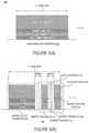
- FIG. 2illustrates an exploded view of a portion of the bitline 2 viewed across Y-direction which includes the SS transistor 2 , a memory transistor 122 (e.g., coupled to an edge wordline, such as the wordline N), and a memory transistor 124 .
- the SS transistor 2controls the bitline 2 for connecting to a common source 202 .
- the SS transistor 2is 200 nm in size, the transistors 90 nm in size, and the channels 100 nm in size.
- the boosted junction potential between the SS transistor 2 and the memory transistor 122may range between 6 and 9 volts, where the gate of the SS transistor 2 is grounded.
- the channel voltage for unselected bitline 2being 6 to 9 volts
- the gate voltage of the memory transistor 122being 18 volts
- the gate voltage of the SS transistor 2being 0 volt
- EHPelectron hole pair
- GDILgate induced drain junction leakage
- the GIDL currentarises in a high electric field under a gate-junction overlap region and a low gate to drain bias.
- the GIDL currentoccurs when current flows from the junction 204 in direction to the substrate 208 under the gate-junction overlap region, such as the overlap region of the gate of the SS transistor 2 and the junction 204 .
- the GIDLis due to the formation of the depletion region and the region's high electric field in presence of the low or negative bias in the gate of the SS transistor 2 (e.g., 0 volt), and the positive bias in the junction 204 of the cell 122 (e.g., 6 to 9 volts).
- the high electric fieldcreates electron-hole pairs (EHPs) where electrons through the barrier height are collected by the junction 204 , and the holes (e.g., a hole 210 ) are collected by the substrate 208 .
- EHPselectron-hole pairs
- the electronse.g., an electron 212
- the electronsmay program the memory transistor 122 , which is not selected for programming, thus resulting in a programming error.
- the smaller channel lengthmay create a short channel effect where the drain voltage of each transistor in the chip has more effect on the drain current than the gate to source voltage has. Accordingly, the short channel effect may contribute to the occurrence of the programming error due to the GIDL, which is another obstacle to the industry's effort for scaling down the chip size.
- An embodiment described in the detailed descriptionis directed to a NAND flash memory device which comprises multiple NAND strings of memory transistors, with each one of the memory transistors including a charge trapping layer and a gate electrode formed on the charge trapping layer, where the memory transistors are formed close to each other to form a channel between an adjacent pair of the memory transistors based on a gate fringing effect associated with the adjacent pair of the memory transistors.
- Another embodiment described in the detailed descriptionis directed to a method for forming a NAND string of memory transistors which comprises forming multiple charge trapping layers on a semiconductor substrate, and forming respective gate electrodes on the charge trapping layers, where the memory transistors are formed close to each other to form a channel between an adjacent pair of the memory transistors based on a gate fringing effect associated with the adjacent pair of the memory transistors.
- other embodimentspertain to devices and methods that provide an improved fabrication process of a NAND flash memory device, and in particular, an omission of drain and source region formation from the conventional methods of fabricating the NAND flash memory device.
- the channels between adjacent pairs of the memory transistorscan be formed based on gate fringing effects of their gate electrodes.
- the fabrication process of the NAND flash memory devicecan be simplified significantly.
- the programming error due to the GIDL currentcan be eliminated.
- the NAND flash memory devicecan be further scaled down.
- FIG. 1illustrates two NAND strings of the conventional NAND flash memory device.
- FIG. 2illustrates an exploded view of a NAND string of the conventional NAND flash memory device of FIG. 1 .
- FIG. 3illustrates an exploded view of a NAND string of an exemplary NAND flash memory device, according to one embodiment.
- FIGS. 4(A) and 4(B)illustrate process steps for fabricating the NAND string of FIG. 3 , according to one embodiment.
- FIG. 5is a process flow chart for forming a NAND string of an exemplary NAND flash memory device, according to one embodiment.
- other embodimentspertain to devices and methods that provide an improved fabrication process of a NAND flash memory device, and in particular, an omission of drain and source region formation from the conventional methods of fabricating the NAND flash memory device.
- the channels between adjacent ones of the memory transistorscan be formed based on gate fringing effects of their gate electrodes.
- the fabrication process of the NAND flash memory devicecan be simplified significantly.
- the programming error due to the GIDL currentcan be eliminated.
- the NAND flash memory devicecan be further scaled down.
- FIG. 3illustrates an exploded view of a NAND string of an exemplary NAND flash memory device, according to one embodiment.
- the NAND flash memory deviceincludes multiple NAND strings (e.g., bitlines) of memory transistors, and each memory transistor (e.g., a memory transistor 302 , a memory transistor 308 , etc.) includes a charge trapping layer (e.g., a charge trapping layer 304 , a charge trapping layer 310 , etc.) and a gate electrode (e.g., a gate electrode 306 , a gate electrode 312 , etc.) formed on the charge trapping layer.
- a charge trapping layere.g., a charge trapping layer 304 , a charge trapping layer 310 , etc.
- a gate electrodee.g., a gate electrode 306 , a gate electrode 312 , etc.
- the memory transistors(e.g., a memory transistor 302 , a memory transistor 308 , etc.) are formed close to each other such that a channel (e.g., a channel 314 ) is formed between an adjacent pair of the memory transistors based on a gate fringing effect associated with the adjacent pair of the memory transistors.
- a gate fringing effectis an electric field leakage through a periphery of the gate electrode (e.g., the gate electrode 306 , the gate electrode 312 , etc.) of each memory transistor. This effect becomes greater as the size of the NAND flash memory device becomes smaller.
- the NAND flash memory devicecan form the channel between the adjacent memory transistors using the gate fringing effect, there is no need to form a source or a drain.
- the memory transistorsare separated from each other by approximately 40 nanometers. In an alternative embodiment, the memory transistors can be separated from each other by less than 40 nanometers. As a result, the NAND flash memory device can be scaled down significantly without affecting its operation.
- a source select lineis coupled to each one of the multiple NAND strings of memory transistors, where the source select line comprises a source select transistor (e.g., a SS transistor 316 ) with a select gate at each intersection of the multiple NAND strings and the source select line.
- the source select transistor 316 and an adjacent memory transistorare formed close to each other such that a first channel 318 is formed between the source select transistor 316 and the adjacent memory transistor based on gate fringing effect associated with the source select transistor 316 and the adjacent memory transistor.
- the source select transistor 316 and the adjacent memory transistorare separated by approximately 40 nanometers or less.
- FIGS. 4(A) and 4(B)illustrate process steps for fabricating the NAND string of FIG. 3 , according to one embodiment.
- a tunneling layersuch as a tunnel oxide film 404 is formed on a semiconductor substrate 402 .
- a charge trap layersuch as nitride film 406 is formed on the tunnel oxide film 404 .
- a top blocking layersuch as a top oxide film 408 is formed on the nitride film 406 .
- the tunnel oxide film 404 , the nitride film 406 , and the top oxide film 408form a charge trapping layer or a floating gate of a NAND flash memory device.
- a polysilicon film 412 or metal filmis formed on the top oxide film 408 as a gate electrode.
- FIG. 4(B)illustrates memory transistors (e.g., a memory transistor 414 , a memory transistor 420 , etc.) and a source select transistor 426 formed on the NAND string. It is appreciated that the memory transistors and the source select transistors 426 may be formed by a variety of masking and/or etching techniques.
- Each memory transistorincludes a charge trapping layer (e.g., a charge trapping layer 416 , a charge trapping layer 422 , etc.) and a gate electrode (e.g., a gate electrode 418 , a gate electrode 424 , etc.) formed on the charge trapping layer.
- the memory transistorscomprise neither a source nor a drain since a channel between the memory transistors can be formed based on a gate fringing effect associated with the memory transistors. In order to form the channel based on the gate fringing effect, the memory transistors need to be sufficiently close to each other. In one exemplary implementation, the memory transistors are separated by approximately 40 nanometers. In another exemplary implementation, the adjacent ones of the memory transistors are separated by less than 40 nanometers. It is appreciated that the fabrication process illustrated in FIGS. 4(A) and 4(B) is significantly simpler than the conventional fabrication techniques since steps for forming diffusion regions serving as a source region and/or a drain region, such as implanting impurities in the semiconductor substrate, can be eliminated.
- the source select transistor 426 having a select gateis formed next to a memory transistor (e.g., the memory transistor 414 ).
- the source select transistor 426 and the memory transistorare formed close to each other such that a first channel is formed between the source select transistor 426 and the adjacent memory transistor based on a gate fringing effect associated with the source select transistor 426 and the adjacent memory transistor.
- the source select transistor 426 and the adjacent memory transistorare separated by approximately 40 nanometers. In another exemplary implementation, the source select transistor 426 and the adjacent memory transistor are separated by less than 40 nanometers.
- the space between the source select transistor 426 and the adjacent memory transistormay be same as the space between the adjacent pair of the memory transistors (e.g., the memory transistor 414 , the memory transistor 420 , etc.) to simplify the fabrication process of the NAND flash memory device.
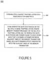
- FIG. 5is a process flow chart for forming a NAND string of an exemplary NAND flash memory device, according to one embodiment.
- multiple charge trapping layersare formed on a semiconductor substrate.
- respective gate electrodesare formed on the charge trapping layers, where the memory transistors are formed close to each other such that a channel is formed between an adjacent pair of the memory transistors based on a gate fringing effect associated with the adjacent pair of the memory transistors.
- a select line coupled to the NAND string of memory transistorsis formed, where the source select line comprises a source select transistor with a select gate at an intersection of the NAND string of memory transistors and the source select line.
Landscapes
- Semiconductor Memories (AREA)
- Non-Volatile Memory (AREA)
Abstract
Description
Claims (24)
Priority Applications (2)
| Application Number | Priority Date | Filing Date | Title |
|---|---|---|---|
| US16/380,209US11251189B2 (en) | 2009-02-09 | 2019-04-10 | Gate fringing effect based channel formation for semiconductor device |
| US17/670,975US11950412B2 (en) | 2009-02-09 | 2022-02-14 | Gate fringing effect based channel formation for semiconductor device |
Applications Claiming Priority (4)
| Application Number | Priority Date | Filing Date | Title |
|---|---|---|---|
| US12/368,023US8692310B2 (en) | 2009-02-09 | 2009-02-09 | Gate fringing effect based channel formation for semiconductor device |
| US14/179,316US9570458B2 (en) | 2009-02-09 | 2014-02-12 | Gate fringing effect based channel formation for semiconductor device |
| US15/403,422US10297606B2 (en) | 2009-02-09 | 2017-01-11 | Gate fringing effect based channel formation for semiconductor device |
| US16/380,209US11251189B2 (en) | 2009-02-09 | 2019-04-10 | Gate fringing effect based channel formation for semiconductor device |
Related Parent Applications (1)
| Application Number | Title | Priority Date | Filing Date |
|---|---|---|---|
| US15/403,422ContinuationUS10297606B2 (en) | 2009-02-09 | 2017-01-11 | Gate fringing effect based channel formation for semiconductor device |
Related Child Applications (1)
| Application Number | Title | Priority Date | Filing Date |
|---|---|---|---|
| US17/670,975ContinuationUS11950412B2 (en) | 2009-02-09 | 2022-02-14 | Gate fringing effect based channel formation for semiconductor device |
Publications (2)
| Publication Number | Publication Date |
|---|---|
| US20190319035A1 US20190319035A1 (en) | 2019-10-17 |
| US11251189B2true US11251189B2 (en) | 2022-02-15 |
Family
ID=42539704
Family Applications (5)
| Application Number | Title | Priority Date | Filing Date |
|---|---|---|---|
| US12/368,023ActiveUS8692310B2 (en) | 2009-02-09 | 2009-02-09 | Gate fringing effect based channel formation for semiconductor device |
| US14/179,316ActiveUS9570458B2 (en) | 2009-02-09 | 2014-02-12 | Gate fringing effect based channel formation for semiconductor device |
| US15/403,422ActiveUS10297606B2 (en) | 2009-02-09 | 2017-01-11 | Gate fringing effect based channel formation for semiconductor device |
| US16/380,209ActiveUS11251189B2 (en) | 2009-02-09 | 2019-04-10 | Gate fringing effect based channel formation for semiconductor device |
| US17/670,975ActiveUS11950412B2 (en) | 2009-02-09 | 2022-02-14 | Gate fringing effect based channel formation for semiconductor device |
Family Applications Before (3)
| Application Number | Title | Priority Date | Filing Date |
|---|---|---|---|
| US12/368,023ActiveUS8692310B2 (en) | 2009-02-09 | 2009-02-09 | Gate fringing effect based channel formation for semiconductor device |
| US14/179,316ActiveUS9570458B2 (en) | 2009-02-09 | 2014-02-12 | Gate fringing effect based channel formation for semiconductor device |
| US15/403,422ActiveUS10297606B2 (en) | 2009-02-09 | 2017-01-11 | Gate fringing effect based channel formation for semiconductor device |
Family Applications After (1)
| Application Number | Title | Priority Date | Filing Date |
|---|---|---|---|
| US17/670,975ActiveUS11950412B2 (en) | 2009-02-09 | 2022-02-14 | Gate fringing effect based channel formation for semiconductor device |
Country Status (1)
| Country | Link |
|---|---|
| US (5) | US8692310B2 (en) |
Families Citing this family (3)
| Publication number | Priority date | Publication date | Assignee | Title |
|---|---|---|---|---|
| US8692310B2 (en)* | 2009-02-09 | 2014-04-08 | Spansion Llc | Gate fringing effect based channel formation for semiconductor device |
| KR101515673B1 (en)* | 2011-06-13 | 2015-05-04 | 한양대학교 산학협력단 | 3-D Flash Memory of using Fringing Effect and Method of manufacturing the same |
| US9947664B1 (en) | 2016-10-14 | 2018-04-17 | International Business Machines Corporation | Semiconductor device and method of forming the semiconductor device |
Citations (268)
| Publication number | Priority date | Publication date | Assignee | Title |
|---|---|---|---|---|
| US5677556A (en)* | 1993-06-29 | 1997-10-14 | Kabushiki Kaisha Toshiba | Semiconductor device having inversion inducing gate |
| US6114182A (en) | 1998-03-18 | 2000-09-05 | Yamaha Corporation | Measurement of electron shading damage |
| US6117725A (en) | 1999-08-11 | 2000-09-12 | Taiwan Semiconductor Manufacturing Company | Method for making cost-effective embedded DRAM structures compatible with logic circuit processing |
| US6175522B1 (en) | 1999-09-30 | 2001-01-16 | Advanced Micro Devices, Inc. | Read operation scheme for a high-density, low voltage, and superior reliability nand flash memory device |
| US6242303B1 (en) | 1999-09-17 | 2001-06-05 | Worldwide Semiconductor Manufacturing Corp. | Nonvolatile memories with high capacitive-coupling ratio |
| US6249454B1 (en) | 1999-09-15 | 2001-06-19 | Taiwan Semiconductor Manufacturing Company | Split-gate flash cell for virtual ground architecture |
| US6255173B1 (en) | 1998-12-22 | 2001-07-03 | Hyundai Electronics Industries Co., Ltd. | Method of forming gate electrode with titanium polycide structure |
| US6281092B1 (en) | 1999-07-02 | 2001-08-28 | Lsi Logic Corporation | Method for manufacturing a metal-to-metal capacitor utilizing only one masking step |
| US6313497B1 (en) | 1999-02-15 | 2001-11-06 | Nec Corporation | Semiconductor device and method for manufacturing the same |
| US6326661B1 (en) | 1999-07-29 | 2001-12-04 | U.S. Philips Corporation | Semiconductor device |
| US6338993B1 (en) | 1999-08-18 | 2002-01-15 | Worldwide Semiconductor Manufacturing Corp. | Method to fabricate embedded DRAM with salicide logic cell structure |
| US6338998B1 (en) | 2000-11-15 | 2002-01-15 | Taiwan Semiconductor Manufacturing Company, Ltd | Embedded DRAM fabrication method providing enhanced embedded DRAM performance |
| US6376358B1 (en) | 2001-03-15 | 2002-04-23 | Micron Technology, Inc. | Method of forming plugs and local interconnect for embedded memory/system-on-chip (SOC) applications |
| US6385090B1 (en) | 2001-02-26 | 2002-05-07 | Fujitsu Limited | Semiconductor nonvolatile memory using floating gate |
| US6395590B1 (en) | 2000-08-15 | 2002-05-28 | Winbond Electronics Corporation | Capacitor plate formation in a mixed analog-nonvolatile memory device |
| US6426256B1 (en) | 1999-06-14 | 2002-07-30 | United Microelectronics Corp. | Method for fabricating an embedded DRAM with self-aligned borderless contacts |
| US6429479B1 (en) | 2000-03-09 | 2002-08-06 | Advanced Micro Devices, Inc. | Nand flash memory with specified gate oxide thickness |
| US6451653B2 (en) | 2000-05-15 | 2002-09-17 | Stmicroelectronics S.R.L. | Manufacturing process for the integration in a semiconductor chip of an integrated circuit including a high-density integrated circuit components portion and a high-performance logic integrated circuit components portion |
| US6462585B1 (en) | 2001-02-20 | 2002-10-08 | International Business Machines Corporation | High performance CPL double-gate latch |
| US6487117B1 (en) | 1999-02-01 | 2002-11-26 | Samsung Electronics Co., Ltd. | Method for programming NAND-type flash memory device using bulk bias |
| US6486050B1 (en) | 2002-02-21 | 2002-11-26 | Opto Tech Corporation | Method of manufacturing III-nitride semiconductor devices |
| US6501147B1 (en) | 1999-11-19 | 2002-12-31 | Stmicroelectronics S.R.L. | Process for manufacturing electronic devices comprising high voltage MOS transistors, and electronic device thus obtained |
| US6521934B2 (en) | 2001-03-28 | 2003-02-18 | Fujitsu Limited | Semiconductor device with a plurality of elements having different heights |
| US6521957B2 (en) | 1998-10-02 | 2003-02-18 | Stmicroelectronics S.R.L. | Method for forming a multilevel ROM memory in a dual gate CMOS process, and corresponding ROM memory cell |
| US6528414B1 (en) | 1998-08-18 | 2003-03-04 | Seiko Epson Corporation | Methods for forming wiring line structures in semiconductor devices |
| US6576517B1 (en) | 1998-12-31 | 2003-06-10 | Stmicroelectronics S.R.L. | Method for obtaining a multi-level ROM in an EEPROM process flow |
| US6579757B2 (en) | 2000-11-22 | 2003-06-17 | Hynix Semiconductor Inc. | Method for fabricating semiconductor device which prevents gates of a peripheral region from being oxidized |
| US6650566B2 (en) | 2000-12-12 | 2003-11-18 | Samsung Electronics Co., Ltd. | Nonvolatile semiconductor memory with a programming operation and the method thereof |
| US6661707B2 (en) | 2001-02-16 | 2003-12-09 | Samsung Electronics Co., Ltd. | Method of programming NAND-type flash memory |
| US6699754B2 (en) | 2002-04-24 | 2004-03-02 | Nanya Technology Corporation | Flash memory cell and method for fabricating the same |
| US6720613B1 (en) | 2003-01-15 | 2004-04-13 | Macronix International Co., Ltd. | Method of fabricating multi-bit flash memory |
| US6727544B2 (en)* | 2001-03-30 | 2004-04-27 | Fujio Masuoka | Semiconductor memory including cell(s) with both charge storage layer(s) and control gate laterally surrounding island-like semiconductor layer |
| US6734106B2 (en) | 2001-10-03 | 2004-05-11 | Promos Technologies, Inc. | Method of buried strap out-diffusion formation by gas phase doping |
| US6774428B1 (en) | 2003-04-03 | 2004-08-10 | Powerchip Semiconductor Corp. | Flash memory structure and operating method thereof |
| US6783997B2 (en) | 2001-12-19 | 2004-08-31 | Texas Instruments Incorporated | Gate structure and method |
| US6797570B2 (en) | 2000-01-17 | 2004-09-28 | Samsung Electronics Co., Ltd. | NAND-type flash memory devices and methods of fabricating the same |
| US6800515B2 (en) | 2001-11-28 | 2004-10-05 | Stmicroelectronics S.A. | DRAM and MOS transistor manufacturing |
| EP1181694B1 (en) | 1999-06-01 | 2004-12-29 | Infineon Technologies AG | Plateline sensing |
| US6888773B2 (en) | 2002-12-05 | 2005-05-03 | Sharp Kabushiki Kaisha | Semiconductor memory device and erase method for memory array |
| US6898120B2 (en) | 2002-12-10 | 2005-05-24 | Seiko Epson Corporation | Nonvolatile semiconductor memory device |
| US6936885B2 (en) | 2000-01-17 | 2005-08-30 | Samsung Electronics Co., Ltd. | NAND-type flash memory devices and methods of fabricating the same |
| US6977842B2 (en) | 2003-09-16 | 2005-12-20 | Micron Technology, Inc. | Boosted substrate/tub programming for flash memories |
| US6995410B2 (en) | 2002-08-20 | 2006-02-07 | Kabushiki Kaisha Toshiba | NAND flash memory with unequal spacing between signal lines |
| US7002845B2 (en) | 1998-07-02 | 2006-02-21 | Kabushiki Kaisha Toshiba | Semiconductor memory device capable of realizing a chip with high operation reliability and high yield |
| US7009244B2 (en) | 2003-07-02 | 2006-03-07 | Integrated Memory Technologies, Inc. | Scalable flash EEPROM memory cell with notched floating gate and graded source region |
| US7009888B2 (en) | 2003-07-15 | 2006-03-07 | Sharp Kabushiki Kaisha | Low voltage, island-layer-based nonvolatile semiconductor storage device with floating biased memory cell channel |
| US7015540B2 (en) | 2002-10-30 | 2006-03-21 | Renesas Technology Corp. | Semiconductor memory device |
| US7031194B2 (en) | 2003-08-29 | 2006-04-18 | Seiko Epson Corporation | Nonvolatile semiconductor memory and method for controlling the same |
| US7061275B2 (en) | 2003-08-15 | 2006-06-13 | Klp International, Ltd. | Field programmable gate array |
| US7064031B2 (en) | 2004-03-08 | 2006-06-20 | United Microelectronics Corp. | Method for forming a semiconductor device |
| US20060138563A1 (en) | 2004-12-28 | 2006-06-29 | Hynix Semiconductor Inc. | Nand flash memory device |
| US7091522B2 (en) | 2003-07-29 | 2006-08-15 | Industrial Research Technology Institute | Strained silicon carbon alloy MOSFET structure and fabrication method thereof |
| US7105888B2 (en) | 2002-03-27 | 2006-09-12 | Nec Electronics Corporation | Nonvolatile semiconductor memory device and method of manufacturing same |
| US7118972B2 (en) | 2003-04-28 | 2006-10-10 | Renesas Technology Corp. | Method of manufacture of a semiconductor device |
| US7118968B2 (en) | 2004-08-17 | 2006-10-10 | Macronix International Co., Ltd. | Method for manufacturing interpoly dielectric |
| US7148538B2 (en) | 2003-12-17 | 2006-12-12 | Micron Technology, Inc. | Vertical NAND flash memory array |
| US7157771B2 (en) | 2004-01-30 | 2007-01-02 | Micron Technology, Inc. | Vertical device 4F2 EEPROM memory |
| EP1513160B1 (en) | 2003-09-04 | 2007-01-03 | Macronix International Co., Ltd. | A non-volatile flash memory |
| US7161833B2 (en) | 2004-02-06 | 2007-01-09 | Sandisk Corporation | Self-boosting system for flash memory cells |
| US7187029B2 (en) | 2001-08-31 | 2007-03-06 | Sharp Kabushiki Kaisha | Nonvolatile semiconductor memory device with floating gate and two control gates |
| US7190024B2 (en) | 2003-11-14 | 2007-03-13 | Samsung Electronics, Co., Ltd. | Method of manufacturing a thin dielectric layer using a heat treatment and a semiconductor device formed using the method |
| US7196930B2 (en) | 2005-04-27 | 2007-03-27 | Micron Technology, Inc. | Flash memory programming to reduce program disturb |
| US7208419B2 (en) | 2003-02-19 | 2007-04-24 | Hynix Semiconductor Inc. | Method for fabricating semiconductor device |
| US7217621B2 (en) | 2004-03-17 | 2007-05-15 | Silicon Storage Technology, Inc | Self-aligned split-gate NAND flash memory and fabrication process |
| US7223659B2 (en) | 2002-05-23 | 2007-05-29 | Samsung Electronics Co., Ltd. | Memory device and fabrication method thereof |
| US7232722B2 (en) | 2002-06-24 | 2007-06-19 | Interuniversitair Microelektronica Centrum Vzw | Method of making a multibit non-volatile memory |
| US7238571B1 (en)* | 2005-02-24 | 2007-07-03 | Advanced Micro Devices, Inc. | Non-volatile memory device with increased reliability |
| US7247907B2 (en) | 2005-05-20 | 2007-07-24 | Silicon Storage Technology, Inc. | Bidirectional split gate NAND flash memory structure and array, method of programming, erasing and reading thereof, and method of manufacturing |
| US20070205445A1 (en) | 2005-12-20 | 2007-09-06 | Park Ki-Tae | Semiconductor device having a field effect source/drain region |
| US7285816B2 (en) | 2003-08-29 | 2007-10-23 | Stmicroelectronics S.R.L. | Content addressable matrix memory cell |
| US7303964B2 (en) | 2005-04-25 | 2007-12-04 | Spansion Llc | Self-aligned STI SONOS |
| US7319611B2 (en) | 2006-01-25 | 2008-01-15 | Macronix International Co., Ltd. | Bitline transistor architecture for flash memory |
| US7320931B2 (en) | 2004-07-30 | 2008-01-22 | Freescale Semiconductor Inc. | Interfacial layer for use with high k dielectric materials |
| US7326988B2 (en) | 2002-07-02 | 2008-02-05 | Matsushita Electric Industrial Co., Ltd. | Semiconductor device and method for fabricating the same |
| US7339239B2 (en) | 2003-12-17 | 2008-03-04 | Micron Technology, Inc. | Vertical NROM NAND flash memory array |
| EP1308962B1 (en) | 2001-11-02 | 2008-03-05 | eMemory Technology Inc. | Single poly embedded EPROM |
| US7348245B2 (en) | 2003-04-28 | 2008-03-25 | Renesas Technology Corp. | Semiconductor device and a method of manufacturing the same |
| US20080117683A1 (en)* | 2006-11-16 | 2008-05-22 | Gerrit Jan Hemink | Controlled boosting in non-volatile memory soft programming |
| US7378336B2 (en) | 2003-10-07 | 2008-05-27 | International Business Machines Corporation | Split poly-SiGe/poly-Si alloy gate stack |
| EP1777708B1 (en) | 2005-10-18 | 2008-05-28 | Kilopass Technology, Inc. | 3.5 Transistor non-volatile memory cell using gate breakdown phenomena |
| US7385249B2 (en) | 2003-02-20 | 2008-06-10 | Taiwan Semiconductor Manufacturing Company | Transistor structure and integrated circuit |
| US20080135912A1 (en)* | 2006-12-07 | 2008-06-12 | Samsung Electronics Co., Ltd. | Memory device and method of fabricating the same |
| KR100843713B1 (en) | 2006-10-23 | 2008-07-04 | 삼성전자주식회사 | Method of fabricating a semiconductor device having fine contact hole |
| US7397080B2 (en) | 2005-06-27 | 2008-07-08 | Powerchip Semiconductor Corp. | Non-volatile memory |
| US7402492B2 (en) | 2005-03-21 | 2008-07-22 | Samsung Electronics Co., Ltd. | Method of manufacturing a memory device having improved erasing characteristics |
| US7411241B2 (en) | 2005-03-28 | 2008-08-12 | Samsung Electronics Co., Ltd. | Vertical type nanotube semiconductor device |
| US7410872B2 (en) | 2003-10-22 | 2008-08-12 | Stmicroelectronics S.R.L. | Sealing method for electronic devices formed on a common semiconductor substrate and corresponding circuit structure |
| US7416940B1 (en)* | 2006-05-03 | 2008-08-26 | Spansion Llc | Methods for fabricating flash memory devices |
| US7419870B2 (en) | 2004-08-26 | 2008-09-02 | Hynix Semiconductor Inc. | Method of manufacturing a flash memory device |
| US7432183B2 (en) | 2004-12-20 | 2008-10-07 | Samsung Electronics Co., Ltd. | Methods of manufacturing a thin film including zirconium titanium oxide and methods of manufacturing a gate structure, a capacitor and a flash memory device including the same |
| US7432206B2 (en) | 2006-01-24 | 2008-10-07 | Macronix International Co., Ltd. | Self-aligned manufacturing method, and manufacturing method for thin film fuse phase change ram |
| US7435637B2 (en) | 2000-03-01 | 2008-10-14 | Intel Corporation | Quantum wire gate device and method of making same |
| US20080259688A1 (en)* | 2007-04-19 | 2008-10-23 | Samsung Electronics Co., Ltd. | Non-volatile memory devices and methods of operating the same |
| US20080273389A1 (en)* | 2007-03-21 | 2008-11-06 | Micron Technology, Inc. | Flash memory cells, NAND cell units, methods of forming NAND cell units, and methods of programming NAND cell unit strings |
| US7449744B1 (en) | 2004-08-03 | 2008-11-11 | Nanostar Corporation | Non-volatile electrically alterable memory cell and use thereof in multi-function memory array |
| US7457156B2 (en) | 2004-09-02 | 2008-11-25 | Micron Technology, Inc. | NAND flash depletion cell structure |
| EP1829044B1 (en) | 2004-12-23 | 2008-11-26 | SanDisk Corporation | Substrate electron injection techniques for programming non-volatile charge storage memory cells |
| US7459390B2 (en) | 2006-03-20 | 2008-12-02 | Texas Instruments Incorporated | Method for forming ultra thin low leakage multi gate devices |
| US7466590B2 (en) | 2004-02-06 | 2008-12-16 | Sandisk Corporation | Self-boosting method for flash memory cells |
| EP1636803B1 (en) | 2003-06-20 | 2008-12-24 | SanDisk Corporation | Source controlled operation of non-volatile memories |
| US20080318381A1 (en)* | 2007-06-20 | 2008-12-25 | George Matamis | Methods of forming high density semiconductor devices using recursive spacer technique |
| US7473963B2 (en) | 2003-08-05 | 2009-01-06 | Samsung Electronics Co., Ltd. | Metal oxide semiconductor (MOS) transistors having three dimensional channels |
| US7485530B2 (en) | 2004-07-06 | 2009-02-03 | Macronix International Co., Ltd. | Method for manufacturing a multiple-gate charge trapping non-volatile memory |
| US7489010B2 (en) | 2005-05-27 | 2009-02-10 | Kabushiki Kaisha Toshiba | Semiconductor memory device |
| US7491622B2 (en) | 2006-04-24 | 2009-02-17 | Freescale Semiconductor, Inc. | Process of forming an electronic device including a layer formed using an inductively coupled plasma |
| US7495267B2 (en) | 2003-09-08 | 2009-02-24 | Taiwan Semiconductor Manufacturing Company, Ltd. | Semiconductor structure having a strained region and a method of fabricating same |
| US7495282B2 (en) | 2007-01-12 | 2009-02-24 | Sandisk Corporation | NAND memory with virtual channel |
| US7510929B2 (en) | 2006-10-18 | 2009-03-31 | Macronix International Co., Ltd. | Method for making memory cell device |
| US7521348B2 (en) | 2006-10-23 | 2009-04-21 | Samsung Electronics Co., Ltd. | Method of fabricating semiconductor device having fine contact holes |
| US7521364B2 (en) | 2005-12-02 | 2009-04-21 | Macronix Internation Co., Ltd. | Surface topology improvement method for plug surface areas |
| US20090103371A1 (en)* | 2007-10-22 | 2009-04-23 | Micron Technology, Inc. | Memory cell operation |
| US7544566B2 (en) | 2005-01-14 | 2009-06-09 | Nanostar Corporation | Method for manufacturing a non-volatile electrically alterable memory cell that stores multiple data |
| US7544984B2 (en) | 2003-07-21 | 2009-06-09 | Micron Technology, Inc. | Gettering using voids formed by surface transformation |
| US7547949B2 (en) | 2004-05-26 | 2009-06-16 | Micron Technology, Inc. | Semiconductor structures and memory device constructions |
| US7547941B2 (en) | 2006-05-04 | 2009-06-16 | Elite Semiconductor Memory Technology, Inc. | NAND non-volatile two-bit memory and fabrication method |
| US7550353B2 (en) | 2006-11-01 | 2009-06-23 | Samsung Electronics Co., Ltd. | Method of forming semiconductor device |
| US7582529B2 (en) | 2007-04-02 | 2009-09-01 | Sandisk Corporation | Methods of fabricating non-volatile memory with integrated peripheral circuitry and pre-isolation memory cell formation |
| US7601591B2 (en) | 2005-05-19 | 2009-10-13 | Micron Technology, Inc. | Method of manufacturing sidewall spacers on a memory device, and device comprising same |
| US7608882B2 (en) | 2003-08-11 | 2009-10-27 | Macronix International Co., Ltd. | Split-gate non-volatile memory |
| US7615820B2 (en) | 2004-11-23 | 2009-11-10 | Sandisk Corporation | Self-aligned trenches with grown dielectric for high coupling ratio in semiconductor devices |
| US7623389B2 (en) | 2006-12-21 | 2009-11-24 | Sandisk Corporation | System for low voltage programming of non-volatile memory cells |
| US7626226B2 (en) | 2001-04-27 | 2009-12-01 | Interuniversitair Microelektronica Centrum (Imec) | Method for improving erase saturation in non-volatile memory devices and devices obtained thereof |
| US7633803B2 (en) | 2007-05-10 | 2009-12-15 | Samsung Electronics Co., Ltd. | Methods of operating memory devices including negative incremental step pulse programming and related devices |
| US7638402B2 (en) | 2006-12-28 | 2009-12-29 | Texas Instruments Incorporated | Sidewall spacer pullback scheme |
| DE102009023789A1 (en) | 2008-06-11 | 2009-12-31 | Samsung Electronics Co., Ltd., Suwon | Vertical column memory devices and methods of making and operating the same |
| US7642160B2 (en) | 2006-12-21 | 2010-01-05 | Sandisk Corporation | Method of forming a flash NAND memory cell array with charge storage elements positioned in trenches |
| US7646641B2 (en) | 2004-06-15 | 2010-01-12 | Silicon Storage Technology, Inc. | NAND flash memory with nitride charge storage gates and fabrication process |
| US7652340B2 (en) | 2004-12-03 | 2010-01-26 | Samsung Electronics Co., Ltd. | Fin field effect transistor and method of manufacturing the same |
| US7663177B2 (en) | 2005-08-03 | 2010-02-16 | Industrial Technology Research Institute | Non-volatile memory device and fabricating method thereof |
| US7666800B2 (en) | 2008-02-13 | 2010-02-23 | Infineon Technologies Ag | Feature patterning methods |
| EP1538633B1 (en) | 2003-12-01 | 2010-03-03 | Samsung Electronics Co., Ltd. | Flash memory device and method for programming the same |
| US7687307B2 (en) | 2005-11-21 | 2010-03-30 | Macronix International Co., Ltd. | Vacuum jacketed electrode for phase change memory element |
| US7691689B2 (en) | 2005-11-04 | 2010-04-06 | Samsung Electronics Co., Ltd. | Methods of fabricating semiconductor devices having multiple channel transistors and semiconductor devices fabricated thereby |
| US7696552B2 (en) | 2004-09-16 | 2010-04-13 | Samsung Electronics Co., Ltd. | Semiconductor devices including high-k dielectric materials |
| US7701771B2 (en) | 2006-08-04 | 2010-04-20 | Samsung Electronics Co., Ltd. | Memory device including 3-dimensionally arranged memory cell transistors and methods of operating the same |
| US7709884B2 (en) | 2002-01-15 | 2010-05-04 | Infineon Technologies Ag | Non-volatile two transistor semiconductor memory cell and method for producing the same |
| US7709836B2 (en) | 2002-03-14 | 2010-05-04 | Infineon Technologies Ag | Detector arrangement, method for the detection of electrical charge carriers and use of an ONO field effect transistor for detection of an electrical charge |
| US7714372B2 (en) | 2007-02-22 | 2010-05-11 | Samsung Electronics Co., Ltd. | Dynamic random access memory devices and methods of forming the same |
| US7713854B2 (en) | 2006-10-20 | 2010-05-11 | Taiwan Semiconductor Manufacturing Co., Ltd. | Gate dielectric layers and methods of fabricating gate dielectric layers |
| US7736959B2 (en) | 2003-07-22 | 2010-06-15 | Innovative Silicon Isi Sa | Integrated circuit device, and method of fabricating same |
| US7745285B2 (en) | 2007-03-30 | 2010-06-29 | Sandisk Corporation | Methods of forming and operating NAND memory with side-tunneling |
| US7750415B2 (en) | 2006-01-09 | 2010-07-06 | International Business Machines Corporation | Structure and method for making high density MOSFET circuits with different height contact lines |
| US7749854B2 (en) | 2006-12-06 | 2010-07-06 | Macronix International Co., Ltd. | Method for making a self-converged memory material element for memory cell |
| US7759719B2 (en) | 2004-07-01 | 2010-07-20 | Chih-Hsin Wang | Electrically alterable memory cell |
| US7767588B2 (en) | 2006-02-28 | 2010-08-03 | Freescale Semiconductor, Inc. | Method for forming a deposited oxide layer |
| US7772060B2 (en) | 2006-06-21 | 2010-08-10 | Texas Instruments Deutschland Gmbh | Integrated SiGe NMOS and PMOS transistors |
| US7785993B2 (en) | 2004-11-02 | 2010-08-31 | Nxp B.V. | Method of growing a strained layer |
| US7795119B2 (en) | 2007-07-17 | 2010-09-14 | Taiwan Semiconductor Manufacturing Company, Ltd. | Flash anneal for a PAI, NiSi process |
| US7807529B2 (en) | 2007-12-19 | 2010-10-05 | Sandisk Corporation | Lithographically space-defined charge storage regions in non-volatile memory |
| US7816270B2 (en) | 2008-05-19 | 2010-10-19 | Samsung Electronics Co., Ltd. | Method of forming minute patterns in semiconductor device using double patterning |
| US7816723B2 (en) | 2004-06-07 | 2010-10-19 | Silicon Storage Technology, Inc. | Semiconductor memory array of floating gate memory cells with program/erase and select gates |
| US7824994B2 (en) | 2006-07-14 | 2010-11-02 | Micron Technology, Inc. | Method of forming memory devices by performing halogen ion implantation and diffusion processes |
| US7825462B2 (en) | 2004-09-01 | 2010-11-02 | Micron Technology, Inc. | Transistors |
| US7825398B2 (en) | 2008-04-07 | 2010-11-02 | Macronix International Co., Ltd. | Memory cell having improved mechanical stability |
| EP1552529B1 (en) | 2002-05-29 | 2010-11-03 | Micron Technology, Inc. | Method and apparatus for erasing flash memory |
| US7834388B2 (en) | 2004-03-16 | 2010-11-16 | Nanostar Corporation | Memory array of non-volatile electrically alterable memory cells for storing multiple data |
| US7842536B2 (en) | 2005-11-21 | 2010-11-30 | Macronix International Co., Ltd. | Vacuum jacket for phase change memory element |
| US7843015B2 (en) | 2003-11-03 | 2010-11-30 | Globalfoundries Inc. | Multi-silicide system in integrated circuit technology |
| EP1573745B1 (en) | 2002-12-12 | 2010-12-01 | Actel Corporation | Programmable interconnect cell for configuring a field programmable gate array |
| US7847341B2 (en) | 2006-12-20 | 2010-12-07 | Nanosys, Inc. | Electron blocking layers for electronic devices |
| US7846843B2 (en) | 2007-06-29 | 2010-12-07 | Hynix Semiconductor Inc. | Method for manufacturing a semiconductor device using a spacer as an etch mask for forming a fine pattern |
| US7851847B2 (en) | 2006-12-27 | 2010-12-14 | Hynix Semiconductor Inc. | Flash memory device and method of erasing the same |
| US7859050B2 (en) | 2007-01-22 | 2010-12-28 | Micron Technology, Inc. | Memory having a vertical access device |
| US7858472B2 (en) | 2001-08-08 | 2010-12-28 | Sandisk Corporation | Scalable self-aligned dual floating gate memory cell array and methods of forming the array |
| US7863655B2 (en) | 2006-10-24 | 2011-01-04 | Macronix International Co., Ltd. | Phase change memory cells with dual access devices |
| US7867815B2 (en) | 2005-11-16 | 2011-01-11 | Macronix International Co., Ltd. | Spacer electrode small pin phase change RAM and manufacturing method |
| US7884342B2 (en) | 2007-07-31 | 2011-02-08 | Macronix International Co., Ltd. | Phase change memory bridge cell |
| US7888203B2 (en) | 2005-04-04 | 2011-02-15 | Samsung Electronics Co., Ltd. | Methods of making nonvolatile memory devices |
| US7888210B2 (en) | 2007-12-19 | 2011-02-15 | Sandisk Corporation | Non-volatile memory fabrication and isolation for composite charge storage structures |
| US7893418B2 (en) | 2007-12-07 | 2011-02-22 | Macronix International Co., Ltd. | Phase change memory cell having interface structures with essentially equal thermal impedances and manufacturing methods |
| US7897954B2 (en) | 2008-10-10 | 2011-03-01 | Macronix International Co., Ltd. | Dielectric-sandwiched pillar memory device |
| US7898019B2 (en) | 2007-01-12 | 2011-03-01 | Micron Technology, Inc. | Semiconductor constructions having multiple patterned masking layers over NAND gate stacks |
| US7902589B2 (en) | 2006-02-17 | 2011-03-08 | Macronix International Co., Ltd. | Dual gate multi-bit semiconductor memory array |
| US7907448B2 (en) | 2008-10-07 | 2011-03-15 | Spansion Llc | Scaled down select gates of NAND flash memory cell strings and method of forming same |
| US7910906B2 (en) | 2006-10-04 | 2011-03-22 | Macronix International Co., Ltd. | Memory cell device with circumferentially-extending memory element |
| US7910434B2 (en) | 2006-09-21 | 2011-03-22 | Sandisk Corporation | Method of reducing coupling between floating gates in nonvolatile memory |
| US7910974B2 (en) | 2004-10-29 | 2011-03-22 | Spansion Llc | Semiconductor device and method for fabricating thereof |
| US7915664B2 (en) | 2008-04-17 | 2011-03-29 | Sandisk Corporation | Non-volatile memory with sidewall channels and raised source/drain regions |
| US7919413B2 (en) | 2007-08-06 | 2011-04-05 | Industrial Technology Research Institute | Methods for forming patterns |
| US7919799B2 (en) | 2003-02-21 | 2011-04-05 | Renesas Electronics Corporation | Semiconductor device and semiconductor device manufacturing method |
| US7919829B2 (en) | 2004-08-24 | 2011-04-05 | Micron Technology, Inc. | Liner for shallow trench isolation |
| US7936005B2 (en) | 2008-05-29 | 2011-05-03 | Kabushiki Kaisha Toshiba | Semiconductor memory device including laminated gate having electric charge accumulating layer and control gate and method of manufacturing the same |
| US7939451B2 (en) | 2007-06-07 | 2011-05-10 | Macronix International Co., Ltd. | Method for fabricating a pattern |
| US7944023B2 (en) | 2004-06-03 | 2011-05-17 | Taiwan Semiconductor Manufacturing Company, Ltd. | Strained Si formed by anneal |
| US7944749B2 (en) | 2006-12-21 | 2011-05-17 | Sandisk Corporation | Method of low voltage programming of non-volatile memory cells |
| US7943452B2 (en) | 2006-12-12 | 2011-05-17 | International Business Machines Corporation | Gate conductor structure |
| US7960803B2 (en) | 2005-02-23 | 2011-06-14 | Micron Technology, Inc. | Electronic device having a hafnium nitride and hafnium oxide film |
| US7977729B2 (en) | 2007-07-17 | 2011-07-12 | Kabushiki Kaisha Toshiba | Aging device |
| US7989914B2 (en) | 2004-12-27 | 2011-08-02 | Stmicroelectronics Crolles 2 Sas | Anti-fuse cell and its manufacturing process |
| US8008114B2 (en) | 2005-11-15 | 2011-08-30 | Macronix International Co., Ltd. | Phase change memory device and manufacturing method |
| US8026535B2 (en) | 2007-03-22 | 2011-09-27 | Hitachi, Ltd. | Thin film transistor and organic electroluminescence display using the same |
| US8030634B2 (en) | 2008-03-31 | 2011-10-04 | Macronix International Co., Ltd. | Memory array with diode driver and method for fabricating the same |
| US8030160B2 (en) | 2007-03-29 | 2011-10-04 | Sandisk Technologies Inc. | Methods of forming NAND flash memory with fixed charge |
| US8039348B2 (en) | 2006-03-02 | 2011-10-18 | Micron Technology, Inc. | Vertical gated access transistor |
| US8044452B2 (en) | 2003-03-24 | 2011-10-25 | Rohm Co., Ltd. | Semiconductor device and method for manufacturing the same |
| US8063433B2 (en) | 2007-04-27 | 2011-11-22 | Renesas Electronics Corporation | Nonvolatile semiconductor memory device |
| US8072023B1 (en) | 2007-11-12 | 2011-12-06 | Marvell International Ltd. | Isolation for non-volatile memory cell array |
| US8084353B2 (en) | 2004-02-03 | 2011-12-27 | Macronix International Co., Ltd. | Methods for pitch reduction formation |
| US8088664B2 (en) | 2006-10-17 | 2012-01-03 | Texas Instruments Deutschland Gmbh | Method of manufacturing integrated deep and shallow trench isolation structures |
| US8097487B2 (en) | 2005-11-21 | 2012-01-17 | Macronix International Co., Ltd. | Method for making a phase change memory device with vacuum cell thermal isolation |
| US8101992B2 (en) | 2005-05-13 | 2012-01-24 | Micron Technology, Inc. | Memory array with surrounding gate access transistors and capacitors with global and staggered local bit lines |
| US8105909B2 (en) | 2008-04-07 | 2012-01-31 | Hynix Semiconductor Inc. | Method of fabricating non-volatile memory device |
| US8110507B2 (en) | 2008-06-20 | 2012-02-07 | Hynix Semiconductor Inc. | Method for patterning an active region in a semiconductor device using a space patterning process |
| US8119481B2 (en) | 2007-08-27 | 2012-02-21 | Macronix International Co., Ltd. | High-κ capped blocking dielectric bandgap engineered SONOS and MONOS |
| US8138526B2 (en) | 2007-07-17 | 2012-03-20 | Micron Technology, Inc. | Semiconductor structures including dual fins |
| EP1884956B1 (en) | 2006-07-27 | 2012-03-21 | Samsung Electronics Co., Ltd. | Non-volatile memory device having pass transistors and method of operating the same |
| US8174062B2 (en) | 2005-03-23 | 2012-05-08 | Renesas Electronics Corporation | Semiconductor memory device and manufacturing method thereof |
| US8183613B2 (en) | 2009-01-09 | 2012-05-22 | Samsung Electronics Co., Ltd. | Bipolar transistor for a memory array |
| US8188536B2 (en) | 2006-06-26 | 2012-05-29 | Macronix International Co., Ltd. | Memory device and manufacturing method and operating method thereof |
| US8188533B2 (en) | 2002-06-21 | 2012-05-29 | Micron Technology, Inc. | Write once read only memory employing charge trapping in insulators |
| JP4969748B2 (en) | 1999-08-27 | 2012-07-04 | マクロニックス・アメリカ・インコーポレーテッド | Nonvolatile semiconductor memory device and method of manufacturing nonvolatile memory cell |
| US8222071B2 (en) | 2007-10-22 | 2012-07-17 | Macronix International Co., Ltd. | Method for making self aligning pillar memory cell device |
| US8223549B2 (en) | 2006-07-28 | 2012-07-17 | Micron Technology, Inc. | NAND flash memory programming |
| US8227355B2 (en) | 2006-01-19 | 2012-07-24 | Fujitsu Semiconductor Limited | Method and apparatus of fabricating semiconductor device |
| DE102007031278B4 (en) | 2006-07-11 | 2012-08-02 | Samsung Electronics Co., Ltd. | Nonvolatile memory devices with dummy word lines and related structures and methods |
| US8243518B2 (en) | 2008-05-19 | 2012-08-14 | Samsung Electronics Co., Ltd. | NAND flash memory device and method of making same |
| US8252646B2 (en) | 2005-09-01 | 2012-08-28 | Micron Technology, Inc. | Peripheral gate stacks and recessed array gates |
| EP2264756B1 (en) | 2008-03-31 | 2012-08-29 | Fujitsu Semiconductor Limited | Semiconductor device |
| US8278156B2 (en) | 2008-01-16 | 2012-10-02 | Cadence Design Systems, Inc. | Spacer double patterning for lithography operations |
| US8283253B2 (en) | 2008-02-15 | 2012-10-09 | Tokyo Electron Limited | Pattern forming method, semiconductor device manufacturing method and semiconductor device manufacturing apparatus |
| US8293613B2 (en) | 2007-03-12 | 2012-10-23 | Samsung Electronics Co., Ltd. | Gettering structures and methods and their application |
| US8318569B2 (en) | 2008-12-01 | 2012-11-27 | Samsung Electronics Co., Ltd. | Forming memory cells comprising impurity doping regions along edges of less than 1F spacing |
| US8383495B2 (en) | 2006-02-02 | 2013-02-26 | Siltronic Ag | Semiconductor layer structure and method for fabricating a semiconductor layer structure |
| EP1579479B1 (en) | 2002-04-26 | 2013-03-13 | Kilopass Technology, Inc. | High density semiconductor memory cell and memory array using a single transistor |
| TWI392063B (en) | 2005-08-31 | 2013-04-01 | Samsung Electronics Co Ltd | Method for manufacturing charge trapping dielectric and method for fabricating non-volatile semiconductor device of cerium-oxide-nitride-oxide-germanium (SONOS) type |
| US8426272B2 (en) | 2008-06-05 | 2013-04-23 | Samsung Electronics Co., Ltd. | Non-volatile memory devices including shared bit lines and methods of fabricating the same |
| US8456918B2 (en) | 2008-04-14 | 2013-06-04 | Samsung Electronics Co., Ltd. | NAND flash memory device and method of operating same to reduce a difference between channel potentials therein |
| US8471307B2 (en) | 2008-06-13 | 2013-06-25 | Texas Instruments Incorporated | In-situ carbon doped e-SiGeCB stack for MOS transistor |
| US8471295B2 (en) | 2006-12-04 | 2013-06-25 | Snu R&Db Foundation | High density flash memory device, cell string and fabricating method thereof |
| US8488381B2 (en) | 2009-02-02 | 2013-07-16 | Samsung Electronics Co., Ltd. | Non-volatile memory device having vertical structure and method of operating the same |
| TWI405244B (en) | 2008-12-04 | 2013-08-11 | Micron Technology Inc | Methods of fabricating substrates |
| TWI405243B (en) | 2008-10-09 | 2013-08-11 | Micron Technology Inc | Methods of forming patterns utilizing lithography and spacers |
| TWI406360B (en) | 2008-12-04 | 2013-08-21 | Micron Technology Inc | Methods of fabricating substrates |
| US8519466B2 (en) | 2006-08-31 | 2013-08-27 | Micron Technology, Inc. | Tantalum silicon oxynitride high-K dielectrics and metal gates |
| TWI408752B (en) | 2008-02-19 | 2013-09-11 | Micron Technology Inc | Fin-type transistor element with gate short circuit and manufacturing method thereof |
| US8546215B2 (en) | 2005-08-31 | 2013-10-01 | Micron Technology, Inc. | Methods of fabricating a memory device |
| US8546152B2 (en) | 2007-12-19 | 2013-10-01 | Sandisk Technologies Inc. | Enhanced endpoint detection in non-volatile memory fabrication processes |
| US8546251B1 (en) | 2008-12-31 | 2013-10-01 | Synopsys, Inc. | Compact read only memory cell |
| EP1514309B1 (en) | 2002-06-19 | 2013-11-27 | SanDisk Technologies Inc. | Deep wordline trench to shield cross coupling between adjacent cells of nand memory |
| US8609487B2 (en) | 2006-04-14 | 2013-12-17 | Kabushiki Kaisha Toshiba | Method of manufacturing semiconductor device |
| US8685859B2 (en) | 2008-09-11 | 2014-04-01 | Micron Technology, Inc. | Self-aligned semiconductor trench structures |
| US8692310B2 (en)* | 2009-02-09 | 2014-04-08 | Spansion Llc | Gate fringing effect based channel formation for semiconductor device |
| US8735963B2 (en) | 2008-07-07 | 2014-05-27 | Taiwan Semiconductor Manufacturing Company, Ltd. | Flash memory cells having leakage-inhibition layers |
| US8735297B2 (en) | 2004-05-06 | 2014-05-27 | Sidense Corporation | Reverse optical proximity correction method |
| US8759170B2 (en) | 2006-08-31 | 2014-06-24 | Micron Technology, Inc. | Hafnium tantalum oxynitride dielectric |
| US8766410B2 (en) | 2007-10-30 | 2014-07-01 | International Business Machines Corporation | Embedded DRAM integrated circuits with extremely thin silicon-on-insulator pass transistors |
| US8772840B2 (en) | 2006-03-02 | 2014-07-08 | Micron Technology, Inc. | Memory device comprising an array portion and a logic portion |
| US8796770B2 (en) | 2007-01-26 | 2014-08-05 | Micron Technology, Inc. | Semiconductor device with electrically floating body |
| US8878282B2 (en) | 2008-11-06 | 2014-11-04 | Kabushiki Kaisha Toshiba | Nonvolatile semiconductor storage device and method of manufacture thereof |
| US8877589B2 (en) | 2005-08-30 | 2014-11-04 | Micron Technology, Inc. | Methods of forming field effect transistors on substrates |
| US8916912B2 (en) | 2005-07-08 | 2014-12-23 | Micron Technology, Inc. | Semiconductor device comprising a transistor gate having multiple vertically oriented sidewalls |
| US8937340B2 (en) | 2005-01-03 | 2015-01-20 | Macronix International Co., Ltd. | Silicon on insulator and thin film transistor bandgap engineered split gate memory |
| US8963226B2 (en) | 2004-08-09 | 2015-02-24 | Renesas Electronics Corporation | Semiconductor device with gate electrodes |
| US9070791B2 (en) | 2006-11-15 | 2015-06-30 | International Business Machines Corporation | Tunable capacitor |
| KR101535227B1 (en) | 2008-12-31 | 2015-07-08 | 삼성전자주식회사 | Method for forming fine pattern using block copolymer |
| US9082829B2 (en) | 2005-09-01 | 2015-07-14 | Micron Technology, Inc. | Methods for forming arrays of small, closely spaced features |
| US9214525B2 (en) | 2006-12-20 | 2015-12-15 | Sandisk Corporation | Gate stack having electron blocking layers on charge storage layers for electronic devices |
| EP2290642B1 (en) | 2001-09-21 | 2015-12-23 | Semiconductor Energy Laboratory Co., Ltd. | Semiconductor device for a TFTdisplay matrix |
| USRE45832E1 (en) | 2008-11-14 | 2016-01-05 | Kabushiki Kaisha Toshiba | Non-volatile semiconductor storage device |
| DE102009052705B4 (en) | 2009-01-07 | 2016-05-25 | Infineon Technologies Ag | A semiconductor device, a method of using a semiconductor device, a programmable memory device and a method of manufacturing a semiconductor device |
| US9437431B2 (en) | 2007-02-13 | 2016-09-06 | Rohm And Haas Electronic Materials Llc | Electronic device manufacture |
| EP1416540B1 (en) | 2001-07-27 | 2016-09-07 | Renesas Electronics Corporation | Semiconductor nonvolatile memory device |
| US9449693B2 (en) | 2005-05-20 | 2016-09-20 | Silicon Storage Technology, Inc. | Split gate NAND flash memory structure and array, method of programming, erasing and reading thereof, and method of manufacturing |
| US9460924B2 (en) | 2007-03-26 | 2016-10-04 | GlobalFoundries, Inc. | Semiconductor device having structure with fractional dimension of the minimum dimension of a lithography system |
| EP1974383B1 (en) | 2005-12-27 | 2016-10-19 | SanDisk Technologies LLC | Method of reading a flash memory device comprising a booster plate |
| US9583204B2 (en) | 2008-01-07 | 2017-02-28 | Conversant Intellectual Property Management Inc. | NAND flash memory having multiple cell substrates |
| US9960258B2 (en) | 2008-05-28 | 2018-05-01 | Micron Technology, Inc. | Methods of forming transistor gates |
| EP3413351A1 (en) | 2008-01-15 | 2018-12-12 | Micron Technology, INC. | Semiconductor construction |
Family Cites Families (2)
| Publication number | Priority date | Publication date | Assignee | Title |
|---|---|---|---|---|
| JPH05291584A (en) | 1992-04-07 | 1993-11-05 | Rohm Co Ltd | Nonvolatile storage cell |
| KR101527195B1 (en) | 2009-02-02 | 2015-06-10 | 삼성전자주식회사 | Nonvolatile memory device having vertical structure |
- 2009
- 2009-02-09USUS12/368,023patent/US8692310B2/enactiveActive
- 2014
- 2014-02-12USUS14/179,316patent/US9570458B2/enactiveActive
- 2017
- 2017-01-11USUS15/403,422patent/US10297606B2/enactiveActive
- 2019
- 2019-04-10USUS16/380,209patent/US11251189B2/enactiveActive
- 2022
- 2022-02-14USUS17/670,975patent/US11950412B2/enactiveActive
Patent Citations (281)
| Publication number | Priority date | Publication date | Assignee | Title |
|---|---|---|---|---|
| US5677556A (en)* | 1993-06-29 | 1997-10-14 | Kabushiki Kaisha Toshiba | Semiconductor device having inversion inducing gate |
| US6114182A (en) | 1998-03-18 | 2000-09-05 | Yamaha Corporation | Measurement of electron shading damage |
| US7002845B2 (en) | 1998-07-02 | 2006-02-21 | Kabushiki Kaisha Toshiba | Semiconductor memory device capable of realizing a chip with high operation reliability and high yield |
| US7787277B2 (en) | 1998-07-02 | 2010-08-31 | Kabushiki Kaisha Toshiba | Semiconductor memory device capable of realizing a chip with high operation reliability and high yield |
| US6528414B1 (en) | 1998-08-18 | 2003-03-04 | Seiko Epson Corporation | Methods for forming wiring line structures in semiconductor devices |
| US6521957B2 (en) | 1998-10-02 | 2003-02-18 | Stmicroelectronics S.R.L. | Method for forming a multilevel ROM memory in a dual gate CMOS process, and corresponding ROM memory cell |
| US6255173B1 (en) | 1998-12-22 | 2001-07-03 | Hyundai Electronics Industries Co., Ltd. | Method of forming gate electrode with titanium polycide structure |
| US6576517B1 (en) | 1998-12-31 | 2003-06-10 | Stmicroelectronics S.R.L. | Method for obtaining a multi-level ROM in an EEPROM process flow |
| US6487117B1 (en) | 1999-02-01 | 2002-11-26 | Samsung Electronics Co., Ltd. | Method for programming NAND-type flash memory device using bulk bias |
| US6313497B1 (en) | 1999-02-15 | 2001-11-06 | Nec Corporation | Semiconductor device and method for manufacturing the same |
| EP1181694B1 (en) | 1999-06-01 | 2004-12-29 | Infineon Technologies AG | Plateline sensing |
| US6426256B1 (en) | 1999-06-14 | 2002-07-30 | United Microelectronics Corp. | Method for fabricating an embedded DRAM with self-aligned borderless contacts |
| US6281092B1 (en) | 1999-07-02 | 2001-08-28 | Lsi Logic Corporation | Method for manufacturing a metal-to-metal capacitor utilizing only one masking step |
| US6326661B1 (en) | 1999-07-29 | 2001-12-04 | U.S. Philips Corporation | Semiconductor device |
| US6117725A (en) | 1999-08-11 | 2000-09-12 | Taiwan Semiconductor Manufacturing Company | Method for making cost-effective embedded DRAM structures compatible with logic circuit processing |
| US6338993B1 (en) | 1999-08-18 | 2002-01-15 | Worldwide Semiconductor Manufacturing Corp. | Method to fabricate embedded DRAM with salicide logic cell structure |
| JP4969748B2 (en) | 1999-08-27 | 2012-07-04 | マクロニックス・アメリカ・インコーポレーテッド | Nonvolatile semiconductor memory device and method of manufacturing nonvolatile memory cell |
| US6249454B1 (en) | 1999-09-15 | 2001-06-19 | Taiwan Semiconductor Manufacturing Company | Split-gate flash cell for virtual ground architecture |
| US6242303B1 (en) | 1999-09-17 | 2001-06-05 | Worldwide Semiconductor Manufacturing Corp. | Nonvolatile memories with high capacitive-coupling ratio |
| US6175522B1 (en) | 1999-09-30 | 2001-01-16 | Advanced Micro Devices, Inc. | Read operation scheme for a high-density, low voltage, and superior reliability nand flash memory device |
| US6501147B1 (en) | 1999-11-19 | 2002-12-31 | Stmicroelectronics S.R.L. | Process for manufacturing electronic devices comprising high voltage MOS transistors, and electronic device thus obtained |
| US6797570B2 (en) | 2000-01-17 | 2004-09-28 | Samsung Electronics Co., Ltd. | NAND-type flash memory devices and methods of fabricating the same |
| US6936885B2 (en) | 2000-01-17 | 2005-08-30 | Samsung Electronics Co., Ltd. | NAND-type flash memory devices and methods of fabricating the same |
| US7435637B2 (en) | 2000-03-01 | 2008-10-14 | Intel Corporation | Quantum wire gate device and method of making same |
| US6429479B1 (en) | 2000-03-09 | 2002-08-06 | Advanced Micro Devices, Inc. | Nand flash memory with specified gate oxide thickness |
| US6451653B2 (en) | 2000-05-15 | 2002-09-17 | Stmicroelectronics S.R.L. | Manufacturing process for the integration in a semiconductor chip of an integrated circuit including a high-density integrated circuit components portion and a high-performance logic integrated circuit components portion |
| US6395590B1 (en) | 2000-08-15 | 2002-05-28 | Winbond Electronics Corporation | Capacitor plate formation in a mixed analog-nonvolatile memory device |
| US6338998B1 (en) | 2000-11-15 | 2002-01-15 | Taiwan Semiconductor Manufacturing Company, Ltd | Embedded DRAM fabrication method providing enhanced embedded DRAM performance |
| US6579757B2 (en) | 2000-11-22 | 2003-06-17 | Hynix Semiconductor Inc. | Method for fabricating semiconductor device which prevents gates of a peripheral region from being oxidized |
| US6650566B2 (en) | 2000-12-12 | 2003-11-18 | Samsung Electronics Co., Ltd. | Nonvolatile semiconductor memory with a programming operation and the method thereof |
| US6891754B2 (en) | 2000-12-12 | 2005-05-10 | Samsung Electronics Co., Ltd. | Nonvolatile semiconductor memory with a programming operation and the method thereof |
| US6661707B2 (en) | 2001-02-16 | 2003-12-09 | Samsung Electronics Co., Ltd. | Method of programming NAND-type flash memory |
| US6462585B1 (en) | 2001-02-20 | 2002-10-08 | International Business Machines Corporation | High performance CPL double-gate latch |
| US6385090B1 (en) | 2001-02-26 | 2002-05-07 | Fujitsu Limited | Semiconductor nonvolatile memory using floating gate |
| US6376358B1 (en) | 2001-03-15 | 2002-04-23 | Micron Technology, Inc. | Method of forming plugs and local interconnect for embedded memory/system-on-chip (SOC) applications |
| US6521934B2 (en) | 2001-03-28 | 2003-02-18 | Fujitsu Limited | Semiconductor device with a plurality of elements having different heights |
| US6727544B2 (en)* | 2001-03-30 | 2004-04-27 | Fujio Masuoka | Semiconductor memory including cell(s) with both charge storage layer(s) and control gate laterally surrounding island-like semiconductor layer |
| US7626226B2 (en) | 2001-04-27 | 2009-12-01 | Interuniversitair Microelektronica Centrum (Imec) | Method for improving erase saturation in non-volatile memory devices and devices obtained thereof |
| EP1416540B1 (en) | 2001-07-27 | 2016-09-07 | Renesas Electronics Corporation | Semiconductor nonvolatile memory device |
| US7858472B2 (en) | 2001-08-08 | 2010-12-28 | Sandisk Corporation | Scalable self-aligned dual floating gate memory cell array and methods of forming the array |
| US7187029B2 (en) | 2001-08-31 | 2007-03-06 | Sharp Kabushiki Kaisha | Nonvolatile semiconductor memory device with floating gate and two control gates |
| EP2290642B1 (en) | 2001-09-21 | 2015-12-23 | Semiconductor Energy Laboratory Co., Ltd. | Semiconductor device for a TFTdisplay matrix |
| US6734106B2 (en) | 2001-10-03 | 2004-05-11 | Promos Technologies, Inc. | Method of buried strap out-diffusion formation by gas phase doping |
| DE10246175B4 (en) | 2001-10-03 | 2006-08-10 | Promos Technologies, Inc. | Method for producing a buried strip by diffusion by gas phase doping |
| EP1308962B1 (en) | 2001-11-02 | 2008-03-05 | eMemory Technology Inc. | Single poly embedded EPROM |
| US6800515B2 (en) | 2001-11-28 | 2004-10-05 | Stmicroelectronics S.A. | DRAM and MOS transistor manufacturing |
| US6783997B2 (en) | 2001-12-19 | 2004-08-31 | Texas Instruments Incorporated | Gate structure and method |
| US7709884B2 (en) | 2002-01-15 | 2010-05-04 | Infineon Technologies Ag | Non-volatile two transistor semiconductor memory cell and method for producing the same |
| US6486050B1 (en) | 2002-02-21 | 2002-11-26 | Opto Tech Corporation | Method of manufacturing III-nitride semiconductor devices |
| US7709836B2 (en) | 2002-03-14 | 2010-05-04 | Infineon Technologies Ag | Detector arrangement, method for the detection of electrical charge carriers and use of an ONO field effect transistor for detection of an electrical charge |
| US7105888B2 (en) | 2002-03-27 | 2006-09-12 | Nec Electronics Corporation | Nonvolatile semiconductor memory device and method of manufacturing same |
| US6699754B2 (en) | 2002-04-24 | 2004-03-02 | Nanya Technology Corporation | Flash memory cell and method for fabricating the same |
| EP1579479B1 (en) | 2002-04-26 | 2013-03-13 | Kilopass Technology, Inc. | High density semiconductor memory cell and memory array using a single transistor |
| US7223659B2 (en) | 2002-05-23 | 2007-05-29 | Samsung Electronics Co., Ltd. | Memory device and fabrication method thereof |
| EP1552529B1 (en) | 2002-05-29 | 2010-11-03 | Micron Technology, Inc. | Method and apparatus for erasing flash memory |
| EP1514309B1 (en) | 2002-06-19 | 2013-11-27 | SanDisk Technologies Inc. | Deep wordline trench to shield cross coupling between adjacent cells of nand memory |
| US8188533B2 (en) | 2002-06-21 | 2012-05-29 | Micron Technology, Inc. | Write once read only memory employing charge trapping in insulators |
| US7232722B2 (en) | 2002-06-24 | 2007-06-19 | Interuniversitair Microelektronica Centrum Vzw | Method of making a multibit non-volatile memory |
| US7326988B2 (en) | 2002-07-02 | 2008-02-05 | Matsushita Electric Industrial Co., Ltd. | Semiconductor device and method for fabricating the same |
| US6995410B2 (en) | 2002-08-20 | 2006-02-07 | Kabushiki Kaisha Toshiba | NAND flash memory with unequal spacing between signal lines |
| US7015540B2 (en) | 2002-10-30 | 2006-03-21 | Renesas Technology Corp. | Semiconductor memory device |
| US6888773B2 (en) | 2002-12-05 | 2005-05-03 | Sharp Kabushiki Kaisha | Semiconductor memory device and erase method for memory array |
| US6898120B2 (en) | 2002-12-10 | 2005-05-24 | Seiko Epson Corporation | Nonvolatile semiconductor memory device |
| EP1573745B1 (en) | 2002-12-12 | 2010-12-01 | Actel Corporation | Programmable interconnect cell for configuring a field programmable gate array |
| US6720613B1 (en) | 2003-01-15 | 2004-04-13 | Macronix International Co., Ltd. | Method of fabricating multi-bit flash memory |
| US7208419B2 (en) | 2003-02-19 | 2007-04-24 | Hynix Semiconductor Inc. | Method for fabricating semiconductor device |
| US7385249B2 (en) | 2003-02-20 | 2008-06-10 | Taiwan Semiconductor Manufacturing Company | Transistor structure and integrated circuit |
| US7919799B2 (en) | 2003-02-21 | 2011-04-05 | Renesas Electronics Corporation | Semiconductor device and semiconductor device manufacturing method |
| US8492813B2 (en) | 2003-02-21 | 2013-07-23 | Renesas Electronics Corporation | Semiconductor device and semiconductor device manufacturing method |
| US8044452B2 (en) | 2003-03-24 | 2011-10-25 | Rohm Co., Ltd. | Semiconductor device and method for manufacturing the same |
| US6774428B1 (en) | 2003-04-03 | 2004-08-10 | Powerchip Semiconductor Corp. | Flash memory structure and operating method thereof |
| US7348245B2 (en) | 2003-04-28 | 2008-03-25 | Renesas Technology Corp. | Semiconductor device and a method of manufacturing the same |
| US7118972B2 (en) | 2003-04-28 | 2006-10-10 | Renesas Technology Corp. | Method of manufacture of a semiconductor device |
| EP1636803B1 (en) | 2003-06-20 | 2008-12-24 | SanDisk Corporation | Source controlled operation of non-volatile memories |
| US7009244B2 (en) | 2003-07-02 | 2006-03-07 | Integrated Memory Technologies, Inc. | Scalable flash EEPROM memory cell with notched floating gate and graded source region |
| US7009888B2 (en) | 2003-07-15 | 2006-03-07 | Sharp Kabushiki Kaisha | Low voltage, island-layer-based nonvolatile semiconductor storage device with floating biased memory cell channel |
| US7544984B2 (en) | 2003-07-21 | 2009-06-09 | Micron Technology, Inc. | Gettering using voids formed by surface transformation |
| US7736959B2 (en) | 2003-07-22 | 2010-06-15 | Innovative Silicon Isi Sa | Integrated circuit device, and method of fabricating same |
| US7091522B2 (en) | 2003-07-29 | 2006-08-15 | Industrial Research Technology Institute | Strained silicon carbon alloy MOSFET structure and fabrication method thereof |
| US7473963B2 (en) | 2003-08-05 | 2009-01-06 | Samsung Electronics Co., Ltd. | Metal oxide semiconductor (MOS) transistors having three dimensional channels |
| US7608882B2 (en) | 2003-08-11 | 2009-10-27 | Macronix International Co., Ltd. | Split-gate non-volatile memory |
| US7061275B2 (en) | 2003-08-15 | 2006-06-13 | Klp International, Ltd. | Field programmable gate array |
| US7285816B2 (en) | 2003-08-29 | 2007-10-23 | Stmicroelectronics S.R.L. | Content addressable matrix memory cell |
| US7031194B2 (en) | 2003-08-29 | 2006-04-18 | Seiko Epson Corporation | Nonvolatile semiconductor memory and method for controlling the same |
| EP1513160B1 (en) | 2003-09-04 | 2007-01-03 | Macronix International Co., Ltd. | A non-volatile flash memory |
| US7495267B2 (en) | 2003-09-08 | 2009-02-24 | Taiwan Semiconductor Manufacturing Company, Ltd. | Semiconductor structure having a strained region and a method of fabricating same |
| US6977842B2 (en) | 2003-09-16 | 2005-12-20 | Micron Technology, Inc. | Boosted substrate/tub programming for flash memories |
| US7378336B2 (en) | 2003-10-07 | 2008-05-27 | International Business Machines Corporation | Split poly-SiGe/poly-Si alloy gate stack |
| US7410872B2 (en) | 2003-10-22 | 2008-08-12 | Stmicroelectronics S.R.L. | Sealing method for electronic devices formed on a common semiconductor substrate and corresponding circuit structure |
| US7843015B2 (en) | 2003-11-03 | 2010-11-30 | Globalfoundries Inc. | Multi-silicide system in integrated circuit technology |
| US7190024B2 (en) | 2003-11-14 | 2007-03-13 | Samsung Electronics, Co., Ltd. | Method of manufacturing a thin dielectric layer using a heat treatment and a semiconductor device formed using the method |
| EP1538633B1 (en) | 2003-12-01 | 2010-03-03 | Samsung Electronics Co., Ltd. | Flash memory device and method for programming the same |
| US7339239B2 (en) | 2003-12-17 | 2008-03-04 | Micron Technology, Inc. | Vertical NROM NAND flash memory array |
| US7148538B2 (en) | 2003-12-17 | 2006-12-12 | Micron Technology, Inc. | Vertical NAND flash memory array |
| US7369436B2 (en) | 2003-12-17 | 2008-05-06 | Micron Technology, Inc. | Vertical NAND flash memory device |
| US7157771B2 (en) | 2004-01-30 | 2007-01-02 | Micron Technology, Inc. | Vertical device 4F2 EEPROM memory |
| US8084353B2 (en) | 2004-02-03 | 2011-12-27 | Macronix International Co., Ltd. | Methods for pitch reduction formation |
| US7161833B2 (en) | 2004-02-06 | 2007-01-09 | Sandisk Corporation | Self-boosting system for flash memory cells |
| US7466590B2 (en) | 2004-02-06 | 2008-12-16 | Sandisk Corporation | Self-boosting method for flash memory cells |
| US7064031B2 (en) | 2004-03-08 | 2006-06-20 | United Microelectronics Corp. | Method for forming a semiconductor device |
| US7834388B2 (en) | 2004-03-16 | 2010-11-16 | Nanostar Corporation | Memory array of non-volatile electrically alterable memory cells for storing multiple data |
| US7217621B2 (en) | 2004-03-17 | 2007-05-15 | Silicon Storage Technology, Inc | Self-aligned split-gate NAND flash memory and fabrication process |
| US8735297B2 (en) | 2004-05-06 | 2014-05-27 | Sidense Corporation | Reverse optical proximity correction method |
| US7547949B2 (en) | 2004-05-26 | 2009-06-16 | Micron Technology, Inc. | Semiconductor structures and memory device constructions |
| US7944023B2 (en) | 2004-06-03 | 2011-05-17 | Taiwan Semiconductor Manufacturing Company, Ltd. | Strained Si formed by anneal |
| US7816723B2 (en) | 2004-06-07 | 2010-10-19 | Silicon Storage Technology, Inc. | Semiconductor memory array of floating gate memory cells with program/erase and select gates |
| US7646641B2 (en) | 2004-06-15 | 2010-01-12 | Silicon Storage Technology, Inc. | NAND flash memory with nitride charge storage gates and fabrication process |
| US7759719B2 (en) | 2004-07-01 | 2010-07-20 | Chih-Hsin Wang | Electrically alterable memory cell |
| US7485530B2 (en) | 2004-07-06 | 2009-02-03 | Macronix International Co., Ltd. | Method for manufacturing a multiple-gate charge trapping non-volatile memory |
| US7320931B2 (en) | 2004-07-30 | 2008-01-22 | Freescale Semiconductor Inc. | Interfacial layer for use with high k dielectric materials |
| US7449744B1 (en) | 2004-08-03 | 2008-11-11 | Nanostar Corporation | Non-volatile electrically alterable memory cell and use thereof in multi-function memory array |
| US8963226B2 (en) | 2004-08-09 | 2015-02-24 | Renesas Electronics Corporation | Semiconductor device with gate electrodes |
| US7118968B2 (en) | 2004-08-17 | 2006-10-10 | Macronix International Co., Ltd. | Method for manufacturing interpoly dielectric |
| US7919829B2 (en) | 2004-08-24 | 2011-04-05 | Micron Technology, Inc. | Liner for shallow trench isolation |
| US7419870B2 (en) | 2004-08-26 | 2008-09-02 | Hynix Semiconductor Inc. | Method of manufacturing a flash memory device |
| US8120101B2 (en) | 2004-09-01 | 2012-02-21 | Micron Technology, Inc. | Semiconductor constructions and transistors, and methods of forming semiconductor constructions and transistors |
| US7825462B2 (en) | 2004-09-01 | 2010-11-02 | Micron Technology, Inc. | Transistors |
| US7457156B2 (en) | 2004-09-02 | 2008-11-25 | Micron Technology, Inc. | NAND flash depletion cell structure |
| US7696552B2 (en) | 2004-09-16 | 2010-04-13 | Samsung Electronics Co., Ltd. | Semiconductor devices including high-k dielectric materials |
| US7910974B2 (en) | 2004-10-29 | 2011-03-22 | Spansion Llc | Semiconductor device and method for fabricating thereof |
| US9331180B2 (en) | 2004-10-29 | 2016-05-03 | Cypress Semiconductor Corporation | Semiconductor device and method for fabricating thereof |
| US7785993B2 (en) | 2004-11-02 | 2010-08-31 | Nxp B.V. | Method of growing a strained layer |
| US7615820B2 (en) | 2004-11-23 | 2009-11-10 | Sandisk Corporation | Self-aligned trenches with grown dielectric for high coupling ratio in semiconductor devices |
| US7652340B2 (en) | 2004-12-03 | 2010-01-26 | Samsung Electronics Co., Ltd. | Fin field effect transistor and method of manufacturing the same |
| US7432183B2 (en) | 2004-12-20 | 2008-10-07 | Samsung Electronics Co., Ltd. | Methods of manufacturing a thin film including zirconium titanium oxide and methods of manufacturing a gate structure, a capacitor and a flash memory device including the same |
| EP1829044B1 (en) | 2004-12-23 | 2008-11-26 | SanDisk Corporation | Substrate electron injection techniques for programming non-volatile charge storage memory cells |
| US7989914B2 (en) | 2004-12-27 | 2011-08-02 | Stmicroelectronics Crolles 2 Sas | Anti-fuse cell and its manufacturing process |
| US20060138563A1 (en) | 2004-12-28 | 2006-06-29 | Hynix Semiconductor Inc. | Nand flash memory device |
| US7889557B2 (en)* | 2004-12-28 | 2011-02-15 | Hynix Semiconductor Inc. | NAND flash memory device with increased spacing between selection transistors and adjacent memory cells |
| US8937340B2 (en) | 2005-01-03 | 2015-01-20 | Macronix International Co., Ltd. | Silicon on insulator and thin film transistor bandgap engineered split gate memory |
| US7544566B2 (en) | 2005-01-14 | 2009-06-09 | Nanostar Corporation | Method for manufacturing a non-volatile electrically alterable memory cell that stores multiple data |
| US7960803B2 (en) | 2005-02-23 | 2011-06-14 | Micron Technology, Inc. | Electronic device having a hafnium nitride and hafnium oxide film |
| US7238571B1 (en)* | 2005-02-24 | 2007-07-03 | Advanced Micro Devices, Inc. | Non-volatile memory device with increased reliability |
| US7402492B2 (en) | 2005-03-21 | 2008-07-22 | Samsung Electronics Co., Ltd. | Method of manufacturing a memory device having improved erasing characteristics |
| US8174062B2 (en) | 2005-03-23 | 2012-05-08 | Renesas Electronics Corporation | Semiconductor memory device and manufacturing method thereof |
| US7411241B2 (en) | 2005-03-28 | 2008-08-12 | Samsung Electronics Co., Ltd. | Vertical type nanotube semiconductor device |
| US7888203B2 (en) | 2005-04-04 | 2011-02-15 | Samsung Electronics Co., Ltd. | Methods of making nonvolatile memory devices |
| US7303964B2 (en) | 2005-04-25 | 2007-12-04 | Spansion Llc | Self-aligned STI SONOS |
| US7196930B2 (en) | 2005-04-27 | 2007-03-27 | Micron Technology, Inc. | Flash memory programming to reduce program disturb |
| US8101992B2 (en) | 2005-05-13 | 2012-01-24 | Micron Technology, Inc. | Memory array with surrounding gate access transistors and capacitors with global and staggered local bit lines |
| US7601591B2 (en) | 2005-05-19 | 2009-10-13 | Micron Technology, Inc. | Method of manufacturing sidewall spacers on a memory device, and device comprising same |
| US7247907B2 (en) | 2005-05-20 | 2007-07-24 | Silicon Storage Technology, Inc. | Bidirectional split gate NAND flash memory structure and array, method of programming, erasing and reading thereof, and method of manufacturing |
| US9449693B2 (en) | 2005-05-20 | 2016-09-20 | Silicon Storage Technology, Inc. | Split gate NAND flash memory structure and array, method of programming, erasing and reading thereof, and method of manufacturing |
| US7489010B2 (en) | 2005-05-27 | 2009-02-10 | Kabushiki Kaisha Toshiba | Semiconductor memory device |
| US7397080B2 (en) | 2005-06-27 | 2008-07-08 | Powerchip Semiconductor Corp. | Non-volatile memory |
| US8916912B2 (en) | 2005-07-08 | 2014-12-23 | Micron Technology, Inc. | Semiconductor device comprising a transistor gate having multiple vertically oriented sidewalls |
| US7663177B2 (en) | 2005-08-03 | 2010-02-16 | Industrial Technology Research Institute | Non-volatile memory device and fabricating method thereof |
| US8877589B2 (en) | 2005-08-30 | 2014-11-04 | Micron Technology, Inc. | Methods of forming field effect transistors on substrates |
| TWI392063B (en) | 2005-08-31 | 2013-04-01 | Samsung Electronics Co Ltd | Method for manufacturing charge trapping dielectric and method for fabricating non-volatile semiconductor device of cerium-oxide-nitride-oxide-germanium (SONOS) type |
| US8546215B2 (en) | 2005-08-31 | 2013-10-01 | Micron Technology, Inc. | Methods of fabricating a memory device |
| US9082829B2 (en) | 2005-09-01 | 2015-07-14 | Micron Technology, Inc. | Methods for forming arrays of small, closely spaced features |
| US8252646B2 (en) | 2005-09-01 | 2012-08-28 | Micron Technology, Inc. | Peripheral gate stacks and recessed array gates |
| EP1777708B1 (en) | 2005-10-18 | 2008-05-28 | Kilopass Technology, Inc. | 3.5 Transistor non-volatile memory cell using gate breakdown phenomena |
| US7691689B2 (en) | 2005-11-04 | 2010-04-06 | Samsung Electronics Co., Ltd. | Methods of fabricating semiconductor devices having multiple channel transistors and semiconductor devices fabricated thereby |
| US8008114B2 (en) | 2005-11-15 | 2011-08-30 | Macronix International Co., Ltd. | Phase change memory device and manufacturing method |
| US7867815B2 (en) | 2005-11-16 | 2011-01-11 | Macronix International Co., Ltd. | Spacer electrode small pin phase change RAM and manufacturing method |
| US7842536B2 (en) | 2005-11-21 | 2010-11-30 | Macronix International Co., Ltd. | Vacuum jacket for phase change memory element |
| US8097487B2 (en) | 2005-11-21 | 2012-01-17 | Macronix International Co., Ltd. | Method for making a phase change memory device with vacuum cell thermal isolation |
| US7687307B2 (en) | 2005-11-21 | 2010-03-30 | Macronix International Co., Ltd. | Vacuum jacketed electrode for phase change memory element |
| US7521364B2 (en) | 2005-12-02 | 2009-04-21 | Macronix Internation Co., Ltd. | Surface topology improvement method for plug surface areas |
| US8259503B2 (en) | 2005-12-20 | 2012-09-04 | Samsung Electronics Co., Ltd. | Semiconductor device having a field effect source/drain region |
| US20070205445A1 (en) | 2005-12-20 | 2007-09-06 | Park Ki-Tae | Semiconductor device having a field effect source/drain region |
| EP1974383B1 (en) | 2005-12-27 | 2016-10-19 | SanDisk Technologies LLC | Method of reading a flash memory device comprising a booster plate |
| US7750415B2 (en) | 2006-01-09 | 2010-07-06 | International Business Machines Corporation | Structure and method for making high density MOSFET circuits with different height contact lines |
| US8227355B2 (en) | 2006-01-19 | 2012-07-24 | Fujitsu Semiconductor Limited | Method and apparatus of fabricating semiconductor device |
| US7432206B2 (en) | 2006-01-24 | 2008-10-07 | Macronix International Co., Ltd. | Self-aligned manufacturing method, and manufacturing method for thin film fuse phase change ram |
| US7319611B2 (en) | 2006-01-25 | 2008-01-15 | Macronix International Co., Ltd. | Bitline transistor architecture for flash memory |
| US8383495B2 (en) | 2006-02-02 | 2013-02-26 | Siltronic Ag | Semiconductor layer structure and method for fabricating a semiconductor layer structure |
| US7902589B2 (en) | 2006-02-17 | 2011-03-08 | Macronix International Co., Ltd. | Dual gate multi-bit semiconductor memory array |
| US7767588B2 (en) | 2006-02-28 | 2010-08-03 | Freescale Semiconductor, Inc. | Method for forming a deposited oxide layer |
| US8772840B2 (en) | 2006-03-02 | 2014-07-08 | Micron Technology, Inc. | Memory device comprising an array portion and a logic portion |
| US8039348B2 (en) | 2006-03-02 | 2011-10-18 | Micron Technology, Inc. | Vertical gated access transistor |
| US7459390B2 (en) | 2006-03-20 | 2008-12-02 | Texas Instruments Incorporated | Method for forming ultra thin low leakage multi gate devices |
| US8609487B2 (en) | 2006-04-14 | 2013-12-17 | Kabushiki Kaisha Toshiba | Method of manufacturing semiconductor device |
| US7491622B2 (en) | 2006-04-24 | 2009-02-17 | Freescale Semiconductor, Inc. | Process of forming an electronic device including a layer formed using an inductively coupled plasma |
| US7416940B1 (en)* | 2006-05-03 | 2008-08-26 | Spansion Llc | Methods for fabricating flash memory devices |
| US7547941B2 (en) | 2006-05-04 | 2009-06-16 | Elite Semiconductor Memory Technology, Inc. | NAND non-volatile two-bit memory and fabrication method |
| US7772060B2 (en) | 2006-06-21 | 2010-08-10 | Texas Instruments Deutschland Gmbh | Integrated SiGe NMOS and PMOS transistors |
| US8188536B2 (en) | 2006-06-26 | 2012-05-29 | Macronix International Co., Ltd. | Memory device and manufacturing method and operating method thereof |
| DE102007031278B4 (en) | 2006-07-11 | 2012-08-02 | Samsung Electronics Co., Ltd. | Nonvolatile memory devices with dummy word lines and related structures and methods |
| US7824994B2 (en) | 2006-07-14 | 2010-11-02 | Micron Technology, Inc. | Method of forming memory devices by performing halogen ion implantation and diffusion processes |
| EP1884956B1 (en) | 2006-07-27 | 2012-03-21 | Samsung Electronics Co., Ltd. | Non-volatile memory device having pass transistors and method of operating the same |
| US8223549B2 (en) | 2006-07-28 | 2012-07-17 | Micron Technology, Inc. | NAND flash memory programming |
| US8717819B2 (en) | 2006-07-28 | 2014-05-06 | Micron Technology, Inc. | NAND flash memory programming |
| US7701771B2 (en) | 2006-08-04 | 2010-04-20 | Samsung Electronics Co., Ltd. | Memory device including 3-dimensionally arranged memory cell transistors and methods of operating the same |
| US8519466B2 (en) | 2006-08-31 | 2013-08-27 | Micron Technology, Inc. | Tantalum silicon oxynitride high-K dielectrics and metal gates |
| US8759170B2 (en) | 2006-08-31 | 2014-06-24 | Micron Technology, Inc. | Hafnium tantalum oxynitride dielectric |
| US7910434B2 (en) | 2006-09-21 | 2011-03-22 | Sandisk Corporation | Method of reducing coupling between floating gates in nonvolatile memory |
| US7910906B2 (en) | 2006-10-04 | 2011-03-22 | Macronix International Co., Ltd. | Memory cell device with circumferentially-extending memory element |
| US8088664B2 (en) | 2006-10-17 | 2012-01-03 | Texas Instruments Deutschland Gmbh | Method of manufacturing integrated deep and shallow trench isolation structures |
| US7510929B2 (en) | 2006-10-18 | 2009-03-31 | Macronix International Co., Ltd. | Method for making memory cell device |
| US7713854B2 (en) | 2006-10-20 | 2010-05-11 | Taiwan Semiconductor Manufacturing Co., Ltd. | Gate dielectric layers and methods of fabricating gate dielectric layers |
| US7521348B2 (en) | 2006-10-23 | 2009-04-21 | Samsung Electronics Co., Ltd. | Method of fabricating semiconductor device having fine contact holes |
| KR100843713B1 (en) | 2006-10-23 | 2008-07-04 | 삼성전자주식회사 | Method of fabricating a semiconductor device having fine contact hole |
| US7863655B2 (en) | 2006-10-24 | 2011-01-04 | Macronix International Co., Ltd. | Phase change memory cells with dual access devices |
| US7550353B2 (en) | 2006-11-01 | 2009-06-23 | Samsung Electronics Co., Ltd. | Method of forming semiconductor device |
| US9070791B2 (en) | 2006-11-15 | 2015-06-30 | International Business Machines Corporation | Tunable capacitor |
| US20080117683A1 (en)* | 2006-11-16 | 2008-05-22 | Gerrit Jan Hemink | Controlled boosting in non-volatile memory soft programming |
| US8471295B2 (en) | 2006-12-04 | 2013-06-25 | Snu R&Db Foundation | High density flash memory device, cell string and fabricating method thereof |
| US7749854B2 (en) | 2006-12-06 | 2010-07-06 | Macronix International Co., Ltd. | Method for making a self-converged memory material element for memory cell |
| US20080135912A1 (en)* | 2006-12-07 | 2008-06-12 | Samsung Electronics Co., Ltd. | Memory device and method of fabricating the same |
| US7943452B2 (en) | 2006-12-12 | 2011-05-17 | International Business Machines Corporation | Gate conductor structure |
| US9214525B2 (en) | 2006-12-20 | 2015-12-15 | Sandisk Corporation | Gate stack having electron blocking layers on charge storage layers for electronic devices |
| US7847341B2 (en) | 2006-12-20 | 2010-12-07 | Nanosys, Inc. | Electron blocking layers for electronic devices |
| US7642160B2 (en) | 2006-12-21 | 2010-01-05 | Sandisk Corporation | Method of forming a flash NAND memory cell array with charge storage elements positioned in trenches |
| US7944749B2 (en) | 2006-12-21 | 2011-05-17 | Sandisk Corporation | Method of low voltage programming of non-volatile memory cells |
| US7623389B2 (en) | 2006-12-21 | 2009-11-24 | Sandisk Corporation | System for low voltage programming of non-volatile memory cells |
| US7851847B2 (en) | 2006-12-27 | 2010-12-14 | Hynix Semiconductor Inc. | Flash memory device and method of erasing the same |
| US7638402B2 (en) | 2006-12-28 | 2009-12-29 | Texas Instruments Incorporated | Sidewall spacer pullback scheme |
| US7495282B2 (en) | 2007-01-12 | 2009-02-24 | Sandisk Corporation | NAND memory with virtual channel |
| US7898019B2 (en) | 2007-01-12 | 2011-03-01 | Micron Technology, Inc. | Semiconductor constructions having multiple patterned masking layers over NAND gate stacks |
| US7859050B2 (en) | 2007-01-22 | 2010-12-28 | Micron Technology, Inc. | Memory having a vertical access device |
| US8796770B2 (en) | 2007-01-26 | 2014-08-05 | Micron Technology, Inc. | Semiconductor device with electrically floating body |
| US9437431B2 (en) | 2007-02-13 | 2016-09-06 | Rohm And Haas Electronic Materials Llc | Electronic device manufacture |
| US7714372B2 (en) | 2007-02-22 | 2010-05-11 | Samsung Electronics Co., Ltd. | Dynamic random access memory devices and methods of forming the same |
| US8293613B2 (en) | 2007-03-12 | 2012-10-23 | Samsung Electronics Co., Ltd. | Gettering structures and methods and their application |
| US20080273389A1 (en)* | 2007-03-21 | 2008-11-06 | Micron Technology, Inc. | Flash memory cells, NAND cell units, methods of forming NAND cell units, and methods of programming NAND cell unit strings |
| US8026535B2 (en) | 2007-03-22 | 2011-09-27 | Hitachi, Ltd. | Thin film transistor and organic electroluminescence display using the same |
| US9460924B2 (en) | 2007-03-26 | 2016-10-04 | GlobalFoundries, Inc. | Semiconductor device having structure with fractional dimension of the minimum dimension of a lithography system |
| US8030160B2 (en) | 2007-03-29 | 2011-10-04 | Sandisk Technologies Inc. | Methods of forming NAND flash memory with fixed charge |
| US7745285B2 (en) | 2007-03-30 | 2010-06-29 | Sandisk Corporation | Methods of forming and operating NAND memory with side-tunneling |
| US7582529B2 (en) | 2007-04-02 | 2009-09-01 | Sandisk Corporation | Methods of fabricating non-volatile memory with integrated peripheral circuitry and pre-isolation memory cell formation |
| US20080259688A1 (en)* | 2007-04-19 | 2008-10-23 | Samsung Electronics Co., Ltd. | Non-volatile memory devices and methods of operating the same |
| US7675779B2 (en) | 2007-04-19 | 2010-03-09 | Samsung Electronics Co., Ltd. | Non-volatile memory devices and methods of operating the same |
| US8063433B2 (en) | 2007-04-27 | 2011-11-22 | Renesas Electronics Corporation | Nonvolatile semiconductor memory device |
| US7633803B2 (en) | 2007-05-10 | 2009-12-15 | Samsung Electronics Co., Ltd. | Methods of operating memory devices including negative incremental step pulse programming and related devices |
| US7939451B2 (en) | 2007-06-07 | 2011-05-10 | Macronix International Co., Ltd. | Method for fabricating a pattern |
| US20080318381A1 (en)* | 2007-06-20 | 2008-12-25 | George Matamis | Methods of forming high density semiconductor devices using recursive spacer technique |
| US7846843B2 (en) | 2007-06-29 | 2010-12-07 | Hynix Semiconductor Inc. | Method for manufacturing a semiconductor device using a spacer as an etch mask for forming a fine pattern |
| US8138526B2 (en) | 2007-07-17 | 2012-03-20 | Micron Technology, Inc. | Semiconductor structures including dual fins |
| US7795119B2 (en) | 2007-07-17 | 2010-09-14 | Taiwan Semiconductor Manufacturing Company, Ltd. | Flash anneal for a PAI, NiSi process |
| US7977729B2 (en) | 2007-07-17 | 2011-07-12 | Kabushiki Kaisha Toshiba | Aging device |
| US7884342B2 (en) | 2007-07-31 | 2011-02-08 | Macronix International Co., Ltd. | Phase change memory bridge cell |
| US7919413B2 (en) | 2007-08-06 | 2011-04-05 | Industrial Technology Research Institute | Methods for forming patterns |
| US8119481B2 (en) | 2007-08-27 | 2012-02-21 | Macronix International Co., Ltd. | High-κ capped blocking dielectric bandgap engineered SONOS and MONOS |
| US8222071B2 (en) | 2007-10-22 | 2012-07-17 | Macronix International Co., Ltd. | Method for making self aligning pillar memory cell device |
| US20090103371A1 (en)* | 2007-10-22 | 2009-04-23 | Micron Technology, Inc. | Memory cell operation |
| US8766410B2 (en) | 2007-10-30 | 2014-07-01 | International Business Machines Corporation | Embedded DRAM integrated circuits with extremely thin silicon-on-insulator pass transistors |
| US8072023B1 (en) | 2007-11-12 | 2011-12-06 | Marvell International Ltd. | Isolation for non-volatile memory cell array |
| US7893418B2 (en) | 2007-12-07 | 2011-02-22 | Macronix International Co., Ltd. | Phase change memory cell having interface structures with essentially equal thermal impedances and manufacturing methods |
| US8546152B2 (en) | 2007-12-19 | 2013-10-01 | Sandisk Technologies Inc. | Enhanced endpoint detection in non-volatile memory fabrication processes |
| US7888210B2 (en) | 2007-12-19 | 2011-02-15 | Sandisk Corporation | Non-volatile memory fabrication and isolation for composite charge storage structures |
| US7807529B2 (en) | 2007-12-19 | 2010-10-05 | Sandisk Corporation | Lithographically space-defined charge storage regions in non-volatile memory |
| US9583204B2 (en) | 2008-01-07 | 2017-02-28 | Conversant Intellectual Property Management Inc. | NAND flash memory having multiple cell substrates |
| EP3413351A1 (en) | 2008-01-15 | 2018-12-12 | Micron Technology, INC. | Semiconductor construction |
| US8278156B2 (en) | 2008-01-16 | 2012-10-02 | Cadence Design Systems, Inc. | Spacer double patterning for lithography operations |
| US7666800B2 (en) | 2008-02-13 | 2010-02-23 | Infineon Technologies Ag | Feature patterning methods |
| US8283253B2 (en) | 2008-02-15 | 2012-10-09 | Tokyo Electron Limited | Pattern forming method, semiconductor device manufacturing method and semiconductor device manufacturing apparatus |
| TWI408752B (en) | 2008-02-19 | 2013-09-11 | Micron Technology Inc | Fin-type transistor element with gate short circuit and manufacturing method thereof |
| US8030634B2 (en) | 2008-03-31 | 2011-10-04 | Macronix International Co., Ltd. | Memory array with diode driver and method for fabricating the same |
| EP2264756B1 (en) | 2008-03-31 | 2012-08-29 | Fujitsu Semiconductor Limited | Semiconductor device |
| US7825398B2 (en) | 2008-04-07 | 2010-11-02 | Macronix International Co., Ltd. | Memory cell having improved mechanical stability |
| US8105909B2 (en) | 2008-04-07 | 2012-01-31 | Hynix Semiconductor Inc. | Method of fabricating non-volatile memory device |
| US8456918B2 (en) | 2008-04-14 | 2013-06-04 | Samsung Electronics Co., Ltd. | NAND flash memory device and method of operating same to reduce a difference between channel potentials therein |
| US7915664B2 (en) | 2008-04-17 | 2011-03-29 | Sandisk Corporation | Non-volatile memory with sidewall channels and raised source/drain regions |
| US8243518B2 (en) | 2008-05-19 | 2012-08-14 | Samsung Electronics Co., Ltd. | NAND flash memory device and method of making same |
| US7816270B2 (en) | 2008-05-19 | 2010-10-19 | Samsung Electronics Co., Ltd. | Method of forming minute patterns in semiconductor device using double patterning |
| US9960258B2 (en) | 2008-05-28 | 2018-05-01 | Micron Technology, Inc. | Methods of forming transistor gates |
| US7936005B2 (en) | 2008-05-29 | 2011-05-03 | Kabushiki Kaisha Toshiba | Semiconductor memory device including laminated gate having electric charge accumulating layer and control gate and method of manufacturing the same |
| US8426272B2 (en) | 2008-06-05 | 2013-04-23 | Samsung Electronics Co., Ltd. | Non-volatile memory devices including shared bit lines and methods of fabricating the same |
| DE102009023789A1 (en) | 2008-06-11 | 2009-12-31 | Samsung Electronics Co., Ltd., Suwon | Vertical column memory devices and methods of making and operating the same |
| US8471307B2 (en) | 2008-06-13 | 2013-06-25 | Texas Instruments Incorporated | In-situ carbon doped e-SiGeCB stack for MOS transistor |
| US8110507B2 (en) | 2008-06-20 | 2012-02-07 | Hynix Semiconductor Inc. | Method for patterning an active region in a semiconductor device using a space patterning process |
| US8735963B2 (en) | 2008-07-07 | 2014-05-27 | Taiwan Semiconductor Manufacturing Company, Ltd. | Flash memory cells having leakage-inhibition layers |
| US8685859B2 (en) | 2008-09-11 | 2014-04-01 | Micron Technology, Inc. | Self-aligned semiconductor trench structures |
| US7907448B2 (en) | 2008-10-07 | 2011-03-15 | Spansion Llc | Scaled down select gates of NAND flash memory cell strings and method of forming same |
| TWI405243B (en) | 2008-10-09 | 2013-08-11 | Micron Technology Inc | Methods of forming patterns utilizing lithography and spacers |
| US7897954B2 (en) | 2008-10-10 | 2011-03-01 | Macronix International Co., Ltd. | Dielectric-sandwiched pillar memory device |
| US8878282B2 (en) | 2008-11-06 | 2014-11-04 | Kabushiki Kaisha Toshiba | Nonvolatile semiconductor storage device and method of manufacture thereof |
| USRE45832E1 (en) | 2008-11-14 | 2016-01-05 | Kabushiki Kaisha Toshiba | Non-volatile semiconductor storage device |
| US8318569B2 (en) | 2008-12-01 | 2012-11-27 | Samsung Electronics Co., Ltd. | Forming memory cells comprising impurity doping regions along edges of less than 1F spacing |
| TWI405244B (en) | 2008-12-04 | 2013-08-11 | Micron Technology Inc | Methods of fabricating substrates |
| TWI406360B (en) | 2008-12-04 | 2013-08-21 | Micron Technology Inc | Methods of fabricating substrates |
| KR101535227B1 (en) | 2008-12-31 | 2015-07-08 | 삼성전자주식회사 | Method for forming fine pattern using block copolymer |
| US8546251B1 (en) | 2008-12-31 | 2013-10-01 | Synopsys, Inc. | Compact read only memory cell |
| DE102009052705B4 (en) | 2009-01-07 | 2016-05-25 | Infineon Technologies Ag | A semiconductor device, a method of using a semiconductor device, a programmable memory device and a method of manufacturing a semiconductor device |
| US8183613B2 (en) | 2009-01-09 | 2012-05-22 | Samsung Electronics Co., Ltd. | Bipolar transistor for a memory array |
| US8824209B2 (en) | 2009-02-02 | 2014-09-02 | Samsung Electronics Co., Ltd. | Non-volatile memory device having vertical structure and method of operating the same |
| US8488381B2 (en) | 2009-02-02 | 2013-07-16 | Samsung Electronics Co., Ltd. | Non-volatile memory device having vertical structure and method of operating the same |
| US9570458B2 (en)* | 2009-02-09 | 2017-02-14 | Cypress Semiconductor Corporation | Gate fringing effect based channel formation for semiconductor device |
| US8692310B2 (en)* | 2009-02-09 | 2014-04-08 | Spansion Llc | Gate fringing effect based channel formation for semiconductor device |
Also Published As
| Publication number | Publication date |
|---|---|
| US20220173116A1 (en) | 2022-06-02 |
| US10297606B2 (en) | 2019-05-21 |
| US20190319035A1 (en) | 2019-10-17 |
| US20140159138A1 (en) | 2014-06-12 |
| US8692310B2 (en) | 2014-04-08 |
| US20100200904A1 (en) | 2010-08-12 |
| US20170170187A1 (en) | 2017-06-15 |
| US11950412B2 (en) | 2024-04-02 |
| US9570458B2 (en) | 2017-02-14 |
Similar Documents
| Publication | Publication Date | Title |
|---|---|---|
| US11950412B2 (en) | Gate fringing effect based channel formation for semiconductor device | |
| JP3733595B2 (en) | Manufacturing method of semiconductor device including MOS element | |
| KR100494377B1 (en) | Dual source side polysilicon select gate structure and programming method | |
| US9184164B2 (en) | Nonvolatile memory devices | |
| US20180358097A1 (en) | Asymmetric pass field-effect transistor for nonvolatile memory | |
| US6482708B2 (en) | Nonvolatile memory device and method for manufacturing the same | |
| US20110032766A1 (en) | N-channel sonos non-volatile memory for embedded in logic | |
| US20090053866A1 (en) | Nonvolatile semiconductor memory device, method for driving the same, and method for fabricating the same | |
| US20090194806A1 (en) | Single poly type eeprom and method for manufacturing the eeprom | |
| TWI630623B (en) | Programmable erasable non-volatile memory | |
| JP2017199899A (en) | Erasable programmable non-volatile memory | |
| JP2003204002A (en) | Transistor, semiconductor memory using the same, and transistor manufacturing method | |
| JP2641844B2 (en) | EEPROM flash memory cell, memory device, and manufacturing method thereof | |
| US7136306B2 (en) | Single bit nonvolatile memory cell and methods for programming and erasing thereof | |
| JP2005197750A (en) | Two-transistor pmos memory cell and manufacturing method therefor | |
| US10008267B2 (en) | Method for operating flash memory | |
| JP2928973B2 (en) | Flash EEPROM having triple well CMOS structure | |
| US6897518B1 (en) | Flash memory cell having reduced leakage current | |
| JP2006222367A (en) | Nonvolatile semiconductor memory device, driving method, and manufacturing method | |
| US6455375B1 (en) | Eeprom tunnel window for program injection via P+ contacted inversion | |
| KR101103813B1 (en) | Manufacturing Method of Flash Memory Device | |
| KR100650837B1 (en) | NAND flash memory device and manufacturing method thereof | |
| JP4013750B2 (en) | Nonvolatile semiconductor memory device | |
| US20190237473A1 (en) | Semiconductor device and method for fabricating semiconductor device |
Legal Events
| Date | Code | Title | Description |
|---|---|---|---|
| FEPP | Fee payment procedure | Free format text:ENTITY STATUS SET TO UNDISCOUNTED (ORIGINAL EVENT CODE: BIG.); ENTITY STATUS OF PATENT OWNER: LARGE ENTITY | |
| AS | Assignment | Owner name:SPANSION LLC, CALIFORNIA Free format text:ASSIGNMENT OF ASSIGNORS INTEREST;ASSIGNORS:SUH, YOUSEOK;CHUNG, SUNG-YONG;WU, YI-CHING;AND OTHERS;SIGNING DATES FROM 20081218 TO 20081220;REEL/FRAME:049040/0375 | |
| AS | Assignment | Owner name:CYPRESS SEMICONDUCTOR CORPORATION, CALIFORNIA Free format text:ASSIGNMENT OF ASSIGNORS INTEREST;ASSIGNOR:SPANSION LLC;REEL/FRAME:049078/0312 Effective date:20150601 | |
| AS | Assignment | Owner name:LONGITUDE FLASH MEMORY SOLUTIONS LTD., IRELAND Free format text:ASSIGNMENT OF ASSIGNORS INTEREST;ASSIGNOR:CYPRESS SEMICONDUCTOR CORPORATION;REEL/FRAME:049086/0803 Effective date:20190503 | |
| AS | Assignment | Owner name:SPANSION LLC, CALIFORNIA Free format text:RELEASE BY SECURED PARTY;ASSIGNOR:MORGAN STANLEY SENIOR FUNDING, INC.;REEL/FRAME:049109/0573 Effective date:20190503 Owner name:CYPRESS SEMICONDUCTOR CORPORATION, CALIFORNIA Free format text:RELEASE BY SECURED PARTY;ASSIGNOR:MORGAN STANLEY SENIOR FUNDING, INC.;REEL/FRAME:049109/0573 Effective date:20190503 | |
| STPP | Information on status: patent application and granting procedure in general | Free format text:NON FINAL ACTION MAILED | |
| STPP | Information on status: patent application and granting procedure in general | Free format text:RESPONSE TO NON-FINAL OFFICE ACTION ENTERED AND FORWARDED TO EXAMINER | |
| STPP | Information on status: patent application and granting procedure in general | Free format text:DOCKETED NEW CASE - READY FOR EXAMINATION | |
| STPP | Information on status: patent application and granting procedure in general | Free format text:NON FINAL ACTION MAILED | |
| STPP | Information on status: patent application and granting procedure in general | Free format text:RESPONSE TO NON-FINAL OFFICE ACTION ENTERED AND FORWARDED TO EXAMINER | |
| STPP | Information on status: patent application and granting procedure in general | Free format text:FINAL REJECTION MAILED | |
| STPP | Information on status: patent application and granting procedure in general | Free format text:DOCKETED NEW CASE - READY FOR EXAMINATION | |
| STPP | Information on status: patent application and granting procedure in general | Free format text:NOTICE OF ALLOWANCE MAILED -- APPLICATION RECEIVED IN OFFICE OF PUBLICATIONS | |
| STPP | Information on status: patent application and granting procedure in general | Free format text:PUBLICATIONS -- ISSUE FEE PAYMENT VERIFIED | |
| STCF | Information on status: patent grant | Free format text:PATENTED CASE | |
| MAFP | Maintenance fee payment | Free format text:PAYMENT OF MAINTENANCE FEE, 4TH YEAR, LARGE ENTITY (ORIGINAL EVENT CODE: M1551); ENTITY STATUS OF PATENT OWNER: LARGE ENTITY Year of fee payment:4 |