US11249921B2 - Page modification encoding and caching - Google Patents
Page modification encoding and cachingDownload PDFInfo
- Publication number
- US11249921B2 US11249921B2US16/867,793US202016867793AUS11249921B2US 11249921 B2US11249921 B2US 11249921B2US 202016867793 AUS202016867793 AUS 202016867793AUS 11249921 B2US11249921 B2US 11249921B2
- Authority
- US
- United States
- Prior art keywords
- page
- line
- encoding
- lines
- data
- Prior art date
- Legal status (The legal status is an assumption and is not a legal conclusion. Google has not performed a legal analysis and makes no representation as to the accuracy of the status listed.)
- Active
Links
Images


Classifications
- G—PHYSICS
- G06—COMPUTING OR CALCULATING; COUNTING
- G06F—ELECTRIC DIGITAL DATA PROCESSING
- G06F12/00—Accessing, addressing or allocating within memory systems or architectures
- G06F12/02—Addressing or allocation; Relocation
- G06F12/08—Addressing or allocation; Relocation in hierarchically structured memory systems, e.g. virtual memory systems
- G06F12/10—Address translation
- G06F12/1009—Address translation using page tables, e.g. page table structures
- G—PHYSICS
- G06—COMPUTING OR CALCULATING; COUNTING
- G06F—ELECTRIC DIGITAL DATA PROCESSING
- G06F12/00—Accessing, addressing or allocating within memory systems or architectures
- G06F12/02—Addressing or allocation; Relocation
- G06F12/0223—User address space allocation, e.g. contiguous or non contiguous base addressing
- G06F12/023—Free address space management
- G06F12/0238—Memory management in non-volatile memory, e.g. resistive RAM or ferroelectric memory
- G06F12/0246—Memory management in non-volatile memory, e.g. resistive RAM or ferroelectric memory in block erasable memory, e.g. flash memory
- G—PHYSICS
- G06—COMPUTING OR CALCULATING; COUNTING
- G06F—ELECTRIC DIGITAL DATA PROCESSING
- G06F12/00—Accessing, addressing or allocating within memory systems or architectures
- G06F12/02—Addressing or allocation; Relocation
- G06F12/08—Addressing or allocation; Relocation in hierarchically structured memory systems, e.g. virtual memory systems
- G06F12/0802—Addressing of a memory level in which the access to the desired data or data block requires associative addressing means, e.g. caches
- G06F12/0806—Multiuser, multiprocessor or multiprocessing cache systems
- G06F12/0811—Multiuser, multiprocessor or multiprocessing cache systems with multilevel cache hierarchies
- G—PHYSICS
- G06—COMPUTING OR CALCULATING; COUNTING
- G06F—ELECTRIC DIGITAL DATA PROCESSING
- G06F3/00—Input arrangements for transferring data to be processed into a form capable of being handled by the computer; Output arrangements for transferring data from processing unit to output unit, e.g. interface arrangements
- G06F3/06—Digital input from, or digital output to, record carriers, e.g. RAID, emulated record carriers or networked record carriers
- G06F3/0601—Interfaces specially adapted for storage systems
- G06F3/0628—Interfaces specially adapted for storage systems making use of a particular technique
- G06F3/0653—Monitoring storage devices or systems
- G—PHYSICS
- G06—COMPUTING OR CALCULATING; COUNTING
- G06F—ELECTRIC DIGITAL DATA PROCESSING
- G06F3/00—Input arrangements for transferring data to be processed into a form capable of being handled by the computer; Output arrangements for transferring data from processing unit to output unit, e.g. interface arrangements
- G06F3/06—Digital input from, or digital output to, record carriers, e.g. RAID, emulated record carriers or networked record carriers
- G06F3/0601—Interfaces specially adapted for storage systems
- G06F3/0668—Interfaces specially adapted for storage systems adopting a particular infrastructure
- G06F3/0671—In-line storage system
- G06F3/0673—Single storage device
- G06F3/0679—Non-volatile semiconductor memory device, e.g. flash memory, one time programmable memory [OTP]
- G—PHYSICS
- G06—COMPUTING OR CALCULATING; COUNTING
- G06F—ELECTRIC DIGITAL DATA PROCESSING
- G06F9/00—Arrangements for program control, e.g. control units
- G06F9/06—Arrangements for program control, e.g. control units using stored programs, i.e. using an internal store of processing equipment to receive or retain programs
- G06F9/30—Arrangements for executing machine instructions, e.g. instruction decode
- G06F9/38—Concurrent instruction execution, e.g. pipeline or look ahead
- G06F9/3802—Instruction prefetching
- G06F9/3816—Instruction alignment, e.g. cache line crossing
- G—PHYSICS
- G06—COMPUTING OR CALCULATING; COUNTING
- G06F—ELECTRIC DIGITAL DATA PROCESSING
- G06F9/00—Arrangements for program control, e.g. control units
- G06F9/06—Arrangements for program control, e.g. control units using stored programs, i.e. using an internal store of processing equipment to receive or retain programs
- G06F9/30—Arrangements for executing machine instructions, e.g. instruction decode
- G06F9/38—Concurrent instruction execution, e.g. pipeline or look ahead
- G06F9/3818—Decoding for concurrent execution
- G—PHYSICS
- G06—COMPUTING OR CALCULATING; COUNTING
- G06F—ELECTRIC DIGITAL DATA PROCESSING
- G06F2212/00—Indexing scheme relating to accessing, addressing or allocation within memory systems or architectures
- G06F2212/72—Details relating to flash memory management
- G06F2212/7203—Temporary buffering, e.g. using volatile buffer or dedicated buffer blocks
- G—PHYSICS
- G06—COMPUTING OR CALCULATING; COUNTING
- G06F—ELECTRIC DIGITAL DATA PROCESSING
- G06F3/00—Input arrangements for transferring data to be processed into a form capable of being handled by the computer; Output arrangements for transferring data from processing unit to output unit, e.g. interface arrangements
- G06F3/06—Digital input from, or digital output to, record carriers, e.g. RAID, emulated record carriers or networked record carriers
- G06F3/0601—Interfaces specially adapted for storage systems
- G06F3/0602—Interfaces specially adapted for storage systems specifically adapted to achieve a particular effect
- G06F3/062—Securing storage systems
- G06F3/0623—Securing storage systems in relation to content
Definitions
- Main memorysuch as Dynamic Random Access Memory (DRAM) is typically used by processor circuitry to access data with a finer granularity than from a non-volatile storage, such as from a Hard Disk Drive (HDD) including rotating magnetic disks or a Solid State Drive (SSD) including flash memory.
- a non-volatile storagesuch as from a Hard Disk Drive (HDD) including rotating magnetic disks or a Solid State Drive (SSD) including flash memory.
- HDDHard Disk Drive
- SSDSolid State Drive
- non-volatile storage in an HDD or SSDmay only be capable of writing data in units of a page size, such as in 4 KB pages, while a DRAM memory may be capable of writing data in smaller units of a single byte (i.e., byte-addressable data).
- This write amplificationis a result of a read-modify-write operation to read the original page, modify the page for the changed portions of the page, and then rewrite the entire page in the non-volatile storage to include the changed portions and the original data for the unchanged portions.
- Such read-modify-write operationsamplify the time, processing resources, and memory resources needed to rewrite the entire page for only a relatively small portion of the page that was modified.
- some types of storage mediasuch as NAND flash, may have a limited write endurance where the usable life of the storage media degrades after a large number of writes to the same location. Accordingly, a more efficient way of modifying pages in a non-volatile storage can improve the use of processing and memory resources, and prolong the usable life of certain types of storage media.
- FIG. 1is a block diagram of an example system including a host and a Data Storage Device (DSD) according to one or more embodiments.
- DSDData Storage Device
- FIG. 2illustrates an example of modifications made to a page and the distribution of the modifications among lines in the page according to one or more embodiments.
- FIG. 3is an example of a system environment for modifying pages according to one or more embodiments.
- FIG. 4Aillustrates modifications for a page according to one or more embodiments.
- FIG. 4Billustrates a first example encoding scheme for creating encoded data for the modifications shown in FIG. 4A according to one or more embodiments.
- FIG. 4Cillustrates a second example encoding scheme for creating encoded data for the modifications shown in FIG. 4A according to one or more embodiments.
- FIG. 4Dillustrates a third example encoding scheme for creating encoded data the modifications shown in FIG. 4A according to one or more embodiments.
- FIG. 4Eillustrates a fourth example encoding scheme for creating encoded data for the modifications shown in FIG. 4A according to one or more embodiments.
- FIG. 5is a flowchart for a line-aware modification caching process according to one or more embodiments.
- FIG. 6is a flowchart for a page rewrite process according to one or more embodiments.
- FIG. 7is a flowchart for a first encoding selection process using determined storage costs according to one or more embodiments.
- FIG. 8is a flowchart for a second encoding selection process using collected modification information according to one or more embodiments.
- FIG. 1is a block diagram of example system 100 including host 101 and Data Storage Device (DSD) 108 according to one or more embodiments.
- host 101communicates with DSD 108 to retrieve data from and store data in pages 118 of non-volatile storage 116 of DSD 108 .
- Host 101 and DSD 108may be separate devices, or may be housed together as part of a single electronic device, such as, for example, a server, computing device, embedded device, desktop, laptop or notebook computer, or other type of electronic device such as a tablet, smartphone, network media player, portable media player, television, digital camera, or Digital Video Recorder (DVR).
- DVRDigital Video Recorder
- host 101may be a client computer, a processing node, or a storage controller, and DSD 108 may be a server or storage node in a network, such as in a cloud storage network or data center.
- a hostcan refer to a device that is capable of issuing commands to a DSD to store data or retrieve data.
- host 101may include another storage device such as a smart DSD that is capable of executing applications and communicating with other DSDs.
- DSD 108includes storage 116 that provides non-volatile storage of data in pages 118 , with each page having a predetermined page size, such as 512B, 2 KB, or 4 KB.
- a pagerefers to a unit of storage or a size of data that is written at one time in non-volatile storage 116 .
- the term “page” as used hereincan include a block
- the term “page size” as used hereincan include a block size.
- Storage 116is shown as a solid-state memory in the example of FIG. 1 , such as where DSD 108 is a Solid-State Drive (SSD).
- storage 116may include a different type of non-volatile storage media, such as one or more rotating magnetic disks, as in the case where DSD 108 is a Hard Disk Drive (HDD).
- HDDHard Disk Drive
- Some implementations of DSD 108may include multiple types of non-volatile storage media with data written in a particular page size or smallest writable unit for writing data in storage 116 .
- DSD 108may include a Solid-State Hybrid Drive (SSHD) that includes at least one rotating magnetic disk where data is written in units having a page size corresponding to a sector size of a disk and at least one solid-state memory where data is written in units having a page size corresponding to a page in the solid-state state memory.
- SSHDSolid-State Hybrid Drive
- the page sizes of the different types of non-volatile storage mediamay be the same (e.g., 4 KB page sizes for both media types) or may be different (e.g., a 512B page size for a disk and a 4 KB page size for a solid-state memory).
- solid-state memorymay comprise one or more of various types of memory devices such as flash integrated circuits, Chalcogenide RAM (C-RAM), Phase Change Memory (PCM), Programmable Metallization Cell RAM (PMC-RAM or PMCm), Ovonic Unified Memory (OUM), Resistive RAM (RRAM), Ferroelectric Memory (FeRAM), Magnetoresistive RAM (MRAM), Fast NAND, 3D-XPoint memory, NAND memory (e.g., Single-Level Cell (SLC) memory, Multi-Level Cell (MLC) memory (i.e., two or more levels), or any combination thereof), NOR memory, EEPROM, other discrete Non-Volatile Memory (NVM) chips, or any combination thereof.
- flash integrated circuitse.g., Intel® 845555B Intel® 845555B Intel® 845555B Intel® 845555B Intel® 845555B Intel® 845555B Intel® 845555B Intel® 845555B Intel® 845555B Intel® 845555B Intel® 845555B Intel
- solid-state memory referred to abovethat are capable of writing data at a byte-level may be configured for writing data in larger page sized units or at a page-level in implementations where such types of solid-state memory are used for storage 116 in DSD 108 .
- Host 101includes DSD interface 102 , processor circuitry 104 , and main memory 106 , which can be accessed at a byte-level (e.g., at a cache line size of L1, L2, and/or L3 caches of a CPU of processor circuitry 104 ) that is less than a page size that is used to write data in pages 118 of storage 116 .
- a byte-levele.g., at a cache line size of L1, L2, and/or L3 caches of a CPU of processor circuitry 104
- modifications to pages 118in some embodiments can be encoded or compressed by processor circuitry 104 of host 101 for caching in cache 12 A of main memory 106 before rewriting the pages with the modified data.
- cache 12 B and mapping table 14 Bmay be omitted from memory 114 of DSD 108 , which is indicated in FIG. 1 with dashed lines for cache 12 B and mapping table 14 B.
- the encoding and caching of modifications to pages 118can be performed by controller circuitry 112 of DSD 108 .
- memory 114 of DSD 108can be used to cache the encoded modifications in cache 12 B before rewriting the pages with the modified data.
- cache 12 A and mapping table 14 Amay be omitted from main memory 106 of host 101 , which is indicated in FIG. 1 with dashed lines for cache 12 A and mapping table 14 A.
- encodeAs used herein, the terms “encode”, “encoding”, and “encoded” refer to changing a format or scheme for representing data, with the goal of reducing the size needed for storing the data in its encoded state.
- encode, encoding, and encodedcan be viewed as including data compression.
- host 101includes processor circuitry 104 for executing computer-executable instructions, such as application(s) 10 , which can include, for example, an Operating System (OS) of host 101 .
- Processor circuitry 104can include circuitry such as one or more processors for executing instructions and can include, for example, a Central Processing Unit (CPU), a Graphics Processing Unit (GPU), a microcontroller, a Digital Signal Processor (DSP), an Application Specific Integrated Circuit (ASIC), a Field Programmable Gate Array (FPGA), a Memory Management Unit (MMU), hard-wired logic, analog circuitry and/or a combination thereof.
- processor circuitry 104can include a System on a Chip (SoC).
- SoCSystem on a Chip
- processor circuitry 104 , main memory 106 , and/or DSD interface 102may be combined into a single component or casing in some implementations.
- processor circuitry 104can access main memory 106 to execute instructions, such as instructions from an application 10 to encode and cache modifications made by another application 10 to a page stored in storage 116 , as discussed in more detail below.
- One or more applications 10 , or portions thereof, that are executed by processor circuitry 104can be loaded into main memory 106 .
- Main memory 106serves as a byte-addressable memory for processor circuitry 104 , and can include, for example, a volatile RAM such as DRAM or Static Random Access Memory (SRAM), a non-volatile RAM, or other solid-state memory, such as a Storage Class Memory (SCM) that can be written to at a byte-level, as opposed to at a larger page-level.
- SCMcan include, for example, C-RAM, PCM, PMC-RAM, OUM, RRAM, FeRAM, MRAM, and/or 3D-XPoint memory.
- main memory 106may also store cache 12 A and mapping table 14 A.
- processor circuitry 104such as an MMU of processor circuitry 104 , can cache encoded updates or modifications in cache 12 A for pages stored in storage 116 .
- Mapping table 14 A in such embodimentscan include indications about which pages have encoded modifications cached in cache 12 A and/or access information about an access frequency and/or access recency for cached data of pages stored in storage 116 .
- mapping table 14 Acan be used to identify data requested by processor circuitry 104 that has been modified and cached in cache 12 A, so that the modified version of the data (i.e., a currently valid version of the data) can be retrieved from cache 12 A, instead of from storage 116 , which stores an obsolete version of the data.
- the encoding and caching of modifications to pages stored in storage 116can reduce the amount of writes performed in storage 116 by accumulating modifications to the page in the cache and deferring the rewriting of the page. This reduces the write amplification caused by having to rewrite an entire page in storage 116 for a relatively small proportion of modified data.
- Such caching of encoded modificationscan conserve the processing resources, the memory resources, and time required to rewrite pages.
- the overall reduction of write operations performed in storage media having a limited write endurance, such as NAND flashcan lengthen the usable life of the storage.
- an entire page 118is rewritten for modifications made to data in the page because storage 116 is configured to write data in units of a page size, as opposed to smaller or more granular byte-addressable units that may be used by processor circuitry 104 when executing an application 10 .
- the encoding of modificationscan be based on or suited to a line size of data that is between the byte-level and the page-level.
- the line sizemay correspond to a word size used by processor circuitry 104 .
- DSD interface 102allows host 101 to communicate with DSD 108 via a bus or interconnect.
- DSD interface 102may communicate with host interface 110 of DSD 108 using a standard, such as Peripheral Component Interconnect express (PCIe), Ethernet, or Fibre Channel.
- PCIePeripheral Component Interconnect express
- processor circuitry 104 or DSD interface 102may also use a logical interface for reading data from and writing data to DSD 108 .
- host 101may interface with DSD 108 using a storage device interface such as, for example, Non-Volatile Memory express (NVMe), that may be implemented, for example, by an OS driver executed by processor circuitry 104 .
- NVMeNon-Volatile Memory express
- Such block interfacesprovide read and write commands to DSD 108 in page sizes that are larger than the byte-addressable sizes of the modifications made to the pages by processor circuitry 104 .
- DSD 108instead of host 101 , encodes and caches modifications to pages 118 , host 101 can interface with DSD 108 using a memory device interface, such as a PCIe Base Address Register (BAR) interface, Gen-Z, Open Coherent Accelerator Processor circuitry Interface (OpenCAPI), or Cache Coherent Interconnect for Accelerators (CCIX), that may be executed by processor circuitry 104 .
- a memory device interfacesuch as a PCIe Base Address Register (BAR) interface, Gen-Z, Open Coherent Accelerator Processor circuitry Interface (OpenCAPI), or Cache Coherent Interconnect for Accelerators (CCIX), that may be executed by processor circuitry 104 .
- the memory device interfacemay be implemented by an MMU, or by other circuitry of processor circuitry 104 , such as a hardware accelerator.
- DSD 108includes host interface 110 , controller circuitry 112 , memory 114 , and non-volatile storage 116 .
- Host interface 110allows DSD 108 to communicate with DSD interface 102 of host 101 .
- Host interface 110may communicate with DSD interface 102 of host 101 using a standard, such as PCIe, Ethernet, or Fibre Channel.
- DSD 108may interface with host 101 using a logical interface such as NVMe using a larger page size or block size in implementations where encoded modifications for pages are cached at host 101 , or a logical interface such as PCIe BAR where encoded modifications for pages are cached at DSD 108 .
- Controller circuitry 112can include circuitry such as one or more processors for executing instructions and can include, for example, a CPU, a GPU, a microcontroller circuitry, a DSP, an ASIC, an FPGA, hard-wired logic, analog circuitry and/or a combination thereof.
- controller circuitry 112can include an SoC such that one or both of host interface 110 and memory 114 may be combined in a single chip with controller circuitry 112 .
- Memory 114 of DSD 108can include, for example, a volatile RAM such as DRAM, a non-volatile RAM, SCM, or other solid-state memory. Controller circuitry 112 can access memory 114 to execute instructions, such as firmware 16 that can include instructions for operating DSD 108 . In addition, controller circuitry 112 may access memory 114 to cache data to be written in storage 116 and/or data read from storage 116 to be returned to host 101 . In embodiments where encoded page modifications are cached in cache 12 B of memory 114 , as opposed to in main memory 106 of host 101 , firmware 16 of DSD 108 can include instructions for encoding and caching modifications, as discussed in more detail below.
- controller circuitry 112may access mapping table 14 B in such embodiments to determine whether modifications for a page 118 stored in storage 116 are cached in cache 12 B and/or access information, such as an access frequency or access recency, for pages with cached modifications.
- Mapping table 14 Bcan also be used to identify data requested by host 101 that has been previously modified and cached in cache 12 B, so that the modified version of the data (i.e., the valid data) can be retrieved from cache 12 B, instead of from storage 116 , which may store an obsolete version of the data.
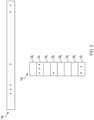
- FIG. 2illustrates an example of modifications made to page 118 1 and the distribution of the modifications among lines 22 of page 118 1 according to one or more embodiments.
- Page 118 1can include one of the pages 118 stored in storage 116 in FIG. 1 , and can include a range of data starting at a beginning logical address (e.g., a Logical Block Address (LBA)) to an ending logical address that corresponds to a predetermined page size, such as 4 KB.
- LBALogical Block Address
- modifications to data in page 118 1are made at various locations or positions in page 118 1 that are indicated with asterisks.
- the modifications in the example of FIG. 2are generally clustered or localized at three locations in the page. Aspects of the present disclosure take advantage of the tendency of updates or modifications to pages to be concentrated or clustered in the page by identifying one or more lines in the page that include data to be modified.
- the linescan be defined as a predetermined size or unit of data within the page.
- the predetermined size of the linescorresponds to a word size of processor circuitry requesting the modifications to the page.
- the word sizecan be the amount of data processed by the processor circuitry at a given time, such as 32 bits (i.e., 4 bytes) or 64 bits (i.e., 8 bytes), for example.
- page 118 1is divided into eight lines from line 22 0 to line 22 7 .
- Lines 22each have a predetermined size, such as 4 or 8 bytes, which would provide a total page size for page 118 1 of 32 or 64 bytes for eight lines from 22 0 to 22 7 .
- the predetermined size of the linescan vary in other implementations, and the number of lines shown FIG. 2 is for illustration purposes such that other implementations may include many more lines than the eight lines shown in FIG. 2 .
- page 118 1may include 4,096 bytes (i.e., a 4 KB page size) with 512 8B lines in some implementations.
- the line sizemay also be adjusted in the field based on changes in modification patterns or trends. For example, modification information, such as statistics on the clustering of modifications in pages may lead to an adjustment to a larger or smaller line size.
- modification informationsuch as statistics on the clustering of modifications in pages may lead to an adjustment to a larger or smaller line size.
- different hostsmay be associated with different line sizes, such that modification requests from a first host accessing DSD 108 result in a line size of 4 bytes, while modification requests from a second host result in a line size of 8 bytes.
- each modificationcan be a fixed unit of data, such as one byte.
- an encoding schemecan be selected for encoding the modifications to pages based on the degree of clustering of modifications within lines of one or more pages. Each encoding scheme may be associated with a different storage cost in terms of the storage space consumed in a cache (e.g., cache 12 A or cache 12 B in FIG. 1 ).
- the selected encoding schememay be reevaluated periodically, such as, for example, after a predetermined amount of time, a predetermined number of modifications, or a predetermined number of pages rewritten in the storage, to select a different encoding scheme if a lower storage cost is determined for the different encoding scheme.
- Thiscan allow for the encoding of modifications to adjust to different workloads or changing modification patterns caused by, for example, different applications 10 being executed at different times, or by different hosts accessing pages stored in the DSD.
- a number of lines with modifications in a pagemay need to be below a threshold number of lines before encoding and caching the modifications. If the threshold number of lines with modifications is reached, it may then be more efficient in terms of processing and memory resources to rewrite the page with the modifications without encoding and caching the modifications. On the other hand, if the threshold number of modified lines is not reached in such implementations, the modifications to the page may be considered sparse enough to accumulate encoded modifications for the page over time in a cache to defer rewriting the page. Such deferring of page rewrites can reduce the inefficiencies caused by write amplification, and prolong the usable life of the storage in cases where the storage has a limited write endurance.
- FIG. 3is an example of a system environment for modifying pages according to one or more embodiments.
- the modules shown in the example of FIG. 3may be implemented by, for example, processor circuitry 104 of host 101 or by controller circuitry 112 of DSD 108 in FIG. 1 .
- modification identifier module 30receives requests to modify pages stored in a non-volatile storage. Modification identifier module 30 may then access a mapping table (e.g., mapping table 14 A or 14 B in FIG. 1 ) to determine a cache status of the page and/or access information for the page.
- the mapping tablecan indicate a cache status of whether a page has modifications that have already been cached in the cache.
- the mapping tablecan include logical addresses (e.g., LBAs) for the pages that have modifications cached in the cache, a flag, or other identifier for pages that have modifications cached in the cache.
- Modification identifier module 30may alternatively or additionally access the mapping table in some implementations to determine access information for a page.
- the access informationmay indicate how recently a previous request to read or write data to the page occurred, and/or or a number of previous reads or writes to the page within a period of time.
- Modification identifier module 30may use the cache status and/or the access information for a page when receiving modification requests to determine whether to encode and cache the requested modifications or to rewrite the page without encoding and caching the requested modifications for the page.
- the requests to modify a pagecan include, for example, byte addresses for the data to be modified and the new data for the modification.
- Modification identifier module 30can identify the page using a mapping table (e.g., mapping table 14 A or 14 B in FIG. 1 ), and one or more lines in the page corresponding to the byte addresses for the modifications. Modification identifier 30 may also pass line positions indicating locations of the identified lines in the page to encoding module 34 if the modifications are to be cached, or may pass the line positions or byte addresses for the identified page to rewrite module 40 if the page is to be rewritten without caching the modifications.
- mapping tablee.g., mapping table 14 A or 14 B in FIG. 1
- modification identifier module 30may also provide encoding module 34 with one or more intra-line positions for each identified line indicating one or more locations for the modifications to be made in the line.
- modification identifier module 30may pass the new data for the modifications to encoding module 34 to create encoded data for the modifications.
- each of the line identification, the intra-line identification, and passing of new data for making the modificationsmay be handled by a separate module instead of by a single modification identifier module as shown in the example of FIG. 3 .
- Encoding module 34creates encoded data for the modifications, such as by encoding the line positions, intra-line positions, and new data using one of a plurality of different encoders, such as encoders 0 , 1 , 2 , and 3 in the example of FIG. 3 .
- Each encoderuses a different encoding scheme to encode the new data for the modifications and the associated location information for the modifications.
- some encoding schemesmay use the byte addresses for the modifications to encode the modifications as a delta list of modifications to be made to the page without taking into consideration line positions or intra-line positions for the modifications.
- Such an encoding schememay be used by encoder 0 for modification patterns that are considered to have low degree of clustering within one or more pages. An example of such an encoding scheme is discussed in more detail below with reference to FIG. 4B .
- encoding schemessuch as those used by encoders 1 , 2 , and 3 in FIG. 3 can be line-aware to take advantage of the clustering of modifications within lines, and to further reduce a storage cost for caching the modifications. Examples of such line-aware encoding schemes are discussed in more detail below with reference to FIGS. 4C, 4D, and 4E .
- some encoding schemessuch as those used by encoders 1 and 2 in FIG. 3 , can use a hierarchal line encoding that forms a tuple for each modified line including the line position, the intra-line position or positions of the modifications in the line, and the new data for making the modifications in the line. Examples of such hierarchal line encoding are discussed in more detail below with reference to FIGS. 4C and 4D .
- Another type of line-aware encodingcan be performed by encoder 3 in FIG. 3 to map the modifications to a page and perform entropy encoding, such as Huffman encoding or arithmetic encoding, on one or more bit sequences derived from the modification mapping and the associated new data.
- entropy encodingsuch as Huffman encoding or arithmetic encoding
- the encoder or encoding scheme used to create encoded data for the modifications and the location information associated with the modificationsis selected by selector module 32 based on storage costs determined for using different encoding schemes for one or more pages and/or collected modification information that may indicate a degree of clustering of modifications.
- the determined storage costscan relate to a degree of clustering of modifications within the lines identified by modification identifier 30 .
- Different encoding schemescan have different storage costs relative to each other in terms of the amount of storage consumed in the cache depending on the level or degree that modifications are clustered in the contiguous byte ranges forming the identified lines.
- selector module 32can periodically determine storage costs for one or more pages that receive one or more page modification requests at modification identifier module 30 , as indicated by the dashed line from modification identifier module 30 and selector module 32 .
- the sampling of modification requestsmay occur, for example, after a predetermined period of time since a previous selection of an encoding scheme, after a predetermined number or modification requests, and/or after a predetermined number of pages have been rewritten in the storage of the DSD.
- modification identifier module 30may provide a copy of the information provided to encoder module 34 for encoding using the currently selected encoding scheme.
- the other encoders of encoder module 34may then encode the same modifications and associated location information for selector module 32 to compare storage costs for the different encoding schemes.
- modification requests for multiple pagesmay be used to determine average storage costs for each of the different encoding schemes for comparison.
- the storage costs for modifications to a single pagemay be compared.
- Selector module 32may then select the encoding scheme or encoder that results in the lowest storage cost for the modifications for the one or more pages.
- selector module 32may additionally or alternatively select an encoding scheme based on modification information that may be collected by modification identifier module 30 .
- modification informationmay include, for example, statistics such as an average number of modifications for each modified line divided by the number of modifications being made to a page.
- the collected informationcan include the number of modifications made within different byte ranges of each other, such as the number of modifications made within 4 bytes, 8 bytes, and 16 bytes of another modification. The number of modifications made within these different byte ranges may then be divided by the number of modifications for a page to determine a degree of clustering for the modifications using the different sized byte ranges.
- Such different sized byte rangesmay correspond to different possible line sizes that could be used for encoding modifications.
- Selector module 32may then select an encoding scheme based on a threshold value for the collected modification information, such that the collected modification information (e.g., an average number of modifications per modified line) is within a threshold for a particular encoding scheme.
- encoding scheme 1may be associated with a threshold of an average of 1.1 modifications per modified line
- encoding scheme 2may be associated with a threshold of an average of 1.3 modifications per modified line.
- selector module 32can select encoding scheme 2 when the collected modification information indicates an average number of modifications per modified line of 1.2.
- selector module 32may select an encoding scheme by changing the line size used for encoding to better suit the degree of clustering indicated by the collected modification information.
- the encoded modifications and location information for the selected encoding schemeare cached by caching module 36 in a cache that is managed by caching module 36 .
- caching module 36can implement caching policies for the cache, such as determining when to flush data from the cache and/or which data to flush from the cache.
- cache module 36may determine that a remaining available storage space or the amount of cached data has reached a storage threshold for flushing data from the cache.
- cache module 36may determine that an access threshold, such as a write frequency and/or a read frequency, for a particular page that has modifications stored in the cache has fallen below a threshold access frequency. In such implementations, cache module 36 may then flush the modifications for less frequently read and/or less frequently written pages from the cache to make room for caching modifications for more frequently read and/or more frequently written pages. Caching data for more frequently read and/or more frequently written pages may provide a performance benefit in some implementations, since it may be quicker to access such data from the cache than from the non-volatile storage (e.g., storage 116 in FIG. 1 ).
- an access thresholdsuch as a write frequency and/or a read frequency
- the access thresholdmay also include, or may alternatively include, how recently data for the page has been accessed, so that encoded data for pages that have been more recently accessed (e.g., written to and/or read from within a predetermined period of time) are kept in the cache longer than encoded data for pages that have less recently been accessed.
- updates or modifications for pagescan be accumulated in the cache before flushing the updates or modifications for the page to be rewritten in the storage.
- Cache module 36may access a mapping table (e.g., mapping table 14 A or mapping table 14 B in FIG. 1 ) to determine access information for a page that has modified data in the cache. Cache module 36 in some implementations may also update the access information in the mapping table, such as to increment a modification count or an overall access count for a page, for example. In some implementations, cache module 36 may also access the mapping table to determine whether modifications to be cached should overwrite previously cached modifications for the page.
- a mapping tablee.g., mapping table 14 A or mapping table 14 B in FIG. 1
- Decoder module 38decodes the data flushed from the cache for rewriting the corresponding page with the new data in storage 116 .
- decoder module 38may be used for decoding modified data that has been requested by processor circuitry of a host. As shown in FIG. 3 , decoder module 38 includes decoders 0 to 3 corresponding to respective encoders 0 to 3 for decoding the encoded data based on the encoding scheme used to encode the data.
- the encoded datamay include an indication of the encoding scheme used to encode the data, such as with a first value for the encoded data.
- a mapping table(e.g., mapping table 14 A or 14 B in FIG. 1 ) may indicate the encoding scheme used to encode the data.
- Rewrite module 40performs read-modify-write operations for storage of modified pages in the storage of the DSD.
- the processor circuitry of the hoste.g., processor circuitry 104 in FIG. 1
- the processor circuitrycan use rewrite module 40 to request the old page stored in the storage of the DSD, and update the page in the host's main memory (e.g., main memory 106 in FIG. 1 ) with the decoded modified data before sending a write command to the DSD using a block interface to write the new page with the modified data to replace the obsolete version of the page in the storage.
- the controller circuitry of the DSDe.g., controller circuitry 112 in FIG.
- the controller circuitrycan use rewrite module 40 to request the old page stored in the storage of the DSD, and update the page in a memory of the DSD (e.g., memory 114 in FIG. 1 ) with the decoded modified data before writing the new page with the modified data to replace the obsolete version of the page in the storage.
- a memory of the DSDe.g., memory 114 in FIG. 1
- implementationsmay include a different system environment than shown in FIG. 1 .
- other implementationsmay include different modules, such as separate line identifier and intra-line identifier modules in place of modification identifier module 30 , or a combined encoding and decoding module in place of encoding module 34 and decoding module 38 .
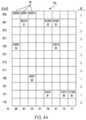
- FIG. 4Aillustrates modifications for page 118 2 according to one or more embodiments.
- page 118 2is to be modified with new data B 1 to B 9 at various locations throughout page 118 2 .
- page 118 2has been divided into twelve lines shown as rows in FIG. 4A . Each line includes eight positions, with each position shown as a separate box in FIG. 4A . Each position in the example of FIG. 4A represents one byte of data, such that page 118 2 has a page size of 96 bytes.
- this page sizeis only for purposes of illustration, and that page sizes in practice will generally be much larger than page 118 2 in FIG. 4A , such as for pages including, for example, 4,096 bytes that are logically divided into 512 lines of eight bytes.
- modificationsare to be made to data in four out of the twelve lines of page 118 2 .
- the new data B 1 to B 9represent data that is to replace data currently stored in page 118 2 in a storage of a DSD (e.g., storage 116 in FIG. 1 ).
- FIGS. 4B to 4E discussed belowdescribe different example encoding schemes that have different storage costs for caching the modifications and the associated location information for the modifications in a cache.
- the references in FIG. 4A to “ 4 B”, “ 4 C”, “ 4 D”, and “ 4 E”refer to encoding used to identify positions of modifications in page 118 2 , and are discussed in more detail below.
- FIG. 4Billustrates a first example encoding scheme referred to herein as a delta list encoding scheme for creating encoded data for the modifications shown in FIG. 4A according to one or more embodiments.
- the delta list encoding scheme of FIG. 4Bmay be performed by, for example, encoder 0 in FIG. 3 discussed above.
- the modifications and the associated location informationare encoded as a list of nine tuples, with each tuple including a location in page 118 2 for the modification, and the new data for the modification (e.g., B 1 for the first modification).
- each boxi.e., each byte or unit in page 118 2
- the location for modification B 1occurs at a location represented by 0001010.
- the first tuple for the first modificationincludes the page location of 0001010 and data for B 1 .
- B 2 to B 9each have their own tuple in the list including the seven bit location for the modification, and the data for the modification.
- the number of bits needed to uniquely represent the location of each modificationwill depend on the size of the page (e.g., a 4 KB page size) and a unit size for each modification (e.g., a 1 byte modification size).
- the storage cost for a delta list encoding schemedepends on the number of modifications made to the page, the size of the units or modifications, and the number of bits needed to represent each position in the page for a given page size and unit size.
- a storage cost, S 0 , for the delta list encodingcan be represented in terms of the number of modifications (m), the size of the page (pagesize), and the size of the units (unitsize), as shown in Equation 1 below.
- a 4 KB page sizewould have a pagesize of 32,768 bits (i.e., 4,096 bytes multiplied by 8 bits), and a 1 byte unit size would have a unitsize of 8 bits.
- the storage cost S 0is m(12+8) bits, or 20m bits.
- the log 2 portion of the factor of mi.e., 12
- the remaining portion of the factor of mi.e., 8) is the number of bits needed to represent the modified data (e.g., B 1 ).
- the encoded modifications and location informationcan be cached (e.g., in cache 12 A or cache 12 B in FIG. 1 ), and a mapping table (e.g., mapping table 14 A or mapping table 14 B) can be updated to indicate that modified data for page 118 2 is in the cache.
- a decoder for delta list encodingsuch as decoder 0 in FIG. 3
- decoder 0 in FIG. 3can decode the encoded modifications for rewriting page 118 2 in a storage (e.g., storage 116 in FIG. 1 ) including the modifications (i.e., B 1 to B 9 ).
- the cached data for the modifications or the mapping tablecan include an indication of which encoding scheme was used to encode the data so that the correct decoder is used.
- FIG. 4Cillustrates a second example encoding scheme referred to herein as an intra-line list encoding scheme for creating encoded data for the modifications shown in FIG. 4A according to one or more embodiments.
- the intra-line list encoding scheme of FIG. 4Cmay be performed by, for example, encoder 1 in FIG. 3 discussed above.
- the intra-line list encoding scheme of FIG. 4Cdiffers from the delta list encoding scheme of FIG. 4B in that the intra-line list encoding scheme is line-aware by using a hierarchal encoding based on the logical divisions of page 118 2 into lines of contiguous byte ranges.
- each row or line in page 118 2is assigned a binary line position under the reference for “ 4 C & 4 D” on the left of page 118 2 from 0000 for the first line at the top of page 118 2 to 1100 for the twelfth line at the bottom of page 118 2 .
- line-aware encodingcan take advantage of processing patterns that tend to make modifications to data within a logical proximity of other modifications (i.e., clustered modifications).
- FIG. 4Conly four of the twelve lines in page 118 2 are to be modified. The other eight lines therefore do not need encoding in the example encoding of FIG. 4C .
- Each of the four modified linesis represented in the encoding with its binary line position (e.g., 0001 for the first modified line).
- a list of one or more tuplesthen follow the line position, with each tuple including an intra-line position for a modification in the line, and the modified data.
- the first modified line identified by the line position 0001includes three tuples for modifications to be made for B 1 , B 2 , and B 3 . Since there are 8 bytes per line in the example of page 118 2 in FIG. 4A , three bits are used to represent an intra-line position for each modification.
- the first modification of B 1 in the first modified line in FIG. 4Ahas an intra-line position of 001.
- the second modification of B 2 in the first modified linehas an intra-line position of 100.
- the third modification of B 3 in the first modified linehas an intra-line position of 101.
- modifications after the first modification for a lineinclude a new intra-line unit indicator to denote that there is another modification in the same line.
- a 0precedes the intra-line positions for B 2 and B 3 to indicate a new modification in the same line so that the line position of 0001 is only provided once for all three modifications of B 1 , B 2 , and B 3 in the first modified line.
- the line position for the second modified line, and the line positions for all modified lines after the first modified lineis preceded by a 1 to indicate a new line.
- a 1precedes the line position of 0100 for the second modified line to indicate a new modified line after the first modified line.
- the first modified linedoes not need a new line identifier in the example of FIG. 4C .
- the storage cost for an intra-line list encoding schemedepends on the number of modifications made to the page, the size of the units or modifications, the number of bits needed to represent the position of each line in the page for a given page size and line size, and the number of bits needed to represent each intra-line position for a given line size and unit size.
- a storage cost, S 1 , for the intra-line list encodingcan be represented in terms of the number of modifications (m), the size of the page (pagesize), the size of the lines (linesize), the size of the units (unitsize), and the number of modified lines (M), as shown in Equation 2 below.
- a 4 KB page sizewould have a pagesize of 32,768 bits
- an 8 byte line sizewould have a linesize of 64 bits
- a 1 byte unit sizewould have a unitsize of 8 bits.
- the storage cost S 1is (1+9)M ⁇ 1+(3)M+(1+3)(m ⁇ M)+8m, which reduces to 9M+12m ⁇ 1.
- the first addend in Equation 2 aboverepresents the storage cost in bits for encoding the line positions of each modified line, with the number of bits needed to uniquely represent each line based on the pagesize and linesize, and an additional bit to indicate each modified line after the first modified line (e.g., the 1 preceding each modified line's position after the first modified line in FIG. 4C ). An extra bit is subtracted out for the first modified line, which does not need a new line indicator, as in the example of FIG. 4C .
- the second addend in Equation 2represents the storage cost in bits of the first modification made in each modified line
- the third addendrepresents the storage cost of each modification made in each modified line after the first modification.
- the last addendrepresents the storage cost of the modified data (e.g., the storage cost for B 1 to B 9 ), which is the same as in the delta list encoding example of FIG. 4B .
- the intra-line list encoding schemeprovides less compression than the delta encoding scheme for pages with more than one modification.
- the encoded datacan be cached, and a mapping table can be updated to indicate that modified data for page 118 2 is cached in the cache.
- a decoder for intra-line list encodingsuch as decoder 1 in FIG. 3
- the cached data for the modifications or the mapping tablecan include an indication of which encoding scheme was used to encode the data so that the correct decoder is used.
- FIG. 4Dillustrates a third example encoding scheme referred to herein as an intra-line bitmap encoding scheme for creating encoded data for the modifications shown in FIG. 4A according to one or more embodiments.
- the intra-line bitmap encoding scheme of FIG. 4Dmay be performed by, for example, encoder 2 in FIG. 3 discussed above.
- the intra-line bitmap encoding scheme of FIG. 4Dis line-aware by using a hierarchal encoding based on the logical divisions of page 118 2 in FIG. 4A into lines of contiguous byte ranges.
- the intra-line bitmap encoding scheme of FIG. 4Ddiffers from the intra-line list encoding scheme of FIG. 4C in that the intra-line bitmap encoding scheme uses a line modification bitmap for each modified line instead of a separate position for each modification.
- each line in page 118 2is assigned a binary line position shown in FIG. 4A under the reference for “ 4 C & 4 D” on the left of page 118 2 .
- the line positionsbegin with 0000 for the first line at the top of page 118 2 to 1100 for the twelfth line at the bottom of page 118 2 .
- line-aware encodingcan take advantage of processing patterns that tend to make modifications to data within a logical proximity of other modifications (i.e., clustered modifications). In the example of FIG. 4D , only four of the twelve lines in page 118 2 are to be modified. The other eight lines therefore do not need encoding in the example of FIG. 4D .
- each of the four modified linesis represented in the encoding scheme of FIG. 4D with its binary line position (e.g., 0001 for the first modified line).
- a bitmap representing each unit in the modified linefollows the line position in FIG. 4D to provide intra-line positions for the modifications.
- a value of 1 in the bitmapindicates the position of a modification in the line
- a value of 0 in the bitmapindicates no change for the corresponding position in the line.
- the line modification bitmap for the first modified line in the example encoding of FIG. 4Dindicates modifications at the second, fifth, and sixth locations in the line with the bitmap [01001100].
- the data for the modified positionsthen follows the bitmap with B 1 , B 2 , and B 3 .
- each modified line in the intra-line bitmap encodingrequires a bitmap including a number of bits equal to the number of units in a line (e.g., eight bits for the eight units per line in FIG. 4A ), greater compression can typically be achieved when there is a greater degree of clustering of modifications within lines than when using intra-line list encoding because each modification does not need a separate intra-line position or additional boundary encoding, such as extra bits to indicate new modifications within the same line or an extra bit to indicate the start of a new line.
- the storage cost for an intra-line bitmap encoding schemedepends on the number of modifications made to the page, the size of the units or modifications, the number of bits needed to represent the position of each line in the page for a given page size and line size, and the number of bits needed in a bitmap for a given line size and unit size.
- a storage cost, S 2 , for the intra-line bitmap encodingcan be represented in terms of the number of modifications (m), the size of the page (pagesize), the size of the lines (linesize), the size of each unit (unitsize), and the number of modified lines (M), as shown in Equation 2 below.
- a 4 KB page sizewould have a pagesize of 32,768 bits
- an 8 byte line sizewould have a linesize of 64 bits
- a 1 byte unit sizewould have a unitsize of 8 bits.
- the storage cost S 2is (9+8)M+8m, which reduces to 17M+8m.
- the first addend in Equation 3 above(i.e., the loge portion) represents the storage cost in bits for encoding the line positions of each modified line, with the number of bits needed to uniquely represent each line based on the pagesize and linesize.
- the second addend in Equation 3(e.g., (linesize/unitsize) ⁇ M) represents the storage cost in bits of the intra-line modification bitmap.
- the last addendrepresents the storage cost of the modified data (e.g., B 1 ), which is the same as in the delta list and intra-line list encoding examples discussed above.
- the amount of compression for the intra-line bitmap encoding of FIG. 4Dis typically greater when there is more clustering of modifications in lines, but less when there is a minimal degree of clustering.
- the storage cost S 2 for the intra-line bitmap encoding schemeis 25m.
- the encoded datacan be cached, and a mapping table can be updated to indicate that modified data for page 118 2 is cached in the cache.
- a decoder for intra-line bitmap encodingsuch as decoder 2 in FIG. 3 , can decode the encoded modifications for rewriting page 118 2 in the storage including the modifications (i.e., B 1 to B 9 ).
- the cached data for the modifications or the mapping tablecan include an indication of which encoding scheme was used to encode the data so that the correct decoder is used.
- FIG. 4Eillustrates a fourth example encoding scheme referred to herein as a modification mapping entropy encoding scheme for creating encoded data for the modifications shown in FIG. 4A according to one or more embodiments.
- the encoding scheme of FIG. 4Emay be performed by, for example, encoder 3 in FIG. 3 discussed above.
- the modification mapping entropy encoding scheme of FIG. 4Eis line-aware by using the logical divisions of page 118 2 of FIG. 4A into lines of contiguous byte ranges.
- the encoding scheme of FIG. 4Ediffers from the intra-line list and intra-line bitmap encoding schemes discussed above in that the modification mapping of FIG. 4E generates a bit sequence mapping the lines that have been modified and the lines that have not been modified in the page, before entropy encoding the bit sequence for the line modifications with bit sequences for each modified line.
- each line in page 118 2is assigned either a 1 or a 0 on the right side of page 118 2 to indicate whether the line is to be modified.
- line-aware encodingcan take advantage of processing patterns that tend to make modifications to data within a proximity of other modifications (i.e., clustered modifications).
- the locations of the modified lines in the pageare encoded with a bitmap.
- Each line that has a modificationhas a 1 value, while each line that is not modified has a 0 value.
- This bitmapis fed as a bit sequence into encoder 3 in FIG. 4E to produce an encoded line sequence.
- Encoder 3can use an entropy encoding, such as Huffman encoding or arithmetic encoding, for example.
- the modifications in each modified lineare mapped into a modified line bit sequence that includes the intra-line positions for the modifications.
- the first modified line sequenceindicates a value of 0 for the first unit in the first modified line to indicate no modification to the first unit, but a value of 1 for the second unit to indicate a modification at the second unit, as shown in FIGS. 4A and 4E .
- the data for the modificationfollows with B 1 .
- the next modification in the first modified lineis indicated after two 0 values for no changes at the third and fourth units, before a value of 1 indicating a modification at the fifth unit in the line.
- the data for the second modification at the fifth unitfollows with the new data for the second modification, B 2 .
- a value of 1follows B 2 in the modified line sequence to indicate a third modification at the sixth unit in the line, which is followed by the new data for the modification, B 3 .
- the line sequence indicating which lines have been modified in the page, and each of the four modified line sequencesare input into encoder 3 , which performs entropy encoding, such as Huffman encoding or arithmetic encoding.
- encoder 3uses a line distribution of modified lines to other lines in page 118 2 to encode the line sequence.
- the line distributionis 1 ⁇ 3, since four out of the twelve lines have been modified.
- the encoded line sequence generated by encoder 3further compresses the line sequence to take up less space in the cache.
- Each of the four modified line sequencesare also encoded by encoder 3 using a respective intra-line distribution for encoding the intra-line modification position or positions and the associated new data (e.g., B 1 , B 2 , and B 3 for the first modified line).
- the sequences encoded by encoder 3can be encoded as separate streams or as one stream fed to encoder 3 .
- the line sequence and the modified line sequences in some implementationscan be arranged as a single sequence.
- the line sequence in FIG. 4Ecan be interleaved with the modified line sequences to form the sequence: 01 01B1001B216300 001 1B400001B500 0001 001B600000 01 00001B701B81B9 0 , with the underlined portions in the sequence taken from the line sequence, and the portions following each “1” in the underlined portions of the line sequence being the modified line sequences corresponding to the underlined “1.”
- a dictionarymay be stored in a memory (e.g., main memory 106 or memory 114 in FIG. 1 ) to replace portions of the sequence input into the encoder with varying length sequences based on the frequency that the portion of the sequence appears in the sequence.
- Arithmetic encodingdoes not need to store a dictionary, and can usually provide more compression for longer sequences than Huffman encoding.
- the storage cost for the pre-processing modification mapping before entropy encodingdepends on the number of modifications made to the page, the size of the units or modifications, and the number of lines in the page.
- a storage cost, S 3 , for the page modification mapping in FIG. 4E before entropy encodingcan be represented in terms of the number of modifications (m), the size of the page (pagesize), the size of the lines (linesize), the size of each unit (unitsize), and the number of modified lines (M), as shown in Equation 4 below.
- a 4 KB page sizewould have a pagesize of 32,768 bits
- an 8 byte line sizewould have a linesize of 64 bits
- a 1 byte unit sizewould have a unitsize of 8 bits.
- the storage cost S 3is 512+8M+8m. This storage cost is typically further reduced by the entropy encoding performed by encoder 3 in the example of FIG. 4E .
- the first addend in Equation 4 aboverepresents the storage cost in bits for the line sequence as a bitmap including one bit for each line in the page.
- the second addend in Equation 4represents the storage cost in bits for the modified line sequences as bitmaps.
- the last addendrepresents the storage cost of the modified data (e.g., B 1 to B 9 ), which is the same as in the encoding examples discussed above for FIGS. 4B to 4D .
- the encoded modificationscan be cached, and a mapping table can be updated to indicate that modified data for page 118 2 is cached in the cache.
- a decoder for decoding the modification mapping encoding and entropy encoding of FIG. 4Esuch as decoder 3 in FIG. 3 , can decode the encoded modifications for rewriting page 118 2 in the storage including the modifications (i.e., B 1 to B 9 ).
- the cached data for the modifications or the mapping tablecan include an indication of which encoding scheme was used to encode the data so that the correct decoder is used.
- any of the foregoing encoding schemes discussed above for the delta list encoding scheme of FIG. 4B , the intra-line list encoding scheme of FIG. 4C , or the intra-line bitmap encoding scheme of FIG. 4Dcan be modified to include further entropy encoding as in the encoding scheme of FIG. 4E .
- the encoded sequence for FIG. 4D including the intra-line bitmapscan be further compressed or encoded using entropy encoding before storing the encoded modifications and associated location information in a cache.
- changes to the disclosed encoding schemesare possible, such as by combining different aspects of some or all of the example encoding schemes described above for FIGS. 4B to 4E .
- FIG. 5is a flowchart for a line-aware modification caching process according to one or more embodiments.
- the modification caching process of FIG. 5may be performed, for example, by processor circuitry 104 or controller circuitry 112 in FIG. 1 executing modification identifier module 30 , encoding module 34 , and cache module 36 of FIG. 3 .
- the circuitryreceives one or more requests to modify data stored in a page (e.g., a page 118 in FIG. 1 ) in non-volatile storage (e.g., storage 116 in FIG. 1 ) with new data.
- the one or more requestsmay come from a processor executing an application that has modified or updated data for a page in its main memory (e.g., main memory 106 in FIG. 1 ).
- a processor of the host's processor circuitrymay execute an application that modifies the data, and stores the modified data in the host's main memory, which may serve as the request or requests to modify the data stored in the page in the non-volatile storage.
- the hostcan use a block interface for communicating with the DSD including the storage when the page is ready to be rewritten with the new data.
- a processor of the host's processor circuitrymay execute an application that modifies the data.
- the hostmay then use a memory interface to send the one or more requests to the DSD, which are received by the controller circuitry of the DSD as one or more page modification requests.
- the circuitryidentifies one or more lines in the page that include data to be modified by the one or more requests.
- the identification of lines to be modifiedmay be performed by executing a modification identifier module, such as modification identifier module 30 in FIG. 3 .
- the linescan include logical divisions of the page into contiguous byte ranges of a predetermined size, such as 8 byte lines, for example.
- a line position identifieras in the line-aware encoding schemes of FIGS. 4C and 4D , or a line bitmap, as in the modification mapping of FIG. 4E , may be used to identify the line position of the modified line or lines.
- the line sizemay depend on recently collected modification information to better suit recent modification patterns that may result from a particular application or host.
- the circuitrymay associate the host requesting the modification with a particular line size, which may be based on previously collected modification information for requests sent by the host or information about the host's processor circuitry, such as a word size used by a processor of the host.
- the circuitrydetermines whether the number of lines identified in block 504 with modifications is greater than or equal to a threshold number of lines.
- encoding and caching modifications for the pagemay not be efficient or worthwhile in terms of performance and/or storage space available in the cache if more than the threshold number of lines are to be modified in the page.
- the circuitry in block 508rewrites the page in the non-volatile storage including the new data without encoding at least the line positions and intra-line positions.
- the modified datamay still be temporarily cached as part of the normal page writing process without using a line-aware encoding scheme.
- the rewritingmay be performed by processor circuitry of the host by requesting the page from the storage, modifying the page in the host's main memory to include the new data, and sending a write command to the DSD to write the modified page in place of the obsolete page in the storage.
- the host and DSD in such implementationsmay communicate using a block or storage device interface.
- the rewritingmay be performed by controller circuitry of the DSD by modifying the page in a memory of the DSD and rewriting the page with the new data in the storage.
- the host and DSDin such embodiments may communicate using a memory device interface.
- the circuitry in block 510creates encoded data based on the new data and respective locations of the one or more identified lines in the page. This can include encoding a line position, the new data, and one or more intra-line positions for each modified line identified in block 504 .
- the circuitrymay execute an encoding module, such as encoding module 34 in FIG. 3 .
- the circuitrymay use a line-aware encoding scheme previously selected based on a degree of clustering of modifications to one or more other pages stored in the storage.
- Such line-aware encoding schemescan include, for example, the intra-line list encoding scheme of FIG. 4C , the intra-line bitmap encoding scheme of FIG. 4D , or a modification mapping entropy encoding scheme that uses a line mapping as in FIG. 4E .
- the use of such line-aware encoding schemescan reduce the storage size of the encoded modifications for caching when there is a relatively higher degree of clustering of modifications, as compared to a delta list encoding scheme or other encoding scheme that does not consider the proximity of modifications in the page.
- the circuitrycaches the encoded data created in block 510 in a cache (e.g., cache 12 A or cache 12 B in FIG. 1 ).
- the encoded data, or a portion thereof,can then be used at a later time to rewrite the page in the storage with the new data to reduce write amplification that would otherwise result from rewriting the page for each request to modify the page.
- the circuitrymay execute a caching module, such as caching module 36 in FIG. 3 , to cache the encoded modifications.
- the circuitry in block 512may update a mapping table (e.g., mapping table 14 A or mapping table 14 B in FIG. 1 ) to indicate which data has been modified and cached for the page. New requests to modify the same data may then result in encoded modifications that replace the previously cached modifications in the cache.
- FIG. 6is a flowchart for a page rewrite process according to one or more embodiments.
- the page rewrite process of FIG. 6may be performed, for example, by processor circuitry 104 or controller circuitry 112 in FIG. 1 executing cache module 36 , decoder module 38 , and rewrite module 40 of FIG. 3 .
- a cache memory thresholdcan include, for example, a threshold amount of data stored in the cache or a threshold amount of available storage remaining in the cache.
- the access thresholdcan include, for example, a number of access requests (e.g., read or write requests) for a page within a predetermined amount of time, and/or a predetermined amount of time since a page last received an access request.
- the flushing of encoded data from the cachemay or may not be specific to a particular page. For example, one implementation may flush encoded data from the cache for all pages that have not been modified within a predetermined period of time in response to reaching a cache memory threshold. In another example, the circuitry may flush the encoded data for all pages in response to reaching a cache memory threshold. Other cache policies may include flushing encoded data for pages that have reached an access threshold, regardless of the storage available in the cache or the size of the cached data.
- the circuitrydecodes at least a portion of the encoded new data in the cache for one or more pages stored in the non-volatile storage in response to the cache memory threshold and/or the access threshold being reached in block 602 .
- the circuitrymay execute a decoding module (e.g., decoding module 38 in FIG. 3 ) that decodes the encoded modified data and associated encoded location information.
- the circuitrymay access a mapping table to determine which decoder or decoding scheme to use to decode the encoded data.
- the decoded datamay, for example, be temporarily stored in a memory accessed by the circuitry (e.g., main memory 106 or memory 114 in FIG. 1 ) for combining with the valid data read from the storage for the page, before rewriting the page with the new data.
- the circuitryrewrites the one or more pages in the non-volatile storage including at least a portion of the new data for the one or more pages.
- some or all of the encoded modifications in the cache for a pagemay be overwritten while still in the cache.
- the new modificationsmay overwrite the old modifications such that only a portion of the modifications in the cache (i.e., the new modifications) are included in the rewritten page in the storage.
- the circuitrymay execute a rewrite module (e.g., rewrite module 40 in FIG. 3 ) for rewriting the page including the new data for the modifications.
- the hostmay rewrite the page by first reading the page from the DSD, and modifying the page in its main memory, before sending a write command to the DSD to rewrite the page with the new data.
- Such an operationcan be referred to as a page swap operation or read-modify-write operation performed by the host.
- the DSDmay rewrite the page by first reading the page from the storage, and modifying the page in a local memory of the DSD, before rewriting the page in the storage with the new data.
- Such an operationcan be referred to as a read-modify-write operation of the DSD.
- FIG. 7is a flowchart for an encoding selection process according to one or more embodiments.
- the encoding selection process of FIG. 7may be performed, for example, by processor circuitry 104 or controller circuitry 112 in FIG. 1 executing selector module 32 of FIG. 3 .
- the circuitrydetermines storage costs for using different respective encoding schemes to create encoded data for one or more pages.
- different encoding schemescan have different storage costs in terms of the storage size or compression ratio achieved depending on a degree of clustering of the modifications in a page.
- the circuitrymay periodically analyze or sample modifications made to one or more pages stored in the storage to determine a storage cost, and evaluate whether to change a current encoding scheme to a different encoding scheme based on recent modification patterns.
- the circuitryselects an encoding scheme that has the lowest storage cost determined in block 702 for the one or more pages.
- line-aware encoding schemessuch as the intra-line list encoding scheme of FIG. 4C , the intra-line bitmap encoding scheme of FIG. 4D , or the modification mapping entropy encoding scheme of FIG. 4E may be selected over a non-line-aware encoding scheme, such as the delta list encoding scheme of FIG. 4B .
- the selected encoding schememay then be used for a predetermined period of time or until a different encoding evaluation trigger is reached.
- a host or application that sends one or more requestsmay indicate an encoding scheme to be used for the modifications. For example, an application may send a request to modify a page with a high degree of clustering and indicate that a particular line-aware entropy encoding should be used. Such an indication can include, for example, logical addresses that are associated with more or less clustering of modifications, or a value included with the request.
- the circuitry in block 710selects an encoding scheme for encoding the requested modifications based on the received indication.
- the example process of FIG. 7proceeds to block 708 to wait until one or more encoding scheme evaluation triggers are reached.
- the circuitrymay revert back to the previously used encoding scheme after creating encoded data for the modifications of the request using the indicated encoding scheme.
- the circuitrymay continue using the indicated encoding scheme until changed after reaching one or more evaluation triggers.
- encoding evaluation triggerscan include, for example, reaching a predetermined time since a previous evaluation of encoding schemes, reaching a predetermined number of modifications to pages since a previous evaluation of encoding schemes, or reaching a predetermined number of rewritten pages in the storage since a previous evaluation of encoding schemes. Some implementations may reevaluate the encoding schemes upon reaching one evaluation trigger, while other implementations may require multiple evaluation triggers to be reached before reevaluating the encoding schemes. When such an evaluation trigger or evaluation triggers are reached, the process returns to block 702 to determine storage costs for using the different encoding schemes with a recent modification request or modification requests.
- FIG. 8is a flowchart for another encoding selection process according to one or more embodiments.
- the encoding selection process of FIG. 8may be performed, for example, by processor circuitry 104 or controller circuitry 112 in FIG. 1 executing selector module 32 of FIG. 3 .
- one or more evaluation triggersare reached for evaluating the current encoding scheme.
- Such encoding evaluation triggerscan include, for example, reaching a predetermined time since a previous evaluation of encoding schemes, reaching a predetermined number of modifications to pages since a previous evaluation of encoding schemes, or reaching a predetermined number of rewritten pages in the storage since a previous evaluation of encoding schemes.
- the circuitrycollects modification information from a plurality of requests to modify pages stored in a non-volatile storage (e.g., storage 116 in FIG. 1 ).
- the modification informationmay be collected for a predetermined number of modification requests or for a predetermined number of pages, for example.
- the modification informationmay be collected by a modification identification module executed by the circuitry, such as modification identification module 30 in FIG. 3 .
- the collected modification information in some implementationscan indicate a degree of clustering of modifications.
- the collected modification informationcan include statistics such as an average number of modifications for each modified line divided by the number of modifications being made to the page.
- the collected informationcan include the number of modifications made within different byte ranges of each other, such as the number of modifications made within 4 bytes, 8 bytes, and 16 bytes of another modification. The number of modifications made within these different byte ranges may then be divided by the number of modifications for the page to determine a degree of clustering for the modifications using the different sized byte ranges. Such different sized byte ranges may correspond to different possible line sizes that could be used for encoding modifications.
- the circuitryselects an encoding scheme (e.g., one of encoding schemes 0 , 1 , 2 , or 3 discussed above) based on the collected modification information.
- each encoding schememay be associated with a threshold such that the collected information (e.g., an average number of modifications per modified line) may fall within a threshold for a particular encoding scheme.
- the circuitrymay select an encoding scheme by changing the line size used for encoding to better suit the degree of clustering indicated by the collected modification information.
- the encoding selection process of FIG. 8may differ in other implementations.
- other implementationsmay allow for a temporary or ongoing selection of an encoding scheme based on an indication received from a host, as with blocks 706 and 710 discussed above for the example of FIG. 7 .
- aspects of the encoding selection processes of FIGS. 7 and 8may be combined in some implementations, such that the selection of an encoding scheme can be made based on collected modification information and/or determined storage costs.
- the encoding and caching of modifications to pages stored in a non-volatile storagecan reduce a write amplification in the non-volatile storage.
- the reduction in write amplificationcan ordinarily reduce an overall use of processing and memory resources that may otherwise be needed to perform multiple read-modify-write operations to rewrite pages for only a relatively small proportion of new data.
- This deferral of rewriting pages in the storagecan also save time in terms of Input/Output (I/O) performance, and reduce the wear on storage that may have a limited write endurance.
- I/OInput/Output
- line-aware encoding schemesto create encoded data based on respective locations of modified lines in a page can ordinarily allow for more modifications to be accumulated in a cache to further reduce the frequency of rewriting pages.
- line-aware encoding schemescan provide greater compression for modifications due to the tendency of applications to make modifications within close proximity to other modifications in the page.
- a general-purpose processormay be a microprocessor, but in the alternative, the circuitry may be any conventional processor circuitry, controller circuitry, microcontroller circuitry, or state machine.
- Processor circuitry or controller circuitrymay also be implemented as a combination of computing devices, e.g., a combination of a DSP and a microprocessor, a plurality of microprocessors, an SoC, one or more microprocessors in conjunction with a DSP core, or any other such configuration.
- a software modulemay reside in RAM memory, flash memory, ROM memory, EPROM memory, EEPROM memory, registers, hard disk, a removable media, an optical media, or any other form of storage medium known in the art.
- An exemplary storage mediumis coupled to the processor circuitry or controller circuitry such that the circuitry can read information from, and write information to, the storage medium.
- the storage mediummay be integral to processor circuitry or controller circuitry.
- the circuitry and the storage mediummay reside in an ASIC or an SoC.
Landscapes
- Engineering & Computer Science (AREA)
- Theoretical Computer Science (AREA)
- Physics & Mathematics (AREA)
- General Engineering & Computer Science (AREA)
- General Physics & Mathematics (AREA)
- Software Systems (AREA)
- Human Computer Interaction (AREA)
- Information Retrieval, Db Structures And Fs Structures Therefor (AREA)
Abstract
Description
where pagesize and unitsize are expressed in bits. For the example of a 4 KB page size and 1 byte modification unit size, there is a storage savings if m, the number of modifications in a page, is less than 1,638 modifications.
Claims (24)
Priority Applications (1)
| Application Number | Priority Date | Filing Date | Title |
|---|---|---|---|
| US16/867,793US11249921B2 (en) | 2020-05-06 | 2020-05-06 | Page modification encoding and caching |
Applications Claiming Priority (1)
| Application Number | Priority Date | Filing Date | Title |
|---|---|---|---|
| US16/867,793US11249921B2 (en) | 2020-05-06 | 2020-05-06 | Page modification encoding and caching |
Publications (2)
| Publication Number | Publication Date |
|---|---|
| US20210349828A1 US20210349828A1 (en) | 2021-11-11 |
| US11249921B2true US11249921B2 (en) | 2022-02-15 |
Family
ID=78412688
Family Applications (1)
| Application Number | Title | Priority Date | Filing Date |
|---|---|---|---|
| US16/867,793ActiveUS11249921B2 (en) | 2020-05-06 | 2020-05-06 | Page modification encoding and caching |
Country Status (1)
| Country | Link |
|---|---|
| US (1) | US11249921B2 (en) |
Families Citing this family (1)
| Publication number | Priority date | Publication date | Assignee | Title |
|---|---|---|---|---|
| KR102732885B1 (en)* | 2020-02-11 | 2024-11-22 | 에스케이하이닉스 주식회사 | Memory controller and operating method thereof |
Citations (145)
| Publication number | Priority date | Publication date | Assignee | Title |
|---|---|---|---|---|
| US4420807A (en) | 1981-08-31 | 1983-12-13 | International Business Machines Corporation | Selectively holding data in a buffer for defective backing store tracks |
| US5608876A (en) | 1995-05-22 | 1997-03-04 | International Business Machines Corporation | Add-in board with enable-disable expansion ROM for PCI bus computers |
| US6772296B1 (en) | 2000-08-10 | 2004-08-03 | Sun Microsystems, Inc. | Method and apparatus facilitating automatic persistence in asymmetric storage |
| US6856556B1 (en) | 2003-04-03 | 2005-02-15 | Siliconsystems, Inc. | Storage subsystem with embedded circuit for protecting against anomalies in power signal from host |
| US7023726B1 (en) | 2004-11-12 | 2006-04-04 | Industrial Technology Research Institute | Hybrid magnetoresistive random access memory (MRAM) architecture |
| US7216211B2 (en) | 2003-05-22 | 2007-05-08 | Intel Corporation | Variable sized flash memory in PCI |
| US7386655B2 (en) | 2004-12-16 | 2008-06-10 | Sandisk Corporation | Non-volatile memory and method with improved indexing for scratch pad and update blocks |
| US20080148048A1 (en) | 2006-11-01 | 2008-06-19 | Kinshuk Govil | Virtualization Hardware For Device Driver Isolation |
| US7430136B2 (en) | 2004-11-30 | 2008-09-30 | Siliconsystems, Inc. | Purge operations for solid-state storage devices |
| US7447807B1 (en) | 2006-06-30 | 2008-11-04 | Siliconsystems, Inc. | Systems and methods for storing data in segments of a storage subsystem |
| US7509441B1 (en) | 2006-06-30 | 2009-03-24 | Siliconsystems, Inc. | Systems and methods for segmenting and protecting a storage subsystem |
| US7596643B2 (en) | 2007-02-07 | 2009-09-29 | Siliconsystems, Inc. | Storage subsystem with configurable buffer |
| US7653778B2 (en) | 2006-05-08 | 2010-01-26 | Siliconsystems, Inc. | Systems and methods for measuring the useful life of solid-state storage devices |
| US20100037002A1 (en) | 2008-08-05 | 2010-02-11 | Broadcom Corporation | Mixed technology storage device |
| US7685338B2 (en) | 2007-05-24 | 2010-03-23 | Siliconsystems, Inc. | Solid state storage subsystem for embedded applications |
| US7685374B2 (en) | 2007-07-26 | 2010-03-23 | Siliconsystems, Inc. | Multi-interface and multi-bus structured solid-state storage subsystem |
| US7685337B2 (en) | 2007-05-24 | 2010-03-23 | Siliconsystems, Inc. | Solid state storage subsystem for embedded applications |
| US7733712B1 (en) | 2008-05-20 | 2010-06-08 | Siliconsystems, Inc. | Storage subsystem with embedded circuit for protecting against anomalies in power signal from host |
| US20100174849A1 (en) | 2009-01-07 | 2010-07-08 | Siliconsystems, Inc. | Systems and methods for improving the performance of non-volatile memory operations |
| US7765373B1 (en) | 2006-06-27 | 2010-07-27 | Siliconsystems, Inc. | System for controlling use of a solid-state storage subsystem |
| US20100250793A1 (en) | 2009-03-24 | 2010-09-30 | Western Digital Technologies, Inc. | Adjusting access of non-volatile semiconductor memory based on access time |
| US7904619B2 (en) | 2006-11-24 | 2011-03-08 | Sandforce, Inc. | System, method, and computer program product for reducing memory write operations using difference information |
| US20110099323A1 (en) | 2009-10-27 | 2011-04-28 | Western Digital Technologies, Inc. | Non-volatile semiconductor memory segregating sequential, random, and system data to reduce garbage collection for page based mapping |
| US7962792B2 (en) | 2008-02-11 | 2011-06-14 | Siliconsystems, Inc. | Interface for enabling a host computer to retrieve device monitor data from a solid state storage subsystem |
| US7979601B2 (en) | 2008-08-05 | 2011-07-12 | Standard Microsystems Corporation | External direct memory access of embedded controller memory |
| US20110283049A1 (en) | 2010-05-12 | 2011-11-17 | Western Digital Technologies, Inc. | System and method for managing garbage collection in solid-state memory |
| US8078918B2 (en) | 2008-02-07 | 2011-12-13 | Siliconsystems, Inc. | Solid state storage subsystem that maintains and provides access to data reflective of a failure risk |
| US8090899B1 (en) | 2009-03-04 | 2012-01-03 | Western Digital Technologies, Inc. | Solid state drive power safe wear-leveling |
| US8095851B2 (en) | 2007-09-06 | 2012-01-10 | Siliconsystems, Inc. | Storage subsystem capable of adjusting ECC settings based on monitored conditions |
| US8108692B1 (en) | 2006-06-27 | 2012-01-31 | Siliconsystems, Inc. | Solid-state storage subsystem security solution |
| US8135903B1 (en) | 2009-10-30 | 2012-03-13 | Western Digital Technologies, Inc. | Non-volatile semiconductor memory compressing data to improve performance |
| US8161227B1 (en) | 2006-10-30 | 2012-04-17 | Siliconsystems, Inc. | Storage subsystem capable of programming field-programmable devices of a target computer system |
| US20120166891A1 (en) | 2010-12-22 | 2012-06-28 | Dahlen Eric J | Two-level system main memory |
| US8243525B1 (en) | 2009-09-30 | 2012-08-14 | Western Digital Technologies, Inc. | Refreshing non-volatile semiconductor memory by reading without rewriting |
| US20120210068A1 (en) | 2011-02-15 | 2012-08-16 | Fusion-Io, Inc. | Systems and methods for a multi-level cache |
| US8254172B1 (en) | 2009-09-30 | 2012-08-28 | Western Digital Technologies, Inc. | Wear leveling non-volatile semiconductor memory based on erase times and program times |
| US8261012B2 (en) | 2009-10-30 | 2012-09-04 | Western Digital Technologies, Inc. | Non-volatile semiconductor memory comprising power fail circuitry for flushing write data in response to a power fail signal |
| US20120239860A1 (en) | 2010-12-17 | 2012-09-20 | Fusion-Io, Inc. | Apparatus, system, and method for persistent data management on a non-volatile storage media |
| WO2012134641A2 (en) | 2011-03-31 | 2012-10-04 | Intel Corporation | Techniques and mechanisms for live migration of pages pinned for dma |
| US20120260020A1 (en) | 2011-04-06 | 2012-10-11 | Western Digital Technologies, Inc. | Non-volatile semiconductor memory module enabling out of order host command chunk media access |
| US20120278531A1 (en) | 2011-04-29 | 2012-11-01 | Western Digital Technologies, Inc. | System and method for improved parity determination within a data redundancy scheme in a solid state memory |
| US20120284460A1 (en) | 2011-05-02 | 2012-11-08 | Western Digital Technologies, Inc. | High performance path for command processing |
| US8316176B1 (en) | 2010-02-17 | 2012-11-20 | Western Digital Technologies, Inc. | Non-volatile semiconductor memory segregating sequential data during garbage collection to reduce write amplification |
| US20120317377A1 (en) | 2011-06-09 | 2012-12-13 | Alexander Palay | Dual flash translation layer |
| US20120324191A1 (en) | 2011-06-14 | 2012-12-20 | Western Digital Technologies, Inc. | System and method for performing data retention that incorporates environmental conditions |
| US8341339B1 (en) | 2010-06-14 | 2012-12-25 | Western Digital Technologies, Inc. | Hybrid drive garbage collecting a non-volatile semiconductor memory by migrating valid data to a disk |
| US20120331016A1 (en) | 2011-06-23 | 2012-12-27 | Salesforce.Com Inc. | Methods and systems for caching data shared between organizations in a multi-tenant database system |
| US20130024605A1 (en)* | 2011-07-22 | 2013-01-24 | Sandisk Technologies Inc. | Systems and methods of storing data |
| US8375151B1 (en) | 2009-02-12 | 2013-02-12 | Siliconsystems, Inc. | Command portal for securely communicating and executing non-standard storage subsystem commands |
| US8392635B2 (en) | 2010-12-22 | 2013-03-05 | Western Digital Technologies, Inc. | Selectively enabling a host transfer interrupt |
| US8397107B1 (en) | 2009-12-11 | 2013-03-12 | Western Digital Technologies, Inc. | Data storage device employing data path protection using both LBA and PBA |
| US8407449B1 (en) | 2010-02-26 | 2013-03-26 | Western Digital Technologies, Inc. | Non-volatile semiconductor memory storing an inverse map for rebuilding a translation table |
| US20130080687A1 (en) | 2011-09-23 | 2013-03-28 | Avalanche Technology, Inc. | Solid state disk employing flash and magnetic random access memory (mram) |
| US20130091321A1 (en) | 2011-10-11 | 2013-04-11 | Cisco Technology, Inc. | Method and apparatus for utilizing nand flash in a memory system hierarchy |
| US8423722B1 (en) | 2011-08-26 | 2013-04-16 | Western Digital Technologies, Inc. | System and method for high performance command processing in solid state drives |
| US8443167B1 (en) | 2009-12-16 | 2013-05-14 | Western Digital Technologies, Inc. | Data storage device employing a run-length mapping table and a single address mapping table |
| US8447920B1 (en) | 2010-06-29 | 2013-05-21 | Western Digital Technologies, Inc. | System and method for managing data access in non-volatile memory |
| US20130132638A1 (en) | 2011-11-21 | 2013-05-23 | Western Digital Technologies, Inc. | Disk drive data caching using a multi-tiered memory |
| US8458435B1 (en) | 2010-12-20 | 2013-06-04 | Western Digital Technologies, Inc. | Sequential write thread detection |
| US8503237B1 (en) | 2011-05-18 | 2013-08-06 | Western Digital Technologies, Inc. | System and method for data recovery in a solid state storage device |
| US20130205114A1 (en) | 2006-12-06 | 2013-08-08 | Fusion-Io | Object-based memory storage |
| US8521972B1 (en) | 2010-06-30 | 2013-08-27 | Western Digital Technologies, Inc. | System and method for optimizing garbage collection in data storage |
| US8549236B2 (en) | 2006-12-15 | 2013-10-01 | Siliconsystems, Inc. | Storage subsystem with multiple non-volatile memory arrays to protect against data losses |
| US20130290793A1 (en) | 2012-04-25 | 2013-10-31 | Western Digital Technologies, Inc. | Managing unreliable memory in data storage systems |
| US8583835B1 (en) | 2008-08-06 | 2013-11-12 | Siliconsystems, Inc. | Command portal for executing non-standard storage subsystem commands |
| US8601311B2 (en) | 2010-12-14 | 2013-12-03 | Western Digital Technologies, Inc. | System and method for using over-provisioned data capacity to maintain a data redundancy scheme in a solid state memory |
| US8601313B1 (en) | 2010-12-13 | 2013-12-03 | Western Digital Technologies, Inc. | System and method for a data reliability scheme in a solid state memory |
| US8612669B1 (en) | 2010-06-28 | 2013-12-17 | Western Digital Technologies, Inc. | System and method for performing data retention in solid-state memory using copy commands and validity and usage data |
| US8612804B1 (en) | 2010-09-30 | 2013-12-17 | Western Digital Technologies, Inc. | System and method for improving wear-leveling performance in solid-state memory |
| US8615681B2 (en) | 2010-12-14 | 2013-12-24 | Western Digital Technologies, Inc. | System and method for maintaining a data redundancy scheme in a solid state memory in the event of a power loss |
| US20140006686A1 (en) | 2011-12-30 | 2014-01-02 | Feng Chen | Write Mechanism for Storage Class Memory |
| US8631191B2 (en) | 2011-03-10 | 2014-01-14 | Kabushiki Kaisha Toshiba | Information processing device, external storage device, host device, relay device, control program, and control method of information processing device |
| US8638602B1 (en) | 2010-09-10 | 2014-01-28 | Western Digital Technologies, Inc. | Background selection of voltage reference values for performing memory read operations |
| US8639872B1 (en) | 2010-08-13 | 2014-01-28 | Western Digital Technologies, Inc. | Hybrid drive comprising write cache spanning non-volatile semiconductor memory and disk |
| US20140059405A1 (en) | 2012-08-21 | 2014-02-27 | Western Digital Technologies, Inc. | Solid-state drive retention monitor using reference blocks |
| US8683113B2 (en) | 2011-02-04 | 2014-03-25 | Western Digital Technologies, Inc. | Concurrently searching multiple devices of a non-volatile semiconductor memory |
| US20140101369A1 (en) | 2012-10-05 | 2014-04-10 | Western Digital Technologies, Inc. | Methods, devices and systems for physical-to-logical mapping in solid state drives |
| US8700950B1 (en) | 2011-02-11 | 2014-04-15 | Western Digital Technologies, Inc. | System and method for data error recovery in a solid state subsystem |
| US8700951B1 (en) | 2011-03-09 | 2014-04-15 | Western Digital Technologies, Inc. | System and method for improving a data redundancy scheme in a solid state subsystem with additional metadata |
| US8700834B2 (en) | 2011-09-06 | 2014-04-15 | Western Digital Technologies, Inc. | Systems and methods for an enhanced controller architecture in data storage systems |
| US20140108703A1 (en) | 2010-03-22 | 2014-04-17 | Lsi Corporation | Scalable Data Structures for Control and Management of Non-Volatile Storage |
| US8707104B1 (en) | 2011-09-06 | 2014-04-22 | Western Digital Technologies, Inc. | Systems and methods for error injection in data storage systems |
| US20140115427A1 (en) | 2012-10-24 | 2014-04-24 | Western Digital Technologies, Inc. | Adaptive error correction codes for data storage systems |
| US8713066B1 (en) | 2010-03-29 | 2014-04-29 | Western Digital Technologies, Inc. | Managing wear leveling and garbage collection operations in a solid-state memory using linked lists |
| US8713357B1 (en) | 2011-09-06 | 2014-04-29 | Western Digital Technologies, Inc. | Systems and methods for detailed error reporting in data storage systems |
| US8724422B1 (en) | 2012-02-29 | 2014-05-13 | Western Digital Technologies, Inc. | System and method for charging back-up charge storage element for data storage device using spindle phase switching elements |
| US8725931B1 (en) | 2010-03-26 | 2014-05-13 | Western Digital Technologies, Inc. | System and method for managing the execution of memory commands in a solid-state memory |
| US8724392B1 (en) | 2012-11-16 | 2014-05-13 | Avalanche Technology, Inc. | Controller management of memory array of storage device using magnetic random access memory (MRAM) |
| US20140136753A1 (en) | 2012-11-15 | 2014-05-15 | Western Digital Technologies, Inc. | Methods, data storage devices and systems for fragmented firmware table rebuild in a solid state drive |
| US20140133220A1 (en) | 2012-11-13 | 2014-05-15 | Western Digital Technologies, Inc. | Methods and devices for avoiding lower page corruption in data storage devices |
| US20140149826A1 (en) | 2012-11-29 | 2014-05-29 | Western Digital Technologies, Inc. | Data reliability schemes for data storage systems |
| US20140157078A1 (en) | 2012-12-03 | 2014-06-05 | Western Digital Technologies, Inc. | Methods, solid state drive controllers and data storage devices having a runtime variable raid protection scheme |
| US8751728B1 (en) | 2011-04-29 | 2014-06-10 | Western Digital Technologies, Inc. | Storage system bus transfer optimization |
| US20140181432A1 (en) | 2012-12-26 | 2014-06-26 | Western Digital Technologies, Inc. | Priority-based garbage collection for data storage systems |
| US8769190B1 (en) | 2010-09-15 | 2014-07-01 | Western Digital Technologies, Inc. | System and method for reducing contentions in solid-state memory access |
| US8775720B1 (en) | 2010-08-31 | 2014-07-08 | Western Digital Technologies, Inc. | Hybrid drive balancing execution times for non-volatile semiconductor memory and disk |
| US8782327B1 (en) | 2010-05-11 | 2014-07-15 | Western Digital Technologies, Inc. | System and method for managing execution of internal commands and host commands in a solid-state memory |
| US8788778B1 (en) | 2012-06-04 | 2014-07-22 | Western Digital Technologies, Inc. | Garbage collection based on the inactivity level of stored data |
| US8788880B1 (en) | 2012-08-22 | 2014-07-22 | Western Digital Technologies, Inc. | Efficient retry mechanism for solid-state memory failures |
| US8788779B1 (en) | 2010-09-17 | 2014-07-22 | Western Digital Technologies, Inc. | Non-volatile storage subsystem with energy-based performance throttling |
| US8793429B1 (en) | 2011-06-03 | 2014-07-29 | Western Digital Technologies, Inc. | Solid-state drive with reduced power up time |
| US20140223255A1 (en) | 2012-12-18 | 2014-08-07 | Western Digital Technologies, Inc. | Decoder having early decoding termination detection |
| US20140226389A1 (en) | 2013-02-08 | 2014-08-14 | Seagate Technology Llc | Hash functions used to track variance parameters of resistance-based memory elements |
| US20140351515A1 (en) | 2013-05-21 | 2014-11-27 | International Business Machines Corporation | Providing data attributes to a storage manager to use to select a storage tier to use for a data set management operation |
| US8903995B1 (en) | 2012-07-19 | 2014-12-02 | Netapp, Inc. | Performance impact analysis of network change |
| US8947803B1 (en) | 2013-09-06 | 2015-02-03 | Kabushiki Kaisha Toshiba | Data storage device and data erasing method |
| US20150058534A1 (en) | 2013-08-21 | 2015-02-26 | Lite-On It Corporation | Managing method for cache memory of solid state drive |
| US9015123B1 (en) | 2013-01-16 | 2015-04-21 | Netapp, Inc. | Methods and systems for identifying changed data in an expandable storage volume |
| US20150142996A1 (en) | 2012-05-12 | 2015-05-21 | Memblaze Technology (Beijing) Co., Ltd. | Dma transmission method and system thereof |
| US9116800B2 (en) | 2009-10-20 | 2015-08-25 | Micron Technology, Inc. | Block-based storage device with a memory-mapped interface |
| US20150302903A1 (en) | 2014-04-21 | 2015-10-22 | Qualcomm Incorporated | System and method for deep coalescing memory management in a portable computing device |
| US9189387B1 (en) | 2013-06-24 | 2015-11-17 | Emc Corporation | Combined memory and storage tiering |
| US20150363320A1 (en) | 2014-06-17 | 2015-12-17 | Lsi Corporation | Write back caching of boot disk in a uefi environment |
| US20160027481A1 (en) | 2014-07-23 | 2016-01-28 | Samsung Electronics Co., Ltd., | Storage device and operating method of storage device |
| US20160118130A1 (en) | 2014-10-24 | 2016-04-28 | HGST Netherlands B.V. | Performance acceleration during shutdown of a data storage device |
| US9342453B2 (en) | 2011-09-30 | 2016-05-17 | Intel Corporation | Memory channel that supports near memory and far memory access |
| US20160313943A1 (en) | 2015-04-24 | 2016-10-27 | Kabushiki Kaisha Toshiba | Storage device that secures a block for a stream or namespace and system having the storage device |
| US20160342357A1 (en) | 2015-05-18 | 2016-11-24 | Nimble Storage, Inc. | Management of pinned storage in flash based on flash-to-disk capacity ratio |
| US20160357463A1 (en) | 2014-04-28 | 2016-12-08 | Hewlett Packard Enterprise Development Lp | Cache management |
| US20160378337A1 (en) | 2015-06-26 | 2016-12-29 | OCZ Storage Solutions Inc. | Solid-state mass storage device and method for persisting volatile data to non-volatile media |
| US20170024332A1 (en) | 2015-07-24 | 2017-01-26 | Sk Hynix Memory Solutions Inc. | Programmable protocol independent bar memory for ssd controller |
| US20170147499A1 (en) | 2015-11-25 | 2017-05-25 | Sandisk Technologies Llc | Multi-Level Logical to Physical Address Mapping Using Distributed Processors in Non-Volatile Storage Device |
| US20170160987A1 (en) | 2015-12-08 | 2017-06-08 | Intel Corporation | Multilevel main memory indirection |
| US20170185347A1 (en) | 2006-12-06 | 2017-06-29 | Longitude Enterprise Flash S.A.R.L. | Systems and methods for identifying storage resources that are not in use |
| US20170270041A1 (en) | 2012-06-12 | 2017-09-21 | Sandisk Technologies Llc | Hybrid Checkpointed Memory |
| US20170286291A1 (en) | 2016-03-29 | 2017-10-05 | Sandisk Technologies Inc. | Method and system for compacting data in non-volatile memory |
| US9836404B2 (en) | 2015-08-14 | 2017-12-05 | Netapp, Inc. | Write mirroring to storage class memory devices |
| US9857995B1 (en) | 2015-03-09 | 2018-01-02 | Western Digital Technologies, Inc. | Data storage device and method providing non-volatile memory buffer for real-time primary non-volatile memory protection |
| US20180004438A1 (en) | 2016-07-01 | 2018-01-04 | Intel Corporation | Method and apparatus to provide both storage mode and memory mode access to non-volatile memory within a solid state drive |
| US20180032432A1 (en) | 2016-07-29 | 2018-02-01 | Seagate Technology Llc | Weighted data striping |
| US20180095898A1 (en) | 2016-09-30 | 2018-04-05 | Intel Corporation | Multi-tenant encryption for storage class memory |
| US20180150404A1 (en) | 2016-11-30 | 2018-05-31 | Dong-Gun KIM | Storage device supporting byte accessible interface and block accessible interface and electronic system including the same |
| US20180307602A1 (en)* | 2015-12-30 | 2018-10-25 | Huawei Technologies Co.,Ltd. | Access request processing method and apparatus, and computer device |
| US20180307620A1 (en) | 2017-04-20 | 2018-10-25 | Alibaba Group Holding Limited | Persistent memory for key-value storage |
| US10126981B1 (en) | 2015-12-14 | 2018-11-13 | Western Digital Technologies, Inc. | Tiered storage using storage class memory |
| US20180349041A1 (en) | 2017-05-31 | 2018-12-06 | Alibaba Group Holding Limited | Method and system for implementing byte-alterable write cache |
| US20190163375A1 (en) | 2014-04-24 | 2019-05-30 | Xitore, Inc. | Apparatus, system, and method of byte addressable and block addressable storage and retrival of data to and from non-volatile storage memory |
| US20190188153A1 (en) | 2017-12-19 | 2019-06-20 | Western Digital Technologies, Inc. | Direct host access to storage device memory space |
| US10423536B2 (en) | 2016-09-20 | 2019-09-24 | Toshiba Memory Corporation | Memory system with plural nonvolatile memories having different access sizes, different speeds using address conversion information to access one memory by converting an address to access another memory |
| US20190310796A1 (en) | 2016-12-21 | 2019-10-10 | Hewlett-Packard Development Company, L.P. | Persistent memory updating |
| US20190339904A1 (en) | 2018-05-04 | 2019-11-07 | Western Digital Technologies, Inc. | Solid state drive using two-level indirection architecture |
| US20190347204A1 (en) | 2018-05-10 | 2019-11-14 | Alibaba Group Holding Limited | Rapid side-channel access to storage devices |
| US10482009B1 (en) | 2013-03-15 | 2019-11-19 | Google Llc | Use of a logical-to-logical translation map and a logical-to-physical translation map to access a data storage device |
| US10496544B2 (en) | 2016-12-29 | 2019-12-03 | Intel Corporation | Aggregated write back in a direct mapped two level memory |
| US20200004628A1 (en)* | 2018-06-28 | 2020-01-02 | Western Digital Technologies, Inc. | Error correction decoding augmented with error tracking |
- 2020
- 2020-05-06USUS16/867,793patent/US11249921B2/enactiveActive
Patent Citations (166)
| Publication number | Priority date | Publication date | Assignee | Title |
|---|---|---|---|---|
| US4420807A (en) | 1981-08-31 | 1983-12-13 | International Business Machines Corporation | Selectively holding data in a buffer for defective backing store tracks |
| US5608876A (en) | 1995-05-22 | 1997-03-04 | International Business Machines Corporation | Add-in board with enable-disable expansion ROM for PCI bus computers |
| US6772296B1 (en) | 2000-08-10 | 2004-08-03 | Sun Microsystems, Inc. | Method and apparatus facilitating automatic persistence in asymmetric storage |
| US6856556B1 (en) | 2003-04-03 | 2005-02-15 | Siliconsystems, Inc. | Storage subsystem with embedded circuit for protecting against anomalies in power signal from host |
| US7126857B2 (en) | 2003-04-03 | 2006-10-24 | Siliconsystems, Inc. | Storage subsystem with embedded circuit for protecting against anomalies in power signal from host |
| US7216211B2 (en) | 2003-05-22 | 2007-05-08 | Intel Corporation | Variable sized flash memory in PCI |
| US7023726B1 (en) | 2004-11-12 | 2006-04-04 | Industrial Technology Research Institute | Hybrid magnetoresistive random access memory (MRAM) architecture |
| US7936603B2 (en) | 2004-11-30 | 2011-05-03 | Siliconsystems, Inc. | Purge operations for solid-state storage devices |
| US7430136B2 (en) | 2004-11-30 | 2008-09-30 | Siliconsystems, Inc. | Purge operations for solid-state storage devices |
| US7898855B2 (en) | 2004-11-30 | 2011-03-01 | Siliconsystems, Inc. | Systems and methods for reducing unauthorized data recovery from solid-state storage devices |
| US7502256B2 (en) | 2004-11-30 | 2009-03-10 | Siliconsystems, Inc. | Systems and methods for reducing unauthorized data recovery from solid-state storage devices |
| US7386655B2 (en) | 2004-12-16 | 2008-06-10 | Sandisk Corporation | Non-volatile memory and method with improved indexing for scratch pad and update blocks |
| US7653778B2 (en) | 2006-05-08 | 2010-01-26 | Siliconsystems, Inc. | Systems and methods for measuring the useful life of solid-state storage devices |
| US8312207B2 (en) | 2006-05-08 | 2012-11-13 | Siliconsystems, Inc. | Systems and methods for measuring the useful life of solid-state storage devices |
| US8122185B2 (en) | 2006-05-08 | 2012-02-21 | Siliconsystems, Inc. | Systems and methods for measuring the useful life of solid-state storage devices |
| US8108692B1 (en) | 2006-06-27 | 2012-01-31 | Siliconsystems, Inc. | Solid-state storage subsystem security solution |
| US7765373B1 (en) | 2006-06-27 | 2010-07-27 | Siliconsystems, Inc. | System for controlling use of a solid-state storage subsystem |
| US7912991B1 (en) | 2006-06-30 | 2011-03-22 | Siliconsystems, Inc. | Systems and methods for segmenting and protecting a storage subsystem |
| US7447807B1 (en) | 2006-06-30 | 2008-11-04 | Siliconsystems, Inc. | Systems and methods for storing data in segments of a storage subsystem |
| US7509441B1 (en) | 2006-06-30 | 2009-03-24 | Siliconsystems, Inc. | Systems and methods for segmenting and protecting a storage subsystem |
| US8127048B1 (en) | 2006-06-30 | 2012-02-28 | Siliconsystems, Inc. | Systems and methods for segmenting and protecting a storage subsystem |
| US8161227B1 (en) | 2006-10-30 | 2012-04-17 | Siliconsystems, Inc. | Storage subsystem capable of programming field-programmable devices of a target computer system |
| US20080148048A1 (en) | 2006-11-01 | 2008-06-19 | Kinshuk Govil | Virtualization Hardware For Device Driver Isolation |
| US7904619B2 (en) | 2006-11-24 | 2011-03-08 | Sandforce, Inc. | System, method, and computer program product for reducing memory write operations using difference information |
| US20170185347A1 (en) | 2006-12-06 | 2017-06-29 | Longitude Enterprise Flash S.A.R.L. | Systems and methods for identifying storage resources that are not in use |
| US20130205114A1 (en) | 2006-12-06 | 2013-08-08 | Fusion-Io | Object-based memory storage |
| US8549236B2 (en) | 2006-12-15 | 2013-10-01 | Siliconsystems, Inc. | Storage subsystem with multiple non-volatile memory arrays to protect against data losses |
| US7596643B2 (en) | 2007-02-07 | 2009-09-29 | Siliconsystems, Inc. | Storage subsystem with configurable buffer |
| US8151020B2 (en) | 2007-02-07 | 2012-04-03 | Siliconsystems, Inc. | Storage subsystem with configurable buffer |
| US7685337B2 (en) | 2007-05-24 | 2010-03-23 | Siliconsystems, Inc. | Solid state storage subsystem for embedded applications |
| US7685338B2 (en) | 2007-05-24 | 2010-03-23 | Siliconsystems, Inc. | Solid state storage subsystem for embedded applications |
| US7685374B2 (en) | 2007-07-26 | 2010-03-23 | Siliconsystems, Inc. | Multi-interface and multi-bus structured solid-state storage subsystem |
| US8433858B1 (en) | 2007-07-26 | 2013-04-30 | Siliconsystems, Inc. | Multi-interface and multi-bus structured solid-state storage subsystem |
| US8166245B2 (en) | 2007-07-26 | 2012-04-24 | Siliconsystems, Inc. | Multi-interface and multi-bus structured solid-state storage subsystem |
| US8296625B2 (en) | 2007-09-06 | 2012-10-23 | Siliconsystems, Inc. | Storage subsystem capable of adjusting ECC settings based on monitored conditions |
| US8095851B2 (en) | 2007-09-06 | 2012-01-10 | Siliconsystems, Inc. | Storage subsystem capable of adjusting ECC settings based on monitored conditions |
| US8078918B2 (en) | 2008-02-07 | 2011-12-13 | Siliconsystems, Inc. | Solid state storage subsystem that maintains and provides access to data reflective of a failure risk |
| US7962792B2 (en) | 2008-02-11 | 2011-06-14 | Siliconsystems, Inc. | Interface for enabling a host computer to retrieve device monitor data from a solid state storage subsystem |
| US7733712B1 (en) | 2008-05-20 | 2010-06-08 | Siliconsystems, Inc. | Storage subsystem with embedded circuit for protecting against anomalies in power signal from host |
| US7979601B2 (en) | 2008-08-05 | 2011-07-12 | Standard Microsystems Corporation | External direct memory access of embedded controller memory |
| US20100037002A1 (en) | 2008-08-05 | 2010-02-11 | Broadcom Corporation | Mixed technology storage device |
| US20130145106A1 (en) | 2008-08-06 | 2013-06-06 | Western Digital Technologies, Inc. | Command portal for securely communicating and executing non-standard storage subsystem commands |
| US8583835B1 (en) | 2008-08-06 | 2013-11-12 | Siliconsystems, Inc. | Command portal for executing non-standard storage subsystem commands |
| US8745277B2 (en) | 2008-08-06 | 2014-06-03 | Siliconsystems, Inc. | Command portal for securely communicating and executing non-standard storage subsystem commands |
| US20100174849A1 (en) | 2009-01-07 | 2010-07-08 | Siliconsystems, Inc. | Systems and methods for improving the performance of non-volatile memory operations |
| US8375151B1 (en) | 2009-02-12 | 2013-02-12 | Siliconsystems, Inc. | Command portal for securely communicating and executing non-standard storage subsystem commands |
| US8090899B1 (en) | 2009-03-04 | 2012-01-03 | Western Digital Technologies, Inc. | Solid state drive power safe wear-leveling |
| US8478930B1 (en) | 2009-03-04 | 2013-07-02 | Western Digital Technologies, Inc. | Solid state drive power safe wear-leveling |
| US20100250793A1 (en) | 2009-03-24 | 2010-09-30 | Western Digital Technologies, Inc. | Adjusting access of non-volatile semiconductor memory based on access time |
| US8243525B1 (en) | 2009-09-30 | 2012-08-14 | Western Digital Technologies, Inc. | Refreshing non-volatile semiconductor memory by reading without rewriting |
| US8254172B1 (en) | 2009-09-30 | 2012-08-28 | Western Digital Technologies, Inc. | Wear leveling non-volatile semiconductor memory based on erase times and program times |
| US9116800B2 (en) | 2009-10-20 | 2015-08-25 | Micron Technology, Inc. | Block-based storage device with a memory-mapped interface |
| US20110099323A1 (en) | 2009-10-27 | 2011-04-28 | Western Digital Technologies, Inc. | Non-volatile semiconductor memory segregating sequential, random, and system data to reduce garbage collection for page based mapping |
| US8135903B1 (en) | 2009-10-30 | 2012-03-13 | Western Digital Technologies, Inc. | Non-volatile semiconductor memory compressing data to improve performance |
| US8261012B2 (en) | 2009-10-30 | 2012-09-04 | Western Digital Technologies, Inc. | Non-volatile semiconductor memory comprising power fail circuitry for flushing write data in response to a power fail signal |
| US8397107B1 (en) | 2009-12-11 | 2013-03-12 | Western Digital Technologies, Inc. | Data storage device employing data path protection using both LBA and PBA |
| US8443167B1 (en) | 2009-12-16 | 2013-05-14 | Western Digital Technologies, Inc. | Data storage device employing a run-length mapping table and a single address mapping table |
| US8316176B1 (en) | 2010-02-17 | 2012-11-20 | Western Digital Technologies, Inc. | Non-volatile semiconductor memory segregating sequential data during garbage collection to reduce write amplification |
| US8407449B1 (en) | 2010-02-26 | 2013-03-26 | Western Digital Technologies, Inc. | Non-volatile semiconductor memory storing an inverse map for rebuilding a translation table |
| US8489854B1 (en) | 2010-02-26 | 2013-07-16 | Western Digital Technologies, Inc. | Non-volatile semiconductor memory storing an inverse map for rebuilding a translation table |
| US20140108703A1 (en) | 2010-03-22 | 2014-04-17 | Lsi Corporation | Scalable Data Structures for Control and Management of Non-Volatile Storage |
| US8725931B1 (en) | 2010-03-26 | 2014-05-13 | Western Digital Technologies, Inc. | System and method for managing the execution of memory commands in a solid-state memory |
| US8713066B1 (en) | 2010-03-29 | 2014-04-29 | Western Digital Technologies, Inc. | Managing wear leveling and garbage collection operations in a solid-state memory using linked lists |
| US8782327B1 (en) | 2010-05-11 | 2014-07-15 | Western Digital Technologies, Inc. | System and method for managing execution of internal commands and host commands in a solid-state memory |
| US20110283049A1 (en) | 2010-05-12 | 2011-11-17 | Western Digital Technologies, Inc. | System and method for managing garbage collection in solid-state memory |
| US8341339B1 (en) | 2010-06-14 | 2012-12-25 | Western Digital Technologies, Inc. | Hybrid drive garbage collecting a non-volatile semiconductor memory by migrating valid data to a disk |
| US8612669B1 (en) | 2010-06-28 | 2013-12-17 | Western Digital Technologies, Inc. | System and method for performing data retention in solid-state memory using copy commands and validity and usage data |
| US8447920B1 (en) | 2010-06-29 | 2013-05-21 | Western Digital Technologies, Inc. | System and method for managing data access in non-volatile memory |
| US8706985B1 (en) | 2010-06-30 | 2014-04-22 | Western Digital Technologies, Inc. | System and method for optimizing garbage collection in data storage |
| US8521972B1 (en) | 2010-06-30 | 2013-08-27 | Western Digital Technologies, Inc. | System and method for optimizing garbage collection in data storage |
| US8639872B1 (en) | 2010-08-13 | 2014-01-28 | Western Digital Technologies, Inc. | Hybrid drive comprising write cache spanning non-volatile semiconductor memory and disk |
| US8775720B1 (en) | 2010-08-31 | 2014-07-08 | Western Digital Technologies, Inc. | Hybrid drive balancing execution times for non-volatile semiconductor memory and disk |
| US8638602B1 (en) | 2010-09-10 | 2014-01-28 | Western Digital Technologies, Inc. | Background selection of voltage reference values for performing memory read operations |
| US8769190B1 (en) | 2010-09-15 | 2014-07-01 | Western Digital Technologies, Inc. | System and method for reducing contentions in solid-state memory access |
| US8788779B1 (en) | 2010-09-17 | 2014-07-22 | Western Digital Technologies, Inc. | Non-volatile storage subsystem with energy-based performance throttling |
| US8612804B1 (en) | 2010-09-30 | 2013-12-17 | Western Digital Technologies, Inc. | System and method for improving wear-leveling performance in solid-state memory |
| US8601313B1 (en) | 2010-12-13 | 2013-12-03 | Western Digital Technologies, Inc. | System and method for a data reliability scheme in a solid state memory |
| US8601311B2 (en) | 2010-12-14 | 2013-12-03 | Western Digital Technologies, Inc. | System and method for using over-provisioned data capacity to maintain a data redundancy scheme in a solid state memory |
| US8615681B2 (en) | 2010-12-14 | 2013-12-24 | Western Digital Technologies, Inc. | System and method for maintaining a data redundancy scheme in a solid state memory in the event of a power loss |
| US20120239860A1 (en) | 2010-12-17 | 2012-09-20 | Fusion-Io, Inc. | Apparatus, system, and method for persistent data management on a non-volatile storage media |
| US8458435B1 (en) | 2010-12-20 | 2013-06-04 | Western Digital Technologies, Inc. | Sequential write thread detection |
| US8392635B2 (en) | 2010-12-22 | 2013-03-05 | Western Digital Technologies, Inc. | Selectively enabling a host transfer interrupt |
| US20120166891A1 (en) | 2010-12-22 | 2012-06-28 | Dahlen Eric J | Two-level system main memory |
| US8683113B2 (en) | 2011-02-04 | 2014-03-25 | Western Digital Technologies, Inc. | Concurrently searching multiple devices of a non-volatile semiconductor memory |
| US8700950B1 (en) | 2011-02-11 | 2014-04-15 | Western Digital Technologies, Inc. | System and method for data error recovery in a solid state subsystem |
| US20120210068A1 (en) | 2011-02-15 | 2012-08-16 | Fusion-Io, Inc. | Systems and methods for a multi-level cache |
| US8700951B1 (en) | 2011-03-09 | 2014-04-15 | Western Digital Technologies, Inc. | System and method for improving a data redundancy scheme in a solid state subsystem with additional metadata |
| US8631191B2 (en) | 2011-03-10 | 2014-01-14 | Kabushiki Kaisha Toshiba | Information processing device, external storage device, host device, relay device, control program, and control method of information processing device |
| WO2012134641A2 (en) | 2011-03-31 | 2012-10-04 | Intel Corporation | Techniques and mechanisms for live migration of pages pinned for dma |
| US20120260020A1 (en) | 2011-04-06 | 2012-10-11 | Western Digital Technologies, Inc. | Non-volatile semiconductor memory module enabling out of order host command chunk media access |
| US8769232B2 (en) | 2011-04-06 | 2014-07-01 | Western Digital Technologies, Inc. | Non-volatile semiconductor memory module enabling out of order host command chunk media access |
| US20120278531A1 (en) | 2011-04-29 | 2012-11-01 | Western Digital Technologies, Inc. | System and method for improved parity determination within a data redundancy scheme in a solid state memory |
| US8751728B1 (en) | 2011-04-29 | 2014-06-10 | Western Digital Technologies, Inc. | Storage system bus transfer optimization |
| US20120284460A1 (en) | 2011-05-02 | 2012-11-08 | Western Digital Technologies, Inc. | High performance path for command processing |
| US8503237B1 (en) | 2011-05-18 | 2013-08-06 | Western Digital Technologies, Inc. | System and method for data recovery in a solid state storage device |
| US8793429B1 (en) | 2011-06-03 | 2014-07-29 | Western Digital Technologies, Inc. | Solid-state drive with reduced power up time |
| US20120317377A1 (en) | 2011-06-09 | 2012-12-13 | Alexander Palay | Dual flash translation layer |
| US8719531B2 (en) | 2011-06-14 | 2014-05-06 | Western Digital Technologies, Inc. | System and method for performing data retention that incorporates environmental conditions |
| US20120324191A1 (en) | 2011-06-14 | 2012-12-20 | Western Digital Technologies, Inc. | System and method for performing data retention that incorporates environmental conditions |
| US20120331016A1 (en) | 2011-06-23 | 2012-12-27 | Salesforce.Com Inc. | Methods and systems for caching data shared between organizations in a multi-tenant database system |
| US20130024605A1 (en)* | 2011-07-22 | 2013-01-24 | Sandisk Technologies Inc. | Systems and methods of storing data |
| US8423722B1 (en) | 2011-08-26 | 2013-04-16 | Western Digital Technologies, Inc. | System and method for high performance command processing in solid state drives |
| US8707104B1 (en) | 2011-09-06 | 2014-04-22 | Western Digital Technologies, Inc. | Systems and methods for error injection in data storage systems |
| US8713357B1 (en) | 2011-09-06 | 2014-04-29 | Western Digital Technologies, Inc. | Systems and methods for detailed error reporting in data storage systems |
| US8700834B2 (en) | 2011-09-06 | 2014-04-15 | Western Digital Technologies, Inc. | Systems and methods for an enhanced controller architecture in data storage systems |
| US20130080687A1 (en) | 2011-09-23 | 2013-03-28 | Avalanche Technology, Inc. | Solid state disk employing flash and magnetic random access memory (mram) |
| US9342453B2 (en) | 2011-09-30 | 2016-05-17 | Intel Corporation | Memory channel that supports near memory and far memory access |
| US20130091321A1 (en) | 2011-10-11 | 2013-04-11 | Cisco Technology, Inc. | Method and apparatus for utilizing nand flash in a memory system hierarchy |
| US20130132638A1 (en) | 2011-11-21 | 2013-05-23 | Western Digital Technologies, Inc. | Disk drive data caching using a multi-tiered memory |
| US20140006686A1 (en) | 2011-12-30 | 2014-01-02 | Feng Chen | Write Mechanism for Storage Class Memory |
| US9619174B2 (en) | 2011-12-30 | 2017-04-11 | Intel Corporation | Write mechanism for storage class memory |
| US20170228170A1 (en) | 2011-12-30 | 2017-08-10 | Intel Corporation | Write Mechanism for Storage Class Memory |
| US8724422B1 (en) | 2012-02-29 | 2014-05-13 | Western Digital Technologies, Inc. | System and method for charging back-up charge storage element for data storage device using spindle phase switching elements |
| US20130290793A1 (en) | 2012-04-25 | 2013-10-31 | Western Digital Technologies, Inc. | Managing unreliable memory in data storage systems |
| US20150142996A1 (en) | 2012-05-12 | 2015-05-21 | Memblaze Technology (Beijing) Co., Ltd. | Dma transmission method and system thereof |
| US8788778B1 (en) | 2012-06-04 | 2014-07-22 | Western Digital Technologies, Inc. | Garbage collection based on the inactivity level of stored data |
| US20170270041A1 (en) | 2012-06-12 | 2017-09-21 | Sandisk Technologies Llc | Hybrid Checkpointed Memory |
| US8903995B1 (en) | 2012-07-19 | 2014-12-02 | Netapp, Inc. | Performance impact analysis of network change |
| US20140059405A1 (en) | 2012-08-21 | 2014-02-27 | Western Digital Technologies, Inc. | Solid-state drive retention monitor using reference blocks |
| US8788880B1 (en) | 2012-08-22 | 2014-07-22 | Western Digital Technologies, Inc. | Efficient retry mechanism for solid-state memory failures |
| US20140101369A1 (en) | 2012-10-05 | 2014-04-10 | Western Digital Technologies, Inc. | Methods, devices and systems for physical-to-logical mapping in solid state drives |
| US20140115427A1 (en) | 2012-10-24 | 2014-04-24 | Western Digital Technologies, Inc. | Adaptive error correction codes for data storage systems |
| US20140133220A1 (en) | 2012-11-13 | 2014-05-15 | Western Digital Technologies, Inc. | Methods and devices for avoiding lower page corruption in data storage devices |
| US20140136753A1 (en) | 2012-11-15 | 2014-05-15 | Western Digital Technologies, Inc. | Methods, data storage devices and systems for fragmented firmware table rebuild in a solid state drive |
| US8724392B1 (en) | 2012-11-16 | 2014-05-13 | Avalanche Technology, Inc. | Controller management of memory array of storage device using magnetic random access memory (MRAM) |
| US20140149826A1 (en) | 2012-11-29 | 2014-05-29 | Western Digital Technologies, Inc. | Data reliability schemes for data storage systems |
| US20140157078A1 (en) | 2012-12-03 | 2014-06-05 | Western Digital Technologies, Inc. | Methods, solid state drive controllers and data storage devices having a runtime variable raid protection scheme |
| US20140223255A1 (en) | 2012-12-18 | 2014-08-07 | Western Digital Technologies, Inc. | Decoder having early decoding termination detection |
| US20140181432A1 (en) | 2012-12-26 | 2014-06-26 | Western Digital Technologies, Inc. | Priority-based garbage collection for data storage systems |
| US9015123B1 (en) | 2013-01-16 | 2015-04-21 | Netapp, Inc. | Methods and systems for identifying changed data in an expandable storage volume |
| US20140226389A1 (en) | 2013-02-08 | 2014-08-14 | Seagate Technology Llc | Hash functions used to track variance parameters of resistance-based memory elements |
| US10482009B1 (en) | 2013-03-15 | 2019-11-19 | Google Llc | Use of a logical-to-logical translation map and a logical-to-physical translation map to access a data storage device |
| US20140351515A1 (en) | 2013-05-21 | 2014-11-27 | International Business Machines Corporation | Providing data attributes to a storage manager to use to select a storage tier to use for a data set management operation |
| US9189387B1 (en) | 2013-06-24 | 2015-11-17 | Emc Corporation | Combined memory and storage tiering |
| US20150058534A1 (en) | 2013-08-21 | 2015-02-26 | Lite-On It Corporation | Managing method for cache memory of solid state drive |
| US8947803B1 (en) | 2013-09-06 | 2015-02-03 | Kabushiki Kaisha Toshiba | Data storage device and data erasing method |
| US20150302903A1 (en) | 2014-04-21 | 2015-10-22 | Qualcomm Incorporated | System and method for deep coalescing memory management in a portable computing device |
| US20190163375A1 (en) | 2014-04-24 | 2019-05-30 | Xitore, Inc. | Apparatus, system, and method of byte addressable and block addressable storage and retrival of data to and from non-volatile storage memory |
| US20160357463A1 (en) | 2014-04-28 | 2016-12-08 | Hewlett Packard Enterprise Development Lp | Cache management |
| US20150363320A1 (en) | 2014-06-17 | 2015-12-17 | Lsi Corporation | Write back caching of boot disk in a uefi environment |
| US20160027481A1 (en) | 2014-07-23 | 2016-01-28 | Samsung Electronics Co., Ltd., | Storage device and operating method of storage device |
| US20160118130A1 (en) | 2014-10-24 | 2016-04-28 | HGST Netherlands B.V. | Performance acceleration during shutdown of a data storage device |
| US9857995B1 (en) | 2015-03-09 | 2018-01-02 | Western Digital Technologies, Inc. | Data storage device and method providing non-volatile memory buffer for real-time primary non-volatile memory protection |
| US20160313943A1 (en) | 2015-04-24 | 2016-10-27 | Kabushiki Kaisha Toshiba | Storage device that secures a block for a stream or namespace and system having the storage device |
| US20160342357A1 (en) | 2015-05-18 | 2016-11-24 | Nimble Storage, Inc. | Management of pinned storage in flash based on flash-to-disk capacity ratio |
| US20160378337A1 (en) | 2015-06-26 | 2016-12-29 | OCZ Storage Solutions Inc. | Solid-state mass storage device and method for persisting volatile data to non-volatile media |
| US20170024332A1 (en) | 2015-07-24 | 2017-01-26 | Sk Hynix Memory Solutions Inc. | Programmable protocol independent bar memory for ssd controller |
| US9836404B2 (en) | 2015-08-14 | 2017-12-05 | Netapp, Inc. | Write mirroring to storage class memory devices |
| US20170147499A1 (en) | 2015-11-25 | 2017-05-25 | Sandisk Technologies Llc | Multi-Level Logical to Physical Address Mapping Using Distributed Processors in Non-Volatile Storage Device |
| US20170160987A1 (en) | 2015-12-08 | 2017-06-08 | Intel Corporation | Multilevel main memory indirection |
| US10126981B1 (en) | 2015-12-14 | 2018-11-13 | Western Digital Technologies, Inc. | Tiered storage using storage class memory |
| US20180307602A1 (en)* | 2015-12-30 | 2018-10-25 | Huawei Technologies Co.,Ltd. | Access request processing method and apparatus, and computer device |
| US20170286291A1 (en) | 2016-03-29 | 2017-10-05 | Sandisk Technologies Inc. | Method and system for compacting data in non-volatile memory |
| US20180004438A1 (en) | 2016-07-01 | 2018-01-04 | Intel Corporation | Method and apparatus to provide both storage mode and memory mode access to non-volatile memory within a solid state drive |
| US20180032432A1 (en) | 2016-07-29 | 2018-02-01 | Seagate Technology Llc | Weighted data striping |
| US10423536B2 (en) | 2016-09-20 | 2019-09-24 | Toshiba Memory Corporation | Memory system with plural nonvolatile memories having different access sizes, different speeds using address conversion information to access one memory by converting an address to access another memory |
| US20180095898A1 (en) | 2016-09-30 | 2018-04-05 | Intel Corporation | Multi-tenant encryption for storage class memory |
| US20180150404A1 (en) | 2016-11-30 | 2018-05-31 | Dong-Gun KIM | Storage device supporting byte accessible interface and block accessible interface and electronic system including the same |
| US20190310796A1 (en) | 2016-12-21 | 2019-10-10 | Hewlett-Packard Development Company, L.P. | Persistent memory updating |
| US10496544B2 (en) | 2016-12-29 | 2019-12-03 | Intel Corporation | Aggregated write back in a direct mapped two level memory |
| US20180307620A1 (en) | 2017-04-20 | 2018-10-25 | Alibaba Group Holding Limited | Persistent memory for key-value storage |
| US20180349041A1 (en) | 2017-05-31 | 2018-12-06 | Alibaba Group Holding Limited | Method and system for implementing byte-alterable write cache |
| US20190188153A1 (en) | 2017-12-19 | 2019-06-20 | Western Digital Technologies, Inc. | Direct host access to storage device memory space |
| US20190339904A1 (en) | 2018-05-04 | 2019-11-07 | Western Digital Technologies, Inc. | Solid state drive using two-level indirection architecture |
| US20190347204A1 (en) | 2018-05-10 | 2019-11-14 | Alibaba Group Holding Limited | Rapid side-channel access to storage devices |
| US20200004628A1 (en)* | 2018-06-28 | 2020-01-02 | Western Digital Technologies, Inc. | Error correction decoding augmented with error tracking |
Non-Patent Citations (16)
| Title |
|---|
| Hitachi Vantara; "Hitachi Accelerated Flash 2.0"; Sep. 2018; 20 pages; available at: https://www.hitachivantara.com/en-US/pdfd/white-paper/accelerated-flash-whitepaper.pdf. |
| International Search Report and Written Opinion dated Nov. 6, 2020 from International Application No. PCT/US2020/037713, 8 pages. |
| Kang et al.; "Subpage-based Flash Translation Layer For Solid State Drivers"; Jan. 2006; 10 pages; available at https://cs.kaist.ac.kr/fileDownload?kind=tech&sn=340. |
| Karypidis et al.; "The tangible file system"; 23rd International Conference on Distributed Computing Systems Workshops, 2003; Proceedings, Providence, Rhode Island, pp. 268-273. |
| Kim et al.; "Partial Page Buffering for Consumer Devices with Flash Storage"; Proceedings 2013 IEEE 3rd International Conference on Consumer Electronics—Berlin, ICCE-Berlin 2013 (p. 177-180); available at: https://hanyang.elsevierpure.com/en/publications/partial-page-buffering-for-consumer-devices-with-flash-storage. |
| Pending U.S. Appl. No. 16/176,997, filed Oct. 31, 2018, entitled "Tiered Storage Using Storage Class Memory", James N. Malina. |
| Pending U.S. Appl. No. 16/196,077, filed Nov. 20, 2018, entitled "Data Access in Data Storage Device Including Storage Class Memory", Dubeyko et al. |
| Pending U.S. Appl. No. 16/246,401, filed Jan. 11, 2019, entitled "Fine Granularity Translation Layer for Data Storage Devices", Sanjay Subbarao. |
| Pending U.S. Appl. No. 16/246,425, filed Jan. 11, 2019, entitled "Container Key Value Store for Data Storage Devices", Sanjay Subbarao. |
| Pending U.S. Appl. No. 16/683,095, filed Nov. 13, 2019, entitled "Storage Class Memory Access", Manzanares et al. |
| Pending U.S. Appl. No. 16/921,719, filed Jul. 6, 2020, entitled "Data Access in Data Storage Device Including Storage Class Memory", Dubeyko et al. |
| Phil Mills, "Storage Class Memory—the Future of Solid State Storage," http://www.snia.org/sites/default/education/tutorials/2009/fall/solid/PhilMills_The_Future_of_Solid_State_Storage.pdf., SNIA Education, 2009. |
| Seltzer et al.; "An NVM Carol: Visions of NVM Past, Present, and Future"; 2018 IEEE 34th International Conference on Data Engineering; Paris, 2018; pp. 15-23; available at: https://www.researchgate.net/publication/328522956_An_NVM_Carol_Visions_of_NVM_Past_Present_and_Future. |
| Wu et al.; "Delta-FTL: Improving SSD Lifetime via Exploiting Content Locality"; Apr. 10-13, 2012; 13 pages; available at: https://cis.temple.edu/˜he/publications/Conferences/DeltaFTL-Eurosys12.pdf. |
| Xia et al.; "Edelta: A Word-Enlarging Based Fast Delta Compression Approach"; Jul. 2015; 5 pages; available at https://www.usenix.org/system/files/conference/hotstorage15/hotstorage15-xia.pdf. |
| Xu et al.; "CAST: A page-level FTL with compact address mapping and parallel data blocks"; 2012 IEEEE 31st International Performance Computing and Communications Conference (IPCCC); Austin, TX; 2012; pp. 142-151 available at: https://ieeexplore.IEEE.org/document/6407747. |
Also Published As
| Publication number | Publication date |
|---|---|
| US20210349828A1 (en) | 2021-11-11 |
Similar Documents
| Publication | Publication Date | Title |
|---|---|---|
| US10915475B2 (en) | Methods and apparatus for variable size logical page management based on hot and cold data | |
| US20250190108A1 (en) | Method of controlling nonvolatile semiconductor memory | |
| US11681442B2 (en) | Performing hybrid wear leveling operations based on a sub-total write counter | |
| US10067881B2 (en) | Compression and caching for logical-to-physical storage address mapping tables | |
| US9507711B1 (en) | Hierarchical FTL mapping optimized for workload | |
| US8516219B2 (en) | Index cache tree | |
| US10936203B2 (en) | Memory storage device and system employing nonvolatile read/write buffers | |
| US20100088459A1 (en) | Improved Hybrid Drive | |
| US11847058B2 (en) | Using a second content-addressable memory to manage memory burst accesses in memory sub-systems | |
| US10997080B1 (en) | Method and system for address table cache management based on correlation metric of first logical address and second logical address, wherein the correlation metric is incremented and decremented based on receive order of the first logical address and the second logical address | |
| US20080126720A1 (en) | Multi-memory device system and method for managing a lifetime thereof | |
| JP2013137770A (en) | Lba bitmap usage | |
| US20210056030A1 (en) | Multi-level system memory with near memory capable of storing compressed cache lines | |
| US10162554B2 (en) | System and method for controlling a programmable deduplication ratio for a memory system | |
| US11782847B2 (en) | Performing a media management operation based on a sequence identifier for a block | |
| KR101403922B1 (en) | Apparatus and method for data storing according to an access degree | |
| US11176033B2 (en) | Data storage devices and data processing methods | |
| US11204864B2 (en) | Data storage devices and data processing methods for improving the accessing performance of the data storage devices | |
| US11169918B2 (en) | Data access in data storage device including storage class memory | |
| US11249921B2 (en) | Page modification encoding and caching | |
| US20250156315A1 (en) | Non-volatile memory controller and control method, and computer program products | |
| US20250156318A1 (en) | Non-volatile memory controller and control method, and computer program products | |
| CN114503086A (en) | Adaptive Wear Leveling Method and Algorithm | |
| HK1151365A (en) | Increasing spare space in memory to extend a lifetime of the memory |
Legal Events
| Date | Code | Title | Description |
|---|---|---|---|
| AS | Assignment | Owner name:WESTERN DIGITAL TECHNOLOGIES, INC., CALIFORNIA Free format text:ASSIGNMENT OF ASSIGNORS INTEREST;ASSIGNORS:CASSUTO, YUVAL;GUYOT, CYRIL;MANZANARES, ADAM;AND OTHERS;SIGNING DATES FROM 20200501 TO 20200505;REEL/FRAME:052585/0260 | |
| FEPP | Fee payment procedure | Free format text:ENTITY STATUS SET TO UNDISCOUNTED (ORIGINAL EVENT CODE: BIG.); ENTITY STATUS OF PATENT OWNER: LARGE ENTITY | |
| AS | Assignment | Owner name:JPMORGAN CHASE BANK, N.A., AS AGENT, ILLINOIS Free format text:SECURITY INTEREST;ASSIGNOR:WESTERN DIGITAL TECHNOLOGIES, INC.;REEL/FRAME:053926/0446 Effective date:20200828 | |
| STPP | Information on status: patent application and granting procedure in general | Free format text:NOTICE OF ALLOWANCE MAILED -- APPLICATION RECEIVED IN OFFICE OF PUBLICATIONS | |
| STPP | Information on status: patent application and granting procedure in general | Free format text:PUBLICATIONS -- ISSUE FEE PAYMENT RECEIVED | |
| STPP | Information on status: patent application and granting procedure in general | Free format text:PUBLICATIONS -- ISSUE FEE PAYMENT VERIFIED | |
| STCF | Information on status: patent grant | Free format text:PATENTED CASE | |
| AS | Assignment | Owner name:WESTERN DIGITAL TECHNOLOGIES, INC., CALIFORNIA Free format text:RELEASE OF SECURITY INTEREST AT REEL 053926 FRAME 0446;ASSIGNOR:JPMORGAN CHASE BANK, N.A.;REEL/FRAME:058966/0321 Effective date:20220203 | |
| AS | Assignment | Owner name:JPMORGAN CHASE BANK, N.A., ILLINOIS Free format text:PATENT COLLATERAL AGREEMENT - A&R LOAN AGREEMENT;ASSIGNOR:WESTERN DIGITAL TECHNOLOGIES, INC.;REEL/FRAME:064715/0001 Effective date:20230818 Owner name:JPMORGAN CHASE BANK, N.A., ILLINOIS Free format text:PATENT COLLATERAL AGREEMENT - DDTL LOAN AGREEMENT;ASSIGNOR:WESTERN DIGITAL TECHNOLOGIES, INC.;REEL/FRAME:067045/0156 Effective date:20230818 | |
| AS | Assignment | Owner name:SANDISK TECHNOLOGIES, INC., CALIFORNIA Free format text:ASSIGNMENT OF ASSIGNORS INTEREST;ASSIGNOR:WESTERN DIGITAL TECHNOLOGIES, INC.;REEL/FRAME:067567/0682 Effective date:20240503 | |
| AS | Assignment | Owner name:SANDISK TECHNOLOGIES, INC., CALIFORNIA Free format text:CHANGE OF NAME;ASSIGNOR:SANDISK TECHNOLOGIES, INC.;REEL/FRAME:067982/0032 Effective date:20240621 | |
| AS | Assignment | Owner name:JPMORGAN CHASE BANK, N.A., AS THE AGENT, ILLINOIS Free format text:PATENT COLLATERAL AGREEMENT;ASSIGNOR:SANDISK TECHNOLOGIES, INC.;REEL/FRAME:068762/0494 Effective date:20240820 | |
| AS | Assignment | Owner name:SANDISK TECHNOLOGIES, INC., CALIFORNIA Free format text:PARTIAL RELEASE OF SECURITY INTERESTS;ASSIGNOR:JPMORGAN CHASE BANK, N.A., AS AGENT;REEL/FRAME:071382/0001 Effective date:20250424 Owner name:JPMORGAN CHASE BANK, N.A., AS COLLATERAL AGENT, ILLINOIS Free format text:SECURITY AGREEMENT;ASSIGNOR:SANDISK TECHNOLOGIES, INC.;REEL/FRAME:071050/0001 Effective date:20250424 | |
| MAFP | Maintenance fee payment | Free format text:PAYMENT OF MAINTENANCE FEE, 4TH YEAR, LARGE ENTITY (ORIGINAL EVENT CODE: M1551); ENTITY STATUS OF PATENT OWNER: LARGE ENTITY Year of fee payment:4 |