US11249011B2 - Apparatus and method for evanescent waveguide sensing - Google Patents
Apparatus and method for evanescent waveguide sensingDownload PDFInfo
- Publication number
- US11249011B2 US11249011B2US16/342,600US201716342600AUS11249011B2US 11249011 B2US11249011 B2US 11249011B2US 201716342600 AUS201716342600 AUS 201716342600AUS 11249011 B2US11249011 B2US 11249011B2
- Authority
- US
- United States
- Prior art keywords
- waveguide
- polarizer
- light
- core
- substrate
- Prior art date
- Legal status (The legal status is an assumption and is not a legal conclusion. Google has not performed a legal analysis and makes no representation as to the accuracy of the status listed.)
- Active, expires
Links
Images


Classifications
- G—PHYSICS
- G01—MEASURING; TESTING
- G01J—MEASUREMENT OF INTENSITY, VELOCITY, SPECTRAL CONTENT, POLARISATION, PHASE OR PULSE CHARACTERISTICS OF INFRARED, VISIBLE OR ULTRAVIOLET LIGHT; COLORIMETRY; RADIATION PYROMETRY
- G01J3/00—Spectrometry; Spectrophotometry; Monochromators; Measuring colours
- G01J3/02—Details
- G—PHYSICS
- G01—MEASURING; TESTING
- G01N—INVESTIGATING OR ANALYSING MATERIALS BY DETERMINING THEIR CHEMICAL OR PHYSICAL PROPERTIES
- G01N21/00—Investigating or analysing materials by the use of optical means, i.e. using sub-millimetre waves, infrared, visible or ultraviolet light
- G01N21/17—Systems in which incident light is modified in accordance with the properties of the material investigated
- G01N21/21—Polarisation-affecting properties
- G—PHYSICS
- G01—MEASURING; TESTING
- G01N—INVESTIGATING OR ANALYSING MATERIALS BY DETERMINING THEIR CHEMICAL OR PHYSICAL PROPERTIES
- G01N21/00—Investigating or analysing materials by the use of optical means, i.e. using sub-millimetre waves, infrared, visible or ultraviolet light
- G01N21/17—Systems in which incident light is modified in accordance with the properties of the material investigated
- G01N21/25—Colour; Spectral properties, i.e. comparison of effect of material on the light at two or more different wavelengths or wavelength bands
- G01N21/31—Investigating relative effect of material at wavelengths characteristic of specific elements or molecules, e.g. atomic absorption spectrometry
- G01N21/35—Investigating relative effect of material at wavelengths characteristic of specific elements or molecules, e.g. atomic absorption spectrometry using infrared light
- G01N21/3577—Investigating relative effect of material at wavelengths characteristic of specific elements or molecules, e.g. atomic absorption spectrometry using infrared light for analysing liquids, e.g. polluted water
- G—PHYSICS
- G01—MEASURING; TESTING
- G01N—INVESTIGATING OR ANALYSING MATERIALS BY DETERMINING THEIR CHEMICAL OR PHYSICAL PROPERTIES
- G01N21/00—Investigating or analysing materials by the use of optical means, i.e. using sub-millimetre waves, infrared, visible or ultraviolet light
- G01N21/17—Systems in which incident light is modified in accordance with the properties of the material investigated
- G01N21/55—Specular reflectivity
- G01N21/552—Attenuated total reflection
- G—PHYSICS
- G02—OPTICS
- G02B—OPTICAL ELEMENTS, SYSTEMS OR APPARATUS
- G02B6/00—Light guides; Structural details of arrangements comprising light guides and other optical elements, e.g. couplings
- G02B6/24—Coupling light guides
- G02B6/26—Optical coupling means
- G02B6/34—Optical coupling means utilising prism or grating
Definitions
- the subject matter disclosed hereingenerally relates to an apparatus and method for evanescent waveguide sensing.
- Attenuated total reflection spectroscopyis a technique for measurement of chemical/biological compounds for their identification, measurement of concentration, etc.
- Several approacheshave been reported. In one reported approach, by reducing the thickness of the ATR crystal until it becomes less than a few wavelengths in thickness, also known as a planar waveguide, the sensitivity of the technique is enhanced due to the large increase in multiple reflections at the interface of the waveguide with the sample. Enhancements as large as 10,000 have been reported.
- Another reported techniqueuses a single prism located on the same side of the substrate as the waveguide to couple light into the waveguide.
- the lightbecause the light is coupled into the waveguide from the same side as the sample, the light cannot be easily coupled into a sealed container.
- Waveguide spectroscopy or attenuated total reflection spectroscopyhas been previously discussed as a means for making spectroscopic measurements of solutions without the need for transmitting light through a solution.
- the lightis not transmitted through the solution. Instead, the solution is adjacent to a waveguide core and interacts with the waveguide only within the evanescent field of the waveguide mode inside the solution, which is typically only on an order of a wavelength. Therefore, the effect of scattering particles within the solution is reduced. Only particles that are attached or nearly attached to the core of the waveguide may have any effect on the light propagating through the core of the waveguide.
- particlesmay have a propensity to settle onto or attach themselves to the waveguide core over time. Even though these particles only interact with the core to the extent that they lie within about a wavelength of the core surface, they can still affect the spectrum of the light transmitted through the core by scattering light out of the core. Therefore, conventional waveguide spectroscopy can still be affected by particles in solution.
- the waveguide corehas a thickness that supports multiple TE and TM modes.
- the coremay also be specifically designed or configured to transmit just one TE and one TM mode.
- a background spectrumis measured for a solution without any dissolved compounds just prior to making a measurement of the sample solution. It is assumed that the spectral intensity of the light source, detector and instrumental response, among other factors, does not change during the interval between measurements of the background and of the sample solution so that the background spectrum can be used to accurately normalize the sample spectrum. In some cases, however, it is not possible to measure a background spectrum immediately prior to the sample measurement. For example, when a solution must be monitored over a period of weeks without the opportunity to periodically measure a background spectrum. In this situation, a background spectrum measured at the beginning of the sample measurements may not be used to accurately normalize the sample spectrum if any instrumental drifts, for example, changes in spectral output of the light source, occurred over time.
- the current inventionaddresses the need for measurement of concentrations of various components of a solution that may also contain particles, including but not limited to, light scattering particles.
- a solutionmay also contain particles, including but not limited to, light scattering particles.
- concentrations of glucose, lactate, glutamate, ammonia and other biochemicalsas cells within the bioreactor are growing. It is not practical to make a transmitted light spectral measurement through a solution of the bioreactor to determine concentrations of these biochemicals because the cells within the solution scatter the light as the light propagates through the solution, which not only greatly reduces the amount of light transmitted through a given solution thickness to a point of undetectability, but also changes the spectral dependence of the transmitted light.
- the current inventionalso addresses the need for a simple means for coupling light into and out of the waveguide on a substrate such that the light passes through the substrate from the opposite side of the waveguide.
- Thisis a requirement for using a waveguide sensor when the waveguide is located inside a sealed container, while a light source and a detector are located outside of the container.
- the means for coupling light into and out of the waveguidemay include, for example, an optical element configured to couple light into and out of the waveguide.
- the optical elementmay include, a prism, a grating, or other similar optical elements known to one skilled in the art.
- One aspect of this inventionprovides an apparatus and method for waveguide spectroscopy using a silicon substrate in which the light source and the detector are located on the opposite side of the substrate from the sample.
- an apparatusfor waveguide spectroscopy of a sample inside a container.
- the apparatuscomprises: a substrate with a window that is transparent at the wavelengths of interest and is coupled to the container holding a sample; a waveguide core of a material that is transparent at the wavelengths of interest located on an inner surface of the transparent window adjacent the sample, the waveguide core having a refractive index greater than that of the sample, an optical element configured to couple light into and out of the waveguide, a light source located outside of the container; and one or more detectors located outside of the container.
- a ridge waveguidefor performing waveguide spectroscopy on a sample containing particulates, the ridge waveguide comprises two or more ridges with a gap between the top surface of the ridges such that the gap is approximately one wavelength or less and is less than the smallest dimension of the particulates.
- the waveguidemay comprise a cladding and the waveguide core has a refractive index greater than that of the cladding deposited between the core and the substrate.
- the waveguidemay comprise a cladding and cladding has a refractive index less than that of the substrate, and the cladding has a thickness that is three or more wavelengths.
- the waveguide coremay have a refractive index greater than that of the substrate.
- the waveguide coremay be a thin film waveguide core.
- the waveguide coremay have a thickness configured to transmit a single TE polarized waveguide mode.
- the waveguide coremay have a thickness configured to transmit a single TE polarized waveguide mode and a single TM polarized mode.
- the waveguide core and cladding layersmay have a thickness in the waveguide that are configured to support a single TE and TM mode or configured to be greater than a predetermined value for a propagating mode.
- the waveguide coremay be made of a material selected from a group consisting of Si 3 N 4 , Al 2 O 3 , Ta 2 O 5 , Si x O y N 1-x-y , Si, Ge, diamond, ZnS, and ZnSe.
- the waveguidemay have a cladding made of a material selected from a group consisting of SiO 2 MgF 2 , CaF 2 , and Si x O y N 1-x-y .
- the substratemay be made of a material selected from a group consisting of Si, glass, fused silica, Al 2 O 3 , ZnS, ZnSe, diamond, KBr, BaF 2 , and CaF 2 .
- the apparatusmay include a device located outside of the container and configured to make spectroscopic measurements.
- the devicemay include at least one of a spectrometer and a filter.
- a methodfor measuring a waveguide spectra using a system, the system comprises a polarized light comprising a waveguide in contact with a sample that supports both TE and TM waveguide modes, a light source, a polarizer, and a detector.
- the polarizermay rotate at a specific frequency causing a polarization of the transmitted light to rotate.
- the polarizermay comprise a multi-segment polarizer that rotates at a specific frequency in which neighboring polarizer segments are oriented orthogonal to each other, and half of the segments are oriented to pass light appropriate for TE waveguide modes and half are oriented to pass light for TM waveguide modes.
- the polarizerdoes not rotate and is fixed at an orientation that passes light at 45° to that which excites either TE or TM waveguide modes. In some embodiments, a polarizer does not rotate but is fixed at a 45° orientation with respect to a waveguide.
- FIG. 1illustrates an example of a container having a window port at one location with a waveguide on the inside surface of the container, and spectroscopy optics located outside of the container, according to an embodiment of the present disclosure.
- FIG. 2illustrates a conventional apparatus in which light from a broadband source is focused through a prism, Pr, onto grating, G 1 , on a top surface of a substrate S, and then a second grating, G 2 , on a bottom surface of the substrate S in order to launch light into a waveguide running along the bottom surface of the substrate S.
- FIG. 3illustrates a conventional apparatus in which light from a broadband source is focused through a prism, Pr, onto a waveguide on the same side of a substrate.
- FIG. 4illustrates an embodiment of the present disclosure in which a waveguide with a core, for example, a SiN core and a cladding, for example, an SiO 2 cladding is deposited on a Si substrate.
- the thickness of the claddingis generally several wavelengths to ensure that a light that enters the core does not couple back out into the substrate too quickly.
- the substrateis substantially transparent below its bandgap, i.e., for wavelengths > ⁇ 1 ⁇ m.
- the refractive index of wateris 1.438
- of Si 3 N 4is 1.924
- SiO 2is 1.326.
- a planar waveguide mode in a film stackthat is a transverse electric polarization (TE) mode and has a mode index of 1.4806.
- the refractive index of Siis 3.449 at this wavelength.
- Prisms made of SF6 glasshave a refractive index of 1.75 at this wavelength.
- a light beam at this wavelength with an angle of incidence, ⁇ , of about 57.8°will couple energy evanescently into the waveguide.
- ⁇angle of incidence
- the angle of incidence of the light beam within the siliconis about 25.4°.
- the critical angle between the silicon substrate and wateris 24.6°. Therefore, there is a total internal reflection at the silicon substrate, as a result, no light is transmitted into the water.
- FIG. 5illustrates an embodiment of the present disclosure in which a grating coupler is used instead of a prism.
- the diffraction gratingis located within the core/cladding region of the waveguide.
- the same grating periodwould be selected to out-couple the waveguide light.
- FIG. 6illustrates an embodiment of the present disclosure similar to FIG. 4 , and with a second prism that is used to couple light out of the waveguide to a detector.
- FIG. 7illustrates an embodiment of the present disclosure similar to FIG. 5 , and with a second grating that is used to couple light out of the waveguide to a detector.
- FIG. 8illustrates that a prism on the opposite side of the substrate from a waveguide is used to couple light into the waveguide, according to an embodiment of the present disclosure.
- the angle of the incident light within the prismis ⁇ and within air is ⁇ .
- FIG. 9illustrates an embodiment of the present disclosure in which a ridge waveguide comprising multiple ridges is disposed on top of a substrate.
- the waveguidemay be designed so that the top surface of each ridge is slightly wider than the rest of the ridge, as illustrated in FIG. 9 .
- the gaps at the top surface of the ridges between the ridgesare narrower than the size of particulates.
- the particulatesare primarily cardiomyocytes in a bioreactor solution with an elongated shape that is typically 100 ⁇ m long and 10 ⁇ m to 25 ⁇ m wide
- the gaps between ridges at the top surfacemay be only 5 ⁇ m wide, thereby preventing entry of the cells into the regions between the ridges where there is a stronger electric field but still allowing the fluid in the bioreactor to fill the spaces between the ridges and interact with the field from a waveguide mode.
- FIG. 10illustrates a waveguide spectroscopy system using a rotating polarizer as a means to modulate an intensity of the light transmitted through a waveguide, according to an embodiment of the present disclosure.
- FIG. 11 ( a )illustrates a sheet polarizer or a wire grid polarizer attached to a rotating mount, according to an embodiment of the present disclosure.
- FIG. 11 ( b )illustrates a rotating mount with multiple segments, according to an embodiment of the present disclosure.
- each segmentis a sheet polarizer or a wire grid polarizer such that the directions of polarization in adjacent segments are orthogonal.
- FIG. 12illustrates a waveguide spectroscopy system using a fixed polarizer and a polarizing beamsplitter to monitor an intensity of a light transmitted through a waveguide, according to an embodiment of the present disclosure.
- FIG. 13is a graph showing an imaginary part of a mode index for a 100 M glucose solution in contact with a Si 3 N 4 waveguide core deposited onto a fused silica substrate for TE and TM waveguide modes as a function of SiN core thickness.
- FIG. 14is a graph showing an imaginary part of a mode index (Im(K)) for a 100 M glucose solution above a 550 nm Si 3 N 4 waveguide core deposited onto a fused silica substrate for TE 0 and TM 0 waveguide modes as a function of wavelength (nm).
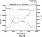
- FIG. 15is a graph showing a spectral transmittance through 1 cm of a waveguide for both TE 0 and TM 0 modes, and the difference in spectral transmittance.
- the present disclosuredescribes a substrate that is transparent at wavelengths of interest and upon which is deposited a waveguide core and cladding thin films.
- the refractive index of the coremay be greater than the refractive index of the cladding and/or the substrate. If the refractive index of the substrate is larger than that of the core, then the cladding may be several wavelengths thick to partially isolate the core from the substrate and reduce light leakage from the core waveguide mode into the substrate. If the refractive index of the substrate is less than that of the core, then there is no need for a cladding layer because the substrate itself acts as the cladding.
- a prism or a diffraction grating or a combination of the twomay be used to couple the light through the substrate into the waveguide.
- the prismmay be located on the outer surface of the substrate or on the window outside of the container.
- the gratingmay be located within the waveguide or adjacent the waveguide on the inside of the container. In some embodiments, the grating may be located at the waveguide-substrate interface.
- a prismfor example, as illustrated in FIG. 4 , may be configured to enable this wavevector matching. If the prism has a refractive index of n prism , and an angle of incidence of the light beam within the prism is ⁇ , then the necessary requirement for matching wavevector components is shown in Eq (1) or Eq (2) below:
- FIG. 5illustrates another embodiment of the present disclosure where the prism is replaced by a diffraction grating located within the core/cladding region of the waveguide.
- the gratingtakes the place of the prism.
- the angle of incidence which couples light into the waveguidemay be adjusted by adjusting a period of the grating, p.
- a depth of the gratingBy adjusting a depth of the grating, a coupling efficiency may be adjusted.
- the gratingcan be configured to efficiently couple light over a broader range of wavelengths and/or angles of incidence than for a traditional grating.
- the diffraction gratingadds or subtracts integer multiples of a grating vector from the component of the incident light wavevector in the plane of the waveguide, and when the sum of the two is equal to the waveguide mode wavevector, then light couples into the waveguide.
- the coupling equationis shown in Eq (6):
- coupling prisms from a variety of sourcesmay be used.
- Broadband light sourcesavailable from various sources, including Thorlabs, Newport Corp., and Edmund Scientific, may be used.
- Wafer substratesavailable from various sources, including University Wafer and WRS Materials, may be used.
- Thin film coatingsavailable from various sources, including Hionix, Inc., and Lionix BV, may be used.
- Spectrometersavailable from various sources, including Spectral Products, Newport, and Ocean Optics, may be used.
- Detectors available from various sources, including Thorlabs, Newport Inc., Cal Sensors, and Agiltronmay be used.
- FIG. 9illustrates an embodiment of the present disclosure, in which a ridge waveguide comprising multiple ridges is disposed on top of a substrate.
- the waveguidemay be configured such that the top surface of each ridge is slightly wider than the rest of the ridge as shown in FIG. 9 .
- the gaps at the top surface of the ridges between the ridgesare narrower than a size of particulates.
- the particulatesare primarily cardiomyocytes in a bioreactor solution with an elongated shape that is typically about 100 ⁇ m long and about 10 ⁇ m to 25 ⁇ m wide
- the gaps between ridges at the top surfacemay be only about 5 ⁇ m wide, thereby preventing entry of the cells into the region between the ridges where there is a stronger electric field but still allowing the fluid in the bioreactor to fill the spaces between the ridges and interact with the field from the waveguide mode.
- a ridge waveguideis provided and configured to enable waveguide spectroscopy of a fluid in contact with a core of the waveguide, while simultaneously excluding particulates of certain sizes from entering a high electric field region of the waveguide within the fluid.
- the waveguideis configured with multiple ridges spaced within substantially one wavelength or less such that a gap between ridges is less than a size of particulates within a surrounding fluid.
- the gap at the top surface of the ridges between the ridgesmay be smaller than a size of particulates, which is necessary to prevent particulate entry into the gaps.
- the ridge waveguidemay be configured with a top surface of at least one of the ridges being wider than a remainder portion of the at least one of ridges.
- the ridge waveguidemay comprise silicon on a silicon substrate.
- the materials of the ridge waveguidemay be selected from a group consisting of Si3N, Al2O3, Ta2O5, SixOyN1 ⁇ x ⁇ y, Si, Ge, diamond, ZnS, and ZnSe.
- a light from a light sourcemay be unpolarized, circularly polarized, or linearly polarized with a polarization orientation at 45°.
- the light sourcemay be linearly polarized such that an orientation of the light source is at 45° to the orientation for exciting either TE or TM waveguide modes
- a rotating polarizeras further illustrated in FIG. 11( a ) or 11 ( b ), is also provided.
- the lightis focused onto a waveguide having a waveguide core in contact with a sample and a waveguide cladding beneath the waveguide core.
- a substratemay be beneath the cladding.
- the rotating polarizeris shown to be positioned between the light source and the sample.
- Other configurations of the rotating polarizerare also contemplated.
- the rotating polarizermay be placed between the sample and the detector.
- FIG. 10further illustrates that a spectrometer or a monochromator may be positioned after the sample. It is to be understood that the spectrometer or the monochromator may also be placed between the light source and the sample. If the light source is a single wavelength light source (for example, a laser) or a tunable light source (for example, a tunable laser), then a spectrometer or monochromator may not be required.
- the rotating polarizermay rotate at a first specific frequency. This causes a polarization of a transmitted light to be modulated at a second specific frequency which may be a multiple of the rotation frequency. If the polarizer comprises segments as shown in FIG. 11( b ) , then the light transmitted through the polarizer should be alternately polarized in a direction of a TE waveguide mode and a TM waveguide mode, which are at 0° and 90°, respectively, in the embodiment illustrated. For a rotating sheet polarizer illustrated in FIG. 11( a ) , a polarization of a transmitted light varies continuously from 0° to 90° as the polarizer rotates.
- the rotating polarizerIf the rotating polarizer is placed in front of the waveguide, then the transmitted light focused onto the waveguide excites both the TE and TM modes with a 90° phase shift in their modulation intensity. If the rotating polarizer is placed after the waveguide then it transmits light from both TE and TM waveguide modes with a 90° phase shift between them.
- the light intensity for the transmitted TE and TM modesmay be separately measured and subtracted or divided to obtain a final spectrum.
- the intensity of the light for the combined transmitted TE and TM modesmay be measured by a single detector with a lock-in amplifier or a phase-sensitive synchronous detection electronics. If the light intensity transmitted through the waveguide for both modes is equal, then there is no change in the light intensity as the rotating polarizer rotates. The detected light intensity is modulated by the rotating polarizer only when there is a change in the transmitted light intensity of the two polarizations of the waveguide modes.
- the transmitted light intensity of the two polarizationsis different due to some factor other than absorption by the sample, such as different efficiencies of coupling light into the two modes, then the transmitted light intensity of the two modes can be compensated to be equal at the detector by adjusting the input polarization of the light source to put more light into the weaker mode, for example.
- a lock-in amplifiermay be used to synchronously detect the signal transmitted through the polarizer and waveguide. Because the two modes have a relative 90° phase shift in their modulation signals, the signal levels of the two modes can also be compensated and adjusted for zero output signal from the lock-in by adjusting the phase of the lock-in detection relative to the phase of the rotating polarizer.
- a polarizeris not rotating but is fixed at an orientation that passes light at 45° to that which excites either TE or TM waveguide modes.
- a polarizeris not rotating but fixed at a 45° orientation with respect to a waveguide. If an unpolarized light from a light source is transmitted through the polarizer, half of the light will excite a TE waveguide mode and half of the light will excite a TM waveguide mode.
- a polarizing beam splitteris provided, which reflects the light from one of these modes to one detector, while the transmitted light goes to a second detector.
- Two lock-in amplifiersmay be used to detect the TE and TM mode transmitted signals separately, as illustrated. If detected output signal amplitudes for the two modes are not equal, a gain of a detector electronics may be adjusted to make the detected output signal amplitudes form the two lock-in amplifiers equal.
- TE and TM modesinteract differently with the fluid in contact with the core of the waveguide.
- the electric field penetration into the fluiddepends on the type of mode and the specifics of the core/cladding thicknesses and refractive indices.
- an imaginary part of a waveguide mode indexwhich measures how quickly a light propagating in the waveguide gets attenuated, is plotted as a function of core thickness for a Si 3 N 4 core on a fused silica substrate and a glucose solution.
- the calculationmay be based on standard waveguide formulation that is known to one skilled in the art. In this calculation, the core and the cladding are not absorbing. Only the glucose solution is absorbing, so the imaginary part of the mode index is due to the absorption of light in the glucose solution.
- TE and TM modesmay exist in the waveguide. If the core is too thin, then no propagating modes of either polarization exist. As the core thickness increases from a starting point of zero, it first reaches a thickness for which the TE 0 mode can propagate as indicated by the value for the imaginary mode index for core thicknesses greater than about 320 nm. The large imaginary part of the mode index at this core thickness indicates that the TE 0 waveguide mode is highly attenuated. In general, this is desirable because it indicates that the mode is interacting strongly with the sample solution such as the glucose solution. As the core thickness is further increased, the attenuation of the TE 0 mode drops quickly.
- TM 0a first TM mode
- TM 0a first TM mode
- Italso has a very large imaginary mode index for the core thickness of about 540 nm, indicating that it is highly attenuated.
- the imaginary part of the mode index for the TE 0 mode at this core thicknessis much smaller. Therefore, at this core thickness the TM 0 mode is interacting much more strongly with the glucose solution than the TE 0 mode.
- the imaginary part of the mode index as a function of wavelengthis plotted in FIG. 14 for a fixed core thickness of 550 nm for both TE 0 and TM 0 modes.
- the nonzero value for the imaginary part of the mode indexis due entirely to the absorption by the glucose in the model calculation. It is clearly shown that a significant difference exists in the absorption due to the glucose between the two different modes, with the TM 0 mode exhibiting a larger attenuation than the TE 0 mode over the entire wavelength range.
- signals of transmittances of TE and TM modesmay be detected separately by different lock-in amplifiers. These signals may be digitally subtracted or divided by a controlling computer.
- FIG. 15exhibits calculated transmittance through a 10 mMol solution of glucose along a 1 cm waveguide for the TE 0 and TM 0 modes, as well as a transmittance difference spectrum. The transmittance difference spectrum clearly exhibits the absorption features of the glucose solution and may, therefore, be used to determine glucose concentration.
- Polarizer or polarizer segmentsmay be made from one or both of a sheet polarizer and a wire grid polarizer.
- Sheet polarizers and wire grid polarizersavailable from a number of sources for various wavelength ranges, including Thorlabs, Edmund Scientific, and Knight Optical. These may be cut to a proper shape and polarization angle and attached to a rotating “chopper” mount. Rotating “choppers” are available from various sources including Thorlabs, Edmund Scientific and Newport Corp.
- the polarizermay be a polarizing beamsplitter cube, a Glan-Thomson prism, a Wollaston prism, a Glan-Taylor prism, or any combination thereof.
Landscapes
- Physics & Mathematics (AREA)
- General Physics & Mathematics (AREA)
- Analytical Chemistry (AREA)
- Health & Medical Sciences (AREA)
- Life Sciences & Earth Sciences (AREA)
- Chemical & Material Sciences (AREA)
- Biochemistry (AREA)
- General Health & Medical Sciences (AREA)
- Immunology (AREA)
- Pathology (AREA)
- Spectroscopy & Molecular Physics (AREA)
- Optics & Photonics (AREA)
- Investigating Or Analysing Materials By Optical Means (AREA)
Abstract
Description
A mode index, nmode, for the waveguide mode may be calculated using equations known to one skilled in the art. Commercially available prisms that are transparent in the infrared region may be used. If a coupling prism angle is β, for example, as shown in
ξ=sin−1[npsin(θ−β)]+β. Eq (3)
The critical angle between the silicon substrate and water is determined by Eq (5):
where m is an integer and p is the period of the grating. In some embodiments, m=1 may be chosen.
Claims (23)
Priority Applications (1)
| Application Number | Priority Date | Filing Date | Title |
|---|---|---|---|
| US16/342,600US11249011B2 (en) | 2016-10-19 | 2017-10-19 | Apparatus and method for evanescent waveguide sensing |
Applications Claiming Priority (3)
| Application Number | Priority Date | Filing Date | Title |
|---|---|---|---|
| US201662409899P | 2016-10-19 | 2016-10-19 | |
| PCT/US2017/057345WO2018075744A2 (en) | 2016-10-19 | 2017-10-19 | Apparatus and method for evanescent waveguide sensing |
| US16/342,600US11249011B2 (en) | 2016-10-19 | 2017-10-19 | Apparatus and method for evanescent waveguide sensing |
Publications (2)
| Publication Number | Publication Date |
|---|---|
| US20190265157A1 US20190265157A1 (en) | 2019-08-29 |
| US11249011B2true US11249011B2 (en) | 2022-02-15 |
Family
ID=60245213
Family Applications (1)
| Application Number | Title | Priority Date | Filing Date |
|---|---|---|---|
| US16/342,600Active2038-08-17US11249011B2 (en) | 2016-10-19 | 2017-10-19 | Apparatus and method for evanescent waveguide sensing |
Country Status (5)
| Country | Link |
|---|---|
| US (1) | US11249011B2 (en) |
| EP (2) | EP4495578A3 (en) |
| JP (1) | JP7070984B2 (en) |
| CN (1) | CN109844496A (en) |
| WO (1) | WO2018075744A2 (en) |
Cited By (13)
| Publication number | Priority date | Publication date | Assignee | Title |
|---|---|---|---|---|
| US11749883B2 (en) | 2020-12-18 | 2023-09-05 | Aptiv Technologies Limited | Waveguide with radiation slots and parasitic elements for asymmetrical coverage |
| US11757166B2 (en) | 2020-11-10 | 2023-09-12 | Aptiv Technologies Limited | Surface-mount waveguide for vertical transitions of a printed circuit board |
| US11757165B2 (en) | 2020-12-22 | 2023-09-12 | Aptiv Technologies Limited | Folded waveguide for antenna |
| US11901601B2 (en) | 2020-12-18 | 2024-02-13 | Aptiv Technologies Limited | Waveguide with a zigzag for suppressing grating lobes |
| US11949145B2 (en) | 2021-08-03 | 2024-04-02 | Aptiv Technologies AG | Transition formed of LTCC material and having stubs that match input impedances between a single-ended port and differential ports |
| US11962087B2 (en) | 2021-03-22 | 2024-04-16 | Aptiv Technologies AG | Radar antenna system comprising an air waveguide antenna having a single layer material with air channels therein which is interfaced with a circuit board |
| US11962085B2 (en) | 2021-05-13 | 2024-04-16 | Aptiv Technologies AG | Two-part folded waveguide having a sinusoidal shape channel including horn shape radiating slots formed therein which are spaced apart by one-half wavelength |
| US12046818B2 (en) | 2021-04-30 | 2024-07-23 | Aptiv Technologies AG | Dielectric loaded waveguide for low loss signal distributions and small form factor antennas |
| US12058804B2 (en) | 2021-02-09 | 2024-08-06 | Aptiv Technologies AG | Formed waveguide antennas of a radar assembly |
| US12148992B2 (en) | 2023-01-25 | 2024-11-19 | Aptiv Technologies AG | Hybrid horn waveguide antenna |
| US12224502B2 (en) | 2021-10-14 | 2025-02-11 | Aptiv Technologies AG | Antenna-to-printed circuit board transition |
| US12265172B2 (en) | 2022-05-25 | 2025-04-01 | Aptiv Technologies AG | Vertical microstrip-to-waveguide transition |
| US12424767B2 (en) | 2022-11-15 | 2025-09-23 | Aptiv Technologies AG | Planar surface features for waveguide and antenna |
Families Citing this family (4)
| Publication number | Priority date | Publication date | Assignee | Title |
|---|---|---|---|---|
| JP7409881B2 (en)* | 2019-03-25 | 2024-01-09 | 旭化成エレクトロニクス株式会社 | Optical concentration measuring device and optical waveguide |
| JP7742699B2 (en)* | 2019-12-12 | 2025-09-22 | 旭化成エレクトロニクス株式会社 | Optical concentration measuring device and optical waveguide |
| JP7742700B2 (en)* | 2019-12-12 | 2025-09-22 | 旭化成エレクトロニクス株式会社 | Optical concentration measuring device and optical waveguide |
| CN115128735B (en)* | 2021-10-27 | 2024-05-07 | 赛丽科技(苏州)有限公司 | Optical sensor chip and optical sensing system |
Citations (14)
| Publication number | Priority date | Publication date | Assignee | Title |
|---|---|---|---|---|
| WO1991003728A1 (en) | 1989-09-01 | 1991-03-21 | Sira Limited | Guided optical wave chemical sensor systems |
| US5446534A (en) | 1993-03-05 | 1995-08-29 | Optical Solutions, Inc. | Broad band waveguide spectrometer |
| US5889279A (en) | 1996-08-02 | 1999-03-30 | Commissariat A L'energie Atomique | Tubular evanescent wave sensor for molecular absorption spectroscopy |
| US6268915B1 (en) | 1997-08-06 | 2001-07-31 | Michael Abraham | Micropolarimeter |
| US20020003627A1 (en) | 2000-03-13 | 2002-01-10 | Rieder Ronald J. | Doubly-differential interferometer and method for evanescent wave surface detection |
| JP2005300212A (en) | 2004-04-07 | 2005-10-27 | Nippon Telegr & Teleph Corp <Ntt> | Optical waveguide sensor and manufacturing method thereof |
| JP2007101471A (en) | 2005-10-07 | 2007-04-19 | National Institute Of Advanced Industrial & Technology | Slab optical waveguide spectral chemical sensor |
| JP2008064685A (en) | 2006-09-08 | 2008-03-21 | Dainippon Printing Co Ltd | Contamination evaluation method, contamination evaluation apparatus, and optical member manufacturing method |
| CH701504A2 (en) | 2009-07-27 | 2011-01-31 | Creoptix Gmbh | Integrated optical sensor with external liquid crystal modulator. |
| EP2450693A1 (en) | 2010-11-08 | 2012-05-09 | Nederlandse Organisatie voor toegepast -natuurwetenschappelijk onderzoek TNO | An arrayed waveguide grating (AWG) |
| US20160041160A1 (en) | 2014-08-05 | 2016-02-11 | Kabushiki Kaisha Toshiba | Specimen measurement apparatus and specimen measurement method |
| WO2016086090A1 (en) | 2014-11-26 | 2016-06-02 | Massachusetts Institute Of Technology | Methods and apparatus for pedestal ring resonators |
| JP2016114357A (en) | 2014-12-10 | 2016-06-23 | 学校法人日本大学 | Abo type blood back inspection device, and optical abo type blood back inspection method |
| US20160363728A1 (en)* | 2015-06-12 | 2016-12-15 | Pacific Biosciences Of California, Inc. | Integrated target waveguide devices and systems for optical coupling |
Family Cites Families (8)
| Publication number | Priority date | Publication date | Assignee | Title |
|---|---|---|---|---|
| JP2701740B2 (en)* | 1994-04-28 | 1998-01-21 | 株式会社島津製作所 | Total reflection absorption spectrum measurement device |
| JP3441056B2 (en)* | 1999-06-10 | 2003-08-25 | 日本電信電話株式会社 | Cell for infrared absorption measurement using silicon waveguide with concentrated film |
| JP4018603B2 (en)* | 2003-08-08 | 2007-12-05 | 日本電信電話株式会社 | Optical waveguide sensor |
| WO2010003808A2 (en)* | 2008-07-07 | 2010-01-14 | Kildal Antenna Consulting Ab | Waveguides and transmission lines in gaps between parallel conducting surfaces |
| FR2966916B1 (en)* | 2010-11-03 | 2012-11-16 | Thermor Pacific | METALLIC BODY FRAME ELEMENT FORMING CORNER |
| JP5503505B2 (en)* | 2010-11-15 | 2014-05-28 | 日東電工株式会社 | Colorimetric sensor cell, colorimetric sensor and method for producing colorimetric sensor cell |
| EP2862227A1 (en)* | 2012-06-18 | 2015-04-22 | Gapwaves AB | Gap waveguide structures for thz applications |
| CN103532014B (en)* | 2013-10-31 | 2015-08-26 | 中国科学院半导体研究所 | A kind of distribution bragg feedback tunable laser and preparation method thereof |
- 2017
- 2017-10-19CNCN201780064654.2Apatent/CN109844496A/enactivePending
- 2017-10-19WOPCT/US2017/057345patent/WO2018075744A2/ennot_activeCeased
- 2017-10-19JPJP2019520841Apatent/JP7070984B2/enactiveActive
- 2017-10-19EPEP24209926.5Apatent/EP4495578A3/enactivePending
- 2017-10-19EPEP17794154.9Apatent/EP3529590B1/enactiveActive
- 2017-10-19USUS16/342,600patent/US11249011B2/enactiveActive
Patent Citations (14)
| Publication number | Priority date | Publication date | Assignee | Title |
|---|---|---|---|---|
| WO1991003728A1 (en) | 1989-09-01 | 1991-03-21 | Sira Limited | Guided optical wave chemical sensor systems |
| US5446534A (en) | 1993-03-05 | 1995-08-29 | Optical Solutions, Inc. | Broad band waveguide spectrometer |
| US5889279A (en) | 1996-08-02 | 1999-03-30 | Commissariat A L'energie Atomique | Tubular evanescent wave sensor for molecular absorption spectroscopy |
| US6268915B1 (en) | 1997-08-06 | 2001-07-31 | Michael Abraham | Micropolarimeter |
| US20020003627A1 (en) | 2000-03-13 | 2002-01-10 | Rieder Ronald J. | Doubly-differential interferometer and method for evanescent wave surface detection |
| JP2005300212A (en) | 2004-04-07 | 2005-10-27 | Nippon Telegr & Teleph Corp <Ntt> | Optical waveguide sensor and manufacturing method thereof |
| JP2007101471A (en) | 2005-10-07 | 2007-04-19 | National Institute Of Advanced Industrial & Technology | Slab optical waveguide spectral chemical sensor |
| JP2008064685A (en) | 2006-09-08 | 2008-03-21 | Dainippon Printing Co Ltd | Contamination evaluation method, contamination evaluation apparatus, and optical member manufacturing method |
| CH701504A2 (en) | 2009-07-27 | 2011-01-31 | Creoptix Gmbh | Integrated optical sensor with external liquid crystal modulator. |
| EP2450693A1 (en) | 2010-11-08 | 2012-05-09 | Nederlandse Organisatie voor toegepast -natuurwetenschappelijk onderzoek TNO | An arrayed waveguide grating (AWG) |
| US20160041160A1 (en) | 2014-08-05 | 2016-02-11 | Kabushiki Kaisha Toshiba | Specimen measurement apparatus and specimen measurement method |
| WO2016086090A1 (en) | 2014-11-26 | 2016-06-02 | Massachusetts Institute Of Technology | Methods and apparatus for pedestal ring resonators |
| JP2016114357A (en) | 2014-12-10 | 2016-06-23 | 学校法人日本大学 | Abo type blood back inspection device, and optical abo type blood back inspection method |
| US20160363728A1 (en)* | 2015-06-12 | 2016-12-15 | Pacific Biosciences Of California, Inc. | Integrated target waveguide devices and systems for optical coupling |
Non-Patent Citations (6)
| Title |
|---|
| Barrios et al., "Demonstraction of Slot-Waveguide Structures on Silicon Nitride / Silicon Oxide Platform," Optics Express, 2007, 15(11):6846-6856. |
| European Office Action for EP Application No. 17794154.9 dated Apr. 30, 2020 (21 pages). |
| Japanese Office Action for JP Application No. 2019-520841 dated Aug. 2, 2021 (11 pages). |
| Khodadad et al., "Optimization of Multiple-Slot Waveguides for Biochemical Sensing," Applied Optics, 2014, 53(23):5169-5178. |
| Lukosz, "Integrated Optical Chemical and Direct Biochemical Sensors," Sensors and Actuators, 1995, 29:37-50. |
| PCT International Search Report and Written Opinion for PCT Application No. PCT/US2017/057345 dated May 3, 2018 (18 pages). |
Cited By (13)
| Publication number | Priority date | Publication date | Assignee | Title |
|---|---|---|---|---|
| US11757166B2 (en) | 2020-11-10 | 2023-09-12 | Aptiv Technologies Limited | Surface-mount waveguide for vertical transitions of a printed circuit board |
| US11901601B2 (en) | 2020-12-18 | 2024-02-13 | Aptiv Technologies Limited | Waveguide with a zigzag for suppressing grating lobes |
| US11749883B2 (en) | 2020-12-18 | 2023-09-05 | Aptiv Technologies Limited | Waveguide with radiation slots and parasitic elements for asymmetrical coverage |
| US11757165B2 (en) | 2020-12-22 | 2023-09-12 | Aptiv Technologies Limited | Folded waveguide for antenna |
| US12058804B2 (en) | 2021-02-09 | 2024-08-06 | Aptiv Technologies AG | Formed waveguide antennas of a radar assembly |
| US11962087B2 (en) | 2021-03-22 | 2024-04-16 | Aptiv Technologies AG | Radar antenna system comprising an air waveguide antenna having a single layer material with air channels therein which is interfaced with a circuit board |
| US12046818B2 (en) | 2021-04-30 | 2024-07-23 | Aptiv Technologies AG | Dielectric loaded waveguide for low loss signal distributions and small form factor antennas |
| US11962085B2 (en) | 2021-05-13 | 2024-04-16 | Aptiv Technologies AG | Two-part folded waveguide having a sinusoidal shape channel including horn shape radiating slots formed therein which are spaced apart by one-half wavelength |
| US11949145B2 (en) | 2021-08-03 | 2024-04-02 | Aptiv Technologies AG | Transition formed of LTCC material and having stubs that match input impedances between a single-ended port and differential ports |
| US12224502B2 (en) | 2021-10-14 | 2025-02-11 | Aptiv Technologies AG | Antenna-to-printed circuit board transition |
| US12265172B2 (en) | 2022-05-25 | 2025-04-01 | Aptiv Technologies AG | Vertical microstrip-to-waveguide transition |
| US12424767B2 (en) | 2022-11-15 | 2025-09-23 | Aptiv Technologies AG | Planar surface features for waveguide and antenna |
| US12148992B2 (en) | 2023-01-25 | 2024-11-19 | Aptiv Technologies AG | Hybrid horn waveguide antenna |
Also Published As
| Publication number | Publication date |
|---|---|
| WO2018075744A2 (en) | 2018-04-26 |
| JP2019534453A (en) | 2019-11-28 |
| JP7070984B2 (en) | 2022-05-18 |
| US20190265157A1 (en) | 2019-08-29 |
| EP3529590B1 (en) | 2024-12-04 |
| EP4495578A2 (en) | 2025-01-22 |
| EP4495578A3 (en) | 2025-03-05 |
| WO2018075744A3 (en) | 2018-05-31 |
| EP3529590A2 (en) | 2019-08-28 |
| CN109844496A (en) | 2019-06-04 |
Similar Documents
| Publication | Publication Date | Title |
|---|---|---|
| US11249011B2 (en) | Apparatus and method for evanescent waveguide sensing | |
| CN108027313B (en) | Resonant periodic structures and methods of using them as filters and sensors | |
| US9285534B2 (en) | Fiber-optic surface plasmon resonance sensor and sensing method using the same | |
| CN102230986B (en) | An optical phase device and its application method and system | |
| EP1005634B1 (en) | Near normal incidence optical assaying method having wavelength and angle sensitivity | |
| US8605282B2 (en) | Method and apparatus for high precision spectroscopy | |
| KR101359169B1 (en) | Total reflection attenuation optical probe and aqueous solution spectrometric device | |
| Fiedler et al. | Incoherent broad-band cavity-enhanced absorption spectroscopy of liquids | |
| US7817278B2 (en) | Surface plasmon resonance sensor apparatus having multiple dielectric layers | |
| US20150204723A1 (en) | Optical phase device, method and system | |
| US8941831B2 (en) | Intra-cavity ellipsometer system and method | |
| US6137576A (en) | Optical transducers based on liquid crystalline phases | |
| Canning et al. | Large dynamic range SPR measurements using a ZnSe prism | |
| US5502560A (en) | Analytical sensor using grating light reflection spectroscopy | |
| Ayupov et al. | Searching for the starting approximation when solving inverse problems in ellipsometry and spectrophotometry | |
| EP2669658B1 (en) | Surface plasmon sensor and refractive index measurement method | |
| US20130120750A1 (en) | Optical phase device, method and system | |
| US20140327909A1 (en) | Method for exciting a sub-wavelength inclusion structure | |
| KR20090006942A (en) | Biosensor measuring device | |
| US20220120680A1 (en) | Method and apparatus for determining optical properties of a sample material | |
| WO2006109408A1 (en) | Total-reflection attenuation optical probe and far-ultraviolet spectrophotometer | |
| CN109443704B (en) | Phase-enhanced optical intensity detection method and system | |
| RU2170913C1 (en) | Process of spectroscopy of transition layer of conducting surface | |
| Ciprian et al. | Spectral interferometry-based surface plasmon resonance sensing of liquid analyte refractive index change | |
| Choporova et al. | Polarimetry at Novosibirsk terahertz free electron laser facility |
Legal Events
| Date | Code | Title | Description |
|---|---|---|---|
| AS | Assignment | Owner name:GENERAL ELECTRIC COMPANY, NEW YORK Free format text:ASSIGNMENT OF ASSIGNORS INTEREST;ASSIGNOR:CHALLENER, WILLIAM ALBERT;REEL/FRAME:048908/0708 Effective date:20161019 | |
| FEPP | Fee payment procedure | Free format text:ENTITY STATUS SET TO UNDISCOUNTED (ORIGINAL EVENT CODE: BIG.); ENTITY STATUS OF PATENT OWNER: LARGE ENTITY | |
| AS | Assignment | Owner name:GENERAL ELECTRIC COMPANY, NEW YORK Free format text:CORRECTIVE ASSIGNMENT TO CORRECT THE ASSIGNEE'S ADDRESS PREVIOUSLY RECORDED AT REEL: 048908 FRAME: 0708. ASSIGNOR(S) HEREBY CONFIRMS THE ASSIGNMENT;ASSIGNOR:CHALLENER, WILLIAM ALBERT;REEL/FRAME:048946/0183 Effective date:20161019 | |
| STPP | Information on status: patent application and granting procedure in general | Free format text:DOCKETED NEW CASE - READY FOR EXAMINATION | |
| AS | Assignment | Owner name:GLOBAL LIFE SCIENCES SOLUTIONS USA LLC, MASSACHUSETTS Free format text:ASSIGNMENT OF ASSIGNORS INTEREST;ASSIGNOR:GENERAL ELECTRIC COMPANY;REEL/FRAME:053966/0133 Effective date:20200320 | |
| STPP | Information on status: patent application and granting procedure in general | Free format text:NON FINAL ACTION MAILED | |
| STPP | Information on status: patent application and granting procedure in general | Free format text:RESPONSE TO NON-FINAL OFFICE ACTION ENTERED AND FORWARDED TO EXAMINER | |
| STPP | Information on status: patent application and granting procedure in general | Free format text:NOTICE OF ALLOWANCE MAILED -- APPLICATION RECEIVED IN OFFICE OF PUBLICATIONS | |
| STPP | Information on status: patent application and granting procedure in general | Free format text:AWAITING TC RESP., ISSUE FEE NOT PAID | |
| STPP | Information on status: patent application and granting procedure in general | Free format text:NOTICE OF ALLOWANCE MAILED -- APPLICATION RECEIVED IN OFFICE OF PUBLICATIONS | |
| STPP | Information on status: patent application and granting procedure in general | Free format text:PUBLICATIONS -- ISSUE FEE PAYMENT VERIFIED | |
| STCF | Information on status: patent grant | Free format text:PATENTED CASE | |
| MAFP | Maintenance fee payment | Free format text:PAYMENT OF MAINTENANCE FEE, 4TH YEAR, LARGE ENTITY (ORIGINAL EVENT CODE: M1551); ENTITY STATUS OF PATENT OWNER: LARGE ENTITY Year of fee payment:4 |