US11247439B2 - Display unit - Google Patents
Display unitDownload PDFInfo
- Publication number
- US11247439B2 US11247439B2US15/580,942US201615580942AUS11247439B2US 11247439 B2US11247439 B2US 11247439B2US 201615580942 AUS201615580942 AUS 201615580942AUS 11247439 B2US11247439 B2US 11247439B2
- Authority
- US
- United States
- Prior art keywords
- insulating layer
- substrate
- wiring line
- display unit
- light
- Prior art date
- Legal status (The legal status is an assumption and is not a legal conclusion. Google has not performed a legal analysis and makes no representation as to the accuracy of the status listed.)
- Active, expires
Links
Images


Classifications
- B—PERFORMING OPERATIONS; TRANSPORTING
- B32—LAYERED PRODUCTS
- B32B—LAYERED PRODUCTS, i.e. PRODUCTS BUILT-UP OF STRATA OF FLAT OR NON-FLAT, e.g. CELLULAR OR HONEYCOMB, FORM
- B32B27/00—Layered products comprising a layer of synthetic resin
- B32B27/06—Layered products comprising a layer of synthetic resin as the main or only constituent of a layer, which is next to another layer of the same or of a different material
- B32B27/08—Layered products comprising a layer of synthetic resin as the main or only constituent of a layer, which is next to another layer of the same or of a different material of synthetic resin
- B—PERFORMING OPERATIONS; TRANSPORTING
- B32—LAYERED PRODUCTS
- B32B—LAYERED PRODUCTS, i.e. PRODUCTS BUILT-UP OF STRATA OF FLAT OR NON-FLAT, e.g. CELLULAR OR HONEYCOMB, FORM
- B32B15/00—Layered products comprising a layer of metal
- B32B15/04—Layered products comprising a layer of metal comprising metal as the main or only constituent of a layer, which is next to another layer of the same or of a different material
- B32B15/08—Layered products comprising a layer of metal comprising metal as the main or only constituent of a layer, which is next to another layer of the same or of a different material of synthetic resin
- B32B15/082—Layered products comprising a layer of metal comprising metal as the main or only constituent of a layer, which is next to another layer of the same or of a different material of synthetic resin comprising vinyl resins; comprising acrylic resins
- B—PERFORMING OPERATIONS; TRANSPORTING
- B32—LAYERED PRODUCTS
- B32B—LAYERED PRODUCTS, i.e. PRODUCTS BUILT-UP OF STRATA OF FLAT OR NON-FLAT, e.g. CELLULAR OR HONEYCOMB, FORM
- B32B15/00—Layered products comprising a layer of metal
- B32B15/04—Layered products comprising a layer of metal comprising metal as the main or only constituent of a layer, which is next to another layer of the same or of a different material
- B32B15/08—Layered products comprising a layer of metal comprising metal as the main or only constituent of a layer, which is next to another layer of the same or of a different material of synthetic resin
- B32B15/088—Layered products comprising a layer of metal comprising metal as the main or only constituent of a layer, which is next to another layer of the same or of a different material of synthetic resin comprising polyamides
- B—PERFORMING OPERATIONS; TRANSPORTING
- B32—LAYERED PRODUCTS
- B32B—LAYERED PRODUCTS, i.e. PRODUCTS BUILT-UP OF STRATA OF FLAT OR NON-FLAT, e.g. CELLULAR OR HONEYCOMB, FORM
- B32B15/00—Layered products comprising a layer of metal
- B32B15/04—Layered products comprising a layer of metal comprising metal as the main or only constituent of a layer, which is next to another layer of the same or of a different material
- B32B15/08—Layered products comprising a layer of metal comprising metal as the main or only constituent of a layer, which is next to another layer of the same or of a different material of synthetic resin
- B32B15/092—Layered products comprising a layer of metal comprising metal as the main or only constituent of a layer, which is next to another layer of the same or of a different material of synthetic resin comprising epoxy resins
- B—PERFORMING OPERATIONS; TRANSPORTING
- B32—LAYERED PRODUCTS
- B32B—LAYERED PRODUCTS, i.e. PRODUCTS BUILT-UP OF STRATA OF FLAT OR NON-FLAT, e.g. CELLULAR OR HONEYCOMB, FORM
- B32B15/00—Layered products comprising a layer of metal
- B32B15/04—Layered products comprising a layer of metal comprising metal as the main or only constituent of a layer, which is next to another layer of the same or of a different material
- B32B15/08—Layered products comprising a layer of metal comprising metal as the main or only constituent of a layer, which is next to another layer of the same or of a different material of synthetic resin
- B32B15/098—Layered products comprising a layer of metal comprising metal as the main or only constituent of a layer, which is next to another layer of the same or of a different material of synthetic resin comprising condensation resins of aldehydes, e.g. with phenols, ureas or melamines
- B—PERFORMING OPERATIONS; TRANSPORTING
- B32—LAYERED PRODUCTS
- B32B—LAYERED PRODUCTS, i.e. PRODUCTS BUILT-UP OF STRATA OF FLAT OR NON-FLAT, e.g. CELLULAR OR HONEYCOMB, FORM
- B32B15/00—Layered products comprising a layer of metal
- B32B15/18—Layered products comprising a layer of metal comprising iron or steel
- B—PERFORMING OPERATIONS; TRANSPORTING
- B32—LAYERED PRODUCTS
- B32B—LAYERED PRODUCTS, i.e. PRODUCTS BUILT-UP OF STRATA OF FLAT OR NON-FLAT, e.g. CELLULAR OR HONEYCOMB, FORM
- B32B15/00—Layered products comprising a layer of metal
- B32B15/20—Layered products comprising a layer of metal comprising aluminium or copper
- B—PERFORMING OPERATIONS; TRANSPORTING
- B32—LAYERED PRODUCTS
- B32B—LAYERED PRODUCTS, i.e. PRODUCTS BUILT-UP OF STRATA OF FLAT OR NON-FLAT, e.g. CELLULAR OR HONEYCOMB, FORM
- B32B17/00—Layered products essentially comprising sheet glass, or glass, slag, or like fibres
- B32B17/06—Layered products essentially comprising sheet glass, or glass, slag, or like fibres comprising glass as the main or only constituent of a layer, next to another layer of a specific material
- B—PERFORMING OPERATIONS; TRANSPORTING
- B32—LAYERED PRODUCTS
- B32B—LAYERED PRODUCTS, i.e. PRODUCTS BUILT-UP OF STRATA OF FLAT OR NON-FLAT, e.g. CELLULAR OR HONEYCOMB, FORM
- B32B27/00—Layered products comprising a layer of synthetic resin
- B32B27/06—Layered products comprising a layer of synthetic resin as the main or only constituent of a layer, which is next to another layer of the same or of a different material
- B32B27/10—Layered products comprising a layer of synthetic resin as the main or only constituent of a layer, which is next to another layer of the same or of a different material of paper or cardboard
- B—PERFORMING OPERATIONS; TRANSPORTING
- B32—LAYERED PRODUCTS
- B32B—LAYERED PRODUCTS, i.e. PRODUCTS BUILT-UP OF STRATA OF FLAT OR NON-FLAT, e.g. CELLULAR OR HONEYCOMB, FORM
- B32B27/00—Layered products comprising a layer of synthetic resin
- B32B27/28—Layered products comprising a layer of synthetic resin comprising synthetic resins not wholly covered by any one of the sub-groups B32B27/30 - B32B27/42
- B32B27/281—Layered products comprising a layer of synthetic resin comprising synthetic resins not wholly covered by any one of the sub-groups B32B27/30 - B32B27/42 comprising polyimides
- B—PERFORMING OPERATIONS; TRANSPORTING
- B32—LAYERED PRODUCTS
- B32B—LAYERED PRODUCTS, i.e. PRODUCTS BUILT-UP OF STRATA OF FLAT OR NON-FLAT, e.g. CELLULAR OR HONEYCOMB, FORM
- B32B27/00—Layered products comprising a layer of synthetic resin
- B32B27/28—Layered products comprising a layer of synthetic resin comprising synthetic resins not wholly covered by any one of the sub-groups B32B27/30 - B32B27/42
- B32B27/283—Layered products comprising a layer of synthetic resin comprising synthetic resins not wholly covered by any one of the sub-groups B32B27/30 - B32B27/42 comprising polysiloxanes
- B—PERFORMING OPERATIONS; TRANSPORTING
- B32—LAYERED PRODUCTS
- B32B—LAYERED PRODUCTS, i.e. PRODUCTS BUILT-UP OF STRATA OF FLAT OR NON-FLAT, e.g. CELLULAR OR HONEYCOMB, FORM
- B32B27/00—Layered products comprising a layer of synthetic resin
- B32B27/28—Layered products comprising a layer of synthetic resin comprising synthetic resins not wholly covered by any one of the sub-groups B32B27/30 - B32B27/42
- B32B27/285—Layered products comprising a layer of synthetic resin comprising synthetic resins not wholly covered by any one of the sub-groups B32B27/30 - B32B27/42 comprising polyethers
- B—PERFORMING OPERATIONS; TRANSPORTING
- B32—LAYERED PRODUCTS
- B32B—LAYERED PRODUCTS, i.e. PRODUCTS BUILT-UP OF STRATA OF FLAT OR NON-FLAT, e.g. CELLULAR OR HONEYCOMB, FORM
- B32B27/00—Layered products comprising a layer of synthetic resin
- B32B27/28—Layered products comprising a layer of synthetic resin comprising synthetic resins not wholly covered by any one of the sub-groups B32B27/30 - B32B27/42
- B32B27/286—Layered products comprising a layer of synthetic resin comprising synthetic resins not wholly covered by any one of the sub-groups B32B27/30 - B32B27/42 comprising polysulphones; polysulfides
- B—PERFORMING OPERATIONS; TRANSPORTING
- B32—LAYERED PRODUCTS
- B32B—LAYERED PRODUCTS, i.e. PRODUCTS BUILT-UP OF STRATA OF FLAT OR NON-FLAT, e.g. CELLULAR OR HONEYCOMB, FORM
- B32B27/00—Layered products comprising a layer of synthetic resin
- B32B27/28—Layered products comprising a layer of synthetic resin comprising synthetic resins not wholly covered by any one of the sub-groups B32B27/30 - B32B27/42
- B32B27/288—Layered products comprising a layer of synthetic resin comprising synthetic resins not wholly covered by any one of the sub-groups B32B27/30 - B32B27/42 comprising polyketones
- B—PERFORMING OPERATIONS; TRANSPORTING
- B32—LAYERED PRODUCTS
- B32B—LAYERED PRODUCTS, i.e. PRODUCTS BUILT-UP OF STRATA OF FLAT OR NON-FLAT, e.g. CELLULAR OR HONEYCOMB, FORM
- B32B27/00—Layered products comprising a layer of synthetic resin
- B32B27/30—Layered products comprising a layer of synthetic resin comprising vinyl (co)polymers; comprising acrylic (co)polymers
- B32B27/302—Layered products comprising a layer of synthetic resin comprising vinyl (co)polymers; comprising acrylic (co)polymers comprising aromatic vinyl (co)polymers, e.g. styrenic (co)polymers
- B—PERFORMING OPERATIONS; TRANSPORTING
- B32—LAYERED PRODUCTS
- B32B—LAYERED PRODUCTS, i.e. PRODUCTS BUILT-UP OF STRATA OF FLAT OR NON-FLAT, e.g. CELLULAR OR HONEYCOMB, FORM
- B32B27/00—Layered products comprising a layer of synthetic resin
- B32B27/30—Layered products comprising a layer of synthetic resin comprising vinyl (co)polymers; comprising acrylic (co)polymers
- B32B27/308—Layered products comprising a layer of synthetic resin comprising vinyl (co)polymers; comprising acrylic (co)polymers comprising acrylic (co)polymers
- B—PERFORMING OPERATIONS; TRANSPORTING
- B32—LAYERED PRODUCTS
- B32B—LAYERED PRODUCTS, i.e. PRODUCTS BUILT-UP OF STRATA OF FLAT OR NON-FLAT, e.g. CELLULAR OR HONEYCOMB, FORM
- B32B27/00—Layered products comprising a layer of synthetic resin
- B32B27/32—Layered products comprising a layer of synthetic resin comprising polyolefins
- B32B27/325—Layered products comprising a layer of synthetic resin comprising polyolefins comprising polycycloolefins
- B—PERFORMING OPERATIONS; TRANSPORTING
- B32—LAYERED PRODUCTS
- B32B—LAYERED PRODUCTS, i.e. PRODUCTS BUILT-UP OF STRATA OF FLAT OR NON-FLAT, e.g. CELLULAR OR HONEYCOMB, FORM
- B32B27/00—Layered products comprising a layer of synthetic resin
- B32B27/34—Layered products comprising a layer of synthetic resin comprising polyamides
- B—PERFORMING OPERATIONS; TRANSPORTING
- B32—LAYERED PRODUCTS
- B32B—LAYERED PRODUCTS, i.e. PRODUCTS BUILT-UP OF STRATA OF FLAT OR NON-FLAT, e.g. CELLULAR OR HONEYCOMB, FORM
- B32B27/00—Layered products comprising a layer of synthetic resin
- B32B27/36—Layered products comprising a layer of synthetic resin comprising polyesters
- B32B27/365—Layered products comprising a layer of synthetic resin comprising polyesters comprising polycarbonates
- B—PERFORMING OPERATIONS; TRANSPORTING
- B32—LAYERED PRODUCTS
- B32B—LAYERED PRODUCTS, i.e. PRODUCTS BUILT-UP OF STRATA OF FLAT OR NON-FLAT, e.g. CELLULAR OR HONEYCOMB, FORM
- B32B27/00—Layered products comprising a layer of synthetic resin
- B32B27/38—Layered products comprising a layer of synthetic resin comprising epoxy resins
- B—PERFORMING OPERATIONS; TRANSPORTING
- B32—LAYERED PRODUCTS
- B32B—LAYERED PRODUCTS, i.e. PRODUCTS BUILT-UP OF STRATA OF FLAT OR NON-FLAT, e.g. CELLULAR OR HONEYCOMB, FORM
- B32B27/00—Layered products comprising a layer of synthetic resin
- B32B27/42—Layered products comprising a layer of synthetic resin comprising condensation resins of aldehydes, e.g. with phenols, ureas or melamines
- B—PERFORMING OPERATIONS; TRANSPORTING
- B32—LAYERED PRODUCTS
- B32B—LAYERED PRODUCTS, i.e. PRODUCTS BUILT-UP OF STRATA OF FLAT OR NON-FLAT, e.g. CELLULAR OR HONEYCOMB, FORM
- B32B3/00—Layered products comprising a layer with external or internal discontinuities or unevennesses, or a layer of non-planar shape; Layered products comprising a layer having particular features of form
- B32B3/02—Layered products comprising a layer with external or internal discontinuities or unevennesses, or a layer of non-planar shape; Layered products comprising a layer having particular features of form characterised by features of form at particular places, e.g. in edge regions
- B32B3/08—Layered products comprising a layer with external or internal discontinuities or unevennesses, or a layer of non-planar shape; Layered products comprising a layer having particular features of form characterised by features of form at particular places, e.g. in edge regions characterised by added members at particular parts
- B—PERFORMING OPERATIONS; TRANSPORTING
- B32—LAYERED PRODUCTS
- B32B—LAYERED PRODUCTS, i.e. PRODUCTS BUILT-UP OF STRATA OF FLAT OR NON-FLAT, e.g. CELLULAR OR HONEYCOMB, FORM
- B32B7/00—Layered products characterised by the relation between layers; Layered products characterised by the relative orientation of features between layers, or by the relative values of a measurable parameter between layers, i.e. products comprising layers having different physical, chemical or physicochemical properties; Layered products characterised by the interconnection of layers
- B32B7/02—Physical, chemical or physicochemical properties
- B32B7/022—Mechanical properties
- B—PERFORMING OPERATIONS; TRANSPORTING
- B32—LAYERED PRODUCTS
- B32B—LAYERED PRODUCTS, i.e. PRODUCTS BUILT-UP OF STRATA OF FLAT OR NON-FLAT, e.g. CELLULAR OR HONEYCOMB, FORM
- B32B7/00—Layered products characterised by the relation between layers; Layered products characterised by the relative orientation of features between layers, or by the relative values of a measurable parameter between layers, i.e. products comprising layers having different physical, chemical or physicochemical properties; Layered products characterised by the interconnection of layers
- B32B7/04—Interconnection of layers
- B32B7/12—Interconnection of layers using interposed adhesives or interposed materials with bonding properties
- G—PHYSICS
- G09—EDUCATION; CRYPTOGRAPHY; DISPLAY; ADVERTISING; SEALS
- G09F—DISPLAYING; ADVERTISING; SIGNS; LABELS OR NAME-PLATES; SEALS
- G09F9/00—Indicating arrangements for variable information in which the information is built-up on a support by selection or combination of individual elements
- G09F9/30—Indicating arrangements for variable information in which the information is built-up on a support by selection or combination of individual elements in which the desired character or characters are formed by combining individual elements
- G09F9/302—Indicating arrangements for variable information in which the information is built-up on a support by selection or combination of individual elements in which the desired character or characters are formed by combining individual elements characterised by the form or geometrical disposition of the individual elements
- G—PHYSICS
- G09—EDUCATION; CRYPTOGRAPHY; DISPLAY; ADVERTISING; SEALS
- G09G—ARRANGEMENTS OR CIRCUITS FOR CONTROL OF INDICATING DEVICES USING STATIC MEANS TO PRESENT VARIABLE INFORMATION
- G09G3/00—Control arrangements or circuits, of interest only in connection with visual indicators other than cathode-ray tubes
- G09G3/20—Control arrangements or circuits, of interest only in connection with visual indicators other than cathode-ray tubes for presentation of an assembly of a number of characters, e.g. a page, by composing the assembly by combination of individual elements arranged in a matrix no fixed position being assigned to or needed to be assigned to the individual characters or partial characters
- G09G3/22—Control arrangements or circuits, of interest only in connection with visual indicators other than cathode-ray tubes for presentation of an assembly of a number of characters, e.g. a page, by composing the assembly by combination of individual elements arranged in a matrix no fixed position being assigned to or needed to be assigned to the individual characters or partial characters using controlled light sources
- G09G3/30—Control arrangements or circuits, of interest only in connection with visual indicators other than cathode-ray tubes for presentation of an assembly of a number of characters, e.g. a page, by composing the assembly by combination of individual elements arranged in a matrix no fixed position being assigned to or needed to be assigned to the individual characters or partial characters using controlled light sources using electroluminescent panels
- G09G3/32—Control arrangements or circuits, of interest only in connection with visual indicators other than cathode-ray tubes for presentation of an assembly of a number of characters, e.g. a page, by composing the assembly by combination of individual elements arranged in a matrix no fixed position being assigned to or needed to be assigned to the individual characters or partial characters using controlled light sources using electroluminescent panels semiconductive, e.g. using light-emitting diodes [LED]
- H—ELECTRICITY
- H01—ELECTRIC ELEMENTS
- H01L—SEMICONDUCTOR DEVICES NOT COVERED BY CLASS H10
- H01L23/00—Details of semiconductor or other solid state devices
- H01L23/28—Encapsulations, e.g. encapsulating layers, coatings, e.g. for protection
- H01L23/31—Encapsulations, e.g. encapsulating layers, coatings, e.g. for protection characterised by the arrangement or shape
- H01L23/3107—Encapsulations, e.g. encapsulating layers, coatings, e.g. for protection characterised by the arrangement or shape the device being completely enclosed
- H01L23/3114—Encapsulations, e.g. encapsulating layers, coatings, e.g. for protection characterised by the arrangement or shape the device being completely enclosed the device being a chip scale package, e.g. CSP
- H—ELECTRICITY
- H01—ELECTRIC ELEMENTS
- H01L—SEMICONDUCTOR DEVICES NOT COVERED BY CLASS H10
- H01L23/00—Details of semiconductor or other solid state devices
- H01L23/28—Encapsulations, e.g. encapsulating layers, coatings, e.g. for protection
- H01L23/31—Encapsulations, e.g. encapsulating layers, coatings, e.g. for protection characterised by the arrangement or shape
- H01L23/3107—Encapsulations, e.g. encapsulating layers, coatings, e.g. for protection characterised by the arrangement or shape the device being completely enclosed
- H01L23/3121—Encapsulations, e.g. encapsulating layers, coatings, e.g. for protection characterised by the arrangement or shape the device being completely enclosed a substrate forming part of the encapsulation
- H—ELECTRICITY
- H01—ELECTRIC ELEMENTS
- H01L—SEMICONDUCTOR DEVICES NOT COVERED BY CLASS H10
- H01L23/00—Details of semiconductor or other solid state devices
- H01L23/28—Encapsulations, e.g. encapsulating layers, coatings, e.g. for protection
- H01L23/31—Encapsulations, e.g. encapsulating layers, coatings, e.g. for protection characterised by the arrangement or shape
- H01L23/3107—Encapsulations, e.g. encapsulating layers, coatings, e.g. for protection characterised by the arrangement or shape the device being completely enclosed
- H01L23/3135—Double encapsulation or coating and encapsulation
- H—ELECTRICITY
- H01—ELECTRIC ELEMENTS
- H01L—SEMICONDUCTOR DEVICES NOT COVERED BY CLASS H10
- H01L23/00—Details of semiconductor or other solid state devices
- H01L23/28—Encapsulations, e.g. encapsulating layers, coatings, e.g. for protection
- H01L23/31—Encapsulations, e.g. encapsulating layers, coatings, e.g. for protection characterised by the arrangement or shape
- H01L23/3157—Partial encapsulation or coating
- H01L23/3192—Multilayer coating
- H—ELECTRICITY
- H01—ELECTRIC ELEMENTS
- H01L—SEMICONDUCTOR DEVICES NOT COVERED BY CLASS H10
- H01L23/00—Details of semiconductor or other solid state devices
- H01L23/48—Arrangements for conducting electric current to or from the solid state body in operation, e.g. leads, terminal arrangements ; Selection of materials therefor
- H01L23/488—Arrangements for conducting electric current to or from the solid state body in operation, e.g. leads, terminal arrangements ; Selection of materials therefor consisting of soldered or bonded constructions
- H01L23/498—Leads, i.e. metallisations or lead-frames on insulating substrates, e.g. chip carriers
- H01L23/49811—Additional leads joined to the metallisation on the insulating substrate, e.g. pins, bumps, wires, flat leads
- H—ELECTRICITY
- H01—ELECTRIC ELEMENTS
- H01L—SEMICONDUCTOR DEVICES NOT COVERED BY CLASS H10
- H01L23/00—Details of semiconductor or other solid state devices
- H01L23/48—Arrangements for conducting electric current to or from the solid state body in operation, e.g. leads, terminal arrangements ; Selection of materials therefor
- H01L23/488—Arrangements for conducting electric current to or from the solid state body in operation, e.g. leads, terminal arrangements ; Selection of materials therefor consisting of soldered or bonded constructions
- H01L23/498—Leads, i.e. metallisations or lead-frames on insulating substrates, e.g. chip carriers
- H01L23/49833—Leads, i.e. metallisations or lead-frames on insulating substrates, e.g. chip carriers the chip support structure consisting of a plurality of insulating substrates
- H—ELECTRICITY
- H01—ELECTRIC ELEMENTS
- H01L—SEMICONDUCTOR DEVICES NOT COVERED BY CLASS H10
- H01L23/00—Details of semiconductor or other solid state devices
- H01L23/52—Arrangements for conducting electric current within the device in operation from one component to another, i.e. interconnections, e.g. wires, lead frames
- H01L23/538—Arrangements for conducting electric current within the device in operation from one component to another, i.e. interconnections, e.g. wires, lead frames the interconnection structure between a plurality of semiconductor chips being formed on, or in, insulating substrates
- H01L23/5384—Conductive vias through the substrate with or without pins, e.g. buried coaxial conductors
- H—ELECTRICITY
- H01—ELECTRIC ELEMENTS
- H01L—SEMICONDUCTOR DEVICES NOT COVERED BY CLASS H10
- H01L23/00—Details of semiconductor or other solid state devices
- H01L23/52—Arrangements for conducting electric current within the device in operation from one component to another, i.e. interconnections, e.g. wires, lead frames
- H01L23/538—Arrangements for conducting electric current within the device in operation from one component to another, i.e. interconnections, e.g. wires, lead frames the interconnection structure between a plurality of semiconductor chips being formed on, or in, insulating substrates
- H01L23/5385—Assembly of a plurality of insulating substrates
- H—ELECTRICITY
- H01—ELECTRIC ELEMENTS
- H01L—SEMICONDUCTOR DEVICES NOT COVERED BY CLASS H10
- H01L25/00—Assemblies consisting of a plurality of semiconductor or other solid state devices
- H01L25/03—Assemblies consisting of a plurality of semiconductor or other solid state devices all the devices being of a type provided for in a single subclass of subclasses H10B, H10D, H10F, H10H, H10K or H10N, e.g. assemblies of rectifier diodes
- H01L25/04—Assemblies consisting of a plurality of semiconductor or other solid state devices all the devices being of a type provided for in a single subclass of subclasses H10B, H10D, H10F, H10H, H10K or H10N, e.g. assemblies of rectifier diodes the devices not having separate containers
- H01L25/075—Assemblies consisting of a plurality of semiconductor or other solid state devices all the devices being of a type provided for in a single subclass of subclasses H10B, H10D, H10F, H10H, H10K or H10N, e.g. assemblies of rectifier diodes the devices not having separate containers the devices being of a type provided for in group H10H20/00
- H01L25/0753—Assemblies consisting of a plurality of semiconductor or other solid state devices all the devices being of a type provided for in a single subclass of subclasses H10B, H10D, H10F, H10H, H10K or H10N, e.g. assemblies of rectifier diodes the devices not having separate containers the devices being of a type provided for in group H10H20/00 the devices being arranged next to each other
- H—ELECTRICITY
- H01—ELECTRIC ELEMENTS
- H01L—SEMICONDUCTOR DEVICES NOT COVERED BY CLASS H10
- H01L25/00—Assemblies consisting of a plurality of semiconductor or other solid state devices
- H01L25/16—Assemblies consisting of a plurality of semiconductor or other solid state devices the devices being of types provided for in two or more different subclasses of H10B, H10D, H10F, H10H, H10K or H10N, e.g. forming hybrid circuits
- H01L25/167—Assemblies consisting of a plurality of semiconductor or other solid state devices the devices being of types provided for in two or more different subclasses of H10B, H10D, H10F, H10H, H10K or H10N, e.g. forming hybrid circuits comprising optoelectronic devices, e.g. LED, photodiodes
- H01L33/30—
- H01L33/32—
- H01L33/54—
- H01L33/56—
- H01L33/62—
- H—ELECTRICITY
- H10—SEMICONDUCTOR DEVICES; ELECTRIC SOLID-STATE DEVICES NOT OTHERWISE PROVIDED FOR
- H10H—INORGANIC LIGHT-EMITTING SEMICONDUCTOR DEVICES HAVING POTENTIAL BARRIERS
- H10H20/00—Individual inorganic light-emitting semiconductor devices having potential barriers, e.g. light-emitting diodes [LED]
- H10H20/80—Constructional details
- H10H20/81—Bodies
- H10H20/822—Materials of the light-emitting regions
- H10H20/824—Materials of the light-emitting regions comprising only Group III-V materials, e.g. GaP
- H10H20/825—Materials of the light-emitting regions comprising only Group III-V materials, e.g. GaP containing nitrogen, e.g. GaN
- H—ELECTRICITY
- H10—SEMICONDUCTOR DEVICES; ELECTRIC SOLID-STATE DEVICES NOT OTHERWISE PROVIDED FOR
- H10H—INORGANIC LIGHT-EMITTING SEMICONDUCTOR DEVICES HAVING POTENTIAL BARRIERS
- H10H20/00—Individual inorganic light-emitting semiconductor devices having potential barriers, e.g. light-emitting diodes [LED]
- H10H20/80—Constructional details
- H10H20/85—Packages
- H10H20/852—Encapsulations
- H10H20/853—Encapsulations characterised by their shape
- H—ELECTRICITY
- H10—SEMICONDUCTOR DEVICES; ELECTRIC SOLID-STATE DEVICES NOT OTHERWISE PROVIDED FOR
- H10H—INORGANIC LIGHT-EMITTING SEMICONDUCTOR DEVICES HAVING POTENTIAL BARRIERS
- H10H20/00—Individual inorganic light-emitting semiconductor devices having potential barriers, e.g. light-emitting diodes [LED]
- H10H20/80—Constructional details
- H10H20/85—Packages
- H10H20/852—Encapsulations
- H10H20/854—Encapsulations characterised by their material, e.g. epoxy or silicone resins
- H—ELECTRICITY
- H10—SEMICONDUCTOR DEVICES; ELECTRIC SOLID-STATE DEVICES NOT OTHERWISE PROVIDED FOR
- H10H—INORGANIC LIGHT-EMITTING SEMICONDUCTOR DEVICES HAVING POTENTIAL BARRIERS
- H10H20/00—Individual inorganic light-emitting semiconductor devices having potential barriers, e.g. light-emitting diodes [LED]
- H10H20/80—Constructional details
- H10H20/85—Packages
- H10H20/857—Interconnections, e.g. lead-frames, bond wires or solder balls
- B—PERFORMING OPERATIONS; TRANSPORTING
- B32—LAYERED PRODUCTS
- B32B—LAYERED PRODUCTS, i.e. PRODUCTS BUILT-UP OF STRATA OF FLAT OR NON-FLAT, e.g. CELLULAR OR HONEYCOMB, FORM
- B32B2250/00—Layers arrangement
- B32B2250/02—2 layers
- B—PERFORMING OPERATIONS; TRANSPORTING
- B32—LAYERED PRODUCTS
- B32B—LAYERED PRODUCTS, i.e. PRODUCTS BUILT-UP OF STRATA OF FLAT OR NON-FLAT, e.g. CELLULAR OR HONEYCOMB, FORM
- B32B2250/00—Layers arrangement
- B32B2250/03—3 layers
- B—PERFORMING OPERATIONS; TRANSPORTING
- B32—LAYERED PRODUCTS
- B32B—LAYERED PRODUCTS, i.e. PRODUCTS BUILT-UP OF STRATA OF FLAT OR NON-FLAT, e.g. CELLULAR OR HONEYCOMB, FORM
- B32B2250/00—Layers arrangement
- B32B2250/24—All layers being polymeric
- B—PERFORMING OPERATIONS; TRANSPORTING
- B32—LAYERED PRODUCTS
- B32B—LAYERED PRODUCTS, i.e. PRODUCTS BUILT-UP OF STRATA OF FLAT OR NON-FLAT, e.g. CELLULAR OR HONEYCOMB, FORM
- B32B2255/00—Coating on the layer surface
- B32B2255/20—Inorganic coating
- B—PERFORMING OPERATIONS; TRANSPORTING
- B32—LAYERED PRODUCTS
- B32B—LAYERED PRODUCTS, i.e. PRODUCTS BUILT-UP OF STRATA OF FLAT OR NON-FLAT, e.g. CELLULAR OR HONEYCOMB, FORM
- B32B2255/00—Coating on the layer surface
- B32B2255/20—Inorganic coating
- B32B2255/205—Metallic coating
- B—PERFORMING OPERATIONS; TRANSPORTING
- B32—LAYERED PRODUCTS
- B32B—LAYERED PRODUCTS, i.e. PRODUCTS BUILT-UP OF STRATA OF FLAT OR NON-FLAT, e.g. CELLULAR OR HONEYCOMB, FORM
- B32B2255/00—Coating on the layer surface
- B32B2255/28—Multiple coating on one surface
- B—PERFORMING OPERATIONS; TRANSPORTING
- B32—LAYERED PRODUCTS
- B32B—LAYERED PRODUCTS, i.e. PRODUCTS BUILT-UP OF STRATA OF FLAT OR NON-FLAT, e.g. CELLULAR OR HONEYCOMB, FORM
- B32B2307/00—Properties of the layers or laminate
- B32B2307/70—Other properties
- B32B2307/71—Resistive to light or to UV
- B—PERFORMING OPERATIONS; TRANSPORTING
- B32—LAYERED PRODUCTS
- B32B—LAYERED PRODUCTS, i.e. PRODUCTS BUILT-UP OF STRATA OF FLAT OR NON-FLAT, e.g. CELLULAR OR HONEYCOMB, FORM
- B32B2307/00—Properties of the layers or laminate
- B32B2307/70—Other properties
- B32B2307/724—Permeability to gases, adsorption
- B32B2307/7242—Non-permeable
- B32B2307/7246—Water vapor barrier
- B—PERFORMING OPERATIONS; TRANSPORTING
- B32—LAYERED PRODUCTS
- B32B—LAYERED PRODUCTS, i.e. PRODUCTS BUILT-UP OF STRATA OF FLAT OR NON-FLAT, e.g. CELLULAR OR HONEYCOMB, FORM
- B32B2307/00—Properties of the layers or laminate
- B32B2307/70—Other properties
- B32B2307/732—Dimensional properties
- B—PERFORMING OPERATIONS; TRANSPORTING
- B32—LAYERED PRODUCTS
- B32B—LAYERED PRODUCTS, i.e. PRODUCTS BUILT-UP OF STRATA OF FLAT OR NON-FLAT, e.g. CELLULAR OR HONEYCOMB, FORM
- B32B2307/00—Properties of the layers or laminate
- B32B2307/70—Other properties
- B32B2307/74—Oxygen absorber
- B—PERFORMING OPERATIONS; TRANSPORTING
- B32—LAYERED PRODUCTS
- B32B—LAYERED PRODUCTS, i.e. PRODUCTS BUILT-UP OF STRATA OF FLAT OR NON-FLAT, e.g. CELLULAR OR HONEYCOMB, FORM
- B32B2457/00—Electrical equipment
- B32B2457/20—Displays, e.g. liquid crystal displays, plasma displays
- B32B2457/202—LCD, i.e. liquid crystal displays
- B—PERFORMING OPERATIONS; TRANSPORTING
- B32—LAYERED PRODUCTS
- B32B—LAYERED PRODUCTS, i.e. PRODUCTS BUILT-UP OF STRATA OF FLAT OR NON-FLAT, e.g. CELLULAR OR HONEYCOMB, FORM
- B32B27/00—Layered products comprising a layer of synthetic resin
- G—PHYSICS
- G09—EDUCATION; CRYPTOGRAPHY; DISPLAY; ADVERTISING; SEALS
- G09F—DISPLAYING; ADVERTISING; SIGNS; LABELS OR NAME-PLATES; SEALS
- G09F9/00—Indicating arrangements for variable information in which the information is built-up on a support by selection or combination of individual elements
- G—PHYSICS
- G09—EDUCATION; CRYPTOGRAPHY; DISPLAY; ADVERTISING; SEALS
- G09F—DISPLAYING; ADVERTISING; SIGNS; LABELS OR NAME-PLATES; SEALS
- G09F9/00—Indicating arrangements for variable information in which the information is built-up on a support by selection or combination of individual elements
- G09F9/30—Indicating arrangements for variable information in which the information is built-up on a support by selection or combination of individual elements in which the desired character or characters are formed by combining individual elements
- G09F9/33—Indicating arrangements for variable information in which the information is built-up on a support by selection or combination of individual elements in which the desired character or characters are formed by combining individual elements being semiconductor devices, e.g. diodes
- G—PHYSICS
- G09—EDUCATION; CRYPTOGRAPHY; DISPLAY; ADVERTISING; SEALS
- G09G—ARRANGEMENTS OR CIRCUITS FOR CONTROL OF INDICATING DEVICES USING STATIC MEANS TO PRESENT VARIABLE INFORMATION
- G09G2300/00—Aspects of the constitution of display devices
- G09G2300/04—Structural and physical details of display devices
- G09G2300/0404—Matrix technologies
- G09G2300/0408—Integration of the drivers onto the display substrate
- G—PHYSICS
- G09—EDUCATION; CRYPTOGRAPHY; DISPLAY; ADVERTISING; SEALS
- G09G—ARRANGEMENTS OR CIRCUITS FOR CONTROL OF INDICATING DEVICES USING STATIC MEANS TO PRESENT VARIABLE INFORMATION
- G09G2310/00—Command of the display device
- G09G2310/02—Addressing, scanning or driving the display screen or processing steps related thereto
- G09G2310/0202—Addressing of scan or signal lines
- G09G2310/0221—Addressing of scan or signal lines with use of split matrices
- G—PHYSICS
- G09—EDUCATION; CRYPTOGRAPHY; DISPLAY; ADVERTISING; SEALS
- G09G—ARRANGEMENTS OR CIRCUITS FOR CONTROL OF INDICATING DEVICES USING STATIC MEANS TO PRESENT VARIABLE INFORMATION
- G09G2320/00—Control of display operating conditions
- G09G2320/06—Adjustment of display parameters
- G09G2320/0613—The adjustment depending on the type of the information to be displayed
- G09G2320/062—Adjustment of illumination source parameters
- G—PHYSICS
- G09—EDUCATION; CRYPTOGRAPHY; DISPLAY; ADVERTISING; SEALS
- G09G—ARRANGEMENTS OR CIRCUITS FOR CONTROL OF INDICATING DEVICES USING STATIC MEANS TO PRESENT VARIABLE INFORMATION
- G09G2320/00—Control of display operating conditions
- G09G2320/06—Adjustment of display parameters
- G09G2320/0626—Adjustment of display parameters for control of overall brightness
- G09G2320/064—Adjustment of display parameters for control of overall brightness by time modulation of the brightness of the illumination source
- G—PHYSICS
- G09—EDUCATION; CRYPTOGRAPHY; DISPLAY; ADVERTISING; SEALS
- G09G—ARRANGEMENTS OR CIRCUITS FOR CONTROL OF INDICATING DEVICES USING STATIC MEANS TO PRESENT VARIABLE INFORMATION
- G09G2320/00—Control of display operating conditions
- G09G2320/06—Adjustment of display parameters
- G09G2320/0673—Adjustment of display parameters for control of gamma adjustment, e.g. selecting another gamma curve
- G—PHYSICS
- G09—EDUCATION; CRYPTOGRAPHY; DISPLAY; ADVERTISING; SEALS
- G09G—ARRANGEMENTS OR CIRCUITS FOR CONTROL OF INDICATING DEVICES USING STATIC MEANS TO PRESENT VARIABLE INFORMATION
- G09G2360/00—Aspects of the architecture of display systems
- G09G2360/04—Display device controller operating with a plurality of display units
- G—PHYSICS
- G09—EDUCATION; CRYPTOGRAPHY; DISPLAY; ADVERTISING; SEALS
- G09G—ARRANGEMENTS OR CIRCUITS FOR CONTROL OF INDICATING DEVICES USING STATIC MEANS TO PRESENT VARIABLE INFORMATION
- G09G2360/00—Aspects of the architecture of display systems
- G09G2360/12—Frame memory handling
- G09G2360/122—Tiling
- G—PHYSICS
- G09—EDUCATION; CRYPTOGRAPHY; DISPLAY; ADVERTISING; SEALS
- G09G—ARRANGEMENTS OR CIRCUITS FOR CONTROL OF INDICATING DEVICES USING STATIC MEANS TO PRESENT VARIABLE INFORMATION
- G09G3/00—Control arrangements or circuits, of interest only in connection with visual indicators other than cathode-ray tubes
- G09G3/20—Control arrangements or circuits, of interest only in connection with visual indicators other than cathode-ray tubes for presentation of an assembly of a number of characters, e.g. a page, by composing the assembly by combination of individual elements arranged in a matrix no fixed position being assigned to or needed to be assigned to the individual characters or partial characters
- G09G3/22—Control arrangements or circuits, of interest only in connection with visual indicators other than cathode-ray tubes for presentation of an assembly of a number of characters, e.g. a page, by composing the assembly by combination of individual elements arranged in a matrix no fixed position being assigned to or needed to be assigned to the individual characters or partial characters using controlled light sources
- G09G3/30—Control arrangements or circuits, of interest only in connection with visual indicators other than cathode-ray tubes for presentation of an assembly of a number of characters, e.g. a page, by composing the assembly by combination of individual elements arranged in a matrix no fixed position being assigned to or needed to be assigned to the individual characters or partial characters using controlled light sources using electroluminescent panels
- G09G3/32—Control arrangements or circuits, of interest only in connection with visual indicators other than cathode-ray tubes for presentation of an assembly of a number of characters, e.g. a page, by composing the assembly by combination of individual elements arranged in a matrix no fixed position being assigned to or needed to be assigned to the individual characters or partial characters using controlled light sources using electroluminescent panels semiconductive, e.g. using light-emitting diodes [LED]
- G09G3/3208—Control arrangements or circuits, of interest only in connection with visual indicators other than cathode-ray tubes for presentation of an assembly of a number of characters, e.g. a page, by composing the assembly by combination of individual elements arranged in a matrix no fixed position being assigned to or needed to be assigned to the individual characters or partial characters using controlled light sources using electroluminescent panels semiconductive, e.g. using light-emitting diodes [LED] organic, e.g. using organic light-emitting diodes [OLED]
- G09G3/3225—Control arrangements or circuits, of interest only in connection with visual indicators other than cathode-ray tubes for presentation of an assembly of a number of characters, e.g. a page, by composing the assembly by combination of individual elements arranged in a matrix no fixed position being assigned to or needed to be assigned to the individual characters or partial characters using controlled light sources using electroluminescent panels semiconductive, e.g. using light-emitting diodes [LED] organic, e.g. using organic light-emitting diodes [OLED] using an active matrix
- H—ELECTRICITY
- H01—ELECTRIC ELEMENTS
- H01L—SEMICONDUCTOR DEVICES NOT COVERED BY CLASS H10
- H01L23/00—Details of semiconductor or other solid state devices
- H01L23/12—Mountings, e.g. non-detachable insulating substrates
- H01L23/14—Mountings, e.g. non-detachable insulating substrates characterised by the material or its electrical properties
- H01L23/142—Metallic substrates having insulating layers
- H—ELECTRICITY
- H01—ELECTRIC ELEMENTS
- H01L—SEMICONDUCTOR DEVICES NOT COVERED BY CLASS H10
- H01L23/00—Details of semiconductor or other solid state devices
- H01L23/48—Arrangements for conducting electric current to or from the solid state body in operation, e.g. leads, terminal arrangements ; Selection of materials therefor
- H01L23/488—Arrangements for conducting electric current to or from the solid state body in operation, e.g. leads, terminal arrangements ; Selection of materials therefor consisting of soldered or bonded constructions
- H01L23/498—Leads, i.e. metallisations or lead-frames on insulating substrates, e.g. chip carriers
- H01L23/49822—Multilayer substrates
- H—ELECTRICITY
- H01—ELECTRIC ELEMENTS
- H01L—SEMICONDUCTOR DEVICES NOT COVERED BY CLASS H10
- H01L23/00—Details of semiconductor or other solid state devices
- H01L23/48—Arrangements for conducting electric current to or from the solid state body in operation, e.g. leads, terminal arrangements ; Selection of materials therefor
- H01L23/488—Arrangements for conducting electric current to or from the solid state body in operation, e.g. leads, terminal arrangements ; Selection of materials therefor consisting of soldered or bonded constructions
- H01L23/498—Leads, i.e. metallisations or lead-frames on insulating substrates, e.g. chip carriers
- H01L23/49827—Via connections through the substrates, e.g. pins going through the substrate, coaxial cables
- H—ELECTRICITY
- H01—ELECTRIC ELEMENTS
- H01L—SEMICONDUCTOR DEVICES NOT COVERED BY CLASS H10
- H01L23/00—Details of semiconductor or other solid state devices
- H01L23/52—Arrangements for conducting electric current within the device in operation from one component to another, i.e. interconnections, e.g. wires, lead frames
- H01L23/538—Arrangements for conducting electric current within the device in operation from one component to another, i.e. interconnections, e.g. wires, lead frames the interconnection structure between a plurality of semiconductor chips being formed on, or in, insulating substrates
- H01L23/5383—Multilayer substrates
- H—ELECTRICITY
- H01—ELECTRIC ELEMENTS
- H01L—SEMICONDUCTOR DEVICES NOT COVERED BY CLASS H10
- H01L23/00—Details of semiconductor or other solid state devices
- H01L23/52—Arrangements for conducting electric current within the device in operation from one component to another, i.e. interconnections, e.g. wires, lead frames
- H01L23/538—Arrangements for conducting electric current within the device in operation from one component to another, i.e. interconnections, e.g. wires, lead frames the interconnection structure between a plurality of semiconductor chips being formed on, or in, insulating substrates
- H01L23/5386—Geometry or layout of the interconnection structure
Definitions
- the technologyrelates to a display unit including, for example, a light-emitting diode (LED) as a light-emission device.
- a display unitincluding, for example, a light-emitting diode (LED) as a light-emission device.
- LEDlight-emitting diode
- Conceivable methods of suppressing occurrence of ionic migrationinclude increasing a wiring interval, lowering a voltage between wiring lines, using a resin material having a small amount of remaining ions that couple to a wiring line (e.g., a copper (Cu) wiring line), and providing a member that suppresses entering of moisture from outside.
- a wiring linee.g., a copper (Cu) wiring line
- the wiring interval, application of the voltage, and the resin materialare determined by other factors in designing a device and thus, it is difficult to make a modification thereto.
- a method of providing a member that suppresses entering of moisture from outsideis used. Specifically, entering of moisture is suppressed by forming an inorganic barrier layer on an insulating layer by vapor deposition, or by attaching a film, on which an inorganic barrier layer is formed, to a substrate.
- PTL 1discloses an image display unit that uses a so-called multilayered wiring board, in which a footprint of an electronic component is increased, while an increase in density of wiring lines is reduced, by forming a wiring pattern inside a substrate.
- a printed circuit boardis configured of a base material having an insulation property and an organic resin material such as an epoxy resin.
- an inorganic barrier layeris provided on a substrate (an organic substrate) including such an organic resin material, entering of moisture from the inorganic barrier layer surface is suppressed.
- a voidoccurs due to peeling off of an interface between the organic substrate, which has weak adhesion due to moisture contained in the organic substrate and gas generated from the organic resin material, and the inorganic barrier layer.
- a display unitincludes: a substrate; a wiring line and a light-emission section that are provided on the substrate; an insulating layer covering the wiring line and the light-emission section, and provided on an entire surface of the substrate; and a sealing layer provided on an entire surface of the insulating layer, and including a resin material having an oxygen transmission rate higher than a water-vapor transmission rate.
- the sealing layer that includes the resin material having the oxygen transmission rate higher than the water-vapor transmission rateis provided on the insulating layer that covers the wiring line and the light-emission section provided on the substrate. Thereby, moisture contained in the substrate and generated gas are moderately released to outside.
- the sealing layer that includes the resin material having the oxygen transmission rate higher than the water-vapor transmission rateis provided on the insulating layer that covers the wiring line and the light-emission section provided on the substrate.
- the moisture contained in the substrate and the generated gasare thereby moderately released to outside. It is therefore possible to reduce occurrence of film peeling, while suppressing entering of moisture from outside.
- FIG. 1is a cross-sectional view illustrating a configuration of a display unit (a display unit panel) according to an embodiment of the disclosure.
- FIG. 2is a schematic cross-sectional view illustrating an example of a main-part configuration of the display unit illustrated in FIG. 1 .
- FIG. 3is a characteristic diagram illustrating a relationship between an oxygen transmission rate and a water-vapor transmission rate of a resin material.
- FIG. 4is a schematic cross-sectional view illustrating another example of a main-part configuration of the display unit illustrated in FIG. 1 .
- FIG. 5Ais a perspective view illustrating a configuration of a light-emission unit used in the display unit illustrated in FIG. 1 .
- FIG. 5Bis a cross-sectional view illustrating an example of a configuration of the light-emission unit illustrated in FIG. 5A .
- FIG. 6is a diagram illustrating an overall configuration of a display apparatus using the display unit panel illustrated in FIG. 1 .
- FIG. 7Ais a schematic plan view for description of a configuration of a backplane.
- FIG. 7Bis a schematic plan view for description of a configuration of a backplane.
- FIG. 8is a moisture distribution map for description of entering of moisture in a typical display unit.
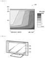
- FIG. 9is a perspective view illustrating an appearance of an application example.
- Embodimentan example in which a sealing layer including a resin material having an oxygen transmission rate higher than a water-vapor transmission rate is provided on an insulating layer
- FIG. 1illustrates a cross-sectional configuration of a display unit (a display unit 1 ) according to an embodiment of the disclosure.
- FIG. 2schematically illustrates a cross-sectional configuration of a main part of the display unit illustrated in FIG. 1 , and this main part is illustrated as a device substrate 2 .
- the display unit 1configures, for example, a large-size display apparatus in which a plurality of display units (display panels) are combined, as represented by a tiling display illustrated in FIG. 6 , and will be hereinafter described as the display unit 1 for convenience.
- a wiring line 42 and a light-emission section 43are provided on a substrate 41 , as illustrated in FIG. 2 .
- the display unit 1has a configuration in which a sealing layer 45 configured of a resin material having an oxygen transmission rate higher than a water-vapor transmission rate is provided on an insulating layer 44 formed to cover the wiring line 42 and the light-emission section 43 .
- a sealing layer 45configured of a resin material having an oxygen transmission rate higher than a water-vapor transmission rate is provided on an insulating layer 44 formed to cover the wiring line 42 and the light-emission section 43 .
- the substrate 41is configured of an organic base material, e.g., a film base material made of a glass-containing resin such as FR4 (a glass epoxy resin) and CEM3 (a glass composite resin).
- the substrate 41is configured of, other than a glass substrate, a plastic substrate of polyether sulfone, polycarbonate, polyimides, polyamides, polyacetals, polyesters (polyethylene terephthalate, polyethylene naphthalate), polyethyl ether ketone, polyolefins, etc., or a metallic foil substrate, on which an insulation surface treatment is performed, of aluminum (Al), nickel (Ni), copper (Cu), stainless steel, etc., or paper.
- a substratein which an insulating resin layer based on polyimide, or epoxy, etc. is formed on a surface of a metal base substrate of Al, etc., and a wiring pattern of the above-described reflective material is printed on this insulating resin layer.
- the wiring line 42is configured of, for example, a simple metal or an alloy of copper (Cu), platinum (Pt), titanium (Ti), ruthenium (Ru), molybdenum (Mo), Cu, tungsten (W), Ni, Al, tantalum (Ta), etc.
- Cuthat has low resistivity, and enables a speedup by reducing a wiring delay time.
- the light-emission section 43is, for example, a solid-state light-emission device that emits light in a predetermined wavelength band from a top surface, and specifically, an LED chip.
- the insulating layer 44covers the wiring line 42 and the light-emission section 43 , and it is preferable to use, for example, a material having light resistance, in order to suppress deterioration attributable to exposure to the light emitted from the light-emission section 43 .
- a material having light resistanceinclude organic insulating materials based on silicone, polyimide, polyacrylate, epoxy, cresol novolac or polystyrene, polyamide, fluorine, etc. It is to be noted that the material to be used for the insulating layer 44 is not limited to the organic insulating materials, and, for example, inorganic insulating materials may be used.
- the sealing layer 45is provided on the insulating layer 44 , and seals the wiring line 42 and the light-emission section 43 , and to suppress entering of moisture into the display unit 1 to be described later.
- the sealing layer 45be made of a material that makes it possible to release gas generated from the substrate 41 , the insulating layer 44 , etc. to outside, while suppressing entering of moisture from outside (a surface).
- the low vapor-transmission filmis preferably such a film that a ratio between a moisture permeability of the substrate 41 and a moisture permeability of the film is small, and, for example, the moisture permeability of the low vapor-transmission film is preferably less than 10 times the moisture permeability of the substrate. This reduces occurrence of ionic migration in the wiring line 42 due to entering of moisture from outside, and suppresses occurrence of a void, etc., due to generation of gas from inside (an organic resin material).
- a material having an oxygen transmission rate (CC/m 2 /24 h/atm; 25° C.) ten times or greater a water-vapor transmission rate (g/m 2 /day, 40° C. 90% RH)is preferable.
- Use of such a materialsuppresses entering of moisture from outside, while moderately releasing gas generated from an organic resin material to outside.
- Table 1provides a water-vapor transmission rate (g/m 2 /day, 40° C.
- FIG. 3illustrates a distribution of a water-vapor transmission rate (g/m 2 /day, 40° C. 90% RH) and an oxygen transmission rate (CC/m 2 /24 h/atm; 25° C.) of each of various resin materials.
- Materials each indicated with a circle illustrated in FIG. 3has a large ratio of the oxygen transmission rate to the water-vapor transmission rate, and the ratio is, for example, 10 or more.
- a more preferable material of the low vapor-transmission filmhas a water-vapor transmission rate of 10 (g/m 2 /day, 40° C. 90% RH) or less and an oxygen transmission rate of 100 (CC/m 2 /24 h/atm; 25° C.) or more, and more desirably has a water-vapor transmission rate of 5 (g/m 2 /day, 40° C. 90% RH) or less and an oxygen transmission rate of 520 (CC/m 2 /24 h/atm; 25° C.) or more.
- examples of a specific material of the low vapor-transmission filminclude a cyclic olefin resin, a nylon resin, a polyethylene resin, etc.
- the sealing layer 45 using the cyclic olefin resinis provided on the insulating layer 44 , a good result is obtained.
- specific examples of the cyclic olefin resininclude an addition polymerization cycloolefin resin and a ring-opening polymerization cycloolefin resin.
- the sealing layer 45may be directly provided on the insulating layer 44 as illustrated in FIG. 2 , or may be provided with an intermediate layer 46 interposed therebetween as illustrated in FIG. 4 .
- the intermediate layer 46is, specifically, formed of a bond or adhesive. In this way, the sealing layer 45 may be fixed (attached) to the insulating layer 44 with the intermediate layer 46 interposed therebetween.
- a wiring line 22 and electronic devicese.g., a light-emission unit 23 (a light-emission section), a driver IC (integrated circuit) 24 , etc., are provided on a substrate 10 , with an insulating layer 21 interposed therebetween, while being covered by an insulating layer 25 . Further, a sealing layer 30 is disposed on the insulating layer 25 .
- the substrate 10 , the wiring line 22 , the light-emission unit 23 , the insulating layer 25 , and the sealing layer 30correspond to the substrate 41 , the wiring line 42 , the light-emission section 43 , the insulating layer 44 , and the sealing layer 45 , respectively, in the device substrate 2 described above. It is to be noted that, in the substrate 10 , a plurality of wiring lines (wiring lines 12 A, 12 B, 15 A, and 15 B), etc., are disposed on a front surface and a back surface of a base material 11 .
- the substrate 10is a so-called multilayered wiring board, in which various kinds of wiring lines are formed inside or on a front surface and a back surface of a film base material made of a glass-containing resin represented by FR4 (a glass epoxy resin), CEM3 (a glass composite resin), etc.
- FR4a glass epoxy resin
- CEM3a glass composite resin
- the base material 11 made of FR4the wiring line 12 A as well as the wiring line 12 B stacked on the front surface of the base material 11 with an insulating layer 13 interposed therebetween
- the wiring line 15 A as well as the wiring line 15 B stacked on the back surface of the base material 11 with an insulating layer 16 interposed therebetweenare provided, for example, the base material 11 made of FR4, the wiring line 12 A as well as the wiring line 12 B stacked on the front surface of the base material 11 with an insulating layer 13 interposed therebetween, and the wiring line 15 A as well as the wiring line 15 B stacked on the back surface of the base material 11 with an insul
- the wiring line 12 A and the wiring line 12 Bare electrically coupled to each other by a bump 14 that penetrates through the insulating layer 13
- the wiring line 15 A and the wiring line 15 Bare electrically coupled to each other by a bump 17 that penetrates through the insulating layer 16
- the wiring line 12 A and the wiring line 15 Aare electrically coupled to each other, with a through electrode 18 interposed therebetween and penetrating through the base material 11 .
- an insulating layer 19is provided as a protective film. In the insulating layer 19 , for example, an opening 19 A to couple the wiring line 15 B and an external circuit (not illustrated) is provided at any position.
- the wiring lines 12 A, 12 B, 15 A, and 15 Bare provided in a selective region on the base material 11 , and configured of, for example, a simple metal or an alloy of copper (Cu), platinum (Pt), titanium (Ti), ruthenium (Ru), molybdenum (Mo), Cu, tungsten (W), Ni, Al, tantalum (Ta), etc.
- Cucopper
- Ptplatinum
- Tititanium
- Ruruthenium
- Momolybdenum
- Cuthat has low resistivity, and enables a speedup by reducing a wiring delay time.
- two or more kinds of thesemay be stacked and used. It is possible to use a material similar to that of the wiring lines 12 A, 12 B, 15 A, and 15 B, also for the bumps 14 and 17 as well as the through electrode 18 .
- the insulating layers 13 , 16 , and 19are formed of, for example, a material including one or more kinds of silicon oxide (SiO), silicon nitride (SiN), silicon oxynitride (SiON), hafnium oxide (HfO), aluminum oxide (AlO), aluminum nitride (AlN), tantalum oxide (TaO), zirconium oxide (ZrO), hafnium oxynitride, hafnium silicon oxynitride, aluminum oxynitride, tantalum oxynitride, and zirconium oxynitride.
- the insulating layers 13 , 16 , and 19may each have a single-layered structure, or may have a layered structure using, for example, two or more kinds of materials such as a SiN film and a SiO film.
- the insulating layers 13 , 16 , and 19are each patterned into a predetermined shape by etching after coating formation, but a pattern may be formed by a printing technique such as ink jet printing, screen printing, offset printing, and gravure printing, depending on the material.
- the insulating layer 21prevents a short circuit between the wiring line 15 B and the wiring line 22 . It is preferable to use a material having light resistance, as a material of the insulating layer 21 . Examples of this material include the materials enumerated above for the insulating layer 44 , e.g., organic insulating materials based on silicone, polyimide, polyacrylate, epoxy, cresol novolac, polystyrene, polyamide, fluorine, etc. Besides, the materials enumerated for the insulating layers 13 , 16 , and 19 may also be used.
- the wiring line 22it is possible to use the materials enumerated above for the wiring lines 12 A, 12 B, 15 A, and 15 B.
- the wiring line 22may use the same material as that of 12 A, 12 B, 15 A, and 15 B, or may use a material different therefrom. In particular, it is preferable to use Cu. It is to be noted that it is possible to form the wiring lines 12 A, 12 B, 15 A, and 15 B as well as the wiring line 22 , by, for example, plating, various vapor deposition methods, or sputtering.
- the light-emission unit 23includes, for example, a plurality of solid-state light-emission devices that emit the respective pieces of light in wavelength bands different from each other, from the respective top surfaces.
- FIG. 5Aperspectively illustrates an example of a schematic configuration of the light-emission unit 23 .
- FIG. 5Billustrates an example of a cross-sectional configuration in I-I arrow direction of the light-emission unit 23 in FIG. 5A .
- Light-emission devices 23 AR, 23 AG and 23 ABare each a solid-state light-emission device that emits light in a predetermined wavelength band from a top surface, and specifically, an LED chip.
- the LED chiprefers to a chip in a state of being cut out from a wafer used for crystal growth, and refers to an LED chip that this is not a package type covered by a molded resin, etc.
- the LED chipis, for example, of a size of 5 ⁇ m or more and 100 mm or less, and is a so-called micro LED.
- the LED chiphas a planar shape, which is, for example, substantially square.
- the LED chipis a thin piece, and has an aspect ratio (height/width) of, for example, 0.1 or more and less than 1.
- the light-emission devices 23 AR, 23 AG and 23 ABare each disposed inside the light-emission unit 23 , and, for example, as illustrated in FIG. 5A , the light-emission devices 23 AR, 23 AG and 23 AB are arranged in a line with a predetermined clearance therebetween.
- the light-emission unit 23has, for example, an elongated shape extending in an array direction of the light-emission devices 23 AR, 23 AG and 23 AB.
- the clearance between adjacent ones of the light-emission devices 23 AR, 23 AG and 23 ABis, for example, equal to or greater than the size of each of the light-emission devices 23 AR, 23 AG and 23 AB. It is to be noted that the above-described clearance may be narrower than the size of each of the light-emission devices 23 AR, 23 AG and 23 AB in some cases.
- the light-emission devices 23 AR, 23 AG and 23 ABemit the respective pieces of light in wavelength bands different from each other.
- the light-emission device 23 AGis a light-emission device that emits light in a green light band
- the light-emission device 23 ARis a light-emission device that emits light in a red color band
- the light-emission device 23 ABis a light-emission device that emits light in a blue color band.
- the light-emission unit 23has an elongated shape extending in the array direction of the light-emission devices 23 AR, 23 AG and 23 AB.
- the light-emission device 23 AGis disposed, for example, in proximity to a short side of the light-emission unit 23
- the light-emission device 23 ABis disposed, for example, in proximity to a short side, which is different from the short side close to the light-emission device 23 AG between the short sides of the light-emission unit 23
- the light-emission device 23 ARis disposed, for example, between the light-emission device 23 AG and the light-emission device 23 AB.
- each of the light-emission devices 23 AR, 23 AG and 23 ABis not limited to that described above, but a positional relationship of other component may be described below assuming that the light-emission devices 23 AR, 23 AG and 23 AB are disposed at the respective positions exemplified above.
- the light-emission devices 23 AR, 23 AG and 23 ABeach have, for example, a semiconductor layer in which a first conductive layer, an active layer, and a second conductive layer are stacked in this order (none of which is illustrated).
- the first conductive layer, the active layer, and the second conductive layerare configured of, for example, an InGaN-based semiconductor material.
- the first conductive layer, the active layer, and the second conductive layerare configured of, for example, an AlGaInP-based semiconductor material.
- An upper electrode 52is provided on a top surface (a light extraction face S 2 ) of the second conductive layer.
- the upper electrode 52is made of titanium (Ti)/platinum (Pt)/gold (Au), for example, in the light-emission devices 23 AG and 23 AB.
- the upper electrode 52is made of a gold-germanium alloy (AuGe)/nickel (Ni)/Au, for example, in the light-emission device 23 AR.
- the upper electrode 52is in contact with the second conductive layer, and electrically coupled to the second conductive layer. In other words, the upper electrode 52 is in ohmic contact with the second conductive layer.
- a lower electrode 51is provided on an undersurface (a back face S 1 ) of the first conductive layer.
- the lower electrode 51is a metal electrode.
- the lower electrode 51is made of Ti/Pt/Au, for example, in the light-emission devices 23 AG and 23 AB.
- the lower electrode 51is made of AuGe/Ni/Au, for example, in the light-emission device 23 AR.
- the lower electrode 51is in contact with the first conductive layer, and electrically coupled to the first conductive layer. In other words, the lower electrode 51 is in ohmic contact with the first conductive layer.
- the lower electrode 51 and the upper electrode 52may both be configured of a single electrode, or may be configured of a plurality of electrodes.
- the lower electrode 51 and the upper electrode 52may include, for example, a metallic material having high reflectivity, such as silver (Ag) and aluminum (Al).
- An insulator 50surrounds the light-emission devices 23 AR, 23 AG and 23 AB at least from side-surface side of the light-emission devices 23 AR, 23 AG and 23 AB, and holds these devices.
- the insulator 50is configured of, for example, a resin material such as silicone, acrylic, and epoxy.
- the insulator 50may include other material such as polyimide, in a portion thereof.
- the insulator 50is formed in contact with the side surface of each of the light-emission devices 23 AR, 23 AG and 23 AB, and the top surface of each of the light-emission devices 23 AR, 23 AG and 23 AB.
- the insulator 50has an elongated shape (e.g., a rectangular parallelepiped shape) extending in the array direction of the light-emission devices 23 AR, 23 AG and 23 AB.
- the insulator 50has a height more than a height of the light-emission device 23 AR, 23 AG and 23 AB, and the insulator 50 has a width (a width in the short-side direction) more than a width of the light-emission devices 23 AR, 23 AG, and 23 AB.
- the insulator 50in itself has a size of, for example, 1 mm or less.
- the insulator 50is a thin piece.
- the insulator 50has an aspect ratio (maximum height/maximum width) small enough to avoid the light-emission unit 23 lying during transfer of the light-emission unit 23 , and is, for example, 1 ⁇ 5 or less.
- the driver IC 24is, for example, a semiconductor device in which a circuit is formed on a surface of a semiconductor substrate (an Si substrate) by utilizing a semiconductor-circuit formation technique.
- the light-emission unit 23 and the driver IC 24may each be a single device, or may be contained in a package, or may be molded by resin, etc., to be a chip component, as described above.
- the insulating layer 25 and the sealing layer 30 described aboveare provided.
- examples of a materialinclude the materials enumerated above for the insulating layer 44 , e.g., organic insulating materials based on silicone, polyimide, polyacrylate, epoxy, cresol novolac or polystyrene, polyamide, fluorine, etc.
- the materials enumerated for the insulating layers 13 , 16 , and 19may be used.
- examples of a materialinclude the materials enumerated above for the insulating layer 44 , and materials having a large ratio, e.g., 10 or more, of an oxygen transmission rate to a water-vapor transmission rate, e.g., a cyclic olefin resin, a nylon resin, a polyethylene resin, etc.
- the sealing layer 30has a thickness of, preferably, for example, around 100 ⁇ m, and is, for example, 10 ⁇ m or more and 300 ⁇ m or less.
- the sealing layer 30In a case where the sealing layer 30 is too thin, it is difficult to protect a wiring line and a light source, and in a case where the sealing layer 30 is thick, there is a possibility that a display viewing angle property may deteriorate due to vignetting of light emission at an end face.
- the display unit 1 in the present embodimentis not provided with a peripheral circuit, a sealing section, etc. provided at a peripheral edge portion in an ordinary display unit, and has a similar layered structure on the entire surface of the substrate 10 .
- the layered structure of the insulating layer 25 and the sealing layer 30 on the substrate 10 of the display unit 1extends to an end face of the substrate 10 .
- FIG. 6illustrates an overall configuration of a tiling display, in which the display unit 1 of the disclosure is provided as each of a plurality of display panels combined (here, a total of four display panels 3 A, 3 B, 3 C, and 3 D).
- the display panels 3 A to 3 Deach have a configuration similar to that of the display unit 1 described above.
- the display panels 3 A to 3 Dare arranged, for example, two-dimensionally, in a 2 ⁇ 2 region, and it is possible to display an image by combining display regions of the respective display panels 3 A to 3 D.
- “A” and “B” and orientations thereof in FIG. 6schematically represent a type and an arrangement state of a backplane used. The type and layout of the backplane used in each of the display panels 3 A to 3 D will be described later.
- the driver IC 24 for display drivingis coupled to each of the display panels 3 A to 3 D.
- a signal-line driving circuit 120 A and a scanning-line driving circuit 130 Aare implemented by, for example, a COF (Chip on film) 140 .
- these driver ICsmay be directly formed (built) in the display panel 3 A, or may be implemented by other technique, e.g., COG (Chip on glass).
- a power-line driving circuit(not illustrated) is additionally coupled to the display panel 3 A.
- a signal-line driving circuit 120 B and a scanning-line driving circuit 130 Bare coupled through the COF 140 , as with the display panel 3 A.
- a signal-line driving circuit 120 C and a scanning-line driving circuit 130 Care coupled to the display panel 3 C through the COF 140
- a signal-line driving circuit 120 D and a scanning-line driving circuit 130 Dare coupled to the display panel 3 D through the COF 140 .
- a drive control section 110includes, for example, a timing controller 111 , and gamma adjustment sections 112 a to 112 d.
- the display panels 3 A to 3 Deach have a plurality of pixels P disposed in a matrix. Active matrix driving of each of the pixels P is performed by display driving by the signal-line driving circuits 120 A to 120 D and the scanning-line driving circuits 130 A to 130 D, and the display panels 3 A to 3 D each thereby perform image display on the basis of the image signal Din inputted from outside. It is to be noted that, in each of the figures, the quantity, pitch, size, etc., of the pixels P and terminal sections 130 to be described later are illustrated in a simple manner for convenience of description, and different from actual ones.
- the display panels 3 A to 3 Deach have a plane shape of, for example, a rectangle or square (here, rectangle).
- the display panels 3 A to 3 Dare disposed next to each other to be shaped like tiles as a whole. Specifically, the display panels 3 A to 3 D are laid edge to edge, for example, on a housing or substrate, etc. not illustrated.
- a region formed by combining the display regions of the respective display panels 3 A to 3 Dis a display region (a display region 100 ) of the display unit 1 . It is to be noted that the description will be provided below using the display panel 3 A as a representative example, in a case where the display panels 3 A to 3 D are not distinguished from each other in particular.
- FIG. 7Aillustrates a configuration of a backplane 41 A
- FIG. 7Billustrates a configuration of a backplane 41 B
- the backplane 41 Ahas a pixel circuit 150 for each of the pixels P, in a region (a region 10 A) corresponding to a portion of the display region 100 .
- the plurality of pixel circuits 150are two-dimensionally arranged in the backplane 41 A.
- the terminal section 130 for implementationis disposed in regions X 1 and Y 1 along rectangular two sides of a peripheral region of a formation region (i.e., the region 10 A) of the pixel circuits 150 .
- the plurality of terminal sections 130are disposed along the two sides on left side and upper side among four rectangular sides arranged right, left, upper, and lower sides.
- the terminal section 130is a pad for wiring connection to each of circuits including the signal-line driving circuits 120 A to 120 D or the scanning-line driving circuits 130 A to 130 D.
- the backplane 41 Bhas the pixel circuit 150 for each of the pixels P in a region (a region 23 AB 10 B) corresponding to a portion of the display region 100 (the plurality of pixel circuits 150 are two-dimensionally arranged in the backplane 41 B).
- the terminal section 130 for implementationis disposed in regions X 2 and Y 2 along two rectangular sides of a peripheral region of a formation region (i.e., the region 23 AB) of the pixel circuits 150 .
- the plurality of terminal sections 130are disposed, for example, along two sides on left side and lower side among four of right, left, upper, and lower rectangular sides.
- the backplanes 41 A and 11 B 41 Bare different in terms of, for example, a layout (for example, positions) of the terminal sections 130 .
- the backplane 41 Ais disposed, for example, in each of the display panels 3 A and 3 D, and the backplane 41 B is disposed in each of the display panels 3 A and 3 C.
- the backplane 41 Ais used for a pair of the display panels 3 A and 3 D as backplanes of the same type
- the backplane 41 Bis used for a pair of the display panels 3 A and 3 C as backplanes of the same type.
- the “types” of the backplaneare distinguished from each other, for example, depending on the layout of the pixel circuits 150 and the terminal sections 130 , and the “same type” means that, for example, the layouts in terms of the pixel circuits 150 and the terminal sections 130 are substantially the same.
- backplanessuffice as long as these backplanes are almost equal in terms of the positions, shapes, quantity, etc. of the pixel circuits 150 and the terminal sections 130 , and may have some errors in design, and backplanes in which local layout modifications are made, etc. are also included.
- the timing controller 111 of the drive control section 110controls, for example, each of circuits including the signal-line driving circuits 120 A to 120 D and the scanning-line driving circuits 130 A to 130 D to operate in conjunction with each other.
- the timing controller 111outputs, for example, a control signal to each of the above-described circuits, in response to the image signal Din inputted from outside.
- the gamma adjustment sections 112 a to 112 dare individually provided for the display panels 3 A to 3 D, respectively.
- the gamma adjustment sections 112 a to 112 deach perform, for example, a gamma adjustment (a gamma correction) on the digital image signal Din inputted from outside, and output a thus-obtained image signal to the signal-line driving circuits 120 A to 120 D.
- the gamma adjustment section 112 amakes a gamma adjustment to the display panel 3 A
- the gamma adjustment section 112 bmakes a gamma adjustment to the display panel 3 B
- the gamma adjustment section 112 cmakes a gamma adjustment to the display panel 3 C
- the gamma adjustment section 112 dmakes a gamma adjustment to the display panel 3 D.
- signal processing other than the gamma adjustmente.g., an overdrive correction may be performed.
- the signal-line driving circuits 120 A to 120 Dapply, to each of signal lines DTL, analog signal voltages corresponding to the image signals input from the gamma adjustment sections 112 a to 112 d , in response to the control signal from the timing controller 111 , for example.
- the scanning-line driving circuits 130 A to 130 Deach select, for example, a plurality of scanning lines WSL sequentially for each predetermined unit, in response to the control signal from the timing controller 111 .
- the scanning-line driving circuits 130 A to 130 Deach effect execution of Vth correction, signal-voltage writing, ⁇ correction, etc. in a desired order, by selecting one or more of the scanning lines WSL in a predetermined sequence.
- the Vth correctionrefers to a correction operation of bringing a voltage Vgs held between a gate and a source of a drive transistor Tr 1 close to a threshold voltage of a drive transistor.
- the signal-voltage writingrefers to an operation of writing a signal voltage to the gate of the drive transistor Tr 1 through a write transistor Tr 2 .
- the ⁇ correctionrefers to an operation of correcting the voltage Vgs held between the gate and the source of the drive transistor Tr 1 , depending on a size of a mobility ⁇ of the drive transistor Tr 1 .
- measures for suppressing the occurrence of the ionic migrationinclude increasing a wiring interval, lowering a voltage between wiring lines, reducing remaining ions in a resin that couple to copper (Cu) serving as a wiring material, and providing a member that suppresses entering of moisture from outside.
- a wiring interval, a voltage, and a resin materialare determined by other factors in designing a device in many cases and thus, it is difficult to make a modification for suppression of the occurrence of the ionic migration.
- providing a member of suppressing entering of moisture from outsideis selected as a measure for suppressing the occurrence of the ionic migration, and there is manufactured a display unit in which a barrier layer (an inorganic barrier layer) made of an inorganic material is deposited on a substrate, or an inorganic barrier film is attached.
- a multilayered wiring boardin which a wiring layer forming various wiring lines is multilayered to improve such a signal delay and a decrease in manufacturing yield, and in which, to avoid a signal delay due to the formation of the multilayer, density of the wiring layer is increased and a footprint of an electronic component is increased using an insulating layer, which is made of an organic resin, etc. having a low dielectric constant, between the wiring layers.
- the multilayered wiring boardincludes, for example, a base material having an insulation property, and an organic resin material such as epoxy resin.
- a substrate (an organic substrate) formed using an organic resin materialeasily absorbs and transmits moisture, as compared with a substrate (an inorganic substrate) formed from an inorganic material such as a glass or silicon substrate.
- a water-vapor transmission rate (WVTR)varies depending on quality of a material, a wiring pattern, the number of stacked layers of wiring lines formed inside, etc., but is approximately in a range of 10 to 20 g/m 2 /day, and a water absorption rate is about 1%, which is not small.
- moisturenot only enters from a direction perpendicular to a substrate surface, but also enters from an end face.
- there is a cleaning process in photolithography, etc. used in forming the wiring line and the insulating layerand moisture is easily absorbed into the substrate in this process. For this reason, it is necessary to sufficiently dry the organic substrate before providing an inorganic barrier layer.
- sufficiently reducing entering of moisture into the organic substrateis not achievable by merely providing the inorganic barrier layer on the organic substrate.
- FIG. 8illustrates a simulation of a moisture entering distribution in a case where a device substrate 200 , in which an inorganic barrier layer 450 is provided on a glass-epoxy substrate used as a base material of a multilayered wiring board, is left at a high temperature and a high humidity for a predetermined length of time.
- the device substrate 200has a configuration in which a wiring line and a light-emission unit (a wiring layer) are provided on the glass-epoxy substrate, these are covered by an insulating material having a moisture permeability equal to that of the glass-epoxy substrate, and the inorganic barrier layer 450 is provided on a surface thereof.
- a wiring line and a light-emission unita wiring layer
- the multilayered wiring boardin terms of property of an organic resin material that is a base material, the multilayered wiring board easily contains moisture, and gas is easily generated inside a substrate.
- an inorganic barrier layer having a high barrier propertyis provided on a surface of the multilayered wiring board, the moisture contained in the substrate and the gas generated from the organic resin material are trapped and thus, there is a possibility that a void occurs due to feeling off of an interface having weak adhesion.
- entering of moistureis prevented by providing the inorganic barrier layer on the surface of the multilayered wiring board, there is such an issue that sufficient waterproofing effects are not obtainable and moreover, a film is caused to peel off.
- the sealing layer 30 including the resin material having the oxygen transmission rate higher than the water-vapor transmission rateis provided on the insulating layer 25 that covers the wiring line 22 , the light-emission unit 23 , etc. provided on the substrate 10 .
- Table 2provides occurrence of ionic migration between wiring lines and occurrence of a void in a high-temperature high-humidity environment, in a comparison between a case where the sealing layer 30 formed of a resin material (e.g., a cyclic olefin resin) having an oxygen transmission rate higher than a water-vapor transmission rate is provided on the insulating layer 25 that covers the wiring line 22 , the light-emission unit 23 , etc., and a case where an inorganic barrier layer is provided in place of the sealing layer 30 .
- the high-temperature high-humidity environmentis an environment with a temperature of 60° C. and a humidity of 90%. In this way, forming the sealing layer 30 by using the cyclic olefin resin makes it possible to moderately diffuse, to outside, moisture contained in the substrate and gas likely to be generated from the organic resin material of the substrate 10 .
- the sealing layer 30 including the resin material having the oxygen transmission rate higher than the water-vapor transmission rateis provided on the insulating layer 25 that covers the wiring line 22 , the light-emission unit 23 , etc. provided on the substrate 10 .
- the display unit 1(and the tiling display including this unit) described in the above-described embodiment is applicable to display units of electronic apparatuses in various fields that display image signals inputted from outside or image signals generated inside, as a still image or a moving image.
- Examples of the electronic apparatusesinclude television apparatuses, digital cameras, laptop personal computers, mobile terminals such as mobile phones, video cameras, etc. Examples thereof will be described below.
- FIG. 8illustrates an appearance of a television apparatus to which the display unit 1 of the above-described embodiment is applied.
- This television apparatushas, for example, an image-display screen section 300 including a front panel 310 and a filter glass 320 .
- the above-described display unit 1is applied to the image-display screen section 300 .
- the disclosureis described above by referring to the embodiment and the modification example, but the disclosure is not limited to the above-described embodiment and modification example, and various modifications may be made.
- the material and thickness, or the film formation method and film formation conditions of each of the layers, or the disconnection and repair for short circuit defects, etc. described in the above-described embodimentare not limitative.
- Other material and thickness, or film formation method and film formation conditions, or disconnection and repairing methodmay be adopted.
- the light-emission unit 23is used as the electronic device, but, for example, a photodetector may be used.
- a display unitincluding:
- a sealing layerprovided on an entire surface of the insulating layer, and including a resin material having an oxygen transmission rate higher than a water-vapor transmission rate.
- the resin materialcomprises a cyclic olefin resin, a nylon resin, or a polyethylene resin.
- cyclic olefin resincomprises an addition polymerization cycloolefin resin or a ring-opening polymerization cycloolefin resin.
- the display unit according to any one of (1) to (5)in which a layered structure having the wiring line and the light-emission section that are provided on the substrate, the insulating layer, and the sealing layer in this order extends to an end face of the substrate.
- the display unit according to any one of (1) to (6)in which the insulating layer is attached to the insulating layer with an intermediate layer interposed therebetween.
- the organic base materialcomprises a polyester resin, an epoxy resin, or a polyimide resin.
Landscapes
- Engineering & Computer Science (AREA)
- Microelectronics & Electronic Packaging (AREA)
- Physics & Mathematics (AREA)
- General Physics & Mathematics (AREA)
- Power Engineering (AREA)
- Computer Hardware Design (AREA)
- Condensed Matter Physics & Semiconductors (AREA)
- Theoretical Computer Science (AREA)
- Mechanical Engineering (AREA)
- Electroluminescent Light Sources (AREA)
- Devices For Indicating Variable Information By Combining Individual Elements (AREA)
- Laminated Bodies (AREA)
Abstract
Description
| TABLE 1 | ||||
| Oxygen | ||||
| Water-vapor | transmission | Carbon-dioxide | ||
| Film | transmission | rate | transmission rate | |
| thickness | rate (g/m2/day, | (CC/m2/24 h/ | (CC/m2/24 h/ | |
| (μm) | 40° C. 90% RH) | atm, 25° C.) | atm, 25° C.) | |
| Ethylene-vinylalcohol | 15 | 120 | 0.2 | 1.1 |
| copolymer | ||||
| (ethylene 56%) | ||||
| Acrylonitrile copolymer | 25 | 82 | 12 | 25 |
| (acrylonitrile 70%) | ||||
| Vinylidene chloride | 25 | 3 | 16 | 13 |
| copolymer | ||||
| Nylon 6 | 20 | 220 | 85 | 450 |
| Nylon 66 | 25 | 60 | 77 | 140 |
| Nylon 11 | 25 | 8 | 520 | 2,300 |
| Nylon 12 | 25 | 1 | 1,100 | 3,200 |
| Polyethylene | 12 | 55 | 64 | 175 |
| terephthalate | ||||
| (biaxial stretching) | ||||
| Polyethylene | 30 | 45 | 43 | 430 |
| terephthalate | ||||
| Polyester (PETG) | 50 | 30 | 50 | 150 |
| Polyarylate (terephthalic | 30 | 47 | 86 | 660 |
| acid-bisphenol A | ||||
| polycondensate) | ||||
| Polyurethane 25 | 25 | 850 | 2,700 | 14,000 |
| Polyvinyl chloride | 25 | 45 | 125 | 760 |
| (nonplasticized) | ||||
| Polyvinyl chloride | 50 | 40 | 1,820 | 120,000 |
| (plasticizer 30%) | ||||
| Polycarbonate | 50 | 24 | 1,800 | 10,100 |
| Polystyrene | 25 | 120 | 8,100 | 37000 |
| Polychloro- | 25 | 1 | 26 | 180 |
| trifluoroethylene | ||||
| Polytetrafluoroethylene | 25 | 5 | 17,600 | 48000 |
| Polyvinyl fluoride | 50 | 50 | 260 | |
| Polyimide | 25 | 96 | 390 | 620 |
| Polyethylene | 25 | 5 | 2,900 | 7,600 |
| (density 0, 955) | ||||
| Polypropylene 20 | 20 | 15 | 8100 | 37000 |
| Poly-4- | 50 | 55 | 32,000 | 95000 |
| methylpentene-1 | ||||
| Ionomer 25 | 25 | 31 | 7,700 | |
| Polysulfone | 25 | 280 | 3,500 | 14,000 |
| Cellulose triacetate | 25 | 900 | 2,300 | 12,600 |
| Ethyl cellulose 25 | 25 | 108 | 35,000 | 80,000 |
| COC | 25 | 3.2 | 800 | |
| COC | 100 | 0.8 | 200 | |
| COP | 100 | 1 | ||
| TABLE 2 | ||
| Occurrence of ionic | ||
| migration between wiring | ||
| lines at application of | Occurrence of void at | |
| voltage in 60° C. 90% | application of voltage in | |
| environment | 60° C. 90% environment | |
| Cyclic olefin resin | 500 hours or more | None |
| Film with barrier | Several tens of hours | Void occurred |
| inorganic film | ||
(7) The display unit according to any one of (1) to (6), in which the insulating layer is attached to the insulating layer with an intermediate layer interposed therebetween.
(8) The display unit according to (7), in which the intermediate layer comprises an adhesive layer or a bonding layer.
(9) The display unit according to any one of (1) to (8), in which the light-emission section comprises a light-emitting diode.
(10) The display unit according to any one of (1) to (9), in which the substrate includes an organic base material.
(11) The display unit according to (10), in which the organic base material comprises a polyester resin, an epoxy resin, or a polyimide resin.
Claims (10)
Applications Claiming Priority (4)
| Application Number | Priority Date | Filing Date | Title |
|---|---|---|---|
| JPJP2015-123611 | 2015-06-19 | ||
| JP2015-123611 | 2015-06-19 | ||
| JP2015123611AJP2017009725A (en) | 2015-06-19 | 2015-06-19 | Display device |
| PCT/JP2016/066900WO2016204024A1 (en) | 2015-06-19 | 2016-06-07 | Display device |
Publications (2)
| Publication Number | Publication Date |
|---|---|
| US20180166615A1 US20180166615A1 (en) | 2018-06-14 |
| US11247439B2true US11247439B2 (en) | 2022-02-15 |
Family
ID=57545896
Family Applications (1)
| Application Number | Title | Priority Date | Filing Date |
|---|---|---|---|
| US15/580,942Active2036-09-11US11247439B2 (en) | 2015-06-19 | 2016-06-07 | Display unit |
Country Status (3)
| Country | Link |
|---|---|
| US (1) | US11247439B2 (en) |
| JP (1) | JP2017009725A (en) |
| WO (1) | WO2016204024A1 (en) |
Cited By (3)
| Publication number | Priority date | Publication date | Assignee | Title |
|---|---|---|---|---|
| US20210159166A1 (en)* | 2019-11-22 | 2021-05-27 | Renesas Electronics Corporation | Semiconductor device |
| US20240257716A1 (en)* | 2023-01-31 | 2024-08-01 | Lg Display Co., Ltd. | Display device |
| US12417720B2 (en)* | 2021-09-09 | 2025-09-16 | Kyocera Corporation | Display device and multi-display |
Families Citing this family (11)
| Publication number | Priority date | Publication date | Assignee | Title |
|---|---|---|---|---|
| JP2017009725A (en)* | 2015-06-19 | 2017-01-12 | ソニー株式会社 | Display device |
| KR102305180B1 (en) | 2017-04-25 | 2021-09-28 | 주식회사 루멘스 | Micro led display apparatus and method for fabricating the same |
| WO2019014036A1 (en)* | 2017-07-11 | 2019-01-17 | Corning Incorporated | Tiled displays and methods of manufacturing the same |
| KR102569728B1 (en)* | 2017-12-08 | 2023-08-23 | 엘지디스플레이 주식회사 | Micro led display device whitout bezzel |
| CN112119509B (en) | 2018-05-24 | 2021-08-24 | 大日本印刷株式会社 | Sealing material sheet for self-luminous display or direct type backlight, self-luminous display, direct type backlight |
| JP2020020971A (en) | 2018-08-01 | 2020-02-06 | Necディスプレイソリューションズ株式会社 | Display system and display system control method |
| CN112996657A (en)* | 2018-12-10 | 2021-06-18 | 日本瑞翁株式会社 | Laminate, method for producing same, circularly polarizing plate, display device, and touch panel |
| KR20210025746A (en) | 2019-08-27 | 2021-03-10 | 삼성디스플레이 주식회사 | Backlight unit and display device having the same |
| CN212648273U (en)* | 2020-07-29 | 2021-03-02 | 隆达电子股份有限公司 | LED device |
| US12094861B2 (en) | 2020-09-18 | 2024-09-17 | Lextar Electronics Corporation | Light emitting array structure and display |
| KR20230103654A (en) | 2021-12-31 | 2023-07-07 | 엘지디스플레이 주식회사 | Tiling Display Device |
Citations (137)
| Publication number | Priority date | Publication date | Assignee | Title |
|---|---|---|---|---|
| US6184477B1 (en)* | 1998-12-02 | 2001-02-06 | Kyocera Corporation | Multi-layer circuit substrate having orthogonal grid ground and power planes |
| US20010040645A1 (en)* | 2000-02-01 | 2001-11-15 | Shunpei Yamazaki | Semiconductor device and manufacturing method thereof |
| US20020030189A1 (en)* | 2000-09-14 | 2002-03-14 | Akira Ishikawa | Semiconductor device and manufacturing method thereof |
| US20020044111A1 (en)* | 2000-05-12 | 2002-04-18 | Semiconductor Energy Laboratory Co., Ltd. | Light-emitting device and electric appliance |
| US6518600B1 (en)* | 2000-11-17 | 2003-02-11 | General Electric Company | Dual encapsulation for an LED |
| US20030034497A1 (en)* | 2001-06-20 | 2003-02-20 | Semiconductor Energy Laboratory Co., Ltd. | Light emitting device and method of manufacturing the same |
| US20030057422A1 (en)* | 2001-06-20 | 2003-03-27 | Semiconductor Energy Laboratory Co., Ltd. | Light emitting device and electronic apparatus |
| JP2003115613A (en) | 2001-08-01 | 2003-04-18 | Sony Corp | Image display device and method of fabricating the same |
| US6577367B2 (en)* | 2000-01-12 | 2003-06-10 | Lg. Philips Lcd Co., Ltd | Array substrate for a liquid crystal display device and method for fabricating the same |
| US20040226745A1 (en)* | 1999-08-06 | 2004-11-18 | Ibiden Co., Ltd. | Electroplating solution, method for manufacturing multilayer printed circuit board using the same solution, and multilayer printed circuit board |
| US20040232418A1 (en)* | 2003-05-21 | 2004-11-25 | Semiconductor Energy Laboratory Co., Ltd. | Light emitting device and manufacturing method of the same |
| US20050140265A1 (en)* | 2003-12-26 | 2005-06-30 | Semiconductor Energy Laboratory Co., Ltd. | Display device and method for manufacturing display device |
| JP2006024530A (en) | 2004-07-09 | 2006-01-26 | Sharp Corp | Display device and manufacturing method thereof |
| US20060046336A1 (en)* | 2004-08-30 | 2006-03-02 | Semiconductor Energy Laboratory Co., Ltd. | Method for manufacturing display device |
| US20060076694A1 (en)* | 2004-10-13 | 2006-04-13 | Taiwan Semiconductor Manufacturing Co., Ltd. | Semiconductor device package with concavity-containing encapsulation body to prevent device delamination and increase thermal-transferring efficiency |
| JP2006127815A (en) | 2004-10-26 | 2006-05-18 | Sekisui Chem Co Ltd | Organic electroluminescent element |
| US20060132401A1 (en)* | 2000-06-12 | 2006-06-22 | Semiconductor Energy Laboratory Co., Ltd. | Light emitting module and method of driving the same, and optical sensor |
| JP2006334909A (en) | 2005-06-01 | 2006-12-14 | Gunze Ltd | Film with gas barrier layer |
| US20070036927A1 (en)* | 2004-04-16 | 2007-02-15 | Asahi Glass Company, Limited | Laminate tube |
| JP2007273498A (en) | 2006-03-30 | 2007-10-18 | Kyocera Corp | Wavelength converter and light emitting device |
| US20080067932A1 (en)* | 2006-09-15 | 2008-03-20 | Ji-Yeon Baek | Organic light emitting display and method of fabricating the same |
| WO2008032526A1 (en) | 2006-09-15 | 2008-03-20 | Konica Minolta Holdings, Inc. | Process for production of flexible sealing film and organic electroluminescent devices made by using the film |
| JP2008226471A (en) | 2007-03-08 | 2008-09-25 | Konica Minolta Holdings Inc | Manufacturing method of organic electroluminescent panel and organic electroluminescent panel |
| US20090039762A1 (en)* | 2004-01-02 | 2009-02-12 | Jun-Kyu Park | White led device comprising dual-mold and manufacturing method for the same |
| US20090058763A1 (en)* | 2007-08-30 | 2009-03-05 | Sony Corporation | Display apparatus |
| JP2009081122A (en) | 2007-09-06 | 2009-04-16 | Fujifilm Corp | Method for producing organic EL element sealed with gas barrier film and organic EL element sealed with gas barrier film |
| US20090104443A1 (en)* | 2006-03-27 | 2009-04-23 | Fujifilm Corporation | Film laminate, production method thereof, and optically-compensatory film, polarizing plate, polarizing plate protective film and liquid crystal display using the same |
| US7530167B2 (en)* | 2003-01-30 | 2009-05-12 | Endicott Interconnect Technologies, Inc. | Method of making a printed circuit board with low cross-talk noise |
| US20100096633A1 (en)* | 2008-10-16 | 2010-04-22 | Semiconductor Energy Laboratory Co., Ltd. | Flexible light-emitting device, electronic device, and method for manufacturing flexible-light emitting device |
| US20100140638A1 (en)* | 2006-11-15 | 2010-06-10 | Hitachi Chemical Co., Ltd. | Thermosetting resin composition for light reflection, method for manufacturing the resin composition and optical semiconductor element mounting substrate and optical semiconductor device using the resin composition |
| US20100155739A1 (en)* | 2005-08-04 | 2010-06-24 | Masafumi Kuramoto | Light-emitting device, method for manufacturing same, molded body and sealing member |
| US20100171138A1 (en)* | 2009-01-08 | 2010-07-08 | Semiconductor Energy Laboratory Co., Ltd. | Light Emitting Device and Electronic Device |
| US20100207851A1 (en)* | 2009-02-17 | 2010-08-19 | Cok Ronald S | Chiplet driver pairs for two-dimensional display |
| US20100213490A1 (en)* | 2009-02-24 | 2010-08-26 | Il Woo Park | Sealing composition for light emitting device and light emitting device including the same |
| US20100253215A1 (en)* | 2009-04-01 | 2010-10-07 | Seiko Epson Corporation | Organic electroluminescence device |
| US20100273927A1 (en)* | 2009-04-24 | 2010-10-28 | Taguchi Yusuke | Silicone resin composition for optical semiconductor devices and an optical semiconductor device |
| US20100301473A1 (en)* | 2007-11-01 | 2010-12-02 | Dai Nippon Printing Co., Ltd. | Component built-in wiring board and manufacturing method of component built-in wiring board |
| US20100320215A1 (en)* | 2007-11-22 | 2010-12-23 | Mitsubishi Tanabe Pharma Corporation | plastic container comprising cyclic polyolefin layer |
| US20110157762A1 (en)* | 2009-12-28 | 2011-06-30 | Sony Corporation | Capacitive input device and electro-optical apparatus with input function |
| US20110211348A1 (en)* | 2010-04-01 | 2011-09-01 | Kyong Jun Kim | Light emitting device package and lighting system |
| US20110297942A1 (en)* | 2010-06-03 | 2011-12-08 | Samsung Mobile Display Co., Ltd. | Organic light-emitting display device and method of manufacturing the same |
| US20120074838A1 (en)* | 2010-09-28 | 2012-03-29 | Ensil Tech Co., Ltd. | Flat panel display and method of manufacturing the same |
| US20120119233A1 (en)* | 2009-08-07 | 2012-05-17 | Osram Opto Semiconductor Gmbh | Method for producing an optoelectronic semiconductor component and optoelectronic semiconductor component |
| US20120126229A1 (en)* | 2010-11-23 | 2012-05-24 | Christopher Bower | Interconnection structures and methods for transfer-printed integrated circuit elements with improved interconnection alignment tolerance |
| US20120132817A1 (en)* | 2010-11-29 | 2012-05-31 | Stmicroelectronics S.R.I. | Encapsulated photomultiplier device of semiconductor material, for use, for example, in machines for performing positron-emission tomography |
| US20120147303A1 (en)* | 2009-06-23 | 2012-06-14 | Sharp Kabushiki Kaisha | Display device and multilayer substrate |
| US20120168781A1 (en)* | 2009-07-20 | 2012-07-05 | Lg Chem Ltd. | Light-emitting-element encapsulating composition, light-emitting diode and liquid-crystal display device |
| US20120181914A1 (en)* | 2009-09-30 | 2012-07-19 | Dai Nippon Printing Co., Ltd. | Heat-conductive sealing member and electroluminescent element |
| US20120195340A1 (en)* | 2006-05-11 | 2012-08-02 | Kwang-Ohk Cheon | Solid state lighting devices comprising quantum dots |
| US20120202923A1 (en)* | 2009-10-20 | 2012-08-09 | Jiro Iriguchi | Amorphous silica and process for producing same |
| US20120235141A1 (en)* | 2011-03-16 | 2012-09-20 | Kabushiki Kaisha Toshiba | Semiconductor memory system |
| US20120256187A1 (en)* | 2011-03-17 | 2012-10-11 | Taiwan Semiconductor Manufacturing Company, Ltd. | Double substrate multi-junction light emitting diode array structure |
| US20120256814A1 (en)* | 2011-04-08 | 2012-10-11 | Sony Corporation | Pixel chip, display panel, lighting panel, display unit, and lighting unit |
| US8315678B2 (en)* | 2007-10-10 | 2012-11-20 | D-Wave Systems Inc. | Systems, methods, and apparatus for multilayer superconducting printed circuit boards |
| US20120295376A1 (en)* | 2011-05-16 | 2012-11-22 | Korea Advanced Institute Of Science And Technology | Method for manufacturing a led array device, and led array device manufactured thereby |
| US20130026500A1 (en)* | 2011-07-29 | 2013-01-31 | Tae Jin Kim | Light emitting device package and lighting system using the same |
| US20130026522A1 (en)* | 2011-07-29 | 2013-01-31 | Toshio Shiobara | Surface-mount light emitting device |
| US20130077298A1 (en)* | 2011-02-22 | 2013-03-28 | Quarkstar Llc | Solid State Lamp Using Light Emitting Strips |
| US20130099213A1 (en)* | 2011-10-21 | 2013-04-25 | Samsung Electronics Co., Ltd. | Semiconductor nanocrystal-polymer composite, method of preparing the same, and composite film and optoelectronic device including the same |
| US20130127742A1 (en)* | 2011-11-17 | 2013-05-23 | Samsung Mobile Display Co., Ltd. | Optical Unit and Display Device Having the Same |
| US20130140580A1 (en)* | 2010-07-26 | 2013-06-06 | Osram Opto Semiconductors Gmbh | Optoelectronic Component |
| US20130154478A1 (en)* | 2010-08-25 | 2013-06-20 | Sharp Kabushiki Kaisha | Organic light emitting device and antistatic method for the same |
| US20130244367A1 (en)* | 2010-09-29 | 2013-09-19 | Zeon Corporation | Hydrogenated block copolymer having alkoxysilyl group and use therefor |
| US20130270588A1 (en)* | 2012-04-11 | 2013-10-17 | Lite-On Technology Corp. | Lead frame assembly, led package and led light bar |
| US20130292652A1 (en)* | 2012-05-07 | 2013-11-07 | Samsung Display Co., Ltd. | Display device and method of manufacturing the same |
| US20140002385A1 (en)* | 2012-06-27 | 2014-01-02 | Samsung Display Co., Ltd. | Flexible display panel and display apparatus including the same |
| US20140036205A1 (en)* | 2011-04-20 | 2014-02-06 | Panasonic Corporation | Light-emitting apparatus, backlight unit, liquid crystal display apparatus, and illumination apparatus |
| US20140063392A1 (en)* | 2011-05-11 | 2014-03-06 | Kyocera Display Corporation | Liquid crystal display device |
| US20140078582A1 (en)* | 2012-09-19 | 2014-03-20 | Samsung Display Co., Ltd. | Optical unit and organic light emitting diode display including the same |
| US20140159026A1 (en)* | 2012-06-08 | 2014-06-12 | Panasonic Corporation | Thin-film transistor, display panel, and method for producing a thin-film transistor |
| US20140203310A1 (en)* | 2013-01-18 | 2014-07-24 | Sony Corporation | Display panel and display unit |
| US20140203239A1 (en)* | 2013-01-22 | 2014-07-24 | Micron Technology, Inc. | Solid-state transducer devices with optically-transmissive carrier substrates and related systems, methods, and devices |
| US20140212648A1 (en)* | 2013-01-29 | 2014-07-31 | Bae Wook LEE | Protective sheet for liquid crystal display screens and liquid crystal display including the same |
| US20140264407A1 (en)* | 2013-03-15 | 2014-09-18 | Michael A. Tischler | Stress relief for array-based electronic devices |
| US20140292840A1 (en)* | 2013-03-28 | 2014-10-02 | Japan Display Inc. | Display device, electronic apparatus, driving method of display device, and signal processing method |
| US8854294B2 (en)* | 2009-03-06 | 2014-10-07 | Apple Inc. | Circuitry for independent gamma adjustment points |
| US20140306248A1 (en)* | 2012-04-30 | 2014-10-16 | Pukyong National University Industry- University Cooperation Foundation | Light emitting diode package and method for manufacturing the same |
| US20140326892A1 (en)* | 2011-12-15 | 2014-11-06 | Sony Corporation | Image pickup panel and image pickup processing system |
| US20150021571A1 (en)* | 2013-07-19 | 2015-01-22 | Sony Corporation | Display unit, method of manufacturing display unit, and electronic apparatus |
| WO2015012404A1 (en) | 2013-07-26 | 2015-01-29 | コニカミノルタ株式会社 | Electronic device and method for manufacturing same |
| US20150031152A1 (en)* | 2013-07-25 | 2015-01-29 | Samsung Display Co., Ltd. | Method of manufacturing organic light-emitting display apparatus |
| US20150090983A1 (en)* | 2013-09-30 | 2015-04-02 | Sony Corporation | Display unit and electronic apparatus |
| US20150181148A1 (en)* | 2013-12-23 | 2015-06-25 | Alexander Krymski D.B.A. Alexima | Cameras and methods with data processing, memories, and an image sensor with multiple data ports |
| US20150194626A1 (en)* | 2014-01-08 | 2015-07-09 | Panasonic Corporation | Display device |
| US9153171B2 (en)* | 2012-12-17 | 2015-10-06 | LuxVue Technology Corporation | Smart pixel lighting and display microcontroller |
| US20150339967A1 (en)* | 2014-05-21 | 2015-11-26 | Samsung Electronics Co., Ltd. | Display apparatus, electronic device including the same, and method of operating the same |
| US20150367602A1 (en)* | 2013-02-15 | 2015-12-24 | Lintec Corporation | Gas barrier film laminate, production method therefor, and electronic device |
| US20160033693A1 (en)* | 2014-08-04 | 2016-02-04 | Samsung Display Co., Ltd. | Optical film and display device comprising the same |
| US20160049560A1 (en)* | 2014-08-18 | 2016-02-18 | Seoul Semiconductor Co., Ltd. | Light emitting diode package and manufacturing method thereof |
| US20160087149A1 (en)* | 2013-05-30 | 2016-03-24 | Stanley Electric Co., Ltd. | Semiconductor light-emitting device |
| US20160093600A1 (en)* | 2014-09-25 | 2016-03-31 | X-Celeprint Limited | Compound micro-assembly strategies and devices |
| US20160093547A1 (en)* | 2014-09-25 | 2016-03-31 | Samsung Sdi Co., Ltd. | Epoxy resin composition for encapsulating semiconductor device and semiconductor package encapsulated using the same |
| US20160093833A1 (en)* | 2014-09-29 | 2016-03-31 | Samsung Display Co., Ltd. | Display device comprising polarizing layer |
| US9305908B2 (en)* | 2014-03-14 | 2016-04-05 | Avago Technologies General Ip (Singapore) Pte. Ltd. | Methods for performing extended wafer-level packaging (eWLP) and eWLP devices made by the methods |
| US20160119565A1 (en)* | 2013-06-07 | 2016-04-28 | Hamamatsu Photonics K.K. | Solid state imaging apparatus |
| US9332658B2 (en)* | 2013-08-20 | 2016-05-03 | Shinko Electric Industries Co., Ltd. | Wiring board, semiconductor device, and method for manufacturing wiring board |
| US20160129675A1 (en)* | 2013-07-09 | 2016-05-12 | Sumitomo Bakelite Co., Ltd. | Cover tape for packaging electronic part |
| US20160155391A1 (en)* | 2014-11-28 | 2016-06-02 | Semiconductor Energy Laboratory Co., Ltd. | Image processing device, display system, and electronic device |
| US20160189985A1 (en)* | 2013-11-07 | 2016-06-30 | Asahi Glass Company, Limited | Mold release film and process for producing semiconductor package |
| US20160196793A1 (en)* | 2013-06-05 | 2016-07-07 | Boe Technology Group Co., Ltd. | Gamma voltage tuning method and gamma voltage tuning system |
| US20160247787A1 (en)* | 2015-02-25 | 2016-08-25 | Lextar Electronics Corporation | Light-emitting diode chip package |
| US20160284956A1 (en)* | 2014-05-09 | 2016-09-29 | Pukyong National University Industry-University Cooperation Foundation | Led chip integrated with hybrid sensor and method of fabricating the same |
| US20160322540A1 (en)* | 2014-01-08 | 2016-11-03 | Koninklijke Philips N.V. | Wavelength converted semiconductor light emitting device |
| US20160343771A1 (en)* | 2014-09-25 | 2016-11-24 | X-Celeprint Limited | Small-aperture-ratio display with electrical component |
| US20160351619A1 (en)* | 2015-04-23 | 2016-12-01 | Alliance Sports Group, L.P. | Method and Apparatus for Chip-On Board Flexible Light Emitting Diode |
| US20160372640A1 (en)* | 2015-06-16 | 2016-12-22 | Hoya Candeo Optronics Corporation | Curable resin composition, optical element and optical semiconductor device |
| US9537098B2 (en)* | 2011-03-29 | 2017-01-03 | Lg Display Co., Ltd. | Substrate for organic electronic device |
| US20170031221A1 (en)* | 2014-04-01 | 2017-02-02 | Seiko Epson Corporation | Electro-optical device and electronic apparatus |
| US20170057209A1 (en)* | 2014-05-15 | 2017-03-02 | Toppan Printing Co., Ltd. | Gas barrier packaging material |
| US20170061867A1 (en)* | 2015-08-25 | 2017-03-02 | X-Celeprint Limited | Bit-plane pulse width modulated digital display system |
| US20170076675A1 (en)* | 2014-05-30 | 2017-03-16 | JVC Kenwood Corporation | Image display device |
| US20170100926A1 (en)* | 2014-06-27 | 2017-04-13 | Fujifilm Corporation | Method of manufacturing electronic device and composite film |
| US20170103926A1 (en)* | 2014-03-31 | 2017-04-13 | Sony Corporation | Mounting substrate and electronic apparatus |
| US9648753B2 (en)* | 2012-12-31 | 2017-05-09 | Amogreentech Co., Ltd. | Flexible printed circuit board and method for manufacturing same |
| US20170137203A1 (en)* | 2014-03-26 | 2017-05-18 | Mitsubishi Gas Chemical Company, Inc. | Oxygen absorbing multilayer container and method for producing the same |
| US20170153766A1 (en)* | 2014-09-05 | 2017-06-01 | Toppan Printing Co., Ltd. | Liquid crystal display device and display device substrate |
| US20170165950A1 (en)* | 2015-12-15 | 2017-06-15 | 3M Innovative Properties Company | Thin protective display film |
| US20170187976A1 (en)* | 2015-12-23 | 2017-06-29 | X-Celeprint Limited | Serial row-select matrix-addressed system |
| US20170207415A1 (en)* | 2014-09-10 | 2017-07-20 | Konica Minolta, Inc. | Gas barrier film and organic electroluminescent element |
| US20170230592A1 (en)* | 2012-07-23 | 2017-08-10 | Sony Semiconductor Solutions Corporation | Solid state imaging apparatus, signal reading method, and electronic apparatus |
| US20170232718A1 (en)* | 2014-11-14 | 2017-08-17 | Fujifilm Corporation | Functional laminated film |
| US20170243342A1 (en)* | 2014-10-15 | 2017-08-24 | Fujifilm Corporation | Conductive film, display device having the same, and method of evaluating conductive film |
| US20170282507A1 (en)* | 2016-03-31 | 2017-10-05 | Toray Plastics (America), Inc. | Biaxially oriented polyolefin film with high moisture vapor barrier and stiffness properties |
| US20170285817A1 (en)* | 2016-04-04 | 2017-10-05 | Semiconductor Energy Laboratory Co., Ltd. | Display Device, Display Module, and Electronic Device |
| US20170320292A1 (en)* | 2016-05-06 | 2017-11-09 | Hosiden Corporation | Plastic Laminate Structure and Touch Sensing Device Having the Same |
| US20170345767A1 (en)* | 2014-12-05 | 2017-11-30 | Sony Semiconductor Solutions Corporation | Multilayer wiring substrate, display unit, and electronic apparatus |
| US20180018047A1 (en)* | 2015-03-31 | 2018-01-18 | Fujifilm Corporation | Conductive film, display device having the same, and method of evaluating conductive film |
| US20180062047A1 (en)* | 2015-03-30 | 2018-03-01 | Sony Semiconductor Solutions Corporation | Light-emitting element, light-emitting unit, light-emitting panel device, and method for driving light-emitting panel device |
| US20180097201A1 (en)* | 2015-04-22 | 2018-04-05 | Sony Corporation | Method of manufacturing display device, display device, and electronic device |
| US9997100B2 (en)* | 2014-09-25 | 2018-06-12 | X-Celeprint Limited | Self-compensating circuit for faulty display pixels |
| US20180166615A1 (en)* | 2015-06-19 | 2018-06-14 | Sony Semiconductor Solutions Corporation | Display unit |
| US20180174973A1 (en)* | 2014-03-31 | 2018-06-21 | Sony Corporation | Mounting substrate and electronic apparatus |
| US10008639B2 (en)* | 2014-02-21 | 2018-06-26 | Osram Opto Semiconductor Gmbh | Method for producing optoelectronic semiconductor components and optoelectronic semiconductor component |
| US20180232080A1 (en)* | 2015-10-16 | 2018-08-16 | Fujifilm Corporation | Conductive film and display device including the same |
| US20180277528A1 (en)* | 2015-01-29 | 2018-09-27 | Sony Semiconductor Solutions Corporation | Display unit |
| US20190235289A1 (en)* | 2018-01-31 | 2019-08-01 | Sharp Kabushiki Kaisha | Display device |
| US20210191019A1 (en)* | 2018-05-18 | 2021-06-24 | Sony Semiconductor Solutions Corporation | Resonator structure, imaging element, and electronic apparatus |
- 2015
- 2015-06-19JPJP2015123611Apatent/JP2017009725A/enactivePending
- 2016
- 2016-06-07USUS15/580,942patent/US11247439B2/enactiveActive
- 2016-06-07WOPCT/JP2016/066900patent/WO2016204024A1/ennot_activeCeased
Patent Citations (140)
| Publication number | Priority date | Publication date | Assignee | Title |
|---|---|---|---|---|
| US6184477B1 (en)* | 1998-12-02 | 2001-02-06 | Kyocera Corporation | Multi-layer circuit substrate having orthogonal grid ground and power planes |
| US20040226745A1 (en)* | 1999-08-06 | 2004-11-18 | Ibiden Co., Ltd. | Electroplating solution, method for manufacturing multilayer printed circuit board using the same solution, and multilayer printed circuit board |
| US6577367B2 (en)* | 2000-01-12 | 2003-06-10 | Lg. Philips Lcd Co., Ltd | Array substrate for a liquid crystal display device and method for fabricating the same |
| US20010040645A1 (en)* | 2000-02-01 | 2001-11-15 | Shunpei Yamazaki | Semiconductor device and manufacturing method thereof |
| US20020044111A1 (en)* | 2000-05-12 | 2002-04-18 | Semiconductor Energy Laboratory Co., Ltd. | Light-emitting device and electric appliance |
| US20060132401A1 (en)* | 2000-06-12 | 2006-06-22 | Semiconductor Energy Laboratory Co., Ltd. | Light emitting module and method of driving the same, and optical sensor |
| US20020030189A1 (en)* | 2000-09-14 | 2002-03-14 | Akira Ishikawa | Semiconductor device and manufacturing method thereof |
| US6518600B1 (en)* | 2000-11-17 | 2003-02-11 | General Electric Company | Dual encapsulation for an LED |
| US20030057422A1 (en)* | 2001-06-20 | 2003-03-27 | Semiconductor Energy Laboratory Co., Ltd. | Light emitting device and electronic apparatus |
| US20030034497A1 (en)* | 2001-06-20 | 2003-02-20 | Semiconductor Energy Laboratory Co., Ltd. | Light emitting device and method of manufacturing the same |
| JP2003115613A (en) | 2001-08-01 | 2003-04-18 | Sony Corp | Image display device and method of fabricating the same |
| US7530167B2 (en)* | 2003-01-30 | 2009-05-12 | Endicott Interconnect Technologies, Inc. | Method of making a printed circuit board with low cross-talk noise |
| US20040232418A1 (en)* | 2003-05-21 | 2004-11-25 | Semiconductor Energy Laboratory Co., Ltd. | Light emitting device and manufacturing method of the same |
| US20050140265A1 (en)* | 2003-12-26 | 2005-06-30 | Semiconductor Energy Laboratory Co., Ltd. | Display device and method for manufacturing display device |
| US20090039762A1 (en)* | 2004-01-02 | 2009-02-12 | Jun-Kyu Park | White led device comprising dual-mold and manufacturing method for the same |
| US20070036927A1 (en)* | 2004-04-16 | 2007-02-15 | Asahi Glass Company, Limited | Laminate tube |
| JP2006024530A (en) | 2004-07-09 | 2006-01-26 | Sharp Corp | Display device and manufacturing method thereof |
| US20060046336A1 (en)* | 2004-08-30 | 2006-03-02 | Semiconductor Energy Laboratory Co., Ltd. | Method for manufacturing display device |
| US20060076694A1 (en)* | 2004-10-13 | 2006-04-13 | Taiwan Semiconductor Manufacturing Co., Ltd. | Semiconductor device package with concavity-containing encapsulation body to prevent device delamination and increase thermal-transferring efficiency |
| JP2006127815A (en) | 2004-10-26 | 2006-05-18 | Sekisui Chem Co Ltd | Organic electroluminescent element |
| JP2006334909A (en) | 2005-06-01 | 2006-12-14 | Gunze Ltd | Film with gas barrier layer |
| US20100155739A1 (en)* | 2005-08-04 | 2010-06-24 | Masafumi Kuramoto | Light-emitting device, method for manufacturing same, molded body and sealing member |
| US20090104443A1 (en)* | 2006-03-27 | 2009-04-23 | Fujifilm Corporation | Film laminate, production method thereof, and optically-compensatory film, polarizing plate, polarizing plate protective film and liquid crystal display using the same |
| JP2007273498A (en) | 2006-03-30 | 2007-10-18 | Kyocera Corp | Wavelength converter and light emitting device |
| US20120195340A1 (en)* | 2006-05-11 | 2012-08-02 | Kwang-Ohk Cheon | Solid state lighting devices comprising quantum dots |
| US20080067932A1 (en)* | 2006-09-15 | 2008-03-20 | Ji-Yeon Baek | Organic light emitting display and method of fabricating the same |
| WO2008032526A1 (en) | 2006-09-15 | 2008-03-20 | Konica Minolta Holdings, Inc. | Process for production of flexible sealing film and organic electroluminescent devices made by using the film |
| US20100140638A1 (en)* | 2006-11-15 | 2010-06-10 | Hitachi Chemical Co., Ltd. | Thermosetting resin composition for light reflection, method for manufacturing the resin composition and optical semiconductor element mounting substrate and optical semiconductor device using the resin composition |
| JP2008226471A (en) | 2007-03-08 | 2008-09-25 | Konica Minolta Holdings Inc | Manufacturing method of organic electroluminescent panel and organic electroluminescent panel |
| US20090058763A1 (en)* | 2007-08-30 | 2009-03-05 | Sony Corporation | Display apparatus |
| JP2009081122A (en) | 2007-09-06 | 2009-04-16 | Fujifilm Corp | Method for producing organic EL element sealed with gas barrier film and organic EL element sealed with gas barrier film |
| US8315678B2 (en)* | 2007-10-10 | 2012-11-20 | D-Wave Systems Inc. | Systems, methods, and apparatus for multilayer superconducting printed circuit boards |
| US20100301473A1 (en)* | 2007-11-01 | 2010-12-02 | Dai Nippon Printing Co., Ltd. | Component built-in wiring board and manufacturing method of component built-in wiring board |
| US20100320215A1 (en)* | 2007-11-22 | 2010-12-23 | Mitsubishi Tanabe Pharma Corporation | plastic container comprising cyclic polyolefin layer |
| US20100096633A1 (en)* | 2008-10-16 | 2010-04-22 | Semiconductor Energy Laboratory Co., Ltd. | Flexible light-emitting device, electronic device, and method for manufacturing flexible-light emitting device |
| US20100171138A1 (en)* | 2009-01-08 | 2010-07-08 | Semiconductor Energy Laboratory Co., Ltd. | Light Emitting Device and Electronic Device |
| US20100207851A1 (en)* | 2009-02-17 | 2010-08-19 | Cok Ronald S | Chiplet driver pairs for two-dimensional display |
| US20100213490A1 (en)* | 2009-02-24 | 2010-08-26 | Il Woo Park | Sealing composition for light emitting device and light emitting device including the same |
| US8854294B2 (en)* | 2009-03-06 | 2014-10-07 | Apple Inc. | Circuitry for independent gamma adjustment points |
| US20100253215A1 (en)* | 2009-04-01 | 2010-10-07 | Seiko Epson Corporation | Organic electroluminescence device |
| US20100273927A1 (en)* | 2009-04-24 | 2010-10-28 | Taguchi Yusuke | Silicone resin composition for optical semiconductor devices and an optical semiconductor device |
| US20120147303A1 (en)* | 2009-06-23 | 2012-06-14 | Sharp Kabushiki Kaisha | Display device and multilayer substrate |
| US20120168781A1 (en)* | 2009-07-20 | 2012-07-05 | Lg Chem Ltd. | Light-emitting-element encapsulating composition, light-emitting diode and liquid-crystal display device |
| US20120119233A1 (en)* | 2009-08-07 | 2012-05-17 | Osram Opto Semiconductor Gmbh | Method for producing an optoelectronic semiconductor component and optoelectronic semiconductor component |
| US20120181914A1 (en)* | 2009-09-30 | 2012-07-19 | Dai Nippon Printing Co., Ltd. | Heat-conductive sealing member and electroluminescent element |
| US20120202923A1 (en)* | 2009-10-20 | 2012-08-09 | Jiro Iriguchi | Amorphous silica and process for producing same |
| US20110157762A1 (en)* | 2009-12-28 | 2011-06-30 | Sony Corporation | Capacitive input device and electro-optical apparatus with input function |
| US20110211348A1 (en)* | 2010-04-01 | 2011-09-01 | Kyong Jun Kim | Light emitting device package and lighting system |
| US20110297942A1 (en)* | 2010-06-03 | 2011-12-08 | Samsung Mobile Display Co., Ltd. | Organic light-emitting display device and method of manufacturing the same |
| US20130140580A1 (en)* | 2010-07-26 | 2013-06-06 | Osram Opto Semiconductors Gmbh | Optoelectronic Component |
| US20130154478A1 (en)* | 2010-08-25 | 2013-06-20 | Sharp Kabushiki Kaisha | Organic light emitting device and antistatic method for the same |
| US20120074838A1 (en)* | 2010-09-28 | 2012-03-29 | Ensil Tech Co., Ltd. | Flat panel display and method of manufacturing the same |
| US20130244367A1 (en)* | 2010-09-29 | 2013-09-19 | Zeon Corporation | Hydrogenated block copolymer having alkoxysilyl group and use therefor |
| US20120126229A1 (en)* | 2010-11-23 | 2012-05-24 | Christopher Bower | Interconnection structures and methods for transfer-printed integrated circuit elements with improved interconnection alignment tolerance |
| US20120132817A1 (en)* | 2010-11-29 | 2012-05-31 | Stmicroelectronics S.R.I. | Encapsulated photomultiplier device of semiconductor material, for use, for example, in machines for performing positron-emission tomography |
| US20130077298A1 (en)* | 2011-02-22 | 2013-03-28 | Quarkstar Llc | Solid State Lamp Using Light Emitting Strips |
| US20120235141A1 (en)* | 2011-03-16 | 2012-09-20 | Kabushiki Kaisha Toshiba | Semiconductor memory system |
| US20120256187A1 (en)* | 2011-03-17 | 2012-10-11 | Taiwan Semiconductor Manufacturing Company, Ltd. | Double substrate multi-junction light emitting diode array structure |
| US9537098B2 (en)* | 2011-03-29 | 2017-01-03 | Lg Display Co., Ltd. | Substrate for organic electronic device |
| US20120256814A1 (en)* | 2011-04-08 | 2012-10-11 | Sony Corporation | Pixel chip, display panel, lighting panel, display unit, and lighting unit |
| US20140036205A1 (en)* | 2011-04-20 | 2014-02-06 | Panasonic Corporation | Light-emitting apparatus, backlight unit, liquid crystal display apparatus, and illumination apparatus |
| US20140063392A1 (en)* | 2011-05-11 | 2014-03-06 | Kyocera Display Corporation | Liquid crystal display device |
| US20120295376A1 (en)* | 2011-05-16 | 2012-11-22 | Korea Advanced Institute Of Science And Technology | Method for manufacturing a led array device, and led array device manufactured thereby |
| US20130026500A1 (en)* | 2011-07-29 | 2013-01-31 | Tae Jin Kim | Light emitting device package and lighting system using the same |
| US20130026522A1 (en)* | 2011-07-29 | 2013-01-31 | Toshio Shiobara | Surface-mount light emitting device |
| US20130099213A1 (en)* | 2011-10-21 | 2013-04-25 | Samsung Electronics Co., Ltd. | Semiconductor nanocrystal-polymer composite, method of preparing the same, and composite film and optoelectronic device including the same |
| US20130127742A1 (en)* | 2011-11-17 | 2013-05-23 | Samsung Mobile Display Co., Ltd. | Optical Unit and Display Device Having the Same |
| US9651683B2 (en)* | 2011-12-15 | 2017-05-16 | Sony Semiconductor Solutions Corporation | Image pickup panel and image pickup processing system |
| US20140326892A1 (en)* | 2011-12-15 | 2014-11-06 | Sony Corporation | Image pickup panel and image pickup processing system |
| US20130270588A1 (en)* | 2012-04-11 | 2013-10-17 | Lite-On Technology Corp. | Lead frame assembly, led package and led light bar |
| US20140306248A1 (en)* | 2012-04-30 | 2014-10-16 | Pukyong National University Industry- University Cooperation Foundation | Light emitting diode package and method for manufacturing the same |
| US20130292652A1 (en)* | 2012-05-07 | 2013-11-07 | Samsung Display Co., Ltd. | Display device and method of manufacturing the same |
| US20140159026A1 (en)* | 2012-06-08 | 2014-06-12 | Panasonic Corporation | Thin-film transistor, display panel, and method for producing a thin-film transistor |
| US20140002385A1 (en)* | 2012-06-27 | 2014-01-02 | Samsung Display Co., Ltd. | Flexible display panel and display apparatus including the same |
| US20170230592A1 (en)* | 2012-07-23 | 2017-08-10 | Sony Semiconductor Solutions Corporation | Solid state imaging apparatus, signal reading method, and electronic apparatus |
| US20140078582A1 (en)* | 2012-09-19 | 2014-03-20 | Samsung Display Co., Ltd. | Optical unit and organic light emitting diode display including the same |
| US9153171B2 (en)* | 2012-12-17 | 2015-10-06 | LuxVue Technology Corporation | Smart pixel lighting and display microcontroller |
| US9648753B2 (en)* | 2012-12-31 | 2017-05-09 | Amogreentech Co., Ltd. | Flexible printed circuit board and method for manufacturing same |
| US20140203310A1 (en)* | 2013-01-18 | 2014-07-24 | Sony Corporation | Display panel and display unit |
| US20140203239A1 (en)* | 2013-01-22 | 2014-07-24 | Micron Technology, Inc. | Solid-state transducer devices with optically-transmissive carrier substrates and related systems, methods, and devices |
| US20140212648A1 (en)* | 2013-01-29 | 2014-07-31 | Bae Wook LEE | Protective sheet for liquid crystal display screens and liquid crystal display including the same |
| US20150367602A1 (en)* | 2013-02-15 | 2015-12-24 | Lintec Corporation | Gas barrier film laminate, production method therefor, and electronic device |
| US20140264407A1 (en)* | 2013-03-15 | 2014-09-18 | Michael A. Tischler | Stress relief for array-based electronic devices |
| US20140292840A1 (en)* | 2013-03-28 | 2014-10-02 | Japan Display Inc. | Display device, electronic apparatus, driving method of display device, and signal processing method |
| US20160087149A1 (en)* | 2013-05-30 | 2016-03-24 | Stanley Electric Co., Ltd. | Semiconductor light-emitting device |
| US20160196793A1 (en)* | 2013-06-05 | 2016-07-07 | Boe Technology Group Co., Ltd. | Gamma voltage tuning method and gamma voltage tuning system |
| US20160119565A1 (en)* | 2013-06-07 | 2016-04-28 | Hamamatsu Photonics K.K. | Solid state imaging apparatus |
| US20160129675A1 (en)* | 2013-07-09 | 2016-05-12 | Sumitomo Bakelite Co., Ltd. | Cover tape for packaging electronic part |
| US20150021571A1 (en)* | 2013-07-19 | 2015-01-22 | Sony Corporation | Display unit, method of manufacturing display unit, and electronic apparatus |
| US20150031152A1 (en)* | 2013-07-25 | 2015-01-29 | Samsung Display Co., Ltd. | Method of manufacturing organic light-emitting display apparatus |
| US20160155986A1 (en) | 2013-07-26 | 2016-06-02 | Konica Minolta, Inc. | Electronic device and method for manufacturing same |
| WO2015012404A1 (en) | 2013-07-26 | 2015-01-29 | コニカミノルタ株式会社 | Electronic device and method for manufacturing same |
| US9332658B2 (en)* | 2013-08-20 | 2016-05-03 | Shinko Electric Industries Co., Ltd. | Wiring board, semiconductor device, and method for manufacturing wiring board |
| US20150090983A1 (en)* | 2013-09-30 | 2015-04-02 | Sony Corporation | Display unit and electronic apparatus |
| US20160189985A1 (en)* | 2013-11-07 | 2016-06-30 | Asahi Glass Company, Limited | Mold release film and process for producing semiconductor package |
| US20150181148A1 (en)* | 2013-12-23 | 2015-06-25 | Alexander Krymski D.B.A. Alexima | Cameras and methods with data processing, memories, and an image sensor with multiple data ports |
| US20150194626A1 (en)* | 2014-01-08 | 2015-07-09 | Panasonic Corporation | Display device |
| US20160322540A1 (en)* | 2014-01-08 | 2016-11-03 | Koninklijke Philips N.V. | Wavelength converted semiconductor light emitting device |
| US10008639B2 (en)* | 2014-02-21 | 2018-06-26 | Osram Opto Semiconductor Gmbh | Method for producing optoelectronic semiconductor components and optoelectronic semiconductor component |
| US9305908B2 (en)* | 2014-03-14 | 2016-04-05 | Avago Technologies General Ip (Singapore) Pte. Ltd. | Methods for performing extended wafer-level packaging (eWLP) and eWLP devices made by the methods |
| US20170137203A1 (en)* | 2014-03-26 | 2017-05-18 | Mitsubishi Gas Chemical Company, Inc. | Oxygen absorbing multilayer container and method for producing the same |
| US20170103926A1 (en)* | 2014-03-31 | 2017-04-13 | Sony Corporation | Mounting substrate and electronic apparatus |
| US20180174973A1 (en)* | 2014-03-31 | 2018-06-21 | Sony Corporation | Mounting substrate and electronic apparatus |
| US20170031221A1 (en)* | 2014-04-01 | 2017-02-02 | Seiko Epson Corporation | Electro-optical device and electronic apparatus |
| US20160284956A1 (en)* | 2014-05-09 | 2016-09-29 | Pukyong National University Industry-University Cooperation Foundation | Led chip integrated with hybrid sensor and method of fabricating the same |
| US20170057209A1 (en)* | 2014-05-15 | 2017-03-02 | Toppan Printing Co., Ltd. | Gas barrier packaging material |
| US20150339967A1 (en)* | 2014-05-21 | 2015-11-26 | Samsung Electronics Co., Ltd. | Display apparatus, electronic device including the same, and method of operating the same |
| US20170076675A1 (en)* | 2014-05-30 | 2017-03-16 | JVC Kenwood Corporation | Image display device |
| US20170100926A1 (en)* | 2014-06-27 | 2017-04-13 | Fujifilm Corporation | Method of manufacturing electronic device and composite film |
| US20160033693A1 (en)* | 2014-08-04 | 2016-02-04 | Samsung Display Co., Ltd. | Optical film and display device comprising the same |
| US20160049560A1 (en)* | 2014-08-18 | 2016-02-18 | Seoul Semiconductor Co., Ltd. | Light emitting diode package and manufacturing method thereof |
| US20170153766A1 (en)* | 2014-09-05 | 2017-06-01 | Toppan Printing Co., Ltd. | Liquid crystal display device and display device substrate |
| US20170207415A1 (en)* | 2014-09-10 | 2017-07-20 | Konica Minolta, Inc. | Gas barrier film and organic electroluminescent element |
| US9997100B2 (en)* | 2014-09-25 | 2018-06-12 | X-Celeprint Limited | Self-compensating circuit for faulty display pixels |
| US20160343771A1 (en)* | 2014-09-25 | 2016-11-24 | X-Celeprint Limited | Small-aperture-ratio display with electrical component |
| US9991163B2 (en)* | 2014-09-25 | 2018-06-05 | X-Celeprint Limited | Small-aperture-ratio display with electrical component |
| US20160093547A1 (en)* | 2014-09-25 | 2016-03-31 | Samsung Sdi Co., Ltd. | Epoxy resin composition for encapsulating semiconductor device and semiconductor package encapsulated using the same |
| US20160093600A1 (en)* | 2014-09-25 | 2016-03-31 | X-Celeprint Limited | Compound micro-assembly strategies and devices |
| US20160093833A1 (en)* | 2014-09-29 | 2016-03-31 | Samsung Display Co., Ltd. | Display device comprising polarizing layer |
| US20170243342A1 (en)* | 2014-10-15 | 2017-08-24 | Fujifilm Corporation | Conductive film, display device having the same, and method of evaluating conductive film |
| US20170232718A1 (en)* | 2014-11-14 | 2017-08-17 | Fujifilm Corporation | Functional laminated film |
| US20160155391A1 (en)* | 2014-11-28 | 2016-06-02 | Semiconductor Energy Laboratory Co., Ltd. | Image processing device, display system, and electronic device |
| US20170345767A1 (en)* | 2014-12-05 | 2017-11-30 | Sony Semiconductor Solutions Corporation | Multilayer wiring substrate, display unit, and electronic apparatus |
| US20180277528A1 (en)* | 2015-01-29 | 2018-09-27 | Sony Semiconductor Solutions Corporation | Display unit |
| US20160247787A1 (en)* | 2015-02-25 | 2016-08-25 | Lextar Electronics Corporation | Light-emitting diode chip package |
| US20180062047A1 (en)* | 2015-03-30 | 2018-03-01 | Sony Semiconductor Solutions Corporation | Light-emitting element, light-emitting unit, light-emitting panel device, and method for driving light-emitting panel device |
| US20180018047A1 (en)* | 2015-03-31 | 2018-01-18 | Fujifilm Corporation | Conductive film, display device having the same, and method of evaluating conductive film |
| US20180097201A1 (en)* | 2015-04-22 | 2018-04-05 | Sony Corporation | Method of manufacturing display device, display device, and electronic device |
| US20160351619A1 (en)* | 2015-04-23 | 2016-12-01 | Alliance Sports Group, L.P. | Method and Apparatus for Chip-On Board Flexible Light Emitting Diode |
| US20160372640A1 (en)* | 2015-06-16 | 2016-12-22 | Hoya Candeo Optronics Corporation | Curable resin composition, optical element and optical semiconductor device |
| US20180166615A1 (en)* | 2015-06-19 | 2018-06-14 | Sony Semiconductor Solutions Corporation | Display unit |
| US20170061867A1 (en)* | 2015-08-25 | 2017-03-02 | X-Celeprint Limited | Bit-plane pulse width modulated digital display system |
| US20180232080A1 (en)* | 2015-10-16 | 2018-08-16 | Fujifilm Corporation | Conductive film and display device including the same |
| US20170165950A1 (en)* | 2015-12-15 | 2017-06-15 | 3M Innovative Properties Company | Thin protective display film |
| US20170187976A1 (en)* | 2015-12-23 | 2017-06-29 | X-Celeprint Limited | Serial row-select matrix-addressed system |
| US20170282507A1 (en)* | 2016-03-31 | 2017-10-05 | Toray Plastics (America), Inc. | Biaxially oriented polyolefin film with high moisture vapor barrier and stiffness properties |
| US20170285817A1 (en)* | 2016-04-04 | 2017-10-05 | Semiconductor Energy Laboratory Co., Ltd. | Display Device, Display Module, and Electronic Device |
| US20170320292A1 (en)* | 2016-05-06 | 2017-11-09 | Hosiden Corporation | Plastic Laminate Structure and Touch Sensing Device Having the Same |
| US20190235289A1 (en)* | 2018-01-31 | 2019-08-01 | Sharp Kabushiki Kaisha | Display device |
| US20210191019A1 (en)* | 2018-05-18 | 2021-06-24 | Sony Semiconductor Solutions Corporation | Resonator structure, imaging element, and electronic apparatus |
Non-Patent Citations (1)
| Title |
|---|
| International Search Report and Written Opinion of PCT Application No. PCT/JP2016/066900, dated Aug. 30, 2016, 09 pages of ISRWO. |
Cited By (5)
| Publication number | Priority date | Publication date | Assignee | Title |
|---|---|---|---|---|
| US20210159166A1 (en)* | 2019-11-22 | 2021-05-27 | Renesas Electronics Corporation | Semiconductor device |
| US11749597B2 (en)* | 2019-11-22 | 2023-09-05 | Renesas Electronics Corporation | Semiconductor device |
| US12417720B2 (en)* | 2021-09-09 | 2025-09-16 | Kyocera Corporation | Display device and multi-display |
| US20240257716A1 (en)* | 2023-01-31 | 2024-08-01 | Lg Display Co., Ltd. | Display device |
| US12159572B2 (en)* | 2023-01-31 | 2024-12-03 | Lg Display Co., Ltd. | Display device |
Also Published As
| Publication number | Publication date |
|---|---|
| US20180166615A1 (en) | 2018-06-14 |
| WO2016204024A1 (en) | 2016-12-22 |
| JP2017009725A (en) | 2017-01-12 |
Similar Documents
| Publication | Publication Date | Title |
|---|---|---|
| US11247439B2 (en) | Display unit | |
| US12230665B2 (en) | Array substrate and preparation method therefor, and display panel and display device | |
| US10347866B1 (en) | Organic light emitting display apparatus having an insulating dam | |
| US10290691B2 (en) | Organic light emitting display panel and organic light emitting display device | |
| KR102849523B1 (en) | Substrate, electronic device and display device having the same | |
| CN110828511A (en) | Display device and method of manufacturing the same | |
| CN110690253B (en) | Display device | |
| KR102692259B1 (en) | Display device and method for manufacturing thereof | |
| US11276840B2 (en) | Display device having an optically transparent plate | |
| KR20180047536A (en) | Organic light emitting display device | |
| JP6736472B2 (en) | Multilayer wiring board, display device, and electronic device | |
| CN109994528A (en) | display device | |
| CN111384079B (en) | Display device | |
| KR102583815B1 (en) | Flexible display device and method for manufacturing thereof | |
| US11502158B2 (en) | Display device including fan-out wiring arranged in peripheral area adjacent to display area and also being disposed in sealing area surrounding display area | |
| JP2018054678A (en) | Display device and manufacturing method thereof | |
| TWI467522B (en) | Integrated display module | |
| KR102844561B1 (en) | Flexible display device | |
| US12016223B2 (en) | Display device with driving IC having output pads with different heights | |
| US11930670B2 (en) | Display device including an interlayer insulating layer selectively overlapping an active layer of a driving transistor and method for manufacturing the same | |
| CN116347942A (en) | display device | |
| KR20170080155A (en) | Flexible display device and method for fabricating the same | |
| KR20190036116A (en) | Organic light emitting display device | |
| US20250105229A1 (en) | Display device and method of manufacturing the same | |
| TW202519095A (en) | Display device |
Legal Events
| Date | Code | Title | Description |
|---|---|---|---|
| AS | Assignment | Owner name:SONY SEMICONDUCTOR SOLUTIONS CORPORATION, JAPAN Free format text:ASSIGNMENT OF ASSIGNORS INTEREST;ASSIGNOR:TAKAGISHI, TOSHIYA;REEL/FRAME:044340/0330 Effective date:20171109 | |
| FEPP | Fee payment procedure | Free format text:ENTITY STATUS SET TO UNDISCOUNTED (ORIGINAL EVENT CODE: BIG.); ENTITY STATUS OF PATENT OWNER: LARGE ENTITY | |
| STPP | Information on status: patent application and granting procedure in general | Free format text:NON FINAL ACTION MAILED | |
| STPP | Information on status: patent application and granting procedure in general | Free format text:RESPONSE TO NON-FINAL OFFICE ACTION ENTERED AND FORWARDED TO EXAMINER | |
| STPP | Information on status: patent application and granting procedure in general | Free format text:FINAL REJECTION MAILED | |
| STPP | Information on status: patent application and granting procedure in general | Free format text:DOCKETED NEW CASE - READY FOR EXAMINATION | |
| STPP | Information on status: patent application and granting procedure in general | Free format text:NON FINAL ACTION MAILED | |
| STPP | Information on status: patent application and granting procedure in general | Free format text:FINAL REJECTION MAILED | |
| STPP | Information on status: patent application and granting procedure in general | Free format text:ADVISORY ACTION MAILED | |
| STPP | Information on status: patent application and granting procedure in general | Free format text:DOCKETED NEW CASE - READY FOR EXAMINATION | |
| STPP | Information on status: patent application and granting procedure in general | Free format text:RESPONSE TO NON-FINAL OFFICE ACTION ENTERED AND FORWARDED TO EXAMINER | |
| STPP | Information on status: patent application and granting procedure in general | Free format text:FINAL REJECTION MAILED | |
| STPP | Information on status: patent application and granting procedure in general | Free format text:ADVISORY ACTION MAILED | |
| STPP | Information on status: patent application and granting procedure in general | Free format text:DOCKETED NEW CASE - READY FOR EXAMINATION | |
| STPP | Information on status: patent application and granting procedure in general | Free format text:NOTICE OF ALLOWANCE MAILED -- APPLICATION RECEIVED IN OFFICE OF PUBLICATIONS | |
| STPP | Information on status: patent application and granting procedure in general | Free format text:PUBLICATIONS -- ISSUE FEE PAYMENT VERIFIED | |
| STCF | Information on status: patent grant | Free format text:PATENTED CASE | |
| FEPP | Fee payment procedure | Free format text:MAINTENANCE FEE REMINDER MAILED (ORIGINAL EVENT CODE: REM.); ENTITY STATUS OF PATENT OWNER: LARGE ENTITY |