US11231451B2 - Methods and apparatus for testing ISFET arrays - Google Patents
Methods and apparatus for testing ISFET arraysDownload PDFInfo
- Publication number
- US11231451B2 US11231451B2US15/979,439US201815979439AUS11231451B2US 11231451 B2US11231451 B2US 11231451B2US 201815979439 AUS201815979439 AUS 201815979439AUS 11231451 B2US11231451 B2US 11231451B2
- Authority
- US
- United States
- Prior art keywords
- transistor
- terminal
- array
- floating gate
- test
- Prior art date
- Legal status (The legal status is an assumption and is not a legal conclusion. Google has not performed a legal analysis and makes no representation as to the accuracy of the status listed.)
- Active, expires
Links
Images


Classifications
- G—PHYSICS
- G01—MEASURING; TESTING
- G01N—INVESTIGATING OR ANALYSING MATERIALS BY DETERMINING THEIR CHEMICAL OR PHYSICAL PROPERTIES
- G01N27/00—Investigating or analysing materials by the use of electric, electrochemical, or magnetic means
- G01N27/26—Investigating or analysing materials by the use of electric, electrochemical, or magnetic means by investigating electrochemical variables; by using electrolysis or electrophoresis
- G01N27/403—Cells and electrode assemblies
- G01N27/414—Ion-sensitive or chemical field-effect transistors, i.e. ISFETS or CHEMFETS
- G01N27/4148—Integrated circuits therefor, e.g. fabricated by CMOS processing
- G—PHYSICS
- G01—MEASURING; TESTING
- G01R—MEASURING ELECTRIC VARIABLES; MEASURING MAGNETIC VARIABLES
- G01R31/00—Arrangements for testing electric properties; Arrangements for locating electric faults; Arrangements for electrical testing characterised by what is being tested not provided for elsewhere
- G01R31/26—Testing of individual semiconductor devices
- G01R31/2607—Circuits therefor
- G01R31/2621—Circuits therefor for testing field effect transistors, i.e. FET's
- G—PHYSICS
- G01—MEASURING; TESTING
- G01R—MEASURING ELECTRIC VARIABLES; MEASURING MAGNETIC VARIABLES
- G01R31/00—Arrangements for testing electric properties; Arrangements for locating electric faults; Arrangements for electrical testing characterised by what is being tested not provided for elsewhere
- G01R31/28—Testing of electronic circuits, e.g. by signal tracer
- G01R31/282—Testing of electronic circuits specially adapted for particular applications not provided for elsewhere
- G01R31/2829—Testing of circuits in sensor or actuator systems
- G—PHYSICS
- G01—MEASURING; TESTING
- G01N—INVESTIGATING OR ANALYSING MATERIALS BY DETERMINING THEIR CHEMICAL OR PHYSICAL PROPERTIES
- G01N27/00—Investigating or analysing materials by the use of electric, electrochemical, or magnetic means
- G01N27/26—Investigating or analysing materials by the use of electric, electrochemical, or magnetic means by investigating electrochemical variables; by using electrolysis or electrophoresis
- G01N27/403—Cells and electrode assemblies
- G01N27/414—Ion-sensitive or chemical field-effect transistors, i.e. ISFETS or CHEMFETS
- G01N27/4145—Ion-sensitive or chemical field-effect transistors, i.e. ISFETS or CHEMFETS specially adapted for biomolecules, e.g. gate electrode with immobilised receptors
- H—ELECTRICITY
- H01—ELECTRIC ELEMENTS
- H01L—SEMICONDUCTOR DEVICES NOT COVERED BY CLASS H10
- H01L2924/00—Indexing scheme for arrangements or methods for connecting or disconnecting semiconductor or solid-state bodies as covered by H01L24/00
- H—ELECTRICITY
- H01—ELECTRIC ELEMENTS
- H01L—SEMICONDUCTOR DEVICES NOT COVERED BY CLASS H10
- H01L2924/00—Indexing scheme for arrangements or methods for connecting or disconnecting semiconductor or solid-state bodies as covered by H01L24/00
- H01L2924/0001—Technical content checked by a classifier
- H01L2924/0002—Not covered by any one of groups H01L24/00, H01L24/00 and H01L2224/00
Definitions
- ISFETion-sensitive field effect transistor
- pHFETpHFET
- an ISFETis an impedance transformation device that operates in a manner similar to that of a MOSFET (Metal Oxide Semiconductor Field Effect Transistor), and is particularly configured to selectively measure ion activity in a solution (e.g., hydrogen ions in the solution are the “analytes”).
- MOSFETMetal Oxide Semiconductor Field Effect Transistor
- a detailed theory of operation of an ISFETis given in “Thirty years of ISFETOLOGY: what happened in the past 30 years and what may happen in the next 30 years,” P. Bergveld, Sens. Actuators, 88 (2003), pp. 1-20 (“Bergveld”), which publication is hereby incorporated herein by reference in its entirety.
- CMOSComplementary Metal Oxide Semiconductor
- a sensing elementcan be made with a three-terminal devices in which a sensed ion leads to the development of a signal that controls one of the three terminals; such technologies may also include, for example, GaAs and carbon nanotube technologies.
- a P-type ISFET fabricationis based on a p-type silicon substrate, in which an n-type well forming a transistor “body” is formed.
- Highly doped p-type (p+) regions S and D, constituting a source and a drain of the ISFET,are formed within the n-type well.
- a highly doped n-type (n+) region Bmay also be formed within the n-type well to provide a conductive body (or “bulk”) connection to the n-type well.
- An oxide layermay be disposed above the source, drain and body connection regions, through which openings are made to provide electrical connections (via electrical conductors) to these regions.
- a polysilicon gatemay be formed above the oxide layer at a location above a region of the n-type well, between the source and the drain. Because it is disposed between the polysilicon gate and the transistor body (i.e., the n-type well), the oxide layer often is referred to as the “gate oxide.”
- an ISFETLike a MOSFET, the operation of an ISFET is based on the modulation of charge concentration (and thus channel conductance) caused by a MOS (Metal-Oxide-Semiconductor) capacitance.
- This capacitanceis constituted by a polysilicon gate, a gate oxide and a region of the well (e.g., n-type well) between the source and the drain.
- a negative voltageis applied across the gate and source regions, a channel is created at the interface of the region and the gate oxide by depleting this area of electrons.
- the channelwould be a p-channel (and vice-versa).
- the p-channelIn the case of an n-well, the p-channel would extend between the source and the drain, and electric current is conducted through the p-channel when the gate-source potential is negative enough to attract holes from the source into the channel.
- the gate-source potential at which the channel begins to conduct currentis referred to as the transistor's threshold voltage V TH (the transistor conducts when V GS has an absolute value greater than the threshold voltage V TH ).
- the sourceis so named because it is the source of the charge carriers (holes for a p-channel) that flow through the channel; similarly, the drain is where the charge carriers leave the channel.
- an ISFETmay be fabricated with a floating gate structure, formed by coupling a polysilicon gate to multiple metal layers disposed within one or more additional oxide layers disposed above the gate oxide.
- the floating gate structureis so named because it is electrically isolated from other conductors associated with the ISFET; namely, it is sandwiched between the gate oxide and a passivation layer that is disposed over a metal layer (e.g., top metal layer) of the floating gate.
- the ISFET passivation layerconstitutes an ion-sensitive membrane that gives rise to the ion-sensitivity of the device.
- analytessuch as ions in an analyte solution (i.e., a solution containing analytes (including ions) of interest or being tested for the presence of analytes of interest), in contact with the passivation layer, particularly in a sensitive area that may lie above the floating gate structure, alters the electrical characteristics of the ISFET so as to modulate a current flowing through the channel between the source and the drain of the ISFET.
- the passivation layermay comprise any one of a variety of different materials to facilitate sensitivity to particular ions; for example, passivation layers comprising silicon nitride or silicon oxynitride, as well as metal oxides such as silicon, aluminum or tantalum oxides, generally provide sensitivity to hydrogen ion concentration (pH) in an analyte solution, whereas passivation layers comprising polyvinyl chloride containing valinomycin provide sensitivity to potassium ion concentration in an analyte solution.
- passivation layersmay comprise various materials (e.g., metal oxides, metal nitrides, metal oxynitrides).
- the surface of a given material employed for the passivation layer of the ISFETmay include chemical groups that may donate protons to or accept protons from the analyte solution, leaving at any given time negatively charged, positively charged, and neutral sites on the surface of the passivation layer at the interface with the analyte solution.
- an electric potential differencearises at the solid/liquid interface of the passivation layer and the analyte solution as a function of the ion concentration in the sensitive area due to a chemical reaction (e.g., usually involving the dissociation of oxide surface groups by the ions in the analyte solution in proximity to the sensitive area).
- This surface potentialin turn affects the threshold voltage of the ISFET; thus, it is the threshold voltage of the ISFET that varies with changes in ion concentration in the analyte solution in proximity to the sensitive area.
- the source voltage V Sprovides a signal that is directly related to the ion concentration in the analyte solution in proximity to the sensitive area of the ISFET.
- chemFETschemically-sensitive FETs
- ISFETschemically-sensitive FETs
- chemFETsmay be used for monitoring reactions—including, for example, nucleic acid (e.g., DNA) sequencing reactions, based on monitoring analytes present, generated or used during a reaction.
- arrays including large arrays of chemFETsmay be employed to detect and measure static and/or dynamic amounts or concentrations of a variety of analytes (e.g., hydrogen ions, other ions, non-ionic molecules or compounds, etc.) in a variety of chemical and/or biological processes (e.g., biological or chemical reactions, cell or tissue cultures or monitoring, neural activity, nucleic acid sequencing, etc.) in which valuable information may be obtained based on such analyte measurements.
- Such chemFET arraysmay be employed in methods that detect analytes and/or methods that monitor biological or chemical processes via changes in charge at the chemFET surface.
- ChemFET (or ISFET) arraysinvolves detection of analytes in solution and/or detection of change in charge bound to the chemFET surface (e.g. ISFET passivation layer).
- Rothbergdescribes using a chemFET array (in particular ISFETs) for sequencing a nucleic acid involving incorporating known nucleotides into a plurality of identical nucleic acids in a reaction chamber in contact with or capacitively coupled to chemFET, wherein the nucleic acids are bound to a single bead in the reaction chamber, and detecting a signal at the chemFET, wherein detection of the signal indicates release of one or more hydrogen ions resulting from incorporation of the known nucleotide triphosphate into the synthesized nucleic acid.
- chemFET arrayin particular ISFETs
- ISFETion-sensitive field effect transistor
- wet testingis cumbersome and impractical for high volume manufacturing.
- wet testingexposes the device to fluids that may cause corrosion and prevent the device from being fully dried before normal operations.
- exposure of the device to liquidsmay create defects in the device or future contamination. For these reasons, once a device is exposed to fluids, a manufacturer will typically not accept the device.
- FIG. 1illustrates a cross section of an ion-sensitive field effect transistor (ISFET).
- ISFETion-sensitive field effect transistor
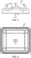
- FIG. 2illustrates a block diagram of an element array.
- FIG. 3illustrates a simplified flow diagram for testing an element array.
- FIG. 4illustrates an example of a 2-T pixel array.
- FIG. 5illustrates an example of a 3-T pixel.
- FIG. 6illustrates a cross section of a floating gate terminal transistor.
- FIG. 7illustrates a circuit schematic equivalent to a floating gate terminal transistor.
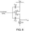
- FIG. 8illustrates a circuit schematic equivalent to a floating gate terminal transistor during a testing phase.
- Embodiments of the present inventionprovide a method of testing a chemical a chemical detecting device comprised of an array of pixel elements where each pixel element includes a chemically-sensitive transistor having a source terminal, a drain terminal, and a floating gate terminal.
- the methodmay include connecting of a group of the chemically-sensitive transistors' source terminals in common, applying first test voltages at the source terminals of the group, measuring corresponding first currents at the drain terminals produced by the first test voltages, and calculating resistance values based on the first test voltages and currents.
- the methodmay also include applying second test voltages at the source terminals of the group to operate the group in a different operational mode, wherein the second test voltages are based at least partially on the resistance values, and measuring a corresponding second set of currents at the drain terminals produced by the second test voltages. Based on the second test voltages and currents and operational properties of the chemically-sensitive transistors, calculating a floating gate voltage of each chemically-sensitive transistor in the group.
- Embodiments of the present inventionprovide a method of dry testing an array of chemically-sensitive transistors having a source, a drain, and a floating gate.
- the methodmay include applying first test voltages to a common source connected group of the chemically-sensitive transistors; calculating a resistance based on the first test voltages and currents produced by the first set of test voltages; applying second test voltages, where the second test voltages drive the chemically-sensitive transistors to transition among a plurality of operational modes and where the second test voltages are based partially on the calculated resistance; calculating a floating gate voltage of each driven chemically-sensitive transistor; and determining if each calculated floating gate voltage is within a predetermined threshold.
- Embodiments of the present inventionprovide a device including an array of chemical detection elements and a testing circuit.
- Each elementmay include a chemically-sensitive field effect transistor having a semiconductor body terminal, a source terminal, a drain terminal, and a floating gate terminal.
- the testing circuitmay include a plurality of driving voltage terminals at each side of the array where the plurality of driving voltage terminals coupled to a plurality of source terminals and a plurality of body terminals, and a current source coupled to the drain terminal of at least one element in the array to measure a drain current by converting the drain current into corresponding voltage measurements.
- Embodiments of the present inventionprovide a method of testing a transistor having a floating gate and an overlap capacitance between the floating gate and at least one of a first and a second terminal.
- the methodmay include applying a test voltage to the first terminal of the transistor, biasing a second terminal of the transistor, measuring an output voltage at the second terminal, and determining if the output voltage is within a predetermined range.
- the test voltage via the overlap capacitancemay place the transistor into an active mode.
- Embodiments of the present inventionprovide a device including an array of detection elements and a test circuit.
- Each elementmay include a field effect transistor having a floating gate, a first terminal, a second terminal, and an overlap capacitance between the floating gate and at least one of the first and second terminals.
- the testing circuitmay include a driving voltage terminal coupled to at least one first terminal, a biasing current terminal coupled to at least one second terminal, and an output voltage measurement terminal coupled to the at least one second terminal.
- Embodiments of the present inventionrelate to a system and method for testing ion-sensing devices such as an ISFET device.
- ISFETssense changes in the chemical composition in micro-wells that are formed above the ISFET. Such chemical changes may be caused by chemical reaction in fluids contained in the micro-wells.
- FIG. 1is a simplified diagram of an ISFET 100 .
- ISFET 100is illustrated as an NMOS device; however, a PMOS device may also be used in aspects of the present invention.
- the ISFET 100is a semiconductor device with four terminals. The four terminals are a gate terminal 110 , a drain terminal 120 , a source terminal 130 , and a body terminal 140 .
- the gate terminal 110may be a floating gate.
- the ISFET 100may include a floating gate with a micro-well above the floating gate.
- This micro-wellmay contain an oxide (or other materials) with surface sites that cause a specific ion species to bind, inducing a change in charge distribution, and causing a change in potential at the surface.
- This change in surface potentialmay then be detected by the ISFET and measured by a read circuit, and represents the amount of ions contained within the micro-well. It is in this way that each ISFET in an array (e.g., ISFET element array 210 of FIG. 2 ) can be used to detect local variations in ion concentration of a sample liquid that is presented over the array.
- the ISFET 100may operate similar to a standard MOSFET device and may transition among a few operational regions. When the ISFET 100 is biased such that V GS ⁇ V th is positive and greater than V DS , the transistor is in the triode region, which is also commonly referred to as the linear region. In the triode region, the current through the drain terminal 120 , I D , may be defined as:
- I D⁇ n ⁇ C ox ⁇ W L ⁇ ( ( V GS - V th ) ⁇ V DS - V DS 2 2 ) Triode ⁇ ⁇ Region ⁇ ⁇ Equation
- ⁇ n inis a charge-carrier effective mobility coefficient
- C oxis a gate oxide capacitance per unit area coefficient
- Wis a gate width
- Lis a gate length
- V GSis a voltage between the gate and source terminals
- V this the threshold voltage
- V DSis the voltage between the drain and source terminals.
- the transistorhas ohmic behavior between the drain and source and the drain current does not saturate.
- the ISFET 100When V GS ⁇ V th is positive and less than V DS , the ISFET 100 operates in the saturation region, which is also commonly referred to as the active region. In the saturation region, the current through the drain terminal 120 , I D , may be defined as:
- I D⁇ n ⁇ C ox 2 ⁇ W L ⁇ ( V GS - V th ) 2 ⁇ ( 1 + ⁇ ⁇ ⁇ V DS ) Saturation ⁇ ⁇ Region ⁇ ⁇ Equation
- ⁇ nis the charge-carrier effective mobility coefficient
- C oxis the gate oxide capacitance per unit area coefficient
- Wis the gate width
- Lis the gate length
- V GSthe voltage between the gate and source terminals
- V this the threshold voltage
- V DSis the voltage between the drain and source terminals
- ⁇ the factor for channel length modulation⁇ n ⁇ C ox 2 ⁇ W L ⁇ ( V GS - V th ) 2 ⁇ ( 1 + ⁇ ⁇ ⁇ V DS ) Saturation ⁇ ⁇ Region ⁇ ⁇ Equation
- the ISFET 100also has a threshold voltage dependent on the bulk potential.
- the bulk potentialis referred to as the body voltage at terminal 140 and may operate as a second gate.
- the ISFET 100may be placed in a pixel element, and the pixel element may be a part of an array.
- FIG. 2illustrates a device 200 with an ISFET element array 210 .
- Each element in the array 210may include an ISFET as described above in FIG. 1 and may also include other transistors and electrical components.
- the array 210may be arranged as a plurality of rows and columns.
- the array 210may also have ISFET terminal connections at both ends of the columns and both sides of the rows, and, thus, may have ISFET terminal connections at each of the four edges of the array 210 .
- the body connectionmay be set to a bias voltage.
- each edgemay have source connections of the ISFET in the array 210 as described below.
- the array 210is typically large and thus the source resistance along the array may vary by the inherent resistance of the transistor well and connection to the source.
- the ISFET array 210may be tested by strategically placing body and source connections access at different physical locations around the array. Resistance of the source connections may then be calibrated to determine an accurate representation of the desired floating gate voltage.
- FIG. 3illustrates a simplified flow diagram of a method 300 to test an ISFET array, without the presence of fluids in contact with or adjacent to the array, according to an embodiment of the present invention.
- the devicemay be entered into a test mode where the device circuitry may connect the sources of all the ISFETs in common (i.e., all of the ISFET sources are connected together) (Step 310 ).
- the array circuitrymay connect the sources of alternate rows or columns in common (e.g., the sources of odd numbered rows connected together and the sources of even numbered rows connected together).
- the alternate rows or column arrangementmay be a structural array testing technique to allow the test procedure to test the integrity of the arrays of the rows and columns.
- the presence of column defectsmay be tested by driving odd columns (but not even columns) high (e.g. by applying a voltage) and measuring the even columns to see whether the even columns stay low. If an even column measures high, this identifies a defective column.
- odd columnsbut not even columns
- structural array testingmay test the connectivity of rows and columns in the array.
- other or similar connections to drains of the ISFETsmay also be established.
- a first testmay be performed (Step 320 ).
- first test voltagesmay be forced (applied) through the array.
- the first test voltagesmay be applied at multiple sides of the device such as either end of the columns or either side of the rows in the array. For example, the first test voltages may be applied to each of the sides sequentially.
- the first test voltagesmay be applied to the body and source terminals of the connected ISFETs.
- the first test voltagesmay include an initial voltage sweep to identify a suitable operating (or bias) voltage to test the pixel array.
- First test measurements corresponding to the first testmay then be obtained (Step 330 ).
- the first test voltagesmay produce corresponding currents through each connected ISFET.
- the produced currentsmay then be measured.
- a range of different voltage and current measurementsmay be provided in the embodiments of the present invention.
- source and drain voltagesmay be forced while setting the body to a bias voltage of either an analog supply voltage or analog ground (depending on whether the ISFET is a PMOS or NMOS device).
- the resultant drain currentmay then be measured by a current source converting the measured current into a corresponding voltage value.
- the bodyin principle, may be set to a voltage between the analog supply voltage and analog ground. Further, all body terminals may be set to the same voltage in an ISFET array and, thus, all the ISFETS in the array may be similarly biased.
- Another testmay characterize threshold voltage mismatches across the array.
- a resistance value for the source connectionsmay be calculated (Step 340 ). For example, a resistance gradient for the source connections may be calculated showing the resistance relationship of the test voltages and measured currents.
- body and source connections relative to one side of the devicemay be established.
- a second testmay then be performed (Step 350 ).
- second test voltages and currentsmay be forced or applied through the array.
- the second test voltagesmay be a voltage sweep at different operating (or bias) voltage points.
- the body connectionwhich is a bias voltage, may be set accordingly.
- the second test voltages and currentsmay be a sweep of a range of voltages that will operate the ISFETs in a different operational mode as described above, such as triode mode and saturation mode. Further, the ISFETs may be operated in body effect mode by using the body terminal as a second gate.
- Second test measurements corresponding to the second testmay then be obtained (Step 360 ).
- different currents and voltages as seen on the arraymay be measured.
- source and drain voltagesmay be forced while the body voltage ranges between the analog supply voltage and analog ground voltage.
- the produced drain currentsmay be measured by a current source that may convert the current into corresponding voltage values.
- the gate voltage of the ISFETsmay be calculated (Step 370 ). Specifically, the operational equations of the different modes described above may be used to calculate the gate voltage based on the forced and measured voltages and currents. Thus, the gate voltage for each ISFET element may be calculated to determine if the ISFET is working properly.
- steps 350 - 370may be repeated for one or more other sides of the device (such as, e.g., the opposite end of the column). In another embodiment, steps 350 - 370 may be repeated after increasing or decreasing the forced voltages and currents by a factor of, for example, two. The gate voltage may then be calculated from the adjusted voltage (the bias point). The increased or decreased iteration may also be repeated for one or more other sides of the device. Also, the increasing or decreasing iteration may be repeated multiple times, each time in which the forced voltages and currents are adjusted by some factor with each iteration. After all iterations are complete, the calculated gate voltages may be averaged together to obtain a more accurate representation of the ISFET gate voltage.
- the averaged gate voltagemay then be compared to a desired threshold range to determine if each ISFET is working properly. Further, the location (e.g., X and Y column and row in the array), values for each ISFET gate voltage, and/or the working condition of each ISFET may be recorded in a register, for example. Additional circuitry may be provided to allow for programming and/or erasing of each pixel element where the floating gate voltage of each ISFET may be programmed and/or erased. In some embodiments, the program/erase capability may provide a higher level of fault detection coverage. However, the program/erase circuitry may operate on a higher voltage than other circuit components, and design techniques to isolate higher voltage circuits may need to be applied to ensure circuit components are not damaged.
- the temperature of the devicemay also be varied to modulate the threshold voltage of the ISFET element. By varying the temperature, alternate data points may be observed and used to calculate the gate voltage of the ISFET element.
- FIG. 4illustrates a two-transistor (2-T) pixel array 400 showing 4 pixel elements that may be used in aspects of the present invention.
- the pixel array 400may include a plurality of pixel elements 401 . 1 - 401 . n .
- Each pixel element 401may include an ISFET 410 and another transistor 420 .
- the arraymay be tested by controlling and/or measuring all nodes except the floating gate terminal of the ISFET.
- FIG. 5illustrates a three-transistor (3-T) pixel element 500 that may be used in aspects of the present invention.
- the pixel element 500may include an ISFET 510 , and two other transistors 520 , 530 .
- the arraymay be tested by controlling and/or measuring all nodes except the floating gate terminal of the ISFET.
- the I-Sinkmay be a controllable current source to provide a constant current to the ISFET.
- the I Sink capabilityadds another measurement point that may be used to more accurately calculate the gate voltage.
- Other variations of the pixel circuitrymay be used with the embodiments of the present invention.
- aspects of the present inventionhave been described in which an ISFET array may be tested without the use of liquids, aspects of the present invention may be employed in conjunction with the use of liquids for testing purposes.
- liquids having a known pHmay be applied before, during, or after the dry testing techniques described herein.
- dry testing techniques described hereinmay be used together with wet testing techniques, if desired.
- ISFETinductor field-effect transistor
- the present inventionis not limited to ISFETs and may be applicable to other suitable floating gate transistor devices or other suitable chemically-sensitive transistors.
- FIG. 6shows a simplified diagram of a floating gate transistor 600 such as an ISFET.
- the transistor 600may include a floating gate 612 , a drain 614 , and a source 616 .
- the drain 614 and source 616may be p-type implants within an n-type substrate, thus forming a p-channel FET device.
- the transistor 600may be formed using an n-channel FET device having its drain and source formed using n-type implants within a p-type semiconductor.
- An ISFETmay be formed, generally, using a self-aligned process.
- a polysilicon gatemay be formed, and floating gate 612 may be formed on a gate oxide 615 or other suitable gate insulator.
- Source and drain implantsmay be made in several steps. Before a nitride spacer is applied, an LDD (lightly doped drain) implant may be made. The LDD implant diffuses a small distance under the gate to reduce the electric field and to reduce the negative aspects of transistor performance such as hot carriers.
- the LDD implantalong with a step of degenerative doped implantation, forms the drain 614 and the source 616 .
- the drain 614 and source 616may have partially overlapping portions 607 , 608 arranged under respective portions of gate oxide 615 .
- the overlapping portions 607 , 608are formed within their respective implants such that a portion of the implants are beneath the floating gate electrode creating a parasitic capacitance.
- a process parameter relating to size of the overlap portionsmay be adjusted to control the size of the overlap portion and their capacitance.
- FIG. 7shows a circuit schematic equivalent to transistor 600 illustrating parasitic capacitance between the gate and source (C GS ) and parasitic capacitance between the gate and drain (C GD ).
- parasitic capacitancemay exist between the gate and drain only or between the gate and source only.
- FIG. 8illustrates a floating gate transistor test structure for a pixel element in an array according to an embodiment of the present invention.
- the floating gate transistore.g. an ISFET
- the drain of the floating gate transistormay be coupled to a voltage power supply, V DD , to drive the transistor.
- V DDmay be 3 volts.
- the source of the floating gate transistormay be biased with a current source.
- the current sourcemay be a 1 ⁇ A current source.
- the voltage at the source(shown as V OUT in FIG. 8 ) may then be measured.
- the source voltage V OUTmay be representative of the voltage on the floating gate.
- the parasitic capacitance of the transistorforces the floating gate into the saturation region and, thus, the transistor may produce source voltage V OUT , which follows the gate potential of interest.
- the transistor's threshold voltage and parasitic capacitance valuesmay be designed to allow the proper coupling to the floating gate that is sufficient to bring the transistor into its operational range.
- the pixelmay be considered operational because the test determines that the floating gate transistor can produce a valid and measurable signal. However, if the measured signal is too high or too low as compared to the normal distribution, it may indicate that an excessive trapped charge may be present at the floating gate. Also, if the distribution of the measured values in the tested array is significantly wide, it may indicate a large non-uniformity of the individual pixel elements. Large non-uniformities are generally considered unreliable and, thus, the array may be unusable.
- the floating gate transistor testmay be expanded to measure the gain of the pixel and/or to determine other pixel properties. Again, the test may be conducted without using a fluidic bias to operate the floating gate and, therefore, maintaining the integrity of the array.
- the drain voltagemay be varied while measuring corresponding source voltages.
- the source biasing currentmay held constant while the drain voltage is varied.
- a first voltagemay be applied to the drain, for example 3V, and the source may be biased accordingly.
- the drain voltagemay be adjusted to a second voltage, for example 2.8V, while the bias current at the source is held constant from the first step.
- the corresponding source voltagemay be measured.
- the difference in the drain voltage200 mV in the example
- the resulting source voltagemay thus be a fraction of the drain voltage difference.
- the ratio of the measured value to the input voltagerepresents the pixel gain and may be used to ascertain other pixel properties of interest.
- Various embodimentsmay be implemented using hardware elements, software elements, or a combination of both.
- hardware elementsmay include processors, microprocessors, circuits, circuit elements (e.g., transistors, resistors, capacitors, inductors, and so forth), integrated circuits, application specific integrated circuits (ASIC), programmable logic devices (PLD), digital signal processors (DSP), field programmable gate array (FPGA), logic gates, registers, semiconductor device, chips, microchips, chip sets, and so forth.
- Examples of softwaremay include software components, programs, applications, computer programs, application programs, system programs, machine programs, operating system software, middleware, firmware, software modules, routines, subroutines, functions, methods, procedures, software interfaces, application program interfaces (API), instruction sets, computing code, computer code, code segments, computer code segments, words, values, symbols, or any combination thereof. Determining whether an embodiment is implemented using hardware elements and/or software elements may vary in accordance with any number of factors, such as desired computational rate, power levels, heat tolerances, processing cycle budget, input data rates, output data rates, memory resources, data bus speeds and other design or performance constraints.
- Some embodimentsmay be implemented, for example, using a computer-readable medium or article which may store an instruction or a set of instructions that, if executed by a machine, may cause the machine to perform a method and/or operations in accordance with the embodiments.
- a machinemay include, for example, any suitable processing platform, computing platform, computing device, processing device, computing system, processing system, computer, processor, or the like, and may be implemented using any suitable combination of hardware and/or software.
- the computer-readable medium or articlemay include, for example, any suitable type of memory unit, memory device, memory article, memory medium, storage device, storage article, storage medium and/or storage unit, for example, memory, removable or non-removable media, erasable or non-erasable media, writeable or re-writeable media, digital or analog media, hard disk, floppy disk, Compact Disc Read Only Memory (CD-ROM), Compact Disc Recordable (CD-R), Compact Disc Rewriteable (CD-RW), optical disk, magnetic media, magneto-optical media, removable memory cards or disks, various types of Digital Versatile Disc (DVD), a tape, a cassette, or the like.
- any suitable type of memory unitfor example, any suitable type of memory unit, memory device, memory article, memory medium, storage device, storage article, storage medium and/or storage unit, for example, memory, removable or non-removable media, erasable or non-erasable media, writeable or re-writeable media, digital or analog media, hard disk
- the instructionsmay include any suitable type of code, such as source code, compiled code, interpreted code, executable code, static code, dynamic code, encrypted code, and the like, implemented using any suitable high-level, low-level, object-oriented, visual, compiled and/or interpreted programming language.
Landscapes
- Physics & Mathematics (AREA)
- Engineering & Computer Science (AREA)
- General Physics & Mathematics (AREA)
- Microelectronics & Electronic Packaging (AREA)
- Chemical & Material Sciences (AREA)
- Health & Medical Sciences (AREA)
- Life Sciences & Earth Sciences (AREA)
- Analytical Chemistry (AREA)
- Biochemistry (AREA)
- Molecular Biology (AREA)
- Electromagnetism (AREA)
- Chemical Kinetics & Catalysis (AREA)
- Electrochemistry (AREA)
- General Engineering & Computer Science (AREA)
- Computer Hardware Design (AREA)
- General Health & Medical Sciences (AREA)
- Immunology (AREA)
- Pathology (AREA)
- Thin Film Transistor (AREA)
- Investigating Or Analyzing Materials By The Use Of Electric Means (AREA)
- Testing Of Individual Semiconductor Devices (AREA)
- Insulated Gate Type Field-Effect Transistor (AREA)
Abstract
Description
where μnin is a charge-carrier effective mobility coefficient, Coxis a gate oxide capacitance per unit area coefficient, W is a gate width, L is a gate length, VGSis a voltage between the gate and source terminals, Vthis the threshold voltage, and VDSis the voltage between the drain and source terminals. In the triode region, the transistor has ohmic behavior between the drain and source and the drain current does not saturate.
where μnis the charge-carrier effective mobility coefficient, Coxis the gate oxide capacitance per unit area coefficient, W is the gate width, L is the gate length, VGSis the voltage between the gate and source terminals, Vthis the threshold voltage, VDSis the voltage between the drain and source terminals, and λ the factor for channel length modulation.
VTN=VTO+γ(√{square root over (VSB+2ϕ)}−√{square root over (2ϕ)}) Body Effect Equation
where VTNis a threshold voltage with substrate bias present, VTOis a zero-VSBvalue of threshold voltage, VSBis a voltage between the source and body terminals, γ is a body effect parameter, and 2ϕ is a surface potential parameter.
Claims (23)
Priority Applications (2)
| Application Number | Priority Date | Filing Date | Title |
|---|---|---|---|
| US15/979,439US11231451B2 (en) | 2010-06-30 | 2018-05-14 | Methods and apparatus for testing ISFET arrays |
| US17/535,367US20220082607A1 (en) | 2010-06-30 | 2021-11-24 | Methods and apparatus for testing isfet arrays |
Applications Claiming Priority (4)
| Application Number | Priority Date | Filing Date | Title |
|---|---|---|---|
| US36049310P | 2010-06-30 | 2010-06-30 | |
| US36049510P | 2010-07-01 | 2010-07-01 | |
| US13/173,621US20120001646A1 (en) | 2010-06-30 | 2011-06-30 | Methods and apparatus for testing isfet arrays |
| US15/979,439US11231451B2 (en) | 2010-06-30 | 2018-05-14 | Methods and apparatus for testing ISFET arrays |
Related Parent Applications (1)
| Application Number | Title | Priority Date | Filing Date |
|---|---|---|---|
| US13/173,621ContinuationUS20120001646A1 (en) | 2010-06-30 | 2011-06-30 | Methods and apparatus for testing isfet arrays |
Related Child Applications (1)
| Application Number | Title | Priority Date | Filing Date |
|---|---|---|---|
| US17/535,367DivisionUS20220082607A1 (en) | 2010-06-30 | 2021-11-24 | Methods and apparatus for testing isfet arrays |
Publications (2)
| Publication Number | Publication Date |
|---|---|
| US20190033363A1 US20190033363A1 (en) | 2019-01-31 |
| US11231451B2true US11231451B2 (en) | 2022-01-25 |
Family
ID=45399230
Family Applications (3)
| Application Number | Title | Priority Date | Filing Date |
|---|---|---|---|
| US13/173,621AbandonedUS20120001646A1 (en) | 2010-06-30 | 2011-06-30 | Methods and apparatus for testing isfet arrays |
| US15/979,439Active2033-10-21US11231451B2 (en) | 2010-06-30 | 2018-05-14 | Methods and apparatus for testing ISFET arrays |
| US17/535,367AbandonedUS20220082607A1 (en) | 2010-06-30 | 2021-11-24 | Methods and apparatus for testing isfet arrays |
Family Applications Before (1)
| Application Number | Title | Priority Date | Filing Date |
|---|---|---|---|
| US13/173,621AbandonedUS20120001646A1 (en) | 2010-06-30 | 2011-06-30 | Methods and apparatus for testing isfet arrays |
Family Applications After (1)
| Application Number | Title | Priority Date | Filing Date |
|---|---|---|---|
| US17/535,367AbandonedUS20220082607A1 (en) | 2010-06-30 | 2021-11-24 | Methods and apparatus for testing isfet arrays |
Country Status (6)
| Country | Link |
|---|---|
| US (3) | US20120001646A1 (en) |
| EP (1) | EP2588850B1 (en) |
| JP (2) | JP5952813B2 (en) |
| CN (2) | CN106932456B (en) |
| TW (3) | TWI539172B (en) |
| WO (1) | WO2012003359A1 (en) |
Cited By (1)
| Publication number | Priority date | Publication date | Assignee | Title |
|---|---|---|---|---|
| US11327045B2 (en)* | 2018-10-18 | 2022-05-10 | Globalfoundries Singapore Pte. Ltd. | Sensor device for detecting a pH change in a solution and a method for forming the sensor device |
Families Citing this family (53)
| Publication number | Priority date | Publication date | Assignee | Title |
|---|---|---|---|---|
| US8262900B2 (en) | 2006-12-14 | 2012-09-11 | Life Technologies Corporation | Methods and apparatus for measuring analytes using large scale FET arrays |
| US8349167B2 (en) | 2006-12-14 | 2013-01-08 | Life Technologies Corporation | Methods and apparatus for detecting molecular interactions using FET arrays |
| CA2672315A1 (en) | 2006-12-14 | 2008-06-26 | Ion Torrent Systems Incorporated | Methods and apparatus for measuring analytes using large scale fet arrays |
| US11339430B2 (en) | 2007-07-10 | 2022-05-24 | Life Technologies Corporation | Methods and apparatus for measuring analytes using large scale FET arrays |
| CN102203282B (en) | 2008-06-25 | 2014-04-30 | 生命技术公司 | Methods and apparatus for measuring analytes using large scale FET arrays |
| US20100301398A1 (en) | 2009-05-29 | 2010-12-02 | Ion Torrent Systems Incorporated | Methods and apparatus for measuring analytes |
| US20100137143A1 (en) | 2008-10-22 | 2010-06-03 | Ion Torrent Systems Incorporated | Methods and apparatus for measuring analytes |
| US8776573B2 (en) | 2009-05-29 | 2014-07-15 | Life Technologies Corporation | Methods and apparatus for measuring analytes |
| US20120261274A1 (en) | 2009-05-29 | 2012-10-18 | Life Technologies Corporation | Methods and apparatus for measuring analytes |
| US8673627B2 (en) | 2009-05-29 | 2014-03-18 | Life Technologies Corporation | Apparatus and methods for performing electrochemical reactions |
| WO2012003363A1 (en) | 2010-06-30 | 2012-01-05 | Life Technologies Corporation | Ion-sensing charge-accumulation circuits and methods |
| TWI539172B (en) | 2010-06-30 | 2016-06-21 | 生命技術公司 | Methods and apparatus for testing isfet arrays |
| JP2013540259A (en) | 2010-06-30 | 2013-10-31 | ライフ テクノロジーズ コーポレーション | Array column integrator |
| US11307166B2 (en) | 2010-07-01 | 2022-04-19 | Life Technologies Corporation | Column ADC |
| EP2589065B1 (en)* | 2010-07-03 | 2015-08-19 | Life Technologies Corporation | Chemically sensitive sensor with lightly doped drains |
| WO2012036679A1 (en) | 2010-09-15 | 2012-03-22 | Life Technologies Corporation | Methods and apparatus for measuring analytes |
| US8796036B2 (en) | 2010-09-24 | 2014-08-05 | Life Technologies Corporation | Method and system for delta double sampling |
| US9689835B2 (en) | 2011-10-31 | 2017-06-27 | Taiwan Semiconductor Manufacturing Company, Ltd. | Amplified dual-gate bio field effect transistor |
| US9459234B2 (en) | 2011-10-31 | 2016-10-04 | Taiwan Semiconductor Manufacturing Company, Ltd., (“TSMC”) | CMOS compatible BioFET |
| US9970984B2 (en) | 2011-12-01 | 2018-05-15 | Life Technologies Corporation | Method and apparatus for identifying defects in a chemical sensor array |
| US8747748B2 (en) | 2012-01-19 | 2014-06-10 | Life Technologies Corporation | Chemical sensor with conductive cup-shaped sensor surface |
| US8821798B2 (en) | 2012-01-19 | 2014-09-02 | Life Technologies Corporation | Titanium nitride as sensing layer for microwell structure |
| TWI601260B (en)* | 2012-04-13 | 2017-10-01 | 聯華電子股份有限公司 | Test structure for semiconductor process and method for monitoring semiconductor process |
| US9070652B2 (en)* | 2012-04-13 | 2015-06-30 | United Microelectronics Corp. | Test structure for semiconductor process and method for monitoring semiconductor process |
| US8786331B2 (en) | 2012-05-29 | 2014-07-22 | Life Technologies Corporation | System for reducing noise in a chemical sensor array |
| DE102012213530A1 (en)* | 2012-08-01 | 2014-02-06 | Robert Bosch Gmbh | A method and apparatus for determining a state of a semiconductor material of a chemosensitive field effect transistor tested and supplied by a manufacturer |
| DE102012213533A1 (en)* | 2012-08-01 | 2014-02-06 | Robert Bosch Gmbh | A semiconductor device and method for determining a state of a semiconductor material of the semiconductor device |
| US9599586B2 (en)* | 2012-08-27 | 2017-03-21 | Infineon Technologies Ag | Ion sensor |
| US9080968B2 (en) | 2013-01-04 | 2015-07-14 | Life Technologies Corporation | Methods and systems for point of use removal of sacrificial material |
| US9841398B2 (en) | 2013-01-08 | 2017-12-12 | Life Technologies Corporation | Methods for manufacturing well structures for low-noise chemical sensors |
| US8962366B2 (en) | 2013-01-28 | 2015-02-24 | Life Technologies Corporation | Self-aligned well structures for low-noise chemical sensors |
| US8963216B2 (en) | 2013-03-13 | 2015-02-24 | Life Technologies Corporation | Chemical sensor with sidewall spacer sensor surface |
| US8841217B1 (en) | 2013-03-13 | 2014-09-23 | Life Technologies Corporation | Chemical sensor with protruded sensor surface |
| US9389199B2 (en) | 2013-03-14 | 2016-07-12 | Taiwan Semiconductor Manufacturing Company, Ltd. | Backside sensing bioFET with enhanced performance |
| US20140264468A1 (en) | 2013-03-14 | 2014-09-18 | Taiwan Semiconductor Manufacturing Company, Ltd. | Biofet with increased sensing area |
| US9116117B2 (en) | 2013-03-15 | 2015-08-25 | Life Technologies Corporation | Chemical sensor with sidewall sensor surface |
| EP2972280B1 (en) | 2013-03-15 | 2021-09-29 | Life Technologies Corporation | Chemical sensor with consistent sensor surface areas |
| EP2972279B1 (en) | 2013-03-15 | 2021-10-06 | Life Technologies Corporation | Chemical sensors with consistent sensor surface areas |
| US9835585B2 (en) | 2013-03-15 | 2017-12-05 | Life Technologies Corporation | Chemical sensor with protruded sensor surface |
| JP6671274B2 (en) | 2013-03-15 | 2020-03-25 | ライフ テクノロジーズ コーポレーション | Chemical device with thin conductive element |
| US20140336063A1 (en) | 2013-05-09 | 2014-11-13 | Life Technologies Corporation | Windowed Sequencing |
| US10458942B2 (en) | 2013-06-10 | 2019-10-29 | Life Technologies Corporation | Chemical sensor array having multiple sensors per well |
| CN107407656B (en)* | 2014-12-18 | 2020-04-07 | 生命科技公司 | Method and apparatus for measuring analytes using large scale FET arrays |
| KR102593647B1 (en) | 2014-12-18 | 2023-10-26 | 라이프 테크놀로지스 코포레이션 | High data rate integrated circuit with transmitter configuration |
| US10077472B2 (en) | 2014-12-18 | 2018-09-18 | Life Technologies Corporation | High data rate integrated circuit with power management |
| BR112017024043B1 (en)* | 2015-05-08 | 2022-05-24 | The Climate Corporation | Portable ion concentration device and ground monitoring device |
| JP6239665B2 (en)* | 2016-03-16 | 2017-11-29 | 株式会社東芝 | Semiconductor device |
| ES3037403T3 (en) | 2018-09-21 | 2025-10-01 | Teralytic Holdings Inc | Extensible, multimodal sensor fusion platform for remote, proximal soil sensing |
| US11483686B2 (en)* | 2018-11-19 | 2022-10-25 | ENGEO Incorporated | System and methods for remote interaction with portable field measurement equipment |
| CN111341799A (en)* | 2018-12-18 | 2020-06-26 | 群创光电股份有限公司 | Electronic device and manufacturing process thereof |
| TWI694447B (en)* | 2019-08-23 | 2020-05-21 | 卡比科技有限公司 | Non-volatile memory |
| CN115184436B (en)* | 2022-07-29 | 2025-01-17 | 上海天马微电子有限公司 | Detection device and detection method thereof |
| CN115825568B (en)* | 2022-11-02 | 2025-08-29 | 长鑫存储技术有限公司 | Test method, test circuit, controller, and semiconductor memory |
Citations (447)
| Publication number | Priority date | Publication date | Assignee | Title |
|---|---|---|---|---|
| US4086642A (en) | 1975-01-16 | 1978-04-25 | Hitachi, Ltd. | Protective circuit and device for metal-oxide-semiconductor field effect transistor and method for fabricating the device |
| JPS5870155A (en) | 1981-07-24 | 1983-04-26 | フオンダシヨン・スイス・プ−ル・ラ・レシエルシユ・アン・ミクロテクニク | Semiconductor device responding to ion |
| US4411741A (en) | 1982-01-12 | 1983-10-25 | University Of Utah | Apparatus and method for measuring the concentration of components in fluids |
| US4438354A (en) | 1981-08-14 | 1984-03-20 | American Microsystems, Incorporated | Monolithic programmable gain-integrator stage |
| US4437969A (en) | 1981-04-09 | 1984-03-20 | Corning Glass Works | Offset-gate chemical-sensitive field-effect transistors (OG-CHEMFETS) with electrolytically-programmable selectivity |
| US4444644A (en) | 1981-02-17 | 1984-04-24 | Sumitomo Electric Industries, Ltd. | PH Electrode |
| US4490678A (en) | 1981-05-15 | 1984-12-25 | Licentia Patent-Verwaltungs-G.M.B.H. | Method of and an apparatus for measuring ion concentrations in solutions |
| US4641084A (en) | 1983-12-15 | 1987-02-03 | Olympus Optical Co., Ltd. | Ion concentration measuring apparatus |
| US4660063A (en) | 1985-03-18 | 1987-04-21 | General Electric Company | Immersion type ISFET |
| US4691167A (en) | 1983-08-24 | 1987-09-01 | Sentron V.O.F. | Apparatus for determining the activity of an ion (pIon) in a liquid |
| JPS62237349A (en) | 1986-04-08 | 1987-10-17 | Nec Corp | Instrument for measuring distribution of hydrogen ion concentration |
| US4722830A (en) | 1986-05-05 | 1988-02-02 | General Electric Company | Automated multiple stream analysis system |
| US4743954A (en) | 1985-06-07 | 1988-05-10 | University Of Utah | Integrated circuit for a chemical-selective sensor with voltage output |
| US4764797A (en) | 1985-09-14 | 1988-08-16 | Thorn Emi Plc | Chemical-sensitive semiconductor device |
| US4777019A (en) | 1985-04-12 | 1988-10-11 | Thomas Dandekar | Biosensor |
| US4822566A (en) | 1985-11-19 | 1989-04-18 | The Johns Hopkins University | Optimized capacitive sensor for chemical analysis and measurement |
| US4864229A (en) | 1986-05-03 | 1989-09-05 | Integrated Ionics, Inc. | Method and apparatus for testing chemical and ionic sensors |
| US4863849A (en) | 1985-07-18 | 1989-09-05 | New York Medical College | Automatable process for sequencing nucleotide |
| WO1989009283A1 (en) | 1988-03-25 | 1989-10-05 | Edward David Hyman | Pyrophosphate-based method and apparatus for sequencing nucleic acids |
| US4874499A (en) | 1988-05-23 | 1989-10-17 | Massachusetts Institute Of Technology | Electrochemical microsensors and method of making such sensors |
| US4893088A (en) | 1988-11-16 | 1990-01-09 | Harris Corporation | Transimpedance focal plane processor |
| US4927736A (en) | 1987-07-21 | 1990-05-22 | Hoechst Celanese Corporation | Hydroxy polyimides and high temperature positive photoresists therefrom |
| WO1990005910A1 (en) | 1988-11-14 | 1990-05-31 | I Stat Corp | Wholly microfabricated biosensors and process for the manufacture and use thereof |
| JPH02250331A (en) | 1989-03-24 | 1990-10-08 | Hitachi Ltd | Semiconductor device and its manufacture |
| JPH02310931A (en) | 1989-05-25 | 1990-12-26 | Mitsubishi Electric Corp | Semiconductor device and its manufacturing method |
| US5038192A (en) | 1989-04-28 | 1991-08-06 | International Business Machines Corporation | Gate array cell having FETs of different and optimized sizes |
| US5110441A (en) | 1989-12-14 | 1992-05-05 | Monsanto Company | Solid state ph sensor |
| US5126759A (en) | 1990-06-26 | 1992-06-30 | Eastman Kodak Company | Non-impact printer with token bit control of data and current regulation signals |
| US5138251A (en) | 1989-10-04 | 1992-08-11 | Olympus Optical Co., Ltd. | Fet sensor apparatus of flow-cell adaptive type and method of manufacturing the same |
| US5140393A (en) | 1985-10-08 | 1992-08-18 | Sharp Kabushiki Kaisha | Sensor device |
| US5142236A (en) | 1989-10-16 | 1992-08-25 | Marelli Autronica Spa | Switched-capacitor circuit having a full-wave-rectifying and integrating function |
| US5151587A (en) | 1990-01-10 | 1992-09-29 | Seiko Instruments Inc. | Image sensor having an array of operative and dummy bipolar transistors and pairs of pixel selecting switches connected thereto |
| US5151759A (en) | 1989-03-02 | 1992-09-29 | Thunderbird Technologies, Inc. | Fermi threshold silicon-on-insulator field effect transistor |
| US5164319A (en) | 1985-08-22 | 1992-11-17 | Molecular Devices Corporation | Multiple chemically modulated capacitance determination |
| JPH0580115A (en) | 1991-09-19 | 1993-04-02 | Fujitsu Ltd | Nonvolatile random access memory device and method of detecting floating gate voltage level in nonvolatile random access memory device |
| US5202576A (en) | 1990-08-29 | 1993-04-13 | Texas Instruments Incorporated | Asymmetrical non-volatile memory cell, arrays and methods for fabricating same |
| US5284566A (en) | 1993-01-04 | 1994-02-08 | Bacharach, Inc. | Electrochemical gas sensor with wraparound reference electrode |
| DE4232532A1 (en) | 1992-09-29 | 1994-04-28 | Ct Fuer Intelligente Sensorik | Ion-sensitive field effect transistor mfr. for higher reliability - involves electrostatic protection by diodes within well and substrate of CMOS structure in conjunction with pseudo-reference electrode |
| US5317407A (en) | 1991-03-11 | 1994-05-31 | General Electric Company | Fixed-pattern noise correction circuitry for solid-state imager |
| US5319226A (en) | 1991-09-06 | 1994-06-07 | Dong Jin Kim | Method of fabricating an ion sensitive field effect transistor with a Ta2 O5 hydrogen ion sensing membrane |
| US5407854A (en) | 1994-01-19 | 1995-04-18 | General Signal Corporation | ESD protection of ISFET sensors |
| US5436149A (en) | 1993-02-19 | 1995-07-25 | Barnes; Wayne M. | Thermostable DNA polymerase with enhanced thermostability and enhanced length and efficiency of primer extension |
| US5439839A (en) | 1994-07-13 | 1995-08-08 | Winbond Electronics Corporation | Self-aligned source/drain MOS process |
| DE4430811C1 (en) | 1994-08-30 | 1995-09-07 | Fraunhofer Ges Forschung | Ion-sensitive FET prodn., useful for mfg. integrated liq. sensor circuit |
| US5466348A (en) | 1991-10-21 | 1995-11-14 | Holm-Kennedy; James W. | Methods and devices for enhanced biochemical sensing |
| US5475337A (en) | 1992-07-24 | 1995-12-12 | Nec Corporation | Switched capacitor amplifier circuit |
| US5490971A (en) | 1994-10-25 | 1996-02-13 | Sippican, Inc. | Chemical detector |
| US5587894A (en) | 1994-03-28 | 1996-12-24 | Matsushita Electric Works, Ltd. | Power source device |
| US5593838A (en) | 1994-11-10 | 1997-01-14 | David Sarnoff Research Center, Inc. | Partitioned microelectronic device array |
| US5600451A (en) | 1993-08-12 | 1997-02-04 | Sony Corporation | Charge transfer device and output circuit thereof |
| US5627403A (en) | 1993-05-31 | 1997-05-06 | Sgs-Thomson Microelectronics S.R.L. | Adhesion between dielectric layers in an integrated circuit |
| US5631704A (en) | 1994-10-14 | 1997-05-20 | Lucent Technologies, Inc. | Active pixel sensor and imaging system having differential mode |
| US5637469A (en) | 1992-05-01 | 1997-06-10 | Trustees Of The University Of Pennsylvania | Methods and apparatus for the detection of an analyte utilizing mesoscale flow systems |
| US5646558A (en) | 1995-09-27 | 1997-07-08 | Intel Corporation | Plurality of distinct multiplexers that operate as a single multiplexer |
| US5702964A (en) | 1995-10-17 | 1997-12-30 | Lg Semicon, Co., Ltd. | Method for forming a semiconductor device having a floating gate |
| WO1998013523A1 (en) | 1996-09-27 | 1998-04-02 | Pyrosequencing Ab | Method of sequencing dna |
| US5793230A (en) | 1997-02-26 | 1998-08-11 | Sandia Corporation | Sensor readout detector circuit |
| US5846708A (en) | 1991-11-19 | 1998-12-08 | Massachusetts Institiute Of Technology | Optical and electrical methods and apparatus for molecule detection |
| US5894284A (en) | 1996-12-02 | 1999-04-13 | Motorola, Inc. | Common-mode output sensing circuit |
| US5907765A (en) | 1995-06-30 | 1999-05-25 | Motorola, Inc. | Method for forming a semiconductor sensor device |
| US5911873A (en) | 1997-05-02 | 1999-06-15 | Rosemount Analytical Inc. | Apparatus and method for operating an ISFET at multiple drain currents and gate-source voltages allowing for diagnostics and control of isopotential points |
| US5912560A (en) | 1997-02-25 | 1999-06-15 | Waferscale Integration Inc. | Charge pump circuit for voltage boosting in integrated semiconductor circuits |
| US5923421A (en) | 1997-07-24 | 1999-07-13 | Lockheed Martin Energy Research Corporation | Chemical detection using calorimetric spectroscopy |
| US5922591A (en) | 1995-06-29 | 1999-07-13 | Affymetrix, Inc. | Integrated nucleic acid diagnostic device |
| US5944970A (en) | 1997-04-29 | 1999-08-31 | Honeywell Inc. | Solid state electrochemical sensors |
| US5958703A (en) | 1996-12-03 | 1999-09-28 | Glaxo Group Limited | Use of modified tethers in screening compound libraries |
| US5965452A (en) | 1996-07-09 | 1999-10-12 | Nanogen, Inc. | Multiplexed active biologic array |
| US6021172A (en) | 1994-01-28 | 2000-02-01 | California Institute Of Technology | Active pixel sensor having intra-pixel charge transfer with analog-to-digital converter |
| JP2000055874A (en) | 1998-08-03 | 2000-02-25 | Horiba Ltd | Isfet array |
| US6107032A (en) | 1996-12-20 | 2000-08-22 | Roche Diagnostics Gmbh | Method for the direct, exponential amplification and sequencing of DNA molecules and its application |
| US6191444B1 (en) | 1998-09-03 | 2001-02-20 | Micron Technology, Inc. | Mini flash process and circuit |
| US6195585B1 (en) | 1998-06-26 | 2001-02-27 | Advanced Bionics Corporation | Remote monitoring of implantable cochlear stimulator |
| US6255678B1 (en) | 1997-05-29 | 2001-07-03 | Horiba, Ltd. | Apparatus for measuring physical and chemical phenomena |
| US20010007418A1 (en) | 1999-12-14 | 2001-07-12 | Matsushita Electric Industrial Co., Ltd. | Common mode bias generator |
| US6274320B1 (en) | 1999-09-16 | 2001-08-14 | Curagen Corporation | Method of sequencing a nucleic acid |
| US6275061B1 (en) | 1998-09-25 | 2001-08-14 | Kabushiki Kaisha Toshiba | Testing method for a substrate of active matrix display panel |
| US6280586B1 (en) | 1995-04-04 | 2001-08-28 | Micronas Gmbh | Measuring device using biological cells or chemical biologically active substances contained in an analyte |
| US6294133B1 (en) | 1998-01-14 | 2001-09-25 | Horiba, Ltd. | Multiple detecting apparatus for physical phenomenon and/or chemical phenomenon |
| US6327410B1 (en) | 1997-03-14 | 2001-12-04 | The Trustees Of Tufts College | Target analyte sensors utilizing Microspheres |
| US6353324B1 (en) | 1998-11-06 | 2002-03-05 | Bridge Semiconductor Corporation | Electronic circuit |
| US6355431B1 (en) | 1999-04-20 | 2002-03-12 | Illumina, Inc. | Detection of nucleic acid amplification reactions using bead arrays |
| US6361671B1 (en) | 1999-01-11 | 2002-03-26 | The Regents Of The University Of California | Microfabricated capillary electrophoresis chip and method for simultaneously detecting multiple redox labels |
| US20020042388A1 (en) | 2001-05-01 | 2002-04-11 | Cooper Mark J. | Lyophilizable and enhanced compacted nucleic acids |
| US6372291B1 (en) | 1999-12-23 | 2002-04-16 | Applied Materials, Inc. | In situ deposition and integration of silicon nitride in a high density plasma reactor |
| US6376256B1 (en) | 1996-08-21 | 2002-04-23 | Smithkline Beecham Corporation | Rapid process for arraying and synthesizing bead-based combinatorial libraries |
| US6403957B1 (en) | 1989-06-07 | 2002-06-11 | Affymetrix, Inc. | Nucleic acid reading and analysis system |
| US6406848B1 (en) | 1997-05-23 | 2002-06-18 | Lynx Therapeutics, Inc. | Planar arrays of microparticle-bound polynucleotides |
| US20020081714A1 (en) | 2000-05-05 | 2002-06-27 | Maneesh Jain | Devices and methods to form a randomly ordered array of magnetic beads and uses thereof |
| US6413792B1 (en) | 2000-04-24 | 2002-07-02 | Eagle Research Development, Llc | Ultra-fast nucleic acid sequencing device and a method for making and using the same |
| US20020085136A1 (en) | 2000-12-29 | 2002-07-04 | Hong-Man Moon | Array substrate for IPS mode liquid crystal display device |
| US6429027B1 (en) | 1998-12-28 | 2002-08-06 | Illumina, Inc. | Composite arrays utilizing microspheres |
| JP2002221510A (en) | 2001-01-26 | 2002-08-09 | Japan Science & Technology Corp | Storage type chemical / physical phenomenon detection device |
| US6432360B1 (en) | 1997-10-10 | 2002-08-13 | President And Fellows Of Harvard College | Replica amplification of nucleic acid arrays |
| US20020117694A1 (en) | 2000-12-22 | 2002-08-29 | Seiko Epson Corporation | Sensor cell |
| US20020117659A1 (en) | 2000-12-11 | 2002-08-29 | Lieber Charles M. | Nanosensors |
| JP2002272463A (en) | 2001-03-22 | 2002-09-24 | Olympus Optical Co Ltd | Method for judging form of monobasic polymorphism |
| EP1243925A2 (en) | 2001-03-21 | 2002-09-25 | Olympus Optical Co., Ltd. | Biochemical examination method |
| US6459398B1 (en) | 1999-07-20 | 2002-10-01 | D.S.P.C. Technologies Ltd. | Pulse modulated digital to analog converter (DAC) |
| US6465178B2 (en) | 1997-09-30 | 2002-10-15 | Surmodics, Inc. | Target molecule attachment to surfaces |
| US20020150909A1 (en) | 1999-02-09 | 2002-10-17 | Stuelpnagel John R. | Automated information processing in randomly ordered arrays |
| US6475728B1 (en) | 1997-06-11 | 2002-11-05 | Ecole Centrale De Lyon | Method for identifying and/or analyzing biological substances, present in a conductive liquid, device and affinity sensor used for implementing said method |
| US20020168678A1 (en) | 2000-06-07 | 2002-11-14 | Li-Cor, Inc. | Flowcell system for nucleic acid sequencing |
| US6482639B2 (en) | 2000-06-23 | 2002-11-19 | The United States Of America As Represented By The Secretary Of The Navy | Microelectronic device and method for label-free detection and quantification of biological and chemical molecules |
| US20020172963A1 (en) | 2001-01-10 | 2002-11-21 | Kelley Shana O. | DNA-bridged carbon nanotube arrays |
| US6485944B1 (en) | 1997-10-10 | 2002-11-26 | President And Fellows Of Harvard College | Replica amplification of nucleic acid arrays |
| US6490220B1 (en) | 2001-08-13 | 2002-12-03 | Micron Technology, Inc. | Method for reliably shutting off oscillator pulses to a charge-pump |
| US6499499B2 (en) | 2001-04-20 | 2002-12-31 | Nanostream, Inc. | Flow control in multi-stream microfluidic devices |
| US6511803B1 (en) | 1997-10-10 | 2003-01-28 | President And Fellows Of Harvard College | Replica amplification of nucleic acid arrays |
| US20030020334A1 (en) | 2001-07-19 | 2003-01-30 | Nisshinbo Industries, Inc. | Capacitor unit with electric double layer capacitors, control method and control apparatus for the same, and accumulator system for motor vehicles |
| US6518024B2 (en) | 1999-12-13 | 2003-02-11 | Motorola, Inc. | Electrochemical detection of single base extension |
| US6518146B1 (en) | 2002-01-09 | 2003-02-11 | Motorola, Inc. | Semiconductor device structure and method for forming |
| US20030032052A1 (en) | 1999-08-02 | 2003-02-13 | Molecular Dynamics, Inc. | Methods and apparatus for template capture and normalization for submicroliter reaction |
| US20030044833A1 (en) | 2001-09-06 | 2003-03-06 | Randox Laboratories Ltd. | Biomolecule array |
| US6535824B1 (en) | 1998-12-11 | 2003-03-18 | Symyx Technologies, Inc. | Sensor array-based system and method for rapid materials characterization |
| US20030054396A1 (en) | 2001-09-07 | 2003-03-20 | Weiner Michael P. | Enzymatic light amplification |
| US6537881B1 (en) | 2000-10-16 | 2003-03-25 | Advanced Micro Devices, Inc. | Process for fabricating a non-volatile memory device |
| US6538593B2 (en) | 1997-10-30 | 2003-03-25 | The Board Of Trustees Of The Leland Stanford Junior University | Method and apparatus for converting a low dynamic range analog signal to a large dynamic range floating-point digital representation |
| US20030064366A1 (en) | 2000-07-07 | 2003-04-03 | Susan Hardin | Real-time sequence determination |
| US20030068629A1 (en) | 2001-03-21 | 2003-04-10 | Rothberg Jonathan M. | Apparatus and method for sequencing a nucleic acid |
| US6571189B2 (en) | 2001-05-14 | 2003-05-27 | Hewlett-Packard Company | System and method for scanner calibration |
| US20030108867A1 (en) | 1999-04-20 | 2003-06-12 | Chee Mark S | Nucleic acid sequencing using microsphere arrays |
| US20030119020A1 (en) | 2001-07-17 | 2003-06-26 | Stevens Priscilla Wilkins | Solid-phase reactions |
| US20030124599A1 (en) | 2001-11-14 | 2003-07-03 | Shiping Chen | Biochemical analysis system with combinatorial chemistry applications |
| US20030124572A1 (en) | 2001-07-30 | 2003-07-03 | Favor Of Meso Scale Technologies, Llc. | Assay electrode having immobilized lipid/protein layers, methods of making the same and methods of using the same for luminescence test measurements |
| US20030141929A1 (en) | 2002-01-31 | 2003-07-31 | Intel Corporation | Differential amplifier offset adjustment |
| US20030141928A1 (en) | 2002-01-26 | 2003-07-31 | Samsung Electronics Co., Ltd. | Power amplifier clipping circuit for minimizing output distortion |
| US6602702B1 (en) | 1999-07-16 | 2003-08-05 | The University Of Texas System | Detection system based on an analyte reactive particle |
| US6605428B2 (en) | 1996-12-20 | 2003-08-12 | Roche Diagnostics Gmbh | Method for the direct, exponential amplification and sequencing of DNA molecules and its application |
| US20030152994A1 (en) | 1996-04-03 | 2003-08-14 | Applera Corporation | Device and method for multiple analyte detection |
| US20030155942A1 (en) | 2000-03-30 | 2003-08-21 | Roland Thewes | Sensor array and method for detecting the condition of a transistor in a sensor array |
| US6613513B1 (en) | 1999-02-23 | 2003-09-02 | Caliper Technologies Corp. | Sequencing by incorporation |
| WO2003073088A2 (en) | 2001-03-09 | 2003-09-04 | Christofer Toumazou | Apparatus and method for the detection of localised fluctuactions of ionic charge by ion sensitive field effect transistors during a chemical reaction |
| US6618083B1 (en) | 1997-12-31 | 2003-09-09 | Texas Instruments Incorporated | Mismatch-independent reset sensing for CMOS area array sensors |
| US20030175990A1 (en) | 2002-03-14 | 2003-09-18 | Hayenga Jon W. | Microfluidic channel network device |
| US6624637B1 (en) | 1998-12-16 | 2003-09-23 | Endress + Hauser Conducta Gesellschaft für Mess - und Regeltechnik mbH + Co. | Device for measuring the concentrations in a measuring liquid |
| US6627154B1 (en) | 1998-04-09 | 2003-09-30 | Cyrano Sciences Inc. | Electronic techniques for analyte detection |
| US20030186262A1 (en) | 2000-03-01 | 2003-10-02 | Fabrice Cailloux | Novel dna chips |
| JP2003279532A (en) | 2002-03-22 | 2003-10-02 | Horiba Ltd | Chemical concentration sensor and method for measuring the same |
| US20030194740A1 (en) | 1998-12-14 | 2003-10-16 | Li-Cor, Inc. | System and method for nucleic acid sequencing by polymerase synthesis |
| WO2003092325A1 (en) | 2002-04-26 | 2003-11-06 | Tayca Corporation | Composite piezoelectric vibrator |
| US20030211502A1 (en) | 2000-04-24 | 2003-11-13 | Sauer Jon R. | Ultra-fast nucleic acid sequencing device and a method for making and using the same |
| JP2003322633A (en) | 2002-05-01 | 2003-11-14 | Seiko Epson Corp | Sensor cell, biosensor, and manufacturing method thereof |
| US20030215791A1 (en) | 2002-05-20 | 2003-11-20 | Applied Spectral Imaging Ltd. | Method of and system for multiplexed analysis by spectral imaging |
| US20030215857A1 (en) | 1996-12-20 | 2003-11-20 | Roche Diagnostics Gmbh | Method for the direct, exponential amplification and sequencing of DNA molecules and its application |
| US6654505B2 (en) | 1994-10-13 | 2003-11-25 | Lynx Therapeutics, Inc. | System and apparatus for sequential processing of analytes |
| US20030224419A1 (en) | 1997-05-23 | 2003-12-04 | Lynx Therapeutics, Inc. | Data analysis and display system for ligation-based DNA sequencing |
| EP1371974A1 (en) | 2001-02-14 | 2003-12-17 | Akihiko Tanioka | Apparatus for detecting interaction between biopolymer and ligand and method thereof |
| US6671341B1 (en) | 1999-09-17 | 2003-12-30 | Agere Systems, Inc. | Glitch-free phase switching synthesizer |
| US20040002470A1 (en) | 2000-04-13 | 2004-01-01 | Tim Keith | Novel human gene relating to respiratory diseases, obesity, and inflammatory bowel disease |
| US6682899B2 (en) | 1996-12-12 | 2004-01-27 | Prolume, Ltd. | Apparatus and method for detecting and identifying infectious agents |
| US6686638B2 (en) | 2000-12-23 | 2004-02-03 | Robert Bosch Gmbh | Micromechanical component including function components suspended movably above a substrate |
| US20040023253A1 (en) | 2001-06-11 | 2004-02-05 | Sandeep Kunwar | Device structure for closely spaced electrodes |
| WO2004017068A1 (en) | 2002-08-12 | 2004-02-26 | Hitachi High-Technologies Corporation | Method of detecting nucleic acid by using dna microarrays and nucleic acid detection apparatus |
| US6700814B1 (en) | 2002-10-30 | 2004-03-02 | Motorola, Inc. | Sense amplifier bias circuit for a memory having at least two distinct resistance states |
| US6703660B2 (en) | 1999-02-22 | 2004-03-09 | Yissum Research Development Company Of The Hebrew University Of Jerusalem | Hybrid electrical device with biological components |
| US20040049237A1 (en) | 2002-07-12 | 2004-03-11 | Larson Dennis E. | Minute ventilation sensor with dynamically adjusted excitation current |
| US6716629B2 (en) | 2000-10-10 | 2004-04-06 | Biotrove, Inc. | Apparatus for assay, synthesis and storage, and methods of manufacture, use, and manipulation thereof |
| US20040079636A1 (en) | 2002-10-25 | 2004-04-29 | Chin Hsia | Biomedical ion sensitive semiconductor sensor and sensor array |
| WO2004040291A1 (en) | 2002-10-29 | 2004-05-13 | Cornell Research Foundation, Inc. | Chemical-sensitive floating gate field effect transistor |
| US20040106211A1 (en) | 2000-02-18 | 2004-06-03 | Trustees Of Tufts College | Intelligent electro-optical sensor array and method for analyte detection |
| WO2004048962A1 (en) | 2002-11-28 | 2004-06-10 | Christian Schneider | Integrated electronic circuit comprising field effect sensors for detecting biomolecules |
| US20040121354A1 (en) | 2002-09-06 | 2004-06-24 | Hitachi Ltd. | System and method for detecting biological and chemical material |
| US20040130377A1 (en) | 2002-11-26 | 2004-07-08 | Akira Takeda | Switched capacitor amplifier circuit and electronic device |
| US6762022B2 (en) | 1997-03-05 | 2004-07-13 | The Regents Of The University Of Michigan | Compositions and methods for analysis of nucleic acids |
| US20040136866A1 (en) | 2002-06-27 | 2004-07-15 | Nanosys, Inc. | Planar nanowire based sensor elements, devices, systems and methods for using and making same |
| US20040146849A1 (en) | 2002-01-24 | 2004-07-29 | Mingxian Huang | Biochips including ion transport detecting structures and methods of use |
| US6770472B2 (en) | 2000-11-17 | 2004-08-03 | The Board Of Trustees Of The Leland Stanford Junior University | Direct DNA sequencing with a transcription protein and a nanometer scale electrometer |
| US6780591B2 (en) | 1998-05-01 | 2004-08-24 | Arizona Board Of Regents | Method of determining the nucleotide sequence of oligonucleotides and DNA molecules |
| US6795006B1 (en) | 2003-07-18 | 2004-09-21 | Zarlink Semiconductor Ab | Integrator reset mechanism |
| WO2004081234A2 (en) | 2003-03-10 | 2004-09-23 | Casio Computer Co., Ltd. | Dna analyzing apparatus, dna sensor, and analyzing method |
| US20040185591A1 (en) | 2003-03-19 | 2004-09-23 | Hsiung Stephen S.K. | Method for fabricating a titanium nitride sensing membrane on an EGFET |
| US20040185484A1 (en) | 2003-01-29 | 2004-09-23 | Costa Gina L. | Method for preparing single-stranded DNA libraries |
| US20040197803A1 (en) | 2002-12-06 | 2004-10-07 | Hidenobu Yaku | Method, primer and kit for determining base type |
| US20040207384A1 (en) | 2001-07-10 | 2004-10-21 | Infineon Technologies Ag | Measuring cell and measuring field comprising measuring cells of this type, use of a measuring and use of a measuring field |
| US6828100B1 (en) | 1999-01-22 | 2004-12-07 | Biotage Ab | Method of DNA sequencing |
| US6841128B2 (en) | 2000-03-17 | 2005-01-11 | Hitachi, Ltd. | DNA base sequencing system |
| US20050006234A1 (en) | 2003-02-13 | 2005-01-13 | Arjang Hassibi | Semiconductor electrochemical bio-sensor array |
| US20050009022A1 (en) | 2001-07-06 | 2005-01-13 | Weiner Michael P. | Method for isolation of independent, parallel chemical micro-reactions using a porous filter |
| US20050031490A1 (en) | 2001-03-09 | 2005-02-10 | Walter Gumbrecht | Module for an analysis device, applicator as an exchange part of the analysis device and analysis device associated therewith |
| US20050032075A1 (en) | 2002-10-01 | 2005-02-10 | Hidenobu Yaku | Method of detecting primer extension reaction, method of discriminating base type, device for discriminating base type, device for detecting pyrophosphate, method of detecting nucleic acid and tip for introducing sample solution |
| CN1582334A (en) | 2001-12-19 | 2005-02-16 | 株式会社日立高新技术 | Potentionmetric DNA microarray, Process for producing same and method of analyzig nucleuic acid |
| WO2005015156A2 (en) | 2003-08-04 | 2005-02-17 | Idaho Research Foundation, Inc. | Molecular detector |
| US20050042627A1 (en) | 2002-01-25 | 2005-02-24 | Raj Chakrabarti | Methods and compositions for polynucleotide amplification |
| US20050058990A1 (en) | 2001-03-24 | 2005-03-17 | Antonio Guia | Biochip devices for ion transport measurement, methods of manufacture, and methods of use |
| US6878255B1 (en) | 1999-11-05 | 2005-04-12 | Arrowhead Center, Inc. | Microfluidic devices with thick-film electrochemical detection |
| US6888194B2 (en) | 2002-02-27 | 2005-05-03 | Nec Electronics Corporation | Nonvolatile semiconductor memory device, manufacturing method thereof, and operating method thereof |
| US20050093645A1 (en) | 2003-09-24 | 2005-05-05 | Toru Watanabe | Impedance circuit, and filter circuit, amplifier circuit, semiconductor integrated circuit, electronic component, and wireless communications device using the same |
| US20050106587A1 (en) | 2001-12-21 | 2005-05-19 | Micronas Gmbh | Method for determining of nucleic acid analytes |
| US6898121B2 (en) | 2002-06-19 | 2005-05-24 | Sandisk Corporation | Deep wordline trench to shield cross coupling between adjacent cells for scaled NAND |
| JP2005515475A (en) | 2002-01-21 | 2005-05-26 | サントル ナショナル ドゥ ラ ルシェルシュ シアンティフィク | Detection of molecular probes immobilized in the reactive zone of the sensor |
| WO2005047878A1 (en) | 2003-11-11 | 2005-05-26 | Endress+Hauser Conducta Gesellschaft Für Mess- Und Regeltechnik Mbh + Co. Kg | Sensor arrangement provided with several potentiometric sensors |
| US20050119497A1 (en) | 2003-12-02 | 2005-06-02 | Jong-In Hong | Novel dinuclear metal complex and pyrophosphate assay using the same |
| US6906524B2 (en) | 2003-05-09 | 2005-06-14 | Chung-Yuan Christian University | Electronic circuit for ion sensor |
| US20050130188A1 (en) | 1997-03-14 | 2005-06-16 | The Trustees Of Tufts College | Methods for detecting target analytes and enzymatic reactions |
| WO2005054431A2 (en) | 2003-12-01 | 2005-06-16 | 454 Corporation | Method for isolation of independent, parallel chemical micro-reactions using a porous filter |
| WO2005062049A2 (en) | 2003-12-22 | 2005-07-07 | Interuniversitair Microelektronica Centrum (Imec) | The use of microelectronic structures for patterned deposition of molecules onto surfaces |
| US20050151181A1 (en) | 2004-01-09 | 2005-07-14 | International Business Machines Corporation | Nitrided sti liner oxide for reduced corner device impact on vertical device performance |
| US6919211B1 (en) | 1989-06-07 | 2005-07-19 | Affymetrix, Inc. | Polypeptide arrays |
| US20050156584A1 (en) | 2004-01-21 | 2005-07-21 | Rosemount Analytical Inc. | Ion sensitive field effect transistor (ISFET) sensor with improved gate configuration |
| US20050156207A1 (en) | 2004-01-21 | 2005-07-21 | Yoshiaki Yazawa | Examination apparatus for biological sample and chemical sample |
| US6926865B2 (en) | 2002-02-11 | 2005-08-09 | Matsushita Electric Industrial Co., Ltd. | Method and apparatus for detecting DNA hybridization |
| US6929944B2 (en) | 2001-08-31 | 2005-08-16 | Beckman Coulter, Inc. | Analysis using a distributed sample |
| US20050181440A1 (en) | 1999-04-20 | 2005-08-18 | Illumina, Inc. | Nucleic acid sequencing using microsphere arrays |
| US20050189960A1 (en) | 2004-02-26 | 2005-09-01 | Agilent Technologies, Inc. | Method for testing a thin film transistor array |
| US6939451B2 (en) | 2000-09-19 | 2005-09-06 | Aclara Biosciences, Inc. | Microfluidic chip having integrated electrodes |
| US20050202582A1 (en) | 2002-07-31 | 2005-09-15 | Infineon Technologies Ag | Sensor arrangement with improved spatial and temporal resolution |
| WO2005084367A2 (en) | 2004-03-03 | 2005-09-15 | The Trustees Of Columbia University In The City Of New York | Photocleavable fluorescent nucleotides for dna sequencing on chip constructed by site-specific coupling chemistry |
| US20050206548A1 (en) | 2004-02-23 | 2005-09-22 | Yoshinori Muramatsu | Method and apparatus for AD conversion, semiconductor device for detecting distribution of physical quantity, and electronic apparatus |
| US20050212016A1 (en) | 2004-03-23 | 2005-09-29 | Fujitsu Limited | On-chip integrated detector for analyzing fluids |
| WO2005090961A1 (en) | 2004-03-24 | 2005-09-29 | Japan Science And Technology Agency | Measuring method in which biomolecule configuration and information are detected using is-fet and system therefor |
| US6953958B2 (en) | 2002-03-19 | 2005-10-11 | Cornell Research Foundation, Inc. | Electronic gain cell based charge sensor |
| US20050227264A1 (en) | 2004-01-28 | 2005-10-13 | Nobile John R | Nucleic acid amplification with continuous flow emulsion |
| US20050230245A1 (en) | 2004-04-16 | 2005-10-20 | Technion Research & Development Foundation Ltd. | Ion concentration sensor |
| US20050239132A1 (en) | 2002-11-05 | 2005-10-27 | Holger Klapproth | Method and device for determining a concentration of ligands in an analysed sample |
| US6969488B2 (en) | 1998-05-22 | 2005-11-29 | Solexa, Inc. | System and apparatus for sequential processing of analytes |
| US20050282224A1 (en) | 1999-07-28 | 2005-12-22 | Serono Genetics Institute S.A. | Method for carrying out a biochemical protocol in continuous flow in a microreactor |
| US20060000772A1 (en) | 2002-11-29 | 2006-01-05 | Toru Sano | Separation apparatus and separation method |
| US20060024711A1 (en) | 2004-07-02 | 2006-02-02 | Helicos Biosciences Corporation | Methods for nucleic acid amplification and sequence determination |
| US20060035400A1 (en) | 2004-08-10 | 2006-02-16 | Industrial Technology Research Institute | Apparatus of ion sensitive thin film transistor and method of manufacturing of the same |
| US7008550B2 (en) | 2003-09-25 | 2006-03-07 | Hitachi Global Storage Technologies Netherlands B.V. | Method for forming a read transducer by ion milling and chemical mechanical polishing to eliminate nonuniformity near the MR sensor |
| US20060057604A1 (en) | 2004-03-15 | 2006-03-16 | Thinkfar Nanotechnology Corporation | Method for electrically detecting oligo-nucleotides with nano-particles |
| US20060057025A1 (en) | 2002-10-14 | 2006-03-16 | Bjorn-Oliver Eversmann | Sensor arrangement and method for operating a sensor arrangement |
| US7019305B2 (en) | 2001-10-16 | 2006-03-28 | Infineon Technologies Ag | Biosensor circuit and sensor array consisting of a plurality of said biosensor circuits and biosensor array |
| DE102004044299A1 (en) | 2004-09-10 | 2006-03-30 | Forschungszentrum Jülich GmbH | Apparatus and method for detecting charged macromolecules |
| US7022288B1 (en) | 2002-11-13 | 2006-04-04 | The United States Of America As Represented By The Secretary Of The Navy | Chemical detection sensor system |
| US7033754B2 (en) | 1998-06-24 | 2006-04-25 | Illumina, Inc. | Decoding of array sensors with microspheres |
| US7037687B2 (en) | 1998-05-01 | 2006-05-02 | Arizona Board Of Regents | Method of determining the nucleotide sequence of oligonucleotides and DNA molecules |
| US20060093488A1 (en) | 2004-10-15 | 2006-05-04 | Wong Teck N | Method and apparatus for controlling multi-fluid flow in a micro channel |
| US20060105373A1 (en) | 2004-11-12 | 2006-05-18 | The Board Of Trustees Of The Leland Stanford Junior University | Charge perturbation detection system for DNA and other molecules |
| US7049645B2 (en) | 2001-11-16 | 2006-05-23 | Bio-X Inc. | FET type sensor, ion density detecting method comprising this sensor, and base sequence detecting method |
| WO2006056226A1 (en) | 2004-11-26 | 2006-06-01 | Micronas Gmbh | Electric component |
| JP2006138846A (en) | 2004-10-14 | 2006-06-01 | Toshiba Corp | Nucleic acid detection sensor, nucleic acid detection chip and nucleic acid detection apparatus |
| US20060115857A1 (en) | 1997-05-14 | 2006-06-01 | Keensense, Inc. | Molecular wire injection sensors |
| US20060121670A1 (en) | 2002-06-14 | 2006-06-08 | James Stasiak | Memory device having a semiconducting polymer film |
| EP1669749A1 (en) | 2004-12-10 | 2006-06-14 | Horiba, Ltd. | FET based method and apparatus for measuring physical or chemical phenomena |
| US7067886B2 (en) | 2003-11-04 | 2006-06-27 | International Business Machines Corporation | Method of assessing potential for charging damage in SOI designs and structures for eliminating potential for damage |
| US20060141474A1 (en) | 2003-08-29 | 2006-06-29 | Yuji Miyahara | Biomolecule detecting element and method for analyzing nucleic acid using the same |
| US20060154399A1 (en) | 2000-04-24 | 2006-07-13 | Sauer Jon R | Ultra-fast nucleic acid sequencing device and a method for making and using the same |
| US20060166203A1 (en) | 2002-09-27 | 2006-07-27 | Nigel Tooke | New sequencing method for sequencing rna molecules |
| US7085502B2 (en) | 2002-07-30 | 2006-08-01 | Amplification Technologies, Inc. | High sensitivity, high resolution detection of signals |
| US7087387B2 (en) | 1997-04-16 | 2006-08-08 | Applera Corporation | Nucleic acid archiving |
| US7090975B2 (en) | 1998-03-13 | 2006-08-15 | Promega Corporation | Pyrophosphorolysis and incorporation of nucleotide method for nucleic acid detection |
| US7091059B2 (en) | 2000-08-28 | 2006-08-15 | Micron Technology, Inc. | Method of forming a photosensor comprising a plurality of trenches |
| US20060183145A1 (en) | 2005-01-31 | 2006-08-17 | Stephen Turner | Use of reversible extension terminator in nucleic acid sequencing |
| US20060182664A1 (en) | 2005-02-14 | 2006-08-17 | Peck Bill J | Flow cell devices, systems and methods of using the same |
| US7097973B1 (en) | 1999-06-14 | 2006-08-29 | Alpha Mos | Method for monitoring molecular species within a medium |
| US20060199193A1 (en) | 2005-03-04 | 2006-09-07 | Tae-Woong Koo | Sensor arrays and nucleic acid sequencing applications |
| US20060199493A1 (en) | 2005-02-04 | 2006-09-07 | Hartmann Richard Jr | Vent assembly |
| US20060197118A1 (en) | 2003-09-19 | 2006-09-07 | Piero Migliorato | Detection of molecular interactions using a field effect transistor |
| US7106089B2 (en) | 2003-05-21 | 2006-09-12 | International Business Machines Corporation | Inspection device and inspection method for active matrix panel, and manufacturing method for active matrix organic light emitting diode panel |
| US20060205061A1 (en) | 2004-11-24 | 2006-09-14 | California Institute Of Technology | Biosensors based upon actuated desorption |
| US20060219558A1 (en) | 2005-04-05 | 2006-10-05 | Hafeman Dean G | Improved Methods and Devices for Concentration and Fractionation of Analytes for Chemical Analysis including Matrix-Assisted Laser Desorption/Ionization (MALDI) Mass Spectrometry (MS) |
| US20060228721A1 (en) | 2005-04-12 | 2006-10-12 | Leamon John H | Methods for determining sequence variants using ultra-deep sequencing |
| JP2006284225A (en) | 2005-03-31 | 2006-10-19 | Horiba Ltd | Potential measuring method and measuring instrument |
| US20060246497A1 (en) | 2005-04-27 | 2006-11-02 | Jung-Tang Huang | Ultra-rapid DNA sequencing method with nano-transistors array based devices |
| US20060269927A1 (en) | 2005-05-25 | 2006-11-30 | Lieber Charles M | Nanoscale sensors |
| US20060289726A1 (en) | 2005-06-13 | 2006-12-28 | Christian Paulus | Circuit arrangement |
| WO2007002204A2 (en) | 2005-06-21 | 2007-01-04 | The Trustees Of Columbia University In The City Of New York | Pyrosequencing methods and related compostions |
| US7169560B2 (en) | 2003-11-12 | 2007-01-30 | Helicos Biosciences Corporation | Short cycle methods for sequencing polynucleotides |
| US7173445B2 (en) | 2001-08-27 | 2007-02-06 | Oht Inc. | Sensor for inspection instrument and inspection instrument |
| US7190026B2 (en) | 2004-08-23 | 2007-03-13 | Enpirion, Inc. | Integrated circuit employable with a power converter |
| US20070059741A1 (en) | 2005-09-15 | 2007-03-15 | Hitachi, Ltd. | Deoxyribonucleic acid measuring apparatus and method of measuring deoxyribonucleic acid |
| US7192745B2 (en) | 2001-03-02 | 2007-03-20 | Roche Molecular Systems, Inc. | Method for the determination of a nucleic acid using a control |
| US20070069291A1 (en) | 2005-07-11 | 2007-03-29 | Stuber Michael A | Method and apparatus improving gate oxide reliability by controlling accumulated charge |
| US20070087401A1 (en) | 2003-10-17 | 2007-04-19 | Andy Neilson | Analysis of metabolic activity in cells using extracellular flux rate measurements |
| US7211390B2 (en) | 1999-09-16 | 2007-05-01 | 454 Life Sciences Corporation | Method of sequencing a nucleic acid |
| US20070099173A1 (en) | 2003-06-10 | 2007-05-03 | Yissum Research Development Company Of The Hebrew University Of Jerusalem | Electronic device for communication with living cells |
| US20070096164A1 (en) | 2005-10-31 | 2007-05-03 | Peters Kevin F | Sensing system |
| US20070099351A1 (en) | 2005-10-31 | 2007-05-03 | Peters Kevin F | Sensing system |
| US20070095663A1 (en) | 2005-11-01 | 2007-05-03 | National Yunlin University Of Science And Technology | Preparation of a PH sensor, the prepared PH sensor, system comprising the same and measurement using the system |
| US20070109454A1 (en) | 2005-11-17 | 2007-05-17 | Rey-Yuan Chou | Pixel structure |
| US7223540B2 (en) | 2000-10-20 | 2007-05-29 | The Board Of Trustees Of The Leland Stanford Junior University | Transient electrical signal based methods and devices for characterizing molecular interaction and/or motion in a sample |
| US20070138132A1 (en) | 2003-06-12 | 2007-06-21 | Barth Phillip W | Nanopore with resonant tunneling electrodes |
| US7235389B2 (en) | 2001-04-23 | 2007-06-26 | Samsung Electronics Co., Ltd. | Molecular detection device and chip including MOSFET |
| US7238323B2 (en) | 1997-04-04 | 2007-07-03 | Caliper Life Sciences, Inc. | Microfluidic sequencing systems |
| US7239188B1 (en) | 2005-11-01 | 2007-07-03 | Integrated Device Technology, Inc. | Locked-loop integrated circuits having speed tracking circuits therein |
| US7264934B2 (en) | 2004-06-10 | 2007-09-04 | Ge Healthcare Bio-Sciences Corp. | Rapid parallel nucleic acid analysis |
| US7265929B2 (en) | 2005-06-14 | 2007-09-04 | Matsushita Electric Industrial Co., Ltd. | Method of controlling an actuator, and disk apparatus using the same method |
| US7267751B2 (en) | 2002-08-20 | 2007-09-11 | Nanogen, Inc. | Programmable multiplexed active biologic array |
| US20070212681A1 (en) | 2004-08-30 | 2007-09-13 | Benjamin Shapiro | Cell canaries for biochemical pathogen detection |
| JP2007243003A (en) | 2006-03-10 | 2007-09-20 | Oki Electric Ind Co Ltd | Manufacturing method of semiconductor device |
| US20070217963A1 (en) | 2005-09-29 | 2007-09-20 | Elizarov Arkadij M | Microfluidic chip capable of synthesizing radioactively labeled molecules on a scale suitable for human imaging with positron emission tomography |
| US7276749B2 (en) | 2002-02-05 | 2007-10-02 | E-Phocus, Inc. | Image sensor with microcrystalline germanium photodiode layer |
| US20070233477A1 (en) | 2006-03-30 | 2007-10-04 | Infima Ltd. | Lossless Data Compression Using Adaptive Context Modeling |
| US7285384B2 (en) | 2000-02-16 | 2007-10-23 | Illuminia, Inc. | Parallel genotyping of multiple patient samples |
| US20070250274A1 (en) | 2006-02-06 | 2007-10-25 | Visigen Biotechnologies, Inc. | Method for analyzing dynamic detectable events at the single molecule level |
| US20070247170A1 (en) | 2004-06-09 | 2007-10-25 | Massimo Barbaro | Field-Effect Device for the Detection of Small Quantities of Electric Charge, Such as Those Generated in Bio-Molecular Process, Bound in the Vicinity of the Surface |
| US7291496B2 (en) | 2003-05-22 | 2007-11-06 | University Of Hawaii | Ultrasensitive biochemical sensor |
| US20070262363A1 (en) | 2003-02-28 | 2007-11-15 | Board Of Regents, University Of Texas System | Low temperature fabrication of discrete silicon-containing substrates and devices |
| US7298475B2 (en) | 2002-08-22 | 2007-11-20 | The Secretary Of State For Defence | Method and apparatus for stand-off chemical detection |
| US7297518B2 (en) | 2001-03-12 | 2007-11-20 | California Institute Of Technology | Methods and apparatus for analyzing polynucleotide sequences by asynchronous base extension |
| US7303875B1 (en) | 2002-10-10 | 2007-12-04 | Nanosys, Inc. | Nano-chem-FET based biosensors |
| US20070278488A1 (en) | 2006-06-01 | 2007-12-06 | Epson Imaging Devices Corporation | Electro-optical device and electronic apparatus |
| EP1870703A1 (en) | 2005-03-11 | 2007-12-26 | National University Corporation Toyohashi University of Technology | Cumulative chemical/physical phenomenon detecting apparatus |
| US20080003142A1 (en) | 2006-05-11 | 2008-01-03 | Link Darren R | Microfluidic devices |
| US7317216B2 (en) | 2003-10-31 | 2008-01-08 | University Of Hawaii | Ultrasensitive biochemical sensing platform |
| US7317484B2 (en) | 2003-02-26 | 2008-01-08 | Digital Imaging Systems Gmbh | CMOS APS readout scheme that combines reset drain current and the source follower output |
| US20080047836A1 (en) | 2002-12-05 | 2008-02-28 | David Strand | Configurable Microfluidic Substrate Assembly |
| US20080063566A1 (en) | 2004-09-03 | 2008-03-13 | Mitsubishi Chemical Corporation | Sensor Unit and Reaction Field Cell Unit and Analyzer |
| US20080085219A1 (en) | 2006-10-05 | 2008-04-10 | Beebe David J | Microfluidic platform and method |
| US7359058B2 (en) | 2004-11-18 | 2008-04-15 | Morgan Research Corporation | Miniature fourier transform spectrophotometer |
| US7361946B2 (en) | 2004-06-28 | 2008-04-22 | Nitronex Corporation | Semiconductor device-based sensors |
| US20080096216A1 (en) | 1999-06-28 | 2008-04-24 | California Institute Of Technology | Methods and apparatuses for analyzing polynucleotide sequences |
| US7363717B2 (en) | 2004-04-13 | 2008-04-29 | Gyrodata, Incorporated | System and method for using rotation sensors within a borehole |
| US20080111161A1 (en) | 2006-11-09 | 2008-05-15 | Fraunhofer-Gesellschaft Zur Forderung Der Angewandten Forschung E.V. | Protective structure for semiconductor sensors |
| WO2008058282A2 (en) | 2006-11-09 | 2008-05-15 | Complete Genomics, Inc. | Methods and compositions for large-scale analysis of nucleic acids using dna deletions |
| US20080121946A1 (en) | 2006-08-31 | 2008-05-29 | Youn Doo Hyeb | Method of forming sensor for detecting gases and biochemical materials, integrated circuit having the sensor, and method of manufacturing the integrated circuit |
| US20080136933A1 (en) | 2006-12-11 | 2008-06-12 | Digital Imaging Systems Gmbh | Apparatus for controlling operation of a multiple photosensor pixel image sensor |
| US20080145910A1 (en) | 2006-12-19 | 2008-06-19 | Sigma Aldrich Company | Stabilized compositions of thermostable dna polymerase and anionic or zwitterionic detergent |
| US20080164917A1 (en) | 2007-01-10 | 2008-07-10 | Floyd Brian A | Circuits and methods for implementing sub-integer-n frequency dividers using phase rotators |
| US20080197022A1 (en) | 2007-02-20 | 2008-08-21 | Denso Corporation | Gas sensor control apparatus designed to ensure accuracy of measurement in gas sensor |
| US20080204048A1 (en) | 2002-12-03 | 2008-08-28 | James Stasiak | Free-standing nanowire sensor and method for detecting an analyte in a fluid |
| US20080205559A1 (en) | 2007-02-28 | 2008-08-28 | Seiko Epson Corporation | Template pulse generating circuit, communication device, and communication method |
| US7419636B2 (en) | 2000-10-17 | 2008-09-02 | Nomadics, Inc. | Vapor sensing instruments for ultra trace chemical detection |
| US20080210931A1 (en) | 2004-08-10 | 2008-09-04 | Nugent Truong | Methods for forming an undercut region and electronic devices incorporating the same |
| US20080213770A1 (en) | 1998-05-01 | 2008-09-04 | Helicos Biosciences Corporation | Method of Determining The Nucleotide Sequence of Oligonucleotides and DNA Molecules |
| WO2008107014A1 (en) | 2007-03-02 | 2008-09-12 | Dna Electronics Ltd | Qpcr using solid-state ph sensing |
| US7425431B2 (en) | 2004-02-27 | 2008-09-16 | President And Fellows Of Harvard College | Polony fluorescent in situ sequencing beads |
| JP2008215974A (en) | 2007-03-02 | 2008-09-18 | Citizen Holdings Co Ltd | Field effect transistor type ion sensor |
| US20080230386A1 (en) | 2006-04-18 | 2008-09-25 | Vijay Srinivasan | Sample Processing Droplet Actuator, System and Method |
| EP1975246A1 (en) | 2007-03-29 | 2008-10-01 | Micronas Holding GmbH | Label free sequencing on a solid surface using a field effect transistor |
| US20080265985A1 (en) | 2004-07-13 | 2008-10-30 | Dna Electronics Ltd. | Signal Processing Circuit Comprising Ion Sensitive Field Effect Transistor and Method of Monitoring a Property of a Fluid |
| US7462512B2 (en) | 2004-01-12 | 2008-12-09 | Polytechnic University | Floating gate field effect transistors for chemical and/or biological sensing |
| US7462452B2 (en) | 2004-04-30 | 2008-12-09 | Pacific Biosciences Of California, Inc. | Field-switch sequencing |
| US7466258B1 (en) | 2005-10-07 | 2008-12-16 | Cornell Research Foundation, Inc. | Asynchronous analog-to-digital converter and method |
| US7465512B2 (en) | 2003-10-03 | 2008-12-16 | Rolls-Royce Plc | Solid oxide fuel cell stack |
| WO2009012112A1 (en) | 2007-07-13 | 2009-01-22 | The Board Of Trustees Of The Leland Stanford Junior University | Method and apparatus using electric field for improved biological assays |
| US7482677B2 (en) | 2005-01-25 | 2009-01-27 | Samsung Electronics Co., Ltd. | Dielectric structures having high dielectric constants, and non-volatile semiconductor memory devices having the dielectric structures |
| US7482153B2 (en) | 2004-03-18 | 2009-01-27 | Kabushiki Kaisha Toshiba | Nucleic acid detection cassette and nucleic acid detection device |
| WO2009014155A1 (en) | 2007-07-25 | 2009-01-29 | Semiconductor Energy Laboratory Co., Ltd. | Photoelectric conversion device and electronic device having the same |
| US7499513B1 (en) | 2004-12-23 | 2009-03-03 | Xilinx, Inc. | Method and apparatus for providing frequency synthesis and phase alignment in an integrated circuit |
| US20090075383A1 (en) | 2005-11-04 | 2009-03-19 | Bio Syntech Canada Inc. | Composition and method for efficient delivery of nucleic acids to cells using chitosan |
| WO2009041917A1 (en) | 2007-09-28 | 2009-04-02 | Agency For Science, Technology And Research | Method of electrically detecting a nucleic acid molecule |
| US20090121258A1 (en) | 2007-11-13 | 2009-05-14 | International Business Machines Corporation | Field effect transistor containing a wide band gap semiconductor material in a drain |
| US20090120905A1 (en) | 2002-11-01 | 2009-05-14 | Georgia Tech Research Corporation | Sacrificial Compositions And Methods Of Fabricating A Structure Using Sacrificial Compositions |
| US20090127689A1 (en) | 2005-08-26 | 2009-05-21 | Micron Technology, Inc. | Microelectronic device packages, stacked microelectronic device packages, and methods for manufacturing microelectronic devices |
| US20090140763A1 (en) | 2007-12-03 | 2009-06-04 | Yeo-Hwang Kim | Method of measuring on-resistance in backside drain wafer |
| US20090149607A1 (en) | 2005-05-06 | 2009-06-11 | Khalku Karim | Synthetic receptor |
| US20090194416A1 (en) | 2008-01-31 | 2009-08-06 | Chung Yuan Christian University | Potentiometric biosensor for detection of creatinine and forming method thereof |
| US20090201032A1 (en) | 2005-12-19 | 2009-08-13 | Alison Burdett | Sensor circuits |
| US7576037B2 (en) | 2005-11-18 | 2009-08-18 | Mei Technologies, Inc. | Process and apparatus for combinatorial synthesis |
| US7575865B2 (en) | 2003-01-29 | 2009-08-18 | 454 Life Sciences Corporation | Methods of amplifying and sequencing nucleic acids |
| DE102008012899A1 (en) | 2008-03-06 | 2009-09-10 | Robert Bosch Gmbh | Method for operating a gas sensor |
| US7595883B1 (en) | 2002-09-16 | 2009-09-29 | The Board Of Trustees Of The Leland Stanford Junior University | Biological analysis arrangement and approach therefor |
| US7609093B2 (en) | 2007-08-03 | 2009-10-27 | Tower Semiconductor Ltd. | Comparator with low supply current spike and input offset cancellation |
| US7608810B2 (en) | 2005-07-22 | 2009-10-27 | Rohm Co., Ltd. | Semiconductor device, module, and electronic device including a conversion circuit having a second switch rendered conductive together with a first switch |
| US7609303B1 (en) | 2004-10-12 | 2009-10-27 | Melexis Tessenderlo Nv | Low noise active pixel image sensor using a modified reset value |
| US7612817B2 (en) | 2001-11-06 | 2009-11-03 | Hiok Nam Tay | CMOS image sensor with noise cancellation |
| US20090273386A1 (en) | 2008-05-01 | 2009-11-05 | Custom One Design, Inc | Apparatus for current-to-voltage integration for current-to-digital converter |
| US7614135B2 (en) | 2000-03-02 | 2009-11-10 | Microchips, Inc. | Method for making reservoir-based sensor device |
| TW200946904A (en) | 2008-05-08 | 2009-11-16 | Univ Nat Yunlin Sci & Tech | Method for forming an extended gate field effect transistor (EGFET) based sensor and the sensor formed thereby |
| US20090316477A1 (en) | 2008-06-18 | 2009-12-24 | Nscore Inc. | Nonvolatile semiconductor memory circuit utilizing a mis transistor as a memory cell |
| US20100007326A1 (en) | 2006-07-13 | 2010-01-14 | Kazuo Nakazato | Material Detector |
| US20100026814A1 (en) | 2006-06-30 | 2010-02-04 | Sony Corporation | Solid-state image pick-up device, data transmission method, and image pickup apparatus |
| US20100039146A1 (en) | 2008-08-13 | 2010-02-18 | Sung Bae Park | High-Speed Multiplexer and Semiconductor Device Including the Same |
| US7667501B2 (en) | 2008-03-19 | 2010-02-23 | Texas Instruments Incorporated | Correlated double sampling technique |
| US20100052765A1 (en) | 2008-09-03 | 2010-03-04 | Nec Electronics Corporation | Semiconductor integrated circuit and method of leveling switching noise thereof |
| CN101676714A (en) | 2008-09-16 | 2010-03-24 | 中研应用感测科技股份有限公司 | integrated ion sensor |
| US7695907B2 (en) | 2004-02-03 | 2010-04-13 | National Institute For Materials Science | Gene detection field-effect device and method of analyzing gene polymorphism therewith |
| US20100105373A1 (en) | 2008-10-28 | 2010-04-29 | Qualcomm Incorporated | Location Information For Control of Mode/Technology |
| WO2010047804A1 (en) | 2008-10-22 | 2010-04-29 | Ion Torrent Systems Incorporated | Integrated sensor arrays for biological and chemical analysis |
| US20100133547A1 (en) | 2005-08-08 | 2010-06-03 | Mike Kunze | Semiconductor Sensor |
| US20100137143A1 (en) | 2008-10-22 | 2010-06-03 | Ion Torrent Systems Incorporated | Methods and apparatus for measuring analytes |
| US7733401B2 (en) | 2004-08-06 | 2010-06-08 | Canon Kabushiki Kaisha | Image capturing apparatus |
| US20100156454A1 (en) | 2008-12-24 | 2010-06-24 | Agere Systems, Inc. | Hot-Electron Injection Testing of Transistors on a Wafer |
| US20100176463A1 (en) | 2007-07-19 | 2010-07-15 | Renesas Technology Corp. | Semiconductor device and manufacturing method of the same |
| US20100244106A1 (en) | 2009-03-27 | 2010-09-30 | National Semiconductor Corporation | Fabrication and structure of asymmetric field-effect transistors using L-shaped spacers |
| US20100255595A1 (en) | 2001-03-09 | 2010-10-07 | Dna Electronics Ltd. | Sensing Apparatus and Method |
| US20100273166A1 (en) | 2007-12-13 | 2010-10-28 | Nxp B.V. | biosensor device and method of sequencing biological particles |
| US7842377B2 (en) | 2003-08-08 | 2010-11-30 | Boston Scientific Scimed, Inc. | Porous polymeric particle comprising polyvinyl alcohol and having interior to surface porosity-gradient |
| WO2010138182A2 (en) | 2009-05-29 | 2010-12-02 | Ion Torrent Systems Incorporated | Methods and apparatus for measuring analytes |
| WO2010138186A1 (en) | 2009-05-29 | 2010-12-02 | Ion Torrent Systems Incorporated | Fluidics system for sequential delivery of reagents |
| US7859029B2 (en) | 2006-01-09 | 2010-12-28 | Samsung Electronics Co., Ltd. | FET-based sensor for detecting ionic material, ionic material detecting device using the FET-based sensor, and method of detecting ionic material using the FET-based sensor |
| US7885490B2 (en) | 2008-03-10 | 2011-02-08 | Octrolix Bv | Optical chemical detector and method |
| US7888013B2 (en) | 2004-08-27 | 2011-02-15 | National Institute For Materials Science | Method of analyzing DNA sequence using field-effect device, and base sequence analyzer |
| US20110037121A1 (en) | 2009-08-16 | 2011-02-17 | Tung-Hsing Lee | Input/output electrostatic discharge device with reduced junction breakdown voltage |
| US20110062972A1 (en) | 2009-09-11 | 2011-03-17 | Agency For Science, Technology And Research | Method of determining a sensitivity of a biosensor arrangement, and biosensor sensitivity determining system |
| US7923240B2 (en) | 2006-03-31 | 2011-04-12 | Intel Corporation | Photo-activated field effect transistor for bioanalyte detection |
| US7932034B2 (en) | 2006-12-20 | 2011-04-26 | The Board Of Trustees Of The Leland Stanford Junior University | Heat and pH measurement for sequencing of DNA |
| US20110114827A1 (en) | 2009-08-18 | 2011-05-19 | Panasonic Corporation | Voltage generator circuit, digital-to-analog converter, ramp generator circuit, analog-to-digital converter, image sensor system, and method for generating voltage |
| US7948015B2 (en) | 2006-12-14 | 2011-05-24 | Life Technologies Corporation | Methods and apparatus for measuring analytes using large scale FET arrays |
| US7955995B2 (en) | 2006-05-26 | 2011-06-07 | Semiconductor Energy Laboratory Co., Ltd. | Nonvolatile semiconductor memory device and manufacturing method thereof, semiconductor device and manufacturing method thereof, and manufacturing method of insulating film |
| US7960776B2 (en) | 2006-09-27 | 2011-06-14 | Cornell Research Foundation, Inc. | Transistor with floating gate and electret |
| US20110165557A1 (en) | 2008-09-10 | 2011-07-07 | Electronics And Telecommunications Research Institute | Apparatus and method for detecting biomolecules |
| US20110169056A1 (en) | 2010-01-11 | 2011-07-14 | National Chip Implementation Center National Applied Research Laboratories. | Hydrogen ion-sensitive field effect transistor and manufacturing method thereof |
| US7981362B2 (en) | 2003-11-04 | 2011-07-19 | Meso Scale Technologies, Llc | Modular assay plates, reader systems and methods for test measurements |
| US8017938B2 (en) | 2006-03-17 | 2011-09-13 | The United States Of America As Represented By The Department Of Health And Human Services | Apparatus for microarray binding sensors having biological probe materials using carbon nanotube transistors |
| US20110236263A1 (en) | 2007-12-20 | 2011-09-29 | National University Corporation Toyohashi University Of Technology | Combined Detector |
| US8035175B2 (en) | 2006-04-26 | 2011-10-11 | Samsung Electronics Co., Ltd. | Field effect transistor for detecting ionic material and method of detecting ionic material using the same |
| US20110262903A1 (en) | 2010-02-26 | 2011-10-27 | Life Technologies Corporation | Modified Proteins and Methods of Making and Using Same |
| US8067731B2 (en) | 2008-03-08 | 2011-11-29 | Scott Technologies, Inc. | Chemical detection method and system |
| US8072188B2 (en) | 2008-03-19 | 2011-12-06 | Sansha Electric Manufacturing Co., Ltd. | Power supply device for charge/discharge device, and charge/discharge device |
| US20110298481A1 (en)* | 2008-10-27 | 2011-12-08 | Smart Frequencies B.V. | Capacitance electrode and sensor-system capable of sensing contaminants and method therefor |
| US20110299337A1 (en) | 2010-06-04 | 2011-12-08 | Freescale Semiconductor, Inc. | Methods and apparatus for an isfet |
| US20120001685A1 (en) | 2010-06-30 | 2012-01-05 | Life Technologies Corporation | Capacitive charge pump |
| US20120001646A1 (en) | 2010-06-30 | 2012-01-05 | Life Technologies Corporation | Methods and apparatus for testing isfet arrays |
| US20120000274A1 (en) | 2010-06-30 | 2012-01-05 | Life Technologies Corporation | Ion-sensing charge-accumulation circuits and methods |
| US20120045368A1 (en) | 2010-08-18 | 2012-02-23 | Life Technologies Corporation | Chemical Coating of Microwell for Electrochemical Detection Device |
| US8124936B1 (en) | 2007-12-13 | 2012-02-28 | The United States Of America As Represented By The Secretary Of The Army | Stand-off chemical detector |
| US8133698B2 (en) | 2000-05-15 | 2012-03-13 | Silver James H | Sensors for detecting substances indicative of stroke, ischemia, infection or inflammation |
| US20120060587A1 (en) | 2010-09-13 | 2012-03-15 | Babcock Jeffrey A | Gas Detector that Utilizes an Electric Field to Assist in the Collection and Removal of Gas Molecules |
| US8138496B2 (en) | 2004-04-01 | 2012-03-20 | Nanyang Technological University | Addressable transistor chip for conducting assays |
| WO2012046137A1 (en) | 2010-10-08 | 2012-04-12 | Dna Electronics Ltd. | Isfet device |
| US20120143531A1 (en) | 2010-01-07 | 2012-06-07 | Life Technologies Corporation | Fluidics interface systems and methods |
| US20120154018A1 (en) | 2010-12-20 | 2012-06-21 | Samsung Electro-Mechanics Co., Ltd. | High frequency semiconductor switch |
| US20120161207A1 (en) | 2009-11-23 | 2012-06-28 | Homyk Andrew P | Chemical sensing and/or measuring devices and methods |
| US20120173159A1 (en) | 2010-12-30 | 2012-07-05 | Life Technologies Corporation | Methods, systems, and computer readable media for nucleic acid sequencing |
| US8227877B2 (en) | 2010-07-14 | 2012-07-24 | Macronix International Co., Ltd. | Semiconductor bio-sensors and methods of manufacturing the same |
| US8248356B2 (en) | 2008-10-24 | 2012-08-21 | Au Optronics Corp. | Driving circuit for detecting line short defects |
| US8262900B2 (en) | 2006-12-14 | 2012-09-11 | Life Technologies Corporation | Methods and apparatus for measuring analytes using large scale FET arrays |
| US20120249192A1 (en) | 2011-03-28 | 2012-10-04 | Renesas Electronics Corporation | Clock generation circuit, processor system using same, and clock frequency control method |
| US20120261274A1 (en) | 2009-05-29 | 2012-10-18 | Life Technologies Corporation | Methods and apparatus for measuring analytes |
| US20120265474A1 (en) | 2009-05-29 | 2012-10-18 | Life Technologies Corporation | Methods and apparatus for measuring analytes |
| WO2012152308A1 (en) | 2011-05-06 | 2012-11-15 | X-Fab Semiconductor Foundries Ag | Ion sensitive field effect transistor |
| US8340914B2 (en) | 2004-11-08 | 2012-12-25 | Gatewood Joe M | Methods and systems for compressing and comparing genomic data |
| US8343856B2 (en) | 2005-12-02 | 2013-01-01 | International Rectifier Corporation | Method for forming gallium nitride devices with conductive regions |
| US8349167B2 (en) | 2006-12-14 | 2013-01-08 | Life Technologies Corporation | Methods and apparatus for detecting molecular interactions using FET arrays |
| US20130056353A1 (en) | 2011-09-07 | 2013-03-07 | Technion Research And Development Foundation Ltd. | Ion sensitive detector |
| US20130105868A1 (en) | 2011-10-31 | 2013-05-02 | Taiwan Semiconductor Manufacturing Company, Ltd., ("Tsmc") | Cmos compatible biofet |
| US8445194B2 (en) | 2005-06-15 | 2013-05-21 | Callida Genomics, Inc. | Single molecule arrays for genetic and chemical analysis |
| US8449824B2 (en) | 2002-09-09 | 2013-05-28 | Yizhong Sun | Sensor instrument system including method for detecting analytes in fluids |
| US20130135018A1 (en) | 2011-11-30 | 2013-05-30 | Taiwan Semiconductor Manufacturing Company, Ltd. | Phase-locked loops that share a loop filter |
| US8470164B2 (en) | 2008-06-25 | 2013-06-25 | Life Technologies Corporation | Methods and apparatus for measuring analytes using large scale FET arrays |
| US8552771B1 (en) | 2012-05-29 | 2013-10-08 | Life Technologies Corporation | System for reducing noise in a chemical sensor array |
| US20130281307A1 (en) | 2010-12-17 | 2013-10-24 | Life Technologies Corporation | Nucleic acid amplification |
| US20130341734A1 (en) | 2012-06-21 | 2013-12-26 | Nxp B.V. | Integrated circuit with sensors and manufacturing method |
| US8653567B2 (en) | 2010-07-03 | 2014-02-18 | Life Technologies Corporation | Chemically sensitive sensor with lightly doped drains |
| US8673627B2 (en) | 2009-05-29 | 2014-03-18 | Life Technologies Corporation | Apparatus and methods for performing electrochemical reactions |
| US20140080717A1 (en) | 2010-12-17 | 2014-03-20 | Life Technologies Corporation | Nucleic acid amplification |
| US8685298B2 (en) | 2009-06-05 | 2014-04-01 | Boehler Schmiedetechnik Gmbh & Co Kg | Method for hot shaping a workpiece and agent for reducing the heat emission |
| US8728844B1 (en) | 2012-12-05 | 2014-05-20 | Taiwan Semiconductor Manufacturing Company, Ltd. | Backside CMOS compatible bioFET with no plasma induced damage |
| US8747748B2 (en) | 2012-01-19 | 2014-06-10 | Life Technologies Corporation | Chemical sensor with conductive cup-shaped sensor surface |
| US8796036B2 (en) | 2010-09-24 | 2014-08-05 | Life Technologies Corporation | Method and system for delta double sampling |
| US20140235463A1 (en) | 2010-09-15 | 2014-08-21 | Life Technologies Corporation | Methods and apparatus for measuring analytes |
| US20140234981A1 (en) | 2011-09-30 | 2014-08-21 | Stc.Unm | Double gate ion sensitive field effect transistor |
| US8821798B2 (en) | 2012-01-19 | 2014-09-02 | Life Technologies Corporation | Titanium nitride as sensing layer for microwell structure |
| US8841217B1 (en) | 2013-03-13 | 2014-09-23 | Life Technologies Corporation | Chemical sensor with protruded sensor surface |
| US8847637B1 (en) | 2012-05-24 | 2014-09-30 | Massachusetts Institute Of Technology | Time-interleaved multi-modulus frequency divider |
| US20140308752A1 (en) | 2013-04-10 | 2014-10-16 | Taiwan Semiconductor Manufacturing Company, Ltd. | Biosensing well array by self-alignment and selective etching |
| US8945912B2 (en) | 2008-09-29 | 2015-02-03 | The Board Of Trustees Of The University Of Illinois | DNA sequencing and amplification systems using nanoscale field effect sensor arrays |
| US8962366B2 (en) | 2013-01-28 | 2015-02-24 | Life Technologies Corporation | Self-aligned well structures for low-noise chemical sensors |
| US8963216B2 (en) | 2013-03-13 | 2015-02-24 | Life Technologies Corporation | Chemical sensor with sidewall spacer sensor surface |
| US20150097214A1 (en) | 2013-10-09 | 2015-04-09 | Taiwan Semiconductor Manufacturing Company Limited | Structures, apparatuses and methods for fabricating sensors in multi-layer structures |
| US9023674B2 (en) | 2013-09-20 | 2015-05-05 | Taiwan Semiconductor Manufacturing Company, Ltd. | Biosensing well array with protective layer |
| US9201041B2 (en) | 2013-06-14 | 2015-12-01 | Globalfoundries Inc | Extended gate sensor for pH sensing |
| US20160178568A1 (en) | 2014-12-17 | 2016-06-23 | Taiwan Semiconductor Manufacturing Co., Ltd. | Integrated biosensor |
| US9389199B2 (en) | 2013-03-14 | 2016-07-12 | Taiwan Semiconductor Manufacturing Company, Ltd. | Backside sensing bioFET with enhanced performance |
Family Cites Families (3)
| Publication number | Priority date | Publication date | Assignee | Title |
|---|---|---|---|---|
| US7045849B2 (en)* | 2003-05-21 | 2006-05-16 | Sandisk Corporation | Use of voids between elements in semiconductor structures for isolation |
| JP2006053439A (en)* | 2004-08-13 | 2006-02-23 | Agilent Technol Inc | TFT array test method and test apparatus |
| TWI345065B (en)* | 2007-09-27 | 2011-07-11 | Chimei Innolux Corp | A flat panel display device, an electronic system and a testing method of the flat panel display device |
- 2011
- 2011-06-30TWTW100123229Apatent/TWI539172B/enactive
- 2011-06-30TWTW105139587Apatent/TW201716791A/enunknown
- 2011-06-30CNCN201710023469.0Apatent/CN106932456B/enactiveActive
- 2011-06-30EPEP11801435.6Apatent/EP2588850B1/enactiveActive
- 2011-06-30JPJP2013518728Apatent/JP5952813B2/enactiveActive
- 2011-06-30WOPCT/US2011/042655patent/WO2012003359A1/enactiveApplication Filing
- 2011-06-30CNCN201180041968.3Apatent/CN103080739B/enactiveActive
- 2011-06-30USUS13/173,621patent/US20120001646A1/ennot_activeAbandoned
- 2011-06-30TWTW105110158Apatent/TWI569025B/enactive
- 2016
- 2016-06-10JPJP2016115832Apatent/JP6357502B2/enactiveActive
- 2018
- 2018-05-14USUS15/979,439patent/US11231451B2/enactiveActive
- 2021
- 2021-11-24USUS17/535,367patent/US20220082607A1/ennot_activeAbandoned
Patent Citations (570)
| Publication number | Priority date | Publication date | Assignee | Title |
|---|---|---|---|---|
| US4086642A (en) | 1975-01-16 | 1978-04-25 | Hitachi, Ltd. | Protective circuit and device for metal-oxide-semiconductor field effect transistor and method for fabricating the device |
| US4444644A (en) | 1981-02-17 | 1984-04-24 | Sumitomo Electric Industries, Ltd. | PH Electrode |
| US4437969A (en) | 1981-04-09 | 1984-03-20 | Corning Glass Works | Offset-gate chemical-sensitive field-effect transistors (OG-CHEMFETS) with electrolytically-programmable selectivity |
| US4490678A (en) | 1981-05-15 | 1984-12-25 | Licentia Patent-Verwaltungs-G.M.B.H. | Method of and an apparatus for measuring ion concentrations in solutions |
| JPS5870155A (en) | 1981-07-24 | 1983-04-26 | フオンダシヨン・スイス・プ−ル・ラ・レシエルシユ・アン・ミクロテクニク | Semiconductor device responding to ion |
| US4438354A (en) | 1981-08-14 | 1984-03-20 | American Microsystems, Incorporated | Monolithic programmable gain-integrator stage |
| US4411741A (en) | 1982-01-12 | 1983-10-25 | University Of Utah | Apparatus and method for measuring the concentration of components in fluids |
| US4691167A (en) | 1983-08-24 | 1987-09-01 | Sentron V.O.F. | Apparatus for determining the activity of an ion (pIon) in a liquid |
| US4641084A (en) | 1983-12-15 | 1987-02-03 | Olympus Optical Co., Ltd. | Ion concentration measuring apparatus |
| US4660063A (en) | 1985-03-18 | 1987-04-21 | General Electric Company | Immersion type ISFET |
| US4777019A (en) | 1985-04-12 | 1988-10-11 | Thomas Dandekar | Biosensor |
| US4743954A (en) | 1985-06-07 | 1988-05-10 | University Of Utah | Integrated circuit for a chemical-selective sensor with voltage output |
| US4863849A (en) | 1985-07-18 | 1989-09-05 | New York Medical College | Automatable process for sequencing nucleotide |
| US5164319A (en) | 1985-08-22 | 1992-11-17 | Molecular Devices Corporation | Multiple chemically modulated capacitance determination |
| US4764797A (en) | 1985-09-14 | 1988-08-16 | Thorn Emi Plc | Chemical-sensitive semiconductor device |
| US5140393A (en) | 1985-10-08 | 1992-08-18 | Sharp Kabushiki Kaisha | Sensor device |
| US4822566A (en) | 1985-11-19 | 1989-04-18 | The Johns Hopkins University | Optimized capacitive sensor for chemical analysis and measurement |
| JPS62237349A (en) | 1986-04-08 | 1987-10-17 | Nec Corp | Instrument for measuring distribution of hydrogen ion concentration |
| US4864229A (en) | 1986-05-03 | 1989-09-05 | Integrated Ionics, Inc. | Method and apparatus for testing chemical and ionic sensors |
| US4722830A (en) | 1986-05-05 | 1988-02-02 | General Electric Company | Automated multiple stream analysis system |
| US4927736A (en) | 1987-07-21 | 1990-05-22 | Hoechst Celanese Corporation | Hydroxy polyimides and high temperature positive photoresists therefrom |
| WO1989009283A1 (en) | 1988-03-25 | 1989-10-05 | Edward David Hyman | Pyrophosphate-based method and apparatus for sequencing nucleic acids |
| US4971903A (en) | 1988-03-25 | 1990-11-20 | Edward Hyman | Pyrophosphate-based method and apparatus for sequencing nucleic acids |
| US4874499A (en) | 1988-05-23 | 1989-10-17 | Massachusetts Institute Of Technology | Electrochemical microsensors and method of making such sensors |
| WO1990005910A1 (en) | 1988-11-14 | 1990-05-31 | I Stat Corp | Wholly microfabricated biosensors and process for the manufacture and use thereof |
| US5554339A (en) | 1988-11-14 | 1996-09-10 | I-Stat Corporation | Process for the manufacture of wholly microfabricated biosensors |
| US4893088A (en) | 1988-11-16 | 1990-01-09 | Harris Corporation | Transimpedance focal plane processor |
| US5151759A (en) | 1989-03-02 | 1992-09-29 | Thunderbird Technologies, Inc. | Fermi threshold silicon-on-insulator field effect transistor |
| JPH02250331A (en) | 1989-03-24 | 1990-10-08 | Hitachi Ltd | Semiconductor device and its manufacture |
| US5038192A (en) | 1989-04-28 | 1991-08-06 | International Business Machines Corporation | Gate array cell having FETs of different and optimized sizes |
| JPH02310931A (en) | 1989-05-25 | 1990-12-26 | Mitsubishi Electric Corp | Semiconductor device and its manufacturing method |
| US6919211B1 (en) | 1989-06-07 | 2005-07-19 | Affymetrix, Inc. | Polypeptide arrays |
| US6403957B1 (en) | 1989-06-07 | 2002-06-11 | Affymetrix, Inc. | Nucleic acid reading and analysis system |
| US5138251A (en) | 1989-10-04 | 1992-08-11 | Olympus Optical Co., Ltd. | Fet sensor apparatus of flow-cell adaptive type and method of manufacturing the same |
| US5142236A (en) | 1989-10-16 | 1992-08-25 | Marelli Autronica Spa | Switched-capacitor circuit having a full-wave-rectifying and integrating function |
| US5110441A (en) | 1989-12-14 | 1992-05-05 | Monsanto Company | Solid state ph sensor |
| US5151587A (en) | 1990-01-10 | 1992-09-29 | Seiko Instruments Inc. | Image sensor having an array of operative and dummy bipolar transistors and pairs of pixel selecting switches connected thereto |
| US5126759A (en) | 1990-06-26 | 1992-06-30 | Eastman Kodak Company | Non-impact printer with token bit control of data and current regulation signals |
| US5202576A (en) | 1990-08-29 | 1993-04-13 | Texas Instruments Incorporated | Asymmetrical non-volatile memory cell, arrays and methods for fabricating same |
| US5317407A (en) | 1991-03-11 | 1994-05-31 | General Electric Company | Fixed-pattern noise correction circuitry for solid-state imager |
| US5319226A (en) | 1991-09-06 | 1994-06-07 | Dong Jin Kim | Method of fabricating an ion sensitive field effect transistor with a Ta2 O5 hydrogen ion sensing membrane |
| JPH0580115A (en) | 1991-09-19 | 1993-04-02 | Fujitsu Ltd | Nonvolatile random access memory device and method of detecting floating gate voltage level in nonvolatile random access memory device |
| US5466348A (en) | 1991-10-21 | 1995-11-14 | Holm-Kennedy; James W. | Methods and devices for enhanced biochemical sensing |
| US5846708A (en) | 1991-11-19 | 1998-12-08 | Massachusetts Institiute Of Technology | Optical and electrical methods and apparatus for molecule detection |
| US5637469A (en) | 1992-05-01 | 1997-06-10 | Trustees Of The University Of Pennsylvania | Methods and apparatus for the detection of an analyte utilizing mesoscale flow systems |
| US5475337A (en) | 1992-07-24 | 1995-12-12 | Nec Corporation | Switched capacitor amplifier circuit |
| DE4232532A1 (en) | 1992-09-29 | 1994-04-28 | Ct Fuer Intelligente Sensorik | Ion-sensitive field effect transistor mfr. for higher reliability - involves electrostatic protection by diodes within well and substrate of CMOS structure in conjunction with pseudo-reference electrode |
| US5284566A (en) | 1993-01-04 | 1994-02-08 | Bacharach, Inc. | Electrochemical gas sensor with wraparound reference electrode |
| US5436149A (en) | 1993-02-19 | 1995-07-25 | Barnes; Wayne M. | Thermostable DNA polymerase with enhanced thermostability and enhanced length and efficiency of primer extension |
| US5627403A (en) | 1993-05-31 | 1997-05-06 | Sgs-Thomson Microelectronics S.R.L. | Adhesion between dielectric layers in an integrated circuit |
| US5600451A (en) | 1993-08-12 | 1997-02-04 | Sony Corporation | Charge transfer device and output circuit thereof |
| US5407854A (en) | 1994-01-19 | 1995-04-18 | General Signal Corporation | ESD protection of ISFET sensors |
| US6021172A (en) | 1994-01-28 | 2000-02-01 | California Institute Of Technology | Active pixel sensor having intra-pixel charge transfer with analog-to-digital converter |
| US5587894A (en) | 1994-03-28 | 1996-12-24 | Matsushita Electric Works, Ltd. | Power source device |
| US5439839A (en) | 1994-07-13 | 1995-08-08 | Winbond Electronics Corporation | Self-aligned source/drain MOS process |
| DE4430811C1 (en) | 1994-08-30 | 1995-09-07 | Fraunhofer Ges Forschung | Ion-sensitive FET prodn., useful for mfg. integrated liq. sensor circuit |
| US6654505B2 (en) | 1994-10-13 | 2003-11-25 | Lynx Therapeutics, Inc. | System and apparatus for sequential processing of analytes |
| US5631704A (en) | 1994-10-14 | 1997-05-20 | Lucent Technologies, Inc. | Active pixel sensor and imaging system having differential mode |
| US5490971A (en) | 1994-10-25 | 1996-02-13 | Sippican, Inc. | Chemical detector |
| US5593838A (en) | 1994-11-10 | 1997-01-14 | David Sarnoff Research Center, Inc. | Partitioned microelectronic device array |
| US6280586B1 (en) | 1995-04-04 | 2001-08-28 | Micronas Gmbh | Measuring device using biological cells or chemical biologically active substances contained in an analyte |
| US5922591A (en) | 1995-06-29 | 1999-07-13 | Affymetrix, Inc. | Integrated nucleic acid diagnostic device |
| US5907765A (en) | 1995-06-30 | 1999-05-25 | Motorola, Inc. | Method for forming a semiconductor sensor device |
| US5646558A (en) | 1995-09-27 | 1997-07-08 | Intel Corporation | Plurality of distinct multiplexers that operate as a single multiplexer |
| US5702964A (en) | 1995-10-17 | 1997-12-30 | Lg Semicon, Co., Ltd. | Method for forming a semiconductor device having a floating gate |
| US20030152994A1 (en) | 1996-04-03 | 2003-08-14 | Applera Corporation | Device and method for multiple analyte detection |
| US20020131899A1 (en) | 1996-07-09 | 2002-09-19 | Nanogen, Inc. | Biologic electrode array with integrated optical detector |
| US5965452A (en) | 1996-07-09 | 1999-10-12 | Nanogen, Inc. | Multiplexed active biologic array |
| US20020029971A1 (en) | 1996-07-09 | 2002-03-14 | Nanogen, Inc. | Multiplexed active biologic array |
| US6376256B1 (en) | 1996-08-21 | 2002-04-23 | Smithkline Beecham Corporation | Rapid process for arraying and synthesizing bead-based combinatorial libraries |
| WO1998013523A1 (en) | 1996-09-27 | 1998-04-02 | Pyrosequencing Ab | Method of sequencing dna |
| US6210891B1 (en) | 1996-09-27 | 2001-04-03 | Pyrosequencing Ab | Method of sequencing DNA |
| US5894284A (en) | 1996-12-02 | 1999-04-13 | Motorola, Inc. | Common-mode output sensing circuit |
| US5958703A (en) | 1996-12-03 | 1999-09-28 | Glaxo Group Limited | Use of modified tethers in screening compound libraries |
| US6682899B2 (en) | 1996-12-12 | 2004-01-27 | Prolume, Ltd. | Apparatus and method for detecting and identifying infectious agents |
| US6605428B2 (en) | 1996-12-20 | 2003-08-12 | Roche Diagnostics Gmbh | Method for the direct, exponential amplification and sequencing of DNA molecules and its application |
| US6107032A (en) | 1996-12-20 | 2000-08-22 | Roche Diagnostics Gmbh | Method for the direct, exponential amplification and sequencing of DNA molecules and its application |
| US20030215857A1 (en) | 1996-12-20 | 2003-11-20 | Roche Diagnostics Gmbh | Method for the direct, exponential amplification and sequencing of DNA molecules and its application |
| US5912560A (en) | 1997-02-25 | 1999-06-15 | Waferscale Integration Inc. | Charge pump circuit for voltage boosting in integrated semiconductor circuits |
| US5793230A (en) | 1997-02-26 | 1998-08-11 | Sandia Corporation | Sensor readout detector circuit |
| US6762022B2 (en) | 1997-03-05 | 2004-07-13 | The Regents Of The University Of Michigan | Compositions and methods for analysis of nucleic acids |
| US6327410B1 (en) | 1997-03-14 | 2001-12-04 | The Trustees Of Tufts College | Target analyte sensors utilizing Microspheres |
| US20090170728A1 (en) | 1997-03-14 | 2009-07-02 | Walt David R | Methods for detecting target analytes and enzymatic reactions |
| US20050130188A1 (en) | 1997-03-14 | 2005-06-16 | The Trustees Of Tufts College | Methods for detecting target analytes and enzymatic reactions |
| US6859570B2 (en) | 1997-03-14 | 2005-02-22 | Trustees Of Tufts College, Tufts University | Target analyte sensors utilizing microspheres |
| US20090156425A1 (en) | 1997-03-14 | 2009-06-18 | Walt David R | Methods for detecting target analytes and enzymatic reactions |
| US7238323B2 (en) | 1997-04-04 | 2007-07-03 | Caliper Life Sciences, Inc. | Microfluidic sequencing systems |
| US7087387B2 (en) | 1997-04-16 | 2006-08-08 | Applera Corporation | Nucleic acid archiving |
| US5944970A (en) | 1997-04-29 | 1999-08-31 | Honeywell Inc. | Solid state electrochemical sensors |
| US5911873A (en) | 1997-05-02 | 1999-06-15 | Rosemount Analytical Inc. | Apparatus and method for operating an ISFET at multiple drain currents and gate-source voltages allowing for diagnostics and control of isopotential points |
| US20060115857A1 (en) | 1997-05-14 | 2006-06-01 | Keensense, Inc. | Molecular wire injection sensors |
| US6406848B1 (en) | 1997-05-23 | 2002-06-18 | Lynx Therapeutics, Inc. | Planar arrays of microparticle-bound polynucleotides |
| US6806052B2 (en) | 1997-05-23 | 2004-10-19 | Lynx Therapeutics, Inc. | Planar arrays of microparticle-bound polynucleotides |
| US20030224419A1 (en) | 1997-05-23 | 2003-12-04 | Lynx Therapeutics, Inc. | Data analysis and display system for ligation-based DNA sequencing |
| US7282370B2 (en) | 1997-05-23 | 2007-10-16 | Solexa, Inc. | System and apparatus for sequential processing of analytes |
| US8361713B2 (en) | 1997-05-23 | 2013-01-29 | Illumina, Inc. | System and apparatus for sequential processing of analytes |
| US6831994B2 (en) | 1997-05-23 | 2004-12-14 | Lynx Therapeutics, Inc. | System and apparatus for sequential processing of analytes |
| US6255678B1 (en) | 1997-05-29 | 2001-07-03 | Horiba, Ltd. | Apparatus for measuring physical and chemical phenomena |
| US6475728B1 (en) | 1997-06-11 | 2002-11-05 | Ecole Centrale De Lyon | Method for identifying and/or analyzing biological substances, present in a conductive liquid, device and affinity sensor used for implementing said method |
| US5923421A (en) | 1997-07-24 | 1999-07-13 | Lockheed Martin Energy Research Corporation | Chemical detection using calorimetric spectroscopy |
| US6465178B2 (en) | 1997-09-30 | 2002-10-15 | Surmodics, Inc. | Target molecule attachment to surfaces |
| US7785790B1 (en) | 1997-10-10 | 2010-08-31 | President And Fellows Of Harvard College | Replica amplification of nucleic acid arrays |
| US6485944B1 (en) | 1997-10-10 | 2002-11-26 | President And Fellows Of Harvard College | Replica amplification of nucleic acid arrays |
| US6432360B1 (en) | 1997-10-10 | 2002-08-13 | President And Fellows Of Harvard College | Replica amplification of nucleic acid arrays |
| US6511803B1 (en) | 1997-10-10 | 2003-01-28 | President And Fellows Of Harvard College | Replica amplification of nucleic acid arrays |
| US6538593B2 (en) | 1997-10-30 | 2003-03-25 | The Board Of Trustees Of The Leland Stanford Junior University | Method and apparatus for converting a low dynamic range analog signal to a large dynamic range floating-point digital representation |
| US6618083B1 (en) | 1997-12-31 | 2003-09-09 | Texas Instruments Incorporated | Mismatch-independent reset sensing for CMOS area array sensors |
| US6294133B1 (en) | 1998-01-14 | 2001-09-25 | Horiba, Ltd. | Multiple detecting apparatus for physical phenomenon and/or chemical phenomenon |
| US7090975B2 (en) | 1998-03-13 | 2006-08-15 | Promega Corporation | Pyrophosphorolysis and incorporation of nucleotide method for nucleic acid detection |
| US6627154B1 (en) | 1998-04-09 | 2003-09-30 | Cyrano Sciences Inc. | Electronic techniques for analyte detection |
| US7037687B2 (en) | 1998-05-01 | 2006-05-02 | Arizona Board Of Regents | Method of determining the nucleotide sequence of oligonucleotides and DNA molecules |
| US6780591B2 (en) | 1998-05-01 | 2004-08-24 | Arizona Board Of Regents | Method of determining the nucleotide sequence of oligonucleotides and DNA molecules |
| US20080213770A1 (en) | 1998-05-01 | 2008-09-04 | Helicos Biosciences Corporation | Method of Determining The Nucleotide Sequence of Oligonucleotides and DNA Molecules |
| US20050032076A1 (en) | 1998-05-01 | 2005-02-10 | Arizona Board Of Regents | Method of determining the nucleotide sequence of oligonucleotides and dna molecules |
| US6969488B2 (en) | 1998-05-22 | 2005-11-29 | Solexa, Inc. | System and apparatus for sequential processing of analytes |
| US20070231824A1 (en) | 1998-06-24 | 2007-10-04 | Illumina, Inc. | Multiplex decoding of array sensors with microspheres |
| US7226734B2 (en) | 1998-06-24 | 2007-06-05 | Illumina, Inc. | Multiplex decoding of array sensors with microspheres |
| US7033754B2 (en) | 1998-06-24 | 2006-04-25 | Illumina, Inc. | Decoding of array sensors with microspheres |
| US7060431B2 (en) | 1998-06-24 | 2006-06-13 | Illumina, Inc. | Method of making and decoding of array sensors with microspheres |
| US7455971B2 (en) | 1998-06-24 | 2008-11-25 | Illumina, Inc. | Multiplex decoding of array sensors with microspheres |
| US6195585B1 (en) | 1998-06-26 | 2001-02-27 | Advanced Bionics Corporation | Remote monitoring of implantable cochlear stimulator |
| JP2000055874A (en) | 1998-08-03 | 2000-02-25 | Horiba Ltd | Isfet array |
| US6191444B1 (en) | 1998-09-03 | 2001-02-20 | Micron Technology, Inc. | Mini flash process and circuit |
| US6275061B1 (en) | 1998-09-25 | 2001-08-14 | Kabushiki Kaisha Toshiba | Testing method for a substrate of active matrix display panel |
| US6353324B1 (en) | 1998-11-06 | 2002-03-05 | Bridge Semiconductor Corporation | Electronic circuit |
| US6535824B1 (en) | 1998-12-11 | 2003-03-18 | Symyx Technologies, Inc. | Sensor array-based system and method for rapid materials characterization |
| US20030194740A1 (en) | 1998-12-14 | 2003-10-16 | Li-Cor, Inc. | System and method for nucleic acid sequencing by polymerase synthesis |
| US6624637B1 (en) | 1998-12-16 | 2003-09-23 | Endress + Hauser Conducta Gesellschaft für Mess - und Regeltechnik mbH + Co. | Device for measuring the concentrations in a measuring liquid |
| US6429027B1 (en) | 1998-12-28 | 2002-08-06 | Illumina, Inc. | Composite arrays utilizing microspheres |
| US6998274B2 (en) | 1998-12-28 | 2006-02-14 | Illumina, Inc. | Composite arrays utilizing microspheres |
| US6361671B1 (en) | 1999-01-11 | 2002-03-26 | The Regents Of The University Of California | Microfabricated capillary electrophoresis chip and method for simultaneously detecting multiple redox labels |
| US6828100B1 (en) | 1999-01-22 | 2004-12-07 | Biotage Ab | Method of DNA sequencing |
| US20020150909A1 (en) | 1999-02-09 | 2002-10-17 | Stuelpnagel John R. | Automated information processing in randomly ordered arrays |
| US6703660B2 (en) | 1999-02-22 | 2004-03-09 | Yissum Research Development Company Of The Hebrew University Of Jerusalem | Hybrid electrical device with biological components |
| US7105300B2 (en) | 1999-02-23 | 2006-09-12 | Caliper Life Sciences, Inc. | Sequencing by incorporation |
| US6613513B1 (en) | 1999-02-23 | 2003-09-02 | Caliper Technologies Corp. | Sequencing by incorporation |
| US20030108867A1 (en) | 1999-04-20 | 2003-06-12 | Chee Mark S | Nucleic acid sequencing using microsphere arrays |
| US20050191698A1 (en) | 1999-04-20 | 2005-09-01 | Illumina, Inc. | Nucleic acid sequencing using microsphere arrays |
| US20050181440A1 (en) | 1999-04-20 | 2005-08-18 | Illumina, Inc. | Nucleic acid sequencing using microsphere arrays |
| US6355431B1 (en) | 1999-04-20 | 2002-03-12 | Illumina, Inc. | Detection of nucleic acid amplification reactions using bead arrays |
| US7097973B1 (en) | 1999-06-14 | 2006-08-29 | Alpha Mos | Method for monitoring molecular species within a medium |
| US20080096216A1 (en) | 1999-06-28 | 2008-04-24 | California Institute Of Technology | Methods and apparatuses for analyzing polynucleotide sequences |
| US6602702B1 (en) | 1999-07-16 | 2003-08-05 | The University Of Texas System | Detection system based on an analyte reactive particle |
| US6459398B1 (en) | 1999-07-20 | 2002-10-01 | D.S.P.C. Technologies Ltd. | Pulse modulated digital to analog converter (DAC) |
| US20050282224A1 (en) | 1999-07-28 | 2005-12-22 | Serono Genetics Institute S.A. | Method for carrying out a biochemical protocol in continuous flow in a microreactor |
| US20030032052A1 (en) | 1999-08-02 | 2003-02-13 | Molecular Dynamics, Inc. | Methods and apparatus for template capture and normalization for submicroliter reaction |
| US20020012933A1 (en) | 1999-09-16 | 2002-01-31 | Curagen Corporation | Method of sequencing a nucleic acid |
| US7244559B2 (en) | 1999-09-16 | 2007-07-17 | 454 Life Sciences Corporation | Method of sequencing a nucleic acid |
| US7211390B2 (en) | 1999-09-16 | 2007-05-01 | 454 Life Sciences Corporation | Method of sequencing a nucleic acid |
| US20070092872A1 (en) | 1999-09-16 | 2007-04-26 | Rothberg Jonathan M | Apparatus and method for sequencing a nucleic acid |
| US7335762B2 (en) | 1999-09-16 | 2008-02-26 | 454 Life Sciences Corporation | Apparatus and method for sequencing a nucleic acid |
| US7264929B2 (en) | 1999-09-16 | 2007-09-04 | 454 Life Sciences Corporation | Method of sequencing a nucleic acid |
| US6274320B1 (en) | 1999-09-16 | 2001-08-14 | Curagen Corporation | Method of sequencing a nucleic acid |
| US6671341B1 (en) | 1999-09-17 | 2003-12-30 | Agere Systems, Inc. | Glitch-free phase switching synthesizer |
| US6878255B1 (en) | 1999-11-05 | 2005-04-12 | Arrowhead Center, Inc. | Microfluidic devices with thick-film electrochemical detection |
| US6518024B2 (en) | 1999-12-13 | 2003-02-11 | Motorola, Inc. | Electrochemical detection of single base extension |
| US20010007418A1 (en) | 1999-12-14 | 2001-07-12 | Matsushita Electric Industrial Co., Ltd. | Common mode bias generator |
| US6372291B1 (en) | 1999-12-23 | 2002-04-16 | Applied Materials, Inc. | In situ deposition and integration of silicon nitride in a high density plasma reactor |
| US7285384B2 (en) | 2000-02-16 | 2007-10-23 | Illuminia, Inc. | Parallel genotyping of multiple patient samples |
| US20040106211A1 (en) | 2000-02-18 | 2004-06-03 | Trustees Of Tufts College | Intelligent electro-optical sensor array and method for analyte detection |
| US20030186262A1 (en) | 2000-03-01 | 2003-10-02 | Fabrice Cailloux | Novel dna chips |
| US7614135B2 (en) | 2000-03-02 | 2009-11-10 | Microchips, Inc. | Method for making reservoir-based sensor device |
| US6841128B2 (en) | 2000-03-17 | 2005-01-11 | Hitachi, Ltd. | DNA base sequencing system |
| US20030155942A1 (en) | 2000-03-30 | 2003-08-21 | Roland Thewes | Sensor array and method for detecting the condition of a transistor in a sensor array |
| US20040002470A1 (en) | 2000-04-13 | 2004-01-01 | Tim Keith | Novel human gene relating to respiratory diseases, obesity, and inflammatory bowel disease |
| US6413792B1 (en) | 2000-04-24 | 2002-07-02 | Eagle Research Development, Llc | Ultra-fast nucleic acid sequencing device and a method for making and using the same |
| US20030211502A1 (en) | 2000-04-24 | 2003-11-13 | Sauer Jon R. | Ultra-fast nucleic acid sequencing device and a method for making and using the same |
| US20060154399A1 (en) | 2000-04-24 | 2006-07-13 | Sauer Jon R | Ultra-fast nucleic acid sequencing device and a method for making and using the same |
| US20020081714A1 (en) | 2000-05-05 | 2002-06-27 | Maneesh Jain | Devices and methods to form a randomly ordered array of magnetic beads and uses thereof |
| US8133698B2 (en) | 2000-05-15 | 2012-03-13 | Silver James H | Sensors for detecting substances indicative of stroke, ischemia, infection or inflammation |
| US20020168678A1 (en) | 2000-06-07 | 2002-11-14 | Li-Cor, Inc. | Flowcell system for nucleic acid sequencing |
| US6482639B2 (en) | 2000-06-23 | 2002-11-19 | The United States Of America As Represented By The Secretary Of The Navy | Microelectronic device and method for label-free detection and quantification of biological and chemical molecules |
| US20030064366A1 (en) | 2000-07-07 | 2003-04-03 | Susan Hardin | Real-time sequence determination |
| US20070172865A1 (en) | 2000-07-07 | 2007-07-26 | Susan Hardin | Sequence determination in confined regions |
| US7091059B2 (en) | 2000-08-28 | 2006-08-15 | Micron Technology, Inc. | Method of forming a photosensor comprising a plurality of trenches |
| US6939451B2 (en) | 2000-09-19 | 2005-09-06 | Aclara Biosciences, Inc. | Microfluidic chip having integrated electrodes |
| US6716629B2 (en) | 2000-10-10 | 2004-04-06 | Biotrove, Inc. | Apparatus for assay, synthesis and storage, and methods of manufacture, use, and manipulation thereof |
| US6537881B1 (en) | 2000-10-16 | 2003-03-25 | Advanced Micro Devices, Inc. | Process for fabricating a non-volatile memory device |
| US7419636B2 (en) | 2000-10-17 | 2008-09-02 | Nomadics, Inc. | Vapor sensing instruments for ultra trace chemical detection |
| US7223540B2 (en) | 2000-10-20 | 2007-05-29 | The Board Of Trustees Of The Leland Stanford Junior University | Transient electrical signal based methods and devices for characterizing molecular interaction and/or motion in a sample |
| US6770472B2 (en) | 2000-11-17 | 2004-08-03 | The Board Of Trustees Of The Leland Stanford Junior University | Direct DNA sequencing with a transcription protein and a nanometer scale electrometer |
| US20020117659A1 (en) | 2000-12-11 | 2002-08-29 | Lieber Charles M. | Nanosensors |
| US20020117694A1 (en) | 2000-12-22 | 2002-08-29 | Seiko Epson Corporation | Sensor cell |
| US6686638B2 (en) | 2000-12-23 | 2004-02-03 | Robert Bosch Gmbh | Micromechanical component including function components suspended movably above a substrate |
| US20020085136A1 (en) | 2000-12-29 | 2002-07-04 | Hong-Man Moon | Array substrate for IPS mode liquid crystal display device |
| US20020172963A1 (en) | 2001-01-10 | 2002-11-21 | Kelley Shana O. | DNA-bridged carbon nanotube arrays |
| JP2002221510A (en) | 2001-01-26 | 2002-08-09 | Japan Science & Technology Corp | Storage type chemical / physical phenomenon detection device |
| EP1371974A1 (en) | 2001-02-14 | 2003-12-17 | Akihiko Tanioka | Apparatus for detecting interaction between biopolymer and ligand and method thereof |
| US7192745B2 (en) | 2001-03-02 | 2007-03-20 | Roche Molecular Systems, Inc. | Method for the determination of a nucleic acid using a control |
| US20070117137A1 (en) | 2001-03-02 | 2007-05-24 | Roche Molecular Systems, Inc. | Method for the determination of a nucleic acid using a control |
| JP2005518541A (en) | 2001-03-09 | 2005-06-23 | クリストファー トマゾウ, | Detection apparatus and detection method |
| US20040134798A1 (en) | 2001-03-09 | 2004-07-15 | Christofer Toumazou | Sensing apparatus and method |
| WO2003073088A2 (en) | 2001-03-09 | 2003-09-04 | Christofer Toumazou | Apparatus and method for the detection of localised fluctuactions of ionic charge by ion sensitive field effect transistors during a chemical reaction |
| US20050031490A1 (en) | 2001-03-09 | 2005-02-10 | Walter Gumbrecht | Module for an analysis device, applicator as an exchange part of the analysis device and analysis device associated therewith |
| US20100255595A1 (en) | 2001-03-09 | 2010-10-07 | Dna Electronics Ltd. | Sensing Apparatus and Method |
| US7297518B2 (en) | 2001-03-12 | 2007-11-20 | California Institute Of Technology | Methods and apparatus for analyzing polynucleotide sequences by asynchronous base extension |
| EP1243925A2 (en) | 2001-03-21 | 2002-09-25 | Olympus Optical Co., Ltd. | Biochemical examination method |
| EP1243925A3 (en) | 2001-03-21 | 2003-12-03 | Olympus Optical Co., Ltd. | Biochemical examination method |
| US20030068629A1 (en) | 2001-03-21 | 2003-04-10 | Rothberg Jonathan M. | Apparatus and method for sequencing a nucleic acid |
| JP2002272463A (en) | 2001-03-22 | 2002-09-24 | Olympus Optical Co Ltd | Method for judging form of monobasic polymorphism |
| US20050058990A1 (en) | 2001-03-24 | 2005-03-17 | Antonio Guia | Biochip devices for ion transport measurement, methods of manufacture, and methods of use |
| US6499499B2 (en) | 2001-04-20 | 2002-12-31 | Nanostream, Inc. | Flow control in multi-stream microfluidic devices |
| US7235389B2 (en) | 2001-04-23 | 2007-06-26 | Samsung Electronics Co., Ltd. | Molecular detection device and chip including MOSFET |
| US20020042388A1 (en) | 2001-05-01 | 2002-04-11 | Cooper Mark J. | Lyophilizable and enhanced compacted nucleic acids |
| US6571189B2 (en) | 2001-05-14 | 2003-05-27 | Hewlett-Packard Company | System and method for scanner calibration |
| US20040023253A1 (en) | 2001-06-11 | 2004-02-05 | Sandeep Kunwar | Device structure for closely spaced electrodes |
| US20050009022A1 (en) | 2001-07-06 | 2005-01-13 | Weiner Michael P. | Method for isolation of independent, parallel chemical micro-reactions using a porous filter |
| US20040207384A1 (en) | 2001-07-10 | 2004-10-21 | Infineon Technologies Ag | Measuring cell and measuring field comprising measuring cells of this type, use of a measuring and use of a measuring field |
| US20030119020A1 (en) | 2001-07-17 | 2003-06-26 | Stevens Priscilla Wilkins | Solid-phase reactions |
| US20030020334A1 (en) | 2001-07-19 | 2003-01-30 | Nisshinbo Industries, Inc. | Capacitor unit with electric double layer capacitors, control method and control apparatus for the same, and accumulator system for motor vehicles |
| US20030124572A1 (en) | 2001-07-30 | 2003-07-03 | Favor Of Meso Scale Technologies, Llc. | Assay electrode having immobilized lipid/protein layers, methods of making the same and methods of using the same for luminescence test measurements |
| US6490220B1 (en) | 2001-08-13 | 2002-12-03 | Micron Technology, Inc. | Method for reliably shutting off oscillator pulses to a charge-pump |
| US7173445B2 (en) | 2001-08-27 | 2007-02-06 | Oht Inc. | Sensor for inspection instrument and inspection instrument |
| US6929944B2 (en) | 2001-08-31 | 2005-08-16 | Beckman Coulter, Inc. | Analysis using a distributed sample |
| US20030044833A1 (en) | 2001-09-06 | 2003-03-06 | Randox Laboratories Ltd. | Biomolecule array |
| US20030054396A1 (en) | 2001-09-07 | 2003-03-20 | Weiner Michael P. | Enzymatic light amplification |
| US7019305B2 (en) | 2001-10-16 | 2006-03-28 | Infineon Technologies Ag | Biosensor circuit and sensor array consisting of a plurality of said biosensor circuits and biosensor array |
| US7612817B2 (en) | 2001-11-06 | 2009-11-03 | Hiok Nam Tay | CMOS image sensor with noise cancellation |
| US20030124599A1 (en) | 2001-11-14 | 2003-07-03 | Shiping Chen | Biochemical analysis system with combinatorial chemistry applications |
| US7049645B2 (en) | 2001-11-16 | 2006-05-23 | Bio-X Inc. | FET type sensor, ion density detecting method comprising this sensor, and base sequence detecting method |
| CN1582334A (en) | 2001-12-19 | 2005-02-16 | 株式会社日立高新技术 | Potentionmetric DNA microarray, Process for producing same and method of analyzig nucleuic acid |
| US20050106587A1 (en) | 2001-12-21 | 2005-05-19 | Micronas Gmbh | Method for determining of nucleic acid analytes |
| US6518146B1 (en) | 2002-01-09 | 2003-02-11 | Motorola, Inc. | Semiconductor device structure and method for forming |
| JP2005515475A (en) | 2002-01-21 | 2005-05-26 | サントル ナショナル ドゥ ラ ルシェルシュ シアンティフィク | Detection of molecular probes immobilized in the reactive zone of the sensor |
| US20040146849A1 (en) | 2002-01-24 | 2004-07-29 | Mingxian Huang | Biochips including ion transport detecting structures and methods of use |
| US20050042627A1 (en) | 2002-01-25 | 2005-02-24 | Raj Chakrabarti | Methods and compositions for polynucleotide amplification |
| US20030141928A1 (en) | 2002-01-26 | 2003-07-31 | Samsung Electronics Co., Ltd. | Power amplifier clipping circuit for minimizing output distortion |
| US20030141929A1 (en) | 2002-01-31 | 2003-07-31 | Intel Corporation | Differential amplifier offset adjustment |
| US7276749B2 (en) | 2002-02-05 | 2007-10-02 | E-Phocus, Inc. | Image sensor with microcrystalline germanium photodiode layer |
| US6926865B2 (en) | 2002-02-11 | 2005-08-09 | Matsushita Electric Industrial Co., Ltd. | Method and apparatus for detecting DNA hybridization |
| US6888194B2 (en) | 2002-02-27 | 2005-05-03 | Nec Electronics Corporation | Nonvolatile semiconductor memory device, manufacturing method thereof, and operating method thereof |
| US20030175990A1 (en) | 2002-03-14 | 2003-09-18 | Hayenga Jon W. | Microfluidic channel network device |
| US6953958B2 (en) | 2002-03-19 | 2005-10-11 | Cornell Research Foundation, Inc. | Electronic gain cell based charge sensor |
| JP2003279532A (en) | 2002-03-22 | 2003-10-02 | Horiba Ltd | Chemical concentration sensor and method for measuring the same |
| WO2003092325A1 (en) | 2002-04-26 | 2003-11-06 | Tayca Corporation | Composite piezoelectric vibrator |
| JP2003322633A (en) | 2002-05-01 | 2003-11-14 | Seiko Epson Corp | Sensor cell, biosensor, and manufacturing method thereof |
| US20030215791A1 (en) | 2002-05-20 | 2003-11-20 | Applied Spectral Imaging Ltd. | Method of and system for multiplexed analysis by spectral imaging |
| US20060121670A1 (en) | 2002-06-14 | 2006-06-08 | James Stasiak | Memory device having a semiconducting polymer film |
| US6898121B2 (en) | 2002-06-19 | 2005-05-24 | Sandisk Corporation | Deep wordline trench to shield cross coupling between adjacent cells for scaled NAND |
| US20040136866A1 (en) | 2002-06-27 | 2004-07-15 | Nanosys, Inc. | Planar nanowire based sensor elements, devices, systems and methods for using and making same |
| US20040049237A1 (en) | 2002-07-12 | 2004-03-11 | Larson Dennis E. | Minute ventilation sensor with dynamically adjusted excitation current |
| US7085502B2 (en) | 2002-07-30 | 2006-08-01 | Amplification Technologies, Inc. | High sensitivity, high resolution detection of signals |
| US20050202582A1 (en) | 2002-07-31 | 2005-09-15 | Infineon Technologies Ag | Sensor arrangement with improved spatial and temporal resolution |
| WO2004017068A1 (en) | 2002-08-12 | 2004-02-26 | Hitachi High-Technologies Corporation | Method of detecting nucleic acid by using dna microarrays and nucleic acid detection apparatus |
| US7267751B2 (en) | 2002-08-20 | 2007-09-11 | Nanogen, Inc. | Programmable multiplexed active biologic array |
| US7298475B2 (en) | 2002-08-22 | 2007-11-20 | The Secretary Of State For Defence | Method and apparatus for stand-off chemical detection |
| US20040121354A1 (en) | 2002-09-06 | 2004-06-24 | Hitachi Ltd. | System and method for detecting biological and chemical material |
| US8449824B2 (en) | 2002-09-09 | 2013-05-28 | Yizhong Sun | Sensor instrument system including method for detecting analytes in fluids |
| US7595883B1 (en) | 2002-09-16 | 2009-09-29 | The Board Of Trustees Of The Leland Stanford Junior University | Biological analysis arrangement and approach therefor |
| US20060166203A1 (en) | 2002-09-27 | 2006-07-27 | Nigel Tooke | New sequencing method for sequencing rna molecules |
| US20050032075A1 (en) | 2002-10-01 | 2005-02-10 | Hidenobu Yaku | Method of detecting primer extension reaction, method of discriminating base type, device for discriminating base type, device for detecting pyrophosphate, method of detecting nucleic acid and tip for introducing sample solution |
| US7303875B1 (en) | 2002-10-10 | 2007-12-04 | Nanosys, Inc. | Nano-chem-FET based biosensors |
| US20060057025A1 (en) | 2002-10-14 | 2006-03-16 | Bjorn-Oliver Eversmann | Sensor arrangement and method for operating a sensor arrangement |
| US20040079636A1 (en) | 2002-10-25 | 2004-04-29 | Chin Hsia | Biomedical ion sensitive semiconductor sensor and sensor array |
| WO2004040291A1 (en) | 2002-10-29 | 2004-05-13 | Cornell Research Foundation, Inc. | Chemical-sensitive floating gate field effect transistor |
| US6700814B1 (en) | 2002-10-30 | 2004-03-02 | Motorola, Inc. | Sense amplifier bias circuit for a memory having at least two distinct resistance states |
| US20090120905A1 (en) | 2002-11-01 | 2009-05-14 | Georgia Tech Research Corporation | Sacrificial Compositions And Methods Of Fabricating A Structure Using Sacrificial Compositions |
| US20050239132A1 (en) | 2002-11-05 | 2005-10-27 | Holger Klapproth | Method and device for determining a concentration of ligands in an analysed sample |
| US7022288B1 (en) | 2002-11-13 | 2006-04-04 | The United States Of America As Represented By The Secretary Of The Navy | Chemical detection sensor system |
| US20040130377A1 (en) | 2002-11-26 | 2004-07-08 | Akira Takeda | Switched capacitor amplifier circuit and electronic device |
| WO2004048962A1 (en) | 2002-11-28 | 2004-06-10 | Christian Schneider | Integrated electronic circuit comprising field effect sensors for detecting biomolecules |
| US20060000772A1 (en) | 2002-11-29 | 2006-01-05 | Toru Sano | Separation apparatus and separation method |
| US20080204048A1 (en) | 2002-12-03 | 2008-08-28 | James Stasiak | Free-standing nanowire sensor and method for detecting an analyte in a fluid |
| US20080047836A1 (en) | 2002-12-05 | 2008-02-28 | David Strand | Configurable Microfluidic Substrate Assembly |
| US20040197803A1 (en) | 2002-12-06 | 2004-10-07 | Hidenobu Yaku | Method, primer and kit for determining base type |
| US7323305B2 (en) | 2003-01-29 | 2008-01-29 | 454 Life Sciences Corporation | Methods of amplifying and sequencing nucleic acids |
| US7244567B2 (en) | 2003-01-29 | 2007-07-17 | 454 Life Sciences Corporation | Double ended sequencing |
| US20090048124A1 (en) | 2003-01-29 | 2009-02-19 | Leamon John H | Methods of amplifying and sequencing nucleic acids |
| US8012690B2 (en) | 2003-01-29 | 2011-09-06 | 454 Life Sciences Corporation | Bead emulsion nucleic acid amplification |
| US7842457B2 (en) | 2003-01-29 | 2010-11-30 | 454 Life Sciences Corporation | Bead emulsion nucleic acid amplification |
| US7575865B2 (en) | 2003-01-29 | 2009-08-18 | 454 Life Sciences Corporation | Methods of amplifying and sequencing nucleic acids |
| US20040185484A1 (en) | 2003-01-29 | 2004-09-23 | Costa Gina L. | Method for preparing single-stranded DNA libraries |
| US20050006234A1 (en) | 2003-02-13 | 2005-01-13 | Arjang Hassibi | Semiconductor electrochemical bio-sensor array |
| US7317484B2 (en) | 2003-02-26 | 2008-01-08 | Digital Imaging Systems Gmbh | CMOS APS readout scheme that combines reset drain current and the source follower output |
| US20070262363A1 (en) | 2003-02-28 | 2007-11-15 | Board Of Regents, University Of Texas System | Low temperature fabrication of discrete silicon-containing substrates and devices |
| WO2004081234A2 (en) | 2003-03-10 | 2004-09-23 | Casio Computer Co., Ltd. | Dna analyzing apparatus, dna sensor, and analyzing method |
| US7824900B2 (en) | 2003-03-10 | 2010-11-02 | Casio Computer Co., Ltd. | DNA analyzing apparatus, DNA sensor, and analyzing method |
| US20040185591A1 (en) | 2003-03-19 | 2004-09-23 | Hsiung Stephen S.K. | Method for fabricating a titanium nitride sensing membrane on an EGFET |
| US6906524B2 (en) | 2003-05-09 | 2005-06-14 | Chung-Yuan Christian University | Electronic circuit for ion sensor |
| US7106089B2 (en) | 2003-05-21 | 2006-09-12 | International Business Machines Corporation | Inspection device and inspection method for active matrix panel, and manufacturing method for active matrix organic light emitting diode panel |
| US7291496B2 (en) | 2003-05-22 | 2007-11-06 | University Of Hawaii | Ultrasensitive biochemical sensor |
| US20070099173A1 (en) | 2003-06-10 | 2007-05-03 | Yissum Research Development Company Of The Hebrew University Of Jerusalem | Electronic device for communication with living cells |
| US20070138132A1 (en) | 2003-06-12 | 2007-06-21 | Barth Phillip W | Nanopore with resonant tunneling electrodes |
| US6795006B1 (en) | 2003-07-18 | 2004-09-21 | Zarlink Semiconductor Ab | Integrator reset mechanism |
| WO2005015156A2 (en) | 2003-08-04 | 2005-02-17 | Idaho Research Foundation, Inc. | Molecular detector |
| US7842377B2 (en) | 2003-08-08 | 2010-11-30 | Boston Scientific Scimed, Inc. | Porous polymeric particle comprising polyvinyl alcohol and having interior to surface porosity-gradient |
| US20060141474A1 (en) | 2003-08-29 | 2006-06-29 | Yuji Miyahara | Biomolecule detecting element and method for analyzing nucleic acid using the same |
| US20060197118A1 (en) | 2003-09-19 | 2006-09-07 | Piero Migliorato | Detection of molecular interactions using a field effect transistor |
| US20050093645A1 (en) | 2003-09-24 | 2005-05-05 | Toru Watanabe | Impedance circuit, and filter circuit, amplifier circuit, semiconductor integrated circuit, electronic component, and wireless communications device using the same |
| US7008550B2 (en) | 2003-09-25 | 2006-03-07 | Hitachi Global Storage Technologies Netherlands B.V. | Method for forming a read transducer by ion milling and chemical mechanical polishing to eliminate nonuniformity near the MR sensor |
| US7465512B2 (en) | 2003-10-03 | 2008-12-16 | Rolls-Royce Plc | Solid oxide fuel cell stack |
| US20070087401A1 (en) | 2003-10-17 | 2007-04-19 | Andy Neilson | Analysis of metabolic activity in cells using extracellular flux rate measurements |
| US7317216B2 (en) | 2003-10-31 | 2008-01-08 | University Of Hawaii | Ultrasensitive biochemical sensing platform |
| US7981362B2 (en) | 2003-11-04 | 2011-07-19 | Meso Scale Technologies, Llc | Modular assay plates, reader systems and methods for test measurements |
| US7067886B2 (en) | 2003-11-04 | 2006-06-27 | International Business Machines Corporation | Method of assessing potential for charging damage in SOI designs and structures for eliminating potential for damage |
| US7394263B2 (en) | 2003-11-11 | 2008-07-01 | Endress + Hauser Conducta Gesellschaft Fur Mess-U. Regeltechnik Mbh +Co. Kg | Sensor arrangement with a plurality of potentiometric sensors |
| WO2005047878A1 (en) | 2003-11-11 | 2005-05-26 | Endress+Hauser Conducta Gesellschaft Für Mess- Und Regeltechnik Mbh + Co. Kg | Sensor arrangement provided with several potentiometric sensors |
| US7169560B2 (en) | 2003-11-12 | 2007-01-30 | Helicos Biosciences Corporation | Short cycle methods for sequencing polynucleotides |
| WO2005054431A2 (en) | 2003-12-01 | 2005-06-16 | 454 Corporation | Method for isolation of independent, parallel chemical micro-reactions using a porous filter |
| US20050119497A1 (en) | 2003-12-02 | 2005-06-02 | Jong-In Hong | Novel dinuclear metal complex and pyrophosphate assay using the same |
| WO2005062049A2 (en) | 2003-12-22 | 2005-07-07 | Interuniversitair Microelektronica Centrum (Imec) | The use of microelectronic structures for patterned deposition of molecules onto surfaces |
| US20050151181A1 (en) | 2004-01-09 | 2005-07-14 | International Business Machines Corporation | Nitrided sti liner oxide for reduced corner device impact on vertical device performance |
| US7462512B2 (en) | 2004-01-12 | 2008-12-09 | Polytechnic University | Floating gate field effect transistors for chemical and/or biological sensing |
| US7888708B2 (en) | 2004-01-21 | 2011-02-15 | Hitachi, Ltd. | Examination apparatus for biological sample and chemical sample |
| US20050156584A1 (en) | 2004-01-21 | 2005-07-21 | Rosemount Analytical Inc. | Ion sensitive field effect transistor (ISFET) sensor with improved gate configuration |
| US20050156207A1 (en) | 2004-01-21 | 2005-07-21 | Yoshiaki Yazawa | Examination apparatus for biological sample and chemical sample |
| US20050227264A1 (en) | 2004-01-28 | 2005-10-13 | Nobile John R | Nucleic acid amplification with continuous flow emulsion |
| US7695907B2 (en) | 2004-02-03 | 2010-04-13 | National Institute For Materials Science | Gene detection field-effect device and method of analyzing gene polymorphism therewith |
| US20050206548A1 (en) | 2004-02-23 | 2005-09-22 | Yoshinori Muramatsu | Method and apparatus for AD conversion, semiconductor device for detecting distribution of physical quantity, and electronic apparatus |
| US20050189960A1 (en) | 2004-02-26 | 2005-09-01 | Agilent Technologies, Inc. | Method for testing a thin film transistor array |
| US7425431B2 (en) | 2004-02-27 | 2008-09-16 | President And Fellows Of Harvard College | Polony fluorescent in situ sequencing beads |
| WO2005084367A2 (en) | 2004-03-03 | 2005-09-15 | The Trustees Of Columbia University In The City Of New York | Photocleavable fluorescent nucleotides for dna sequencing on chip constructed by site-specific coupling chemistry |
| US20060057604A1 (en) | 2004-03-15 | 2006-03-16 | Thinkfar Nanotechnology Corporation | Method for electrically detecting oligo-nucleotides with nano-particles |
| US7482153B2 (en) | 2004-03-18 | 2009-01-27 | Kabushiki Kaisha Toshiba | Nucleic acid detection cassette and nucleic acid detection device |
| US20050212016A1 (en) | 2004-03-23 | 2005-09-29 | Fujitsu Limited | On-chip integrated detector for analyzing fluids |
| WO2005090961A1 (en) | 2004-03-24 | 2005-09-29 | Japan Science And Technology Agency | Measuring method in which biomolecule configuration and information are detected using is-fet and system therefor |
| US8138496B2 (en) | 2004-04-01 | 2012-03-20 | Nanyang Technological University | Addressable transistor chip for conducting assays |
| US7363717B2 (en) | 2004-04-13 | 2008-04-29 | Gyrodata, Incorporated | System and method for using rotation sensors within a borehole |
| US20050230245A1 (en) | 2004-04-16 | 2005-10-20 | Technion Research & Development Foundation Ltd. | Ion concentration sensor |
| US7462452B2 (en) | 2004-04-30 | 2008-12-09 | Pacific Biosciences Of California, Inc. | Field-switch sequencing |
| US20070247170A1 (en) | 2004-06-09 | 2007-10-25 | Massimo Barbaro | Field-Effect Device for the Detection of Small Quantities of Electric Charge, Such as Those Generated in Bio-Molecular Process, Bound in the Vicinity of the Surface |
| US7264934B2 (en) | 2004-06-10 | 2007-09-04 | Ge Healthcare Bio-Sciences Corp. | Rapid parallel nucleic acid analysis |
| US20080185616A1 (en) | 2004-06-28 | 2008-08-07 | Nitronex Corporation | Semiconductor device-based sensors and methods associated with the same |
| US7361946B2 (en) | 2004-06-28 | 2008-04-22 | Nitronex Corporation | Semiconductor device-based sensors |
| US20060024711A1 (en) | 2004-07-02 | 2006-02-02 | Helicos Biosciences Corporation | Methods for nucleic acid amplification and sequence determination |
| US20080265985A1 (en) | 2004-07-13 | 2008-10-30 | Dna Electronics Ltd. | Signal Processing Circuit Comprising Ion Sensitive Field Effect Transistor and Method of Monitoring a Property of a Fluid |
| US7733401B2 (en) | 2004-08-06 | 2010-06-08 | Canon Kabushiki Kaisha | Image capturing apparatus |
| US20080210931A1 (en) | 2004-08-10 | 2008-09-04 | Nugent Truong | Methods for forming an undercut region and electronic devices incorporating the same |
| US20060035400A1 (en) | 2004-08-10 | 2006-02-16 | Industrial Technology Research Institute | Apparatus of ion sensitive thin film transistor and method of manufacturing of the same |
| US7190026B2 (en) | 2004-08-23 | 2007-03-13 | Enpirion, Inc. | Integrated circuit employable with a power converter |
| US7888013B2 (en) | 2004-08-27 | 2011-02-15 | National Institute For Materials Science | Method of analyzing DNA sequence using field-effect device, and base sequence analyzer |
| US20070212681A1 (en) | 2004-08-30 | 2007-09-13 | Benjamin Shapiro | Cell canaries for biochemical pathogen detection |
| US20080063566A1 (en) | 2004-09-03 | 2008-03-13 | Mitsubishi Chemical Corporation | Sensor Unit and Reaction Field Cell Unit and Analyzer |
| DE102004044299A1 (en) | 2004-09-10 | 2006-03-30 | Forschungszentrum Jülich GmbH | Apparatus and method for detecting charged macromolecules |
| US7609303B1 (en) | 2004-10-12 | 2009-10-27 | Melexis Tessenderlo Nv | Low noise active pixel image sensor using a modified reset value |
| JP2006138846A (en) | 2004-10-14 | 2006-06-01 | Toshiba Corp | Nucleic acid detection sensor, nucleic acid detection chip and nucleic acid detection apparatus |
| US20060093488A1 (en) | 2004-10-15 | 2006-05-04 | Wong Teck N | Method and apparatus for controlling multi-fluid flow in a micro channel |
| US8340914B2 (en) | 2004-11-08 | 2012-12-25 | Gatewood Joe M | Methods and systems for compressing and comparing genomic data |
| US20060105373A1 (en) | 2004-11-12 | 2006-05-18 | The Board Of Trustees Of The Leland Stanford Junior University | Charge perturbation detection system for DNA and other molecules |
| US7359058B2 (en) | 2004-11-18 | 2008-04-15 | Morgan Research Corporation | Miniature fourier transform spectrophotometer |
| US20060205061A1 (en) | 2004-11-24 | 2006-09-14 | California Institute Of Technology | Biosensors based upon actuated desorption |
| WO2006056226A1 (en) | 2004-11-26 | 2006-06-01 | Micronas Gmbh | Electric component |
| EP1669749A1 (en) | 2004-12-10 | 2006-06-14 | Horiba, Ltd. | FET based method and apparatus for measuring physical or chemical phenomena |
| US7499513B1 (en) | 2004-12-23 | 2009-03-03 | Xilinx, Inc. | Method and apparatus for providing frequency synthesis and phase alignment in an integrated circuit |
| US20090108831A1 (en) | 2005-01-11 | 2009-04-30 | Kalle Levon | Floating gate field effect transistors for chemical and/or biological sensing |
| US20090079414A1 (en) | 2005-01-11 | 2009-03-26 | Kalle Levon | Using floating gate field effect transistors for chemical and/or biological sensing |
| US7482677B2 (en) | 2005-01-25 | 2009-01-27 | Samsung Electronics Co., Ltd. | Dielectric structures having high dielectric constants, and non-volatile semiconductor memory devices having the dielectric structures |
| US20060183145A1 (en) | 2005-01-31 | 2006-08-17 | Stephen Turner | Use of reversible extension terminator in nucleic acid sequencing |
| US20060199493A1 (en) | 2005-02-04 | 2006-09-07 | Hartmann Richard Jr | Vent assembly |
| US20060182664A1 (en) | 2005-02-14 | 2006-08-17 | Peck Bill J | Flow cell devices, systems and methods of using the same |
| US20060199193A1 (en) | 2005-03-04 | 2006-09-07 | Tae-Woong Koo | Sensor arrays and nucleic acid sequencing applications |
| EP1870703A1 (en) | 2005-03-11 | 2007-12-26 | National University Corporation Toyohashi University of Technology | Cumulative chemical/physical phenomenon detecting apparatus |
| JP2006284225A (en) | 2005-03-31 | 2006-10-19 | Horiba Ltd | Potential measuring method and measuring instrument |
| US20060219558A1 (en) | 2005-04-05 | 2006-10-05 | Hafeman Dean G | Improved Methods and Devices for Concentration and Fractionation of Analytes for Chemical Analysis including Matrix-Assisted Laser Desorption/Ionization (MALDI) Mass Spectrometry (MS) |
| US20060228721A1 (en) | 2005-04-12 | 2006-10-12 | Leamon John H | Methods for determining sequence variants using ultra-deep sequencing |
| US20060246497A1 (en) | 2005-04-27 | 2006-11-02 | Jung-Tang Huang | Ultra-rapid DNA sequencing method with nano-transistors array based devices |
| US20090149607A1 (en) | 2005-05-06 | 2009-06-11 | Khalku Karim | Synthetic receptor |
| US20060269927A1 (en) | 2005-05-25 | 2006-11-30 | Lieber Charles M | Nanoscale sensors |
| US20060289726A1 (en) | 2005-06-13 | 2006-12-28 | Christian Paulus | Circuit arrangement |
| US7265929B2 (en) | 2005-06-14 | 2007-09-04 | Matsushita Electric Industrial Co., Ltd. | Method of controlling an actuator, and disk apparatus using the same method |
| US8445194B2 (en) | 2005-06-15 | 2013-05-21 | Callida Genomics, Inc. | Single molecule arrays for genetic and chemical analysis |
| WO2007002204A2 (en) | 2005-06-21 | 2007-01-04 | The Trustees Of Columbia University In The City Of New York | Pyrosequencing methods and related compostions |
| US20070069291A1 (en) | 2005-07-11 | 2007-03-29 | Stuber Michael A | Method and apparatus improving gate oxide reliability by controlling accumulated charge |
| US7608810B2 (en) | 2005-07-22 | 2009-10-27 | Rohm Co., Ltd. | Semiconductor device, module, and electronic device including a conversion circuit having a second switch rendered conductive together with a first switch |
| US20100133547A1 (en) | 2005-08-08 | 2010-06-03 | Mike Kunze | Semiconductor Sensor |
| US20090127689A1 (en) | 2005-08-26 | 2009-05-21 | Micron Technology, Inc. | Microelectronic device packages, stacked microelectronic device packages, and methods for manufacturing microelectronic devices |
| US20070059741A1 (en) | 2005-09-15 | 2007-03-15 | Hitachi, Ltd. | Deoxyribonucleic acid measuring apparatus and method of measuring deoxyribonucleic acid |
| US20070217963A1 (en) | 2005-09-29 | 2007-09-20 | Elizarov Arkadij M | Microfluidic chip capable of synthesizing radioactively labeled molecules on a scale suitable for human imaging with positron emission tomography |
| US7466258B1 (en) | 2005-10-07 | 2008-12-16 | Cornell Research Foundation, Inc. | Asynchronous analog-to-digital converter and method |
| US20070099351A1 (en) | 2005-10-31 | 2007-05-03 | Peters Kevin F | Sensing system |
| US20070096164A1 (en) | 2005-10-31 | 2007-05-03 | Peters Kevin F | Sensing system |
| US20070095663A1 (en) | 2005-11-01 | 2007-05-03 | National Yunlin University Of Science And Technology | Preparation of a PH sensor, the prepared PH sensor, system comprising the same and measurement using the system |
| US7239188B1 (en) | 2005-11-01 | 2007-07-03 | Integrated Device Technology, Inc. | Locked-loop integrated circuits having speed tracking circuits therein |
| US20090075383A1 (en) | 2005-11-04 | 2009-03-19 | Bio Syntech Canada Inc. | Composition and method for efficient delivery of nucleic acids to cells using chitosan |
| US20070109454A1 (en) | 2005-11-17 | 2007-05-17 | Rey-Yuan Chou | Pixel structure |
| US7576037B2 (en) | 2005-11-18 | 2009-08-18 | Mei Technologies, Inc. | Process and apparatus for combinatorial synthesis |
| US8343856B2 (en) | 2005-12-02 | 2013-01-01 | International Rectifier Corporation | Method for forming gallium nitride devices with conductive regions |
| US20090201032A1 (en) | 2005-12-19 | 2009-08-13 | Alison Burdett | Sensor circuits |
| US7859029B2 (en) | 2006-01-09 | 2010-12-28 | Samsung Electronics Co., Ltd. | FET-based sensor for detecting ionic material, ionic material detecting device using the FET-based sensor, and method of detecting ionic material using the FET-based sensor |
| US20070250274A1 (en) | 2006-02-06 | 2007-10-25 | Visigen Biotechnologies, Inc. | Method for analyzing dynamic detectable events at the single molecule level |
| JP2007243003A (en) | 2006-03-10 | 2007-09-20 | Oki Electric Ind Co Ltd | Manufacturing method of semiconductor device |
| US8017938B2 (en) | 2006-03-17 | 2011-09-13 | The United States Of America As Represented By The Department Of Health And Human Services | Apparatus for microarray binding sensors having biological probe materials using carbon nanotube transistors |
| US20070233477A1 (en) | 2006-03-30 | 2007-10-04 | Infima Ltd. | Lossless Data Compression Using Adaptive Context Modeling |
| US7923240B2 (en) | 2006-03-31 | 2011-04-12 | Intel Corporation | Photo-activated field effect transistor for bioanalyte detection |
| US20080230386A1 (en) | 2006-04-18 | 2008-09-25 | Vijay Srinivasan | Sample Processing Droplet Actuator, System and Method |
| US8035175B2 (en) | 2006-04-26 | 2011-10-11 | Samsung Electronics Co., Ltd. | Field effect transistor for detecting ionic material and method of detecting ionic material using the same |
| US20080003142A1 (en) | 2006-05-11 | 2008-01-03 | Link Darren R | Microfluidic devices |
| US20080014589A1 (en) | 2006-05-11 | 2008-01-17 | Link Darren R | Microfluidic devices and methods of use thereof |
| US7955995B2 (en) | 2006-05-26 | 2011-06-07 | Semiconductor Energy Laboratory Co., Ltd. | Nonvolatile semiconductor memory device and manufacturing method thereof, semiconductor device and manufacturing method thereof, and manufacturing method of insulating film |
| US20070278488A1 (en) | 2006-06-01 | 2007-12-06 | Epson Imaging Devices Corporation | Electro-optical device and electronic apparatus |
| US20100026814A1 (en) | 2006-06-30 | 2010-02-04 | Sony Corporation | Solid-state image pick-up device, data transmission method, and image pickup apparatus |
| US20100007326A1 (en) | 2006-07-13 | 2010-01-14 | Kazuo Nakazato | Material Detector |
| US20080121946A1 (en) | 2006-08-31 | 2008-05-29 | Youn Doo Hyeb | Method of forming sensor for detecting gases and biochemical materials, integrated circuit having the sensor, and method of manufacturing the integrated circuit |
| US7960776B2 (en) | 2006-09-27 | 2011-06-14 | Cornell Research Foundation, Inc. | Transistor with floating gate and electret |
| US20080085219A1 (en) | 2006-10-05 | 2008-04-10 | Beebe David J | Microfluidic platform and method |
| WO2008058282A2 (en) | 2006-11-09 | 2008-05-15 | Complete Genomics, Inc. | Methods and compositions for large-scale analysis of nucleic acids using dna deletions |
| US20080111161A1 (en) | 2006-11-09 | 2008-05-15 | Fraunhofer-Gesellschaft Zur Forderung Der Angewandten Forschung E.V. | Protective structure for semiconductor sensors |
| US20080136933A1 (en) | 2006-12-11 | 2008-06-12 | Digital Imaging Systems Gmbh | Apparatus for controlling operation of a multiple photosensor pixel image sensor |
| US8685230B2 (en) | 2006-12-14 | 2014-04-01 | Life Technologies Corporation | Methods and apparatus for high-speed operation of a chemically-sensitive sensor array |
| US8317999B2 (en) | 2006-12-14 | 2012-11-27 | Life Technologies Corporation | Methods and apparatus for measuring analytes using large scale FET arrays |
| US8262900B2 (en) | 2006-12-14 | 2012-09-11 | Life Technologies Corporation | Methods and apparatus for measuring analytes using large scale FET arrays |
| US8742472B2 (en) | 2006-12-14 | 2014-06-03 | Life Technologies Corporation | Chemically sensitive sensors with sample and hold capacitors |
| US8658017B2 (en) | 2006-12-14 | 2014-02-25 | Life Technologies Corporation | Methods for operating an array of chemically-sensitive sensors |
| US8264014B2 (en) | 2006-12-14 | 2012-09-11 | Life Technologies Corporation | Methods and apparatus for measuring analytes using large scale FET arrays |
| US8269261B2 (en) | 2006-12-14 | 2012-09-18 | Life Technologies Corporation | Methods and apparatus for measuring analytes using large scale FET arrays |
| US8293082B2 (en) | 2006-12-14 | 2012-10-23 | Life Technologies Corporation | Methods and apparatus for measuring analytes using large scale FET arrays |
| US8306757B2 (en) | 2006-12-14 | 2012-11-06 | Life Technologies Corporation | Methods and apparatus for measuring analytes using large scale FET arrays |
| US20120286771A1 (en) | 2006-12-14 | 2012-11-15 | Life Technologies Corporation | Methods for calibrating an array of chemically-sensitive sensors |
| US8313625B2 (en) | 2006-12-14 | 2012-11-20 | Life Technologies Corporation | Methods and apparatus for measuring analytes using large scale FET arrays |
| US20120135870A1 (en) | 2006-12-14 | 2012-05-31 | Life Technologies Corporation | Methods and Apparatus for Measuring Analytes Using Large Scale FET Arrays |
| US20120129732A1 (en) | 2006-12-14 | 2012-05-24 | Life Technologies Corporation | Methods and Apparatus for Measuring Analytes Using Large Scale FET Arrays |
| US8575664B2 (en) | 2006-12-14 | 2013-11-05 | Life Technologies Corporation | Chemically-sensitive sensor array calibration circuitry |
| US8558288B2 (en) | 2006-12-14 | 2013-10-15 | Life Technologies Corporation | Methods and apparatus for measuring analytes using large scale FET arrays |
| US8535513B2 (en) | 2006-12-14 | 2013-09-17 | Life Technologies Corporation | Methods and apparatus for measuring analytes using large scale FET arrays |
| US8766328B2 (en) | 2006-12-14 | 2014-07-01 | Life Technologies Corporation | Chemically-sensitive sample and hold sensors |
| US20120129703A1 (en) | 2006-12-14 | 2012-05-24 | Life Technologies Corporation | Methods and Apparatus for Measuring Analytes Using Large Scale FET Arrays |
| US8313639B2 (en) | 2006-12-14 | 2012-11-20 | Life Technologies Corporation | Methods and apparatus for measuring analytes using large scale FET arrays |
| US8450781B2 (en) | 2006-12-14 | 2013-05-28 | Life Technologies Corporation | Methods and apparatus for measuring analytes using large scale FET arrays |
| US8530941B2 (en) | 2006-12-14 | 2013-09-10 | Life Technologies Corporation | Methods and apparatus for measuring analytes using large scale FET arrays |
| US20120055811A1 (en) | 2006-12-14 | 2012-03-08 | Life Technologies Corporation | Methods and Apparatus for Measuring Analytes Using Large Scale FET Arrays |
| US8764969B2 (en) | 2006-12-14 | 2014-07-01 | Life Technologies Corporation | Methods for operating chemically sensitive sensors with sample and hold capacitors |
| US20120055813A1 (en) | 2006-12-14 | 2012-03-08 | Life Technologies Corporation | Methods and Apparatus for Measuring Analytes Using Large Scale FET Arrays |
| US8519448B2 (en) | 2006-12-14 | 2013-08-27 | Life Technologies Corporation | Chemically-sensitive array with active and reference sensors |
| US7948015B2 (en) | 2006-12-14 | 2011-05-24 | Life Technologies Corporation | Methods and apparatus for measuring analytes using large scale FET arrays |
| US20120034607A1 (en) | 2006-12-14 | 2012-02-09 | Life Technologies Corporation | Methods and apparatus for measuring analytes using large scale fet arrays |
| US8349167B2 (en) | 2006-12-14 | 2013-01-08 | Life Technologies Corporation | Methods and apparatus for detecting molecular interactions using FET arrays |
| US8415716B2 (en) | 2006-12-14 | 2013-04-09 | Life Technologies Corporation | Chemically sensitive sensors with feedback circuits |
| US20130217587A1 (en) | 2006-12-14 | 2013-08-22 | Life Technologies Corporation | High density sensor array without wells |
| US8426899B2 (en) | 2006-12-14 | 2013-04-23 | Life Technologies Corporation | Methods and apparatus for measuring analytes using large scale FET arrays |
| US8426898B2 (en) | 2006-12-14 | 2013-04-23 | Life Technologies Corporation | Methods and apparatus for measuring analytes using large scale FET arrays |
| US8435395B2 (en) | 2006-12-14 | 2013-05-07 | Life Technologies Corporation | Methods and apparatus for measuring analytes using large scale FET arrays |
| US8441044B2 (en) | 2006-12-14 | 2013-05-14 | Life Technologies Corporation | Methods for manufacturing low noise chemically-sensitive field effect transistors |
| US8445945B2 (en) | 2006-12-14 | 2013-05-21 | Life Technologies Corporation | Low noise chemically-sensitive field effect transistors |
| US20130210641A1 (en) | 2006-12-14 | 2013-08-15 | Life Technologies Corporation | Methods and apparatus for measuring analytes using large scale fet arrays |
| US8502278B2 (en) | 2006-12-14 | 2013-08-06 | Life Technologies Corporation | Chemically-sensitive sample and hold sensors |
| US8496802B2 (en) | 2006-12-14 | 2013-07-30 | Life Technologies Corporation | Methods for operating chemically-sensitive sample and hold sensors |
| US8492800B2 (en) | 2006-12-14 | 2013-07-23 | Life Technologies Corporation | Chemically sensitive sensors with sample and hold capacitors |
| US20110287945A1 (en) | 2006-12-14 | 2011-11-24 | Life Technologies Corporation | Methods and Apparatus for Measuring Analytes Using Large Scale FET Arrays |
| US20080145910A1 (en) | 2006-12-19 | 2008-06-19 | Sigma Aldrich Company | Stabilized compositions of thermostable dna polymerase and anionic or zwitterionic detergent |
| US7932034B2 (en) | 2006-12-20 | 2011-04-26 | The Board Of Trustees Of The Leland Stanford Junior University | Heat and pH measurement for sequencing of DNA |
| US20080164917A1 (en) | 2007-01-10 | 2008-07-10 | Floyd Brian A | Circuits and methods for implementing sub-integer-n frequency dividers using phase rotators |
| US20080197022A1 (en) | 2007-02-20 | 2008-08-21 | Denso Corporation | Gas sensor control apparatus designed to ensure accuracy of measurement in gas sensor |
| US20080205559A1 (en) | 2007-02-28 | 2008-08-28 | Seiko Epson Corporation | Template pulse generating circuit, communication device, and communication method |
| JP2008215974A (en) | 2007-03-02 | 2008-09-18 | Citizen Holdings Co Ltd | Field effect transistor type ion sensor |
| WO2008107014A1 (en) | 2007-03-02 | 2008-09-12 | Dna Electronics Ltd | Qpcr using solid-state ph sensing |
| EP1975246A1 (en) | 2007-03-29 | 2008-10-01 | Micronas Holding GmbH | Label free sequencing on a solid surface using a field effect transistor |
| US20090032401A1 (en) | 2007-07-13 | 2009-02-05 | The Board Of Trustees Of The Leland Stanford Junior University | Method and Apparatus Using Electric Field for Improved Biological Assays |
| WO2009012112A1 (en) | 2007-07-13 | 2009-01-22 | The Board Of Trustees Of The Leland Stanford Junior University | Method and apparatus using electric field for improved biological assays |
| US20100176463A1 (en) | 2007-07-19 | 2010-07-15 | Renesas Technology Corp. | Semiconductor device and manufacturing method of the same |
| WO2009014155A1 (en) | 2007-07-25 | 2009-01-29 | Semiconductor Energy Laboratory Co., Ltd. | Photoelectric conversion device and electronic device having the same |
| US8154480B2 (en) | 2007-07-25 | 2012-04-10 | Semiconductor Energy Laboratory Co., Ltd. | Photoelectric conversion device and electronic device having the same |
| US7609093B2 (en) | 2007-08-03 | 2009-10-27 | Tower Semiconductor Ltd. | Comparator with low supply current spike and input offset cancellation |
| WO2009041917A1 (en) | 2007-09-28 | 2009-04-02 | Agency For Science, Technology And Research | Method of electrically detecting a nucleic acid molecule |
| US20090121258A1 (en) | 2007-11-13 | 2009-05-14 | International Business Machines Corporation | Field effect transistor containing a wide band gap semiconductor material in a drain |
| US20090140763A1 (en) | 2007-12-03 | 2009-06-04 | Yeo-Hwang Kim | Method of measuring on-resistance in backside drain wafer |
| US8124936B1 (en) | 2007-12-13 | 2012-02-28 | The United States Of America As Represented By The Secretary Of The Army | Stand-off chemical detector |
| US20100273166A1 (en) | 2007-12-13 | 2010-10-28 | Nxp B.V. | biosensor device and method of sequencing biological particles |
| US20110236263A1 (en) | 2007-12-20 | 2011-09-29 | National University Corporation Toyohashi University Of Technology | Combined Detector |
| US20090194416A1 (en) | 2008-01-31 | 2009-08-06 | Chung Yuan Christian University | Potentiometric biosensor for detection of creatinine and forming method thereof |
| DE102008012899A1 (en) | 2008-03-06 | 2009-09-10 | Robert Bosch Gmbh | Method for operating a gas sensor |
| US8067731B2 (en) | 2008-03-08 | 2011-11-29 | Scott Technologies, Inc. | Chemical detection method and system |
| US7885490B2 (en) | 2008-03-10 | 2011-02-08 | Octrolix Bv | Optical chemical detector and method |
| US7667501B2 (en) | 2008-03-19 | 2010-02-23 | Texas Instruments Incorporated | Correlated double sampling technique |
| US8072188B2 (en) | 2008-03-19 | 2011-12-06 | Sansha Electric Manufacturing Co., Ltd. | Power supply device for charge/discharge device, and charge/discharge device |
| US20090273386A1 (en) | 2008-05-01 | 2009-11-05 | Custom One Design, Inc | Apparatus for current-to-voltage integration for current-to-digital converter |
| TW200946904A (en) | 2008-05-08 | 2009-11-16 | Univ Nat Yunlin Sci & Tech | Method for forming an extended gate field effect transistor (EGFET) based sensor and the sensor formed thereby |
| US20090316477A1 (en) | 2008-06-18 | 2009-12-24 | Nscore Inc. | Nonvolatile semiconductor memory circuit utilizing a mis transistor as a memory cell |
| US8524057B2 (en) | 2008-06-25 | 2013-09-03 | Life Technologies Corporation | Methods and apparatus for measuring analytes using large scale FET arrays |
| US8470164B2 (en) | 2008-06-25 | 2013-06-25 | Life Technologies Corporation | Methods and apparatus for measuring analytes using large scale FET arrays |
| US20130324421A1 (en) | 2008-06-25 | 2013-12-05 | Life Technologies Corporation | Methods and apparatus for measuring analytes using large scale fet arrays |
| US20100039146A1 (en) | 2008-08-13 | 2010-02-18 | Sung Bae Park | High-Speed Multiplexer and Semiconductor Device Including the Same |
| US20100052765A1 (en) | 2008-09-03 | 2010-03-04 | Nec Electronics Corporation | Semiconductor integrated circuit and method of leveling switching noise thereof |
| US20110165557A1 (en) | 2008-09-10 | 2011-07-07 | Electronics And Telecommunications Research Institute | Apparatus and method for detecting biomolecules |
| CN101676714A (en) | 2008-09-16 | 2010-03-24 | 中研应用感测科技股份有限公司 | integrated ion sensor |
| US8945912B2 (en) | 2008-09-29 | 2015-02-03 | The Board Of Trustees Of The University Of Illinois | DNA sequencing and amplification systems using nanoscale field effect sensor arrays |
| US20130217004A1 (en) | 2008-10-22 | 2013-08-22 | Life Technologies Corporation | Methods and apparatus for measuring analytes |
| US20130210128A1 (en) | 2008-10-22 | 2013-08-15 | Life Technologies Corporation | Methods and apparatus for measuring analytes |
| WO2010047804A1 (en) | 2008-10-22 | 2010-04-29 | Ion Torrent Systems Incorporated | Integrated sensor arrays for biological and chemical analysis |
| US20100137143A1 (en) | 2008-10-22 | 2010-06-03 | Ion Torrent Systems Incorporated | Methods and apparatus for measuring analytes |
| US20110281741A1 (en) | 2008-10-22 | 2011-11-17 | Life Technologies Corporation | Method and Apparatus for Rapid Nucleic Acid Sequencing |
| US20110281737A1 (en) | 2008-10-22 | 2011-11-17 | Life Technologies Corporation | Method and Apparatus for Rapid Nucleic Acid Sequencing |
| US20110275522A1 (en) | 2008-10-22 | 2011-11-10 | Life Technologies Corporation | Method and Apparatus for Rapid Nucleic Acid Sequencing |
| US20110263463A1 (en) | 2008-10-22 | 2011-10-27 | Life Technologies Corporation | Integrated sensor arrays for biological and chemical analysis |
| US20130210182A1 (en) | 2008-10-22 | 2013-08-15 | Life Technologies Corporation | Methods and apparatus for measuring analytes |
| US8248356B2 (en) | 2008-10-24 | 2012-08-21 | Au Optronics Corp. | Driving circuit for detecting line short defects |
| US20110298481A1 (en)* | 2008-10-27 | 2011-12-08 | Smart Frequencies B.V. | Capacitance electrode and sensor-system capable of sensing contaminants and method therefor |
| US20100105373A1 (en) | 2008-10-28 | 2010-04-29 | Qualcomm Incorporated | Location Information For Control of Mode/Technology |
| US20100156454A1 (en) | 2008-12-24 | 2010-06-24 | Agere Systems, Inc. | Hot-Electron Injection Testing of Transistors on a Wafer |
| US20100244106A1 (en) | 2009-03-27 | 2010-09-30 | National Semiconductor Corporation | Fabrication and structure of asymmetric field-effect transistors using L-shaped spacers |
| US20110248320A1 (en) | 2009-05-29 | 2011-10-13 | Life Technologies Corporation | Methods and apparatus for measuring analytes |
| US20120265474A1 (en) | 2009-05-29 | 2012-10-18 | Life Technologies Corporation | Methods and apparatus for measuring analytes |
| US20120329043A1 (en) | 2009-05-29 | 2012-12-27 | Life Technologies Corporation | Active chemically-sensitive sensors with source follower amplifier |
| US20120326767A1 (en) | 2009-05-29 | 2012-12-27 | Life Technologies Corporation | Active chemically-sensitive sensors |
| US8766327B2 (en) | 2009-05-29 | 2014-07-01 | Life Technologies Corporation | Active chemically-sensitive sensors with in-sensor current sources |
| US20130001653A1 (en) | 2009-05-29 | 2013-01-03 | Life Technologies Corporation | Chemically-sensitive field effect transistor based pixel array with protection diodes |
| US20130004948A1 (en) | 2009-05-29 | 2013-01-03 | Life Technologies Coporation | Active chemically-sensitive sensors with reset switch |
| US20120013392A1 (en) | 2009-05-29 | 2012-01-19 | Life Technologies Corporation | Methods and apparatus for measuring analytes |
| US20130009214A1 (en) | 2009-05-29 | 2013-01-10 | Life Technologies Corporation | Microwell structures for chemically-sensitive sensor arrays |
| US8742469B2 (en) | 2009-05-29 | 2014-06-03 | Life Technologies Corporation | Active chemically-sensitive sensors with correlated double sampling |
| US20120329192A1 (en) | 2009-05-29 | 2012-12-27 | Life Technologies Corporation | Methods for manufacturing microwell structures of chemically-sensitive sensor arrays |
| US8673627B2 (en) | 2009-05-29 | 2014-03-18 | Life Technologies Corporation | Apparatus and methods for performing electrochemical reactions |
| US20120261274A1 (en) | 2009-05-29 | 2012-10-18 | Life Technologies Corporation | Methods and apparatus for measuring analytes |
| US20120326213A1 (en) | 2009-05-29 | 2012-12-27 | Life Technologies Corporation | Microwell structures for chemically-sensitive sensor arrays |
| US8592154B2 (en) | 2009-05-29 | 2013-11-26 | Life Technologies Corporation | Methods and apparatus for high speed operation of a chemically-sensitive sensor array |
| WO2010138182A2 (en) | 2009-05-29 | 2010-12-02 | Ion Torrent Systems Incorporated | Methods and apparatus for measuring analytes |
| US20100301398A1 (en) | 2009-05-29 | 2010-12-02 | Ion Torrent Systems Incorporated | Methods and apparatus for measuring analytes |
| WO2010138186A1 (en) | 2009-05-29 | 2010-12-02 | Ion Torrent Systems Incorporated | Fluidics system for sequential delivery of reagents |
| US8685298B2 (en) | 2009-06-05 | 2014-04-01 | Boehler Schmiedetechnik Gmbh & Co Kg | Method for hot shaping a workpiece and agent for reducing the heat emission |
| US20110037121A1 (en) | 2009-08-16 | 2011-02-17 | Tung-Hsing Lee | Input/output electrostatic discharge device with reduced junction breakdown voltage |
| US20110114827A1 (en) | 2009-08-18 | 2011-05-19 | Panasonic Corporation | Voltage generator circuit, digital-to-analog converter, ramp generator circuit, analog-to-digital converter, image sensor system, and method for generating voltage |
| US20110062972A1 (en) | 2009-09-11 | 2011-03-17 | Agency For Science, Technology And Research | Method of determining a sensitivity of a biosensor arrangement, and biosensor sensitivity determining system |
| US20120161207A1 (en) | 2009-11-23 | 2012-06-28 | Homyk Andrew P | Chemical sensing and/or measuring devices and methods |
| US20120143531A1 (en) | 2010-01-07 | 2012-06-07 | Life Technologies Corporation | Fluidics interface systems and methods |
| US20110169056A1 (en) | 2010-01-11 | 2011-07-14 | National Chip Implementation Center National Applied Research Laboratories. | Hydrogen ion-sensitive field effect transistor and manufacturing method thereof |
| US20110262903A1 (en) | 2010-02-26 | 2011-10-27 | Life Technologies Corporation | Modified Proteins and Methods of Making and Using Same |
| US20110299337A1 (en) | 2010-06-04 | 2011-12-08 | Freescale Semiconductor, Inc. | Methods and apparatus for an isfet |
| US20120001237A1 (en) | 2010-06-30 | 2012-01-05 | Life Technologies Corporation | Two-transistor pixel array |
| US8421437B2 (en) | 2010-06-30 | 2013-04-16 | Life Technologies Corporation | Array column integrator |
| US8731847B2 (en) | 2010-06-30 | 2014-05-20 | Life Technologies Corporation | Array configuration and readout scheme |
| US9164070B2 (en) | 2010-06-30 | 2015-10-20 | Life Technologies Corporation | Column adc |
| US20120000274A1 (en) | 2010-06-30 | 2012-01-05 | Life Technologies Corporation | Ion-sensing charge-accumulation circuits and methods |
| US20120168784A1 (en)* | 2010-06-30 | 2012-07-05 | Life Technologies Corporation | Two-Transistor Pixel Array |
| US8983783B2 (en) | 2010-06-30 | 2015-03-17 | Life Technologies Corporation | Chemical detection device having multiple flow channels |
| US20120056248A1 (en) | 2010-06-30 | 2012-03-08 | Life Technologies Corporation | One-transistor pixel array |
| US20120001685A1 (en) | 2010-06-30 | 2012-01-05 | Life Technologies Corporation | Capacitive charge pump |
| US20120001056A1 (en) | 2010-06-30 | 2012-01-05 | Life Technologies Corporation | Ccd-based multi-transistor active pixel sensor array |
| US20120001236A1 (en) | 2010-06-30 | 2012-01-05 | Life Technologies Corporation | One-transistor pixel array with cascoded column circuit |
| US8247849B2 (en) | 2010-06-30 | 2012-08-21 | Life Technologies Corporation | Two-transistor pixel array |
| US8217433B1 (en) | 2010-06-30 | 2012-07-10 | Life Technologies Corporation | One-transistor pixel array |
| US20120001646A1 (en) | 2010-06-30 | 2012-01-05 | Life Technologies Corporation | Methods and apparatus for testing isfet arrays |
| US8487790B2 (en) | 2010-06-30 | 2013-07-16 | Life Technologies Corporation | Chemical detection circuit including a serializer circuit |
| US20120001615A1 (en) | 2010-06-30 | 2012-01-05 | Life Technologies Corporation | Array column integrator |
| US8653567B2 (en) | 2010-07-03 | 2014-02-18 | Life Technologies Corporation | Chemically sensitive sensor with lightly doped drains |
| US8227877B2 (en) | 2010-07-14 | 2012-07-24 | Macronix International Co., Ltd. | Semiconductor bio-sensors and methods of manufacturing the same |
| US8357547B2 (en) | 2010-07-14 | 2013-01-22 | Macronix International Co., Ltd. | Semiconductor bio-sensors and methods of manufacturing the same |
| US20120045368A1 (en) | 2010-08-18 | 2012-02-23 | Life Technologies Corporation | Chemical Coating of Microwell for Electrochemical Detection Device |
| US20120060587A1 (en) | 2010-09-13 | 2012-03-15 | Babcock Jeffrey A | Gas Detector that Utilizes an Electric Field to Assist in the Collection and Removal of Gas Molecules |
| US20140235463A1 (en) | 2010-09-15 | 2014-08-21 | Life Technologies Corporation | Methods and apparatus for measuring analytes |
| US20140235452A1 (en) | 2010-09-15 | 2014-08-21 | Life Technologies Corporation | Methods and apparatus for measuring analytes |
| US8796036B2 (en) | 2010-09-24 | 2014-08-05 | Life Technologies Corporation | Method and system for delta double sampling |
| US8912005B1 (en) | 2010-09-24 | 2014-12-16 | Life Technologies Corporation | Method and system for delta double sampling |
| WO2012046137A1 (en) | 2010-10-08 | 2012-04-12 | Dna Electronics Ltd. | Isfet device |
| US20140080717A1 (en) | 2010-12-17 | 2014-03-20 | Life Technologies Corporation | Nucleic acid amplification |
| US20140148345A1 (en) | 2010-12-17 | 2014-05-29 | Life Technologies Corporation | Nucleic acid amplification |
| US20130281307A1 (en) | 2010-12-17 | 2013-10-24 | Life Technologies Corporation | Nucleic acid amplification |
| US20120154018A1 (en) | 2010-12-20 | 2012-06-21 | Samsung Electro-Mechanics Co., Ltd. | High frequency semiconductor switch |
| US20120173159A1 (en) | 2010-12-30 | 2012-07-05 | Life Technologies Corporation | Methods, systems, and computer readable media for nucleic acid sequencing |
| US20120249192A1 (en) | 2011-03-28 | 2012-10-04 | Renesas Electronics Corporation | Clock generation circuit, processor system using same, and clock frequency control method |
| WO2012152308A1 (en) | 2011-05-06 | 2012-11-15 | X-Fab Semiconductor Foundries Ag | Ion sensitive field effect transistor |
| US20130056353A1 (en) | 2011-09-07 | 2013-03-07 | Technion Research And Development Foundation Ltd. | Ion sensitive detector |
| US20140234981A1 (en) | 2011-09-30 | 2014-08-21 | Stc.Unm | Double gate ion sensitive field effect transistor |
| US20130105868A1 (en) | 2011-10-31 | 2013-05-02 | Taiwan Semiconductor Manufacturing Company, Ltd., ("Tsmc") | Cmos compatible biofet |
| US20130135018A1 (en) | 2011-11-30 | 2013-05-30 | Taiwan Semiconductor Manufacturing Company, Ltd. | Phase-locked loops that share a loop filter |
| US8747748B2 (en) | 2012-01-19 | 2014-06-10 | Life Technologies Corporation | Chemical sensor with conductive cup-shaped sensor surface |
| US8821798B2 (en) | 2012-01-19 | 2014-09-02 | Life Technologies Corporation | Titanium nitride as sensing layer for microwell structure |
| US8847637B1 (en) | 2012-05-24 | 2014-09-30 | Massachusetts Institute Of Technology | Time-interleaved multi-modulus frequency divider |
| US8552771B1 (en) | 2012-05-29 | 2013-10-08 | Life Technologies Corporation | System for reducing noise in a chemical sensor array |
| US9270264B2 (en) | 2012-05-29 | 2016-02-23 | Life Technologies Corporation | System for reducing noise in a chemical sensor array |
| US8786331B2 (en) | 2012-05-29 | 2014-07-22 | Life Technologies Corporation | System for reducing noise in a chemical sensor array |
| US20130341734A1 (en) | 2012-06-21 | 2013-12-26 | Nxp B.V. | Integrated circuit with sensors and manufacturing method |
| US8728844B1 (en) | 2012-12-05 | 2014-05-20 | Taiwan Semiconductor Manufacturing Company, Ltd. | Backside CMOS compatible bioFET with no plasma induced damage |
| US8962366B2 (en) | 2013-01-28 | 2015-02-24 | Life Technologies Corporation | Self-aligned well structures for low-noise chemical sensors |
| US8963216B2 (en) | 2013-03-13 | 2015-02-24 | Life Technologies Corporation | Chemical sensor with sidewall spacer sensor surface |
| US8841217B1 (en) | 2013-03-13 | 2014-09-23 | Life Technologies Corporation | Chemical sensor with protruded sensor surface |
| US9389199B2 (en) | 2013-03-14 | 2016-07-12 | Taiwan Semiconductor Manufacturing Company, Ltd. | Backside sensing bioFET with enhanced performance |
| US20140308752A1 (en) | 2013-04-10 | 2014-10-16 | Taiwan Semiconductor Manufacturing Company, Ltd. | Biosensing well array by self-alignment and selective etching |
| US9201041B2 (en) | 2013-06-14 | 2015-12-01 | Globalfoundries Inc | Extended gate sensor for pH sensing |
| US9023674B2 (en) | 2013-09-20 | 2015-05-05 | Taiwan Semiconductor Manufacturing Company, Ltd. | Biosensing well array with protective layer |
| US20150097214A1 (en) | 2013-10-09 | 2015-04-09 | Taiwan Semiconductor Manufacturing Company Limited | Structures, apparatuses and methods for fabricating sensors in multi-layer structures |
| US20160178568A1 (en) | 2014-12-17 | 2016-06-23 | Taiwan Semiconductor Manufacturing Co., Ltd. | Integrated biosensor |
Non-Patent Citations (258)
| Title |
|---|
| Ahmadian et al., "Single-nucleotide polymorphism analysis by prosequencing", Analytical and Biochemistry, vol. 280, 2000, pp. 103-110. |
| Akiyama et al., "Ion-Sensitive Field-Effect Transistors with Inorganic Gate Oxide for pH Sensing", IEEE Transactions on Electron Devices, vol. 29, No. 12, 1982, pp. 1936-1941. |
| AU2011226767, Search Information Statement, Oct. 26, 2011, pp.1-3. |
| Bandiera et al., "A fully electronic sensor for the measurement of cDNA hybridization kinetics", Biosensors & Bioelectronics, vol. 22, Nos. 9-10, Apr. 15, 2007, pp. 2108-2114. |
| Barbaro et al., "A Charge-Modulated FET for Detection of Biomolecular Processes: Conception, Modeling, and Simulation", IEEE Transactions on Electron Devices, vol. 53, No. 1, 2006, pp. 158-166. |
| Barbaro et al., "A CMOS, Fully Integrated Sensor for Electronic Detection of DNA Hybridization", IEEE Electronic Device Letters, vol. 27, No. 7, 2006, pp. 595-597. |
| Barbaro et al., "Fully electronic DNA hybridization detection by a standard CMOS biochip", Sensors and Actuators B: Chemical, vol. 118, 2006, pp. 41-46. |
| Bashford et al., "Automated bead-trapping apparatus and control system for single-molecule DNA sequencing", Optics Express, vol. 16, No. 5, Mar. 3, 2008, pp. 3445-3455. |
| Baumann et al., "Microelectronic sensor system for microphysiological application on living cells", Sensors and Actuators B: Chemical, vol. 55, No. 1, Apr. 1999, pp. 77-89. |
| Bausells et al. "Ion-sensitive field-effect transistors fabricated in a commercial CMOS technology", Sensors and Actuators B: Chemical, vol. 57, Nos. 1-3, 1999, pp. 56-62. |
| Beregveld, "Thirty year of ISFETOLOGY What happened in the past 30 years and what may happen in the next 30 years", Sensors and Actuators B: Chemical, vol. 88, No. 1, Jan. 2003, pp. 1-20. |
| Bergveld, "ISFET, Theory and Practice", IEEE Sensor Conference, Toronto, Oct. 2003, pp. 1-26. |
| Besselink et al., "ISFET Affinity Sensor", Chapter 12 in Methods in Biotechnology, Affinity Biosensors: Techniques and Protocols, vol. 7, 1998, pp. 173-185. |
| Bobrov et al., "Chemical sensitivity of an ISFET with TA2O5 membrane in strong acid and alkaline solutions", Sensors and Actuators B: Chemical, vol. 3, No. 1, Jan. 1991, pp. 75-81. |
| Bockelmann et al., "Detecting DNA by field effect transistor arrays", Proceedings of the 2006 IFIP International Conference on Very Large Scale Integration, 2006, pp. 164-168. |
| Bousse et al., "A process for the combined fabrication of ion sensors and CMOS circuits", IEEE Electron Device Letters, vol. 9, No. 1, Jan. 1991, pp. 44-46. |
| Bousse et al., "Zeta potential measurements of Ta2O5 and SiO2 thin films" Journal of Colloid and Interface Science, vol. 147, No. 1, Nov. 1991, pp. 22-32 |
| Chan et al., "An Integrated ISFETs Instrumentation System in Stanndard CMOS Technology", IEEE Journal of Solid-State Circuits, vol. 45, No. 9, Sep. 2010, pp. 1923-1934. |
| Chen et al., "Nanoscale field effect transistor for biomolecular signal amplification", Applied Physics Letters, vol. 91, No. 24, Nov. 2007, pp. 243511-1-243511-3. |
| Chen et al., "Silicon-based nanoelectronic field-effect pH sensor with local gate control", Applied Physics Letter, vol. 89, Nov. 2006, pp. 223512-1-223512-3. |
| Chin et al., "Titanium Nitride Membrane Application to Extended Gate Field Effect Transistor pH Sensor Using VLSI Technology", Japanese Journal of Applied Physics, vol. 40, Part 1, No. 11, Nov. 2001, pp. 6311-6315. |
| Chou et al., "Letter to the Editor on Simulation of Ta2O5-gate ISFET temperature characteristics", Sensors and Actuators B: Chemical, vol. 80, 2001, pp. 290-291. |
| Chou et al., "Simulation of Ta2O5-gate ISFET temperature characteristics", Sensor and Actuators B: Chemical, vol. 71, Nos. 1-2, Nov. 2000, pp. 73-76. |
| Chung et al., "ISFET interface circuit embedded with noise rejection capability", Electronics Letters, vol. 40, No. 18, e-pub, 2 Pages, Sep. 2, 2004, pp. 1115-1116. |
| Chung et al., "ISFET performance enhancement by using the improved circuit techniques", Sensors and Actuators B: Chemical, vol. 113, No. 1, Jan. 2006, pp. 555-562. |
| Chung et al., "New ISFET interface circuit design with temperature Compensation", CiteSeerx—URL: http://citeseerx.ist.psu.edu/viewdoc/download?doi=10.1.1.95.2321&rep=rep1&type=pdf, 2006, pp. 1. |
| Chung et al., "New ISFET interface circuit design with temperature Compensation", CiteSeerx—URL: http://citeseerx.ist.psu.edu/viewdoc/download?doi=10.1.1.95.2321&rep=rep1&type=pdf, 2006, pp. 1. |
| Chung et al., "New ISFET Interface Circuit Design with Temperature Compensation", Microelectronics Journal, vol. 37, No. 10, Oct. 1, 2006, pp. 1105-1114. |
| Chung et al., "Temperature compensation electronics for ISFET readout applications", Biomedical Circuits and Systems, IEEE International Workshop Singapore, Dec. 1, 2004, pp. 305-308. |
| Dazhong et al., "Research of CMOS Biosensor IC for Extracellular Electrophysiological Signal Recording and pH value Measuring", Solid-State and Integrated-Circuit Technology, 9th International Conference, NJ USA, Oct. 20, 2008, pp. 2557-2560. |
| Dorf, "The Electrical Engineering Handbook", University of California, Davis, CRC Press, 2 edition, Chapter 3—Linear Circuit Analysis, Jun. 25, 2004, pp. 3-1 to 3-66. |
| Eijkel et al., "Measuring Donnan-related phenomena using a solid-state ion sensor and a concentration-step method", Journal of Membrane Science, vol. 127, May 1997, pp. 203-221. |
| Eijkel, "Potentiometric detection and characterization of adsorbed protein using stimulus-response measurement techniques", Thesis, Sep. 3, 1955, pp. 1-147; pp. 160-192. |
| Eltoukhy et al., "A 0.18um CMOS 10-6 lux bioluminescence detention system-on-chip", 2004 IEEE Inti Solid States Conference. Digest of Technical Papers. Session 12, Microsystems/12.3, Feb. 17, 2004. pp. 1-3. |
| Eltoukhy et al., "A. 0.18-um CMOS Bioluminescence Detection Lab-on-Chip", IEEE Journal of Solid-State Circuits, vol. 41, No. 3, Apr. 2006, pp. 651-662. |
| EP Extended Search report dated May 27, 2015, to EP Patent Application No. 09822323.3. |
| EP09798251.6, EP Extended Search Report, dated Aug. 27, 2013, 6 pages. |
| EP10780930.3, Search Report, dated Jun. 15, 2015, 3 pages. |
| EP10780935.2, Partial Search Report, dated Jun. 9, 2015, 5 pages. |
| EP10780935.2, Supplementary Search Report, dated Sep. 30, 2015. |
| EP10857377.5, Search Report, dated Jun. 26, 2015, 3 pages. |
| EP11801437.2, Extended Search Report, dated Jul. 25, 2013, 10 pages. |
| EP11801439.8, Extended Search Report, dated Mar. 7, 2014, 9 pages. |
| EP11804218.3, Extended Search Report, dated Jul. 11, 2013, 3 pages. |
| EP11827128.7, Search Report, dated Aug. 1, 2013, 5 pages. |
| EP13161312.7, Extended Search Report, dated Oct. 15, 2013, 8 pages. |
| EP13163995.7, Extended Search Report, dated Aug. 20, 2013, 6 pages. |
| EP13164768.7, Extended Search Report, dated Aug. 20, 2013, 6 pages. |
| EP13174555.6, Search Report, dated Nov. 21, 2013, 5 pages. |
| EP13177039.8, Search Report, dated Nov. 21, 2013, 9 pages. |
| EP13177590.0, Search Report, dated Nov. 20, 2013, 5 pages. |
| EP14152861.2, Search Report, dated Jul. 7, 2014, 5 pages. |
| EP15170247.9, Search Report, dated Nov. 10, 2015, 4 pages. |
| Eriksson et al., "Pyrosequencing™ Technology at Elevated Temperature" Electrophoresis, vol. 25, No. 1, Jan. 2004, pp. 20-27. |
| Esfandyarpour et al., "Gate-controlled microfluidic chamber with magnetic bead for DNA sequencing-by-synthesis technology", Proc 5th Intl Conf Nanochannels, Microchannels and Minichannels, Puebla, Mexico, Jun. 18-20, 2007, pp. 1-5. |
| Eversmann et al., "A 128.times.128 CMOS Biosensor Array for Extracellular Recording of Neural Activity", IEEE J. Solid-State Circ., vol. 38, No. 12, Dec. 12, 2003, pp. 2306-2317. |
| Faramarzpour et al., "CMOS-Based Active Pixel for Low-Light Level Detection: Analysis and Measurements", IEEE Trans Electron Devices, vol. 54, No. 12, Dec. 2007, pp. 3229-3237. |
| Finn et al., "Towards an Optimization of FET-Based Bio-Sensors", European Cells and Materials, vol. 4, Sup 2, 2002, pp. 21-23. |
| Fraden, "Handbook of Modern Sensors-Physics, Designs, and Applications", 17.3.2 CHEMFET Sensors, 1996, pp. 499-501. |
| Fritz et al., "Electronic detection of DNA by its intrinsic molecular charge", Proceedings of the National Academy of Sciences, vol. 99, No. 22, Oct. 29, 2002, pp. 14142-14146. |
| Gardner et al., "Enhancing electronic nose performance by sensor selection using a new integer-based genetic algorithm approach", Sensors and Actuators B: Chemical, vol. 106, No. 1, Apr. 2005, pp. 114-121. |
| GB0811656.8, Search Report, dated Mar. 12, 2010. |
| GB0811656.8, Search Report, dated Sep. 21, 2009. |
| GB0811657.6, Search Report, dated Oct. 26, 2009. |
| Gracia et al., "Test Strutures for ISFET Chemical Sensors", IEEE Proceedings of the 1992 International Conference on Microelectronic Test Structures, vol. 5, 1992, pp. 156-159. |
| Hammond et al., "A System-on-Chip Digital pH Meter for Use in a Wireless Diagnostic Capsule", IEEE Transactions on Biomedical Engineering, vol. 52, No. 4, May 2005, pp. 687-794. |
| Hammond et al., "Design of a Single-Chip pH Sensor Using a Conventional 0.6-.mu.m CMOS Process", IEEE Sensors Jounral, vol. 4, No. 6, 2004, pp. 706-712. |
| Hammond et al., "Encapsulation of a liquid-sensing microchip using SU-8 photoresist", MicroElectronic Engineering, vols. 73-74, Jun. 2004, pp. 893-897. |
| Hammond et al., "Genomic sequencing and analysis of a Chinese Hamster ovary cell line using Illumina sequencing technology", BMC Genomics, vol. 12, No. 67, Jan. 2011, pp. 1-8. |
| Hammond et al., "Performance and system-on-chip integration of an unmodified CMOS ISFET", Sensors and Actuators B: Chemical, vols. 111-112, Nov. 2005, pp. 254-258. |
| Han "Label-free detection of biomolecules by a field-effect transistor microarray biosensor with bio-functionalized gate surfaces," Masters Dissertation, RWTH Aachen University, 2006, pp. 1-63. |
| Hanshaw et al., "An indicator displacement system for fluorescent detection of phosphate oxyanions under physiological conditions", Tetrahedron Letters, vol. 45, No. 47, Nov. 15, 2004, pp. 8721-8724. |
| Hara ett al., "Dynamic response of a Ta2O5-gate pH-sensitive field-effect transistor", Sensors Actuators B: Chemical, vol. 32, No. 2, May 1996, pp. 115-119. |
| Hermon et al., "Miniaturized bio-electronic hybrid for chemical sensing applications", Tech Connect News, Apr. 22, 2008, pp. 1. |
| Hideshima et al., "Detection of tumor marker in blood serum using antibody-modified field effect transistor with optimized BSA blocking", Sensors and Actuators B: Chemical, vol. 161, No. 1, Jan. 2012, pp. 146-150. |
| Hijikata et al., "Identification of a Single Nucleotide Polymorphism in the MXA Gene Promoter (T/T at nt-88) Correlated with the Response of Hepatitis C Patients to Interferon", Intervirology, vol. 43, No. 2, 2000, pp. 124-127. |
| Hizawa et al., "32.times32 pH Image Sensors for Real Time Observation of Biochemical Phenomena", Transducers & Eurosensors '07, 14th Intl. Conf. on Solid-State, Actuators and Microsystems, Lyon, France, Jun. 10-14, 2007, pp. 1311-1312. |
| Hizawa et al., "Fabrication of a two-dimensional pH Image sensor using a charge transfer technique", Sensors and Actuators B: Chemical, vol. 117, No. 2, Oct. 2006, pp. 509-515. |
| Hizawa et al., "Sensing Characteristics of Charge Transfer Type pH Sensor by Accumulative Operation", IEEE Sensors, EXCO, Daegu, Korea, Oct. 22-25, 2006, pp. 144-147. |
| Ingebrandt et al., "Label-free Detection of DNA using Field-Effect Transistors", Physica status solidi A, vol. 203, No. 14, Nov. 2006, pp. 3399-3411. |
| Izuru, "Kojien", published by Owanami, Fourth Edition, 1991, pp. 2683. |
| Jakobson et al., "Low frequency noise and drift in Ion Sensitive Field Effect Transistors", Sensors Actuators B: Chemical, vol. 68, Nos. 1-3, Aug. 2000, pp. 134-139. |
| Ji et al., "A CMOS contact imager for locating individual cells", IEEE International Symposium on Circuits and Systems, 2006, pp. 3357-3360. |
| Ji et al., "Contact Imaging: Simulation and Experiment", IEEE Trans Circuits Systems-I: Regular Paper, vol. 54, No. 8, 2007, pp. 1698-1710. |
| Kim et al., "An FET-type charger sensor for highly sensitive detection of DNA sequence", Biosensors & Bioelectronics, vol. 20, No. 1, Jul. 30, 2004, pp. 69-74. |
| Klein, "Time effects of ion-sensitive field-effect transistors", Sensors and Actuators, vol. 17, Nos. 1-2, May 1989, pp. 203-208. |
| Koch et al., "Protein detection with a novel ISFET-based zeta potential analyzer", Biosensors & Bioelectronics, vol. 14, No. 4, Apr. 1999, pp. 413-421. |
| Krause et al., "Extended Gate Electrode Arrays for Extracellular Signal Recordings", Sensors and Actuators B: Chemical, vol. 70, Nos. 1-3, Nov. 2000, pp. 101-107. |
| Kruise et al., "Detection of protein concentrations using a pH-step titration method", Sensors and Actuators B: Chemical, vol. 44, Nos. 1-3, Oct. 1997, pp. 297-303. |
| Leamon et al., "A Massively Parallel PicoTiterPlate Based Platform for Discrete Picoliter-Scale Polymerase Chain Reactions", Electrophoresis, vol. 24, No. 21, Nov. 24, 2003, pp. 3769-3777. |
| Leamon et al., "Cramming More Sequencing Reactions onto Microreactor Chips", Chemical Reviews, vol. 107, No. 8, Aug. 2007, pp. 3367-3376. |
| Lee et al., "An Enhanced Glucose Biosensor Using Charge Transfer Techniques" Biosensors & Bioelectronics, vol. 24, No. 4, Dec. 2008, pp. 650-656. |
| Lee et al., "Ion-sensitive Field-Effect Transistor for Biological Sensing", Sensors, vol. 9, No. 9, 2009, pp. 7111-7131. |
| Li et al., "Sequence-Specific Label-Free DNA Sensors based on Silico Nanowires", Nano Letters, vol. 4, No. 2, Jan. 2004, pp. 245-247. |
| Ligler et al., "Array biosensor for detection of toxins", Analytical and Bioanalytical Chemistry, vol. 377, No. 3, Oct. 2003, pp. 469-477. |
| Lin et al., "Practicing the Novolac deep-UV portable conformable masking technique", Journal of Vacuum Science and Technology, vol. 19, No. 4, 1981, pp. 1313-1319. |
| Liu et al., "An ISFET based sensing array with sensor offset compensation and pH sensitivity enhancement", IEEE International Symposium on Circuits and Systems, Jun. 2, 2010, pp. 2283-2286. |
| Lohrengel et al., "A new microcell or microreactor for material surface investigations at large current densities", Electrochimica Acta, vol. 49, Nos. 17-18, Jul. 2004, pp. 2863-2870. |
| Lui et al., "A Test Chip for ISFET/CMNOS Technology Development", IEEE International Conference on Microelectronics Test Structures, vol. 9, 1996, pp. 123-128. |
| Maki et al., "Nanowire-transistor based ultra-sensitive DNA methylation detection", Biosensors & Bioelectronics, vol. 23, No. 6, Jan. 2008, pp. 780-787. |
| Margulies et al., "Genome Sequencing in Microfabricated High-Density Picolitre Reactors", Nature, vol. 437, No. 15, 2005, pp. 376-380. |
| Marshall et al., "DNA chips: an array of possibilities", Nature Biotechnology, vol. 16, No. 1, Jan. 1998, pp. 27-31. |
| Martinoia et al., "A behavioral macromodel of the ISFET in SPICE", Sensors and Actuators B: Chemical, vol. 62, No. 3, Mar. 2000, pp. 182-189. |
| Martinoia et al., "Development of ISFET Array-Based Microsystems for Bioelectrochemical measurements of cell populations", Biosensors & Bioelectronics, vol. 16, Nos. 9-12, Dec. 2001, pp. 1043-1050. |
| Matsuo et al., "Charge Transfer Type pH Sensor with Super High Sensitivity" 14th International Conference on Solid-State Sensors Actuators and Microsystems, France, Jun. 10-14, 2007, pp. 1881-1884. |
| Matula, "Electrical Resistivity of Copper, Gold, Palladium, and Silver", Journal of Physical and Chemical Reference Data, vol. 8, No. 4, 1979, pp. 1147-1298. |
| Medoro et al., "A Lab-on-Chip for Cell Detection and Manipulation", IEEE Sensors Journal, vol. 3, No. 3, 2003, pp. 317-325. |
| Meyburg et al., "N-Channel field-effect transistors with floating gates for extracellular recordings", Biosensors and Bioelectronics, vol. 21, No. 7, Jan. 15, 2006, pp. 1037-1044. |
| Milgrew et al., "A 16 × 16 CMOS proton camera array for direct extracellular imaging of hydrogen-ion activity", IEEE Intl Solid State Circuits Conference, Session 32:24, 2008, pp. 590-591, 638. |
| Milgrew et al., "A large transistor-based sensor array chip for direct extracellular imaging", Sensors and Actuators B: Chemical, vols. 111-112, Nov. 2005, pp. 347-353. |
| Milgrew et al., "A Proton Camera Array Technology for Direct Extracellular Ion Imaging", IEEE International Symposium on Industrial Electronics, 2008, pp. 2051-2055. |
| Milgrew et al., "Matching the transconductance characteristics of CMOS ISFET arrays by removing trapped charge", IEEE Transactions on Electronic Devices, vol. 55, No. 4, 2008, pp. 1074-1079. |
| Milgrew et al., "Microsensor Array Technology for Direct Extracellular Imaging", Dept Electronic and EE, University of Glasgow, Apr. 5, 2006, pp. 1-23. |
| Milgrew et al., "The Development of Scalable Sensor Arrays Using Standard CMOS Technology", Sensors and Actuators B: Chemical, vol. 103, Nos. 1-2, Sep. 2004, pp. 37-42. |
| Milgrew et al., "The fabrication of scalable mulit-sensor arrays using standard CMOS technology", IEEE Custom Intergrated Circuits Conference, 2003, pp. 513-516. |
| Miyahara et al., "Biochip Using Micromachining Technology", Journal of Institute of Electrostatics, Japan, vol. 27, No. 6, 2003, pp. 268-272. |
| Miyahara et al., "Direct Transduction of Primer Extension into Electrical Signal Using Genetic Field Effect Transistor", Micro Total Analysis Systems, vol. 1, Proceedings of UTAS 2004, 8th International Conference on Miniaturized Systems for Chemistry and Life Sciences, Malmo, Sweden, Sep. 26-30, 2004, pp. 303-305. |
| Miyahara et al., "Potentiometric Detection of DNA Molecules Using Field Effect Transistor", The Japan Society of Applied Physics, No. 3, 2003, pp. 1180, 30A-S2. |
| Morgenshtein et al., "Wheatstone-Bridge readout interface for ISFET/REFET applications", Sensors and Actuators B: Chemical, vol. 98, No. 1, Mar. 2004, pp. 18-27. |
| Moriizumi, "Biosensors", Oyo Buturi (monthly publication of the Japan Society of Applied Physics), vol. 54, No. 2, Feb. 10, 1985, pp. 98-114. |
| Naidu et al., "Introduction to Electrical Engineering", Chapter 1—Fundamental Concepts of Electricity, McGraw Hill Education (India) Private Limited, 1995, pp. 1-10. |
| Nakazato et al., "28p-Y-7 ISFET sensor array integrated circuits based on the standard CMOS process", The 55th annual meeting of the Japan Society of Applied Physics, Book of Abstracts, Mar. 27, 2008, p. 70. |
| Nakazato, "An Integrated ISFET Sensor Array", Sensors, Nov. 2009, vol. 9, No. 11, ISSN:1424-8220, [online], Internet, URL, http://www.mdpi.com/1424-8220/9/11/8831/pdf, Nov. 2009, pp. 8831-8851. |
| Neaman, "Electronic Circuit Analysis and Design", McGraw Hill Higher Education, 2nd Edition, Chapter 6—Basic FET Amplifiers, (reference will be uploaded in 2 parts due to size) part 1 of 2, Dec. 1, 2000, pp. 313-345. |
| Neaman, "Electronic Circuit Analysis and Design", McGraw Hill Higher Education, 2nd Edition, Chapter 6—Basic FET Amplifiers, (reference will be uploaded in 2 parts due to size) part 2 of 2, Dec. 1, 2000, pp. 346-381. |
| Nishiguchi et al., "Si nanowire ion-sensitive field-effect transistors with a shared floating gate", Applied Physics Letters, vol. 94, Apr. 2009, pp. 163106-1 to 163106-3. |
| Nyren et al., "Enzymatic Method for Continuous Monitoring of Inorganic Pyrophosphate Synthesis", Analytical Biochemistry, vol. 151, No. 2, Dec. 1985, pp. 504-509. |
| Oelßner et al., "Encapsulation of ISFET sensor chips", Sensors Actuators B: Chemical, vol. 105, No. 1, Feb. 2005, pp. 104-117. |
| Oelßner et al., "Investigation of the dynamic response behavior of ISFET pH sensors by means of laser Doppler velocimetry (LDV)", Sensors and Actuators B: Chemical, vol. 27, Nos. 1-3, Jun. 1995, pp. 345-348. |
| Offenhausser et al., "Field-Effect transistor array for monitoring electrical activity from mammalian neurons in culture", Biosensors, vol. 12, No. 8, Jan. 1997, pp. 819-826. |
| Ohno et al., "Electrolyte-Gated Graphene Field-Effect Transistors for Detecting pH and Protein Adsorption", Nano Letters, vol. 9, No. 9, Jul. 28, 2009, pp. 3318-3322. |
| Palan et al., "New ISFET sensor interface circuit for biomedical applications", Sensors and Actuators B: Chemical, vol. 57, Nos. 1-3, Sep. 1999, pp. 63-68. |
| Park et al., "ISFET glucose sensor system with fast recovery characteristics by employing electrolysis", Sensors and Actuators B: Chemical, vol. 83, Nos. 1-3, Mar. 15, 2002, pp. 90-97. |
| Patolsky et al., "Nanowire-Based Biosensors", Analytical Chemistry, vol. 78, No. 13, Jul. 1, 2006, pp. 4261-4269. |
| PCT/JP2005/001987, Search Report, dated Apr. 5, 2005. |
| PCT/JP2005/015522, Preliminary Report on Patentability, dated Mar. 19, 2007. |
| PCT/JP2005/015522, Search Report and Written Opinion, dated Sep. 27, 2005. |
| PCT/US2007/025721, Declaration of Non-Establishment of International Search Report, dated Jul. 15, 2008. |
| PCT/US2007/025721, Search Report and Written Opinion, dated Jun. 16, 2009. |
| PCT/US2009/003766, Preliminary Report on Patentability, dated Jan. 5, 2011. |
| PCT/US2009/003766, Search Report, dated Apr. 8, 2010. |
| PCT/US2009/003797, Search Report and Written Opinion, dated Mar. 12, 2010. |
| PCT/US2009/005745, Preliminary Report on Patentabilty, dated Apr. 26, 2011. |
| PCT/US2009/005745, Search Report and Written Opinion, dated Dec. 11, 2009. |
| PCT/US2010/001543, Preliminary Report on Patentabilty, dated Nov. 29, 2011. |
| PCT/US2010/001543, Search Report and Written Opinion, dated Oct. 13, 2010. |
| PCT/US2010/001553, Preliminary Report on Patentabilty, dated Dec. 8, 2011. |
| PCT/US2010/001553, Search Report, dated Jul. 28, 2010. |
| PCT/US2010/001553, Written Opinion, dated Jul. 14, 2010, pp. 1-6. |
| PCT/US2010/048835, Preliminary Report on Patentabilty, dated Mar. 19, 2013. |
| PCT/US2010/048835, Search Report and Written Opinion, dated Dec. 16, 2010. |
| PCT/US2011/042655, Search Report and Written Opinion, dated Oct. 21, 2011. |
| PCT/US2011/042655, Search Report, dated Nov. 2, 2011. |
| PCT/US2011/042658, Preliminary Report on Patentability, dated Mar. 26, 2013. |
| PCT/US2011/042660, Search Report, dated Nov. 2, 2011. |
| PCT/US2011/042669, Search Report and Written Opinion, dated Jan. 9, 2012. |
| PCT/US2011/042683, Preliminary Report on Patentabilty, dated Jun. 4, 2013. |
| PCT/US2011/042683, Search Report and Written Opinion, dated Feb. 16, 2012. |
| PCT/US2011/042688, Search Report and Written Opinion, dated Oct. 28, 2011. |
| PCT/US2012/058996, Search Report and Written Opinion, dated Jan. 22, 2013. |
| PCT/US2012/071471, Preliminary Report on Patentability, dated Jun. 24, 2014. |
| PCT/US2012/071471, Search Report and Written Opinion, dated Apr. 24, 2013. |
| PCT/US2012/071482, Search Report and Written Opinion, dated May 23, 2013. |
| PCT/US2013/022129, Preliminary Report on Patentability, dated Jul. 22, 2014. |
| PCT/US2013/022129, Search Report and Written Opinion, dated Aug. 9, 2013. |
| PCT/US2013/022140, Preliminary Report on Patentability, dated Jul. 22, 2014. |
| PCT/US2013/022140, Search Report and Written Opinion, dated May 2, 2013. |
| PCT/US2014/020887, Preliminary Report on Patentabilty, dated Sep. 15, 2015, 8 pages. |
| PCT/US2014/020887, Search Report and Written Opinion, dated May 30, 2014. |
| PCT/US2014/020892, Search Report and Written Opinion, dated Jun. 3, 2014. |
| PCT/US2014/040923, Preliminary Report on Patentabilty, dated Dec. 15, 2015. |
| PCT/US2014/040923, Search Report and Written Opinion, dated Sep. 1, 2014. |
| PCT/US2015/066052, Preliminary Report on Patentability, dated Jun. 29, 2017, 1-16. |
| PCT/US2015/066052, Search Report and Written Opinion, dated Apr. 7, 2016. |
| Poghossian et al., "Functional testing and charateristics of ISFETs on wafer level by means on a micro-droplet cell", Sensors, vol. 6, No. 4, Apr. 2006, pp. 397-404. |
| Pollack et al., "Genome-wide analysis of DNA copy-number changes using cDNA microarrays", Nature Genetics, vol. 23, No. 1, Sep. 1999, pp. 41-46. |
| Pourmand et al., "Direct electrical detection of DNA synthesis", Proceedings of the National Academy of Sciences, vol. 103, No. 17, Apr. 2006, pp. 6466-6470. |
| Pouthas et al., "Spatially resolved electronic detection of biopolymers", Physical Review, vol. 70, No. 3, Sep. 2004, pp. 031906-1-031906-8. |
| Premanode et al., "A composite ISFET readout circuit employing current feedback", Sensors Actuators B: Chemical, vol. 127, No. 2, Nov. 2007, pp. 486-490. |
| Premanode et al., "A novel, low power biosensor for real time monitoring of creatinine and urea in peritoneal dialysis", Sensors and Actuators B: Chemical, vol. 120, No. 2, Jan. 2007, pp. 732-735. |
| Premanode et al., "Drift Reduction in Ion-Sensitive FETs using correlated double sampling", Electronic Letters, vol. 43, No. 16, Aug. 2, 2007, pp. 857-859. |
| Premanode et al., "Ultra-low power precision ISFET readout using global current feedback", Electronic Letters, vol. 42, No. 22, Oct. 26, 2006, pp. 1264-1265. |
| Purushothaman et al., "Protons and single nucleotide polymorphism detection: A simple use for the Ion Sensitive Fiedl Effect Transistor", Sensors and Actuators B: Chemical, vol. 114, No. 2, Apr. 2006, pp. 964-968. |
| Purushothaman et al., "Towards Fast Solid State DNA Sequencing", IEEE ISCAS Proceedings, Circuits and Systems, vol. 4, 2002, pp. IV-169-IV-172. |
| Rodriguez-Villegas, "Solution to trapped charge in FGMOS transistors", Electronics Letters, vol. 39, No. 19, Oct. 2003, pp. 1416-1417. |
| Ronaghi et al., "A Sequencing Method Based on Real-Time Pyrophosphate", Science, vol. 281, No. 5375, Jul. 1998, pp. 363-365. |
| Rothberg et al., "An integrated semiconductor device enabling non-optical genome sequencing", Nature, vol. 475, No. 7356, Jul. 21, 2011, pp. 348-352. |
| Rowe et al., "An Array Immunosensor for Simultaneous Detection of Clinical Analytes", Analytical Chemistry, vol. 71, No. 2, 1999, pp. 433-439. |
| Sakata et al., "Cell-based field effect devices for cell adhesion analysis", Intl. Conf. on Microtechnologies in Medicine and Biology, May 9-12, 2006, Okinawa, Japan, 2006, pp. 177-179. |
| Sakata et al., "Detection of DNA recognition events using multi-well field effect transistor", Biosensor & Bioelectronics, vol. 21, 2005, pp. 827-832. |
| Sakata et al., "Detection sensitivity of genetic field effect transistor combined with charged nanoparticle-DNA conjugate", Intl. Conf. on Microtechnologies in Medicine and Biology, May 9-12, 2005, Okinawa, Japan, 2006, pp. 97-100. |
| Sakata et al., "Direct detection of single nucleotide polymorphism using genetic field effect transistor", International Microprocesses and Nanotechnology Conference. Oct. 26-29, 2004. Osaka, Japan. Digest of Papers Microprocesses and Nanotechnology 2004. pp. 226-227. |
| Sakata et al., "Direct Detection of Single-Based Extension Reaction Using Genetic Field Effect Transistor", Proc. of 3rd Ann. Intl. IEEE EMBS Special Topic Conf. on Microtechnologies in Medicine and Biology, Kahuku, Oahu, HI, May 12-15, 2005, pp. 219-222. |
| Sakata et al., "Direct transduction of allele-specific primer extension into electrical signal using genetic field effect transistor", Biosensors & Bioelectronics, vol. 22, 2007, pp. 1311-1316. |
| Sakata et al., "DNA Analysis Chip Based on Field-Effect Transistors", Japanese Journal of Applied Physics, vol. 44, No. 4B, 2005, pp. 2854-2859. |
| Sakata et al., "DNA Sequencing Based on Intrinsic Molecular Charges", Angewandte Chemie International, vol. 118, 2006, pp. 2283-2286. |
| Sakata et al., "DNA Sequencing Based on Intrinsic Molecular Charges", Angewandte Chemie International, vol. 45, No. 14, Mar. 27, 2006, pp. 2225-2228. |
| Sakata et al., "DNA Sequencing Using Genetic Field Effect Transistor", 13th International Conference on Solid-State sensors, Actuators and Microsystems, vol. 2, Jun. 5-9, 2005, Seoul, Korea, pp. 1676-1679. |
| Sakata et al., "Immobilization of oligonucleotide probes on Si3N4 surface and its application to genetic field effect transistor", Materials Science and Engineering: C, vol. 24, Nos. 6-8, December 2004, pp. 827-832. |
| Sakata et al., "Potential Behavior of Biochemically Modified Gold Electrode for Extended-Gate Field-Effect Transistor", Japanese Journal of Applied Physics, vol. 44, Part 1, No. 4S, Apr. 2005, pp. 2860-2863. |
| Sakata et al., "Potential response of genetic field effect transistor to charged nanoparticle-DNA conjugate", International Microprocesses and Nanotechnology Conference. Oct. 25-28, 2005. Tokyo, Japan. Digest of Papers Microprocesses and Nanotechnology 2005. pp. 42-43. |
| Sakata et al., "Potentiometric Detection of Allele Specific Oligonucleotide Hybridization Using Genetic Field Effect Transistor", Micro Total Analysis Systems, vol. 1, 8th Intl. Conf. on Miniaturized Systems for Chemistry and Life Sciences, Sep. 26-30, 2004, Malmo, Sweden, pp. 300-302. |
| Sakata et al., "Potentiometric Detection of DNA Molecules Hybridization Using Gene Field Effect Transistor and Intercalator", Materials Research Society Symposium Proceedings, vol. 782, Micro- and Nanosystems, Boston, Massachusetts, Jan. 2003, pp. 393-398. |
| Sakata et al., "Potentiometric Detection of DNA Using Genetic Transistor", Denki Gakkai Kenkyukai Shiryo Chemical Sensor Kenkyukai, CHS-03-51-55, 2003, pp. 1-5. |
| Sakata et al., "Potentiometric Detection of Single Nucleotide Polymorphism by Using a Genetic Field-effect transistor", ChemBioChem, vol. 6, No. 4, Apr. 2005, pp. 703-710. |
| Sakurai et al., "Real-Time Monitoring of DNA Polymerase Reactions by a Micro ISFET pH Sensor", Analytical Chemistry, vol. 64, No. 17, Sep. 1992, pp. 1996-1997. |
| Salama, "CMOS luminescence detection lab-on-chip: modeling, design, and characterization", Thesis, Presented at Stanford University, 2005, pp. ii-78. |
| Salama, "Modeling and simulation of luminescence detection platforms", Biosensor & Bioelectronics, vol. 19, No. 11, Jun. 15, 2004, pp. 1377-1386. |
| Sawada et al., "A novel fused sensor for photo- and ion-sensing", Sensors and Actuators B: Chemical, vol. 106, No. 2, May 2005, pp. 614-618. |
| Sawada et al., "Highly sensitive ion sensors using charge transfer technique", Sensors and Actuators B: Chemical, vol. 98, No. 1, Mar. 2004, pp. 69-72. |
| Schasfoort et al., "A new approach to immunoFET operation", Biosensors & Bioelectronics, vol. 5, No. 2, 1990, pp. 103-124. |
| Schasfoort et al., "Field-effect flow control for microfabricated fluidic networks", Science, vol. 286. No. 5441, Oct. 29, 1999, pp. 942-945. |
| Schoning et al., "Bio FEDs (Field-Effect Devices): State-of-the-Art and New Directions", Electroanalysis, vol. 18, Nos. 19-20, Sep. 2006, pp. 1893-1900. |
| Schroder, "6. Oxide and Interface Trapped Charges, Oxide Thickness", Semiconductor Material and Device Characterization, John Wiley & Sons, ISBN: 978-0-471-73906-7, Feb. 2006, pp. 319-387. |
| Seong-Jin et al., "Label-Free CMOS DNA Quantification With On-Chip Noise Reduction Schemes" Solid-State Sensors, Actuators and Microsystems Conference, IEEE, Jun. 10, 2013, pp. 947-950. |
| SG200903992-6, Search and Examination Report, dated Jan. 20, 2011, pp. 12. |
| Shah, "Microfabrication of a parellelrray DNA pyrosequencing chip", NNIN REU Research Accomplishments, 2005, pp. 2614-2619. |
| Shepherd et al., "A biochemical translinear principle with weak inversion ISFETs", IEEE Trans Circuits Syst-I, vol. 52, No. 12, Dec. 2005, pp. 2614-2619. |
| Shepherd et al., "A novel voltage-clamped CMOS ISFET sensor interface", IEEE, 2007, pp. 3331-3334. |
| Shepherd et al., "Towards direct biochemical analysis with weak inversion ISFETS", Intl Workshop on Biomedical, 2004, pp. S1.5-5-S1.5-8. |
| Shepherd et al., "Weak inversion ISFETs for ultra-low power biochemical sensing and real-time analysis", Sensors Actuators B, vol. 107, 2005, pp. 468-473. |
| Shi et al., "Radical Capillary Array Electrophoresis Microplace and Scanner for High-Performance Nucleic Acid Analysis", Analytical Chemistry, vol. 71, No. 23, 1999, pp. 5354-5361. |
| Simonian et al., "FET based biosensors for the direct detection of organophosphate neurotoxins", Electroanalysis, vol. 16, No. 22, 2004, pp. 1896-1906. |
| Souteyrand et al., "Direct detection of the hybridization of synthetic homo-oligomer DNA sequences by field effect", Journal of Physical Chemistry B, vol. 101, No. 15, 1997, pp. 2980-2985. |
| Starodub et al., "Immunosensor for the determination of the herbicide simazine based on an ion-selective field-effect transistor", Analytica Chimica Acta, vol. 424, No. 1, Nov. 2000, pp. 37-43. |
| Takenaka et al., "DNA Sensing on a DNA Probe-Modified Electrode Using Ferrocenylnaphthalene Dimide as the Electrochemically Active Ligland", Analytical Chemistry, vol. 72. No. 6, 2000, pp. 1334-1341. |
| Temes et al., "A Tutorial Discussion of the Oversampling Method for A/D and D/A Conversion", IEEE International Symposium on Circuits and Systems, vols. 2 of 4, 1990, 5 pages. |
| Thewes et al., "CMOS-based Biosensor Arrays", Proceedings of the Design, Automation and Test in Europe Conference and Exhibition, 2005, 2 pages. |
| Tokuda et al., "A CMOS image sensor with optical and potential dual imaging function for on-chip bioscientific applications", Sensors and Actuators A: Physical, vol. 125, No. 2, Jan. 2006, pp. 273-780. |
| Tomaszewski et al., "Electrical characterization of ISFETs", Jounral of Telecommunications and Infromation Technology, Mar. 2007, pp. 55-60. |
| Toumazou et al., "Using transistors to linearise biochemistry," Electronics Letters, vol. 43, No. 2, Jan. 18, 2007, 3 pages. |
| Truman et al., "Monitoring liquid transport and chemical composition in lab on a chip systems using ion sensitive FET devices", Lab on a Chip, vol. 6, No. 9, Jul. 2006, pp. 1220-1228. |
| Unknown, "ISFET Wikipedia article", Wikipedia, Last modified Nov. 7, 2006. |
| Unknown, "OV5640 Datasheet Product Specification", 1/4″ color CMOS QSXGA (5 megapixel) image sensor with OmniBSI technology. May 1, 2011, p. 1, line 9 and pp. 2-7, paragraph 1. |
| Uslu et al., "Labelfree fully electronic nucleic acid detection system based on a field-effect transistor device", Biosensors and Bioelectronics, vol. 19, No. 12, Jul. 2004, pp. 1723-1731. |
| Van Der Schoot et al., "The Use of a Multi-ISFET Sensor Fabricated in a Single Substrate", Sensors and Actuators, vol. 12, No. 4, Nov.-Dec. 1987, pp. 463-468. |
| Van Der Wouden et al., "Direction flow induced by synchronized longitudinal and zeta-potential controlling AC-electrical fields", Lab Chip, vol. 6, No. 10, Oct. 2006, pp. 1300-1305. |
| Van Hal et al., "A general model to describe the electrostatic potential at electrolyte oxide interfaces", Advances in Colloid and Interface Science, vol. 69, Nos. 1-3, Dec. 1996, pp. 31-62. |
| Van Kerkhof et al., "The development of an ISFET-based heparin sensor," Thesis 1994. Published Aug. 10, 1965. |
| Van Kerkhof et al., "The ISFET based heparin sensor with a monolayer of protamine as affinity ligand", Biosensors & Bioelectronics, vol. 10, Nos. 3-4, 1995, pp. 269-282. |
| Van Kerkhof et al.,"ISFET Responses on a stepwise change in electrolyte concentration at constant pH", Sensors Actuators B: Chemical, vol. 18-19, Mar. 1994, pp. 56-59. |
| Van Kerkhof, "Development of an ISFET based heparin sensor using the ion-step measuring method", Biosensors & Bioelectronics, vol. 8, Nos. 9-10, 1993, pp. 463-472. |
| Vardalas, "Twists and Turns in the Development of the Transistor", IEEE-USA Todays's Engineer Online, May 2003, 6 pages. |
| Voigt et al., "Diamond-like carbon-gate pH-ISFET", Sensors and Actuators B: Chemical, vol. 44, Nos. 1-3, Oct. 1997, pp. 441-445. |
| Wagner et al., "All-in-one solid-state device based on a light-addressable potentiometric sensor platform", Sensors and Actuators B: Chemical, vol. 117, No. 2, Oct. 2006, pp. 472-479. |
| Wang et al., "Label-free detection of small-molecule-protein interactions by using nanowire nanosensors", Proceedings in the National Academy of Sciences, vol. 102, No. 9, Mar. 2005, pp. 3208-3212. |
| Wilhelm et al., "pH Sensor Based on Differential Measurements on One pH-FET Chip", Sensors and Actuators B: Chemical, vol. 4, Nos. 1-2, May 1991, pp. 145-149. |
| Woias et al., "Modelling the short time response of ISFET sensors", Sensors and Actuators B: Chemical, vol. 24, Nos. 1-3, Mar. 1995, pp. 211-217. |
| Woias et al., "Slow pH response effects of silicon nitride ISFET sensors", Sensors and Actuators B: Chemical, vol. 48, Nos. 1-3, May 1998, pp. 501-504. |
| Wood et al., "Base composition-independent hybridization in tetramethylammonium chloride: a method for oligonucleotide screening of highly complex gene libraries", Proceedings of the National Academy of Sciences, vol. 82, No. 6, Mar. 1985, pp. 1585-1588. |
| Wu et al., "DNA and protein microarray printing on silicon nitride waveguide surfaces", Biosensors & Bioelectronics, vol. 21, No. 7, Jan. 2006, pp. 1252-1263. |
| Xu et al., "Analytical Aspects of FET-Based Biosensors", Frontiers in Bioscience, vol. 10, Jan. 2005, pp. 420-430. |
| Yeow et al., "A very large integrated pH-ISFET sensor sensor array chip compatible with standard CMOS processes", Sensor and Actuators B: Chemical, vol. 44, Nos. 1-3, Oct. 1997, pp. 434-440. |
| Yoshida et al., "Development of a Wide Range pH Sensor based on Electrolyte-Insulator-Semiconductor Structure with Corrosion-Resistant Al203—Ta2O5 and Al2O3—ZrO2", Journal of the Electrochemical Society, vol. 151, No. 3, 2004, pp. H53-H58. |
| Yuqing et al., "Ion sensitive field effect transducer-based biosensors", Biotechnology Advances, vol. 21, No. 6, Sep. 2003, pp. 527-534. |
| Zhang et al., "32-Channel Full Customized CMOS Biosenor Chip for Extracellular neural Signal Recording", Proc. of the 2nd Intl. IEEE EMBs Conf. on Neural Engineering, Arlington, Virginia, Mar. 16-19, 2005, pp. v-viii. |
| Zhao et al., "Floating-Gate Ion Sensitive Field-Effect Transistor for Chemical and Biological Sensing", MRS Proceedings, vol. 828, 2005, pp. 349-354. |
| Zhou et al., "Quantitative detection of single nucleotide polymorphisms for a pooled sample by a bioluminometric assay coupled with modified primer extension reactions (BAMPER)", Nucleic Acids Research, vol. 29, No. 19, Oct. 2001, (e93), 1-11. |
Cited By (1)
| Publication number | Priority date | Publication date | Assignee | Title |
|---|---|---|---|---|
| US11327045B2 (en)* | 2018-10-18 | 2022-05-10 | Globalfoundries Singapore Pte. Ltd. | Sensor device for detecting a pH change in a solution and a method for forming the sensor device |
Also Published As
| Publication number | Publication date |
|---|---|
| CN103080739A (en) | 2013-05-01 |
| CN106932456B (en) | 2020-02-21 |
| TWI539172B (en) | 2016-06-21 |
| JP6357502B2 (en) | 2018-07-11 |
| TW201224478A (en) | 2012-06-16 |
| US20120001646A1 (en) | 2012-01-05 |
| EP2588850A1 (en) | 2013-05-08 |
| CN103080739B (en) | 2016-12-21 |
| US20220082607A1 (en) | 2022-03-17 |
| JP5952813B2 (en) | 2016-07-13 |
| TW201627682A (en) | 2016-08-01 |
| JP2016188867A (en) | 2016-11-04 |
| WO2012003359A1 (en) | 2012-01-05 |
| EP2588850B1 (en) | 2016-12-28 |
| JP2013533976A (en) | 2013-08-29 |
| EP2588850A4 (en) | 2013-08-14 |
| TWI569025B (en) | 2017-02-01 |
| US20190033363A1 (en) | 2019-01-31 |
| CN106932456A (en) | 2017-07-07 |
| TW201716791A (en) | 2017-05-16 |
Similar Documents
| Publication | Publication Date | Title |
|---|---|---|
| US20220082607A1 (en) | Methods and apparatus for testing isfet arrays | |
| JP6649428B2 (en) | Ion-sensitive charge storage circuit and method | |
| US20190131422A1 (en) | Chemically sensitive sensor with lightly doped drains | |
| Pandey et al. | Novel neuromorphic CMOS device array for biochemical charge sensing |
Legal Events
| Date | Code | Title | Description |
|---|---|---|---|
| FEPP | Fee payment procedure | Free format text:ENTITY STATUS SET TO UNDISCOUNTED (ORIGINAL EVENT CODE: BIG.); ENTITY STATUS OF PATENT OWNER: LARGE ENTITY | |
| STPP | Information on status: patent application and granting procedure in general | Free format text:DOCKETED NEW CASE - READY FOR EXAMINATION | |
| AS | Assignment | Owner name:LIFE TECHNOLOGIES CORPORATION, CALIFORNIA Free format text:ASSIGNMENT OF ASSIGNORS INTEREST;ASSIGNORS:BOLANDER, JARIE;FIFE, KEITH;MILGREW, MARK;SIGNING DATES FROM 20110715 TO 20110727;REEL/FRAME:050645/0747 | |
| STPP | Information on status: patent application and granting procedure in general | Free format text:NON FINAL ACTION MAILED | |
| STPP | Information on status: patent application and granting procedure in general | Free format text:RESPONSE TO NON-FINAL OFFICE ACTION ENTERED AND FORWARDED TO EXAMINER | |
| STPP | Information on status: patent application and granting procedure in general | Free format text:NON FINAL ACTION MAILED | |
| STPP | Information on status: patent application and granting procedure in general | Free format text:NOTICE OF ALLOWANCE MAILED -- APPLICATION RECEIVED IN OFFICE OF PUBLICATIONS | |
| STPP | Information on status: patent application and granting procedure in general | Free format text:AWAITING TC RESP, ISSUE FEE PAYMENT VERIFIED | |
| STPP | Information on status: patent application and granting procedure in general | Free format text:PUBLICATIONS -- ISSUE FEE PAYMENT VERIFIED | |
| STCF | Information on status: patent grant | Free format text:PATENTED CASE | |
| MAFP | Maintenance fee payment | Free format text:PAYMENT OF MAINTENANCE FEE, 4TH YEAR, LARGE ENTITY (ORIGINAL EVENT CODE: M1551); ENTITY STATUS OF PATENT OWNER: LARGE ENTITY Year of fee payment:4 |