US11228283B2 - Negative impedance circuit for reducing amplifier noise - Google Patents
Negative impedance circuit for reducing amplifier noiseDownload PDFInfo
- Publication number
- US11228283B2 US11228283B2US16/840,537US202016840537AUS11228283B2US 11228283 B2US11228283 B2US 11228283B2US 202016840537 AUS202016840537 AUS 202016840537AUS 11228283 B2US11228283 B2US 11228283B2
- Authority
- US
- United States
- Prior art keywords
- transistor
- circuit
- operational amplifier
- inverting input
- drain
- Prior art date
- Legal status (The legal status is an assumption and is not a legal conclusion. Google has not performed a legal analysis and makes no representation as to the accuracy of the status listed.)
- Active
Links
Images


Classifications
- H—ELECTRICITY
- H03—ELECTRONIC CIRCUITRY
- H03F—AMPLIFIERS
- H03F1/00—Details of amplifiers with only discharge tubes, only semiconductor devices or only unspecified devices as amplifying elements
- H03F1/26—Modifications of amplifiers to reduce influence of noise generated by amplifying elements
- H—ELECTRICITY
- H03—ELECTRONIC CIRCUITRY
- H03F—AMPLIFIERS
- H03F1/00—Details of amplifiers with only discharge tubes, only semiconductor devices or only unspecified devices as amplifying elements
- H03F1/30—Modifications of amplifiers to reduce influence of variations of temperature or supply voltage or other physical parameters
- H03F1/301—Modifications of amplifiers to reduce influence of variations of temperature or supply voltage or other physical parameters in MOSFET amplifiers
- H—ELECTRICITY
- H03—ELECTRONIC CIRCUITRY
- H03F—AMPLIFIERS
- H03F1/00—Details of amplifiers with only discharge tubes, only semiconductor devices or only unspecified devices as amplifying elements
- H03F1/56—Modifications of input or output impedances, not otherwise provided for
- H—ELECTRICITY
- H03—ELECTRONIC CIRCUITRY
- H03F—AMPLIFIERS
- H03F3/00—Amplifiers with only discharge tubes or only semiconductor devices as amplifying elements
- H03F3/45—Differential amplifiers
- H03F3/45071—Differential amplifiers with semiconductor devices only
- H03F3/45076—Differential amplifiers with semiconductor devices only characterised by the way of implementation of the active amplifying circuit in the differential amplifier
- H03F3/45179—Differential amplifiers with semiconductor devices only characterised by the way of implementation of the active amplifying circuit in the differential amplifier using MOSFET transistors as the active amplifying circuit
- H03F3/45183—Long tailed pairs
- H—ELECTRICITY
- H03—ELECTRONIC CIRCUITRY
- H03H—IMPEDANCE NETWORKS, e.g. RESONANT CIRCUITS; RESONATORS
- H03H11/00—Networks using active elements
- H03H11/46—One-port networks
- H03H11/52—One-port networks simulating negative resistances
- H—ELECTRICITY
- H03—ELECTRONIC CIRCUITRY
- H03F—AMPLIFIERS
- H03F2200/00—Indexing scheme relating to amplifiers
- H03F2200/369—A negative impedance circuit being added to an amplifier circuit
- H—ELECTRICITY
- H03—ELECTRONIC CIRCUITRY
- H03F—AMPLIFIERS
- H03F2200/00—Indexing scheme relating to amplifiers
- H03F2200/372—Noise reduction and elimination in amplifier
- H—ELECTRICITY
- H03—ELECTRONIC CIRCUITRY
- H03F—AMPLIFIERS
- H03F2200/00—Indexing scheme relating to amplifiers
- H03F2200/456—A scaled replica of a transistor being present in an amplifier
- H—ELECTRICITY
- H03—ELECTRONIC CIRCUITRY
- H03F—AMPLIFIERS
- H03F2203/00—Indexing scheme relating to amplifiers with only discharge tubes or only semiconductor devices as amplifying elements covered by H03F3/00
- H03F2203/45—Indexing scheme relating to differential amplifiers
- H03F2203/45276—An op amp as stage being coupled to the output of a dif amp
Definitions
- the techniques described hereinrelate generally to negative resistance circuits for reducing noise in operational amplifiers, including in audio applications, for example.
- An operational amplifier or “op-amp”is a widely used amplifier circuit.
- An operational amplifierhas an “inverting input” denoted by the symbol “ ⁇ ” and a non-inverting input denoted by the symbol “+”.
- the inputs of an operational amplifierhave a high input impedance.
- the output of the operational amplifierhas a low output impedance.
- One or more componentsmay be connect between the input(s) and the output.
- An operational amplifieruses feedback to drive the inverting and non-inverting inputs to the same voltage, also termed a virtual short.
- a circuitincludes a first operational amplifier having an inverting input and a non-inverting input; a negative resistance circuit connected to the inverting input of the first operational amplifier, the negative resistance circuit comprising: a second operational amplifier; a current source controlled by the second operational amplifier; and a cross-coupled transistor circuit having at least one transistor biased by a current produced by the current source.
- the at least one transistormay have a source connected to a non-inverting input of the second operational amplifier.
- the cross-coupled transistor circuitmay comprise a first transistor; and a second transistor.
- a gate of the first transistormay be connected to a drain of the second transistor and a gate of the second transistor may be connected to a drain of the first transistor.
- a source of the first transistor and a source of the second transistormay be connected to a non-inverting input of the second operational amplifier.
- the first transistormay have a drain connected to the inverting input of the first operational amplifier and the second transistor may have a drain connected to a ground terminal or a differential input.
- the circuitmay further comprise a second cross-coupled transistor circuit having at least one transistor biased by a current produced by a second current source, the second current source being controlled by the second operational amplifier.
- the second cross-coupled transistor circuitmay comprise a third transistor; and a fourth transistor, wherein a gate of the third transistor is connected to a drain of the fourth transistor and a gate of the fourth transistor is connected to a drain of the third transistor.
- a source of the third transistor and a source of the fourth transistormay be connected to a non-inverting input of the second operational amplifier.
- the circuitmay further comprise a first impedance coupled between the third transistor and ground, and a second impedance coupled between the fourth transistor and ground.
- the circuitmay further comprise a first transistor having its source connected to an inverting input of the second operational amplifier; and a second transistor having its source connected to a non-inverting input of the second operational amplifier.
- the first and second transistorseach may have their gate connected to their drain.
- the circuitmay further comprise a third current source controlled by the second operational amplifier and biasing the first transistor; and a fourth current source controlled by the second operational amplifier and biasing the second transistor.
- the circuitmay further comprise an impedance coupled between the first transistor and a ground terminal.
- the second transistormay have its drain connected to a ground terminal.
- the circuitmay have an impedance connected between the sources of the first and second transistors.
- a negative resistance circuitmay include an operational amplifier; a current source controlled by the operational amplifier; and a cross-coupled transistor circuit having at least one transistor biased by a current produced by the current source.
- the at least one transistormay have a source connected to a non-inverting input of the operational amplifier.
- the cross-coupled transistor circuitmay comprise a first transistor; and a second transistor.
- a gate of the first transistormay be connected to a drain of the second transistor and a gate of the second transistor may be connected to a drain of the first transistor.
- a source of the first transistor and a source of the second transistormay be connected to a non-inverting input of the operational amplifier.
- the negative resistance circuitmay further comprise a first transistor having its source connected to an inverting input of the operational amplifier; and a second transistor having its source connected to a non-inverting input of the operational amplifier.
- the first and second transistorsmay each have their gate connected to their drain.
- the negative resistance circuitmay further comprise a third current source controlled by the operational amplifier and biasing the first transistor; and a fourth current source controlled by the operational amplifier and biasing the second transistor.
- FIG. 1illustrates that the internal noise of an operational amplifier may be modeled as a voltage source in series with the non-inverting input.
- FIG. 2illustrates the feedback factor beta over a range of values of normalized absolute value of R 3 .
- FIG. 3shows an example of a negative resistance circuit, according to some embodiments.
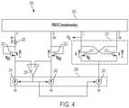
- FIG. 4shows an example of a negative resistance circuit using diode-connected transistors, according to some embodiments.
- FIG. 5shows an example of a complementary PMOS circuit, according to some embodiments.
- FIG. 6shows an example of a negative resistance circuit using diode-connected transistors and explicit impedances Z, according to some embodiments.
- Op-ampshave internal noise that may appear in the output signal. Although an op-amp may be designed to have reduced internal noise, doing so may increase power dissipation. Accordingly, it is desirable to use a different technique to reduce the internal noise appearing in the output signal.
- FIG. 1illustrates that the internal noise may be modeled as a voltage source V NI in series with the non-inverting input.
- the shunt negative resistance ( ⁇ R 3 )produces a current of suitable polarity that flows through resistor R 2 to the output, and at least partially cancels the external noise.
- FIG. 2illustrates that the optimized normalized value of
- 0.5. Therefore, it is desirable to have the negative resistance value be close to but not equal to the optimal value for canceling the internal noise.
- One challenge with setting the negative resistance value close to the value that causes the circuit to go unstableis that variations in the component values due to process voltage or temperature (PVT variations) can result in the negative resistance value drifting to the value at which the circuit goes unstable. Accordingly, would be desirable for the negative resistance circuit to be insensitive to PVT variations.
- circuits described hereinproduce a small signal negative resistance value and are insensitive to PVT variations.
- cross-coupled transistorsmay be included that are constant-G m biased in strong inversion or weak inversion.
- FIG. 3shows an example of a negative resistance circuit 100 , according to some embodiments.
- Negative resistance circuit 100includes a first cross-coupled transistor circuit 110 , a second cross-coupled transistor circuit 120 , an op-amp 130 and a current source circuit 140 .
- the first cross-coupled transistor circuit 110may be connected to the inverting input of the op-amp of FIG. 1 , also referred to as the summing node V S .
- the first cross-coupled transistor circuit 110may be connected to the non-inverting input of op-amp 130 at terminal V X0 .
- the first cross-coupled transistor circuit 110includes a transistor 111 having its source connected to terminal V X0 and its drain connected to the summing node Vs.
- the first cross-coupled transistor circuit 110also includes a transistor 112 having its source connected to terminal V X0 and its drain connected to a ground terminal.
- Transistors 111 and 112have a channel width W and a length L, with a ratio W/L. As illustrated in FIG.
- transistors 111 and 112are cross-coupled, with the gate of one transistor being connected to the drain of the other transistor. More specifically, transistor 111 has its gate connected to the drain of transistor 112 and transistor 112 has its gate connected to the drain of transistor 111 .
- a biasing currentis provided to the first cross-coupled transistor circuit 110 by current source 141 , which is controlled by the output of op-amp 130 .
- the first cross-coupled transistor circuit 110may be biased using constant-G m biasing.
- the first-cross coupled transistor circuit 110may be biased in strong inversion or in weak inversion.
- the second cross-coupled transistor circuit 120may be connected to the inverting input of op-amp 130 at terminal V X1 .
- the second cross-coupled transistor circuit 120includes a transistor 121 having its source connected to terminal V X1 and its drain connected to the impedance 123 .
- the second cross-coupled transistor circuit 120also includes a transistor 122 having its source connected to terminal V X1 and its drain connected to the impedance 124 .
- Transistors 121 and 122have a channel width to length ratio of M times W/L. As illustrated in FIG. 3 , transistors 121 and 122 are cross-coupled, with the gate of one transistor being connected to the drain of the other transistor.
- transistor 121has its gate connected to the drain of transistor 122 and transistor 122 has its gate connected to the drain of transistor 121 .
- a biasing currentis provided to the first cross-coupled transistor circuit 120 by current source 142 , which is controlled by the output of op-amp 130 .
- the second cross-coupled transistor circuit 120may be biased using constant-G m biasing.
- the second cross-coupled transistor circuit 120may be biased in strong inversion or in weak inversion.
- Op-amp 130maintains V X1 and V X0 at the same voltage.
- the output of op-amp 130controls the current sources 142 and 141 . Accordingly, the negative resistance circuit 100 maintains its (small signal) resistance and is sensitive to PVT variations.
- FIG. 3shows a single ended version of a negative resistance circuit 100
- a differential version of the negative resistance circuitmay be used. For example, instead of connecting the drain of transistor 112 to a ground terminal, a differential signal may be provided across the drains of transistors 111 and 112 .
- FIG. 4shows another example of a negative resistance circuit 200 , according to some embodiments.
- An op-amp 230has its inverting input connected to the source of transistor 221 and its non-inverting input connected to the source of transistor 222 .
- Transistors 221 and 222are each diode connected: their gate is connected to their drain.
- Transistor 222has a width to length ratio of W/L.
- Transistor 221has a width to length ratio of M times W/L.
- the op-amp 230holds the sources of transistors 221 and 222 at the same voltage.
- Transistor 221is biased by a current source 241 , which is controlled by the output of the op-amp 230 .
- Transistor 222is biased by a current source 242 , which is controlled by the output of the op-amp 230 .
- Transistor 221is in series with an impedance 225 .
- Impedance 225may be connected between the drain of transistor 225 and ground.
- the drain of transistor 222may be coupled to ground.
- the transistors 221 and 222may form a diode-connected replica bias circuit that provides constant constant-G m biasing. Such a replica bias circuit may have the advantage of low power consumption.
- Another advanceis that the feedback loop for the constant-G m biasing can be isolated from the main feedback loop.
- a cross-coupled transistor circuit 210may be connected to the inverting input of the op-amp of FIG. 1 , also referred to as the summing node V S .
- the cross-coupled transistor circuit 210includes a transistor 211 having its source connected to current source 243 and its drain connected to the summing node V S .
- the first cross-coupled transistor circuit 210also includes a transistor 212 having its source connected to current source 243 and its drain connected to a ground terminal.
- Transistors 211 and 212each has a channel width to length ratio of K times W/L. As illustrated in FIG. 4 , transistors 211 and 212 are cross-coupled, with the gate of one transistor being connected to the drain of the other transistor.
- transistor 211has its gate connected to the drain of transistor 212 and transistor 212 has its gate connected to the drain of transistor 211 .
- a biasing currentis provided to the cross-coupled transistor circuit 210 by current source 243 , which is controlled by the output of op-amp 230 .
- the cross-coupled transistor circuit 210may be biased using constant-G m biasing.
- the cross-coupled transistor circuit 210may be biased in strong inversion or in weak inversion.
- An optional PMOS complementary circuit 250may be included. Circuit 250 may enhance the overall Gm of the cross-coupled transistors 211 and 212 . NMOS transistors can sink current and PMOS transsitors can push current. Gm will be double for the same current if a PMOS device is also included.
- FIG. 6illustrates that optionally, an explicit impedance Z may be connected between the sources of transistors 211 and 212 and/or between the sources of transistors 221 and 222 . If the sources of transistors 211 and 212 are separated by an impedance Z the current source 243 may be split into two separate current sources 243 a and 243 b for biasing transistors 211 and 212 , respectively.
Landscapes
- Engineering & Computer Science (AREA)
- Power Engineering (AREA)
- Amplifiers (AREA)
Abstract
Description
Claims (20)
Priority Applications (4)
| Application Number | Priority Date | Filing Date | Title |
|---|---|---|---|
| US16/840,537US11228283B2 (en) | 2019-04-08 | 2020-04-06 | Negative impedance circuit for reducing amplifier noise |
| EP20168573.2AEP3723283B1 (en) | 2019-04-08 | 2020-04-07 | Negative impedance circuit for reducing amplifier noise |
| CN202110363126.5ACN113497590A (en) | 2020-04-06 | 2021-04-02 | Circuit for reducing noise of amplifier and negative impedance circuit |
| TW110112319ATWI758155B (en) | 2020-04-06 | 2021-04-06 | Circuit for reducing amplifier noise and negative impedance |
Applications Claiming Priority (2)
| Application Number | Priority Date | Filing Date | Title |
|---|---|---|---|
| US201962830639P | 2019-04-08 | 2019-04-08 | |
| US16/840,537US11228283B2 (en) | 2019-04-08 | 2020-04-06 | Negative impedance circuit for reducing amplifier noise |
Publications (2)
| Publication Number | Publication Date |
|---|---|
| US20200321919A1 US20200321919A1 (en) | 2020-10-08 |
| US11228283B2true US11228283B2 (en) | 2022-01-18 |
Family
ID=70227911
Family Applications (1)
| Application Number | Title | Priority Date | Filing Date |
|---|---|---|---|
| US16/840,537ActiveUS11228283B2 (en) | 2019-04-08 | 2020-04-06 | Negative impedance circuit for reducing amplifier noise |
Country Status (2)
| Country | Link |
|---|---|
| US (1) | US11228283B2 (en) |
| EP (1) | EP3723283B1 (en) |
Families Citing this family (1)
| Publication number | Priority date | Publication date | Assignee | Title |
|---|---|---|---|---|
| CN116232234B (en)* | 2022-09-06 | 2025-08-15 | 苏州大学 | High-gain operational amplifier circuit based on negative resistance technology |
Citations (16)
| Publication number | Priority date | Publication date | Assignee | Title |
|---|---|---|---|---|
| US4001735A (en) | 1975-11-20 | 1977-01-04 | Northern Electric Company Limited | Single amplifier immittance network |
| EP0768533B1 (en) | 1995-10-11 | 2002-06-12 | SOCIETE NATIONALE D'ETUDE ET DE CONSTRUCTION DE MOTEURS D'AVIATION -Snecma | Differential charge amplifier for piezoelectric sensor |
| US20030034849A1 (en) | 2001-08-16 | 2003-02-20 | Sanduleanu Mihai Adrian Tiberiu | Ring oscillator stage |
| TW544995B (en) | 2002-08-09 | 2003-08-01 | Advanic Technologies Inc | Flash A/D converter with new autozeroing and interpolation possessing negative impedance compensation |
| US20050195672A1 (en)* | 2004-03-03 | 2005-09-08 | Sang-Bo Lee | Current sense amplifier circuits having a bias voltage node for adjusting input resistance |
| US20060114044A1 (en)* | 2004-11-30 | 2006-06-01 | Svilen Mintchev | Differential delay cell having controllable amplitude output |
| TW200726070A (en) | 2005-12-30 | 2007-07-01 | Ind Tech Res Inst | Transimpedance amplifier using negative impedance compensation |
| US20090010054A1 (en) | 2007-07-04 | 2009-01-08 | Hee Bok Kang | Semiconductor memory device with ferroelectric device |
| US20110241646A1 (en)* | 2010-03-31 | 2011-10-06 | Maxim Integrated Products, Inc. | Low Noise Bandgap References |
| US20130136211A1 (en)* | 2011-11-30 | 2013-05-30 | Jarkko Jussila | RF Front-End for Intra-Band Carrier Aggregation |
| US8963641B1 (en) | 2013-03-15 | 2015-02-24 | Maxim Integrated Products, Inc. | Source-series terminated differential line driver circuit |
| US20160156318A1 (en) | 2013-03-14 | 2016-06-02 | Quantance, Inc. | Self setting power supply using negative output impedance |
| US9621136B1 (en) | 2015-11-12 | 2017-04-11 | Nxp Usa, Inc. | Data sampler circuit with equalization function and method for sampling data |
| US20180138860A1 (en) | 2016-10-25 | 2018-05-17 | Shenzhen GOODIX Technology Co., Ltd. | Amplitude limiting oscillation circuit |
| US10003374B1 (en)* | 2017-11-29 | 2018-06-19 | National Cheng Kung University | Wireless radio frequency transceiver system for internet of things |
| US20200257946A1 (en)* | 2019-02-12 | 2020-08-13 | The Board Of Trustees Of The Leland Stanford Junior University | Resonance-based inductive communication via frequency sweeping |
- 2020
- 2020-04-06USUS16/840,537patent/US11228283B2/enactiveActive
- 2020-04-07EPEP20168573.2Apatent/EP3723283B1/enactiveActive
Patent Citations (17)
| Publication number | Priority date | Publication date | Assignee | Title |
|---|---|---|---|---|
| US4001735A (en) | 1975-11-20 | 1977-01-04 | Northern Electric Company Limited | Single amplifier immittance network |
| EP0768533B1 (en) | 1995-10-11 | 2002-06-12 | SOCIETE NATIONALE D'ETUDE ET DE CONSTRUCTION DE MOTEURS D'AVIATION -Snecma | Differential charge amplifier for piezoelectric sensor |
| US20030034849A1 (en) | 2001-08-16 | 2003-02-20 | Sanduleanu Mihai Adrian Tiberiu | Ring oscillator stage |
| WO2003017487A1 (en) | 2001-08-16 | 2003-02-27 | Koninklijke Philips Electronics N.V. | Ring oscillator stage |
| TW544995B (en) | 2002-08-09 | 2003-08-01 | Advanic Technologies Inc | Flash A/D converter with new autozeroing and interpolation possessing negative impedance compensation |
| US20050195672A1 (en)* | 2004-03-03 | 2005-09-08 | Sang-Bo Lee | Current sense amplifier circuits having a bias voltage node for adjusting input resistance |
| US20060114044A1 (en)* | 2004-11-30 | 2006-06-01 | Svilen Mintchev | Differential delay cell having controllable amplitude output |
| TW200726070A (en) | 2005-12-30 | 2007-07-01 | Ind Tech Res Inst | Transimpedance amplifier using negative impedance compensation |
| US20090010054A1 (en) | 2007-07-04 | 2009-01-08 | Hee Bok Kang | Semiconductor memory device with ferroelectric device |
| US20110241646A1 (en)* | 2010-03-31 | 2011-10-06 | Maxim Integrated Products, Inc. | Low Noise Bandgap References |
| US20130136211A1 (en)* | 2011-11-30 | 2013-05-30 | Jarkko Jussila | RF Front-End for Intra-Band Carrier Aggregation |
| US20160156318A1 (en) | 2013-03-14 | 2016-06-02 | Quantance, Inc. | Self setting power supply using negative output impedance |
| US8963641B1 (en) | 2013-03-15 | 2015-02-24 | Maxim Integrated Products, Inc. | Source-series terminated differential line driver circuit |
| US9621136B1 (en) | 2015-11-12 | 2017-04-11 | Nxp Usa, Inc. | Data sampler circuit with equalization function and method for sampling data |
| US20180138860A1 (en) | 2016-10-25 | 2018-05-17 | Shenzhen GOODIX Technology Co., Ltd. | Amplitude limiting oscillation circuit |
| US10003374B1 (en)* | 2017-11-29 | 2018-06-19 | National Cheng Kung University | Wireless radio frequency transceiver system for internet of things |
| US20200257946A1 (en)* | 2019-02-12 | 2020-08-13 | The Board Of Trustees Of The Leland Stanford Junior University | Resonance-based inductive communication via frequency sweeping |
Non-Patent Citations (9)
| Title |
|---|
| Boutin N. Active compensation of op-amp inverting amplifier using NIC. Electronics Letters. Dec. 10, 1981;17(25):978-9. |
| Chen et al., Novel constant transconductance references and the comparisons with the traditional approach. Southwest Symposium on Mixed-Signal Design. Feb. 25, 2003:104-7. |
| EP 20168573.2, Sep. 8, 2020, Extended European Search Report. |
| Extended European Search Report dated Sep. 8, 2020 for European Application No. EP 20168573.2. |
| Jang et al., A 55μW 93.1 dB-DR 20kHz-BW single-bit CT ΔΣ modulator with negative R-assisted integrator achieving 178.7 dB FoM in 65nm CMOS. IEEE Symposium on VLSI Circuits Jun. 5, 2017:40-1. |
| Lee et al., A 1.2 V 68μW 98.2dB-DR audio continuous-time delta-sigma modulator. IEEE Symposium on VLSI Circuits Jun. 18, 2018:199-200. |
| Mahrof et al., Cancellation of OpAmp virtual ground imperfections by a negative conductance applied to improve RF receiver linearity. IEEE Journal of Solid-State Circuits. May 1, 2014:49(5):1112-24. |
| Talebbeydokhti et al., Constant transconductance bias circuit with an on-chip resistor. IEEE International Symposium on Circuits and Systems May 21, 2006:2857-60. |
| Wang et al., A 0.0004%(− 108dB) THD+ N, 112dB-SNR, 3.15 W fully differential Class-D audio amplifier with G m noise cancellation and negative output-common-mode injection techniques. IEEE International Solid-State Circuits Conference-(ISSCC) Feb. 11, 2018:58-60. |
Also Published As
| Publication number | Publication date |
|---|---|
| EP3723283A1 (en) | 2020-10-14 |
| US20200321919A1 (en) | 2020-10-08 |
| EP3723283B1 (en) | 2022-12-21 |
Similar Documents
| Publication | Publication Date | Title |
|---|---|---|
| US4554515A (en) | CMOS Operational amplifier | |
| US7474151B2 (en) | Active load with adjustable common-mode level | |
| US6437645B1 (en) | Slew rate boost circuitry and method | |
| KR950004709A (en) | MOS Differential Voltage-to-Current Conversion Circuit | |
| US4484148A (en) | Current source frequency compensation for a CMOS amplifier | |
| JPH0616571B2 (en) | Current amplifier | |
| US6525608B2 (en) | High gain, high bandwidth, fully differential amplifier | |
| US6788143B1 (en) | Cascode stage for an operational amplifier | |
| US6208199B1 (en) | Pulse amplifier with low duty cycle errors | |
| US6833760B1 (en) | Low power differential amplifier powered by multiple unequal power supply voltages | |
| US20080024219A1 (en) | Apparatus and method for biasing cascode devices in a differential pair using the input, output, or other nodes in the circuit | |
| US6236269B1 (en) | Complementary CMOS differential amplifier circuit | |
| US11228283B2 (en) | Negative impedance circuit for reducing amplifier noise | |
| US5043652A (en) | Differential voltage to differential current conversion circuit having linear output | |
| US4658219A (en) | Folded cascode field-effect transistor amplifier with increased gain | |
| US6278323B1 (en) | High gain, very wide common mode range, self-biased operational amplifier | |
| US6496066B2 (en) | Fully differential operational amplifier of the folded cascode type | |
| US6831501B1 (en) | Common-mode controlled differential gain boosting | |
| TWI758155B (en) | Circuit for reducing amplifier noise and negative impedance | |
| US20100295619A1 (en) | Low Noise Amplifier | |
| US7005921B2 (en) | Common-mode feedback circuit | |
| GB2193059A (en) | Voltage follower circuit | |
| US20150002209A1 (en) | Circuits for semiconductor device leakage cancellation | |
| US6583670B2 (en) | CMOS current amplifier | |
| US20240022213A1 (en) | Frequency compensation of amplifiers |
Legal Events
| Date | Code | Title | Description |
|---|---|---|---|
| FEPP | Fee payment procedure | Free format text:ENTITY STATUS SET TO UNDISCOUNTED (ORIGINAL EVENT CODE: BIG.); ENTITY STATUS OF PATENT OWNER: LARGE ENTITY | |
| AS | Assignment | Owner name:MEDIATEK SINGAPORE PTE. LTD., SINGAPORE Free format text:ASSIGNMENT OF ASSIGNORS INTEREST;ASSIGNORS:JEONG, TAEHOON;COONEY, PATRICK;SIGNING DATES FROM 20200511 TO 20200512;REEL/FRAME:052940/0392 | |
| STPP | Information on status: patent application and granting procedure in general | Free format text:APPLICATION DISPATCHED FROM PREEXAM, NOT YET DOCKETED | |
| STPP | Information on status: patent application and granting procedure in general | Free format text:DOCKETED NEW CASE - READY FOR EXAMINATION | |
| STPP | Information on status: patent application and granting procedure in general | Free format text:NON FINAL ACTION MAILED | |
| STPP | Information on status: patent application and granting procedure in general | Free format text:RESPONSE TO NON-FINAL OFFICE ACTION ENTERED AND FORWARDED TO EXAMINER | |
| STPP | Information on status: patent application and granting procedure in general | Free format text:NOTICE OF ALLOWANCE MAILED -- APPLICATION RECEIVED IN OFFICE OF PUBLICATIONS | |
| STPP | Information on status: patent application and granting procedure in general | Free format text:PUBLICATIONS -- ISSUE FEE PAYMENT VERIFIED | |
| STCF | Information on status: patent grant | Free format text:PATENTED CASE | |
| MAFP | Maintenance fee payment | Free format text:PAYMENT OF MAINTENANCE FEE, 4TH YEAR, LARGE ENTITY (ORIGINAL EVENT CODE: M1551); ENTITY STATUS OF PATENT OWNER: LARGE ENTITY Year of fee payment:4 |