US11227825B2 - High performance integrated RF passives using dual lithography process - Google Patents
High performance integrated RF passives using dual lithography processDownload PDFInfo
- Publication number
- US11227825B2 US11227825B2US15/773,030US201515773030AUS11227825B2US 11227825 B2US11227825 B2US 11227825B2US 201515773030 AUS201515773030 AUS 201515773030AUS 11227825 B2US11227825 B2US 11227825B2
- Authority
- US
- United States
- Prior art keywords
- conductive loop
- layer
- dielectric
- dielectric spacer
- conductive
- Prior art date
- Legal status (The legal status is an assumption and is not a legal conclusion. Google has not performed a legal analysis and makes no representation as to the accuracy of the status listed.)
- Active
Links
Images


Classifications
- H—ELECTRICITY
- H01—ELECTRIC ELEMENTS
- H01F—MAGNETS; INDUCTANCES; TRANSFORMERS; SELECTION OF MATERIALS FOR THEIR MAGNETIC PROPERTIES
- H01F17/00—Fixed inductances of the signal type
- H01F17/0006—Printed inductances
- H—ELECTRICITY
- H01—ELECTRIC ELEMENTS
- H01L—SEMICONDUCTOR DEVICES NOT COVERED BY CLASS H10
- H01L23/00—Details of semiconductor or other solid state devices
- H01L23/48—Arrangements for conducting electric current to or from the solid state body in operation, e.g. leads, terminal arrangements ; Selection of materials therefor
- H01L23/488—Arrangements for conducting electric current to or from the solid state body in operation, e.g. leads, terminal arrangements ; Selection of materials therefor consisting of soldered or bonded constructions
- H01L23/498—Leads, i.e. metallisations or lead-frames on insulating substrates, e.g. chip carriers
- H01L23/49838—Geometry or layout
- H—ELECTRICITY
- H01—ELECTRIC ELEMENTS
- H01F—MAGNETS; INDUCTANCES; TRANSFORMERS; SELECTION OF MATERIALS FOR THEIR MAGNETIC PROPERTIES
- H01F27/00—Details of transformers or inductances, in general
- H01F27/28—Coils; Windings; Conductive connections
- H01F27/2804—Printed windings
- H—ELECTRICITY
- H01—ELECTRIC ELEMENTS
- H01F—MAGNETS; INDUCTANCES; TRANSFORMERS; SELECTION OF MATERIALS FOR THEIR MAGNETIC PROPERTIES
- H01F27/00—Details of transformers or inductances, in general
- H01F27/40—Structural association with built-in electric component, e.g. fuse
- H—ELECTRICITY
- H01—ELECTRIC ELEMENTS
- H01F—MAGNETS; INDUCTANCES; TRANSFORMERS; SELECTION OF MATERIALS FOR THEIR MAGNETIC PROPERTIES
- H01F41/00—Apparatus or processes specially adapted for manufacturing or assembling magnets, inductances or transformers; Apparatus or processes specially adapted for manufacturing materials characterised by their magnetic properties
- H01F41/02—Apparatus or processes specially adapted for manufacturing or assembling magnets, inductances or transformers; Apparatus or processes specially adapted for manufacturing materials characterised by their magnetic properties for manufacturing cores, coils, or magnets
- H01F41/04—Apparatus or processes specially adapted for manufacturing or assembling magnets, inductances or transformers; Apparatus or processes specially adapted for manufacturing materials characterised by their magnetic properties for manufacturing cores, coils, or magnets for manufacturing coils
- H01F41/041—Printed circuit coils
- H—ELECTRICITY
- H01—ELECTRIC ELEMENTS
- H01G—CAPACITORS; CAPACITORS, RECTIFIERS, DETECTORS, SWITCHING DEVICES, LIGHT-SENSITIVE OR TEMPERATURE-SENSITIVE DEVICES OF THE ELECTROLYTIC TYPE
- H01G4/00—Fixed capacitors; Processes of their manufacture
- H01G4/33—Thin- or thick-film capacitors (thin- or thick-film circuits; capacitors without a potential-jump or surface barrier specially adapted for integrated circuits, details thereof, multistep manufacturing processes therefor)
- H—ELECTRICITY
- H01—ELECTRIC ELEMENTS
- H01L—SEMICONDUCTOR DEVICES NOT COVERED BY CLASS H10
- H01L21/00—Processes or apparatus adapted for the manufacture or treatment of semiconductor or solid state devices or of parts thereof
- H01L21/02—Manufacture or treatment of semiconductor devices or of parts thereof
- H01L21/04—Manufacture or treatment of semiconductor devices or of parts thereof the devices having potential barriers, e.g. a PN junction, depletion layer or carrier concentration layer
- H01L21/48—Manufacture or treatment of parts, e.g. containers, prior to assembly of the devices, using processes not provided for in a single one of the groups H01L21/18 - H01L21/326 or H10D48/04 - H10D48/07
- H01L21/4814—Conductive parts
- H01L21/4846—Leads on or in insulating or insulated substrates, e.g. metallisation
- H01L21/4857—Multilayer substrates
- H—ELECTRICITY
- H01—ELECTRIC ELEMENTS
- H01L—SEMICONDUCTOR DEVICES NOT COVERED BY CLASS H10
- H01L21/00—Processes or apparatus adapted for the manufacture or treatment of semiconductor or solid state devices or of parts thereof
- H01L21/02—Manufacture or treatment of semiconductor devices or of parts thereof
- H01L21/04—Manufacture or treatment of semiconductor devices or of parts thereof the devices having potential barriers, e.g. a PN junction, depletion layer or carrier concentration layer
- H01L21/48—Manufacture or treatment of parts, e.g. containers, prior to assembly of the devices, using processes not provided for in a single one of the groups H01L21/18 - H01L21/326 or H10D48/04 - H10D48/07
- H01L21/4814—Conductive parts
- H01L21/4846—Leads on or in insulating or insulated substrates, e.g. metallisation
- H01L21/486—Via connections through the substrate with or without pins
- H—ELECTRICITY
- H01—ELECTRIC ELEMENTS
- H01L—SEMICONDUCTOR DEVICES NOT COVERED BY CLASS H10
- H01L23/00—Details of semiconductor or other solid state devices
- H01L23/48—Arrangements for conducting electric current to or from the solid state body in operation, e.g. leads, terminal arrangements ; Selection of materials therefor
- H01L23/488—Arrangements for conducting electric current to or from the solid state body in operation, e.g. leads, terminal arrangements ; Selection of materials therefor consisting of soldered or bonded constructions
- H01L23/498—Leads, i.e. metallisations or lead-frames on insulating substrates, e.g. chip carriers
- H01L23/49822—Multilayer substrates
- H—ELECTRICITY
- H01—ELECTRIC ELEMENTS
- H01L—SEMICONDUCTOR DEVICES NOT COVERED BY CLASS H10
- H01L23/00—Details of semiconductor or other solid state devices
- H01L23/48—Arrangements for conducting electric current to or from the solid state body in operation, e.g. leads, terminal arrangements ; Selection of materials therefor
- H01L23/488—Arrangements for conducting electric current to or from the solid state body in operation, e.g. leads, terminal arrangements ; Selection of materials therefor consisting of soldered or bonded constructions
- H01L23/498—Leads, i.e. metallisations or lead-frames on insulating substrates, e.g. chip carriers
- H01L23/49827—Via connections through the substrates, e.g. pins going through the substrate, coaxial cables
- H—ELECTRICITY
- H01—ELECTRIC ELEMENTS
- H01L—SEMICONDUCTOR DEVICES NOT COVERED BY CLASS H10
- H01L23/00—Details of semiconductor or other solid state devices
- H01L23/58—Structural electrical arrangements for semiconductor devices not otherwise provided for, e.g. in combination with batteries
- H01L23/64—Impedance arrangements
- H01L23/66—High-frequency adaptations
- H01L28/00—
- H01L28/10—
- H01L28/60—
- H—ELECTRICITY
- H10—SEMICONDUCTOR DEVICES; ELECTRIC SOLID-STATE DEVICES NOT OTHERWISE PROVIDED FOR
- H10D—INORGANIC ELECTRIC SEMICONDUCTOR DEVICES
- H10D1/00—Resistors, capacitors or inductors
- H—ELECTRICITY
- H10—SEMICONDUCTOR DEVICES; ELECTRIC SOLID-STATE DEVICES NOT OTHERWISE PROVIDED FOR
- H10D—INORGANIC ELECTRIC SEMICONDUCTOR DEVICES
- H10D1/00—Resistors, capacitors or inductors
- H10D1/20—Inductors
- H—ELECTRICITY
- H10—SEMICONDUCTOR DEVICES; ELECTRIC SOLID-STATE DEVICES NOT OTHERWISE PROVIDED FOR
- H10D—INORGANIC ELECTRIC SEMICONDUCTOR DEVICES
- H10D1/00—Resistors, capacitors or inductors
- H10D1/60—Capacitors
- H10D1/68—Capacitors having no potential barriers
- H10D1/692—Electrodes
- H—ELECTRICITY
- H01—ELECTRIC ELEMENTS
- H01F—MAGNETS; INDUCTANCES; TRANSFORMERS; SELECTION OF MATERIALS FOR THEIR MAGNETIC PROPERTIES
- H01F27/00—Details of transformers or inductances, in general
- H01F27/28—Coils; Windings; Conductive connections
- H01F27/2804—Printed windings
- H01F2027/2809—Printed windings on stacked layers
- H—ELECTRICITY
- H01—ELECTRIC ELEMENTS
- H01L—SEMICONDUCTOR DEVICES NOT COVERED BY CLASS H10
- H01L2223/00—Details relating to semiconductor or other solid state devices covered by the group H01L23/00
- H01L2223/58—Structural electrical arrangements for semiconductor devices not otherwise provided for
- H01L2223/64—Impedance arrangements
- H01L2223/66—High-frequency adaptations
- H01L2223/6661—High-frequency adaptations for passive devices
Definitions
- Embodiments of the present inventionrelate generally to the manufacture of semiconductor devices.
- embodiments of the present inventionrelate to packages that include inductors with improved coupling and capacitors with improved capacitance density and methods for manufacturing such devices.
- Highly coupled transformers and high density capacitorsare useful in many radio frequency (RF) and power delivery applications.
- RFradio frequency
- more passive componentse.g., transformers and capacitors
- the current packaging design ruleslimit the optimization of some of the electrical properties of the components.
- the minimum allowable spacing between conductive lines in a packagemakes it difficult to achieve tightly coupled inductors in a small area.
- Coupling factors higher than about 0.5are difficult to achieve without consuming a relatively large area and large number of layers on the package.
- low coupling factorsare accounted for by using resonant transformers in RF by inserting a discrete capacitor in series or in parallel with the transformer to cancel the leakage inductance.
- resonant transformersare narrowband requiring additional transformers for other frequency bands.
- these transformersare implemented as discrete components on the package or on the main board.
- capacitorsare often used for amplifier tuning or antenna matching.
- capacitorscan be integrated into the packaging substrate layers.
- the packaging design rulestypically require relatively thick dielectric layers (e.g., 20 ⁇ m or greater) for separating the parallel plates of the capacitors. Since the capacitance is inversely proportional to the dielectric thicknesses, the capacitance per unit area is relatively small and the desired capacitance is obtained by increasing the package size or by using additional discrete capacitors.
- additional discrete capacitorsadds more routing parasitics and increases the losses. As such, the maximum operating frequency of the device may be reduced.
- FIG. 1is a perspective view of a package substrate that includes a transformer.
- FIG. 2Ais a plan view and a corresponding cross-sectional illustration of a package substrate with a dielectric layer that has a seed layer formed over the surface, according to an embodiment of the invention.
- FIG. 2Bis a plan view and a corresponding cross-sectional illustration of the package substrate after a first conductive loop is formed over a surface of the substrate, according to an embodiment of the invention.
- FIG. 2Cis a plan view and a corresponding cross-sectional illustration of the package substrate after a dielectric spacer is formed over the first conductive loop, according to an embodiment of the invention.
- FIG. 2Dis a plan view and a corresponding cross-sectional illustration of the package substrate after a second conductive loop is formed over the dielectric spacer, according to an embodiment of the invention.
- FIG. 2Eis a plan view and a corresponding cross-sectional illustration of the package substrate after the second photoresist material and the exposed portions of the seed layer have been removed, according to an embodiment of the invention.
- FIG. 3Ais a plan view and a corresponding cross-sectional illustration of a package substrate with a dielectric layer that has a seed layer formed over the surface, according to an embodiment of the invention.
- FIG. 3Bis a plan view and a corresponding cross-sectional illustration of the package substrate after a first conductive loop is formed over a surface of the substrate, according to an embodiment of the invention.
- FIG. 3Cis a plan view and a corresponding cross-sectional illustration of the package substrate after a dielectric spacer is formed over the first conductive loop, according to an embodiment of the invention.
- FIG. 3Dis a plan view and a corresponding cross-sectional illustration of the package substrate after a second conductive loop is formed within the perimeter of the first conductive loop, according to an embodiment of the invention.
- FIG. 3Eis a plan view and a corresponding cross-sectional illustration of the package substrate after the second photoresist material and the exposed portions of the seed layer have been removed, according to an embodiment of the invention.
- FIG. 4Ais a cross-sectional illustration of a package substrate after a first conductive loop is formed in a patterned photoresist layer, according to an embodiment of the invention.
- FIG. 4Bis a cross-sectional illustration of a package substrate after a cap dielectric is formed over the first conductive loop, according to an embodiment of the invention.
- FIG. 4Cis a cross-sectional illustration of a package substrate after the photoresist layer is removed and a sidewall dielectric is blanket deposited over the exposed surfaces, according to an embodiment of the invention.
- FIG. 4Dis a cross-sectional illustration of a package substrate after the sidewall dielectric layer is etched to provide sidewall dielectric spacers along the sidewalls of the first conductive loop, according to an embodiment of the invention.
- FIG. 5Ais a cross-sectional view of a package substrate that includes a parallel plate capacitor formed within a single dielectric layer, according to an embodiment of the invention.
- FIG. 5Bis a cross-sectional view of a capacitor with interdigitated extensions that may be included in a layer of a packaging substrate, according to an embodiment of the invention.
- FIG. 5Cis a perspective view of a portion of a first conductive plate that may be used in a capacitor with interdigitated extensions, according to an embodiment of the invention.
- FIG. 5Dis a perspective view of a capacitor with interdigitated extensions, according to an additional embodiment of the invention.
- FIG. 6Ais a cross-sectional illustration of a package substrate with a dielectric layer that has a seed layer formed over the surface, according to an embodiment of the invention.
- FIG. 6Bis a cross-sectional illustration of the package substrate after a first meandering plate is formed over a surface of the substrate, according to an embodiment of the invention.
- FIG. 6Cis a cross-sectional illustration of the package substrate after a dielectric spacer layer is formed over the first meandering plate, according to an embodiment of the invention.
- FIG. 6Dis a cross-sectional illustration of the package substrate after the exposed portions of the seed layer are removed, according to an embodiment of the invention.
- FIG. 6Eis a cross-sectional illustration of the package substrate after a patterned photoresist material is formed over the surface and a second seed layer is formed over the dielectric spacer layer, according to an embodiment of the invention.
- FIG. 6Fis a cross-sectional illustration of the package substrate after a second meandering plate is formed over the dielectric spacer layer, according to an embodiment of the invention.
- FIG. 6Gis a cross-sectional illustration of the package substrate after a second dielectric layer is deposited over the surface of the package, according to an embodiment of the invention.
- FIG. 7is a schematic of a computing device built in accordance with an embodiment of the invention.
- Described hereinare systems that include a semiconductor package and methods of forming such semiconductor packages.
- various aspects of the illustrative implementationswill be described using terms commonly employed by those skilled in the art to convey the substance of their work to others skilled in the art.
- the present inventionmay be practiced with only some of the described aspects.
- specific numbers, materials and configurationsare set forth in order to provide a thorough understanding of the illustrative implementations.
- the present inventionmay be practiced without the specific details.
- well-known featuresare omitted or simplified in order not to obscure the illustrative implementations.
- Embodiments of the inventioninclude transformer and capacitor structures that are formed with a fabrication technique that is compatible with semi-additive manufacturing process.
- integrated transformersmay be formed that have coupling coefficients that are greater than approximately 0.5.
- embodiments of the inventionmay include integrated capacitors that have a capacitance density that is at least an order of magnitude greater than capacitors that can be formed with currently available technologies.
- transformers that are integrated into packaginginclude a first conductive loop 115 A formed over the first dielectric layer 105 and a second conductive loop 115 B that is formed over a second dielectric layer 106 (the second dielectric layer 106 is illustrated as an invisible layer outlined by dashed lines in order to not unnecessarily obscure other aspects of the Figure). Accordingly, the distance D separating the two conductive loops is dependent on the thickness of the second dielectric layer 106 .
- the coupling factoris defined by Equation 1, where L 11 is the self-inductance of the first conductive loop 115 A , L 22 is the self-inductance of the second conductive loop 115 B and L 12 is the mutual inductance of the first conductive loop 115 A and the second conductive loop 115 B .
- the second dielectric layer 106may have a thickness of approximately 25 ⁇ m or greater.
- the coupling factormay be approximately 0.45 or less.
- embodiments of the inventionutilize processing operations that allow for the distance D between the conductive loops to be significantly decreased.
- the distance D between the loopsmay be decreased to less than 20 ⁇ m, which provides a coupling factor that may be greater than 0.5.
- Additional embodimentsmay include a distance D that is less than 1 ⁇ m.
- the coupling factormay be increased to over 0.7.
- the package layermay include a dielectric layer 205 that has a seed layer 235 formed over the top surface.
- the dielectric layer 205may be a polymer material, such as, for example, polyimide, epoxy, or build-up film (BF).
- the dielectric layer 205may be one layer in a stack that includes a plurality of dielectric layers used to form a build-up structure. As such, the dielectric layer 205 may be formed over another dielectric layer. Additional embodiments may include forming the dielectric layer 205 as the first dielectric layer over a core material on which the stack is formed.
- the seed layer 235may be a copper seed layer.
- a photoresist material 285may be formed over the seed layer 235 and patterned to provide openings for the formation of a first conductive loop 215 A .
- the patterning of the photoresist material 285may be implemented with lithographic processes (e.g., exposed with a radiation source through a mask (not shown) and developed with a developer).
- the first conductive loop 215 Amay be formed.
- the first conductive loop 215 Amay be formed with an electroplating process or the like.
- first conductive loop 215 Amay include forming a plurality of first conductive loops 215 A and that the first conductive loops 215 A may be formed at the same time as other conductive lines (e.g., signal lines or the like) that are formed over the first dielectric layer 205 .
- the first conductive loops 215 Amay be any desired shape.
- the first conductive loops 215 Amay each be a spiral shape with multiple turns.
- the first photoresist material 285is stripped and the exposed portions of the seed layer 235 are etched back with a seed etching process.
- embodiments of the inventioninclude forming a dielectric spacer layer 216 over the surfaces of the first conductive loop 215 A .
- the dielectric spacer layer 216provides the spacing between the first conductive loop 215 A and a second conductive loop 215 B that will be formed in a subsequent processing operation.
- the coupling factor of a transformermay be increased by decreasing the distance between the first and second conductive loops. Accordingly, controlling the thickness D of the dielectric spacer layer 216 provides the desired coupling factor.
- the dielectric spacer layer 216may have a thickness that provides a coupling factor that is approximately 0.5 or greater. In an embodiment, the thickness D may be less than 20 ⁇ m. In some embodiments the thickness D may be less than 5 ⁇ m.
- Embodiments of the inventionare able to form a dielectric spacer layer 216 with a controlled thickness D with any suitable deposition process.
- the dielectric spacer layer 216may be formed with a screen printing process. The screen printing process may optionally be performed prior to removing the first photoresist material 285 in order to improve alignment.
- the dielectric spacer layer 216 formedmay be omitted from the sidewalls of the first conductive loop 215 A .
- Additional embodimentsmay include a blanket deposition of the dielectric spacer layer 216 after the first photoresist material 285 has been removed. For example, a chemical vapor deposition (CVD) process may be used.
- CVDchemical vapor deposition
- the blanket dielectric spacer layer 216may then be patterned to remove portions of the dielectric spacer layer 216 from over the first dielectric layer 205 . Exposing the first dielectric layer 205 may provide better adhesion for subsequently deposited packaging layers.
- a second conductive loop 215 Bis formed over the dielectric spacer layer 216 .
- a second seed layer 236is formed.
- the second seed layer 236may be a copper seed layer that is blanket deposited.
- the metallic deposition used to form the second conductive loop 215 Bmay be isolated to over the first conductive loop 215 B by depositing and patterning a second photoresist material 286 to form openings over the second seed layer 236 .
- the second conductive loop 215 Bmay be formed with an electroplating process or the like.
- embodiments of the inventionmay include forming a plurality of second conductive loops 215 B and that the second conductive loops 215 B may be formed at the same time as other conductive features.
- the second conductive loop 215 Bmay be formed at the same time one or more vias are formed.
- the second photoresist material 286is stripped and the exposed portions of the second seed layer 236 are removed.
- the second seed layer 236may be removed with a seed etching process.
- Embodimentsmay then include forming a second dielectric layer 295 over the first and second conductive loops 215 A and 215 B .
- the second dielectric layer 295is omitted from the plan view for clarity.
- the second dielectric layer 295may be formed with any suitable process, such as lamination or slit coating and curing.
- first and second conductive loopsmay have thickness that are greater than the thickness of a single routing layer.
- the conductive loopsmay still be separated by a dielectric spacer layer substantially similar to dielectric spacer layer 216 described above.
- the coupling factormay still be greater than approximately 0.5. Increasing the thicknesses of the conductive loops would also provide a decrease in the resistance of the transformer while still maintaining the same inductance.
- a transformer with a high coupling factormay also be formed with the first and second conductive loops having a side-by-side configuration.
- the second conductive loopmay be formed within a perimeter of the first conductive loop.
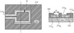
- the packagemay include a dielectric layer 305 that has a seed layer 335 formed over the top surface.
- the dielectric layer 305 and the seed layer 335may be substantially similar to the dielectric layer 205 that has a seed layer 235 described above, and therefore, will not be repeated here in detail.
- a photoresist material 385may be formed over the seed layer 335 and patterned to provide openings for the formation for a first conductive loop 315 A .
- Patterning the photoresist and forming the first conductive loop 315 Amay be substantially similar to the processing described above with respect to FIG. 2B , and therefore, will not be repeated here in detail. It is to be appreciated that while only a single first conductive loop 315 A is illustrated in the plan view, embodiments of the invention may include forming a plurality of first conductive loops 315 A and that the first conductive loops 315 A may be formed at the same time as other conductive lines (e.g., signal lines or the like) that are formed over the first dielectric layer 305 .
- other conductive linese.g., signal lines or the like
- the first photoresist material 385is stripped and a dielectric spacer layer 316 may be formed over the surfaces of the first conductive loop 315 A .
- the dielectric spacer layer 316provides the spacing between the first conductive loop 315 A and a second conductive loop 315 B that will be formed in a subsequent processing operation.
- the coupling factor of a transformermay be increased by decreasing the distance between the first and second conductive loops. Since the second conductive loop 315 B will be formed alongside the first conductive loop 315 A (i.e., the sidewalls of each loop will face each other), the thickness T of the sidewall portion of the dielectric spacer 316 needs to be controllable in order provide the desired coupling factor.
- the dielectric spacer layer 316may have a thickness T along the sidewalls of the first conductive loop 315 A that provides a coupling factor that is approximately 0.5 or greater. In an embodiment, the thickness T may be less than 20 ⁇ m. In some embodiments the thickness T may be less than 5 ⁇ m.
- the dielectric spacer layer 316is illustrated as being a single material. However embodiments are not limited to such a configuration.
- the sidewall portions of the dielectric spacer layer 316may be a different material than the portion formed on the top surface of the conductive loop.
- a process flow according to one embodiment of the invention that includes such a dielectric spacer layeris illustrated in FIGS. 4A-4D .
- FIG. 4Aa cross-sectional view of a first conductive loop 315 A is illustrated according to an embodiment of the invention.
- the conductive loop 315 Amay be substantially similar to the conductive loop 315 A illustrated in FIG. 3B .
- a top surface of the first conductive loop 315 Ais recessed below a top surface of the first photoresist layer 385 .
- a dielectric cap layer 316 Amay be selectively deposited over the top surfaces of the first conductive loop 315 A .
- the dielectric cap layer 316 Amay be formed with a stencil printing process, or any other suitable deposition process. Since the second conductive loop 315 B will be formed side-by-side with the first conductive loop 315 A , the thickness of the dielectric cap layer 316 A does not need to be as thin as the sidewall portions of the dielectric spacer layer 316 formed in a subsequent processing operation.
- the first photoresist material 385is stripped and a sidewall dielectric spacer layer 316 B is blanket deposited over the exposed surfaces.
- the sidewall dielectric layermay be any suitable material that can be conformally deposited in a layer that has a thickness T small enough to provide the desired coupling factor in the side-by-side transformer.
- the thickness Tmay be less than 20 ⁇ m. Additional embodiments may include a thickness T that is less than 10 ⁇ m.
- the sidewall dielectric spacer layer 316 Bmay be deposited with a CVD or any other blanket deposition process.
- the sidewall dielectric spacer layer 316 Bis removed from the horizontal surfaces.
- the sidewall dielectric spacer layer 316 Bmay be selectively removed from the horizontal surfaces with an anisotropic etching process, such as a reactive ion etching (RIE) process.
- RIEreactive ion etching
- the selective etching processallows for only portions of the sidewall dielectric spacer 316 B to remain along the sidewalls of the first conductive loop 315 A .
- the dielectric cap layer 316 Amay be a material that is resistant to the etching process used to selectively etch the sidewall dielectric spacer 316 B .
- the dielectric cap layer 316 Amay serve as an etch stop that prevents portions of the top surface of first conductive loop 315 A from being exposed. Protecting the top surface of the first conductive loop 315 A allows for an increased margin of error in the alignment of a patterning operation that will be used to form the second conductive loop 315 B , as will be described in greater detail below.
- the processing flowmay continue after the dielectric spacer 316 is formed over the first conductive loop 315 A .
- the dielectric spacer 316is depicted as being a single material, though it is to be appreciated that embodiments of the invention may include a dielectric spacer 316 that includes a dielectric cap layer 316 A and a sidewall dielectric spacer 316 B substantially similar to the one described above with respect to FIG. 4D .
- a second conductive loop 315 Bis formed alongside the first conductive loop 315 A .
- the metallic deposition used to form the second conductive loop 315 Bmay be done by depositing and patterning a second photoresist material 386 to form openings over the seed layer 335 .
- the openingsmay have a width W that extends over a top surface of the first conductive loop 315 A .
- the second conductive loop 315 Bmay be formed in direct contact with the sidewall portion of the dielectric spacer layer 316 without the need for highly accurate patterning of the photoresist layer.
- the spacing between the sidewall of the first conductive loop 315 A and the sidewall of the second conductive loop 315 Bmay be limited only by the minimum thickness T of the sidewall portion of the dielectric spacer 316 instead of by the design rules for the fabrication of interconnect lines in the package.
- the second conductive loop 315 Bis formed inside a perimeter of the first conductive loop 315 A .
- embodimentsare not limited to such configurations.
- the second conductive loop 315 Bmay optionally be formed along the outer sidewalls of the first conductive loop 315 A .
- the second photoresist material 386is stripped and the exposed portions of the seed layer 335 are removed.
- the seed layer 335may be removed with a seed etching process.
- Embodimentsmay then include forming a second dielectric layer (not shown) over the first and second conductive loops 315 A and 315 B .
- the second dielectric layermay be formed with any suitable process, such as lamination or slit coating and curing.
- Additional embodiments of the inventionmay also include forming integrated capacitors with high capacitance density.
- the high capacitance densityprovided by embodiments of the invention allows for a decrease in the area of the capacitors, which results in a decrease in cost and/or a reduction in the overall size of the package.
- the capacitance density of a capacitorcan be increased in a couple different ways. First, the surface area of the first and second capacitor plates that face each other can be increased. This may be accomplished by forming interdigitated stubs (e.g., a square meandering pattern, a saw tooth pattern, or the like) in the conductive plates. Additionally, the capacitance density can be increased to a much greater extent by decreasing the thickness of the dielectric layer that separates the first and second capacitor plates.
- the thickness of the dielectric layer that separates the capacitor plates in currently available capacitorsis limited by the thickness of the dielectric layers used to form each routing layer. As noted above, this thickness is typically about 25 ⁇ m or greater. As such, the capacitance density of currently available integrated capacitors is less than about 2 pF/mm 2 . Accordingly, embodiments of the invention may use processing operations that allow for the distance between the first and second capacitor plates to be significantly reduced. Examples of capacitors formed in accordance with embodiments of the invention are illustrated and described with respect to FIGS. 5A-5D .
- the capacitor 540includes a first capacitor plate 525 A formed over a dielectric layer 505 .
- the second conductive plate 525 Bis separated from the first capacitor plate 525 A by a dielectric spacer 516 .
- the distance separating the two capacitor platesmay be dictated by the thickness of the dielectric spacer 516 .
- the dielectric spacer 516may be less than 20 ⁇ m. As such, the entire capacitor may be formed within a single routing layer 506 of the package. Additional embodiments allow for the dielectric spacer 516 to be reduced in thickness to less than 1 ⁇ m. As such, the capacitance density can be increased by one or more orders of magnitude compared to currently available devices. For example, the capacitance density of a parallel plate capacitor according to embodiments of the invention may be approximately 200 pF/mm 2 or greater.
- FIG. 5Ba cross-sectional view of a capacitor with interdigitated extensions is shown according to an embodiment of the invention.
- portions of the packagee.g., the packaging layers and other conductive lines and vias
- the first capacitor plate 525 Amay include first extensions 517 that extend up from a seed layer 535 .
- the second capacitor plate 525 Bmay also include second extensions 519 that are interdigitated with the first extensions 517 .
- the two capacitor platesare separated by a dielectric spacer 516 .
- the interdigitated extensionsare self-aligned with each other. This allows for the pitch of the extensions to be decreased without needing to account for misalignment between layers. Accordingly, embodiments of the invention may increase the capacitance density to even greater extents than available with planar capacitors formed according to an embodiment of the invention.
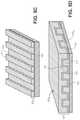
- FIG. 5Ca perspective view of a first capacitor plate 525 A with a meandering pattern formed in the X-Z plane (i.e., a two-dimensional square meander pattern) is shown, according to an embodiment of the invention.
- the dielectric spacer 516 and the second capacitor plateare omitted in order to not obscure the square meander pattern.
- the extensions 517are formed in the X-Z plane and extend continuously to the ends of the plate in the Y-direction.
- the interdigitated square meander pattern of the first capacitor plate 525 A and the second capacitor plate 525 Bis formed in the X, Y, and Z dimensions (i.e., a three-dimensional square meander pattern).
- FIGS. 6A-6DA process flow for forming a square meander capacitor according to such an embodiment is illustrated in FIGS. 6A-6D .
- the process flow illustrated in the Figuresdepicts a cross-sectional view of the meandering patterned capacitor.
- the processing illustrated in FIGS. 6A-6Dmay be used to form either a two-dimensional meandering pattern similar to the device illustrated in FIG. 5C or a three-dimensional pattern similar to the device illustrated in FIG. 5D .
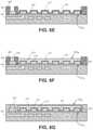
- the packagemay include a dielectric layer 605 that has a seed layer 635 formed over the top surface.
- the dielectric layer 605may be a polymer material, such as, for example, polyimide, epoxy, or BF.
- the dielectric layer 605may be one layer in a stack that includes a plurality of dielectric layers used to form a build-up structure. As such, the dielectric layer 605 may be formed over another dielectric layer that includes interconnect lines and vias 691 . Additional embodiments may include forming the dielectric layer 605 as the first dielectric layer over a core material on which the stack is formed.
- the seed layer 635may be a copper seed layer.
- a photoresist material 685may be formed over the seed layer 635 and patterned to provide openings for the formation for a via pad 692 and the first capacitor plate 625 A .
- the patterning of the photoresist material 685may be implemented with lithographic processes (e.g., exposed with a radiation source through a mask (not shown) and developed with a developer).
- the first capacitor plate 625 Amay be formed with an suitable deposition process, such as an electroplating process or the like. It is to be appreciated that while only the first capacitor plate 625 A is illustrated in FIG.
- embodiments of the inventionmay include forming a plurality of first capacitor plates 625 A and that the first capacitor plates 625 A may be formed at the same time as other conductive lines (e.g., signal lines or the like) may be formed over the first dielectric layer 605 .
- the first capacitor plate 625 Amay include a plurality of first extensions 617 .
- Each of the extensionsmay extend up from the seed layer 635 .
- each of the first extensions 617may be electrically coupled to each other by the seed layer 635 .
- the pitch of the extensions 617may be approximately 100 ⁇ m or smaller. Additional embodiments of the invention may include extensions 617 that have a pitch of approximately 20 ⁇ m or smaller.
- a dielectric spacer layer 616is formed over the surfaces of the first capacitor plate 625 A .
- the dielectric spacer layer 616provides the spacing between the first capacitor plate 625 A and a second capacitor plate 625 B that will be formed in a subsequent processing operation.
- the capacitance density of the capacitor formed by the first and second capacitor platesmay be increased by decreasing the distance between the first and second capacitor plates. Accordingly, controlling the thickness T of the dielectric spacer layer 616 will provide the desired capacitance density for the capacitor.
- the dielectric spacer layer 616may have thickness T that provides a capacitance density that is approximately 10 pF/mm 2 when the thickness T of the dielectric spacer layer is approximately 10 ⁇ m or less.
- embodiments of the inventionmay produce a significantly higher capacitance density by reducing the thickness T of the dielectric spacer layer 616 even further.
- capacitance densities ofmay be approximately 400 pF/mm 2 or greater when the thickness T of the dielectric spacer layer 616 is reduced to below 1 ⁇ m.
- Embodiments of the inventionare able to form a dielectric spacer layer 616 with a controlled thicknesses T with any suitable deposition process.
- the dielectric spacer layer 616may be formed with a screen printing process.
- Additional embodimentsmay include a blanket deposition of the dielectric spacer layer 616 .
- a CVD processmay be used.
- the blanket dielectric spacer layer 616may then be patterned to remove portions of the dielectric spacer layer 616 from over regions of the device (e.g., from over portions of the seed layer 635 that will not be a part of the first capacitor plate 625 A and over the via pad 692 ).
- Additional embodimentsmay include lamination of a thin dielectric build up layer followed by selective patterning and removal. Further embodiments may include lamination of a photo-definable dielectric material which is then removed using lithographic exposure and developing.
- the remaining portions of the seed layer 635 that are exposed after the dielectric spacer 616 is formedmay be removed.
- the seed layer 635may be removed with a seed layer etching process.
- the seed layer etching processelectrically isolates the first capacitor plate 625 A from other conductive components (e.g., the via pad 692 ) formed over the first dielectric layer 605 .
- a second seed layer 636is formed over the dielectric spacer 616 .
- the second seed layer 616may be a copper seed layer that is blanket deposited.
- the second seed layer 636may be blocked from being formed over the exposed portions of the first dielectric layer 605 by depositing and patterning a second photoresist material 686 .
- the patterned openings of the second photoresist material 686may include an opening for where the second capacitor plate will be formed in addition to providing a pattern for where vias will be formed.
- the second photoresist material 686may include an opening over the via pad 692 .
- the second capacitor plate 625 Bmay be selectively formed over the second seed layer 636 with any suitable deposition process, such as an electroplating process or the like. Due to the selective deposition over the second seed layer 636 , the second capacitor plate 625 B is formed with second extensions 619 that are self-aligned and interdigitated with the first extensions 617 . Furthermore, it is to be appreciated that the metal deposition process used to form the second capacitor plate 625 B may also be used to simultaneously form any needed vias 693 . It is to be appreciated that while only the second capacitor plate 625 B and a single via 693 is illustrated in FIG. 6F , embodiments of the invention may include forming a plurality of second capacitor plates 625 B and a plurality of vias 693 or other conductive structures needed in the layer of the package.
- the second photoresist material 686is stripped and a second dielectric layer 606 may be formed over the second capacitor plate 625 B and the via 693 .
- the second dielectric layermay be formed with any suitable process, such as lamination or slit coating and curing.
- the second dielectric layer 606is formed to a thickness that will completely cover a top surface of the vias 693 and the second capacitor plate 625 B .
- each of the dielectric layersmay not be highly uniform.
- the second dielectric layer 606may be formed to a thickness that is greater than the combined height of the vias 693 and the via pads 692 to ensure that the proper thickness is reached across the entire substrate.
- a controlled etching processmay then be used to expose the top surface of the via 693 , as illustrated in FIG. 6G .
- the dielectric removal processmay include a wet etch, a dry etch (e.g., a plasma etch), a wet blast, or a laser ablation (e.g., by using excimer laser).
- the depth controlled dielectric removal processmay be performed only proximate to the via 693 .
- laser ablation of the second dielectric layer 606may be localized proximate to the location of the via 693 .
- the thickness of the second dielectric layer 606may be minimized in order to reduce the etching time required to expose the line via 693 .
- the vias 693may extend above the top surface of the second dielectric layer 606 and the controlled dielectric removal process may be omitted.
- the top surface of the second capacitor plate 625 Bis covered by the second dielectric layer 606 in some embodiments.
- the subsequently formed signal lines on the next layermay be formed directly above portions of the second capacitor plate 625 B .
- the second dielectric layer 606may be recessed to expose a top portion of the 625 B in addition to exposing a top portion of the via 693 .
- FIG. 7illustrates a computing device 700 in accordance with one implementation of the invention.
- the computing device 700houses a board 702 .
- the board 702may include a number of components, including but not limited to a processor 704 and at least one communication chip 706 .
- the processor 704is physically and electrically coupled to the board 702 .
- the at least one communication chip 706is also physically and electrically coupled to the board 702 .
- the communication chip 706is part of the processor 704 .
- computing device 700may include other components that may or may not be physically and electrically coupled to the board 702 .
- these other componentsinclude, but are not limited to, volatile memory (e.g., DRAM), non-volatile memory (e.g., ROM), flash memory, a graphics processor, a digital signal processor, a crypto processor, a chipset, an antenna, a display, a touchscreen display, a touchscreen controller, a battery, an audio codec, a video codec, a power amplifier, a global positioning system (GPS) device, a compass, an accelerometer, a gyroscope, a speaker, a camera, and a mass storage device (such as hard disk drive, compact disk (CD), digital versatile disk (DVD), and so forth).
- volatile memorye.g., DRAM
- non-volatile memorye.g., ROM
- flash memorye.g., a graphics processor, a digital signal processor, a crypto processor, a chipset, an
- the communication chip 706enables wireless communications for the transfer of data to and from the computing device 700 .
- wirelessand its derivatives may be used to describe circuits, devices, systems, methods, techniques, communications channels, etc., that may communicate data through the use of modulated electromagnetic radiation through a non-solid medium. The term does not imply that the associated devices do not contain any wires, although in some embodiments they might not.
- the communication chip 706may implement any of a number of wireless standards or protocols, including but not limited to Wi-Fi (IEEE 802.11 family), WiMAX (IEEE 802.16 family), IEEE 802.20, long term evolution (LTE), Ev-DO, HSPA+, HSDPA+, HSUPA+, EDGE, GSM, GPRS, CDMA, TDMA, DECT, Bluetooth, derivatives thereof, as well as any other wireless protocols that are designated as 3G, 4G, 5G, and beyond.
- the computing device 700may include a plurality of communication chips 706 .
- a first communication chip 706may be dedicated to shorter range wireless communications such as Wi-Fi and Bluetooth and a second communication chip 706 may be dedicated to longer range wireless communications such as GPS, EDGE, GPRS, CDMA, WiMAX, LTE, Ev-DO, and others.
- the processor 704 of the computing device 700includes an integrated circuit die packaged within the processor 704 .
- the integrated circuit die of the processorincludes one or more devices, such as devices that are packaged in a system that includes one or more integrated transformers and/or capacitors that are formed with a dielectric spacer layer, in accordance with implementations of the invention.
- the term “processor”may refer to any device or portion of a device that processes electronic data from registers and/or memory to transform that electronic data into other electronic data that may be stored in registers and/or memory.
- the communication chip 706also includes an integrated circuit die packaged within the communication chip 706 .
- the integrated circuit die of the communication chipincludes one or more devices, such as devices that are packaged in a system that includes one or more integrated transformers and/or capacitors that are formed with a dielectric spacer layer, in accordance with implementations of the invention.
- An embodiment of the inventionmay include a transformer formed in an electrical package comprising: a first dielectric layer; a first conductive loop formed over a surface of the first dielectric layer; a dielectric spacer formed over the first conductive loop; and a second conductive loop separated from the first conductive loop by the dielectric spacer layer.
- An additional embodiment of the inventionmay include a transformer formed in an electrical package, wherein the second conductive loop is formed above the first conductive loop.
- An additional embodiment of the inventionmay include a transformer formed in an electrical package, wherein the first conductive loop and the second conductive loop are formed in a single routing layer of the electrical package
- An additional embodiment of the inventionmay include a transformer formed in an electrical package, wherein the dielectric spacer layer is former only over a top surface of the first conductive loop.
- An additional embodiment of the inventionmay include a transformer formed in an electrical package, wherein the second conductive loop is formed over the first dielectric layer, and wherein a sidewall surface of the first conductive loop is separated from a sidewall surface of the second conductive loop by the dielectric spacer.
- An additional embodiment of the inventionmay include a transformer formed in an electrical package, wherein the dielectric spacer includes a cap layer formed over a top surface of the first conductive loop and a sidewall spacer formed over the sidewalls of the first conductive loop.
- An additional embodiment of the inventionmay include a transformer formed in an electrical package, wherein the cap layer is a different material than the sidewall spacer.
- An additional embodiment of the inventionmay include a transformer formed in an electrical package, wherein the second conductive loop is formed inside a perimeter of the first conductive loop.
- An additional embodiment of the inventionmay include a transformer formed in an electrical package, wherein the dielectric spacer layer has a thickness that is less than 20 ⁇ m.
- An additional embodiment of the inventionmay include a transformer formed in an electrical package, wherein the dielectric spacer layer has a thickness that is less than 5 ⁇ m.
- An embodiment of the inventionmay include a method of forming a transformer in an electrical package, comprising: forming a first conductive loop over a first dielectric layer; forming a dielectric spacer layer over the first conductive loop; and forming a second conductive loop in direct contact with the dielectric spacer layer, wherein the first conductive loop is spaced apart from the second conductive loop by only the dielectric spacer layer.
- An additional embodiment of the inventionmay include a method, wherein the second conductive loop is formed over a top surface of the first conductive loop.
- An additional embodiment of the inventionmay include a method, wherein forming the second conductive loop comprises: forming a seed layer over the dielectric spacer layer; depositing and patterning a photoresist material to form openings above the first conductive loop; and plating a conductive material in the openings.
- An additional embodiment of the inventionmay include a method, wherein the second conductive loop is formed side-by-side with the first conductive loop.
- An additional embodiment of the inventionmay include a method, wherein forming the dielectric spacer layer comprises: forming a cap layer over a top surface of the first conductive loop; forming a conformal spacer layer over the exposed surfaces; and etching the conformal spacer layer with an anisotropic etching process to remove the conformal spacer layer from horizontal surfaces, wherein a sidewall spacer remains along sidewalls of the first conductive loop.
- An embodiment of the inventionincludes a capacitor formed in an electrical package comprising: a first dielectric layer; a first capacitor plate formed over a surface of the first dielectric layer; a dielectric spacer formed over a surface of the first capacitor plate; and a second capacitor plate separated from the first capacitor plate by the dielectric spacer layer.
- An additional embodiment of the inventionincludes a capacitor formed in an electrical package, wherein the first and second capacitor plates are formed in a single routing layer of the package.
- An additional embodiment of the inventionincludes a capacitor formed in an electrical package, wherein the dielectric spacer is less than 10 ⁇ m thick.
- An additional embodiment of the inventionincludes a capacitor formed in an electrical package, wherein the first and second capacitor plates include interdigitated square meander extensions.
- An additional embodiment of the inventionincludes a capacitor formed in an electrical package, wherein the extensions are formed in three-dimensions.
- An embodiment of the inventionincludes a method for forming a capacitor in an electrical package, comprising: forming a first capacitor plate over a first dielectric layer; forming a dielectric spacer layer over the first capacitor plate; and forming a second capacitor plate in direct by with the dielectric spacer layer, wherein the first capacitor plate is spaced apart from the second capacitor plate by only the dielectric spacer layer.
- An additional embodiment of the inventionincludes a method, wherein forming the first capacitor plate comprises: forming a first seed layer over the first dielectric layer; depositing a photoresist material over the first seed layer; patterning the photoresist material to form one or more openings; and depositing a conductive material into the openings.
- An additional embodiment of the inventionincludes a method, wherein the dielectric spacer layer is formed with a screen printing process, a chemical vapor depositions process, a lamination process, or a photolithographic patterning of a photodefinable dielectric layer.
- An additional embodiment of the inventionincludes a method, wherein forming the second capacitor plate comprises: forming a second seed layer over a surface of the dielectric spacer layer; and growing the second capacitor plate form the second seed layer with an electroplating process.
- An additional embodiment of the inventionincludes a method, wherein the second capacitor plate is formed concurrently with the formation of one or more vias.
Landscapes
- Engineering & Computer Science (AREA)
- Power Engineering (AREA)
- Microelectronics & Electronic Packaging (AREA)
- Physics & Mathematics (AREA)
- Condensed Matter Physics & Semiconductors (AREA)
- General Physics & Mathematics (AREA)
- Computer Hardware Design (AREA)
- Manufacturing & Machinery (AREA)
- Ceramic Engineering (AREA)
- Geometry (AREA)
- Semiconductor Integrated Circuits (AREA)
Abstract
Description
Claims (9)
Applications Claiming Priority (1)
| Application Number | Priority Date | Filing Date | Title |
|---|---|---|---|
| PCT/US2015/067157WO2017111910A1 (en) | 2015-12-21 | 2015-12-21 | High performance integrated rf passives using dual lithography process |
Related Parent Applications (1)
| Application Number | Title | Priority Date | Filing Date |
|---|---|---|---|
| PCT/US2015/067157A-371-Of-InternationalWO2017111910A1 (en) | 2015-12-21 | 2015-12-21 | High performance integrated rf passives using dual lithography process |
Related Child Applications (1)
| Application Number | Title | Priority Date | Filing Date |
|---|---|---|---|
| US17/544,693DivisionUS12002745B2 (en) | 2015-12-21 | 2021-12-07 | High performance integrated RF passives using dual lithography process |
Publications (2)
| Publication Number | Publication Date |
|---|---|
| US20180315690A1 US20180315690A1 (en) | 2018-11-01 |
| US11227825B2true US11227825B2 (en) | 2022-01-18 |
Family
ID=59091077
Family Applications (2)
| Application Number | Title | Priority Date | Filing Date |
|---|---|---|---|
| US15/773,030ActiveUS11227825B2 (en) | 2015-12-21 | 2015-12-21 | High performance integrated RF passives using dual lithography process |
| US17/544,693Active2035-12-23US12002745B2 (en) | 2015-12-21 | 2021-12-07 | High performance integrated RF passives using dual lithography process |
Family Applications After (1)
| Application Number | Title | Priority Date | Filing Date |
|---|---|---|---|
| US17/544,693Active2035-12-23US12002745B2 (en) | 2015-12-21 | 2021-12-07 | High performance integrated RF passives using dual lithography process |
Country Status (3)
| Country | Link |
|---|---|
| US (2) | US11227825B2 (en) |
| TW (1) | TWI746483B (en) |
| WO (1) | WO2017111910A1 (en) |
Families Citing this family (2)
| Publication number | Priority date | Publication date | Assignee | Title |
|---|---|---|---|---|
| US10672693B2 (en) | 2018-04-03 | 2020-06-02 | Intel Corporation | Integrated circuit structures in package substrates |
| US20230361019A1 (en)* | 2022-05-03 | 2023-11-09 | Nanya Technology Corporation | Semiconductor device |
Citations (97)
| Publication number | Priority date | Publication date | Assignee | Title |
|---|---|---|---|---|
| US5015972A (en)* | 1989-08-17 | 1991-05-14 | Motorola, Inc. | Broadband RF transformer |
| US5065270A (en)* | 1989-05-17 | 1991-11-12 | Tdk Corporation | Thin film magnetic recording head with a low resistance coil formed by two processes |
| US5300903A (en)* | 1991-06-27 | 1994-04-05 | Murata Manufacturing Co., Ltd. | Band-pass filter |
| US5502430A (en)* | 1992-10-29 | 1996-03-26 | Hitachi, Ltd. | Flat transformer and power supply unit having flat transformer |
| US5652561A (en)* | 1993-06-29 | 1997-07-29 | Yokogawa Electric Corporation | Laminating type molded coil |
| US5793272A (en)* | 1996-08-23 | 1998-08-11 | International Business Machines Corporation | Integrated circuit toroidal inductor |
| US6185068B1 (en)* | 1998-07-10 | 2001-02-06 | Hitachi Metals, Ltd. | Thin-film magnetic head with a coil having a trapezoidal crosssection |
| US6191918B1 (en)* | 1998-10-23 | 2001-02-20 | International Business Machines Corporation | Embedded dual coil planar structure |
| US6246541B1 (en)* | 1998-05-29 | 2001-06-12 | Hitachi Metals, Ltd. | Thin film magnetic head with reduced magnetic gap by incorporating coil conductors with convex surfaces |
| US6307818B1 (en)* | 1998-06-09 | 2001-10-23 | Seagate Technology Llc | Magneto-optical head with integral mounting of lens holder and coil |
| US6369983B1 (en)* | 1999-08-13 | 2002-04-09 | Read-Rite Corporation | Write head having a dry-etchable antireflective intermediate layer |
| US20020044379A1 (en)* | 2000-10-16 | 2002-04-18 | Alps Electric Co., Ltd. | Thin-film magnetic head having thin coil-layer and method for manufacturing the thin-film magnetic head |
| US20020075116A1 (en)* | 2000-11-21 | 2002-06-20 | Peels Wilhelmus Gerardus Maria | System, printed circuit board, charger device, user device, and apparatus |
| US6437441B1 (en)* | 1997-07-10 | 2002-08-20 | Kawasaki Microelectronics, Inc. | Wiring structure of a semiconductor integrated circuit and a method of forming the wiring structure |
| US20020113682A1 (en)* | 2000-12-22 | 2002-08-22 | Spartak Gevorgian | Multilayer balun transformer structure |
| US20020191334A1 (en)* | 2001-06-18 | 2002-12-19 | Yimin Hsu | Magnetic transducer with pedestal pole piece structure |
| US20030001709A1 (en)* | 2001-06-29 | 2003-01-02 | Visser Hendrik Arend | Multiple-interleaved integrated circuit transformer |
| US6538846B1 (en)* | 1999-08-06 | 2003-03-25 | Alps Electric Co., Ltd. | Thin-film magnetic head and method for making the same |
| US20030137383A1 (en)* | 2002-01-23 | 2003-07-24 | Yang Hung Yu David | On-chip transformer balun |
| US20040027224A1 (en)* | 2002-05-31 | 2004-02-12 | International Rectifier Corporation | Planar transformer arrangement |
| US20040048132A1 (en)* | 2001-09-26 | 2004-03-11 | Yuichi Takai | Fuel cell and electronic device using fuel cell |
| US6734526B1 (en) | 2002-10-16 | 2004-05-11 | Taiwan Semiconductor Manufacturing Co., Ltd. | Oxidation resistant microelectronics capacitor structure with L shaped isolation spacer |
| US20040227608A1 (en)* | 2003-05-16 | 2004-11-18 | Toshifumi Nakatani | Mutual induction circuit |
| US20040232519A1 (en)* | 2001-08-14 | 2004-11-25 | Van Beek Jozef Thomas Martinus | Electronic device and method of testing and of manufacturing |
| US20050068148A1 (en)* | 2003-07-28 | 2005-03-31 | Tdk Corporation | Coil component and method of manufacturing the same |
| US20050068675A1 (en)* | 2003-09-30 | 2005-03-31 | Headway Technologies, Inc. | Thin film magnetic head and manufacturing method thereof |
| US20050083607A1 (en)* | 2003-10-16 | 2005-04-21 | Headway Technologies, Inc. | Thin film magnetic head and manufacturing method thereof |
| US20050104706A1 (en)* | 2003-11-18 | 2005-05-19 | Via Technologies, Inc. | Coplanar transformer with a capacitor |
| US20050128639A1 (en)* | 2003-10-10 | 2005-06-16 | Headway Technologies, Inc. | Thin film magnetic head and manufacturing method thereof |
| US6914509B2 (en)* | 2003-04-04 | 2005-07-05 | Via Technologies Inc. | Transformer former between two layout layers |
| US20050157423A1 (en)* | 2004-01-20 | 2005-07-21 | Headway Technologies, Inc. | Thin film magnetic head and manufacturing method thereof |
| US20050174209A1 (en)* | 2003-11-14 | 2005-08-11 | Canon Kabushiki Kaisha | Wiring structure, and fabrication method of the same |
| US20050185337A1 (en)* | 2004-02-23 | 2005-08-25 | Headway Technologies | Thin film magnetic head and manufacturing method thereof |
| US20060028313A1 (en)* | 2004-07-26 | 2006-02-09 | Infineon Technologies Ag | Component arrangement with a planar transformer |
| US20060077028A1 (en)* | 2004-10-08 | 2006-04-13 | Kai-Yi Huang | Integrated transformer with stack structure |
| US20060137174A1 (en)* | 2003-10-20 | 2006-06-29 | Headway Technologies, Inc. | Thin film magnetic head and manufacturing method thereof |
| US20060145869A1 (en)* | 2004-12-23 | 2006-07-06 | Checkpoint Systems, Inc. | Method and apparatus for protecting culinary products |
| US20060202789A1 (en)* | 2003-12-15 | 2006-09-14 | Nokia Corporation | Electrically decoupled integrated transformer having at least one grounded electric shield |
| US20070025586A1 (en)* | 2005-07-28 | 2007-02-01 | Young Larry J | Armored voice coil assembly for use in high power loudspeaker applications |
| US20070030659A1 (en)* | 2003-09-29 | 2007-02-08 | Yukiharu Suzuki | Multilayer laminated circuit board |
| US20070057755A1 (en)* | 2003-09-29 | 2007-03-15 | Yukiharu Suzuki | Solid electrolytic capacitor and manufacturing method thereof |
| US7298238B1 (en)* | 2006-12-15 | 2007-11-20 | The United States Of America As Represented By The Secretary Of The Navy | Programmable microtransformer |
| US20080013635A1 (en)* | 2004-06-03 | 2008-01-17 | Silicon Laboratories Inc. | Transformer coils for providing voltage isolation |
| US20080120828A1 (en) | 2006-11-28 | 2008-05-29 | Whitworth Adam J | High Density Planarized Inductor And Method Of Making The Same |
| US20080179963A1 (en)* | 2006-08-28 | 2008-07-31 | Avago Technologies Ecbu (Singapore) Pte. Ltd. | Galvanic Isolators and Coil Transducers |
| US20080197963A1 (en)* | 2007-02-15 | 2008-08-21 | Sony Corporation | Balun transformer, mounting structure of balun transformer, and electronic apparatus having built-in mounting structure |
| US20080309445A1 (en)* | 2007-06-14 | 2008-12-18 | Tdk Corporation | Transformer |
| US20090237175A1 (en)* | 2008-03-21 | 2009-09-24 | Yinon Degani | Compact balun transformers |
| US20090243783A1 (en)* | 2006-08-28 | 2009-10-01 | Avago Technologies Ecbu (Singapore) Pte. Ltd. | Minimizing Electromagnetic Interference in Coil Transducers |
| US20090243782A1 (en)* | 2006-08-28 | 2009-10-01 | Avago Technologies Ecbu (Singapore) Pte. Ltd. | High Voltage Hold-Off Coil Transducer |
| US20090289750A1 (en)* | 2006-10-31 | 2009-11-26 | Takashi Ohsawa | Sheet type transformer and discharge lamp lighting apparatus |
| US20090295528A1 (en)* | 2008-05-28 | 2009-12-03 | Arturo Silva | Ac/dc planar transformer |
| US20100020448A1 (en)* | 2006-08-28 | 2010-01-28 | Avago Technologies Ecbu Ip (Singapore) Pte. Ltd. | Galvanic isolator |
| US20100052838A1 (en)* | 2008-09-01 | 2010-03-04 | Murata Manufacturing Co., Ltd. | Electronic component |
| US20100259351A1 (en)* | 2006-09-12 | 2010-10-14 | Robert James Bogert | Low profile layered coil and cores for magnetic components |
| US20110012690A1 (en)* | 2009-06-30 | 2011-01-20 | Tdk Corporation | Thin film balun |
| US20110032065A1 (en)* | 2009-08-07 | 2011-02-10 | Imec | Two Layer Transformer |
| US20110109417A1 (en)* | 2008-04-22 | 2011-05-12 | Thales | Power transformer for radiofrequency signals |
| US20110148549A1 (en)* | 2009-12-23 | 2011-06-23 | Peter Kanschat | Signal Transmission Arrangement |
| US20110233776A1 (en)* | 2005-05-18 | 2011-09-29 | Megica Corporation | Semiconductor chip with coil element over passivation layer |
| US20110241160A1 (en)* | 2010-03-30 | 2011-10-06 | Martin Kerber | High Voltage Semiconductor Devices and Methods of Forming the Same |
| US20110291231A1 (en)* | 2010-05-27 | 2011-12-01 | Li Jiang | Method of manufacturing a semiconductor component and structure |
| US20120022393A1 (en)* | 2010-07-22 | 2012-01-26 | Christian Pruckner | Medical treatment device |
| US20120080770A1 (en)* | 2010-09-30 | 2012-04-05 | Uwe Wahl | Transformer Arrangement |
| US20120122293A1 (en) | 2009-11-16 | 2012-05-17 | International Business Machines Corporation | Method of forming mim capacitor structure in feol |
| US20120235780A1 (en)* | 2011-03-16 | 2012-09-20 | Delphi Technologies, Inc. | Planar magnetic structure |
| US20130082812A1 (en)* | 2011-09-30 | 2013-04-04 | Samsung Electro-Mechanics Co., Ltd. | Coil parts and method of fabricating the same |
| US20130082813A1 (en)* | 2011-09-30 | 2013-04-04 | Sung Kwon Wi | Coil parts |
| US20130265131A1 (en)* | 2012-04-05 | 2013-10-10 | Samsung Electro-Mechanics Co., Ltd. | Electronic component and method for manufacturing the same |
| US20130328164A1 (en)* | 2012-06-06 | 2013-12-12 | Jenhao Cheng | Inductor device and fabrication method |
| US8643219B2 (en)* | 2008-05-22 | 2014-02-04 | Mitsubishi Electric Corporation | Electronic equipment and method for connecting electronic circuit substrate |
| US20140055209A1 (en)* | 2011-05-09 | 2014-02-27 | Murata Manufacturing Co., Ltd. | Front-end circuit and communication terminal apparatus |
| US20140070420A1 (en)* | 2012-09-12 | 2014-03-13 | Infineon Technologies Ag | Chip To Package Interface |
| US20140078014A1 (en)* | 2011-05-31 | 2014-03-20 | Murata Manufacturing Co., Ltd. | Antenna device and communication terminal apparatus |
| US20140138792A1 (en) | 2012-11-21 | 2014-05-22 | Qualcomm Incorporated | Hybrid transformer structure on semiconductor devices |
| US20140145806A1 (en)* | 2012-11-29 | 2014-05-29 | Honeywell International Inc. | Electromagnetic coil assemblies having braided lead wires and/or braided sleeves and methods for the fabrication thereof |
| US20140176284A1 (en)* | 2012-12-26 | 2014-06-26 | Samsung Electro-Mechanics Co., Ltd. | Common mode filter and method of manufacturing the same |
| US20140198418A1 (en)* | 2013-01-15 | 2014-07-17 | Citruscom Corporation | Integrated circuit common-mode filters with esd protection and manufacturing method |
| US20140225698A1 (en)* | 2013-02-13 | 2014-08-14 | Nokia Corporation | Integrated transformer balun with enhanced common-mode rejection for radio frequency, microwave, and millimeter-wave integrated circuits |
| US8823466B2 (en)* | 2007-06-08 | 2014-09-02 | Stats Chippac, Ltd. | Miniaturized wide-band baluns for RF applications |
| US20140264734A1 (en)* | 2013-03-14 | 2014-09-18 | Taiwan Semiconductor Manufacturing Company, Ltd. | Inductor With Magnetic Material |
| US20140273825A1 (en)* | 2013-03-15 | 2014-09-18 | Infineon Technologies Ag | Semiconductor Chip Configuration with a Coupler |
| US20140313005A1 (en)* | 2013-04-18 | 2014-10-23 | Samsung Electro-Mechanics Co., Ltd. | Common mode filter and method of manufacturing the same |
| US20140347154A1 (en)* | 2013-05-21 | 2014-11-27 | Coherent, Inc. | Interleaved planar pcb rf transformer |
| US20150029623A1 (en)* | 2013-07-26 | 2015-01-29 | Samsung Electro-Mechanics Co., Ltd. | Common mode filter |
| US20150041190A1 (en)* | 2013-08-06 | 2015-02-12 | Texas Instruments Incorporated | High voltage polymer dielectric capacitor isolation device |
| US20150051541A1 (en)* | 2012-03-26 | 2015-02-19 | Sumitomo Bakelite Co., Ltd. | Medical instrument and method of manufacturing medical instrument |
| US20150069572A1 (en)* | 2013-09-12 | 2015-03-12 | Texas Instruments Incorporated | Multilayer High Voltage Isolation Barrier in an Integrated Circuit |
| US8994478B1 (en)* | 2013-11-22 | 2015-03-31 | Samsung Electro-Mechanics Co., Ltd. | Common mode filter |
| US9024713B1 (en)* | 2012-08-09 | 2015-05-05 | Power Distribution Products, Inc. | Extreme duty encapsulated transformer coil with corrugated cooling ducts and method of making the same |
| US20150188511A1 (en)* | 2012-09-28 | 2015-07-02 | Murata Manufacturing Co., Ltd. | Impedance conversion circuit and antenna device |
| US20150202409A1 (en)* | 2012-08-03 | 2015-07-23 | Sumitomo Bakelite Co., Ltd. | Medical instrument, and medical-instrument production method |
| US20150282308A1 (en)* | 2014-03-28 | 2015-10-01 | Thorsten Meyer | Passive electrical devices with a polymer carrier |
| US9183977B2 (en)* | 2012-04-20 | 2015-11-10 | Infineon Technologies Ag | Method for fabricating a coil by way of a rounded trench |
| US20160072167A1 (en)* | 2013-04-15 | 2016-03-10 | Panasonic Intellectual Property Management Co., Ltd. | Electromagnetic resonant coupler and high-frequency transmission device |
| US20160284461A1 (en)* | 2015-03-28 | 2016-09-29 | Intel IP Corporation | Tuning inductance ratio of a passive device |
| US20180172479A1 (en)* | 2015-06-05 | 2018-06-21 | Mitsubishi Electric Corporation | Resolver, rotating electrical machine, and elevator hoisting machine |
Family Cites Families (55)
| Publication number | Priority date | Publication date | Assignee | Title |
|---|---|---|---|---|
| US5233207A (en)* | 1990-06-25 | 1993-08-03 | Nippon Steel Corporation | MOS semiconductor device formed on insulator |
| JP3065829B2 (en)* | 1992-12-25 | 2000-07-17 | 新日本製鐵株式会社 | Semiconductor device |
| JPH09191088A (en)* | 1995-11-09 | 1997-07-22 | Mitsubishi Electric Corp | Semiconductor memory device and method of manufacturing the same |
| US5731948A (en)* | 1996-04-04 | 1998-03-24 | Sigma Labs Inc. | High energy density capacitor |
| US6078072A (en)* | 1997-10-01 | 2000-06-20 | Mitsubishi Denki Kabushiki Kaisha | Semiconductor device having a capacitor |
| US6661637B2 (en)* | 1998-03-10 | 2003-12-09 | Mcintosh Robert B. | Apparatus and method to angularly position micro-optical elements |
| US6207522B1 (en)* | 1998-11-23 | 2001-03-27 | Microcoating Technologies | Formation of thin film capacitors |
| US6433993B1 (en)* | 1998-11-23 | 2002-08-13 | Microcoating Technologies, Inc. | Formation of thin film capacitors |
| JP2001053283A (en)* | 1999-08-12 | 2001-02-23 | Semiconductor Energy Lab Co Ltd | Semiconductor device and manufacturing method thereof |
| US7253076B1 (en)* | 2000-06-08 | 2007-08-07 | Micron Technologies, Inc. | Methods for forming and integrated circuit structures containing ruthenium and tungsten containing layers |
| US6617689B1 (en)* | 2000-08-31 | 2003-09-09 | Micron Technology, Inc. | Metal line and method of suppressing void formation therein |
| US6426250B1 (en)* | 2001-05-24 | 2002-07-30 | Taiwan Semiconductor Manufacturing Company | High density stacked MIM capacitor structure |
| JP3549499B2 (en)* | 2001-07-04 | 2004-08-04 | 松下電器産業株式会社 | Semiconductor integrated circuit device, D / A converter, and A / D converter |
| US6806568B2 (en)* | 2001-07-20 | 2004-10-19 | The Board Of Trustees Of The University Of Arkansas | Decoupling capacitor for integrated circuit package and electrical components using the decoupling capacitor and associated methods |
| US6988666B2 (en)* | 2001-09-17 | 2006-01-24 | Checkpoint Systems, Inc. | Security tag and process for making same |
| JP3921401B2 (en)* | 2002-03-15 | 2007-05-30 | 松下電器産業株式会社 | Capacitor element manufacturing method |
| US7605023B2 (en)* | 2002-08-29 | 2009-10-20 | Semiconductor Energy Laboratory Co., Ltd. | Manufacturing method for a semiconductor device and heat treatment method therefor |
| US7141883B2 (en)* | 2002-10-15 | 2006-11-28 | Silicon Laboratories Inc. | Integrated circuit package configuration incorporating shielded circuit element structure |
| JP3785170B2 (en)* | 2003-12-01 | 2006-06-14 | 株式会社東芝 | Semiconductor device and manufacturing method thereof |
| CN1934714A (en)* | 2004-03-22 | 2007-03-21 | 罗姆股份有限公司 | Organic semiconductor element and organic el display device using the same |
| KR100642633B1 (en)* | 2004-06-11 | 2006-11-10 | 삼성전자주식회사 | MM capacitors and manufacturing method thereof |
| JP4042730B2 (en)* | 2004-09-02 | 2008-02-06 | セイコーエプソン株式会社 | Ferroelectric memory and manufacturing method thereof |
| US7655566B2 (en)* | 2005-07-27 | 2010-02-02 | Semiconductor Energy Laboratory Co., Ltd. | Method for manufacturing semiconductor device |
| KR100678638B1 (en)* | 2005-11-08 | 2007-02-05 | 삼성전자주식회사 | Manufacturing Method of Semiconductor Device |
| JP4684856B2 (en)* | 2005-11-08 | 2011-05-18 | 富士通株式会社 | Electronic components |
| US20080131981A1 (en)* | 2006-12-04 | 2008-06-05 | Shih-Hsiung Lin | Method for forming Au-bump with clean surface |
| US8440272B2 (en)* | 2006-12-04 | 2013-05-14 | Megica Corporation | Method for forming post passivation Au layer with clean surface |
| US8193636B2 (en)* | 2007-03-13 | 2012-06-05 | Megica Corporation | Chip assembly with interconnection by metal bump |
| US7964961B2 (en)* | 2007-04-12 | 2011-06-21 | Megica Corporation | Chip package |
| JP4743896B2 (en)* | 2007-04-19 | 2011-08-10 | Necトーキン株式会社 | Solid electrolytic capacitor |
| US7968880B2 (en)* | 2008-03-01 | 2011-06-28 | Semiconductor Energy Laboratory Co., Ltd. | Thin film transistor and display device |
| KR101588576B1 (en)* | 2008-07-10 | 2016-01-26 | 가부시키가이샤 한도오따이 에네루기 켄큐쇼 | Light emitting device and electronic device |
| JP2010114434A (en)* | 2008-10-08 | 2010-05-20 | Ngk Spark Plug Co Ltd | Component built-in wiring board and method of manufacturing the same |
| JP2010171414A (en)* | 2008-12-26 | 2010-08-05 | Ngk Spark Plug Co Ltd | Method of manufacturing wiring board with built-in component |
| JP2010171413A (en)* | 2008-12-26 | 2010-08-05 | Ngk Spark Plug Co Ltd | Method of manufacturing wiring board with built-in component |
| JP5535765B2 (en)* | 2009-06-01 | 2014-07-02 | 日本特殊陶業株式会社 | Manufacturing method of ceramic capacitor |
| WO2011027676A1 (en)* | 2009-09-04 | 2011-03-10 | Semiconductor Energy Laboratory Co., Ltd. | Semiconductor device and manufacturing method thereof |
| WO2011043194A1 (en)* | 2009-10-09 | 2011-04-14 | Semiconductor Energy Laboratory Co., Ltd. | Semiconductor device and method for manufacturing the same |
| CN102598278B (en)* | 2009-10-09 | 2015-04-08 | 株式会社半导体能源研究所 | Semiconductor device |
| KR101779349B1 (en)* | 2009-10-14 | 2017-09-18 | 가부시키가이샤 한도오따이 에네루기 켄큐쇼 | Semiconductor device and manufacturing method thereof |
| JP5629328B2 (en)* | 2009-12-22 | 2014-11-19 | ケメット エレクトロニクス コーポレーション | Solid-state electric capacitor and method of manufacturing the same |
| US9391209B2 (en)* | 2010-02-05 | 2016-07-12 | Semiconductor Energy Laboratory Co., Ltd. | Semiconductor device |
| CN105590964B (en)* | 2010-02-05 | 2019-01-04 | 株式会社半导体能源研究所 | Semiconductor device |
| JP5218460B2 (en)* | 2010-03-26 | 2013-06-26 | セイコーエプソン株式会社 | Pyroelectric detector, pyroelectric detector and electronic device |
| TWI423195B (en)* | 2010-10-18 | 2014-01-11 | Au Optronics Corp | Pixel structure |
| JP2012204831A (en)* | 2011-03-23 | 2012-10-22 | Ibiden Co Ltd | Electronic component built-in wiring board and manufacturing method of the same |
| JP2013074178A (en)* | 2011-09-28 | 2013-04-22 | Ngk Spark Plug Co Ltd | Method for manufacturing wiring board with built-in component |
| EP2786404A4 (en)* | 2011-12-02 | 2015-07-15 | Semiconductor Energy Lab | SEMICONDUCTOR DEVICE AND METHOD FOR MANUFACTURING THE SAME |
| WO2014002828A1 (en)* | 2012-06-26 | 2014-01-03 | 三洋電機株式会社 | Solid electrolytic capacitor and method for manufacturing same |
| WO2014024808A1 (en)* | 2012-08-10 | 2014-02-13 | Semiconductor Energy Laboratory Co., Ltd. | Semiconductor device and manufacturing method thereof |
| JP6283191B2 (en)* | 2012-10-17 | 2018-02-21 | 株式会社半導体エネルギー研究所 | Semiconductor device |
| US9249008B2 (en)* | 2012-12-20 | 2016-02-02 | Industrial Technology Research Institute | MEMS device with multiple electrodes and fabricating method thereof |
| JP2015095587A (en)* | 2013-11-13 | 2015-05-18 | 日本特殊陶業株式会社 | Multilayer wiring board |
| KR102306200B1 (en)* | 2014-01-24 | 2021-09-30 | 가부시키가이샤 한도오따이 에네루기 켄큐쇼 | Semiconductor device |
| US20170047276A1 (en)* | 2015-08-13 | 2017-02-16 | Advanced Semiconductor Engineering, Inc. | Semiconductor device package and method of manufacturing the same |
- 2015
- 2015-12-21USUS15/773,030patent/US11227825B2/enactiveActive
- 2015-12-21WOPCT/US2015/067157patent/WO2017111910A1/ennot_activeCeased
- 2016
- 2016-11-17TWTW105137620Apatent/TWI746483B/enactive
- 2021
- 2021-12-07USUS17/544,693patent/US12002745B2/enactiveActive
Patent Citations (100)
| Publication number | Priority date | Publication date | Assignee | Title |
|---|---|---|---|---|
| US5065270A (en)* | 1989-05-17 | 1991-11-12 | Tdk Corporation | Thin film magnetic recording head with a low resistance coil formed by two processes |
| US5015972A (en)* | 1989-08-17 | 1991-05-14 | Motorola, Inc. | Broadband RF transformer |
| US5300903A (en)* | 1991-06-27 | 1994-04-05 | Murata Manufacturing Co., Ltd. | Band-pass filter |
| US5502430A (en)* | 1992-10-29 | 1996-03-26 | Hitachi, Ltd. | Flat transformer and power supply unit having flat transformer |
| US5652561A (en)* | 1993-06-29 | 1997-07-29 | Yokogawa Electric Corporation | Laminating type molded coil |
| US5793272A (en)* | 1996-08-23 | 1998-08-11 | International Business Machines Corporation | Integrated circuit toroidal inductor |
| US6437441B1 (en)* | 1997-07-10 | 2002-08-20 | Kawasaki Microelectronics, Inc. | Wiring structure of a semiconductor integrated circuit and a method of forming the wiring structure |
| US6246541B1 (en)* | 1998-05-29 | 2001-06-12 | Hitachi Metals, Ltd. | Thin film magnetic head with reduced magnetic gap by incorporating coil conductors with convex surfaces |
| US6307818B1 (en)* | 1998-06-09 | 2001-10-23 | Seagate Technology Llc | Magneto-optical head with integral mounting of lens holder and coil |
| US6185068B1 (en)* | 1998-07-10 | 2001-02-06 | Hitachi Metals, Ltd. | Thin-film magnetic head with a coil having a trapezoidal crosssection |
| US6191918B1 (en)* | 1998-10-23 | 2001-02-20 | International Business Machines Corporation | Embedded dual coil planar structure |
| US6538846B1 (en)* | 1999-08-06 | 2003-03-25 | Alps Electric Co., Ltd. | Thin-film magnetic head and method for making the same |
| US6369983B1 (en)* | 1999-08-13 | 2002-04-09 | Read-Rite Corporation | Write head having a dry-etchable antireflective intermediate layer |
| US20020044379A1 (en)* | 2000-10-16 | 2002-04-18 | Alps Electric Co., Ltd. | Thin-film magnetic head having thin coil-layer and method for manufacturing the thin-film magnetic head |
| US6721130B2 (en)* | 2000-10-16 | 2004-04-13 | Alps Electric Co., Ltd. | Thin-film magnetic head having thin coil-layer and method for manufacturing the thin-film magnetic head |
| US20020075116A1 (en)* | 2000-11-21 | 2002-06-20 | Peels Wilhelmus Gerardus Maria | System, printed circuit board, charger device, user device, and apparatus |
| US20020113682A1 (en)* | 2000-12-22 | 2002-08-22 | Spartak Gevorgian | Multilayer balun transformer structure |
| US20020191334A1 (en)* | 2001-06-18 | 2002-12-19 | Yimin Hsu | Magnetic transducer with pedestal pole piece structure |
| US20030001709A1 (en)* | 2001-06-29 | 2003-01-02 | Visser Hendrik Arend | Multiple-interleaved integrated circuit transformer |
| US20040232519A1 (en)* | 2001-08-14 | 2004-11-25 | Van Beek Jozef Thomas Martinus | Electronic device and method of testing and of manufacturing |
| US20040048132A1 (en)* | 2001-09-26 | 2004-03-11 | Yuichi Takai | Fuel cell and electronic device using fuel cell |
| US20030137383A1 (en)* | 2002-01-23 | 2003-07-24 | Yang Hung Yu David | On-chip transformer balun |
| US20040027224A1 (en)* | 2002-05-31 | 2004-02-12 | International Rectifier Corporation | Planar transformer arrangement |
| US6734526B1 (en) | 2002-10-16 | 2004-05-11 | Taiwan Semiconductor Manufacturing Co., Ltd. | Oxidation resistant microelectronics capacitor structure with L shaped isolation spacer |
| US6914509B2 (en)* | 2003-04-04 | 2005-07-05 | Via Technologies Inc. | Transformer former between two layout layers |
| US20040227608A1 (en)* | 2003-05-16 | 2004-11-18 | Toshifumi Nakatani | Mutual induction circuit |
| US20050068148A1 (en)* | 2003-07-28 | 2005-03-31 | Tdk Corporation | Coil component and method of manufacturing the same |
| US20070033798A1 (en)* | 2003-07-28 | 2007-02-15 | Tdk Corporation | Coil component and method of manufacturing the same |
| US20070030659A1 (en)* | 2003-09-29 | 2007-02-08 | Yukiharu Suzuki | Multilayer laminated circuit board |
| US20070057755A1 (en)* | 2003-09-29 | 2007-03-15 | Yukiharu Suzuki | Solid electrolytic capacitor and manufacturing method thereof |
| US7549216B2 (en)* | 2003-09-30 | 2009-06-23 | Headway Technologies, Inc. | Method of manufacturing a thin film magnetic head |
| US20050068675A1 (en)* | 2003-09-30 | 2005-03-31 | Headway Technologies, Inc. | Thin film magnetic head and manufacturing method thereof |
| US20050128639A1 (en)* | 2003-10-10 | 2005-06-16 | Headway Technologies, Inc. | Thin film magnetic head and manufacturing method thereof |
| US20050083607A1 (en)* | 2003-10-16 | 2005-04-21 | Headway Technologies, Inc. | Thin film magnetic head and manufacturing method thereof |
| US20060137174A1 (en)* | 2003-10-20 | 2006-06-29 | Headway Technologies, Inc. | Thin film magnetic head and manufacturing method thereof |
| US20050174209A1 (en)* | 2003-11-14 | 2005-08-11 | Canon Kabushiki Kaisha | Wiring structure, and fabrication method of the same |
| US20050104706A1 (en)* | 2003-11-18 | 2005-05-19 | Via Technologies, Inc. | Coplanar transformer with a capacitor |
| US20060202789A1 (en)* | 2003-12-15 | 2006-09-14 | Nokia Corporation | Electrically decoupled integrated transformer having at least one grounded electric shield |
| US20050157423A1 (en)* | 2004-01-20 | 2005-07-21 | Headway Technologies, Inc. | Thin film magnetic head and manufacturing method thereof |
| US20050185337A1 (en)* | 2004-02-23 | 2005-08-25 | Headway Technologies | Thin film magnetic head and manufacturing method thereof |
| US20080013635A1 (en)* | 2004-06-03 | 2008-01-17 | Silicon Laboratories Inc. | Transformer coils for providing voltage isolation |
| US20060028313A1 (en)* | 2004-07-26 | 2006-02-09 | Infineon Technologies Ag | Component arrangement with a planar transformer |
| US20060077028A1 (en)* | 2004-10-08 | 2006-04-13 | Kai-Yi Huang | Integrated transformer with stack structure |
| US20060145869A1 (en)* | 2004-12-23 | 2006-07-06 | Checkpoint Systems, Inc. | Method and apparatus for protecting culinary products |
| US20110233776A1 (en)* | 2005-05-18 | 2011-09-29 | Megica Corporation | Semiconductor chip with coil element over passivation layer |
| US20070025586A1 (en)* | 2005-07-28 | 2007-02-01 | Young Larry J | Armored voice coil assembly for use in high power loudspeaker applications |
| US20090243783A1 (en)* | 2006-08-28 | 2009-10-01 | Avago Technologies Ecbu (Singapore) Pte. Ltd. | Minimizing Electromagnetic Interference in Coil Transducers |
| US20090243782A1 (en)* | 2006-08-28 | 2009-10-01 | Avago Technologies Ecbu (Singapore) Pte. Ltd. | High Voltage Hold-Off Coil Transducer |
| US20080179963A1 (en)* | 2006-08-28 | 2008-07-31 | Avago Technologies Ecbu (Singapore) Pte. Ltd. | Galvanic Isolators and Coil Transducers |
| US20100020448A1 (en)* | 2006-08-28 | 2010-01-28 | Avago Technologies Ecbu Ip (Singapore) Pte. Ltd. | Galvanic isolator |
| US20100259351A1 (en)* | 2006-09-12 | 2010-10-14 | Robert James Bogert | Low profile layered coil and cores for magnetic components |
| US20090289750A1 (en)* | 2006-10-31 | 2009-11-26 | Takashi Ohsawa | Sheet type transformer and discharge lamp lighting apparatus |
| US20080120828A1 (en) | 2006-11-28 | 2008-05-29 | Whitworth Adam J | High Density Planarized Inductor And Method Of Making The Same |
| US7298238B1 (en)* | 2006-12-15 | 2007-11-20 | The United States Of America As Represented By The Secretary Of The Navy | Programmable microtransformer |
| US20080197963A1 (en)* | 2007-02-15 | 2008-08-21 | Sony Corporation | Balun transformer, mounting structure of balun transformer, and electronic apparatus having built-in mounting structure |
| US8823466B2 (en)* | 2007-06-08 | 2014-09-02 | Stats Chippac, Ltd. | Miniaturized wide-band baluns for RF applications |
| US20080309445A1 (en)* | 2007-06-14 | 2008-12-18 | Tdk Corporation | Transformer |
| US20090237175A1 (en)* | 2008-03-21 | 2009-09-24 | Yinon Degani | Compact balun transformers |
| US20110109417A1 (en)* | 2008-04-22 | 2011-05-12 | Thales | Power transformer for radiofrequency signals |
| US8643219B2 (en)* | 2008-05-22 | 2014-02-04 | Mitsubishi Electric Corporation | Electronic equipment and method for connecting electronic circuit substrate |
| US20090295528A1 (en)* | 2008-05-28 | 2009-12-03 | Arturo Silva | Ac/dc planar transformer |
| US20100052838A1 (en)* | 2008-09-01 | 2010-03-04 | Murata Manufacturing Co., Ltd. | Electronic component |
| US20110012690A1 (en)* | 2009-06-30 | 2011-01-20 | Tdk Corporation | Thin film balun |
| US20110032065A1 (en)* | 2009-08-07 | 2011-02-10 | Imec | Two Layer Transformer |
| US20120122293A1 (en) | 2009-11-16 | 2012-05-17 | International Business Machines Corporation | Method of forming mim capacitor structure in feol |
| US20110148549A1 (en)* | 2009-12-23 | 2011-06-23 | Peter Kanschat | Signal Transmission Arrangement |
| US20110241160A1 (en)* | 2010-03-30 | 2011-10-06 | Martin Kerber | High Voltage Semiconductor Devices and Methods of Forming the Same |
| US20110291231A1 (en)* | 2010-05-27 | 2011-12-01 | Li Jiang | Method of manufacturing a semiconductor component and structure |
| US20120022393A1 (en)* | 2010-07-22 | 2012-01-26 | Christian Pruckner | Medical treatment device |
| US20120080770A1 (en)* | 2010-09-30 | 2012-04-05 | Uwe Wahl | Transformer Arrangement |
| US20120235780A1 (en)* | 2011-03-16 | 2012-09-20 | Delphi Technologies, Inc. | Planar magnetic structure |
| US20140055209A1 (en)* | 2011-05-09 | 2014-02-27 | Murata Manufacturing Co., Ltd. | Front-end circuit and communication terminal apparatus |
| US20140078014A1 (en)* | 2011-05-31 | 2014-03-20 | Murata Manufacturing Co., Ltd. | Antenna device and communication terminal apparatus |
| US20130082813A1 (en)* | 2011-09-30 | 2013-04-04 | Sung Kwon Wi | Coil parts |
| US20130082812A1 (en)* | 2011-09-30 | 2013-04-04 | Samsung Electro-Mechanics Co., Ltd. | Coil parts and method of fabricating the same |
| US20150051541A1 (en)* | 2012-03-26 | 2015-02-19 | Sumitomo Bakelite Co., Ltd. | Medical instrument and method of manufacturing medical instrument |
| US20130265131A1 (en)* | 2012-04-05 | 2013-10-10 | Samsung Electro-Mechanics Co., Ltd. | Electronic component and method for manufacturing the same |
| US9183977B2 (en)* | 2012-04-20 | 2015-11-10 | Infineon Technologies Ag | Method for fabricating a coil by way of a rounded trench |
| US20130328164A1 (en)* | 2012-06-06 | 2013-12-12 | Jenhao Cheng | Inductor device and fabrication method |
| US20150202409A1 (en)* | 2012-08-03 | 2015-07-23 | Sumitomo Bakelite Co., Ltd. | Medical instrument, and medical-instrument production method |
| US9024713B1 (en)* | 2012-08-09 | 2015-05-05 | Power Distribution Products, Inc. | Extreme duty encapsulated transformer coil with corrugated cooling ducts and method of making the same |
| US20140070420A1 (en)* | 2012-09-12 | 2014-03-13 | Infineon Technologies Ag | Chip To Package Interface |
| US20150188511A1 (en)* | 2012-09-28 | 2015-07-02 | Murata Manufacturing Co., Ltd. | Impedance conversion circuit and antenna device |
| US20140138792A1 (en) | 2012-11-21 | 2014-05-22 | Qualcomm Incorporated | Hybrid transformer structure on semiconductor devices |
| US20140145806A1 (en)* | 2012-11-29 | 2014-05-29 | Honeywell International Inc. | Electromagnetic coil assemblies having braided lead wires and/or braided sleeves and methods for the fabrication thereof |
| US20140176284A1 (en)* | 2012-12-26 | 2014-06-26 | Samsung Electro-Mechanics Co., Ltd. | Common mode filter and method of manufacturing the same |
| US20140198418A1 (en)* | 2013-01-15 | 2014-07-17 | Citruscom Corporation | Integrated circuit common-mode filters with esd protection and manufacturing method |
| US20140225698A1 (en)* | 2013-02-13 | 2014-08-14 | Nokia Corporation | Integrated transformer balun with enhanced common-mode rejection for radio frequency, microwave, and millimeter-wave integrated circuits |
| US20140264734A1 (en)* | 2013-03-14 | 2014-09-18 | Taiwan Semiconductor Manufacturing Company, Ltd. | Inductor With Magnetic Material |
| US20140273825A1 (en)* | 2013-03-15 | 2014-09-18 | Infineon Technologies Ag | Semiconductor Chip Configuration with a Coupler |
| US20160072167A1 (en)* | 2013-04-15 | 2016-03-10 | Panasonic Intellectual Property Management Co., Ltd. | Electromagnetic resonant coupler and high-frequency transmission device |
| US20140313005A1 (en)* | 2013-04-18 | 2014-10-23 | Samsung Electro-Mechanics Co., Ltd. | Common mode filter and method of manufacturing the same |
| US20140347154A1 (en)* | 2013-05-21 | 2014-11-27 | Coherent, Inc. | Interleaved planar pcb rf transformer |
| US20150029623A1 (en)* | 2013-07-26 | 2015-01-29 | Samsung Electro-Mechanics Co., Ltd. | Common mode filter |
| US20150041190A1 (en)* | 2013-08-06 | 2015-02-12 | Texas Instruments Incorporated | High voltage polymer dielectric capacitor isolation device |
| US20150069572A1 (en)* | 2013-09-12 | 2015-03-12 | Texas Instruments Incorporated | Multilayer High Voltage Isolation Barrier in an Integrated Circuit |
| US8994478B1 (en)* | 2013-11-22 | 2015-03-31 | Samsung Electro-Mechanics Co., Ltd. | Common mode filter |
| US20150282308A1 (en)* | 2014-03-28 | 2015-10-01 | Thorsten Meyer | Passive electrical devices with a polymer carrier |
| US20160284461A1 (en)* | 2015-03-28 | 2016-09-29 | Intel IP Corporation | Tuning inductance ratio of a passive device |
| US20180172479A1 (en)* | 2015-06-05 | 2018-06-21 | Mitsubishi Electric Corporation | Resolver, rotating electrical machine, and elevator hoisting machine |
Non-Patent Citations (4)
| Title |
|---|
| International Preliminary Report on Patentability for PCT Patent Application No. PCT/US2015/067157 dated Jul. 5, 2018, 12 pgs. |
| International Search Report and Written Opinion for International Patent Application No. PCT/US2015/067157 dated Sep. 20, 2016, 16 pgs. |
| Office Action from Taiwan Patent Application No. 105137620 dated Apr. 23, 2021, 7 pgs. |
| Office Action from Taiwan Patent Application No. 105137620 dated Jul. 28, 2021, 3 pgs. |
Also Published As
| Publication number | Publication date |
|---|---|
| US20220102261A1 (en) | 2022-03-31 |
| TW201732845A (en) | 2017-09-16 |
| US12002745B2 (en) | 2024-06-04 |
| US20180315690A1 (en) | 2018-11-01 |
| TWI746483B (en) | 2021-11-21 |
| WO2017111910A1 (en) | 2017-06-29 |
Similar Documents
| Publication | Publication Date | Title |
|---|---|---|
| US11791528B2 (en) | Low loss and low cross talk transmission lines with stacked dielectric layers for forming stubs of different thickness or for forming a coaxial line | |
| US10971416B2 (en) | Package power delivery using plane and shaped vias | |
| US11804455B1 (en) | Substrate integrated thin film capacitors using amorphous high-k dielectrics | |
| US12002745B2 (en) | High performance integrated RF passives using dual lithography process | |
| US20170092412A1 (en) | Package integrated power inductors using lithographically defined vias | |
| US11410921B2 (en) | Methods to incorporate thin film capacitor sheets (TFC-S) in the build-up films | |
| KR102061711B1 (en) | Semiconductor structures and method | |
| EP3132469B1 (en) | Pattern between pattern for low profile substrate | |
| US20200286660A1 (en) | On-package vertical inductors and transformers for compact 5g modules | |
| US20220407216A1 (en) | In-package mmwave antennas and launchers using glass core technology | |
| US12334392B2 (en) | Multi-height interconnect trenches for resistance and capacitance optimization | |
| US10755855B2 (en) | Capacitor and method of manufacturing the same | |
| US20240177918A1 (en) | Glass embedded true air core inductors | |
| US20240312690A1 (en) | Embossed inductor design for motherboard voltage regulators to increase overall system power density | |
| US12444619B2 (en) | Physical vapor deposition seeding for high aspect ratio vias in glass core technology | |
| US20220406617A1 (en) | Dual sided glass interconnect dual damascene vias | |
| US20220408562A1 (en) | Integrated rf passive devices on glass | |
| US20220406616A1 (en) | Physical vapor deposition seeding for high aspect ratio vias in glass core technology | |
| EP4202961A1 (en) | Inductor with integrated magnetics |
Legal Events
| Date | Code | Title | Description |
|---|---|---|---|
| FEPP | Fee payment procedure | Free format text:ENTITY STATUS SET TO UNDISCOUNTED (ORIGINAL EVENT CODE: BIG.); ENTITY STATUS OF PATENT OWNER: LARGE ENTITY | |
| STPP | Information on status: patent application and granting procedure in general | Free format text:FINAL REJECTION MAILED | |
| STPP | Information on status: patent application and granting procedure in general | Free format text:ADVISORY ACTION MAILED | |
| STPP | Information on status: patent application and granting procedure in general | Free format text:DOCKETED NEW CASE - READY FOR EXAMINATION | |
| STPP | Information on status: patent application and granting procedure in general | Free format text:NON FINAL ACTION MAILED | |
| STPP | Information on status: patent application and granting procedure in general | Free format text:FINAL REJECTION MAILED | |
| STPP | Information on status: patent application and granting procedure in general | Free format text:RESPONSE AFTER FINAL ACTION FORWARDED TO EXAMINER | |
| STPP | Information on status: patent application and granting procedure in general | Free format text:ADVISORY ACTION MAILED | |
| STPP | Information on status: patent application and granting procedure in general | Free format text:NON FINAL ACTION MAILED | |
| STPP | Information on status: patent application and granting procedure in general | Free format text:FINAL REJECTION MAILED | |
| STPP | Information on status: patent application and granting procedure in general | Free format text:NON FINAL ACTION MAILED | |
| STPP | Information on status: patent application and granting procedure in general | Free format text:FINAL REJECTION MAILED | |
| STPP | Information on status: patent application and granting procedure in general | Free format text:RESPONSE AFTER FINAL ACTION FORWARDED TO EXAMINER | |
| STPP | Information on status: patent application and granting procedure in general | Free format text:ADVISORY ACTION MAILED | |
| STPP | Information on status: patent application and granting procedure in general | Free format text:DOCKETED NEW CASE - READY FOR EXAMINATION | |
| STPP | Information on status: patent application and granting procedure in general | Free format text:NON FINAL ACTION MAILED | |
| STPP | Information on status: patent application and granting procedure in general | Free format text:RESPONSE TO NON-FINAL OFFICE ACTION ENTERED AND FORWARDED TO EXAMINER | |
| STPP | Information on status: patent application and granting procedure in general | Free format text:NOTICE OF ALLOWANCE MAILED -- APPLICATION RECEIVED IN OFFICE OF PUBLICATIONS | |
| STPP | Information on status: patent application and granting procedure in general | Free format text:AWAITING TC RESP., ISSUE FEE NOT PAID | |
| STPP | Information on status: patent application and granting procedure in general | Free format text:NOTICE OF ALLOWANCE MAILED -- APPLICATION RECEIVED IN OFFICE OF PUBLICATIONS | |
| AS | Assignment | Owner name:INTEL CORPORATION, CALIFORNIA Free format text:ASSIGNMENT OF ASSIGNORS INTEREST;ASSIGNORS:ELSHERBINI, ADEL A.;MANUSHAROW, MATHEW J.;BHARATH, KRISHNA;AND OTHERS;SIGNING DATES FROM 20160114 TO 20160120;REEL/FRAME:058312/0223 | |
| STPP | Information on status: patent application and granting procedure in general | Free format text:PUBLICATIONS -- ISSUE FEE PAYMENT VERIFIED | |
| STCF | Information on status: patent grant | Free format text:PATENTED CASE | |
| MAFP | Maintenance fee payment | Free format text:PAYMENT OF MAINTENANCE FEE, 4TH YEAR, LARGE ENTITY (ORIGINAL EVENT CODE: M1551); ENTITY STATUS OF PATENT OWNER: LARGE ENTITY Year of fee payment:4 |