US11224015B2 - Dynamic bandwidth switching for reducing power consumption in wireless communication devices - Google Patents
Dynamic bandwidth switching for reducing power consumption in wireless communication devicesDownload PDFInfo
- Publication number
- US11224015B2 US11224015B2US16/186,297US201816186297AUS11224015B2US 11224015 B2US11224015 B2US 11224015B2US 201816186297 AUS201816186297 AUS 201816186297AUS 11224015 B2US11224015 B2US 11224015B2
- Authority
- US
- United States
- Prior art keywords
- bandwidth
- control signal
- data signal
- receive
- mobile device
- Prior art date
- Legal status (The legal status is an assumption and is not a legal conclusion. Google has not performed a legal analysis and makes no representation as to the accuracy of the status listed.)
- Active
Links
Images


Classifications
- H—ELECTRICITY
- H04—ELECTRIC COMMUNICATION TECHNIQUE
- H04W—WIRELESS COMMUNICATION NETWORKS
- H04W52/00—Power management, e.g. Transmission Power Control [TPC] or power classes
- H04W52/02—Power saving arrangements
- H04W52/0209—Power saving arrangements in terminal devices
- H04W52/0212—Power saving arrangements in terminal devices managed by the network, e.g. network or access point is leader and terminal is follower
- H—ELECTRICITY
- H04—ELECTRIC COMMUNICATION TECHNIQUE
- H04L—TRANSMISSION OF DIGITAL INFORMATION, e.g. TELEGRAPHIC COMMUNICATION
- H04L1/00—Arrangements for detecting or preventing errors in the information received
- H04L1/0001—Systems modifying transmission characteristics according to link quality, e.g. power backoff
- H04L1/0015—Systems modifying transmission characteristics according to link quality, e.g. power backoff characterised by the adaptation strategy
- H04L1/0017—Systems modifying transmission characteristics according to link quality, e.g. power backoff characterised by the adaptation strategy where the mode-switching is based on Quality of Service requirement
- H04L1/0018—Systems modifying transmission characteristics according to link quality, e.g. power backoff characterised by the adaptation strategy where the mode-switching is based on Quality of Service requirement based on latency requirement
- H—ELECTRICITY
- H04—ELECTRIC COMMUNICATION TECHNIQUE
- H04L—TRANSMISSION OF DIGITAL INFORMATION, e.g. TELEGRAPHIC COMMUNICATION
- H04L5/00—Arrangements affording multiple use of the transmission path
- H04L5/003—Arrangements for allocating sub-channels of the transmission path
- H04L5/0044—Allocation of payload; Allocation of data channels, e.g. PDSCH or PUSCH
- H—ELECTRICITY
- H04—ELECTRIC COMMUNICATION TECHNIQUE
- H04L—TRANSMISSION OF DIGITAL INFORMATION, e.g. TELEGRAPHIC COMMUNICATION
- H04L5/00—Arrangements affording multiple use of the transmission path
- H04L5/003—Arrangements for allocating sub-channels of the transmission path
- H04L5/0053—Allocation of signalling, i.e. of overhead other than pilot signals
- H—ELECTRICITY
- H04—ELECTRIC COMMUNICATION TECHNIQUE
- H04L—TRANSMISSION OF DIGITAL INFORMATION, e.g. TELEGRAPHIC COMMUNICATION
- H04L5/00—Arrangements affording multiple use of the transmission path
- H04L5/0091—Signalling for the administration of the divided path, e.g. signalling of configuration information
- H04L5/0096—Indication of changes in allocation
- H04L5/0098—Signalling of the activation or deactivation of component carriers, subcarriers or frequency bands
- H—ELECTRICITY
- H04—ELECTRIC COMMUNICATION TECHNIQUE
- H04W—WIRELESS COMMUNICATION NETWORKS
- H04W52/00—Power management, e.g. Transmission Power Control [TPC] or power classes
- H04W52/02—Power saving arrangements
- H04W52/0203—Power saving arrangements in the radio access network or backbone network of wireless communication networks
- H04W52/0206—Power saving arrangements in the radio access network or backbone network of wireless communication networks in access points, e.g. base stations
- H—ELECTRICITY
- H04—ELECTRIC COMMUNICATION TECHNIQUE
- H04W—WIRELESS COMMUNICATION NETWORKS
- H04W52/00—Power management, e.g. Transmission Power Control [TPC] or power classes
- H04W52/02—Power saving arrangements
- H04W52/0209—Power saving arrangements in terminal devices
- H—ELECTRICITY
- H04—ELECTRIC COMMUNICATION TECHNIQUE
- H04W—WIRELESS COMMUNICATION NETWORKS
- H04W52/00—Power management, e.g. Transmission Power Control [TPC] or power classes
- H04W52/02—Power saving arrangements
- H04W52/0209—Power saving arrangements in terminal devices
- H04W52/0212—Power saving arrangements in terminal devices managed by the network, e.g. network or access point is leader and terminal is follower
- H04W52/0216—Power saving arrangements in terminal devices managed by the network, e.g. network or access point is leader and terminal is follower using a pre-established activity schedule, e.g. traffic indication frame
- H—ELECTRICITY
- H04—ELECTRIC COMMUNICATION TECHNIQUE
- H04W—WIRELESS COMMUNICATION NETWORKS
- H04W52/00—Power management, e.g. Transmission Power Control [TPC] or power classes
- H04W52/02—Power saving arrangements
- H04W52/0209—Power saving arrangements in terminal devices
- H04W52/0261—Power saving arrangements in terminal devices managing power supply demand, e.g. depending on battery level
- H04W52/0274—Power saving arrangements in terminal devices managing power supply demand, e.g. depending on battery level by switching on or off the equipment or parts thereof
- H04W52/028—Power saving arrangements in terminal devices managing power supply demand, e.g. depending on battery level by switching on or off the equipment or parts thereof switching on or off only a part of the equipment circuit blocks
- H04W72/042—
- H—ELECTRICITY
- H04—ELECTRIC COMMUNICATION TECHNIQUE
- H04W—WIRELESS COMMUNICATION NETWORKS
- H04W72/00—Local resource management
- H04W72/04—Wireless resource allocation
- H04W72/044—Wireless resource allocation based on the type of the allocated resource
- H04W72/0453—Resources in frequency domain, e.g. a carrier in FDMA
- H—ELECTRICITY
- H04—ELECTRIC COMMUNICATION TECHNIQUE
- H04W—WIRELESS COMMUNICATION NETWORKS
- H04W72/00—Local resource management
- H04W72/04—Wireless resource allocation
- H04W72/044—Wireless resource allocation based on the type of the allocated resource
- H04W72/0457—Variable allocation of band or rate
- H04W72/048—
- H—ELECTRICITY
- H04—ELECTRIC COMMUNICATION TECHNIQUE
- H04W—WIRELESS COMMUNICATION NETWORKS
- H04W72/00—Local resource management
- H04W72/20—Control channels or signalling for resource management
- H04W72/23—Control channels or signalling for resource management in the downlink direction of a wireless link, i.e. towards a terminal
- H—ELECTRICITY
- H04—ELECTRIC COMMUNICATION TECHNIQUE
- H04W—WIRELESS COMMUNICATION NETWORKS
- H04W72/00—Local resource management
- H04W72/50—Allocation or scheduling criteria for wireless resources
- H04W72/51—Allocation or scheduling criteria for wireless resources based on terminal or device properties
- H—ELECTRICITY
- H04—ELECTRIC COMMUNICATION TECHNIQUE
- H04W—WIRELESS COMMUNICATION NETWORKS
- H04W8/00—Network data management
- H04W8/22—Processing or transfer of terminal data, e.g. status or physical capabilities
- H04W8/24—Transfer of terminal data
- Y—GENERAL TAGGING OF NEW TECHNOLOGICAL DEVELOPMENTS; GENERAL TAGGING OF CROSS-SECTIONAL TECHNOLOGIES SPANNING OVER SEVERAL SECTIONS OF THE IPC; TECHNICAL SUBJECTS COVERED BY FORMER USPC CROSS-REFERENCE ART COLLECTIONS [XRACs] AND DIGESTS
- Y02—TECHNOLOGIES OR APPLICATIONS FOR MITIGATION OR ADAPTATION AGAINST CLIMATE CHANGE
- Y02D—CLIMATE CHANGE MITIGATION TECHNOLOGIES IN INFORMATION AND COMMUNICATION TECHNOLOGIES [ICT], I.E. INFORMATION AND COMMUNICATION TECHNOLOGIES AIMING AT THE REDUCTION OF THEIR OWN ENERGY USE
- Y02D30/00—Reducing energy consumption in communication networks
- Y02D30/70—Reducing energy consumption in communication networks in wireless communication networks
Definitions
- This applicationrelates to wireless communication systems, and more particularly to signaling formats with varying signal bandwidth and associated adaptation of transceivers to conserve power consumption in mobile devices and base stations.
- 3GPP3rd Generation Partnership Project
- LTELong Term Evolution
- 5Gfifth generation
- a method of wireless communicationincludes transmitting a control signal to a mobile device using a first bandwidth, and transmitting a data signal to the mobile device using a second bandwidth wider than the first bandwidth, wherein the control signal and the data signal are transmitted over a single carrier frequency.
- a method of wireless communication in a mobile deviceincludes receiving a control signal having a first bandwidth, and receiving a data signal having a second bandwidth wider than the first bandwidth, wherein the control signal and the data signal are received over a single carrier frequency.
- a computer program product for wireless communicationsincludes a non-transitory computer-readable medium having program code recorded thereon, the program code including code for causing a transmitter to transmit a control signal to a device using a first bandwidth.
- the program codefurther includes code for causing the transmitter to transmit a data signal to the device using a second bandwidth wider than the first bandwidth, wherein the control signal and the data signal are transmitted over a single carrier frequency.
- a computer program product for wireless communicationsincludes a non-transitory computer-readable medium having program code recorded thereon, the program code including code for causing a receiver to receive a control signal having a first bandwidth.
- the program codefurther includes code for causing the receiver to receive a data signal having a second bandwidth wider than the first bandwidth, wherein the control signal and the data signal are received over a single carrier frequency.
- a mobile devicein an additional aspect of the disclosure, includes an adjustable radio-frequency (RF) front end configured to receive a control signal having a first bandwidth, and receive a data signal having a second bandwidth wider than the first bandwidth, wherein the control signal and the data signal are received over a single carrier frequency.
- RFradio-frequency
- a wireless communication apparatusincludes an amplifier, an analog-to-digital converter (ADC), an analog filter coupled between the amplifier and the ADC, and a control processor coupled to the amplifier, the ADC, and the analog filter.
- the control processoris configured to, in response to receiving control information from a control signal having a first bandwidth, set the bandwidth of the amplifier and the ADC to a second bandwidth wider than the first bandwidth, and set the sampling rate of the ADC according to the second bandwidth.
- a wireless communication apparatusincludes a control processor configured to couple to an RF front end, adjust the RF front end to receive a control signal having a first bandwidth, and adjust the RF front end to receive a data signal having a second bandwidth wider than the first bandwidth, wherein the control signal and the data signal are received over a single carrier frequency.
- FIG. 1illustrates a wireless communication network, in accordance with various aspects of the present disclosure.
- FIG. 2is a high-level block diagram of an adjustable receiver in accordance with various aspects of the present disclosure.
- FIG. 3illustrates a frame format and the corresponding power consumption of an RF front end during in accordance with various aspects of the present disclosure.
- FIG. 4is a flowchart illustrating an exemplary method for receiving control and data signals in accordance with various aspects of the present disclosure.
- FIG. 5illustrates another frame format and the corresponding power consumption of an RF front end during reception of the illustrated frame format in accordance with various aspects of the present disclosure.
- FIG. 6is a flowchart illustrating another exemplary method for receiving control and data signals in accordance with various aspects of the present disclosure.
- FIG. 7illustrates an example frame and signal structure for a frequency division multiplexing (FDM) system in accordance with various aspects of the present disclosure.
- FDMfrequency division multiplexing
- FIG. 8is a protocol diagram illustrating transmissions between a base station and a UE for an FDM system in accordance with various aspects of the present disclosure.
- FIG. 9is a protocol diagram illustrating signaling aspects between a UE and a base station to support dynamic bandwidth switching in accordance with various aspects of the present disclosure.
- FIG. 10is a block diagram of a transceiver in accordance with various aspects of the present disclosure.
- FIGS. 11-16illustrate additional embodiments of a frame format in accordance with various aspects of the present disclosure.
- a CDMA networkmay implement a radio technology such as Universal Terrestrial Radio Access (UTRA), cdma2000, etc.
- UTRAincludes Wideband CDMA (WCDMA) and other variants of CDMA.
- cdma2000covers IS-2000, IS-95 and IS-856 standards.
- a TDMA networkmay implement a radio technology such as Global System for Mobile Communications (GSM).
- GSMGlobal System for Mobile Communications
- An OFDMA networkmay implement a radio technology such as Evolved UTRA (E-UTRA), Ultra Mobile Broadband (UMB), IEEE 802.11 (Wi-Fi), IEEE 802.16 (WiMAX), IEEE 802.20, Flash-OFDMA, etc.
- E-UTRA and E-UTRAare part of Universal Mobile Telecommunication System (UMTS).
- 3GPP Long Term Evolution (LTE) and LTE-Advanced (LTE-A)are new releases of UMTS that use E-UTRA.
- UTRA, E-UTRA, UMTS, LTE, LTE-A and GSMare described in documents from an organization named “3rd Generation Partnership Project” (3GPP).
- CDMA2000 and UMBare described in documents from an organization named “3rd Generation Partnership Project 2” (3GPP2).
- the techniques described hereinmay be used for the wireless networks and radio technologies mentioned above as well as other wireless networks and radio technologies, such as a next generation (e.g., 5 th Generation (5G)) network.
- Frame formatsare disclosed that utilize narrowband control signals and wideband data signals.
- the frame formatsprovide for adjustments to be made in mobile device receivers to receive control signals at one bandwidth and data signals at wider bandwidths.
- a receivercan utilize a low-power mode to receive a control signal and then increase bandwidth and power consumption to receive a data signal.
- a transition interval or periodcan be inserted between a control signal and a data signal to allow the receiver time to adjust to the various signal bandwidths.
- Power consumption in a wireless communications receiverscales with received signal bandwidth.
- This disclosurerelates generally to wireless communication networks that employ control signals and data signals of different bandwidths. Receivers in such networks are provided to take advantage of and adjust to the different bandwidths to reduce power consumption. For example, power consumption in wireless devices can be reduced because control signals may occupy a smaller bandwidth than in conventional systems.
- FIG. 1illustrates a wireless communication network 100 , in accordance with various aspects of the disclosure.
- the wireless communication network 100may be an LTE network or a next generation (e.g., 5G) network.
- the wireless network 100may include a number of base stations 110 .
- a base station 110may include an enhanced Node B in the LTE context.
- a base stationmay also be referred to as a base transceiver station or an access point.
- the base stations 110communicate with user equipments (UEs) 120 as shown.
- a UE 120may communicate with a base station 110 via an uplink and a downlink.
- the downlink(or forward link) refers to the communication link from a base station 110 to a UE 120 .
- the uplink (or reverse link)refers to the communication link from a UE 120 to a base station 110 .
- the UEs 120may be dispersed throughout the wireless network 100 , and each UE 120 may be stationary or mobile.
- a UEmay also be referred to as a terminal, a mobile station, a subscriber unit, etc.
- a UE 120may be a cellular phone, a smartphone, a personal digital assistant, a wireless modem, a laptop computer, a tablet computer, etc.
- the wireless communication network 100is one example of a network to which various aspects of the disclosure apply. Other examples are WLANs.
- FIG. 2is a high-level block diagram of an adjustable receiver 200 .
- the adjustable receiver 200may be included in a UE 120 .
- the adjustable receiver 200may include one or more antennas 210 . If the adjustable receiver 200 includes multiple antennas 210 , any technique for multiple-input multiple-output communication (MIMO) may be employed.
- MIMOmultiple-input multiple-output communication
- the descriptionwill focus on one antenna 210 a and its associated components with the understanding that the description applies to each antenna and its associated components.
- the adjustable receiver 200includes an RF front end 212 a .
- the RF front end 212 aincludes an amplifier 215 a , a mixer 220 a , an analog filter 225 a , and an analog-to-digital converter (ADC) 230 a in communication with the antenna 210 a as shown.
- the adjustable receiver 200employs a zero intermediate frequency (IF) architecture in which a received signal at antenna 210 a is amplified by amplifier 215 a and then downconverted directly to baseband by mixer 220 a in conjunction with local oscillator (LO) 240 .
- LOlocal oscillator
- a radio frequency (RF) amplifiersuch as a low-noise amplifier (LNA), is an example of the amplifier 215 a.
- LNAlow-noise amplifier
- the analog filter 225 amay be a low-pass filter with an adjustable bandwidth.
- the received signalis typically a sum of a desired data-carrying signal, interference, and noise.
- the bandwidth of the analog filter 225 ais set to prevent aliasing, permit the desired signal to pass with relatively little distortion to ADC 230 a , and attenuate out of band interference and noise.
- the ADC 230 areceives an analog signal at its input and samples and digitizes the analog signal to produce a digital output.
- the sampling rate of the ADC 230 ais sufficient to prevent or sufficiently limit aliasing of the signal and is generally at least twice the highest frequency component of the input signal.
- the sampling rate of the ADC 230 amay be adjustable to satisfy the desired sampling rate according to signals with different input bandwidths.
- the adjustable receiver 250further includes a baseband processor 245 .
- the baseband processor 245receives the signals from all receive chains and performs demodulation and decoding (if needed) of the received signals.
- the adjustable receiverfurther includes a control processor 255 .
- the control processor 255may direct the operation of the adjustable receiver 200 .
- the control processor 255generates one or more command signals (represented by dashed lines) intended for amplifiers 215 , analog filters 225 , ADCs 230 , and/or the baseband processor 245 .
- the command signalsmay also be referred to herein as internal control signals to distinguish the nomenclature from the uplink and downlink control signals transmitted over wireless channels.
- the adjustable receiver 200further includes a memory 250 .
- the memory 250may be any electronic component capable of storing information and/or instructions.
- the memory 250may include random access memory (RAM), read-only memory (ROM), flash memory devices in RAM, optical storage media, erasable programmable read-only memory (EPROM), registers, or combinations thereof.
- the memory 250includes a non-transitory computer-readable medium.
- Instructions or codemay be stored in the memory 250 that are executable by the baseband processor 245 and/or the control processor 255 .
- the terms “instructions” and “code”should be interpreted broadly to include any type of computer-readable statement(s).
- the terms “instructions” and “code”may refer to one or more programs, routines, sub-routines, functions, procedures, etc.
- “Instructions” and “code”may include a single computer-readable statement or many computer-readable statements.
- the control processor 255may be implemented using a general-purpose processor, a digital signal processor (DSP), an application specific integrated circuit (ASIC), a field programmable gate array (FPGA) or other programmable logic device, discrete gate or transistor logic, discrete hardware components, or any combination thereof designed to perform the functions described herein.
- the control processor 255may also be implemented as a combination of computing devices, e.g., a combination of a DSP and a microprocessor, a plurality of microprocessors, one or more microprocessors in conjunction with a DSP core, or any other such configuration.
- the amplifiers 215 , analog filters 225 , and/or ADCs 230may be components with adjustable parameters so that the adjustable receiver 200 is able to adapt to receive signals of different bandwidths in such a way that power consumption varies according to bandwidth.
- the power consumptiongenerally decreases with decreasing bandwidth.
- the amplifiers 215 and analog filters 225may have bandwidths that are adjustable, with the bandwidths set according to the corresponding command signals.
- the ADCs 230may have an adjustable sampling rate, with the sampling rates set according to the corresponding command signal.
- the control processor 255can set the bandwidths of the amplifiers 215 and analog filters 225 accordingly, and can set the sampling rate of the ADCs 230 accordingly.
- the control processor 255can increase the bandwidths of the amplifiers 215 and analog filters 225 to accommodate the wider bandwidth, and can increase the sampling rate of the ADCs to also accommodate the wider bandwidth. The greater the bandwidth of the signal to be received, the more power is needed to process the signal.
- the zero IF architecture of FIG. 2is one of many receiver architectures that are capable of adjusting to receive signals of various bandwidths.
- Many different receiver architectures in accordance with the present disclosuremay employ amplifiers, filters, and ADCs in various combinations whose parameters can be adjusted.
- OFDMorthogonal frequency division multiplexing
- OFDM modulationutilizes a number of subcarriers.
- the spacing between subcarriersmay be fixed, and the total number of subcarriers utilized may be changed depending on the bandwidth of the signal.
- the spacing between subcarriersmay be 4 kHz and the number of subcarriers may be 100, in which case the signal bandwidth is approximately 400 kHz (number of subcarriers times spacing between subcarriers), not counting any guard bands.
- one way to scale bandwidth using OFDMis to scale the number of subcarriers.
- the baseband processor 245may include at least one adjustable FFT per antenna to adapt the demodulation to different signal bandwidths.
- the control processor 255may control the baseband processor 245 to indicate FFT size or other parameters to adapt the baseband processor 245 to OFDM signals with parameters that vary according to bandwidth.
- the available time-frequency resourcesmay be partitioned into resource blocks. Each resource block may cover N subcarriers (e.g., 12 subcarriers) in one OFDM symbol duration.
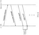
- FIG. 3illustrates a frame format 310 and the corresponding power consumption 360 of an example RF front end, such as RF front end 212 a , during reception of the illustrated frame format.
- the frame format 310is a TDM format in which time is divided into transmission time intervals (TTIs). Control signals and data signals are time division multiplexed within a TTI.
- FIG. 3illustrates an example sequence of transmitted signals within this frame format 310 .
- a TTImay refer to the duration of a transmission on the radio link.
- a TTImay be related to the size of the data blocks passed from the higher network layers to the radio link layer.
- the duration of data symbolssuch as OFDM symbols, is fixed, and there are a predetermined number of data symbol periods during each TTI.
- each TTImay be any number of symbol periods, such as 8, 10, or 12 symbol periods, as examples.
- a downlink control signalmay include information for a UE related to establishing, maintaining, or ending a data session.
- a downlink control signal in a TTImay provide information to a UE about whether a downlink data signal follows in the TTI, and, if so, the control signal may indicate a bandwidth of the data signal.
- the frame format 310is designed with a purpose of reducing power consumption in UE receivers.
- a control signal 315is transmitted at the beginning of each TTI.
- the control signaluses a relatively narrow bandwidth as compared to data signals.
- the bandwidth of control signalsis sufficient to convey control information to intended UE(s), and it is not necessary to use the larger bandwidths used for data signals for the relatively small amount of control information.
- the control signalindicates whether there is a data signal following the control signal.
- the bandwidth used for data signalsis variable, in which case the control signal also indicates the bandwidth used for the data signal that follows.
- data signalsalways occupy a certain bandwidth (such as the entire bandwidth), in which case the bandwidth of the data signal is understood or implied and there is no need for the control signal to convey bandwidth information.
- Each of the transmitted signalsis transmitted using a single carrier frequency f c .
- a single carriersimplifies receivers as compared to systems that use carrier aggregation.
- Carrier aggregationtypically requires the use of multiple LOs, whereas the signaling schemes described herein can use only one LO.
- the approaches described in the present disclosurecan also be applied to multiple carrier frequencies.
- the frame formats disclosed hereinmay apply regardless of the number of antennas employed in the transmitting entity or the receiving entity.
- the signalis transmitted from the transmitting antenna and received at the receive antenna.
- the illustrated frame formatsare transmitted from at least one antenna. Each antenna from among a plurality of antennas may transmit the same or a different pilot structure.
- the illustrated frame format 310will be received by a receive antenna, and may be part of a composite signal that is a sum of signals from a plurality of antennas.
- the control signal 315indicates to the designated UE that no data follows in the TTI.
- Adjustable receiver 200can be used to receive the control signal 315 .
- RF front-end components 215 , 225 , and 230can be temporarily turned off or shut down by the control processor 255 , placing the adjustable receiver 200 in a state of “microsleep.”
- a switchcan be placed between a component, such as an amplifier 215 , an analog filter 225 , and/or an ADC 230 , and its power supply, with the switch being opened for a period of time to shut down power to the component.
- Another example of “microsleep”is placing a component in an idle state in which it receives a reduced amount of power to operate in a reduced capacity.
- the RF power consumption 360 of an RF front endis illustrated in FIG. 3 during reception of various signals.
- the power consumptionis represented by 365 .
- the adjustable receiver 200transitions to a state of microsleep, and the power consumption during that transition is represented by 370 .
- the decrease in power consumptionis represented as a linear decrease over time, but the actual decrease in power consumption may be non-linear but decreasing over time nonetheless.
- the RF power consumptionis much lower than when a signal is being received because amplifiers 215 , analog filters 225 , and ADCs 230 have been shut down.
- the control processor 255informs the amplifiers 215 , analog filters 225 , and ADCs 230 to power on prior to receiving control signal 315 during TTI n+1 .
- the power consumption during that transitionis represented by 375
- the power consumption during reception of the control signal 315 in TTI n+1is represented by 380 .
- the components in receiver 200 that have been shut downneed a period of time to power up sufficiently to receive a signal.
- control signal 315is followed by data signal 325 in TTI n+1 .
- the baseband processor 245demodulates the control signal 315 and provides control signal information to the control processor 255 .
- the information in the control signal 315indicates to the control processor 255 that a data signal will follow.
- the data signal 325is a wider bandwidth than the control signal 315 .
- control processor 255informs amplifiers 215 , analog filters 225 , and ADCs 230 to adjust appropriately for the wider bandwidth. That is, the bandwidths of the amplifiers 215 and analog filters 225 are increased, and the sampling rate of the ADCs 230 is also increased.
- the control processor 255also informs baseband processor 245 to adapt accordingly to the increased bandwidth. For example, for demodulation of OFDM signals, the control processor 255 informs the baseband processor 245 to adjust FFT size or other parameters appropriately in order to demodulate the incoming data signal.
- the frame format 310may further provide for frequency division multiplexing (FDM) among users.
- FDMfrequency division multiplexing
- the data signal 325 of bandwidth Bmay be partitioned in the frequency domain with different portions of the bandwidth B allocated to different users.
- the RF front end 212 for a usermay still be adjusted appropriately for the bandwidth B with extraction and demodulation of the desired portion being performed digitally in the frequency domain using OFDM techniques.
- control signal 315indicates not only that data will follow but also indicates the bandwidth of the data signal 325 .
- control processor 255determines the bandwidth.
- the data signal 325always occupies the same bandwidth, such as the entire available bandwidth, in which case the data signal bandwidth may be understood to be a certain value and there may be no need to include an indication in the control signal. If the bandwidth of the data signals is allowed to vary, components of the adjustable receiver 200 are adjusted from data signal to data signal to receive using just enough bandwidth sufficient to cover the bandwidth of the data signal of interest, instead of always tuning to receive using the entire available system bandwidth.
- transition period 320between the control channel 315 and the data signal 325 to allow the adjustable receiver 200 to adjust to the different bandwidth.
- the transition period 320may be referred to as a switching interval because the receiver 200 is switching from one bandwidth to another.
- the switching intervalmay be quantized to an integer number of symbol periods, such as OFDM symbol periods.
- the power consumption during this transition period 320is represented by 385
- the power consumption during reception of the data signal 325is represented by 390 .
- transition period 330between the data signal 325 and the next control signal 315 in TTI n+2 .
- the transition period 330allows the adjustable receiver 200 time to transition to a smaller bandwidth for control signal 315 .
- the power consumed during the transition period 330is represented by 395 .
- Some conventional TDM systemstypically do not include the transition periods 320 and 330 to allow a receiver to adjust.
- the control signalis transmitted using the same bandwidth as the data signal so receivers do not need to transition between different bandwidths.
- the power consumed during transition periods 320 and 330represent a power penalty for the signaling scheme in FIG. 3 as compared to some conventional systems.
- the power savingincludes the difference in power between the RF power consumed during reception of the data signal and the RF power consumed during reception of the control signal.
- the corresponding energy savingsis computed as an area under the power curves. Under some conditions, the total energy saving exceeds the energy penalty, in which case the frame format and corresponding adjustable receiver 200 extends battery life as compared to conventional TDM systems.
- FIG. 4is a flowchart illustrating an exemplary method 400 for receiving control and data signals.
- the method 400may be implemented in the adjustable receiver 200 , and the method 400 is described with reference to the adjustable receiver 200 .
- the signals that are received in method 400are transmitted by a base station 110 or other type of access point.
- Instructions or codemay be stored in the memory 250 that are executable by the control processor 255 in the adjustable receiver 200 of FIG. 2 to implement the method 400 .
- the method 400begins in block 410 .
- a narrowband control signalis received and processed by the adjustable receiver 200 .
- the control signalis referred to as a narrowband control signal because its bandwidth is typically lower than the data signals, as illustrated in the signaling scheme in FIG. 3 .
- a decisionis made whether a data signal follows the control signal in the current TTI. The control signal will contain this information, and the control signal is demodulated to extract this information.
- the methodproceeds to block 440 , in which the power provided to certain RF front-end components, such as amplifiers 215 , analog filters 225 , and/or ADCs 230 , is reduced to place the components in a microsleep state.
- the control processor 255may send signals to the components in the receiver 200 to control their status as described earlier.
- the componentsare directed to power up or “wake up” to prepare to receive another control signal in block 410 .
- the receiver 200may wait until just before the beginning of the next TTI to request for the RF front-end components to wake up.
- an RF front end 212 a of the receiver 200is adjusted to receive the data signal.
- the control signalmay contain information about the expected bandwidth of the data signal. Alternatively, the bandwidth of the data signal may be understood to be a certain value. In either case, the RF front end is adjusted.
- the control processor 255controls the adjustment.
- the baseband processor 245may also be adjusted.
- a control signalis transmitted at the beginning of each TTI and no further control signals are transmitted within each TTI.
- at least one additional control signalis transmitted in each TTI. For example, there may be a control signal at the beginning of a TTI and another control signal in the middle of the TTI.
- FIG. 5illustrates another frame format 510 and the power consumption of an RF front end 560 during reception of the illustrated frame format.
- the frame format 510is a TDM format in which time is divided into transmission time intervals (TTIs) and control signals and data signals are time division multiplexed.
- TTIstransmission time intervals
- FIG. 5illustrates a transmitted signal sequence within this frame format 510 .
- the transmitted signal sequence in the frame format 510is different than the frame format 310 in that if a data signal is transmitted, the next control signal is transmitted using the bandwidth as the data signal so that there is no switching time or switching interval for adjusting an RF front end. Since there is no need to adjust the RF front end, a data signal can be transmitted until the TTI boundary.
- the signaling formattrades off the potential for energy savings with a more narrowband control signal against the benefit of being able to eliminate dead time for signaling due to switching.
- the signaling schemeuses both narrowband and wideband control signals, depending on whether the control signal follows a data signal.
- FIG. 6is a flowchart illustrating an exemplary method 600 for receiving control and data signals.
- blocks 410 - 425 , 440 , and 445are the same as the corresponding blocks in FIG. 4 .
- a wideband control signalis received.
- the control signalmay be referred to as a wideband control signal because the bandwidth is the same as the previously received data signal, and data signal bandwidth is typically larger than the narrowband control signal bandwidth.
- the control signal 515 in the frame format 510 in FIG. 5is an example narrowband control signal
- the control signal 530is an example wideband control signal.
- the narrowband control signal 515is followed by a transition period 520 to allow an RF front end to adjust to receive the data signal 525 . There is no transition period needed between the data signal 525 and the control signal 530 because the bandwidths are the same.
- the frame format 510may further provide for FDM among users.
- the data signal 525 of bandwidth Bmay be partitioned in the frequency domain with different portions of the bandwidth B allocated to different users.
- the control signal 530may be partitioned similarly.
- the RF front end 212 for a usermay still be adjusted appropriately for the bandwidth B with extraction and demodulation of the desired portion being performed digitally in the frequency domain using OFDM techniques.
- the method 600proceeds to block 440 .
- the power provided to certain RF front end componentssuch as amplifiers 215 , analog filters 225 , and/or ADCs 230 , is reduced to place the components in a microsleep state.
- the componentsare directed to power up or “wake up” to prepare to receive another control signal in block 410 .
- the receiver 200may wait until just before the beginning of the next TTI to request for the RF front-end components to wake up. As part of the wake up process, the bandwidth and sampling rate(s) of the RF front end are set to receive a narrowband control signal.
- Instructions or codemay be stored in the memory 250 of the adjustable receiver 200 that are executable by the control processor 255 to implement the method 600 .
- FIG. 7illustrates an example frame and signal structure for an FDM system.
- the carrier frequency for data designated for a given UEis not fixed and can vary.
- the total system bandwidthcan be divided up into a plurality of frequency bands such that data signals for different UEs can be transmitted simultaneously in different frequency bands.
- the data signal for UE 1 710 and the data signal for UE 2 720overlap in time during TTI 1 but do not overlap in frequency.
- a carrier signal at the center frequency of each of the data signals illustrated in FIG. 7is used to transmit the various data signals.
- the bandwidth allocated for data signals for a given UEcan vary over time, as illustrated by comparing data signals 710 and 730 addressed to UE 1 , for example.
- a base stationmay decide to vary the bandwidth for a particular UE due to variations in amount of data available for transmission versus time, for example.
- Some conventional FDM schemestransmit OFDM signals using the full available bandwidth for downlink transmissions, with different groups of subcarriers within the full signal allocated to different UEs. As a consequence, each UE typically processes the entire bandwidth to extract the group(s) of subcarriers allocated to the UE. In comparison, when the RF carrier frequency is allowed to vary from transmission to transmission, each UE is notified of what RF carrier is being used for its signals. However, the benefit of the approach with multiple RF carriers is the bandwidth can be used more efficiently if data signals are allowed to use different RF carriers so that each UE does not have to process the entire bandwidth and can use the RF carrier devoted to it.
- FIG. 8is a protocol diagram illustrating the signaling aspects between a UE 120 and a base station 110 to support FDM with variable bandwidths.
- control signalsare transmitted via a different channel from data signals.
- the control channelmay be in a different frequency band or in a different time slot, as an example.
- a control signalindicates the center frequency (if center frequency is dynamic) and the bandwidth of an associated data signal.
- the data signalis then sent using the designated bandwidth and center frequency.
- the receiver of the UE 120is tuned to the data signal bandwidth. This process is repeated as long as there is data to convey between base station 110 and UE 120 .
- the base station 110may coordinate this process across different UEs 120 to efficiently utilize the available spectral bandwidth.
- This coordinated processwas described with respect to FIG. 7 .
- FIG. 9is a protocol diagram illustrating the signaling aspects between a UE 120 and a base station 110 to support variable bandwidth signaling.
- the UE 120transmits a capability message to the base station 110 .
- the capability messagemay provide one or more indications corresponding to a number of parameters and capabilities of the UE 110 .
- the capability messagemay include an indication whether the UE 110 is capable of dynamically switching between signals of various bandwidths.
- the capability messagemay further include an indication of switching latency for the UE 120 , so that the base station 110 can respond by inserting or reserving a time interval between control and data signals to allow the UE 120 to adjust its RF front end. The time interval accommodates the switching latency indicated by a UE.
- the base station 110transmits a response message in response to the capability message.
- the response messagemay provide one or more indications corresponding to a number of parameters and capabilities.
- the response messagemay indicate that dynamic bandwidth switching is activated.
- Dynamic bandwidth switchingmay be activated or deactivated as frequently as desired during a connection.
- messages indicating that dynamic bandwidth switching is activated or deactivatedmay be transmitted by the base station 110 as frequently as desired.
- the response messagemay also indicate the time offset between a control signal and the corresponding data signal in a TTI.
- the time offsetmay be based on the switching latency indicated in the capability message. The time offset would accommodate the latency needed to decode the control signal and allow the RF front end to switch bandwidths.
- the response messagemay also indicate whether the bandwidth is maintained at a wide bandwidth of the data signal for the next control signal, as illustrated in FIG. 5 , or returns to a narrow bandwidth, as illustrated in FIG. 3 .
- a previous control signalmay also indicate whether the bandwidth is maintained at a wide bandwidth of the data signal for a next control signal, as illustrated in FIG. 5 , or returns to a narrow bandwidth, as illustrated in FIG. 3 .
- the base station 110may decide not to activate dynamic bandwidth switching. If dynamic bandwidth switching is not activated, the control signals occupy the same bandwidth as data signals and there is no time offset between control signals and data signals.
- control and data informationcan proceed as needed.
- a control signalis transmitted by the base station 120 and received by the UE 110 .
- the UE 110adjusts its RF front end, and then a data signal is transmitted by the base station 120 and received by the UE 110 .
- FIG. 10is a block diagram of a transceiver 900 that implements aspects of this disclosure.
- the transceiver 900comprises antennas 210 , baseband processor 245 , memory 250 , and controller/processor 255 as described previously.
- the transceiverfurther includes RF receive (Rx) front ends 910 .
- Each RF Rx front end 910may include an amplifier, an analog filter, and an ADC as described with respect to FIG. 2 .
- Other RF Rx front end architecturesare compatible with this disclosure. For example, some RF Rx front end architectures perform most processing in the analog domain, and some RF Rx front end architectures perform most processing in the digital domain. Furthermore, some RF Rx front end architectures perform most processing at an intermediate frequency (IF), rather than baseband. These RF Rx front ends can be made adjustable to accommodate differences in control signal and data signal bandwidths.
- IFintermediate frequency
- the transceiverfurther includes RF transmit (Tx) front ends 920 .
- Each RF Tx front end 920accepts a stream of digital data symbols from baseband processor and converts the digital data symbols to an analog signal for transmission over the corresponding antenna 210 .
- the transceiver 900is suitable for either a base station 110 or a UE 120 .
- the RF Tx front ends 920are engaged, and the controller/processor 255 controls the RF Tx front ends 920 as well as baseband processor 245 to generate signals of various bandwidths.
- the combination of RF Tx front end 920 and baseband processor 245is an example of a transmitter.
- the combination of RF Rx front end 910 and baseband processor 245is an example of a receiver.
- An RF Rx front end 910may comprise the RF front end 212 described previously.
- baseband process 245may additionally be configured to modulate OFDM symbols. Modulation of OFDM symbols is well known in the art and in some embodiments an inverse FFT (IFFT) is performed to convert frequency domain data to the time domain. As described earlier, there are various techniques for changing bandwidths of OFDM signals. One technique involves varying the number of subcarriers used for generating OFDM signals.
- Information and signalsmay be represented using any of a variety of different technologies and techniques.
- data, instructions, commands, information, signals, bits, symbols, and chipsthat may be referenced throughout the above description may be represented by voltages, currents, electromagnetic waves, magnetic fields or particles, optical fields or particles, or any combination thereof.
- FIG. 11illustrates another frame format 1110 .
- the frame formatis a TDM format in which time is divided into TTIs and control signals and data signals are time multiplexed.
- FIG. 11illustrates a transmitted signal sequence within this frame format 1110 .
- the control signals 1115are narrowband control signals.
- a base stationallows one full TTI duration for bandwidth switching delay of a receiver.
- the control signal 1115 in TTI nhas a bandwidth switch indicator to trigger widening of RF front end bandwidth to receive wider bandwidth data in TTI n+1 .
- the control signal 1115 in TTI n+1indicates what frequency range is allocated for data in TTI n+1 .
- data radio block allocation 1125 in TTI n+1is allocated or prescheduled using control signal 1115 in TTI n .
- control signal 1115 in TTI n+2indicates the use of data resources 1135 and 1145 in TTI n+2 .
- An advantage of the first optionis that the scheduler in a base station only needs to know that the UE will be scheduled in the next TTI to set the indicator. The base station scheduler does not need to do the prescheduling and avoids a corresponding increase in complexity.
- An advantage of the second optionis there is a saving of a control channel resource in that there is no bandwidth switch indicator.
- the receiver bandwidth envelopeis indicated in FIG. 11 .
- the receiver bandwidth enveloperepresents the frequency range versus time utilized by a receiver, such as adjustable receiver 200 , in the frame format of interest.
- the receiver bandwidthmay transition from a relatively narrow bandwidth for reception of control signal 1115 to a relatively wide bandwidth (in this embodiment, the full system bandwidth or full bandwidth available for data) for reception of data.
- the receiver bandwidthmay transition from a relatively wide bandwidth to a relatively narrow bandwidth as shown.
- FIG. 12illustrates another frame format 1210 .
- a data signalmay be allocated for only a latter fraction or portion of a TTI, such that there is enough time for the receiver bandwidth to transition from a narrow bandwidth to receive a control signal to a wider bandwidth to receive a data signal.
- the control signal 1215may indicate that there will be a data signal 1225 later in the TTI.
- a smaller duration of a TTI than the example in FIG. 11may be available for receiver bandwidth switching.
- the receiver bandwidthis increased.
- One such example increase of receiveris illustrated by the receiver bandwidth envelope in FIG. 12 .
- control signal 1215 in TTI n+1may indicate the bandwidths of data signals 1235 and 1245 .
- Control signals that are transmitted after the receiver has transmitted to a higher bandwidthmay be referred to as wideband control signals, and in some embodiments a wideband control signal refers to a control signal and one or more data signals that are transmitted simultaneously in different frequency bands (i.e., frequency division multiplexed).
- An example of a wideband control signalis control signal 1215 in TTI n+1 in FIG. 12 , and this control signal is frequency division multiplexed with data signals 1235 and 1245 .
- the transmitted signalincludes a control signal portion and a data signal portion.
- FIG. 12also illustrates a countdown mechanism for returning a receiver to a narrow band for reception of control signals.
- control signal 1215indicates there is no data within TTI n+c .
- TTI n+2is a candidate for returning the receiver bandwidth to a narrow bandwidth using mechanisms described previously—for example with respect to FIG. 2 .
- a countdown mechanismis used.
- a counteris set to a maximum value, such as four, three, two, one or any integer value. In the embodiment in FIG. 12 , the maximum value is one. The counter is decremented each successive consecutive TTI that does not contain data.
- the counteris reset to the maximum value.
- the counteris decremented to zero.
- a counter value of zeroindicates that the receiver should thereafter reduce its bandwidth. For example, in TTI n+3 , the receiver reduces its bandwidth as shown (the receiver envelope transitions from a wide bandwidth to a narrow bandwidth during transition period 1230 ).
- An alternative to the countdown timeris that the receiver bandwidth is reduced to a narrow bandwidth in the first TTI that does not contain data.
- FIG. 13illustrates another frame format 1310 .
- Frame format 1310is similar to frame format 1110 , except that for frame format 1310 , an embodiment of a receiver is enhanced with bandwidth adaptation according to the data allocation. For example, in FIG. 11 during TTI n+1 the receiver bandwidth is set to the system bandwidth or the maximum supported data bandwidth, whereas in FIG. 13 the receiver bandwidth during TTI n+1 is set just large enough to receive data signal 1325 while remaining symmetric about center frequency f c .
- control signal 1115 in TTI nhas a bandwidth switch indicator plus bandwidth information to trigger widening of RF front end bandwidth to be just wide enough to receive wider bandwidth data in TTI n+1 .
- data radio block allocation 1125 in TTI n+1is allocated or prescheduled using control signal 1115 in TTI n .
- control signal 1115 in TTI n+4indicates the use of data resources 1335 in TTI n+4 .
- control signals 1115 in TTI n+2 and TTI n+3indicate that there is no data in the respective TTIs, so the receiver bandwidth remains narrow and the receiver can transition to a state of microsleep.
- FIG. 14illustrates another frame format 1410 .
- this frame format 1410When this frame format 1410 is used the center frequency may not remain the same independent of TTI.
- This frame formatfacilitates use of a receiver that can vary its center frequency and RF front end bandwidth. The receiver bandwidth envelope is indicated.
- the bandwidth of a receiveris centered on a frequency at the center of control signal 1415 in TTI n and then the center is shifted during transition period 1420 to the frequency at the center of data signal 1445 .
- This frame format 1410 combined with prescheduling of data signals 1445 , 1455 , and 1465 using control signal 1415implies that the control signals 1425 may be ignored by a receiver configured to receive data signals 1445 , 1455 and 1465 .
- prescheduling fractional TTIs for data signalsmay be performed.
- data signals 1445 and 1465occupy a fraction of a TTI time interval, and the duration of the data signals may be indicated by control signal 1415 .
- the RF front endmay be re-tuned to a bandwidth for control signal 1435 during transition period 1430 .
- FIG. 15illustrates another frame format 1510 .
- the frame format 1510is an example TDM format in which control signals and data signals are received by a UE, and acknowledgement messages (ACKs) are transmitted by the UE in response to reception of data signals.
- ACKacknowledgement messages
- an ACKis used to indicate whether all or part of a preceding data signal was received correctly.
- the RF front end bandwidth of a receiveris maintained at the system bandwidth or maximum available data bandwidth until a TTI is received that does not have a data allocation.
- control signal 1535indicates that there is no data in the TTI so a receiver can reduce its bandwidth during transition period 1530 as shown.
- Guard periodsmay be inserted on either side of an ACK.
- guard periods 1544 and 1546are inserted on either side of ACK 1445 .
- Control signal 1515 in TTI nmay be used to schedule data signal 1565 for a fraction of the TTI. After receiving control signal 1515 a receiver transitions its RF front end bandwidth to receive data signal 1565 as shown. Alternatively (not illustrated), control signal 1515 in TTI n could carry bandwidth switch indicator or prescheduling information, similar to the scheme described in FIG. 11 , and data allocation is deferred until TTI n+1 . This scheme avoids allocation of data RBs for only a fraction of TTI (as in 1565 ), at the expense of delayed start for the data transfer.
- Narrowband control signal 1525indicates that data signal 1575 is present, so the receiver is configured to receive the data signal.
- the control signal 1525may use a subset of the available subcarriers, and the portion of the data signal 1575 that is simultaneous with the control signal 1525 may occupy the remaining available subcarriers.
- Control signal 1535indicates that there is no data in TTI n+2 , so the receiver reduces its RF front end bandwidth and may also transition to a microsleep state during the transition period 1530 .
- Some advantages of the frame format 1510include the following. First, for consecutive TTI data allocation, once the overhead is paid for RF bandwidth widening (causing delayed start of data radio blocks), in the subsequent TTI there is no data radio block overhead. Second, enhancements for wideband-to-narrowband transitions, such as a countdown timer or bandwidth switch indicator described with respect to FIG. 12 , could also be applied.
- FIG. 16illustrates another frame format 1610 .
- the frame format 1610is an example TDM format in which control signals and data signals are received by a UE, and ACKs are transmitted by the UE in response to reception of data signals.
- An example embodiment of scheduling data signals according to frame format 1610is as follows. Control signal 1615 in TTI n may be used to schedule data signal 1620 for a fraction of the TTI. After receiving control signal 1615 a receiver transitions its RF front end bandwidth to receive data signal 1620 as shown. The receiver switches back to a narrowband bandwidth for reception of each control signal as shown. For example, the receiver transitions to a narrow bandwidth during transition period 1640 and then receives control signal 1625 using a narrow bandwidth as shown.
- An advantage of the frame format 1610may include that bandwidth switching behavior is the same across TTIs.
- FIGS. 3 and 5can be implemented using the adjustable receiver 200 as described previously, it is readily understood that the frame formats in FIGS. 11-16 can be implemented in a straightforward manner using the adjustable receiver 200 .
- a general-purpose processormay be a microprocessor, but in the alternative, the processor may be any conventional processor, controller, microcontroller, or state machine.
- a processormay also be implemented as a combination of computing devices (e.g., a combination of a DSP and a microprocessor, multiple microprocessors, one or more microprocessors in conjunction with a DSP core, or any other such configuration).
- the functions described hereinmay be implemented in hardware, software executed by a processor, firmware, or any combination thereof. If implemented in software executed by a processor, the functions may be stored on or transmitted over as one or more instructions or code on a computer-readable medium. Other examples and implementations are within the scope of the disclosure and appended claims. For example, due to the nature of software, functions described above can be implemented using software executed by a processor, hardware, firmware, hardwiring, or combinations of any of these. Features implementing functions may also be physically located at various positions, including being distributed such that portions of functions are implemented at different physical locations.
- “or” as used in a list of itemsindicates an inclusive list such that, for example, a list of [at least one of A, B, or C] means A or B or C or AB or AC or BC or ABC (i.e., A and B and C).
Landscapes
- Engineering & Computer Science (AREA)
- Signal Processing (AREA)
- Computer Networks & Wireless Communication (AREA)
- Quality & Reliability (AREA)
- Databases & Information Systems (AREA)
- Mobile Radio Communication Systems (AREA)
- Circuits Of Receivers In General (AREA)
- Communication Control (AREA)
- Transceivers (AREA)
- Telephonic Communication Services (AREA)
Abstract
Description
Claims (53)
Priority Applications (2)
| Application Number | Priority Date | Filing Date | Title |
|---|---|---|---|
| US16/186,297US11224015B2 (en) | 2014-10-31 | 2018-11-09 | Dynamic bandwidth switching for reducing power consumption in wireless communication devices |
| US17/545,832US11711762B2 (en) | 2014-10-31 | 2021-12-08 | Dynamic bandwidth switching for reducing power consumption in wireless communication devices |
Applications Claiming Priority (5)
| Application Number | Priority Date | Filing Date | Title |
|---|---|---|---|
| US201462073603P | 2014-10-31 | 2014-10-31 | |
| US14/846,051US9572106B2 (en) | 2014-10-31 | 2015-09-04 | Dynamic bandwidth switching for reducing power consumption in wireless communication devices |
| US15/393,736US9756563B2 (en) | 2014-10-31 | 2016-12-29 | Dynamic bandwidth switching for reducing power consumption in wireless communication devices |
| US15/617,960US10154456B2 (en) | 2014-10-31 | 2017-06-08 | Dynamic bandwidth switching for reducing power consumption in wireless communication devices |
| US16/186,297US11224015B2 (en) | 2014-10-31 | 2018-11-09 | Dynamic bandwidth switching for reducing power consumption in wireless communication devices |
Related Parent Applications (1)
| Application Number | Title | Priority Date | Filing Date |
|---|---|---|---|
| US15/617,960ContinuationUS10154456B2 (en) | 2014-10-31 | 2017-06-08 | Dynamic bandwidth switching for reducing power consumption in wireless communication devices |
Related Child Applications (1)
| Application Number | Title | Priority Date | Filing Date |
|---|---|---|---|
| US17/545,832ContinuationUS11711762B2 (en) | 2014-10-31 | 2021-12-08 | Dynamic bandwidth switching for reducing power consumption in wireless communication devices |
Publications (2)
| Publication Number | Publication Date |
|---|---|
| US20190082388A1 US20190082388A1 (en) | 2019-03-14 |
| US11224015B2true US11224015B2 (en) | 2022-01-11 |
Family
ID=55854282
Family Applications (5)
| Application Number | Title | Priority Date | Filing Date |
|---|---|---|---|
| US14/846,051ActiveUS9572106B2 (en) | 2014-10-31 | 2015-09-04 | Dynamic bandwidth switching for reducing power consumption in wireless communication devices |
| US15/393,736ActiveUS9756563B2 (en) | 2014-10-31 | 2016-12-29 | Dynamic bandwidth switching for reducing power consumption in wireless communication devices |
| US15/617,960ActiveUS10154456B2 (en) | 2014-10-31 | 2017-06-08 | Dynamic bandwidth switching for reducing power consumption in wireless communication devices |
| US16/186,297ActiveUS11224015B2 (en) | 2014-10-31 | 2018-11-09 | Dynamic bandwidth switching for reducing power consumption in wireless communication devices |
| US17/545,832ActiveUS11711762B2 (en) | 2014-10-31 | 2021-12-08 | Dynamic bandwidth switching for reducing power consumption in wireless communication devices |
Family Applications Before (3)
| Application Number | Title | Priority Date | Filing Date |
|---|---|---|---|
| US14/846,051ActiveUS9572106B2 (en) | 2014-10-31 | 2015-09-04 | Dynamic bandwidth switching for reducing power consumption in wireless communication devices |
| US15/393,736ActiveUS9756563B2 (en) | 2014-10-31 | 2016-12-29 | Dynamic bandwidth switching for reducing power consumption in wireless communication devices |
| US15/617,960ActiveUS10154456B2 (en) | 2014-10-31 | 2017-06-08 | Dynamic bandwidth switching for reducing power consumption in wireless communication devices |
Family Applications After (1)
| Application Number | Title | Priority Date | Filing Date |
|---|---|---|---|
| US17/545,832ActiveUS11711762B2 (en) | 2014-10-31 | 2021-12-08 | Dynamic bandwidth switching for reducing power consumption in wireless communication devices |
Country Status (24)
| Country | Link |
|---|---|
| US (5) | US9572106B2 (en) |
| EP (4) | EP4496257A3 (en) |
| JP (2) | JP6629851B2 (en) |
| KR (3) | KR102416055B1 (en) |
| CN (2) | CN107113722B (en) |
| AR (1) | AR104472A1 (en) |
| AU (1) | AU2015339910B2 (en) |
| CA (1) | CA2962741C (en) |
| CL (2) | CL2017001032A1 (en) |
| CO (1) | CO2017004048A2 (en) |
| DK (1) | DK3213562T3 (en) |
| ES (2) | ES2858406T3 (en) |
| HU (2) | HUE053471T2 (en) |
| MX (1) | MX368489B (en) |
| MY (1) | MY195344A (en) |
| NZ (1) | NZ730381A (en) |
| PH (1) | PH12017500535A1 (en) |
| RU (1) | RU2690172C2 (en) |
| SA (1) | SA517381399B1 (en) |
| SG (1) | SG11201702098RA (en) |
| SI (1) | SI3213562T1 (en) |
| TW (2) | TWI678119B (en) |
| WO (1) | WO2016069115A1 (en) |
| ZA (1) | ZA201703010B (en) |
Families Citing this family (44)
| Publication number | Priority date | Publication date | Assignee | Title |
|---|---|---|---|---|
| US9572106B2 (en) | 2014-10-31 | 2017-02-14 | Qualcomm Incorporated | Dynamic bandwidth switching for reducing power consumption in wireless communication devices |
| US9877278B2 (en)* | 2015-04-10 | 2018-01-23 | Futurewei Technologies, Inc. | Monitoring a narrowband control channel for a wideband system to reduce power consumption |
| US10681633B2 (en)* | 2016-04-05 | 2020-06-09 | Qualcomm Incorporated | Configurable subframe structures in wireless communication |
| US10299260B2 (en) | 2016-05-20 | 2019-05-21 | Qualcomm Incorporated | Methods and apparatus for flexible bandwidth operation |
| US10728852B2 (en) | 2016-07-18 | 2020-07-28 | Qualcomm Incorporated | Efficient power utilization for enhanced component carriers |
| JP6911296B2 (en)* | 2016-08-08 | 2021-07-28 | ソニーグループ株式会社 | Communication equipment, communication methods, and programs |
| US20180049067A1 (en)* | 2016-08-12 | 2018-02-15 | Qualcomm Incorporated | Techniques for enabling flexible guard-bands for a radio access technology in new radio |
| US10003482B2 (en)* | 2016-08-31 | 2018-06-19 | Silicon Laboratories Inc. | Receiver architecture having full-band capture and narrow-band paths |
| US10973026B2 (en)* | 2016-09-09 | 2021-04-06 | Blackberry Limited | Transitioning between wideband and narrowband communications |
| EP3301846A1 (en)* | 2016-09-30 | 2018-04-04 | Nokia Technologies OY | Method, system and apparatus |
| WO2018066923A1 (en)* | 2016-10-07 | 2018-04-12 | Lg Electronics Inc. | Method and apparatus for supporting energy saving mechanisms for nr in wireless communication system |
| CN117221960A (en)* | 2016-10-10 | 2023-12-12 | 瑞典爱立信有限公司 | Method and apparatus for using adaptive bandwidth in a wireless communication network |
| ES2928109T3 (en)* | 2016-10-26 | 2022-11-15 | Huawei Tech Co Ltd | Variable bandwidth based communication method and device |
| ES2870040T3 (en)* | 2016-11-03 | 2021-10-26 | Ericsson Telefon Ab L M | Search Space Variable Subband Settings |
| US10312953B2 (en) | 2016-12-26 | 2019-06-04 | Industrial Technology Research Institute | Orthogonal frequency division multiplexing receiver with low-resolution analog to digital converter and electronic device thereof |
| US20190349915A1 (en) | 2017-01-03 | 2019-11-14 | Lg Electronics Inc. | Method for transmitting/receiving signals by using beams in wireless communication system, and device for same |
| WO2018126453A1 (en)* | 2017-01-06 | 2018-07-12 | 广东欧珀移动通信有限公司 | Handover method, base station, and terminal |
| WO2018126454A1 (en)* | 2017-01-06 | 2018-07-12 | 广东欧珀移动通信有限公司 | Service transmission method, base station, and terminal |
| CN116567826A (en)* | 2017-01-11 | 2023-08-08 | 联发科技股份有限公司 | Method for wireless communication and user equipment |
| EP3577825B1 (en)* | 2017-02-02 | 2021-06-30 | Telefonaktiebolaget LM Ericsson (Publ) | Apparatuses and methods of switching between different numerologies |
| US10856310B2 (en)* | 2017-02-03 | 2020-12-01 | Qualcomm Incorporated | Retuning in machine type communications |
| WO2018144892A1 (en)* | 2017-02-03 | 2018-08-09 | Intel IP Corporation | Provisions facilitating bandwidth adaptation transition and measurement |
| JP2018133733A (en)* | 2017-02-16 | 2018-08-23 | 株式会社フジクラ | Wireless communication system and wireless communication method |
| CN111107643B (en)* | 2017-06-16 | 2021-04-09 | 华为技术有限公司 | Bandwidth resource allocation method, device and system |
| US10687352B2 (en)* | 2017-06-23 | 2020-06-16 | Qualcomm Incorporated | Multiplexing clustered control information and data |
| CN109275190B (en)* | 2017-07-17 | 2021-10-26 | 华为技术有限公司 | Communication method and device |
| WO2019061080A1 (en) | 2017-09-27 | 2019-04-04 | Oppo广东移动通信有限公司 | Bandwidth part switching method, terminal device, and computer storage medium |
| CN109586881B (en) | 2017-09-29 | 2021-11-12 | 株式会社Kt | Method and apparatus for switching bandwidth parts in a new radio |
| US10594468B2 (en)* | 2017-09-29 | 2020-03-17 | Mediatek Inc. | Efficient bandwidth adaptation for a wideband carrier |
| KR102156695B1 (en)* | 2017-09-29 | 2020-09-17 | 주식회사 케이티 | Method for switching bandwidth part in new radio and Apparatuses thereof |
| KR102515981B1 (en) | 2017-10-11 | 2023-03-30 | 삼성전자 주식회사 | Method and apparatus for bandwidth part operation in wirelss communication system |
| TWI674811B (en)* | 2017-11-16 | 2019-10-11 | 財團法人資訊工業策進會 | User equipment and base station for mobile communication system |
| US10869268B2 (en)* | 2018-01-19 | 2020-12-15 | Mediatek Inc. | NR power saving enhancements |
| US10834749B2 (en) | 2018-02-19 | 2020-11-10 | Electronics And Telecommunications Research Institute | Method for bandwidth part management in communication system and apparatus for the same |
| US11272507B2 (en)* | 2018-07-23 | 2022-03-08 | Qualcomm Incorporated | Bandwidth part switching for multiple transceiver nodes |
| CN112771935B (en)* | 2018-10-01 | 2022-05-13 | 华为技术有限公司 | Power saving for wireless communication receivers |
| WO2020142905A1 (en)* | 2019-01-08 | 2020-07-16 | 北京小米移动软件有限公司 | Bandwidth part switching method and apparatus |
| US20220159720A1 (en)* | 2019-05-13 | 2022-05-19 | Nokia Solutions And Networks Oy | Mechanism for transmission for wideband system in unlicensed spectrum |
| JP7393546B2 (en) | 2019-12-02 | 2023-12-06 | テレフオンアクチーボラゲット エルエム エリクソン(パブル) | Wake-up communication in wireless communication systems |
| CN113329495B (en)* | 2020-02-29 | 2022-09-02 | 华为技术有限公司 | Communication method and device |
| US11539393B2 (en)* | 2020-08-07 | 2022-12-27 | Apple Inc. | Radio-frequency front end modules with leakage management engines |
| CN114698075A (en)* | 2020-12-26 | 2022-07-01 | 华为技术有限公司 | Method and device for sending information between WLAN devices |
| EP4203366A1 (en) | 2021-12-22 | 2023-06-28 | Nokia Technologies Oy | Irregular bandwidth support at a user equipment |
| CN119948949A (en)* | 2022-09-24 | 2025-05-06 | 华为技术有限公司 | Method and apparatus for adjusting a configuration for performing conversion between analog and digital signals |
Citations (40)
| Publication number | Priority date | Publication date | Assignee | Title |
|---|---|---|---|---|
| JPH09107580A (en) | 1995-10-12 | 1997-04-22 | Nippon Telegr & Teleph Corp <Ntt> | Radio channel allocation method |
| CO4650152A1 (en) | 1996-08-28 | 1998-09-03 | Ericsson Inc | APPARATUS TO IMPROVE THE LINK MARGIN IN WIRELESS COMMUNICATIONS |
| WO2003001681A2 (en) | 2001-06-25 | 2003-01-03 | Nokia Corporation | Optimization of mcs and multicode with tfci signaling |
| JP2003309533A (en) | 2002-04-17 | 2003-10-31 | Matsushita Electric Ind Co Ltd | Wireless transmitting device, wireless receiving device and method thereof |
| US6999438B2 (en) | 1996-01-18 | 2006-02-14 | Kabushiki Kaisha Toshiba | Radio communication system |
| WO2006046307A1 (en) | 2004-10-29 | 2006-05-04 | Fujitsu Limited | Communication device by multicarrier transmission method and communication system |
| WO2007023809A1 (en) | 2005-08-26 | 2007-03-01 | Matsushita Electric Industrial Co., Ltd. | Scalable bandwidth system, radio base station apparatus and radio terminal apparatus |
| WO2007131558A1 (en) | 2006-05-12 | 2007-11-22 | Panasonic Corporation | Reservation of radio resources for users in a mobile communications system |
| WO2008050428A1 (en) | 2006-10-26 | 2008-05-02 | Fujitsu Limited | Radio base station apparatus, pilot transmitting method thereof and terminal apparatus |
| US7436809B2 (en) | 2004-03-08 | 2008-10-14 | National Institute Of Information And Communications Technology, Incorporated Administrative Agency | Communicating system, communicating method, base station, and mobile station |
| WO2009038429A2 (en) | 2007-09-21 | 2009-03-26 | Lg Electronics Inc. | Method of transmitting a wideband frame |
| US20090122765A1 (en) | 2005-03-04 | 2009-05-14 | Matsushita Electric Industrial Co., Ltd. | Method and apparatus for the synchronisation of the physical layers in heterogeneous mobile communications networks |
| US20100093288A1 (en)* | 2008-10-09 | 2010-04-15 | Qualcomm Incorporated | Method and apparatus for facilitating power conservation via time-gating in a wireless communication system |
| US20110243261A1 (en)* | 2010-03-30 | 2011-10-06 | Infineon Technologies Ag | Communication device |
| WO2011136518A2 (en) | 2010-04-26 | 2011-11-03 | Samsung Electronics Co., Ltd. | Method and apparatus for controlling inter-cell interference of control channels in ofdm-based hierarchical cellular system |
| RU2434365C2 (en) | 2006-12-18 | 2011-11-20 | Самсунг Электроникс Ко., Лтд. | Method and apparatus for transmitting/receiving data and control information over uplink in wireless communication system |
| US8081722B1 (en) | 2008-04-04 | 2011-12-20 | Harris Corporation | Communications system and device using simultaneous wideband and in-band narrowband operation and related method |
| US8184656B2 (en) | 2007-10-02 | 2012-05-22 | Microsoft Corporation | Control channel negotiated intermittent wireless communication |
| US8264996B2 (en) | 2004-09-24 | 2012-09-11 | Microsoft Corporation | Signalling channel and radio system for power saving in wireless devices |
| US20120320896A1 (en) | 2009-12-18 | 2012-12-20 | Electronics And Telecommunications Research Institute | Method for sending/receiving data in a wireless packet communication system in which there is simultaneous communication with various terminals |
| US8369280B2 (en) | 2011-07-01 | 2013-02-05 | Ofinno Techologies, LLC | Control channels in multicarrier OFDM transmission |
| WO2013049768A1 (en) | 2011-09-30 | 2013-04-04 | Interdigital Patent Holdings, Inc. | Device communication using a reduced channel bandwidth |
| WO2013067386A1 (en) | 2011-11-04 | 2013-05-10 | Intel Corporation | Narrow bandwidth device in a broadband network |
| WO2013070714A1 (en) | 2011-11-07 | 2013-05-16 | Qualcomm Incorporated | Signaling and traffic carrier splitting for wireless communications systems |
| WO2013072222A1 (en) | 2011-11-18 | 2013-05-23 | Panasonic Corporation | Active bandwidth indicator for power-saving user equipment |
| EP2007090B1 (en) | 2006-03-17 | 2013-06-19 | Huawei Technologies Co., Ltd. | An integration media gateway device, communication system and the method for switching data |
| US8488700B2 (en) | 2011-07-31 | 2013-07-16 | Broadcom Corporation | Discrete digital receiver with sample memory |
| WO2013106740A2 (en) | 2012-01-11 | 2013-07-18 | Interdigital Patent Holdings, Inc. | Adaptive control channel |
| US20130194995A1 (en) | 2010-10-12 | 2013-08-01 | Telefonaktiebolaget L M Ericsson (Publ) | Micro Sleep Mode Control For a Receiver |
| WO2013116254A1 (en) | 2012-02-01 | 2013-08-08 | Fujitsu Limited | Narrowband decoding by an endpoint |
| US20130230013A1 (en) | 2010-11-25 | 2013-09-05 | Lg Electronics Inc. | Method and apparatus for transmitting a control channel and a data channel in a wireless communication system |
| WO2013155382A1 (en) | 2012-04-13 | 2013-10-17 | Intel Corporation | Evolved node b, user equipment, and method for operation of narrow bandwidth user equipment in wide bandwidth broadband networks |
| US20140016541A1 (en) | 2011-03-25 | 2014-01-16 | Lg Electronics Inc. | Backhaul link subframe structure in mobile communication system and method for transmitting information thereof |
| EP2764745A1 (en) | 2011-10-06 | 2014-08-13 | Samsung Electronics Co., Ltd. | Method and apparatus for operating multi-band and multi-cell |
| US20140286256A1 (en) | 2013-03-25 | 2014-09-25 | Altiostar Networks, Inc. | Systems and methods for scheduling of data packets based on delay tolerance of applications |
| WO2015018616A1 (en) | 2013-08-06 | 2015-02-12 | Sony Corporation | Communications system, infrastructure equipment and method |
| US20160020891A1 (en) | 2014-07-21 | 2016-01-21 | Intel IP Corporation | System and method for tdd communications |
| US20160127991A1 (en) | 2014-10-31 | 2016-05-05 | Qualcomm Incorporated | Dynamic bandwidth switching for reducing power consumption in wireless communication devices |
| WO2016093639A1 (en) | 2014-12-12 | 2016-06-16 | 삼성전자 주식회사 | Method and apparatus for power saving of terminal in wireless lan system |
| EP2580897B1 (en) | 2010-06-11 | 2018-08-08 | Marvell World Trade Ltd. | Method and apparatus for determining channel bandwidth |
Family Cites Families (8)
| Publication number | Priority date | Publication date | Assignee | Title |
|---|---|---|---|---|
| CN100531458C (en)* | 2002-05-13 | 2009-08-19 | 三星电子株式会社 | A method of performing an inter-rat measurement |
| CN101378579B (en)* | 2007-08-30 | 2012-11-14 | 中兴通讯股份有限公司 | Method for assigning multi-bandwidth terminal of OFDM access system |
| CN101807914B (en) | 2009-07-21 | 2011-12-28 | 清华大学 | Frequency self-correction phase lock loop adopting bonding wire as electric inductance of oscillator |
| US8295893B2 (en)* | 2010-09-10 | 2012-10-23 | Motorola Solutions, Inc. | System and method for managing power consumption in a device |
| JP5548634B2 (en) | 2011-02-23 | 2014-07-16 | 株式会社日立製作所 | Dynamic bandwidth control, optical subscriber unit and system for intermittent OLT activation |
| US9622230B2 (en)* | 2012-05-17 | 2017-04-11 | Qualcomm Incorporated | Narrow band partitioning and efficient resource allocation for low cost user equipments |
| GB2508887A (en)* | 2012-12-14 | 2014-06-18 | Sony Corp | A cable modem reduces sampling rate when not detecting payload data |
| KR102071535B1 (en)* | 2013-08-26 | 2020-01-30 | 삼성전자주식회사 | Apparatus and method for allocating resources to switch between macro cell and small cell in wireless communication system |
- 2015
- 2015-09-04USUS14/846,051patent/US9572106B2/enactiveActive
- 2015-09-05CACA2962741Apatent/CA2962741C/enactiveActive
- 2015-09-05DKDK15771324.9Tpatent/DK3213562T3/enactive
- 2015-09-05HUHUE18214151Apatent/HUE053471T2/enunknown
- 2015-09-05KRKR1020217043162Apatent/KR102416055B1/enactiveActive
- 2015-09-05AUAU2015339910Apatent/AU2015339910B2/enactiveActive
- 2015-09-05SISI201530699Tpatent/SI3213562T1/enunknown
- 2015-09-05CNCN201580058119.7Apatent/CN107113722B/enactiveActive
- 2015-09-05SGSG11201702098RApatent/SG11201702098RA/enunknown
- 2015-09-05EPEP24217124.7Apatent/EP4496257A3/enactivePending
- 2015-09-05ESES18214151Tpatent/ES2858406T3/enactiveActive
- 2015-09-05MXMX2017005328Apatent/MX368489B/enactiveIP Right Grant
- 2015-09-05WOPCT/US2015/048738patent/WO2016069115A1/enactiveApplication Filing
- 2015-09-05EPEP18214151.5Apatent/EP3484213B1/enactiveActive
- 2015-09-05NZNZ730381Apatent/NZ730381A/enunknown
- 2015-09-05CNCN202010413840.6Apatent/CN111542103B/enactiveActive
- 2015-09-05ESES15771324Tpatent/ES2732040T3/enactiveActive
- 2015-09-05JPJP2017522615Apatent/JP6629851B2/enactiveActive
- 2015-09-05EPEP20211110.0Apatent/EP3800944A1/enactivePending
- 2015-09-05MYMYPI2017700901Apatent/MY195344A/enunknown
- 2015-09-05EPEP15771324.9Apatent/EP3213562B1/enactiveActive
- 2015-09-05RURU2017114653Apatent/RU2690172C2/enactive
- 2015-09-05KRKR1020227022073Apatent/KR102505145B1/enactiveActive
- 2015-09-05HUHUE15771324patent/HUE044937T2/enunknown
- 2015-09-05KRKR1020177011870Apatent/KR102346769B1/enactiveActive
- 2015-09-15TWTW104130462Apatent/TWI678119B/enactive
- 2015-09-15TWTW108130250Apatent/TWI717812B/enactive
- 2015-09-17ARARP150102989Apatent/AR104472A1/enactiveIP Right Grant
- 2016
- 2016-12-29USUS15/393,736patent/US9756563B2/enactiveActive
- 2017
- 2017-03-23PHPH12017500535Apatent/PH12017500535A1/enunknown
- 2017-04-25SASA517381399Apatent/SA517381399B1/enunknown
- 2017-04-26COCONC2017/0004048Apatent/CO2017004048A2/enunknown
- 2017-04-26CLCL2017001032Apatent/CL2017001032A1/enunknown
- 2017-04-28ZAZA2017/03010Apatent/ZA201703010B/enunknown
- 2017-06-08USUS15/617,960patent/US10154456B2/enactiveActive
- 2018
- 2018-11-09USUS16/186,297patent/US11224015B2/enactiveActive
- 2018-12-28CLCL2018003854Apatent/CL2018003854A1/enunknown
- 2019
- 2019-12-05JPJP2019220477Apatent/JP6979998B2/enactiveActive
- 2021
- 2021-12-08USUS17/545,832patent/US11711762B2/enactiveActive
Patent Citations (59)
| Publication number | Priority date | Publication date | Assignee | Title |
|---|---|---|---|---|
| JPH09107580A (en) | 1995-10-12 | 1997-04-22 | Nippon Telegr & Teleph Corp <Ntt> | Radio channel allocation method |
| US6999438B2 (en) | 1996-01-18 | 2006-02-14 | Kabushiki Kaisha Toshiba | Radio communication system |
| CO4650152A1 (en) | 1996-08-28 | 1998-09-03 | Ericsson Inc | APPARATUS TO IMPROVE THE LINK MARGIN IN WIRELESS COMMUNICATIONS |
| US5812968A (en) | 1996-08-28 | 1998-09-22 | Ericsson, Inc. | Vocoder apparatus using the link margin |
| WO2003001681A2 (en) | 2001-06-25 | 2003-01-03 | Nokia Corporation | Optimization of mcs and multicode with tfci signaling |
| KR20040008228A (en) | 2001-06-25 | 2004-01-28 | 노키아 코포레이션 | Optimization of MCS and multicode with TFCI signaling |
| US20040264548A1 (en) | 2002-04-17 | 2004-12-30 | Kenichi Miyoshi | Radio transmitting apparatus, radio receiving apparatus and method therefor |
| EP1496632A1 (en) | 2002-04-17 | 2005-01-12 | Matsushita Electric Industrial Co., Ltd. | Radio transmitter apparatus, radio receiver apparatus, and method thereof |
| JP2003309533A (en) | 2002-04-17 | 2003-10-31 | Matsushita Electric Ind Co Ltd | Wireless transmitting device, wireless receiving device and method thereof |
| US7436809B2 (en) | 2004-03-08 | 2008-10-14 | National Institute Of Information And Communications Technology, Incorporated Administrative Agency | Communicating system, communicating method, base station, and mobile station |
| US8264996B2 (en) | 2004-09-24 | 2012-09-11 | Microsoft Corporation | Signalling channel and radio system for power saving in wireless devices |
| WO2006046307A1 (en) | 2004-10-29 | 2006-05-04 | Fujitsu Limited | Communication device by multicarrier transmission method and communication system |
| US20090122765A1 (en) | 2005-03-04 | 2009-05-14 | Matsushita Electric Industrial Co., Ltd. | Method and apparatus for the synchronisation of the physical layers in heterogeneous mobile communications networks |
| EP1906689A1 (en) | 2005-08-26 | 2008-04-02 | Matsushita Electric Industrial Co., Ltd. | Scalable bandwidth system, radio base station apparatus and radio terminal apparatus |
| US20090303941A1 (en) | 2005-08-26 | 2009-12-10 | Matsushita Electric Industrial Co., Ltd. | Scalable bandwidth system, radio base station apparatus and radio terminal apparatus |
| WO2007023809A1 (en) | 2005-08-26 | 2007-03-01 | Matsushita Electric Industrial Co., Ltd. | Scalable bandwidth system, radio base station apparatus and radio terminal apparatus |
| EP2007090B1 (en) | 2006-03-17 | 2013-06-19 | Huawei Technologies Co., Ltd. | An integration media gateway device, communication system and the method for switching data |
| JP2009537083A (en) | 2006-05-12 | 2009-10-22 | パナソニック株式会社 | Reserving radio resources for users in a mobile communication system |
| WO2007131558A1 (en) | 2006-05-12 | 2007-11-22 | Panasonic Corporation | Reservation of radio resources for users in a mobile communications system |
| WO2008050428A1 (en) | 2006-10-26 | 2008-05-02 | Fujitsu Limited | Radio base station apparatus, pilot transmitting method thereof and terminal apparatus |
| EP2077634A1 (en) | 2006-10-26 | 2009-07-08 | Fujitsu Limited | Radio base station apparatus, pilot transmitting method thereof and terminal apparatus |
| US20090203377A1 (en) | 2006-10-26 | 2009-08-13 | Fujitsu Limited | Radio base station apparatus, pilot transmission method thereof, and a terminal apparatus |
| RU2434365C2 (en) | 2006-12-18 | 2011-11-20 | Самсунг Электроникс Ко., Лтд. | Method and apparatus for transmitting/receiving data and control information over uplink in wireless communication system |
| WO2009038429A2 (en) | 2007-09-21 | 2009-03-26 | Lg Electronics Inc. | Method of transmitting a wideband frame |
| WO2009038429A3 (en) | 2007-09-21 | 2009-05-28 | Lg Electronics Inc | Method of transmitting a wideband frame |
| US8184656B2 (en) | 2007-10-02 | 2012-05-22 | Microsoft Corporation | Control channel negotiated intermittent wireless communication |
| US8081722B1 (en) | 2008-04-04 | 2011-12-20 | Harris Corporation | Communications system and device using simultaneous wideband and in-band narrowband operation and related method |
| US20100093288A1 (en)* | 2008-10-09 | 2010-04-15 | Qualcomm Incorporated | Method and apparatus for facilitating power conservation via time-gating in a wireless communication system |
| US20120320896A1 (en) | 2009-12-18 | 2012-12-20 | Electronics And Telecommunications Research Institute | Method for sending/receiving data in a wireless packet communication system in which there is simultaneous communication with various terminals |
| US8995343B2 (en) | 2009-12-18 | 2015-03-31 | Electronics And Telecommunications Research Institute | Method for sending/receiving data in a wireless packet communication system in which there is simultaneous communication with various terminals |
| US20110243261A1 (en)* | 2010-03-30 | 2011-10-06 | Infineon Technologies Ag | Communication device |
| WO2011136518A3 (en) | 2010-04-26 | 2012-03-01 | Samsung Electronics Co., Ltd. | Method and apparatus for controlling inter-cell interference of control channels in ofdm-based hierarchical cellular system |
| WO2011136518A2 (en) | 2010-04-26 | 2011-11-03 | Samsung Electronics Co., Ltd. | Method and apparatus for controlling inter-cell interference of control channels in ofdm-based hierarchical cellular system |
| EP2580897B1 (en) | 2010-06-11 | 2018-08-08 | Marvell World Trade Ltd. | Method and apparatus for determining channel bandwidth |
| US20130194995A1 (en) | 2010-10-12 | 2013-08-01 | Telefonaktiebolaget L M Ericsson (Publ) | Micro Sleep Mode Control For a Receiver |
| US20130230013A1 (en) | 2010-11-25 | 2013-09-05 | Lg Electronics Inc. | Method and apparatus for transmitting a control channel and a data channel in a wireless communication system |
| US20140016541A1 (en) | 2011-03-25 | 2014-01-16 | Lg Electronics Inc. | Backhaul link subframe structure in mobile communication system and method for transmitting information thereof |
| US8369280B2 (en) | 2011-07-01 | 2013-02-05 | Ofinno Techologies, LLC | Control channels in multicarrier OFDM transmission |
| US8488700B2 (en) | 2011-07-31 | 2013-07-16 | Broadcom Corporation | Discrete digital receiver with sample memory |
| WO2013049768A1 (en) | 2011-09-30 | 2013-04-04 | Interdigital Patent Holdings, Inc. | Device communication using a reduced channel bandwidth |
| EP2764745A1 (en) | 2011-10-06 | 2014-08-13 | Samsung Electronics Co., Ltd. | Method and apparatus for operating multi-band and multi-cell |
| WO2013067386A1 (en) | 2011-11-04 | 2013-05-10 | Intel Corporation | Narrow bandwidth device in a broadband network |
| WO2013070714A1 (en) | 2011-11-07 | 2013-05-16 | Qualcomm Incorporated | Signaling and traffic carrier splitting for wireless communications systems |
| US9220101B2 (en) | 2011-11-07 | 2015-12-22 | Qualcomm Incorporated | Signaling and traffic carrier splitting for wireless communications systems |
| WO2013072222A1 (en) | 2011-11-18 | 2013-05-23 | Panasonic Corporation | Active bandwidth indicator for power-saving user equipment |
| WO2013106740A2 (en) | 2012-01-11 | 2013-07-18 | Interdigital Patent Holdings, Inc. | Adaptive control channel |
| WO2013116254A1 (en) | 2012-02-01 | 2013-08-08 | Fujitsu Limited | Narrowband decoding by an endpoint |
| WO2013155382A1 (en) | 2012-04-13 | 2013-10-17 | Intel Corporation | Evolved node b, user equipment, and method for operation of narrow bandwidth user equipment in wide bandwidth broadband networks |
| WO2013155167A1 (en) | 2012-04-13 | 2013-10-17 | Intel Corporation | Mapping of enhanced physical downlink control channels in a wireless communication network |
| US20140286256A1 (en) | 2013-03-25 | 2014-09-25 | Altiostar Networks, Inc. | Systems and methods for scheduling of data packets based on delay tolerance of applications |
| WO2015018616A1 (en) | 2013-08-06 | 2015-02-12 | Sony Corporation | Communications system, infrastructure equipment and method |
| US20160020891A1 (en) | 2014-07-21 | 2016-01-21 | Intel IP Corporation | System and method for tdd communications |
| US20160127991A1 (en) | 2014-10-31 | 2016-05-05 | Qualcomm Incorporated | Dynamic bandwidth switching for reducing power consumption in wireless communication devices |
| US9572106B2 (en) | 2014-10-31 | 2017-02-14 | Qualcomm Incorporated | Dynamic bandwidth switching for reducing power consumption in wireless communication devices |
| US20170111860A1 (en) | 2014-10-31 | 2017-04-20 | Qualcomm Incorporated | Dynamic bandwidth switching for reducing power consumption in wireless communication devices |
| US9756563B2 (en) | 2014-10-31 | 2017-09-05 | Qualcomm Incorporated | Dynamic bandwidth switching for reducing power consumption in wireless communication devices |
| US20170280387A1 (en) | 2014-10-31 | 2017-09-28 | Qualcomm Incorporated | Dynamic bandwidth switching for reducing power consumption in wireless communication devices |
| US10154456B2 (en) | 2014-10-31 | 2018-12-11 | Qualcomm Incorporated | Dynamic bandwidth switching for reducing power consumption in wireless communication devices |
| WO2016093639A1 (en) | 2014-12-12 | 2016-06-16 | 삼성전자 주식회사 | Method and apparatus for power saving of terminal in wireless lan system |
Non-Patent Citations (14)
| Title |
|---|
| European Search Report—EP18214151—Search Authority—The Hague—dated Mar. 11, 2019. |
| European Search Report—EP20211110—Search Authority—The Hauge—dated Dec. 21, 2020. |
| HUAWEI: "Energy saving techniques to support low load scenarios", 3GPP DRAFT; R1-101084 ENERGY SAVINGS, 3RD GENERATION PARTNERSHIP PROJECT (3GPP), MOBILE COMPETENCE CENTRE ; 650, ROUTE DES LUCIOLES ; F-06921 SOPHIA-ANTIPOLIS CEDEX ; FRANCE, vol. RAN WG1, no. San Francisco, USA; 20100222, R1-101084 energy savings, 17 February 2010 (2010-02-17), Mobile Competence Centre ; 650, route des Lucioles ; F-06921 Sophia-Antipolis Cedex ; France , XP050418977 |
| Huawei: "Energy Saving Techniques to Support Low Load Scenarios," 3GPP Draft; R1-101084 Energy Savings, 3rd Generation Partnership Project (3GPP), Mobile Competence Centre . 650, Route Des; F-06921 Sophia-Antipolis Cedex ; France, vol. RAN WGI, no. San Francisco, USA; Feb. 22, 2010, Feb. 17, 2010 (Feb. 17, 2010), XP050418977, [retrieved on Feb. 17, 2010]. |
| International Preliminary Report on Patentability—PCT/US2015/048738, The International Bureau of WIPO—Geneva, Switzerland, dated May 2, 2017. |
| International Search Report and Written Opinion—PCT/US2015/048738—ISA/EPO—dated Dec. 10, 2015. |
| Kyasanur P, et al., "On the efficacy of separating control and data into different frequency bands" International Conference On Broadband Networks, Oct. 3, 2005 (Oct. 3, 2005), pp. 646-655, XP010890274 Piscataway, NJ, USA, IEEE DOI: 10.1109/ICBN.2005.1589665 ISBN: 978-0-7803-9276-2 abstract; figure 4 sections II.A, I I . B . 2 ) , I I I , IV.A.3), IV.B, VI. |
| KYASANUR P., PADHYE J., BAHL P.: "On the efficacy of separating control and data into different frequency bands", BROADBAND NETWORKS, 2005 2ND INTERNATIONAL CONFERENCE ON BOSTON, MA OCT. 3-7, 2005, PISCATAWAY, NJ, USA,IEEE, 3 October 2005 (2005-10-03) - 7 October 2005 (2005-10-07), pages 646 - 655, XP010890274, ISBN: 978-0-7803-9276-2, DOI: 10.1109/ICBN.2005.1589665 |
| SONY: "MTC Operation using ePDCCH", 3GPP DRAFT; R1-150429, 3RD GENERATION PARTNERSHIP PROJECT (3GPP), MOBILE COMPETENCE CENTRE ; 650, ROUTE DES LUCIOLES ; F-06921 SOPHIA-ANTIPOLIS CEDEX ; FRANCE, vol. RAN WG1, no. Athens, Greece; 20150209 - 20150213, R1-150429, 8 February 2015 (2015-02-08), Mobile Competence Centre ; 650, route des Lucioles ; F-06921 Sophia-Antipolis Cedex ; France , XP050933637 |
| Sony: "MTC Operation using ePDCCH," 3GPP Draft; R1-150429, 3rd Generation Partnership Project (3GPP), Mobile Competence Centre; 650, Route Des Lucioles; F-06921 Sophia-Antipolis Cedex; France , vol. Ran WG1, No. Athens, Greece; Feb. 9, 2015-Feb. 13, 2015 Feb. 8, 2015 (Feb. 8, 2015), XP050933637, Retrieved from the Internet: URL:http://www.3gpp.org/ftp/Meetings_3GPP_SYNC/RAN1/Docs/ [retrieved on Feb. 8, 2015], 16 pages. |
| Sony: "MTC Operation with a Narrowband PDCCH", 3GPP TSG-RAN WG1 Meeting #79, R1-145018, San Francisco, USA, Nov. 17-21, 2014, 15 pages. |
| SONY: "Physical data and control channel design for MTC UE Types", 3GPP TSG-RAN WG1 Meeting #78bis, R1-144053, Ljubljana, Slovenia, Oct. 6-10, 2014, 6 pages. |
| Taiwan Search Report—TW104130462—TIPO—dated Dec. 4, 2018. |
| Taiwan Search Report—TW108130250—TIPO—dated Jun. 12, 2020. |
Also Published As
Similar Documents
| Publication | Publication Date | Title |
|---|---|---|
| US11711762B2 (en) | Dynamic bandwidth switching for reducing power consumption in wireless communication devices | |
| US10856324B2 (en) | Scheduling method and device | |
| US20220240199A1 (en) | Techniques for bandwidth part switching adaptive voltage and clock configuration | |
| HK40035518A (en) | Dynamic bandwidth switching for reducing power consumption in wireless communication devices | |
| HK1242100A1 (en) | Dynamic bandwidth switching for reducing power consumption in wireless communication devices | |
| HK1242100B (en) | Dynamic bandwidth switching for reducing power consumption in wireless communication devices | |
| BR112017008756B1 (en) | DYNAMIC BANDWIDTH SWITCHING FOR REDUCING POWER CONSUMPTION IN WIRELESS COMMUNICATION DEVICES |
Legal Events
| Date | Code | Title | Description |
|---|---|---|---|
| FEPP | Fee payment procedure | Free format text:ENTITY STATUS SET TO UNDISCOUNTED (ORIGINAL EVENT CODE: BIG.); ENTITY STATUS OF PATENT OWNER: LARGE ENTITY | |
| STPP | Information on status: patent application and granting procedure in general | Free format text:DOCKETED NEW CASE - READY FOR EXAMINATION | |
| AS | Assignment | Owner name:QUALCOMM INCORPORATED, TEXAS Free format text:ASSIGNMENT OF ASSIGNORS INTEREST;ASSIGNORS:ANG, PETER PUI LOK;BURKE, JOSEPH PATRICK;JI, TINGFANG;AND OTHERS;SIGNING DATES FROM 20151015 TO 20151207;REEL/FRAME:048240/0113 | |
| STPP | Information on status: patent application and granting procedure in general | Free format text:NON FINAL ACTION MAILED | |
| STPP | Information on status: patent application and granting procedure in general | Free format text:FINAL REJECTION MAILED | |
| STPP | Information on status: patent application and granting procedure in general | Free format text:DOCKETED NEW CASE - READY FOR EXAMINATION | |
| STPP | Information on status: patent application and granting procedure in general | Free format text:NOTICE OF ALLOWANCE MAILED -- APPLICATION RECEIVED IN OFFICE OF PUBLICATIONS | |
| AS | Assignment | Owner name:QUALCOMM INCORPORATED, CALIFORNIA Free format text:ASSIGNMENT OF ASSIGNORS INTEREST;ASSIGNORS:ANG, PETER PUI LOK;BURKE, JOSEPH PATRICK;JI, TINGFANG;AND OTHERS;SIGNING DATES FROM 20151015 TO 20151207;REEL/FRAME:053661/0977 | |
| STPP | Information on status: patent application and granting procedure in general | Free format text:DOCKETED NEW CASE - READY FOR EXAMINATION | |
| STPP | Information on status: patent application and granting procedure in general | Free format text:DOCKETED NEW CASE - READY FOR EXAMINATION | |
| STPP | Information on status: patent application and granting procedure in general | Free format text:NOTICE OF ALLOWANCE MAILED -- APPLICATION RECEIVED IN OFFICE OF PUBLICATIONS | |
| STPP | Information on status: patent application and granting procedure in general | Free format text:PUBLICATIONS -- ISSUE FEE PAYMENT VERIFIED | |
| STCF | Information on status: patent grant | Free format text:PATENTED CASE | |
| MAFP | Maintenance fee payment | Free format text:PAYMENT OF MAINTENANCE FEE, 4TH YEAR, LARGE ENTITY (ORIGINAL EVENT CODE: M1551); ENTITY STATUS OF PATENT OWNER: LARGE ENTITY Year of fee payment:4 |