US11211384B2 - Memory cells, arrays of two transistor-one capacitor memory cells, methods of forming an array of two transistor-one capacitor memory cells, and methods used in fabricating integrated circuitry - Google Patents
Memory cells, arrays of two transistor-one capacitor memory cells, methods of forming an array of two transistor-one capacitor memory cells, and methods used in fabricating integrated circuitryDownload PDFInfo
- Publication number
- US11211384B2 US11211384B2US15/852,870US201715852870AUS11211384B2US 11211384 B2US11211384 B2US 11211384B2US 201715852870 AUS201715852870 AUS 201715852870AUS 11211384 B2US11211384 B2US 11211384B2
- Authority
- US
- United States
- Prior art keywords
- transistor
- capacitor
- transistors
- source
- individual
- Prior art date
- Legal status (The legal status is an assumption and is not a legal conclusion. Google has not performed a legal analysis and makes no representation as to the accuracy of the status listed.)
- Active
Links
- 239000003990capacitorSubstances0.000titleclaimsabstractdescription246
- 238000000034methodMethods0.000titleabstractdescription23
- 238000003491arrayMethods0.000titleabstractdescription6
- 239000012212insulatorSubstances0.000claimsabstractdescription37
- 229910003460diamondInorganic materials0.000claimsabstractdescription12
- 239000010432diamondSubstances0.000claimsabstractdescription12
- 239000004020conductorSubstances0.000claimsdescription50
- 230000008878couplingEffects0.000claimsdescription16
- 238000010168coupling processMethods0.000claimsdescription16
- 238000005859coupling reactionMethods0.000claimsdescription16
- 230000005669field effectEffects0.000claimsdescription13
- 239000000463materialSubstances0.000description83
- 238000010276constructionMethods0.000description48
- VYPSYNLAJGMNEJ-UHFFFAOYSA-NSilicium dioxideChemical compoundO=[Si]=OVYPSYNLAJGMNEJ-UHFFFAOYSA-N0.000description12
- 239000000203mixtureSubstances0.000description10
- 238000005530etchingMethods0.000description9
- 238000000151depositionMethods0.000description7
- 239000003989dielectric materialSubstances0.000description7
- 238000004519manufacturing processMethods0.000description7
- HQVNEWCFYHHQES-UHFFFAOYSA-Nsilicon nitrideChemical compoundN12[Si]34N5[Si]62N3[Si]51N64HQVNEWCFYHHQES-UHFFFAOYSA-N0.000description7
- 239000000758substrateSubstances0.000description6
- 229910052581Si3N4Inorganic materials0.000description5
- 230000008021depositionEffects0.000description5
- 230000000873masking effectEffects0.000description4
- 235000012239silicon dioxideNutrition0.000description4
- 239000000377silicon dioxideSubstances0.000description4
- 230000000052comparative effectEffects0.000description3
- 229910000449hafnium oxideInorganic materials0.000description2
- WIHZLLGSGQNAGK-UHFFFAOYSA-Nhafnium(4+);oxygen(2-)Chemical compound[O-2].[O-2].[Hf+4]WIHZLLGSGQNAGK-UHFFFAOYSA-N0.000description2
- 229910052751metalInorganic materials0.000description2
- 239000002184metalSubstances0.000description2
- RVTZCBVAJQQJTK-UHFFFAOYSA-Noxygen(2-);zirconium(4+)Chemical compound[O-2].[O-2].[Zr+4]RVTZCBVAJQQJTK-UHFFFAOYSA-N0.000description2
- 238000000059patterningMethods0.000description2
- 229910021420polycrystalline siliconInorganic materials0.000description2
- 229920005591polysiliconPolymers0.000description2
- 229910001928zirconium oxideInorganic materials0.000description2
- OYPRJOBELJOOCE-UHFFFAOYSA-NCalciumChemical compound[Ca]OYPRJOBELJOOCE-UHFFFAOYSA-N0.000description1
- OKTJSMMVPCPJKN-UHFFFAOYSA-NCarbonChemical compound[C]OKTJSMMVPCPJKN-UHFFFAOYSA-N0.000description1
- 229910052691ErbiumInorganic materials0.000description1
- FYYHWMGAXLPEAU-UHFFFAOYSA-NMagnesiumChemical compound[Mg]FYYHWMGAXLPEAU-UHFFFAOYSA-N0.000description1
- XUIMIQQOPSSXEZ-UHFFFAOYSA-NSiliconChemical compound[Si]XUIMIQQOPSSXEZ-UHFFFAOYSA-N0.000description1
- QCWXUUIWCKQGHC-UHFFFAOYSA-NZirconiumChemical compound[Zr]QCWXUUIWCKQGHC-UHFFFAOYSA-N0.000description1
- 229910045601alloyInorganic materials0.000description1
- 239000000956alloySubstances0.000description1
- 229910052782aluminiumInorganic materials0.000description1
- XAGFODPZIPBFFR-UHFFFAOYSA-NaluminiumChemical compound[Al]XAGFODPZIPBFFR-UHFFFAOYSA-N0.000description1
- 238000000231atomic layer depositionMethods0.000description1
- 229910052454barium strontium titanateInorganic materials0.000description1
- 229910052791calciumInorganic materials0.000description1
- 239000011575calciumSubstances0.000description1
- 229910052799carbonInorganic materials0.000description1
- 238000005229chemical vapour depositionMethods0.000description1
- 239000002131composite materialSubstances0.000description1
- 238000009792diffusion processMethods0.000description1
- 239000002019doping agentSubstances0.000description1
- UYAHIZSMUZPPFV-UHFFFAOYSA-NerbiumChemical compound[Er]UYAHIZSMUZPPFV-UHFFFAOYSA-N0.000description1
- 239000012634fragmentSubstances0.000description1
- 230000006870functionEffects0.000description1
- 229910052735hafniumInorganic materials0.000description1
- VBJZVLUMGGDVMO-UHFFFAOYSA-Nhafnium atomChemical compound[Hf]VBJZVLUMGGDVMO-UHFFFAOYSA-N0.000description1
- 238000010348incorporationMethods0.000description1
- 150000002500ionsChemical class0.000description1
- 229910052746lanthanumInorganic materials0.000description1
- FZLIPJUXYLNCLC-UHFFFAOYSA-Nlanthanum atomChemical compound[La]FZLIPJUXYLNCLC-UHFFFAOYSA-N0.000description1
- HFGPZNIAWCZYJU-UHFFFAOYSA-Nlead zirconate titanateChemical compound[O-2].[O-2].[O-2].[O-2].[O-2].[Ti+4].[Zr+4].[Pb+2]HFGPZNIAWCZYJU-UHFFFAOYSA-N0.000description1
- 238000001459lithographyMethods0.000description1
- 229910052749magnesiumInorganic materials0.000description1
- 239000011777magnesiumSubstances0.000description1
- 150000002736metal compoundsChemical class0.000description1
- 150000002739metalsChemical class0.000description1
- 229910052758niobiumInorganic materials0.000description1
- 239000010955niobiumSubstances0.000description1
- GUCVJGMIXFAOAE-UHFFFAOYSA-Nniobium atomChemical compound[Nb]GUCVJGMIXFAOAE-UHFFFAOYSA-N0.000description1
- TWNQGVIAIRXVLR-UHFFFAOYSA-Noxo(oxoalumanyloxy)alumaneChemical compoundO=[Al]O[Al]=OTWNQGVIAIRXVLR-UHFFFAOYSA-N0.000description1
- BPUBBGLMJRNUCC-UHFFFAOYSA-Noxygen(2-);tantalum(5+)Chemical compound[O-2].[O-2].[O-2].[O-2].[O-2].[Ta+5].[Ta+5]BPUBBGLMJRNUCC-UHFFFAOYSA-N0.000description1
- 238000005240physical vapour depositionMethods0.000description1
- 238000005498polishingMethods0.000description1
- 229910052761rare earth metalInorganic materials0.000description1
- 239000004065semiconductorSubstances0.000description1
- 229910052710siliconInorganic materials0.000description1
- 239000010703siliconSubstances0.000description1
- 239000007787solidSubstances0.000description1
- 229910052712strontiumInorganic materials0.000description1
- CIOAGBVUUVVLOB-UHFFFAOYSA-Nstrontium atomChemical compound[Sr]CIOAGBVUUVVLOB-UHFFFAOYSA-N0.000description1
- 239000000126substanceSubstances0.000description1
- 229910001936tantalum oxideInorganic materials0.000description1
- 229910000314transition metal oxideInorganic materials0.000description1
- 229910052727yttriumInorganic materials0.000description1
- VWQVUPCCIRVNHF-UHFFFAOYSA-Nyttrium atomChemical compound[Y]VWQVUPCCIRVNHF-UHFFFAOYSA-N0.000description1
- 229910052726zirconiumInorganic materials0.000description1
Images


Classifications
- H—ELECTRICITY
- H10—SEMICONDUCTOR DEVICES; ELECTRIC SOLID-STATE DEVICES NOT OTHERWISE PROVIDED FOR
- H10B—ELECTRONIC MEMORY DEVICES
- H10B12/00—Dynamic random access memory [DRAM] devices
- H10B12/20—DRAM devices comprising floating-body transistors, e.g. floating-body cells
- H01L27/10802—
- H01L27/10808—
- H01L27/10852—
- H—ELECTRICITY
- H10—SEMICONDUCTOR DEVICES; ELECTRIC SOLID-STATE DEVICES NOT OTHERWISE PROVIDED FOR
- H10B—ELECTRONIC MEMORY DEVICES
- H10B12/00—Dynamic random access memory [DRAM] devices
- H10B12/01—Manufacture or treatment
- H10B12/02—Manufacture or treatment for one transistor one-capacitor [1T-1C] memory cells
- H10B12/03—Making the capacitor or connections thereto
- H10B12/033—Making the capacitor or connections thereto the capacitor extending over the transistor
- H—ELECTRICITY
- H10—SEMICONDUCTOR DEVICES; ELECTRIC SOLID-STATE DEVICES NOT OTHERWISE PROVIDED FOR
- H10B—ELECTRONIC MEMORY DEVICES
- H10B12/00—Dynamic random access memory [DRAM] devices
- H10B12/30—DRAM devices comprising one-transistor - one-capacitor [1T-1C] memory cells
- H10B12/31—DRAM devices comprising one-transistor - one-capacitor [1T-1C] memory cells having a storage electrode stacked over the transistor
- H01L28/91—
- H01L29/7827—
- H—ELECTRICITY
- H10—SEMICONDUCTOR DEVICES; ELECTRIC SOLID-STATE DEVICES NOT OTHERWISE PROVIDED FOR
- H10D—INORGANIC ELECTRIC SEMICONDUCTOR DEVICES
- H10D1/00—Resistors, capacitors or inductors
- H10D1/01—Manufacture or treatment
- H10D1/041—Manufacture or treatment of capacitors having no potential barriers
- H10D1/042—Manufacture or treatment of capacitors having no potential barriers using deposition processes to form electrode extensions
- H—ELECTRICITY
- H10—SEMICONDUCTOR DEVICES; ELECTRIC SOLID-STATE DEVICES NOT OTHERWISE PROVIDED FOR
- H10D—INORGANIC ELECTRIC SEMICONDUCTOR DEVICES
- H10D1/00—Resistors, capacitors or inductors
- H10D1/60—Capacitors
- H10D1/68—Capacitors having no potential barriers
- H10D1/692—Electrodes
- H10D1/711—Electrodes having non-planar surfaces, e.g. formed by texturisation
- H10D1/716—Electrodes having non-planar surfaces, e.g. formed by texturisation having vertical extensions
- H—ELECTRICITY
- H10—SEMICONDUCTOR DEVICES; ELECTRIC SOLID-STATE DEVICES NOT OTHERWISE PROVIDED FOR
- H10D—INORGANIC ELECTRIC SEMICONDUCTOR DEVICES
- H10D30/00—Field-effect transistors [FET]
- H10D30/60—Insulated-gate field-effect transistors [IGFET]
- H10D30/63—Vertical IGFETs
Definitions
- Embodiments disclosed hereinpertain to memory cells, to methods of forming memory cells, and to methods used in fabricating integrated circuitry.
- DRAMDynamic Random Access Memory
- DRAMmay provide advantages of structural simplicity, low cost, and speed in comparison to other types of memory.
- DRAMcommonly has individual memory cells that have one capacitor in combination with a field effect transistor (so-called 1T-1C memory cells), with the capacitor being coupled with one of the source/drain regions of the transistor.
- 1T-1C memory cellsa field effect transistor
- One of the limitations to scalability of present 1T-1C configurationsis that it is difficult to incorporate capacitors having sufficiently high capacitance into highly-integrated architectures. Accordingly, it would be desirable to develop new memory cell configurations suitable for incorporation into highly-integrated modern memory architectures.
- FIG. 1is a non-structural diagrammatic schematic showing a 2T-1C memory cell.
- FIG. 2is a diagrammatic top plan view of a construction comprising an array of 2T-1C memory cells in fabrication in accordance with an embodiment of the invention.
- FIG. 3is a cross-sectional view taken through line 3 - 3 in FIG. 2 .
- FIG. 4is a view of the FIG. 2 construction at a processing step subsequent to that shown by FIG. 2 .
- FIG. 5is a cross-sectional view taken through line 5 - 5 in FIG. 4 .
- FIG. 6is a view of the FIG. 4 construction at a processing step subsequent to that shown by FIG. 2 .
- FIG. 7is a cross-sectional view taken through line 7 - 7 in FIG. 6 .
- FIG. 8is a view of the FIG. 6 construction at a processing step subsequent to that shown by FIG. 6 .
- FIG. 9is a cross-sectional view taken through line 9 - 9 in FIG. 8 .
- FIG. 10is a view of the FIG. 8 construction at a processing step subsequent to that shown by FIG. 8 .
- FIG. 11is a cross-sectional view taken through line 11 - 11 in FIG. 10 .
- FIG. 12is a view of the FIG. 10 construction at a processing step subsequent to that shown by FIG. 10 .
- FIG. 13is a cross-sectional view taken through line 13 - 13 in FIG. 12 .
- FIG. 14is a view of the FIG. 13 construction at a processing step subsequent to that shown by FIG. 13 .
- FIG. 15is a top plan view of the FIG. 14 construction at a processing step subsequent to that shown by FIG. 14 .
- FIG. 16is an enlarged view of a portion of FIG. 15 .
- FIG. 17is a cross-sectional view taken through line 17 - 17 in FIG. 15 .
- FIG. 18is a view of the FIG. 15 construction at a processing step subsequent to that shown by FIG. 15 .
- FIG. 19is a cross-sectional view taken through line 19 - 19 in FIG. 18 .
- FIG. 20is a view of the FIG. 19 construction at a processing step subsequent to that shown by FIG. 19 .
- FIG. 21is a top plan view of the FIG. 20 construction at a processing step subsequent to that shown by FIG. 20 .
- FIG. 22is a cross-sectional view taken through line 22 - 22 in FIG. 21 .
- FIG. 23is a view of the FIG. 21 construction at a processing step subsequent to that shown by FIG. 21 .
- FIG. 24is a cross-sectional view taken through line 24 - 24 in FIG. 23 .
- FIG. 25is a redacted and enhanced diagrammatic top plan view of the memory array per the FIG. 23 construction in accordance with an embodiment of the invention.
- FIG. 26is a redacted and enhanced view of a portion of FIG. 25 .
- FIGS. 27 and 29are diagrammatic top plan views of arrays in accordance with embodiments of the invention, with FIGS. 28 and 30 being respective redacted and enhanced portions thereof.
- FIGS. 31 and 33are diagrammatic top plan views of arrays in accordance with embodiments of the invention, with FIGS. 32 and 34 being respective redacted and enhanced portions thereof.
- Embodiments of the inventioninclude a memory cell and an array of memory cells independent of methods of manufacture. Embodiments of the invention also include methods of forming an array of two transistor-one capacitor (2T-1C) memory cells, and methods used in fabricating integrated circuitry.
- 2T-1Ctwo transistor-one capacitor
- drawingsare provided which depict method of fabrication and structure associated with a 2T-1C memory cell, for example as schematically shown in FIG. 1 .
- An example 2T-1C memory cell MChas two transistors T 1 and T 2 and a capacitor CAP. A source/drain region of T 1 connects with a first node of capacitor CAP and the other source/drain region of T 1 connects with a first comparative bit line (e.g., BL-T).
- BL-Tfirst comparative bit line
- a gate of T 1connects with a word line WL.
- a source/drain region of T 2connects with a second node of capacitor CAP, and the other source/drain region of T 2 connects with a second comparative bit line (e.g., BL-C).
- a gate of T 2connects with word line WL.
- Comparative bit lines BL-T and BL-Cextend to circuitry 4 which compares electrical properties (e.g., voltage) of the two to ascertain a memory state of memory cell MC.
- the 2T-1C configuration of FIG. 1may be used in DRAM and/or other types of memory.
- Example embodiments of methods of forming an array of 2T-1C memory cells MCare initially described with reference to FIGS. 2-24 .
- FIGS. 2 and 3such depict a portion of a substrate fragment of a construction 12 and within which multiple memory cells MC (not shown) will ultimately be fabricated.
- Materialsmay be aside, elevationally inward, or elevationally outward of the FIGS. 2 and 3 —depicted materials.
- other partially or wholly fabricated components of integrated circuitrymay be provided somewhere about or within construction 12 .
- any of the materials, regions, and structures described hereinmay be homogenous or non-homogenous, and regardless may be continuous or discontinuous over any material which such overlie.
- each materialmay be formed using any suitable or yet-to-be-developed technique, with atomic layer deposition, chemical vapor deposition, physical vapor deposition, epitaxial growth, diffusion doping, and ion implanting being examples.
- Construction 12includes a base substrate 11 that may include any one or more of conductive/conductor/conducting (i.e., electrically herein), semiconductive, or insulative/insulator/insulating (i.e., electrically herein) materials.
- Construction 12comprises columns 15 of digit lines 13 , 14 (i.e., sometimes referred to in the industry as bit lines, data lines, or sense lines), and which in some embodiments may be referred to as first digit lines 13 and second digit lines 14 .
- Construction 12also comprises rows 19 of access lines 22 which are associated with rows 16 and rows 17 of first and second, respectively, elevationally-extending field effect transistors being fabricated. Access lines 22 are above digit lines 13 , 14 , and are shown with stippling in FIG.
- Example conductive materials for the access lines and the digit lines, and for any conductive material herein,include one or more of elemental metal, a mixture or alloy of two or more elemental metals, conductive metal compounds, and conductively-doped semiconductive materials.
- “elevational(ly)”, “higher”, “upper”, “lower”, “top”, “atop”, “bottom”, “above, “below”, “under”, “beneath”, “up”, and “down”are generally with reference to the vertical direction.
- “vertical” and “horizontal” as used hereinare directions that are perpendicular or within 10 degrees of perpendicular relative one another independent of orientation of the substrate in three-dimensional space. “Horizontal” refers to a general direction (i.e., within 10 degrees) along a primary substrate surface and may be relative to which the substrate is processed during fabrication.
- extent(ing) elevationally and “elevationally-extending” in this documentencompasses a range from vertical to no more than 45° from vertical.
- extend(ing) elevationally”, “elevationally-extending”, and “vertical(ly)” with respect to a field effect transistorare with reference to orientation of the transistor's channel length along which current flows in operation between two source/drain regions of the transistor that are at two different elevations.
- use of “row” and “column” in this documentis for convenience in distinguishing one series or orientation of features (e.g., lines and transistors) from another series or orientation of features and along which components have been or will be formed.
- the rowsmay be straight and/or curved and/or parallel and/or not parallel relative one another, as may be the columns. Further, the rows and columns may intersect relative one another at 90° or at one or more other angles.
- reference to “first” and “second” with respect to different components or materials hereinis only for convenience of description in referring to different components, different materials, and/or same materials or components formed at different times. Accordingly, and unless otherwise indicated, “first” and “second” may be interchanged independent of relative position within the finished circuit construction and independent of sequence in fabrication.
- Nodes 24i.e., conductive, and e.g., through which current flows of the first and second transistors in fabrication are electrically coupled (in one embodiment, directly electrically coupled) to an individual digit line 13 , 14 .
- nodes 24are above (in one embodiment, directly above) an individual digit line 13 or 14 .
- regions/materials/componentsare “electrically coupled” relative one another if in normal operation electric current is capable of continuously flowing from one to the other, and does so predominately by movement of subatomic positive and/or negative charges when such are sufficiently generated.
- Another electronic componentmay be between and electrically coupled to the regions/materials/components.
- regions/materials/componentsare referred to as being “directly electrically coupled”, no intervening electronic component (e.g., no diode, transistor, resistor, transducer, switch, fuse, etc.) is between the directly electrically coupled regions/materials/components.
- “directly above”requires at least some lateral overlap (i.e., horizontally) of two stated regions/materials/components relative one another.
- use of “above” not preceded by “directly”only requires that some portion of the stated region/material/component that is above the other be elevationally outward of the other (i.e., independent of whether there is any lateral overlap of the two stated regions/materials/components).
- Nodes 24 in some embodimentsmay be referred to as second nodes 24 or as elevationally inner source/drain regions 24 .
- An ideal example conductive material for nodes 24is suitably conductively doped semiconductor material (e.g., polysilicon).
- Construction 12is shown as comprising dielectric material 29 (e.g., silicon nitride and/or doped or undoped silicon dioxide) about components 13 , 14 , 24 , and 22 .
- channel openingshave been etched through access lines 22 to individual nodes 24 .
- a suitable gate insulator 23e.g., silicon dioxide, silicon nitride, high-k dielectric, ferroelectric material, etc.
- Suchmay be formed by depositing insulator 23 to cover atop access lines 22 and to line the channel openings, followed for example by being subjected to an anisotropic etch (e.g., a reactive ion spacer etch) to remove it from being centrally over bases of the openings.
- an anisotropic etche.g., a reactive ion spacer etch
- the channel materialmay be variously suitably doped during deposition of semiconductive-capable material (e.g., polysilicon).
- semiconductive-capable materiale.g., polysilicon
- a lowest-most region of such material below access lines 22may be suitably conductively doped so that such region along with material of nodes 24 function as a conductive source/drain region, with semiconductive channel material there-above being suitably doped to form channels 28 .
- nodes 26have been formed directly electrically coupled to channels 28 , thus forming first field effect transistors 18 and second field effect transistors 20 in rows 16 and 17 , respectively.
- Nodes 26 in some embodimentsmay be referred to as first nodes 26 or as elevationally outer source/drain regions 26 , and regardless may be of the same composition and/or construction as that of nodes 24 .
- First and second transistors 18 , 20comprise a respective gate that may be considered as comprising part of an individual access line 22 and which are shown optionally encircling individual channels 28 .
- Dielectric materialhas been provided/formed about nodes 26 , is not separately numerically designated, and may be of the same or different composition as that of dielectric material 29 (same composition being shown). Regardless, and in embodiment as shown, channels 28 of the first and second transistors 18 , 20 are inter-row staggered (e.g., staggered relative one another along rows 16 and 17 ).
- Material 30has been formed elevationally outward of transistors 18 , 20 .
- suchcomprises an elevationally inner dielectric material 32 (e.g., silicon nitride 31 and doped or undoped silicon dioxide 33 ) and an elevationally outer material 34 .
- material 34comprises an elevationally inner material 36 and an elevationally outer material 38 of different composition from that of material 36 (e.g., silicon nitride for material 36 , carbon for material 38 ).
- a plurality of openings 40has been formed in material 30 and that individually extend to a first node 26 of individual first transistors 18 .
- openings 40are aligned in immediately adjacent rows 16 (i.e., they are inter-row aligned).
- the capacitorsare arrayed in a 2D square Bravais lattice (as shown), and in one embodiment are arrayed in a 2D rectangular Bravais lattice (not shown in FIGS. 8 and 9 ).
- Example techniques for forming openings 40include photolithographic patterning and etch, and may include pitch multiplication.
- first capacitor node 42(i.e., conductive).
- first capacitor node 42is of a container shape. Regardless, in one embodiment and as shown, first capacitor node 42 is electrically coupled (in one embodiment directly electrically coupled) to first node 26 of individual first transistors 18 , and in one embodiment is directly against an upper surface of first node 26 .
- first capacitor node 42is directly above first node 26 of first transistor 18 , and in one embodiment container-shaped first capacitor node 42 and first transistor 18 are longitudinally coaxial (e.g., along a common vertical axis in the depicted embodiment).
- First capacitor node 42may be of the same or different composition as that of one or both of access lines 22 and digit lines 13 , 14 .
- Example first capacitor node 42may be formed by initial deposition of conductive material to a thickness considerably greater than shown, followed by isotropic or anisotropic etch-back to leave a base of node 42 over first nodes 26 .
- the conductive material depositionmay be to roughly its final thickness, followed by plugging the opening with sacrificial material, then etch-back, and then removal of the sacrificial material.
- capacitor insulator 44has been deposited to line and less-than-fill remaining volume of openings 40 .
- capacitor insulator 44extends across top 43 of container-shaped first capacitor node 42 , and in one embodiment is directly against tops 43 .
- Example materials for capacitor insulator 44are non-ferroelectrics such as any one or more of silicon dioxide, silicon nitride, aluminum oxide, hafnium oxide, zirconium oxide, etc.
- suchmay comprise ferroelectric material such as any one or more of a transition metal oxide, zirconium, zirconium oxide, hafnium, hafnium oxide, lead zirconium titanate, tantalum oxide, and barium strontium titanate; and having dopant therein which comprises one or more of silicon, aluminum, lanthanum, yttrium, erbium, calcium, magnesium, niobium, strontium, and a rare-earth element.
- ferroelectric materialsuch as any one or more of a transition metal oxide, zirconium, zirconium oxide, hafnium, hafnium oxide, lead zirconium titanate, tantalum oxide, and barium strontium titanate
- dopant thereincomprises one or more of silicon, aluminum, lanthanum, yttrium, erbium, calcium, magnesium, niobium, strontium, and a rare-earth element.
- capacitor insulator 44has been deposited over capacitor insulator 44 , followed by planarizing it and capacitor insulator 44 back at least to a top of material 34 , thus forming a conductive second capacitor node 46 .
- the conductive materials of capacitor nodes 46 and 42may be of the same or different composition relative one another. Regardless, features 42 , 44 , and 46 collectively form a pillar 47 , in one embodiment and as shown a capacitor pillar, in individual openings 40 .
- Pillar 47may be hollow (not shown) or may be, from side-to-side, entirely solid from top to bottom in horizontal cross-section (i.e., such includes no hollow central or other hollow portion and/or is not of a container-like shape), for example as shown.
- material 30 in which openings 40 were formedhas been recessed to result in uppermost portions 50 of pillars 47 projecting elevationally outward relative to an upper surface 49 of material 30 , thus the elevationally outermost portion of material 30 in FIG. 3 being sacrificial.
- at least some of material 34has been removed elevationally inward to form upper surfaces 49 relative to which the pillars project elevationally outward, and in one embodiment as shown comprises etching away all of elevationally outer material 38 (not shown) selectively relative to elevationally inner material 36 .
- a selective etch or removalis an etch or removal where one material is removed relative to another stated material at a rate of at least 2:1.
- composition material 34may be used (e.g., no different composition layers 36 and 38 ), for example with etching back to produce a construction analogous to that shown in FIG. 14 being conducted by a timed etch of material 34 without separate etch-stop material 36 .
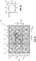
- a ring 52 of masking material 53has been formed circumferentially about projecting portions 50 of individual pillars 47 . Rings 52 form individual mask openings 54 defined by four immediately-surrounding rings 52 in immediately-adjacent rows 16 . Mask openings 54 are between immediately-diagonally-adjacent openings 40 in immediately adjacent rows 16 .
- Material 53 of rings 52may be entirely sacrificial and, accordingly, may comprise any conductive, insulative, and/or semiconductive material(s). Rings 52 may be formed, by way of ideal example, by deposition of material 53 , followed by maskless anisotropic spacer-like etching thereof. In one embodiment and as perhaps best shown in the enlarged view of FIG.
- At least an elevationally outer portion of individual mask openings 54are of a four-sided diamond shape in horizontal cross-section.
- the example depicted four-sided diamond shape of mask openings 54may be considered as comprising four sides 58 .
- the four-sides 58are individually concave, and in one such embodiment as shown are circularly concave.
- Lateral deposition thickness of material 53may be sub-lithographic (i.e., where lithography is used) and/or less than 1 ⁇ 2F (“F” being defined below).
- openings 54may have respective maximum horizontal dimensions that are sub-1 ⁇ 2F and/or sub-lithographic
- rings 52 and pillars 47have been used as a mask while etching material 30 through mask openings 54 to form individual via openings 60 to individual first nodes 26 of individual second transistors 20 .
- Suchmay be conducted using any suitable anisotropic etching chemistry or chemistries and techniques, whether existing or yet-to-be-developed. If individual mask openings 54 are of a four-sided diamond shape in horizontal cross-section, that shape may transfer wholly, partially, or not at all to the bottom of via openings 60 .
- conductive material 62has been formed in individual via openings 60 to electrically couple (in one embodiment, directly electrically couple) to first nodes 26 of second transistors 20 .
- Conductive material 62may be of the same or different composition as that of capacitor nodes 42 and/or 46 .
- conductive material 62is deposited to overfill via openings 60 and be elevationally outward of rings 52 and pillars 47 .
- projecting portions 50 (not shown) of capacitor pillars 47 and rings 52have been removed from being above material 30 (and material 33 ), thus forming pillars 67 of conductive material 62 and forming capacitors 71 comprising capacitor insulator 44 and capacitor nodes 42 and 46 .
- Suchmay occur by any existing or yet-to-be-developed technique, for example by etching, resist etch-back, or chemical mechanical polishing.
- such removalhas been sufficient to remove material 36 (not shown) completely from the substrate, for example back at least to top 27 of dielectric material 33 .
- conductive pillars 67have an elevationally outer portion that is of four-sided diamond shape in horizontal cross-section. In such embodiment, conductive pillars 67 may have their entire elevational thicknesses in respective horizontal cross-sections of a four-sided diamond shape, or may have elevationally inner portions thereof not of such shape.
- conductive material 64has been deposited and patterned to electrically couple (in one embodiment directly electrically couple) to conductive material 62 in individual via openings 60 with one of four immediately-surrounding capacitor pillars 47 , thus forming individual 2T-1C memory cells MC (only one outline MC being shown in FIGS. 23 and 24 for clarity) of an array 75 of such memory cells.
- immediately-adjacent pairs of sense lines 13 , 14may be BL-T and BL-C in the FIG. 1 schematic.
- Conductive material 64 as shownmay be formed by subtractive patterning and etch with or without pitch multiplication, damascene processing with or without pitch multiplication, etc. Regardless and in one embodiment, the above example processing shows conducting the forming of conductive material 62 in via openings 60 and the electrically coupling of those via openings to one of the four immediately-surrounding capacitor pillars 47 in two separate time-spaced conductive material-deposition steps. Conductive material 64 may be of the same or different composition as that of conductive material 62 and the conductive materials of capacitor nodes 42 and/or 46 .
- Conductive materials 62 and 64effectively constitute a part of second capacitor node 46 (and accordingly capacitor 71 ) the result of such materials being directly electrically coupled relative one another (e.g., conductive material 64 being directly against conductive material of capacitor nodes 46 within openings 40 , and conductive material 62 being directly against conductive material 64 ). Accordingly, and in one embodiment, second capacitor node 46 / 64 / 62 is directly against a top 59 of capacitor insulator 44 . Regardless, and in one embodiment, second capacitor node 46 / 64 / 62 is directly above first node 26 of second transistor 20 , and in one embodiment is also directly above first node 26 of first transistor 18 .
- first capacitor node 42is directly electrically coupled to first node 26 of first transistor 18 and second capacitor node 46 / 64 / 62 is directly electrically coupled to first node 26 of second transistor 20 .
- pillar 67 and second transistor 20are longitudinally coaxial.
- Embodiments of the inventionencompass methods independent of forming an array of 2T-1C memory cells, independent of forming memory cells, and independent of forming capacitors.
- an embodiment of the inventionencompasses a method of forming a plurality of rows (e.g., 16 ) of pillar openings (e.g., 40 ) that are inter-row aligned (e.g., as shown FIG. 8 , and regardless of whether those openings will contain a capacitor or other component of a memory cell or of integrated circuitry).
- a pillaris formed in individual of the pillar openings (e.g., 47 , and independent of whether such comprises a material of a capacitor or other operative circuit component that remains as part of the finished circuitry construction).
- the pillarsare formed to project elevationally outward relative to an upper surface of material in which the pillar openings were formed (e.g., as shown in FIG. 14 , and independent of technique by which the pillars are formed to be so-projecting).
- a ring of masking materiale.g., 52 of material 53
- the ringsform individual mask openings (e.g., 54 ) defined by four immediately-surrounding of the rings that are in immediately-adjacent of the rows, with the rings being between immediately-diagonally-adjacent of the pillar openings.
- the rings and pillarsare used as a mask while etching the material in which the pillar openings were formed through the mask openings (e.g., as shown in FIGS. 18 and 19 ) to form individual via openings (e.g., 60 ) that are between the immediately-diagonally-adjacent pillar openings.
- Conductive materiale.g., 62
- the operative circuit componentcomprises a capacitor
- the pillaris formed to comprise conductive material (e.g., material of capacitor node 46 ) and capacitor insulator (e.g., 44 ) of the capacitor and that remains as part of the finished circuitry construction. Portions of the pillars that project elevationally outward comprise the conductive material and the capacitor insulator.
- the capacitorcomprises two nodes (i.e., conductive) separated by the capacitor insulator and the conductive material of only one of the nodes projects elevationally outward relative to the upper surface of the material in which the pillar openings were formed (e.g., materials 46 and 44 as shown in FIG. 14 projecting relative to surface 49 ).
- FIG. 25is a redacted and enhanced version of FIG. 23 to more clearly show “F”
- FIG. 26is a redacted version of FIG. 25 to show area occupied by a single memory cell MC.
- Maximum digit line width and minimum space there-betweenare equal in construction 12 (i.e., each equals F).
- Combined diameter of channel 28 and gate insulator 23is 0.75F.
- Intra-row and inter-row spacing between immediately-adjacent capacitor openings 40are equal to one another, and is 0.25F.
- Maximum access line widthis 3.25F and minimum space between immediately-adjacent access lines 22 is 0.075F.
- memory cell y-direction pitch and x-direction pitcheach equal 4F, thereby with individual memory cells MC occupying a maximum area of 16F 2 (i.e., area occupied by a single unit cell of the memory array).
- Alternate configurations and/or alternate of any one or more of these dimensionsmay be used. By way of examples only, four alternate configurations are described below with respect to FIGS. 27 / 28 , 29 / 30 , 31 / 32 , and 33 / 34 .
- FIGS. 27 and 28show an alternate example construction 12 a .
- Construction 12 a as compared to construction 12has an example y-direction stretch of 1F to a total of 5F, while keeping x-dimensions the same, resulting in individual memory cells MCa being 4F by 5F and individual memory cells thereby occupying a maximum area of 20F 2 .
- FIG. 27shows such y-direction stretch being 0.5F with respect to minimum space between immediately-adjacent access lines 22 a , specifically from 0.75F in construction 12 to 1.25F in construction 12 a .
- FIG. 27also additional shows y-direction stretch being 0.5F with respect to maximum width of access lines 22 a , specifically from 3.25F in construction 12 to 3.75F in construction 12 a .
- capacitors openings 40 a and accordingly resultant capacitorsare arrayed in a 2D rectangular Bravais lattice (as may be more readily perceived by rotating the sheet upon which FIG. 27 lies 90°). Any other attribute(s) or aspect(s) as described herein and/or shown may be used.
- FIGS. 29 and 30show an alternate example construction 12 b .
- Construction 12 bhas 1.75F minimum spacing between immediately-adjacent access lines 22 b and has access line maximum width of 4.25F, resulting in a 4F by 6F individual memory cell MCb occupying a maximum area of 24F 2 . Any other attribute(s) or aspect(s) as described herein and/or shown may be used.
- FIGS. 31 and 32show an alternate example construction 12 c .
- Intra-row spacing between immediately-adjacent capacitor openings 40 cis 0.5F.
- Inter-row spacing between immediately-adjacent capacitor openings 40 cis 0.25F.
- Construction 12 chas 0.46F minimum spacing between immediately-adjacent access lines 22 c and access line maximum width of 2.96F (“F” being equal to digit line maximum width).
- Minimum space between immediately-adjacent digit linesis 1.25F, thereby resulting in a 4.5F by 3.42F individual memory cell MCc occupying a maximum area 15.39F 2 . Any other attribute(s) or aspect(s) as described herein and/or shown may be used.
- FIGS. 33 and 34show an alternate example construction 12 d .
- Intra-row spacing between immediately-adjacent capacitor openings 40 dis 0.5F.
- Inter-row spacing between immediately-adjacent capacitor openings 40 dis 0.25F.
- Construction 12 dhas 0.06F minimum spacing between immediately-adjacent access lines 22 d and access line maximum width of 2.55F (“F” being equal to digit line maximum width).
- Minimum space between immediately-adjacent digit linesis 1.5F, thereby resulting in a 5F by 2.61F individual memory cell MCd occupying a maximum area of 13.05F 2 . Any other attribute(s) or aspect(s) as described herein and/or shown may be used.
- a memory celle.g., MC
- first and second transistorse.g., 18 , 20 , respectively
- a longitudinally-elongated access line 22that is common to the first and second transistors.
- a capacitor(e.g., 71 ) is above the first and second transistors and comprises a conductive first capacitor node (e.g., 42 ) electrically coupled (in one embodiment directly electrically coupled) to a first node (e.g., 26 ) of the first transistor.
- a conductive second capacitor node(e.g., 46 / 64 / 62 ) is electrically coupled (in one embodiment directly electrically coupled) to a first node (e.g., 26 ) of the second transistor.
- a capacitor insulator(e.g., 44 ) is between the first and second capacitor nodes.
- the second capacitor nodecomprises a first elevationally-extending conductive pillar (e.g., 46 ) above the first node of the first transistor.
- a second elevationally-extending conductive pillar(e.g., 67 ) is above the first node of the second transistor.
- Conductive material(e.g., 64 ) is atop, extends between, and directly electrically couples together the first and second pillars.
- the conductive materialis longitudinally-elongated (e.g., along a line 72 in FIG. 25 ) at an angle (i.e., any angle other than the straight angle herein and e.g., angle 73 in FIG. 25 which is shown as 45°) relative to longitudinal orientation (e.g., along a row line 19 ) of the longitudinally-elongated access line within the memory cell.
- the angleis at least 25° relative to the longitudinal orientation of the longitudinally-elongated access line within the memory cell. In one embodiment, such angle is 25° to 60°, in one such embodiment is more than 45°, in one such embodiment is less than 45°, and in one such embodiment is 45°.
- Corresponding lines 72 a , 72 b , 72 c , and 72 dare shown in FIGS. 27, 29, 31, and 33 , respectively.
- Corresponding angles 73 a , 73 b , 73 c , and 73 dare shown in FIGS. 27, 29, 31, and 33 , respectively, and are 51°, 56°, 37°, and 28°, respectively.
- the first and second transistorsare each elevationally-extending, and in one embodiment are in a common horizontal plane relative one another.
- the second capacitor nodeis directly against a top of the capacitor insulator, and in one embodiment is directly above the first node of the second transistor, and in one embodiment is directly above the first node of the first transistor.
- the first capacitor nodeis directly above the first node of the first transistor.
- the first capacitor nodeis directly electrically coupled to the first node of the first transistor and the second capacitor node is directly electrically coupled to the first node of the second transistor.
- the first capacitor node and the first transistorare longitudinally coaxial.
- the second pillarhas an elevationally outer portion that is of four-sided diamond shape in horizontal cross-section.
- a memory cell(e.g., MC) comprises first and second transistors (e.g., 18 , 20 , respectively) laterally displaced relative one another.
- a capacitor(e.g., 71 ) is above the first and second transistors and comprises a conductive first capacitor node (e.g., 42 ) electrically coupled (in one embodiment directly electrically coupled) to a first node (e.g., 26 ) of the first transistor.
- a conductive second capacitor node(e.g., 46 / 64 / 62 ) is electrically coupled (in one embodiment directly electrically coupled) to a first node 26 of the second transistor.
- a capacitor insulator(e.g., 44 ) is between the first and second capacitor nodes.
- the second capacitor nodecomprises a first elevationally-extending conductive pillar (e.g., 46 ) above the first node of the first transistor.
- a second elevationally-extending conductive pillar(e.g., 67 ) is above the first node (e.g., 26 ) of the second transistor.
- Conductive materiale.g., 64
- a first digit line(e.g., 13 ) is electrically coupled to a second node (e.g., 24 ) of the first transistor and a second digit line (e.g., 14 ) is electrically coupled to a second node (e.g., 24 ) of the second transistor.
- the first and second digit linesare longitudinally-elongated.
- Such conductive material of the second capacitor nodeis longitudinally-elongated (e.g., along line 72 in FIG. 25 ) at an angle (e.g., angle 77 in FIG. 25 which is shown as 45°) other than 90° relative to longitudinal orientation (e.g., along column lines 15 ) of each of the first and second longitudinally-elongated digit lines.
- angleis 30° to 65°, in one such embodiment is more than 45°, in one such embodiment is less than 45°, and in one such embodiment is 45°.
- Corresponding angles 77 a , 77 b , 77 c , and 77 dare shown in FIGS.
- the first capacitor nodecomprises a container shape.
- the second transistoris a vertical transistor, and the second pillar and the second transistor are longitudinally coaxial.
- a memory cell(e.g., MC) comprises first and second transistors (e.g., 18 , 20 , respectively) laterally displaced relative one another and an access line (e.g., 22 ) that is common to the first and second transistors.
- a capacitor(e.g., 71 ) is above the first and second transistors.
- the capacitorcomprises a conductive first capacitor node (e.g., 42 ) electrically coupled (in one embodiment directly electrically coupled) to a first node (e.g., 26 ) of the first transistor.
- a conductive second capacitor node(e.g., 46 / 64 / 62 ) is electrically coupled to a first node (e.g., 26 ) of the second transistor.
- a capacitor insulator(e.g., 44 ) is between the first and second capacitor nodes.
- a second node (e.g., 24 ) of the first transistoris electrically coupled (in one embodiment directly electrically coupled) to a first digit line (e.g., 13 ) at a first longitudinal location (e.g., 97 in FIGS. 25, 27, 29, 31, and 33 ) along the first digit line.
- a second node (e.g., 24 ) of the second transistoris electrically coupled (in one embodiment directly electrically coupled) to a second digit line (e.g., 14 ) at a second longitudinal location (e.g., 99 in FIGS. 25, 27, 29, 31, and 33 ) along the second digit line.
- the first and second digit linesare parallel relative one another within the memory cell.
- a horizontal line (e.g., 72 ) through centers of the first and second longitudinal locationsis angled at least 30 (e.g., angle 77 , 77 a , 77 b , 77 c , or 77 d ) relative to longitudinal orientation (e.g., along column lines 15 ) of the first and second digit lines within the memory cell.
- such angleis 30° to 65°, in one such embodiment is more than 45°, in one such embodiment is less than 45°, and in one such embodiment is 45°.
- the access linehas a maximum width that is greater than that of the first and second digit lines.
- the first and second digit linestogether have a minimum pitch within the memory cell, and the memory cell, occupies a maximum horizontal area of no more than 24F 2 , where “F” is one of a) one-half of the minimum digit line pitch, or b) digit line maximum width.
- the maximum areais no more than 20 F 2 , in one embodiment is no more than 16F 2 , and in one embodiment is no more than 14F 2 .
- a two transistor-one capacitor memory cell(e.g., MC) comprises first and second transistors (e.g., 18 , 20 , respectively) laterally displaced relative one another.
- a capacitore.g., 71
- a capacitoris above the first and second transistors and comprises a conductive first capacitor node (e.g., 42 ) directly above and electrically coupled to a first node (e.g., 26 ) of the first transistor.
- a conductive second capacitor node(e.g., 46 / 64 / 62 ) is directly above the first and second transistors and electrically couples to a first node (e.g., 26 ) of the second transistor.
- a capacitor insulator(e.g., 44 ) is between the first and second capacitor nodes.
- the second capacitor nodecomprises an elevationally-extending conductive pillar (e.g., 46 ) directly above the first node of the second transistor.
- a conductive pillarhas an elevationally outer portion that is of a four-sided diamond shape in horizontal cross-section. In one embodiment, the four sides of the four-sided diamond shape are individually concave, and in one such embodiment are circularly concave. Any other attribute(s) or aspect(s) as described herein and/or shown may be used.
- an array (e.g., 75 ) of two transistor-one capacitor memory cellscomprises columns (e.g., 15 ) of digit lines (e.g., 13 , 14 ) and rows (e.g., 19 ) of access lines (e.g., 22 ).
- the digit linescomprise first alternating digit lines (e.g., 13 ) and second alternating digit lines (e.g., 14 ).
- the second alternating digit linesindividually are between immediately adjacent of the first alternating digit lines.
- Individual of the rows of access linesare operatively adjacent the channels of the first and second transistors.
- Individual capacitorse.g., 71
- the capacitorsindividually comprise a first capacitor node (e.g., 42 ) electrically coupled to the first transistor of the individual pair.
- a second capacitor nodee.g., 46 / 64 / 62
- a capacitor insulatore.g., 44
- the capacitorsare arrayed in a 2D square Bravais lattice, and in one embodiment are arrayed in a 2D rectangular Bravais lattice. Any other attribute(s) or aspect(s) as described herein and/or shown may be used.
- an array (e.g., 75 ) of two transistor-one capacitor (2T-1C) memory cellscomprises rows (e.g., 19 ) of access lines (e.g., 22 ) and columns (e.g., 15 ) of digit lines (e.g., 13 , 14 ).
- Individual of the columnscomprise either a) one digit line (e.g., 13 ) individually electrically coupling to one source/drain region (e.g., 26 ) of one of an individual first transistor (e.g., 18 ) of individual 2T-1C memory cells within the array and interconnecting the first transistors in that column, or b) another digit line (e.g., 14 ) individually electrically coupling to one source/drain region (e.g., 26 ) of an individual second transistor (e.g., 20 ) of the individual 2T-1C memory cell and interconnecting the second transistors in that column.
- Individual of the rowscomprise an access line (e.g., 22 ) above the digit lines.
- the access lineextends operatively adjacent transistor channels (e.g., 28 ) of the first and second transistors and inter-connects the first and second transistors in that row.
- the individual 2T-1C memory cellscomprise a capacitor (e.g., 71 ) above the first transistor and above the second transistor of the individual 2T-1C memory cell.
- the capacitorcomprises a conductive first capacitor node (e.g., 42 ) electrically coupled (in one embodiment directly electrically coupled) to the first transistor of the individual 2T-1C memory cell.
- a conductive second transistor node(e.g., 46 / 64 / 62 ) is electrically coupled to the second transistor of the individual 2T-1C memory cell.
- a capacitor insulator(e.g., 44 ) is between the first and second capacitor nodes.
- the second capacitor nodecomprises a first elevationally-extending conductive pillar (e.g., 47 ) above the first node of the first transistor.
- a second elevationally-extending conductive pillare.g., 67 ) is above the first node of the second transistor.
- Conductive material(e.g., 64 ) is atop, extends between, and directly electrically couples together the first and second pillars.
- Such conductive materialis at least one of a) longitudinally-elongated (e.g., along a line 72 , 72 a , 72 b , 72 c , or 72 d ) at an angle (e.g., 77 , 77 a , 77 b , 77 c , or 77 d ) other than 90° relative to the columns of the digit lines, or b) longitudinally-elongated (e.g., along a row line 19 ) at an angle (e.g., 73 , 73 a , 73 b , 73 c , or 73 d ) relative to the rows of access lines. Any other attribute(s) or aspect(s) as described herein and/or shown may be used.
- an array (e.g., 75 ) of two transistor-one capacitor (2T-1C) memory cellscomprises rows (e.g., 19 ) of access line (e.g., 22 ) and columns (e.g., 15 ) of digit lines (e.g., 13 , 14 ).
- Individual of the columnscomprise either a) one digit line (e.g., 13 ) individually electrically coupling to one source/drain region (e.g., 26 ) of one of an individual first transistor (e.g., 18 ) of individual 2T-1C memory cells within the array and interconnecting the first transistors in that column, or b) another digit line (e.g., 14 ) individually electrically coupling to one source/drain region (e.g., 26 ) of an individual second transistor (e.g., 20 ) of the individual 2T-1C memory cell and interconnecting the second transistors in that column.
- Individual of the rowscomprise an access line (e.g., 22 ) above the digit lines.
- the access lineextends operatively adjacent transistor channels (e.g., 28 ) of the first and second transistors and inter-connects the first and second transistors in that row.
- the access linehas a maximum width that is greater than that of each of the one and other digit lines.
- the individual 2T-1C memory cellscomprise a capacitor (e.g., 71 ) above the first transistor and above the second transistor of the individual 2T-1C memory cell.
- the maximum widthis at least two times greater than that of each of the one and other digit lines, in one embodiment is at least three times greater, and in one embodiment is no more than five times greater than that of the one and other digit lines.
- Wider access linesmay exhibit reduced resistance longitudinally along such lines. Any other attribute(s) or aspect(s) as described herein and/or shown may be used.
- Constructions 12 , 12 a , 12 b , 12 c , and 12 cshow transistors 18 , 20 as comprising field effect transistors and which extend elevationally. However, any suitable alternate transistors may be used, for example bipolar junction transistors and regardless of whether such extend elevationally.
- the same sign voltagei.e., positive or negative
- the same sign voltageis applied to the respective one and other sides of the capacitor electrodes when reading and writing to each memory cell within the array. This is at least because constructions and/or materials of the conductive electrodes of the capacitors may be different relative to one another. If different capacitors in different rows had their capacitor electrodes subjected to opposite sign polarities, different capacitors may have different current vs. voltage profiles for different transistors within the array and which may be highly undesirable.
- capacitor electrode 42 and capacitor electrode 46 / 64 / 62 of an individual memory cell MCare shown as inherently being of different construction relative to one another regardless of whether both are formed of the same material(s) as the other. It is desirable in 2T-1C memory cell operation, whether read or write, that each capacitor node 42 in the array always have one sign voltage (i.e., positive or negative) and that each capacitor node 46 / 64 / 62 always have the opposite sign voltage (i.e., the other of positive and negative). In other words, it is typically desirable that all memory cells within an array have matched access polarities.
- Constructions as provided hereinfor example channel-offset first and second transistors and/or that diagonally connect with respect to one of the capacitor plates between the transistors, may be used to enable all like capacitor electrodes within the array to have the same sign voltage potential for all read and write operations.
- a memory cellcomprises first and second transistors laterally displaced relative one another and comprising a longitudinally-elongated access line that is common to the first and second transistors.
- a capacitoris above the first and second transistors and comprises a conductive first capacitor node electrically coupled to a first node of the first transistor.
- a conductive second capacitor nodeis electrically coupled to a first node of the second transistor.
- a capacitor insulatoris between the first and second capacitor nodes.
- the second capacitor nodecomprises a first elevationally-extending conductive pillar above the first node of the first transistor.
- a second elevationally-extending conductive pillaris above the first node of the second transistor.
- Conductive materialis atop, extends between, and directly electrically couples together the first and second pillars.
- the conductive materialis longitudinally elongated at an angle relative to longitudinal orientation of the longitudinally-elongated access line within the memory cell.
- a memory cellcomprises first and second transistors laterally displaced relative one another.
- a capacitoris above the first and second transistors and comprises a conductive first capacitor node electrically coupled to a first node of the first transistor.
- a conductive second capacitor nodeis electrically coupled to a first node of the second transistor.
- a capacitor insulatoris between the first and second capacitor nodes.
- the second capacitor nodecomprises a first elevationally-extending conductive pillar above the first node of the first transistor.
- a second elevationally-extending conductive pillaris above the first node of the second transistor.
- Conductive materialis atop, extends between, and directly electrically couples together the first and second pillars.
- a first digit lineis electrically coupled to a second node of the first transistor and a second digit line is electrically coupled to a second node of the second transistor.
- the first and second digit linesare longitudinally elongated.
- the conductive material of the second capacitor nodeis longitudinally elongated at an angle other than 90° relative to longitudinal orientation of each of the first and second longitudinally-elongated digit lines.
- a memory cellcomprises first and second transistors laterally displaced relative one another and comprises an access line that is common to the first and second transistors.
- a capacitoris above the first and second transistors.
- the capacitorcomprises a conductive first capacitor node electrically coupled to a first node of the first transistor.
- a conductive second capacitor nodeis electrically coupled to a first node of the second transistor.
- a capacitor insulatoris between the first and second capacitor nodes.
- a second node of the first transistoris electrically coupled to a first digit line at a first longitudinal location along the first digit line and a second node of the second transistor is electrically coupled to a second digit line at a second longitudinal location along the second digit line.
- the first and second digit linesare parallel relative one another within the memory cell.
- a horizontal line through centers of the first and second longitudinal locationsis angled at least 30° relative to longitudinal orientation of the first and second digit lines within the memory cell.
- a two transistor-one capacitor memory cellcomprises first and second transistors laterally displaced relative one another.
- a capacitoris above the first and second transistors.
- the capacitorcomprises a conductive first capacitor node directly above and electrically coupled to a first node of the first transistor.
- a conductive second capacitor nodeis directly above the first and second transistors and is electrically coupled to a first node of the second transistor.
- a capacitor insulatoris between the first and second capacitor nodes.
- the second capacitor nodecomprises an elevationally-extending conductive pillar directly above the first node of the second transistor.
- the conductive pillarhas an elevationally outer portion that is of four-sided diamond shape in horizontal cross-section.
- an array of two transistor-one capacitor memory cellscomprise columns of digit lines and rows of access lines.
- the digit linescomprise first alternating digit lines and second alternating digit lines.
- the second alternating digit linesindividually are between immediately adjacent of the first alternating digit lines.
- Rows of elevationally-extending first field effect transistorsindividually have an elevationally inner of their source/drain regions electrically coupled to one of the individual first alternating digit lines.
- Rows of elevationally-extending second first field effect transistorsindividually have an elevationally inner of their source/drain regions electrically coupled to one of the individual second alternating digit lines.
- Channels of the first and second transistorsare inter-row staggered. Individual of the rows of access lines are operatively adjacent the channels of the first and second transistors.
- the capacitorsindividually comprise a conductive first capacitor node electrically coupled to the first transistor of the individual pair.
- a conductive second capacitor nodeis electrically coupled to the second transistor of the individual pair.
- a capacitor insulatoris between the first and second capacitor nodes.
- an array of two transistor-one capacitor (2T-1C) memory cellswhere the array comprises rows of access lines and columns of digit lines, has individual of the columns comprising either a) one digit line individually electrically coupling to one source/drain region of one of an individual first transistor of individual 2T-1C memory cells within the array and interconnecting the first transistors in that column, or b) another digit line individually electrically coupling to one source/drain region of an individual second transistor of the individual 2T-1C memory cell and interconnecting the second transistors in that column.
- Individual of the rowscomprise an access line above the digit lines. The access line extends operatively adjacent transistor channels of the first and second transistors and interconnects the first and second transistors along that row.
- the individual 2T-1C memory cellscomprise a capacitor above the first transistor and above the second transistor of the individual 2T-1C memory cell.
- the capacitorcomprises a conductive first capacitor node electrically coupled to the first transistor of the individual 2T-1C memory cell.
- a conductive second capacitor nodeis electrically coupled to the second transistor of the individual 2T-1C memory cell.
- a capacitor insulatoris between the first and second capacitor nodes.
- the second capacitor nodecomprises a first elevationally-extending conductive pillar above the first node of the first transistor.
- a second elevationally-extending conductive pillaris above the first node of the second transistor.
- Conductive materialis atop, extends between, and directly electrically couples together the first and second pillars; the conductive material is at least one of a) longitudinally elongated at an angle other than 90° relative to the columns of the digit lines, or b) longitudinally elongated at an angle relative to the rows of access lines.
- an array of two transistor-one capacitor (2T-1C) memory cellswhere the array comprises rows of access lines and columns of digit lines, has individual of the columns comprising either a) one digit line individually electrically coupling to one source/drain region of one of an individual first transistor of individual 2T-1C memory cells within the array and interconnecting the first transistors in that column, or b) another digit line individually electrically coupling to one source/drain region of an individual second transistor of the individual 2T-1C memory cell and interconnecting the second transistors in that column.
- Individual of the rowscomprise an access line above the digit lines.
- the access lineextends operatively adjacent transistor channels of the first and second transistors and interconnects the first and second transistors along that row and has a maximum width that is greater than that of each of the one and other digit lines.
- the individual 2T-1C memory cellscomprise a capacitor above the first transistor and above the second transistor of the individual 2T-1C memory cell.
- a method used in fabricating integrated circuitrycomprises forming a plurality of rows of pillar openings that are inter-row aligned.
- a pillaris formed in individual of the pillar openings.
- the pillarsproject elevationally outward relative to an upper surface of material in which the pillar openings were formed.
- a ring of masking materialis circumferentially about the individual pillars.
- the ringsform individual mask openings defined by four immediately-surrounding of the rings that are in immediately-adjacent of the rows and that are between immediately-diagonally-adjacent of the pillar openings in the immediately-adjacent rows.
- the rings and pillarsare used as a mask while etching the material in which the pillar openings were formed through the mask openings to form individual via openings that are between the immediately-diagonally-adjacent pillar openings in the immediately-adjacent rows.
- Conductive material in the individual via openingsis directly electrically coupled to an operative circuit component formed in one of four of the pillar openings that immediately surround the individual via openings.
- a method of forming an array of two transistor-one capacitor memory cellscomprises forming columns of digit lines. Rows of elevationally-extending first and second field effect transistors are formed to individually have an elevationally inner of their source/drain regions electrically coupled to individual of the digit lines.
- the first and second transistorscomprise access lines above the digit lines, and individual of the first and second transistors comprise a gate comprising part of individual of the access lines.
- a plurality of capacitor openingsare formed to individually extend to an elevationally outer source/drain region of the individual first transistors.
- a capacitor pillaris formed in individual of the capacitor openings.
- the capacitor pillaris formed to comprise a conductive first capacitor node electrically coupled to individual of the elevationally outer source/drain regions of the individual first transistors, a conductive second capacitor node, and a capacitor insulator between the first and second capacitor nodes.
- Material in which the capacitor openings were formedis recessed to result in uppermost portions of the capacitor pillars projecting elevationally outward relative to an upper surface of the material in which the capacitor openings were formed.
- a ring of masking materialis formed circumferentially about the projecting portions of individual of the capacitor pillars.
- the ringsform individual mask openings defined by four immediately-surrounding of the rings in immediately-adjacent of the rows and that are between immediately-diagonally-adjacent of the capacitor openings in the immediately-adjacent rows.
- the rings and capacitor pillarsare used as a mask while etching the material in which the capacitor openings were formed through the mask openings to form individual via openings to individual of elevationally outer source/drain regions of the individual second transistors.
- the projecting portions of the capacitor pillarsare removed as are the rings from being above the material in which the capacitor openings were formed.
- Conductive materialis formed in the individual via openings electrically coupled to the individual elevationally outer source/drain region of the individual second transistors and electrically coupled to one of four immediately-surrounding of the capacitor pillars.
Landscapes
- Engineering & Computer Science (AREA)
- Manufacturing & Machinery (AREA)
- Semiconductor Memories (AREA)
Abstract
Description
Claims (20)
Priority Applications (2)
| Application Number | Priority Date | Filing Date | Title |
|---|---|---|---|
| US15/852,870US11211384B2 (en) | 2017-01-12 | 2017-12-22 | Memory cells, arrays of two transistor-one capacitor memory cells, methods of forming an array of two transistor-one capacitor memory cells, and methods used in fabricating integrated circuitry |
| US17/528,128US11968821B2 (en) | 2017-01-12 | 2021-11-16 | Methods used in fabricating integrated circuitry and methods of forming 2T-1C memory cell arrays |
Applications Claiming Priority (2)
| Application Number | Priority Date | Filing Date | Title |
|---|---|---|---|
| US201762445574P | 2017-01-12 | 2017-01-12 | |
| US15/852,870US11211384B2 (en) | 2017-01-12 | 2017-12-22 | Memory cells, arrays of two transistor-one capacitor memory cells, methods of forming an array of two transistor-one capacitor memory cells, and methods used in fabricating integrated circuitry |
Related Child Applications (1)
| Application Number | Title | Priority Date | Filing Date |
|---|---|---|---|
| US17/528,128DivisionUS11968821B2 (en) | 2017-01-12 | 2021-11-16 | Methods used in fabricating integrated circuitry and methods of forming 2T-1C memory cell arrays |
Publications (2)
| Publication Number | Publication Date |
|---|---|
| US20180197864A1 US20180197864A1 (en) | 2018-07-12 |
| US11211384B2true US11211384B2 (en) | 2021-12-28 |
Family
ID=62783456
Family Applications (2)
| Application Number | Title | Priority Date | Filing Date |
|---|---|---|---|
| US15/852,870ActiveUS11211384B2 (en) | 2017-01-12 | 2017-12-22 | Memory cells, arrays of two transistor-one capacitor memory cells, methods of forming an array of two transistor-one capacitor memory cells, and methods used in fabricating integrated circuitry |
| US17/528,128Active2038-05-14US11968821B2 (en) | 2017-01-12 | 2021-11-16 | Methods used in fabricating integrated circuitry and methods of forming 2T-1C memory cell arrays |
Family Applications After (1)
| Application Number | Title | Priority Date | Filing Date |
|---|---|---|---|
| US17/528,128Active2038-05-14US11968821B2 (en) | 2017-01-12 | 2021-11-16 | Methods used in fabricating integrated circuitry and methods of forming 2T-1C memory cell arrays |
Country Status (4)
| Country | Link |
|---|---|
| US (2) | US11211384B2 (en) |
| CN (1) | CN110192280A (en) |
| TW (1) | TWI671860B (en) |
| WO (1) | WO2018132250A1 (en) |
Cited By (2)
| Publication number | Priority date | Publication date | Assignee | Title |
|---|---|---|---|---|
| US20220351768A1 (en)* | 2017-05-09 | 2022-11-03 | Micron Technology, Inc. | Ferroelectric devices and ferroelectric memory cells |
| US20230255014A1 (en)* | 2022-02-10 | 2023-08-10 | Tokyo Electron Limited | Technologies for fabricating a vertical dram structure |
Families Citing this family (32)
| Publication number | Priority date | Publication date | Assignee | Title |
|---|---|---|---|---|
| CN109155311A (en) | 2016-08-31 | 2019-01-04 | 美光科技公司 | memory cell and memory array |
| US10056386B2 (en) | 2016-08-31 | 2018-08-21 | Micron Technology, Inc. | Memory cells and memory arrays |
| US10355002B2 (en)* | 2016-08-31 | 2019-07-16 | Micron Technology, Inc. | Memory cells, methods of forming an array of two transistor-one capacitor memory cells, and methods used in fabricating integrated circuitry |
| EP3840046B1 (en) | 2016-08-31 | 2025-03-19 | Micron Technology, Inc. | Memory cells and memory arrays |
| CN109155145B (en) | 2016-08-31 | 2022-11-01 | 美光科技公司 | Memory array |
| US11211384B2 (en) | 2017-01-12 | 2021-12-28 | Micron Technology, Inc. | Memory cells, arrays of two transistor-one capacitor memory cells, methods of forming an array of two transistor-one capacitor memory cells, and methods used in fabricating integrated circuitry |
| US10825815B2 (en) | 2017-05-08 | 2020-11-03 | Micron Technology, Inc. | Memory arrays |
| US11043499B2 (en) | 2017-07-27 | 2021-06-22 | Micron Technology, Inc. | Memory arrays comprising memory cells |
| CN110753962A (en) | 2017-08-29 | 2020-02-04 | 美光科技公司 | memory circuit |
| US10461149B1 (en) | 2018-06-28 | 2019-10-29 | Micron Technology, Inc. | Elevationally-elongated conductive structure of integrated circuitry, method of forming an array of capacitors, method of forming DRAM circuitry, and method of forming an elevationally-elongated conductive structure of integrated circuitry |
| US10475796B1 (en)* | 2018-06-28 | 2019-11-12 | Micron Technology, Inc. | Method of forming an array of capacitors, a method of forming DRAM circuitry, and a method of forming an elevationally-elongated conductive structure of integrated circuitry |
| US10950618B2 (en)* | 2018-11-29 | 2021-03-16 | Micron Technology, Inc. | Memory arrays |
| US10886285B2 (en)* | 2018-12-07 | 2021-01-05 | Micron Technology, Inc. | Memory circuitry and methods of forming memory circuitry |
| US11335686B2 (en)* | 2019-10-31 | 2022-05-17 | Intel Corporation | Transistors with back-side contacts to create three dimensional memory and logic |
| US11257822B2 (en) | 2019-11-21 | 2022-02-22 | Intel Corporation | Three-dimensional nanoribbon-based dynamic random-access memory |
| US11289497B2 (en) | 2019-12-27 | 2022-03-29 | Kepler Computing Inc. | Integration method of ferroelectric memory array |
| US11482528B2 (en) | 2019-12-27 | 2022-10-25 | Kepler Computing Inc. | Pillar capacitor and method of fabricating such |
| JP2021108331A (en) | 2019-12-27 | 2021-07-29 | キオクシア株式会社 | Semiconductor storage device |
| US11430861B2 (en) | 2019-12-27 | 2022-08-30 | Kepler Computing Inc. | Ferroelectric capacitor and method of patterning such |
| US11127744B2 (en)* | 2020-01-08 | 2021-09-21 | Micron Technology, Inc. | Memory devices and methods of forming memory devices |
| US11211385B2 (en)* | 2020-02-25 | 2021-12-28 | Nanya Technology Corporation | Semiconductor device and manufacturing method thereof |
| US12324143B2 (en)* | 2020-04-17 | 2025-06-03 | Micron Technology, Inc. | Methods of utilizing etch-stop material during fabrication of capacitors, integrated assemblies comprising capacitors |
| US11672128B2 (en) | 2020-07-20 | 2023-06-06 | Micron Technology, Inc. | Methods of incorporating leaker devices into capacitor configurations to reduce cell disturb, and capacitor configurations incorporating leaker devices |
| US11961881B2 (en)* | 2020-08-13 | 2024-04-16 | Changxin Memory Technologies, Inc. | Method for forming semiconductor structure and semiconductor structure |
| CN114078776A (en)* | 2020-08-13 | 2022-02-22 | 长鑫存储技术有限公司 | Method for forming semiconductor structure and semiconductor structure |
| US11706927B2 (en)* | 2021-03-02 | 2023-07-18 | Micron Technology, Inc. | Memory devices and methods of forming memory devices |
| US11792998B1 (en) | 2021-06-11 | 2023-10-17 | Kepler Computing Inc. | Process integration flow for embedded memory with multi-pocket masks for decoupling processing of memory areas from non-memory areas |
| US11785762B2 (en)* | 2021-06-30 | 2023-10-10 | Micron Technology, Inc. | Memory circuitry and method used in forming memory circuitry |
| US11695072B2 (en) | 2021-07-09 | 2023-07-04 | Micron Technology, Inc. | Integrated assemblies and methods of forming integrated assemblies |
| US12035536B2 (en) | 2021-07-19 | 2024-07-09 | Micron Technology, Inc. | Integrated assemblies and methods of forming integrated assemblies |
| US11917834B2 (en) | 2021-07-20 | 2024-02-27 | Micron Technology, Inc. | Integrated assemblies and methods of forming integrated assemblies |
| US20230411386A1 (en)* | 2022-06-20 | 2023-12-21 | International Business Machines Corporation | Method and structure of forming contacts and gates for staggered fet |
Citations (113)
| Publication number | Priority date | Publication date | Assignee | Title |
|---|---|---|---|---|
| US4103342A (en) | 1976-06-17 | 1978-07-25 | International Business Machines Corporation | Two-device memory cell with single floating capacitor |
| US4554570A (en) | 1982-06-24 | 1985-11-19 | Rca Corporation | Vertically integrated IGFET device |
| JPH03205867A (en) | 1990-01-08 | 1991-09-09 | Nec Corp | Semiconductor memory |
| US5066607A (en) | 1987-11-30 | 1991-11-19 | Texas Instruments Incorporated | Method of making a trench DRAM cell with dynamic gain |
| US5146300A (en) | 1989-11-27 | 1992-09-08 | Mitsubishi Denki Kabushiki Kaisha | Semiconductor integrated circuit device having improved stacked capacitor and manufacturing method therefor |
| US5299155A (en) | 1991-03-01 | 1994-03-29 | Sharp Kabushiki Kaisha | Dynamic random access memory device with capacitor between vertically aligned FETs |
| US5389810A (en) | 1992-03-27 | 1995-02-14 | Matsushita Electric Industrial Co., Ltd. | Semiconductor device having at least one symmetrical pair of MOSFETs |
| US5398200A (en) | 1992-03-02 | 1995-03-14 | Motorola, Inc. | Vertically formed semiconductor random access memory device |
| EP0706187A2 (en) | 1994-09-22 | 1996-04-10 | Matsushita Electric Industrial Co., Ltd. | Ferroelectric memory |
| JPH08147986A (en) | 1994-11-28 | 1996-06-07 | Internatl Business Mach Corp <Ibm> | Control circuit of associative memory and associative memorydevice |
| JPH08264764A (en) | 1995-03-22 | 1996-10-11 | Toshiba Corp | Semiconductor device |
| US5571743A (en) | 1993-01-19 | 1996-11-05 | International Business Machines Corporation | Method of making buried-sidewall-strap two transistor one capacitor trench cell |
| US5586078A (en) | 1994-09-22 | 1996-12-17 | Kabushiki Kaisha Toshiba | Dynamic type memory |
| US5646900A (en) | 1995-01-12 | 1997-07-08 | Mitsubishi Denki Kabushiki Kaisha | Sense amplifier including MOS transistors having threshold voltages controlled dynamically in a semiconductor memory device |
| US5830791A (en) | 1995-09-06 | 1998-11-03 | Lg Semicon Co., Ltd. | Manufacturing process for a DRAM with a buried region |
| US6028806A (en) | 1998-05-22 | 2000-02-22 | Micron Technology, Inc. | Semiconductor memory with local phase generation from global phase signals and local isolation signals |
| US6141286A (en) | 1998-08-21 | 2000-10-31 | Micron Technology, Inc. | Embedded DRAM architecture with local data drivers and programmable number of data read and data write lines |
| US6154387A (en) | 1998-02-19 | 2000-11-28 | Sharp Kabushiki Kaisha | Semiconductor memory device utilizing a polarization state of a ferroelectric film |
| US20010053088A1 (en) | 1998-04-14 | 2001-12-20 | Micron Technology, Inc. | Circuits and methods for a memory cell with a trench plate trench capacitor and a vertical bipolar read device |
| US20020044477A1 (en) | 2000-10-17 | 2002-04-18 | Yoshiaki Takeuchi | Ferroelectric memory device |
| US20020093865A1 (en) | 2001-01-16 | 2002-07-18 | Matsushita Electric Industrial Co., Ltd. | Semiconductor memory device |
| US20020113260A1 (en) | 2001-02-20 | 2002-08-22 | Haining Yang | Rhodium-rich oxygen barriers |
| US20020125508A1 (en)* | 1999-09-02 | 2002-09-12 | Micron Technology, Inc. | Container capacitor structure and method of formation thereof |
| US20020140106A1 (en) | 2001-03-30 | 2002-10-03 | Wlodek Kurjanowicz | Twisted wordline strapping arrangement |
| US20030087499A1 (en) | 2001-11-07 | 2003-05-08 | Lane Richard H | Process for forming metallized contacts to periphery transistors |
| US6563727B1 (en) | 2002-07-31 | 2003-05-13 | Alan Roth | Method and structure for reducing noise effects in content addressable memories |
| US20030169616A1 (en) | 2002-03-08 | 2003-09-11 | Fujitsu Limited | Ferroelectric memory wherein bit line capacitance can be maximized |
| US20030173593A1 (en) | 2002-03-15 | 2003-09-18 | Shinichi Miyatake | Semiconductor memory device |
| US20030185041A1 (en) | 2002-03-29 | 2003-10-02 | Kazuhiko Takahashi | Semiconductor memory device |
| JP2003303901A (en) | 2002-04-08 | 2003-10-24 | Hitachi Ltd | Semiconductor integrated circuit device and method of manufacturing the same |
| US20030202391A1 (en) | 2002-03-19 | 2003-10-30 | Akitoshi Nishimura | Dummy cell structure for 1T1C FeRAM cell array |
| US20030234413A1 (en) | 2002-04-15 | 2003-12-25 | Stmicroelectronics S.R.I. | FeRAM semiconductor memory |
| US6710465B2 (en) | 2001-06-21 | 2004-03-23 | Samsung Electronics Co., Ltd. | Scalable two transistor memory device |
| US20040062101A1 (en) | 2002-09-30 | 2004-04-01 | Fujitsu Limited | Semiconductor memory device and method for arranging memory cells |
| US6720609B2 (en) | 1999-06-16 | 2004-04-13 | Micron Technology, Inc. | Structure for reducing contact aspect ratios |
| US20040090810A1 (en) | 2002-11-12 | 2004-05-13 | Shinzo Sakuma | Ferroelectric memory |
| US20040099886A1 (en) | 2002-11-26 | 2004-05-27 | Howard Rhodes | CMOS imager pixel designs |
| US6744087B2 (en) | 2002-09-27 | 2004-06-01 | International Business Machines Corporation | Non-volatile memory using ferroelectric gate field-effect transistors |
| US20040151020A1 (en) | 2002-11-27 | 2004-08-05 | Peter Beer | Dynamic memory cell |
| US20040174733A1 (en) | 2003-03-05 | 2004-09-09 | International Business Machines Corporation | Structure and System-on-Chip Integration of a Two-Transistor and Two-Capacitor Memory Cell for Trench Technology |
| US20040232497A1 (en) | 2001-12-14 | 2004-11-25 | Satoru Akiyama | Semiconductor device and method for manufacturing the same |
| US20040252542A1 (en) | 2003-06-16 | 2004-12-16 | Katsuhiko Hoya | Ferroelectric memory device |
| US20050023589A1 (en)* | 2003-07-28 | 2005-02-03 | Yuki Yamada | Semiconductor memory device having a ferroelectric capacitor and method of manufacturing the same |
| WO2005093836A2 (en) | 2004-03-11 | 2005-10-06 | Micron Technology, Inc. | Semiconductor constructions having a buried bit line, and methods of forming same |
| US6961271B2 (en) | 2002-09-09 | 2005-11-01 | Samsung Electronics Co., Ltd. | Memory device in which memory cells having complementary data are arranged |
| US20060028859A1 (en) | 2002-11-12 | 2006-02-09 | Micron Technology, Inc. | 6F2 3-Transistor DRAM gain cell |
| US20060046391A1 (en) | 2004-08-30 | 2006-03-02 | Tang Sanh D | Vertical wrap-around-gate field-effect-transistor for high density, low voltage logic and memory array |
| US20060046424A1 (en) | 2004-08-24 | 2006-03-02 | Chance Randal W | Methods of forming semiconductor constructions |
| US20060138466A1 (en) | 2004-12-23 | 2006-06-29 | Jin Choi | Layout of semiconductor memory device and method of controlling capacitance of dummy cell |
| US20060164876A1 (en) | 2003-09-25 | 2006-07-27 | Infineon Technologies Ag | Multi-transistor memory cells |
| US20060211194A1 (en) | 2004-12-13 | 2006-09-21 | Haller Gordon A | Methods of reducing floating body effect |
| US7164595B1 (en) | 2005-08-25 | 2007-01-16 | Micron Technology, Inc. | Device and method for using dynamic cell plate sensing in a DRAM memory cell |
| US20070034928A1 (en) | 2005-08-10 | 2007-02-15 | Micron Technology, Inc. | Capacitor structure for two-transistor dram memory cell and method of forming same |
| KR20070070021A (en) | 2005-12-28 | 2007-07-03 | 난야 테크놀러지 코포레이션 | Semiconductor device and manufacturing method thereof |
| US20070235790A1 (en)* | 2006-04-05 | 2007-10-11 | Kim Yoon-Hae | Capacitor structure of semiconductor device and method of fabricating the same |
| US20070295995A1 (en) | 2006-06-09 | 2007-12-27 | Samsung Electronics Co., Ltd. | Methods of forming a semiconductor device including buried bit lines |
| US7330388B1 (en) | 2005-09-23 | 2008-02-12 | Cypress Semiconductor Corporation | Sense amplifier circuit and method of operation |
| US20080079049A1 (en)* | 2006-08-25 | 2008-04-03 | Lee Se-Young | Embedded Semiconductor Device Including Planarization Resistance Patterns and Method of Manufacturing the Same |
| US7378702B2 (en) | 2004-06-21 | 2008-05-27 | Sang-Yun Lee | Vertical memory device structures |
| US20080253170A1 (en) | 2006-10-03 | 2008-10-16 | Kabushiki Kaisha Toshiba | Semiconductor device |
| US20090008691A1 (en) | 2007-07-02 | 2009-01-08 | Tzung-Han Lee | Dram structure and method of making the same |
| US20090108881A1 (en) | 2007-10-24 | 2009-04-30 | Agere Systems Inc. | Latch-Based Sense Amplifier |
| US20090168489A1 (en) | 2007-12-31 | 2009-07-02 | Texas Instruments Incorporated | Ferroelectric memory devices with partitioned platelines |
| US7558097B2 (en) | 2006-12-28 | 2009-07-07 | Intel Corporation | Memory having bit line with resistor(s) between memory cells |
| US20090212338A1 (en) | 2008-02-26 | 2009-08-27 | Benson Russell A | Semiconductor Constructions, And Methods Of Forming Semiconductor Constructions |
| US7697318B2 (en) | 2006-12-26 | 2010-04-13 | Kabushiki Kaisha Toshiba | Semiconductor memory device |
| US20100112753A1 (en) | 2003-06-24 | 2010-05-06 | Sang-Yun Lee | Semiconductor memory device |
| US20100165704A1 (en) | 2008-12-30 | 2010-07-01 | Cheng-Hsu Wu | Circuit and Method for a High Speed Memory Cell |
| US20100238697A1 (en) | 2008-02-19 | 2010-09-23 | Micron Technology, Inc. | Systems and devices including local data lines and methods of using, making, and operating the same |
| US20100264484A1 (en) | 2009-04-17 | 2010-10-21 | Fujio Masuoka | Semiconductor device |
| US20100295110A1 (en) | 2009-05-22 | 2010-11-25 | Elpida Memory, Inc. | Device and manufacturing method thereof |
| EP2296176A1 (en) | 2009-09-14 | 2011-03-16 | Unisantis Electronics (Japan) Ltd. | SRAM cell with four SGTs and manufacturing method thereof |
| JP2011142256A (en) | 2010-01-08 | 2011-07-21 | Elpida Memory Inc | Semiconductor device and method of manufacturing the same |
| US8018058B2 (en) | 2004-06-21 | 2011-09-13 | Besang Inc. | Semiconductor memory device |
| US20120153371A1 (en) | 2010-12-15 | 2012-06-21 | Powerchip Technology Corporation | Dynamic random access memory cell and array having vertical channel transistor |
| US8394699B2 (en) | 2006-08-21 | 2013-03-12 | Micron Technology, Inc. | Memory arrays and methods of fabricating memory arrays |
| US20130099305A1 (en) | 2011-10-19 | 2013-04-25 | Sua KIM | Semiconductor devices including a vertical channel transistor and methods of fabricating the same |
| US20130161607A1 (en) | 2011-12-23 | 2013-06-27 | Semiconductor Energy Laboratory Co., Ltd. | Semiconductor device |
| US20130214420A1 (en)* | 2012-02-16 | 2013-08-22 | Elpida Memory, Inc. | Semiconductor device |
| US20130221356A1 (en) | 2012-02-29 | 2013-08-29 | Semiconductor Energy Laboratory Co., Ltd. | Semiconductor device |
| US20130235641A1 (en) | 2012-03-06 | 2013-09-12 | Elpida Memory, Inc. | Semiconductor device |
| US20130235642A1 (en) | 2012-03-06 | 2013-09-12 | Micron Technology, Inc. | Arrays Of Vertically-Oriented Transistors, Memory Arrays Including Vertically-Oriented Transistors, And Memory Cells |
| US20130286734A1 (en) | 2012-04-30 | 2013-10-31 | Chun-Yen Chang | Nand flash memory |
| US20140027839A1 (en) | 2010-06-08 | 2014-01-30 | Samsung Electronics Co., Ltd. | Sram devices and methods of manufacturing the same |
| US20140035018A1 (en) | 2012-07-31 | 2014-02-06 | SK Hynix Inc. | Semiconductor devices including vertical transistors and methods of fabricating the same |
| US20140054718A1 (en) | 2012-08-27 | 2014-02-27 | Micron Technology, Inc. | Arrays of Vertically-Oriented Transistors, And Memory Arrays Including Vertically-Oriented Transistors |
| US20140097481A1 (en)* | 2012-10-10 | 2014-04-10 | Stmicroelectronics (Rousset) Sas | Non-volatile memory with vertical selection transistors |
| US20140220749A1 (en) | 2011-08-02 | 2014-08-07 | Nxp B.V. | A vertical mosfet transistor with a vertical capacitor region |
| US20150041885A1 (en) | 2012-01-26 | 2015-02-12 | Ps4 Luxco S.A.R.L. | Semiconductor memory device |
| US20150078056A1 (en) | 2010-12-02 | 2015-03-19 | Micron Technology, Inc. | Arrays Of Nonvolatile Memory Cells |
| US20150102282A1 (en) | 2013-10-14 | 2015-04-16 | Samsung Electronics Co., Ltd. | Semiconductor memory device having three-dimensional cross point array |
| US20150179655A1 (en) | 2013-12-20 | 2015-06-25 | Samsung Electronics Co., Ltd. | Static random access memory (sram) cells including vertical channel transistors and methods of forming the same |
| US20150318285A1 (en) | 2014-04-30 | 2015-11-05 | Stmicroelectronics, Inc. | Dram interconnect structure having ferroelectric capacitors |
| US9245893B1 (en)* | 2014-11-19 | 2016-01-26 | Micron Technology, Inc. | Semiconductor constructions having grooves dividing active regions |
| US20160079247A1 (en) | 2014-09-16 | 2016-03-17 | Samsung Electronics Co., Ltd. | Semiconductor Device |
| US9343507B2 (en) | 2014-03-12 | 2016-05-17 | Sandisk 3D Llc | Dual channel vertical field effect transistor including an embedded electrode |
| US20160181251A1 (en)* | 2014-12-18 | 2016-06-23 | Samsung Electronics Co., Ltd. | Semiconductor device |
| US9378780B1 (en) | 2015-06-16 | 2016-06-28 | National Tsing Hua University | Sense amplifier |
| US9419003B1 (en) | 2015-05-15 | 2016-08-16 | Taiwan Semiconductor Manufacturing Company, Ltd. | Semiconductor devices and methods of manufacture thereof |
| US20170033111A1 (en)* | 2015-07-29 | 2017-02-02 | Semiconductor Energy Laboratory Co., Ltd. | Semiconductor Device, Circuit Board, and Electronic Device |
| US20170053920A1 (en) | 2015-08-19 | 2017-02-23 | Samsung Electronics Co., Ltd. | Method of fabricating semiconductor device |
| US20170186782A1 (en)* | 2015-12-24 | 2017-06-29 | Innolux Corporation | Pixel circuit of active-matrix light-emitting diode and display panel having the same |
| US9698272B1 (en) | 2016-03-16 | 2017-07-04 | Kabushiki Kaisha Toshiba | Transistor and semiconductor memory device |
| CN107100862A (en) | 2016-02-23 | 2017-08-29 | 宝钢特钢有限公司 | large centrifugal fan |
| US20180061840A1 (en) | 2016-08-31 | 2018-03-01 | Micron Technology, Inc. | Memory Cells, Methods Of Forming An Array Of Two Transistor-One Capacitor Memory Cells, And Methods Used In Fabricating Integrated Circuitry |
| US20180061835A1 (en) | 2016-08-31 | 2018-03-01 | Micron Technology, Inc. | Memory Cells and Memory Arrays |
| US10020311B1 (en) | 2017-08-02 | 2018-07-10 | Ap Memory Technology Corporation | Semiconductor memory device provided with DRAM cell including two transistors and common capacitor |
| US10019025B2 (en)* | 2015-07-30 | 2018-07-10 | Semiconductor Energy Laboratory Co., Ltd. | Semiconductor device and electronic device |
| US20180197864A1 (en) | 2017-01-12 | 2018-07-12 | Micron Technology, Inc. | Memory Cells, Arrays Of Two Transistor-One Capacitor Memory Cells, Methods Of Forming An Array Of Two Transistor-One Capacitor Memory Cells, And Methods Used In Fabricating Integrated Circuitry |
| US10079235B2 (en) | 2016-08-31 | 2018-09-18 | Micron Technology, Inc. | Memory cells and memory arrays |
| US20190019544A1 (en)* | 2017-07-17 | 2019-01-17 | Micron Technology, Inc. | Memory Circuitry |
| US10319724B2 (en) | 2016-08-31 | 2019-06-11 | Micron Technology, Inc. | Memory cells and memory arrays |
| US10381357B2 (en) | 2017-08-31 | 2019-08-13 | Micron Technology, Inc. | Apparatuses having memory cells with two transistors and one capacitor, and having body regions of the transistors coupled with reference voltages |
Family Cites Families (52)
| Publication number | Priority date | Publication date | Assignee | Title |
|---|---|---|---|---|
| JPH088342B2 (en) | 1989-11-27 | 1996-01-29 | 三菱電機株式会社 | Semiconductor integrated circuit device |
| US5256588A (en)* | 1992-03-23 | 1993-10-26 | Motorola, Inc. | Method for forming a transistor and a capacitor for use in a vertically stacked dynamic random access memory cell |
| US5864181A (en) | 1993-09-15 | 1999-01-26 | Micron Technology, Inc. | Bi-level digit line architecture for high density DRAMs |
| KR0139303B1 (en) | 1993-09-16 | 1998-06-01 | 사토 후미오 | A sensing amplifier |
| JP3004177B2 (en) | 1993-09-16 | 2000-01-31 | 株式会社東芝 | Semiconductor integrated circuit device |
| JP3226433B2 (en) | 1994-09-22 | 2001-11-05 | 松下電器産業株式会社 | Ferroelectric memory device |
| JP3270294B2 (en) | 1995-01-05 | 2002-04-02 | 株式会社東芝 | Semiconductor storage device |
| US7052941B2 (en) | 2003-06-24 | 2006-05-30 | Sang-Yun Lee | Method for making a three-dimensional integrated circuit structure |
| JP3235544B2 (en) | 1997-10-29 | 2001-12-04 | 日本電気株式会社 | Semiconductor storage device |
| US6246083B1 (en) | 1998-02-24 | 2001-06-12 | Micron Technology, Inc. | Vertical gain cell and array for a dynamic random access memory |
| JP2000349171A (en) | 1999-06-04 | 2000-12-15 | Sony Corp | Semiconductor memory cell |
| US6496402B1 (en) | 2000-10-17 | 2002-12-17 | Intel Corporation | Noise suppression for open bit line DRAM architectures |
| US6768687B2 (en) | 2000-12-15 | 2004-07-27 | Sony Corporation | Memory array |
| JP3966718B2 (en) | 2001-11-28 | 2007-08-29 | 富士通株式会社 | Semiconductor memory device |
| US6593610B2 (en)* | 2001-12-13 | 2003-07-15 | Micron Technology, Inc. | Memory cell arrays |
| DE10204688C1 (en) | 2002-02-06 | 2003-10-09 | Infineon Technologies Ag | Memory chip with improved electrical properties |
| US7038943B2 (en) | 2002-05-28 | 2006-05-02 | Koninklijke Philips Electronics N.V. | Memory array having 2T memory cells |
| US6794699B2 (en) | 2002-08-29 | 2004-09-21 | Micron Technology Inc | Annular gate and technique for fabricating an annular gate |
| US8445946B2 (en) | 2003-12-11 | 2013-05-21 | International Business Machines Corporation | Gated diode memory cells |
| US7027326B2 (en) | 2004-01-05 | 2006-04-11 | International Business Machines Corporation | 3T1D memory cells using gated diodes and methods of use thereof |
| US6936479B2 (en)* | 2004-01-15 | 2005-08-30 | Hewlett-Packard Development Company, L.P. | Method of making toroidal MRAM cells |
| US7098105B2 (en) | 2004-05-26 | 2006-08-29 | Micron Technology, Inc. | Methods for forming semiconductor structures |
| US7365432B2 (en) | 2004-08-23 | 2008-04-29 | Taiwan Semiconductor Manufacturing Company, Ltd. | Memory cell structure |
| US7473952B2 (en) | 2005-05-02 | 2009-01-06 | Infineon Technologies Ag | Memory cell array and method of manufacturing the same |
| US7372092B2 (en)* | 2005-05-05 | 2008-05-13 | Micron Technology, Inc. | Memory cell, device, and system |
| KR100681039B1 (en) | 2005-07-04 | 2007-02-09 | 엘지전자 주식회사 | Organic electroluminescent element, display device thereof, driving method thereof |
| KR100695164B1 (en) | 2005-11-09 | 2007-03-14 | 삼성전자주식회사 | Hybrid type nonvolatile memory device including transistor and diode as switching device |
| KR100707612B1 (en) | 2005-12-29 | 2007-04-13 | 동부일렉트로닉스 주식회사 | SRAM device and its manufacturing method |
| CN100561740C (en)* | 2006-06-12 | 2009-11-18 | 中芯国际集成电路制造(上海)有限公司 | Semiconductor memory device and manufacturing method thereof |
| US20080061340A1 (en)* | 2006-09-07 | 2008-03-13 | Qimonda Ag | Memory cell array and method of forming the memory cell array |
| US7612406B2 (en) | 2006-09-08 | 2009-11-03 | Infineon Technologies Ag | Transistor, memory cell array and method of manufacturing a transistor |
| US7642586B2 (en) | 2006-09-08 | 2010-01-05 | Qimonda Ag | Integrated memory cell array |
| JP5415672B2 (en) | 2006-12-19 | 2014-02-12 | ルネサスエレクトロニクス株式会社 | Semiconductor device |
| US7821039B2 (en) | 2008-06-23 | 2010-10-26 | Taiwan Semiconductor Manufacturing Company, Ltd. | Layout architecture for improving circuit performance |
| KR20100052768A (en)* | 2008-11-11 | 2010-05-20 | 주식회사 하이닉스반도체 | Capacitor of semiconductor device and method for manufacturing the same |
| KR20180043383A (en) | 2010-01-22 | 2018-04-27 | 가부시키가이샤 한도오따이 에네루기 켄큐쇼 | Method for manufacturing semiconductor device |
| JP5647801B2 (en) | 2010-03-03 | 2015-01-07 | ピーエスフォー ルクスコ エスエイアールエルPS4 Luxco S.a.r.l. | Semiconductor memory device |
| KR101095078B1 (en)* | 2010-04-15 | 2011-12-20 | 주식회사 하이닉스반도체 | Method for forming semiconductor device |
| KR101783873B1 (en) | 2010-10-12 | 2017-10-11 | 삼성전자주식회사 | Semiconductor memory device for data sensing |
| FR2974667B1 (en) | 2011-04-26 | 2020-10-02 | S O I Tec Silicon On Insulator Tech | DIFFERENTIAL DETECTION AMPLIFIER WITHOUT SWITCHING TRANSISTOR |
| US8569831B2 (en) | 2011-05-27 | 2013-10-29 | Micron Technology, Inc. | Integrated circuit arrays and semiconductor constructions |
| KR20130029464A (en) | 2011-09-15 | 2013-03-25 | 윤재만 | Semiconductor memory device |
| CN102522407B (en) | 2011-12-23 | 2014-04-09 | 清华大学 | Memory array structure with vertical transistor and forming method thereof |
| US8541826B2 (en) | 2011-12-23 | 2013-09-24 | Tsinghua University | Memory array structure and method for forming the same |
| US20130193400A1 (en) | 2012-01-27 | 2013-08-01 | Micron Technology, Inc. | Memory Cell Structures and Memory Arrays |
| US9281044B2 (en) | 2013-05-17 | 2016-03-08 | Micron Technology, Inc. | Apparatuses having a ferroelectric field-effect transistor memory array and related method |
| KR102076060B1 (en) | 2013-06-10 | 2020-02-11 | 삼성전자주식회사 | Semiconductor device including capacitors and method for manufacturing the same |
| JP6516978B2 (en) | 2013-07-17 | 2019-05-22 | 株式会社半導体エネルギー研究所 | Semiconductor device |
| FR3018944A1 (en) | 2014-03-21 | 2015-09-25 | St Microelectronics Rousset | MEMORY DEVICE ASSOCIATING A MEMORY PLAN OF THE SRAM TYPE AND A NON-VOLATILE TYPE MEMORY PLAN CURED AGAINST ACCIDENTAL TILT |
| CN105321563B (en) | 2014-06-17 | 2019-07-12 | 华邦电子股份有限公司 | Nonvolatile semiconductor memory |
| US9691471B2 (en) | 2014-09-15 | 2017-06-27 | Taiwan Semiconductor Manufacturing Company, Ltd. | SRAM cells with vertical gate-all-round MOSFETs |
| JP6378826B2 (en)* | 2015-04-06 | 2018-08-22 | ユニサンティス エレクトロニクス シンガポール プライベート リミテッドUnisantis Electronics Singapore Pte Ltd. | Columnar semiconductor device having SGT and manufacturing method thereof |
- 2017
- 2017-12-22USUS15/852,870patent/US11211384B2/enactiveActive
- 2017-12-22CNCN201780082921.9Apatent/CN110192280A/enactivePending
- 2017-12-22WOPCT/US2017/068227patent/WO2018132250A1/ennot_activeCeased
- 2018
- 2018-01-10TWTW107100862Apatent/TWI671860B/enactive
- 2021
- 2021-11-16USUS17/528,128patent/US11968821B2/enactiveActive
Patent Citations (131)
| Publication number | Priority date | Publication date | Assignee | Title |
|---|---|---|---|---|
| US4103342A (en) | 1976-06-17 | 1978-07-25 | International Business Machines Corporation | Two-device memory cell with single floating capacitor |
| US4554570A (en) | 1982-06-24 | 1985-11-19 | Rca Corporation | Vertically integrated IGFET device |
| US5066607A (en) | 1987-11-30 | 1991-11-19 | Texas Instruments Incorporated | Method of making a trench DRAM cell with dynamic gain |
| US5146300A (en) | 1989-11-27 | 1992-09-08 | Mitsubishi Denki Kabushiki Kaisha | Semiconductor integrated circuit device having improved stacked capacitor and manufacturing method therefor |
| JPH03205867A (en) | 1990-01-08 | 1991-09-09 | Nec Corp | Semiconductor memory |
| US5299155A (en) | 1991-03-01 | 1994-03-29 | Sharp Kabushiki Kaisha | Dynamic random access memory device with capacitor between vertically aligned FETs |
| US5398200A (en) | 1992-03-02 | 1995-03-14 | Motorola, Inc. | Vertically formed semiconductor random access memory device |
| US5389810A (en) | 1992-03-27 | 1995-02-14 | Matsushita Electric Industrial Co., Ltd. | Semiconductor device having at least one symmetrical pair of MOSFETs |
| US5571743A (en) | 1993-01-19 | 1996-11-05 | International Business Machines Corporation | Method of making buried-sidewall-strap two transistor one capacitor trench cell |
| US5898608A (en) | 1994-09-22 | 1999-04-27 | Matsushita Electric Industrial Co., Ltd. | Method for operating a ferroelectric memory |
| US5586078A (en) | 1994-09-22 | 1996-12-17 | Kabushiki Kaisha Toshiba | Dynamic type memory |
| EP0706187A2 (en) | 1994-09-22 | 1996-04-10 | Matsushita Electric Industrial Co., Ltd. | Ferroelectric memory |
| JPH08147986A (en) | 1994-11-28 | 1996-06-07 | Internatl Business Mach Corp <Ibm> | Control circuit of associative memory and associative memorydevice |
| US5646900A (en) | 1995-01-12 | 1997-07-08 | Mitsubishi Denki Kabushiki Kaisha | Sense amplifier including MOS transistors having threshold voltages controlled dynamically in a semiconductor memory device |
| JPH08264764A (en) | 1995-03-22 | 1996-10-11 | Toshiba Corp | Semiconductor device |
| US5830791A (en) | 1995-09-06 | 1998-11-03 | Lg Semicon Co., Ltd. | Manufacturing process for a DRAM with a buried region |
| US6154387A (en) | 1998-02-19 | 2000-11-28 | Sharp Kabushiki Kaisha | Semiconductor memory device utilizing a polarization state of a ferroelectric film |
| US20010053088A1 (en) | 1998-04-14 | 2001-12-20 | Micron Technology, Inc. | Circuits and methods for a memory cell with a trench plate trench capacitor and a vertical bipolar read device |
| US6028806A (en) | 1998-05-22 | 2000-02-22 | Micron Technology, Inc. | Semiconductor memory with local phase generation from global phase signals and local isolation signals |
| US6141286A (en) | 1998-08-21 | 2000-10-31 | Micron Technology, Inc. | Embedded DRAM architecture with local data drivers and programmable number of data read and data write lines |
| US6720609B2 (en) | 1999-06-16 | 2004-04-13 | Micron Technology, Inc. | Structure for reducing contact aspect ratios |
| US20020125508A1 (en)* | 1999-09-02 | 2002-09-12 | Micron Technology, Inc. | Container capacitor structure and method of formation thereof |
| US6483737B2 (en) | 2000-10-17 | 2002-11-19 | Kabushiki Kaisha Toshiba | Ferroelectric memory device |
| US20020044477A1 (en) | 2000-10-17 | 2002-04-18 | Yoshiaki Takeuchi | Ferroelectric memory device |
| US20020093865A1 (en) | 2001-01-16 | 2002-07-18 | Matsushita Electric Industrial Co., Ltd. | Semiconductor memory device |
| US20020113260A1 (en) | 2001-02-20 | 2002-08-22 | Haining Yang | Rhodium-rich oxygen barriers |
| US20020140106A1 (en) | 2001-03-30 | 2002-10-03 | Wlodek Kurjanowicz | Twisted wordline strapping arrangement |
| US6710465B2 (en) | 2001-06-21 | 2004-03-23 | Samsung Electronics Co., Ltd. | Scalable two transistor memory device |
| US20030087499A1 (en) | 2001-11-07 | 2003-05-08 | Lane Richard H | Process for forming metallized contacts to periphery transistors |
| US7408218B2 (en) | 2001-12-14 | 2008-08-05 | Renesas Technology Corporation | Semiconductor device having plural dram memory cells and a logic circuit |
| US20040232497A1 (en) | 2001-12-14 | 2004-11-25 | Satoru Akiyama | Semiconductor device and method for manufacturing the same |
| US20030169616A1 (en) | 2002-03-08 | 2003-09-11 | Fujitsu Limited | Ferroelectric memory wherein bit line capacitance can be maximized |
| US20030173593A1 (en) | 2002-03-15 | 2003-09-18 | Shinichi Miyatake | Semiconductor memory device |
| US20030202391A1 (en) | 2002-03-19 | 2003-10-30 | Akitoshi Nishimura | Dummy cell structure for 1T1C FeRAM cell array |
| US20030185041A1 (en) | 2002-03-29 | 2003-10-02 | Kazuhiko Takahashi | Semiconductor memory device |
| JP2003303901A (en) | 2002-04-08 | 2003-10-24 | Hitachi Ltd | Semiconductor integrated circuit device and method of manufacturing the same |
| US20030234413A1 (en) | 2002-04-15 | 2003-12-25 | Stmicroelectronics S.R.I. | FeRAM semiconductor memory |
| US6563727B1 (en) | 2002-07-31 | 2003-05-13 | Alan Roth | Method and structure for reducing noise effects in content addressable memories |
| US6961271B2 (en) | 2002-09-09 | 2005-11-01 | Samsung Electronics Co., Ltd. | Memory device in which memory cells having complementary data are arranged |
| US6744087B2 (en) | 2002-09-27 | 2004-06-01 | International Business Machines Corporation | Non-volatile memory using ferroelectric gate field-effect transistors |
| US20040062101A1 (en) | 2002-09-30 | 2004-04-01 | Fujitsu Limited | Semiconductor memory device and method for arranging memory cells |
| US20060028859A1 (en) | 2002-11-12 | 2006-02-09 | Micron Technology, Inc. | 6F2 3-Transistor DRAM gain cell |
| US20040090810A1 (en) | 2002-11-12 | 2004-05-13 | Shinzo Sakuma | Ferroelectric memory |
| US20040099886A1 (en) | 2002-11-26 | 2004-05-27 | Howard Rhodes | CMOS imager pixel designs |
| US20040151020A1 (en) | 2002-11-27 | 2004-08-05 | Peter Beer | Dynamic memory cell |
| US20040174733A1 (en) | 2003-03-05 | 2004-09-09 | International Business Machines Corporation | Structure and System-on-Chip Integration of a Two-Transistor and Two-Capacitor Memory Cell for Trench Technology |
| US20040252542A1 (en) | 2003-06-16 | 2004-12-16 | Katsuhiko Hoya | Ferroelectric memory device |
| US20100112753A1 (en) | 2003-06-24 | 2010-05-06 | Sang-Yun Lee | Semiconductor memory device |
| US20050023589A1 (en)* | 2003-07-28 | 2005-02-03 | Yuki Yamada | Semiconductor memory device having a ferroelectric capacitor and method of manufacturing the same |
| US20060164876A1 (en) | 2003-09-25 | 2006-07-27 | Infineon Technologies Ag | Multi-transistor memory cells |
| US7453103B2 (en) | 2004-03-11 | 2008-11-18 | Micron Technology, Inc. | Semiconductor constructions |
| KR20060126795A (en) | 2004-03-11 | 2006-12-08 | 미크론 테크놀로지,인코포레이티드 | A semiconductor structure having buried bit lines and a method for forming the semiconductor structure |
| WO2005093836A2 (en) | 2004-03-11 | 2005-10-06 | Micron Technology, Inc. | Semiconductor constructions having a buried bit line, and methods of forming same |
| US7378702B2 (en) | 2004-06-21 | 2008-05-27 | Sang-Yun Lee | Vertical memory device structures |
| US8018058B2 (en) | 2004-06-21 | 2011-09-13 | Besang Inc. | Semiconductor memory device |
| US20060046424A1 (en) | 2004-08-24 | 2006-03-02 | Chance Randal W | Methods of forming semiconductor constructions |
| US20060046391A1 (en) | 2004-08-30 | 2006-03-02 | Tang Sanh D | Vertical wrap-around-gate field-effect-transistor for high density, low voltage logic and memory array |
| US20060211194A1 (en) | 2004-12-13 | 2006-09-21 | Haller Gordon A | Methods of reducing floating body effect |
| US20060138466A1 (en) | 2004-12-23 | 2006-06-29 | Jin Choi | Layout of semiconductor memory device and method of controlling capacitance of dummy cell |
| US20070034928A1 (en) | 2005-08-10 | 2007-02-15 | Micron Technology, Inc. | Capacitor structure for two-transistor dram memory cell and method of forming same |
| US7164595B1 (en) | 2005-08-25 | 2007-01-16 | Micron Technology, Inc. | Device and method for using dynamic cell plate sensing in a DRAM memory cell |
| US7330388B1 (en) | 2005-09-23 | 2008-02-12 | Cypress Semiconductor Corporation | Sense amplifier circuit and method of operation |
| US20070161179A1 (en) | 2005-12-28 | 2007-07-12 | Nanya Technology Corporation | Semiconductor device and method for making the same |
| KR20070070021A (en) | 2005-12-28 | 2007-07-03 | 난야 테크놀러지 코포레이션 | Semiconductor device and manufacturing method thereof |
| US20070235790A1 (en)* | 2006-04-05 | 2007-10-11 | Kim Yoon-Hae | Capacitor structure of semiconductor device and method of fabricating the same |
| US20070295995A1 (en) | 2006-06-09 | 2007-12-27 | Samsung Electronics Co., Ltd. | Methods of forming a semiconductor device including buried bit lines |
| US8394699B2 (en) | 2006-08-21 | 2013-03-12 | Micron Technology, Inc. | Memory arrays and methods of fabricating memory arrays |
| US20100297820A1 (en)* | 2006-08-25 | 2010-11-25 | Lee Se-Young | Embedded Semiconductor Device Including Planarization Resistance Patterns and Method of Manufacturing the Same |
| US20080079049A1 (en)* | 2006-08-25 | 2008-04-03 | Lee Se-Young | Embedded Semiconductor Device Including Planarization Resistance Patterns and Method of Manufacturing the Same |
| US20080253170A1 (en) | 2006-10-03 | 2008-10-16 | Kabushiki Kaisha Toshiba | Semiconductor device |
| US7697318B2 (en) | 2006-12-26 | 2010-04-13 | Kabushiki Kaisha Toshiba | Semiconductor memory device |
| US7558097B2 (en) | 2006-12-28 | 2009-07-07 | Intel Corporation | Memory having bit line with resistor(s) between memory cells |
| US20090008691A1 (en) | 2007-07-02 | 2009-01-08 | Tzung-Han Lee | Dram structure and method of making the same |
| US20090108881A1 (en) | 2007-10-24 | 2009-04-30 | Agere Systems Inc. | Latch-Based Sense Amplifier |
| US20090168489A1 (en) | 2007-12-31 | 2009-07-02 | Texas Instruments Incorporated | Ferroelectric memory devices with partitioned platelines |
| US20100238697A1 (en) | 2008-02-19 | 2010-09-23 | Micron Technology, Inc. | Systems and devices including local data lines and methods of using, making, and operating the same |
| US20090212338A1 (en) | 2008-02-26 | 2009-08-27 | Benson Russell A | Semiconductor Constructions, And Methods Of Forming Semiconductor Constructions |
| TWI402915B (en) | 2008-02-26 | 2013-07-21 | Micron Technology Inc | Semiconductor architecture and method of forming same |
| US20100165704A1 (en) | 2008-12-30 | 2010-07-01 | Cheng-Hsu Wu | Circuit and Method for a High Speed Memory Cell |
| TW201025352A (en) | 2008-12-30 | 2010-07-01 | Taiwan Semiconductor Mfg | A memory cell and a dynamic memory array |
| US8212311B2 (en) | 2009-04-17 | 2012-07-03 | Unisantis Electronics Singapore Pte Ltd. | Semiconductor device having increased gate length implemented by surround gate transistor arrangements |
| US20100264484A1 (en) | 2009-04-17 | 2010-10-21 | Fujio Masuoka | Semiconductor device |
| US20100295110A1 (en) | 2009-05-22 | 2010-11-25 | Elpida Memory, Inc. | Device and manufacturing method thereof |
| EP2296176A1 (en) | 2009-09-14 | 2011-03-16 | Unisantis Electronics (Japan) Ltd. | SRAM cell with four SGTs and manufacturing method thereof |
| US20110062523A1 (en) | 2009-09-14 | 2011-03-17 | Fujio Masuoka | Semiconductor memory device and production method thereof |
| JP2011142256A (en) | 2010-01-08 | 2011-07-21 | Elpida Memory Inc | Semiconductor device and method of manufacturing the same |
| US20160071843A1 (en) | 2010-01-08 | 2016-03-10 | Ps4 Luxco S.A.R.L. | Semiconductor Device and Method of Fabricating the Same |
| US20140027839A1 (en) | 2010-06-08 | 2014-01-30 | Samsung Electronics Co., Ltd. | Sram devices and methods of manufacturing the same |
| US20150078056A1 (en) | 2010-12-02 | 2015-03-19 | Micron Technology, Inc. | Arrays Of Nonvolatile Memory Cells |
| US20120153371A1 (en) | 2010-12-15 | 2012-06-21 | Powerchip Technology Corporation | Dynamic random access memory cell and array having vertical channel transistor |
| US20140220749A1 (en) | 2011-08-02 | 2014-08-07 | Nxp B.V. | A vertical mosfet transistor with a vertical capacitor region |
| US20130099305A1 (en) | 2011-10-19 | 2013-04-25 | Sua KIM | Semiconductor devices including a vertical channel transistor and methods of fabricating the same |
| US20130161607A1 (en) | 2011-12-23 | 2013-06-27 | Semiconductor Energy Laboratory Co., Ltd. | Semiconductor device |
| US20150041885A1 (en) | 2012-01-26 | 2015-02-12 | Ps4 Luxco S.A.R.L. | Semiconductor memory device |
| US20130214420A1 (en)* | 2012-02-16 | 2013-08-22 | Elpida Memory, Inc. | Semiconductor device |
| US20130221356A1 (en) | 2012-02-29 | 2013-08-29 | Semiconductor Energy Laboratory Co., Ltd. | Semiconductor device |
| US20130235641A1 (en) | 2012-03-06 | 2013-09-12 | Elpida Memory, Inc. | Semiconductor device |
| US20130235642A1 (en) | 2012-03-06 | 2013-09-12 | Micron Technology, Inc. | Arrays Of Vertically-Oriented Transistors, Memory Arrays Including Vertically-Oriented Transistors, And Memory Cells |
| US20130286734A1 (en) | 2012-04-30 | 2013-10-31 | Chun-Yen Chang | Nand flash memory |
| US8866208B2 (en) | 2012-07-31 | 2014-10-21 | SK Hynix Inc. | Semiconductor devices including vertical transistors and methods of fabricating the same |
| US20140035018A1 (en) | 2012-07-31 | 2014-02-06 | SK Hynix Inc. | Semiconductor devices including vertical transistors and methods of fabricating the same |
| US20140054718A1 (en) | 2012-08-27 | 2014-02-27 | Micron Technology, Inc. | Arrays of Vertically-Oriented Transistors, And Memory Arrays Including Vertically-Oriented Transistors |
| US20140097481A1 (en)* | 2012-10-10 | 2014-04-10 | Stmicroelectronics (Rousset) Sas | Non-volatile memory with vertical selection transistors |
| US9184218B2 (en) | 2013-10-14 | 2015-11-10 | Samsung Electronics Co., Ltd. | Semiconductor memory device having three-dimensional cross point array |
| US20150102282A1 (en) | 2013-10-14 | 2015-04-16 | Samsung Electronics Co., Ltd. | Semiconductor memory device having three-dimensional cross point array |
| US20150179655A1 (en) | 2013-12-20 | 2015-06-25 | Samsung Electronics Co., Ltd. | Static random access memory (sram) cells including vertical channel transistors and methods of forming the same |
| US9343507B2 (en) | 2014-03-12 | 2016-05-17 | Sandisk 3D Llc | Dual channel vertical field effect transistor including an embedded electrode |
| US20150318285A1 (en) | 2014-04-30 | 2015-11-05 | Stmicroelectronics, Inc. | Dram interconnect structure having ferroelectric capacitors |
| US20160079247A1 (en) | 2014-09-16 | 2016-03-17 | Samsung Electronics Co., Ltd. | Semiconductor Device |
| KR20160032559A (en) | 2014-09-16 | 2016-03-24 | 삼성전자주식회사 | Semiconductor device |
| US9245893B1 (en)* | 2014-11-19 | 2016-01-26 | Micron Technology, Inc. | Semiconductor constructions having grooves dividing active regions |
| US20160181251A1 (en)* | 2014-12-18 | 2016-06-23 | Samsung Electronics Co., Ltd. | Semiconductor device |
| US9419003B1 (en) | 2015-05-15 | 2016-08-16 | Taiwan Semiconductor Manufacturing Company, Ltd. | Semiconductor devices and methods of manufacture thereof |
| US9378780B1 (en) | 2015-06-16 | 2016-06-28 | National Tsing Hua University | Sense amplifier |
| US20170033111A1 (en)* | 2015-07-29 | 2017-02-02 | Semiconductor Energy Laboratory Co., Ltd. | Semiconductor Device, Circuit Board, and Electronic Device |
| US10019025B2 (en)* | 2015-07-30 | 2018-07-10 | Semiconductor Energy Laboratory Co., Ltd. | Semiconductor device and electronic device |
| US20170053920A1 (en) | 2015-08-19 | 2017-02-23 | Samsung Electronics Co., Ltd. | Method of fabricating semiconductor device |
| US10096603B2 (en) | 2015-08-19 | 2018-10-09 | Samsung Electronics Co., Ltd. | Method of fabricating semiconductor device |
| US20170186782A1 (en)* | 2015-12-24 | 2017-06-29 | Innolux Corporation | Pixel circuit of active-matrix light-emitting diode and display panel having the same |
| CN107100862A (en) | 2016-02-23 | 2017-08-29 | 宝钢特钢有限公司 | large centrifugal fan |
| US9698272B1 (en) | 2016-03-16 | 2017-07-04 | Kabushiki Kaisha Toshiba | Transistor and semiconductor memory device |
| US20180061835A1 (en) | 2016-08-31 | 2018-03-01 | Micron Technology, Inc. | Memory Cells and Memory Arrays |
| US10079235B2 (en) | 2016-08-31 | 2018-09-18 | Micron Technology, Inc. | Memory cells and memory arrays |
| US20180061840A1 (en) | 2016-08-31 | 2018-03-01 | Micron Technology, Inc. | Memory Cells, Methods Of Forming An Array Of Two Transistor-One Capacitor Memory Cells, And Methods Used In Fabricating Integrated Circuitry |
| US10157926B2 (en) | 2016-08-31 | 2018-12-18 | Micron Technology, Inc. | Memory cells and memory arrays |
| US10319724B2 (en) | 2016-08-31 | 2019-06-11 | Micron Technology, Inc. | Memory cells and memory arrays |
| US10355002B2 (en) | 2016-08-31 | 2019-07-16 | Micron Technology, Inc. | Memory cells, methods of forming an array of two transistor-one capacitor memory cells, and methods used in fabricating integrated circuitry |
| US20180197864A1 (en) | 2017-01-12 | 2018-07-12 | Micron Technology, Inc. | Memory Cells, Arrays Of Two Transistor-One Capacitor Memory Cells, Methods Of Forming An Array Of Two Transistor-One Capacitor Memory Cells, And Methods Used In Fabricating Integrated Circuitry |
| US20190019544A1 (en)* | 2017-07-17 | 2019-01-17 | Micron Technology, Inc. | Memory Circuitry |
| US10020311B1 (en) | 2017-08-02 | 2018-07-10 | Ap Memory Technology Corporation | Semiconductor memory device provided with DRAM cell including two transistors and common capacitor |
| US10381357B2 (en) | 2017-08-31 | 2019-08-13 | Micron Technology, Inc. | Apparatuses having memory cells with two transistors and one capacitor, and having body regions of the transistors coupled with reference voltages |
Non-Patent Citations (3)
| Title |
|---|
| Chun et al.; "A 3T Gain Cell Embedded DRAM Utilizing Preferential Boosting For High Density and Low Power On-Die Caches"; IEEE Journal of Solid-State Circuits; vol. 46, No. 6, Jun. 2011; pp. 1495-1505. |
| Henkels et al.; "Large-Signal 2T, 1C DRAM Cell: Signal and Layout Analysis"; IEEE Journal of Solid-State Circuits; vol. 29, No. 7; Jul. 1994; pp. 829-832. |
| Wei et al., "A New High-Reliable 2T/1C FeRAM Cell", Integrated Ferroelectrics vol. 81, 2006, Switzerland, pp. 149-155. |
Cited By (4)
| Publication number | Priority date | Publication date | Assignee | Title |
|---|---|---|---|---|
| US20220351768A1 (en)* | 2017-05-09 | 2022-11-03 | Micron Technology, Inc. | Ferroelectric devices and ferroelectric memory cells |
| US12080329B2 (en)* | 2017-05-09 | 2024-09-03 | Micron Technology, Inc. | Ferroelectric devices and ferroelectric memory cells |
| US20230255014A1 (en)* | 2022-02-10 | 2023-08-10 | Tokyo Electron Limited | Technologies for fabricating a vertical dram structure |
| US12432901B2 (en)* | 2022-02-10 | 2025-09-30 | Tokyo Electron Limited | Technologies for fabricating a vertical DRAM structure |
Also Published As
| Publication number | Publication date |
|---|---|
| WO2018132250A1 (en) | 2018-07-19 |
| US20220077149A1 (en) | 2022-03-10 |
| US11968821B2 (en) | 2024-04-23 |
| US20180197864A1 (en) | 2018-07-12 |
| TWI671860B (en) | 2019-09-11 |
| TW201830585A (en) | 2018-08-16 |
| CN110192280A (en) | 2019-08-30 |
Similar Documents
| Publication | Publication Date | Title |
|---|---|---|
| US11968821B2 (en) | Methods used in fabricating integrated circuitry and methods of forming 2T-1C memory cell arrays | |
| US11024630B2 (en) | Memory cells, methods of forming an array of two transistor-one capacitor memory cells, and methods used in fabricating integrated circuitry | |
| US10529720B2 (en) | Memory cell, an array of memory cells individually comprising a capacitor and a transistor with the array comprising rows of access lines and columns of digit lines, a 2T-1C memory cell, and methods of forming an array of capacitors and access transistors there-above | |
| US12150312B2 (en) | Array of capacitors, array of memory cells, methods of forming an array of capacitors, and methods of forming an array of memory cells | |
| US9837420B1 (en) | Arrays of memory cells individually comprising a capacitor and an elevationally-extending transistor, methods of forming a tier of an array of memory cells, and methods of forming an array of memory cells individually comprising a capacitor and an elevationally-extending transistor | |
| US11183500B2 (en) | Semiconductor memory device and method of manufacturing the same | |
| US11557593B2 (en) | Array of memory cells, methods used in forming an array of memory cells, methods used in forming an array of vertical transistors, and methods used in forming an array of capacitors | |
| US7544563B2 (en) | Methods of forming a plurality of capacitors | |
| US10804219B2 (en) | Semiconductor device | |
| WO2018132248A1 (en) | Methods of forming an array comprising pairs of vertically opposed capacitors and arrays comprising pairs of vertically opposed capacitors | |
| US20150145014A1 (en) | Vertical memory devices | |
| US12279409B2 (en) | Array of capacitors and method used in forming an array of capacitors | |
| US9997592B2 (en) | Capacitor, array of capacitors, and device comprising an electrode | |
| US20230138939A1 (en) | Vertical field effect transistors and methods for forming the same | |
| US11776583B2 (en) | Semiconductor memory devices | |
| KR20230125597A (en) | Semiconductor device and method for fabricating the same | |
| KR20230103389A (en) | Semiconductor device and method for fabricating the same | |
| KR20230050003A (en) | Semiconductor device and method for fabricating the same | |
| KR20250003205A (en) | Semiconductor device and method for fabricating the same | |
| KR20230166318A (en) | Semiconductor device and method for fabricating the same | |
| CN119767689A (en) | Semiconductor device and method for manufacturing the same |
Legal Events
| Date | Code | Title | Description |
|---|---|---|---|
| FEPP | Fee payment procedure | Free format text:ENTITY STATUS SET TO UNDISCOUNTED (ORIGINAL EVENT CODE: BIG.); ENTITY STATUS OF PATENT OWNER: LARGE ENTITY | |
| AS | Assignment | Owner name:MORGAN STANLEY SENIOR FUNDING, INC., AS COLLATERAL AGENT, MARYLAND Free format text:SUPPLEMENT NO. 7 TO PATENT SECURITY AGREEMENT;ASSIGNOR:MICRON TECHNOLOGY, INC.;REEL/FRAME:045267/0833 Effective date:20180123 Owner name:MORGAN STANLEY SENIOR FUNDING, INC., AS COLLATERAL Free format text:SUPPLEMENT NO. 7 TO PATENT SECURITY AGREEMENT;ASSIGNOR:MICRON TECHNOLOGY, INC.;REEL/FRAME:045267/0833 Effective date:20180123 | |
| AS | Assignment | Owner name:JPMORGAN CHASE BANK, N.A., AS COLLATERAL AGENT, ILLINOIS Free format text:SECURITY INTEREST;ASSIGNORS:MICRON TECHNOLOGY, INC.;MICRON SEMICONDUCTOR PRODUCTS, INC.;REEL/FRAME:047540/0001 Effective date:20180703 Owner name:JPMORGAN CHASE BANK, N.A., AS COLLATERAL AGENT, IL Free format text:SECURITY INTEREST;ASSIGNORS:MICRON TECHNOLOGY, INC.;MICRON SEMICONDUCTOR PRODUCTS, INC.;REEL/FRAME:047540/0001 Effective date:20180703 | |
| STPP | Information on status: patent application and granting procedure in general | Free format text:RESPONSE TO NON-FINAL OFFICE ACTION ENTERED AND FORWARDED TO EXAMINER | |
| STPP | Information on status: patent application and granting procedure in general | Free format text:NON FINAL ACTION MAILED | |
| STPP | Information on status: patent application and granting procedure in general | Free format text:RESPONSE TO NON-FINAL OFFICE ACTION ENTERED AND FORWARDED TO EXAMINER | |
| AS | Assignment | Owner name:MICRON TECHNOLOGY, INC., CALIFORNIA Free format text:RELEASE BY SECURED PARTY;ASSIGNOR:MORGAN STANLEY SENIOR FUNDING, INC., AS COLLATERAL AGENT;REEL/FRAME:050716/0678 Effective date:20190731 | |
| AS | Assignment | Owner name:MICRON SEMICONDUCTOR PRODUCTS, INC., IDAHO Free format text:RELEASE BY SECURED PARTY;ASSIGNOR:JPMORGAN CHASE BANK, N.A., AS COLLATERAL AGENT;REEL/FRAME:051028/0001 Effective date:20190731 Owner name:MICRON TECHNOLOGY, INC., IDAHO Free format text:RELEASE BY SECURED PARTY;ASSIGNOR:JPMORGAN CHASE BANK, N.A., AS COLLATERAL AGENT;REEL/FRAME:051028/0001 Effective date:20190731 | |
| STPP | Information on status: patent application and granting procedure in general | Free format text:NON FINAL ACTION MAILED | |
| STPP | Information on status: patent application and granting procedure in general | Free format text:RESPONSE TO NON-FINAL OFFICE ACTION ENTERED AND FORWARDED TO EXAMINER | |
| STPP | Information on status: patent application and granting procedure in general | Free format text:DOCKETED NEW CASE - READY FOR EXAMINATION | |
| STPP | Information on status: patent application and granting procedure in general | Free format text:NON FINAL ACTION MAILED | |
| STPP | Information on status: patent application and granting procedure in general | Free format text:RESPONSE TO NON-FINAL OFFICE ACTION ENTERED AND FORWARDED TO EXAMINER | |
| STPP | Information on status: patent application and granting procedure in general | Free format text:NOTICE OF ALLOWANCE MAILED -- APPLICATION RECEIVED IN OFFICE OF PUBLICATIONS | |
| STPP | Information on status: patent application and granting procedure in general | Free format text:PUBLICATIONS -- ISSUE FEE PAYMENT VERIFIED | |
| STCF | Information on status: patent grant | Free format text:PATENTED CASE | |
| MAFP | Maintenance fee payment | Free format text:PAYMENT OF MAINTENANCE FEE, 4TH YEAR, LARGE ENTITY (ORIGINAL EVENT CODE: M1551); ENTITY STATUS OF PATENT OWNER: LARGE ENTITY Year of fee payment:4 |