US11208722B2 - Vapor flow control apparatus for atomic layer deposition - Google Patents
Vapor flow control apparatus for atomic layer depositionDownload PDFInfo
- Publication number
- US11208722B2 US11208722B2US15/177,210US201615177210AUS11208722B2US 11208722 B2US11208722 B2US 11208722B2US 201615177210 AUS201615177210 AUS 201615177210AUS 11208722 B2US11208722 B2US 11208722B2
- Authority
- US
- United States
- Prior art keywords
- reactor
- gas
- reactant
- distribution system
- valves
- Prior art date
- Legal status (The legal status is an assumption and is not a legal conclusion. Google has not performed a legal analysis and makes no representation as to the accuracy of the status listed.)
- Active, expires
Links
Images


Classifications
- C—CHEMISTRY; METALLURGY
- C23—COATING METALLIC MATERIAL; COATING MATERIAL WITH METALLIC MATERIAL; CHEMICAL SURFACE TREATMENT; DIFFUSION TREATMENT OF METALLIC MATERIAL; COATING BY VACUUM EVAPORATION, BY SPUTTERING, BY ION IMPLANTATION OR BY CHEMICAL VAPOUR DEPOSITION, IN GENERAL; INHIBITING CORROSION OF METALLIC MATERIAL OR INCRUSTATION IN GENERAL
- C23C—COATING METALLIC MATERIAL; COATING MATERIAL WITH METALLIC MATERIAL; SURFACE TREATMENT OF METALLIC MATERIAL BY DIFFUSION INTO THE SURFACE, BY CHEMICAL CONVERSION OR SUBSTITUTION; COATING BY VACUUM EVAPORATION, BY SPUTTERING, BY ION IMPLANTATION OR BY CHEMICAL VAPOUR DEPOSITION, IN GENERAL
- C23C16/00—Chemical coating by decomposition of gaseous compounds, without leaving reaction products of surface material in the coating, i.e. chemical vapour deposition [CVD] processes
- C23C16/44—Chemical coating by decomposition of gaseous compounds, without leaving reaction products of surface material in the coating, i.e. chemical vapour deposition [CVD] processes characterised by the method of coating
- C23C16/4401—Means for minimising impurities, e.g. dust, moisture or residual gas, in the reaction chamber
- C23C16/4408—Means for minimising impurities, e.g. dust, moisture or residual gas, in the reaction chamber by purging residual gases from the reaction chamber or gas lines
- C—CHEMISTRY; METALLURGY
- C23—COATING METALLIC MATERIAL; COATING MATERIAL WITH METALLIC MATERIAL; CHEMICAL SURFACE TREATMENT; DIFFUSION TREATMENT OF METALLIC MATERIAL; COATING BY VACUUM EVAPORATION, BY SPUTTERING, BY ION IMPLANTATION OR BY CHEMICAL VAPOUR DEPOSITION, IN GENERAL; INHIBITING CORROSION OF METALLIC MATERIAL OR INCRUSTATION IN GENERAL
- C23C—COATING METALLIC MATERIAL; COATING MATERIAL WITH METALLIC MATERIAL; SURFACE TREATMENT OF METALLIC MATERIAL BY DIFFUSION INTO THE SURFACE, BY CHEMICAL CONVERSION OR SUBSTITUTION; COATING BY VACUUM EVAPORATION, BY SPUTTERING, BY ION IMPLANTATION OR BY CHEMICAL VAPOUR DEPOSITION, IN GENERAL
- C23C16/00—Chemical coating by decomposition of gaseous compounds, without leaving reaction products of surface material in the coating, i.e. chemical vapour deposition [CVD] processes
- C23C16/44—Chemical coating by decomposition of gaseous compounds, without leaving reaction products of surface material in the coating, i.e. chemical vapour deposition [CVD] processes characterised by the method of coating
- C23C16/4401—Means for minimising impurities, e.g. dust, moisture or residual gas, in the reaction chamber
- C23C16/4402—Reduction of impurities in the source gas
- C—CHEMISTRY; METALLURGY
- C23—COATING METALLIC MATERIAL; COATING MATERIAL WITH METALLIC MATERIAL; CHEMICAL SURFACE TREATMENT; DIFFUSION TREATMENT OF METALLIC MATERIAL; COATING BY VACUUM EVAPORATION, BY SPUTTERING, BY ION IMPLANTATION OR BY CHEMICAL VAPOUR DEPOSITION, IN GENERAL; INHIBITING CORROSION OF METALLIC MATERIAL OR INCRUSTATION IN GENERAL
- C23C—COATING METALLIC MATERIAL; COATING MATERIAL WITH METALLIC MATERIAL; SURFACE TREATMENT OF METALLIC MATERIAL BY DIFFUSION INTO THE SURFACE, BY CHEMICAL CONVERSION OR SUBSTITUTION; COATING BY VACUUM EVAPORATION, BY SPUTTERING, BY ION IMPLANTATION OR BY CHEMICAL VAPOUR DEPOSITION, IN GENERAL
- C23C16/00—Chemical coating by decomposition of gaseous compounds, without leaving reaction products of surface material in the coating, i.e. chemical vapour deposition [CVD] processes
- C23C16/44—Chemical coating by decomposition of gaseous compounds, without leaving reaction products of surface material in the coating, i.e. chemical vapour deposition [CVD] processes characterised by the method of coating
- C23C16/455—Chemical coating by decomposition of gaseous compounds, without leaving reaction products of surface material in the coating, i.e. chemical vapour deposition [CVD] processes characterised by the method of coating characterised by the method used for introducing gases into reaction chamber or for modifying gas flows in reaction chamber
- C23C16/45523—Pulsed gas flow or change of composition over time
- C23C16/45525—Atomic layer deposition [ALD]
- C23C16/45544—Atomic layer deposition [ALD] characterized by the apparatus
- C—CHEMISTRY; METALLURGY
- C23—COATING METALLIC MATERIAL; COATING MATERIAL WITH METALLIC MATERIAL; CHEMICAL SURFACE TREATMENT; DIFFUSION TREATMENT OF METALLIC MATERIAL; COATING BY VACUUM EVAPORATION, BY SPUTTERING, BY ION IMPLANTATION OR BY CHEMICAL VAPOUR DEPOSITION, IN GENERAL; INHIBITING CORROSION OF METALLIC MATERIAL OR INCRUSTATION IN GENERAL
- C23C—COATING METALLIC MATERIAL; COATING MATERIAL WITH METALLIC MATERIAL; SURFACE TREATMENT OF METALLIC MATERIAL BY DIFFUSION INTO THE SURFACE, BY CHEMICAL CONVERSION OR SUBSTITUTION; COATING BY VACUUM EVAPORATION, BY SPUTTERING, BY ION IMPLANTATION OR BY CHEMICAL VAPOUR DEPOSITION, IN GENERAL
- C23C16/00—Chemical coating by decomposition of gaseous compounds, without leaving reaction products of surface material in the coating, i.e. chemical vapour deposition [CVD] processes
- C23C16/44—Chemical coating by decomposition of gaseous compounds, without leaving reaction products of surface material in the coating, i.e. chemical vapour deposition [CVD] processes characterised by the method of coating
- C23C16/455—Chemical coating by decomposition of gaseous compounds, without leaving reaction products of surface material in the coating, i.e. chemical vapour deposition [CVD] processes characterised by the method of coating characterised by the method used for introducing gases into reaction chamber or for modifying gas flows in reaction chamber
- C23C16/45561—Gas plumbing upstream of the reaction chamber
Definitions
- This applicationrelates generally to semiconductor processing equipment and specifically to an apparatus for delivering gases in an atomic layer deposition (ALD) device.
- ALDatomic layer deposition
- vapor deposition methodsfor depositing thin films on the surface of substrates. These methods include vacuum evaporation deposition, Molecular Beam Epitaxy (MBE), different variants of Chemical Vapor Deposition (CVD) (including low-pressure and organometallic CVD and plasma-enhanced CVD), and Atomic Layer Epitaxy (ALE), which is more recently referred to as Atomic Layer Deposition (ALD).
- MBEMolecular Beam Epitaxy
- CVDChemical Vapor Deposition
- ALEAtomic Layer Epitaxy
- one or more substrates with at least one surface to be coatedare introduced into the reactor or deposition chamber.
- the substrateis heated to a desired temperature above the condensation temperature of the selected vapor phase reactants.
- One reactantis capable of reacting with the adsorbed species of a prior reactant to form a desired product on the substrate surface.
- the productcan be in the form of a film, liner or layer on the substrate.
- ALDis a well known process in the semiconductor industry for forming thin films of materials on substrates such as silicon wafers.
- ALDis a type of vapor deposition wherein a film is built up through deposition of multiple ultra-thin layers with the thickness of the film being determined by the number of layers deposited.
- gaseous molecules of one or more compounds (precursors) of the material to be depositedare supplied to the substrate or wafer to form a thin film of that material on the wafer.
- a first precursor materialis adsorbed largely intact in a self-limiting process on the wafer. The process is self-limiting because the vapor phase precursor cannot react with or adsorb upon the adsorbed portion of the precursor.
- the adsorbed precursor material on the substratemay be decomposed or reacted within a subsequent reactant pulse to form no more than a single molecular layer of the desired material.
- the subsequent reactantmay, e.g., strip ligands from the adsorbed precursor material to make the surface reactive again, replace ligands and leave additional material for a compound, etc.
- less than a monolayeris formed per cycle on average due to steric hindrance, whereby the size of the precursor molecules prevent access to adsorption sites on the substrate, which may become uncovered through subsequent cycles. Thicker films are produced through repeated growth cycles until the target thickness is achieved.
- Reactants and temperaturesare typically selected to avoid both condensation and thermal decomposition of the reactants during the process, such that chemical reaction is responsible for growth through multiple cycles.
- conditionscan selected to vary growth rates per cycle, possibly beyond one molecular monolayer per cycle, by hybridizing CVD and ALD reaction mechanisms.
- Other variationsmaybe allow some amount of spatial and/or temporal overlap between the reactants.
- two, three, four or more reactantscan be supplied in sequence in a single cycle, and the content of each cycle can be varied to tailor composition.
- the reactant pulsesare pulsed sequentially into a reaction space (e.g., reaction chamber) with removal steps between reactant pulses to avoid direct interaction between reactants in the vapor phase.
- a reaction spacee.g., reaction chamber
- inert gas pulses or “purge” pulsescan be provided between the pulses of reactants.
- the inert gaspurges the chamber of one reactant pulse before the next reactant pulse to avoid gas phase mixing.
- a characteristic feature of ALDis that each reactant is delivered to the substrate until a saturated surface condition is reached. The cycles are repeated to form an atomic layer of the desired thickness. To obtain a self-limiting growth, a sufficient amount of each precursor is provided to saturate the substrate. As the growth rate in each cycle of a true ALD process is self-limiting, the rate of growth is proportional to the repetition rate of the reaction sequences rather than to the flux of reactant.
- an atomic layer deposition (ALD) deviceincludes an ALD reactor and an ALD gas distribution system mounted over the ALD reactor.
- the gas distribution systemis configured to deliver gas to the ALD reactor, wherein the gas distribution system includes reactant and backsuction valves configured to provide inert gas valving (IGV).
- IGVinert gas valving
- an atomic layer deposition (ALD) devicein accordance with another aspect, includes a horizontal-flow reactor and a gas distribution system configured to deliver gas to the reactor.
- the gas distribution systemis disposed directly over the reactor, and includes at least one of a valve and a filter.
- FIG. 1is a perspective view of an ALD tool, including an ALD device with a gas distribution system;
- FIG. 2is a cross-sectional view of the ALD device shown in FIG. 1 , taken along line A-A of FIG. 1 ;
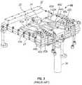
- FIG. 3is a perspective view of an ALD reactor, showing a gas distribution system
- FIG. 4is a perspective view of a portion of an ALD device, including a gas distribution system configured according to an embodiment
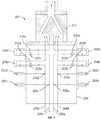
- FIG. 5is a schematic illustration of a gas distribution system, applicable to the device illustrated in FIG. 4 , showing connections among the paths for inert gas valving (IGV) functionality;
- IGVinert gas valving
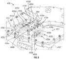
- FIG. 6is a perspective view of an ALD reactor having a gas distribution system configured according to another embodiment
- FIG. 7is a schematic illustration of the gas distribution system illustrated in FIG. 6 ;
- FIG. 8is a perspective view of an ALD reactor having a gas distribution system configured according to a further embodiment.
- FIG. 9is a perspective view of an ALD reactor having a gas distribution system configured according to a still further embodiment.
- FIG. 10is a flow chart generally illustrating a method for forming a thin film in accordance with one embodiment.
- the reactor and the gas lines leading to the reactorare typically contained within a vacuum chamber.
- the reactor, as well as the gas lines leading to the reactorshould be maintained at an appropriate temperature and often are heated. If the temperatures in the lines or reaction chamber are too low, condensation may occur and corrupt the ALD process. If the temperatures in the lines or reaction chamber are too high, the gases may degrade or decompose, which will also corrupt the ALD process.
- the gasesare continuously maintained at temperatures ranging from 50° C. to 650° C. or more.
- Such high temperature requirementscan limit the ability to use valves and filters in the gas lines in the vacuum chamber, particularly in the lines close to the reactor.
- Moving such components outside the ALD hot zonecan result in long pulse response times because of the distance between the source valve (outside the vacuum chamber) and the reactor, greater risk of diffusion of a reactant from a long line into the reactor between pulses of that reactant, long times required to purge the reactor of the previous reactant because of the lengths of gas lines between the source valve and the reactor, and increased potential for condensation of the precursor or reactant while it travels between the source valve and the reactor due to variations in temperature in longer gas lines.
- valves and/or filters to control the flow of precursors, reactants, and/or purge gasesare provided close to the reactor (for example, close to the inlet of the reaction chamber), so as to provide improved pulse response time, a faster reactor purge, reduced precursor consumption, and reduced potential for condensation of source material, and to allow for shorter delivery and/or backsuction lines.
- the valves and/or filtersare mounted over the reactor itself.
- the placement of valves and/or filters within a vacuum chamber surrounding the reaction chambercan reduce the space required to package such control hardware outside of the vacuum chamber, and can therefore reduce the space occupied by the overall ALD device.
- valves near the reactormay obviate separate valve heaters, as reaction chamber heaters can sufficiently heat the valves to prevent condensation.
- reaction chamber heaterscan sufficiently heat the valves to prevent condensation.
- the provision of filters within the vacuum chamber, downstream of any valvescan reduce the potential for particulate contamination on the substrate.
- ALDAtomic Layer Deposition
- ALDatomic layer deposition
- ALD type processesare based on controlled, self-limiting surface reactions of precursor chemicals. Gas phase reactions are avoided by feeding the precursors alternately and sequentially into the reaction chamber. Vapor phase reactants are separated from each other in the reaction chamber, for example, by removing excess reactants and/or reactant by-products from the reaction chamber between reactant pulses.
- a substrateis loaded into a reaction chamber and is heated to a suitable deposition temperature, generally at lowered pressure.
- Deposition temperaturesare maintained below the precursor thermal decomposition temperature but at a high enough level to avoid condensation of reactants and to provide the activation energy for the desired surface reactions.
- the appropriate temperature window for any given ALD reactionwill depend upon the surface termination and reactant species involved.
- a first reactantis conducted into the chamber in the form of vapor phase pulse and contacted with the surface of a substrate. Conditions are preferably selected such that no more than about one monolayer of the precursor is adsorbed on the substrate surface in a self-limiting manner. Excess first reactant and reaction byproducts, if any, are purged from the reaction chamber, often with a pulse of inert gas such as nitrogen or argon.
- Purging the reaction chambermeans that vapor phase precursors and/or vapor phase byproducts are removed from the reaction chamber such as by evacuating the chamber with a vacuum pump and/or by replacing the gas inside the reactor with an inert gas such as argon or nitrogen.
- Typical purging times for a single wafer reactorare from about 0.05 to 20 seconds, more preferably between about 1 and 10, and still more preferably between about 1 and 2 seconds.
- other purge timescan be utilized if necessary, such as when depositing layers over extremely high aspect ratio structures or other structures with complex surface morphology is needed, or when a high volume batch reactor is employed.
- the appropriate pulsing timescan be readily determined by the skilled artisan based on the particular circumstances.
- a second gaseous reactantis pulsed into the chamber where it reacts with the first reactant bound to the surface. Excess second reactant and gaseous by-products of the surface reaction are purged out of the reaction chamber, preferably with the aid of an inert gas. The steps of pulsing and purging are repeated until a thin film of the desired thickness has been formed on the substrate, with each cycle leaving no more than a molecular monolayer.
- Some ALD processescan have more complex sequences with three or more precursor pulses alternated, where each precursor contributes elements to the growing film. Reactants can also be supplied in their own pulses or with precursor pulses to strip or getter adhered ligands and/or free by-product, rather than contribute elements to the film.
- a binary filmcan be doped with a third element by infrequent addition of a third reactant pulse, e.g., every fifth cycle, in order to control stoichiometry of the film, and the frequency can change during the deposition in order to grade film composition.
- each pulse or phase of each cycleis preferably self-limiting.
- An excess of reactant precursorsis supplied in each phase to saturate the susceptible structure surfaces.
- Surface saturationensures reactant occupation of all available reactive sites (subject, for example, to physical size or “steric hindrance” restraints) and thus ensures excellent step coverage over any topography on the substrate.
- the degree of self-limiting behaviorcan be adjusted by, e.g., allowing some overlap of reactant pulses to trade off deposition speed (by allowing some CVD-type reactions) against conformality.
- Ideal ALD conditions with reactants well separated in time and spaceprovide near perfect self-limiting behavior and thus maximum conformality, but steric hindrance results in less than one molecular layer per cycle.
- Limited CVD reactions mixed with the self-limiting ALD reactionscan raise the deposition speed.
- suitable reactorsinclude commercially available ALD equipment such as the Pulsar® reactor, available from ASM America, Inc. of Phoenix, Ariz. Many other kinds of reactors capable of ALD growth of thin films can be employed, including CVD reactors equipped with appropriate equipment and means for pulsing the precursors. In some embodiments a flow type ALD reactor is used.
- the ALD processes described belowcan optionally be carried out in a reactor or reaction space connected to a cluster tool.
- a cluster toolbecause each reaction space is dedicated to one type of process, the temperature of the reaction space in each module can be kept constant, which improves the throughput compared to a reactor in which is the substrate is heated up to the process temperature before each run.
- a stand-alone reactorcan be equipped with a load-lock. In that case, it is not necessary to cool down the reaction space between each run.
- FIG. 1illustrates an ALD apparatus or tool 10 in which embodiments of the invention may be used.
- the illustrated ALD toolcomprises a cabinet 26 and an ALD device 20 .
- the cabinet 26may include a single cabinet or may include multiple cabinets coupled or connected together.
- the cabinet 26may be any shape or size desirable.
- a controller or control system 12 for controlling the ALD apparatus 10can be included inside or outside of the cabinet 26 .
- the control system 12can be any type of electrical system, processor, or the like which can be used to control the ALD process.
- control system 12includes an input device that allows a user of the ALD tool 10 to input information to cause the ALD tool 10 to perform various ALD processes, for example with different types of precursors and reactant gases, at different temperatures, different pulse durations and/or for a different number of cycles.
- the ALD device 20also includes a housing 22 in which a reactor 24 is disposed.
- FIG. 2is a cross-sectional view of the ALD device 20 shown in FIG. 1 , taken along line A-A of FIG. 1 .
- the housing 22surrounds or defines a vacuum chamber 28 , inside which the reactor 24 is disposed.
- the housing 22may be shaped in any way desired, and can be configured to contain devices for performing the ALD process, as well as contain the heat from the ALD process.
- the housing 22can include a rectangular box comprising a top, bottom and four sides.
- the top, bottom and four sides of the housing 22may include various openings in order to allow gas lines and/or other apparatuses entry or exit from the housing.
- the vacuum chamber 28can be an airtight container which is separate from the housing 22 , or can be an airtight enclosure formed by portions of the housing 22 .
- the housing 22can also be configured to withstand ALD process temperatures, which can range from about 50° C. to 650° C. or higher.
- the housing 22may have cooled walls and/or insulation to keep the temperature of at least the exterior of the housing 22 significantly below the temperature of the ALD process occurring within. Such a configuration can help prevent burns to operators and can also extend the life of attached systems, such as a control system, by keeping these systems at a lower temperature.
- the ALD device 20can include one or more heaters 30 configured to heat the interior of the housing 22 and any gas lines and other structures which may be disposed within the housing 22 .
- the heaters 30may be disposed at the top and/or the bottom of the housing 22 in such a manner as to maintain as constant a temperature as possible throughout the housing 22 .
- the heaters 30may be any type of heater that can operate at high temperatures suitable for ALD processes, including without limitation coiled resistance heaters and radiant heaters.
- a gas distribution system 60is disposed within the vacuum chamber 28 and connected to a mixer 34 .
- gases received from the gas distribution system 60are mixed before traveling through a diffuser or plenum 32 to the reactor 24 .
- ALDit may be desirable to mix one reactant with an inert carrier gas flow.
- ALD reactantsare not mixed in the gas phase, the fact that two ALD reactants sequentially flow through the same space in the mixer means than second reactants can react with first reactants which may have adhered on the internal surfaces of the mixer from the previous reactant pulse, causing deposition.
- Such controllable deposition, upstream of the reaction chamber,is preferred as a sacrificial reaction, as compared to allowing the first reactant to desorb from the reaction chamber surfaces during the second reactant pulse, which can lead to uncontrolled, non-self-limiting CVD-like reactions in the chamber, which can build much more quickly than ALD-like reactions.
- the mixer 34can then be periodically cleaned.
- the mixer 34has a smooth interior with no or very few and/or small discontinuities.
- the mixing devicecomprises a conical chamber in which the reactants enter at an angle with respect to the longitudinal axis of the chamber, causing the reactants to swirl around the inner conical surfaces and funnel to the reaction inlet channel 35 .
- An example of such a mixer 34 for ALDis described, e.g., in US Patent Publication No. 2005-0092247 A1.
- the diffuser 32can be configured to spread the gases horizontally and lead the gases downward into the reactor 24 .
- the inlet of the diffuserreceives gases from the gas distribution system and delivers a broadened flow to an inlet flange of the reaction chamber below for horizontal, laminar flow through the reaction chamber.
- the diffuser 32may be any shape that spreads the gases outward in a horizontal direction.
- a vacuum line 36can be connected to the reactor 24 to continually exhaust the reactor of flowing gases and/or to evacuate periodically between pulses.
- the gases used in the ALD processare supplied to the gas distribution system 60 from a gas supply system outside of the housing 22 .
- the precursor/reactant gasesmay be liquid, gas or solid at room temperature. Some gases used for ALD are naturally gaseous, while other reactants suitable for ALD processing are often liquid or solid at room temperature and atmospheric pressure and so are vaporized for processing. Conversion of each precursor/reactant into a gas can be performed outside of the housing 22 in a vaporizer vessel (not shown).
- the precursor/reactant gasescan be mixed with a carrier gas, which may be an inert gas such as nitrogen or argon, before entering the gas distribution system 60 .
- a single ALD apparatusmay have multiple sources of precursor, reactant and/or carrier gases, each of which may have its own gas line in the gas distribution system 60 .
- a first line of carrier gascan enter the vaporizer vessel in order to carry the precursor gas, while a second line (which may also be referred to as a bypass line) enters the housing 22 for use in other aspects of the ALD process (e.g., use as a purge gas).
- the gas distribution system 60includes an inert gas valving (IGV) arrangement, by which the flow or diffusion of each precursor/reactant from its source vessel to the reactor 24 through reactant conduits 40 a - d can be prevented by forming a gas phase barrier (also referred to as a diffusion barrier) of a gas (e.g., an inert gas) flowing in the opposite direction to the reactant flow in the conduit.
- a gas phase barrieralso referred to as a diffusion barrier
- an inert gas conduit 42 a - dConnected to each reactant conduit 40 a - d , upstream of the mixer 34 , is an inert gas conduit 42 a - d , through which an inert gas may be fed into its corresponding reactant conduit 40 a - d .
- a backsuction conduit 44 a - dis Also connected to each reactant conduit 40 a - d , upstream (relative to the reactant flow) of the connections to the inert gas conduits 42 a - d , is a backsuction conduit 44 a - d , each typically including a restrictor to prevent loss of reactant during reactant pulses. Backsuction may be applied through the backsuction conduit 44 a - d to create a reverse flow of inert gas through the section of its corresponding reactant conduit 40 a - d between the connections to the backsuction and inert gas conduits, and that reverse flow of inert gas serves as a diffusion barrier against continued reactant flow along the reactant conduit 40 a - d .
- the diffusion barriersi.e., the portions of the reactant conduits 40 a - d between the connection points for the inert gas conduits 42 a - d and the backsuction conduits 44 a - d
- the valves for creating the diffusion barriersi.e., the valves for controlling the inert gas and reactant gas flow, not illustrated in FIG. 3
- These valvescan also be used for separating the gas spaces of the precursor/reactant source vessels and the reactor 24 during evacuation of either or both of these components. Often these remote valves employ separate heaters to avoid reactant condensation, as they may be too remote from the reactor heaters 30 ( FIG. 2 ).
- the precursor/reactant, and carrier/purge gasesmust travel through long gas lines between their respective control valves (outside the vacuum chamber 28 ) and the mixer 34 .
- IGVinert gas valving
- these long gas linescan allow for variations in temperature and can also result in precipitate or decomposition of the gases, which can compromise the ALD process.
- a lot of precursoris trapped in those long lines with relatively high pressure, which the diffusion barrier is to stop. Long lines additionally effectively slow pulsing.
- the inert gas flow along the inert gas conduit 42 a - dis to be reduced to turn off the backward flow (diffusion barrier) and allow forward flow of reactant through the corresponding reactant conduit 40 a - d .
- a long inert gas line from the remote valves to the diffusion barrierdelays the time it takes for reduced inert gas flow to be effective and start the reactant pulse.
- FIG. 4illustrates an ALD device 100 including a gas distribution system 101 configured according to an embodiment of the present invention.
- the gas distribution system 101 of FIG. 4can be disposed relatively close to a downstream reactor 112 , such that a distance between control valve seats and the point at which different reactant flow paths merge to form a common flow path (e.g., to a common bore in a mixer, or to a diffuser) is in a range of about 5 mm to 150 mm, more preferably within about 10 mm to 100 mm, as measured along the gas flow paths.
- the positioning of the gas distribution systemcan also be such that the valves and reactor 112 share a common heating system, such as the reactor heaters 30 of FIG. 2 , without separate heaters or heater controls for the valves.
- the gas distribution system 101including valves, can be positioned along with the reactor 112 within a heated vacuum chamber inside the ALD device 100 , which may be configured in a similar manner to the ALD device illustrated in FIG. 2 .
- the gas distribution system 101includes two precursor/reactant gas valves 102 a and 102 b and an inert gas valve 104 mounted on a common manifold 106 .
- Each of the precursor/reactant valves 102 a and 102 bis configured to control a supply of a precursor (or reactant) gas to the manifold 106 .
- the inert gas valve 104is configured to control a supply of an inert gas (e.g., carrier or purge gas) to the manifold 106 .
- Also mounted on the manifold 106are two backsuction valves 108 a and 108 b , which are configured to control the application of suction to the manifold 106 .
- the manifold 106feeds into a diffuser 110 , which, in turn, feeds into a reactor 112 .
- the reactor 112is a horizontal flow reactor, such that the diffuser 110 feeds an inlet flange at the side of the reaction space within the reactor 112 to produce a laminar, horizontal flow of gases parallel and across the upper surface of the substrate.
- the gas distribution system 101including the valves 102 a , 102 b , 104 , 108 a , and 108 b , is mounted on or disposed directly above the reactor 112 , such that the distances are short and the gas distribution system 101 can be efficiently heated.
- the manifold 106is mounted to the diffuser 110 that leads directly into the reactor 112 .
- the manifold 106can also be mounted directly onto the reactor 112 .
- the precursor/reactant valves 102 a and 102 bare connected via supply lines 114 a and 114 b , respectively, to precursor or reactant sources (not shown), which can be disposed outside the ALD device 100 .
- the inert gas valve 104is connected via a supply line 116 to an inert gas source (not shown), which can also be disposed outside the ALD device 100 .
- the backsuction valves 108 a and 108 bare connected via lines 118 a and 118 b , respectively, to one or more vacuum sources (not shown), which can also be disposed outside the ALD device 100 .
- the lines 114 a , 114 b , 116 , 118 a , and 118 bmay comprise any type of piping or tubing that can withstand the temperatures to which they will be heated inside the vacuum chamber.
- the lines 114 a , 114 b , 116 , 118 a , and 118 bcan also be formed of a material which will not react with the gases flowing through them.
- valves 102 a , 102 b , 104 , 108 a , and 108 bcan be configured to operate at very high speeds, with open/close times in the microsecond range, e.g., 5-100 ms, preferably 5-10 ms.
- the valves 102 a , 102 b , 104 , 108 a , and 108 bcan also be configured to operate at temperatures up to 220° C. or higher.
- the number of precursor/reactant valves 102 a , 102 b , inert gas valves 104 , and backsuction valves 108 a , 108 bcan vary in embodiments, depending on the particular application and the desired processing capability of the ALD system.
- an ALD systemincludes at least two reactants and gas distribution therefor, and three- and four-reactant systems are not uncommon.
- the valves 102 a , 102 b , 104 , 108 a , and 108 bmay be any type of valve that can withstand high temperatures.
- Valves 102 a , 102 b , 104 , 108 a , and 108 bmay be ball valves, butterfly valves, check valves, gate valves, piezoelectric valves, globe valves or the like. Metal diaphragm valves may also be used, and may be preferred for a high temperature environment.
- the valves 102 a , 102 b , 104 , 108 a , and 108 bcan be pneumatically actuated valves.
- the valves 102 a , 102 b , 104 , 108 a , and 108 bmay be formed from any material that will function at the high temperatures required for ALD processing, such as 316L stainless steel and the like.
- Some embodimentssuch as an ALD system configured for alumina deposition, can include valves configured to operate up to 220° C. Still other embodiments can include valves configured to operate at temperatures up to 400° C., or at even higher temperatures.
- the reactant and backsuction valves in each of the embodiments described hereinneed not be leak tight when “closed” due to the operation of IGV. Rather, the reaction and backsuction valves may be leaky or non-fully closing, as disclosed in U.S. Patent Publication No. 2010-0266765 A1, published on Oct. 21, 2010, the entire disclosure of which is incorporated herein by reference.
- valvesneed not fully close in the offstate, while inert gas valving still cleanly cuts off reactant flow between reactant pulses by way of a diffusion barrier, degradation of the valves within the hot zone is of less concern.
- reactant lossescan be reduced by controlling relative flow through the backsuction lines at different points in the process, relative to fixed restrictors on the backsuction lines as more commonly used for IGV.
- the valvesmay be fully closing.
- valves 102 a , 102 b , 104 , 108 a , and 108 bcan be surface-mount valves.
- fixed orificescan also be disposed between the backsuction valves 108 a and 108 b , respectively, and the manifold 106 , as shown and discussed below with respect to FIG. 5B .
- the provision of fixed orificescan be useful in controlling backsuction of residual precursors or reactants to the vacuum source.
- the manifold 106can include a mixer for mixing, e.g., a reactant flow from one source (e.g., including reactant and inert carrier gases) with inert gas flow from another source during operation.
- a reactant flow from one sourcee.g., including reactant and inert carrier gases
- the manifold 106includes a conical chamber, with gases (e.g., precursor/reactant gases and carrier/purge gases) entering at an angle with respect to the longitudinal axis of the chamber, causing the gases to swirl around the inner conical surfaces and funnel to the diffuser 106 .
- gasese.g., precursor/reactant gases and carrier/purge gases
- FIG. 5is a schematic illustration of one manner of configuring the gas distribution system 101 illustrated in FIG. 4 for inert gas valving (IGV).
- FIG. 5shows the flow paths for only one reactant; the skilled artisan will readily appreciate that a similar structure is provided for each additional reactant (two total shown in FIG. 4 , but additional reactants can be added).
- the precursor/reactant valve 102 a , inert gas valve 104 , and the backsuction valve 108 aare in fluid communication with the interior of the manifold 106 via short passageways 122 a , 124 , and 126 a , respectively, which passageways can extend through the body of the manifold 106 to reach a central bore.
- FIG. 5shows the position of a gas diffusion barrier 128 within the manifold 106 . As described below, the gas diffusion barrier 128 forms between pulses of the reactant.
- a first precursor/reactant gas valve 102 acan be opened to allow the gas to travel through its corresponding line 122 a and into the manifold 106 .
- the precursor/reactant gas(or precursor/reactant and carrier gas mixture) then travels through the diffuser 110 and into the reactor 112 .
- the valve 102 acan be closed to restrict the flow of the precursor/reactant gas.
- the backsuction valve 108 acan be opened to apply backsuction to the manifold 106 through the line 126 a and thereby cause a backward flow along the reactant path from the inert gas source to the junction with the backsuction line, as illustrated by the diffusion barrier 128 in FIG. 5 .
- the inert gas valve 104can be open throughout the entire cycle, to allow the inert gas into the manifold 106 to act as a carrier gas for each precursor or reactant gas during precursor/reactant pulses, as well as a purge gas between precursor/reactant pulses. This cycle can be then repeated with the second precursor/reactant gas valve 102 b and backsuction valve 108 b ( FIG. 4 ). The entire process can be repeated in order to build up a layer of a desired thickness on the substrate in the reactor.
- backsuction valves 108 a , 108 b and IGV functionalitymay not be included, and instead longer periods of purging with inert gas can be used to control a purge cycle in which the inert gas is used to force any non-reacted gases and any gaseous reaction byproducts through and out of the reactor.
- Locating such valves 102 a , 102 b , 104 , 108 a , and 108 b within the vacuum chamber and/or mounted close to the inlet of the reactor 112can eliminate the need to separately heat the valves farther upstream of the reactor 112 , or outside the vacuum chamber, as heating of the reactor 112 may be sufficient to also heat the valves sufficiently to avoid condensation.
- embodimentscan provide improved valve pulse response time, as well as the time required between cycles.
- Embodimentscan also reduce the use (and waste) of precursor and reactant gases, at least in part due to the fact that there is a smaller volume of gas between the respective valves and the reactor. Even less waste can be achieved during reactant pulses by use of controlled valves, even if not gas tight, on the suction line rather than restrictors alone. Further, embodiments can reduce the delivery line surface area to which the precursor and reactant gases are exposed after leaving their respective valves, reducing the risk of decomposition or condensation in the delivery lines.
- FIGS. 6 and 7illustrate an ALD device 200 including a gas distribution system 201 configured according to another embodiment.
- the gas distribution system 201 of FIG. 6can be disposed within a heated vacuum chamber inside the ALD device 200 , which may be configured in a similar manner to the ALD device illustrated in FIG. 2 .
- the gas distribution system 201need not be within a vacuum chamber, but sits sufficiently close to a downstream ALD reactor 216 as to be heated by the reactor's heating system and avoid reactant condensation, without any separate heating system for the illustrated components of the gas distribution system 201 .
- a distance between control valve seats and the point at which different reactant flow paths merge to form a common flow pathis in a range of about 5 mm to 150 mm, more preferably within about 10 mm to 100 mm, as measured along the gas flow paths.
- the positioning of the gas distribution systemcan also be such that the valves and reactor 216 share a common heating system, such as the reactor heaters 30 of FIG. 2 , without separate heaters or heater controls for the valves.
- the gas distribution system 201includes four precursor/reactant gas lines 202 a - d connected to a common manifold 204 .
- Each precursor/reactant gas line 202 a - dhas a corresponding backsuction line 206 a - d which is also connected to the common manifold 204 .
- each precursor/reactant gas line 202 a - dhas a corresponding filter 208 a - d which is mounted on the common manifold 204 .
- Each precursor/reactant gas line 202 a - dalso has a corresponding inert gas line 210 a - d , each of which connects with its corresponding precursor/reactant gas line 202 a - d , upstream of its corresponding filter 208 a - d and downstream of its connection to its corresponding backsuction line 206 a - d .
- Downstream and upstreamassume flow toward the reactor 216 for purpose of establishing directions.
- the interior of the manifold 204leads to a mixer 212 , which funnels gases into a diffuser 214 . As can be seen in FIG.
- the manifold 204along with the precursor/reactant gas lines 202 a - d , the backsuction lines 206 a - d , the filters 208 a - d , and the inert gas lines 210 a - d are all connected to the manifold 204 in close proximity to (and, in this embodiment, mounted to and directly above) the reactor 216 .
- the manifold 204is mounted by way of the mixer 212 to the diffuser 214 that leads directly into the reactor 216 .
- the manifold 204can also be mounted directly onto the reactor 216 .
- the precursor/reactant gas lines 202 a - dare connected to precursor or reactant sources (not shown).
- the inert gas lines 210 a - dare connected to an inert gas source (not shown), which can also be disposed outside the ALD device 200 .
- the backsuction lines 206 a - dare connected to one or more vacuum sources (not shown), which can also be disposed outside the ALD device 200 .
- One or more valvescan be disposed outside the ALD device 200 and configured to control the supply of precursor/reactant or inert gas to the precursor/reactant gas lines 202 a - d and the inert gas lines 210 a - d , respectively.
- One or more additional valvescan be disposed outside the ALD device 200 and configured to control the application of suction on the backsuction lines 206 a - d .
- the lines 202 a - d , 206 a - d , and 210 a - dmay comprise any type of piping or tubing that can withstand the temperatures to which they will be heated inside the vacuum chamber or otherwise commonly heated with the reactor 216 .
- the lines 202 a - d , 206 a - d , and 210 a - dcan also be formed of a material which will not react with the gases flowing through them.
- the number of precursor/reactant lines 202 a - d , inert gas lines 210 a - d , backsuction lines 206 a - d , and filters 208 a - dcan vary in embodiments, depending on the particular application and the desired processing capability of the ALD system.
- the filters 208 a - dcan be configured to prevent particles from traveling from the upstream gas lines 202 a - d and 210 a - d into the reactor 216 .
- the manifold 204as well as the filters 208 a - d attached to the manifold 204 , can be heated to a temperature close or equal to the temperature of the reactor 216 so as to limit or prevent condensation of vapors, at least within or downstream of the filters 208 a - d .
- the filters 208 a - dcan be any type of filter that can withstand high temperatures, such as, for example, high purity porous metal (e.g., sintered metal) media or porous ceramic filters.
- the filters 208 a - dcan be surface-mount filters which are positioned on the manifold 204 in very close proximity to point of entry of the reactant/precursors to the mixer 212 .
- the use of surface-mount filterscan enable a much smaller, more compact arrangement of gas or vapor delivery components as compared to conventional systems, allowing their placement within the heated vacuum chamber or hot zone in which the reactor 216 is disposed.
- Positioning the filters 208 a - d within the heated vacuum chambercan make the performance of the ALD device 200 less sensitive to temperature variations within the gas lines and can also obviate separate heaters for the filters, as the heaters for the reactor 216 and/or outer vacuum chamber can sufficiently heat the filters.
- FIG. 7is a schematic illustration of the gas distribution system 201 illustrated in FIG. 6 .
- the backsuction lines 206 a - dare in fluid communication with corresponding precursor/reactant gas lines 202 a - d at points 220 a - d within the manifold 204 , upstream of points 222 a - d where the inert gas lines 210 a - d join with the precursor/reactant gas lines 202 a - d .
- the filters 208 a - dare located downstream, relative to the direction of reactant flow, of the points 222 a - d.
- a first precursor/reactant gas valve(not shown) can be opened to allow the gas to travel through its corresponding line 202 a and into the manifold 204 .
- an inert gas valve(not shown) can be opened at the same time or kept open to allow the inert gas into the manifold 204 through inert gas line 210 a , to act as a carrier gas for the precursor or reactant gas or to prevent contamination of the inert gas line 201 a with stagnant precursor.
- the precursor/reactant gas(or precursor/reactant and carrier gas mixture) then travels through the filter 202 a , into the mixer 212 , and then into the reactor 216 ( FIG. 6 ).
- the precursor/reactant gas valve controlling line 202 acan be closed to restrict the flow of the precursor/reactant gas.
- inert gas flowis increased or reestablished through line 210 a
- backsuctionis applied to line 206 a to create a reverse flow of gas between the connection points 222 a and 220 a , thereby creating a diffusion barrier and preventing any reactant from diffusing forward (i.e., from line 202 a toward the manifold 204 ).
- Additional inert gas that is not drawn into the backsuction linecan purge the reactor 216 of any remaining precursor/reactant gas (and/or byproduct).
- This cyclecan be then repeated with second, third, and fourth precursor/reactant gases in lines 202 b - d , respectively, and their corresponding inert gas lines 210 b - d and backsuction lines 206 b - d .
- the entire processcan be repeated as desired in order to build up a layer of a desired thickness on the substrate in the reactor 216 .
- backsuction lines 206 a - dmay not be included, and instead the inert gas lines 210 a - d can be used to control purge cycles in which the inert gas is used to force any non-reacted gases and any gaseous reaction byproducts through and out of the reactor 216 , without creating a diffusion barrier.
- FIG. 8illustrates an ALD device 300 including a gas distribution system 301 configured according to still another embodiment.
- the gas distribution system 301 of FIG. 8can be disposed within a heated vacuum chamber (not shown) inside the ALD device 300 , which may be configured in a similar manner to the ALD device illustrated in FIG. 2 .
- the gas distribution system 301need not be within a vacuum chamber, but sits sufficiently close to a downstream ALD reactor 326 as to be heated by the reactor's heating system and avoid reactant condensation, without any separate heating system for the illustrated components of the gas distribution system 301 .
- a distance between control valve seats and the point at which different reactant flow paths merge to form a common flow pathis in a range of about 5 mm to 150 mm, more preferably within about 10 mm to 100 mm, as measured along the gas flow paths.
- the positioning of the gas distribution systemcan also be such that the valves and reactor 326 share a common heating system, such as the reactor heaters 30 of FIG. 2 , without separate heaters or heater controls for the valves.
- the gas distribution system 301includes four precursor/reactant gas lines 302 a - d which are connected, through various other components, to a common manifold 304 .
- Each precursor/reactant gas line 302 a - dhas a corresponding filter 306 a - d through which the gas passes as it travels toward the manifold 304 .
- Downstream of each filter 306 a - dis a corresponding precursor/reactant gas valve 308 a - d , which controls the flow of precursor/reactant gas from the filter 306 a - d to a backsuction valve 312 a - d .
- the precursor/reactant gas valves 308 a - dcan be two-port valves, with one port connected to an outlet of each filter 306 a - d , and with the other port connected to a first port of the corresponding backsuction valve 312 a - d . Downstream of each backsuction valve 312 a - d is a corresponding inert gas valve 314 a - d .
- the backsuction valves 312 a - dcan be three-port valves, with a second port connected to a first port of a corresponding inert gas valve 314 a - d , and with a third port connected to a corresponding backsuction line 310 a - d .
- the inert gas valves 314 a - dcan also be three-port valves, with a second port in fluid communication with the manifold 304 , and with a third port connected to a corresponding inert gas supply line 316 a - d .
- the inert gas valves 314 a - dcan connect with the manifold 304 through corresponding connecting lines 318 a - d , as shown in FIG. 8 , or they can be mounted directly on the manifold 304 .
- the manifold 304is mounted by way of a mixer 320 to a diffuser 322 that leads directly into the reactor 325 .
- the manifold 304can also be mounted directly onto the reactor 326 .
- the precursor/reactant gas lines 302 a - dare connected to precursor or reactant sources (not shown).
- the inert gas supply lines 316 a - dare connected to one or more inert gas sources (not shown), which can also be disposed outside the ALD device 300 .
- the backsuction lines 310 a - dare connected to one or more vacuum sources (not shown), which can also be disposed outside the ALD device 300 .
- a first precursor/reactant gas valve 308 acan be opened to allow the gas to travel from its corresponding line 302 a , through the filter 306 a , and through the backsuction valve 312 a .
- the port of the backsuction valve 312 a that is connected to the backsuction line 310 acan be closed while the other two ports remain open, so that the precursor/reactant gas can pass through the valve 312 a to the inert gas valve 314 a .
- the three-port inert gas valve 314 acan have at least two ports open, so as to allow the precursor/reactant gas to pass through the valve 314 a , to the connecting line 318 a and into the manifold 204 .
- the port of the inert gas valve 314 a that is connected to the inert gas supply line 316 acan be open at the same time, so as to allow inert gas to flow into the connecting line 318 a along with the precursor/reactant gas.
- the precursor/reactant gas(or precursor/reactant and inert gas mixture) then travels through the manifold 304 , into the mixer 320 , and then into the diffuser 322 and thence into a reactor 326 upon which the gas distribution system 301 is mounted.
- the precursor/reactant gas valve 308 acan be closed to restrict the flow of the precursor/reactant gas.
- the port of the backsuction valve 312 a which is connected to the backsuction line 310 acan be opened to create a reverse flow of gas, from the inert gas valve 314 a toward the backsuction valve 312 a , thereby creating a diffusion barrier and preventing any reactant from diffusing forward (i.e., toward the manifold 304 ).
- Additional inert gas that is not drawn into the backsuction linecan purge the reactor 326 of any remaining precursor/reactant gas (and/or byproduct).
- This pulse sequencecan be then repeated with second, third, and fourth precursor/reactant gas valves 306 b - d for lines 302 b - d , respectively, and their corresponding inert gas valves 312 b - d and backsuction valves 314 b - d , as called for by the ALD recipe for each cycle.
- an ALD recipemay employ two, three, four or more reactants or precursors per cycle, pulses of which are generally (but not necessarily) separated by a purging stage.
- the entire processcan be repeated as desired in order to build up a layer of a desired thickness on the substrate in the reactor 326 .
- the skilled artisanwill also appreciate that not every cycle in a given ALD process is necessarily identical with all other cycles in the process, and changes may be made to tailor composition and profile of the thin film being deposited.
- one or more of the backsuction valvescan be cycled between two levels of flow coefficients.
- a valve 312 a - din a first state, can have a relatively higher flow coefficient, while in a second state, the valve 312 a - d can have a relatively lower flow coefficient, comparable to the fixed restrictors used in inert gas valving arrangements.
- the first statecan be a fully open position
- the second statecan be an almost closed position.
- the first statecan be used to more rapidly stop a precursor/reactant pulse (by rapidly creating the diffusion barrier using a large backsuction flow enabled by the higher flow coefficient), while the second state can be used during precursor/reactant pulsing to reduce precursor/reactant waste through the backsuction lines (using a low backsuction flow enabled by the lower flow coefficient).
- the time to reverse flow in the diffusion barrier zonecan be reduced compared to use of a fixed restrictor by increasing backsuction between precursor/reactant pulses (i.e., the inert gas valving turns on faster).
- the chemical waste of precursor/reactant to process exhaustcan be reduced during precursor/reactant pulsing since backsuction flow is very low.
- backsuction valves 314 a - dmay not be included, and instead the inert gas valves 312 a - d can be used to control purge cycles in which the inert gas is used to force any non-reacted gases and any gaseous reaction byproducts through and out of the reactor 326 , without inert gas valving.
- FIG. 9illustrates an ALD device 400 including a gas distribution system 401 configured according to further embodiment.
- the gas distribution system 401 of FIG. 9can be mounted on a reactor 412 and disposed within a heated vacuum chamber (not shown) inside the ALD device 400 , which may be configured in a similar manner to the ALD device illustrated in FIG. 2 .
- the gas distribution system 401need not be within a vacuum chamber, but sits sufficiently close to the downstream ALD reactor 412 as to be heated by the reactor's heating system and avoid reactant condensation, without any separate heating system for the illustrated components of the gas distribution system 401 .
- a distance between control valve seats and the point at which different reactant flow paths merge to form a common flow pathis in a range of about 5 mm to 150 mm, more preferably within about 10 mm to 100 mm, as measured along the gas flow paths.
- the positioning of the gas distribution systemcan also be such that the valves and reactor 412 share a common heating system, such as the reactor heaters 30 of FIG. 2 , without separate heaters or heater controls for the valves.
- the gas distribution system 401is configured in a similar manner to the gas distribution system 201 shown in FIG. 6 , except that the system 401 includes four precursor/reactant gas valves 403 a - d configured to control the flow of each precursor/reactant gas from its corresponding precursor/reactant gas line 402 a - d to its corresponding filter 408 a - d and ultimately to the manifold 404 .
- Backsuction lines 406 a - dalso connect to the valves 403 a - d .
- inert gas lines 410 a - dconnect each with each precursor/reactant gas line 402 a - d , downstream of the valves 403 a - d but upstream of the filters 408 a - d .
- the manifold 404is mounted by way of a mixer to a diffuser that leads directly into the reactor 412 .
- the manifold 404can also be mounted directly onto the reactor 412 .
- FIG. 10is a flow chart generally illustrating a method 500 for forming a thin film in accordance with one embodiment.
- a vapor phase pulse of a first precursor/reactantcan be provided to the reaction chamber.
- any excess of the first precursor/reactantcan be removed from the reaction chamber.
- a vapor phase pulse of a second precursor/reactantcan be provided to the reaction chamber.
- any excess of the second precursor/reactant(along with any reaction byproducts, if any) can be removed from the reaction chamber.
- Blocks 502 - 508can together be referred to as a deposition cycle, and of course the cycle can include additional pulses of additional precursors or reactants.
- the deposition cyclecan be repeated until a film of a desired thickness is formed.
- the process 500can be controlled by a control system, as described above for the controller or control system 12 of FIG. 1 , which may include a computer having one or more processors executing control programming information (e.g., defining the sequence and parameters of each precursor, reactant, and purge step) stored in memory.
- control programming informatione.g., defining the sequence and parameters of each precursor, reactant, and purge step
- precursors/reactantscan be removed from the reaction chamber by stopping the flow of a precursor/reactant while purging the chamber, e.g., by continuing the flow of an inert carrier gas such as nitrogen or argon.
- the removal stepcan include supplying an inert gas to the precursor/reactant line at a connection point upstream of the point of entry into the reaction chamber, and applying backsuction to the precursor/reactant line upstream (relative to the reactant flow) of the connection point.
- Applying backsuction to the precursor/reactant line in such a configurationcan create a reverse flow of precursor/reactant through the section of the precursor/reactant line between the connection to the backsuction and the connection to the inert gas supply, thereby creating a diffusion barrier and preventing any precursor/reactant from diffusing forward (i.e., toward the reaction chamber) between precursor/reactant pulses.
Landscapes
- Chemical & Material Sciences (AREA)
- General Chemical & Material Sciences (AREA)
- Chemical Kinetics & Catalysis (AREA)
- Engineering & Computer Science (AREA)
- Materials Engineering (AREA)
- Mechanical Engineering (AREA)
- Metallurgy (AREA)
- Organic Chemistry (AREA)
- Chemical Vapour Deposition (AREA)
Abstract
Description
Claims (22)
Priority Applications (1)
| Application Number | Priority Date | Filing Date | Title |
|---|---|---|---|
| US15/177,210US11208722B2 (en) | 2011-12-27 | 2016-06-08 | Vapor flow control apparatus for atomic layer deposition |
Applications Claiming Priority (2)
| Application Number | Priority Date | Filing Date | Title |
|---|---|---|---|
| US13/337,604US9388492B2 (en) | 2011-12-27 | 2011-12-27 | Vapor flow control apparatus for atomic layer deposition |
| US15/177,210US11208722B2 (en) | 2011-12-27 | 2016-06-08 | Vapor flow control apparatus for atomic layer deposition |
Related Parent Applications (1)
| Application Number | Title | Priority Date | Filing Date |
|---|---|---|---|
| US13/337,604DivisionUS9388492B2 (en) | 2011-12-27 | 2011-12-27 | Vapor flow control apparatus for atomic layer deposition |
Publications (2)
| Publication Number | Publication Date |
|---|---|
| US20160281232A1 US20160281232A1 (en) | 2016-09-29 |
| US11208722B2true US11208722B2 (en) | 2021-12-28 |
Family
ID=48653309
Family Applications (2)
| Application Number | Title | Priority Date | Filing Date |
|---|---|---|---|
| US13/337,604Active2034-07-25US9388492B2 (en) | 2011-12-27 | 2011-12-27 | Vapor flow control apparatus for atomic layer deposition |
| US15/177,210Active2033-03-17US11208722B2 (en) | 2011-12-27 | 2016-06-08 | Vapor flow control apparatus for atomic layer deposition |
Family Applications Before (1)
| Application Number | Title | Priority Date | Filing Date |
|---|---|---|---|
| US13/337,604Active2034-07-25US9388492B2 (en) | 2011-12-27 | 2011-12-27 | Vapor flow control apparatus for atomic layer deposition |
Country Status (1)
| Country | Link |
|---|---|
| US (2) | US9388492B2 (en) |
Cited By (2)
| Publication number | Priority date | Publication date | Assignee | Title |
|---|---|---|---|---|
| US11371146B2 (en)* | 2019-04-25 | 2022-06-28 | Beneq Oy | Gas distribution unit in connection with ALD reactor |
| US11459657B2 (en)* | 2019-03-06 | 2022-10-04 | Ckd Corporation | Gas supply unit and gas supply method |
Families Citing this family (385)
| Publication number | Priority date | Publication date | Assignee | Title |
|---|---|---|---|---|
| US8152922B2 (en)* | 2003-08-29 | 2012-04-10 | Asm America, Inc. | Gas mixer and manifold assembly for ALD reactor |
| US10378106B2 (en) | 2008-11-14 | 2019-08-13 | Asm Ip Holding B.V. | Method of forming insulation film by modified PEALD |
| US9394608B2 (en) | 2009-04-06 | 2016-07-19 | Asm America, Inc. | Semiconductor processing reactor and components thereof |
| US8802201B2 (en) | 2009-08-14 | 2014-08-12 | Asm America, Inc. | Systems and methods for thin-film deposition of metal oxides using excited nitrogen-oxygen species |
| US9312155B2 (en) | 2011-06-06 | 2016-04-12 | Asm Japan K.K. | High-throughput semiconductor-processing apparatus equipped with multiple dual-chamber modules |
| US10364496B2 (en) | 2011-06-27 | 2019-07-30 | Asm Ip Holding B.V. | Dual section module having shared and unshared mass flow controllers |
| US10854498B2 (en) | 2011-07-15 | 2020-12-01 | Asm Ip Holding B.V. | Wafer-supporting device and method for producing same |
| US20130023129A1 (en) | 2011-07-20 | 2013-01-24 | Asm America, Inc. | Pressure transmitter for a semiconductor processing environment |
| US9017481B1 (en) | 2011-10-28 | 2015-04-28 | Asm America, Inc. | Process feed management for semiconductor substrate processing |
| US9574268B1 (en) | 2011-10-28 | 2017-02-21 | Asm America, Inc. | Pulsed valve manifold for atomic layer deposition |
| US9388492B2 (en)* | 2011-12-27 | 2016-07-12 | Asm America, Inc. | Vapor flow control apparatus for atomic layer deposition |
| US9558931B2 (en) | 2012-07-27 | 2017-01-31 | Asm Ip Holding B.V. | System and method for gas-phase sulfur passivation of a semiconductor surface |
| US9659799B2 (en) | 2012-08-28 | 2017-05-23 | Asm Ip Holding B.V. | Systems and methods for dynamic semiconductor process scheduling |
| US9021985B2 (en) | 2012-09-12 | 2015-05-05 | Asm Ip Holdings B.V. | Process gas management for an inductively-coupled plasma deposition reactor |
| US10714315B2 (en) | 2012-10-12 | 2020-07-14 | Asm Ip Holdings B.V. | Semiconductor reaction chamber showerhead |
| US20160376700A1 (en) | 2013-02-01 | 2016-12-29 | Asm Ip Holding B.V. | System for treatment of deposition reactor |
| US9484191B2 (en) | 2013-03-08 | 2016-11-01 | Asm Ip Holding B.V. | Pulsed remote plasma method and system |
| US9589770B2 (en) | 2013-03-08 | 2017-03-07 | Asm Ip Holding B.V. | Method and systems for in-situ formation of intermediate reactive species |
| US8993054B2 (en) | 2013-07-12 | 2015-03-31 | Asm Ip Holding B.V. | Method and system to reduce outgassing in a reaction chamber |
| US9240412B2 (en) | 2013-09-27 | 2016-01-19 | Asm Ip Holding B.V. | Semiconductor structure and device and methods of forming same using selective epitaxial process |
| US9605343B2 (en) | 2013-11-13 | 2017-03-28 | Asm Ip Holding B.V. | Method for forming conformal carbon films, structures conformal carbon film, and system of forming same |
| SG11201605901QA (en)* | 2014-01-23 | 2016-08-30 | Ultratech Inc | Vapor delivery system |
| US10683571B2 (en) | 2014-02-25 | 2020-06-16 | Asm Ip Holding B.V. | Gas supply manifold and method of supplying gases to chamber using same |
| US10167557B2 (en) | 2014-03-18 | 2019-01-01 | Asm Ip Holding B.V. | Gas distribution system, reactor including the system, and methods of using the same |
| US11015245B2 (en) | 2014-03-19 | 2021-05-25 | Asm Ip Holding B.V. | Gas-phase reactor and system having exhaust plenum and components thereof |
| US10858737B2 (en) | 2014-07-28 | 2020-12-08 | Asm Ip Holding B.V. | Showerhead assembly and components thereof |
| US9890456B2 (en) | 2014-08-21 | 2018-02-13 | Asm Ip Holding B.V. | Method and system for in situ formation of gas-phase compounds |
| US10941490B2 (en) | 2014-10-07 | 2021-03-09 | Asm Ip Holding B.V. | Multiple temperature range susceptor, assembly, reactor and system including the susceptor, and methods of using the same |
| US9657845B2 (en) | 2014-10-07 | 2017-05-23 | Asm Ip Holding B.V. | Variable conductance gas distribution apparatus and method |
| KR102300403B1 (en) | 2014-11-19 | 2021-09-09 | 에이에스엠 아이피 홀딩 비.브이. | Method of depositing thin film |
| US20160168699A1 (en)* | 2014-12-12 | 2016-06-16 | Asm Ip Holding B.V. | Method for depositing metal-containing film using particle-reduction step |
| KR102263121B1 (en) | 2014-12-22 | 2021-06-09 | 에이에스엠 아이피 홀딩 비.브이. | Semiconductor device and manufacuring method thereof |
| US10529542B2 (en) | 2015-03-11 | 2020-01-07 | Asm Ip Holdings B.V. | Cross-flow reactor and method |
| US10276355B2 (en) | 2015-03-12 | 2019-04-30 | Asm Ip Holding B.V. | Multi-zone reactor, system including the reactor, and method of using the same |
| US10458018B2 (en) | 2015-06-26 | 2019-10-29 | Asm Ip Holding B.V. | Structures including metal carbide material, devices including the structures, and methods of forming same |
| US10600673B2 (en) | 2015-07-07 | 2020-03-24 | Asm Ip Holding B.V. | Magnetic susceptor to baseplate seal |
| US10043661B2 (en) | 2015-07-13 | 2018-08-07 | Asm Ip Holding B.V. | Method for protecting layer by forming hydrocarbon-based extremely thin film |
| US10083836B2 (en) | 2015-07-24 | 2018-09-25 | Asm Ip Holding B.V. | Formation of boron-doped titanium metal films with high work function |
| US10087525B2 (en) | 2015-08-04 | 2018-10-02 | Asm Ip Holding B.V. | Variable gap hard stop design |
| US9647114B2 (en) | 2015-08-14 | 2017-05-09 | Asm Ip Holding B.V. | Methods of forming highly p-type doped germanium tin films and structures and devices including the films |
| US9960072B2 (en) | 2015-09-29 | 2018-05-01 | Asm Ip Holding B.V. | Variable adjustment for precise matching of multiple chamber cavity housings |
| US10211308B2 (en) | 2015-10-21 | 2019-02-19 | Asm Ip Holding B.V. | NbMC layers |
| US10322384B2 (en) | 2015-11-09 | 2019-06-18 | Asm Ip Holding B.V. | Counter flow mixer for process chamber |
| US9627221B1 (en) | 2015-12-28 | 2017-04-18 | Asm Ip Holding B.V. | Continuous process incorporating atomic layer etching |
| US11139308B2 (en) | 2015-12-29 | 2021-10-05 | Asm Ip Holding B.V. | Atomic layer deposition of III-V compounds to form V-NAND devices |
| US10529554B2 (en) | 2016-02-19 | 2020-01-07 | Asm Ip Holding B.V. | Method for forming silicon nitride film selectively on sidewalls or flat surfaces of trenches |
| US10468251B2 (en) | 2016-02-19 | 2019-11-05 | Asm Ip Holding B.V. | Method for forming spacers using silicon nitride film for spacer-defined multiple patterning |
| US10501866B2 (en) | 2016-03-09 | 2019-12-10 | Asm Ip Holding B.V. | Gas distribution apparatus for improved film uniformity in an epitaxial system |
| US10343920B2 (en) | 2016-03-18 | 2019-07-09 | Asm Ip Holding B.V. | Aligned carbon nanotubes |
| US9892913B2 (en) | 2016-03-24 | 2018-02-13 | Asm Ip Holding B.V. | Radial and thickness control via biased multi-port injection settings |
| US10087522B2 (en) | 2016-04-21 | 2018-10-02 | Asm Ip Holding B.V. | Deposition of metal borides |
| US10190213B2 (en) | 2016-04-21 | 2019-01-29 | Asm Ip Holding B.V. | Deposition of metal borides |
| US10865475B2 (en) | 2016-04-21 | 2020-12-15 | Asm Ip Holding B.V. | Deposition of metal borides and silicides |
| US10367080B2 (en) | 2016-05-02 | 2019-07-30 | Asm Ip Holding B.V. | Method of forming a germanium oxynitride film |
| US10032628B2 (en) | 2016-05-02 | 2018-07-24 | Asm Ip Holding B.V. | Source/drain performance through conformal solid state doping |
| KR102592471B1 (en) | 2016-05-17 | 2023-10-20 | 에이에스엠 아이피 홀딩 비.브이. | Method of forming metal interconnection and method of fabricating semiconductor device using the same |
| US11453943B2 (en) | 2016-05-25 | 2022-09-27 | Asm Ip Holding B.V. | Method for forming carbon-containing silicon/metal oxide or nitride film by ALD using silicon precursor and hydrocarbon precursor |
| US10662527B2 (en) | 2016-06-01 | 2020-05-26 | Asm Ip Holding B.V. | Manifolds for uniform vapor deposition |
| JP6696322B2 (en)* | 2016-06-24 | 2020-05-20 | 東京エレクトロン株式会社 | Gas processing apparatus, gas processing method and storage medium |
| US10388509B2 (en) | 2016-06-28 | 2019-08-20 | Asm Ip Holding B.V. | Formation of epitaxial layers via dislocation filtering |
| US9859151B1 (en) | 2016-07-08 | 2018-01-02 | Asm Ip Holding B.V. | Selective film deposition method to form air gaps |
| US10612137B2 (en) | 2016-07-08 | 2020-04-07 | Asm Ip Holdings B.V. | Organic reactants for atomic layer deposition |
| US9793135B1 (en) | 2016-07-14 | 2017-10-17 | ASM IP Holding B.V | Method of cyclic dry etching using etchant film |
| US10714385B2 (en) | 2016-07-19 | 2020-07-14 | Asm Ip Holding B.V. | Selective deposition of tungsten |
| KR102354490B1 (en) | 2016-07-27 | 2022-01-21 | 에이에스엠 아이피 홀딩 비.브이. | Method of processing a substrate |
| US9812320B1 (en) | 2016-07-28 | 2017-11-07 | Asm Ip Holding B.V. | Method and apparatus for filling a gap |
| US10395919B2 (en) | 2016-07-28 | 2019-08-27 | Asm Ip Holding B.V. | Method and apparatus for filling a gap |
| US10177025B2 (en) | 2016-07-28 | 2019-01-08 | Asm Ip Holding B.V. | Method and apparatus for filling a gap |
| KR102532607B1 (en) | 2016-07-28 | 2023-05-15 | 에이에스엠 아이피 홀딩 비.브이. | Substrate processing apparatus and method of operating the same |
| US9887082B1 (en) | 2016-07-28 | 2018-02-06 | Asm Ip Holding B.V. | Method and apparatus for filling a gap |
| US10090316B2 (en) | 2016-09-01 | 2018-10-02 | Asm Ip Holding B.V. | 3D stacked multilayer semiconductor memory using doped select transistor channel |
| US10410943B2 (en) | 2016-10-13 | 2019-09-10 | Asm Ip Holding B.V. | Method for passivating a surface of a semiconductor and related systems |
| US10643826B2 (en) | 2016-10-26 | 2020-05-05 | Asm Ip Holdings B.V. | Methods for thermally calibrating reaction chambers |
| US11532757B2 (en) | 2016-10-27 | 2022-12-20 | Asm Ip Holding B.V. | Deposition of charge trapping layers |
| US10714350B2 (en) | 2016-11-01 | 2020-07-14 | ASM IP Holdings, B.V. | Methods for forming a transition metal niobium nitride film on a substrate by atomic layer deposition and related semiconductor device structures |
| US10229833B2 (en) | 2016-11-01 | 2019-03-12 | Asm Ip Holding B.V. | Methods for forming a transition metal nitride film on a substrate by atomic layer deposition and related semiconductor device structures |
| US10435790B2 (en) | 2016-11-01 | 2019-10-08 | Asm Ip Holding B.V. | Method of subatmospheric plasma-enhanced ALD using capacitively coupled electrodes with narrow gap |
| US10643904B2 (en) | 2016-11-01 | 2020-05-05 | Asm Ip Holdings B.V. | Methods for forming a semiconductor device and related semiconductor device structures |
| US10134757B2 (en) | 2016-11-07 | 2018-11-20 | Asm Ip Holding B.V. | Method of processing a substrate and a device manufactured by using the method |
| KR102546317B1 (en) | 2016-11-15 | 2023-06-21 | 에이에스엠 아이피 홀딩 비.브이. | Gas supply unit and substrate processing apparatus including the same |
| US10340135B2 (en) | 2016-11-28 | 2019-07-02 | Asm Ip Holding B.V. | Method of topologically restricted plasma-enhanced cyclic deposition of silicon or metal nitride |
| KR102762543B1 (en) | 2016-12-14 | 2025-02-05 | 에이에스엠 아이피 홀딩 비.브이. | Substrate processing apparatus |
| US11447861B2 (en) | 2016-12-15 | 2022-09-20 | Asm Ip Holding B.V. | Sequential infiltration synthesis apparatus and a method of forming a patterned structure |
| US9916980B1 (en) | 2016-12-15 | 2018-03-13 | Asm Ip Holding B.V. | Method of forming a structure on a substrate |
| US11581186B2 (en) | 2016-12-15 | 2023-02-14 | Asm Ip Holding B.V. | Sequential infiltration synthesis apparatus |
| KR102700194B1 (en) | 2016-12-19 | 2024-08-28 | 에이에스엠 아이피 홀딩 비.브이. | Substrate processing apparatus |
| US10269558B2 (en) | 2016-12-22 | 2019-04-23 | Asm Ip Holding B.V. | Method of forming a structure on a substrate |
| US10867788B2 (en) | 2016-12-28 | 2020-12-15 | Asm Ip Holding B.V. | Method of forming a structure on a substrate |
| US11390950B2 (en) | 2017-01-10 | 2022-07-19 | Asm Ip Holding B.V. | Reactor system and method to reduce residue buildup during a film deposition process |
| US10655221B2 (en) | 2017-02-09 | 2020-05-19 | Asm Ip Holding B.V. | Method for depositing oxide film by thermal ALD and PEALD |
| US10468261B2 (en) | 2017-02-15 | 2019-11-05 | Asm Ip Holding B.V. | Methods for forming a metallic film on a substrate by cyclical deposition and related semiconductor device structures |
| US10529563B2 (en) | 2017-03-29 | 2020-01-07 | Asm Ip Holdings B.V. | Method for forming doped metal oxide films on a substrate by cyclical deposition and related semiconductor device structures |
| US10283353B2 (en) | 2017-03-29 | 2019-05-07 | Asm Ip Holding B.V. | Method of reforming insulating film deposited on substrate with recess pattern |
| US10103040B1 (en) | 2017-03-31 | 2018-10-16 | Asm Ip Holding B.V. | Apparatus and method for manufacturing a semiconductor device |
| USD830981S1 (en) | 2017-04-07 | 2018-10-16 | Asm Ip Holding B.V. | Susceptor for semiconductor substrate processing apparatus |
| KR102457289B1 (en) | 2017-04-25 | 2022-10-21 | 에이에스엠 아이피 홀딩 비.브이. | Method for depositing a thin film and manufacturing a semiconductor device |
| WO2018202935A1 (en) | 2017-05-02 | 2018-11-08 | Picosun Oy | Ald apparatus, method and valve |
| US10446393B2 (en) | 2017-05-08 | 2019-10-15 | Asm Ip Holding B.V. | Methods for forming silicon-containing epitaxial layers and related semiconductor device structures |
| US10770286B2 (en) | 2017-05-08 | 2020-09-08 | Asm Ip Holdings B.V. | Methods for selectively forming a silicon nitride film on a substrate and related semiconductor device structures |
| US10892156B2 (en) | 2017-05-08 | 2021-01-12 | Asm Ip Holding B.V. | Methods for forming a silicon nitride film on a substrate and related semiconductor device structures |
| US10504742B2 (en) | 2017-05-31 | 2019-12-10 | Asm Ip Holding B.V. | Method of atomic layer etching using hydrogen plasma |
| US10886123B2 (en) | 2017-06-02 | 2021-01-05 | Asm Ip Holding B.V. | Methods for forming low temperature semiconductor layers and related semiconductor device structures |
| US12040200B2 (en) | 2017-06-20 | 2024-07-16 | Asm Ip Holding B.V. | Semiconductor processing apparatus and methods for calibrating a semiconductor processing apparatus |
| US11306395B2 (en) | 2017-06-28 | 2022-04-19 | Asm Ip Holding B.V. | Methods for depositing a transition metal nitride film on a substrate by atomic layer deposition and related deposition apparatus |
| US10685834B2 (en) | 2017-07-05 | 2020-06-16 | Asm Ip Holdings B.V. | Methods for forming a silicon germanium tin layer and related semiconductor device structures |
| KR20190009245A (en) | 2017-07-18 | 2019-01-28 | 에이에스엠 아이피 홀딩 비.브이. | Methods for forming a semiconductor device structure and related semiconductor device structures |
| US10541333B2 (en) | 2017-07-19 | 2020-01-21 | Asm Ip Holding B.V. | Method for depositing a group IV semiconductor and related semiconductor device structures |
| US11018002B2 (en) | 2017-07-19 | 2021-05-25 | Asm Ip Holding B.V. | Method for selectively depositing a Group IV semiconductor and related semiconductor device structures |
| US11374112B2 (en) | 2017-07-19 | 2022-06-28 | Asm Ip Holding B.V. | Method for depositing a group IV semiconductor and related semiconductor device structures |
| US10590535B2 (en) | 2017-07-26 | 2020-03-17 | Asm Ip Holdings B.V. | Chemical treatment, deposition and/or infiltration apparatus and method for using the same |
| US10605530B2 (en) | 2017-07-26 | 2020-03-31 | Asm Ip Holding B.V. | Assembly of a liner and a flange for a vertical furnace as well as the liner and the vertical furnace |
| US10312055B2 (en) | 2017-07-26 | 2019-06-04 | Asm Ip Holding B.V. | Method of depositing film by PEALD using negative bias |
| TWI815813B (en) | 2017-08-04 | 2023-09-21 | 荷蘭商Asm智慧財產控股公司 | Showerhead assembly for distributing a gas within a reaction chamber |
| US10770336B2 (en) | 2017-08-08 | 2020-09-08 | Asm Ip Holding B.V. | Substrate lift mechanism and reactor including same |
| US10692741B2 (en) | 2017-08-08 | 2020-06-23 | Asm Ip Holdings B.V. | Radiation shield |
| US10249524B2 (en) | 2017-08-09 | 2019-04-02 | Asm Ip Holding B.V. | Cassette holder assembly for a substrate cassette and holding member for use in such assembly |
| US11769682B2 (en) | 2017-08-09 | 2023-09-26 | Asm Ip Holding B.V. | Storage apparatus for storing cassettes for substrates and processing apparatus equipped therewith |
| US11139191B2 (en) | 2017-08-09 | 2021-10-05 | Asm Ip Holding B.V. | Storage apparatus for storing cassettes for substrates and processing apparatus equipped therewith |
| US10236177B1 (en) | 2017-08-22 | 2019-03-19 | ASM IP Holding B.V.. | Methods for depositing a doped germanium tin semiconductor and related semiconductor device structures |
| USD900036S1 (en) | 2017-08-24 | 2020-10-27 | Asm Ip Holding B.V. | Heater electrical connector and adapter |
| US11830730B2 (en) | 2017-08-29 | 2023-11-28 | Asm Ip Holding B.V. | Layer forming method and apparatus |
| US11295980B2 (en) | 2017-08-30 | 2022-04-05 | Asm Ip Holding B.V. | Methods for depositing a molybdenum metal film over a dielectric surface of a substrate by a cyclical deposition process and related semiconductor device structures |
| KR102491945B1 (en) | 2017-08-30 | 2023-01-26 | 에이에스엠 아이피 홀딩 비.브이. | Substrate processing apparatus |
| US11056344B2 (en) | 2017-08-30 | 2021-07-06 | Asm Ip Holding B.V. | Layer forming method |
| KR102401446B1 (en) | 2017-08-31 | 2022-05-24 | 에이에스엠 아이피 홀딩 비.브이. | Substrate processing apparatus |
| US10607895B2 (en) | 2017-09-18 | 2020-03-31 | Asm Ip Holdings B.V. | Method for forming a semiconductor device structure comprising a gate fill metal |
| KR102630301B1 (en) | 2017-09-21 | 2024-01-29 | 에이에스엠 아이피 홀딩 비.브이. | Method of sequential infiltration synthesis treatment of infiltrateable material and structures and devices formed using same |
| US10844484B2 (en) | 2017-09-22 | 2020-11-24 | Asm Ip Holding B.V. | Apparatus for dispensing a vapor phase reactant to a reaction chamber and related methods |
| US10658205B2 (en) | 2017-09-28 | 2020-05-19 | Asm Ip Holdings B.V. | Chemical dispensing apparatus and methods for dispensing a chemical to a reaction chamber |
| US10403504B2 (en) | 2017-10-05 | 2019-09-03 | Asm Ip Holding B.V. | Method for selectively depositing a metallic film on a substrate |
| US10319588B2 (en) | 2017-10-10 | 2019-06-11 | Asm Ip Holding B.V. | Method for depositing a metal chalcogenide on a substrate by cyclical deposition |
| US10927459B2 (en) | 2017-10-16 | 2021-02-23 | Asm Ip Holding B.V. | Systems and methods for atomic layer deposition |
| US10923344B2 (en) | 2017-10-30 | 2021-02-16 | Asm Ip Holding B.V. | Methods for forming a semiconductor structure and related semiconductor structures |
| KR102443047B1 (en) | 2017-11-16 | 2022-09-14 | 에이에스엠 아이피 홀딩 비.브이. | Method of processing a substrate and a device manufactured by the same |
| US10910262B2 (en) | 2017-11-16 | 2021-02-02 | Asm Ip Holding B.V. | Method of selectively depositing a capping layer structure on a semiconductor device structure |
| US11022879B2 (en) | 2017-11-24 | 2021-06-01 | Asm Ip Holding B.V. | Method of forming an enhanced unexposed photoresist layer |
| WO2019103613A1 (en) | 2017-11-27 | 2019-05-31 | Asm Ip Holding B.V. | A storage device for storing wafer cassettes for use with a batch furnace |
| CN111344522B (en) | 2017-11-27 | 2022-04-12 | 阿斯莫Ip控股公司 | Including clean mini-environment device |
| US10290508B1 (en) | 2017-12-05 | 2019-05-14 | Asm Ip Holding B.V. | Method for forming vertical spacers for spacer-defined patterning |
| US10872771B2 (en) | 2018-01-16 | 2020-12-22 | Asm Ip Holding B. V. | Method for depositing a material film on a substrate within a reaction chamber by a cyclical deposition process and related device structures |
| KR102695659B1 (en) | 2018-01-19 | 2024-08-14 | 에이에스엠 아이피 홀딩 비.브이. | Method for depositing a gap filling layer by plasma assisted deposition |
| TWI799494B (en) | 2018-01-19 | 2023-04-21 | 荷蘭商Asm 智慧財產控股公司 | Deposition method |
| USD903477S1 (en) | 2018-01-24 | 2020-12-01 | Asm Ip Holdings B.V. | Metal clamp |
| US11018047B2 (en) | 2018-01-25 | 2021-05-25 | Asm Ip Holding B.V. | Hybrid lift pin |
| USD880437S1 (en) | 2018-02-01 | 2020-04-07 | Asm Ip Holding B.V. | Gas supply plate for semiconductor manufacturing apparatus |
| US10535516B2 (en) | 2018-02-01 | 2020-01-14 | Asm Ip Holdings B.V. | Method for depositing a semiconductor structure on a surface of a substrate and related semiconductor structures |
| US11081345B2 (en) | 2018-02-06 | 2021-08-03 | Asm Ip Holding B.V. | Method of post-deposition treatment for silicon oxide film |
| WO2019158960A1 (en) | 2018-02-14 | 2019-08-22 | Asm Ip Holding B.V. | A method for depositing a ruthenium-containing film on a substrate by a cyclical deposition process |
| US10896820B2 (en) | 2018-02-14 | 2021-01-19 | Asm Ip Holding B.V. | Method for depositing a ruthenium-containing film on a substrate by a cyclical deposition process |
| US10731249B2 (en) | 2018-02-15 | 2020-08-04 | Asm Ip Holding B.V. | Method of forming a transition metal containing film on a substrate by a cyclical deposition process, a method for supplying a transition metal halide compound to a reaction chamber, and related vapor deposition apparatus |
| KR102636427B1 (en) | 2018-02-20 | 2024-02-13 | 에이에스엠 아이피 홀딩 비.브이. | Substrate processing method and apparatus |
| US10658181B2 (en) | 2018-02-20 | 2020-05-19 | Asm Ip Holding B.V. | Method of spacer-defined direct patterning in semiconductor fabrication |
| US10975470B2 (en) | 2018-02-23 | 2021-04-13 | Asm Ip Holding B.V. | Apparatus for detecting or monitoring for a chemical precursor in a high temperature environment |
| US11473195B2 (en) | 2018-03-01 | 2022-10-18 | Asm Ip Holding B.V. | Semiconductor processing apparatus and a method for processing a substrate |
| US11629406B2 (en) | 2018-03-09 | 2023-04-18 | Asm Ip Holding B.V. | Semiconductor processing apparatus comprising one or more pyrometers for measuring a temperature of a substrate during transfer of the substrate |
| US11114283B2 (en) | 2018-03-16 | 2021-09-07 | Asm Ip Holding B.V. | Reactor, system including the reactor, and methods of manufacturing and using same |
| KR102646467B1 (en) | 2018-03-27 | 2024-03-11 | 에이에스엠 아이피 홀딩 비.브이. | Method of forming an electrode on a substrate and a semiconductor device structure including an electrode |
| US11088002B2 (en) | 2018-03-29 | 2021-08-10 | Asm Ip Holding B.V. | Substrate rack and a substrate processing system and method |
| US10510536B2 (en) | 2018-03-29 | 2019-12-17 | Asm Ip Holding B.V. | Method of depositing a co-doped polysilicon film on a surface of a substrate within a reaction chamber |
| US11230766B2 (en) | 2018-03-29 | 2022-01-25 | Asm Ip Holding B.V. | Substrate processing apparatus and method |
| KR102501472B1 (en) | 2018-03-30 | 2023-02-20 | 에이에스엠 아이피 홀딩 비.브이. | Substrate processing method |
| KR102600229B1 (en) | 2018-04-09 | 2023-11-10 | 에이에스엠 아이피 홀딩 비.브이. | Substrate supporting device, substrate processing apparatus including the same and substrate processing method |
| US12025484B2 (en) | 2018-05-08 | 2024-07-02 | Asm Ip Holding B.V. | Thin film forming method |
| TWI811348B (en) | 2018-05-08 | 2023-08-11 | 荷蘭商Asm 智慧財產控股公司 | Methods for depositing an oxide film on a substrate by a cyclical deposition process and related device structures |
| US12272527B2 (en) | 2018-05-09 | 2025-04-08 | Asm Ip Holding B.V. | Apparatus for use with hydrogen radicals and method of using same |
| KR20190129718A (en) | 2018-05-11 | 2019-11-20 | 에이에스엠 아이피 홀딩 비.브이. | Methods for forming a doped metal carbide film on a substrate and related semiconductor device structures |
| KR102596988B1 (en) | 2018-05-28 | 2023-10-31 | 에이에스엠 아이피 홀딩 비.브이. | Method of processing a substrate and a device manufactured by the same |
| TWI840362B (en) | 2018-06-04 | 2024-05-01 | 荷蘭商Asm Ip私人控股有限公司 | Wafer handling chamber with moisture reduction |
| US11718913B2 (en) | 2018-06-04 | 2023-08-08 | Asm Ip Holding B.V. | Gas distribution system and reactor system including same |
| US11286562B2 (en) | 2018-06-08 | 2022-03-29 | Asm Ip Holding B.V. | Gas-phase chemical reactor and method of using same |
| KR102568797B1 (en) | 2018-06-21 | 2023-08-21 | 에이에스엠 아이피 홀딩 비.브이. | Substrate processing system |
| US10797133B2 (en) | 2018-06-21 | 2020-10-06 | Asm Ip Holding B.V. | Method for depositing a phosphorus doped silicon arsenide film and related semiconductor device structures |
| KR102854019B1 (en) | 2018-06-27 | 2025-09-02 | 에이에스엠 아이피 홀딩 비.브이. | Periodic deposition method for forming a metal-containing material and films and structures comprising the metal-containing material |
| TWI873894B (en) | 2018-06-27 | 2025-02-21 | 荷蘭商Asm Ip私人控股有限公司 | Cyclic deposition methods for forming metal-containing material and films and structures including the metal-containing material |
| KR102686758B1 (en) | 2018-06-29 | 2024-07-18 | 에이에스엠 아이피 홀딩 비.브이. | Method for depositing a thin film and manufacturing a semiconductor device |
| US10612136B2 (en) | 2018-06-29 | 2020-04-07 | ASM IP Holding, B.V. | Temperature-controlled flange and reactor system including same |
| US10755922B2 (en) | 2018-07-03 | 2020-08-25 | Asm Ip Holding B.V. | Method for depositing silicon-free carbon-containing film as gap-fill layer by pulse plasma-assisted deposition |
| US10388513B1 (en) | 2018-07-03 | 2019-08-20 | Asm Ip Holding B.V. | Method for depositing silicon-free carbon-containing film as gap-fill layer by pulse plasma-assisted deposition |
| US10767789B2 (en) | 2018-07-16 | 2020-09-08 | Asm Ip Holding B.V. | Diaphragm valves, valve components, and methods for forming valve components |
| US10483099B1 (en) | 2018-07-26 | 2019-11-19 | Asm Ip Holding B.V. | Method for forming thermally stable organosilicon polymer film |
| US11053591B2 (en) | 2018-08-06 | 2021-07-06 | Asm Ip Holding B.V. | Multi-port gas injection system and reactor system including same |
| US10883175B2 (en) | 2018-08-09 | 2021-01-05 | Asm Ip Holding B.V. | Vertical furnace for processing substrates and a liner for use therein |
| US10829852B2 (en) | 2018-08-16 | 2020-11-10 | Asm Ip Holding B.V. | Gas distribution device for a wafer processing apparatus |
| US11430674B2 (en) | 2018-08-22 | 2022-08-30 | Asm Ip Holding B.V. | Sensor array, apparatus for dispensing a vapor phase reactant to a reaction chamber and related methods |
| KR102707956B1 (en) | 2018-09-11 | 2024-09-19 | 에이에스엠 아이피 홀딩 비.브이. | Method for deposition of a thin film |
| US11024523B2 (en) | 2018-09-11 | 2021-06-01 | Asm Ip Holding B.V. | Substrate processing apparatus and method |
| US11049751B2 (en) | 2018-09-14 | 2021-06-29 | Asm Ip Holding B.V. | Cassette supply system to store and handle cassettes and processing apparatus equipped therewith |
| CN110970344B (en) | 2018-10-01 | 2024-10-25 | Asmip控股有限公司 | Substrate holding apparatus, system comprising the same and method of using the same |
| US11232963B2 (en) | 2018-10-03 | 2022-01-25 | Asm Ip Holding B.V. | Substrate processing apparatus and method |
| KR102592699B1 (en) | 2018-10-08 | 2023-10-23 | 에이에스엠 아이피 홀딩 비.브이. | Substrate support unit and apparatuses for depositing thin film and processing the substrate including the same |
| US10847365B2 (en) | 2018-10-11 | 2020-11-24 | Asm Ip Holding B.V. | Method of forming conformal silicon carbide film by cyclic CVD |
| US10811256B2 (en) | 2018-10-16 | 2020-10-20 | Asm Ip Holding B.V. | Method for etching a carbon-containing feature |
| KR102546322B1 (en) | 2018-10-19 | 2023-06-21 | 에이에스엠 아이피 홀딩 비.브이. | Substrate processing apparatus and substrate processing method |
| KR102605121B1 (en) | 2018-10-19 | 2023-11-23 | 에이에스엠 아이피 홀딩 비.브이. | Substrate processing apparatus and substrate processing method |
| USD948463S1 (en) | 2018-10-24 | 2022-04-12 | Asm Ip Holding B.V. | Susceptor for semiconductor substrate supporting apparatus |
| US10381219B1 (en) | 2018-10-25 | 2019-08-13 | Asm Ip Holding B.V. | Methods for forming a silicon nitride film |
| US12378665B2 (en) | 2018-10-26 | 2025-08-05 | Asm Ip Holding B.V. | High temperature coatings for a preclean and etch apparatus and related methods |
| US11087997B2 (en) | 2018-10-31 | 2021-08-10 | Asm Ip Holding B.V. | Substrate processing apparatus for processing substrates |
| KR102748291B1 (en) | 2018-11-02 | 2024-12-31 | 에이에스엠 아이피 홀딩 비.브이. | Substrate support unit and substrate processing apparatus including the same |
| US11572620B2 (en) | 2018-11-06 | 2023-02-07 | Asm Ip Holding B.V. | Methods for selectively depositing an amorphous silicon film on a substrate |
| US11031242B2 (en) | 2018-11-07 | 2021-06-08 | Asm Ip Holding B.V. | Methods for depositing a boron doped silicon germanium film |
| US10818758B2 (en) | 2018-11-16 | 2020-10-27 | Asm Ip Holding B.V. | Methods for forming a metal silicate film on a substrate in a reaction chamber and related semiconductor device structures |
| US10847366B2 (en) | 2018-11-16 | 2020-11-24 | Asm Ip Holding B.V. | Methods for depositing a transition metal chalcogenide film on a substrate by a cyclical deposition process |
| US10559458B1 (en) | 2018-11-26 | 2020-02-11 | Asm Ip Holding B.V. | Method of forming oxynitride film |
| US12040199B2 (en) | 2018-11-28 | 2024-07-16 | Asm Ip Holding B.V. | Substrate processing apparatus for processing substrates |
| US11217444B2 (en) | 2018-11-30 | 2022-01-04 | Asm Ip Holding B.V. | Method for forming an ultraviolet radiation responsive metal oxide-containing film |
| KR102636428B1 (en) | 2018-12-04 | 2024-02-13 | 에이에스엠 아이피 홀딩 비.브이. | A method for cleaning a substrate processing apparatus |
| US11158513B2 (en) | 2018-12-13 | 2021-10-26 | Asm Ip Holding B.V. | Methods for forming a rhenium-containing film on a substrate by a cyclical deposition process and related semiconductor device structures |
| TWI874340B (en) | 2018-12-14 | 2025-03-01 | 荷蘭商Asm Ip私人控股有限公司 | Method of forming device structure, structure formed by the method and system for performing the method |
| TWI866480B (en) | 2019-01-17 | 2024-12-11 | 荷蘭商Asm Ip 私人控股有限公司 | Methods of forming a transition metal containing film on a substrate by a cyclical deposition process |
| KR102727227B1 (en) | 2019-01-22 | 2024-11-07 | 에이에스엠 아이피 홀딩 비.브이. | Semiconductor processing device |
| CN111524788B (en) | 2019-02-01 | 2023-11-24 | Asm Ip私人控股有限公司 | Method for forming topologically selective films of silicon oxide |
| KR102626263B1 (en) | 2019-02-20 | 2024-01-16 | 에이에스엠 아이피 홀딩 비.브이. | Cyclical deposition method including treatment step and apparatus for same |
| TWI838458B (en) | 2019-02-20 | 2024-04-11 | 荷蘭商Asm Ip私人控股有限公司 | Apparatus and methods for plug fill deposition in 3-d nand applications |
| TWI845607B (en) | 2019-02-20 | 2024-06-21 | 荷蘭商Asm Ip私人控股有限公司 | Cyclical deposition method and apparatus for filling a recess formed within a substrate surface |
| TWI873122B (en) | 2019-02-20 | 2025-02-21 | 荷蘭商Asm Ip私人控股有限公司 | Method of filling a recess formed within a surface of a substrate, semiconductor structure formed according to the method, and semiconductor processing apparatus |
| TWI842826B (en) | 2019-02-22 | 2024-05-21 | 荷蘭商Asm Ip私人控股有限公司 | Substrate processing apparatus and method for processing substrate |
| KR102782593B1 (en) | 2019-03-08 | 2025-03-14 | 에이에스엠 아이피 홀딩 비.브이. | Structure Including SiOC Layer and Method of Forming Same |
| KR102858005B1 (en) | 2019-03-08 | 2025-09-09 | 에이에스엠 아이피 홀딩 비.브이. | Method for Selective Deposition of Silicon Nitride Layer and Structure Including Selectively-Deposited Silicon Nitride Layer |
| US11742198B2 (en) | 2019-03-08 | 2023-08-29 | Asm Ip Holding B.V. | Structure including SiOCN layer and method of forming same |
| US11492701B2 (en) | 2019-03-19 | 2022-11-08 | Asm Ip Holding B.V. | Reactor manifolds |
| JP2020167398A (en) | 2019-03-28 | 2020-10-08 | エーエスエム・アイピー・ホールディング・ベー・フェー | Door openers and substrate processing equipment provided with door openers |
| KR102809999B1 (en) | 2019-04-01 | 2025-05-19 | 에이에스엠 아이피 홀딩 비.브이. | Method of manufacturing semiconductor device |
| KR20200123380A (en) | 2019-04-19 | 2020-10-29 | 에이에스엠 아이피 홀딩 비.브이. | Layer forming method and apparatus |
| KR20200125453A (en) | 2019-04-24 | 2020-11-04 | 에이에스엠 아이피 홀딩 비.브이. | Gas-phase reactor system and method of using same |
| FI129734B (en)* | 2019-04-25 | 2022-08-15 | Beneq Oy | Precursor supply chamber |
| KR20200130121A (en) | 2019-05-07 | 2020-11-18 | 에이에스엠 아이피 홀딩 비.브이. | Chemical source vessel with dip tube |
| US11289326B2 (en) | 2019-05-07 | 2022-03-29 | Asm Ip Holding B.V. | Method for reforming amorphous carbon polymer film |
| KR20200130652A (en) | 2019-05-10 | 2020-11-19 | 에이에스엠 아이피 홀딩 비.브이. | Method of depositing material onto a surface and structure formed according to the method |
| JP7612342B2 (en) | 2019-05-16 | 2025-01-14 | エーエスエム・アイピー・ホールディング・ベー・フェー | Wafer boat handling apparatus, vertical batch furnace and method |
| JP7598201B2 (en) | 2019-05-16 | 2024-12-11 | エーエスエム・アイピー・ホールディング・ベー・フェー | Wafer boat handling apparatus, vertical batch furnace and method |
| USD975665S1 (en) | 2019-05-17 | 2023-01-17 | Asm Ip Holding B.V. | Susceptor shaft |
| USD947913S1 (en) | 2019-05-17 | 2022-04-05 | Asm Ip Holding B.V. | Susceptor shaft |
| USD935572S1 (en) | 2019-05-24 | 2021-11-09 | Asm Ip Holding B.V. | Gas channel plate |
| USD922229S1 (en) | 2019-06-05 | 2021-06-15 | Asm Ip Holding B.V. | Device for controlling a temperature of a gas supply unit |
| KR20200141002A (en) | 2019-06-06 | 2020-12-17 | 에이에스엠 아이피 홀딩 비.브이. | Method of using a gas-phase reactor system including analyzing exhausted gas |
| KR20200141931A (en) | 2019-06-10 | 2020-12-21 | 에이에스엠 아이피 홀딩 비.브이. | Method for cleaning quartz epitaxial chambers |
| KR20200143254A (en) | 2019-06-11 | 2020-12-23 | 에이에스엠 아이피 홀딩 비.브이. | Method of forming an electronic structure using an reforming gas, system for performing the method, and structure formed using the method |
| USD944946S1 (en) | 2019-06-14 | 2022-03-01 | Asm Ip Holding B.V. | Shower plate |
| USD931978S1 (en) | 2019-06-27 | 2021-09-28 | Asm Ip Holding B.V. | Showerhead vacuum transport |
| FI130416B (en)* | 2019-06-28 | 2023-08-21 | Beneq Oy | Precursor source arrangement and atomic layer deposition apparatus |
| FI129578B (en)* | 2019-06-28 | 2022-05-13 | Beneq Oy | An atomic layer deposition apparatus |
| KR20210005515A (en) | 2019-07-03 | 2021-01-14 | 에이에스엠 아이피 홀딩 비.브이. | Temperature control assembly for substrate processing apparatus and method of using same |
| JP7499079B2 (en) | 2019-07-09 | 2024-06-13 | エーエスエム・アイピー・ホールディング・ベー・フェー | Plasma device using coaxial waveguide and substrate processing method |
| CN112216646A (en) | 2019-07-10 | 2021-01-12 | Asm Ip私人控股有限公司 | Substrate supporting assembly and substrate processing device comprising same |
| KR20210010307A (en) | 2019-07-16 | 2021-01-27 | 에이에스엠 아이피 홀딩 비.브이. | Substrate processing apparatus |
| KR20210010816A (en) | 2019-07-17 | 2021-01-28 | 에이에스엠 아이피 홀딩 비.브이. | Radical assist ignition plasma system and method |
| KR102860110B1 (en) | 2019-07-17 | 2025-09-16 | 에이에스엠 아이피 홀딩 비.브이. | Methods of forming silicon germanium structures |
| US11643724B2 (en) | 2019-07-18 | 2023-05-09 | Asm Ip Holding B.V. | Method of forming structures using a neutral beam |
| TWI839544B (en) | 2019-07-19 | 2024-04-21 | 荷蘭商Asm Ip私人控股有限公司 | Method of forming topology-controlled amorphous carbon polymer film |
| KR20210010817A (en) | 2019-07-19 | 2021-01-28 | 에이에스엠 아이피 홀딩 비.브이. | Method of Forming Topology-Controlled Amorphous Carbon Polymer Film |
| TWI851767B (en) | 2019-07-29 | 2024-08-11 | 荷蘭商Asm Ip私人控股有限公司 | Methods for selective deposition utilizing n-type dopants and/or alternative dopants to achieve high dopant incorporation |
| CN112309899A (en) | 2019-07-30 | 2021-02-02 | Asm Ip私人控股有限公司 | Substrate processing apparatus |
| US12169361B2 (en) | 2019-07-30 | 2024-12-17 | Asm Ip Holding B.V. | Substrate processing apparatus and method |
| CN112309900A (en) | 2019-07-30 | 2021-02-02 | Asm Ip私人控股有限公司 | Substrate processing apparatus |
| US11227782B2 (en) | 2019-07-31 | 2022-01-18 | Asm Ip Holding B.V. | Vertical batch furnace assembly |
| US11587815B2 (en) | 2019-07-31 | 2023-02-21 | Asm Ip Holding B.V. | Vertical batch furnace assembly |
| US11587814B2 (en) | 2019-07-31 | 2023-02-21 | Asm Ip Holding B.V. | Vertical batch furnace assembly |
| CN112323048B (en) | 2019-08-05 | 2024-02-09 | Asm Ip私人控股有限公司 | Liquid level sensor for chemical source container |
| KR102832564B1 (en)* | 2019-08-09 | 2025-07-09 | 에이에스엠 아이피 홀딩 비.브이. | Temperature-controlled chemical delivery system and reactor system including same |
| CN112342526A (en) | 2019-08-09 | 2021-02-09 | Asm Ip私人控股有限公司 | Heater assembly including cooling device and method of using same |
| USD965524S1 (en) | 2019-08-19 | 2022-10-04 | Asm Ip Holding B.V. | Susceptor support |
| USD965044S1 (en) | 2019-08-19 | 2022-09-27 | Asm Ip Holding B.V. | Susceptor shaft |
| JP2021031769A (en) | 2019-08-21 | 2021-03-01 | エーエスエム アイピー ホールディング ビー.ブイ. | Production apparatus of mixed gas of film deposition raw material and film deposition apparatus |
| USD940837S1 (en) | 2019-08-22 | 2022-01-11 | Asm Ip Holding B.V. | Electrode |
| USD930782S1 (en) | 2019-08-22 | 2021-09-14 | Asm Ip Holding B.V. | Gas distributor |
| KR20210024423A (en) | 2019-08-22 | 2021-03-05 | 에이에스엠 아이피 홀딩 비.브이. | Method for forming a structure with a hole |
| USD949319S1 (en) | 2019-08-22 | 2022-04-19 | Asm Ip Holding B.V. | Exhaust duct |
| USD979506S1 (en) | 2019-08-22 | 2023-02-28 | Asm Ip Holding B.V. | Insulator |
| US11286558B2 (en) | 2019-08-23 | 2022-03-29 | Asm Ip Holding B.V. | Methods for depositing a molybdenum nitride film on a surface of a substrate by a cyclical deposition process and related semiconductor device structures including a molybdenum nitride film |
| KR20210024420A (en) | 2019-08-23 | 2021-03-05 | 에이에스엠 아이피 홀딩 비.브이. | Method for depositing silicon oxide film having improved quality by peald using bis(diethylamino)silane |
| KR102806450B1 (en) | 2019-09-04 | 2025-05-12 | 에이에스엠 아이피 홀딩 비.브이. | Methods for selective deposition using a sacrificial capping layer |
| KR102733104B1 (en) | 2019-09-05 | 2024-11-22 | 에이에스엠 아이피 홀딩 비.브이. | Substrate processing apparatus |
| US11562901B2 (en) | 2019-09-25 | 2023-01-24 | Asm Ip Holding B.V. | Substrate processing method |
| CN112593212B (en) | 2019-10-02 | 2023-12-22 | Asm Ip私人控股有限公司 | Method for forming topologically selective silicon oxide film by cyclic plasma enhanced deposition process |
| TWI846953B (en) | 2019-10-08 | 2024-07-01 | 荷蘭商Asm Ip私人控股有限公司 | Substrate processing device |
| TW202128273A (en) | 2019-10-08 | 2021-08-01 | 荷蘭商Asm Ip私人控股有限公司 | Gas injection system, reactor system, and method of depositing material on surface of substratewithin reaction chamber |
| KR20210042810A (en) | 2019-10-08 | 2021-04-20 | 에이에스엠 아이피 홀딩 비.브이. | Reactor system including a gas distribution assembly for use with activated species and method of using same |
| TWI846966B (en) | 2019-10-10 | 2024-07-01 | 荷蘭商Asm Ip私人控股有限公司 | Method of forming a photoresist underlayer and structure including same |
| US12009241B2 (en) | 2019-10-14 | 2024-06-11 | Asm Ip Holding B.V. | Vertical batch furnace assembly with detector to detect cassette |
| TWI834919B (en) | 2019-10-16 | 2024-03-11 | 荷蘭商Asm Ip私人控股有限公司 | Method of topology-selective film formation of silicon oxide |
| US11637014B2 (en) | 2019-10-17 | 2023-04-25 | Asm Ip Holding B.V. | Methods for selective deposition of doped semiconductor material |
| KR102845724B1 (en) | 2019-10-21 | 2025-08-13 | 에이에스엠 아이피 홀딩 비.브이. | Apparatus and methods for selectively etching films |
| KR20210048408A (en) | 2019-10-22 | 2021-05-03 | 에이에스엠 아이피 홀딩 비.브이. | Semiconductor deposition reactor manifolds |
| KR20210050453A (en) | 2019-10-25 | 2021-05-07 | 에이에스엠 아이피 홀딩 비.브이. | Methods for filling a gap feature on a substrate surface and related semiconductor structures |
| US11646205B2 (en) | 2019-10-29 | 2023-05-09 | Asm Ip Holding B.V. | Methods of selectively forming n-type doped material on a surface, systems for selectively forming n-type doped material, and structures formed using same |
| KR20210054983A (en) | 2019-11-05 | 2021-05-14 | 에이에스엠 아이피 홀딩 비.브이. | Structures with doped semiconductor layers and methods and systems for forming same |
| US11501968B2 (en) | 2019-11-15 | 2022-11-15 | Asm Ip Holding B.V. | Method for providing a semiconductor device with silicon filled gaps |
| KR102861314B1 (en) | 2019-11-20 | 2025-09-17 | 에이에스엠 아이피 홀딩 비.브이. | Method of depositing carbon-containing material on a surface of a substrate, structure formed using the method, and system for forming the structure |
| US11450529B2 (en) | 2019-11-26 | 2022-09-20 | Asm Ip Holding B.V. | Methods for selectively forming a target film on a substrate comprising a first dielectric surface and a second metallic surface |
| CN112951697B (en) | 2019-11-26 | 2025-07-29 | Asmip私人控股有限公司 | Substrate processing apparatus |
| CN120432376A (en) | 2019-11-29 | 2025-08-05 | Asm Ip私人控股有限公司 | Substrate processing apparatus |
| CN112885692B (en) | 2019-11-29 | 2025-08-15 | Asmip私人控股有限公司 | Substrate processing apparatus |
| JP7527928B2 (en) | 2019-12-02 | 2024-08-05 | エーエスエム・アイピー・ホールディング・ベー・フェー | Substrate processing apparatus and substrate processing method |
| KR20210070898A (en) | 2019-12-04 | 2021-06-15 | 에이에스엠 아이피 홀딩 비.브이. | Substrate processing apparatus |
| KR20210078405A (en) | 2019-12-17 | 2021-06-28 | 에이에스엠 아이피 홀딩 비.브이. | Method of forming vanadium nitride layer and structure including the vanadium nitride layer |
| KR20210080214A (en) | 2019-12-19 | 2021-06-30 | 에이에스엠 아이피 홀딩 비.브이. | Methods for filling a gap feature on a substrate and related semiconductor structures |
| JP7636892B2 (en) | 2020-01-06 | 2025-02-27 | エーエスエム・アイピー・ホールディング・ベー・フェー | Channeled Lift Pins |
| JP7730637B2 (en) | 2020-01-06 | 2025-08-28 | エーエスエム・アイピー・ホールディング・ベー・フェー | Gas delivery assembly, components thereof, and reactor system including same |
| US11993847B2 (en) | 2020-01-08 | 2024-05-28 | Asm Ip Holding B.V. | Injector |
| KR20210093163A (en) | 2020-01-16 | 2021-07-27 | 에이에스엠 아이피 홀딩 비.브이. | Method of forming high aspect ratio features |
| KR102675856B1 (en) | 2020-01-20 | 2024-06-17 | 에이에스엠 아이피 홀딩 비.브이. | Method of forming thin film and method of modifying surface of thin film |
| TWI889744B (en) | 2020-01-29 | 2025-07-11 | 荷蘭商Asm Ip私人控股有限公司 | Contaminant trap system, and baffle plate stack |
| TW202513845A (en) | 2020-02-03 | 2025-04-01 | 荷蘭商Asm Ip私人控股有限公司 | Semiconductor structures and methods for forming the same |
| KR20210100010A (en) | 2020-02-04 | 2021-08-13 | 에이에스엠 아이피 홀딩 비.브이. | Method and apparatus for transmittance measurements of large articles |
| US11776846B2 (en) | 2020-02-07 | 2023-10-03 | Asm Ip Holding B.V. | Methods for depositing gap filling fluids and related systems and devices |
| KR20210103956A (en) | 2020-02-13 | 2021-08-24 | 에이에스엠 아이피 홀딩 비.브이. | Substrate processing apparatus including light receiving device and calibration method of light receiving device |
| TW202146691A (en) | 2020-02-13 | 2021-12-16 | 荷蘭商Asm Ip私人控股有限公司 | Gas distribution assembly, shower plate assembly, and method of adjusting conductance of gas to reaction chamber |
| TWI855223B (en) | 2020-02-17 | 2024-09-11 | 荷蘭商Asm Ip私人控股有限公司 | Method for growing phosphorous-doped silicon layer |
| TW202200830A (en)* | 2020-02-26 | 2022-01-01 | 美商應用材料股份有限公司 | Sequential pulse and purge for ald processes |
| CN113410160A (en) | 2020-02-28 | 2021-09-17 | Asm Ip私人控股有限公司 | System specially used for cleaning parts |
| KR20210113043A (en) | 2020-03-04 | 2021-09-15 | 에이에스엠 아이피 홀딩 비.브이. | Alignment fixture for a reactor system |
| US11876356B2 (en) | 2020-03-11 | 2024-01-16 | Asm Ip Holding B.V. | Lockout tagout assembly and system and method of using same |
| KR20210116240A (en) | 2020-03-11 | 2021-09-27 | 에이에스엠 아이피 홀딩 비.브이. | Substrate handling device with adjustable joints |
| KR102775390B1 (en) | 2020-03-12 | 2025-02-28 | 에이에스엠 아이피 홀딩 비.브이. | Method for Fabricating Layer Structure Having Target Topological Profile |
| CN113403607A (en)* | 2020-03-16 | 2021-09-17 | 北京动力机械研究所 | Component inner wall ALD coating equipment and method |
| US12173404B2 (en) | 2020-03-17 | 2024-12-24 | Asm Ip Holding B.V. | Method of depositing epitaxial material, structure formed using the method, and system for performing the method |
| KR102755229B1 (en) | 2020-04-02 | 2025-01-14 | 에이에스엠 아이피 홀딩 비.브이. | Thin film forming method |
| TWI887376B (en) | 2020-04-03 | 2025-06-21 | 荷蘭商Asm Ip私人控股有限公司 | Method for manufacturing semiconductor device |
| TWI888525B (en) | 2020-04-08 | 2025-07-01 | 荷蘭商Asm Ip私人控股有限公司 | Apparatus and methods for selectively etching silcon oxide films |
| US11821078B2 (en) | 2020-04-15 | 2023-11-21 | Asm Ip Holding B.V. | Method for forming precoat film and method for forming silicon-containing film |
| KR20210128343A (en) | 2020-04-15 | 2021-10-26 | 에이에스엠 아이피 홀딩 비.브이. | Method of forming chromium nitride layer and structure including the chromium nitride layer |
| US11996289B2 (en) | 2020-04-16 | 2024-05-28 | Asm Ip Holding B.V. | Methods of forming structures including silicon germanium and silicon layers, devices formed using the methods, and systems for performing the methods |
| KR20210130646A (en) | 2020-04-21 | 2021-11-01 | 에이에스엠 아이피 홀딩 비.브이. | Method for processing a substrate |
| CN113555279A (en) | 2020-04-24 | 2021-10-26 | Asm Ip私人控股有限公司 | Methods of forming vanadium nitride-containing layers and structures comprising the same |
| KR20210132612A (en) | 2020-04-24 | 2021-11-04 | 에이에스엠 아이피 홀딩 비.브이. | Methods and apparatus for stabilizing vanadium compounds |
| KR20210132600A (en) | 2020-04-24 | 2021-11-04 | 에이에스엠 아이피 홀딩 비.브이. | Methods and systems for depositing a layer comprising vanadium, nitrogen, and a further element |
| KR102866804B1 (en) | 2020-04-24 | 2025-09-30 | 에이에스엠 아이피 홀딩 비.브이. | Vertical batch furnace assembly comprising a cooling gas supply |
| TW202208671A (en) | 2020-04-24 | 2022-03-01 | 荷蘭商Asm Ip私人控股有限公司 | Methods of forming structures including vanadium boride and vanadium phosphide layers |
| KR102783898B1 (en) | 2020-04-29 | 2025-03-18 | 에이에스엠 아이피 홀딩 비.브이. | Solid source precursor vessel |
| KR20210134869A (en) | 2020-05-01 | 2021-11-11 | 에이에스엠 아이피 홀딩 비.브이. | Fast FOUP swapping with a FOUP handler |
| JP7726664B2 (en) | 2020-05-04 | 2025-08-20 | エーエスエム・アイピー・ホールディング・ベー・フェー | Substrate processing system for processing a substrate |
| KR102788543B1 (en) | 2020-05-13 | 2025-03-27 | 에이에스엠 아이피 홀딩 비.브이. | Laser alignment fixture for a reactor system |
| TW202146699A (en) | 2020-05-15 | 2021-12-16 | 荷蘭商Asm Ip私人控股有限公司 | Method of forming a silicon germanium layer, semiconductor structure, semiconductor device, method of forming a deposition layer, and deposition system |
| KR20210143653A (en) | 2020-05-19 | 2021-11-29 | 에이에스엠 아이피 홀딩 비.브이. | Substrate processing apparatus |
| KR102795476B1 (en) | 2020-05-21 | 2025-04-11 | 에이에스엠 아이피 홀딩 비.브이. | Structures including multiple carbon layers and methods of forming and using same |
| KR20210145079A (en) | 2020-05-21 | 2021-12-01 | 에이에스엠 아이피 홀딩 비.브이. | Flange and apparatus for processing substrates |
| TWI873343B (en) | 2020-05-22 | 2025-02-21 | 荷蘭商Asm Ip私人控股有限公司 | Reaction system for forming thin film on substrate |
| KR20210146802A (en) | 2020-05-26 | 2021-12-06 | 에이에스엠 아이피 홀딩 비.브이. | Method for depositing boron and gallium containing silicon germanium layers |
| TWI876048B (en) | 2020-05-29 | 2025-03-11 | 荷蘭商Asm Ip私人控股有限公司 | Substrate processing device |
| TW202212620A (en) | 2020-06-02 | 2022-04-01 | 荷蘭商Asm Ip私人控股有限公司 | Apparatus for processing substrate, method of forming film, and method of controlling apparatus for processing substrate |
| TW202208659A (en) | 2020-06-16 | 2022-03-01 | 荷蘭商Asm Ip私人控股有限公司 | Method for depositing boron containing silicon germanium layers |
| TW202218133A (en) | 2020-06-24 | 2022-05-01 | 荷蘭商Asm Ip私人控股有限公司 | Method for forming a layer provided with silicon |
| TWI873359B (en) | 2020-06-30 | 2025-02-21 | 荷蘭商Asm Ip私人控股有限公司 | Substrate processing method |
| US12431354B2 (en) | 2020-07-01 | 2025-09-30 | Asm Ip Holding B.V. | Silicon nitride and silicon oxide deposition methods using fluorine inhibitor |
| TW202202649A (en) | 2020-07-08 | 2022-01-16 | 荷蘭商Asm Ip私人控股有限公司 | Substrate processing method |
| KR20220010438A (en) | 2020-07-17 | 2022-01-25 | 에이에스엠 아이피 홀딩 비.브이. | Structures and methods for use in photolithography |
| TWI878570B (en) | 2020-07-20 | 2025-04-01 | 荷蘭商Asm Ip私人控股有限公司 | Method and system for depositing molybdenum layers |
| KR20220011092A (en) | 2020-07-20 | 2022-01-27 | 에이에스엠 아이피 홀딩 비.브이. | Method and system for forming structures including transition metal layers |
| US12322591B2 (en) | 2020-07-27 | 2025-06-03 | Asm Ip Holding B.V. | Thin film deposition process |
| KR20220021863A (en) | 2020-08-14 | 2022-02-22 | 에이에스엠 아이피 홀딩 비.브이. | Method for processing a substrate |
| US12040177B2 (en) | 2020-08-18 | 2024-07-16 | Asm Ip Holding B.V. | Methods for forming a laminate film by cyclical plasma-enhanced deposition processes |
| TW202228863A (en) | 2020-08-25 | 2022-08-01 | 荷蘭商Asm Ip私人控股有限公司 | Method for cleaning a substrate, method for selectively depositing, and reaction system |
| US11725280B2 (en) | 2020-08-26 | 2023-08-15 | Asm Ip Holding B.V. | Method for forming metal silicon oxide and metal silicon oxynitride layers |
| TW202229601A (en) | 2020-08-27 | 2022-08-01 | 荷蘭商Asm Ip私人控股有限公司 | Method of forming patterned structures, method of manipulating mechanical property, device structure, and substrate processing system |
| TW202217045A (en) | 2020-09-10 | 2022-05-01 | 荷蘭商Asm Ip私人控股有限公司 | Methods for depositing gap filing fluids and related systems and devices |
| USD990534S1 (en) | 2020-09-11 | 2023-06-27 | Asm Ip Holding B.V. | Weighted lift pin |
| KR20220036866A (en) | 2020-09-16 | 2022-03-23 | 에이에스엠 아이피 홀딩 비.브이. | Silicon oxide deposition method |
| USD1012873S1 (en) | 2020-09-24 | 2024-01-30 | Asm Ip Holding B.V. | Electrode for semiconductor processing apparatus |
| TWI889903B (en) | 2020-09-25 | 2025-07-11 | 荷蘭商Asm Ip私人控股有限公司 | Semiconductor processing method |
| US12009224B2 (en) | 2020-09-29 | 2024-06-11 | Asm Ip Holding B.V. | Apparatus and method for etching metal nitrides |
| KR20220045900A (en) | 2020-10-06 | 2022-04-13 | 에이에스엠 아이피 홀딩 비.브이. | Deposition method and an apparatus for depositing a silicon-containing material |
| CN114293174A (en) | 2020-10-07 | 2022-04-08 | Asm Ip私人控股有限公司 | Gas supply unit and substrate processing apparatus including the same |
| TW202229613A (en) | 2020-10-14 | 2022-08-01 | 荷蘭商Asm Ip私人控股有限公司 | Method of depositing material on stepped structure |
| TW202232565A (en) | 2020-10-15 | 2022-08-16 | 荷蘭商Asm Ip私人控股有限公司 | Method of manufacturing semiconductor device, and substrate treatment apparatus using ether-cat |
| TW202217037A (en) | 2020-10-22 | 2022-05-01 | 荷蘭商Asm Ip私人控股有限公司 | Method of depositing vanadium metal, structure, device and a deposition assembly |
| TW202223136A (en) | 2020-10-28 | 2022-06-16 | 荷蘭商Asm Ip私人控股有限公司 | Method for forming layer on substrate, and semiconductor processing system |
| TW202229620A (en) | 2020-11-12 | 2022-08-01 | 特文特大學 | Deposition system, method for controlling reaction condition, method for depositing |
| TW202229795A (en) | 2020-11-23 | 2022-08-01 | 荷蘭商Asm Ip私人控股有限公司 | A substrate processing apparatus with an injector |
| TW202235649A (en) | 2020-11-24 | 2022-09-16 | 荷蘭商Asm Ip私人控股有限公司 | Methods for filling a gap and related systems and devices |
| TW202235675A (en) | 2020-11-30 | 2022-09-16 | 荷蘭商Asm Ip私人控股有限公司 | Injector, and substrate processing apparatus |
| US12255053B2 (en) | 2020-12-10 | 2025-03-18 | Asm Ip Holding B.V. | Methods and systems for depositing a layer |
| TW202233884A (en) | 2020-12-14 | 2022-09-01 | 荷蘭商Asm Ip私人控股有限公司 | Method of forming structures for threshold voltage control |
| US11946137B2 (en) | 2020-12-16 | 2024-04-02 | Asm Ip Holding B.V. | Runout and wobble measurement fixtures |
| TW202232639A (en) | 2020-12-18 | 2022-08-16 | 荷蘭商Asm Ip私人控股有限公司 | Wafer processing apparatus with a rotatable table |
| TW202242184A (en) | 2020-12-22 | 2022-11-01 | 荷蘭商Asm Ip私人控股有限公司 | Precursor capsule, precursor vessel, vapor deposition assembly, and method of loading solid precursor into precursor vessel |
| TW202231903A (en) | 2020-12-22 | 2022-08-16 | 荷蘭商Asm Ip私人控股有限公司 | Transition metal deposition method, transition metal layer, and deposition assembly for depositing transition metal on substrate |
| TW202226899A (en) | 2020-12-22 | 2022-07-01 | 荷蘭商Asm Ip私人控股有限公司 | Plasma treatment device having matching box |
| USD1023959S1 (en) | 2021-05-11 | 2024-04-23 | Asm Ip Holding B.V. | Electrode for substrate processing apparatus |
| USD981973S1 (en) | 2021-05-11 | 2023-03-28 | Asm Ip Holding B.V. | Reactor wall for substrate processing apparatus |
| USD980814S1 (en) | 2021-05-11 | 2023-03-14 | Asm Ip Holding B.V. | Gas distributor for substrate processing apparatus |
| USD980813S1 (en) | 2021-05-11 | 2023-03-14 | Asm Ip Holding B.V. | Gas flow control plate for substrate processing apparatus |
| USD990441S1 (en) | 2021-09-07 | 2023-06-27 | Asm Ip Holding B.V. | Gas flow control plate |
| USD1060598S1 (en) | 2021-12-03 | 2025-02-04 | Asm Ip Holding B.V. | Split showerhead cover |
| CN119372628B (en)* | 2024-12-26 | 2025-03-18 | 中微半导体设备(上海)股份有限公司 | A semiconductor processing device and a solid precursor delivery system and delivery method thereof |
Citations (124)
| Publication number | Priority date | Publication date | Assignee | Title |
|---|---|---|---|---|
| US4401052A (en) | 1979-05-29 | 1983-08-30 | The University Of Delaware | Apparatus for continuous deposition by vacuum evaporation |
| US4747367A (en) | 1986-06-12 | 1988-05-31 | Crystal Specialties, Inc. | Method and apparatus for producing a constant flow, constant pressure chemical vapor deposition |
| DE3715644A1 (en) | 1987-05-11 | 1988-12-01 | Fraunhofer Ges Forschung | MOLECULAR BEAM EPITAXY SYSTEM |
| US4828224A (en) | 1987-10-15 | 1989-05-09 | Epsilon Technology, Inc. | Chemical vapor deposition system |
| US4889609A (en) | 1988-09-06 | 1989-12-26 | Ovonic Imaging Systems, Inc. | Continuous dry etching system |
| US4895107A (en) | 1987-07-06 | 1990-01-23 | Kabushiki Kaisha Toshiba | Photo chemical reaction apparatus |
| US4907534A (en) | 1988-12-09 | 1990-03-13 | Siemens Aktiengesellschaft | Gas distributor for OMVPE Growth |
| US4949783A (en) | 1988-05-18 | 1990-08-21 | Veeco Instruments, Inc. | Substrate transport and cooling apparatus and method for same |
| US4951601A (en) | 1986-12-19 | 1990-08-28 | Applied Materials, Inc. | Multi-chamber integrated process system |
| WO1990010092A1 (en) | 1989-02-24 | 1990-09-07 | Massachusetts Institute Of Technology | A modified stagnation flow apparatus for chemical vapor deposition providing excellent control of the deposition |
| US4990047A (en) | 1988-05-24 | 1991-02-05 | Balzers Aktiengesellschaft | Vacuum apparatus |
| US5071460A (en) | 1988-03-04 | 1991-12-10 | Nippon Telegraph And Telephone Corporation | Process for the preparation of fluoride glass and process for the preparation of optical fiber preform using the fluoride glass |
| US5080549A (en) | 1987-05-11 | 1992-01-14 | Epsilon Technology, Inc. | Wafer handling system with Bernoulli pick-up |
| US5121705A (en) | 1991-04-05 | 1992-06-16 | Mbk Microtek Inc. | Loading lock for chemical vapor deposition apparatus |
| US5166092A (en) | 1988-01-28 | 1992-11-24 | Fujitsu Limited | Method of growing compound semiconductor epitaxial layer by atomic layer epitaxy |
| US5186718A (en) | 1989-05-19 | 1993-02-16 | Applied Materials, Inc. | Staged-vacuum wafer processing system and method |
| US5192371A (en) | 1991-05-21 | 1993-03-09 | Asm Japan K.K. | Substrate supporting apparatus for a CVD apparatus |
| US5199483A (en) | 1991-05-15 | 1993-04-06 | Applied Materials, Inc. | Method and apparatus for cooling wafers |
| US5217501A (en) | 1989-07-25 | 1993-06-08 | Tokyo Electron Limited | Vertical wafer heat treatment apparatus having dual load lock chambers |
| US5223001A (en) | 1991-11-21 | 1993-06-29 | Tokyo Electron Kabushiki Kaisha | Vacuum processing apparatus |
| US5229615A (en) | 1992-03-05 | 1993-07-20 | Eaton Corporation | End station for a parallel beam ion implanter |
| US5248253A (en) | 1992-01-28 | 1993-09-28 | Digital Equipment Corporation | Thermal processing furnace with improved plug flow |
| US5284519A (en) | 1990-05-16 | 1994-02-08 | Simon Fraser University | Inverted diffuser stagnation point flow reactor for vapor deposition of thin films |
| US5286296A (en) | 1991-01-10 | 1994-02-15 | Sony Corporation | Multi-chamber wafer process equipment having plural, physically communicating transfer means |
| US5288327A (en) | 1992-03-12 | 1994-02-22 | Bell Communications Research, Inc. | Deflected flow in chemical vapor deposition cell |
| US5350453A (en) | 1990-03-02 | 1994-09-27 | Hoechst Aktiengesellschaft | Device for producing thin films of mixed metal oxides from organic metal compounds on a substrate |
| US5388944A (en) | 1992-02-07 | 1995-02-14 | Tokyo Electron Tohoku Kabushiki Kaisha | Vertical heat-treating apparatus and heat-treating process by using the vertical heat-treating apparatus |
| US5391035A (en) | 1992-11-06 | 1995-02-21 | Applied Materials, Inc. | Micro-enviroment load lock |
| US5433785A (en) | 1992-10-14 | 1995-07-18 | Sony Corporation | Thermal treatment apparatus, semiconductor device fabrication apparatus, load-lock chamber |
| US5462397A (en) | 1993-03-16 | 1995-10-31 | Tokyo Electron Limited | Processing apparatus |
| US5488925A (en) | 1993-10-28 | 1996-02-06 | Fujitsu Limited | Gas handling device assembly used for a CVD apparatus |
| US5516732A (en) | 1992-12-04 | 1996-05-14 | Sony Corporation | Wafer processing machine vacuum front end method and apparatus |
| US5520742A (en) | 1993-03-03 | 1996-05-28 | Tokyo Electron Kabushiki Kaisha | Thermal processing apparatus with heat shielding member |
| US5520743A (en) | 1992-09-03 | 1996-05-28 | Tokyo Electron Kabushiki Kaisha | Processing apparatus with means for rotating an object mounting means and a disk body located in the mounting means differently relative to each other |
| US5525157A (en)* | 1987-06-24 | 1996-06-11 | Advanced Semiconductor Materials America, Inc. | Gas injectors for reaction chambers in CVD systems |
| US5538390A (en) | 1993-10-29 | 1996-07-23 | Applied Materials, Inc. | Enclosure for load lock interface |
| US5571330A (en) | 1992-11-13 | 1996-11-05 | Asm Japan K.K. | Load lock chamber for vertical type heat treatment apparatus |
| US5586585A (en) | 1995-02-27 | 1996-12-24 | Asyst Technologies, Inc. | Direct loadlock interface |
| US5601651A (en) | 1992-09-17 | 1997-02-11 | Fujitsu Limited | Flow control valve for use in fabrication of semiconductor devices |
| US5609459A (en) | 1995-07-06 | 1997-03-11 | Brooks Automation, Inc. | Door drive mechanisms for substrate carrier and load lock |
| JPH09186111A (en) | 1995-12-27 | 1997-07-15 | Tokyo Electron Ltd | Film forming processor |
| US5728223A (en) | 1995-06-09 | 1998-03-17 | Ebara Corporation | Reactant gas ejector head and thin-film vapor deposition apparatus |
| US5755878A (en) | 1994-10-25 | 1998-05-26 | Shin-Etsu Handotai Co., Ltd. | Method for vapor phase growth |
| US5789027A (en) | 1996-11-12 | 1998-08-04 | University Of Massachusetts | Method of chemically depositing material onto a substrate |
| US5951771A (en) | 1996-09-30 | 1999-09-14 | Celestech, Inc. | Plasma jet system |
| US6036783A (en) | 1996-04-05 | 2000-03-14 | Ebara Corporation | Liquid material vaporizer apparatus and gas ejection device |
| US6070550A (en) | 1996-09-12 | 2000-06-06 | Applied Materials, Inc. | Apparatus for the stabilization of halogen-doped films through the use of multiple sealing layers |
| US6079353A (en) | 1998-03-28 | 2000-06-27 | Quester Technology, Inc. | Chamber for reducing contamination during chemical vapor deposition |
| WO2001029282A2 (en) | 1999-10-20 | 2001-04-26 | Cvd Systems, Inc. | Fluid processing system |
| US6224676B1 (en) | 1998-12-02 | 2001-05-01 | Hitachi, Ltd. | Gas supply apparatus and film forming apparatus |
| US20010003015A1 (en) | 1997-12-02 | 2001-06-07 | Mei Chang | Method for in-situ, post deposition surface passivation of a chemical vapor deposited film |
| US20010006093A1 (en) | 1999-12-07 | 2001-07-05 | Toshihiro Tabuchi | Surface treatment apparatus |
| US6299692B1 (en) | 2000-07-21 | 2001-10-09 | Applied Materials, Inc. | Head for vaporizing and flowing various precursor materials onto semiconductor wafers during chemical vapor deposition |
| US6302965B1 (en) | 2000-08-15 | 2001-10-16 | Applied Materials, Inc. | Dispersion plate for flowing vaporizes compounds used in chemical vapor deposition of films onto semiconductor surfaces |
| US6303501B1 (en) | 2000-04-17 | 2001-10-16 | Applied Materials, Inc. | Gas mixing apparatus and method |
| US20010054377A1 (en)* | 2000-04-14 | 2001-12-27 | Sven Lindfors | Method of growing a thin film onto a substrate |
| US20020007790A1 (en) | 2000-07-22 | 2002-01-24 | Park Young-Hoon | Atomic layer deposition (ALD) thin film deposition equipment having cleaning apparatus and cleaning method |
| US20020072164A1 (en) | 2000-09-13 | 2002-06-13 | Applied Materials, Inc. | Processing chamber with multi-layer brazed lid |
| US20020081381A1 (en) | 2000-10-10 | 2002-06-27 | Rensselaer Polytechnic Institute | Atomic layer deposition of cobalt from cobalt metallorganic compounds |
| US20020195055A1 (en) | 2000-10-16 | 2002-12-26 | Grant Robert W. | Vortex based CVD reactor |
| US20030010451A1 (en) | 2001-07-16 | 2003-01-16 | Applied Materials, Inc. | Lid assembly for a processing system to facilitate sequential deposition techniques |
| US20030019428A1 (en) | 2001-04-28 | 2003-01-30 | Applied Materials, Inc. | Chemical vapor deposition chamber |
| US6534133B1 (en) | 1996-06-14 | 2003-03-18 | Research Foundation Of State University Of New York | Methodology for in-situ doping of aluminum coatings |
| US20030056720A1 (en) | 2000-02-04 | 2003-03-27 | Martin Dauelsberg | Device and method for depositing one or more layers on a substrate |
| US6539891B1 (en)* | 1999-06-19 | 2003-04-01 | Genitech, Inc. | Chemical deposition reactor and method of forming a thin film using the same |
| US20030070620A1 (en) | 2001-10-15 | 2003-04-17 | Cooperberg David J. | Tunable multi-zone gas injection system |
| US20030079686A1 (en) | 2001-10-26 | 2003-05-01 | Ling Chen | Gas delivery apparatus and method for atomic layer deposition |
| US20030101938A1 (en) | 1998-10-27 | 2003-06-05 | Applied Materials, Inc. | Apparatus for the deposition of high dielectric constant films |
| US20030172872A1 (en) | 2002-01-25 | 2003-09-18 | Applied Materials, Inc. | Apparatus for cyclical deposition of thin films |
| US20030180460A1 (en) | 2000-09-22 | 2003-09-25 | Gerd Strauch | Method for depositing in particular crystalline layers, gas-admission element and device for carrying out the method |
| US6660177B2 (en) | 2001-11-07 | 2003-12-09 | Rapt Industries Inc. | Apparatus and method for reactive atom plasma processing for material deposition |
| US20040002881A1 (en) | 2002-06-28 | 2004-01-01 | International Business Machines Corporation | Object-oriented system and method using shadowing object for approval control |
| US20040035358A1 (en) | 2002-08-23 | 2004-02-26 | Cem Basceri | Reactors having gas distributors and methods for depositing materials onto micro-device workpieces |
| US20040118342A1 (en) | 2002-12-18 | 2004-06-24 | Taiwan Semiconductor Manufacturing Co., Ltd. | Bypass gas feed system and method to improve reactant gas flow and film deposition |
| US20040144311A1 (en) | 2002-11-14 | 2004-07-29 | Ling Chen | Apparatus and method for hybrid chemical processing |
| US20040221807A1 (en)* | 2003-05-09 | 2004-11-11 | Mohith Verghese | Reactor surface passivation through chemical deactivation |
| US20050000656A1 (en) | 2001-01-30 | 2005-01-06 | Rapt Industries, Inc. | Apparatus for atmospheric pressure reactive atom plasma processing for surface modification |
| US20050000428A1 (en) | 2003-05-16 | 2005-01-06 | Shero Eric J. | Method and apparatus for vaporizing and delivering reactant |
| US20050009325A1 (en) | 2003-06-18 | 2005-01-13 | Hua Chung | Atomic layer deposition of barrier materials |
| US6846516B2 (en) | 2002-04-08 | 2005-01-25 | Applied Materials, Inc. | Multiple precursor cyclical deposition system |
| US6881263B2 (en) | 2000-07-20 | 2005-04-19 | Asm Microchemistry Oy | Method of growing a thin film onto a substrate |
| US20050092247A1 (en) | 2003-08-29 | 2005-05-05 | Schmidt Ryan M. | Gas mixer and manifold assembly for ALD reactor |
| US6899507B2 (en) | 2002-02-08 | 2005-05-31 | Asm Japan K.K. | Semiconductor processing apparatus comprising chamber partitioned into reaction and transfer sections |
| US6905547B1 (en) | 2000-12-21 | 2005-06-14 | Genus, Inc. | Method and apparatus for flexible atomic layer deposition |
| US20050208217A1 (en) | 2003-10-09 | 2005-09-22 | Asm Japan K.K. | Apparatus and method for forming thin film using upstream and downstream exhaust mechanisms |
| US20050241176A1 (en)* | 2003-10-29 | 2005-11-03 | Shero Eric J | Reaction system for growing a thin film |
| US20050252449A1 (en) | 2004-05-12 | 2005-11-17 | Nguyen Son T | Control of gas flow and delivery to suppress the formation of particles in an MOCVD/ALD system |
| US20050263197A1 (en) | 1998-03-05 | 2005-12-01 | Eidsmore Paul E | Modular surface mount manifold |
| US20060096540A1 (en) | 2004-11-11 | 2006-05-11 | Choi Jin H | Apparatus to manufacture semiconductor |
| US20060266289A1 (en) | 2005-01-18 | 2006-11-30 | Mohith Verghese | Reaction system for growing a thin film |
| US7163587B2 (en) | 2002-02-08 | 2007-01-16 | Axcelis Technologies, Inc. | Reactor assembly and processing method |
| US20070098894A1 (en)* | 2003-05-09 | 2007-05-03 | Mohith Verghese | Reactor surface passivation through chemical deactivation |
| US20070128864A1 (en) | 2005-11-04 | 2007-06-07 | Paul Ma | Apparatus and process for plasma-enhanced atomic layer deposition |
| US20070187634A1 (en) | 2003-10-17 | 2007-08-16 | Sundew Technologies, Llc | Fail-safe pneumatically actuated valve with fast time response and adjustable conductance |
| US20070194470A1 (en) | 2006-02-17 | 2007-08-23 | Aviza Technology, Inc. | Direct liquid injector device |
| US7297892B2 (en) | 2003-08-14 | 2007-11-20 | Rapt Industries, Inc. | Systems and methods for laser-assisted plasma processing |
| US7304263B2 (en) | 2003-08-14 | 2007-12-04 | Rapt Industries, Inc. | Systems and methods utilizing an aperture with a reactive atom plasma torch |
| US20080085226A1 (en) | 2006-10-10 | 2008-04-10 | Asm America, Inc. | Precursor delivery system |
| US20080102208A1 (en) | 2001-10-26 | 2008-05-01 | Dien-Yeh Wu | Vortex chamber lids for atomic layer deposition |
| US20080102203A1 (en) | 2001-10-26 | 2008-05-01 | Dien-Yeh Wu | Vortex chamber lids for atomic layer deposition |
| US20080162580A1 (en) | 2006-12-28 | 2008-07-03 | Ben Harush Yossi | System and method for matching similar master data using associated behavioral data |
| US20080202416A1 (en) | 2006-01-19 | 2008-08-28 | Provencher Timothy J | High temperature ALD inlet manifold |
| US20080241387A1 (en)* | 2007-03-29 | 2008-10-02 | Asm International N.V. | Atomic layer deposition reactor |
| US20100003406A1 (en) | 2008-07-03 | 2010-01-07 | Applied Materials, Inc. | Apparatuses and methods for atomic layer deposition |
| US20100024727A1 (en) | 2008-08-04 | 2010-02-04 | Samsung Electro-Mechanics Co., Ltd | Showerhead and chemical vapor deposition apparatus including the same |
| US20100048032A1 (en) | 2008-08-22 | 2010-02-25 | Applied Materials, Inc. | Process gas delivery for semiconductor process chamber |
| US7670399B2 (en) | 2006-08-16 | 2010-03-02 | Samsung Electronics Co., Ltd. | Exhaust pipe having turbulence wings and an exhaust system |
| US7780785B2 (en) | 2001-10-26 | 2010-08-24 | Applied Materials, Inc. | Gas delivery apparatus for atomic layer deposition |
| US7780789B2 (en) | 2001-10-26 | 2010-08-24 | Applied Materials, Inc. | Vortex chamber lids for atomic layer deposition |
| US20100266765A1 (en) | 2009-04-21 | 2010-10-21 | White Carl L | Method and apparatus for growing a thin film onto a substrate |
| US20100310772A1 (en) | 2008-02-20 | 2010-12-09 | Tokyo Electron Limited | Gas supply device |
| JP4667541B2 (en) | 2008-10-20 | 2011-04-13 | 旭有機材工業株式会社 | Swirl fluid mixer and device using a spiral fluid mixer |
| US20110098841A1 (en) | 2008-03-27 | 2011-04-28 | Tokyo Electron Limited | Gas supply device, processing apparatus, processing method, and storage medium |
| US8137463B2 (en) | 2007-12-19 | 2012-03-20 | Applied Materials, Inc. | Dual zone gas injection nozzle |
| US8298336B2 (en) | 2005-04-01 | 2012-10-30 | Lam Research Corporation | High strip rate downstream chamber |
| US20120289057A1 (en) | 2011-05-11 | 2012-11-15 | Intermolecular, Inc. | Apparatus and method for multiple symmetrical divisional gas distribution |
| US20130160709A1 (en) | 2011-12-27 | 2013-06-27 | Asm America, Inc. | Vapor flow control apparatus for atomic layer deposition |
| US20140261178A1 (en) | 2013-03-13 | 2014-09-18 | Applied Materials, Inc. | Peald apparatus to enable rapid cycling |
| US20150240359A1 (en) | 2014-02-25 | 2015-08-27 | Asm Ip Holding B.V. | Gas Supply Manifold And Method Of Supplying Gases To Chamber Using Same |
| US9312154B2 (en)* | 2009-04-21 | 2016-04-12 | Applied Materials, Inc. | CVD apparatus for improved film thickness non-uniformity and particle performance |
| US9394608B2 (en)* | 2009-04-06 | 2016-07-19 | Asm America, Inc. | Semiconductor processing reactor and components thereof |
| US9567672B2 (en)* | 2014-08-26 | 2017-02-14 | Asm Ip Holding B.V. | Deposition apparatus and cleansing method using the same |
| US9574268B1 (en) | 2011-10-28 | 2017-02-21 | Asm America, Inc. | Pulsed valve manifold for atomic layer deposition |
| US20170350011A1 (en) | 2016-06-01 | 2017-12-07 | Asm Ip Holding B.V. | Manifolds for uniform vapor deposition |
Family Cites Families (1)
| Publication number | Priority date | Publication date | Assignee | Title |
|---|---|---|---|---|
| US20040028810A1 (en) | 2000-10-16 | 2004-02-12 | Primaxx, Inc. | Chemical vapor deposition reactor and method for utilizing vapor vortex |
- 2011
- 2011-12-27USUS13/337,604patent/US9388492B2/enactiveActive
- 2016
- 2016-06-08USUS15/177,210patent/US11208722B2/enactiveActive
Patent Citations (163)
| Publication number | Priority date | Publication date | Assignee | Title |
|---|---|---|---|---|
| US4401052A (en) | 1979-05-29 | 1983-08-30 | The University Of Delaware | Apparatus for continuous deposition by vacuum evaporation |
| US4747367A (en) | 1986-06-12 | 1988-05-31 | Crystal Specialties, Inc. | Method and apparatus for producing a constant flow, constant pressure chemical vapor deposition |
| US4951601A (en) | 1986-12-19 | 1990-08-28 | Applied Materials, Inc. | Multi-chamber integrated process system |
| DE3715644A1 (en) | 1987-05-11 | 1988-12-01 | Fraunhofer Ges Forschung | MOLECULAR BEAM EPITAXY SYSTEM |
| US5080549A (en) | 1987-05-11 | 1992-01-14 | Epsilon Technology, Inc. | Wafer handling system with Bernoulli pick-up |
| US5525157A (en)* | 1987-06-24 | 1996-06-11 | Advanced Semiconductor Materials America, Inc. | Gas injectors for reaction chambers in CVD systems |
| US4895107A (en) | 1987-07-06 | 1990-01-23 | Kabushiki Kaisha Toshiba | Photo chemical reaction apparatus |
| US4828224A (en) | 1987-10-15 | 1989-05-09 | Epsilon Technology, Inc. | Chemical vapor deposition system |
| US5166092A (en) | 1988-01-28 | 1992-11-24 | Fujitsu Limited | Method of growing compound semiconductor epitaxial layer by atomic layer epitaxy |
| US5071460A (en) | 1988-03-04 | 1991-12-10 | Nippon Telegraph And Telephone Corporation | Process for the preparation of fluoride glass and process for the preparation of optical fiber preform using the fluoride glass |
| US4949783A (en) | 1988-05-18 | 1990-08-21 | Veeco Instruments, Inc. | Substrate transport and cooling apparatus and method for same |
| US4990047A (en) | 1988-05-24 | 1991-02-05 | Balzers Aktiengesellschaft | Vacuum apparatus |
| US4889609A (en) | 1988-09-06 | 1989-12-26 | Ovonic Imaging Systems, Inc. | Continuous dry etching system |
| US4907534A (en) | 1988-12-09 | 1990-03-13 | Siemens Aktiengesellschaft | Gas distributor for OMVPE Growth |
| WO1990010092A1 (en) | 1989-02-24 | 1990-09-07 | Massachusetts Institute Of Technology | A modified stagnation flow apparatus for chemical vapor deposition providing excellent control of the deposition |
| US5186718A (en) | 1989-05-19 | 1993-02-16 | Applied Materials, Inc. | Staged-vacuum wafer processing system and method |
| US5217501A (en) | 1989-07-25 | 1993-06-08 | Tokyo Electron Limited | Vertical wafer heat treatment apparatus having dual load lock chambers |
| US5350453A (en) | 1990-03-02 | 1994-09-27 | Hoechst Aktiengesellschaft | Device for producing thin films of mixed metal oxides from organic metal compounds on a substrate |
| US5284519A (en) | 1990-05-16 | 1994-02-08 | Simon Fraser University | Inverted diffuser stagnation point flow reactor for vapor deposition of thin films |
| US5286296A (en) | 1991-01-10 | 1994-02-15 | Sony Corporation | Multi-chamber wafer process equipment having plural, physically communicating transfer means |
| US5121705A (en) | 1991-04-05 | 1992-06-16 | Mbk Microtek Inc. | Loading lock for chemical vapor deposition apparatus |
| US5199483A (en) | 1991-05-15 | 1993-04-06 | Applied Materials, Inc. | Method and apparatus for cooling wafers |
| US5192371A (en) | 1991-05-21 | 1993-03-09 | Asm Japan K.K. | Substrate supporting apparatus for a CVD apparatus |
| US5223001A (en) | 1991-11-21 | 1993-06-29 | Tokyo Electron Kabushiki Kaisha | Vacuum processing apparatus |
| US5248253A (en) | 1992-01-28 | 1993-09-28 | Digital Equipment Corporation | Thermal processing furnace with improved plug flow |
| US5388944A (en) | 1992-02-07 | 1995-02-14 | Tokyo Electron Tohoku Kabushiki Kaisha | Vertical heat-treating apparatus and heat-treating process by using the vertical heat-treating apparatus |
| US5229615A (en) | 1992-03-05 | 1993-07-20 | Eaton Corporation | End station for a parallel beam ion implanter |
| US5288327A (en) | 1992-03-12 | 1994-02-22 | Bell Communications Research, Inc. | Deflected flow in chemical vapor deposition cell |
| US5520743A (en) | 1992-09-03 | 1996-05-28 | Tokyo Electron Kabushiki Kaisha | Processing apparatus with means for rotating an object mounting means and a disk body located in the mounting means differently relative to each other |
| US5601651A (en) | 1992-09-17 | 1997-02-11 | Fujitsu Limited | Flow control valve for use in fabrication of semiconductor devices |
| US5433785A (en) | 1992-10-14 | 1995-07-18 | Sony Corporation | Thermal treatment apparatus, semiconductor device fabrication apparatus, load-lock chamber |
| US5391035A (en) | 1992-11-06 | 1995-02-21 | Applied Materials, Inc. | Micro-enviroment load lock |
| US5571330A (en) | 1992-11-13 | 1996-11-05 | Asm Japan K.K. | Load lock chamber for vertical type heat treatment apparatus |
| US5516732A (en) | 1992-12-04 | 1996-05-14 | Sony Corporation | Wafer processing machine vacuum front end method and apparatus |
| US5520742A (en) | 1993-03-03 | 1996-05-28 | Tokyo Electron Kabushiki Kaisha | Thermal processing apparatus with heat shielding member |
| US5462397A (en) | 1993-03-16 | 1995-10-31 | Tokyo Electron Limited | Processing apparatus |
| US5488925A (en) | 1993-10-28 | 1996-02-06 | Fujitsu Limited | Gas handling device assembly used for a CVD apparatus |
| US5538390A (en) | 1993-10-29 | 1996-07-23 | Applied Materials, Inc. | Enclosure for load lock interface |
| US5938840A (en) | 1994-10-24 | 1999-08-17 | Shin-Etsu Handotai, Co., Ltd | Method for vapor phase growth |
| US5755878A (en) | 1994-10-25 | 1998-05-26 | Shin-Etsu Handotai Co., Ltd. | Method for vapor phase growth |
| US5586585A (en) | 1995-02-27 | 1996-12-24 | Asyst Technologies, Inc. | Direct loadlock interface |
| US5728223A (en) | 1995-06-09 | 1998-03-17 | Ebara Corporation | Reactant gas ejector head and thin-film vapor deposition apparatus |
| US5609459A (en) | 1995-07-06 | 1997-03-11 | Brooks Automation, Inc. | Door drive mechanisms for substrate carrier and load lock |
| JPH09186111A (en) | 1995-12-27 | 1997-07-15 | Tokyo Electron Ltd | Film forming processor |
| US6036783A (en) | 1996-04-05 | 2000-03-14 | Ebara Corporation | Liquid material vaporizer apparatus and gas ejection device |
| US6534133B1 (en) | 1996-06-14 | 2003-03-18 | Research Foundation Of State University Of New York | Methodology for in-situ doping of aluminum coatings |
| US6070550A (en) | 1996-09-12 | 2000-06-06 | Applied Materials, Inc. | Apparatus for the stabilization of halogen-doped films through the use of multiple sealing layers |
| US5951771A (en) | 1996-09-30 | 1999-09-14 | Celestech, Inc. | Plasma jet system |
| US5789027A (en) | 1996-11-12 | 1998-08-04 | University Of Massachusetts | Method of chemically depositing material onto a substrate |
| US20010003015A1 (en) | 1997-12-02 | 2001-06-07 | Mei Chang | Method for in-situ, post deposition surface passivation of a chemical vapor deposited film |
| US7195037B2 (en) | 1998-03-05 | 2007-03-27 | Swagelok Company | Modular surface mount manifold |
| US20050263197A1 (en) | 1998-03-05 | 2005-12-01 | Eidsmore Paul E | Modular surface mount manifold |
| US6079353A (en) | 1998-03-28 | 2000-06-27 | Quester Technology, Inc. | Chamber for reducing contamination during chemical vapor deposition |
| US6114227A (en) | 1998-03-28 | 2000-09-05 | Quester Technology, Inc. | Chamber for reducing contamination during chemical vapor deposition |
| US20030101938A1 (en) | 1998-10-27 | 2003-06-05 | Applied Materials, Inc. | Apparatus for the deposition of high dielectric constant films |
| US6224676B1 (en) | 1998-12-02 | 2001-05-01 | Hitachi, Ltd. | Gas supply apparatus and film forming apparatus |
| US6539891B1 (en)* | 1999-06-19 | 2003-04-01 | Genitech, Inc. | Chemical deposition reactor and method of forming a thin film using the same |
| WO2001029282A2 (en) | 1999-10-20 | 2001-04-26 | Cvd Systems, Inc. | Fluid processing system |
| US20010006093A1 (en) | 1999-12-07 | 2001-07-05 | Toshihiro Tabuchi | Surface treatment apparatus |
| US20030106643A1 (en) | 1999-12-07 | 2003-06-12 | Toshihiro Tabuchi | Surface treatment apparatus |
| US20030056720A1 (en) | 2000-02-04 | 2003-03-27 | Martin Dauelsberg | Device and method for depositing one or more layers on a substrate |
| US6783590B2 (en) | 2000-04-14 | 2004-08-31 | Asm International N.V. | Method of growing a thin film onto a substrate |
| US20010054377A1 (en)* | 2000-04-14 | 2001-12-27 | Sven Lindfors | Method of growing a thin film onto a substrate |
| US6303501B1 (en) | 2000-04-17 | 2001-10-16 | Applied Materials, Inc. | Gas mixing apparatus and method |
| US6881263B2 (en) | 2000-07-20 | 2005-04-19 | Asm Microchemistry Oy | Method of growing a thin film onto a substrate |
| US6299692B1 (en) | 2000-07-21 | 2001-10-09 | Applied Materials, Inc. | Head for vaporizing and flowing various precursor materials onto semiconductor wafers during chemical vapor deposition |
| US20020007790A1 (en) | 2000-07-22 | 2002-01-24 | Park Young-Hoon | Atomic layer deposition (ALD) thin film deposition equipment having cleaning apparatus and cleaning method |
| US6302965B1 (en) | 2000-08-15 | 2001-10-16 | Applied Materials, Inc. | Dispersion plate for flowing vaporizes compounds used in chemical vapor deposition of films onto semiconductor surfaces |
| US20020072164A1 (en) | 2000-09-13 | 2002-06-13 | Applied Materials, Inc. | Processing chamber with multi-layer brazed lid |
| US20030180460A1 (en) | 2000-09-22 | 2003-09-25 | Gerd Strauch | Method for depositing in particular crystalline layers, gas-admission element and device for carrying out the method |
| US20020081381A1 (en) | 2000-10-10 | 2002-06-27 | Rensselaer Polytechnic Institute | Atomic layer deposition of cobalt from cobalt metallorganic compounds |
| US20020195055A1 (en) | 2000-10-16 | 2002-12-26 | Grant Robert W. | Vortex based CVD reactor |
| US6905547B1 (en) | 2000-12-21 | 2005-06-14 | Genus, Inc. | Method and apparatus for flexible atomic layer deposition |
| US7591957B2 (en) | 2001-01-30 | 2009-09-22 | Rapt Industries, Inc. | Method for atmospheric pressure reactive atom plasma processing for surface modification |
| US20050000656A1 (en) | 2001-01-30 | 2005-01-06 | Rapt Industries, Inc. | Apparatus for atmospheric pressure reactive atom plasma processing for surface modification |
| US20030019428A1 (en) | 2001-04-28 | 2003-01-30 | Applied Materials, Inc. | Chemical vapor deposition chamber |
| US10280509B2 (en)* | 2001-07-16 | 2019-05-07 | Applied Materials, Inc. | Lid assembly for a processing system to facilitate sequential deposition techniques |
| US20030010451A1 (en) | 2001-07-16 | 2003-01-16 | Applied Materials, Inc. | Lid assembly for a processing system to facilitate sequential deposition techniques |
| US20030070620A1 (en) | 2001-10-15 | 2003-04-17 | Cooperberg David J. | Tunable multi-zone gas injection system |
| US20030079686A1 (en) | 2001-10-26 | 2003-05-01 | Ling Chen | Gas delivery apparatus and method for atomic layer deposition |
| US7780789B2 (en) | 2001-10-26 | 2010-08-24 | Applied Materials, Inc. | Vortex chamber lids for atomic layer deposition |
| US7780785B2 (en) | 2001-10-26 | 2010-08-24 | Applied Materials, Inc. | Gas delivery apparatus for atomic layer deposition |
| US8668776B2 (en) | 2001-10-26 | 2014-03-11 | Applied Materials, Inc. | Gas delivery apparatus and method for atomic layer deposition |
| US20070026147A1 (en) | 2001-10-26 | 2007-02-01 | Ling Chen | Enhanced copper growth with ultrathin barrier layer for high performance interconnects |
| US20050173068A1 (en) | 2001-10-26 | 2005-08-11 | Ling Chen | Gas delivery apparatus and method for atomic layer deposition |
| US20080102203A1 (en) | 2001-10-26 | 2008-05-01 | Dien-Yeh Wu | Vortex chamber lids for atomic layer deposition |
| US6916398B2 (en) | 2001-10-26 | 2005-07-12 | Applied Materials, Inc. | Gas delivery apparatus and method for atomic layer deposition |
| US20080102208A1 (en) | 2001-10-26 | 2008-05-01 | Dien-Yeh Wu | Vortex chamber lids for atomic layer deposition |
| US6660177B2 (en) | 2001-11-07 | 2003-12-09 | Rapt Industries Inc. | Apparatus and method for reactive atom plasma processing for material deposition |
| US7311851B2 (en) | 2001-11-07 | 2007-12-25 | Rapt Industries, Inc. | Apparatus and method for reactive atom plasma processing for material deposition |
| US20030172872A1 (en) | 2002-01-25 | 2003-09-18 | Applied Materials, Inc. | Apparatus for cyclical deposition of thin films |
| US7175713B2 (en) | 2002-01-25 | 2007-02-13 | Applied Materials, Inc. | Apparatus for cyclical deposition of thin films |
| US20070095285A1 (en) | 2002-01-25 | 2007-05-03 | Thakur Randhir P | Apparatus for cyclical depositing of thin films |
| US6899507B2 (en) | 2002-02-08 | 2005-05-31 | Asm Japan K.K. | Semiconductor processing apparatus comprising chamber partitioned into reaction and transfer sections |
| US7021881B2 (en) | 2002-02-08 | 2006-04-04 | Asm Japan K.K. | Semiconductor processing apparatus comprising chamber partitioned into reaction and transfer sections |
| US7163587B2 (en) | 2002-02-08 | 2007-01-16 | Axcelis Technologies, Inc. | Reactor assembly and processing method |
| US6846516B2 (en) | 2002-04-08 | 2005-01-25 | Applied Materials, Inc. | Multiple precursor cyclical deposition system |
| US20040002881A1 (en) | 2002-06-28 | 2004-01-01 | International Business Machines Corporation | Object-oriented system and method using shadowing object for approval control |
| US6884296B2 (en) | 2002-08-23 | 2005-04-26 | Micron Technology, Inc. | Reactors having gas distributors and methods for depositing materials onto micro-device workpieces |
| US20040035358A1 (en) | 2002-08-23 | 2004-02-26 | Cem Basceri | Reactors having gas distributors and methods for depositing materials onto micro-device workpieces |
| US7402210B2 (en) | 2002-11-14 | 2008-07-22 | Applied Materials, Inc. | Apparatus and method for hybrid chemical processing |
| US7591907B2 (en) | 2002-11-14 | 2009-09-22 | Applied Materials, Inc. | Apparatus for hybrid chemical processing |
| US8070879B2 (en) | 2002-11-14 | 2011-12-06 | Applied Materials, Inc. | Apparatus and method for hybrid chemical processing |
| US20040144311A1 (en) | 2002-11-14 | 2004-07-29 | Ling Chen | Apparatus and method for hybrid chemical processing |
| US7204886B2 (en) | 2002-11-14 | 2007-04-17 | Applied Materials, Inc. | Apparatus and method for hybrid chemical processing |
| US20040118342A1 (en) | 2002-12-18 | 2004-06-24 | Taiwan Semiconductor Manufacturing Co., Ltd. | Bypass gas feed system and method to improve reactant gas flow and film deposition |
| US20040221807A1 (en)* | 2003-05-09 | 2004-11-11 | Mohith Verghese | Reactor surface passivation through chemical deactivation |
| US20070098894A1 (en)* | 2003-05-09 | 2007-05-03 | Mohith Verghese | Reactor surface passivation through chemical deactivation |
| US20050000428A1 (en) | 2003-05-16 | 2005-01-06 | Shero Eric J. | Method and apparatus for vaporizing and delivering reactant |
| US20050009325A1 (en) | 2003-06-18 | 2005-01-13 | Hua Chung | Atomic layer deposition of barrier materials |
| US7304263B2 (en) | 2003-08-14 | 2007-12-04 | Rapt Industries, Inc. | Systems and methods utilizing an aperture with a reactive atom plasma torch |
| US7297892B2 (en) | 2003-08-14 | 2007-11-20 | Rapt Industries, Inc. | Systems and methods for laser-assisted plasma processing |
| US8784563B2 (en) | 2003-08-29 | 2014-07-22 | Asm America, Inc. | Gas mixer and manifold assembly for ALD reactor |
| US8465801B2 (en) | 2003-08-29 | 2013-06-18 | Asm America, Inc. | Gas mixer and manifold assembly for ALD reactor |
| US8152922B2 (en) | 2003-08-29 | 2012-04-10 | Asm America, Inc. | Gas mixer and manifold assembly for ALD reactor |
| US20120079984A1 (en) | 2003-08-29 | 2012-04-05 | Asm America, Inc. | Gas mixer and manifold assembly for ald reactor |
| US20050092247A1 (en) | 2003-08-29 | 2005-05-05 | Schmidt Ryan M. | Gas mixer and manifold assembly for ALD reactor |
| US20090196992A1 (en) | 2003-08-29 | 2009-08-06 | Asm America, Inc. | Gas mixer and manifold assembly for ald reactor |
| US7408225B2 (en) | 2003-10-09 | 2008-08-05 | Asm Japan K.K. | Apparatus and method for forming thin film using upstream and downstream exhaust mechanisms |
| US20050208217A1 (en) | 2003-10-09 | 2005-09-22 | Asm Japan K.K. | Apparatus and method for forming thin film using upstream and downstream exhaust mechanisms |
| US20070187634A1 (en) | 2003-10-17 | 2007-08-16 | Sundew Technologies, Llc | Fail-safe pneumatically actuated valve with fast time response and adjustable conductance |
| US20050241176A1 (en)* | 2003-10-29 | 2005-11-03 | Shero Eric J | Reaction system for growing a thin film |
| US20050271812A1 (en) | 2004-05-12 | 2005-12-08 | Myo Nyi O | Apparatuses and methods for atomic layer deposition of hafnium-containing high-k dielectric materials |
| US20050252449A1 (en) | 2004-05-12 | 2005-11-17 | Nguyen Son T | Control of gas flow and delivery to suppress the formation of particles in an MOCVD/ALD system |
| US20060096540A1 (en) | 2004-11-11 | 2006-05-11 | Choi Jin H | Apparatus to manufacture semiconductor |
| US10468291B2 (en)* | 2005-01-18 | 2019-11-05 | Asm America, Inc. | Reaction system for growing a thin film |
| US20060266289A1 (en) | 2005-01-18 | 2006-11-30 | Mohith Verghese | Reaction system for growing a thin film |
| US8211230B2 (en) | 2005-01-18 | 2012-07-03 | Asm America, Inc. | Reaction system for growing a thin film |
| US9359672B2 (en)* | 2005-01-18 | 2016-06-07 | Asm America, Inc. | Reaction system for growing a thin film |
| US8298336B2 (en) | 2005-04-01 | 2012-10-30 | Lam Research Corporation | High strip rate downstream chamber |
| US8425682B2 (en) | 2005-04-01 | 2013-04-23 | Lam Research Corporation | High strip rate downstream chamber |
| US20070128864A1 (en) | 2005-11-04 | 2007-06-07 | Paul Ma | Apparatus and process for plasma-enhanced atomic layer deposition |
| US7918938B2 (en) | 2006-01-19 | 2011-04-05 | Asm America, Inc. | High temperature ALD inlet manifold |
| US20080202416A1 (en) | 2006-01-19 | 2008-08-28 | Provencher Timothy J | High temperature ALD inlet manifold |
| US8372201B2 (en) | 2006-01-19 | 2013-02-12 | Asm America, Inc. | High temperature ALD inlet manifold |
| US20070194470A1 (en) | 2006-02-17 | 2007-08-23 | Aviza Technology, Inc. | Direct liquid injector device |
| US7670399B2 (en) | 2006-08-16 | 2010-03-02 | Samsung Electronics Co., Ltd. | Exhaust pipe having turbulence wings and an exhaust system |
| US20080085226A1 (en) | 2006-10-10 | 2008-04-10 | Asm America, Inc. | Precursor delivery system |
| US20080162580A1 (en) | 2006-12-28 | 2008-07-03 | Ben Harush Yossi | System and method for matching similar master data using associated behavioral data |
| US20080241387A1 (en)* | 2007-03-29 | 2008-10-02 | Asm International N.V. | Atomic layer deposition reactor |
| US8137463B2 (en) | 2007-12-19 | 2012-03-20 | Applied Materials, Inc. | Dual zone gas injection nozzle |
| US20100310772A1 (en) | 2008-02-20 | 2010-12-09 | Tokyo Electron Limited | Gas supply device |
| US20110098841A1 (en) | 2008-03-27 | 2011-04-28 | Tokyo Electron Limited | Gas supply device, processing apparatus, processing method, and storage medium |
| US20100003406A1 (en) | 2008-07-03 | 2010-01-07 | Applied Materials, Inc. | Apparatuses and methods for atomic layer deposition |
| US20100024727A1 (en) | 2008-08-04 | 2010-02-04 | Samsung Electro-Mechanics Co., Ltd | Showerhead and chemical vapor deposition apparatus including the same |
| US20100048032A1 (en) | 2008-08-22 | 2010-02-25 | Applied Materials, Inc. | Process gas delivery for semiconductor process chamber |
| JP4667541B2 (en) | 2008-10-20 | 2011-04-13 | 旭有機材工業株式会社 | Swirl fluid mixer and device using a spiral fluid mixer |
| US9394608B2 (en)* | 2009-04-06 | 2016-07-19 | Asm America, Inc. | Semiconductor processing reactor and components thereof |
| US10480072B2 (en)* | 2009-04-06 | 2019-11-19 | Asm Ip Holding B.V. | Semiconductor processing reactor and components thereof |
| US20200056286A1 (en)* | 2009-04-06 | 2020-02-20 | ASM IP Holding, B.V. | Semiconductor processing reactor and components thereof |
| US10844486B2 (en)* | 2009-04-06 | 2020-11-24 | Asm Ip Holding B.V. | Semiconductor processing reactor and components thereof |
| US9312154B2 (en)* | 2009-04-21 | 2016-04-12 | Applied Materials, Inc. | CVD apparatus for improved film thickness non-uniformity and particle performance |
| US20100266765A1 (en) | 2009-04-21 | 2010-10-21 | White Carl L | Method and apparatus for growing a thin film onto a substrate |
| US20120289057A1 (en) | 2011-05-11 | 2012-11-15 | Intermolecular, Inc. | Apparatus and method for multiple symmetrical divisional gas distribution |
| US20170121818A1 (en) | 2011-10-28 | 2017-05-04 | Asm America, Inc. | Pulsed valve manifold for atomic layer deposition |
| US9574268B1 (en) | 2011-10-28 | 2017-02-21 | Asm America, Inc. | Pulsed valve manifold for atomic layer deposition |
| US20160281232A1 (en)* | 2011-12-27 | 2016-09-29 | Asm America, Inc. | Vapor flow control apparatus for atomic layer deposition |
| US9388492B2 (en)* | 2011-12-27 | 2016-07-12 | Asm America, Inc. | Vapor flow control apparatus for atomic layer deposition |
| US20130160709A1 (en) | 2011-12-27 | 2013-06-27 | Asm America, Inc. | Vapor flow control apparatus for atomic layer deposition |
| US20140261178A1 (en) | 2013-03-13 | 2014-09-18 | Applied Materials, Inc. | Peald apparatus to enable rapid cycling |
| US20150240359A1 (en) | 2014-02-25 | 2015-08-27 | Asm Ip Holding B.V. | Gas Supply Manifold And Method Of Supplying Gases To Chamber Using Same |
| US9567672B2 (en)* | 2014-08-26 | 2017-02-14 | Asm Ip Holding B.V. | Deposition apparatus and cleansing method using the same |
| US20170350011A1 (en) | 2016-06-01 | 2017-12-07 | Asm Ip Holding B.V. | Manifolds for uniform vapor deposition |
Non-Patent Citations (3)
| Title |
|---|
| Notice for Reasons for Rejection dated Feb. 28, 2012 for Japanese Patent Application No. 2008551324, filed Jul. 16, 2008, 5 pages. |
| Office Action for Chinese Patent Application No. 200780002793.9, dated Apr. 19, 2011. |
| Office Action for Chinese Patent Application No. 200780002793.9, dated Mar. 15, 2010. |
Cited By (2)
| Publication number | Priority date | Publication date | Assignee | Title |
|---|---|---|---|---|
| US11459657B2 (en)* | 2019-03-06 | 2022-10-04 | Ckd Corporation | Gas supply unit and gas supply method |
| US11371146B2 (en)* | 2019-04-25 | 2022-06-28 | Beneq Oy | Gas distribution unit in connection with ALD reactor |
Also Published As
| Publication number | Publication date |
|---|---|
| US9388492B2 (en) | 2016-07-12 |
| US20130160709A1 (en) | 2013-06-27 |
| US20160281232A1 (en) | 2016-09-29 |
Similar Documents
| Publication | Publication Date | Title |
|---|---|---|
| US11208722B2 (en) | Vapor flow control apparatus for atomic layer deposition | |
| US12416081B2 (en) | Manifolds for uniform vapor deposition | |
| US10370761B2 (en) | Pulsed valve manifold for atomic layer deposition | |
| US11814727B2 (en) | Systems and methods for atomic layer deposition | |
| US20220119942A1 (en) | Gas Separation Control in Spatial Atomic Layer Deposition | |
| US11830731B2 (en) | Semiconductor deposition reactor manifolds | |
| US7020981B2 (en) | Reaction system for growing a thin film | |
| US20100266765A1 (en) | Method and apparatus for growing a thin film onto a substrate | |
| US6773507B2 (en) | Apparatus and method for fast-cycle atomic layer deposition | |
| US20180094350A1 (en) | Reactant vaporizer and related systems and methods | |
| US20040154538A1 (en) | Reactors with isolated gas connectors and methods for depositing materials onto micro-device workpieces | |
| US20090035946A1 (en) | In situ deposition of different metal-containing films using cyclopentadienyl metal precursors | |
| US20050221004A1 (en) | Vapor reactant source system with choked-flow elements | |
| US9328419B2 (en) | Gas treatment apparatus with surrounding spray curtains | |
| US11492701B2 (en) | Reactor manifolds | |
| JP7646424B2 (en) | Shower head cleaning equipment | |
| JP7467506B2 (en) | Porous Inlet | |
| US20230069359A1 (en) | Reactor manifolds | |
| CN221720921U (en) | Semiconductor processing equipment |
Legal Events
| Date | Code | Title | Description |
|---|---|---|---|
| AS | Assignment | Owner name:ASM AMERICA, INC., ARIZONA Free format text:ASSIGNMENT OF ASSIGNORS INTEREST;ASSIGNORS:WHITE, CARL L.;SHERO, ERIC;REEL/FRAME:038921/0767 Effective date:20111223 | |
| STPP | Information on status: patent application and granting procedure in general | Free format text:RESPONSE TO NON-FINAL OFFICE ACTION ENTERED AND FORWARDED TO EXAMINER | |
| STPP | Information on status: patent application and granting procedure in general | Free format text:FINAL REJECTION MAILED | |
| STPP | Information on status: patent application and granting procedure in general | Free format text:ADVISORY ACTION MAILED | |
| STPP | Information on status: patent application and granting procedure in general | Free format text:DOCKETED NEW CASE - READY FOR EXAMINATION | |
| STPP | Information on status: patent application and granting procedure in general | Free format text:NON FINAL ACTION MAILED | |
| STPP | Information on status: patent application and granting procedure in general | Free format text:RESPONSE TO NON-FINAL OFFICE ACTION ENTERED AND FORWARDED TO EXAMINER | |
| STPP | Information on status: patent application and granting procedure in general | Free format text:FINAL REJECTION MAILED | |
| STPP | Information on status: patent application and granting procedure in general | Free format text:DOCKETED NEW CASE - READY FOR EXAMINATION | |
| STPP | Information on status: patent application and granting procedure in general | Free format text:RESPONSE TO NON-FINAL OFFICE ACTION ENTERED AND FORWARDED TO EXAMINER | |
| AS | Assignment | Owner name:ASM IP HOLDING B.V., NETHERLANDS Free format text:ASSIGNMENT OF ASSIGNORS INTEREST;ASSIGNOR:ASM AMERICA, INC.;REEL/FRAME:056465/0280 Effective date:20201215 | |
| STPP | Information on status: patent application and granting procedure in general | Free format text:FINAL REJECTION MAILED | |
| STPP | Information on status: patent application and granting procedure in general | Free format text:RESPONSE AFTER FINAL ACTION FORWARDED TO EXAMINER | |
| STPP | Information on status: patent application and granting procedure in general | Free format text:ADVISORY ACTION MAILED | |
| STPP | Information on status: patent application and granting procedure in general | Free format text:NOTICE OF ALLOWANCE MAILED -- APPLICATION RECEIVED IN OFFICE OF PUBLICATIONS | |
| STPP | Information on status: patent application and granting procedure in general | Free format text:NOTICE OF ALLOWANCE MAILED -- APPLICATION RECEIVED IN OFFICE OF PUBLICATIONS | |
| STPP | Information on status: patent application and granting procedure in general | Free format text:PUBLICATIONS -- ISSUE FEE PAYMENT VERIFIED | |
| STCF | Information on status: patent grant | Free format text:PATENTED CASE | |
| CC | Certificate of correction | ||
| MAFP | Maintenance fee payment | Free format text:PAYMENT OF MAINTENANCE FEE, 4TH YEAR, LARGE ENTITY (ORIGINAL EVENT CODE: M1551); ENTITY STATUS OF PATENT OWNER: LARGE ENTITY Year of fee payment:4 |