US11202056B2 - Optical system with multiple light emitters sharing a field of view of a pixel detector - Google Patents
Optical system with multiple light emitters sharing a field of view of a pixel detectorDownload PDFInfo
- Publication number
- US11202056B2 US11202056B2US16/584,515US201916584515AUS11202056B2US 11202056 B2US11202056 B2US 11202056B2US 201916584515 AUS201916584515 AUS 201916584515AUS 11202056 B2US11202056 B2US 11202056B2
- Authority
- US
- United States
- Prior art keywords
- aperture
- pixels
- optical system
- field
- bulk
- Prior art date
- Legal status (The legal status is an assumption and is not a legal conclusion. Google has not performed a legal analysis and makes no representation as to the accuracy of the status listed.)
- Active
Links
Images


Classifications
- G—PHYSICS
- G01—MEASURING; TESTING
- G01J—MEASUREMENT OF INTENSITY, VELOCITY, SPECTRAL CONTENT, POLARISATION, PHASE OR PULSE CHARACTERISTICS OF INFRARED, VISIBLE OR ULTRAVIOLET LIGHT; COLORIMETRY; RADIATION PYROMETRY
- G01J1/00—Photometry, e.g. photographic exposure meter
- G01J1/02—Details
- G01J1/029—Multi-channel photometry
- G—PHYSICS
- G01—MEASURING; TESTING
- G01J—MEASUREMENT OF INTENSITY, VELOCITY, SPECTRAL CONTENT, POLARISATION, PHASE OR PULSE CHARACTERISTICS OF INFRARED, VISIBLE OR ULTRAVIOLET LIGHT; COLORIMETRY; RADIATION PYROMETRY
- G01J1/00—Photometry, e.g. photographic exposure meter
- G01J1/02—Details
- H—ELECTRICITY
- H04—ELECTRIC COMMUNICATION TECHNIQUE
- H04N—PICTORIAL COMMUNICATION, e.g. TELEVISION
- H04N13/00—Stereoscopic video systems; Multi-view video systems; Details thereof
- H04N13/20—Image signal generators
- H04N13/204—Image signal generators using stereoscopic image cameras
- H04N13/207—Image signal generators using stereoscopic image cameras using a single 2D image sensor
- H04N13/218—Image signal generators using stereoscopic image cameras using a single 2D image sensor using spatial multiplexing
- G—PHYSICS
- G01—MEASURING; TESTING
- G01S—RADIO DIRECTION-FINDING; RADIO NAVIGATION; DETERMINING DISTANCE OR VELOCITY BY USE OF RADIO WAVES; LOCATING OR PRESENCE-DETECTING BY USE OF THE REFLECTION OR RERADIATION OF RADIO WAVES; ANALOGOUS ARRANGEMENTS USING OTHER WAVES
- G01S17/00—Systems using the reflection or reradiation of electromagnetic waves other than radio waves, e.g. lidar systems
- G01S17/88—Lidar systems specially adapted for specific applications
- G01S17/89—Lidar systems specially adapted for specific applications for mapping or imaging
- G—PHYSICS
- G01—MEASURING; TESTING
- G01J—MEASUREMENT OF INTENSITY, VELOCITY, SPECTRAL CONTENT, POLARISATION, PHASE OR PULSE CHARACTERISTICS OF INFRARED, VISIBLE OR ULTRAVIOLET LIGHT; COLORIMETRY; RADIATION PYROMETRY
- G01J1/00—Photometry, e.g. photographic exposure meter
- G01J1/02—Details
- G01J1/04—Optical or mechanical part supplementary adjustable parts
- G01J1/0407—Optical elements not provided otherwise, e.g. manifolds, windows, holograms, gratings
- G01J1/0411—Optical elements not provided otherwise, e.g. manifolds, windows, holograms, gratings using focussing or collimating elements, i.e. lenses or mirrors; Aberration correction
- G—PHYSICS
- G01—MEASURING; TESTING
- G01J—MEASUREMENT OF INTENSITY, VELOCITY, SPECTRAL CONTENT, POLARISATION, PHASE OR PULSE CHARACTERISTICS OF INFRARED, VISIBLE OR ULTRAVIOLET LIGHT; COLORIMETRY; RADIATION PYROMETRY
- G01J1/00—Photometry, e.g. photographic exposure meter
- G01J1/02—Details
- G01J1/04—Optical or mechanical part supplementary adjustable parts
- G01J1/0407—Optical elements not provided otherwise, e.g. manifolds, windows, holograms, gratings
- G01J1/0437—Optical elements not provided otherwise, e.g. manifolds, windows, holograms, gratings using masks, aperture plates, spatial light modulators, spatial filters, e.g. reflective filters
- G—PHYSICS
- G01—MEASURING; TESTING
- G01J—MEASUREMENT OF INTENSITY, VELOCITY, SPECTRAL CONTENT, POLARISATION, PHASE OR PULSE CHARACTERISTICS OF INFRARED, VISIBLE OR ULTRAVIOLET LIGHT; COLORIMETRY; RADIATION PYROMETRY
- G01J1/00—Photometry, e.g. photographic exposure meter
- G01J1/02—Details
- G01J1/08—Arrangements of light sources specially adapted for photometry standard sources, also using luminescent or radioactive material
- G—PHYSICS
- G01—MEASURING; TESTING
- G01S—RADIO DIRECTION-FINDING; RADIO NAVIGATION; DETERMINING DISTANCE OR VELOCITY BY USE OF RADIO WAVES; LOCATING OR PRESENCE-DETECTING BY USE OF THE REFLECTION OR RERADIATION OF RADIO WAVES; ANALOGOUS ARRANGEMENTS USING OTHER WAVES
- G01S7/00—Details of systems according to groups G01S13/00, G01S15/00, G01S17/00
- G01S7/48—Details of systems according to groups G01S13/00, G01S15/00, G01S17/00 of systems according to group G01S17/00
- G01S7/481—Constructional features, e.g. arrangements of optical elements
- G01S7/4814—Constructional features, e.g. arrangements of optical elements of transmitters alone
- G01S7/4815—Constructional features, e.g. arrangements of optical elements of transmitters alone using multiple transmitters
- G—PHYSICS
- G01—MEASURING; TESTING
- G01S—RADIO DIRECTION-FINDING; RADIO NAVIGATION; DETERMINING DISTANCE OR VELOCITY BY USE OF RADIO WAVES; LOCATING OR PRESENCE-DETECTING BY USE OF THE REFLECTION OR RERADIATION OF RADIO WAVES; ANALOGOUS ARRANGEMENTS USING OTHER WAVES
- G01S7/00—Details of systems according to groups G01S13/00, G01S15/00, G01S17/00
- G01S7/48—Details of systems according to groups G01S13/00, G01S15/00, G01S17/00 of systems according to group G01S17/00
- G01S7/481—Constructional features, e.g. arrangements of optical elements
- G01S7/4816—Constructional features, e.g. arrangements of optical elements of receivers alone
- G—PHYSICS
- G02—OPTICS
- G02B—OPTICAL ELEMENTS, SYSTEMS OR APPARATUS
- G02B27/00—Optical systems or apparatus not provided for by any of the groups G02B1/00 - G02B26/00, G02B30/00
- G02B27/42—Diffraction optics, i.e. systems including a diffractive element being designed for providing a diffractive effect
- G02B27/46—Systems using spatial filters
- G—PHYSICS
- G02—OPTICS
- G02B—OPTICAL ELEMENTS, SYSTEMS OR APPARATUS
- G02B3/00—Simple or compound lenses
- G02B3/0006—Arrays
- G02B3/0037—Arrays characterized by the distribution or form of lenses
- G02B3/0056—Arrays characterized by the distribution or form of lenses arranged along two different directions in a plane, e.g. honeycomb arrangement of lenses
- G—PHYSICS
- G02—OPTICS
- G02B—OPTICAL ELEMENTS, SYSTEMS OR APPARATUS
- G02B30/00—Optical systems or apparatus for producing three-dimensional [3D] effects, e.g. stereoscopic images
- G02B30/20—Optical systems or apparatus for producing three-dimensional [3D] effects, e.g. stereoscopic images by providing first and second parallax images to an observer's left and right eyes
- G02B30/26—Optical systems or apparatus for producing three-dimensional [3D] effects, e.g. stereoscopic images by providing first and second parallax images to an observer's left and right eyes of the autostereoscopic type
- G02B30/27—Optical systems or apparatus for producing three-dimensional [3D] effects, e.g. stereoscopic images by providing first and second parallax images to an observer's left and right eyes of the autostereoscopic type involving lenticular arrays
- G—PHYSICS
- G02—OPTICS
- G02B—OPTICAL ELEMENTS, SYSTEMS OR APPARATUS
- G02B5/00—Optical elements other than lenses
- G02B5/005—Diaphragms
- G—PHYSICS
- G02—OPTICS
- G02B—OPTICAL ELEMENTS, SYSTEMS OR APPARATUS
- G02B5/00—Optical elements other than lenses
- G02B5/20—Filters
- G02B5/208—Filters for use with infrared or ultraviolet radiation, e.g. for separating visible light from infrared and/or ultraviolet radiation
- G—PHYSICS
- G02—OPTICS
- G02B—OPTICAL ELEMENTS, SYSTEMS OR APPARATUS
- G02B6/00—Light guides; Structural details of arrangements comprising light guides and other optical elements, e.g. couplings
- G—PHYSICS
- G02—OPTICS
- G02B—OPTICAL ELEMENTS, SYSTEMS OR APPARATUS
- G02B6/00—Light guides; Structural details of arrangements comprising light guides and other optical elements, e.g. couplings
- G02B6/0001—Light guides; Structural details of arrangements comprising light guides and other optical elements, e.g. couplings specially adapted for lighting devices or systems
- G02B6/0011—Light guides; Structural details of arrangements comprising light guides and other optical elements, e.g. couplings specially adapted for lighting devices or systems the light guides being planar or of plate-like form
- G02B6/0013—Means for improving the coupling-in of light from the light source into the light guide
- G02B6/0015—Means for improving the coupling-in of light from the light source into the light guide provided on the surface of the light guide or in the bulk of it
- G02B6/002—Means for improving the coupling-in of light from the light source into the light guide provided on the surface of the light guide or in the bulk of it by shaping at least a portion of the light guide, e.g. with collimating, focussing or diverging surfaces
- H—ELECTRICITY
- H10—SEMICONDUCTOR DEVICES; ELECTRIC SOLID-STATE DEVICES NOT OTHERWISE PROVIDED FOR
- H10F—INORGANIC SEMICONDUCTOR DEVICES SENSITIVE TO INFRARED RADIATION, LIGHT, ELECTROMAGNETIC RADIATION OF SHORTER WAVELENGTH OR CORPUSCULAR RADIATION
- H10F39/00—Integrated devices, or assemblies of multiple devices, comprising at least one element covered by group H10F30/00, e.g. radiation detectors comprising photodiode arrays
- H10F39/80—Constructional details of image sensors
- H10F39/806—Optical elements or arrangements associated with the image sensors
Definitions
- This inventionrelates generally to the field of optical sensors and more specifically to a new and useful optical system for collecting distance information in the field of optical sensors.
- FIG. 1is a schematic representation of a system.
- FIG. 2is a schematic representation in accordance with one variation of the system.
- FIG. 3is a schematic representation in accordance with one variation of the system.
- FIG. 4is a schematic representation in accordance with one variation of the system.
- FIG. 5is a schematic representation in accordance with one variation of the system.
- FIG. 6is a schematic representation in accordance with one variation of the system.
- FIG. 7is a schematic representation in accordance with one variation of the system.
- FIG. 8is a schematic representation in accordance with one variation of the system.
- FIG. 9is a flowchart representation in accordance with one variation of the system.
- FIG. 10is a schematic representation in accordance with one variation of the system.
- FIG. 11is a schematic representation in accordance with one variation of the system.
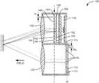
- a one-dimensional optical system 100 for collecting distance information within a fieldincludes: a set of illumination sources 110 arranged along a first axis, each illumination source in the set of illumination sources 110 configured to output an illuminating beam of an operating wavelength toward a discrete spot in the field ahead of the illumination source; a bulk imaging optic 130 characterized by a focal plane opposite the field; an aperture layer 140 coincident the focal plane, defining a set of apertures 144 in a line array parallel to the first axis, and defining a stop region 146 around the set of apertures 144 , each aperture in the set of apertures 144 defining a field of view in the field coincident a discrete spot output by a corresponding illumination source in the set of illumination sources 110 , the stop region 146 absorbing light rays reflected from surfaces in the field outside of fields of view defined by the set of apertures 144 and passing through the bulk imaging optic 130 ; a set of lenses 150 , each lens in the set of lenses 150 , each lens in the set of
- the one-dimensional optical system 100functions as an image sensor that, when rotated about an axis parallel to a column of apertures, collects three-dimensional distance data of a volume occupied by the system.
- the one-dimensional optical system 100can scan a volume to collect three-dimensional distance data that can then be reconstructed into a virtual three-dimensional representation of the volume, such as based on recorded times between transmission of illuminating beams from the illumination sources and detection of photons—likely originating from the illumination sources—incident on the set of pixels 170 , based on phase-based measurements techniques, or based on any other suitable distance measurement technique.
- the system 100includes: a column of offset apertures arranged behind a bulk imaging optic 130 and defining discrete fields of view in a field ahead of the bulk imaging optic 130 (that is non-overlapping fields of view beyond a threshold distance from the system); a set of illumination sources 110 that project discrete illuminating beams at an operating wavelength into (and substantially only into) the fields of view defined by the apertures; a column of lenses that collimate light rays passed by corresponding apertures; and an optical filter 160 that selectively passes a narrow band of wavelengths of light (i.e., electromagnetic radiation) including the operating wavelength; and a set of pixels 170 that detect incident photons (e.g., count incident photons, tracks times between consecutive incident photons).
- incident photonse.g., count incident photons, tracks times between consecutive incident photons.
- the systemcan therefore selectively project illuminating beams into a field ahead of the system according to an illumination pattern that substantially matches—in size and geometry across a range of distances from the system—the fields of view of the apertures.
- the illumination sourcesare configured to illuminate substantially only surfaces in the field ahead of the system that can be detected by pixels in the system such that minimal power output by the system (via the illumination sources) is wasted by illuminating surfaces in the field for which the pixels are blind.
- the systemcan therefore achieve a relatively high ratio of output signal (i.e., illuminating beam power) to input signal (i.e., photons passed to an incident on the pixel array).
- the set of lenses 150can collimate light rays passed by adjacent apertures such that light rays incident on the optical filter 160 meet the optical filter 160 at an angle of incidence of approximately 0°, thereby maintaining a relatively narrow band of wavelengths of light passed by the optical filter 160 and achieving a relatively high signal-to-noise ratio (“SNR”) for light rays reaching the set of pixels 170 .
- SNRsignal-to-noise ratio
- the systemincludes pixels arranged in a column and aligned with the apertures, and each pixel can be non-square in geometry (e.g., short and wide) to extend the sensing area of the system for a fixed aperture pitch and pixel column height.
- the systemalso includes a diffuser 180 that spreads light rays passed from an aperture through the optical filter 160 across the area of a corresponding pixel such that the pixel can detect incident photons across its full width and height thereby increasing the dynamic range of the system.
- the systemis described herein as projecting electromagnetic radiation into a field and detecting electromagnetic radiation reflected from a surface in the field back to bulk receiver optic.
- Terms “illumination beam,” “light,” “light rays,” and “photons” recited hereinrefer to such electromagnetic radiation.
- the term “channel” recited hereinrefers to one aperture in the aperture layer 140 , a corresponding lens in the set of lenses 150 , and a corresponding pixel in the set of pixels 170 .
- the systemincludes a bulk imaging optic 130 characterized by a focal plane opposite the field.
- the bulk imaging optic 130functions to project incident light rays from outside the system toward the focal plane where light rays incident on a stop region 146 of the aperture layer 140 are rejected (e.g., mirrored or absorbed) and where light rays incident on apertures in the aperture layer 140 are passed into a lens characterized by a focal length and offset from the focal plane by the focal length.
- the bulk imaging optic 130includes a converging lens, such as a bi-convex lens (shown in FIG. 2 ) or a plano-convex lens, characterized by a particular focal length at the operating wavelength of the system.
- the bulk imaging optic 130can also include multiple discrete lens that cooperate to project light rays toward the aperture layer 140 and that are characterized by a composite focal plane opposite the field, as shown in FIG. 11 .
- the bulk imaging optic 130can be any other suitable type of lens or combination of lenses of any other type or geometry.
- the systemincludes an aperture layer 140 coincident the focal plane, defining a set of apertures 144 in a line array parallel to the axes of the illumination sources, and defining a stop region 146 around the set of apertures 144 , wherein each aperture in the set of apertures 144 defines a field of view in the field coincident a discrete spot output by a corresponding illumination source in the set of illumination sources 110 , and wherein the stop region 146 absorbs and/or reflects light rays reflected from surfaces in the field outside of fields of view defined by the set of apertures 144 and passing through the bulk imaging optic 130 .
- the aperture layer 140defines an array of open regions (i.e., apertures, including one aperture per lens) and closed regions (“stop regions”) between adjacent opens.
- Each aperture in the aperture layer 140defines a “pinhole” that defines a field of view for its corresponding sense channel and passes light rights reflected from an external surface within its field of the view into its corresponding lens, and each stop region 146 can block light rays incident on select regions of the focal plane from passing into the lens array, as shown in FIG. 6 .
- the aperture layer 140includes a relatively thin opaque structure coinciding with (e.g., arranged along) the focal plane of the bulk imaging optic 130 , as shown in FIGS. 1 and 2 .
- the aperture layer 140can include a 10 micrometer-thick copper, silver, or nickel film deposited (e.g., plated) over a photocurable transparent polymer and then selectively etched to form the array of apertures.
- a reflective metalized layer or a light-absorbing photopolymere.g., a photopolymer mixed with a light absorbing dye
- a photomaskcan be deposited onto a glass wafer and selectively cured with a photomask to form the aperture layer 140 and the set of apertures 144 .
- the aperture layer 140can include a discrete metallic film that is mechanically or chemically perforated to form the array of apertures, bonded to the lens array, and then installed over the bulk imaging optic 130 along the focal plane.
- the aperture layer 140can include any other reflective (e.g., mirrored) or light-absorbing material formed in any other way to define the array of apertures along the focal plane of the bulk imaging optic 130 .
- the aperture layer 140can define a single column of multiple discrete circular apertures of substantially uniform diameter, wherein each aperture defines an axis substantially parallel to and aligned with one lens in the lens array, as shown in FIG. 3 . Adjacent apertures are offset by an aperture pitch distance greater than the aperture diameter and substantially similar to the lens pitch distance, and the aperture layer 140 defines a stop region 146 (i.e., an opaque or reflecting region) between adjacent apertures such that the apertures define discrete, non-overlapping fields of view for their corresponding sense channels.
- a stop region 146i.e., an opaque or reflecting region
- an aperturedefines a narrower field of view (i.e., a field of view of smaller diameter) and passes a sharper but lower-intensity (attenuated) signal from the bulk imaging optic 130 into its corresponding lens.
- the aperture layer 140can therefore define apertures of diameter: greater than the diffraction-limited diameter for the wavelength of light output by the illumination sources (e.g., 900 nm); substantially greater than the thickness of the aperture layer 140 ; and less than the aperture pitch distance, which is substantially equivalent to the lens pitch distance and the pixel pitch distance.
- aperture layer 140can define apertures of diameters approaching the diffraction-limited diameter to maximize geometrical selectivity of the field of view of each sense channel.
- the aperturescan be of diameter less that the diffraction-limited diameter for the wavelength of light output by the illumination sources.
- the aperture layer 140can define apertures of diameters matched to a power output of illumination sources in the system and to a number and photon detection capacity of subpixel photodetectors in each pixel in the set of pixels 170 to achieve a target number of photons incident on each pixel within each sampling period.
- each aperturecan define a particular diameter that achieves target attenuation range for pixels originating from a corresponding illumination source and incident on the bulk imaging optic 130 during a sampling period.
- the diameter of the aperturecan be matched to the dynamic range of its corresponding pixel.
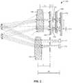
- a first aperture 141 in the aperture layer 140passes light rays—reflected from a discrete region of a surface in the field (the field of view of the sense channel) ahead of the bulk imaging optic 130 —into its corresponding lens; a stop region 146 interposed between the first aperture 141 and adjacent apertures in the aperture layer 140 blocks light rays—reflected from a region of the surface outside of the field of view of the first aperture 141 —from passing into the lens corresponding to the first aperture 141 .
- the aperture layer 140therefore defines a column of apertures that define multiple discrete, non-overlapping fields of view of substantially infinite depth of field, as shown in FIG. 2 .
- a first aperture 141 in the aperture layer 140defines a field of view that is distinct and that does not intersect a field of view defined by another aperture in the aperture layer 140 , as shown in FIG. 2 .
- the set of illumination sources 110includes a first illumination source 111 paired with the first aperture 141 and configured to project an illuminating beam substantially aligned with (i.e., overlapping) the field of view of the first aperture 141 in the field ahead of the bulk imaging optic 130 .
- the first illumination source 111 and a bulk transmitting optic 120can cooperate to project an illuminating beam of a cross-section substantially similar to (and slightly larger than) the cross section of the field of view of the first aperture 141 as various distances from the bulk imaging optic 130 . Therefore light output by the first illumination source 111 —paired with the first aperture 141 —and projected into the field of view of the first aperture 141 can remain substantially outside the fields of view of other apertures in the aperture layer 140 .
- photons projected into the field by the first illumination source 111illuminate a particular region of a surface (or multiple surfaces) in the field within the field of view of the first sense channel and are reflected (e.g., scattered) by the surface(s); at least some of these photons reflected by the particular region of a surface may reach the bulk imaging optic 130 , which directs these photons toward the focal plane.
- the bulk imaging optic 130may project these photons into the first aperture 141 , and the first aperture 141 may pass these photons into the first lens 151 (or a subset of these photons incident at an angle relative to the axis of the first aperture 141 below a threshold angle).
- a second aperture 142 in the aperture layer 140is offset from the first aperture 141 and because the particular region of the surface in the field illuminated via the first illumination source 111 does not (substantially) coincide with the field of view of the second aperture 142 , photons reflected by the particular region of the surface and reaching the bulk imaging optic 130 are projected into the second aperture 142 and passed to a second lens 152 behind the second aperture 142 , and vice versa, as shown in FIG. 2 .
- a stop region 146 between the first and second apertures 142can block photons directed toward the focal plane between the first and second apertures 142 reflected by the bulk imaging optic 130 , thereby reducing crosstalk between the first and second sense channels.
- the first aperture 141 in the aperture layer 140For a first aperture 141 in the aperture layer 140 paired with a first illumination source 111 in the set of illumination sources 110 , the first aperture 141 in the aperture layer 140 defines a first field of view and passes—into the first lens 151 —incident light rays originating at or reflected from a surface in the field coinciding with the first field of view. Because the first illumination source 111 projects an illuminating beam that is substantially coincident (and substantially the same size as or minimally larger than) the field of view defined by the first aperture 141 (as shown in FIG.
- a signal passed into the first lens 151 by the first aperture 141 in the aperture layer 140can exhibit a relatively high ratio of light rays originating from the first illumination source 111 to light rays originating from other illumination sources in the system.
- various illumination sources in the systemmay output illuminating beams at different frequencies, duty cycles, and/or power levels, etc. at a particular time during operation, light rays passed from the bulk imaging optic 130 into a first pixel 171 in the set of pixels 170 but originating from an illumination source other than the first illumination source 111 paired with the first pixel 171 constitute noise at the first pixel 171 .
- each aperture in the aperture layer 140may pass a relatively high proportion of photons originating from its corresponding illumination source than from other illumination sources in the system; that is, due to the geometry of a particular aperture and its corresponding illumination source, a particular aperture may pass a signal exhibiting a relatively high SNR to its corresponding lens and thus into its corresponding pixel.
- the systemcan pass less noise from solar radiation or other ambient light sources to the set of pixels 170 .
- the systemincludes a second aperture layer interposed between the lens array and the optical filter 160 , wherein the second aperture layer defines a second set of apertures 144 , each aligned with a corresponding lens in the set of lenses 150 , as described above.
- an aperture in the second aperture layer 140can absorb or reflect errant light rays passed by a corresponding lens, as described above, to further reduce crosstalk between channels, thereby improving SNR within the system.
- the systemcan additionally or alternatively include a third aperture layer interposed between the optical filter 160 and the diffuser(s) 180 , wherein the third aperture layer defines a third set of apertures 144 , each aligned with a corresponding lens in the set of lenses 150 , as described above.
- an aperture in the third aperture layercan absorb or reflect errant light rays passed by the light filter, as described above, to again reduce crosstalk between channels, thereby improving SNR within the system.
- the systemincludes a set of lenses 150 , wherein each lens in the set of lenses 150 is characterized by a second focal length, is offset from the focal plane opposite the bulk imaging optic 130 by the second focal length, is aligned with a corresponding aperture in the set of apertures 144 , and is configured to collimate light rays passed by the corresponding aperture.
- a lens in the set of lenses 150functions to collimate lights rays passed by its corresponding aperture and to pass these collimated light rays into the optical filter 160 .
- each lenscan include a converging lens characterized by a second focal length and can be offset from the focal plane of the bulk imaging optic 130 —opposite the bulk imaging optic 130 —by the second focal length to preserve the aperture of the bulk imaging optic 130 and to collimate light incident on the bulk imaging optic 130 and passed by a corresponding aperture.
- Each lens in the set of lenscan be characterized by a relatively short focal length (i.e., less than a focal length of the bulk imaging optic 130 ) and a relatively large marginal ray angle (e.g., a relatively high numeric aperture lens) such that the lens can capture highly-angled light rays projected toward the lens by the extent of the bulk imaging optic 130 . That is, each lens in the set of lens can be characterized by a ray cone substantially matched to a ray cone of the bulk imaging optic 130 .
- Lenses in the set of lenses 150can be substantially similar.
- a lens in the set of lenses 150is configured to collimate light rays focused into its corresponding aperture by the bulk imaging optic 130 .
- a lens in the set of lenses 150can include a bi-convex or plano-convex lens characterized by a focal length selected based on the size (e.g., diameter) of its corresponding aperture and the operating wavelength of the system.
- the focal length (f) of a lens in the set of lenses 150can be calculated according to the formula:
- dthe diameter of the corresponding aperture in the aperture layer and ⁇ is the operating wavelength of light output by the illumination source (e.g., 900 nm).
- the geometry of a lens in the set of lenses 150can therefore be matched to the geometry of a corresponding aperture in the aperture layer such that the lens passes a substantially sharp image of light rays—at or near the operating wavelength—into the optical filter 160 and thus on to the pixel array.
- the set of lenses 150can include lenses of any other geometry and arranged in any other way adjacent the aperture layer.
- the systemincludes an optical filter 160 adjacent the set of lenses 150 opposite the aperture layer and configured to pass light rays at the operating wavelength.
- the optical filter 160receives electromagnetic radiation across a spectrum from the set of lenses 150 , passes a relatively narrow band of electromagnetic radiation—including radiation at the operating wavelength—to the pixel array, and blocks electromagnetic radiation outside of the band.
- electromagnetic radiation other than electromagnetic radiation output by the illumination source—such as ambient light—incident on a pixel in the set of pixels 170constitutes noise in the system.
- the optical filter 160therefore functions to reject electromagnetic radiation outside of the operating wavelength or, more pragmatically, outside of a narrow wavelength band, thereby reducing noise in the system and increasing SNR.
- the optical filter 160includes an optical bandpass filter that passes a narrow band of electromagnetic radiation substantially centered at the operating wavelength of the system.
- the illumination sourcesoutput light (predominantly) at an operating wavelength of 900 nm, and the optical filter 160 is configured to pass light between 899.95 nm and 900.05 nm and to block light outside of this band.
- the optical filter 160may selectively pass and reject wavelengths of light as a function of angle of incidence on the optical filter 160 .
- optical bandpass filtersmay pass wavelengths of light inversely proportional to their angle of incidence on the light optical bandpass filter.
- the optical filter 160may pass over 95% of electromagnetic radiation over a sharp band from 899.75 nm to 900.25 nm and reject approximately 100% of electromagnetic radiation below 899.70 nm and above 900.30 nm for light rays incident on the optical filter 160 at an angle of incidence of approximately 0°.
- the optical filter 160may pass over 95% of electromagnetic radiation over a narrow band from 899.5 nm to 900.00 nm and reject approximately 100% of electromagnetic radiation over a much wider band below 899.50 nm and above 900.30 nm for light rays incident on the optical filter 160 at an angle of incidence of approximately 15°. Therefore, the incidence plane of the optical filter 160 can be substantially normal to the axes of the lenses, and the set of lenses 150 can collimate light rays received through a corresponding aperture and output these light rays substantially normal to the incidence plane of the optical filter 160 (i.e., at an angle of incidence of approximately 0° on the optical filter). Specifically, the set of lenses 150 can output light rays toward the optical filter 160 at angles of incidence approximating 0° such that substantially all electromagnetic radiation passed by the optical filter 160 is at or very near the operating wavelength of the system.
- the systemcan include a single optical filter 160 that spans the column of lens in the set of lenses 150 .
- the systemcan include multiple optical filters 160 , each adjacent a single lens or a subset of lenses in the set of lenses 150 .
- the optical filter 160can define any other geometry and can function in any other way to pass only a limited band of wavelengths of light.
- the systemincludes a set of pixels 170 adjacent the optical filter 160 opposite the set of lenses 150 , each pixel in the set of pixels 170 corresponding to a lens in the set of lenses 150 and including a set of subpixels arranged along a second axis non-parallel to the first axis.
- the set of pixels 170are offset from the optical filter 160 opposite the set of lenses 150 , and each pixel in the set of pixels 170 functions to output a single signal or stream of signals corresponding to the count of photons incident on the pixel within one or more sampling periods, wherein each sampling period may be picoseconds, nanoseconds, microseconds, or milliseconds in duration.
- the systemalso includes a diffuser 180 interposed between the optical filter 160 and the set of pixels 170 and configured to spread collimated light output from each lens in the set of lenses 150 across a set of subpixels of a single corresponding pixel in the set of pixels 170 .
- the diffuser 180functions to spread light rays—previously collimated by the lens and passed by the optical filter 160 —across the width and height of a sensing area within a corresponding pixel.
- the diffuser 180can define a single optic element spanning the set of lenses 150 , or the diffuser 180 can include multiple discrete optical elements, such as including one optical diffuser element aligned with each channel in the system.
- a first pixel 171 in the set of pixels 170includes an array of single-photon avalanche diode detectors (hereinafter “SPADs”), and the diffuser 180 spreads lights rays—previously passed by a corresponding first aperture 141 , collimated by a corresponding first lens 151 , and passed by the optical filter 160 —across the area of the first pixel 171 , as shown in FIGS. 3, 5, and 6 .
- SPADssingle-photon avalanche diode detectors
- adjacent aperturescan be aligned and offset vertically by an aperture pitch distance
- adjacent lensescan be aligned and offset vertically by a lens pitch distance substantially identical to the aperture pitch distance
- adjacent pixelscan be aligned and offset vertically by a pixel pitch distance substantially identical to the lens and aperture pitch distances.
- the pixel pitch distancemay accommodate only a relatively small number of (e.g., two) vertically-stacked SPADs.
- Each pixel in the set of pixels 170can therefore define an aspect ratio greater than 1:1, and the diffuser 180 can spread light rays passed by the optical filter 160 according to the geometry of a corresponding pixel in order to accommodate a larger sensing area per pixel.
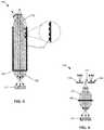
- each pixel in the set of pixels 170is arranged on an image sensor, and a first pixel 171 in the set of pixels 170 includes a single row of 16 SPADs spaced along a lateral axis perpendicular to a vertical axis bisecting the column of apertures and lenses.
- the height of a single SPAD in the first pixel 171can be less than the height (e.g., diameter) of the first lens 151 , but the total length of the 16 SPADs can be greater than the width (e.g., diameter) of the first lens 151 ; the diffuser 180 can therefore converge light rays output from the first lens 151 to a height corresponding to the height of a SPAD at the plane of the first pixel 171 and can diverge light rays output from the first lens 151 to a width corresponding to the width of the 16 SPADs at the plane of the first pixel 171 .
- the remaining pixels in the set of pixels 170can include similar rows of SPADs, and the diffuser 180 can similarly converge and diverge light rays passed by corresponding apertures onto corresponding pixels.
- the aperture layercan include a column of 16 like apertures
- the set of lenses 150can include a column of 16 like lenses arranged behind the aperture layer
- the set of pixels 170can include a set of 16 like pixels—each including a similar array of SPADs—arranged behind the set of lenses 150 .
- each pixelcan include a single row of 16 SPADs, wherein each SPAD is electrically coupled to a remote analog front-end processing electronics/digital processing electronics circuit 240 .
- Each SPADcan be arranged in a 400 ⁇ m-wide, 400 ⁇ m-tall SPAD area and can define an active sensing area approaching 400 ⁇ m in diameter.
- Adjacent SPADscan be offset by a SPAD pitch distance of 400 ⁇ m.
- the aperture pitch distance along the vertical column of apertures, the lens pitch distance along the vertical column of lenses, and the pixel pitch distance along the vertical column of pixelscan each be approximately 400 ⁇ m accordingly.
- a first diffuser 180can diverge a cylindrical column of light rays passed from the first lens 151 through the optical filter 160 —such as a column of light approximately 100 ⁇ m in diameter for an aperture layer aspect ratio of 1:4—to a height of approximately 400 ⁇ m aligned vertically with the row of SPADs in the first pixel 171 .
- the first diffusercan similarly diverge the cylindrical column of light rays passed from the first lens 151 through the optical filter 160 to a width of approximately 6.4 ⁇ m centered horizontally across the row of SPADs in the first pixel 171 .
- diffusers 180 in the systemcan similarly diverge (or converge) collimated light passed by corresponding lenses across corresponding pixels in the set of pixels 170 . Therefore, in this example, by connecting each SPAD (or each pixel) to a remote analog front-end processing electronics/digital processing electronics circuit 240 and by incorporating diffusers 180 that spread light passed by the optical filter 160 across the breadths and heights of corresponding pixels, the system can achieve a relatively high sensing area fill factor across the imaging sensor.
- pixels in the set of pixels 170can include an array of multiple SPADS arranged in aspect ratio exceeding 1:1, and the diffuser 180 can spread light rays across corresponding non-square pixels that enables a relatively large numbers of SPADs to be tiled across a single pixel to achieve a greater dynamic range across the image sensor than an image sensor with a single SPAD per pixel, as shown in FIG. 3 .
- a first sense channel in the systemcan detect multiple incident photons—originating from a surface in the field bound by a field of view defined by the first aperture 141 —within the span of the dead time characteristic of the SPADs.
- the first sense channelcan therefore detect a “brighter” surface in its field of view. Additionally or alternatively, the first pixel 171 in the first sense channel can be sampled faster than the dead time characteristic of SPADs in the first pixel 171 because, though a first subset of SPADs in the first pixel 171 may be down (or “dead”) during a first sampling period due to collection of incident photons during the first sampling period, other SPADs in the first pixel 171 remain on (or “alive”) and can therefore collect incident photons during a subsequent sampling period. Furthermore, by incorporating pixels characterized by relatively high aspect ratios of photodetectors, the image sensor can include pixels offset by a relatively small pixel pitch, but the system 100 can still achieve a relatively high dynamic range pixel.
- pixels in the set of pixels 170can include any other number of SPADs arranged in any other arrays, such as in a 64-by-1 grid array (as described above), in a 32-by-2 grid array, or in a 16-by-4 grid array, and the diffuser 180 can converge and/or diverge collimated light rays onto corresponding pixels accordingly in any other suitable way.
- each pixel in the set of pixels 170can include one or more linear avalanche photodiodes, Geiger mode avalanche photodiodes, photomultipliers, resonant cavity photodiodes, QUANTUM DOT detectors, or other types of photodetectors arranged as described above, and the diffuser(s) 180 can similarly converge and diverge signals passed by the optical filter(s) 160 across corresponding pixels, as described herein.
- the systemincludes a set of illumination sources 110 arranged along a first axis, each illumination source in the set of illumination sources 110 configured to output an illuminating beam of an operating wavelength toward a discrete spot in a field ahead of the illumination source.
- each illumination sourcefunctions to output an illuminating beam coincident a field of view defined by a corresponding aperture in the set of apertures 144 , as shown in FIGS. 1 and 2 .
- the set of illumination sources 110includes a bulk transmitter optic and one discrete emitter per sense channel.
- the set of illumination sources 110can include a monolithic VCSEL arrays including a set of discrete emitters.
- the bulk transmitter opticcan be substantially identical to the bulk imaging optic 130 in material, geometry (e.g., focal length), thermal isolation, etc., and the bulk transmitter optic is adjacent and offset laterally and/or vertically from the bulk imaging optic 130 .
- set of illumination sources 110includes a laser array including discrete emitters arranged in a column with adjacent emitters offset by an emitter pitch distance substantially identical to the aperture pitch distance.
- each emitteroutputs an illuminating beam of diameter substantially identical to or slightly greater than the diameter of a corresponding aperture in the apertures layer
- the column of emittersis arranged along the focal plane of the bulk transmitter optic such that each illuminating beam projected from the bulk transmitter optic into the field intersects and is of substantially the same size and geometry as the field of view of the corresponding sense channel, as shown in FIG. 4 . Therefore, substantially all power output by each emitter in the set of illumination sources 110 can be projected into the field of view of its corresponding sense channel with relatively minimal power wasted illuminating surfaces in the field outside of the fields of view of the sense channels.
- the discrete emittersare similarly arranged in a column with adjacent emitters offset by an emitter pitch distance twice the aperture pitch distance, as shown in FIG. 2 .
- each emitteris characterized by an illuminating active area (or aperture) of diameter approximately (or slightly greater than) twice the diameter of a corresponding aperture in the apertures layer, and the column of emitters is offset behind the bulk transmitter optic by twice the focal length of the bulk transmitter optic such that each illuminating beam projected from the bulk transmitter optic into the field intersects and is of substantially the same size and geometry as the field of view of the corresponding sense channel, as described above.
- an illuminating beam output by an emitter in this second examplemay contain four times the power of an illuminating beam output by an emitter in the first example described above.
- the systemcan therefore include a set of emitter arranged according to an emitter pitch distance, configured to output illuminating beams of diameter, and offset behind the bulk transmitter optic by an offset distance as a function of a scale factor (e.g., 2.0 or 3.0) and 1) the aperture pitch distance in the aperture layer, 2) the diameter of apertures in the aperture layer, and 3) the focal length of bulk transmitter optic, respectively.
- the systemcan therefore include an illuminating subsystem that is proportionally larger than a corresponding receiver subsystem to achieve greater total output illumination power within the same beam angles and fields of view of corresponding channels in the receiver subsystem.
- the systemcan also include multiple discrete sets of illumination sources, each set of illumination sources 110 paired with a discrete bulk transmitter optic adjacent the bulk imaging optic 130 .
- the systemcan include a first bulk transmitter optic, a second bulk transmitter optic, and a third bulk transmitter optic patterned radially about the bulk imaging optic 130 at a uniform radial distance from the center of the bulk imaging optic 130 and spaced apart by an angular distance of 120°.
- the systemcan include a laser array with one emitter—as described above—behind each of the first, second, and third bulk transmitter optics. Each discrete laser array and its corresponding bulk transmitter optic can thus project a set of illuminating beams into the fields of view of defined by corresponding in the apertures in the aperture layer.
- the three discrete laser arrays and the three corresponding bulk transmitter opticscan cooperate to project three times the power onto the fields of view of the sense channels in the system, as compared to a single laser array and one bulk transmitter optic.
- the systemcan include multiple discrete layer arrays and bulk transmitter optics to both: 1) achieve a target illumination power output into the field of view of each sensing channel in the receiver subsystem with multiple lower-power emitters per sensing channel; and 2) distribute optical energy over a larger area in the near-field to achieve an optical energy density less than a threshold allowable optical energy density for the human eye.
- the systemcan include any other number and configuration of illumination source sets and bulk transmitter optics configured to illuminate fields of view defined by the sense channels.
- the set of illumination sources 110can also include any other suitable type of optical transmitter, such as a 1 ⁇ 16 optical splitter powered by a single laser diode, a side-emitting laser diode array, an LED array, or a quantum dot LED array, etc.
- the bulk receiver lens, the aperture layer, the set of lenses 150 , the optical filter 160 , and the diffuser 180are fabricated and then aligned with and mounted onto an image sensor.
- the optical filter 160can be fabricated by coating a fused silica substrate. Photoactive optical polymer can then be deposited over the optical filter 160 , and a lens mold can be placed over the photoactive optical polymer and a UV light source activated to cure the photoactive optical polymer in the form of lenses patterned across the optical filter 160 .
- Standoffscan be similarly molded or formed across the optical filter 160 via photolithography techniques, and an aperture layer defined by a selectively-cured, metallized glass wafer can then be bonded or otherwise mounted to the standoffs to form the aperture layer.
- the assemblycan then be inverted, and a set of discrete diffusers and standoffs can be similarly fabricated across the opposite side of the optical filter 160 .
- a discrete image sensorcan then be aligned with and bonded to the standoffs, and a bulk imaging optic 130 can be similarly mounted over the aperture layer.
- photolithography and wafer level bonding techniquescan be implemented to fabricate the bulk imaging optics, the aperture layer, the set of lenses 150 , the optical filter 160 , and the diffuser 180 directly on to the un-diced semiconductor wafer containing the detector chips in order to simplify manufacturing, reduce cost, and reduce optical stack height for decreased pixel crosstalk.
- One variation of the systemincludes: a set of illumination sources 110 arranged along a first axis, each illumination source in the set of illumination sources 110 configured to output an illuminating beam of an operating wavelength toward a discrete spot in a field ahead of the illumination source; a bulk imaging optic 130 characterized by a focal plane opposite the field; a set of lens tubes 210 arranged in a line array parallel to the first axis, each lens tube in the set of lens tubes 210 including: a lens characterized by a focal length, offset from the focal plane by the focal length, and configured to collimate light rays reflected into the bulk imaging optic 130 from a discrete spot in the field illuminated by a corresponding illumination source in the set of optics into the bulk imaging optic 130 ; and a cylindrical wall 218 extending from the lens opposite the focal plane, defining a long axis substantially perpendicular to the first axis, and configured to absorb incident light rays reflected into the bulk imaging optic 130 from a region in the field outside the discrete spot illuminate
- the systemalso includes: an optical filter 160 adjacent the set of lens tubes 210 opposite the focal plane and configured to pass light rays at the operating wavelength; a set of pixels 170 adjacent the optical filter 160 opposite the set of lenses 150 , each pixel in the set of pixels 170 corresponding to a lens in the set of lenses 150 and including a set of subpixels aligned along a third axis perpendicular to the first axis; and a diffuser 180 interposed between the optical filter 160 and the set of pixels 170 and configured to spread collimated light output from each lens in the set of lenses 150 across a set of subpixels of a corresponding pixel in the set of pixels 170 .
- the systemincludes a lens tube in replacement of (or in addition to) each aperture and lens pair described above.
- each lens tubecan be characterized by a second (short) focal length and can be offset from the focal plane of the bulk imaging optic 130 by the second focal length to preserve the aperture of the bulk imaging optic 130 and to collimate incident light received from the bulk imaging optic 130 , as described above and as shown in FIGS. 5 and 7 .
- Each lens tubealso defines an opaque cylindrical wall 218 defining an axis normal to the incidence plane of the adjacent optical filter 160 and configured to absorb incident light rays, as shown in FIG. 5 .
- the cylindrical wall 218 of a lens tubemay absorb light rays passing through the lens tube at shallower angles to the axis of the lens tube, thereby reducing the field of view of the lens tube (which may be similar to decreasing the diameter of an aperture in the aperture layer up to the diffraction-limited diameter, as described above) and yielding an output signal of collimated light rays nearer to perpendicular to the incidence plane of the optical filter 160 .
- Each lens tubecan therefore define an elongated cylindrical wall 218 of length sufficient to achieve a target field of view and to pass collimated light rays at maximum angles to the axis of the lens tube less than a threshold angle.
- a lens tubecan thus function as an aperture-sense pair described above to define a narrow field of view and to output substantially collimated light to the adjacent optical filter 160 .
- the cylindrical wall 218 of a lens tubecan define a coarse or patterned opaque interface about a transparent (or translucent) lens material, as shown in FIG. 5 , to increase absorption and decrease reflection of light rays incident on the cylindrical wall 218 .
- Each lens tube (and each lens described above)can also be coated with an anti-reflective coating.
- the set of lens tubes 210can be fabricated by implementing photolithography techniques to pattern a photoactive optical polymer (e.g., SU8) onto the optical filter 160 (e.g., on a silicon wafer defining the optical filter).
- a light-absorbing polymercan then be poured between the lens tubes and cured.
- a set of lenses 150can then be fabricated (e.g., molded) separately and then bonded over the lens tubes.
- lensescan be fabricated directly onto the lens tubes by photolithography techniques.
- a mold for lensescan be cast directly onto the lens tubes by injecting polymer into a mold arranged over the lens tubes.
- a singular diffuser 180 or multiple discrete diffusers 180can be similarly fabricated and/or assembled on the optical filter 160 opposite the lens tubes. Standoffs extending from the optical filter 160 can be similarly fabricated or installed around the diffuser(s) 180 , and the image sensor can be aligned with and bonded to the standoffs opposite the optical filter 160 .
- Other optical elements within the systeme.g., the bulk imaging lens, the bulk transmitting lens, etc.
- Another variation of the systemincludes: a set of illumination sources 110 arranged in a first rectilinear grid array, each illumination source in the set of illumination sources 110 configured to output an illuminating beam of an operating wavelength toward a discrete spot in a field ahead of the illumination source; a bulk imaging optic 130 characterized by a focal plane opposite the field; an aperture layer coincident the focal plane, defining a set of apertures 144 in a second rectilinear grid array proportional to the first rectilinear grid array, and defining a stop region 146 around the set of apertures 144 , each aperture in the set of apertures 144 defining a field of view in the field coincident a discrete spot output by a corresponding illumination source in the set of illumination sources 110 , the stop region 146 absorbing light rays reflected from surfaces in the field outside of fields of view defined by the set of apertures 144 and passing through the bulk imaging optic 130 ; a set of lenses 150 , each lens in the set of lenses 150 characterized by
- the systemincludes a two-dimensional grid array of channels (i.e., aperture, lens, and pixel sets or lens tube and pixel sets) and is configured to image a volume occupied by the system in two dimensions.
- the systemcan collect one-dimensional distance data—such as counts of incident photons within a sampling period and/or times between consecutive photons incident on pixels of known position corresponding to known fields of view in the field—across a two-dimensional field.
- the one-dimensional distance datacan then be merged with known positions of the fields of view for each channel in the system to reconstruct a virtual three-dimensional representation of the field ahead of the system.
- the aperture layercan define a grid array of apertures
- the set of lenses 150can be arranged in a similar grid array with one lens aligned with one aperture in the aperture layer
- the set of pixels 170can include one pixel per aperture and lens pair, as described above.
- the aperture layercan define a 24-by-24 grid array of 200- ⁇ m-diameter apertures offset vertically and laterally by an aperture pitch distance of 300 ⁇ m
- the set of lenses 150can similarly define a 24-by-24 grid array of lenses offset vertically and laterally by a lens pitch distance of 300 ⁇ m
- the set of pixels 170can include a 24-by-24 grid array of 300- ⁇ m-square pixels, wherein each pixel includes a 3 ⁇ 3 square array of nine 100- ⁇ m-square SPADs.
- the set of pixels 170can include one pixel per group of multiple aperture and lens pairs.
- the set of pixels 170can alternatively include a 12-by-12 grid array of 600- ⁇ m-square pixels, wherein each pixel includes a 6 ⁇ 6 square array of 36 100- ⁇ m-square SPADs and wherein each pixel is aligned with a group of four adjacent lenses in a square grid.
- the diffuser 180can bias collimated light rays output from a lens in the (1,1) position in the square grid upward and to the right to spread light rays passing through the (1,1) lens across the full breadth and width of the corresponding pixel; can bias collimated light rays output from a lens in the (2,1) position in the square grid upward and to the left to spread light rays passing through the (2,1) lens across the full breadth and width of the corresponding pixel; can bias collimated light rays output from a lens in the (1,2) position in the square grid downward and to the right to spread light rays passing through the (1,2) lens across the full breadth and width of the corresponding pixel; and can bias collimated light rays output from a lens in the (2,2) position in the square grid downward and to the left to spread light rays passing through the (2,2) lens across the full breadth and width of the corresponding pixel, as shown in FIG. 8 .
- the systemcan actuate one illumination source in the group of four illumination sources at any given instance in time.
- the systemcan actuate a first illumination source 111 in a (1,1) position during a first sampling period to illuminate a field of view defined by a first aperture 141 corresponding to a lens in the (1,1) position in the corresponding group of four lenses, and the system can sample all 36 SPADs in the corresponding pixel during the first sampling period.
- the systemcan then shut down the first illumination source 111 and actuate a second illumination source 112 in a (1,2) position during a subsequent second sampling period to illuminate a field of view defined by a second aperture 142 corresponding to a lens in the (1,2) position in the corresponding group of four lenses, and the system can sample all 36 SPADs in the corresponding pixel during the second sampling period.
- the systemcan then shut down the first and second illumination sources 112 and actuate a third illumination source in a (2,1) position during a subsequent third sampling period to illuminate a field of view defined by a third aperture corresponding to a lens in the (2,1) position in the corresponding group of four lenses, and the system can sample all 36 SPADs in the corresponding pixel during the third sampling period.
- the systemcan shut down the first, second, and third illumination sources and actuate a fourth illumination source in a (2,2) position during a fourth sampling period to illuminate a field of view defined by a fourth aperture corresponding to a lens in the (2,2) position in the corresponding group of four lenses, and the system can sample all 36 SPADs in the corresponding pixel during the fourth sampling period.
- the systemcan repeat this process throughout its operation.
- the systemcan include a set of pixels 170 arranged across an image sensor 7.2 mm in width and 7.2 mm in length and can implement a scanning schema such that each channel in the system can access (can project light rays onto) a number of SPADs otherwise necessitating a substantially larger image sensor (e.g., a 14.4 mm by 14.4 mm image sensor).
- the systemcan implement a serial scanning schema per group of illumination sources to achieve an exponential increase in the dynamic range of each channel in the system.
- the systemcan implement the foregoing imaging techniques to increase imaging resolution of the system.
- the systemcan also include a shutter 182 between each channel and the image sensor, and the system can selectively open and close each shutter 182 when the illumination source for the corresponding channel is actuated and deactivated, respectively.
- the systemcan include one independently-operable electrochromic shutter 182 interposed between each lens, and the system can open the electrochromic shutter 182 over the (1,1) lens in the square-gridded group of four lenses and close electrochromic shutters 182 over the (1,2), (2,1), and (2,2) lens when the (1,1) illumination source is activated, thereby rejecting noise passing through the (1,2), (2,1), and (2,2) lens from reaching the corresponding pixel on the image sensor.
- the systemcan therefore selectively open and close shutters 182 between each channel and the image sensor to increase SNR per channel during operation.
- the systemcan include one independently-operable electrochromic shutter 182 arranged over select regions of each pixel, as shown in FIG. 8 , wherein each electrochromic shutter 182 is aligned with a single channel (i.e., with a single lens in the set of lenses).
- the systemcan alternatively include MEMS mechanical shutters or any other suitable type of shutter interposed between the set of lenses 150 and the image sensor.
- the systemcan define two-dimension grid arrays of apertures, lenses, diffusers, and/or pixels characterized by a first pitch distance along a first (e.g., X) axis and a second pitch distance—different from the first pitch distance—along a second (e.g., Y) axis.
- the image sensorcan include pixels offset by a 25 ⁇ m horizontal pitch and a 300 ⁇ m vertical pitch, wherein each pixel includes a single row of twelve subpixels.
- the two-dimensional optical systemcan include an array of any other number and pattern of channels (e.g., apertures, lenses (or lens tubes), and diffusers) and pixels and can execute any other suitable scanning schema to achieve higher spatial resolutions per channel than the raw pixel resolution of the image sensor.
- the systemcan additionally or alternatively include a converging optic, a diverging optic, and/or any other suitable type of optical element to spread light rights passed from a channel across the breadth of a corresponding pixel.
Landscapes
- Physics & Mathematics (AREA)
- General Physics & Mathematics (AREA)
- Optics & Photonics (AREA)
- Engineering & Computer Science (AREA)
- Computer Networks & Wireless Communication (AREA)
- Radar, Positioning & Navigation (AREA)
- Remote Sensing (AREA)
- Spectroscopy & Molecular Physics (AREA)
- Health & Medical Sciences (AREA)
- Toxicology (AREA)
- Signal Processing (AREA)
- Multimedia (AREA)
- Electromagnetism (AREA)
- Measurement Of Optical Distance (AREA)
- Investigating Or Analysing Materials By Optical Means (AREA)
- Lenses (AREA)
- Optical Radar Systems And Details Thereof (AREA)
- Automatic Focus Adjustment (AREA)
- Studio Devices (AREA)
- Semiconductor Lasers (AREA)
- Photo Coupler, Interrupter, Optical-To-Optical Conversion Devices (AREA)
- Length Measuring Devices By Optical Means (AREA)
- Transforming Light Signals Into Electric Signals (AREA)
- Optical Elements Other Than Lenses (AREA)
- Light Receiving Elements (AREA)
- Solid State Image Pick-Up Elements (AREA)
- Photometry And Measurement Of Optical Pulse Characteristics (AREA)
Abstract
Description
where d is the diameter of the corresponding aperture in the aperture layer and λ is the operating wavelength of light output by the illumination source (e.g., 900 nm). The geometry of a lens in the set of
Claims (20)
Priority Applications (4)
| Application Number | Priority Date | Filing Date | Title |
|---|---|---|---|
| US16/584,515US11202056B2 (en) | 2015-09-24 | 2019-09-26 | Optical system with multiple light emitters sharing a field of view of a pixel detector |
| US17/549,675US11627298B2 (en) | 2015-09-24 | 2021-12-13 | Optical system for collecting distance information within a field |
| US18/179,559US11956410B2 (en) | 2015-09-24 | 2023-03-07 | Optical system for collecting distance information within a field |
| US18/613,587US12200183B2 (en) | 2015-09-24 | 2024-03-22 | Optical system for collecting distance information within a field |
Applications Claiming Priority (5)
| Application Number | Priority Date | Filing Date | Title |
|---|---|---|---|
| US201562232222P | 2015-09-24 | 2015-09-24 | |
| US15/276,532US9992477B2 (en) | 2015-09-24 | 2016-09-26 | Optical system for collecting distance information within a field |
| US15/880,491US11025885B2 (en) | 2015-09-24 | 2018-01-25 | Optical system for collecting distance information within a field |
| US16/046,643US11190750B2 (en) | 2015-09-24 | 2018-07-26 | Optical imaging system with a plurality of sense channels |
| US16/584,515US11202056B2 (en) | 2015-09-24 | 2019-09-26 | Optical system with multiple light emitters sharing a field of view of a pixel detector |
Related Parent Applications (1)
| Application Number | Title | Priority Date | Filing Date |
|---|---|---|---|
| US16/046,643ContinuationUS11190750B2 (en) | 2015-09-24 | 2018-07-26 | Optical imaging system with a plurality of sense channels |
Related Child Applications (1)
| Application Number | Title | Priority Date | Filing Date |
|---|---|---|---|
| US17/549,675ContinuationUS11627298B2 (en) | 2015-09-24 | 2021-12-13 | Optical system for collecting distance information within a field |
Publications (2)
| Publication Number | Publication Date |
|---|---|
| US20200036959A1 US20200036959A1 (en) | 2020-01-30 |
| US11202056B2true US11202056B2 (en) | 2021-12-14 |
Family
ID=59960008
Family Applications (9)
| Application Number | Title | Priority Date | Filing Date |
|---|---|---|---|
| US15/276,532Active2036-10-15US9992477B2 (en) | 2015-09-24 | 2016-09-26 | Optical system for collecting distance information within a field |
| US15/880,491Active2038-09-01US11025885B2 (en) | 2015-09-24 | 2018-01-25 | Optical system for collecting distance information within a field |
| US16/046,643Active2038-02-25US11190750B2 (en) | 2015-09-24 | 2018-07-26 | Optical imaging system with a plurality of sense channels |
| US16/584,515ActiveUS11202056B2 (en) | 2015-09-24 | 2019-09-26 | Optical system with multiple light emitters sharing a field of view of a pixel detector |
| US17/317,809ActiveUS11196979B2 (en) | 2015-09-24 | 2021-05-11 | Optical system for collecting distance information within a field |
| US17/323,962ActiveUS11178381B2 (en) | 2015-09-24 | 2021-05-18 | Optical system for collecting distance information within a field |
| US17/549,675ActiveUS11627298B2 (en) | 2015-09-24 | 2021-12-13 | Optical system for collecting distance information within a field |
| US18/179,559ActiveUS11956410B2 (en) | 2015-09-24 | 2023-03-07 | Optical system for collecting distance information within a field |
| US18/613,587ActiveUS12200183B2 (en) | 2015-09-24 | 2024-03-22 | Optical system for collecting distance information within a field |
Family Applications Before (3)
| Application Number | Title | Priority Date | Filing Date |
|---|---|---|---|
| US15/276,532Active2036-10-15US9992477B2 (en) | 2015-09-24 | 2016-09-26 | Optical system for collecting distance information within a field |
| US15/880,491Active2038-09-01US11025885B2 (en) | 2015-09-24 | 2018-01-25 | Optical system for collecting distance information within a field |
| US16/046,643Active2038-02-25US11190750B2 (en) | 2015-09-24 | 2018-07-26 | Optical imaging system with a plurality of sense channels |
Family Applications After (5)
| Application Number | Title | Priority Date | Filing Date |
|---|---|---|---|
| US17/317,809ActiveUS11196979B2 (en) | 2015-09-24 | 2021-05-11 | Optical system for collecting distance information within a field |
| US17/323,962ActiveUS11178381B2 (en) | 2015-09-24 | 2021-05-18 | Optical system for collecting distance information within a field |
| US17/549,675ActiveUS11627298B2 (en) | 2015-09-24 | 2021-12-13 | Optical system for collecting distance information within a field |
| US18/179,559ActiveUS11956410B2 (en) | 2015-09-24 | 2023-03-07 | Optical system for collecting distance information within a field |
| US18/613,587ActiveUS12200183B2 (en) | 2015-09-24 | 2024-03-22 | Optical system for collecting distance information within a field |
Country Status (11)
| Country | Link |
|---|---|
| US (9) | US9992477B2 (en) |
| JP (1) | JP7214629B2 (en) |
| KR (2) | KR102309478B1 (en) |
| CN (2) | CN109983312B (en) |
| CA (1) | CA3038038A1 (en) |
| DE (2) | DE112017004806T5 (en) |
| DK (1) | DK180852B1 (en) |
| GB (2) | GB2601435B (en) |
| IL (1) | IL265562B2 (en) |
| SE (1) | SE544865C2 (en) |
| WO (1) | WO2018057084A1 (en) |
Cited By (3)
| Publication number | Priority date | Publication date | Assignee | Title |
|---|---|---|---|---|
| US20210041570A1 (en)* | 2017-05-15 | 2021-02-11 | Ouster, Inc. | Augmenting panoramic lidar results with color |
| US11422236B2 (en) | 2016-08-24 | 2022-08-23 | Ouster, Inc. | Optical system for collecting distance information within a field |
| US11627298B2 (en) | 2015-09-24 | 2023-04-11 | Ouster, Inc. | Optical system for collecting distance information within a field |
Families Citing this family (124)
| Publication number | Priority date | Publication date | Assignee | Title |
|---|---|---|---|---|
| US11609336B1 (en) | 2018-08-21 | 2023-03-21 | Innovusion, Inc. | Refraction compensation for use in LiDAR systems |
| GB201511551D0 (en) | 2015-07-01 | 2015-08-12 | St Microelectronics Res & Dev | Photonics device |
| US10063849B2 (en) | 2015-09-24 | 2018-08-28 | Ouster, Inc. | Optical system for collecting distance information within a field |
| EP3408677A4 (en) | 2016-01-29 | 2019-10-09 | Ouster, Inc. | SYSTEMS AND METHODS FOR CALIBRATING AN OPTICAL DISTANCE SENSOR |
| US10761195B2 (en) | 2016-04-22 | 2020-09-01 | OPSYS Tech Ltd. | Multi-wavelength LIDAR system |
| JP2019523422A (en)* | 2016-08-04 | 2019-08-22 | オフィール オプトロニクス ソリューションズ リミテッド | Photometric test system for light emitting devices |
| US11275155B1 (en)* | 2016-11-08 | 2022-03-15 | Lockheed Martin Coherent Technologies, Inc. | Laser-array lidar devices |
| US10605984B2 (en) | 2016-12-01 | 2020-03-31 | Waymo Llc | Array of waveguide diffusers for light detection using an aperture |
| US10502618B2 (en) | 2016-12-03 | 2019-12-10 | Waymo Llc | Waveguide diffuser for light detection using an aperture |
| WO2018182812A2 (en) | 2016-12-30 | 2018-10-04 | Innovusion Ireland Limited | Multiwavelength lidar design |
| US10942257B2 (en) | 2016-12-31 | 2021-03-09 | Innovusion Ireland Limited | 2D scanning high precision LiDAR using combination of rotating concave mirror and beam steering devices |
| US11009605B2 (en) | 2017-01-05 | 2021-05-18 | Innovusion Ireland Limited | MEMS beam steering and fisheye receiving lens for LiDAR system |
| US11054508B2 (en) | 2017-01-05 | 2021-07-06 | Innovusion Ireland Limited | High resolution LiDAR using high frequency pulse firing |
| US10969475B2 (en) | 2017-01-05 | 2021-04-06 | Innovusion Ireland Limited | Method and system for encoding and decoding LiDAR |
| US10571679B2 (en)* | 2017-01-06 | 2020-02-25 | Karl Storz Imaging, Inc. | Endoscope incorporating multiple image sensors for increased resolution |
| DE102017101945A1 (en)* | 2017-02-01 | 2018-08-02 | Osram Opto Semiconductors Gmbh | Measuring arrangement with an optical transmitter and an optical receiver |
| KR102619582B1 (en) | 2017-03-13 | 2024-01-02 | 옵시스 테크 엘티디 | Eye-Safe Scanning LIDAR System |
| EP3639057B1 (en)* | 2017-05-11 | 2021-11-03 | Huawei Technologies Co., Ltd. | Time-of-flight apparatus |
| DE202018006696U1 (en) | 2017-05-15 | 2022-04-01 | Ouster, Inc. | Optical image transmitter with brightness improvement |
| CN113466882A (en) | 2017-07-05 | 2021-10-01 | 奥斯特公司 | Optical distance measuring device |
| KR102218679B1 (en) | 2017-07-28 | 2021-02-23 | 옵시스 테크 엘티디 | VCSEL Array LIDAR Transmitter with Small Angle Divergence |
| US10791283B2 (en)* | 2017-09-01 | 2020-09-29 | Facebook Technologies, Llc | Imaging device based on lens assembly with embedded filter |
| US10785400B2 (en) | 2017-10-09 | 2020-09-22 | Stmicroelectronics (Research & Development) Limited | Multiple fields of view time of flight sensor |
| CN111542765B (en) | 2017-10-19 | 2024-08-02 | 图达通智能美国有限公司 | LIDAR with large dynamic range |
| EP3710855A4 (en) | 2017-11-15 | 2021-08-04 | Opsys Tech Ltd. | Noise adaptive solid-state lidar system |
| JP2019101244A (en)* | 2017-12-04 | 2019-06-24 | 富士通株式会社 | Optical module |
| JP7120756B2 (en)* | 2017-12-05 | 2022-08-17 | シャープ株式会社 | Photodetector, time-of-flight measuring device and optical radar device |
| US11353556B2 (en) | 2017-12-07 | 2022-06-07 | Ouster, Inc. | Light ranging device with a multi-element bulk lens system |
| US11493601B2 (en) | 2017-12-22 | 2022-11-08 | Innovusion, Inc. | High density LIDAR scanning |
| US11977184B2 (en) | 2018-01-09 | 2024-05-07 | Seyond, Inc. | LiDAR detection systems and methods that use multi-plane mirrors |
| US11675050B2 (en) | 2018-01-09 | 2023-06-13 | Innovusion, Inc. | LiDAR detection systems and methods |
| US11391823B2 (en) | 2018-02-21 | 2022-07-19 | Innovusion, Inc. | LiDAR detection systems and methods with high repetition rate to observe far objects |
| WO2019164961A1 (en) | 2018-02-21 | 2019-08-29 | Innovusion Ireland Limited | Lidar systems with fiber optic coupling |
| WO2019165289A1 (en) | 2018-02-22 | 2019-08-29 | Innovusion Ireland Limited | Receive path for lidar system |
| US11808888B2 (en) | 2018-02-23 | 2023-11-07 | Innovusion, Inc. | Multi-wavelength pulse steering in LiDAR systems |
| US12085673B2 (en) | 2018-02-23 | 2024-09-10 | Seyond, Inc. | Distributed LiDAR systems |
| WO2019165294A1 (en) | 2018-02-23 | 2019-08-29 | Innovusion Ireland Limited | 2-dimensional steering system for lidar systems |
| WO2019245614A2 (en) | 2018-03-09 | 2019-12-26 | Innovusion Ireland Limited | Lidar safety systems and methods |
| KR102604050B1 (en) | 2018-04-01 | 2023-11-22 | 옵시스 테크 엘티디 | Noise adaptive solid-state lidar system |
| US11789132B2 (en) | 2018-04-09 | 2023-10-17 | Innovusion, Inc. | Compensation circuitry for lidar receiver systems and method of use thereof |
| WO2019199775A1 (en) | 2018-04-09 | 2019-10-17 | Innovusion Ireland Limited | Lidar systems and methods for exercising precise control of a fiber laser |
| DE102018109544A1 (en)* | 2018-04-20 | 2019-10-24 | Sick Ag | Optoelectronic sensor and method for distance determination |
| CN112585492B (en) | 2018-06-15 | 2024-10-25 | 图达通智能美国有限公司 | LIDAR system and method for focusing a range of interest |
| DE102018118653B4 (en) | 2018-08-01 | 2020-07-30 | Sick Ag | Optoelectronic sensor and method for detecting an object |
| JP2021532368A (en) | 2018-08-03 | 2021-11-25 | オプシス テック リミテッド | Distributed modular solid-state lidar system |
| US10739189B2 (en)* | 2018-08-09 | 2020-08-11 | Ouster, Inc. | Multispectral ranging/imaging sensor arrays and systems |
| US10760957B2 (en) | 2018-08-09 | 2020-09-01 | Ouster, Inc. | Bulk optics for a scanning array |
| US11579300B1 (en) | 2018-08-21 | 2023-02-14 | Innovusion, Inc. | Dual lens receive path for LiDAR system |
| US11860316B1 (en) | 2018-08-21 | 2024-01-02 | Innovusion, Inc. | Systems and method for debris and water obfuscation compensation for use in LiDAR systems |
| US11614526B1 (en) | 2018-08-24 | 2023-03-28 | Innovusion, Inc. | Virtual windows for LIDAR safety systems and methods |
| US11796645B1 (en) | 2018-08-24 | 2023-10-24 | Innovusion, Inc. | Systems and methods for tuning filters for use in lidar systems |
| US11579258B1 (en) | 2018-08-30 | 2023-02-14 | Innovusion, Inc. | Solid state pulse steering in lidar systems |
| WO2020057125A1 (en)* | 2018-09-18 | 2020-03-26 | Shenzhen GOODIX Technology Co., Ltd. | Depth information construction system, associated electronic device, and method for constructing depth information |
| US12313788B1 (en) | 2018-10-09 | 2025-05-27 | Seyond, Inc. | Ultrashort pulses in LiDAR systems |
| WO2020102406A1 (en) | 2018-11-14 | 2020-05-22 | Innovusion Ireland Limited | Lidar systems and methods that use a multi-facet mirror |
| US10852434B1 (en)* | 2018-12-11 | 2020-12-01 | Facebook Technologies, Llc | Depth camera assembly using fringe interferometery via multiple wavelengths |
| US11947038B2 (en) | 2018-12-21 | 2024-04-02 | Continental Automotive Systems, Inc. | Wavelength adaptive narrow band optical filter for a LIDAR system |
| US11585906B2 (en) | 2018-12-26 | 2023-02-21 | Ouster, Inc. | Solid-state electronic scanning laser array with high-side and low-side switches for increased channels |
| US11675055B2 (en) | 2019-01-10 | 2023-06-13 | Innovusion, Inc. | LiDAR systems and methods with beam steering and wide angle signal detection |
| US11486970B1 (en) | 2019-02-11 | 2022-11-01 | Innovusion, Inc. | Multiple beam generation from a single source beam for use with a LiDAR system |
| EP3699640B1 (en) | 2019-02-19 | 2022-01-26 | Sick Ag | Optoelectronic sensor and method for detecting an object |
| JP7527760B2 (en)* | 2019-03-18 | 2024-08-05 | キヤノン株式会社 | Lens device and imaging device |
| JP2020153796A (en) | 2019-03-19 | 2020-09-24 | 株式会社リコー | Distance measuring device and distance measuring method |
| US11977185B1 (en) | 2019-04-04 | 2024-05-07 | Seyond, Inc. | Variable angle polygon for use with a LiDAR system |
| CN113692540B (en) | 2019-04-09 | 2025-06-17 | 欧普赛斯技术有限公司 | Solid-state LIDAR transmitter with laser control |
| CN120762041A (en) | 2019-04-26 | 2025-10-10 | 上海禾赛科技有限公司 | Laser radar and its detection device |
| US12153133B2 (en) | 2019-04-26 | 2024-11-26 | Ouster, Inc. | Independent per-pixel integration registers for LIDAR measurements |
| EP3948344A4 (en)* | 2019-05-01 | 2022-12-21 | Sense Photonics, Inc. | Event driven shared memory pixel |
| KR102856043B1 (en) | 2019-05-13 | 2025-09-08 | 아우스터, 인크. | Synchronized Image Capture for Electronic Scanning LIDAR Systems |
| US11555891B2 (en) | 2019-05-21 | 2023-01-17 | Northrop Grumman Systems Corporation | Methods for large angle field of view scanning LIDAR with no movable parts |
| US11531111B2 (en) | 2019-05-21 | 2022-12-20 | Northrop Grumman Systems Corporation | 360 degrees field of view scanning lidar with no movable parts |
| US11448732B2 (en) | 2019-05-21 | 2022-09-20 | Northrop Grumman Systems Corporation | Frequency modulated scanning LIDAR with 360 degrees field of view |
| JP7603998B2 (en) | 2019-05-30 | 2024-12-23 | オプシス テック リミテッド | Eye-safe long-range LIDAR system using actuators |
| US11513195B2 (en) | 2019-06-10 | 2022-11-29 | OPSYS Tech Ltd. | Eye-safe long-range solid-state LIDAR system |
| EP3990943A4 (en) | 2019-06-25 | 2023-07-05 | Opsys Tech Ltd. | Adaptive multiple-pulse lidar system |
| US10861819B1 (en)* | 2019-07-05 | 2020-12-08 | Asm Technology Singapore Pte Ltd | High-precision bond head positioning method and apparatus |
| US10701326B1 (en)* | 2019-07-10 | 2020-06-30 | Lightspace Technologies, SIA | Image display system, method of operating image display system and image projecting device |
| KR20220038691A (en) | 2019-07-31 | 2022-03-29 | 옵시스 테크 엘티디 | High-Resolution Solid-State LIDAR Transmitter |
| KR20210020469A (en) | 2019-08-14 | 2021-02-24 | 삼성전자주식회사 | Spectral camera |
| DE102019126982A1 (en) | 2019-10-08 | 2021-04-08 | Sick Ag | Optoelectronic sensor and method for detecting objects |
| KR102684228B1 (en) | 2019-10-21 | 2024-07-11 | 삼성전자주식회사 | Multi-input folded camera and mobile device including the same |
| DE102019129986A1 (en) | 2019-11-07 | 2021-05-12 | Sick Ag | Optoelectronic sensor and method for detecting objects |
| CN115097463A (en)* | 2019-12-20 | 2022-09-23 | 深圳市速腾聚创科技有限公司 | Receiver, Transceiver and Lidar |
| EP4081885B1 (en)* | 2019-12-26 | 2025-09-03 | ams International AG | A sensing system |
| DE102020102247A1 (en) | 2020-01-30 | 2021-08-05 | Sick Ag | Optoelectronic sensor and method for detecting objects |
| CN113472995B (en)* | 2020-03-31 | 2022-12-06 | 深圳市安思疆科技有限公司 | Dynamic automatic focusing system and method based on SPAD sensor receiving module |
| US11695911B2 (en) | 2020-04-27 | 2023-07-04 | Ouster, Inc. | Stereoscopic image capturing systems |
| US11876109B2 (en)* | 2020-05-06 | 2024-01-16 | Semiconductor Components Industries, Llc | Semiconductor devices with single-photon avalanche diodes and light spreading lenses |
| JP7554064B2 (en)* | 2020-06-30 | 2024-09-19 | 株式会社ヴィーネックス | Foreign body/defect inspection device, image generating device for foreign body/defect inspection, and foreign body/defect inspection method |
| DE102020209849A1 (en) | 2020-08-05 | 2022-02-10 | Robert Bosch Gesellschaft mit beschränkter Haftung | Method for determining an optical crosstalk of a lidar sensor and lidar sensor |
| US11579265B2 (en) | 2020-08-19 | 2023-02-14 | Continental Autonomous Mobility US, LLC | Lidar system with crosstalk reduction comprising a power supply circuit layer stacked between an avalanche-type diode layer and a read-out circuit layer |
| US11977169B2 (en) | 2020-08-24 | 2024-05-07 | Innoviz Technologies Ltd. | Multi-beam laser emitter with common optical path |
| US20220170783A1 (en)* | 2020-09-18 | 2022-06-02 | MicroAdventure Technologies LLC | Lensless imager for laser detection |
| EP4001866A1 (en)* | 2020-11-20 | 2022-05-25 | STMicroelectronics S.r.l. | Radiation sensor with an integrated mechanical optical modulator and related manufacturing process |
| TWI805152B (en)* | 2020-12-26 | 2023-06-11 | 以色列商趣眼有限公司 | Method, electrooptical system, and non-transitory computer-readable medium for image generation |
| US20240050608A1 (en)* | 2021-01-04 | 2024-02-15 | Signify Holding B.V. | A disinfection system comprising an optical arrangement for a far uv light source to filter out undesired wavelengths |
| CN116746144A (en)* | 2021-01-15 | 2023-09-12 | Lg伊诺特有限公司 | camera module |
| US12061289B2 (en) | 2021-02-16 | 2024-08-13 | Innovusion, Inc. | Attaching a glass mirror to a rotating metal motor frame |
| US11422267B1 (en) | 2021-02-18 | 2022-08-23 | Innovusion, Inc. | Dual shaft axial flux motor for optical scanners |
| CN114994640A (en)* | 2021-03-01 | 2022-09-02 | 中强光电股份有限公司 | Optical sensing system |
| US11789128B2 (en) | 2021-03-01 | 2023-10-17 | Innovusion, Inc. | Fiber-based transmitter and receiver channels of light detection and ranging systems |
| CN112965243B (en)* | 2021-03-10 | 2022-10-04 | 北京航空航天大学 | Compact eye pattern (sclera blood vessel) imaging device |
| US11657523B2 (en)* | 2021-03-17 | 2023-05-23 | The Trustees Of Princeton University | Microlens amplitude masks for flying pixel removal in time-of-flight imaging |
| CN115236636A (en)* | 2021-04-16 | 2022-10-25 | 上海禾赛科技有限公司 | Receiver and Lidar |
| US20220333911A1 (en)* | 2021-04-20 | 2022-10-20 | Egis Technology Inc. | Distance sensing apparatus |
| US11555895B2 (en) | 2021-04-20 | 2023-01-17 | Innovusion, Inc. | Dynamic compensation to polygon and motor tolerance using galvo control profile |
| US11614521B2 (en) | 2021-04-21 | 2023-03-28 | Innovusion, Inc. | LiDAR scanner with pivot prism and mirror |
| WO2022225859A1 (en) | 2021-04-22 | 2022-10-27 | Innovusion, Inc. | A compact lidar design with high resolution and ultra-wide field of view |
| CN117178199A (en) | 2021-04-22 | 2023-12-05 | 图达通智能美国有限公司 | Compact light detection and ranging design with high resolution and ultra wide field of view |
| CN113156557B (en)* | 2021-04-30 | 2023-02-21 | 浙江光珀智能科技有限公司 | Optical mask and optical system |
| EP4314885A1 (en) | 2021-05-12 | 2024-02-07 | Innovusion, Inc. | Systems and apparatuses for mitigating lidar noise, vibration, and harshness |
| EP4314884A1 (en) | 2021-05-21 | 2024-02-07 | Innovusion, Inc. | Movement profiles for smart scanning using galvonometer mirror inside lidar scanner |
| US11768294B2 (en) | 2021-07-09 | 2023-09-26 | Innovusion, Inc. | Compact lidar systems for vehicle contour fitting |
| IT202100020006A1 (en)* | 2021-07-27 | 2023-01-27 | St Microelectronics Srl | LASER SCANNING APPARATUS AND PROCEDURE |
| US20240345225A1 (en)* | 2021-08-09 | 2024-10-17 | Wemems Co., Ltd. | Scanning mirror-based lidar device |
| DE102021124430B3 (en) | 2021-09-21 | 2022-11-03 | Sick Ag | Visualize lidar measurement data |
| CN216356147U (en) | 2021-11-24 | 2022-04-19 | 图达通智能科技(苏州)有限公司 | Vehicle-mounted laser radar motor, vehicle-mounted laser radar and vehicle |
| EP4460338B1 (en) | 2022-01-04 | 2025-07-16 | Signify Holding B.V. | A radiation generating system comprising an optical arrangement for a far uv light source minimizing the impact of unfiltered undesired wavelengths |
| EP4469827A1 (en)* | 2022-01-30 | 2024-12-04 | Ouster, Inc. | Overlapping sub-ranges with power stepping |
| US11871130B2 (en) | 2022-03-25 | 2024-01-09 | Innovusion, Inc. | Compact perception device |
| US12204033B2 (en) | 2022-03-25 | 2025-01-21 | Seyond, Inc. | Multimodal detection with integrated sensors |
| US20230316554A1 (en)* | 2022-03-30 | 2023-10-05 | Analog Devices, Inc. | Miniaturized phase calibration apparatus for time-of-flight depth camera |
| US20230375679A1 (en)* | 2022-05-17 | 2023-11-23 | Stmicroelectronics (Research & Development) Limited | Quantum film direct time of flight sensor circuit for low cost short wave infrared operation |
| CN115966865B (en)* | 2022-12-29 | 2024-06-14 | 中国电子科技集团公司第二十六研究所 | MEMS filter capable of generating out-of-band zero based on three-dimensional stacking and manufacturing method thereof |
Citations (235)
| Publication number | Priority date | Publication date | Assignee | Title |
|---|---|---|---|---|
| US4358851A (en) | 1980-02-28 | 1982-11-09 | Xerox Corporation | Fiber optic laser device and light emitter utilizing the device |
| EP0095725A1 (en) | 1982-05-31 | 1983-12-07 | Kabushiki Kaisha Toshiba | Area sensor |
| US4634272A (en) | 1982-06-02 | 1987-01-06 | Nissan Motor Company, Limited | Optical radar system with an array of photoelectric sensors |
| US4676599A (en) | 1985-08-14 | 1987-06-30 | The United States Of America As Represented By The Secretary Of The Air Force | Micro-optical lens holder |
| US4702600A (en) | 1984-07-20 | 1987-10-27 | Litef Gmbh | Method and apparatus for measuring angular rate with a passive optical resonator |
| US4744667A (en) | 1986-02-11 | 1988-05-17 | University Of Massachusetts | Microspectrofluorimeter |
| US4851664A (en) | 1988-06-27 | 1989-07-25 | United States Of America As Represented By The Secretary Of The Navy | Narrow band and wide angle hemispherical interference optical filter |
| JPH036407A (en) | 1989-06-03 | 1991-01-11 | Daido Steel Co Ltd | Outer circumferential shape measuring device |
| US5188286A (en) | 1991-12-18 | 1993-02-23 | International Business Machines Corporation | Thermoelectric piezoelectric temperature control |
| US5267016A (en) | 1991-11-27 | 1993-11-30 | United Technologies Corporation | Laser diode distance measurement |
| US5268748A (en) | 1991-02-13 | 1993-12-07 | U.S. Philips Corporation | Arrangement for measuring the reflection and/or transmission of an object |
| US5288992A (en) | 1992-12-15 | 1994-02-22 | Gte Laboratories Incorporated | Wide angle, narrow band optical filter |
| JPH0749417A (en) | 1993-08-06 | 1995-02-21 | Fujitsu Ltd | Interference filter assembly |
| JPH07181023A (en) | 1993-09-30 | 1995-07-18 | Komatsu Ltd | Cofocal optical system |
| JPH07318325A (en) | 1994-05-26 | 1995-12-08 | Matsushita Electric Works Ltd | Method and apparatus for detection of shape |
| US5659420A (en) | 1993-09-30 | 1997-08-19 | Kabushiki Kaisha Komatsu Seisakusho | Confocal optical apparatus |
| JPH09257440A (en) | 1996-03-26 | 1997-10-03 | Takaoka Electric Mfg Co Ltd | Two-dimensional array type confocal optical device |
| JPH10311950A (en) | 1997-05-14 | 1998-11-24 | Olympus Optical Co Ltd | Scanning microscope |
| US5953110A (en) | 1998-04-23 | 1999-09-14 | H.N. Burns Engineering Corporation | Multichannel laser radar |
| US5982552A (en) | 1994-12-29 | 1999-11-09 | Nippon Sheet Glass Co., Ltd | Planar microlens array having high converging efficiency |
| US6014232A (en) | 1996-09-07 | 2000-01-11 | U.S. Philips Corporation | Electrical device comprising an array of pixels |
| US6043873A (en) | 1997-01-10 | 2000-03-28 | Advanced Optical Technologies, Llc | Position tracking system |
| US6104516A (en) | 1996-06-11 | 2000-08-15 | Canon Kabushiki Kaisha | Wavelength-changeable light source capable of changing wavelength of output light, optical communication network using the same and wavelength control method for controlling wavelength |
| US6133989A (en) | 1993-02-09 | 2000-10-17 | Advanced Scientific Concepts, Inc. | 3D imaging laser radar |
| US6255133B1 (en) | 1998-11-19 | 2001-07-03 | Xerox Corporation | Electro optical devices with reduced filter thinning on the edge pixel photosites and method of producing same |
| US20020003617A1 (en) | 1999-03-18 | 2002-01-10 | Guenter Doemens | Spatially resolving range-finding system |
| US6374024B1 (en) | 1998-10-30 | 2002-04-16 | Sharp Kabushiki Kaisha | Image sensor and method of manufacturing the same |
| US6414746B1 (en) | 1999-11-24 | 2002-07-02 | Advanced Scientific Concepts, Inc. | 3-D imaging multiple target laser radar |
| US20030006676A1 (en) | 2001-05-29 | 2003-01-09 | Smith Stuart T. | Closed loop control systems employing relaxor ferroelectric actuators |
| US20030047752A1 (en) | 2000-09-29 | 2003-03-13 | Campbell Joe C. | Avalanche photodiodes with an impact-ionization-engineered multiplication region |
| US6690019B2 (en) | 1997-09-16 | 2004-02-10 | Advanced Scientific Concepts, Inc. | High data rate smart sensor |
| US20040061502A1 (en) | 1999-09-14 | 2004-04-01 | Hasser Christopher J. | High-resolution optical encoder with phased-array photodetectors |
| US6721262B1 (en) | 1997-09-22 | 2004-04-13 | Seagate Technology Llc | Aperture stop for a flying optical head |
| JP2004247461A (en) | 2003-02-13 | 2004-09-02 | Toyota Central Res & Dev Lab Inc | Monitoring device and monitoring method |
| US20040223071A1 (en) | 2003-05-08 | 2004-11-11 | David Wells | Multiple microlens system for image sensors or display units |
| US20050030409A1 (en) | 2003-08-08 | 2005-02-10 | Matherson Kevin J. | Method and apparatus for generating data representative of an image |
| US20050046850A1 (en) | 2003-07-11 | 2005-03-03 | Svt Associates, Inc. | Film mapping system |
| US7091462B2 (en) | 2002-08-26 | 2006-08-15 | Jds Uniphase Corporation | Transmitter with laser monitoring and wavelength stabilization circuit |
| US20060244851A1 (en) | 2005-05-02 | 2006-11-02 | Andrew Cartlidge | Increasing fill-factor on pixelated sensors |
| USD531525S1 (en) | 2004-11-02 | 2006-11-07 | Sick Ag | Optoelectronic sensor |
| US20070007563A1 (en) | 2004-06-01 | 2007-01-11 | Chandra Mouli | Silicon-based resonant cavity photodiode for image sensors |
| US7170542B2 (en) | 2003-01-23 | 2007-01-30 | Orbotech Ltd. | System and method for providing high brightness illumination |
| US20070057211A1 (en) | 2005-05-25 | 2007-03-15 | Karsten Bahlman | Multifocal imaging systems and method |
| US20070060806A1 (en) | 2005-04-27 | 2007-03-15 | Martin Hunter | Raman spectroscopy for non-invasive glucose measurements |
| JP2007103590A (en) | 2005-10-03 | 2007-04-19 | Nikon Corp | Imaging device, focus detection apparatus, and imaging system |
| US20070228262A1 (en) | 2005-12-19 | 2007-10-04 | Daniel Cantin | Object-detecting lighting system and method |
| US7295298B2 (en) | 2001-06-05 | 2007-11-13 | Ibeo Automobile Sensor Gmbh | Detection method and a detection apparatus |
| KR20070112679A (en) | 2006-05-22 | 2007-11-27 | 삼성에스디아이 주식회사 | Laser irradiation apparatus and manufacturing method of organic light emitting device using same |
| US20080037114A1 (en) | 2006-05-05 | 2008-02-14 | Visitech International Ltd. | Laser confocal scanning microscope and methods of improving image quality in such microscope |
| US7345271B2 (en) | 2002-09-25 | 2008-03-18 | Ibeo Automobile Sensor Gmbh | Optoelectric sensing device with common deflection device |
| US20080153189A1 (en) | 2003-09-30 | 2008-06-26 | Osram Opto Semiconductors Gmbh | Method for producing a radiation-emitting-and-receiving semiconductor chip |
| US7421159B2 (en) | 2005-12-13 | 2008-09-02 | Board of Supervisor of Louisiana State University and Agricultural and Mechanical College | Integral pre-aligned micro-optical systems |
| US20080218612A1 (en) | 2007-03-09 | 2008-09-11 | Border John N | Camera using multiple lenses and image sensors in a rangefinder configuration to provide a range map |
| US7433042B1 (en) | 2003-12-05 | 2008-10-07 | Surface Optics Corporation | Spatially corrected full-cubed hyperspectral imager |
| US20090016642A1 (en) | 2000-07-14 | 2009-01-15 | Massachusetts Institute Of Technology | Method and system for high resolution, ultra fast 3-d imaging |
| US20090040629A1 (en) | 2006-03-24 | 2009-02-12 | Bechtel Jon H | Vision System |
| US20090179142A1 (en) | 2006-01-23 | 2009-07-16 | Jacques Duparre | Image Detection System and Method For Production at Least One Image Detection System |
| US20090236505A1 (en) | 2005-09-19 | 2009-09-24 | Nereo Pallaro | Multifunctional optical sensor comprising a photodetectors matrix coupled to a microlenses matrix |
| CN101563595A (en) | 2006-12-12 | 2009-10-21 | 皇家飞利浦电子股份有限公司 | Sample concentration detector with temperature compensation |
| EP2124069A1 (en) | 2008-03-20 | 2009-11-25 | IBEO Automobile Sensor GmbH | Omnidirectional lidar system |
| US20090295910A1 (en) | 2005-03-24 | 2009-12-03 | Jose Mir | Hyperspectral Imaging System and Methods Thereof |
| US20100008588A1 (en) | 2008-07-08 | 2010-01-14 | Chiaro Technologies LLC | Multiple channel locating |
| US20100020306A1 (en) | 2006-07-13 | 2010-01-28 | Velodyne Acoustics, Inc. | High definition lidar system |
| US20100110275A1 (en) | 2007-04-06 | 2010-05-06 | Gilles Mathieu | Large depth-of-field imaging system and iris recogniton system |
| US20100123893A1 (en) | 2008-11-17 | 2010-05-20 | Dezhong Yang | Laser distance measuring device |
| JP2010128122A (en) | 2008-11-27 | 2010-06-10 | Olympus Corp | Imaging apparatus |
| US20100204964A1 (en) | 2009-02-09 | 2010-08-12 | Utah State University | Lidar-assisted multi-image matching for 3-d model and sensor pose refinement |
| US20100250700A1 (en) | 2009-03-30 | 2010-09-30 | Sun Microsystems, Inc. | Data storage system and method of processing a data access request |
| US7808706B2 (en) | 2004-02-12 | 2010-10-05 | Tredegar Newco, Inc. | Light management films for displays |
| US7873601B1 (en) | 2006-06-29 | 2011-01-18 | Emc Corporation | Backup of incremental metadata in block based backup systems |
| US7876456B2 (en) | 2009-05-11 | 2011-01-25 | Mitutoyo Corporation | Intensity compensation for interchangeable chromatic point sensor components |
| US20110022566A1 (en) | 2009-06-26 | 2011-01-27 | Simplivt Corporation | File system |
| US20110025843A1 (en) | 2009-07-31 | 2011-02-03 | Mesa Imaging Ag | Time of Flight Camera with Rectangular Field of Illumination |
| US20110032398A1 (en) | 2009-08-06 | 2011-02-10 | Victor Lenchenkov | Image sensor with multilayer interference filters |
| US20110037849A1 (en) | 2008-04-11 | 2011-02-17 | Cristiano Niclass | Time-of-flight based imaging system using a display as illumination source |
| US20110116262A1 (en) | 2009-11-13 | 2011-05-19 | Phoseon Technology, Inc. | Economical partially collimating reflective micro optical array |
| WO2011063347A2 (en) | 2009-11-20 | 2011-05-26 | Pelican Imaging Corporation | Capturing and processing of images using monolithic camera array with heterogeneous imagers |
| US8013983B2 (en) | 2007-12-28 | 2011-09-06 | Industrial Technology Research Institute | Three-dimensional surround scanning device and method thereof |
| US20110216304A1 (en) | 2006-07-13 | 2011-09-08 | Velodyne Acoustics, Inc. | High definition lidar system |
| US20110228142A1 (en) | 2009-10-14 | 2011-09-22 | Fraunhofer-Gesellschaft Zur Foerderung Der Angewandten Forschung E.V. | Device, image processing device and method for optical imaging |
| US20110283113A1 (en) | 2010-05-14 | 2011-11-17 | Oracle International Corporation | Method and system for encrypting data |
| US20110320865A1 (en) | 2010-06-25 | 2011-12-29 | International Business Machines Corporation | Deduplication in a hybrid storage environment |
| US20120044476A1 (en) | 2008-05-09 | 2012-02-23 | Ball Aerospace & Technologies Corp. | Systems and methods of scene and action capture using imaging system incorporating 3d lidar |
| US8130367B2 (en) | 2005-12-08 | 2012-03-06 | Roger Stettner | Laser ranging, tracking and designation using 3-D focal planes |
| WO2012055966A1 (en) | 2010-10-27 | 2012-05-03 | MAX-PLANCK-Gesellschaft zur Förderung der Wissenschaften e.V. | Protecting data integrity with storage leases |
| USD659030S1 (en) | 2010-07-30 | 2012-05-08 | Sick Ag | Optoelectronic sensor |
| US20120140109A1 (en) | 2010-12-06 | 2012-06-07 | Primesense Ltd. | Lens Arrays for Pattern Projection and Imaging |
| US20120141104A1 (en) | 2010-12-03 | 2012-06-07 | Research In Motion Limited | Dynamic lighting control in hybrid camera - projector device |
| US20120154914A1 (en) | 2010-12-16 | 2012-06-21 | Denso Corporation | Interference filter assembly |
| US20120182464A1 (en) | 2011-01-18 | 2012-07-19 | Primesense Ltd. | Objective optics with interference filter |
| JP2012202776A (en) | 2011-03-24 | 2012-10-22 | Toyota Central R&D Labs Inc | Distance measuring device |
| US20120287417A1 (en) | 2011-05-11 | 2012-11-15 | Yvan Mimeault | Multiple-field-of-view scannerless optical rangefinder in high ambient background light |
| US8319949B2 (en) | 2007-06-18 | 2012-11-27 | Leddartech Inc. | Method for detecting objects with visible light |
| JP2012530917A (en) | 2009-06-22 | 2012-12-06 | トヨタ モーター ヨーロッパ ナームロゼ フェンノートシャップ/ソシエテ アノニム | Optical distance meter using pulsed light |
| KR20120137432A (en) | 2010-04-05 | 2012-12-20 | 퀄컴 인코포레이티드 | Combining data from multiple image sensors |
| US20120320164A1 (en) | 2011-06-16 | 2012-12-20 | Lenny Lipton | Stereoscopic camera with polarizing apertures |
| US8374405B2 (en) | 2009-08-28 | 2013-02-12 | Hon Hai Precision Industry Co., Ltd. | Camera device and identity recognition method utilizing the same |
| US20130038941A1 (en) | 2011-08-09 | 2013-02-14 | Primesense Ltd. | Lens Array Projector |
| US20130044310A1 (en) | 2007-12-21 | 2013-02-21 | Leddartech Inc. | Distance detection method and system |
| US20130044187A1 (en) | 2011-08-18 | 2013-02-21 | Sick Ag | 3d camera and method of monitoring a spatial zone |
| US8384997B2 (en) | 2008-01-21 | 2013-02-26 | Primesense Ltd | Optical pattern projection |
| KR20130038388A (en) | 2010-07-19 | 2013-04-17 | 프라운호퍼-게젤샤프트 츄어 푀르더룽 데어 안게반텐 포르슝에.파우. | Image recording device and method for recording an image |
| US20130110779A1 (en) | 2010-05-03 | 2013-05-02 | Panzura, Inc. | Archiving data for a distributed filesystem |
| US20130111262A1 (en) | 2010-05-03 | 2013-05-02 | Panzura, Inc. | Providing disaster recovery for a distributed filesystem |
| US20130141549A1 (en) | 2010-06-29 | 2013-06-06 | Cyclomedia Technology B.V. | Method for Producing a Digital Photo Wherein at Least Some of the Pixels Comprise Position Information, and Such a Digital Photo |
| EP2615566A2 (en) | 2012-01-13 | 2013-07-17 | Nexenta Systems, Inc. | Unified local storage supporting file and cloud object access |
| US8494252B2 (en) | 2007-06-19 | 2013-07-23 | Primesense Ltd. | Depth mapping using optical elements having non-uniform focal characteristics |
| US8504529B1 (en) | 2009-06-19 | 2013-08-06 | Netapp, Inc. | System and method for restoring data to a storage device based on a backup image |
| CN103234527A (en) | 2013-04-07 | 2013-08-07 | 南京理工大学 | Multispectral Light Field Camera |
| US20130206967A1 (en) | 2012-02-15 | 2013-08-15 | Primesense Ltd. | Integrated optoelectronic modules |
| US20130229646A1 (en) | 2012-03-02 | 2013-09-05 | Seiko Epson Corporation | Component analyzer |
| US20130294089A1 (en) | 2007-04-02 | 2013-11-07 | Primesense Ltd. | Pattern projection using micro-lenses |
| US20130300840A1 (en) | 2010-12-23 | 2013-11-14 | Fastree 3D S.A. | 3d landscape real-time imager and corresponding imaging methods |
| US20140006354A1 (en) | 2010-05-03 | 2014-01-02 | Panzura, Inc. | Executing a cloud command for a distributed filesystem |
| US8645810B2 (en) | 2011-07-31 | 2014-02-04 | Sandisk Technologies Inc. | Fast detection of convergence or divergence in iterative decoding |
| US8675181B2 (en) | 2009-06-02 | 2014-03-18 | Velodyne Acoustics, Inc. | Color LiDAR scanner |
| US20140118493A1 (en) | 2009-04-16 | 2014-05-01 | Primesense Ltd. | Three-dimensional mapping and imaging |
| US20140118335A1 (en) | 2012-10-30 | 2014-05-01 | Primesense Ltd. | Depth mapping with enhanced resolution |
| US8742325B1 (en) | 2013-07-31 | 2014-06-03 | Google Inc. | Photodetector array on curved substrate |
| US8743176B2 (en) | 2009-05-20 | 2014-06-03 | Advanced Scientific Concepts, Inc. | 3-dimensional hybrid camera and production system |
| US20140153001A1 (en) | 2012-03-22 | 2014-06-05 | Primesense Ltd. | Gimbaled scanning mirror array |
| US20140158900A1 (en) | 2012-12-11 | 2014-06-12 | Samsung Electronics Co., Ltd. | Photon-counting detector and readout circuit |
| US20140168631A1 (en) | 2012-12-18 | 2014-06-19 | Pouch Holdings LLC | Multi-clad Fiber Based Optical Apparatus and Methods for Light Detection and Ranging Sensors |
| US8762798B2 (en) | 2011-11-16 | 2014-06-24 | Stec, Inc. | Dynamic LDPC code rate solution |
| US20140211194A1 (en) | 2013-01-27 | 2014-07-31 | Quanergy Systems, Inc. | Cost-effective lidar sensor for multi-signal detection, weak signal detection and signal disambiguation and method of using same |
| US8829406B2 (en) | 2009-11-15 | 2014-09-09 | Primesense Ltd. | Optical projector with beam monitor including sensing intensity of beam pattern not projected toward an object |
| US8836922B1 (en) | 2013-08-20 | 2014-09-16 | Google Inc. | Devices and methods for a rotating LIDAR platform with a shared transmit/receive path |
| US20140269796A1 (en) | 2012-01-31 | 2014-09-18 | Flir Systems, Inc. | Multi-wavelength vcsel array to reduce speckle |
| US20140267878A1 (en) | 2011-11-04 | 2014-09-18 | Imec | Spectral camera with overlapping segments of image copies interleaved onto sensor array |
| US20140285628A1 (en) | 2010-02-23 | 2014-09-25 | Primesense Ltd. | Wideband ambient light rejection |
| WO2014150856A1 (en) | 2013-03-15 | 2014-09-25 | Pelican Imaging Corporation | Array camera implementing quantum dot color filters |
| US8848039B2 (en) | 2008-07-09 | 2014-09-30 | Primesense Ltd. | Integrated processor for 3D mapping |
| US20140291491A1 (en) | 2012-03-22 | 2014-10-02 | Primesense Ltd. | Calibration of time-of-flight measurement using stray reflections |
| US20140313519A1 (en) | 2013-03-15 | 2014-10-23 | Primesense Ltd. | Depth scanning with multiple emitters |
| US20140375977A1 (en) | 2013-06-21 | 2014-12-25 | David Ludwig | LIDAR Device and Method for Clear and Degraded Environmental Viewing Conditions |
| US20140376092A1 (en) | 2013-06-19 | 2014-12-25 | Primesense Ltd. | Integrated structured-light projector |
| US20150002636A1 (en) | 2013-06-28 | 2015-01-01 | Cable Television Laboratories, Inc. | Capturing Full Motion Live Events Using Spatially Distributed Depth Sensing Cameras |
| WO2015037211A1 (en) | 2013-09-11 | 2015-03-19 | Sony Corporation | Image processing device and method |
| WO2015052616A1 (en) | 2013-10-09 | 2015-04-16 | Koninklijke Philips N.V. | Monolithic led arrays for uniform and high-brightness light sources |
| US20150115131A1 (en) | 2013-10-28 | 2015-04-30 | Omnivision Technologies, Inc. | Stacked chip spad image sensor |
| US20150124094A1 (en) | 2013-11-05 | 2015-05-07 | Delphi Technologies, Inc. | Multiple imager vehicle optical sensor system |
| US20150131080A1 (en) | 2013-11-12 | 2015-05-14 | Facet Technology Corp. | Methods and Apparatus for Array Based Lidar Systems with Reduced Interference |
| US9063549B1 (en) | 2013-03-06 | 2015-06-23 | Google Inc. | Light detection and ranging device with oscillating mirror driven by magnetically interactive coil |
| KR20150072439A (en) | 2012-10-19 | 2015-06-29 | 퀄컴 인코포레이티드 | Multi-camera system using folded optics |
| US9071763B1 (en) | 2012-09-26 | 2015-06-30 | Google Inc. | Uniform illumination image capture |
| US20150186287A1 (en) | 2013-12-30 | 2015-07-02 | Michael Henry Kass | Using Memory System Programming Interfacing |
| US20150184999A1 (en) | 2005-05-10 | 2015-07-02 | Advanced Scientific Concepts Inc. | Dimensioning system |
| US20150192677A1 (en) | 2014-01-03 | 2015-07-09 | Quanergy Systems, Inc. | Distributed lidar sensing system for wide field of view three dimensional mapping and method of using same |
| US9086273B1 (en) | 2013-03-08 | 2015-07-21 | Google Inc. | Microrod compression of laser beam in combination with transmit lens |
| JP2015137987A (en) | 2014-01-24 | 2015-07-30 | アズビル株式会社 | Distance sensor and distance measuring method |
| US9111444B2 (en) | 2012-10-31 | 2015-08-18 | Raytheon Company | Video and lidar target detection and tracking system and method for segmenting moving targets |
| EP2908166A2 (en) | 2014-02-17 | 2015-08-19 | Yokogawa Electric Corporation | Confocal optical scanner |
| US20150260830A1 (en) | 2013-07-12 | 2015-09-17 | Princeton Optronics Inc. | 2-D Planar VCSEL Source for 3-D Imaging |
| WO2015136100A2 (en) | 2014-03-14 | 2015-09-17 | Mesa Imaging Ag | Optoelectronic modules operable to recognize spurious reflections and to compensate for errors caused by spurious reflections |
| US20150293224A1 (en) | 2013-05-09 | 2015-10-15 | Quanergy Systems, Inc. | Solid state optical phased array lidar and method of using same |
| US20150292948A1 (en) | 2013-08-02 | 2015-10-15 | Verifood, Ltd. | Spectrometry system with diffuser |
| US9164511B1 (en) | 2013-04-17 | 2015-10-20 | Google Inc. | Use of detected objects for image processing |
| WO2015163074A1 (en) | 2014-04-22 | 2015-10-29 | シャープ株式会社 | Optical sensor system, optical-type gas sensor system, microparticle sensor system, light-emitting device, and image printing device |
| US9176051B2 (en) | 2011-06-29 | 2015-11-03 | Karlsruher Institut Fuer Technologie | Micro-optical element, micro-optical array, and optical sensor system |
| US20150316473A1 (en) | 2014-05-01 | 2015-11-05 | Rebellion Photonics, Inc. | Mobile gas and chemical imaging camera |
| US20150319349A1 (en) | 2012-11-21 | 2015-11-05 | Nokia Technologies Oy | A Module for Plenoptic Camera System |
| US20150355470A1 (en) | 2012-12-31 | 2015-12-10 | Iee International Electronics & Engineering S.A. | Optical system generating a structured light field from an array of light sources by means of a refracting or reflecting light structuring element |
| US20150358601A1 (en) | 2009-12-23 | 2015-12-10 | Mesa Imaging Ag | Optical Filter on Objective Lens for 3D Cameras |
| US20150362585A1 (en) | 2013-07-12 | 2015-12-17 | Princeton Optronics Inc. | 2-D Planar VCSEL Source for 3-D Imaging |
| US20150379371A1 (en) | 2014-06-30 | 2015-12-31 | Microsoft Corporation | Object Detection Utilizing Geometric Information Fused With Image Data |
| US20150378241A1 (en) | 2014-06-30 | 2015-12-31 | Quanergy Systems, Inc. | Planar beam forming and steering optical phased array chip and method of using same |
| US9229109B2 (en) | 2011-09-15 | 2016-01-05 | Advanced Scientific Concepts, Inc. | Automatic range corrected flash ladar camera |
| US20160003946A1 (en) | 2014-07-03 | 2016-01-07 | Advanced Scientific Concepts, Inc. | Ladar sensor for a dense environment |
| US20160047897A1 (en) | 2014-08-15 | 2016-02-18 | US LADAR, Inc. | Method and System for Ladar Transmission with Interline Skipping for Dynamic Scan Patterns |
| US20160049765A1 (en) | 2014-08-15 | 2016-02-18 | Quanergy Systems, Inc. | Three-dimensional-mapping two-dimensional-scanning lidar based on one-dimensional-steering optical phased arrays and method of using same |
| US20160047901A1 (en) | 2012-12-25 | 2016-02-18 | Quanergy Systems, Inc. | Robust lidar sensor for broad weather, shock and vibration conditions |
| US9281841B2 (en) | 2012-10-31 | 2016-03-08 | Avago Technologies General Ip (Singapore) Pte. Ltd. | Load balanced decoding of low-density parity-check codes |
| US9285477B1 (en) | 2013-01-25 | 2016-03-15 | Apple Inc. | 3D depth point cloud from timing flight of 2D scanned light beam pulses |
| US9299731B1 (en) | 2013-09-30 | 2016-03-29 | Google Inc. | Systems and methods for selectable photodiode circuits |
| EP3002548A1 (en) | 2014-10-02 | 2016-04-06 | Sick Ag | Illumination device and method for generating an illumination field |
| US20160097858A1 (en) | 2014-10-06 | 2016-04-07 | The Boeing Company | Backfilling clouds of 3d coordinates |
| US9330464B1 (en) | 2014-12-12 | 2016-05-03 | Microsoft Technology Licensing, Llc | Depth camera feedback |
| US20160150963A1 (en) | 2011-09-26 | 2016-06-02 | Michael Lee Roukes | One-photon integrated neurophotonic systems |
| US20160161600A1 (en) | 2013-08-19 | 2016-06-09 | Quanergy Systems, Inc. | Optical phased array lidar system and method of using same |
| US9369689B1 (en) | 2015-02-24 | 2016-06-14 | HypeVR | Lidar stereo fusion live action 3D model video reconstruction for six degrees of freedom 360° volumetric virtual reality video |
| US9368936B1 (en) | 2013-09-30 | 2016-06-14 | Google Inc. | Laser diode firing system |
| US9383753B1 (en) | 2012-09-26 | 2016-07-05 | Google Inc. | Wide-view LIDAR with areas of special attention |
| EP3045935A1 (en) | 2015-01-13 | 2016-07-20 | XenomatiX BVBA | Surround sensing system with dome-filter assembly |
| WO2016116733A1 (en) | 2015-01-20 | 2016-07-28 | Milan Momcilo Popovich | Holographic waveguide lidar |
| US20160218727A1 (en) | 2014-10-31 | 2016-07-28 | Seiko Epson Corporation | Quantum interference device, atomic oscillator, electronic apparatus, and moving object |
| WO2016125165A2 (en) | 2015-02-05 | 2016-08-11 | Verifood, Ltd. | Spectrometry system with visible aiming beam |
| US9425654B2 (en) | 2013-09-30 | 2016-08-23 | Google Inc. | Contactless electrical coupling for a rotatable LIDAR device |
| US9435891B2 (en) | 2012-02-15 | 2016-09-06 | Heptagon Micro Optics Pte. Ltd. | Time of flight camera with stripe illumination |
| US20160265902A1 (en) | 2015-03-12 | 2016-09-15 | Apple Inc. | Thin psd for laser-scanning systems |
| US20160291134A1 (en) | 2015-04-06 | 2016-10-06 | Google Inc. | Long Range Steerable LIDAR System |
| US9470520B2 (en) | 2013-03-14 | 2016-10-18 | Apparate International C.V. | LiDAR scanner |
| US20160306032A1 (en) | 2013-11-22 | 2016-10-20 | Brent S. SCHWARZ | Lidar scanner calibration |
| US9489601B2 (en) | 2012-09-05 | 2016-11-08 | X Development Llc | Construction zone sign detection |
| US20160327779A1 (en) | 2014-01-17 | 2016-11-10 | The Trustees Of Columbia University In The City Of New York | Systems And Methods for Three Dimensional Imaging |
| US20160328619A1 (en) | 2013-12-24 | 2016-11-10 | Lg Electronics Inc. | Vehicle driving assistance device and vehicle having the same |
| US9525863B2 (en) | 2015-04-29 | 2016-12-20 | Apple Inc. | Time-of-flight depth mapping with flexible scan pattern |
| US9529079B1 (en) | 2015-03-26 | 2016-12-27 | Google Inc. | Multiplexed multichannel photodetector |
| US9551791B2 (en) | 2013-07-09 | 2017-01-24 | Xenomatix Nv | Surround sensing system |
| US20170146640A1 (en) | 2015-11-25 | 2017-05-25 | Velodyne Lidar, Inc. | Three Dimensional LIDAR System With Targeted Field of View |
| US20170219695A1 (en) | 2016-01-31 | 2017-08-03 | Velodyne Lidar, Inc. | Multiple Pulse, LIDAR Based 3-D Imaging |
| WO2017132704A1 (en) | 2016-01-31 | 2017-08-03 | Velodyne Lidar, Inc. | Lidar based 3-d imaging with far-field illumination overlap |
| US20170219426A1 (en) | 2016-01-29 | 2017-08-03 | Ouster, Inc. | Systems and Methods for Calibrating an Optical Distance Sensor |
| US20170269215A1 (en) | 2016-03-19 | 2017-09-21 | Velodyne Lidar, Inc. | Integrated Illumination And Detection For LIDAR Based 3-D Imaging |
| US20170269198A1 (en) | 2016-03-21 | 2017-09-21 | Velodyne Lidar, Inc. | LIDAR Based 3-D Imaging With Varying Illumination Field Density |
| US20170269197A1 (en) | 2016-03-21 | 2017-09-21 | Velodyne Lidar, Inc. | LIDAR Based 3-D Imaging With Varying Illumination Intensity |
| US20170269209A1 (en) | 2016-03-21 | 2017-09-21 | Velodyne Lidar, Inc. | LIDAR Based 3-D Imaging With Varying Pulse Repetition |
| US20170289524A1 (en) | 2015-09-24 | 2017-10-05 | Ouster, Inc. | Optical System for Collecting Distance Information Within a Field |
| US20170299700A1 (en) | 2014-10-20 | 2017-10-19 | Quanergy Systems, Inc. | Three-dimensional lidar sensor based on two-dimensional scanning of one-dimensional optical emitter and method of using same |
| US20170303829A1 (en) | 2014-08-21 | 2017-10-26 | I.r Med Ltd. | System and method for noninvasive analysis of subcutaneous tissue |
| US20170350983A1 (en) | 2016-06-01 | 2017-12-07 | Velodyne Lidar, Inc. | Multiple Pixel Scanning LIDAR |
| US9866241B2 (en) | 2015-09-25 | 2018-01-09 | SK Hynix Inc. | Techniques for adaptive LDPC decoding |
| US20180032396A1 (en) | 2016-07-29 | 2018-02-01 | Sandisk Technologies Llc | Generalized syndrome weights |
| US20180038959A1 (en) | 2013-12-06 | 2018-02-08 | Kazuhiro Akatsu | Object detector and sensor |
| US20180059222A1 (en) | 2016-08-24 | 2018-03-01 | Ouster, Inc. | Optical system for collecting distance information within a field |
| WO2018065428A2 (en) | 2016-10-03 | 2018-04-12 | Xenomatix Nv | System for determining a distance to an object |
| WO2018065427A1 (en) | 2016-10-03 | 2018-04-12 | Xenomatix Nv | System for determining a distance to an object |
| WO2018065429A1 (en) | 2016-10-03 | 2018-04-12 | Xenomatix Nv | System and method for determining a distance to an object |
| WO2018065426A1 (en) | 2016-10-03 | 2018-04-12 | Xenomatix Nv | Method for subtracting background light from an exposure value of a pixel in an imaging array, and pixel for use in same |
| EP3316000A1 (en) | 2016-10-28 | 2018-05-02 | Xenomatix NV | Vehicular system for measuring a distance to an object and method of installing same |
| US20180167602A1 (en) | 2015-09-24 | 2018-06-14 | Ouster, Inc. | Optical system for collecting distance information within a field |
| WO2018122415A1 (en) | 2016-12-30 | 2018-07-05 | Xenomatix Nv | System for characterizing surroundings of a vehicle |
| US20180299554A1 (en) | 2015-10-23 | 2018-10-18 | Xenomatix Nv | System and method for determining a distance to an object |
| WO2018197441A1 (en) | 2017-04-23 | 2018-11-01 | Xenomatix Nv | A pixel structure |
| US20180329065A1 (en) | 2017-05-15 | 2018-11-15 | Ouster, Inc. | Optical imaging transmitter with brightness enhancement |
| US10183541B2 (en) | 2015-01-13 | 2019-01-22 | Xenomatix Nv | Surround sensing system with telecentric optics |
| US20190097653A1 (en) | 2017-09-22 | 2019-03-28 | SK Hynix Memory Solutions America Inc. | Memory system with decoders and method of operating such memory system and decoders |
| US20190103885A1 (en) | 2017-09-29 | 2019-04-04 | Nyquist Semiconductor Limited | Systems and methods for decoding error correcting codes |
| US10291261B2 (en) | 2016-04-25 | 2019-05-14 | SK Hynix Inc. | Early selection decoding and automatic tuning |
| AU2017330180A1 (en) | 2016-09-26 | 2019-05-16 | Ouster, Inc. | Optical system for collecting distance information within a field |
| US20190288713A1 (en) | 2018-03-16 | 2019-09-19 | SK Hynix Memory Solutions America Inc. | Memory system with hybrid decoding scheme and method of operating such memory system |
| US20200041646A1 (en)* | 2017-07-05 | 2020-02-06 | Ouster, Inc. | Light ranging device with electronically scanned emitter array and synchronized sensor array |
| US20200116560A1 (en)* | 2018-08-09 | 2020-04-16 | Ouster, Inc. | Scanning sensor array with overlapping pass bands |
| US20200209355A1 (en)* | 2018-12-26 | 2020-07-02 | Ouster, Inc. | Solid-state electronic scanning laser array with high-side and low-side switches for increased channels |
| US10739189B2 (en) | 2018-08-09 | 2020-08-11 | Ouster, Inc. | Multispectral ranging/imaging sensor arrays and systems |
| US10809380B2 (en) | 2017-05-15 | 2020-10-20 | Ouster, Inc. | Augmenting panoramic LIDAR results with color |
Family Cites Families (50)
| Publication number | Priority date | Publication date | Assignee | Title |
|---|---|---|---|---|
| US672262A (en)* | 1900-11-16 | 1901-04-16 | Charles Hook Adrean | Harness attachment. |
| US6830189B2 (en)* | 1995-12-18 | 2004-12-14 | Metrologic Instruments, Inc. | Method of and system for producing digital images of objects with subtantially reduced speckle-noise patterns by illuminating said objects with spatially and/or temporally coherent-reduced planar laser illumination |
| US5726443A (en)* | 1996-01-18 | 1998-03-10 | Chapman Glenn H | Vision system and proximity detector |
| DE10110420A1 (en) | 2001-03-05 | 2002-09-12 | Sick Ag | Device for determining a distance profile |
| DE10153977B4 (en) | 2001-11-06 | 2004-08-26 | Martin Spies | System for generating a distance image with electromagnetic pulses |
| DE102004014041B4 (en) | 2004-03-19 | 2006-04-06 | Martin Spies | Air and ground vehicle obstruction detection system has multiple channel range measurement system in rotating head with colour and contrast measurement |
| US7544945B2 (en) | 2006-02-06 | 2009-06-09 | Avago Technologies General Ip (Singapore) Pte. Ltd. | Vertical cavity surface emitting laser (VCSEL) array laser scanner |
| EP1901093B1 (en) | 2006-09-15 | 2018-11-14 | Triple-IN Holding AG | Capture of distance images |
| US7995708B2 (en) | 2009-08-14 | 2011-08-09 | Varian Medical Systems, Inc. | X-ray tube bearing shaft and hub |
| US8605761B2 (en) | 2010-01-18 | 2013-12-10 | Optical Physics Company | Multi-beam laser control system and method |
| US8736818B2 (en) | 2010-08-16 | 2014-05-27 | Ball Aerospace & Technologies Corp. | Electronically steered flash LIDAR |
| EP2469301A1 (en) | 2010-12-23 | 2012-06-27 | André Borowski | Methods and devices for generating a representation of a 3D scene at very high speed |
| DE102011005740A1 (en)* | 2011-03-17 | 2012-09-20 | Robert Bosch Gmbh | Measuring device for measuring a distance between the measuring device and a target object by means of optical measuring radiation |
| US9658463B2 (en) | 2012-02-03 | 2017-05-23 | Panasonic Intellectual Property Management Co., Ltd. | Imaging device and imaging system |
| US8930690B2 (en) | 2012-03-21 | 2015-01-06 | Microsoft Corporation | Offloading packet processing for networking device virtualization |
| US11082350B2 (en) | 2012-05-22 | 2021-08-03 | Xockets, Inc. | Network server systems, architectures, components and related methods |
| CN103048046B (en)* | 2012-12-21 | 2015-02-25 | 浙江大学 | Double-beam spectrometer |
| JP2015055314A (en) | 2013-09-12 | 2015-03-23 | 日本精工株式会社 | Electric motor, electric power steering device, and power transmission mechanism |
| JP6314418B2 (en) | 2013-10-18 | 2018-04-25 | 株式会社デンソー | Radar equipment |
| TWI533179B (en)* | 2013-10-25 | 2016-05-11 | 緯創資通股份有限公司 | Optical touch system, method of touch detection, and computer program product |
| US9733344B2 (en) | 2013-11-25 | 2017-08-15 | Electronics And Telecommunications Research Institute | Laser radar apparatus and method for operating thereof |
| US10455137B2 (en)* | 2014-07-28 | 2019-10-22 | Orbotech Ltd. | Auto-focus system |
| EP3220494A4 (en) | 2014-11-10 | 2018-07-11 | Sanhe Laserconn Tech Co., Ltd. | High-power semiconductor laser based on vcsel and optical convergence method therefor |
| US10812632B2 (en) | 2015-02-09 | 2020-10-20 | Avago Technologies International Sales Pte. Limited | Network interface controller with integrated network flow processing |
| JP6671629B2 (en) | 2015-03-18 | 2020-03-25 | 株式会社リコー | Object detection device, sensing device, and mobile device |
| US9651658B2 (en) | 2015-03-27 | 2017-05-16 | Google Inc. | Methods and systems for LIDAR optics alignment |
| US9911774B2 (en) | 2015-04-14 | 2018-03-06 | Massachusetts Institute Of Technology | Photodiode placement for cross talk suppression |
| EP3091272B1 (en) | 2015-05-05 | 2018-01-03 | Sick Ag | Light grid |
| IL238690B (en) | 2015-05-07 | 2019-07-31 | Mellanox Technologies Ltd | Network-based computational accelerator |
| US9674090B2 (en) | 2015-06-26 | 2017-06-06 | Microsoft Technology Licensing, Llc | In-line network accelerator |
| AU2016290889B2 (en) | 2015-07-08 | 2021-03-04 | The Commonwealth Of Australia | SPAD array structures and methods of operation |
| US11105925B2 (en)* | 2017-03-01 | 2021-08-31 | Ouster, Inc. | Accurate photo detector measurements for LIDAR |
| US11157422B2 (en) | 2017-03-31 | 2021-10-26 | Intel Corporation | Shared memory for intelligent network interface cards |
| US10841243B2 (en) | 2017-11-08 | 2020-11-17 | Mellanox Technologies, Ltd. | NIC with programmable pipeline |
| US11353556B2 (en)* | 2017-12-07 | 2022-06-07 | Ouster, Inc. | Light ranging device with a multi-element bulk lens system |
| US10785161B2 (en) | 2018-07-10 | 2020-09-22 | Cisco Technology, Inc. | Automatic rate limiting based on explicit network congestion notification in smart network interface card |
| US11483245B2 (en) | 2018-09-13 | 2022-10-25 | Intel Corporation | Technologies for filtering network traffic on ingress |
| US11531752B2 (en) | 2018-09-26 | 2022-12-20 | Intel Corporation | Technologies for control plane separation in a network interface controller |
| US10908895B2 (en) | 2018-12-21 | 2021-02-02 | Pensando Systems Inc. | State-preserving upgrade of an intelligent server adapter |
| US11150963B2 (en) | 2019-02-28 | 2021-10-19 | Cisco Technology, Inc. | Remote smart NIC-based service acceleration |
| WO2020180997A1 (en)* | 2019-03-04 | 2020-09-10 | Ouster, Inc. | Driver visualization and semantic monitoring of a vehicle using lidar data |
| US11624835B2 (en)* | 2019-09-06 | 2023-04-11 | Ouster, Inc. | Processing of LIDAR images |
| US11714763B2 (en) | 2019-10-16 | 2023-08-01 | Intel Corporation | Configuration interface to offload capabilities to a network interface |
| US11695911B2 (en)* | 2020-04-27 | 2023-07-04 | Ouster, Inc. | Stereoscopic image capturing systems |
| US11934330B2 (en) | 2020-05-08 | 2024-03-19 | Intel Corporation | Memory allocation for distributed processing devices |
| US12218840B2 (en) | 2020-06-16 | 2025-02-04 | Intel Corporation | Flexible scheme for adding rules to a NIC pipeline |
| US11588740B2 (en) | 2021-04-09 | 2023-02-21 | Microsoft Technology Licensing, Llc | Scaling host policy via distribution |
| US11652749B2 (en) | 2021-04-09 | 2023-05-16 | Microsoft Technology Licensing, Llc | High availability for hardware-based packet flow processing |
| US11496599B1 (en) | 2021-04-29 | 2022-11-08 | Oracle International Corporation | Efficient flow management utilizing control packets |
| US11665139B2 (en) | 2021-04-30 | 2023-05-30 | Palo Alto Networks, Inc. | Distributed offload leveraging different offload devices |
- 2016
- 2016-09-26USUS15/276,532patent/US9992477B2/enactiveActive
- 2017
- 2017-06-26DEDE112017004806.0Tpatent/DE112017004806T5/enactivePending
- 2017-06-26KRKR1020197011974Apatent/KR102309478B1/enactiveActive
- 2017-06-26GBGB2202140.6Apatent/GB2601435B/enactiveActive
- 2017-06-26KRKR1020217031355Apatent/KR102425304B1/enactiveActive
- 2017-06-26CNCN201780068584.8Apatent/CN109983312B/enactiveActive
- 2017-06-26GBGB1905868.4Apatent/GB2569749B/enactiveActive
- 2017-06-26DEDE202017007509.1Upatent/DE202017007509U1/enactiveActive
- 2017-06-26SESE1950477Apatent/SE544865C2/enunknown
- 2017-06-26CACA3038038Apatent/CA3038038A1/ennot_activeAbandoned
- 2017-06-26JPJP2019516177Apatent/JP7214629B2/enactiveActive
- 2017-06-26CNCN202210250381.3Apatent/CN114624728B/enactiveActive
- 2017-06-26WOPCT/US2017/039306patent/WO2018057084A1/ennot_activeCeased
- 2018
- 2018-01-25USUS15/880,491patent/US11025885B2/enactiveActive
- 2018-07-26USUS16/046,643patent/US11190750B2/enactiveActive
- 2019
- 2019-03-24ILIL265562Apatent/IL265562B2/enunknown
- 2019-04-23DKDKPA201970244Apatent/DK180852B1/enactiveIP Right Grant
- 2019-09-26USUS16/584,515patent/US11202056B2/enactiveActive
- 2021
- 2021-05-11USUS17/317,809patent/US11196979B2/enactiveActive
- 2021-05-18USUS17/323,962patent/US11178381B2/enactiveActive
- 2021-12-13USUS17/549,675patent/US11627298B2/enactiveActive
- 2023
- 2023-03-07USUS18/179,559patent/US11956410B2/enactiveActive
- 2024
- 2024-03-22USUS18/613,587patent/US12200183B2/enactiveActive
Patent Citations (276)
| Publication number | Priority date | Publication date | Assignee | Title |
|---|---|---|---|---|
| US4358851A (en) | 1980-02-28 | 1982-11-09 | Xerox Corporation | Fiber optic laser device and light emitter utilizing the device |
| EP0095725A1 (en) | 1982-05-31 | 1983-12-07 | Kabushiki Kaisha Toshiba | Area sensor |
| US4634272A (en) | 1982-06-02 | 1987-01-06 | Nissan Motor Company, Limited | Optical radar system with an array of photoelectric sensors |
| US4702600A (en) | 1984-07-20 | 1987-10-27 | Litef Gmbh | Method and apparatus for measuring angular rate with a passive optical resonator |
| US4676599A (en) | 1985-08-14 | 1987-06-30 | The United States Of America As Represented By The Secretary Of The Air Force | Micro-optical lens holder |
| US4744667A (en) | 1986-02-11 | 1988-05-17 | University Of Massachusetts | Microspectrofluorimeter |
| US4851664A (en) | 1988-06-27 | 1989-07-25 | United States Of America As Represented By The Secretary Of The Navy | Narrow band and wide angle hemispherical interference optical filter |
| JPH036407A (en) | 1989-06-03 | 1991-01-11 | Daido Steel Co Ltd | Outer circumferential shape measuring device |
| US5268748A (en) | 1991-02-13 | 1993-12-07 | U.S. Philips Corporation | Arrangement for measuring the reflection and/or transmission of an object |
| US5267016A (en) | 1991-11-27 | 1993-11-30 | United Technologies Corporation | Laser diode distance measurement |
| US5188286A (en) | 1991-12-18 | 1993-02-23 | International Business Machines Corporation | Thermoelectric piezoelectric temperature control |
| US5288992A (en) | 1992-12-15 | 1994-02-22 | Gte Laboratories Incorporated | Wide angle, narrow band optical filter |
| US6133989A (en) | 1993-02-09 | 2000-10-17 | Advanced Scientific Concepts, Inc. | 3D imaging laser radar |
| JPH0749417A (en) | 1993-08-06 | 1995-02-21 | Fujitsu Ltd | Interference filter assembly |
| JPH07181023A (en) | 1993-09-30 | 1995-07-18 | Komatsu Ltd | Cofocal optical system |
| US5659420A (en) | 1993-09-30 | 1997-08-19 | Kabushiki Kaisha Komatsu Seisakusho | Confocal optical apparatus |
| JPH07318325A (en) | 1994-05-26 | 1995-12-08 | Matsushita Electric Works Ltd | Method and apparatus for detection of shape |
| US5982552A (en) | 1994-12-29 | 1999-11-09 | Nippon Sheet Glass Co., Ltd | Planar microlens array having high converging efficiency |
| JPH09257440A (en) | 1996-03-26 | 1997-10-03 | Takaoka Electric Mfg Co Ltd | Two-dimensional array type confocal optical device |
| US6104516A (en) | 1996-06-11 | 2000-08-15 | Canon Kabushiki Kaisha | Wavelength-changeable light source capable of changing wavelength of output light, optical communication network using the same and wavelength control method for controlling wavelength |
| US6014232A (en) | 1996-09-07 | 2000-01-11 | U.S. Philips Corporation | Electrical device comprising an array of pixels |
| US6043873A (en) | 1997-01-10 | 2000-03-28 | Advanced Optical Technologies, Llc | Position tracking system |
| US6028306A (en) | 1997-05-14 | 2000-02-22 | Olympus Optical Co., Ltd. | Scanning microscope |
| JPH10311950A (en) | 1997-05-14 | 1998-11-24 | Olympus Optical Co Ltd | Scanning microscope |
| US6690019B2 (en) | 1997-09-16 | 2004-02-10 | Advanced Scientific Concepts, Inc. | High data rate smart sensor |
| US6721262B1 (en) | 1997-09-22 | 2004-04-13 | Seagate Technology Llc | Aperture stop for a flying optical head |
| US5953110A (en) | 1998-04-23 | 1999-09-14 | H.N. Burns Engineering Corporation | Multichannel laser radar |
| US6374024B1 (en) | 1998-10-30 | 2002-04-16 | Sharp Kabushiki Kaisha | Image sensor and method of manufacturing the same |
| US6255133B1 (en) | 1998-11-19 | 2001-07-03 | Xerox Corporation | Electro optical devices with reduced filter thinning on the edge pixel photosites and method of producing same |
| US20020003617A1 (en) | 1999-03-18 | 2002-01-10 | Guenter Doemens | Spatially resolving range-finding system |
| US20040061502A1 (en) | 1999-09-14 | 2004-04-01 | Hasser Christopher J. | High-resolution optical encoder with phased-array photodetectors |
| US6414746B1 (en) | 1999-11-24 | 2002-07-02 | Advanced Scientific Concepts, Inc. | 3-D imaging multiple target laser radar |
| US20090016642A1 (en) | 2000-07-14 | 2009-01-15 | Massachusetts Institute Of Technology | Method and system for high resolution, ultra fast 3-d imaging |
| US20030047752A1 (en) | 2000-09-29 | 2003-03-13 | Campbell Joe C. | Avalanche photodiodes with an impact-ionization-engineered multiplication region |
| US20030006676A1 (en) | 2001-05-29 | 2003-01-09 | Smith Stuart T. | Closed loop control systems employing relaxor ferroelectric actuators |
| US7295298B2 (en) | 2001-06-05 | 2007-11-13 | Ibeo Automobile Sensor Gmbh | Detection method and a detection apparatus |
| US7091462B2 (en) | 2002-08-26 | 2006-08-15 | Jds Uniphase Corporation | Transmitter with laser monitoring and wavelength stabilization circuit |
| US7345271B2 (en) | 2002-09-25 | 2008-03-18 | Ibeo Automobile Sensor Gmbh | Optoelectric sensing device with common deflection device |
| US7170542B2 (en) | 2003-01-23 | 2007-01-30 | Orbotech Ltd. | System and method for providing high brightness illumination |
| JP2004247461A (en) | 2003-02-13 | 2004-09-02 | Toyota Central Res & Dev Lab Inc | Monitoring device and monitoring method |
| US20040223071A1 (en) | 2003-05-08 | 2004-11-11 | David Wells | Multiple microlens system for image sensors or display units |
| US20050046850A1 (en) | 2003-07-11 | 2005-03-03 | Svt Associates, Inc. | Film mapping system |
| US20050030409A1 (en) | 2003-08-08 | 2005-02-10 | Matherson Kevin J. | Method and apparatus for generating data representative of an image |
| US20080153189A1 (en) | 2003-09-30 | 2008-06-26 | Osram Opto Semiconductors Gmbh | Method for producing a radiation-emitting-and-receiving semiconductor chip |
| US7433042B1 (en) | 2003-12-05 | 2008-10-07 | Surface Optics Corporation | Spatially corrected full-cubed hyperspectral imager |
| US7808706B2 (en) | 2004-02-12 | 2010-10-05 | Tredegar Newco, Inc. | Light management films for displays |
| US20070007563A1 (en) | 2004-06-01 | 2007-01-11 | Chandra Mouli | Silicon-based resonant cavity photodiode for image sensors |
| USD531525S1 (en) | 2004-11-02 | 2006-11-07 | Sick Ag | Optoelectronic sensor |
| US20090295910A1 (en) | 2005-03-24 | 2009-12-03 | Jose Mir | Hyperspectral Imaging System and Methods Thereof |
| US20070060806A1 (en) | 2005-04-27 | 2007-03-15 | Martin Hunter | Raman spectroscopy for non-invasive glucose measurements |
| US20060244851A1 (en) | 2005-05-02 | 2006-11-02 | Andrew Cartlidge | Increasing fill-factor on pixelated sensors |
| US20150184999A1 (en) | 2005-05-10 | 2015-07-02 | Advanced Scientific Concepts Inc. | Dimensioning system |
| US20070057211A1 (en) | 2005-05-25 | 2007-03-15 | Karsten Bahlman | Multifocal imaging systems and method |
| US20090236505A1 (en) | 2005-09-19 | 2009-09-24 | Nereo Pallaro | Multifunctional optical sensor comprising a photodetectors matrix coupled to a microlenses matrix |
| JP2007103590A (en) | 2005-10-03 | 2007-04-19 | Nikon Corp | Imaging device, focus detection apparatus, and imaging system |
| US8130367B2 (en) | 2005-12-08 | 2012-03-06 | Roger Stettner | Laser ranging, tracking and designation using 3-D focal planes |
| US7421159B2 (en) | 2005-12-13 | 2008-09-02 | Board of Supervisor of Louisiana State University and Agricultural and Mechanical College | Integral pre-aligned micro-optical systems |
| US20070228262A1 (en) | 2005-12-19 | 2007-10-04 | Daniel Cantin | Object-detecting lighting system and method |
| US20090179142A1 (en) | 2006-01-23 | 2009-07-16 | Jacques Duparre | Image Detection System and Method For Production at Least One Image Detection System |
| US20090040629A1 (en) | 2006-03-24 | 2009-02-12 | Bechtel Jon H | Vision System |
| US20080037114A1 (en) | 2006-05-05 | 2008-02-14 | Visitech International Ltd. | Laser confocal scanning microscope and methods of improving image quality in such microscope |
| KR20070112679A (en) | 2006-05-22 | 2007-11-27 | 삼성에스디아이 주식회사 | Laser irradiation apparatus and manufacturing method of organic light emitting device using same |
| US7873601B1 (en) | 2006-06-29 | 2011-01-18 | Emc Corporation | Backup of incremental metadata in block based backup systems |
| US20110216304A1 (en) | 2006-07-13 | 2011-09-08 | Velodyne Acoustics, Inc. | High definition lidar system |
| US7969558B2 (en) | 2006-07-13 | 2011-06-28 | Velodyne Acoustics Inc. | High definition lidar system |
| US20100020306A1 (en) | 2006-07-13 | 2010-01-28 | Velodyne Acoustics, Inc. | High definition lidar system |
| US8767190B2 (en) | 2006-07-13 | 2014-07-01 | Velodyne Acoustics, Inc. | High definition LiDAR system |
| CN101563595A (en) | 2006-12-12 | 2009-10-21 | 皇家飞利浦电子股份有限公司 | Sample concentration detector with temperature compensation |
| US7683962B2 (en) | 2007-03-09 | 2010-03-23 | Eastman Kodak Company | Camera using multiple lenses and image sensors in a rangefinder configuration to provide a range map |
| US20080218612A1 (en) | 2007-03-09 | 2008-09-11 | Border John N | Camera using multiple lenses and image sensors in a rangefinder configuration to provide a range map |
| US20130294089A1 (en) | 2007-04-02 | 2013-11-07 | Primesense Ltd. | Pattern projection using micro-lenses |
| US20100110275A1 (en) | 2007-04-06 | 2010-05-06 | Gilles Mathieu | Large depth-of-field imaging system and iris recogniton system |
| US8319949B2 (en) | 2007-06-18 | 2012-11-27 | Leddartech Inc. | Method for detecting objects with visible light |
| US8761495B2 (en) | 2007-06-19 | 2014-06-24 | Primesense Ltd. | Distance-varying illumination and imaging techniques for depth mapping |
| US8494252B2 (en) | 2007-06-19 | 2013-07-23 | Primesense Ltd. | Depth mapping using optical elements having non-uniform focal characteristics |
| US20130044310A1 (en) | 2007-12-21 | 2013-02-21 | Leddartech Inc. | Distance detection method and system |
| US8013983B2 (en) | 2007-12-28 | 2011-09-06 | Industrial Technology Research Institute | Three-dimensional surround scanning device and method thereof |
| US8384997B2 (en) | 2008-01-21 | 2013-02-26 | Primesense Ltd | Optical pattern projection |
| EP2124069A1 (en) | 2008-03-20 | 2009-11-25 | IBEO Automobile Sensor GmbH | Omnidirectional lidar system |
| US20110037849A1 (en) | 2008-04-11 | 2011-02-17 | Cristiano Niclass | Time-of-flight based imaging system using a display as illumination source |
| US9041915B2 (en) | 2008-05-09 | 2015-05-26 | Ball Aerospace & Technologies Corp. | Systems and methods of scene and action capture using imaging system incorporating 3D LIDAR |
| US20120044476A1 (en) | 2008-05-09 | 2012-02-23 | Ball Aerospace & Technologies Corp. | Systems and methods of scene and action capture using imaging system incorporating 3d lidar |
| US20100008588A1 (en) | 2008-07-08 | 2010-01-14 | Chiaro Technologies LLC | Multiple channel locating |
| US8848039B2 (en) | 2008-07-09 | 2014-09-30 | Primesense Ltd. | Integrated processor for 3D mapping |
| US20100123893A1 (en) | 2008-11-17 | 2010-05-20 | Dezhong Yang | Laser distance measuring device |
| US8089618B2 (en) | 2008-11-17 | 2012-01-03 | Chervon Limited | Laser distance measuring device |
| JP2010128122A (en) | 2008-11-27 | 2010-06-10 | Olympus Corp | Imaging apparatus |
| US20100149389A1 (en) | 2008-11-27 | 2010-06-17 | Hisashi Goto | Image pickup device |
| US20100204964A1 (en) | 2009-02-09 | 2010-08-12 | Utah State University | Lidar-assisted multi-image matching for 3-d model and sensor pose refinement |
| US20100250700A1 (en) | 2009-03-30 | 2010-09-30 | Sun Microsystems, Inc. | Data storage system and method of processing a data access request |
| US20140118493A1 (en) | 2009-04-16 | 2014-05-01 | Primesense Ltd. | Three-dimensional mapping and imaging |
| US7876456B2 (en) | 2009-05-11 | 2011-01-25 | Mitutoyo Corporation | Intensity compensation for interchangeable chromatic point sensor components |
| US8743176B2 (en) | 2009-05-20 | 2014-06-03 | Advanced Scientific Concepts, Inc. | 3-dimensional hybrid camera and production system |
| US8675181B2 (en) | 2009-06-02 | 2014-03-18 | Velodyne Acoustics, Inc. | Color LiDAR scanner |
| US8504529B1 (en) | 2009-06-19 | 2013-08-06 | Netapp, Inc. | System and method for restoring data to a storage device based on a backup image |
| JP2012530917A (en) | 2009-06-22 | 2012-12-06 | トヨタ モーター ヨーロッパ ナームロゼ フェンノートシャップ/ソシエテ アノニム | Optical distance meter using pulsed light |
| US20110022566A1 (en) | 2009-06-26 | 2011-01-27 | Simplivt Corporation | File system |
| US20110025843A1 (en) | 2009-07-31 | 2011-02-03 | Mesa Imaging Ag | Time of Flight Camera with Rectangular Field of Illumination |
| US20110032398A1 (en) | 2009-08-06 | 2011-02-10 | Victor Lenchenkov | Image sensor with multilayer interference filters |
| US8330840B2 (en) | 2009-08-06 | 2012-12-11 | Aptina Imaging Corporation | Image sensor with multilayer interference filters |
| US8374405B2 (en) | 2009-08-28 | 2013-02-12 | Hon Hai Precision Industry Co., Ltd. | Camera device and identity recognition method utilizing the same |
| US20110228142A1 (en) | 2009-10-14 | 2011-09-22 | Fraunhofer-Gesellschaft Zur Foerderung Der Angewandten Forschung E.V. | Device, image processing device and method for optical imaging |
| US20110116262A1 (en) | 2009-11-13 | 2011-05-19 | Phoseon Technology, Inc. | Economical partially collimating reflective micro optical array |
| US8829406B2 (en) | 2009-11-15 | 2014-09-09 | Primesense Ltd. | Optical projector with beam monitor including sensing intensity of beam pattern not projected toward an object |
| WO2011063347A2 (en) | 2009-11-20 | 2011-05-26 | Pelican Imaging Corporation | Capturing and processing of images using monolithic camera array with heterogeneous imagers |
| US20150358601A1 (en) | 2009-12-23 | 2015-12-10 | Mesa Imaging Ag | Optical Filter on Objective Lens for 3D Cameras |
| US20140285628A1 (en) | 2010-02-23 | 2014-09-25 | Primesense Ltd. | Wideband ambient light rejection |
| KR20120137432A (en) | 2010-04-05 | 2012-12-20 | 퀄컴 인코포레이티드 | Combining data from multiple image sensors |
| US20130111262A1 (en) | 2010-05-03 | 2013-05-02 | Panzura, Inc. | Providing disaster recovery for a distributed filesystem |
| US20140006354A1 (en) | 2010-05-03 | 2014-01-02 | Panzura, Inc. | Executing a cloud command for a distributed filesystem |
| US20130110779A1 (en) | 2010-05-03 | 2013-05-02 | Panzura, Inc. | Archiving data for a distributed filesystem |
| US20110283113A1 (en) | 2010-05-14 | 2011-11-17 | Oracle International Corporation | Method and system for encrypting data |
| US20110320865A1 (en) | 2010-06-25 | 2011-12-29 | International Business Machines Corporation | Deduplication in a hybrid storage environment |
| US20130141549A1 (en) | 2010-06-29 | 2013-06-06 | Cyclomedia Technology B.V. | Method for Producing a Digital Photo Wherein at Least Some of the Pixels Comprise Position Information, and Such a Digital Photo |
| KR20130038388A (en) | 2010-07-19 | 2013-04-17 | 프라운호퍼-게젤샤프트 츄어 푀르더룽 데어 안게반텐 포르슝에.파우. | Image recording device and method for recording an image |
| USD659030S1 (en) | 2010-07-30 | 2012-05-08 | Sick Ag | Optoelectronic sensor |
| WO2012055966A1 (en) | 2010-10-27 | 2012-05-03 | MAX-PLANCK-Gesellschaft zur Förderung der Wissenschaften e.V. | Protecting data integrity with storage leases |
| US20120141104A1 (en) | 2010-12-03 | 2012-06-07 | Research In Motion Limited | Dynamic lighting control in hybrid camera - projector device |
| US20120140109A1 (en) | 2010-12-06 | 2012-06-07 | Primesense Ltd. | Lens Arrays for Pattern Projection and Imaging |
| US20120154914A1 (en) | 2010-12-16 | 2012-06-21 | Denso Corporation | Interference filter assembly |
| US20130300840A1 (en) | 2010-12-23 | 2013-11-14 | Fastree 3D S.A. | 3d landscape real-time imager and corresponding imaging methods |
| US8717488B2 (en) | 2011-01-18 | 2014-05-06 | Primesense Ltd. | Objective optics with interference filter |
| US20120182464A1 (en) | 2011-01-18 | 2012-07-19 | Primesense Ltd. | Objective optics with interference filter |
| JP2012202776A (en) | 2011-03-24 | 2012-10-22 | Toyota Central R&D Labs Inc | Distance measuring device |
| US20120287417A1 (en) | 2011-05-11 | 2012-11-15 | Yvan Mimeault | Multiple-field-of-view scannerless optical rangefinder in high ambient background light |
| US20120320164A1 (en) | 2011-06-16 | 2012-12-20 | Lenny Lipton | Stereoscopic camera with polarizing apertures |
| US9176051B2 (en) | 2011-06-29 | 2015-11-03 | Karlsruher Institut Fuer Technologie | Micro-optical element, micro-optical array, and optical sensor system |
| US8645810B2 (en) | 2011-07-31 | 2014-02-04 | Sandisk Technologies Inc. | Fast detection of convergence or divergence in iterative decoding |
| US20130038941A1 (en) | 2011-08-09 | 2013-02-14 | Primesense Ltd. | Lens Array Projector |
| US20130044187A1 (en) | 2011-08-18 | 2013-02-21 | Sick Ag | 3d camera and method of monitoring a spatial zone |
| US9229109B2 (en) | 2011-09-15 | 2016-01-05 | Advanced Scientific Concepts, Inc. | Automatic range corrected flash ladar camera |
| US20160150963A1 (en) | 2011-09-26 | 2016-06-02 | Michael Lee Roukes | One-photon integrated neurophotonic systems |
| US20140267878A1 (en) | 2011-11-04 | 2014-09-18 | Imec | Spectral camera with overlapping segments of image copies interleaved onto sensor array |
| US8762798B2 (en) | 2011-11-16 | 2014-06-24 | Stec, Inc. | Dynamic LDPC code rate solution |
| EP2615566A2 (en) | 2012-01-13 | 2013-07-17 | Nexenta Systems, Inc. | Unified local storage supporting file and cloud object access |
| US20140269796A1 (en) | 2012-01-31 | 2014-09-18 | Flir Systems, Inc. | Multi-wavelength vcsel array to reduce speckle |
| US9435891B2 (en) | 2012-02-15 | 2016-09-06 | Heptagon Micro Optics Pte. Ltd. | Time of flight camera with stripe illumination |
| US9157790B2 (en) | 2012-02-15 | 2015-10-13 | Apple Inc. | Integrated optoelectronic modules with transmitter, receiver and beam-combining optics for aligning a beam axis with a collection axis |
| US20130206967A1 (en) | 2012-02-15 | 2013-08-15 | Primesense Ltd. | Integrated optoelectronic modules |
| US20130229646A1 (en) | 2012-03-02 | 2013-09-05 | Seiko Epson Corporation | Component analyzer |
| JP2013181912A (en) | 2012-03-02 | 2013-09-12 | Seiko Epson Corp | Component analyzer |
| US20140153001A1 (en) | 2012-03-22 | 2014-06-05 | Primesense Ltd. | Gimbaled scanning mirror array |
| US20140291491A1 (en) | 2012-03-22 | 2014-10-02 | Primesense Ltd. | Calibration of time-of-flight measurement using stray reflections |
| US9489601B2 (en) | 2012-09-05 | 2016-11-08 | X Development Llc | Construction zone sign detection |
| US9071763B1 (en) | 2012-09-26 | 2015-06-30 | Google Inc. | Uniform illumination image capture |
| US9383753B1 (en) | 2012-09-26 | 2016-07-05 | Google Inc. | Wide-view LIDAR with areas of special attention |
| KR20150072439A (en) | 2012-10-19 | 2015-06-29 | 퀄컴 인코포레이티드 | Multi-camera system using folded optics |
| US20140118335A1 (en) | 2012-10-30 | 2014-05-01 | Primesense Ltd. | Depth mapping with enhanced resolution |
| US9111444B2 (en) | 2012-10-31 | 2015-08-18 | Raytheon Company | Video and lidar target detection and tracking system and method for segmenting moving targets |
| US9281841B2 (en) | 2012-10-31 | 2016-03-08 | Avago Technologies General Ip (Singapore) Pte. Ltd. | Load balanced decoding of low-density parity-check codes |
| US20150319349A1 (en) | 2012-11-21 | 2015-11-05 | Nokia Technologies Oy | A Module for Plenoptic Camera System |
| US20140158900A1 (en) | 2012-12-11 | 2014-06-12 | Samsung Electronics Co., Ltd. | Photon-counting detector and readout circuit |
| US20140176933A1 (en) | 2012-12-18 | 2014-06-26 | Pouch Holdings LLC | Light detecting and ranging sensing apparatus and methods |
| US20140168631A1 (en) | 2012-12-18 | 2014-06-19 | Pouch Holdings LLC | Multi-clad Fiber Based Optical Apparatus and Methods for Light Detection and Ranging Sensors |
| US20160047901A1 (en) | 2012-12-25 | 2016-02-18 | Quanergy Systems, Inc. | Robust lidar sensor for broad weather, shock and vibration conditions |
| US20150355470A1 (en) | 2012-12-31 | 2015-12-10 | Iee International Electronics & Engineering S.A. | Optical system generating a structured light field from an array of light sources by means of a refracting or reflecting light structuring element |
| US9285477B1 (en) | 2013-01-25 | 2016-03-15 | Apple Inc. | 3D depth point cloud from timing flight of 2D scanned light beam pulses |
| US20140211194A1 (en) | 2013-01-27 | 2014-07-31 | Quanergy Systems, Inc. | Cost-effective lidar sensor for multi-signal detection, weak signal detection and signal disambiguation and method of using same |
| US9063549B1 (en) | 2013-03-06 | 2015-06-23 | Google Inc. | Light detection and ranging device with oscillating mirror driven by magnetically interactive coil |
| US9086273B1 (en) | 2013-03-08 | 2015-07-21 | Google Inc. | Microrod compression of laser beam in combination with transmit lens |
| US9470520B2 (en) | 2013-03-14 | 2016-10-18 | Apparate International C.V. | LiDAR scanner |
| WO2014150856A1 (en) | 2013-03-15 | 2014-09-25 | Pelican Imaging Corporation | Array camera implementing quantum dot color filters |
| US20140313519A1 (en) | 2013-03-15 | 2014-10-23 | Primesense Ltd. | Depth scanning with multiple emitters |
| CN103234527A (en) | 2013-04-07 | 2013-08-07 | 南京理工大学 | Multispectral Light Field Camera |
| US9164511B1 (en) | 2013-04-17 | 2015-10-20 | Google Inc. | Use of detected objects for image processing |
| US20150293224A1 (en) | 2013-05-09 | 2015-10-15 | Quanergy Systems, Inc. | Solid state optical phased array lidar and method of using same |
| US20140376092A1 (en) | 2013-06-19 | 2014-12-25 | Primesense Ltd. | Integrated structured-light projector |
| US20140375977A1 (en) | 2013-06-21 | 2014-12-25 | David Ludwig | LIDAR Device and Method for Clear and Degraded Environmental Viewing Conditions |
| US20150002636A1 (en) | 2013-06-28 | 2015-01-01 | Cable Television Laboratories, Inc. | Capturing Full Motion Live Events Using Spatially Distributed Depth Sensing Cameras |
| US9551791B2 (en) | 2013-07-09 | 2017-01-24 | Xenomatix Nv | Surround sensing system |
| US20150260830A1 (en) | 2013-07-12 | 2015-09-17 | Princeton Optronics Inc. | 2-D Planar VCSEL Source for 3-D Imaging |
| US20150362585A1 (en) | 2013-07-12 | 2015-12-17 | Princeton Optronics Inc. | 2-D Planar VCSEL Source for 3-D Imaging |
| US8742325B1 (en) | 2013-07-31 | 2014-06-03 | Google Inc. | Photodetector array on curved substrate |
| US20150292948A1 (en) | 2013-08-02 | 2015-10-15 | Verifood, Ltd. | Spectrometry system with diffuser |
| US20160161600A1 (en) | 2013-08-19 | 2016-06-09 | Quanergy Systems, Inc. | Optical phased array lidar system and method of using same |
| US9285464B2 (en) | 2013-08-20 | 2016-03-15 | Google Inc. | Devices and methods for a rotating LIDAR platform with a shared transmit/receive path |
| US8836922B1 (en) | 2013-08-20 | 2014-09-16 | Google Inc. | Devices and methods for a rotating LIDAR platform with a shared transmit/receive path |
| JP2016534346A (en) | 2013-08-20 | 2016-11-04 | グーグル インコーポレイテッド | Apparatus and method for rotating LIDAR platform with shared transmission / light receiving path |
| WO2015037211A1 (en) | 2013-09-11 | 2015-03-19 | Sony Corporation | Image processing device and method |
| US9368936B1 (en) | 2013-09-30 | 2016-06-14 | Google Inc. | Laser diode firing system |
| US9299731B1 (en) | 2013-09-30 | 2016-03-29 | Google Inc. | Systems and methods for selectable photodiode circuits |
| US9425654B2 (en) | 2013-09-30 | 2016-08-23 | Google Inc. | Contactless electrical coupling for a rotatable LIDAR device |
| WO2015052616A1 (en) | 2013-10-09 | 2015-04-16 | Koninklijke Philips N.V. | Monolithic led arrays for uniform and high-brightness light sources |
| US20150115131A1 (en) | 2013-10-28 | 2015-04-30 | Omnivision Technologies, Inc. | Stacked chip spad image sensor |
| US20150124094A1 (en) | 2013-11-05 | 2015-05-07 | Delphi Technologies, Inc. | Multiple imager vehicle optical sensor system |
| US20150131080A1 (en) | 2013-11-12 | 2015-05-14 | Facet Technology Corp. | Methods and Apparatus for Array Based Lidar Systems with Reduced Interference |
| US20160306032A1 (en) | 2013-11-22 | 2016-10-20 | Brent S. SCHWARZ | Lidar scanner calibration |
| US20180038959A1 (en) | 2013-12-06 | 2018-02-08 | Kazuhiro Akatsu | Object detector and sensor |
| US20160328619A1 (en) | 2013-12-24 | 2016-11-10 | Lg Electronics Inc. | Vehicle driving assistance device and vehicle having the same |
| US20150186287A1 (en) | 2013-12-30 | 2015-07-02 | Michael Henry Kass | Using Memory System Programming Interfacing |
| US20150192677A1 (en) | 2014-01-03 | 2015-07-09 | Quanergy Systems, Inc. | Distributed lidar sensing system for wide field of view three dimensional mapping and method of using same |
| US20160327779A1 (en) | 2014-01-17 | 2016-11-10 | The Trustees Of Columbia University In The City Of New York | Systems And Methods for Three Dimensional Imaging |
| JP2015137987A (en) | 2014-01-24 | 2015-07-30 | アズビル株式会社 | Distance sensor and distance measuring method |
| EP2908166A2 (en) | 2014-02-17 | 2015-08-19 | Yokogawa Electric Corporation | Confocal optical scanner |
| US20170038459A1 (en) | 2014-03-14 | 2017-02-09 | Heptogaon Micro Optics Pte Ltd. | Optoelectronic modules operable to recognize spurious reflections and to compensate for errors caused by spurious reflections |
| WO2015136100A2 (en) | 2014-03-14 | 2015-09-17 | Mesa Imaging Ag | Optoelectronic modules operable to recognize spurious reflections and to compensate for errors caused by spurious reflections |
| WO2015163074A1 (en) | 2014-04-22 | 2015-10-29 | シャープ株式会社 | Optical sensor system, optical-type gas sensor system, microparticle sensor system, light-emitting device, and image printing device |
| US20150316473A1 (en) | 2014-05-01 | 2015-11-05 | Rebellion Photonics, Inc. | Mobile gas and chemical imaging camera |
| US20150379371A1 (en) | 2014-06-30 | 2015-12-31 | Microsoft Corporation | Object Detection Utilizing Geometric Information Fused With Image Data |
| US20150378241A1 (en) | 2014-06-30 | 2015-12-31 | Quanergy Systems, Inc. | Planar beam forming and steering optical phased array chip and method of using same |
| US20160003946A1 (en) | 2014-07-03 | 2016-01-07 | Advanced Scientific Concepts, Inc. | Ladar sensor for a dense environment |
| US20160047899A1 (en) | 2014-08-15 | 2016-02-18 | US LADAR, Inc. | Method and System for Ladar Transmission Employing Dynamic Scan Patterns with Macro Patterns and Base Patterns |
| US20160047896A1 (en) | 2014-08-15 | 2016-02-18 | US LADAR, Inc. | Method and System for Ladar Transmission with Spinning Polygon Mirror for Dynamic Scan Patterns |
| US20160047900A1 (en) | 2014-08-15 | 2016-02-18 | US LADAR, Inc. | Method and System for Scanning Ladar Transmission with Pulse Modulation |
| US20160047897A1 (en) | 2014-08-15 | 2016-02-18 | US LADAR, Inc. | Method and System for Ladar Transmission with Interline Skipping for Dynamic Scan Patterns |
| US20160047903A1 (en) | 2014-08-15 | 2016-02-18 | US LADAR, Inc. | Ladar Point Cloud Compression |
| US20160049765A1 (en) | 2014-08-15 | 2016-02-18 | Quanergy Systems, Inc. | Three-dimensional-mapping two-dimensional-scanning lidar based on one-dimensional-steering optical phased arrays and method of using same |
| US20160047895A1 (en) | 2014-08-15 | 2016-02-18 | US LADAR, Inc. | Method and System for Ladar Transmission with Closed Loop Feedback Control of Dynamic Scan Patterns |
| US20160047898A1 (en) | 2014-08-15 | 2016-02-18 | US LADAR, Inc. | Method and System for Ladar Transmission with Spiral Dynamic Scan Patterns |
| US20170303829A1 (en) | 2014-08-21 | 2017-10-26 | I.r Med Ltd. | System and method for noninvasive analysis of subcutaneous tissue |
| EP3002548A1 (en) | 2014-10-02 | 2016-04-06 | Sick Ag | Illumination device and method for generating an illumination field |
| US20160097858A1 (en) | 2014-10-06 | 2016-04-07 | The Boeing Company | Backfilling clouds of 3d coordinates |
| US20170299700A1 (en) | 2014-10-20 | 2017-10-19 | Quanergy Systems, Inc. | Three-dimensional lidar sensor based on two-dimensional scanning of one-dimensional optical emitter and method of using same |
| US20180306907A1 (en) | 2014-10-20 | 2018-10-25 | Quanergy Systems, Inc. | Three-dimensional lidar sensor based on two-dimensional scanning of one-dimensional optical emitter and method of using same |
| US20160218727A1 (en) | 2014-10-31 | 2016-07-28 | Seiko Epson Corporation | Quantum interference device, atomic oscillator, electronic apparatus, and moving object |
| US9330464B1 (en) | 2014-12-12 | 2016-05-03 | Microsoft Technology Licensing, Llc | Depth camera feedback |
| US10183541B2 (en) | 2015-01-13 | 2019-01-22 | Xenomatix Nv | Surround sensing system with telecentric optics |
| EP3045935A1 (en) | 2015-01-13 | 2016-07-20 | XenomatiX BVBA | Surround sensing system with dome-filter assembly |
| WO2016116733A1 (en) | 2015-01-20 | 2016-07-28 | Milan Momcilo Popovich | Holographic waveguide lidar |
| WO2016125165A2 (en) | 2015-02-05 | 2016-08-11 | Verifood, Ltd. | Spectrometry system with visible aiming beam |
| US9369689B1 (en) | 2015-02-24 | 2016-06-14 | HypeVR | Lidar stereo fusion live action 3D model video reconstruction for six degrees of freedom 360° volumetric virtual reality video |
| US20160265902A1 (en) | 2015-03-12 | 2016-09-15 | Apple Inc. | Thin psd for laser-scanning systems |
| US9529079B1 (en) | 2015-03-26 | 2016-12-27 | Google Inc. | Multiplexed multichannel photodetector |
| US20160291134A1 (en) | 2015-04-06 | 2016-10-06 | Google Inc. | Long Range Steerable LIDAR System |
| US9525863B2 (en) | 2015-04-29 | 2016-12-20 | Apple Inc. | Time-of-flight depth mapping with flexible scan pattern |
| WO2018057084A1 (en) | 2015-09-24 | 2018-03-29 | Ouster, Inc. | Optical system for collecting distance information within a field |
| US11025885B2 (en) | 2015-09-24 | 2021-06-01 | Ouster, Inc. | Optical system for collecting distance information within a field |
| US20170289524A1 (en) | 2015-09-24 | 2017-10-05 | Ouster, Inc. | Optical System for Collecting Distance Information Within a Field |
| US10063849B2 (en) | 2015-09-24 | 2018-08-28 | Ouster, Inc. | Optical system for collecting distance information within a field |
| US20180167602A1 (en) | 2015-09-24 | 2018-06-14 | Ouster, Inc. | Optical system for collecting distance information within a field |
| US9992477B2 (en) | 2015-09-24 | 2018-06-05 | Ouster, Inc. | Optical system for collecting distance information within a field |
| US20180152691A1 (en) | 2015-09-24 | 2018-05-31 | Ouster, Inc. | Optical system for collecting distance information within a field |
| US20200036959A1 (en) | 2015-09-24 | 2020-01-30 | Ouster, Inc. | Optical system with multiple light emitters sharing a field of view of a pixel detector |
| US9866241B2 (en) | 2015-09-25 | 2018-01-09 | SK Hynix Inc. | Techniques for adaptive LDPC decoding |
| US20180299554A1 (en) | 2015-10-23 | 2018-10-18 | Xenomatix Nv | System and method for determining a distance to an object |
| US20170146640A1 (en) | 2015-11-25 | 2017-05-25 | Velodyne Lidar, Inc. | Three Dimensional LIDAR System With Targeted Field of View |
| US20180209841A1 (en) | 2016-01-29 | 2018-07-26 | Ouster, Inc. | Systems and methods for calibrating an optical distance sensor |
| US10557750B2 (en) | 2016-01-29 | 2020-02-11 | Ouster, Inc. | Systems and methods for calibrating an optical distance sensor |
| US20170219426A1 (en) | 2016-01-29 | 2017-08-03 | Ouster, Inc. | Systems and Methods for Calibrating an Optical Distance Sensor |
| US9989406B2 (en) | 2016-01-29 | 2018-06-05 | Ouster, Inc. | Systems and methods for calibrating an optical distance sensor |
| AU2017212835A1 (en) | 2016-01-29 | 2018-09-06 | Ouster, Inc. | Systems and methods for calibrating an optical distance sensor |
| US20170219695A1 (en) | 2016-01-31 | 2017-08-03 | Velodyne Lidar, Inc. | Multiple Pulse, LIDAR Based 3-D Imaging |
| WO2017132704A1 (en) | 2016-01-31 | 2017-08-03 | Velodyne Lidar, Inc. | Lidar based 3-d imaging with far-field illumination overlap |
| US20170269215A1 (en) | 2016-03-19 | 2017-09-21 | Velodyne Lidar, Inc. | Integrated Illumination And Detection For LIDAR Based 3-D Imaging |
| US20170269197A1 (en) | 2016-03-21 | 2017-09-21 | Velodyne Lidar, Inc. | LIDAR Based 3-D Imaging With Varying Illumination Intensity |
| US20170269209A1 (en) | 2016-03-21 | 2017-09-21 | Velodyne Lidar, Inc. | LIDAR Based 3-D Imaging With Varying Pulse Repetition |
| US20170269198A1 (en) | 2016-03-21 | 2017-09-21 | Velodyne Lidar, Inc. | LIDAR Based 3-D Imaging With Varying Illumination Field Density |
| US10291261B2 (en) | 2016-04-25 | 2019-05-14 | SK Hynix Inc. | Early selection decoding and automatic tuning |
| US20170350983A1 (en) | 2016-06-01 | 2017-12-07 | Velodyne Lidar, Inc. | Multiple Pixel Scanning LIDAR |
| US20180032396A1 (en) | 2016-07-29 | 2018-02-01 | Sandisk Technologies Llc | Generalized syndrome weights |
| US20190018111A1 (en) | 2016-08-24 | 2019-01-17 | Ouster, Inc. | Optical system for collecting distance information within a field |
| US20180059222A1 (en) | 2016-08-24 | 2018-03-01 | Ouster, Inc. | Optical system for collecting distance information within a field |
| US10809359B2 (en) | 2016-08-24 | 2020-10-20 | Ouster, Inc. | Optical system for collecting distance information within a field |
| AU2017330180A1 (en) | 2016-09-26 | 2019-05-16 | Ouster, Inc. | Optical system for collecting distance information within a field |
| WO2018065427A1 (en) | 2016-10-03 | 2018-04-12 | Xenomatix Nv | System for determining a distance to an object |
| WO2018065426A1 (en) | 2016-10-03 | 2018-04-12 | Xenomatix Nv | Method for subtracting background light from an exposure value of a pixel in an imaging array, and pixel for use in same |
| WO2018065428A2 (en) | 2016-10-03 | 2018-04-12 | Xenomatix Nv | System for determining a distance to an object |
| WO2018065429A1 (en) | 2016-10-03 | 2018-04-12 | Xenomatix Nv | System and method for determining a distance to an object |
| EP3316000A1 (en) | 2016-10-28 | 2018-05-02 | Xenomatix NV | Vehicular system for measuring a distance to an object and method of installing same |
| WO2018122415A1 (en) | 2016-12-30 | 2018-07-05 | Xenomatix Nv | System for characterizing surroundings of a vehicle |
| WO2018197441A1 (en) | 2017-04-23 | 2018-11-01 | Xenomatix Nv | A pixel structure |
| US10809380B2 (en) | 2017-05-15 | 2020-10-20 | Ouster, Inc. | Augmenting panoramic LIDAR results with color |
| US10663586B2 (en) | 2017-05-15 | 2020-05-26 | Ouster, Inc. | Optical imaging transmitter with brightness enhancement |
| US20180329065A1 (en) | 2017-05-15 | 2018-11-15 | Ouster, Inc. | Optical imaging transmitter with brightness enhancement |
| US11086013B2 (en) | 2017-05-15 | 2021-08-10 | Ouster, Inc. | Micro-optics for imaging module with multiple converging lenses per channel |
| US10222475B2 (en) | 2017-05-15 | 2019-03-05 | Ouster, Inc. | Optical imaging transmitter with brightness enhancement |
| US20200041646A1 (en)* | 2017-07-05 | 2020-02-06 | Ouster, Inc. | Light ranging device with electronically scanned emitter array and synchronized sensor array |
| US20190097653A1 (en) | 2017-09-22 | 2019-03-28 | SK Hynix Memory Solutions America Inc. | Memory system with decoders and method of operating such memory system and decoders |
| US20190103885A1 (en) | 2017-09-29 | 2019-04-04 | Nyquist Semiconductor Limited | Systems and methods for decoding error correcting codes |
| US20190288713A1 (en) | 2018-03-16 | 2019-09-19 | SK Hynix Memory Solutions America Inc. | Memory system with hybrid decoding scheme and method of operating such memory system |
| US20200116560A1 (en)* | 2018-08-09 | 2020-04-16 | Ouster, Inc. | Scanning sensor array with overlapping pass bands |
| US10760957B2 (en) | 2018-08-09 | 2020-09-01 | Ouster, Inc. | Bulk optics for a scanning array |
| US10739189B2 (en) | 2018-08-09 | 2020-08-11 | Ouster, Inc. | Multispectral ranging/imaging sensor arrays and systems |
| US20200116836A1 (en)* | 2018-08-09 | 2020-04-16 | Ouster, Inc. | Subpixel apertures for channels in a scanning sensor array |
| US20200116559A1 (en) | 2018-08-09 | 2020-04-16 | Ouster, Inc. | Bulk optics for a scanning array |
| US20200209355A1 (en)* | 2018-12-26 | 2020-07-02 | Ouster, Inc. | Solid-state electronic scanning laser array with high-side and low-side switches for increased channels |
Non-Patent Citations (73)
| Title |
|---|
| Application No. CN201780015714.1 , Office Action, dated Mar. 11, 2021, 18 pages. |
| Application No. EP17745102.8 , Extended European Search Report, dated Sep. 9, 2019, 6 pages. |
| Application No. EP17745102.8 , Office Action, dated Jul. 16, 2020, 4 pages. |
| Application No. EP17745102.8 , Office Action, dated Mar. 6, 2020, 5 pages. |
| Application No. JP2018-559175 , Notice of Decision to Grant, dated Aug. 11, 2020, 1 page. |
| Application No. JP2018-559175 , Office Action, dated Dec. 23, 2019, 6 pages. |
| Application No. JP2019-516177 , Office Action, dated Apr. 1, 2021, 4 pages. |
| Application No. PCT/US2017/015683 , International Preliminary Report on Patentability, dated Aug. 9, 2018, 12 pages. |
| Application No. PCT/US2017/015683 , International Search Report and Written Opinion, dated Apr. 17, 2017, 12 pages. |
| Application No. RU2018130989 , Office Action, dated Apr. 27, 2020, 21 pages. |
| Application No. SG11201806442Y , Written Opinion, dated Jan. 28, 2020, 9 pages. |
| Application No. TH1801004505 , Office Action, dated Aug. 6, 2019, 2 pages. |
| Application No. ZA2018/05645 , Notice of Allowance, dated Sep. 3, 2019, 1 page. |
| AU2017212835 , "First Examination Report", dated Sep. 24, 2018, 5 pages. |
| AU2017212835 , "Notice of Acceptance", dated Feb. 28, 2019, 3 pages. |
| AU2017212835 , "Second Examination Report", dated Oct. 24, 2018, 3 pages. |
| AU2017330180 , "Notice of Acceptance", dated Jun. 17, 2019, 3 pages. |
| Bronzi et al., 100 000 Frames/s 64×32 Single Photon Detector Array for 2-D Imaging and 3-D Ranging, IEEE Journal of Selected Topic in Quantum Electronics, vol. 20, No. 6, Nov.-Dec. 2014, 10 pages. |
| Charbon et al., SPAD-Based Sensors, TOF Range-Imaging Cameras, Apr. 9, 2013, pp. 11-38. |
| China National Intellectual Property Administration, Office Action received in Chinese application No. CN201780015714.1, dated Jun. 28, 2020, 10 pages. |
| CN201780068584.8 , "Office Action", dated Nov. 3, 2020, 20 pages. |
| Contini et al., "Time-Domain Diffuse Optics: Towards Next Generation Devices", Proceedings SPIE Diffuse Optical Imaging V, vol. 9538, Jul. 10, 2015, 95380A page. |
| Cova et al., Single-Photon Counting Detectors, IEEE Photonics Journal, vol. 3, No. 2, Apr. 2011, pp. 274-277. |
| DKPA201970244 , "Office Action", dated Apr. 24, 2020, 8 pages. |
| Guerrieri et al., Two-Dimensional SPAD Imaging Camera for Photon Counting, IEEE Photonics Journal, vol. 2, No. 5, Oct. 2010, pp. 759-774. |
| HDL-32E, Data Sheet 2010, Velodyne Lidar, Inc., Available online at: http://pdf.directindustry.com/pdf/velodynelidar/hdl-32e-datasheet/182407-676098.html, 2017, 2 pages. |
| HDL-32E, User's Manual 2010, Velodyne Lidar, Inc., Available online at: https://www.yumpu.com/en/document/view/11661149/hdl-32e-manual-velodyne-lidar, Aug. 2016, 28 pages. |
| HDL-32E, Velodyne Lidar, Inc., Available online at: http://www.velodynelidar.com/hdl-32e.html, Dec. 6, 2017, 3 pages. |
| HDL-64E S2 and S2.1, Velodyne Lidar, Inc., User's Manual and Programming Guide, Firmware version 4, 2007, 43 pages. |
| HDL-64E S2, Data Sheet, Velodyne Lidar, Inc., Available online at: http://velodynelidar.com/lidar/products/brochure/HDL-64E%20S2%20datasheet_2010_lowres.pdf, 2017, 2 pages. |
| HDL-64E S3, Velodyne Lidar, Inc., S3 User's Manual and Programming Guide revision J, Dec. 2017, 54 pages. |
| HDL-64E, Velodyne Lidar, Inc., Available Online at: http://www.velodynelidar.com/hdl-64e.html, Dec. 6, 2017, 12 pages. |
| IN201847031610 , "First Examination Report", dated Jan. 28, 2021, 5 pages. |
| International Application No. PCT/US2017/039306, International Search Report and Written Opinion dated Nov. 7, 2017, 21 pages. |
| International Application No. PCT/US2017/039306, Invitation to Pay Additional Fees and, Where Applicable, Protest Fee dated Aug. 31, 2017, 2 pages. |
| International Application No. PCT/US2017/048379, International Search Report and Written Opinion dated Nov. 2, 2017, 12 pages. |
| Itzler et al., Geiger-Mode a Valance Photodiode Focal Plane Arrays for Three-dimensional Imaging LADAR, Proc of SPIE, vol. 7808, 2010, 14 pages. |
| Kilpela et al., Precise Pulsed Time-of-Flight Laser Range Finder for Industrial Distance Measurements, Review of Scientific Instruments, vol. 72, No. 4, Apr. 2001, pp. 2197-2202. |
| KR10-2019-7011974 , "Office Action", dated Dec. 16, 2020, 4 pages. |
| Le et al., "On the Use of Hard-Decision LDPC Decoders on MLC NAND Flash Memory", 15th International Multi-Conference on Systems, Signals & Devices (SSD), Mar. 2018, 6 pages. |
| PCT/US2017/039306 , "International Preliminary Report on Patentability", dated Apr. 4, 2019, 17 pages. |
| Puck Hi-Res Data Sheet, Velodyne Lidar, Inc., Sep. 2016, 2 pages. |
| Puck Hi-Res User Manual, Velodyne Lidar, Inc., Sep. 2016, 49 pages. |
| Puck Hi-Res, Velodyne Lidar, Inc., Available Online at: http://www.velodynelidar.com/vlp-16-hi-res.html, Dec. 13, 2017, 2 pages. |
| Puck Lite Data Sheet, Velodyne Lidar, Inc., Feb. 2016, 2 pages. |
| Puck Lite User Manual, Velodyne Lidar, Inc., Feb. 2016, 49 pages. |
| Puck Lite, Velodyne Lidar, Inc., Our Lightest Sensor Ever, Available Online at: http://velodynelidar.com/vlp-16-lite.html, Apr. 2016, 2 pages. |
| RU2018130989 , "Notice of Decision to Grant", dated Dec. 14, 2020, 21 pages. |
| SE1950477-8 , "Office Action", dated Jan. 27, 2020, 8 pages. |
| SG11201806442Y , "Notice of Decision to Grant", dated Dec. 22, 2020, 5 pages. |
| U.S. Appl. No. 15/276,532 , "Non-Final Office Action", dated Dec. 15, 2017, 15 pages. |
| U.S. Appl. No. 15/276,532 , "Notice of Allowance", dated Apr. 11, 2018, 7 pages. |
| U.S. Appl. No. 15/419,053 , "Corrected Notice of Allowability", dated Mar. 12, 2018, 8 pages. |
| U.S. Appl. No. 15/419,053 , Notice of Allowance, dated Jan. 26, 2018, 12 pages. |
| U.S. Appl. No. 15/419,053, Non-Final Office Action dated Jul. 28, 2017, 18 pages. |
| U.S. Appl. No. 15/861,330 , "Notice of Allowance", dated May 29, 2018, 11 pages. |
| U.S. Appl. No. 15/880,491 , "Corrected Notice of Allowability", dated Feb. 25, 2021, 2 pages. |
| U.S. Appl. No. 15/880,491 , "Non-Final Office Action", dated Nov. 12, 2020, 9 pages. |
| U.S. Appl. No. 15/880,491 , "Notice of Allowability", dated Mar. 16, 2021, 2 pages. |
| U.S. Appl. No. 15/880,491 , "Notice of Allowance", dated Feb. 2, 2021, 7 pages. |
| U.S. Appl. No. 15/934,338 , "Corrected Notice of Allowability", dated Jan. 13, 2020, 2 pages. |
| U.S. Appl. No. 15/934,338 , Non-Final Office Action, dated May 15, 2019, 16 pages. |
| U.S. Appl. No. 15/934,338 , Notice of Allowance, dated Sep. 17, 2019, 10 pages. |
| U.S. Appl. No. 16/046,643 , "Non-Final Office Action", dated Feb. 10, 2021, 11 pages. |
| U.S. Appl. No. 16/046,643, Notice of Allowance, dated Aug. 18, 2021, 18 pages. |
| U.S. Appl. No. 17/317,809, Notice of Allowance, dated Aug. 18, 2021, 33 pages. |
| U.S. Appl. No. 17/323,962, "Notice of Allowance", dated Sep. 29, 2021, 7 pages. |
| U.S. Appl. No. 17/323,962, Non-Final Office Action, dated Aug. 31, 2021, 9 pages. |
| Ultra Puck VLP-32C, Velodyne Lidar, Inc., Available Online at: http://velodynelidar.com/vlp-32c.html, Nov. 2017, 4 pages. |
| Velodyne LiDAR Puck, Velodyne Lidar, Inc., Available Online at http://www.velodynelidar.com/vlp-16.html, Dec. 6, 2017, 48 pages. |
| Velodyne LiDAR Puck, Velodyne Lidar, Inc., User's Manual and Programming Guide, 2014, 49 pages. |
| VLP-16, Velodyne Lidar, Inc., Puck, Real Time 3D Lidar Sensor, 2014, 2 pages. |
| Yang et al., "Wavelength Tuning of Vertical-Cavity Surface-Emitting Lasers by an Internal Device Heater", IEEE Photonics Technology Letters, vol. 20, Issue 20, Oct. 15, 2008, pp. 1679-1681. |
Cited By (7)
| Publication number | Priority date | Publication date | Assignee | Title |
|---|---|---|---|---|
| US11627298B2 (en) | 2015-09-24 | 2023-04-11 | Ouster, Inc. | Optical system for collecting distance information within a field |
| US11956410B2 (en) | 2015-09-24 | 2024-04-09 | Ouster, Inc. | Optical system for collecting distance information within a field |
| US12200183B2 (en) | 2015-09-24 | 2025-01-14 | Ouster, Inc. | Optical system for collecting distance information within a field |
| US11422236B2 (en) | 2016-08-24 | 2022-08-23 | Ouster, Inc. | Optical system for collecting distance information within a field |
| US12140704B2 (en) | 2016-08-24 | 2024-11-12 | Ouster, Inc. | Optical system for collecting distance information within a field |
| US20210041570A1 (en)* | 2017-05-15 | 2021-02-11 | Ouster, Inc. | Augmenting panoramic lidar results with color |
| US12061261B2 (en)* | 2017-05-15 | 2024-08-13 | Ouster, Inc. | Augmenting panoramic LIDAR results with color |
Also Published As
Similar Documents
| Publication | Publication Date | Title |
|---|---|---|
| US12200183B2 (en) | Optical system for collecting distance information within a field | |
| US10063849B2 (en) | Optical system for collecting distance information within a field | |
| CN111273256B (en) | Brightness-enhanced optical imaging transmitter | |
| AU2017330180B2 (en) | Optical system for collecting distance information within a field |
Legal Events
| Date | Code | Title | Description |
|---|---|---|---|
| FEPP | Fee payment procedure | Free format text:ENTITY STATUS SET TO UNDISCOUNTED (ORIGINAL EVENT CODE: BIG.); ENTITY STATUS OF PATENT OWNER: SMALL ENTITY | |
| FEPP | Fee payment procedure | Free format text:ENTITY STATUS SET TO SMALL (ORIGINAL EVENT CODE: SMAL); ENTITY STATUS OF PATENT OWNER: SMALL ENTITY | |
| STPP | Information on status: patent application and granting procedure in general | Free format text:DOCKETED NEW CASE - READY FOR EXAMINATION | |
| AS | Assignment | Owner name:SILICON VALLEY BANK, CALIFORNIA Free format text:SECURITY INTEREST;ASSIGNOR:OUSTER, INC.;REEL/FRAME:052333/0028 Effective date:20200403 | |
| STPP | Information on status: patent application and granting procedure in general | Free format text:NOTICE OF ALLOWANCE MAILED -- APPLICATION RECEIVED IN OFFICE OF PUBLICATIONS | |
| STPP | Information on status: patent application and granting procedure in general | Free format text:AWAITING TC RESP., ISSUE FEE NOT PAID | |
| STPP | Information on status: patent application and granting procedure in general | Free format text:NOTICE OF ALLOWANCE MAILED -- APPLICATION RECEIVED IN OFFICE OF PUBLICATIONS | |
| STPP | Information on status: patent application and granting procedure in general | Free format text:PUBLICATIONS -- ISSUE FEE PAYMENT RECEIVED | |
| STPP | Information on status: patent application and granting procedure in general | Free format text:AWAITING TC RESP, ISSUE FEE PAYMENT VERIFIED Free format text:PUBLICATIONS -- ISSUE FEE PAYMENT VERIFIED | |
| STPP | Information on status: patent application and granting procedure in general | Free format text:PUBLICATIONS -- ISSUE FEE PAYMENT VERIFIED | |
| STPP | Information on status: patent application and granting procedure in general | Free format text:WITHDRAW FROM ISSUE AWAITING ACTION | |
| STPP | Information on status: patent application and granting procedure in general | Free format text:AWAITING TC RESP., ISSUE FEE NOT PAID | |
| STPP | Information on status: patent application and granting procedure in general | Free format text:NOTICE OF ALLOWANCE MAILED -- APPLICATION RECEIVED IN OFFICE OF PUBLICATIONS | |
| AS | Assignment | Owner name:OUSTER, INC., CALIFORNIA Free format text:ASSIGNMENT OF ASSIGNORS INTEREST;ASSIGNORS:PACALA, ANGUS;FRICHTL, MARK;REEL/FRAME:057481/0430 Effective date:20161125 | |
| STPP | Information on status: patent application and granting procedure in general | Free format text:AWAITING TC RESP., ISSUE FEE NOT PAID | |
| STPP | Information on status: patent application and granting procedure in general | Free format text:NOTICE OF ALLOWANCE MAILED -- APPLICATION RECEIVED IN OFFICE OF PUBLICATIONS | |
| STPP | Information on status: patent application and granting procedure in general | Free format text:PUBLICATIONS -- ISSUE FEE PAYMENT VERIFIED | |
| STCF | Information on status: patent grant | Free format text:PATENTED CASE | |
| AS | Assignment | Owner name:OUSTER, INC., CALIFORNIA Free format text:RELEASE BY SECURED PARTY;ASSIGNOR:SILICON VALLEY BANK;REEL/FRAME:059763/0484 Effective date:20220425 | |
| AS | Assignment | Owner name:HERCULES CAPITAL, INC., AS AGENT, CALIFORNIA Free format text:SECURITY INTEREST;ASSIGNORS:OUSTER, INC.;SENSE PHOTONICS, INC.;REEL/FRAME:059859/0035 Effective date:20220429 | |
| AS | Assignment | Owner name:OUSTER, INC., CALIFORNIA Free format text:RELEASE OF INTELLECTUAL PROPERTY SECURITY INTEREST AT REEL/FRAME NO. 059859/0035;ASSIGNOR:HERCULES CAPITAL, INC.;REEL/FRAME:065350/0826 Effective date:20231025 | |
| AS | Assignment | Owner name:SENSE PHOTONICS, INC., NORTH CAROLINA Free format text:CORRECTIVE ASSIGNMENT TO CORRECT THE ADD THE SECOND ASSIGNEE PREVIOUSLY RECORDED AT REEL: 65350 FRAME: 826. ASSIGNOR(S) HEREBY CONFIRMS THE ASSIGNMENT;ASSIGNOR:HERCULES CAPITAL, INC.;REEL/FRAME:066432/0458 Effective date:20231025 Owner name:OUSTER, INC., CALIFORNIA Free format text:CORRECTIVE ASSIGNMENT TO CORRECT THE ADD THE SECOND ASSIGNEE PREVIOUSLY RECORDED AT REEL: 65350 FRAME: 826. ASSIGNOR(S) HEREBY CONFIRMS THE ASSIGNMENT;ASSIGNOR:HERCULES CAPITAL, INC.;REEL/FRAME:066432/0458 Effective date:20231025 | |
| MAFP | Maintenance fee payment | Free format text:PAYMENT OF MAINTENANCE FEE, 4TH YR, SMALL ENTITY (ORIGINAL EVENT CODE: M2551); ENTITY STATUS OF PATENT OWNER: SMALL ENTITY Year of fee payment:4 |