US11187933B2 - LCOS display panel having UV cut filter - Google Patents
LCOS display panel having UV cut filterDownload PDFInfo
- Publication number
- US11187933B2 US11187933B2US16/057,950US201816057950AUS11187933B2US 11187933 B2US11187933 B2US 11187933B2US 201816057950 AUS201816057950 AUS 201816057950AUS 11187933 B2US11187933 B2US 11187933B2
- Authority
- US
- United States
- Prior art keywords
- layer
- cut filter
- dam
- light
- lcos display
- Prior art date
- Legal status (The legal status is an assumption and is not a legal conclusion. Google has not performed a legal analysis and makes no representation as to the accuracy of the status listed.)
- Active, expires
Links
- 239000000758substrateSubstances0.000claimsabstractdescription58
- 239000004973liquid crystal related substanceSubstances0.000claimsabstractdescription50
- 239000011521glassSubstances0.000claimsabstractdescription40
- XUIMIQQOPSSXEZ-UHFFFAOYSA-NSiliconChemical compound[Si]XUIMIQQOPSSXEZ-UHFFFAOYSA-N0.000claimsabstractdescription25
- 229910052710siliconInorganic materials0.000claimsabstractdescription25
- 239000010703siliconSubstances0.000claimsabstractdescription25
- 239000004642PolyimideSubstances0.000claimsabstractdescription4
- AMGQUBHHOARCQH-UHFFFAOYSA-Nindium;oxotinChemical compound[In].[Sn]=OAMGQUBHHOARCQH-UHFFFAOYSA-N0.000claimsabstractdescription4
- 229920001721polyimidePolymers0.000claimsabstractdescription4
- 238000007789sealingMethods0.000claimsabstract3
- 239000013078crystalSubstances0.000claims1
- VYPSYNLAJGMNEJ-UHFFFAOYSA-NSilicium dioxideChemical compoundO=[Si]=OVYPSYNLAJGMNEJ-UHFFFAOYSA-N0.000description16
- 230000004044responseEffects0.000description12
- 230000003595spectral effectEffects0.000description12
- 239000010409thin filmSubstances0.000description12
- 239000000463materialSubstances0.000description11
- 239000000377silicon dioxideSubstances0.000description8
- PBCFLUZVCVVTBY-UHFFFAOYSA-Ntantalum pentoxideInorganic materialsO=[Ta](=O)O[Ta](=O)=OPBCFLUZVCVVTBY-UHFFFAOYSA-N0.000description8
- 238000002834transmittanceMethods0.000description8
- 239000010408filmSubstances0.000description6
- 238000004519manufacturing processMethods0.000description6
- 230000008859changeEffects0.000description4
- 229910052681coesiteInorganic materials0.000description4
- 229910052906cristobaliteInorganic materials0.000description4
- 230000003287optical effectEffects0.000description4
- BPUBBGLMJRNUCC-UHFFFAOYSA-Noxygen(2-);tantalum(5+)Chemical compound[O-2].[O-2].[O-2].[O-2].[O-2].[Ta+5].[Ta+5]BPUBBGLMJRNUCC-UHFFFAOYSA-N0.000description4
- 235000012239silicon dioxideNutrition0.000description4
- 229910052682stishoviteInorganic materials0.000description4
- 229910052905tridymiteInorganic materials0.000description4
- UHOVQNZJYSORNB-UHFFFAOYSA-NBenzeneChemical compoundC1=CC=CC=C1UHOVQNZJYSORNB-UHFFFAOYSA-N0.000description3
- 230000000694effectsEffects0.000description2
- 238000000034methodMethods0.000description2
- 239000004065semiconductorSubstances0.000description2
- 230000032912absorption of UV lightEffects0.000description1
- 230000006978adaptationEffects0.000description1
- 230000032683agingEffects0.000description1
- 230000000903blocking effectEffects0.000description1
- 238000005516engineering processMethods0.000description1
- 239000011344liquid materialSubstances0.000description1
- 238000012986modificationMethods0.000description1
- 230000004048modificationEffects0.000description1
- 239000011368organic materialSubstances0.000description1
- 238000000059patterningMethods0.000description1
- 125000001997phenyl groupChemical group[H]C1=C([H])C([H])=C(*)C([H])=C1[H]0.000description1
- 230000008569processEffects0.000description1
Images


Classifications
- G—PHYSICS
- G02—OPTICS
- G02F—OPTICAL DEVICES OR ARRANGEMENTS FOR THE CONTROL OF LIGHT BY MODIFICATION OF THE OPTICAL PROPERTIES OF THE MEDIA OF THE ELEMENTS INVOLVED THEREIN; NON-LINEAR OPTICS; FREQUENCY-CHANGING OF LIGHT; OPTICAL LOGIC ELEMENTS; OPTICAL ANALOGUE/DIGITAL CONVERTERS
- G02F1/00—Devices or arrangements for the control of the intensity, colour, phase, polarisation or direction of light arriving from an independent light source, e.g. switching, gating or modulating; Non-linear optics
- G02F1/01—Devices or arrangements for the control of the intensity, colour, phase, polarisation or direction of light arriving from an independent light source, e.g. switching, gating or modulating; Non-linear optics for the control of the intensity, phase, polarisation or colour
- G02F1/13—Devices or arrangements for the control of the intensity, colour, phase, polarisation or direction of light arriving from an independent light source, e.g. switching, gating or modulating; Non-linear optics for the control of the intensity, phase, polarisation or colour based on liquid crystals, e.g. single liquid crystal display cells
- G02F1/133—Constructional arrangements; Operation of liquid crystal cells; Circuit arrangements
- G02F1/136—Liquid crystal cells structurally associated with a semi-conducting layer or substrate, e.g. cells forming part of an integrated circuit
- G02F1/1362—Active matrix addressed cells
- G02F1/136277—Active matrix addressed cells formed on a semiconductor substrate, e.g. of silicon
- G—PHYSICS
- G02—OPTICS
- G02F—OPTICAL DEVICES OR ARRANGEMENTS FOR THE CONTROL OF LIGHT BY MODIFICATION OF THE OPTICAL PROPERTIES OF THE MEDIA OF THE ELEMENTS INVOLVED THEREIN; NON-LINEAR OPTICS; FREQUENCY-CHANGING OF LIGHT; OPTICAL LOGIC ELEMENTS; OPTICAL ANALOGUE/DIGITAL CONVERTERS
- G02F1/00—Devices or arrangements for the control of the intensity, colour, phase, polarisation or direction of light arriving from an independent light source, e.g. switching, gating or modulating; Non-linear optics
- G02F1/01—Devices or arrangements for the control of the intensity, colour, phase, polarisation or direction of light arriving from an independent light source, e.g. switching, gating or modulating; Non-linear optics for the control of the intensity, phase, polarisation or colour
- G02F1/13—Devices or arrangements for the control of the intensity, colour, phase, polarisation or direction of light arriving from an independent light source, e.g. switching, gating or modulating; Non-linear optics for the control of the intensity, phase, polarisation or colour based on liquid crystals, e.g. single liquid crystal display cells
- G02F1/133—Constructional arrangements; Operation of liquid crystal cells; Circuit arrangements
- G02F1/1333—Constructional arrangements; Manufacturing methods
- G02F1/1335—Structural association of cells with optical devices, e.g. polarisers or reflectors
- G02F1/133509—Filters, e.g. light shielding masks
- G02F1/133514—Colour filters
- G—PHYSICS
- G02—OPTICS
- G02F—OPTICAL DEVICES OR ARRANGEMENTS FOR THE CONTROL OF LIGHT BY MODIFICATION OF THE OPTICAL PROPERTIES OF THE MEDIA OF THE ELEMENTS INVOLVED THEREIN; NON-LINEAR OPTICS; FREQUENCY-CHANGING OF LIGHT; OPTICAL LOGIC ELEMENTS; OPTICAL ANALOGUE/DIGITAL CONVERTERS
- G02F1/00—Devices or arrangements for the control of the intensity, colour, phase, polarisation or direction of light arriving from an independent light source, e.g. switching, gating or modulating; Non-linear optics
- G02F1/01—Devices or arrangements for the control of the intensity, colour, phase, polarisation or direction of light arriving from an independent light source, e.g. switching, gating or modulating; Non-linear optics for the control of the intensity, phase, polarisation or colour
- G02F1/13—Devices or arrangements for the control of the intensity, colour, phase, polarisation or direction of light arriving from an independent light source, e.g. switching, gating or modulating; Non-linear optics for the control of the intensity, phase, polarisation or colour based on liquid crystals, e.g. single liquid crystal display cells
- G02F1/133—Constructional arrangements; Operation of liquid crystal cells; Circuit arrangements
- G02F1/1333—Constructional arrangements; Manufacturing methods
- G02F1/1337—Surface-induced orientation of the liquid crystal molecules, e.g. by alignment layers
- G02F1/133711—Surface-induced orientation of the liquid crystal molecules, e.g. by alignment layers by organic films, e.g. polymeric films
- G02F1/133723—Polyimide, polyamide-imide
- G—PHYSICS
- G02—OPTICS
- G02F—OPTICAL DEVICES OR ARRANGEMENTS FOR THE CONTROL OF LIGHT BY MODIFICATION OF THE OPTICAL PROPERTIES OF THE MEDIA OF THE ELEMENTS INVOLVED THEREIN; NON-LINEAR OPTICS; FREQUENCY-CHANGING OF LIGHT; OPTICAL LOGIC ELEMENTS; OPTICAL ANALOGUE/DIGITAL CONVERTERS
- G02F1/00—Devices or arrangements for the control of the intensity, colour, phase, polarisation or direction of light arriving from an independent light source, e.g. switching, gating or modulating; Non-linear optics
- G02F1/01—Devices or arrangements for the control of the intensity, colour, phase, polarisation or direction of light arriving from an independent light source, e.g. switching, gating or modulating; Non-linear optics for the control of the intensity, phase, polarisation or colour
- G02F1/13—Devices or arrangements for the control of the intensity, colour, phase, polarisation or direction of light arriving from an independent light source, e.g. switching, gating or modulating; Non-linear optics for the control of the intensity, phase, polarisation or colour based on liquid crystals, e.g. single liquid crystal display cells
- G02F1/133—Constructional arrangements; Operation of liquid crystal cells; Circuit arrangements
- G02F1/1333—Constructional arrangements; Manufacturing methods
- G02F1/1339—Gaskets; Spacers; Sealing of cells
- G—PHYSICS
- G02—OPTICS
- G02F—OPTICAL DEVICES OR ARRANGEMENTS FOR THE CONTROL OF LIGHT BY MODIFICATION OF THE OPTICAL PROPERTIES OF THE MEDIA OF THE ELEMENTS INVOLVED THEREIN; NON-LINEAR OPTICS; FREQUENCY-CHANGING OF LIGHT; OPTICAL LOGIC ELEMENTS; OPTICAL ANALOGUE/DIGITAL CONVERTERS
- G02F1/00—Devices or arrangements for the control of the intensity, colour, phase, polarisation or direction of light arriving from an independent light source, e.g. switching, gating or modulating; Non-linear optics
- G02F1/01—Devices or arrangements for the control of the intensity, colour, phase, polarisation or direction of light arriving from an independent light source, e.g. switching, gating or modulating; Non-linear optics for the control of the intensity, phase, polarisation or colour
- G02F1/13—Devices or arrangements for the control of the intensity, colour, phase, polarisation or direction of light arriving from an independent light source, e.g. switching, gating or modulating; Non-linear optics for the control of the intensity, phase, polarisation or colour based on liquid crystals, e.g. single liquid crystal display cells
- G02F1/133—Constructional arrangements; Operation of liquid crystal cells; Circuit arrangements
- G02F1/1333—Constructional arrangements; Manufacturing methods
- G02F1/1335—Structural association of cells with optical devices, e.g. polarisers or reflectors
- G02F1/133509—Filters, e.g. light shielding masks
- G—PHYSICS
- G02—OPTICS
- G02F—OPTICAL DEVICES OR ARRANGEMENTS FOR THE CONTROL OF LIGHT BY MODIFICATION OF THE OPTICAL PROPERTIES OF THE MEDIA OF THE ELEMENTS INVOLVED THEREIN; NON-LINEAR OPTICS; FREQUENCY-CHANGING OF LIGHT; OPTICAL LOGIC ELEMENTS; OPTICAL ANALOGUE/DIGITAL CONVERTERS
- G02F1/00—Devices or arrangements for the control of the intensity, colour, phase, polarisation or direction of light arriving from an independent light source, e.g. switching, gating or modulating; Non-linear optics
- G02F1/01—Devices or arrangements for the control of the intensity, colour, phase, polarisation or direction of light arriving from an independent light source, e.g. switching, gating or modulating; Non-linear optics for the control of the intensity, phase, polarisation or colour
- G02F1/13—Devices or arrangements for the control of the intensity, colour, phase, polarisation or direction of light arriving from an independent light source, e.g. switching, gating or modulating; Non-linear optics for the control of the intensity, phase, polarisation or colour based on liquid crystals, e.g. single liquid crystal display cells
- G02F1/133—Constructional arrangements; Operation of liquid crystal cells; Circuit arrangements
- G02F1/136—Liquid crystal cells structurally associated with a semi-conducting layer or substrate, e.g. cells forming part of an integrated circuit
- G—PHYSICS
- G02—OPTICS
- G02F—OPTICAL DEVICES OR ARRANGEMENTS FOR THE CONTROL OF LIGHT BY MODIFICATION OF THE OPTICAL PROPERTIES OF THE MEDIA OF THE ELEMENTS INVOLVED THEREIN; NON-LINEAR OPTICS; FREQUENCY-CHANGING OF LIGHT; OPTICAL LOGIC ELEMENTS; OPTICAL ANALOGUE/DIGITAL CONVERTERS
- G02F2201/00—Constructional arrangements not provided for in groups G02F1/00 - G02F7/00
- G02F2201/38—Anti-reflection arrangements
- G—PHYSICS
- G02—OPTICS
- G02F—OPTICAL DEVICES OR ARRANGEMENTS FOR THE CONTROL OF LIGHT BY MODIFICATION OF THE OPTICAL PROPERTIES OF THE MEDIA OF THE ELEMENTS INVOLVED THEREIN; NON-LINEAR OPTICS; FREQUENCY-CHANGING OF LIGHT; OPTICAL LOGIC ELEMENTS; OPTICAL ANALOGUE/DIGITAL CONVERTERS
- G02F2203/00—Function characteristic
- G02F2203/05—Function characteristic wavelength dependent
- G02F2203/055—Function characteristic wavelength dependent wavelength filtering
Definitions
- This inventionrelates to LCOS (liquid crystal on silicon) display panel, and more specifically relates to LCOS display panel having UV (ultra violet) cut filter.
- LCOSliquid crystal on silicon
- a LCOS displayincludes a reflective LCOS display panel comprising a pixel structure formed on a semiconductor wafer.
- a LCOS display panelcomprises a LC (liquid crystal) layer containing LC molecules.
- the orientations of the LC moleculesare controlled by the electrical signals at each pixel of the pixel structure to form an image for display.
- the liquid crystal layeris sealed with a dam between a silicon substrate (semiconductor wafer) and a glass substrate.
- the dam materialmay be a paste or liquid material before curing with UV light.
- UV lightis prevented from illuminating the LC layer, because it will age the LC molecules and the performance of the display panel will deteriorate.
- a UV maskis prepared to cover the LC layer, thus it may be costly and may increase the manufacturing time for UV mask alignment for each processed wafer. Accordingly, LCOS display panels that require no UV mask in the manufacturing process is demanded.
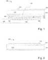
- FIG. 1illustrates schematically a LCOS display panel.
- FIG. 2illustrates schematically a glass structure included in the LCOS display panel.
- FIG. 4illustrates schematically a LCOS display panel, according to an embodiment of the present invention.
- FIG. 5shows an exemplary UV cut filter, which is an interference filter comprising multiple thin films, according to an embodiment of the present invention.
- FIG. 6shows an exemplary spectral transmittance response of the UV cut filter of FIG. 5 , according to an embodiment of the present invention.
- FIG. 7shows an exemplary UV cut filter, which is an interference filter comprising multiple thin films, according to an embodiment of the present invention.
- FIG. 10shows an exemplary UV cut filter, which is an interference filter comprising multiple thin films, according to an embodiment of the present invention.
- FIG. 11shows an exemplary spectral transmittance response of the UV cut filter of FIG. 10 , according to an embodiment of the present invention.
- FIG. 12shows an exemplary UV cut filter, which is an interference filter comprising multiple thin films, according to an embodiment of the present invention.
- FIG. 13shows an exemplary spectral transmittance response of the UV cut filter of FIG. 12 , according to an embodiment of the present invention.
- FIG. 1illustrates schematically a LCOS display panel 100 .
- LCOS display panel 100comprises a silicon substrate 102 having pixel structure 104 formed on silicon substrate 102 and its corresponding electric circuit (not shown) embedded in silicon substrate 102 .
- a first PI (polyimide) layer 106is disposed over pixel structure 104 and surface 108 of silicon substrate 102 .
- First PI layer 106is an alignment layer that aligns the orientation of LC molecules of a LC layer 110 disposed over it.
- FIG. 2illustrates schematically a glass structure 200 comprising a glass substrate 112 .
- An ITO (indium tin oxide) layer 114is coated on a first surface of glass substrate 112 .
- a second PI layer 116is disposed on and attached to ITO layer 114 .
- a second surface opposite to the first surface of glass substrate 112is coated with an AR (anti reflection) layer 118 .
- LCOS display panel 100further comprises glass structure 200 flipped over the position shown in FIG. 2 .
- Second PI layer 116faces first PI layer 106 .
- Second PI layer 116is disposed on LC layer 110 .
- Second PI layer 116aligns the orientation of LC molecules in the vicinity of second PI layer 116
- first PI layer 106aligns the orientation of LC molecules in the vicinity of first PI layer 106 .
- LC layer 110is between first PI layer 106 and second PI layer 116 .
- a dam 120is formed to seal LC material between first PI layer 106 adjacent to silicon substrate 102 and second PI layer 116 adjacent to ITO layer 114 .
- ITO layer 114is disposed on second PI layer 116
- optionally AR layer 118is disposed on glass substrate 112 .
- Dam 120seals the perimeter of LCOS display panel 100 defining a LC reservoir. Dam 120 is disposed between first PI layer 106 and second PI layer 116 and holds silicon substrate 102 and glass substrate 112 together. Dam 120 encloses LC layer 110 within dam 120 . Dam 120 may be made from UV-cure materials, time/temperature cure materials, or photo-patterning materials.
- first and second PI layers 106 and 116 , and LC layer 110that transmit visible light to form a displayed image.
- the UV lightmay age first and second PI layers 106 and 116 , and LC layer 110 , because these layers are made of organic materials containing benzene rings having double bonds. Benzene absorbs UV light, and this will change the characteristics of the LC materials and the PI materials. Upon absorption of UV light, the LC materials and the PI materials suffer from aging and this will affect the life-time of the LCOS display panel 100 .
- FIG. 3illustrates schematically a LCOS display panel 300 , according to an embodiment of the present invention.
- LCOS display panel 300is similar to LCOS display panel 100 of FIG. 1 , except it has an additional UV cut filter 302 .
- UV cut filter 302is preferably an interference filter that reflects an incoming UV light.
- UV cut filter 302is formed on glass substrate 112 between glass substrate 112 and ITO layer 114 .
- UV cut filter 302is disposed on ITO layer 114
- glass substrate 112is disposed on UV cut filter 302 .
- UV cut filter 302covers an active area 310 of LCOS display panel 300 including LC layer 110 and pixel structure 104 . It is appreciated that UV cut filter 310 covers LC layer 110 .
- UV cut filter 302may be formed between ITO layer 114 and second PI layer 116 (not shown).
- the LC layeris more sensitive to UV light as compare with the PI layer.
- active area 310By covering active area 310 from UV exposure, LC layer 110 and the projection light transmitting parts of first PI layer 106 and second PI layer 116 will not be aged, and thus no optical and physical characteristics change.
- An imageis displayed in active area 310 .
- the inclusion of a UV cut filteris also useful for automotive and other applications that may expose the LCOS display panel to sun light or UV light.
- UV light 304transmits through AR layer 118 , glass substrate 112 , ITO layer 114 , second PI layer 116 , dam 120 , first PI layer 106 , and silicon substrate 102 , and UV light 304 is absorbed by dam 120 to UV cure dam 120 .
- No UV cut filter 302is blocking UV light 304 . Accordingly, dam 120 can be UV cured.
- UV light 306 illuminating active area 310is reflected by UV cut filter 302 , and prevented from exposing LC layer 110 , and parts of second PI layer 116 and first PI layer 106 immediately on top and below LC layer 110 , respectively.
- FIG. 4illustrates schematically a LCOS display panel 400 , according to an embodiment of the present invention.
- LCOS display panel 400is similar to LCOS display panel 300 of FIG. 3 , except the following.
- ITO layer 114has the same size as UV cut filter 302 . No UV cut filter 302 and no ITO layer 114 are in the path of UV light 304 . Furthermore, UV cut filter 302 and ITO layer 114 are enclosed in second PI layer 116 attached to glass substrate 112 . Accordingly, no empty space extending from UV cut filter 302 .
- UV light 304transmits through AR layer 118 , glass substrate 112 , second PI layer 116 , dam 120 , first PI layer 106 , and silicon substrate 102 , and UV light 304 is absorbed by dam 120 to UV cure dam 120 .
- No UV cut filter 302 and no ITO layer 114are in the path of UV light 304 . Accordingly, dam 120 can be UV cured.
- first PI layer 106 and second PI layer 116 outside active area 310which is defined by LC layer 110 , are exposed to UV light. It has almost no effect on active area 310 .
- LC layer 110 and the projection light transmitting parts of first PI layer 106 and second PI layer 116will not be aged, and thus no optical and physical characteristics change. Accordingly, it does not affect the performance of LCOS display panel 400 .
- An imageis displayed in active area 310 .
- UV cut filter 302is preferably an interference filter comprising multiple thin films as shown in FIG. 5 .
- FIG. 5shows a multiple thin film structure of an exemplary interference filter according to an embodiment of the present invention.
- the interference filteris made of alternate films of SiO 2 (silicon dioxide) having lower refractive index (1.4585) and Ta 2 O 5 (tantalum pentoxide) having higher refractive index (2.1306) coated on glass substrate 112 .
- the film farthest from glass substrate 112is further coated with ITO layer 114 .
- UV cut filter 302 of FIG. 5An exemplary spectral transmittance response 600 of UV cut filter 302 of FIG. 5 is depicted in FIG. 6 , according to an embodiment of the present invention.
- Spectral response 600shows that UV light having wavelength less than 450 nm is reflected, and visible light having wavelength larger than 465 nm is almost completely transmitted.
- UV cut filter 302 of FIG. 5reflects UV light when dam 120 is UV cured during the manufacture of LCOS display panel 400 , but transmits visible light when LCOS display panel 400 is in operation. Thus LCOS display panel 400 can be used for displaying visible image.
- UV cut filter 302is preferably an interference filter comprising multiple thin films as shown in FIG. 7 .
- FIG. 7shows another multiple thin film structure of an exemplary interference filter, according to an embodiment of the present invention.
- the interference filteris similarly made of alternate films of SiO 2 (silicon dioxide) having lower refractive index (1.4585) and Ta 2 O 5 (tantalum pentoxide) having higher refractive index (2.1306) coated on glass substrate 112 .
- the film farthest from glass substrate 112is further coated with ITO layer 114 .
- FIG. 8An exemplary spectral transmittance response 800 of UV cut filter 302 of FIG. 7 is depicted in FIG. 8 , according to an embodiment of the present invention.
- Spectral response 800shows that UV light having wavelength less than 450 nm is reflected, and SWIR (short wave infra red, 1400-3000 nm) light having wavelength larger than 1400 nm is almost completely transmitted.
- UV cut filter 302 of FIG. 7reflects UV light when dam 120 is UV cured during the manufacture of LCOS display panel 400 , but transmits SWIR light when LCOS display panel 400 is in operation for any applications, such as telecommunications and others.
- FIG. 9illustrates schematically a LCOS display panel 900 , according to an embodiment of the present invention.
- LCOS display panel 900is similar to LCOS display panel 100 of FIG. 1 , except AR layer 118 is removed and replaced with an additional UV cut filter 902 .
- UV cut filter 902is preferably an interference filter that reflects an incoming UV light.
- AR layer 118is replaced with UV cut filter 902 forming on a surface of glass substrate 112 opposite to ITO layer 114 .
- UV cut filter 902covers an active area 310 of LCOS display panel 900 including LC layer 110 and pixel structure 104 . Since no UV cut filter 902 (or 302 ) is between glass substrate 112 and ITO layer 114 , glass substrate 112 is disposed on ITO layer.
- UV light 304can transmit through glass substrate 112 , ITO layer 114 , second PI layer 116 , dam 120 , first PT layer 106 , and silicon substrate 102 , and UV light 304 is absorbed by dam 120 to UV cure dam 120 .
- No UV cut filter 902is in the path of UV light 304 . Accordingly, dam 120 can be UV cured.
- first PI layer 106 and second PI layer 116 outside active area 310which is defined by LC layer 110 , are exposed to UV light. It has almost no effect on active area 310 .
- LC layer 110 and the projection light transmitting parts of first PI layer 106 and second PI layer 116will not be aged, and thus no optical and physical characteristics change. Accordingly, it does not affect the performance of LCOS display panel 900 .
- An imageis displayed in active area 310 .
- UV cut filter 902is preferably an interference filter comprising multiple thin films as shown in FIG. 10 .
- FIG. 10shows a multiple thin film structure of an exemplary interference filter, according to an embodiment of the present invention.
- the interference filteris made of alternate films of SiO 2 (silicon dioxide) having lower refractive index (1.4585) and Ta 2 O 5 (tantalum pentoxide) having higher refractive index (2.1306) coated on glass substrate 112 opposite to ITO layer 114 .
- UV cut filter 902 of FIG. 10An exemplary spectral transmittance response 1100 of UV cut filter 902 of FIG. 10 is depicted in FIG. 11 , according to an embodiment of the present invention.
- Spectral response 1100shows that UV light having wavelength less than 450 nm is reflected, and visible light having wavelength larger than 465 nm is almost completely transmitted.
- UV cut filter 902 of FIG. 10reflects UV light when dam 120 is UV cured during the manufacture of LCOS display panel 900 , but transmits visible light when LCOS display panel 900 is in operation.
- LCOS display panel 900can be used for displaying visible image.
- UV cut filter 902is preferably an interference filter comprising multiple thin films as shown in FIG. 12 .
- FIG. 12shows another multiple thin film structure of an exemplary interference filter, according to an embodiment of the present invention.
- the interference filteris similarly made of alternate films of SiO 2 (silicon dioxide) having lower refractive index (1.4585) and Ta 2 O 5 (tantalum pentoxide) having higher refractive index (2.1306) coated on glass substrate 112 opposite to ITO layer 114 .
- UV cut filter 902 of FIG. 12An exemplary spectral transmittance response 1300 of UV cut filter 902 of FIG. 12 is depicted in FIG. 13 , according to an embodiment of the present invention.
- Spectral response 1300shows that UV light having wavelength less than 450 nm is reflected, and SWIR light having wavelength larger than 1400 nm is almost completely transmitted.
- UV cut filter 902 of FIG. 12reflects UV light when dam 120 is UV cured during the manufacture of LCOS display panel 900 , but transmits SWIR light when LCOS display panel 900 is in operation for any applications, such as telecommunications and others.
Landscapes
- Physics & Mathematics (AREA)
- Nonlinear Science (AREA)
- Optics & Photonics (AREA)
- Crystallography & Structural Chemistry (AREA)
- Chemical & Material Sciences (AREA)
- General Physics & Mathematics (AREA)
- Mathematical Physics (AREA)
- Spectroscopy & Molecular Physics (AREA)
- Engineering & Computer Science (AREA)
- Microelectronics & Electronic Packaging (AREA)
- Liquid Crystal (AREA)
- Devices For Indicating Variable Information By Combining Individual Elements (AREA)
- Electrochromic Elements, Electrophoresis, Or Variable Reflection Or Absorption Elements (AREA)
Abstract
Description
Claims (11)
Priority Applications (3)
| Application Number | Priority Date | Filing Date | Title |
|---|---|---|---|
| US16/057,950US11187933B2 (en) | 2018-08-08 | 2018-08-08 | LCOS display panel having UV cut filter |
| TW108121629ATWI787524B (en) | 2018-08-08 | 2019-06-21 | Lcos display panel having uv cut filter |
| CN201910597870.4ACN110824755B (en) | 2018-08-08 | 2019-07-04 | LCOS display panel with UV cut-off filter |
Applications Claiming Priority (1)
| Application Number | Priority Date | Filing Date | Title |
|---|---|---|---|
| US16/057,950US11187933B2 (en) | 2018-08-08 | 2018-08-08 | LCOS display panel having UV cut filter |
Publications (2)
| Publication Number | Publication Date |
|---|---|
| US20200050051A1 US20200050051A1 (en) | 2020-02-13 |
| US11187933B2true US11187933B2 (en) | 2021-11-30 |
Family
ID=69405795
Family Applications (1)
| Application Number | Title | Priority Date | Filing Date |
|---|---|---|---|
| US16/057,950Active2038-12-11US11187933B2 (en) | 2018-08-08 | 2018-08-08 | LCOS display panel having UV cut filter |
Country Status (3)
| Country | Link |
|---|---|
| US (1) | US11187933B2 (en) |
| CN (1) | CN110824755B (en) |
| TW (1) | TWI787524B (en) |
Families Citing this family (1)
| Publication number | Priority date | Publication date | Assignee | Title |
|---|---|---|---|---|
| CN115421333B (en)* | 2022-09-21 | 2024-07-26 | 豪威半导体(上海)有限责任公司 | LCOS packaging structure and packaging method |
Citations (11)
| Publication number | Priority date | Publication date | Assignee | Title |
|---|---|---|---|---|
| US6111700A (en)* | 1996-09-05 | 2000-08-29 | Fujitsu Limited | Optical display device having a reflection-type polarizer |
| US6219113B1 (en)* | 1996-12-17 | 2001-04-17 | Matsushita Electric Industrial Co., Ltd. | Method and apparatus for driving an active matrix display panel |
| US6288764B1 (en)* | 1996-06-25 | 2001-09-11 | Semiconductor Energy Laboratory Co., Ltd. | Display device or electronic device having liquid crystal display panel |
| US6368732B1 (en)* | 1999-08-23 | 2002-04-09 | Samsung Sdi Co., Ltd. | Light-emitting polymers having high efficiency and color tunable properties |
| US20020154104A1 (en)* | 2000-02-02 | 2002-10-24 | Akira Inoue | Method for driving electrooptical device, driving circuit, and electrooptical device, and electronic apparatus |
| US20050041214A1 (en) | 2003-08-20 | 2005-02-24 | Satoru Kawaai | Liquid-crystal projector |
| US6876412B2 (en) | 2001-04-06 | 2005-04-05 | Sony Corporation | Guest-host liquid crystal element with removable polarizer |
| US20060043318A1 (en) | 2004-08-25 | 2006-03-02 | Nec Lcd Technologies, Ltd. | UV-ray-curing device for curing UV-heat-curable resin in a display panel |
| US20100073613A1 (en)* | 2007-01-26 | 2010-03-25 | Naoshi Yamada | Liquid crystal display panel, liquid crystal display unit, liquid crystal display device, television receiver, and method for manufacturing color filter substrate |
| US20110110207A1 (en)* | 2008-07-28 | 2011-05-12 | Ryuichi Katayama | Optical unit, control method, and optical information recording/reproducing device |
| US8709192B2 (en) | 2005-04-15 | 2014-04-29 | Nitto Denko Corporation | Protective cover sheet comprising a UV-absorbing layer for a polarizer plate and method of making the same |
Family Cites Families (10)
| Publication number | Priority date | Publication date | Assignee | Title |
|---|---|---|---|---|
| JP2002365643A (en)* | 2001-06-06 | 2002-12-18 | Matsushita Electric Ind Co Ltd | Manufacturing method of liquid crystal display element |
| JP2004252027A (en)* | 2003-02-19 | 2004-09-09 | Citizen Watch Co Ltd | Method for manufacturing liquid crystal device, and liquid crystal device |
| JP2011123315A (en)* | 2009-12-11 | 2011-06-23 | Citizen Holdings Co Ltd | Liquid crystal optical element, method for manufacturing the same, and electronic eyeglasses |
| CN102799018A (en)* | 2012-08-09 | 2012-11-28 | 深圳市华星光电技术有限公司 | Liquid crystal display panel and manufacturing method thereof |
| CN102967966B (en)* | 2012-11-20 | 2015-05-20 | 深圳市华星光电技术有限公司 | Liquid crystal display panel and manufacturing method thereof |
| JP5507715B2 (en)* | 2013-02-01 | 2014-05-28 | 株式会社ジャパンディスプレイ | Liquid crystal display |
| CN103217836A (en)* | 2013-04-12 | 2013-07-24 | 深圳市华星光电技术有限公司 | Light mask of liquid crystal display panel and using method of light mask |
| CN104049416A (en)* | 2014-06-23 | 2014-09-17 | 京东方科技集团股份有限公司 | Liquid crystal display screen, manufacturing method of liquid crystal display screen and display device |
| CN105511125B (en)* | 2015-12-30 | 2018-11-09 | 豪威半导体(上海)有限责任公司 | A kind of LCOS display devices and manufacturing method |
| CN108117873A (en)* | 2016-11-29 | 2018-06-05 | 京东方科技集团股份有限公司 | Oriented material composition, liquid crystal display panel and preparation method thereof, display device |
- 2018
- 2018-08-08USUS16/057,950patent/US11187933B2/enactiveActive
- 2019
- 2019-06-21TWTW108121629Apatent/TWI787524B/enactive
- 2019-07-04CNCN201910597870.4Apatent/CN110824755B/enactiveActive
Patent Citations (11)
| Publication number | Priority date | Publication date | Assignee | Title |
|---|---|---|---|---|
| US6288764B1 (en)* | 1996-06-25 | 2001-09-11 | Semiconductor Energy Laboratory Co., Ltd. | Display device or electronic device having liquid crystal display panel |
| US6111700A (en)* | 1996-09-05 | 2000-08-29 | Fujitsu Limited | Optical display device having a reflection-type polarizer |
| US6219113B1 (en)* | 1996-12-17 | 2001-04-17 | Matsushita Electric Industrial Co., Ltd. | Method and apparatus for driving an active matrix display panel |
| US6368732B1 (en)* | 1999-08-23 | 2002-04-09 | Samsung Sdi Co., Ltd. | Light-emitting polymers having high efficiency and color tunable properties |
| US20020154104A1 (en)* | 2000-02-02 | 2002-10-24 | Akira Inoue | Method for driving electrooptical device, driving circuit, and electrooptical device, and electronic apparatus |
| US6876412B2 (en) | 2001-04-06 | 2005-04-05 | Sony Corporation | Guest-host liquid crystal element with removable polarizer |
| US20050041214A1 (en) | 2003-08-20 | 2005-02-24 | Satoru Kawaai | Liquid-crystal projector |
| US20060043318A1 (en) | 2004-08-25 | 2006-03-02 | Nec Lcd Technologies, Ltd. | UV-ray-curing device for curing UV-heat-curable resin in a display panel |
| US8709192B2 (en) | 2005-04-15 | 2014-04-29 | Nitto Denko Corporation | Protective cover sheet comprising a UV-absorbing layer for a polarizer plate and method of making the same |
| US20100073613A1 (en)* | 2007-01-26 | 2010-03-25 | Naoshi Yamada | Liquid crystal display panel, liquid crystal display unit, liquid crystal display device, television receiver, and method for manufacturing color filter substrate |
| US20110110207A1 (en)* | 2008-07-28 | 2011-05-12 | Ryuichi Katayama | Optical unit, control method, and optical information recording/reproducing device |
Also Published As
| Publication number | Publication date |
|---|---|
| TW202013024A (en) | 2020-04-01 |
| CN110824755B (en) | 2024-11-01 |
| US20200050051A1 (en) | 2020-02-13 |
| CN110824755A (en) | 2020-02-21 |
| TWI787524B (en) | 2022-12-21 |
Similar Documents
| Publication | Publication Date | Title |
|---|---|---|
| US10782553B2 (en) | Display device and method of manufacturing the same | |
| US10353248B2 (en) | Electro-optical device and electronic apparatus | |
| US7965370B2 (en) | Liquid crystal display device | |
| WO2000048039A1 (en) | Liquid-crystal display | |
| US9454032B2 (en) | Display device | |
| CN110858045A (en) | Display panel | |
| CN102736340A (en) | Electro-optic device, electronic device, and method of manufacturing electro-optic device | |
| US11187933B2 (en) | LCOS display panel having UV cut filter | |
| CN111584756A (en) | Display panel, display device and packaging method of display panel | |
| JP2016029431A (en) | Electro-optic device, manufacturing method thereof, and electronic apparatus | |
| JP2011215455A (en) | Liquid crystal display device, method for manufacturing the same, and projection display device | |
| JP2008170497A (en) | Liquid crystal display device and manufacturing method thereof | |
| CN105026994A (en) | Liquid crystal device, manufacturing method thereof, and electronic device | |
| US20080074593A1 (en) | Liquid crystal display device and manufacturing method thereof | |
| JP2019039943A (en) | Electro-optical device and electronic apparatus | |
| US10866445B2 (en) | Display device and liquid crystal device | |
| JP6146120B2 (en) | Liquid crystal device and electronic device | |
| JP2015215536A (en) | Electro-optical device and electronic apparatus | |
| JP2004310040A (en) | Peripheral structure of liquid crystal panel | |
| JP7484222B2 (en) | Optical substrate, electro-optical device, electronic device, and method for manufacturing optical substrate | |
| JP7238272B2 (en) | Surface treatment agent, surface treatment method, liquid crystal device and electronic equipment | |
| US10877336B2 (en) | Display panel and method for manufacturing same | |
| JP2009217098A (en) | Liquid crystal device | |
| JP2022190311A (en) | Electro-optical device, method for manufacturing electro-optical device, and electronic apparatus | |
| JP2013025139A (en) | Electro-optic device and electronic equipment |
Legal Events
| Date | Code | Title | Description |
|---|---|---|---|
| AS | Assignment | Owner name:OMNIVISION TECHNOLOGIES, INC., CALIFORNIA Free format text:ASSIGNMENT OF ASSIGNORS INTEREST;ASSIGNORS:FAN, CHUN-SHENG;KO, PEI-WEN;REEL/FRAME:046581/0895 Effective date:20180803 | |
| FEPP | Fee payment procedure | Free format text:ENTITY STATUS SET TO UNDISCOUNTED (ORIGINAL EVENT CODE: BIG.); ENTITY STATUS OF PATENT OWNER: LARGE ENTITY | |
| STPP | Information on status: patent application and granting procedure in general | Free format text:NON FINAL ACTION MAILED | |
| STPP | Information on status: patent application and granting procedure in general | Free format text:NON FINAL ACTION MAILED | |
| STPP | Information on status: patent application and granting procedure in general | Free format text:FINAL REJECTION MAILED | |
| STPP | Information on status: patent application and granting procedure in general | Free format text:NON FINAL ACTION MAILED | |
| STPP | Information on status: patent application and granting procedure in general | Free format text:RESPONSE TO NON-FINAL OFFICE ACTION ENTERED AND FORWARDED TO EXAMINER | |
| STPP | Information on status: patent application and granting procedure in general | Free format text:FINAL REJECTION MAILED | |
| STPP | Information on status: patent application and granting procedure in general | Free format text:DOCKETED NEW CASE - READY FOR EXAMINATION | |
| STPP | Information on status: patent application and granting procedure in general | Free format text:AWAITING TC RESP., ISSUE FEE NOT PAID | |
| STPP | Information on status: patent application and granting procedure in general | Free format text:NOTICE OF ALLOWANCE MAILED -- APPLICATION RECEIVED IN OFFICE OF PUBLICATIONS | |
| STPP | Information on status: patent application and granting procedure in general | Free format text:PUBLICATIONS -- ISSUE FEE PAYMENT VERIFIED | |
| STCF | Information on status: patent grant | Free format text:PATENTED CASE | |
| MAFP | Maintenance fee payment | Free format text:PAYMENT OF MAINTENANCE FEE, 4TH YEAR, LARGE ENTITY (ORIGINAL EVENT CODE: M1551); ENTITY STATUS OF PATENT OWNER: LARGE ENTITY Year of fee payment:4 |