US11186060B2 - Methods of continuous fabrication of holes in flexible substrate sheets and products relating to the same - Google Patents
Methods of continuous fabrication of holes in flexible substrate sheets and products relating to the sameDownload PDFInfo
- Publication number
- US11186060B2 US11186060B2US15/205,284US201615205284AUS11186060B2US 11186060 B2US11186060 B2US 11186060B2US 201615205284 AUS201615205284 AUS 201615205284AUS 11186060 B2US11186060 B2US 11186060B2
- Authority
- US
- United States
- Prior art keywords
- defects
- laser
- substrate sheet
- substrate
- laser beam
- Prior art date
- Legal status (The legal status is an assumption and is not a legal conclusion. Google has not performed a legal analysis and makes no representation as to the accuracy of the status listed.)
- Active, expires
Links
Images


Classifications
- B—PERFORMING OPERATIONS; TRANSPORTING
- B32—LAYERED PRODUCTS
- B32B—LAYERED PRODUCTS, i.e. PRODUCTS BUILT-UP OF STRATA OF FLAT OR NON-FLAT, e.g. CELLULAR OR HONEYCOMB, FORM
- B32B3/00—Layered products comprising a layer with external or internal discontinuities or unevennesses, or a layer of non-planar shape; Layered products comprising a layer having particular features of form
- B32B3/26—Layered products comprising a layer with external or internal discontinuities or unevennesses, or a layer of non-planar shape; Layered products comprising a layer having particular features of form characterised by a particular shape of the outline of the cross-section of a continuous layer; characterised by a layer with cavities or internal voids ; characterised by an apertured layer
- B32B3/266—Layered products comprising a layer with external or internal discontinuities or unevennesses, or a layer of non-planar shape; Layered products comprising a layer having particular features of form characterised by a particular shape of the outline of the cross-section of a continuous layer; characterised by a layer with cavities or internal voids ; characterised by an apertured layer characterised by an apertured layer, the apertures going through the whole thickness of the layer, e.g. expanded metal, perforated layer, slit layer regular cells B32B3/12
- B—PERFORMING OPERATIONS; TRANSPORTING
- B32—LAYERED PRODUCTS
- B32B—LAYERED PRODUCTS, i.e. PRODUCTS BUILT-UP OF STRATA OF FLAT OR NON-FLAT, e.g. CELLULAR OR HONEYCOMB, FORM
- B32B17/00—Layered products essentially comprising sheet glass, or glass, slag, or like fibres
- B32B17/06—Layered products essentially comprising sheet glass, or glass, slag, or like fibres comprising glass as the main or only constituent of a layer, next to another layer of a specific material
- B—PERFORMING OPERATIONS; TRANSPORTING
- B23—MACHINE TOOLS; METAL-WORKING NOT OTHERWISE PROVIDED FOR
- B23K—SOLDERING OR UNSOLDERING; WELDING; CLADDING OR PLATING BY SOLDERING OR WELDING; CUTTING BY APPLYING HEAT LOCALLY, e.g. FLAME CUTTING; WORKING BY LASER BEAM
- B23K26/00—Working by laser beam, e.g. welding, cutting or boring
- B23K26/02—Positioning or observing the workpiece, e.g. with respect to the point of impact; Aligning, aiming or focusing the laser beam
- B23K26/06—Shaping the laser beam, e.g. by masks or multi-focusing
- B23K26/0604—Shaping the laser beam, e.g. by masks or multi-focusing by a combination of beams
- B—PERFORMING OPERATIONS; TRANSPORTING
- B23—MACHINE TOOLS; METAL-WORKING NOT OTHERWISE PROVIDED FOR
- B23K—SOLDERING OR UNSOLDERING; WELDING; CLADDING OR PLATING BY SOLDERING OR WELDING; CUTTING BY APPLYING HEAT LOCALLY, e.g. FLAME CUTTING; WORKING BY LASER BEAM
- B23K26/00—Working by laser beam, e.g. welding, cutting or boring
- B23K26/36—Removing material
- B23K26/38—Removing material by boring or cutting
- B23K26/382—Removing material by boring or cutting by boring
- B23K26/389—Removing material by boring or cutting by boring of fluid openings, e.g. nozzles, jets
- B—PERFORMING OPERATIONS; TRANSPORTING
- B23—MACHINE TOOLS; METAL-WORKING NOT OTHERWISE PROVIDED FOR
- B23K—SOLDERING OR UNSOLDERING; WELDING; CLADDING OR PLATING BY SOLDERING OR WELDING; CUTTING BY APPLYING HEAT LOCALLY, e.g. FLAME CUTTING; WORKING BY LASER BEAM
- B23K26/00—Working by laser beam, e.g. welding, cutting or boring
- B23K26/50—Working by transmitting the laser beam through or within the workpiece
- B23K26/53—Working by transmitting the laser beam through or within the workpiece for modifying or reforming the material inside the workpiece, e.g. for producing break initiation cracks
- B—PERFORMING OPERATIONS; TRANSPORTING
- B23—MACHINE TOOLS; METAL-WORKING NOT OTHERWISE PROVIDED FOR
- B23K—SOLDERING OR UNSOLDERING; WELDING; CLADDING OR PLATING BY SOLDERING OR WELDING; CUTTING BY APPLYING HEAT LOCALLY, e.g. FLAME CUTTING; WORKING BY LASER BEAM
- B23K26/00—Working by laser beam, e.g. welding, cutting or boring
- B23K26/50—Working by transmitting the laser beam through or within the workpiece
- B23K26/55—Working by transmitting the laser beam through or within the workpiece for creating voids inside the workpiece, e.g. for forming flow passages or flow patterns
- C—CHEMISTRY; METALLURGY
- C03—GLASS; MINERAL OR SLAG WOOL
- C03B—MANUFACTURE, SHAPING, OR SUPPLEMENTARY PROCESSES
- C03B33/00—Severing cooled glass
- C03B33/02—Cutting or splitting sheet glass or ribbons; Apparatus or machines therefor
- C03B33/0222—Scoring using a focussed radiation beam, e.g. laser
- C—CHEMISTRY; METALLURGY
- C03—GLASS; MINERAL OR SLAG WOOL
- C03C—CHEMICAL COMPOSITION OF GLASSES, GLAZES OR VITREOUS ENAMELS; SURFACE TREATMENT OF GLASS; SURFACE TREATMENT OF FIBRES OR FILAMENTS MADE FROM GLASS, MINERALS OR SLAGS; JOINING GLASS TO GLASS OR OTHER MATERIALS
- C03C15/00—Surface treatment of glass, not in the form of fibres or filaments, by etching
- C—CHEMISTRY; METALLURGY
- C03—GLASS; MINERAL OR SLAG WOOL
- C03C—CHEMICAL COMPOSITION OF GLASSES, GLAZES OR VITREOUS ENAMELS; SURFACE TREATMENT OF GLASS; SURFACE TREATMENT OF FIBRES OR FILAMENTS MADE FROM GLASS, MINERALS OR SLAGS; JOINING GLASS TO GLASS OR OTHER MATERIALS
- C03C17/00—Surface treatment of glass, not in the form of fibres or filaments, by coating
- C03C17/06—Surface treatment of glass, not in the form of fibres or filaments, by coating with metals
- H—ELECTRICITY
- H01—ELECTRIC ELEMENTS
- H01L—SEMICONDUCTOR DEVICES NOT COVERED BY CLASS H10
- H01L21/00—Processes or apparatus adapted for the manufacture or treatment of semiconductor or solid state devices or of parts thereof
- H01L21/02—Manufacture or treatment of semiconductor devices or of parts thereof
- H01L21/04—Manufacture or treatment of semiconductor devices or of parts thereof the devices having potential barriers, e.g. a PN junction, depletion layer or carrier concentration layer
- H01L21/48—Manufacture or treatment of parts, e.g. containers, prior to assembly of the devices, using processes not provided for in a single one of the groups H01L21/18 - H01L21/326 or H10D48/04 - H10D48/07
- H01L21/4814—Conductive parts
- H01L21/4846—Leads on or in insulating or insulated substrates, e.g. metallisation
- H01L21/486—Via connections through the substrate with or without pins
- H—ELECTRICITY
- H01—ELECTRIC ELEMENTS
- H01L—SEMICONDUCTOR DEVICES NOT COVERED BY CLASS H10
- H01L23/00—Details of semiconductor or other solid state devices
- H01L23/12—Mountings, e.g. non-detachable insulating substrates
- H01L23/14—Mountings, e.g. non-detachable insulating substrates characterised by the material or its electrical properties
- H01L23/15—Ceramic or glass substrates
- H—ELECTRICITY
- H01—ELECTRIC ELEMENTS
- H01L—SEMICONDUCTOR DEVICES NOT COVERED BY CLASS H10
- H01L23/00—Details of semiconductor or other solid state devices
- H01L23/48—Arrangements for conducting electric current to or from the solid state body in operation, e.g. leads, terminal arrangements ; Selection of materials therefor
- H01L23/488—Arrangements for conducting electric current to or from the solid state body in operation, e.g. leads, terminal arrangements ; Selection of materials therefor consisting of soldered or bonded constructions
- H01L23/498—Leads, i.e. metallisations or lead-frames on insulating substrates, e.g. chip carriers
- H01L23/49827—Via connections through the substrates, e.g. pins going through the substrate, coaxial cables
- B—PERFORMING OPERATIONS; TRANSPORTING
- B23—MACHINE TOOLS; METAL-WORKING NOT OTHERWISE PROVIDED FOR
- B23K—SOLDERING OR UNSOLDERING; WELDING; CLADDING OR PLATING BY SOLDERING OR WELDING; CUTTING BY APPLYING HEAT LOCALLY, e.g. FLAME CUTTING; WORKING BY LASER BEAM
- B23K2103/00—Materials to be soldered, welded or cut
- B23K2103/50—Inorganic material, e.g. metals, not provided for in B23K2103/02 – B23K2103/26
- B23K2103/52—Ceramics
- B—PERFORMING OPERATIONS; TRANSPORTING
- B23—MACHINE TOOLS; METAL-WORKING NOT OTHERWISE PROVIDED FOR
- B23K—SOLDERING OR UNSOLDERING; WELDING; CLADDING OR PLATING BY SOLDERING OR WELDING; CUTTING BY APPLYING HEAT LOCALLY, e.g. FLAME CUTTING; WORKING BY LASER BEAM
- B23K2103/00—Materials to be soldered, welded or cut
- B23K2103/50—Inorganic material, e.g. metals, not provided for in B23K2103/02 – B23K2103/26
- B23K2103/54—Glass
- B—PERFORMING OPERATIONS; TRANSPORTING
- B32—LAYERED PRODUCTS
- B32B—LAYERED PRODUCTS, i.e. PRODUCTS BUILT-UP OF STRATA OF FLAT OR NON-FLAT, e.g. CELLULAR OR HONEYCOMB, FORM
- B32B2307/00—Properties of the layers or laminate
- B32B2307/40—Properties of the layers or laminate having particular optical properties
- B32B2307/412—Transparent
- Y—GENERAL TAGGING OF NEW TECHNOLOGICAL DEVELOPMENTS; GENERAL TAGGING OF CROSS-SECTIONAL TECHNOLOGIES SPANNING OVER SEVERAL SECTIONS OF THE IPC; TECHNICAL SUBJECTS COVERED BY FORMER USPC CROSS-REFERENCE ART COLLECTIONS [XRACs] AND DIGESTS
- Y02—TECHNOLOGIES OR APPLICATIONS FOR MITIGATION OR ADAPTATION AGAINST CLIMATE CHANGE
- Y02P—CLIMATE CHANGE MITIGATION TECHNOLOGIES IN THE PRODUCTION OR PROCESSING OF GOODS
- Y02P40/00—Technologies relating to the processing of minerals
- Y02P40/50—Glass production, e.g. reusing waste heat during processing or shaping
- Y02P40/57—Improving the yield, e-g- reduction of reject rates
Definitions
- Glasshas many advantages over traditional crystalline silicon and organic substrates for use as electrical interposer substrates in semiconductor applications.
- One advantage of glassis that it may be fabricated in a large flat panel format—i.e., in sizes well in excess of traditional 300 mm wafer sizes, even up to many meters on a side.
- Yet another advantage of glassis its high electrical impedance. This is especially helpful at higher frequencies, in particular for the radio frequencies (RF) employed for high data transmission rates.
- RFradio frequencies
- specialty glass substratescan be formed, such as via a fusion forming process, with very flat and smooth surfaces, reducing or eliminating any need for costly polishing steps. This low roughness, or surface quality, of the glass sheets allows them to be patterned with dense (closed spaced) electrical traces.
- glass wafersare simply as carrier substrates on which thin silicon wafers are affixed and processed.
- Other usesinclude the use of glass wafers to form substrates for RF components or for electrical interposers.
- Interposersfor example, provide an interconnecting board that routes electrical signals between two electrical processing chips, such as between a CPU (central processing unit) and another CPU, or between a CPU and a GPU (graphical processing unit), or between a CPU and other devices underneath.
- the waferneeds to have many (e.g., approximately hundreds of thousands or more) holes in it at application specific locations.
- metal tracesare patterned on the glass surfaces and the interior of the holes are metallized in an equally precise manner using lithography and metal vapor deposition or electroplating.
- the glasscan be incorporated into a circuit board and chips are bonded to it. Later, the wafer is diced to separate out the individual components.
- Traditional glass interposersare formed from wafers that have already been cut to the desired size and shape. These wafers are loaded into a laser system. These laser systems may use mechanical fixtures or vision alignment to align to edges of the wafers or other fiducials on the wafers. The laser process then creates the desired hole pattern within the wafers. The wafers are then unloaded. This is a one-at-a-time type operation. This process flow leads to a number of manufacturing inefficiencies.
- Inventory managementcan be problematic. There are numerous wafer sizes and shapes (100,150, 200, 300 mm diameters, with notches, flats, etc., panels of various dimensions, each of different compositions or thicknesses) desired by end users, and all of these must be made ahead of time and kept in sufficient quantities in inventory.
- Pattern accuracye.g., the precision of hole placement relative to the edges of the wafers, is also less than optimal. Since the wafers are generally cut with a mechanical score and break process and then undergo an edge grind process, the accuracy to which the geometry and sizes of the wafers are made is generally ⁇ 100 microns or greater. This in turn leads to variability in where the hole pattern is placed relative to the geometric edges of the wafer. This uncertainty cascades into increased alignment complexity needed in order to locate hole patterns in downstream processes such as lithographic steps for metal trace patterning.
- the cost of cutting and finishing the waferscan also be significant. While mechanical score and break equipment is relatively inexpensive, the time and cost of grinding the edges of the wafers to the exact shape desired can be large (e.g., many tens of dollars/wafer) because of the amount of material removal needed and also because the facilities with such cut and grind capabilities are not always co-located with the interposer drilling process equipment.
- a primary purpose of the mechanical edge grindingis to remove damage from the mechanical cutting process, improving the reliability or strength of the wafers edges so that the wafers can survive shipment and downstream process handling.
- the wafer edgesdo not serve a function in the final interposer/chip application, as the interposer dies are cut out of the wafers and hence any finished edges are thrown away. Thus, the true requirement for wafer edges is merely to have sufficient strength and reliability to be handled.
- a lasere.g., a pulsed laser
- an optical systemto generate a line focus of the laser beam within the target substrate, such as a glass substrate sheet.
- the pulsed laser cutting and drilling system and processcreates holes or defects that, in certain embodiments, extend the full depth of the glass sheet with each individual laser burst pulse, and allows the laser system to cut and separate the target substrate into any desired contour by creating a series of perforations that form a contour or desired part shape. Since a glass substrate sheet is brittle, cracking will then follow the perforated contour, allowing the glass substrate sheet to separate into any required shape defined by the perforations.
- a process of fabricating a substrateincludes disposing a substrate sheet at a laser processing assembly.
- the laser processing assemblyincludes at least one laser operable to emit a laser beam.
- the substrate sheetis substantially transparent to the laser beam.
- the processfurther includes focusing the laser beam into a laser beam focal line, viewed along a beam propagation direction of the laser beam.
- the laser beam focal lineis directed into the substrate and generates an induced absorption within the substrate.
- the induced absorptionproduces a defect along the laser beam focal line within the substrate sheet.
- the substrateis translated relative to the laser beam to laser drill a plurality of internal defects within the substrate.
- a first plurality of defects and a second plurality of defectsare created.
- the second plurality of defectsdefines a closed boundary, and the first plurality of defects is disposed within the closed boundary. At least one component piece of the substrate is separated along the closed boundary defined by the second plurality of defects.
- the substrateis selected from the group consisting of a glass substrate sheet, a glass-ceramic substrate sheet, fused silica, and a sapphire sheet.
- the second plurality of defectshave a pitch of less than about 20 um between defects.
- the first plurality of defectsare less than about 10 um in diameter and extend greater than about 100 um in depth.
- the first plurality of defectscomprises holes having a diameter between about 10 um and 120 um and extending through the substrate.
- a seventh aspect according to the sixth aspectfurther comprising metallizing the first plurality of defect holes extending through the substrate.
- the operation of separating the component piece along the boundary defined by the second plurality of external defectsprovides a serrated edge along at least one side of the component piece.
- the serrated edgeis formed by the second plurality of defects of the closed boundary, wherein an amplitude of the serration is less than about 10 um and a pitch of the serrations is less than about 20 um.
- the operation of separating the component piece along the boundary defined by the plurality of external defectsis performed using an infrared laser.
- the operation of creating the first plurality of defectsis performed prior to the operation of creating the second plurality of defects.
- the operation of creating the second plurality of defectsis performed prior to the operation of creating the first plurality of defects.
- a first optical headis adapted to provide the first plurality of defects and a second optical head is adapted to provide the second plurality of defects.
- the operation of providing the substrate disposed at a laser processing assemblycomprises providing the substrate disposed about a roll.
- the laser beamcomprises a pulsed laser beam.
- the substratehas an absorption or scattering of a wavelength of the laser beam of less than about 10%.
- the laser beamhas an average laser burst pulse energy measured at the material greater than about 40 ⁇ J, pulses having a duration in a range of between greater than about 1 picosecond and less than about 100 picoseconds, and a repetition rate in a range of between about 100 Hz and about 1 MHz.
- a plurality of component piecesare defined by a plurality of sets of the second plurality of defects that each define a closed boundary and a plurality of the first plurality of defects are disposed within each closed boundary.
- an articlein a twentieth aspect, includes a substrate having a first side and an opposing second side.
- the substratehas an absorption or scattering of a wavelength of a laser beam of less than about 20%.
- a first plurality of defectsis formed internal to a boundary of the substrate that extend into the substrate.
- a boundary edgeis formed by a second plurality of defects and a plurality of micro cracks extending between the second plurality of defects.
- the second plurality of defectsis spaced from each other at a pitch less than about 20 ⁇ m.
- the second plurality of defectseach have a width of less than about 10 um and extend through at least about 50% of a thickness of the substrate.
- each of the second plurality of defectsextend through the entire thickness of the glass substrate layer.
- the substratecomprises greater than 1,000 first plurality of defects formed within a boundary defined by the second plurality of defects and the first plurality of defects each have a diameter of less than about 3 um.
- the substratecomprises greater than 1,000 first plurality of defects formed within a boundary defined by the second plurality of defects and the first plurality of defects each have a diameter of greater than about 5 um and less than about 120 um.
- the first plurality of defectscomprise a plurality of blind holes.
- an electrically conductive pathis formed by a metallization layer extending through the first plurality of holes.
- a plurality of component piecesare defined from the substrate by a plurality of sets of the second plurality of defects that each define a closed boundary and a plurality of the first plurality of defects are disposed within each closed boundary.
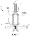
- FIG. 1is a schematic illustration of an example optical system adapted to process a substrate using a laser beam according to one or more embodiments described and illustrated herein;
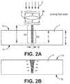
- FIG. 2Ais a schematic illustration of example laser processing components of a laser processing assembly to form defects within the substrate sheets according to one or more embodiments described and illustrated herein;
- FIG. 2Bis a schematic illustration of a side view of a substrate sheet depicting the formation of a defect line due to the induced absorption along a focal line created by the laser processing components depicted in FIG. 2A according to one or more embodiments described and illustrated herein;
- FIG. 3is a schematic illustration of example laser processing components of a laser processing assembly to form defects within the substrate sheets according to one or more embodiments described and illustrated herein;
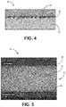
- FIG. 4an example microscope image of a substrate showing a crack connecting laser formed defects or perforations according to one or more embodiments described and illustrated herein;
- FIG. 5shows an example scanning electron microscope (SEM) image showing a characteristic edge resulting from one or more laser line focus cutting process embodiments according to one or more embodiments described and illustrated herein;
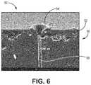
- FIG. 6shows the example SEM image of the entrance side of an individual defect in a glass substrate, such as may be formed by one or more laser line focus cutting process according to one or more embodiments described and illustrated herein;
- FIG. 7shows example pre-etch and post-etch microscope images of a glass substrate according to one or more embodiments described and illustrated herein;
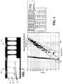
- FIG. 8shows example Weibull plots of the resultant edge strength, measured on 130 um thick Eagle XG glass, using a two-point bend test method according to one or more embodiments described and illustrated herein;
- FIG. 9shows example results of a process study for drilling an example glass substrate, where the pulse energy and the focal length of the final objective lens were varied to show effects according to one or more embodiments described and illustrated herein;
- FIG. 10shows an example chart illustrating results of the study shown in FIG. 9 according to one or more embodiments described and illustrated herein;
- FIG. 11schematically shows an example laser system employing two optical heads according to one or more embodiments described and illustrated herein;
- FIG. 12shows a flow chart of an example process of fabricating a substrate using a focus line laser and/or a short pulse laser to fabricate the substrate according to one or more embodiments described and illustrated herein;
- FIGS. 13 and 14schematically show multiple wafers and panels with one or more desired patterns created out of a single larger panel according to one or more embodiments described and illustrated herein;
- FIG. 15schematically depicts an example layout where one sheet of glass is being cut into four different sizes with two different patterns according to one or more embodiments described and illustrated herein;
- FIG. 16schematically shows another example layout where multiple subpanels that contain wafers with a desired pattern can be created out of a single larger panel according to one or more embodiments described and illustrated herein;
- FIG. 17schematically shows an example process and system for laser fabricating a substrate sheet according to one or more embodiments described and illustrated herein;
- FIG. 18schematically shows a roll to roll process for fabricating a substrate sheet according to one or more embodiments described and illustrated herein;
- FIG. 19Ais a schematic illustration of an example etching assembly according to one or more embodiments described and illustrated herein;
- FIG. 19Bis a schematic illustration of an example etching assembly according to one or more embodiments described and illustrated herein;
- FIG. 19Cis a schematic illustration of an example etching assembly according to one or more embodiments described and illustrated herein;
- FIG. 20Ais a schematic illustration of a partial view of a substrate sheet after fabrication of holes according to one or more embodiments described herein;
- FIG. 20Bis a schematic illustration of a partial view of a substrate sheet after metallizing the holes of FIG. 20A according to one or more embodiments described herein;
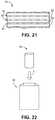
- FIG. 21is a schematic illustration of a partial view of a spool comprising a substrate sheet and an interleaf layer according to one or more embodiments described herein;
- FIG. 22is a schematic illustration of a spool comprising a substrate sheet and an interleaf layer being positioned within an etching assembly according to one or more embodiments described and illustrated herein.
- a first plurality of defects and a second plurality of defectsare created.
- the second plurality of defectsdefines a closed boundary, and the first plurality of defects is disposed within the closed boundary.
- At least one component piece of the substrateis separated along the closed boundary defined by the second plurality of defects.
- a system and process of cutting and drilling in a target substrateuses a pulsed laser and an optical system to generate a line focus of the laser beam within the target substrate, such as a glass substrate sheet.
- the pulsed laser cutting and drilling system and processcreates holes or defects that, in certain embodiments, extend the full depth of the glass sheet with each individual laser pulse, and allows the laser system to cut and separate the target substrate into any desired contour by creating a series of perforations that form a contour or desired part shape. Since a glass substrate sheet is brittle, cracking will then follow the perforated contour, allowing the glass substrate sheet to separate into any required shape defined by the perforations.
- the system and processcan cut a multitude of glass compositions, ranging from high stress glasses (e.g.
- the system and processcan further be adapted to make desired pilot hole patterns in glass wafers.
- An acid etch processmay also be used to enlarge the holes.
- the resulting articlecan then be used for applications where a glass substrate with vias could be used, including, but not limited to, interposers, substrates for RF components, or substrates for fingerprint sensors.
- the systems and processes described hereinsolve the above mentioned problems by combining both the cutting of the glass part with the creation of the desired internal hole pattern in one line focus pulsed laser platform.
- the same laser beam delivery system that creates a first set of defects, such as pilot hole patternscan also be used to create a second set of defects adapted to perforate and separate (i.e. cut) the larger substrates (e.g., glass sheet substrates) into wafers, panels, or sub-panels.
- a userloads a glass panel of appropriate thickness and glass composition into the system, and the output is fully cut parts (e.g. wafers or sub-panels) with pilot hole patterns (first set of defects) that can be etched in a subsequent process step.
- a substratemay be cut into individual components along a boundary or perimeter formed by the second set of defects and then a first set of defects (e.g., pilot holes) may be drilled or otherwise formed in the individual components in a separate step after the substrate has been cut into various component pieces along the boundary or perimeter formed by the second set of defects.
- drilling the first set of defectsmay be performed via a focus line laser process or any other acceptable drilling process.
- other processes of cutting a substrate into individual components along a boundary or perimeter formed by the second set of defects and a focus line laser processmay be used to drill or otherwise process the individual components to create a first set of defects (e.g., pilot holes, vias or interposers) after they have been cut into pieces.
- the line focus and short pulse laser process described hereinis unique in that it allows for both cutting and drilling of substrates, such as glass substrates, with high speed (hundreds of mm/sec to greater than 1 m/sec cutting, hundreds or thousands of holes/sec drilling or greater), and/or with suitable quality (edge strength greater than 100 MPa, low sub-surface damage of less than 100 microns, holes with diameter as small as 5 microns, holes with no surface chips and/or parts that retains strength of greater than 90% as compared to undrilled glass substrates).
- laser generated defectsallow for cutting substrates (e.g., glass sheet substrates) around a boundary or perimeter of a part using defects/perforations and fabricating holes on an interior of a part by etching out the defects/perforations to make holes.
- substratese.g., glass sheet substrates
- Embodiments described hereindetail how the cutting and drilling processes may be employed in a single laser system to make glass interposer parts very efficiently and accurately, or, even if done by multiple systems, used to make glass interposer parts more cost effectively than with other methods.
- Typical laser machining processesuse a Gaussian, or approximately Gaussian, laser beams focused to a spot (or point).
- a Gaussian, or approximately Gaussian, laser beamsfocused to a spot (or point).
- a very small regiontypically microns in diameter
- a beamwill diffract or spread out very quickly, typically within tens of microns. This means that only a very small portion of the glass can be modified by each laser pulse.
- the focus line laser and short pulse laser processes described hereinemploy optics that create an extended focus, or line focus.
- An example of an optical system 10 adapted for creating such a line focusis illustrated in FIG. 1 .
- an example optical system 10 adapted to process a substrate 12 , such as a glass substrate, using a laser beam 14is schematically illustrated.
- the optical system 10is adapted to produce a line focus 16 for the laser beam 14 on the substrate 12 .
- the line focus 16 of the laser beam 14can be adapted to fabricate defects or perforations (e.g., the second set of defects described above) oriented to allow for cutting the substrate 12 along a boundary or perimeter of the defects or perforations and/or for fabricating a first set of defects to provide holes within the substrate 12 disposed within the boundary or perimeter of the second set of defects or perforations.
- the optical system 10is adapted to focus the laser beam 14 (e.g., a pulsed laser beam) into a laser beam focal line 16 oriented along the beam propagation direction.
- the substrate 12e.g., a glass substrate sheet
- the substrate 12is substantially transparent to the laser wavelength when the absorption is less than about 10%, in some examples less than about 1% per mm of material depth at this wavelength.
- a laseremits laser beam 14 , which has a portion incident to the optical assembly 10 .
- the optical assembly 10turns the incident laser beam into an extensive laser beam focal line 16 on an output side of the optical system 10 over a defined expansion range along the beam direction.
- the planar substrate 12e.g., the glass substrate sheet
- the laser beam focal line 16is thus directed into the substrate 12 .
- an incident Gaussian beam from a laseris passed through an axicon 18 (a conical optical element), which creates a line focus.
- the line focuscan be propagated or re-imaged through other standard optical elements such as lenses that form a telescope in order to project it to another location and also alter its spatial extent. This is sometimes referred to as creating a Bessel beam, or more specifically a Gauss-Bessel beam.
- Such a beamdiffracts much more slowly than a Gaussian beam, allowing a central region (approximately a few microns in diameter) of very high optical intensity to be maintained over very long ranges (approximately millimeters).
- Other solutionsalso are possible that form an extended line focus, which in a broader context is often referred to as non-diffracting beams.
- an axicon 18disperses at least a portion of the laser beam 14 incident to the optical assembly 10 toward a first lens 20 .
- the first lens 20collimates the dispersed laser beam 14 within the optical assembly 10 toward a second lens 22 .
- the second lens 22receives the collimated portion of the laser beam 14 and focuses the beam 14 toward the substrate 12 to focus the beam into a laser beam focal line 16 .
- the line focusis used in conjunction with very high pulse energy short pulsed laser (e.g., less than 10 ps pulse width, approximately 50 to 500 uJ/burst).
- very high pulse energy short pulsed lasere.g., less than 10 ps pulse width, approximately 50 to 500 uJ/burst.
- Many short pulse lasersallow a mode of operation called “burst” pulse mode.
- a “burst” pulseis a sequence of pulses that are closely spaced in time (e.g. 20 nsec), whereas the time between each “burst” may be longer, such as 10 usec. Since the gain medium for such lasers has a fixed amount of energy that can be extracted on a short time scale, typically the total energy within a burst is conserved, i.e.
- the substrateis substantially transparent to the radiation (typically ⁇ 10% absorption per mm), otherwise the energy will be absorbed at or near the surface of the glass and not reach the interior to form a line.
- the wavelength of the laseris approximately 1064 nm, which can be produced by a Nd:YVO 4 laser or similar (e.g.
- YAGYAG gain material
- various harmonics of this wavelengthmay also be used, such as approximately 532 nm (doubled frequency), or approximately 355 nm (tripled frequency). These harmonics are easily available by employing non-linear conversion crystal(s) at the output of the laser head.
- the result in the transparent substrateis very similar to the effect of perforating paper.
- the perforationsremove very little material, but are capable of guiding a tear or crack that ultimately separates the substrate. If these defects are spaced close together, cracks form to interconnect the defects.
- One advantage of this processis that very little material is removed, and therefore, very little debris is generated.
- the substratehas enough stress in it, as in the case of many ion-exchanged glasses, cracks will propagate from one defect site to another without the need for any further process steps. But if the substrate has low stress, such as in the case of display glasses such as Corning Eagle XG or pre-ion exchange glasses, then further stress can be applied to fully form the cracks between the damage sites. In one embodiment, for example, this can be done by tracing the same perforated (defect) pattern using an infrared laser, such as a carbon dioxide (CO 2 ) laser. This creates a thermal stress that enhances the propagation of the crack, resulting in two separate pieces. An image showing glass that has defects created but has not yet been separated is shown in FIG. 4 . An image showing the resulting edge post-separation is shown in FIG. 5 .
- an infrared lasersuch as a carbon dioxide (CO 2 ) laser.
- FIGS. 2A and 2Banother embodiment of an optical system and method of laser processing a material includes focusing a pulsed laser beam 2 into a laser beam focal line 2 b oriented along the beam propagation direction.
- the substrate 1e.g., a glass substrate sheet
- the substrate 1is substantially transparent to the laser wavelength when the absorption is less than about 10%, preferably less than about 1% per mm of material depth at this wavelength.
- laser(not shown) emits laser beam 2 , which has a portion 2 a incident to an optical assembly 6 .
- the optical assembly 6turns the incident laser beam into an extensive laser beam focal line 2 b on the output side of the optical assembly 6 over a defined expansion range along the beam direction (length 1 of the focal line).
- the planar substrate 1is positioned in the beam path to at least partially overlap the laser beam focal line 2 b of laser beam 2 .
- the laser beam focal lineis thus directed into the substrate.
- Reference 1 adesignates the surface of the planar substrate facing the optical assembly 6 or the laser, respectively, and reference lb designates the reverse surface of substrate 1 .
- the substrate or material thickness(in this embodiment measured perpendicularly to the planes 1 a and 1 b , i.e., to the substrate plane) is labeled with d.
- substrate 1is aligned perpendicular to a longitudinal beam axis and thus behind the same focal line 2 b produced by the optical assembly 6 (the substrate is perpendicular to the plane of the drawing).
- the focal linebeing oriented or aligned along the beam direction, the substrate is positioned relative to the focal line 2 b in such a way that the focal line 2 b starts before the surface 1 a of the substrate and stops before the surface lb of the substrate, i.e. still focal line 2 b terminates within the substrate and does not extend beyond surface 1 b .
- the extensive laser beam focal line 2 bIn the overlapping area of the laser beam focal line 2 b with substrate 1 , i.e., in the substrate material covered by focal line 2 b , the extensive laser beam focal line 2 b generates (assuming suitable laser intensity along the laser beam focal line 2 b , which intensity is ensured by the focusing of laser beam 2 on a section of length 1 , i.e. a line focus of length 1 ) an extensive section 2 c (aligned along the longitudinal beam direction) along which an induced absorption is generated in the substrate material.
- the induced absorptionproduces defect line formation in the substrate material along section 2 c .
- the defect lineis a microscopic (e.g., >100 nm and ⁇ 0.5 micron in diameter) elongated “hole” (also called a perforation or a defect line) in the substrate using a single high energy burst pulse.
- Individual defect linescan be created at rates of several hundred kilohertz (several hundred thousand defect lines per second), for example. With relative motion between the source and the substrate, these holes can be placed adjacent to one another (spatial separation varying from sub-micron to many microns as desired).
- the defect line formationis not only local, but over the entire length of the extensive section 2 c of the induced absorption.
- the length of section 2 c(which corresponds to the length of the overlapping of laser beam focal line 2 b with substrate 1 ) is labeled with reference L.
- the average diameter or extent of the section of the induced absorption 2 c (or the sections in the material of substrate 1 undergoing defect line formation)is labeled with reference D.
- This average extent Dbasically corresponds to the average diameter 6 of the laser beam focal line 2 b , that is, an average spot diameter in a range of between about 0.1 micron and about 5 microns.
- FIG. 2Ashows, the substrate material (which is transparent to the wavelength ⁇ of laser beam 2 ) is heated due to the induced absorption along the focal line 2 b arising from the nonlinear effects associated with the high intensity of the laser beam within focal line 2 b .
- FIG. 2Billustrates that the heated substrate material will eventually expand so that a corresponding induced tension leads to micro-crack formation, with the tension being the highest at surface 1 a.
- MPAmulti-photon absorption
- MPAis the simultaneous absorption of two or more photons of identical or different frequencies in order to excite a molecule from one state (usually the ground state) to a higher energy electronic state (ionization).
- the energy difference between the involved lower and upper states of the moleculecan be equal to the sum of the energies of the two or more photons.
- MPAalso called induced absorption, can be a third-order process, for example, that is several orders of magnitude weaker than linear absorption.
- MPAdiffers from linear absorption in that the strength of induced absorption can be proportional to the square or cube of the light intensity, for example, instead of being proportional to the light intensity itself
- MPAis a nonlinear optical process.
- optical assemblies 6which can be applied to generate the focal line 2 b , as well as a representative optical setup, in which these optical assemblies can be applied, are described below. Identical references are used for identical components or features or those which are equal in their function.
- the laser beammust illuminate the optics up to the required aperture, which is typically achieved by means of beam widening using widening telescopes between the laser and focusing optics.
- the spot sizeshould not vary too strongly for the purpose of a uniform interaction along the focal line. This can, for example, be ensured (see the embodiment below) by illuminating the focusing optics only in a small, circular area so that the beam opening and thus the percentage of the numerical aperture only vary slightly.
- FIG. 3section perpendicular to the substrate plane at the level of the central beam in the laser beam bundle of laser radiation 2 ; here, too, laser beam 2 is perpendicularly incident to the substrate plane, i.e. incidence angle is 0° so that the focal line 2 b or the extensive section of the induced absorption 2 c is parallel to the substrate normal
- the laser radiation 2 a emitted by the laseris first directed onto a circular aperture 8 which is completely opaque to the laser radiation used.
- Aperture 8is oriented perpendicular to the longitudinal beam axis and is centered on the central beam of the depicted beam bundle 2 a.
- the diameter of aperture 8is selected in such a way that the beam bundles near the center of beam bundle 2 a or the central beam (here labeled with 2 a Z) hit the aperture and are completely absorbed by it. Only the beams in the outer perimeter range of beam bundle 2 a (marginal rays, here labeled with 2 a R) are not absorbed due to the reduced aperture size compared to the beam diameter, but pass aperture 8 laterally and hit the marginal areas of the focusing optic elements of the optical assembly 6 , which, in this embodiment, is designed as a spherically cut, bi-convex lens 7 .
- the laser beam focal line 2 bis not only a single focal point for the laser beam, but rather a series of focal points for different rays in the laser beam.
- the series of focal pointsform an elongated focal line of a defined length, shown in FIG. 3 as the length 1 of the laser beam focal line 2 b .
- Lens 7is centered on the central beam and in this embodiment is designed as a non-corrected, bi-convex focusing lens in the form of a common, spherically cut lens. The spherical aberration of such a lens may be advantageous.
- aspheres or multi-lens systems deviating from ideally corrected systemswhich do not form an ideal focal point but a distinct, elongated focal line of a defined length, can also be used (i.e., lenses or systems which do not have a single focal point).
- the zones of the lensthus focus along a focal line 2 b , subject to the distance from the lens center.
- the diameter of aperture 8 across the beam directionis approximately 90% of the diameter of the beam bundle (defined by the distance required for the intensity of the beam to decrease to 1/e 2 of the peak intensity) and approximately 75% of the diameter of the lens of the optical assembly 6 .
- FIG. 3shows the section in one plane through the central beam, and the complete three-dimensional bundle can be seen when the depicted beams are rotated around the focal line 2 b.
- U.S. Pub. No. 2015/0166396discloses additional embodiments for creating the laser focal line for drilling holes into substrates that may be utilized. It should also be understood that other laser drilling methods that do not use a laser focal line may also be utilized.
- FIG. 4depicts an example microscope image 30 of a substrate 32 showing a crack 34 connecting laser formed defects 36 or perforations.
- the crack 34 and laser formed defectsmay be used to cut or score the substrate 32 .
- a pitch between defects in a glass substratemay be less than 10 ⁇ m, although other measurements are contemplated and may vary depending on characteristics of any given substrate.
- the defects 36 or perforationsmay be disposed generally in a closed boundary or perimeter around a desired shape of a component and provide the second set of defects described above to cut or score the substrate 32 into one or more component(s).
- the closed boundarymay comprise a closed boundary formed entirely by the second set of defects and cracks connecting them or may be formed by a combination of the second set of defects and one or more edges of the overall substrate 32 where components formed from the substrate include edges in common with the overall substrate 32 .
- FIG. 5shows an example scanning electron microscope (SEM) image 40 showing a characteristic edge 42 resulting from one or more laser line focus cutting process embodiments described herein.
- SEMscanning electron microscope
- Such a corrugated or perforated edgehas unique characteristics. To the eye, it has a frosted or lightly polished appearance. When viewed under a microscope, the edge can easily be characterized by the striations which are created from the line defects, giving the edge a corrugated texture. The pitch of these line defects determines the spacing of the striations. Again, these can easily been seen with an optical microscope.
- the edgehas many desirable properties, including low sub-surface damage extending into the cut piece (e.g., typically less than 100 microns), good and extremely consistent edge strength (e.g., typically greater than 100 MPa, often greater than 150 MPa; with a variance often less than 10 MPa), and a 90 degree profile.
- an example SEM image 50shows what the defects or perforations look like where the laser beam enters the glass. These defects or damage tracks (or pilot holes) are very small, on order of a 350 nm diameter. These defects can be enlarged using further processing with chemical etching to create micron sized holes. Side profiles of such perforations or holes are shown both before and after etch in FIG. 7 .
- Such etchingcan be with an acid mixture, such as a 5% HF/10% HNO 3 solution, or with basic solutions, such as KOH or NaOH.
- the etchantpreferentially penetrates the damage tracks formed by the laser, allowing them to expand radially as a function of exposure time to the etchant.
- FIG. 6shows the example SEM image 50 of the entrance side 52 of an individual defect 54 in a glass substrate 56 , such as may be formed by one or more laser line focus cutting process as described herein.
- the defect 54may correspond to one of a first set of defects formed in the substrate to provide a hole, via, interposer or the like within a perimeter of other defects or perforations (e.g., the second set of defects).
- the individual defect 54comprises an open hole or channel 58 is seen extending into the substrate 56 from the entrance side 52 of the substrate 56 .
- the channel 58is approximately 350 nm.
- FIG. 7shows example pre-etch 60 and post-etch 70 SEM images of a glass substrate 62 .
- pre-etch image 60shows a plurality of focus line laser perforations 64 made in the substrate 62 (in this embodiment, a 300 ⁇ m thick Eagle XG (EXG) glass substrate sold by Corning) with a focus line laser method.
- the pre-etch SEM image 60is taken looking through a cleaved edge 66 of a piece of glass substrate 62 .
- the perforations/holes 64in this particular image, are located approximately 200 ⁇ m inside the edge 66 of the glass substrate 62 , and extend through the entire thickness of the substrate.
- FIG. 1shows example pre-etch 60 and post-etch 70 SEM images of a glass substrate 62 .
- pre-etch image 60shows a plurality of focus line laser perforations 64 made in the substrate 62 (in this embodiment, a 300 ⁇ m thick Eagle XG (EXG) glass substrate sold by Corning) with a focus
- the post-etch SEM image 70shows the same perforations 64 ′, which have been enlarged to approximately 50 ⁇ m in diameter using a wet etch with a mixture of HF and HNO 3 . It is also possible to place the line focus laser beam significantly higher or lower with respect to the substrate, forming blind holes which do not extend all the way through the thickness of the substrate. These holes can be etched in a similar manner as described above, to create blind vias, which are sometimes preferred for downstream processing such as metallization.
- FIG. 8shows Weibull plots of the resultant edge strength, measured on 130 um thick EXG glass, using a two-point bend test method. As-cut, the edge strength of the glass parts has a B10 value of approximately 145 MPa, and the data has a very steep slope indicating a very consistent edge, characteristic of this cutting method. After acid etching, the edge strength is increased due to the removal of some of the damage present from the cutting process and due to the acid blunting of checks or cracks in the glass.
- B10 edge strength valuesof approximately 300-400 MPa after only 10 um of etching or more, which is the minimal amount of etching generally needed to make holes for interposers.
- Such strengthis much greater than the typical edge strength on wafers fabricated using by pure mechanical cutting and edge grinding methods, meaning that the laser cut parts plus acid etch will exceed typical downstream process edge strength requirements.
- Cutting of glassinvolves a number of tunable parameters.
- the laser parameterswhich include the laser repetition frequency (kHz), burst number (B), pulse energy (uJ,), the line focus length which is often controlled by the focal length of a final objective lens, and focus location relative to the substrate.
- the pulse energy and the speed of the process in generating perforations at the substrateare directly tied to the frequency.
- the burst numberis useful in influencing the strength of the laser material interaction and thus the magnitude of microcracks that form around the defect.
- a microcrackrefers to a radial crack that is formed in the substrate from about a center of the defect. Microcracks are less than or equal to about 20 um and may or may not extend all the way through a thickness of the substrate. Where defects are used to cut or score the substrate, microcracks help by weakening the substrate.
- a threshold value in pulse energyis required to modify the material, depending on the substrate, and it influences the magnitude of the microcracks that form around the defects.
- the final objective lens used in the optical deliverychanges the length and energy density of the line focus.
- the last parameteris the pitch of the defects, which impacts the connection any perforations to form a part contour, and is determined by the coordination of the laser triggering and the stage movement.
- NIXindicates glass laser processed pre ion-exchange
- IOXindicates the same glass, but processed with the laser post ion-exchange
- 2318 and 2319indicate Corning glass composition codes for two types of ion-exchangeable glasses.
- Table 1do not represent all possible parameter ranges that may be used to cut the above materials, but instead are exemplary parameters which produce the good results for consistent part cutting, easy separation with subsequent application of a CO 2 laser, and good edge strength.
- FIG. 9shows the results of a process study for drilling 300 um thick EXG glass, where the pulse energy and the focal length of the final objective lens were varied to show these effects.
- the imagesshow the top and side vies of holes, post etch.
- the total time to both cut and laser expose a 320,000 hole pattern in this waferwas less than 5 minutes. This is much faster than if the wafer had to be mechanically cut and ground to shape, and in addition the cutting may be done to any size, meaning that the glass stock fed into the machine can be just blank large sheets, rather than requiring a different inventory be held for 100 mm wafer, 200 mm wafers, etc. Furthermore, since the glass wafer was not unloaded from the machine between the cutting and drilling, the placement of the hole pattern relative to the wafer cut edges is governed only by the stage accuracy, which in this example is approximately ⁇ 5 microns.
- a single laser beam sourcemay be switched between two optical heads using an electro-optic (polarization based) switch, a mechanically actuated or rotated waveplate combined with a polarization beam splitter, or pneumatically or mechanically driven motion of a mirror.
- electro-opticpolarization based
- FIG. 11schematically shows an example laser system 80 employing two optical heads 82 , 84 .
- one optical head 82may be configured optimally for cutting and a second optical head 84 may be configured optimally for drilling/forming holes in a substrate.
- An optical switch 86may be used to select which head to be used at any given time within a process.
- the optical switch 86may comprise a pneumatically or mechanically actuated mirror, a rotatable waveplate combined with a polarization beamsplitter, or other optical element or an electro-optic switch that redirects a laser beam from a laser 88 by affecting a polarization state of the light being sent through a polarizing beam splitter.
- FIG. 12shows a flow chart of an example process 200 of fabricating a substrate using a focus line laser and/or a short pulse laser to cut and/or drill a substrate, such as a glass sheet substrate.
- a substrate sheetis loaded into a carrier in operation 202 .
- the systemhas stages that move the laser with respect to the glass by moving the glass or the optical delivery (or both).
- the substrate sheetfor example, may comprise one or more discrete substrate sheets or a continuous web of substrate sheet material (e.g., fed from one or more rollers of the system).
- the substrate sheetis secured to a carrier, such as via a vacuum chuck.
- a first particular set of laser parametersare selected in operation 206 to create one or more specific internal defects (e.g., a first set of defects) corresponding to a desired shape, depth, size or other characteristic of the internal defect.
- a second particular set of laser parametersare selected in operation 208 to create one or more specific external defects (e.g., a second set of defects forming a boundary or perimeter around one or more desired individual components) corresponding to a desired shape, depth, size or other characteristic of the external defect.
- Individual shapesare separated from the substrate, such as via using a CO 2 laser, in operation 210 .
- the substrate/separated piecesare released from the carrier in operation 212 , such as by releasing the vacuum chuck.
- the carrier and pieces cut from the substrate sheetare ejected or otherwise removed from the system in operation 214 , and the separated pieces are removed from the carrier in operation 216 by an automated and/or manual operation.
- the carrieris cleaned to remove scrap pieces of the substrate and placed in a queue to be re-used in operation 218 .
- the order of the operations shown in FIG. 12is merely an example.
- the cutting and drilling operationsmay be performed in either order on the same or different equipment as described herein. Further, as described above, depending on the characteristics of a particular substrate, the separation operation may or may not be performed with an additional CO 2 laser.
- the properties of the cut glass edgeare adequate without further grinding, beveling, and polishing. This reduces the amount of time and cost to produce the same product and eliminates any yield losses due to these processes. Furthermore, the number of washing steps is reduced. For the traditional process, a wash step is required after the wafers are cut and ground to remove mechanical debris. This step may be removed by the above process.
- thisalso has an advantage of greatly increased positional accuracy between the exterior features and the hole pattern (e.g., interposer holes).
- the total accuracy of a pattern placement to true center of a partis of order 200 um.
- the errorscan be large even if a vision system is used to find the part edges before hole drilling.
- the process described hereinis able to create a laser processed part has much more precision an accuracy of exterior dimensions when compared to a mechanical ground and polish part. Hence cutting and drilling becomes not only a time savings feature but can significantly improve the accuracy specifications of the part, to absolute tolerances of approximately ⁇ 5 um.
- Another advantage of processing a large sheet to make a series of individual partsis that the speed of the drilling process is limited by the speed the beam can be moved relative to the glass, not by the physics of the drilling process itself. If the process of moving glass is broken down further, the most time is taken up in the acceleration and deceleration stage. By combining many parts with the same pattern, the effective time per part can be reduced. By combining many parts on a panel, overall drill speed is increased when the laser beam is scanned across a large panel—there are fewer acceleration/deceleration events as are needed when handling only small parts.
- FIGS. 13 and 14show that multiple wafers 222 and panels 224 with one or more desired patterns can be created out of a single larger panel 220 .
- the laser processwould be used to create a first set of defects corresponding to a hole pattern (e.g., pilot holes, vias, interposers or the like) and to create a second set of defects forming a boundary or perimeter such as forming a wafer contour, including any alignment fiducials within the part contours.
- This exterior wafer pattern of the second set of defectscould be released using a separate laser process (e.g. CO 2 laser thermal separation) or released in a downstream process (acid etch).
- exterior boundaries or perimeters of individual wafers 222 ( FIG. 13 ) and individual panels 224are formed by a second set of defects disposed in a generally circular boundary or perimeter for the wafers 222 and in a generally rectangular boundary or perimeter of the panels 224 .
- a first set of defectsprovides interior holes (e.g., pilot holes, vias, interposers or the like) shown disposed within the boundaries or perimeters of the individual wafers 222 and panels 224 .
- FIG. 15depicts an example layout, where one sheet of glass is being cut into four different sizes with two different patterns. This is a particular advantage of a cut and drill process described herein, as the inventory of glass is simplified and the process is very versatile.
- one panel 232in one substrate sheet 230 , one panel 232 , three 300 mm wafers 234 , seven 150 mm wafers 236 , and two 100 mm wafers 238 with a first pattern and two 100 mm wafers 240 with a second distinct pattern could be drilled at the same time from the single substrate sheet 230 .
- a single large sheet of glasscan be loaded and processed, instead of loading many individual wafers or sub-panels.
- exterior boundaries or perimeters of individual wafers 234 , 236 , 238 and 240 and individual panels 232are formed by a second set of defects disposed in a generally circular boundary or perimeter for the wafers 234 , 236 , 238 and 240 and in a generally rectangular boundary or perimeter of the panels 232 .
- a first set of defectsprovides interior holes (e.g., pilot holes, vias, interposers or the like) shown disposed within the boundaries or perimeters of the individual wafers and panels.
- FIG. 16shows that multiple subpanels 252 that contain wafers with a desired pattern can be created out of a single larger panel 250 .
- the laser processwould be used to create an interposer pattern, such as via a first set of defects, and to create the wafer contour, including any alignment fiducials, such as via a second set of defects disposed forming a boundary or perimeter around the first set of defects.
- the laser processmay be used to create the subpanels 252 .
- This subpanel patterncould be released using a separate laser process or released in a downstream process such as an acid etch.
- FIG. 17schematically shows a process with feedstock supplied via a spool of substrate sheet (e.g., glass substrate sheet, such as Corning Willow glass).
- substrate sheete.g., glass substrate sheet, such as Corning Willow glass.
- the ability to accept rollsdecreases material handling and the need to convert rolls to panels.
- the systemmay perform cut, drill, and release processes. On the exit side of this system, a pick and place may be used to convey the desired parts away.
- the substrate sheet 302is provided in a spool 304 prior to processing.
- the term “substrate sheet”means a glass substrate sheet, a fused silica sheet, a sapphire sheet, a glass-ceramic substrate sheet, or a ceramic sheet.
- the glass substrate sheetmay be fabricated from any glass material capable of being laser drilled and etched as described herein.
- the glass-ceramic substrate sheet and the ceramic substrate sheetmay be fabricated from any glass-ceramic or ceramic material capable of being laser drilled and etched as described herein.
- Example glass compositionswould be Corning Eagle XG glass, or Corning Gorilla glass compositions such as Corning codes 2318 , 2319 and 2320 . Partially cerammed materials, such as those that have less than about 20% transmission loss for a particular laser may also be used.
- the substrate sheet 302is capable of being drilled by a laser drilling process to create a first set of defects adapted to provide one or more pilot holes, vias, interposers or the like and a second set of defects or perforations disposed along a boundary or perimeter surrounding the first set of defects. Accordingly, the substrate sheet 302 should be capable of receiving thermal energy with minimal dimensional change so that substrate sheet 302 does not need to be secured to a support frame during laser processing.
- polyimide film typically used for high temperature electronics applicationsmay experience unpredictable distortion in the range of 10 ⁇ m to 100 ⁇ m when subjected to thermal cycles.
- the substrates described herein, such as glass substratesdo not have detectable distortion when subjected to the same thermal cycles.
- the substrate sheet 302should be capable of withstanding temperatures greater than about 500° C., have a Young's modulus greater than about 50 GPa, and have a hardness of greater than about 3 GPa.
- the substrate sheet 302should have a thickness such that it is capable of being rolled into a spool, as shown in FIG. 17 .
- the substrate sheet 302may have a thickness of less than 300 ⁇ m. It should be understood that the substrate sheet 302 may take on other thicknesses depending on the composition and properties of the material.
- the spool 304is disposed on a spool assembly (not numbered) that mechanically rotates to unroll the substrate sheet 302 , as depicted in FIG. 17 .
- the spool assembly, as well as the other spool assemblies described herein,may be configured as any device capable of rotating and having the substrate sheet 302 rolled thereon.
- the substrate sheet 302passes through a laser processing assembly 306 as it is unrolled from the spool 304 .
- the laser processing assembly 306comprises one or more lasers operable to laser-drill a plurality of defects (not shown in FIG. 17 ) on or through the substrate sheet 302 for cutting (e.g., a second set of defects) and/or drilling (e.g., a first set of defects) the substrate sheet 302 .
- the defectsmay be through-holes, blind holes, defect lines, or damaged areas within the glass substrate formed by multi-photon absorption, as described in more detail below. Any laser process capable of forming laser-induced defects within the substrate sheet 302 may be utilized, depending on the end application and hole requirements.
- the one or more lasersmay be operable to produce a laser beam in the ultra-violet or infrared wavelength range.
- Example, non-limiting laser processing assembliesare illustrated in FIGS. 1, 2A and 2B and described in detail above.
- the spool 304may include several rolled substrate sheets so that the multiple substrate sheets may be laser drilled simultaneously when arranged in a stacked relationship within the laser processing assembly 306 .
- the substrate sheet 302exits the laser processing assembly 306 already separated into individual component parts 308 , 310 .
- the separation along perforations/defect linesmay occur downstream of the laser processing assembly 306 .
- the substrate sheet 302is shown as a continuous sheet disposed on a roll, the substrate sheet may also be introduced into the laser processing assembly 306 in discrete substrate sheets for processing within the laser processing assembly 306 .
- the process 300may also include an etching process (e.g., for finishing holes within the substrate sheet) that is disposed within the laser processing assembly 306 , in series with the laser processing assembly 306 or in a separate discrete location of the system/process downstream of the process 300 shown in FIG. 17 .
- an etching assemblythe substrate sheet or the discrete separated parts may be subjected to an etching process to open the defects created by the laser process to form the desired holes. Any known or yet-to-be developed etching process may be utilized to open or otherwise shape the holes into the desired shape.
- Example, not-limiting etching processesare schematically depicted in FIGS. 19A-19C and described in detail below. FIG.
- FIG. 20Adepicts a plurality of holes 320 in a portion of a substrate sheet 302 following the etching process.
- the cross-sectional shape of the holescan vary from cylindrical, conical, or other shape depending on the application requirements.
- FIG. 20Bshows the substrate sheet 302 after the plurality of holes 320 have been filled with a metallization layer forming metallized contact pads 322 outside metal-filled holes 320 .
- FIG. 18shows schematically a roll to roll process 330 , where an entire roll 334 of feedstock 332 is perforated and drilled in processing area 336 but not released, and is spooled 338 back up after the laser perforation.
- a release operation 340e.g. CO2 laser exposure
- the resulting partis identical and has all the desirable properties already outlined.
- the drilled and cut spoolcould then be acid etched and drop out the desired shape or run through a subsequent process, labeled “Release” in FIG.
- the overall throughput per production linecould be much higher, making for lower capital investment per unit of throughput.
- one embodimentcould be five machines each perforating contours and drilling five different rolls stock. These five rolls of cut and drilled stock would be sent to a single separation machine, which takes the spools and releases the parts.
- example etching processes 350that may be provided by an etching assembly 352 are schematically illustrated.
- the example etching assembly 352is configured to etch the advancing substrate sheet 302 by spray etching.
- a plurality of nozzles(not shown) directs a plurality of spray jets 355 of etching solution at the substrate sheet 302 .
- FIG. 19Aillustrates spray jets 355 on both sides of the substrate sheet 302
- embodimentsmay also only direct spray jets 355 on one side of the substrate sheet 302 .
- the fluid velocity of the spray jets 355may vary along the length of the etching assembly 352 .
- FIG. 19Bschematically illustrates an etching assembly 352 ′ providing aqueous etching where in the substrate sheet 302 is submerged in etching solution.
- any etching solution chemistrymay be used depending on the properties of the substrate sheet 302 .
- etchant-resistant rollersmay be provided in the etching assembly 352 ′ to push the substrate sheet 302 downward such that it is fully submerged in the etching solution.
- optical ultrasonic energy and/or agitationrepresented by shapes 357
- FIG. 19Cschematically illustrates an etching assembly 352 ′′ providing multiple etching zones in the form of etching zones 359 A and 359 B.
- etching zone 359 Ais an aqueous etching zone (which may or may not provide ultrasonic energy or agitation) while subsequent etching zone 359 B is a dry etching zone.
- etching zonesmay be provided in lieu of, or in addition to, illustrated etching zones 359 A and 359 B.
- the etching zonesmay provide spray processes or substrate submersion.
- the different etching zonesmay be optimized specifically with different etch conditions. Fast changes in etch conditions is difficult to achieve in batch processing where individual sheets of substrates are etched. However, in a continuous or roll-to-roll process as described herein, sequential sets of spray nozzle can vary the etch composition, provide a water rinse, change temperature, add or remove agitation, and the like as the substrate sheet 302 advances through the etching assembly 352 .
- each surface of the substrate sheet 302may be processed independently.
- both surfaces of the substrate sheet 302can be etched the same or differently.
- only one surface of the substrate sheet 302may be etched.
- the processing of each surface of the substratemay also be staggered.
- the etch conditionsmay also be varied across the horizontal width of the substrate.
- etchingcan eliminate or reduce flaws in the substrate sheet to thereby increase bend strength. Etching near the edges can also produce a rounded, tapered, or varying thickness edge profile.
- the etching processproduces a thinning of the substrate sheet as well. This thinning can be uniform over the substrate sheet width or it could more aggressively create thinner regions in the substrate sheet for mechanical or device functionality purposes. These variations are possible by varying the etch conditions across the substrate surface or by masking techniques.
- the substrate sheet 302may be separated into individual segments after the laser process. Rather than roll-to-roll processing, the individual segments of the substrate sheet 302 may be continuously passed through the etching assemblies described herein. In some embodiments, the substrate sheet 302 may enter the etching assembly 104 as an unrolled sheet, and then be rolled into a spool after passing through the etching assembly.
- FIGS. 21 and 22in some embodiments an entire spool 360 is etched in spool form following the laser process rather than by continuously passing the substrate sheet 302 through the etching assembly 352 .
- FIG. 21schematically illustrates a portion of a final spool 360 of a rolled substrate sheet 302 .
- a gapshould be present between adjacent surfaces of the substrate sheet 302 .
- an etchant-resistant interleaf layer 361is disposed between adjacent surfaces of the substrate sheet 302 .
- the interleaf layer 361which may be configured as a grid or otherwise comprise openings, provides for gaps between adjacent surfaces of the substrate sheet 302 . This allows the etchant solution to flow in between the surfaces of the substrate sheet 302 when the final spool 360 is submerged in the etching solution.
- the interleaf layer 361may be applied before or after the laser processing assembly 306 .
- the final spool 360may also include a plurality of substrate sheets and a plurality of interleaf layers.
- the substrate sheet 302is placed into an etching assembly 362 as indicated by arrow B.
- the etching solution chemistry and etching durationwill depend on the material of the substrate sheet 302 and the desired properties (e.g., hole diameter, substrate sheet thickness, and the like).
- the resulting productis a spool of a rolled substrate sheet having holes formed therein.
- the final spool 360may be cleaned (e.g., aqueous cleaning or plasma cleaning) and/or subjected to further processing.
- the final spool 360may be easily packaged and shipped to another facility for further processing.
- a system and process of cutting and drilling in a target substrateuses a pulsed laser and an optical system to generate a line focus of the laser beam within the target substrate, such as a glass substrate sheet.
- the pulsed laser cutting and drilling system and processcreates holes or defects that, in certain embodiments, extend the full depth of the glass sheet with each individual laser pulse, and allows the laser system to cut and separate the target substrate into any desired contour by creating a series of perforations that form a contour or desired part shape. Since a glass substrate sheet is brittle, cracking will then follow the perforated contour, allowing the glass substrate sheet to separate into any required shape defined by the perforations.
- the system and processcan cut a multitude of glass compositions, ranging from high stress glasses (e.g. ion-exchanged) to low stress glasses (e.g. Corning EXG) at high speeds (>500 mm/s), allowing cutting complex shapes with tight radii and complex contours.
- high stress glassese.g. ion-exchanged
- low stress glassese.g. Corning EXG
- the system and processcan further be adapted to make a desired interposer pilot hole patterns in glass wafers.
- An acid etch processmay also be used to enlarge the holes and turn these wafers into suitable glass interposers.
Landscapes
- Engineering & Computer Science (AREA)
- Chemical & Material Sciences (AREA)
- Physics & Mathematics (AREA)
- Optics & Photonics (AREA)
- Chemical Kinetics & Catalysis (AREA)
- General Chemical & Material Sciences (AREA)
- Materials Engineering (AREA)
- Organic Chemistry (AREA)
- Mechanical Engineering (AREA)
- Plasma & Fusion (AREA)
- Geochemistry & Mineralogy (AREA)
- Life Sciences & Earth Sciences (AREA)
- Computer Hardware Design (AREA)
- Condensed Matter Physics & Semiconductors (AREA)
- General Physics & Mathematics (AREA)
- Microelectronics & Electronic Packaging (AREA)
- Power Engineering (AREA)
- Oil, Petroleum & Natural Gas (AREA)
- Ceramic Engineering (AREA)
- Manufacturing & Machinery (AREA)
- Laser Beam Processing (AREA)
- Re-Forming, After-Treatment, Cutting And Transporting Of Glass Products (AREA)
- Surface Treatment Of Glass (AREA)
Abstract
Description
| TABLE 1 | |||||
| Objective | Line | ||||
| Pulse | Lens Focal | Focus | |||
| Energy | Pulses/ | Pitch | Length | Length | |
| Material | (uJ) | Burst | (microns) | (mm) | (mm) |
| EXG, 100- | 150-250 | 2-3 | 1-2 | 30 | 1 |
| 200 um thick | |||||
| EXG | 350-450 | 5-12 | 7-10 | 30 | 1.3 |
| 700 um thick | |||||
| NIX 2318 | 150-200 | 2-5 | 3-5 | 50 | 2.5 |
| 300 um thick | |||||
| NIX 2318 | 150-250 | 2-5 | 3-5 | 50 | 2.5 |
| 700 um thick | |||||
| IOX 2319, | 150-225 | 2-5 | 6-11 | 40 | 1.8 |
| 700 um thick | |||||
| TABLE 2 | ||||
| Objective | Line | |||
| Pulse | Lens Focal | Focus | ||
| Energy | Pulses/ | Length | Length | |
| Material | (uJ) | Burst | (mm) | (mm) |
| EXG, 100- | 150-200 | 2-3 | 50 | 2.5 |
| 300 um thick | ||||
| NIOX (non-ion- | 100-160 | 2-3 | 50 | 2.5 |
| exchanged) 2318, | ||||
| 700 um thick | ||||
| NIOX 2319, | 100-160 | 2-3 | 50 | 2.5 |
| 700 um thick | ||||
- 1. A glass sheet of 300×300 mm was loaded into the machine.
- 2. A 200 mm wafer contour was perforated, along with release lines to facilitate removal of the extra glass pieces.
- 3. A CO2laser was used to separate the perforated contours.
- 4. A central hole pattern was exposed, with perforations.
Claims (24)
Priority Applications (1)
| Application Number | Priority Date | Filing Date | Title |
|---|---|---|---|
| US15/205,284US11186060B2 (en) | 2015-07-10 | 2016-07-08 | Methods of continuous fabrication of holes in flexible substrate sheets and products relating to the same |
Applications Claiming Priority (2)
| Application Number | Priority Date | Filing Date | Title |
|---|---|---|---|
| US201562190823P | 2015-07-10 | 2015-07-10 | |
| US15/205,284US11186060B2 (en) | 2015-07-10 | 2016-07-08 | Methods of continuous fabrication of holes in flexible substrate sheets and products relating to the same |
Publications (2)
| Publication Number | Publication Date |
|---|---|
| US20170008122A1 US20170008122A1 (en) | 2017-01-12 |
| US11186060B2true US11186060B2 (en) | 2021-11-30 |
Family
ID=56550361
Family Applications (1)
| Application Number | Title | Priority Date | Filing Date |
|---|---|---|---|
| US15/205,284Active2039-01-10US11186060B2 (en) | 2015-07-10 | 2016-07-08 | Methods of continuous fabrication of holes in flexible substrate sheets and products relating to the same |
Country Status (7)
| Country | Link |
|---|---|
| US (1) | US11186060B2 (en) |
| EP (1) | EP3319911B1 (en) |
| JP (1) | JP7082042B2 (en) |
| KR (1) | KR102499697B1 (en) |
| CN (1) | CN107835794A (en) |
| TW (1) | TWI724005B (en) |
| WO (1) | WO2017011296A1 (en) |
Cited By (2)
| Publication number | Priority date | Publication date | Assignee | Title |
|---|---|---|---|---|
| US20190283178A1 (en)* | 2016-07-25 | 2019-09-19 | Amplitude Systemes | Method and appliance for cutting materials by multi-beam femtosecond laser |
| US20220078920A1 (en)* | 2020-09-09 | 2022-03-10 | Corning Incorporated | Glass substrates with blind vias having depth uniformity and methods for forming the same |
Families Citing this family (53)
| Publication number | Priority date | Publication date | Assignee | Title |
|---|---|---|---|---|
| FR3024137B1 (en)* | 2014-07-24 | 2016-07-29 | Saint Gobain | METHOD FOR MANUFACTURING COMPLEX SHAPE GLASS SHEETS |
| WO2016138054A1 (en) | 2015-02-27 | 2016-09-01 | Corning Incorporated | Optical assembly having microlouvers |
| US20190010084A1 (en)* | 2015-08-21 | 2019-01-10 | Corning Incorporated | Systems and Methods for Bulk Processing Substrate Webs |
| US10410883B2 (en) | 2016-06-01 | 2019-09-10 | Corning Incorporated | Articles and methods of forming vias in substrates |
| US10134657B2 (en) | 2016-06-29 | 2018-11-20 | Corning Incorporated | Inorganic wafer having through-holes attached to semiconductor wafer |
| US10794679B2 (en) | 2016-06-29 | 2020-10-06 | Corning Incorporated | Method and system for measuring geometric parameters of through holes |
| US20180018493A1 (en)* | 2016-07-14 | 2018-01-18 | Keycore Technology Corp. | Fingerprint identification device and manufacturing method thereof |
| US10821707B2 (en)* | 2018-05-17 | 2020-11-03 | Vaon, Llc | Multi-layer, flat glass structures |
| US11203183B2 (en) | 2016-09-27 | 2021-12-21 | Vaon, Llc | Single and multi-layer, flat glass-sensor structures |
| US11243192B2 (en) | 2016-09-27 | 2022-02-08 | Vaon, Llc | 3-D glass printable hand-held gas chromatograph for biomedical and environmental applications |
| US10073305B2 (en)* | 2016-10-07 | 2018-09-11 | Keycore Technology Corp. | Liquid crystal device with fingerprint identification function |
| US10073288B2 (en)* | 2016-10-07 | 2018-09-11 | Keycore Technology Corp. | Liquid crystal module with fingerprint identification function |
| KR20190078595A (en)* | 2016-11-04 | 2019-07-04 | 코닝 인코포레이티드 | A micro-perforated panel system, an application, and a method of manufacturing a micro-perforated panel system |
| JP7217585B2 (en) | 2017-04-13 | 2023-02-03 | 株式会社ディスコ | Division method |
| US10580725B2 (en) | 2017-05-25 | 2020-03-03 | Corning Incorporated | Articles having vias with geometry attributes and methods for fabricating the same |
| US11078112B2 (en) | 2017-05-25 | 2021-08-03 | Corning Incorporated | Silica-containing substrates with vias having an axially variable sidewall taper and methods for forming the same |
| WO2019014036A1 (en) | 2017-07-11 | 2019-01-17 | Corning Incorporated | Tiled displays and methods of manufacturing the same |
| US10919794B2 (en) | 2017-12-04 | 2021-02-16 | General Atomics | Method of cutting glass using a laser |
| US12180108B2 (en) | 2017-12-19 | 2024-12-31 | Corning Incorporated | Methods for etching vias in glass-based articles employing positive charge organic molecules |
| US11554984B2 (en) | 2018-02-22 | 2023-01-17 | Corning Incorporated | Alkali-free borosilicate glasses with low post-HF etch roughness |
| US10424606B1 (en) | 2018-04-05 | 2019-09-24 | Corning Incorporated | Systems and methods for reducing substrate surface disruption during via formation |
| US11152294B2 (en) | 2018-04-09 | 2021-10-19 | Corning Incorporated | Hermetic metallized via with improved reliability |
| US11344973B2 (en) | 2018-04-19 | 2022-05-31 | Corning Incorporated | Methods for forming holes in substrates |
| US11059131B2 (en) | 2018-06-22 | 2021-07-13 | Corning Incorporated | Methods for laser processing a substrate stack having one or more transparent workpieces and a black matrix layer |
| KR102742290B1 (en)* | 2018-07-30 | 2024-12-12 | 코닝 인코포레이티드 | Insulating glazing unit |
| WO2020061437A1 (en) | 2018-09-20 | 2020-03-26 | Industrial Technology Research Institute | Copper metallization for through-glass vias on thin glass |
| CN113039040A (en)* | 2018-10-04 | 2021-06-25 | 康宁公司 | System and method for forming a multi-segment display |
| DE102018220240A1 (en)* | 2018-11-20 | 2020-05-20 | Flabeg Deutschland Gmbh | Method for separating a glass element into a plurality of glass components and cutting system for carrying out the method |
| CN113474311B (en) | 2019-02-21 | 2023-12-29 | 康宁股份有限公司 | Glass or glass ceramic article with copper-metallized through-holes and process for making same |
| TW202103830A (en)* | 2019-03-25 | 2021-02-01 | 美商康寧公司 | Method of forming through hole in glass |
| CN113853359A (en)* | 2019-05-14 | 2021-12-28 | 肖特玻璃科技(苏州)有限公司 | Thin glass substrate having high bending strength and method for manufacturing the same |
| DE102019003822A1 (en)* | 2019-06-02 | 2020-12-03 | Keming Du | Process for processing transparent materials |
| JP7264461B2 (en)* | 2019-06-05 | 2023-04-25 | 株式会社Nsc | A method for manufacturing a flat glass antenna. |
| CN110640337B (en)* | 2019-08-20 | 2021-06-22 | 江苏大学 | A device and method for processing low-taper glass deep holes with liquid flow coating assisted by laser backward wet engraving |
| CN110526564A (en)* | 2019-09-16 | 2019-12-03 | 蓝思科技(长沙)有限公司 | A kind of glass splinter method |
| CN110773871B (en)* | 2019-11-08 | 2021-10-12 | 合肥工业大学 | Preparation method for preparing anti-icing surface on non-flat surface of airspeed head |
| DE102019219462A1 (en)* | 2019-12-12 | 2021-06-17 | Flabeg Deutschland Gmbh | Method for cutting a glass element and cutting system |
| CN113119285A (en)* | 2020-01-16 | 2021-07-16 | 大族激光科技产业集团股份有限公司 | Laser sanding method for ceramic workpiece |
| CN112192325B (en)* | 2020-10-09 | 2022-04-15 | 北京理工大学 | Method for machining micro-nano scale through hole in transparent hard and brittle material by femtosecond laser |
| JP7354084B2 (en)* | 2020-11-17 | 2023-10-02 | Towa株式会社 | Laser processing equipment and method for manufacturing processed products |
| JP2022119546A (en)* | 2021-02-04 | 2022-08-17 | 株式会社Nsc | Glass substrate with identification code and manufacturing method thereof |
| CN112992880B (en)* | 2021-04-25 | 2023-08-15 | 江西沃格光电股份有限公司 | A method for forming a through hole of a Mini-LED backlight board and electronic equipment |
| EP4086030B1 (en) | 2021-05-07 | 2025-01-22 | Infineon Technologies AG | Method for separating substrates |
| CN113371989A (en)* | 2021-05-26 | 2021-09-10 | 苏州镭明激光科技有限公司 | Splitting method and splitting device for semiconductor chip |
| KR102687819B1 (en)* | 2021-12-20 | 2024-07-24 | 디아이티 주식회사 | Cutting system using bessel beam |
| CN114274384A (en)* | 2021-12-24 | 2022-04-05 | 唐山国芯晶源电子有限公司 | Quartz wafer cutting process method |
| KR102664778B1 (en)* | 2022-05-10 | 2024-05-14 | 주식회사 필옵틱스 | Forming method of high-speed precision through hole using infrared laser |
| CN115073015A (en)* | 2022-06-24 | 2022-09-20 | 河北光兴半导体技术有限公司 | Processing method of glass cover plate |
| CN115385563A (en)* | 2022-08-11 | 2022-11-25 | 合肥金龙浩科技有限公司 | Mobile phone rear cover machining process |
| CN115555740A (en)* | 2022-10-08 | 2023-01-03 | 苏州科韵激光科技有限公司 | Glass panel drilling device and drilling method |
| CN115876108B (en)* | 2023-03-01 | 2023-10-24 | 菲特(天津)检测技术有限公司 | Inner diameter measuring method, apparatus and computer readable storage medium |
| CN116638198B (en)* | 2023-05-25 | 2024-08-09 | 深圳市盛三友电子有限公司 | High-precision polaroid edge detection device, polaroid opening method and processing method |
| US20250210586A1 (en)* | 2023-12-26 | 2025-06-26 | Intel Corporation | Semiconductor package substrate dicing and edge passivation |
Citations (490)
| Publication number | Priority date | Publication date | Assignee | Title |
|---|---|---|---|---|
| US1790397A (en) | 1931-01-27 | Glass workins machine | ||
| US2682134A (en) | 1951-08-17 | 1954-06-29 | Corning Glass Works | Glass sheet containing translucent linear strips |
| US2749794A (en) | 1953-04-24 | 1956-06-12 | Corning Glass Works | Illuminating glassware and method of making it |
| DE1020448B (en) | 1954-05-10 | 1957-12-05 | Libbey Owens Ford Glass Co | Device for cutting glass sheets |
| GB1242172A (en) | 1968-02-23 | 1971-08-11 | Ford Motor Co | A process for chemically cutting glass |
| US3647410A (en) | 1969-09-09 | 1972-03-07 | Owens Illinois Inc | Glass ribbon machine blow head mechanism |
| US3695497A (en) | 1970-08-26 | 1972-10-03 | Ppg Industries Inc | Method of severing glass |
| US3695498A (en) | 1970-08-26 | 1972-10-03 | Ppg Industries Inc | Non-contact thermal cutting |
| US3729302A (en) | 1970-01-02 | 1973-04-24 | Owens Illinois Inc | Removal of glass article from ribbon forming machine by vibrating force |
| US3775084A (en) | 1970-01-02 | 1973-11-27 | Owens Illinois Inc | Pressurizer apparatus for glass ribbon machine |
| DE2231330A1 (en) | 1972-06-27 | 1974-01-10 | Agfa Gevaert Ag | METHOD AND DEVICE FOR GENERATING A SHARP FOCUS |
| US4226607A (en) | 1977-12-24 | 1980-10-07 | Firma Karl Lutz | Method for the manufacture of ampules from glass tubes |
| US4441008A (en) | 1981-09-14 | 1984-04-03 | Ford Motor Company | Method of drilling ultrafine channels through glass |
| US4546231A (en) | 1983-11-14 | 1985-10-08 | Group Ii Manufacturing Ltd. | Creation of a parting zone in a crystal structure |
| JPS6174794A (en) | 1984-09-17 | 1986-04-17 | Mitsubishi Electric Corp | Processing head of laser processing equipment |
| US4646308A (en) | 1985-09-30 | 1987-02-24 | Spectra-Physics, Inc. | Synchronously pumped dye laser using ultrashort pump pulses |
| JPS6246930A (en) | 1985-08-21 | 1987-02-28 | Bandou Kiko Kk | Apparatus for dividing glass plate |
| EP0270897A1 (en) | 1986-12-12 | 1988-06-15 | Ppg Industries, Inc. | Method and apparatus for shearing glass along a selected line of cut |
| JPS63192561A (en) | 1987-02-04 | 1988-08-09 | Nkk Corp | multi cutting device |
| US4764930A (en) | 1988-01-27 | 1988-08-16 | Intelligent Surgical Lasers | Multiwavelength laser source |
| JPH01179770A (en) | 1988-01-12 | 1989-07-17 | Hiroshima Denki Gakuen | How to join metal and ceramics |
| US4891054A (en) | 1988-12-30 | 1990-01-02 | Ppg Industries, Inc. | Method for cutting hot glass |
| US4907586A (en) | 1988-03-31 | 1990-03-13 | Intelligent Surgical Lasers | Method for reshaping the eye |
| US4918751A (en) | 1987-10-05 | 1990-04-17 | The University Of Rochester | Method for optical pulse transmission through optical fibers which increases the pulse power handling capacity of the fibers |
| US4929065A (en) | 1988-11-03 | 1990-05-29 | Isotec Partners, Ltd. | Glass plate fusion for macro-gradient refractive index materials |
| US5035918A (en) | 1989-04-26 | 1991-07-30 | Amp Incorporated | Non-flammable and strippable plating resist and method of using same |
| US5040182A (en) | 1990-04-24 | 1991-08-13 | Coherent, Inc. | Mode-locked laser |
| US5104523A (en) | 1987-05-29 | 1992-04-14 | Nippon Sheet Glass Co., Ltd. | Glass-plate sorting system |
| US5104210A (en) | 1989-04-24 | 1992-04-14 | Monsanto Company | Light control films and method of making |
| US5108857A (en) | 1986-12-18 | 1992-04-28 | Sumitomo Chemical Company, Limited | Light control sheets |
| US5112722A (en) | 1989-04-12 | 1992-05-12 | Nippon Sheet Glass Co., Ltd. | Method of producing light control plate which induces scattering of light at different angles |
| US5114834A (en) | 1987-10-23 | 1992-05-19 | Yehuda Nachshon | Photoresist removal |
| US5265107A (en) | 1992-02-05 | 1993-11-23 | Bell Communications Research, Inc. | Broadband absorber having multiple quantum wells of different thicknesses |
| JPH0682720A (en) | 1992-08-31 | 1994-03-25 | Canon Inc | Method and apparatus for generating double Bessel beam |
| EP0609978A1 (en) | 1993-02-04 | 1994-08-10 | Intelligent Surgical Lasers, Inc. | Variable repetition rate picosecond laser |
| JPH06318756A (en) | 1993-05-06 | 1994-11-15 | Toshiba Corp | Laser device |
| US5400350A (en) | 1994-03-31 | 1995-03-21 | Imra America, Inc. | Method and apparatus for generating high energy ultrashort pulses |
| US5410567A (en) | 1992-03-05 | 1995-04-25 | Corning Incorporated | Optical fiber draw furnace |
| US5418803A (en) | 1994-01-11 | 1995-05-23 | American Biogenetic Sciences, Inc. | White light laser technology |
| US5434875A (en) | 1994-08-24 | 1995-07-18 | Tamar Technology Co. | Low cost, high average power, high brightness solid state laser |
| US5436925A (en) | 1994-03-01 | 1995-07-25 | Hewlett-Packard Company | Colliding pulse mode-locked fiber ring laser using a semiconductor saturable absorber |
| US5521352A (en) | 1993-09-23 | 1996-05-28 | Laser Machining, Inc. | Laser cutting apparatus |
| JPH08184581A (en) | 1994-09-19 | 1996-07-16 | Textron Defense Syst Division Of Avco Corp | Laser and ultrasound based material analysis system and method |
| US5553093A (en) | 1994-05-09 | 1996-09-03 | Massachusetts Institute Of Technology | Dispersion-compensated laser using prismatic end elements |
| US5574597A (en) | 1992-05-22 | 1996-11-12 | Hitachi Koki Co., Ltd. | Light scanner and multi-beam generator using the same |
| US5578229A (en) | 1994-10-18 | 1996-11-26 | Michigan State University | Method and apparatus for cutting boards using opposing convergent laser beams |
| US5586138A (en) | 1994-04-26 | 1996-12-17 | Nec Corporation | Multiple-cavity semiconductor laser capable of generating ultrashort light pulse train with ultrahigh repetition rate |
| JPH09106243A (en) | 1995-10-12 | 1997-04-22 | Dainippon Printing Co Ltd | Hologram duplication method |
| US5696782A (en) | 1995-05-19 | 1997-12-09 | Imra America, Inc. | High power fiber chirped pulse amplification systems based on cladding pumped rare-earth doped fibers |
| US5715346A (en) | 1995-12-15 | 1998-02-03 | Corning Incorporated | Large effective area single mode optical waveguide |
| US5736709A (en) | 1996-08-12 | 1998-04-07 | Armco Inc. | Descaling metal with a laser having a very short pulse width and high average power |
| US5736061A (en) | 1995-06-29 | 1998-04-07 | Nippondenso Co. Ltd. | Semiconductor element mount and producing method therefor |
| US5776220A (en) | 1994-09-19 | 1998-07-07 | Corning Incorporated | Method and apparatus for breaking brittle materials |
| US5781684A (en) | 1996-12-20 | 1998-07-14 | Corning Incorporated | Single mode optical waveguide having large effective area |
| EP0656241B1 (en) | 1993-06-04 | 1998-12-23 | Seiko Epson Corporation | Apparatus and method for laser machining |
| WO1999029243A1 (en) | 1997-12-05 | 1999-06-17 | Thermolase Corporation | Skin enhancement using laser light |
| JPH11197498A (en) | 1998-01-13 | 1999-07-27 | Japan Science & Technology Corp | Method for selectively modifying the inside of inorganic material and inorganic material in which the inside is selectively modified |
| EP0938946A1 (en) | 1998-02-27 | 1999-09-01 | Nec Corporation | Method of cleaving a brittle material using a point heat source for providing a thermal stress |
| JPH11269683A (en) | 1998-03-18 | 1999-10-05 | Armco Inc | Method and apparatus for removing oxide from metal surface |
| EP0949541A2 (en) | 1998-04-08 | 1999-10-13 | Asm Lithography B.V. | Lithography apparatus |
| JPH11330597A (en) | 1998-04-09 | 1999-11-30 | Jmar Technol Co | Short-pulse laser system |
| WO1999063900A1 (en) | 1998-06-12 | 1999-12-16 | Photogen, Inc. | Improved methods and apparatus for multi-photon photo-activation of therapeutic agents |
| JPH11347861A (en) | 1998-06-03 | 1999-12-21 | Amada Co Ltd | Compound machining method and system in laser beam machine |
| JPH11347758A (en) | 1998-06-10 | 1999-12-21 | Mitsubishi Heavy Ind Ltd | Super precision machining device |
| US6016223A (en) | 1992-08-31 | 2000-01-18 | Canon Kabushiki Kaisha | Double bessel beam producing method and apparatus |
| US6038055A (en) | 1997-11-13 | 2000-03-14 | Max-Planck-Gesellschaft Zur Forderung Der Wissenschaften E.V. | Method and device for generating phase-coherent light pulses |
| US6055829A (en) | 1997-07-07 | 2000-05-02 | Schott Glas | Process for producing a desired breaking point on a glass body |
| US6078599A (en) | 1997-07-22 | 2000-06-20 | Cymer, Inc. | Wavelength shift correction technique for a laser |
| CN1259924A (en) | 1997-06-11 | 2000-07-12 | 乔治·居维利耶 | Method of cutting glass products |
| CN2388062Y (en) | 1999-06-21 | 2000-07-19 | 郭广宗 | Double-glazing window for vehicle and ship |
| US6156030A (en) | 1997-06-04 | 2000-12-05 | Y-Beam Technologies, Inc. | Method and apparatus for high precision variable rate material removal and modification |
| US6160835A (en) | 1998-03-20 | 2000-12-12 | Rocky Mountain Instrument Co. | Hand-held marker with dual output laser |
| US6210401B1 (en) | 1991-08-02 | 2001-04-03 | Shui T. Lai | Method of, and apparatus for, surgery of the cornea |
| JP2001130921A (en) | 1999-10-29 | 2001-05-15 | Mitsuboshi Diamond Industrial Co Ltd | Method and device for processing brittle substrate |
| JP2001138083A (en) | 1999-11-18 | 2001-05-22 | Seiko Epson Corp | Laser processing apparatus and laser irradiation method |
| US6256328B1 (en) | 1998-05-15 | 2001-07-03 | University Of Central Florida | Multiwavelength modelocked semiconductor diode laser |
| US6259058B1 (en) | 1998-12-01 | 2001-07-10 | Accudyne Display And Semiconductor Systems, Inc. | Apparatus for separating non-metallic substrates |
| US6259151B1 (en) | 1999-07-21 | 2001-07-10 | Intersil Corporation | Use of barrier refractive or anti-reflective layer to improve laser trim characteristics of thin film resistors |
| US6259512B1 (en) | 1997-08-04 | 2001-07-10 | Canon Kabushiki Kaisha | Illumination system and exposure apparatus having the same |
| US6272156B1 (en) | 1998-01-28 | 2001-08-07 | Coherent, Inc. | Apparatus for ultrashort pulse transportation and delivery |
| US20010027842A1 (en) | 1999-08-26 | 2001-10-11 | International Business Machines Corporation | Method for filling high aspect ratio via holes in electronic substrates and the resulting holes |
| US6301932B1 (en) | 1996-11-13 | 2001-10-16 | Corning Incorporated | Method for forming an internally channeled glass article |
| US6322958B1 (en) | 1998-11-26 | 2001-11-27 | Sumitomo Heavy Industries Ltd. | Laser marking method and apparatus, and marked member |
| US6339208B1 (en) | 2000-01-19 | 2002-01-15 | General Electric Company | Method of forming cooling holes |
| US20020006765A1 (en) | 2000-05-11 | 2002-01-17 | Thomas Michel | System for cutting brittle materials |
| JP2002045985A (en) | 2000-08-07 | 2002-02-12 | Matsushita Electric Ind Co Ltd | Laser elliptical hole drilling method and laser elliptical hole drilling device |
| US6373565B1 (en) | 1999-05-27 | 2002-04-16 | Spectra Physics Lasers, Inc. | Method and apparatus to detect a flaw in a surface of an article |
| US20020046997A1 (en) | 2000-10-21 | 2002-04-25 | Hyung-Woo Nam | Method and apparatus for cutting a non-metal substrate by using a laser beam |
| US6381391B1 (en) | 1999-02-19 | 2002-04-30 | The Regents Of The University Of Michigan | Method and system for generating a broadband spectral continuum and continuous wave-generating system utilizing same |
| WO2002039063A1 (en) | 2000-11-08 | 2002-05-16 | Nira Dynamics Ab | Map-aided positioning |
| US6396856B1 (en) | 1994-04-01 | 2002-05-28 | Irma America, Inc. | Scanning temporal ultrafast delay methods and apparatuses therefor |
| US6407360B1 (en) | 1998-08-26 | 2002-06-18 | Samsung Electronics, Co., Ltd. | Laser cutting apparatus and method |
| US20020082466A1 (en) | 2000-12-22 | 2002-06-27 | Jeongho Han | Laser surgical system with light source and video scope |
| JP2002205181A (en) | 2000-09-13 | 2002-07-23 | Hamamatsu Photonics Kk | Device and method for laser beam machining |
| US20020097486A1 (en) | 2000-07-25 | 2002-07-25 | Olympus Optical Co., Ltd. | Optical element change-over control apparatus and microscope using the same |
| JP2002210730A (en) | 2001-01-19 | 2002-07-30 | Tokyo Instruments Inc | Laser assisted processing method |
| JP2002228818A (en) | 2001-02-05 | 2002-08-14 | Taiyo Yuden Co Ltd | Diffraction optical device for laser beam machining and device and method for laser beam machining |
| US20020110639A1 (en) | 2000-11-27 | 2002-08-15 | Donald Bruns | Epoxy coating for optical surfaces |
| US6445491B2 (en) | 1999-01-29 | 2002-09-03 | Irma America, Inc. | Method and apparatus for optical sectioning and imaging using time-gated parametric image amplification |
| US6449301B1 (en) | 1999-06-22 | 2002-09-10 | The Regents Of The University Of California | Method and apparatus for mode locking of external cavity semiconductor lasers with saturable Bragg reflectors |
| JP2002321081A (en) | 2001-04-27 | 2002-11-05 | Ishikawajima Harima Heavy Ind Co Ltd | Laser irradiation device and laser irradiation method |
| US6484052B1 (en) | 1999-03-30 | 2002-11-19 | The Regents Of The University Of California | Optically generated ultrasound for enhanced drug delivery |
| US6489589B1 (en) | 1994-02-07 | 2002-12-03 | Board Of Regents, University Of Nebraska-Lincoln | Femtosecond laser utilization methods and apparatus and method for producing nanoparticles |
| US6501578B1 (en) | 1997-12-19 | 2002-12-31 | Electric Power Research Institute, Inc. | Apparatus and method for line of sight laser communications |
| US20030006221A1 (en) | 2001-07-06 | 2003-01-09 | Minghui Hong | Method and apparatus for cutting a multi-layer substrate by dual laser irradiation |
| US20030007772A1 (en) | 2001-07-06 | 2003-01-09 | Borrelli Nicholas F. | Method of making optical fiber devices and devices thereof |
| WO2003007370A1 (en) | 2001-07-12 | 2003-01-23 | Hitachi, Ltd. | Wiring glass substrate and method of manufacturing the wiring glass substrate, conductive paste and semiconductor module used for wiring glass substrate, and method of forming wiring substrate and conductor |
| JP2003025085A (en) | 2001-07-12 | 2003-01-28 | Seiko Epson Corp | Laser processing method and laser processing apparatus |
| JP2003062756A (en) | 2001-08-24 | 2003-03-05 | Noritake Co Ltd | Resinoid grinding wheel using hydrogenerated bisphenol a type epoxy resin |
| JP2003088985A (en) | 2001-09-17 | 2003-03-25 | Hitachi Via Mechanics Ltd | Laser beam machining device and transmission type half wavelength plate |
| JP2003114400A (en) | 2001-10-04 | 2003-04-18 | Sumitomo Electric Ind Ltd | Laser optical system and laser processing method |
| US6552301B2 (en) | 2000-01-25 | 2003-04-22 | Peter R. Herman | Burst-ultrafast laser machining method |
| JP2003154517A (en) | 2001-11-21 | 2003-05-27 | Seiko Epson Corp | Method and apparatus for cleaving brittle material, and method for manufacturing electronic component |
| US6573026B1 (en) | 1999-07-29 | 2003-06-03 | Corning Incorporated | Femtosecond laser writing of glass, including borosilicate, sulfide, and lead glasses |
| JP2003181668A (en) | 2001-11-30 | 2003-07-02 | Matsushita Electric Ind Co Ltd | Picosecond laser fine processing device, beam light intensity control device, laser milling method, beam light intensity distribution control method, microfilter design method, reflection angle correction method, hysteresis effect correction method, and scanning mirror operation method |
| US6592703B1 (en) | 1998-11-06 | 2003-07-15 | Schott Glas | Method and apparatus for cutting a laminate made of a brittle material and a plastic |
| JP2003238178A (en) | 2002-02-21 | 2003-08-27 | Toshiba Ceramics Co Ltd | Gas introducing shower plate and method of manufacturing the same |
| US6635849B1 (en) | 1999-03-05 | 2003-10-21 | Mitsubishi Denki Kabushiki Kaisha | Laser beam machine for micro-hole machining |
| US6737345B1 (en) | 2002-09-10 | 2004-05-18 | Taiwan Semiconductor Manufacturing Company | Scheme to define laser fuse in dual damascene CU process |
| JP2004182530A (en) | 2002-12-03 | 2004-07-02 | Nippon Emikku:Kk | Cutting method and cutting device |
| JP2004209675A (en) | 2002-12-26 | 2004-07-29 | Kashifuji:Kk | Press cutting device and press cutting method |
| EP1159104B1 (en) | 1999-02-27 | 2004-08-11 | Robert Bosch Gmbh | Shielding against laser beams |
| US6787732B1 (en) | 2002-04-02 | 2004-09-07 | Seagate Technology Llc | Method for laser-scribing brittle substrates and apparatus therefor |
| US6800237B1 (en) | 1999-04-02 | 2004-10-05 | Murata Manufacturing Co., Ltd. | Method for machining ceramic green sheet |
| US6800831B1 (en) | 1999-10-29 | 2004-10-05 | Schott Glas | Method and device for rapid cutting of a workpiece from a brittle material |
| US20040221615A1 (en) | 2003-04-22 | 2004-11-11 | Dennis Postupack | Method and apparatus for strengthening glass |
| WO2004110693A1 (en) | 2003-06-12 | 2004-12-23 | Nippon Sheet Glass Co., Ltd. | Laser beam machining method and laser beam machining device |
| US20050024743A1 (en) | 2003-05-22 | 2005-02-03 | Frederic Camy-Peyret | Focusing optic for laser cutting |
| JP2005104819A (en) | 2003-09-10 | 2005-04-21 | Nippon Sheet Glass Co Ltd | Method and apparatus for cutting laminated glass |
| US20050098548A1 (en) | 2003-11-06 | 2005-05-12 | Satoshi Kobayashi | Processing apparatus using laser beam |
| US20050098458A1 (en) | 2003-11-10 | 2005-05-12 | Gruetzmacher Richard J. | Level case |
| US20050115938A1 (en) | 2003-11-13 | 2005-06-02 | Kazushige Sawaki | Laser processing apparatus and laser processing method |
| JP2005205440A (en) | 2004-01-22 | 2005-08-04 | Tdk Corp | Device and method for laser beam machining |
| JP2005263623A (en) | 2004-03-13 | 2005-09-29 | Schott Ag | Method for free-form cutting bent substrate made of brittle material |
| JP2005288503A (en) | 2004-03-31 | 2005-10-20 | Laser System:Kk | Laser beam machining method |
| US6958094B2 (en) | 2000-07-11 | 2005-10-25 | Shin-Etsu Handotai Co., Ltd. | Single crystal cutting method |
| US20050274702A1 (en) | 2004-06-15 | 2005-12-15 | Laserfacturing Inc. | Method and apparatus for dicing of thin and ultra thin semiconductor wafer using ultrafast pulse laser |
| EP1609559A1 (en) | 2003-03-12 | 2005-12-28 | Hamamatsu Photonics K. K. | Laser beam machining method |
| US20060011593A1 (en) | 2002-03-12 | 2006-01-19 | Fumitsugu Fukuyo | Method of cutting processed object |
| US6992026B2 (en) | 2000-09-13 | 2006-01-31 | Hamamatsu Photonics K.K. | Laser processing method and laser processing apparatus |
| US7009138B2 (en) | 2003-02-03 | 2006-03-07 | Seiko Epson Corporation | Laser processing method, laser welding method, and laser processing apparatus |
| JP2006108478A (en) | 2004-10-07 | 2006-04-20 | Disco Abrasive Syst Ltd | Laser processing equipment |
| JP2006130691A (en) | 2004-11-02 | 2006-05-25 | Shibuya Kogyo Co Ltd | Method and apparatus for dividing and cutting fragile material |
| US20060109874A1 (en) | 2004-11-22 | 2006-05-25 | Sumitomo Electric Industries, Ltd. | Laser processing method and laser processing apparatus |
| US7061583B2 (en) | 1998-04-08 | 2006-06-13 | Asml Netherlands B.V. | Lithography apparatus |
| US20060127679A1 (en) | 2004-12-13 | 2006-06-15 | Gulati Suresh T | Glass laminate substrate having enhanced impact and static loading resistance |
| WO2006073098A1 (en) | 2005-01-05 | 2006-07-13 | Thk Co., Ltd. | Method and device for breaking work, method for scribing and breaking work, and scribing device with breaking function |
| JP2006182009A (en) | 2004-12-27 | 2006-07-13 | Lg Phillips Lcd Co Ltd | Substrate cutting apparatus and substrate cutting method using the same |
| JP2006240948A (en) | 2005-03-07 | 2006-09-14 | Nippon Sheet Glass Co Ltd | Method of manufacturing glass plate product by cutting out |
| JP2006248885A (en) | 2005-02-08 | 2006-09-21 | Takeji Arai | Cutting method of quartz by ultrashort pulse laser |
| US20060213883A1 (en) | 2005-03-22 | 2006-09-28 | Jenoptik Automatisierungstechnik Gmbh; | Method for severing brittle materials by lasers with asymmetric radiation density distribution |
| US20060227440A1 (en) | 2003-06-26 | 2006-10-12 | Jesper Gluckstad | Generation of a desired wavefront with a plurality of phase contrast filters |
| CN1283409C (en) | 2001-08-10 | 2006-11-08 | 三星钻石工业股份有限公司 | Brittle material substrate chamfering method and chamfering device |
| JP2006327711A (en) | 2005-05-23 | 2006-12-07 | Tsubakimoto Chain Co | Conveyor chain |
| US20060289410A1 (en) | 2004-03-05 | 2006-12-28 | Terumasa Morita | Laser machining apparatus |
| CN1890074A (en) | 2003-12-04 | 2007-01-03 | 三星钻石工业股份有限公司 | Substrate machining method, substrate machining device, substrate carrying method, and substrate carrying mechanism |
| US20070021548A1 (en) | 2003-01-15 | 2007-01-25 | Takayuki Hattori | Polymeric-type electric resistance control agent and polymer composition containing the same |
| JP2007021548A (en) | 2005-07-19 | 2007-02-01 | Laser System:Kk | Laser processing apparatus and laser processing method |
| CN1920632A (en) | 2005-08-25 | 2007-02-28 | 三星电子株式会社 | System and method for cutting liquid crystal display substrate |
| US20070053632A1 (en) | 2005-08-31 | 2007-03-08 | Schleifring Und Apparatebau Gmbh | Optical Rotary Coupling |
| US20070090180A1 (en) | 2003-04-09 | 2007-04-26 | Griffis Andrew J | Machine vision system for enterprise management |
| US20070111390A1 (en) | 2005-11-16 | 2007-05-17 | Denso Corporation | Semiconductor device and method for processing wafer |
| US20070111480A1 (en) | 2005-11-16 | 2007-05-17 | Denso Corporation | Wafer product and processing method therefor |
| US20070119831A1 (en) | 2005-11-28 | 2007-05-31 | Electro Scientific Industries, Inc. | X & Y orthogonal cut direction processing with set beam separation using 45 degree beam split orientation apparatus and method |
| US20070132977A1 (en) | 2005-02-03 | 2007-06-14 | Nikon Corporation | Optical integrator, illumination optical device, exposure device, and exposure method |
| US20070138151A1 (en) | 2005-12-16 | 2007-06-21 | Semiconductor Energy Laboratory Co., Ltd. | Laser irradiation apparatus, laser irradiation method, and manufacturing method of semiconductor device |
| US20070177116A1 (en) | 2006-01-27 | 2007-08-02 | Seiko Epson Corporation | Method and apparatus for manufacturing microstructure and device manufactured thereby |
| WO2007094160A1 (en) | 2006-02-15 | 2007-08-23 | Asahi Glass Company, Limited | Method and apparatus for chamfering glass substrate |
| US20070202619A1 (en) | 2005-11-16 | 2007-08-30 | Denso Corporation | Laser processing apparatus and laser processing method |
| CN101031383A (en) | 2004-05-11 | 2007-09-05 | 塔工程有限公司 | Device for cutting glass substrate and its method |
| CN101043936A (en) | 2004-10-18 | 2007-09-26 | 独立行政法人农业·食品产业技术综合研究机构 | Manufacturing method of microsphere using metal substrate with through hole |
| JP2007253203A (en) | 2006-03-24 | 2007-10-04 | Sumitomo Electric Ind Ltd | Optical device for laser processing |
| US20070298529A1 (en) | 2006-05-31 | 2007-12-27 | Toyoda Gosei, Co., Ltd. | Semiconductor light-emitting device and method for separating semiconductor light-emitting devices |
| US20080000884A1 (en) | 2006-07-03 | 2008-01-03 | Hamamatsu Photonics K.K. | Laser processing method and chip |
| DE102006035555A1 (en) | 2006-07-27 | 2008-01-31 | Eliog-Kelvitherm Industrieofenbau Gmbh | Arrangement and method for the deformation of glass panes |
| US20080099444A1 (en) | 2004-01-16 | 2008-05-01 | Hiroaki Misawa | Micro-Fabrication Method |
| JP2008132616A (en) | 2006-11-27 | 2008-06-12 | Shibuya Kogyo Co Ltd | Method and apparatus for cutting brittle material |
| WO2008080182A1 (en) | 2007-01-05 | 2008-07-10 | Lisec Maschinenbau Gmbh | Method and device for the production of a dividing gap in a glass pane |
| JP2008168327A (en) | 2007-01-15 | 2008-07-24 | Shinko Seisakusho:Kk | Laser beam cutting apparatus |
| WO2008128612A1 (en) | 2007-04-18 | 2008-10-30 | Lzh Laserzentrum Hannover E.V. | Method for forming through-holes in glass components |
| US20080310465A1 (en) | 2007-06-14 | 2008-12-18 | Martin Achtenhagen | Method and Laser Device for Stabilized Frequency Doubling |
| US20090013724A1 (en) | 2006-02-22 | 2009-01-15 | Nippon Sheet Glass Company, Limited | Glass Processing Method Using Laser and Processing Device |
| WO2009012913A1 (en) | 2007-07-21 | 2009-01-29 | Keming Du | Optical arrangement for generating multi-beams |
| JP2009056482A (en) | 2007-08-31 | 2009-03-19 | Seiko Epson Corp | Substrate dividing method and display device manufacturing method |
| US7511886B2 (en) | 2003-05-13 | 2009-03-31 | Carl Zeiss Smt Ag | Optical beam transformation system and illumination system comprising an optical beam transformation system |
| US20090104721A1 (en) | 2007-10-23 | 2009-04-23 | Semiconductor Energy Laboratory Co., Ltd. | Deposition Method and Method for Manufacturing Light Emitting Device |
| US7535634B1 (en) | 2006-02-16 | 2009-05-19 | The United States Of America As Represented By The National Aeronautics And Space Administration | Optical device, system, and method of generating high angular momentum beams |
| KR20090057161A (en) | 2007-12-01 | 2009-06-04 | 주식회사 이엔팩 | Super Water Repellent Toilet Seat |
| JP2009126779A (en) | 2007-11-23 | 2009-06-11 | Samsung Corning Precision Glass Co Ltd | Laser cutting device for glass substrate |
| US20090157341A1 (en) | 2007-04-17 | 2009-06-18 | Schlumberger Technology Corporation | Methods of Correcting Accelerometer and Magnetometer Measurements |
| US20090176034A1 (en) | 2006-02-23 | 2009-07-09 | Picodeon Ltd. Oy | Surface Treatment Technique and Surface Treatment Apparatus Associated With Ablation Technology |
| US20090183764A1 (en) | 2008-01-18 | 2009-07-23 | Tenksolar, Inc | Detachable Louver System |
| US20090184849A1 (en) | 2008-01-18 | 2009-07-23 | Invensense, Inc. | Interfacing application programs and motion sensors of a device |
| CN101502914A (en) | 2009-03-06 | 2009-08-12 | 苏州德龙激光有限公司 | Picosecond laser machining apparatus for processing nozzle micropore |
| JP2009178725A (en) | 2008-01-29 | 2009-08-13 | Sunx Ltd | Laser processing apparatus and laser processing method |
| US20090199694A1 (en) | 2008-02-11 | 2009-08-13 | Lg Display Co., Ltd. | Flat display panel cutting apparatus and cutting method using the same |
| WO2009114375A2 (en) | 2008-03-07 | 2009-09-17 | Imra America, Inc. | Transparent material processing with an ultrashort pulse laser |
| WO2009114372A2 (en) | 2008-03-13 | 2009-09-17 | Honeywell International Inc. | Thermal interconnect and integrated interface systems, methods of production and uses thereof |
| EP2105239A1 (en) | 2006-11-30 | 2009-09-30 | Sumitomo Electric Industries, Ltd. | Light condensing optical system, laser processing method and apparatus, and method of manufacturing fragile material |
| WO2009119694A1 (en) | 2008-03-26 | 2009-10-01 | 旭硝子株式会社 | Device and method for forming cutting line in glass pplate |
| US20090250446A1 (en) | 2006-09-19 | 2009-10-08 | Hamamatsu Photonics K.K. | Laser processing method and laser processing apparatus |
| CN101595554A (en) | 2007-01-17 | 2009-12-02 | 惠普开发有限公司 | Formation runs through the method for the interconnection of substrate |
| US20090294419A1 (en) | 2008-05-27 | 2009-12-03 | Corning Incorporated | Scoring of non-flat materials |
| US20090294422A1 (en) | 2005-08-22 | 2009-12-03 | Holger Lubatschowski | Method and device for the removal of material by means of laser pulses |
| CN201357287Y (en) | 2009-03-06 | 2009-12-09 | 苏州德龙激光有限公司 | Novel picosecond laser processing device |
| US7633033B2 (en) | 2004-01-09 | 2009-12-15 | General Lasertronics Corporation | Color sensing for laser decoating |
| EP2133170A1 (en) | 2008-06-11 | 2009-12-16 | Nitto Denko Corporation | Pressure-sensitive adhesive sheet for UV laser processing and UV laser processing method |
| US20090324899A1 (en) | 2008-06-30 | 2009-12-31 | Feinstein Casey J | Full perimeter chemical strengthening of substrates |
| US7642483B2 (en) | 2003-01-06 | 2010-01-05 | Rorze Systems Corporation | Glass-plate cutting machine |
| CN101622722A (en) | 2007-02-27 | 2010-01-06 | 卡尔蔡司激光器材有限责任公司 | Continuous coating installation, the method for producing crystalline film and solar cell |
| US7649153B2 (en) | 1998-12-11 | 2010-01-19 | International Business Machines Corporation | Method for minimizing sample damage during the ablation of material using a focused ultrashort pulsed laser beam |
| JP2010017990A (en) | 2008-07-14 | 2010-01-28 | Seiko Epson Corp | Substrate dividing method |
| US20100020304A1 (en) | 2008-07-11 | 2010-01-28 | Asml Netherlands B.V. | Spectral Purity Filters for Use in a Lithographic Apparatus |
| CN101637849A (en) | 2009-08-07 | 2010-02-03 | 苏州德龙激光有限公司 | High-precision Z-axis carrier platform of picosecond laser process equipment |
| US20100029460A1 (en) | 2007-02-22 | 2010-02-04 | Nippon Sheet Glass Company, Limited | Glass for anodic bonding |
| JP2010042424A (en) | 2008-08-11 | 2010-02-25 | Omron Corp | Laser processing method, laser processing apparatus, method of manufacturing optical element, and optical element |
| JP2010046761A (en) | 2008-08-21 | 2010-03-04 | Noritake Co Ltd | Resinoid super abrasive grain grinding wheel for working plateau surface |
| WO2010035736A1 (en) | 2008-09-29 | 2010-04-01 | 富士フイルム株式会社 | Laser machining device |
| US20100086741A1 (en) | 2005-09-08 | 2010-04-08 | Imra America, Inc. | Transparent material processing with an ultrashort pulse laser |
| US20100089631A1 (en) | 2008-10-09 | 2010-04-15 | Shinko Electric Industries Co., Ltd. | Wiring board and manufacturing method of the same |
| US20100089882A1 (en) | 2008-04-08 | 2010-04-15 | Lemi Co., Ltd. | High speed laser scribing method of fragile material |
| US20100102042A1 (en) | 2008-10-23 | 2010-04-29 | Sean Matthew Garner | Non-contact glass shearing device and method for scribing or cutting a moving glass sheet |
| CN201471092U (en) | 2009-08-07 | 2010-05-19 | 苏州德龙激光有限公司 | High-precision Z-axis objective table of picosecond laser machining equipment |
| US20100129603A1 (en) | 2008-11-25 | 2010-05-27 | Blick Robert H | Retro-percussive technique for creating nanoscale holes |
| US7726532B2 (en) | 2004-10-25 | 2010-06-01 | Mitsuboshi Diamond Industrial Co., Ltd. | Method and apparatus for forming cracks |
| US20100145620A1 (en) | 2008-12-04 | 2010-06-10 | Baker Hughes Incorporated | Rotatable orientation independent gravity sensor and methods for correcting systematic errors |
| US20100147813A1 (en) | 2008-12-17 | 2010-06-17 | Electro Scientific Industries, Inc. | Method for laser processing glass with a chamfered edge |
| EP2202545A1 (en) | 2008-12-23 | 2010-06-30 | Karlsruher Institut für Technologie | Beam transformation module with an axicon in a double-pass mode |
| WO2010111609A2 (en) | 2009-03-27 | 2010-09-30 | Electro Scientific Industries, Inc. | Method for improved brittle materials processing |
| US20100276505A1 (en) | 2007-09-26 | 2010-11-04 | Roger Earl Smith | Drilling in stretched substrates |
| US20100279067A1 (en) | 2009-04-30 | 2010-11-04 | Robert Sabia | Glass sheet having enhanced edge strength |
| WO2010129459A2 (en) | 2009-05-06 | 2010-11-11 | Corning Incorporated | Carrier for glass substrates |
| US20100287991A1 (en) | 2009-05-15 | 2010-11-18 | James William Brown | Preventing gas from occupying a spray nozzle used in a process of scoring a hot glass sheet |
| JP4592855B2 (en) | 1999-12-24 | 2010-12-08 | 株式会社半導体エネルギー研究所 | Method for manufacturing semiconductor device |
| US20100320179A1 (en) | 2007-10-16 | 2010-12-23 | Hideki Morita | Method for Creating Trench in U Shape in Brittle Material Substrate, Method for Removing Process, Method for Hollowing Process and Chamfering Method Using Same |
| US20100326138A1 (en) | 2009-06-30 | 2010-12-30 | Mitsuboshi Diamond Industrial Co., Ltd. | Glass substrate processing device using laser beam |
| US20110023298A1 (en) | 2004-11-24 | 2011-02-03 | Dai Nippon Printing Co., Ltd. | Method for manufacturing electroconductive material-filled throughhole substrate |
| WO2011025908A1 (en) | 2009-08-28 | 2011-03-03 | Corning Incorporated | Methods for laser cutting articles from chemically strengthened glass substrates |
| US20110049765A1 (en) | 2009-08-28 | 2011-03-03 | Xinghua Li | Methods for Laser Cutting Glass Substrates |
| KR101020621B1 (en) | 2009-01-15 | 2011-03-09 | 연세대학교 산학협력단 | Optical device manufacturing method using optical fiber, optical device using optical fiber and optical tweezer using same |
| JP2011049398A (en) | 2009-08-27 | 2011-03-10 | Semiconductor Energy Lab Co Ltd | Laser irradiation device and manufacturing method of semiconductor substrate |
| JP4672689B2 (en) | 2006-02-22 | 2011-04-20 | 日本板硝子株式会社 | Glass processing method and processing apparatus using laser |
| US20110088324A1 (en) | 2009-10-20 | 2011-04-21 | Wessel Robert B | Apparatus and method for solar heat gain reduction in a window assembly |
| JP2011512259A (en) | 2008-02-20 | 2011-04-21 | オートマティック・フィード・カンパニー | Progressive laser blanking device for high-speed cutting |
| US20110100401A1 (en) | 2008-05-14 | 2011-05-05 | Gerresheimer Pisa S.P.A | Method and device for removing contaminating particles from containers |
| WO2011056781A1 (en) | 2009-11-03 | 2011-05-12 | Corning Incorporated | Laser scoring of a moving glass ribbon having a non-constant speed |
| US20110127244A1 (en) | 2009-11-30 | 2011-06-02 | Xinghua Li | Methods for laser scribing and separating glass substrates |
| US20110132881A1 (en) | 2009-12-07 | 2011-06-09 | Xinbing Liu | Apparatus and methods for drilling holes with no taper or reverse taper |
| JP2011520748A (en) | 2008-04-30 | 2011-07-21 | コーニング インコーポレイテッド | Laser cutting with a curved trajectory |
| US20110177325A1 (en)* | 2008-10-01 | 2011-07-21 | Masahiro Tomamoto | Glass roll, device for producing glass roll, and process for producing glass roll |
| US20110183116A1 (en) | 2010-01-27 | 2011-07-28 | Jeng-Jye Hung | Method for cutting tempered glass and preparatory tempered glass structure |
| JP2011147943A (en) | 2010-01-19 | 2011-08-04 | Hitachi Zosen Corp | Laser beam machining method and apparatus therefor |
| US20110191024A1 (en) | 2010-01-29 | 2011-08-04 | Research In Motion Limited | Portable mobile transceiver for gps navigation and vehicle data input for dead reckoning mode |
| US20110238308A1 (en) | 2010-03-26 | 2011-09-29 | Isaac Thomas Miller | Pedal navigation using leo signals and body-mounted sensors |
| US20110240611A1 (en) | 2010-03-05 | 2011-10-06 | Micronic MyData Systems AB | Methods and Device for Laser Processing |
| US20110240617A1 (en) | 2004-03-31 | 2011-10-06 | Imra America, Inc. | Laser-based material processing apparatus and methods |
| US20110240476A1 (en) | 2008-12-17 | 2011-10-06 | Ding Wang | Fabrication of conductive nanostructures on a flexible substrate |
| US20110277507A1 (en) | 2010-05-13 | 2011-11-17 | Hung Cheng Lu | Methods of producing glass sheets |
| CN102248302A (en) | 2011-01-13 | 2011-11-23 | 苏州德龙激光有限公司 | Device and method for abnormally cutting toughened glass by ultra-short pulse laser |
| JP2011240291A (en) | 2010-05-20 | 2011-12-01 | Nippon Electric Glass Co Ltd | Apparatus and method for recovering glass film |
| US20110318555A1 (en) | 2010-06-29 | 2011-12-29 | Dana Craig Bookbinder | Glass Sheets With Improved Mechanical Strength |
| WO2012006736A2 (en) | 2010-07-12 | 2012-01-19 | Filaser Inc. | Method of material processing by laser filamentation |
| US20120017642A1 (en) | 2010-07-22 | 2012-01-26 | Yasuo Teranishi | Cleaving method for a glass film, manufacturing method for a glass roll, and cleaving apparatus for a glass film |
| US8104385B2 (en) | 2004-10-08 | 2012-01-31 | Shibaura Mechatronics Corporation | Brittle workpiece splitting system and brittle workpiece splitting method |
| CN102343631A (en) | 2010-07-21 | 2012-02-08 | 澁谷工业株式会社 | Brittle material chamfering method and device thereof |
| JP2012024782A (en) | 2010-07-20 | 2012-02-09 | Amada Co Ltd | Solid-state laser machining device |
| JP2012031018A (en) | 2010-07-30 | 2012-02-16 | Asahi Glass Co Ltd | Tempered glass substrate, method for grooving tempered glass substrate, and method for cutting tempered glass substrate |
| US8118971B2 (en) | 2005-09-12 | 2012-02-21 | Nippon Sheet Glass Company, Limited | Interlayer film separation method |
| KR20120015366A (en) | 2010-07-19 | 2012-02-21 | 엘지디스플레이 주식회사 | Tempered glass cutting method and cutting device |
| US20120047951A1 (en) | 2009-05-13 | 2012-03-01 | Thierry Luc Alain Dannoux | Methods and systems for forming continuous glass sheets |
| US20120048604A1 (en) | 2010-08-26 | 2012-03-01 | Cornejo Ivan A | Glass Interposer Panels And Methods For Making The Same |
| KR101120471B1 (en) | 2011-08-05 | 2012-03-05 | (주)지엘코어 | Apparatus for cleaving brittle materials by using the pulse laser of multi-focusing method |
| US20120064306A1 (en) | 2010-09-15 | 2012-03-15 | Hen-Ta Kang | Method for cutting tempered glass, preparatory structure used in cutting tempered glass, and glass block cut from tempered glass substrate |
| US20120061440A1 (en) | 2009-06-02 | 2012-03-15 | Grenzebach Maschinenbau Gmbh | Method and aparatus for producing an elastically deformable glass plate |
| TWI362370B (en) | 2006-08-18 | 2012-04-21 | Foxsemicon Integrated Tech Inc | Method for cutting a brittle substrate |
| US8168514B2 (en) | 2006-08-24 | 2012-05-01 | Corning Incorporated | Laser separation of thin laminated glass substrates for flexible display applications |
| US20120103018A1 (en) | 2010-10-29 | 2012-05-03 | Lu Hung Cheng Henry | Method and apparatus for cutting glass ribbon |
| US20120106117A1 (en) | 2010-11-02 | 2012-05-03 | Georgia Tech Research Corporation | Ultra-thin interposer assemblies with through vias |
| US20120135608A1 (en) | 2010-07-26 | 2012-05-31 | Hamamatsu Photonics K.K. | Substrate processing method |
| US20120135607A1 (en) | 2010-07-26 | 2012-05-31 | Hamamatsu Photonics K.K. | Substrate processing method |
| US20120135195A1 (en) | 2010-11-30 | 2012-05-31 | Gregory Scott Glaesemann | Methods for separating glass articles from strengthened glass substrate sheets |
| US20120131962A1 (en) | 2010-11-22 | 2012-05-31 | Kaoru Mitsugi | Cleaving apparatus for a band-like glass film and cleaving method for a band-like glass film |
| WO2012075072A2 (en) | 2010-11-30 | 2012-06-07 | Corning Incorporated | Methods of forming high-density arrays of holes in glass |
| TW201226345A (en) | 2010-12-27 | 2012-07-01 | Liefco Optical Inc | Method of cutting tempered glass |
| KR20120074508A (en) | 2010-12-28 | 2012-07-06 | (주)큐엠씨 | Laser processing equipment |
| US20120196071A1 (en) | 2011-02-01 | 2012-08-02 | Cornejo Ivan A | Strengthened glass substrate sheets and methods for fabricating glass panels from glass substrate sheets |
| WO2012108052A1 (en) | 2011-02-10 | 2012-08-16 | 信越ポリマー株式会社 | Monocrystalline substrate production method and monocrystalline member with modified layer formed therein |
| US8245540B2 (en) | 2009-02-24 | 2012-08-21 | Corning Incorporated | Method for scoring a sheet of brittle material |
| CN102642092A (en) | 2012-04-13 | 2012-08-22 | 北京信息科技大学 | Laser beam based micropore machining device and method |
| JP2012159749A (en) | 2011-02-01 | 2012-08-23 | Nichia Chem Ind Ltd | Bessel beam generator |
| CN102649199A (en) | 2011-02-25 | 2012-08-29 | 三星钻石工业股份有限公司 | Substrate processing device and substrate processing method |
| US8269138B2 (en) | 2009-05-21 | 2012-09-18 | Corning Incorporated | Method for separating a sheet of brittle material |
| CN102672355A (en) | 2012-05-18 | 2012-09-19 | 杭州士兰明芯科技有限公司 | Scribing method of LED (light-emitting diode) substrate |
| US20120234049A1 (en) | 2007-08-16 | 2012-09-20 | Brian Bolton | Methods and Systems for Strengthening LCD Modules |
| US20120234807A1 (en) | 2009-12-07 | 2012-09-20 | J.P. Sercel Associates Inc. | Laser scribing with extended depth affectation into a workplace |
| JP2012187618A (en) | 2011-03-11 | 2012-10-04 | V Technology Co Ltd | Laser machining apparatus for glass substrate |
| US20120255935A1 (en) | 2011-02-09 | 2012-10-11 | National University Corporation Okayama University | Laser processing method |
| CN102741012A (en) | 2010-02-05 | 2012-10-17 | 株式会社藤仓 | Formation method of fine structure and matrix having fine structure |
| US8292141B2 (en) | 2005-05-17 | 2012-10-23 | Corning Incorporated | Method for separating a pane of brittle material from a moving ribbon of material |
| US8296066B2 (en) | 2001-12-06 | 2012-10-23 | At&T Intellectual Property I, L.P. | Automated location-intelligent traffic notification service systems and methods |
| JP2012232894A (en) | 2000-06-21 | 2012-11-29 | Schott Ag | Method for producing glass plate of arbitrary contour from flat glass |
| US20120299219A1 (en) | 2011-05-27 | 2012-11-29 | Hamamatsu Photonics K.K. | Laser processing method |
| US20120302139A1 (en) | 2011-05-26 | 2012-11-29 | Darcangelo Charles M | Methods of finishing an edge of a glass sheet |
| WO2012166753A1 (en) | 2011-05-31 | 2012-12-06 | Corning Incorporated | High-speed micro-hole fabrication in glass |
| US8327666B2 (en) | 2009-02-19 | 2012-12-11 | Corning Incorporated | Method of separating strengthened glass |
| US8341976B2 (en) | 2009-02-19 | 2013-01-01 | Corning Incorporated | Method of separating strengthened glass |
| US8347651B2 (en) | 2009-02-19 | 2013-01-08 | Corning Incorporated | Method of separating strengthened glass |
| JP2013007842A (en) | 2011-06-23 | 2013-01-10 | Toyo Seikan Kaisha Ltd | Structure forming device, structure forming method, and structure |
| US8358888B2 (en) | 2008-04-10 | 2013-01-22 | Ofs Fitel, Llc | Systems and techniques for generating Bessel beams |
| US20130019637A1 (en) | 2007-06-06 | 2013-01-24 | Guardian Industries Corp. | Method of making coated glass article, and intermediate product used in same |
| CN102898014A (en) | 2012-09-29 | 2013-01-30 | 江苏太平洋石英股份有限公司 | Method for non-contact laser cutting of quartz glass product and device thereof |
| CN102916081A (en) | 2012-10-19 | 2013-02-06 | 张立国 | Edge deletion method for thin-film solar cells |
| US20130034688A1 (en) | 2010-04-20 | 2013-02-07 | Asahi Glass Company, Limited | Glass substrate for forming through-substrate via of semiconductor device |
| US20130031879A1 (en) | 2011-08-05 | 2013-02-07 | Makita Corporation | Dust collecting device |
| CN102923939A (en) | 2012-09-17 | 2013-02-13 | 江西沃格光电科技有限公司 | Method for cutting tempered glass |
| JP2013031879A (en) | 2012-09-04 | 2013-02-14 | Imra America Inc | Processing of transparent material by ultra-short pulse laser |
| US20130044371A1 (en) | 2010-04-22 | 2013-02-21 | Trumpf Werkzeugmaschinen Gmbh + Co. Kg | Beam Shaping Unit For Focusing a Laser Beam |
| JP2013043808A (en) | 2011-08-25 | 2013-03-04 | Asahi Glass Co Ltd | Holder for tempered glass plate cutting, and method for cutting tempered glass plate |
| US20130068736A1 (en) | 2011-09-21 | 2013-03-21 | Michael Mielke | Systems and processes that singulate materials |
| US20130078891A1 (en) | 2010-04-21 | 2013-03-28 | Lg Chem., Ltd | Device for cutting of glass sheet |
| WO2013043173A1 (en) | 2011-09-21 | 2013-03-28 | Raydiance, Inc. | Systems and processes that singulate materials |
| US20130075480A1 (en) | 2010-05-19 | 2013-03-28 | Masashi Yokogi | Sheet for card, and card |
| KR20130031380A (en) | 2010-07-08 | 2013-03-28 | 텔 쏠라 아게 | Laser processing with multiple beams and respective suitable laser optics head |
| EP2574983A1 (en) | 2011-09-30 | 2013-04-03 | Commissariat A L'energie Atomique Et Aux Energies Alternatives | Lithography device and method |
| CN103013374A (en) | 2012-12-28 | 2013-04-03 | 吉林大学 | Bionic anti-sticking lyophobic and oleophobic pasting film |
| JP2013063863A (en) | 2011-09-15 | 2013-04-11 | Nippon Electric Glass Co Ltd | Glass plate cutting method and glass plate cutting device |
| US20130091897A1 (en) | 2011-09-15 | 2013-04-18 | Takahide Fujii | Glass sheet cutting method |
| JP2013075802A (en) | 2011-09-30 | 2013-04-25 | Hamamatsu Photonics Kk | Method for cutting tempered glass plate |
| US20130122264A1 (en) | 2011-09-15 | 2013-05-16 | Takahide Fujii | Cutting method for glass sheet and glass sheet cutting apparatus |
| JP2013091578A (en) | 2011-10-25 | 2013-05-16 | Mitsuboshi Diamond Industrial Co Ltd | Scribing method for glass substrate |
| US8444906B2 (en) | 2009-03-25 | 2013-05-21 | Samsung Display Co., Ltd. | Method of cutting substrate |
| US20130129947A1 (en) | 2011-11-18 | 2013-05-23 | Daniel Ralph Harvey | Glass article having high damage resistance |
| US20130133367A1 (en) | 2011-11-28 | 2013-05-30 | Anatoli A. Abramov | Method for low energy separation of a glass ribbon |
| KR101269474B1 (en) | 2011-11-09 | 2013-05-30 | 주식회사 모린스 | Method for cutting tempered glass |
| US20130143416A1 (en) | 2010-06-04 | 2013-06-06 | Plastic Logic Limited | Laser ablation with extraction of the ablated material |
| CN103143841A (en) | 2013-03-08 | 2013-06-12 | 西北工业大学 | Method for hole machining with picosecond laser |
| US20130149494A1 (en) | 2010-07-12 | 2013-06-13 | Asahi Glass Company, Limited | TiO2-CONTAINING QUARTZ-GLASS SUBSTRATE FOR AN IMPRINT MOLD AND MANUFACTURING METHOD THEREFOR |
| US20130149434A1 (en) | 2011-12-09 | 2013-06-13 | Samsung Corning Precision Materials Co., Ltd. | Method of cutting tempered glass and method of fabricating touchscreen using the same |
| CN203021443U (en) | 2012-12-24 | 2013-06-26 | 深圳大宇精雕科技有限公司 | Water jet cutter for glass plate |
| US20130167590A1 (en) | 2011-12-12 | 2013-07-04 | Nippon Electric Glass Co., Ltd. | Method of cleaving and separating a glass sheet and apparatus for cleaving and separating a glass sheet |
| US20130174607A1 (en) | 2011-07-29 | 2013-07-11 | Ats Automation Tooling Systems Inc. | Systems and methods for producing silicon slim rods |
| US20130174610A1 (en) | 2011-12-12 | 2013-07-11 | Nippon Electric Glass Co., Ltd. | Method of cleaving and separating a glass sheet |
| US20130180285A1 (en) | 2011-03-31 | 2013-07-18 | Hiroyuki Kariya | Glass-plate manufacturing method |
| US20130189806A1 (en) | 2012-01-24 | 2013-07-25 | Disco Corporation | Processing method for wafer |
| US20130192305A1 (en) | 2011-08-10 | 2013-08-01 | Matthew L. Black | Methods for separating glass substrate sheets by laser-formed grooves |
| US20130209731A1 (en) | 2010-07-02 | 2013-08-15 | Schott Ag | Method and devices for creating a multiplicity of holes in workpieces |
| US8518280B2 (en) | 2007-12-21 | 2013-08-27 | Hon Hai Precision Industry Co., Ltd. | Brittle non-metallic workpiece with through hole and method for making same |
| JP5274085B2 (en) | 2008-04-09 | 2013-08-28 | 株式会社アルバック | Laser processing apparatus, laser beam pitch variable method, and laser processing method |
| US20130220982A1 (en) | 2012-02-28 | 2013-08-29 | James W. Thomas | Laser ablation for the environmentally beneficial removal of surface coatings |
| US20130224439A1 (en) | 2012-02-28 | 2013-08-29 | Electro Scientific Industries, Inc. | Method and apparatus for separation of strengthened glass and articles produced thereby |
| US20130221053A1 (en) | 2012-02-28 | 2013-08-29 | Electro Scientific Industries, Inc. | Method and apparatus for separation of strengthened glass and articles produced thereby |
| CN103273195A (en) | 2013-05-28 | 2013-09-04 | 江苏大学 | Micro-blanking automation device and method of sheet metal under indirect impact of laser |
| US20130228918A1 (en)* | 2012-03-05 | 2013-09-05 | Yi-An Chen | Three-dimensional integrated circuit which incorporates a glass interposer and method for fabricating the same |
| WO2013138802A1 (en) | 2012-03-16 | 2013-09-19 | Ipg Microsystems Llc | Laser scribing with extended depth affectation into a workpiece |
| JP2013187247A (en) | 2012-03-06 | 2013-09-19 | Nippon Hoso Kyokai <Nhk> | Interposer and method for manufacturing the same |
| CN103329035A (en) | 2010-12-28 | 2013-09-25 | 日东电工株式会社 | Porous electrode sheet, method for producing same, and display device |
| CN103316990A (en) | 2013-05-28 | 2013-09-25 | 江苏大学 | Micro-blanking automation device of pulsed laser driven flying sheet loading plate and method thereof |
| JP5300544B2 (en) | 2009-03-17 | 2013-09-25 | 株式会社ディスコ | Optical system and laser processing apparatus |
| CN103339559A (en) | 2010-07-13 | 2013-10-02 | 赛捷电变色股份有限公司 | Electrochromic device |
| JP2013203630A (en) | 2012-03-29 | 2013-10-07 | Asahi Glass Co Ltd | Method for cutting tempered glass plate |
| JP2013203631A (en) | 2012-03-29 | 2013-10-07 | Asahi Glass Co Ltd | Method for cutting tempered glass plate and apparatus for cutting tempered glass plate |
| US20130266757A1 (en) | 2012-04-05 | 2013-10-10 | Sage Electrochromics, Inc. | Thermal laser scribe cutting for electrochromic device production |
| WO2013150990A1 (en) | 2012-04-06 | 2013-10-10 | 旭硝子株式会社 | Reinforced glass sheet-cutting method and reinforced glass sheet-cutting system |
| WO2013153195A1 (en) | 2012-04-13 | 2013-10-17 | Centre National De La Recherche Scientifique - Cnrs | Laser nanomachining device and method |
| US20130270240A1 (en) | 2011-01-05 | 2013-10-17 | Kiyoyuki Kondo | Beam processor |
| CN103359947A (en) | 2012-03-29 | 2013-10-23 | 技迪科技股份有限公司 | Cutting method of tempered glass |
| CN103359948A (en) | 2013-07-12 | 2013-10-23 | 深圳南玻伟光导电膜有限公司 | Method for cutting tempered glass |
| US20130280495A1 (en) | 2012-04-05 | 2013-10-24 | Nippon Electric Glass Co., Ltd. | Glass film cutting method and glass film laminate |
| JP2013223886A (en) | 2007-04-05 | 2013-10-31 | Charm Engineering Co Ltd | Laser machining method, laser cutting method, and method for dividing structure having multilayer substrate |
| US20130288010A1 (en) | 2012-04-27 | 2013-10-31 | Ravindra Kumar Akarapu | Strengthened glass article having shaped edge and method of making |
| US20130291598A1 (en) | 2011-01-11 | 2013-11-07 | Asahi Glass Company, Limited | Method of cutting strengthened glass plate |
| KR20130124646A (en) | 2012-05-07 | 2013-11-15 | 주식회사 엠엠테크 | Method for cutting tempered glass |
| US8584490B2 (en) | 2011-02-18 | 2013-11-19 | Corning Incorporated | Laser cutting method |
| DE102012010635A1 (en) | 2012-05-18 | 2013-11-21 | Leibniz-Institut für Oberflächenmodifizierung e.V. | Three dimensional structuring or shaping of hard, brittle, and optical materials, comprises patterning surface of a hard, brittle and optical material with an ultra-short pulse laser, where surface of structure is smoothed by plasma jet |
| US8592716B2 (en) | 2009-07-22 | 2013-11-26 | Corning Incorporated | Methods and apparatus for initiating scoring |
| US20130312460A1 (en) | 2011-02-10 | 2013-11-28 | National University Corporation Saitama University | Manufacturing method of single crystal substrate and manufacturing method of internal modified layer-forming single crystal member |
| US20130323469A1 (en) | 2012-06-05 | 2013-12-05 | Corning Incorporated | Methods of cutting glass using a laser |
| US8604380B2 (en) | 2010-08-19 | 2013-12-10 | Electro Scientific Industries, Inc. | Method and apparatus for optimally laser marking articles |
| US20130334185A1 (en) | 2012-06-14 | 2013-12-19 | Disco Corporation | Laser processing apparatus |
| KR101344368B1 (en) | 2013-07-08 | 2013-12-24 | 정우라이팅 주식회사 | Cutting device for glass tube using laser |
| US20130340480A1 (en) | 2010-07-02 | 2013-12-26 | Schott Ag | Method for producing perforated workpieces in a stress-relieving manner |
| US8616024B2 (en) | 2010-11-30 | 2013-12-31 | Corning Incorporated | Methods for forming grooves and separating strengthened glass substrate sheets |
| CN103531414A (en) | 2013-10-14 | 2014-01-22 | 南京三乐电子信息产业集团有限公司 | Picosecond pulse laser cutting preparation method for grid-control traveling wave tube grid mesh |
| WO2014012125A1 (en) | 2012-07-17 | 2014-01-23 | Lisec Austria Gmbh | Method and arrangement for creating bevels on the edges of flat glass |
| US20140023087A1 (en) | 2012-07-17 | 2014-01-23 | Qualcomm Incorporated | Concurrent data streaming using various parameters from the same sensor |
| US20140027951A1 (en) | 2012-07-30 | 2014-01-30 | Raydiance, Inc. | Cutting of brittle materials with tailored edge shape and roughness |
| US20140034730A1 (en) | 2011-04-07 | 2014-02-06 | Nethom | Wireless identification tag, electronic product pcb having same, and system for managing electronic products |
| US20140042202A1 (en) | 2012-08-08 | 2014-02-13 | Samsung Corning Precision Materials Co., Ltd. | Cutting Method And Cutting Stage Of Toughened Glass |
| WO2014028022A1 (en) | 2012-08-16 | 2014-02-20 | Hewlett-Packard Development Company, L.P. | Diagonal openings in photodefinable glass |
| US20140047957A1 (en) | 2012-08-17 | 2014-02-20 | Jih Chun Wu | Robust Torque-Indicating Wrench |
| KR20140022981A (en) | 2012-08-14 | 2014-02-26 | (주)하드램 | Laser cutting apparatus for tempered glass comprising substrate edge protection unit and method for cutting tempered glass |
| KR20140022980A (en) | 2012-08-14 | 2014-02-26 | (주)하드램 | Laser cutting apparatus for tempered glass and method for cutting tempered glass |
| US20140076869A1 (en) | 2012-09-17 | 2014-03-20 | Samsung Display Co., Ltd. | Laser processing apparatus |
| CN203509350U (en) | 2013-09-27 | 2014-04-02 | 东莞市盛雄激光设备有限公司 | Picosecond laser processing device |
| US20140102146A1 (en) | 2011-06-15 | 2014-04-17 | Asahi Glass Company, Limited | Method for cutting glass plate |
| CN103746027A (en) | 2013-12-11 | 2014-04-23 | 西安交通大学 | A method for etching extremely-thin electrical isolation grooves on the surface of an ITO conductive thin film |
| US20140113797A1 (en) | 2011-06-28 | 2014-04-24 | Ihi Corporation | Device and method for cutting brittle member and cut-out brittle member |
| US20140110040A1 (en) | 2012-10-23 | 2014-04-24 | Ronald Steven Cok | Imprinted micro-louver structure method |
| WO2014064492A1 (en) | 2012-10-22 | 2014-05-01 | Lidaris, Uab | Change-over device for adjustable optical mounts and a system comprising such devices |
| US8720228B2 (en) | 2010-08-31 | 2014-05-13 | Corning Incorporated | Methods of separating strengthened glass substrates |
| DE102012110971A1 (en) | 2012-11-14 | 2014-05-15 | Schott Ag | Separating transparent workpieces |
| US20140133119A1 (en) | 2010-03-30 | 2014-05-15 | Ibiden Co., Ltd. | Wiring board and method for manufacturing the same |
| US20140141217A1 (en) | 2011-07-25 | 2014-05-22 | Corning Incorporated | Laminated and ion-exchanged strengthened glass laminates |
| CN103817434A (en) | 2012-11-15 | 2014-05-28 | Fei公司 | Dual laser beam system used with an FIB and/or electron microscope |
| KR20140064220A (en) | 2012-11-20 | 2014-05-28 | 에스케이씨 주식회사 | Process for the preparation of film for security |
| US20140147624A1 (en) | 2012-11-29 | 2014-05-29 | Corning Incorporated | Methods of Fabricating Glass Articles by Laser Damage and Etching |
| US20140147623A1 (en) | 2012-11-29 | 2014-05-29 | Corning Incorporated | Sacrificial Cover Layers for Laser Drilling Substrates and Methods Thereof |
| WO2014079570A1 (en) | 2012-11-20 | 2014-05-30 | Light In Light Srl | High speed laser processing of transparent materials |
| CN103831539A (en) | 2014-01-10 | 2014-06-04 | 合肥鑫晟光电科技有限公司 | Laser drilling method and laser drilling system |
| US20140165652A1 (en) | 2011-08-29 | 2014-06-19 | Asahi Glass Company, Limited | Cutting method for reinforced glass plate and reinforced glass plate cutting device |
| US20140174131A1 (en) | 2011-08-31 | 2014-06-26 | Asahi Glass Company, Limited | Cutting method for reinforced glass plate and reinforced glass plate cutting device |
| US20140199519A1 (en) | 2013-01-15 | 2014-07-17 | Corning Laser Technologies GmbH | Method and device for the laser-based machining of sheet-like substrates |
| US20140216108A1 (en) | 2011-10-07 | 2014-08-07 | Schott Ag | Method for cutting thin glass with special edge formation |
| US20140239034A1 (en) | 2013-02-25 | 2014-08-28 | Corning Incorporated | Methods of manufacturing a thin glass pane |
| US8842358B2 (en) | 2012-08-01 | 2014-09-23 | Gentex Corporation | Apparatus, method, and process with laser induced channel edge |
| EP2781296A1 (en) | 2013-03-21 | 2014-09-24 | Corning Laser Technologies GmbH | Device and method for cutting out contours from flat substrates using a laser |
| EP2783784A2 (en) | 2013-03-13 | 2014-10-01 | Samsung Display Co., Ltd. | Picosecond laser processing device |
| TW201436968A (en) | 2012-09-24 | 2014-10-01 | Electro Scient Ind Inc | Method and apparatus for separating workpieces |
| US20140290310A1 (en) | 2012-05-14 | 2014-10-02 | Richard Green | Systems and methods for altering stress profiles of glass |
| US8852698B2 (en) | 2003-07-18 | 2014-10-07 | Hamamatsu Photonics K.K. | Laser beam machining method, laser beam machining apparatus, and laser beam machining product |
| WO2014161534A2 (en) | 2013-04-04 | 2014-10-09 | Lpkf Laser & Electronics Ag | Method and device for providing through-openings in a substrate and a substrate produced in said manner |
| WO2014161535A2 (en) | 2013-04-04 | 2014-10-09 | Lpkf Laser & Electronics Ag | Method and device for separating a substrate |
| US20140320947A1 (en) | 2008-06-25 | 2014-10-30 | View, Inc. | Multi-pane dynamic window and method for making same |
| US20140333929A1 (en) | 2013-02-05 | 2014-11-13 | Yongjin Sung | 3-d holographic imaging flow cytometry |
| US20140352400A1 (en) | 2013-05-29 | 2014-12-04 | Freescale Semiconductor, Inc. | Transducer-including devices, and methods and apparatus for their calibration |
| US20140361463A1 (en) | 2013-02-12 | 2014-12-11 | Eipi Systems, Inc. | Method and apparatus for three-dimensional fabrication |
| US8916798B2 (en) | 2011-02-16 | 2014-12-23 | Ewag Ag | Laser machining apparatus with switchable laser system and laser machining method |
| TWI468354B (en) | 2012-05-23 | 2015-01-11 | Taiwan Mitsuboshi Diamond Ind Co Ltd | Cutting method and cutting apparatus for a glass substrate |
| KR20150009153A (en) | 2013-07-16 | 2015-01-26 | 동우 화인켐 주식회사 | Method for hole making of strengthened glass |
| US20150034612A1 (en) | 2013-08-02 | 2015-02-05 | Rofin-Sinar Technologies Inc. | Method and apparatus for non-abaltive, photoaccoustic compression machining in transparent materials using filamentation by burst ultrafast laser pulses |
| US20150038313A1 (en)* | 2013-08-02 | 2015-02-05 | Rofin-Sinar Technologies Inc. | Method and apparatus for performing laser filamentation within transparent materials |
| CN104344202A (en) | 2014-09-26 | 2015-02-11 | 张玉芬 | Porous glass |
| US20150044445A1 (en) | 2013-08-07 | 2015-02-12 | Corning Incorporated | Laser controlled ion exchange process and glass articles formed therefrom |
| US20150075221A1 (en) | 2012-05-29 | 2015-03-19 | Hamamatsu Photonics K.K. | Method for cutting toughened glass plate |
| US20150110442A1 (en) | 2006-02-13 | 2015-04-23 | Adc Telecommunications, Inc. | Fiber optic splitter module |
| US20150118522A1 (en) | 2013-10-25 | 2015-04-30 | Rofin-Sinar Technologies Inc. | Method of fabricating a glass magnetic hard drive disk platter using filamentation by burst ultrafast laser pulses |
| JP2015091606A (en) | 2014-12-22 | 2015-05-14 | イムラ アメリカ インコーポレイテッド | Transparent material treatment with ultra-short pulse laser |
| US20150136743A1 (en)* | 2013-11-19 | 2015-05-21 | Rofin-Sinar Technologies Inc. | Method of closed form release for brittle materials using burst ultrafast laser pulses |
| DE102013223637A1 (en) | 2013-11-20 | 2015-05-21 | Trumpf Laser- Und Systemtechnik Gmbh | A method of treating a laser transparent substrate for subsequently separating the substrate |
| US20150140241A1 (en) | 2013-11-19 | 2015-05-21 | Rofin-Sinar Technologies Inc. | Method and apparatus for spiral cutting a glass tube using filamentation by burst ultrafast laser pulses |
| US20150140735A1 (en)* | 2013-11-19 | 2015-05-21 | Rofin-Sinar Technologies Inc. | Electro/mechanical microchips and method of making with burst ultrafast laser pulses |
| WO2015077113A1 (en) | 2013-11-25 | 2015-05-28 | Corning Incorporated | Methods for determining a shape of a substantially cylindrical specular reflective surface |
| US20150151380A1 (en) | 2013-12-03 | 2015-06-04 | Rofin-Sinar Technologies Inc. | Method and apparatus for laser processing of silicon by filamentation of burst ultrafast laser pulses |
| US20150165562A1 (en) | 2013-12-17 | 2015-06-18 | Corning Incorporated | Laser processing of sapphire substrate and related applications |
| US20150165563A1 (en) | 2013-12-17 | 2015-06-18 | Corning Incorporated | Stacked transparent material cutting with ultrafast laser beam optics, disruptive layers and other layers |
| US20150166394A1 (en) | 2013-12-17 | 2015-06-18 | Corning Incorporated | Processing 3d shaped transparent brittle substrate |
| US20150166391A1 (en) | 2013-12-17 | 2015-06-18 | Corning Incorporated | Laser cut composite glass article and method of cutting |
| US20150166397A1 (en) | 2013-12-17 | 2015-06-18 | Corning Incorporated | Transparent material cutting with ultrafast laser & beam optics |
| US20150165560A1 (en) | 2013-12-17 | 2015-06-18 | Corning Incorporated | Laser processing of slots and holes |
| US20150166393A1 (en) | 2013-12-17 | 2015-06-18 | Corning Incorporated | Laser cutting of ion-exchangeable glass substrates |
| US20150166395A1 (en) | 2013-12-17 | 2015-06-18 | Corning Incorporated | Method for Rapid Laser Drilling of Holes in Glass and Products Made Therefrom |
| US20150165548A1 (en) | 2013-12-17 | 2015-06-18 | Corning Incorporated | Edge chamfering methods |
| WO2015095088A1 (en) | 2013-12-17 | 2015-06-25 | Corning Incorporated | Laser cutting of display glass compositions |
| US20150183679A1 (en) | 2012-07-09 | 2015-07-02 | Asahi Glass Company, Limited | Method for cutting tempered glass plate |
| WO2015114032A1 (en) | 2014-01-31 | 2015-08-06 | Trumpf Laser- Und Systemtechnik Gmbh | Laser processing device with two different partial beams |
| WO2015128833A1 (en) | 2014-02-26 | 2015-09-03 | Bystronic Laser Ag | Laser machining apparatus and method |
| WO2015127583A1 (en) | 2014-02-25 | 2015-09-03 | Schott Ag | Chemically toughened glass article with low coefficient of thermal expansion |
| WO2015132008A1 (en) | 2014-03-04 | 2015-09-11 | Saint-Gobain Glass France | Method for cutting a laminated ultra-thin glass layer |
| CN105081564A (en) | 2015-08-31 | 2015-11-25 | 大族激光科技产业集团股份有限公司 | Processing method and device for inner hole of tempered glass |
| CN105164581A (en) | 2013-03-08 | 2015-12-16 | 赛智电致变色公司 | Electrochromic Devices with Multiple Independently Controllable Zones and Internal Busbars |
| US20150367442A1 (en) | 2013-02-04 | 2015-12-24 | Newport Corporation | Method and Apparatus for Laser Cutting Transparent and Semitransparent Substrates |
| US9227868B2 (en) | 2012-02-29 | 2016-01-05 | Electro Scientific Industries, Inc. | Method and apparatus for machining strengthened glass and articles produced thereby |
| US20160008927A1 (en) | 2014-07-08 | 2016-01-14 | Corning Incorporated | Methods and apparatuses for laser processing materials |
| WO2016007843A1 (en) | 2014-07-11 | 2016-01-14 | Corning Incorporated | Systems and methods of glass cutting by inducing pulsed laser perforations into glass articles |
| US20160009585A1 (en) | 2014-07-14 | 2016-01-14 | Corning Incorporated | Methods and apparatuses for fabricating glass articles |
| WO2016005455A1 (en) | 2014-07-09 | 2016-01-14 | High Q Laser Gmbh | Processing of material using non-circular laser beams |
| US20160009066A1 (en) | 2014-07-14 | 2016-01-14 | Corning Incorporated | System and method for cutting laminated structures |
| WO2016010991A1 (en) | 2014-07-14 | 2016-01-21 | Corning Incorporated | Interface block; system for and method of cutting a substrate being transparent within a range of wavelengths using such interface block |
| US20160016257A1 (en) | 2014-07-21 | 2016-01-21 | Rofin-Sinar Technologies Inc. | Method and apparatus for performing laser curved filamentation within transparent materials |
| WO2016010954A2 (en) | 2014-07-14 | 2016-01-21 | Corning Incorporated | Systems and methods for processing transparent materials using adjustable laser beam focal lines |
| DE102014213775A1 (en) | 2014-07-15 | 2016-01-21 | Innolas Solutions Gmbh | Method and device for laser-based processing of flat, crystalline substrates, in particular of semiconductor substrates |
| US20160023922A1 (en) | 2013-06-26 | 2016-01-28 | Corning Incorporated | Filter and methods for heavy metal remediation of water |
| JP2016021077A (en) | 2015-10-23 | 2016-02-04 | 大日本印刷株式会社 | Projection apparatus and projection type image display apparatus |
| US20160039044A1 (en) | 2013-03-28 | 2016-02-11 | Hamamatsu Photonics K.K. | Laser processing method |
| CN105517969A (en) | 2013-09-04 | 2016-04-20 | 法国圣戈班玻璃厂 | Method for producing a pane having an electrically conductive coating with electrically insulated defects |
| US9324791B2 (en) | 2009-02-25 | 2016-04-26 | Nichia Corporation | Semiconductor element |
| US20160154284A1 (en) | 2014-11-28 | 2016-06-02 | Japan Display Inc. | Reflective type liquid crystal display device |
| US20160159679A1 (en) | 2014-12-04 | 2016-06-09 | Corning Incorporated | Glass cutting systems and methods using non-diffracting laser beams |
| WO2016154284A1 (en) | 2015-03-24 | 2016-09-29 | Corning Incorporated | Laser cutting and processing of display glass compositions |
| US9481598B2 (en) | 2013-03-15 | 2016-11-01 | Kinestral Technologies, Inc. | Laser cutting strengthened glass |
| WO2017009149A1 (en) | 2015-07-15 | 2017-01-19 | Schott Ag | Method and device for the laser-supported detachment of a section from a planar glass element |
| US20170052381A1 (en) | 2014-03-05 | 2017-02-23 | Robin Huang | Polarization-adjusted and shape-adjusted beam operation for materials processing |
| WO2017079570A2 (en) | 2015-11-04 | 2017-05-11 | Duke University | Splise-switching oligonucleotides and methods of use |
| WO2017091529A1 (en) | 2015-11-25 | 2017-06-01 | Corning Incorporated | Methods of separating a glass web |
| WO2017093393A1 (en) | 2015-12-02 | 2017-06-08 | Schott Ag | Method for laser-supported detaching of a portion of a flat glass or glass-ceramic element |
| US20170169847A1 (en) | 2012-12-29 | 2017-06-15 | Hoya Corporation | Glass substrate for magnetic disk and magnetic disk |
| DE102016102768A1 (en) | 2016-02-17 | 2017-08-17 | Schott Ag | Method for processing edges of glass elements and glass element processed according to the method |
| US20170368638A1 (en) | 2014-03-05 | 2017-12-28 | Parviz Tayebati | Material processing utilizing a laser having a variable beam shape |
| US9878304B2 (en) | 2013-03-27 | 2018-01-30 | Sumitomo Seika Chemicals Co., Ltd. | Method of manufacturing water-absorbent resin composition |
| US10730783B2 (en) | 2016-09-30 | 2020-08-04 | Corning Incorporated | Apparatuses and methods for laser processing transparent workpieces using non-axisymmetric beam spots |
Family Cites Families (6)
| Publication number | Priority date | Publication date | Assignee | Title |
|---|---|---|---|---|
| JP2003007370A (en)* | 2001-06-19 | 2003-01-10 | Yazaki Corp | Terminal fitting |
| US9919380B2 (en) | 2013-02-23 | 2018-03-20 | Coherent, Inc. | Shaping of brittle materials with controlled surface and bulk properties |
| DE102013103370A1 (en)* | 2013-04-04 | 2014-10-09 | Lpkf Laser & Electronics Ag | Method for introducing perforations into a glass substrate and a glass substrate produced in this way |
| WO2015018425A1 (en) | 2013-08-07 | 2015-02-12 | Trumpf Laser- Und Systemtechnik Gmbh | Method for processing a plate-like workpiece having a transparent, glass, glass-like, ceramic, and/or crystalline layer, severing device for such a workpiece, and product from such a workpiece |
| US20150122656A1 (en) | 2013-11-04 | 2015-05-07 | Rofin-Sinar Technologies Inc. | Mass based filtration devices and method of fabrication using bursts of ultrafast laser pulses |
| EP3102358A4 (en) | 2015-01-13 | 2017-10-25 | Rofin-Sinar Technologies, Inc. | Method and system for scribing brittle material followed by chemical etching |
- 2016
- 2016-07-08JPJP2018500609Apatent/JP7082042B2/enactiveActive
- 2016-07-08KRKR1020187003124Apatent/KR102499697B1/enactiveActive
- 2016-07-08EPEP16742508.1Apatent/EP3319911B1/ennot_activeRevoked
- 2016-07-08USUS15/205,284patent/US11186060B2/enactiveActive
- 2016-07-08WOPCT/US2016/041485patent/WO2017011296A1/ennot_activeCeased
- 2016-07-08CNCN201680040825.3Apatent/CN107835794A/enactivePending
- 2016-07-11TWTW105121789Apatent/TWI724005B/enactive
Patent Citations (565)
| Publication number | Priority date | Publication date | Assignee | Title |
|---|---|---|---|---|
| US1790397A (en) | 1931-01-27 | Glass workins machine | ||
| US2682134A (en) | 1951-08-17 | 1954-06-29 | Corning Glass Works | Glass sheet containing translucent linear strips |
| US2749794A (en) | 1953-04-24 | 1956-06-12 | Corning Glass Works | Illuminating glassware and method of making it |
| DE1020448B (en) | 1954-05-10 | 1957-12-05 | Libbey Owens Ford Glass Co | Device for cutting glass sheets |
| GB1242172A (en) | 1968-02-23 | 1971-08-11 | Ford Motor Co | A process for chemically cutting glass |
| US3647410A (en) | 1969-09-09 | 1972-03-07 | Owens Illinois Inc | Glass ribbon machine blow head mechanism |
| US3729302A (en) | 1970-01-02 | 1973-04-24 | Owens Illinois Inc | Removal of glass article from ribbon forming machine by vibrating force |
| US3775084A (en) | 1970-01-02 | 1973-11-27 | Owens Illinois Inc | Pressurizer apparatus for glass ribbon machine |
| US3695498A (en) | 1970-08-26 | 1972-10-03 | Ppg Industries Inc | Non-contact thermal cutting |
| US3695497A (en) | 1970-08-26 | 1972-10-03 | Ppg Industries Inc | Method of severing glass |
| DE2231330A1 (en) | 1972-06-27 | 1974-01-10 | Agfa Gevaert Ag | METHOD AND DEVICE FOR GENERATING A SHARP FOCUS |
| US4226607A (en) | 1977-12-24 | 1980-10-07 | Firma Karl Lutz | Method for the manufacture of ampules from glass tubes |
| US4441008A (en) | 1981-09-14 | 1984-04-03 | Ford Motor Company | Method of drilling ultrafine channels through glass |
| US4546231A (en) | 1983-11-14 | 1985-10-08 | Group Ii Manufacturing Ltd. | Creation of a parting zone in a crystal structure |
| JPS6174794A (en) | 1984-09-17 | 1986-04-17 | Mitsubishi Electric Corp | Processing head of laser processing equipment |
| JPS6246930A (en) | 1985-08-21 | 1987-02-28 | Bandou Kiko Kk | Apparatus for dividing glass plate |
| US4646308A (en) | 1985-09-30 | 1987-02-24 | Spectra-Physics, Inc. | Synchronously pumped dye laser using ultrashort pump pulses |
| EP0270897A1 (en) | 1986-12-12 | 1988-06-15 | Ppg Industries, Inc. | Method and apparatus for shearing glass along a selected line of cut |
| US5108857A (en) | 1986-12-18 | 1992-04-28 | Sumitomo Chemical Company, Limited | Light control sheets |
| JPS63192561A (en) | 1987-02-04 | 1988-08-09 | Nkk Corp | multi cutting device |
| US5104523A (en) | 1987-05-29 | 1992-04-14 | Nippon Sheet Glass Co., Ltd. | Glass-plate sorting system |
| US4918751A (en) | 1987-10-05 | 1990-04-17 | The University Of Rochester | Method for optical pulse transmission through optical fibers which increases the pulse power handling capacity of the fibers |
| US5114834A (en) | 1987-10-23 | 1992-05-19 | Yehuda Nachshon | Photoresist removal |
| JPH01179770A (en) | 1988-01-12 | 1989-07-17 | Hiroshima Denki Gakuen | How to join metal and ceramics |
| US4764930A (en) | 1988-01-27 | 1988-08-16 | Intelligent Surgical Lasers | Multiwavelength laser source |
| US4907586A (en) | 1988-03-31 | 1990-03-13 | Intelligent Surgical Lasers | Method for reshaping the eye |
| US4929065A (en) | 1988-11-03 | 1990-05-29 | Isotec Partners, Ltd. | Glass plate fusion for macro-gradient refractive index materials |
| US4891054A (en) | 1988-12-30 | 1990-01-02 | Ppg Industries, Inc. | Method for cutting hot glass |
| US5112722A (en) | 1989-04-12 | 1992-05-12 | Nippon Sheet Glass Co., Ltd. | Method of producing light control plate which induces scattering of light at different angles |
| US5104210A (en) | 1989-04-24 | 1992-04-14 | Monsanto Company | Light control films and method of making |
| US5035918A (en) | 1989-04-26 | 1991-07-30 | Amp Incorporated | Non-flammable and strippable plating resist and method of using same |
| US5040182A (en) | 1990-04-24 | 1991-08-13 | Coherent, Inc. | Mode-locked laser |
| US6210401B1 (en) | 1991-08-02 | 2001-04-03 | Shui T. Lai | Method of, and apparatus for, surgery of the cornea |
| US5265107A (en) | 1992-02-05 | 1993-11-23 | Bell Communications Research, Inc. | Broadband absorber having multiple quantum wells of different thicknesses |
| US5410567A (en) | 1992-03-05 | 1995-04-25 | Corning Incorporated | Optical fiber draw furnace |
| US5574597A (en) | 1992-05-22 | 1996-11-12 | Hitachi Koki Co., Ltd. | Light scanner and multi-beam generator using the same |
| JPH0682720A (en) | 1992-08-31 | 1994-03-25 | Canon Inc | Method and apparatus for generating double Bessel beam |
| US6016223A (en) | 1992-08-31 | 2000-01-18 | Canon Kabushiki Kaisha | Double bessel beam producing method and apparatus |
| EP0609978A1 (en) | 1993-02-04 | 1994-08-10 | Intelligent Surgical Lasers, Inc. | Variable repetition rate picosecond laser |
| JPH06318756A (en) | 1993-05-06 | 1994-11-15 | Toshiba Corp | Laser device |
| EP0656241B1 (en) | 1993-06-04 | 1998-12-23 | Seiko Epson Corporation | Apparatus and method for laser machining |
| US6635850B2 (en) | 1993-06-04 | 2003-10-21 | Seiko Epson Corporation | Laser machining method for precision machining |
| US5521352A (en) | 1993-09-23 | 1996-05-28 | Laser Machining, Inc. | Laser cutting apparatus |
| US5418803A (en) | 1994-01-11 | 1995-05-23 | American Biogenetic Sciences, Inc. | White light laser technology |
| US6489589B1 (en) | 1994-02-07 | 2002-12-03 | Board Of Regents, University Of Nebraska-Lincoln | Femtosecond laser utilization methods and apparatus and method for producing nanoparticles |
| US5436925A (en) | 1994-03-01 | 1995-07-25 | Hewlett-Packard Company | Colliding pulse mode-locked fiber ring laser using a semiconductor saturable absorber |
| US5400350A (en) | 1994-03-31 | 1995-03-21 | Imra America, Inc. | Method and apparatus for generating high energy ultrashort pulses |
| US6396856B1 (en) | 1994-04-01 | 2002-05-28 | Irma America, Inc. | Scanning temporal ultrafast delay methods and apparatuses therefor |
| US5586138A (en) | 1994-04-26 | 1996-12-17 | Nec Corporation | Multiple-cavity semiconductor laser capable of generating ultrashort light pulse train with ultrahigh repetition rate |
| US5553093A (en) | 1994-05-09 | 1996-09-03 | Massachusetts Institute Of Technology | Dispersion-compensated laser using prismatic end elements |
| US6016324A (en) | 1994-08-24 | 2000-01-18 | Jmar Research, Inc. | Short pulse laser system |
| US5434875A (en) | 1994-08-24 | 1995-07-18 | Tamar Technology Co. | Low cost, high average power, high brightness solid state laser |
| US5776220A (en) | 1994-09-19 | 1998-07-07 | Corning Incorporated | Method and apparatus for breaking brittle materials |
| JPH08184581A (en) | 1994-09-19 | 1996-07-16 | Textron Defense Syst Division Of Avco Corp | Laser and ultrasound based material analysis system and method |
| US5578229A (en) | 1994-10-18 | 1996-11-26 | Michigan State University | Method and apparatus for cutting boards using opposing convergent laser beams |
| US5696782A (en) | 1995-05-19 | 1997-12-09 | Imra America, Inc. | High power fiber chirped pulse amplification systems based on cladding pumped rare-earth doped fibers |
| US5736061A (en) | 1995-06-29 | 1998-04-07 | Nippondenso Co. Ltd. | Semiconductor element mount and producing method therefor |
| JPH09106243A (en) | 1995-10-12 | 1997-04-22 | Dainippon Printing Co Ltd | Hologram duplication method |
| US5715346A (en) | 1995-12-15 | 1998-02-03 | Corning Incorporated | Large effective area single mode optical waveguide |
| US5736709A (en) | 1996-08-12 | 1998-04-07 | Armco Inc. | Descaling metal with a laser having a very short pulse width and high average power |
| US7353829B1 (en) | 1996-10-30 | 2008-04-08 | Provectus Devicetech, Inc. | Methods and apparatus for multi-photon photo-activation of therapeutic agents |
| US6301932B1 (en) | 1996-11-13 | 2001-10-16 | Corning Incorporated | Method for forming an internally channeled glass article |
| US5781684A (en) | 1996-12-20 | 1998-07-14 | Corning Incorporated | Single mode optical waveguide having large effective area |
| US6156030A (en) | 1997-06-04 | 2000-12-05 | Y-Beam Technologies, Inc. | Method and apparatus for high precision variable rate material removal and modification |
| US6438996B1 (en) | 1997-06-11 | 2002-08-27 | Georges Cuvelier | Method for cracking off glassware |
| CN1259924A (en) | 1997-06-11 | 2000-07-12 | 乔治·居维利耶 | Method of cutting glass products |
| US6055829A (en) | 1997-07-07 | 2000-05-02 | Schott Glas | Process for producing a desired breaking point on a glass body |
| US6078599A (en) | 1997-07-22 | 2000-06-20 | Cymer, Inc. | Wavelength shift correction technique for a laser |
| US6259512B1 (en) | 1997-08-04 | 2001-07-10 | Canon Kabushiki Kaisha | Illumination system and exposure apparatus having the same |
| US6038055A (en) | 1997-11-13 | 2000-03-14 | Max-Planck-Gesellschaft Zur Forderung Der Wissenschaften E.V. | Method and device for generating phase-coherent light pulses |
| WO1999029243A1 (en) | 1997-12-05 | 1999-06-17 | Thermolase Corporation | Skin enhancement using laser light |
| US6501578B1 (en) | 1997-12-19 | 2002-12-31 | Electric Power Research Institute, Inc. | Apparatus and method for line of sight laser communications |
| JPH11197498A (en) | 1998-01-13 | 1999-07-27 | Japan Science & Technology Corp | Method for selectively modifying the inside of inorganic material and inorganic material in which the inside is selectively modified |
| US6729161B1 (en) | 1998-01-13 | 2004-05-04 | Japan Science And Technology, Corporation | Method of selectively reforming an inner part of an inorganic body |
| US6272156B1 (en) | 1998-01-28 | 2001-08-07 | Coherent, Inc. | Apparatus for ultrashort pulse transportation and delivery |
| US6186384B1 (en) | 1998-02-27 | 2001-02-13 | Nec Corporation | Method of cleaving a brittle material using a point heat source for providing a thermal stress |
| EP0938946A1 (en) | 1998-02-27 | 1999-09-01 | Nec Corporation | Method of cleaving a brittle material using a point heat source for providing a thermal stress |
| JPH11269683A (en) | 1998-03-18 | 1999-10-05 | Armco Inc | Method and apparatus for removing oxide from metal surface |
| US6160835A (en) | 1998-03-20 | 2000-12-12 | Rocky Mountain Instrument Co. | Hand-held marker with dual output laser |
| EP0949541A2 (en) | 1998-04-08 | 1999-10-13 | Asm Lithography B.V. | Lithography apparatus |
| US7061583B2 (en) | 1998-04-08 | 2006-06-13 | Asml Netherlands B.V. | Lithography apparatus |
| JPH11330597A (en) | 1998-04-09 | 1999-11-30 | Jmar Technol Co | Short-pulse laser system |
| US6256328B1 (en) | 1998-05-15 | 2001-07-03 | University Of Central Florida | Multiwavelength modelocked semiconductor diode laser |
| JPH11347861A (en) | 1998-06-03 | 1999-12-21 | Amada Co Ltd | Compound machining method and system in laser beam machine |
| JPH11347758A (en) | 1998-06-10 | 1999-12-21 | Mitsubishi Heavy Ind Ltd | Super precision machining device |
| WO1999063900A1 (en) | 1998-06-12 | 1999-12-16 | Photogen, Inc. | Improved methods and apparatus for multi-photon photo-activation of therapeutic agents |
| US6407360B1 (en) | 1998-08-26 | 2002-06-18 | Samsung Electronics, Co., Ltd. | Laser cutting apparatus and method |
| US6592703B1 (en) | 1998-11-06 | 2003-07-15 | Schott Glas | Method and apparatus for cutting a laminate made of a brittle material and a plastic |
| US6322958B1 (en) | 1998-11-26 | 2001-11-27 | Sumitomo Heavy Industries Ltd. | Laser marking method and apparatus, and marked member |
| US6259058B1 (en) | 1998-12-01 | 2001-07-10 | Accudyne Display And Semiconductor Systems, Inc. | Apparatus for separating non-metallic substrates |
| US7649153B2 (en) | 1998-12-11 | 2010-01-19 | International Business Machines Corporation | Method for minimizing sample damage during the ablation of material using a focused ultrashort pulsed laser beam |
| US6445491B2 (en) | 1999-01-29 | 2002-09-03 | Irma America, Inc. | Method and apparatus for optical sectioning and imaging using time-gated parametric image amplification |
| US6381391B1 (en) | 1999-02-19 | 2002-04-30 | The Regents Of The University Of Michigan | Method and system for generating a broadband spectral continuum and continuous wave-generating system utilizing same |
| EP1159104B1 (en) | 1999-02-27 | 2004-08-11 | Robert Bosch Gmbh | Shielding against laser beams |
| US6635849B1 (en) | 1999-03-05 | 2003-10-21 | Mitsubishi Denki Kabushiki Kaisha | Laser beam machine for micro-hole machining |
| US6484052B1 (en) | 1999-03-30 | 2002-11-19 | The Regents Of The University Of California | Optically generated ultrasound for enhanced drug delivery |
| EP1043110B1 (en) | 1999-04-02 | 2006-08-23 | Murata Manufacturing Co., Ltd. | Laser method for machining through holes in a ceramic green sheet |
| US6800237B1 (en) | 1999-04-02 | 2004-10-05 | Murata Manufacturing Co., Ltd. | Method for machining ceramic green sheet |
| US6373565B1 (en) | 1999-05-27 | 2002-04-16 | Spectra Physics Lasers, Inc. | Method and apparatus to detect a flaw in a surface of an article |
| CN2388062Y (en) | 1999-06-21 | 2000-07-19 | 郭广宗 | Double-glazing window for vehicle and ship |
| US6449301B1 (en) | 1999-06-22 | 2002-09-10 | The Regents Of The University Of California | Method and apparatus for mode locking of external cavity semiconductor lasers with saturable Bragg reflectors |
| US6259151B1 (en) | 1999-07-21 | 2001-07-10 | Intersil Corporation | Use of barrier refractive or anti-reflective layer to improve laser trim characteristics of thin film resistors |
| US6573026B1 (en) | 1999-07-29 | 2003-06-03 | Corning Incorporated | Femtosecond laser writing of glass, including borosilicate, sulfide, and lead glasses |
| US20010027842A1 (en) | 1999-08-26 | 2001-10-11 | International Business Machines Corporation | Method for filling high aspect ratio via holes in electronic substrates and the resulting holes |
| JP2001130921A (en) | 1999-10-29 | 2001-05-15 | Mitsuboshi Diamond Industrial Co Ltd | Method and device for processing brittle substrate |
| US6800831B1 (en) | 1999-10-29 | 2004-10-05 | Schott Glas | Method and device for rapid cutting of a workpiece from a brittle material |
| JP2001138083A (en) | 1999-11-18 | 2001-05-22 | Seiko Epson Corp | Laser processing apparatus and laser irradiation method |
| JP4592855B2 (en) | 1999-12-24 | 2010-12-08 | 株式会社半導体エネルギー研究所 | Method for manufacturing semiconductor device |
| US6339208B1 (en) | 2000-01-19 | 2002-01-15 | General Electric Company | Method of forming cooling holes |
| US6552301B2 (en) | 2000-01-25 | 2003-04-22 | Peter R. Herman | Burst-ultrafast laser machining method |
| US20020006765A1 (en) | 2000-05-11 | 2002-01-17 | Thomas Michel | System for cutting brittle materials |
| JP2012232894A (en) | 2000-06-21 | 2012-11-29 | Schott Ag | Method for producing glass plate of arbitrary contour from flat glass |
| US6958094B2 (en) | 2000-07-11 | 2005-10-25 | Shin-Etsu Handotai Co., Ltd. | Single crystal cutting method |
| US20020097486A1 (en) | 2000-07-25 | 2002-07-25 | Olympus Optical Co., Ltd. | Optical element change-over control apparatus and microscope using the same |
| JP2002045985A (en) | 2000-08-07 | 2002-02-12 | Matsushita Electric Ind Co Ltd | Laser elliptical hole drilling method and laser elliptical hole drilling device |
| US8283595B2 (en) | 2000-09-13 | 2012-10-09 | Hamamatsu Photonics K.K. | Laser processing method and laser processing apparatus |
| JP2002205181A (en) | 2000-09-13 | 2002-07-23 | Hamamatsu Photonics Kk | Device and method for laser beam machining |
| US6992026B2 (en) | 2000-09-13 | 2006-01-31 | Hamamatsu Photonics K.K. | Laser processing method and laser processing apparatus |
| US20020046997A1 (en) | 2000-10-21 | 2002-04-25 | Hyung-Woo Nam | Method and apparatus for cutting a non-metal substrate by using a laser beam |
| WO2002039063A1 (en) | 2000-11-08 | 2002-05-16 | Nira Dynamics Ab | Map-aided positioning |
| US20020110639A1 (en) | 2000-11-27 | 2002-08-15 | Donald Bruns | Epoxy coating for optical surfaces |
| US20020082466A1 (en) | 2000-12-22 | 2002-06-27 | Jeongho Han | Laser surgical system with light source and video scope |
| JP2002210730A (en) | 2001-01-19 | 2002-07-30 | Tokyo Instruments Inc | Laser assisted processing method |
| JP4880820B2 (en) | 2001-01-19 | 2012-02-22 | 株式会社レーザーシステム | Laser assisted machining method |
| JP2002228818A (en) | 2001-02-05 | 2002-08-14 | Taiyo Yuden Co Ltd | Diffraction optical device for laser beam machining and device and method for laser beam machining |
| JP2002321081A (en) | 2001-04-27 | 2002-11-05 | Ishikawajima Harima Heavy Ind Co Ltd | Laser irradiation device and laser irradiation method |
| US20030007772A1 (en) | 2001-07-06 | 2003-01-09 | Borrelli Nicholas F. | Method of making optical fiber devices and devices thereof |
| US20030006221A1 (en) | 2001-07-06 | 2003-01-09 | Minghui Hong | Method and apparatus for cutting a multi-layer substrate by dual laser irradiation |
| JP3775250B2 (en) | 2001-07-12 | 2006-05-17 | セイコーエプソン株式会社 | Laser processing method and laser processing apparatus |
| WO2003007370A1 (en) | 2001-07-12 | 2003-01-23 | Hitachi, Ltd. | Wiring glass substrate and method of manufacturing the wiring glass substrate, conductive paste and semiconductor module used for wiring glass substrate, and method of forming wiring substrate and conductor |
| JP2003025085A (en) | 2001-07-12 | 2003-01-28 | Seiko Epson Corp | Laser processing method and laser processing apparatus |
| CN1283409C (en) | 2001-08-10 | 2006-11-08 | 三星钻石工业股份有限公司 | Brittle material substrate chamfering method and chamfering device |
| JP2003062756A (en) | 2001-08-24 | 2003-03-05 | Noritake Co Ltd | Resinoid grinding wheel using hydrogenerated bisphenol a type epoxy resin |
| JP2003088985A (en) | 2001-09-17 | 2003-03-25 | Hitachi Via Mechanics Ltd | Laser beam machining device and transmission type half wavelength plate |
| JP2003114400A (en) | 2001-10-04 | 2003-04-18 | Sumitomo Electric Ind Ltd | Laser optical system and laser processing method |
| JP2003154517A (en) | 2001-11-21 | 2003-05-27 | Seiko Epson Corp | Method and apparatus for cleaving brittle material, and method for manufacturing electronic component |
| JP2003181668A (en) | 2001-11-30 | 2003-07-02 | Matsushita Electric Ind Co Ltd | Picosecond laser fine processing device, beam light intensity control device, laser milling method, beam light intensity distribution control method, microfilter design method, reflection angle correction method, hysteresis effect correction method, and scanning mirror operation method |
| US6720519B2 (en) | 2001-11-30 | 2004-04-13 | Matsushita Electric Industrial Co., Ltd. | System and method of laser drilling |
| US8296066B2 (en) | 2001-12-06 | 2012-10-23 | At&T Intellectual Property I, L.P. | Automated location-intelligent traffic notification service systems and methods |
| JP2003238178A (en) | 2002-02-21 | 2003-08-27 | Toshiba Ceramics Co Ltd | Gas introducing shower plate and method of manufacturing the same |
| US20060011593A1 (en) | 2002-03-12 | 2006-01-19 | Fumitsugu Fukuyo | Method of cutting processed object |
| US6787732B1 (en) | 2002-04-02 | 2004-09-07 | Seagate Technology Llc | Method for laser-scribing brittle substrates and apparatus therefor |
| US6737345B1 (en) | 2002-09-10 | 2004-05-18 | Taiwan Semiconductor Manufacturing Company | Scheme to define laser fuse in dual damascene CU process |
| JP2004182530A (en) | 2002-12-03 | 2004-07-02 | Nippon Emikku:Kk | Cutting method and cutting device |
| JP2004209675A (en) | 2002-12-26 | 2004-07-29 | Kashifuji:Kk | Press cutting device and press cutting method |
| US7642483B2 (en) | 2003-01-06 | 2010-01-05 | Rorze Systems Corporation | Glass-plate cutting machine |
| US20070021548A1 (en) | 2003-01-15 | 2007-01-25 | Takayuki Hattori | Polymeric-type electric resistance control agent and polymer composition containing the same |
| US7009138B2 (en) | 2003-02-03 | 2006-03-07 | Seiko Epson Corporation | Laser processing method, laser welding method, and laser processing apparatus |
| JP3775410B2 (en) | 2003-02-03 | 2006-05-17 | セイコーエプソン株式会社 | Laser processing method, laser welding method and laser processing apparatus |
| US8685838B2 (en) | 2003-03-12 | 2014-04-01 | Hamamatsu Photonics K.K. | Laser beam machining method |
| EP1609559A1 (en) | 2003-03-12 | 2005-12-28 | Hamamatsu Photonics K. K. | Laser beam machining method |
| US20070090180A1 (en) | 2003-04-09 | 2007-04-26 | Griffis Andrew J | Machine vision system for enterprise management |
| US20040221615A1 (en) | 2003-04-22 | 2004-11-11 | Dennis Postupack | Method and apparatus for strengthening glass |
| US7511886B2 (en) | 2003-05-13 | 2009-03-31 | Carl Zeiss Smt Ag | Optical beam transformation system and illumination system comprising an optical beam transformation system |
| US20050024743A1 (en) | 2003-05-22 | 2005-02-03 | Frederic Camy-Peyret | Focusing optic for laser cutting |
| WO2004110693A1 (en) | 2003-06-12 | 2004-12-23 | Nippon Sheet Glass Co., Ltd. | Laser beam machining method and laser beam machining device |
| US20060227440A1 (en) | 2003-06-26 | 2006-10-12 | Jesper Gluckstad | Generation of a desired wavefront with a plurality of phase contrast filters |
| US8852698B2 (en) | 2003-07-18 | 2014-10-07 | Hamamatsu Photonics K.K. | Laser beam machining method, laser beam machining apparatus, and laser beam machining product |
| JP2005104819A (en) | 2003-09-10 | 2005-04-21 | Nippon Sheet Glass Co Ltd | Method and apparatus for cutting laminated glass |
| US20050098548A1 (en) | 2003-11-06 | 2005-05-12 | Satoshi Kobayashi | Processing apparatus using laser beam |
| US20050098458A1 (en) | 2003-11-10 | 2005-05-12 | Gruetzmacher Richard J. | Level case |
| US20050115938A1 (en) | 2003-11-13 | 2005-06-02 | Kazushige Sawaki | Laser processing apparatus and laser processing method |
| JP2005144487A (en) | 2003-11-13 | 2005-06-09 | Seiko Epson Corp | Laser processing apparatus and laser processing method |
| CN1890074A (en) | 2003-12-04 | 2007-01-03 | 三星钻石工业股份有限公司 | Substrate machining method, substrate machining device, substrate carrying method, and substrate carrying mechanism |
| US20080190981A1 (en) | 2003-12-04 | 2008-08-14 | Yasutomo Okajima | Method for Processing Substrate, Apparatus for Processing Substrate, Method for Conveying Substrate and Mechanism for Conveying Substrate |
| US7633033B2 (en) | 2004-01-09 | 2009-12-15 | General Lasertronics Corporation | Color sensing for laser decoating |
| US20080099444A1 (en) | 2004-01-16 | 2008-05-01 | Hiroaki Misawa | Micro-Fabrication Method |
| JP2005205440A (en) | 2004-01-22 | 2005-08-04 | Tdk Corp | Device and method for laser beam machining |
| US20060289410A1 (en) | 2004-03-05 | 2006-12-28 | Terumasa Morita | Laser machining apparatus |
| JP2005263623A (en) | 2004-03-13 | 2005-09-29 | Schott Ag | Method for free-form cutting bent substrate made of brittle material |
| US20110240617A1 (en) | 2004-03-31 | 2011-10-06 | Imra America, Inc. | Laser-based material processing apparatus and methods |
| JP2005288503A (en) | 2004-03-31 | 2005-10-20 | Laser System:Kk | Laser beam machining method |
| CN101031383A (en) | 2004-05-11 | 2007-09-05 | 塔工程有限公司 | Device for cutting glass substrate and its method |
| US20050274702A1 (en) | 2004-06-15 | 2005-12-15 | Laserfacturing Inc. | Method and apparatus for dicing of thin and ultra thin semiconductor wafer using ultrafast pulse laser |
| JP2006108478A (en) | 2004-10-07 | 2006-04-20 | Disco Abrasive Syst Ltd | Laser processing equipment |
| US8104385B2 (en) | 2004-10-08 | 2012-01-31 | Shibaura Mechatronics Corporation | Brittle workpiece splitting system and brittle workpiece splitting method |
| CN101043936A (en) | 2004-10-18 | 2007-09-26 | 独立行政法人农业·食品产业技术综合研究机构 | Manufacturing method of microsphere using metal substrate with through hole |
| US7726532B2 (en) | 2004-10-25 | 2010-06-01 | Mitsuboshi Diamond Industrial Co., Ltd. | Method and apparatus for forming cracks |
| JP2006130691A (en) | 2004-11-02 | 2006-05-25 | Shibuya Kogyo Co Ltd | Method and apparatus for dividing and cutting fragile material |
| US20060109874A1 (en) | 2004-11-22 | 2006-05-25 | Sumitomo Electric Industries, Ltd. | Laser processing method and laser processing apparatus |
| US20110023298A1 (en) | 2004-11-24 | 2011-02-03 | Dai Nippon Printing Co., Ltd. | Method for manufacturing electroconductive material-filled throughhole substrate |
| US20060127679A1 (en) | 2004-12-13 | 2006-06-15 | Gulati Suresh T | Glass laminate substrate having enhanced impact and static loading resistance |
| JP2006182009A (en) | 2004-12-27 | 2006-07-13 | Lg Phillips Lcd Co Ltd | Substrate cutting apparatus and substrate cutting method using the same |
| WO2006073098A1 (en) | 2005-01-05 | 2006-07-13 | Thk Co., Ltd. | Method and device for breaking work, method for scribing and breaking work, and scribing device with breaking function |
| US20070132977A1 (en) | 2005-02-03 | 2007-06-14 | Nikon Corporation | Optical integrator, illumination optical device, exposure device, and exposure method |
| JP2006248885A (en) | 2005-02-08 | 2006-09-21 | Takeji Arai | Cutting method of quartz by ultrashort pulse laser |
| JP2006240948A (en) | 2005-03-07 | 2006-09-14 | Nippon Sheet Glass Co Ltd | Method of manufacturing glass plate product by cutting out |
| US20060213883A1 (en) | 2005-03-22 | 2006-09-28 | Jenoptik Automatisierungstechnik Gmbh; | Method for severing brittle materials by lasers with asymmetric radiation density distribution |
| US8292141B2 (en) | 2005-05-17 | 2012-10-23 | Corning Incorporated | Method for separating a pane of brittle material from a moving ribbon of material |
| JP2006327711A (en) | 2005-05-23 | 2006-12-07 | Tsubakimoto Chain Co | Conveyor chain |
| JP2007021548A (en) | 2005-07-19 | 2007-02-01 | Laser System:Kk | Laser processing apparatus and laser processing method |
| US20090294422A1 (en) | 2005-08-22 | 2009-12-03 | Holger Lubatschowski | Method and device for the removal of material by means of laser pulses |
| US20070044606A1 (en) | 2005-08-25 | 2007-03-01 | Samsung Electronics Co., Ltd. | System and method for cutting liquid crystal display substrate |
| CN1920632A (en) | 2005-08-25 | 2007-02-28 | 三星电子株式会社 | System and method for cutting liquid crystal display substrate |
| US20070053632A1 (en) | 2005-08-31 | 2007-03-08 | Schleifring Und Apparatebau Gmbh | Optical Rotary Coupling |
| US9138913B2 (en) | 2005-09-08 | 2015-09-22 | Imra America, Inc. | Transparent material processing with an ultrashort pulse laser |
| US20100025387A1 (en) | 2005-09-08 | 2010-02-04 | Imra America, Inc. | Transparent material processing with an ultrashort pulse laser |
| US20100086741A1 (en) | 2005-09-08 | 2010-04-08 | Imra America, Inc. | Transparent material processing with an ultrashort pulse laser |
| US8118971B2 (en) | 2005-09-12 | 2012-02-21 | Nippon Sheet Glass Company, Limited | Interlayer film separation method |
| US20070111390A1 (en) | 2005-11-16 | 2007-05-17 | Denso Corporation | Semiconductor device and method for processing wafer |
| US20070111480A1 (en) | 2005-11-16 | 2007-05-17 | Denso Corporation | Wafer product and processing method therefor |
| US20070202619A1 (en) | 2005-11-16 | 2007-08-30 | Denso Corporation | Laser processing apparatus and laser processing method |
| US20070119831A1 (en) | 2005-11-28 | 2007-05-31 | Electro Scientific Industries, Inc. | X & Y orthogonal cut direction processing with set beam separation using 45 degree beam split orientation apparatus and method |
| US20070138151A1 (en) | 2005-12-16 | 2007-06-21 | Semiconductor Energy Laboratory Co., Ltd. | Laser irradiation apparatus, laser irradiation method, and manufacturing method of semiconductor device |
| JP2007196277A (en) | 2006-01-27 | 2007-08-09 | Seiko Epson Corp | Microstructure manufacturing method, manufacturing apparatus, and device |
| US20070177116A1 (en) | 2006-01-27 | 2007-08-02 | Seiko Epson Corporation | Method and apparatus for manufacturing microstructure and device manufactured thereby |
| US20150110442A1 (en) | 2006-02-13 | 2015-04-23 | Adc Telecommunications, Inc. | Fiber optic splitter module |
| WO2007094160A1 (en) | 2006-02-15 | 2007-08-23 | Asahi Glass Company, Limited | Method and apparatus for chamfering glass substrate |
| US7535634B1 (en) | 2006-02-16 | 2009-05-19 | The United States Of America As Represented By The National Aeronautics And Space Administration | Optical device, system, and method of generating high angular momentum beams |
| US20090013724A1 (en) | 2006-02-22 | 2009-01-15 | Nippon Sheet Glass Company, Limited | Glass Processing Method Using Laser and Processing Device |
| JP4672689B2 (en) | 2006-02-22 | 2011-04-20 | 日本板硝子株式会社 | Glass processing method and processing apparatus using laser |
| US20090176034A1 (en) | 2006-02-23 | 2009-07-09 | Picodeon Ltd. Oy | Surface Treatment Technique and Surface Treatment Apparatus Associated With Ablation Technology |
| JP2007253203A (en) | 2006-03-24 | 2007-10-04 | Sumitomo Electric Ind Ltd | Optical device for laser processing |
| US20070298529A1 (en) | 2006-05-31 | 2007-12-27 | Toyoda Gosei, Co., Ltd. | Semiconductor light-emitting device and method for separating semiconductor light-emitting devices |
| US20080000884A1 (en) | 2006-07-03 | 2008-01-03 | Hamamatsu Photonics K.K. | Laser processing method and chip |
| DE102006035555A1 (en) | 2006-07-27 | 2008-01-31 | Eliog-Kelvitherm Industrieofenbau Gmbh | Arrangement and method for the deformation of glass panes |
| TWI362370B (en) | 2006-08-18 | 2012-04-21 | Foxsemicon Integrated Tech Inc | Method for cutting a brittle substrate |
| US8168514B2 (en) | 2006-08-24 | 2012-05-01 | Corning Incorporated | Laser separation of thin laminated glass substrates for flexible display applications |
| US20090250446A1 (en) | 2006-09-19 | 2009-10-08 | Hamamatsu Photonics K.K. | Laser processing method and laser processing apparatus |
| JP2008132616A (en) | 2006-11-27 | 2008-06-12 | Shibuya Kogyo Co Ltd | Method and apparatus for cutting brittle material |
| EP2105239A1 (en) | 2006-11-30 | 2009-09-30 | Sumitomo Electric Industries, Ltd. | Light condensing optical system, laser processing method and apparatus, and method of manufacturing fragile material |
| WO2008080182A1 (en) | 2007-01-05 | 2008-07-10 | Lisec Maschinenbau Gmbh | Method and device for the production of a dividing gap in a glass pane |
| JP2008168327A (en) | 2007-01-15 | 2008-07-24 | Shinko Seisakusho:Kk | Laser beam cutting apparatus |
| CN101595554A (en) | 2007-01-17 | 2009-12-02 | 惠普开发有限公司 | Formation runs through the method for the interconnection of substrate |
| US20100029460A1 (en) | 2007-02-22 | 2010-02-04 | Nippon Sheet Glass Company, Limited | Glass for anodic bonding |
| US20100024865A1 (en) | 2007-02-27 | 2010-02-04 | Carl Zeiss Laser Optics Gmbh | Continuous coating installation, methods for producing crystalline solar cells, and solar cell |
| CN101622722A (en) | 2007-02-27 | 2010-01-06 | 卡尔蔡司激光器材有限责任公司 | Continuous coating installation, the method for producing crystalline film and solar cell |
| JP2013223886A (en) | 2007-04-05 | 2013-10-31 | Charm Engineering Co Ltd | Laser machining method, laser cutting method, and method for dividing structure having multilayer substrate |
| US20090157341A1 (en) | 2007-04-17 | 2009-06-18 | Schlumberger Technology Corporation | Methods of Correcting Accelerometer and Magnetometer Measurements |
| WO2008128612A1 (en) | 2007-04-18 | 2008-10-30 | Lzh Laserzentrum Hannover E.V. | Method for forming through-holes in glass components |
| US20130019637A1 (en) | 2007-06-06 | 2013-01-24 | Guardian Industries Corp. | Method of making coated glass article, and intermediate product used in same |
| US20080310465A1 (en) | 2007-06-14 | 2008-12-18 | Martin Achtenhagen | Method and Laser Device for Stabilized Frequency Doubling |
| WO2009012913A1 (en) | 2007-07-21 | 2009-01-29 | Keming Du | Optical arrangement for generating multi-beams |
| US20120234049A1 (en) | 2007-08-16 | 2012-09-20 | Brian Bolton | Methods and Systems for Strengthening LCD Modules |
| JP2009056482A (en) | 2007-08-31 | 2009-03-19 | Seiko Epson Corp | Substrate dividing method and display device manufacturing method |
| US20100276505A1 (en) | 2007-09-26 | 2010-11-04 | Roger Earl Smith | Drilling in stretched substrates |
| US20100320179A1 (en) | 2007-10-16 | 2010-12-23 | Hideki Morita | Method for Creating Trench in U Shape in Brittle Material Substrate, Method for Removing Process, Method for Hollowing Process and Chamfering Method Using Same |
| US20090104721A1 (en) | 2007-10-23 | 2009-04-23 | Semiconductor Energy Laboratory Co., Ltd. | Deposition Method and Method for Manufacturing Light Emitting Device |
| JP2009126779A (en) | 2007-11-23 | 2009-06-11 | Samsung Corning Precision Glass Co Ltd | Laser cutting device for glass substrate |
| KR20090057161A (en) | 2007-12-01 | 2009-06-04 | 주식회사 이엔팩 | Super Water Repellent Toilet Seat |
| US8518280B2 (en) | 2007-12-21 | 2013-08-27 | Hon Hai Precision Industry Co., Ltd. | Brittle non-metallic workpiece with through hole and method for making same |
| US20090184849A1 (en) | 2008-01-18 | 2009-07-23 | Invensense, Inc. | Interfacing application programs and motion sensors of a device |
| US20090183764A1 (en) | 2008-01-18 | 2009-07-23 | Tenksolar, Inc | Detachable Louver System |
| JP2009178725A (en) | 2008-01-29 | 2009-08-13 | Sunx Ltd | Laser processing apparatus and laser processing method |
| US20090199694A1 (en) | 2008-02-11 | 2009-08-13 | Lg Display Co., Ltd. | Flat display panel cutting apparatus and cutting method using the same |
| CN102105256A (en) | 2008-02-20 | 2011-06-22 | 美国奥特迈提克公司 | Progressive laser blanking device for high speed cutting |
| JP2011512259A (en) | 2008-02-20 | 2011-04-21 | オートマティック・フィード・カンパニー | Progressive laser blanking device for high-speed cutting |
| WO2009114375A2 (en) | 2008-03-07 | 2009-09-17 | Imra America, Inc. | Transparent material processing with an ultrashort pulse laser |
| JP2011517299A (en) | 2008-03-07 | 2011-06-02 | イムラ アメリカ インコーポレイテッド | Transparent material processing with ultrashort pulse laser |
| WO2009114372A2 (en) | 2008-03-13 | 2009-09-17 | Honeywell International Inc. | Thermal interconnect and integrated interface systems, methods of production and uses thereof |
| WO2009119694A1 (en) | 2008-03-26 | 2009-10-01 | 旭硝子株式会社 | Device and method for forming cutting line in glass pplate |
| CN101980982A (en) | 2008-03-26 | 2011-02-23 | 旭硝子株式会社 | Glass plate cutting line processing device and cutting line processing method |
| US20100089882A1 (en) | 2008-04-08 | 2010-04-15 | Lemi Co., Ltd. | High speed laser scribing method of fragile material |
| JP5274085B2 (en) | 2008-04-09 | 2013-08-28 | 株式会社アルバック | Laser processing apparatus, laser beam pitch variable method, and laser processing method |
| US8358888B2 (en) | 2008-04-10 | 2013-01-22 | Ofs Fitel, Llc | Systems and techniques for generating Bessel beams |
| JP2011520748A (en) | 2008-04-30 | 2011-07-21 | コーニング インコーポレイテッド | Laser cutting with a curved trajectory |
| US20110100401A1 (en) | 2008-05-14 | 2011-05-05 | Gerresheimer Pisa S.P.A | Method and device for removing contaminating particles from containers |
| US20090294419A1 (en) | 2008-05-27 | 2009-12-03 | Corning Incorporated | Scoring of non-flat materials |
| EP2133170A1 (en) | 2008-06-11 | 2009-12-16 | Nitto Denko Corporation | Pressure-sensitive adhesive sheet for UV laser processing and UV laser processing method |
| US20100032087A1 (en) | 2008-06-11 | 2010-02-11 | Nitto Denko Corporation | Pressure-sensitive adhesive sheet for laser processing and laser processing method |
| US20140320947A1 (en) | 2008-06-25 | 2014-10-30 | View, Inc. | Multi-pane dynamic window and method for making same |
| US20090324899A1 (en) | 2008-06-30 | 2009-12-31 | Feinstein Casey J | Full perimeter chemical strengthening of substrates |
| US20100020304A1 (en) | 2008-07-11 | 2010-01-28 | Asml Netherlands B.V. | Spectral Purity Filters for Use in a Lithographic Apparatus |
| JP2010017990A (en) | 2008-07-14 | 2010-01-28 | Seiko Epson Corp | Substrate dividing method |
| JP2010042424A (en) | 2008-08-11 | 2010-02-25 | Omron Corp | Laser processing method, laser processing apparatus, method of manufacturing optical element, and optical element |
| JP2010046761A (en) | 2008-08-21 | 2010-03-04 | Noritake Co Ltd | Resinoid super abrasive grain grinding wheel for working plateau surface |
| WO2010035736A1 (en) | 2008-09-29 | 2010-04-01 | 富士フイルム株式会社 | Laser machining device |
| US20110177325A1 (en)* | 2008-10-01 | 2011-07-21 | Masahiro Tomamoto | Glass roll, device for producing glass roll, and process for producing glass roll |
| US20100089631A1 (en) | 2008-10-09 | 2010-04-15 | Shinko Electric Industries Co., Ltd. | Wiring board and manufacturing method of the same |
| US20100102042A1 (en) | 2008-10-23 | 2010-04-29 | Sean Matthew Garner | Non-contact glass shearing device and method for scribing or cutting a moving glass sheet |
| US20100129603A1 (en) | 2008-11-25 | 2010-05-27 | Blick Robert H | Retro-percussive technique for creating nanoscale holes |
| US20100145620A1 (en) | 2008-12-04 | 2010-06-10 | Baker Hughes Incorporated | Rotatable orientation independent gravity sensor and methods for correcting systematic errors |
| US20100147813A1 (en) | 2008-12-17 | 2010-06-17 | Electro Scientific Industries, Inc. | Method for laser processing glass with a chamfered edge |
| US20110240476A1 (en) | 2008-12-17 | 2011-10-06 | Ding Wang | Fabrication of conductive nanostructures on a flexible substrate |
| EP2202545A1 (en) | 2008-12-23 | 2010-06-30 | Karlsruher Institut für Technologie | Beam transformation module with an axicon in a double-pass mode |
| KR101020621B1 (en) | 2009-01-15 | 2011-03-09 | 연세대학교 산학협력단 | Optical device manufacturing method using optical fiber, optical device using optical fiber and optical tweezer using same |
| US8327666B2 (en) | 2009-02-19 | 2012-12-11 | Corning Incorporated | Method of separating strengthened glass |
| US8347651B2 (en) | 2009-02-19 | 2013-01-08 | Corning Incorporated | Method of separating strengthened glass |
| US8341976B2 (en) | 2009-02-19 | 2013-01-01 | Corning Incorporated | Method of separating strengthened glass |
| US8245540B2 (en) | 2009-02-24 | 2012-08-21 | Corning Incorporated | Method for scoring a sheet of brittle material |
| US9324791B2 (en) | 2009-02-25 | 2016-04-26 | Nichia Corporation | Semiconductor element |
| CN101502914A (en) | 2009-03-06 | 2009-08-12 | 苏州德龙激光有限公司 | Picosecond laser machining apparatus for processing nozzle micropore |
| CN201357287Y (en) | 2009-03-06 | 2009-12-09 | 苏州德龙激光有限公司 | Novel picosecond laser processing device |
| JP5300544B2 (en) | 2009-03-17 | 2013-09-25 | 株式会社ディスコ | Optical system and laser processing apparatus |
| US8444906B2 (en) | 2009-03-25 | 2013-05-21 | Samsung Display Co., Ltd. | Method of cutting substrate |
| WO2010111609A2 (en) | 2009-03-27 | 2010-09-30 | Electro Scientific Industries, Inc. | Method for improved brittle materials processing |
| US20100252959A1 (en) | 2009-03-27 | 2010-10-07 | Electro Scientific Industries, Inc. | Method for improved brittle materials processing |
| US20100252540A1 (en) | 2009-03-27 | 2010-10-07 | Electro Scientific Industries, Inc. | Method and apparatus for brittle materials processing |
| JP2012521889A (en) | 2009-03-27 | 2012-09-20 | エレクトロ サイエンティフィック インダストリーズ インコーポレーテッド | Improved method for processing brittle materials |
| US20100279067A1 (en) | 2009-04-30 | 2010-11-04 | Robert Sabia | Glass sheet having enhanced edge strength |
| WO2010129459A2 (en) | 2009-05-06 | 2010-11-11 | Corning Incorporated | Carrier for glass substrates |
| US8697228B2 (en) | 2009-05-06 | 2014-04-15 | Corning Incorporated | Carrier for glass substrates |
| US20120047951A1 (en) | 2009-05-13 | 2012-03-01 | Thierry Luc Alain Dannoux | Methods and systems for forming continuous glass sheets |
| US8549881B2 (en) | 2009-05-15 | 2013-10-08 | Corning Incorporated | Preventing gas from occupying a spray nozzle used in a process of scoring a hot glass sheet |
| US8132427B2 (en) | 2009-05-15 | 2012-03-13 | Corning Incorporated | Preventing gas from occupying a spray nozzle used in a process of scoring a hot glass sheet |
| US20100287991A1 (en) | 2009-05-15 | 2010-11-18 | James William Brown | Preventing gas from occupying a spray nozzle used in a process of scoring a hot glass sheet |
| US8826696B2 (en) | 2009-05-15 | 2014-09-09 | Corning Incorporated | Preventing gas from occupying a spray nozzle used in a process of scoring a hot glass sheet |
| US8269138B2 (en) | 2009-05-21 | 2012-09-18 | Corning Incorporated | Method for separating a sheet of brittle material |
| US20120061440A1 (en) | 2009-06-02 | 2012-03-15 | Grenzebach Maschinenbau Gmbh | Method and aparatus for producing an elastically deformable glass plate |
| JP2012528772A (en) | 2009-06-02 | 2012-11-15 | グレンツェバッハ・マシーネンバウ・ゲーエムベーハー | Method and apparatus for producing an elastically deformable glass plate |
| US8448471B2 (en) | 2009-06-30 | 2013-05-28 | Mitsuboshi Diamond Industrial Co., Ltd. | Glass substrate processing device using laser beam |
| US20100326138A1 (en) | 2009-06-30 | 2010-12-30 | Mitsuboshi Diamond Industrial Co., Ltd. | Glass substrate processing device using laser beam |
| US8592716B2 (en) | 2009-07-22 | 2013-11-26 | Corning Incorporated | Methods and apparatus for initiating scoring |
| CN101637849A (en) | 2009-08-07 | 2010-02-03 | 苏州德龙激光有限公司 | High-precision Z-axis carrier platform of picosecond laser process equipment |
| CN201471092U (en) | 2009-08-07 | 2010-05-19 | 苏州德龙激光有限公司 | High-precision Z-axis objective table of picosecond laser machining equipment |
| US9290407B2 (en) | 2009-08-21 | 2016-03-22 | Corning Incorporated | Crack and scratch resistant glass and enclosures made therefrom |
| JP2011049398A (en) | 2009-08-27 | 2011-03-10 | Semiconductor Energy Lab Co Ltd | Laser irradiation device and manufacturing method of semiconductor substrate |
| US8943855B2 (en) | 2009-08-28 | 2015-02-03 | Corning Incorporated | Methods for laser cutting articles from ion exchanged glass substrates |
| US20120145331A1 (en) | 2009-08-28 | 2012-06-14 | Kior, Inc, | Methods for laser cutting articles from ion exchanged glass substrates |
| WO2011025908A1 (en) | 2009-08-28 | 2011-03-03 | Corning Incorporated | Methods for laser cutting articles from chemically strengthened glass substrates |
| US20110049765A1 (en) | 2009-08-28 | 2011-03-03 | Xinghua Li | Methods for Laser Cutting Glass Substrates |
| US20110088324A1 (en) | 2009-10-20 | 2011-04-21 | Wessel Robert B | Apparatus and method for solar heat gain reduction in a window assembly |
| WO2011056781A1 (en) | 2009-11-03 | 2011-05-12 | Corning Incorporated | Laser scoring of a moving glass ribbon having a non-constant speed |
| US20110127244A1 (en) | 2009-11-30 | 2011-06-02 | Xinghua Li | Methods for laser scribing and separating glass substrates |
| US20120234807A1 (en) | 2009-12-07 | 2012-09-20 | J.P. Sercel Associates Inc. | Laser scribing with extended depth affectation into a workplace |
| US20110132881A1 (en) | 2009-12-07 | 2011-06-09 | Xinbing Liu | Apparatus and methods for drilling holes with no taper or reverse taper |
| JP2011147943A (en) | 2010-01-19 | 2011-08-04 | Hitachi Zosen Corp | Laser beam machining method and apparatus therefor |
| US20110183116A1 (en) | 2010-01-27 | 2011-07-28 | Jeng-Jye Hung | Method for cutting tempered glass and preparatory tempered glass structure |
| US20110191024A1 (en) | 2010-01-29 | 2011-08-04 | Research In Motion Limited | Portable mobile transceiver for gps navigation and vehicle data input for dead reckoning mode |
| CN102741012A (en) | 2010-02-05 | 2012-10-17 | 株式会社藤仓 | Formation method of fine structure and matrix having fine structure |
| US20110240611A1 (en) | 2010-03-05 | 2011-10-06 | Micronic MyData Systems AB | Methods and Device for Laser Processing |
| US20110238308A1 (en) | 2010-03-26 | 2011-09-29 | Isaac Thomas Miller | Pedal navigation using leo signals and body-mounted sensors |
| US8971053B2 (en) | 2010-03-30 | 2015-03-03 | Ibiden Co., Ltd. | Wiring board and method for manufacturing the same |
| US20140133119A1 (en) | 2010-03-30 | 2014-05-15 | Ibiden Co., Ltd. | Wiring board and method for manufacturing the same |
| US20130034688A1 (en) | 2010-04-20 | 2013-02-07 | Asahi Glass Company, Limited | Glass substrate for forming through-substrate via of semiconductor device |
| US20130078891A1 (en) | 2010-04-21 | 2013-03-28 | Lg Chem., Ltd | Device for cutting of glass sheet |
| US9327381B2 (en) | 2010-04-21 | 2016-05-03 | Lg Chem, Ltd. | Device for cutting of glass sheet |
| US20130044371A1 (en) | 2010-04-22 | 2013-02-21 | Trumpf Werkzeugmaschinen Gmbh + Co. Kg | Beam Shaping Unit For Focusing a Laser Beam |
| US20110277507A1 (en) | 2010-05-13 | 2011-11-17 | Hung Cheng Lu | Methods of producing glass sheets |
| US8245539B2 (en) | 2010-05-13 | 2012-08-21 | Corning Incorporated | Methods of producing glass sheets |
| US20130075480A1 (en) | 2010-05-19 | 2013-03-28 | Masashi Yokogi | Sheet for card, and card |
| JP2011240291A (en) | 2010-05-20 | 2011-12-01 | Nippon Electric Glass Co Ltd | Apparatus and method for recovering glass film |
| US20130143416A1 (en) | 2010-06-04 | 2013-06-06 | Plastic Logic Limited | Laser ablation with extraction of the ablated material |
| GB2481190B (en) | 2010-06-04 | 2015-01-14 | Plastic Logic Ltd | Laser ablation |
| US20110318555A1 (en) | 2010-06-29 | 2011-12-29 | Dana Craig Bookbinder | Glass Sheets With Improved Mechanical Strength |
| US20130209731A1 (en) | 2010-07-02 | 2013-08-15 | Schott Ag | Method and devices for creating a multiplicity of holes in workpieces |
| US20130340480A1 (en) | 2010-07-02 | 2013-12-26 | Schott Ag | Method for producing perforated workpieces in a stress-relieving manner |
| KR20130031380A (en) | 2010-07-08 | 2013-03-28 | 텔 쏠라 아게 | Laser processing with multiple beams and respective suitable laser optics head |
| US20130149494A1 (en) | 2010-07-12 | 2013-06-13 | Asahi Glass Company, Limited | TiO2-CONTAINING QUARTZ-GLASS SUBSTRATE FOR AN IMPRINT MOLD AND MANUFACTURING METHOD THEREFOR |
| US9296066B2 (en) | 2010-07-12 | 2016-03-29 | Rofin-Sinar Technologies Inc. | Method of material processing by laser filamentation |
| WO2012006736A2 (en) | 2010-07-12 | 2012-01-19 | Filaser Inc. | Method of material processing by laser filamentation |
| US20130126573A1 (en)* | 2010-07-12 | 2013-05-23 | Filaser Inc. | Method of material processing by laser filamentation |
| CN103339559A (en) | 2010-07-13 | 2013-10-02 | 赛捷电变色股份有限公司 | Electrochromic device |
| KR20120015366A (en) | 2010-07-19 | 2012-02-21 | 엘지디스플레이 주식회사 | Tempered glass cutting method and cutting device |
| JP2012024782A (en) | 2010-07-20 | 2012-02-09 | Amada Co Ltd | Solid-state laser machining device |
| CN102343631A (en) | 2010-07-21 | 2012-02-08 | 澁谷工业株式会社 | Brittle material chamfering method and device thereof |
| US20120017642A1 (en) | 2010-07-22 | 2012-01-26 | Yasuo Teranishi | Cleaving method for a glass film, manufacturing method for a glass roll, and cleaving apparatus for a glass film |
| US20120135608A1 (en) | 2010-07-26 | 2012-05-31 | Hamamatsu Photonics K.K. | Substrate processing method |
| US20120135607A1 (en) | 2010-07-26 | 2012-05-31 | Hamamatsu Photonics K.K. | Substrate processing method |
| JP2012031018A (en) | 2010-07-30 | 2012-02-16 | Asahi Glass Co Ltd | Tempered glass substrate, method for grooving tempered glass substrate, and method for cutting tempered glass substrate |
| US8604380B2 (en) | 2010-08-19 | 2013-12-10 | Electro Scientific Industries, Inc. | Method and apparatus for optimally laser marking articles |
| US20120048604A1 (en) | 2010-08-26 | 2012-03-01 | Cornejo Ivan A | Glass Interposer Panels And Methods For Making The Same |
| US8584354B2 (en) | 2010-08-26 | 2013-11-19 | Corning Incorporated | Method for making glass interposer panels |
| US8720228B2 (en) | 2010-08-31 | 2014-05-13 | Corning Incorporated | Methods of separating strengthened glass substrates |
| US20120064306A1 (en) | 2010-09-15 | 2012-03-15 | Hen-Ta Kang | Method for cutting tempered glass, preparatory structure used in cutting tempered glass, and glass block cut from tempered glass substrate |
| US8887529B2 (en) | 2010-10-29 | 2014-11-18 | Corning Incorporated | Method and apparatus for cutting glass ribbon |
| US20120103018A1 (en) | 2010-10-29 | 2012-05-03 | Lu Hung Cheng Henry | Method and apparatus for cutting glass ribbon |
| US20120106117A1 (en) | 2010-11-02 | 2012-05-03 | Georgia Tech Research Corporation | Ultra-thin interposer assemblies with through vias |
| US20120131962A1 (en) | 2010-11-22 | 2012-05-31 | Kaoru Mitsugi | Cleaving apparatus for a band-like glass film and cleaving method for a band-like glass film |
| US20130247615A1 (en)* | 2010-11-30 | 2013-09-26 | Corning Incorporated | Methods of forming high-density arrays of holes in glass |
| US8616024B2 (en) | 2010-11-30 | 2013-12-31 | Corning Incorporated | Methods for forming grooves and separating strengthened glass substrate sheets |
| US8607590B2 (en) | 2010-11-30 | 2013-12-17 | Corning Incorporated | Methods for separating glass articles from strengthened glass substrate sheets |
| WO2012075072A2 (en) | 2010-11-30 | 2012-06-07 | Corning Incorporated | Methods of forming high-density arrays of holes in glass |
| US20120135195A1 (en) | 2010-11-30 | 2012-05-31 | Gregory Scott Glaesemann | Methods for separating glass articles from strengthened glass substrate sheets |
| TW201226345A (en) | 2010-12-27 | 2012-07-01 | Liefco Optical Inc | Method of cutting tempered glass |
| KR20120074508A (en) | 2010-12-28 | 2012-07-06 | (주)큐엠씨 | Laser processing equipment |
| CN103329035A (en) | 2010-12-28 | 2013-09-25 | 日东电工株式会社 | Porous electrode sheet, method for producing same, and display device |
| US20130270240A1 (en) | 2011-01-05 | 2013-10-17 | Kiyoyuki Kondo | Beam processor |
| US20130291598A1 (en) | 2011-01-11 | 2013-11-07 | Asahi Glass Company, Limited | Method of cutting strengthened glass plate |
| CN102248302A (en) | 2011-01-13 | 2011-11-23 | 苏州德龙激光有限公司 | Device and method for abnormally cutting toughened glass by ultra-short pulse laser |
| JP2012159749A (en) | 2011-02-01 | 2012-08-23 | Nichia Chem Ind Ltd | Bessel beam generator |
| US20120196071A1 (en) | 2011-02-01 | 2012-08-02 | Cornejo Ivan A | Strengthened glass substrate sheets and methods for fabricating glass panels from glass substrate sheets |
| US20120255935A1 (en) | 2011-02-09 | 2012-10-11 | National University Corporation Okayama University | Laser processing method |
| WO2012108052A1 (en) | 2011-02-10 | 2012-08-16 | 信越ポリマー株式会社 | Monocrystalline substrate production method and monocrystalline member with modified layer formed therein |
| US20130312460A1 (en) | 2011-02-10 | 2013-11-28 | National University Corporation Saitama University | Manufacturing method of single crystal substrate and manufacturing method of internal modified layer-forming single crystal member |
| US8916798B2 (en) | 2011-02-16 | 2014-12-23 | Ewag Ag | Laser machining apparatus with switchable laser system and laser machining method |
| US8584490B2 (en) | 2011-02-18 | 2013-11-19 | Corning Incorporated | Laser cutting method |
| CN102649199A (en) | 2011-02-25 | 2012-08-29 | 三星钻石工业股份有限公司 | Substrate processing device and substrate processing method |
| JP2012187618A (en) | 2011-03-11 | 2012-10-04 | V Technology Co Ltd | Laser machining apparatus for glass substrate |
| US20130180285A1 (en) | 2011-03-31 | 2013-07-18 | Hiroyuki Kariya | Glass-plate manufacturing method |
| US20140034730A1 (en) | 2011-04-07 | 2014-02-06 | Nethom | Wireless identification tag, electronic product pcb having same, and system for managing electronic products |
| US20120302139A1 (en) | 2011-05-26 | 2012-11-29 | Darcangelo Charles M | Methods of finishing an edge of a glass sheet |
| US20120299219A1 (en) | 2011-05-27 | 2012-11-29 | Hamamatsu Photonics K.K. | Laser processing method |
| WO2012166753A1 (en) | 2011-05-31 | 2012-12-06 | Corning Incorporated | High-speed micro-hole fabrication in glass |
| US20140102146A1 (en) | 2011-06-15 | 2014-04-17 | Asahi Glass Company, Limited | Method for cutting glass plate |
| JP2013007842A (en) | 2011-06-23 | 2013-01-10 | Toyo Seikan Kaisha Ltd | Structure forming device, structure forming method, and structure |
| US20140113797A1 (en) | 2011-06-28 | 2014-04-24 | Ihi Corporation | Device and method for cutting brittle member and cut-out brittle member |
| US20140141217A1 (en) | 2011-07-25 | 2014-05-22 | Corning Incorporated | Laminated and ion-exchanged strengthened glass laminates |
| US20130174607A1 (en) | 2011-07-29 | 2013-07-11 | Ats Automation Tooling Systems Inc. | Systems and methods for producing silicon slim rods |
| WO2013022148A1 (en) | 2011-08-05 | 2013-02-14 | (주)엘투케이플러스 | Apparatus for cutting brittle materials using a multifocusing-type pulse laser |
| KR101120471B1 (en) | 2011-08-05 | 2012-03-05 | (주)지엘코어 | Apparatus for cleaving brittle materials by using the pulse laser of multi-focusing method |
| US20130031879A1 (en) | 2011-08-05 | 2013-02-07 | Makita Corporation | Dust collecting device |
| US8635887B2 (en) | 2011-08-10 | 2014-01-28 | Corning Incorporated | Methods for separating glass substrate sheets by laser-formed grooves |
| US20130192305A1 (en) | 2011-08-10 | 2013-08-01 | Matthew L. Black | Methods for separating glass substrate sheets by laser-formed grooves |
| JP2013043808A (en) | 2011-08-25 | 2013-03-04 | Asahi Glass Co Ltd | Holder for tempered glass plate cutting, and method for cutting tempered glass plate |
| US20140165652A1 (en) | 2011-08-29 | 2014-06-19 | Asahi Glass Company, Limited | Cutting method for reinforced glass plate and reinforced glass plate cutting device |
| US20140174131A1 (en) | 2011-08-31 | 2014-06-26 | Asahi Glass Company, Limited | Cutting method for reinforced glass plate and reinforced glass plate cutting device |
| JP2013063863A (en) | 2011-09-15 | 2013-04-11 | Nippon Electric Glass Co Ltd | Glass plate cutting method and glass plate cutting device |
| US20130091897A1 (en) | 2011-09-15 | 2013-04-18 | Takahide Fujii | Glass sheet cutting method |
| US20130122264A1 (en) | 2011-09-15 | 2013-05-16 | Takahide Fujii | Cutting method for glass sheet and glass sheet cutting apparatus |
| US20130068736A1 (en) | 2011-09-21 | 2013-03-21 | Michael Mielke | Systems and processes that singulate materials |
| WO2013043173A1 (en) | 2011-09-21 | 2013-03-28 | Raydiance, Inc. | Systems and processes that singulate materials |
| US8680489B2 (en) | 2011-09-30 | 2014-03-25 | Commissariat à l'énergie atomique et aux énergies alternatives | Lithography method and device |
| EP2574983A1 (en) | 2011-09-30 | 2013-04-03 | Commissariat A L'energie Atomique Et Aux Energies Alternatives | Lithography device and method |
| JP2013075802A (en) | 2011-09-30 | 2013-04-25 | Hamamatsu Photonics Kk | Method for cutting tempered glass plate |
| US20140216108A1 (en) | 2011-10-07 | 2014-08-07 | Schott Ag | Method for cutting thin glass with special edge formation |
| JP2013091578A (en) | 2011-10-25 | 2013-05-16 | Mitsuboshi Diamond Industrial Co Ltd | Scribing method for glass substrate |
| KR101269474B1 (en) | 2011-11-09 | 2013-05-30 | 주식회사 모린스 | Method for cutting tempered glass |
| US20130129947A1 (en) | 2011-11-18 | 2013-05-23 | Daniel Ralph Harvey | Glass article having high damage resistance |
| US20130133367A1 (en) | 2011-11-28 | 2013-05-30 | Anatoli A. Abramov | Method for low energy separation of a glass ribbon |
| US20130149434A1 (en) | 2011-12-09 | 2013-06-13 | Samsung Corning Precision Materials Co., Ltd. | Method of cutting tempered glass and method of fabricating touchscreen using the same |
| US20130167590A1 (en) | 2011-12-12 | 2013-07-04 | Nippon Electric Glass Co., Ltd. | Method of cleaving and separating a glass sheet and apparatus for cleaving and separating a glass sheet |
| US20130174610A1 (en) | 2011-12-12 | 2013-07-11 | Nippon Electric Glass Co., Ltd. | Method of cleaving and separating a glass sheet |
| US20130189806A1 (en) | 2012-01-24 | 2013-07-25 | Disco Corporation | Processing method for wafer |
| US20130220982A1 (en) | 2012-02-28 | 2013-08-29 | James W. Thomas | Laser ablation for the environmentally beneficial removal of surface coatings |
| US20130224439A1 (en) | 2012-02-28 | 2013-08-29 | Electro Scientific Industries, Inc. | Method and apparatus for separation of strengthened glass and articles produced thereby |
| US20130221053A1 (en) | 2012-02-28 | 2013-08-29 | Electro Scientific Industries, Inc. | Method and apparatus for separation of strengthened glass and articles produced thereby |
| US9227868B2 (en) | 2012-02-29 | 2016-01-05 | Electro Scientific Industries, Inc. | Method and apparatus for machining strengthened glass and articles produced thereby |
| US20130228918A1 (en)* | 2012-03-05 | 2013-09-05 | Yi-An Chen | Three-dimensional integrated circuit which incorporates a glass interposer and method for fabricating the same |
| JP2013187247A (en) | 2012-03-06 | 2013-09-19 | Nippon Hoso Kyokai <Nhk> | Interposer and method for manufacturing the same |
| WO2013138802A1 (en) | 2012-03-16 | 2013-09-19 | Ipg Microsystems Llc | Laser scribing with extended depth affectation into a workpiece |
| JP2013203631A (en) | 2012-03-29 | 2013-10-07 | Asahi Glass Co Ltd | Method for cutting tempered glass plate and apparatus for cutting tempered glass plate |
| CN103359947A (en) | 2012-03-29 | 2013-10-23 | 技迪科技股份有限公司 | Cutting method of tempered glass |
| JP2013203630A (en) | 2012-03-29 | 2013-10-07 | Asahi Glass Co Ltd | Method for cutting tempered glass plate |
| US20130280495A1 (en) | 2012-04-05 | 2013-10-24 | Nippon Electric Glass Co., Ltd. | Glass film cutting method and glass film laminate |
| US20130266757A1 (en) | 2012-04-05 | 2013-10-10 | Sage Electrochromics, Inc. | Thermal laser scribe cutting for electrochromic device production |
| WO2013150990A1 (en) | 2012-04-06 | 2013-10-10 | 旭硝子株式会社 | Reinforced glass sheet-cutting method and reinforced glass sheet-cutting system |
| FR2989294A1 (en) | 2012-04-13 | 2013-10-18 | Centre Nat Rech Scient | DEVICE AND METHOD FOR LASER NANO-MACHINING |
| CN102642092A (en) | 2012-04-13 | 2012-08-22 | 北京信息科技大学 | Laser beam based micropore machining device and method |
| WO2013153195A1 (en) | 2012-04-13 | 2013-10-17 | Centre National De La Recherche Scientifique - Cnrs | Laser nanomachining device and method |
| US20150158120A1 (en)* | 2012-04-13 | 2015-06-11 | Université de Franche-Comté | Laser nanomachining device and method |
| US20130288010A1 (en) | 2012-04-27 | 2013-10-31 | Ravindra Kumar Akarapu | Strengthened glass article having shaped edge and method of making |
| KR20130124646A (en) | 2012-05-07 | 2013-11-15 | 주식회사 엠엠테크 | Method for cutting tempered glass |
| US20140290310A1 (en) | 2012-05-14 | 2014-10-02 | Richard Green | Systems and methods for altering stress profiles of glass |
| CN102672355B (en) | 2012-05-18 | 2015-05-13 | 杭州士兰明芯科技有限公司 | Scribing method of LED (light-emitting diode) substrate |
| CN102672355A (en) | 2012-05-18 | 2012-09-19 | 杭州士兰明芯科技有限公司 | Scribing method of LED (light-emitting diode) substrate |
| DE102012010635A1 (en) | 2012-05-18 | 2013-11-21 | Leibniz-Institut für Oberflächenmodifizierung e.V. | Three dimensional structuring or shaping of hard, brittle, and optical materials, comprises patterning surface of a hard, brittle and optical material with an ultra-short pulse laser, where surface of structure is smoothed by plasma jet |
| TWI468354B (en) | 2012-05-23 | 2015-01-11 | Taiwan Mitsuboshi Diamond Ind Co Ltd | Cutting method and cutting apparatus for a glass substrate |
| US20150075221A1 (en) | 2012-05-29 | 2015-03-19 | Hamamatsu Photonics K.K. | Method for cutting toughened glass plate |
| US20130323469A1 (en) | 2012-06-05 | 2013-12-05 | Corning Incorporated | Methods of cutting glass using a laser |
| US20130334185A1 (en) | 2012-06-14 | 2013-12-19 | Disco Corporation | Laser processing apparatus |
| US20150183679A1 (en) | 2012-07-09 | 2015-07-02 | Asahi Glass Company, Limited | Method for cutting tempered glass plate |
| US20150075222A1 (en) | 2012-07-17 | 2015-03-19 | Lisec Austria Gmbh | Method and arrangement for creating bevels on the edges of flat glass |
| US20140023087A1 (en) | 2012-07-17 | 2014-01-23 | Qualcomm Incorporated | Concurrent data streaming using various parameters from the same sensor |
| WO2014012125A1 (en) | 2012-07-17 | 2014-01-23 | Lisec Austria Gmbh | Method and arrangement for creating bevels on the edges of flat glass |
| US20140027951A1 (en) | 2012-07-30 | 2014-01-30 | Raydiance, Inc. | Cutting of brittle materials with tailored edge shape and roughness |
| US8842358B2 (en) | 2012-08-01 | 2014-09-23 | Gentex Corporation | Apparatus, method, and process with laser induced channel edge |
| US20140042202A1 (en) | 2012-08-08 | 2014-02-13 | Samsung Corning Precision Materials Co., Ltd. | Cutting Method And Cutting Stage Of Toughened Glass |
| KR20140022981A (en) | 2012-08-14 | 2014-02-26 | (주)하드램 | Laser cutting apparatus for tempered glass comprising substrate edge protection unit and method for cutting tempered glass |
| KR20140022980A (en) | 2012-08-14 | 2014-02-26 | (주)하드램 | Laser cutting apparatus for tempered glass and method for cutting tempered glass |
| WO2014028022A1 (en) | 2012-08-16 | 2014-02-20 | Hewlett-Packard Development Company, L.P. | Diagonal openings in photodefinable glass |
| US9446590B2 (en) | 2012-08-16 | 2016-09-20 | Hewlett-Packard Development Company, L.P. | Diagonal openings in photodefinable glass |
| US20140047957A1 (en) | 2012-08-17 | 2014-02-20 | Jih Chun Wu | Robust Torque-Indicating Wrench |
| JP2013031879A (en) | 2012-09-04 | 2013-02-14 | Imra America Inc | Processing of transparent material by ultra-short pulse laser |
| CN102923939A (en) | 2012-09-17 | 2013-02-13 | 江西沃格光电科技有限公司 | Method for cutting tempered glass |
| US20140076869A1 (en) | 2012-09-17 | 2014-03-20 | Samsung Display Co., Ltd. | Laser processing apparatus |
| TW201436968A (en) | 2012-09-24 | 2014-10-01 | Electro Scient Ind Inc | Method and apparatus for separating workpieces |
| CN102898014A (en) | 2012-09-29 | 2013-01-30 | 江苏太平洋石英股份有限公司 | Method for non-contact laser cutting of quartz glass product and device thereof |
| CN102916081A (en) | 2012-10-19 | 2013-02-06 | 张立国 | Edge deletion method for thin-film solar cells |
| WO2014064492A1 (en) | 2012-10-22 | 2014-05-01 | Lidaris, Uab | Change-over device for adjustable optical mounts and a system comprising such devices |
| US20140110040A1 (en) | 2012-10-23 | 2014-04-24 | Ronald Steven Cok | Imprinted micro-louver structure method |
| US20160031745A1 (en) | 2012-11-14 | 2016-02-04 | Schott Ag | Separation of transparent workpieces |
| DE102012110971A1 (en) | 2012-11-14 | 2014-05-15 | Schott Ag | Separating transparent workpieces |
| CN103817434A (en) | 2012-11-15 | 2014-05-28 | Fei公司 | Dual laser beam system used with an FIB and/or electron microscope |
| WO2014079478A1 (en) | 2012-11-20 | 2014-05-30 | Light In Light Srl | High speed laser processing of transparent materials |
| KR20140064220A (en) | 2012-11-20 | 2014-05-28 | 에스케이씨 주식회사 | Process for the preparation of film for security |
| WO2014079570A1 (en) | 2012-11-20 | 2014-05-30 | Light In Light Srl | High speed laser processing of transparent materials |
| US20150299018A1 (en) | 2012-11-20 | 2015-10-22 | Uab Altechna R&D | High Speed Laser Processing of Transparent Materials |
| WO2014085663A1 (en) | 2012-11-29 | 2014-06-05 | Corning Incorporated | Methods of fabricating glass articles by laser damage and etching |
| US20140147624A1 (en) | 2012-11-29 | 2014-05-29 | Corning Incorporated | Methods of Fabricating Glass Articles by Laser Damage and Etching |
| US20140147623A1 (en) | 2012-11-29 | 2014-05-29 | Corning Incorporated | Sacrificial Cover Layers for Laser Drilling Substrates and Methods Thereof |
| CN203021443U (en) | 2012-12-24 | 2013-06-26 | 深圳大宇精雕科技有限公司 | Water jet cutter for glass plate |
| CN103013374A (en) | 2012-12-28 | 2013-04-03 | 吉林大学 | Bionic anti-sticking lyophobic and oleophobic pasting film |
| US20170169847A1 (en) | 2012-12-29 | 2017-06-15 | Hoya Corporation | Glass substrate for magnetic disk and magnetic disk |
| CN105209218A (en) | 2013-01-15 | 2015-12-30 | 康宁激光技术有限公司 | Method and device for laser-based machining of flat substrates |
| WO2014111385A1 (en) | 2013-01-15 | 2014-07-24 | Corning Laser Technologies GmbH | Method and device for laser-based machining of flat substrates |
| WO2014111794A1 (en) | 2013-01-15 | 2014-07-24 | Corning Laser Technologies GmbH | Method of and device for the laser-based machining of sheet-like substrates using a laser beam focal line |
| US20140199519A1 (en) | 2013-01-15 | 2014-07-17 | Corning Laser Technologies GmbH | Method and device for the laser-based machining of sheet-like substrates |
| EP2754524B1 (en) | 2013-01-15 | 2015-11-25 | Corning Laser Technologies GmbH | Method of and apparatus for laser based processing of flat substrates being wafer or glass element using a laser beam line |
| US20150360991A1 (en) | 2013-01-15 | 2015-12-17 | Corning Laser Technologies GmbH | Method and device for laser-based machining of flat substrates |
| JP2016513024A (en) | 2013-01-15 | 2016-05-12 | コーニング レーザー テクノロジーズ ゲーエムベーハーCORNING LASER TECHNOLOGIES GmbH | Laser-based machining method and apparatus for flat substrates |
| US20150367442A1 (en) | 2013-02-04 | 2015-12-24 | Newport Corporation | Method and Apparatus for Laser Cutting Transparent and Semitransparent Substrates |
| US20140333929A1 (en) | 2013-02-05 | 2014-11-13 | Yongjin Sung | 3-d holographic imaging flow cytometry |
| US20140361463A1 (en) | 2013-02-12 | 2014-12-11 | Eipi Systems, Inc. | Method and apparatus for three-dimensional fabrication |
| JP2016515085A (en) | 2013-02-25 | 2016-05-26 | コーニング インコーポレイテッド | Method for manufacturing a thin glass plate |
| US20140239034A1 (en) | 2013-02-25 | 2014-08-28 | Corning Incorporated | Methods of manufacturing a thin glass pane |
| CN103143841A (en) | 2013-03-08 | 2013-06-12 | 西北工业大学 | Method for hole machining with picosecond laser |
| CN105164581A (en) | 2013-03-08 | 2015-12-16 | 赛智电致变色公司 | Electrochromic Devices with Multiple Independently Controllable Zones and Internal Busbars |
| EP2783784A2 (en) | 2013-03-13 | 2014-10-01 | Samsung Display Co., Ltd. | Picosecond laser processing device |
| US9481598B2 (en) | 2013-03-15 | 2016-11-01 | Kinestral Technologies, Inc. | Laser cutting strengthened glass |
| US20160280580A1 (en) | 2013-03-21 | 2016-09-29 | Corning Laser Technologies GmbH | Device and method for cutting out contours from planar substrates by means of laser |
| EP2781296A1 (en) | 2013-03-21 | 2014-09-24 | Corning Laser Technologies GmbH | Device and method for cutting out contours from flat substrates using a laser |
| US9878304B2 (en) | 2013-03-27 | 2018-01-30 | Sumitomo Seika Chemicals Co., Ltd. | Method of manufacturing water-absorbent resin composition |
| US20160039044A1 (en) | 2013-03-28 | 2016-02-11 | Hamamatsu Photonics K.K. | Laser processing method |
| US20160060156A1 (en) | 2013-04-04 | 2016-03-03 | Lpkf Laser & Electronics Ag | Method and device for separating a substrate |
| WO2014161535A2 (en) | 2013-04-04 | 2014-10-09 | Lpkf Laser & Electronics Ag | Method and device for separating a substrate |
| WO2014161534A2 (en) | 2013-04-04 | 2014-10-09 | Lpkf Laser & Electronics Ag | Method and device for providing through-openings in a substrate and a substrate produced in said manner |
| CN103273195A (en) | 2013-05-28 | 2013-09-04 | 江苏大学 | Micro-blanking automation device and method of sheet metal under indirect impact of laser |
| CN103316990A (en) | 2013-05-28 | 2013-09-25 | 江苏大学 | Micro-blanking automation device of pulsed laser driven flying sheet loading plate and method thereof |
| US20140352400A1 (en) | 2013-05-29 | 2014-12-04 | Freescale Semiconductor, Inc. | Transducer-including devices, and methods and apparatus for their calibration |
| US20160023922A1 (en) | 2013-06-26 | 2016-01-28 | Corning Incorporated | Filter and methods for heavy metal remediation of water |
| KR101344368B1 (en) | 2013-07-08 | 2013-12-24 | 정우라이팅 주식회사 | Cutting device for glass tube using laser |
| CN103359948A (en) | 2013-07-12 | 2013-10-23 | 深圳南玻伟光导电膜有限公司 | Method for cutting tempered glass |
| KR20150009153A (en) | 2013-07-16 | 2015-01-26 | 동우 화인켐 주식회사 | Method for hole making of strengthened glass |
| US20150034612A1 (en) | 2013-08-02 | 2015-02-05 | Rofin-Sinar Technologies Inc. | Method and apparatus for non-abaltive, photoaccoustic compression machining in transparent materials using filamentation by burst ultrafast laser pulses |
| US20150038313A1 (en)* | 2013-08-02 | 2015-02-05 | Rofin-Sinar Technologies Inc. | Method and apparatus for performing laser filamentation within transparent materials |
| EP2859984A2 (en) | 2013-08-02 | 2015-04-15 | Rofin-Sinar Technologies, Inc. | A method of laser processing a transparent material |
| US20150044445A1 (en) | 2013-08-07 | 2015-02-12 | Corning Incorporated | Laser controlled ion exchange process and glass articles formed therefrom |
| US20160168396A1 (en) | 2013-09-04 | 2016-06-16 | Saint-Gobain Glass France | Method for producing a pane having an electrically conductive coating with electrically insulated defects |
| CN105517969A (en) | 2013-09-04 | 2016-04-20 | 法国圣戈班玻璃厂 | Method for producing a pane having an electrically conductive coating with electrically insulated defects |
| CN203509350U (en) | 2013-09-27 | 2014-04-02 | 东莞市盛雄激光设备有限公司 | Picosecond laser processing device |
| CN103531414A (en) | 2013-10-14 | 2014-01-22 | 南京三乐电子信息产业集团有限公司 | Picosecond pulse laser cutting preparation method for grid-control traveling wave tube grid mesh |
| US20150118522A1 (en) | 2013-10-25 | 2015-04-30 | Rofin-Sinar Technologies Inc. | Method of fabricating a glass magnetic hard drive disk platter using filamentation by burst ultrafast laser pulses |
| US20150136743A1 (en)* | 2013-11-19 | 2015-05-21 | Rofin-Sinar Technologies Inc. | Method of closed form release for brittle materials using burst ultrafast laser pulses |
| US20150140241A1 (en) | 2013-11-19 | 2015-05-21 | Rofin-Sinar Technologies Inc. | Method and apparatus for spiral cutting a glass tube using filamentation by burst ultrafast laser pulses |
| US20150140735A1 (en)* | 2013-11-19 | 2015-05-21 | Rofin-Sinar Technologies Inc. | Electro/mechanical microchips and method of making with burst ultrafast laser pulses |
| DE102013223637A1 (en) | 2013-11-20 | 2015-05-21 | Trumpf Laser- Und Systemtechnik Gmbh | A method of treating a laser transparent substrate for subsequently separating the substrate |
| US20160290791A1 (en) | 2013-11-25 | 2016-10-06 | Corning Incorporated | Methods for determining a shape of a substantially cylindrical specular reflective surface |
| WO2015077113A1 (en) | 2013-11-25 | 2015-05-28 | Corning Incorporated | Methods for determining a shape of a substantially cylindrical specular reflective surface |
| US20150151380A1 (en) | 2013-12-03 | 2015-06-04 | Rofin-Sinar Technologies Inc. | Method and apparatus for laser processing of silicon by filamentation of burst ultrafast laser pulses |
| CN103746027A (en) | 2013-12-11 | 2014-04-23 | 西安交通大学 | A method for etching extremely-thin electrical isolation grooves on the surface of an ITO conductive thin film |
| US20150165560A1 (en) | 2013-12-17 | 2015-06-18 | Corning Incorporated | Laser processing of slots and holes |
| US20150166394A1 (en) | 2013-12-17 | 2015-06-18 | Corning Incorporated | Processing 3d shaped transparent brittle substrate |
| WO2015095146A1 (en) | 2013-12-17 | 2015-06-25 | Corning Incorporated | Laser cutting of ion-exchangeable glass substrates |
| WO2015095090A1 (en) | 2013-12-17 | 2015-06-25 | Corning Incorporated | Method of laser cutting a sapphire substrate by lasers and an article comprising sapphire with edge having series of defects |
| WO2015095014A1 (en) | 2013-12-17 | 2015-06-25 | Corning Incorporated | Transparent material cutting with ultrafast laser and beam optics |
| US20150166393A1 (en) | 2013-12-17 | 2015-06-18 | Corning Incorporated | Laser cutting of ion-exchangeable glass substrates |
| US20150232369A1 (en) | 2013-12-17 | 2015-08-20 | Corning Incorporated | Laser cutting of display glass compositions |
| US20150166396A1 (en) | 2013-12-17 | 2015-06-18 | Corning Incorporated | Method for rapid laser drilling of holes in glass and products made therefrom |
| US20150165562A1 (en) | 2013-12-17 | 2015-06-18 | Corning Incorporated | Laser processing of sapphire substrate and related applications |
| US20150165563A1 (en) | 2013-12-17 | 2015-06-18 | Corning Incorporated | Stacked transparent material cutting with ultrafast laser beam optics, disruptive layers and other layers |
| US20150165548A1 (en) | 2013-12-17 | 2015-06-18 | Corning Incorporated | Edge chamfering methods |
| US20150166395A1 (en) | 2013-12-17 | 2015-06-18 | Corning Incorporated | Method for Rapid Laser Drilling of Holes in Glass and Products Made Therefrom |
| US20150166397A1 (en) | 2013-12-17 | 2015-06-18 | Corning Incorporated | Transparent material cutting with ultrafast laser & beam optics |
| US20150166391A1 (en) | 2013-12-17 | 2015-06-18 | Corning Incorporated | Laser cut composite glass article and method of cutting |
| WO2015095088A1 (en) | 2013-12-17 | 2015-06-25 | Corning Incorporated | Laser cutting of display glass compositions |
| CN103831539A (en) | 2014-01-10 | 2014-06-04 | 合肥鑫晟光电科技有限公司 | Laser drilling method and laser drilling system |
| WO2015114032A1 (en) | 2014-01-31 | 2015-08-06 | Trumpf Laser- Und Systemtechnik Gmbh | Laser processing device with two different partial beams |
| WO2015127583A1 (en) | 2014-02-25 | 2015-09-03 | Schott Ag | Chemically toughened glass article with low coefficient of thermal expansion |
| WO2015128833A1 (en) | 2014-02-26 | 2015-09-03 | Bystronic Laser Ag | Laser machining apparatus and method |
| WO2015132008A1 (en) | 2014-03-04 | 2015-09-11 | Saint-Gobain Glass France | Method for cutting a laminated ultra-thin glass layer |
| US20170368638A1 (en) | 2014-03-05 | 2017-12-28 | Parviz Tayebati | Material processing utilizing a laser having a variable beam shape |
| US20170052381A1 (en) | 2014-03-05 | 2017-02-23 | Robin Huang | Polarization-adjusted and shape-adjusted beam operation for materials processing |
| US20160008927A1 (en) | 2014-07-08 | 2016-01-14 | Corning Incorporated | Methods and apparatuses for laser processing materials |
| WO2016005455A1 (en) | 2014-07-09 | 2016-01-14 | High Q Laser Gmbh | Processing of material using non-circular laser beams |
| WO2016007843A1 (en) | 2014-07-11 | 2016-01-14 | Corning Incorporated | Systems and methods of glass cutting by inducing pulsed laser perforations into glass articles |
| WO2016010954A2 (en) | 2014-07-14 | 2016-01-21 | Corning Incorporated | Systems and methods for processing transparent materials using adjustable laser beam focal lines |
| WO2016010991A1 (en) | 2014-07-14 | 2016-01-21 | Corning Incorporated | Interface block; system for and method of cutting a substrate being transparent within a range of wavelengths using such interface block |
| US20160009066A1 (en) | 2014-07-14 | 2016-01-14 | Corning Incorporated | System and method for cutting laminated structures |
| US20160009585A1 (en) | 2014-07-14 | 2016-01-14 | Corning Incorporated | Methods and apparatuses for fabricating glass articles |
| DE102014213775A1 (en) | 2014-07-15 | 2016-01-21 | Innolas Solutions Gmbh | Method and device for laser-based processing of flat, crystalline substrates, in particular of semiconductor substrates |
| US20160016257A1 (en) | 2014-07-21 | 2016-01-21 | Rofin-Sinar Technologies Inc. | Method and apparatus for performing laser curved filamentation within transparent materials |
| CN104344202A (en) | 2014-09-26 | 2015-02-11 | 张玉芬 | Porous glass |
| US20160154284A1 (en) | 2014-11-28 | 2016-06-02 | Japan Display Inc. | Reflective type liquid crystal display device |
| US20160159679A1 (en) | 2014-12-04 | 2016-06-09 | Corning Incorporated | Glass cutting systems and methods using non-diffracting laser beams |
| JP2015091606A (en) | 2014-12-22 | 2015-05-14 | イムラ アメリカ インコーポレイテッド | Transparent material treatment with ultra-short pulse laser |
| WO2016154284A1 (en) | 2015-03-24 | 2016-09-29 | Corning Incorporated | Laser cutting and processing of display glass compositions |
| WO2017009149A1 (en) | 2015-07-15 | 2017-01-19 | Schott Ag | Method and device for the laser-supported detachment of a section from a planar glass element |
| CN105081564A (en) | 2015-08-31 | 2015-11-25 | 大族激光科技产业集团股份有限公司 | Processing method and device for inner hole of tempered glass |
| JP2016021077A (en) | 2015-10-23 | 2016-02-04 | 大日本印刷株式会社 | Projection apparatus and projection type image display apparatus |
| WO2017079570A2 (en) | 2015-11-04 | 2017-05-11 | Duke University | Splise-switching oligonucleotides and methods of use |
| WO2017091529A1 (en) | 2015-11-25 | 2017-06-01 | Corning Incorporated | Methods of separating a glass web |
| WO2017093393A1 (en) | 2015-12-02 | 2017-06-08 | Schott Ag | Method for laser-supported detaching of a portion of a flat glass or glass-ceramic element |
| DE102016102768A1 (en) | 2016-02-17 | 2017-08-17 | Schott Ag | Method for processing edges of glass elements and glass element processed according to the method |
| US10730783B2 (en) | 2016-09-30 | 2020-08-04 | Corning Incorporated | Apparatuses and methods for laser processing transparent workpieces using non-axisymmetric beam spots |
Non-Patent Citations (108)
| Title |
|---|
| "EagleEtch" Product Brochure, EuropeTec USA Inc., pp. 1-8, Aug. 1, 2014. |
| "Pharos High-power femtosecond laser system" product brochure; Light Conversion, Vilnius, LT; Apr. 18, 2011, pp. 1-2. |
| "TruMicro 5000" Product Manual, Trumpf Laser GmbH + Co. KG, pp. 1-4, Aug. 2011. |
| Abakians, H. et al.; Evaporative Cutting of a Semitransparent Body With a Moving CW Laser; Journal of Heat Transfer; Nov. 1988; pp. 924-930; vol. 110; ASME. |
| Abramov et al., "Laser separation of chemically strengthened glass"; Physics Procedia 5 (2010) 285-290, Elsevier,; doi: 10.1016/j.phpro.2010.08.054. |
| Ahmed, F. et al.; Display glass cutting by femtosecond laser induced single shot periodic void array; Applied Physics A Material Science & Processing; Jun. 3, 2008; pp. 189-192; vol. 93; Springer-Verlag. |
| Arimoto et al., "Imaging properties of axicon in a scanning optical system"; Applied Optics, Nov. 1, 1992, vol. 31, No. 31, pp. 6653-6657. |
| Bagchi, S. et al.; Fast ion beams from intense, femtosecond laser irradiated nanostructured surfaces; Applied Physics B Lasers and Optics; Jun. 27, 2007; pp. 167-173; vol. 88; Springer-Verlag. |
| Betriebsanleitung TruMicro Series 5000, "Ausgabe May 2008 Betriebsanleitung TruMicro Series 5000_Anlage E2a-1.pdf". |
| Bhuyan et al., "High aspect ratio nanochannel machining using single shot femtosecond Bessel beams"; Applied Physics Letters 97, 081102 (2010); doi: 10.1063/1.3479419. |
| Bhuyan et al., "High aspect ratio taper-free microchannel fabrication using femtosecond Bessel beams"; Optics Express (2010) vol. 18, No. 2, pp. 566-574. |
| Bhuyan, M.K. et al.; Femtosecond non-diffracting Bessel beams and controlled nanoscale ablation; ResearchGate Conference Paper; Sep. 2011; pp. 1-4. |
| Bhuyan, M.K. et al.; Laser micro- and nanostructuring using femtosecond Bessel beams; The European Physical Journal Special Topics; Dec. 7, 2011; pp. 101-110; vol. 1999; EDP Sciences, Springer-Verlag. |
| Bhuyan, M.K. et al.; Single-shot high aspect ratio bulk nanostructuring of fused silica using chirp-controlled ultrafast laser Bessel beams; Applied Physics Letters; Jan. 14, 2014; pp. 021107-1-021107-4; vol. 104; AIP Publishing LLC. |
| Bhuyan, M.K. et al.; Ultrafast Bessel beams for high aspect ratio taper free micromachining of glass; Nonlinear Optics and Applications IV; 2010; pp. 77281V-1-77281V-8; vol. 7728; SPIE. |
| Case Design Guidelines for Apple Devices; Sep. 13, 2013; pp. 1-58; Apple Inc. |
| Case study: Simulation einer Beschneidung des Femfelds eines Bessel-GauB-Strahls GMvP6 p. 1. |
| Chiao, R. Y. et al.; Self-Trapping of Optical Beams; Physical Review Letters; Oct. 12, 1964; pp. 479-482; vol. 13, No. 15. |
| Chinese Patent Application No. 201680040825.3, Office Action dated Mar. 31, 2021, 15 pages (English Translation Only), Chinese Patent Office. |
| Corning 1737 AMLCD Glass Substrates Material Information; Aug. 2002; pp. MIE 101-1-MIE 101-3; Corning Incorporated. |
| Corning Eagle AMLCD Glass Substrates Material Information; Apr. 2005; pp. MIE 201-1-MIE 201-3; Corning Incorporated. |
| Corning Inc., Corning Eagle2000TM AMLCD Glass Substrates Material Information, issued Apr. 2005. (Year: 2005). |
| Couairon, A. et al.; Femtosecond filamentation in transparent media; ScienceDirect Physical Reports; Feb. 6, 2007; pp. 47-189; vol. 441; Elsevier B.V. |
| Courvoisier, F. et al.; Applications of femtosecond Bessel beams to laser ablation; Applied Physics A Materials Science & Processing; Sep. 6, 2012; pp. 29-34; vol. 112; Springer-Verlag. |
| Courvoisier, F. et al.; Surface nanoprocessing with nondiffracting femtosecond Bessel beams; Optics Letters; Oct. 15, 2009; pp. 3163-3165; vol. 34, No. 20; Optical Society of America. |
| Cubeddu et al., "A compact time-resolved reflectance system for dual-wavelength multichannel assessment of tissue absorption and scattering"; Part of the SPIE Conference on Optical Tomography and Spectroscopy of Tissue III, San Jose, CA (Jan. 1999), SPIE vol. 3597, 0277-786X/99, pp. 450-455. |
| Cubeddu et al., "Compact tissue oximeter based on dual-wavelength multichannel time-resolved reflectance"; Applied Optics, vol. 38, No. 16, Jun. 1, 1999, pp. 3670-3680. |
| Ding et al., "High-resolution optical coherence tomography over a large depth range with an axicon lens"; Optic Letters, vol. 27, No. 4, pp. 243-245, Feb. 15, 2002, Optical Society of America. |
| Dong, M. et al.; On-axis irradiance distribution of axicons illuminated by spherical wave; ScienceDirect Optics & Laser Technology; Sep. 2007; pp. 1258-1261; vol. 39; Elsevier Ltd. |
| Duocastella, M. et al.; Bessel and annular beams for materials processing; Laser & Photonics Reviews; 2012; pp. 607-621; vol. 6, No. 5. |
| Durnin, J.; Exact solutions for nondiffracting beams. I. The scalar theory; J. Opt. Soc. Am. A; Apr. 1987; pp. 651-654; vol. 4, No. 4; Optical Society of America. |
| Eaton et al. "Heat accumulation effects in femtosecond laser written waveguides with variable repetition rates", Opt. Exp. 5280, vol. 14, No. Jun. 23, 2006. |
| Eaton, S. et al.; Heat accumulation effects in femtosecond laser-written waveguides with variable repetition rate; Optics Express; Jun. 13, 2005; pp. 4708-4716; vol. 13, No. 12; Optical Society of America. |
| Faccio et al. "Kerr-induced spontaneous Bessel beam formation in the regime of strong two-photon absorption" Optics Express 16(11) 2008, pp. 8213-8218. |
| Flamm et al., "Higher-order Bessel-like Beams for Optimized Ultrafast Processing of Transparent Materials" GMvP 19. |
| Flamm et al., "Higher-order Bessel-like Beams for Optimized Ultrafast Processing of Transparent Materials" GMvP 20. |
| Gattass, R. et al.; Micromachining of bulk glass with bursts of femtosecond laser pulses at variable repetition rates; Optics Express; Jun. 12, 2006; pp. 5279-5284; vol. 14, No. 12; Optical Society of America. |
| Girkin et al., "Macroscopic multiphoton biomedical imaging using semiconductor saturable Bragg reflector modelocked Lasers"; Part of the SPIE Conference on Commercial and Biomedical Applications of Ultrafast Lasers, San Jose, CA (Jan. 1999), SPIE vol. 3616, 0277-786X/99, pp. 92-98. |
| Glezer et al., "Ultrafast-laser driven micro-explosions in transparent materials"; Applied Physics Letters, vol. 71 (1997), pp. 882-884. |
| Golub, I., "Fresnel axicon"; Optic Letters, vol. 31, No. 12, Jun. 15, 2006, Optical Society of America, pp. 1890-1892. |
| Gori, F. et al.; Analytical derivation of the optimum triplicator; Optics Communications; Dec. 1, 1998; pp. 13-16; vol. 157; Elsevier B.V. |
| GT ASF Grown Sapphire Cover and Touch Screen Material; www.gtat.com; 2012; pp. 1-2; GTAT Corporation. |
| Herman et al., "Laser micromachining of ‘transparent’ fused silica with 1-ps pulses and pulse trains"; Part of the SPIE Conference on Commercial and Biomedical Applications of Ultrafast Lasers, San Jose, CA (Jan. 1999), SPIE vol. 3616, 0277-786X/99, pp. 148-155. |
| High aspect ratio machining . . . Anlage E8-1.pdf. |
| Honda, M. et al.; A Novel Polymer Film that Controls Light Transmission; Progress in Pacific Polymer Science 3; 1994; pp. 159-169; Springer-Verlag Berlin Heidelberg. |
| http://www.gtat.com/Collateral/Documents/Engltsh-US/Sapphire/12-21-12_GT_TnuchScreen_ V3_web.pdf. |
| Hu, Z. et al.; 5-Axis Laser Cutting Interference Detection and Correction Based on STL Model; Chinese Journal of Lasers; Dec. 2009; pp. 3313-3317; vol. 36, No. 12. |
| Huang, Z. et al.; Laser etching of glass substrates by 1064 nm laser irradiation; Applied Physics A Materials Science & Processing; Jun. 6, 2008; pp. 159-163; vol. 93; Springer-Verlag. |
| ICNIRP, Infrared Radiation, https://www.icnirp.org/en/frequencies/infrared/index.html#:˜:text-Wavelength, accessed Apr. 7, 2021 (Year: 2014).* |
| Japanese Patent Application No. 2018-500609 Office Action dated Mar. 31, 2021, 6 pages (3 pages of English Translation and 3 pages of Original Document); Japanese Patent Office. |
| Jonas Weiss, et al., "Optical Interconnects for Disaggregated Resources in Future Datacenters", ECOC 2014, Cannes-France, 3 pgs. |
| Juodkazis, S. et al.; Laser-Induced Microexplosion Confined in the Bulk of a Sapphire Crystal: Evidence of Multimegabar Pressures; Physical Review Letters; Apr. 28, 2006; pp. 166101-1-166101-4; vol. 96; The American Physical Society. |
| Karlsson, S. et al.; The Technology of Chemical Glass Strengthening—A Review; Glass Technology—European Journal of Glass Science and Technology Part A; Apr. 2010; pp. 41-54; vol. 51, No. 2. |
| Kerr. "Filamentary tracks formed in transparent optical glass by laser beam self-focusing. II. Theoretical Analysis" Physical Review A., 4(3) 1971, pp. 1196-1218. |
| Kosareva et al., "Formation of extended plasma channels in a condensed medium upon axicon focusing of a femtosecond laser pulse"; Quantum Electronics 35 (11) 1013-1014 (2005), Kvantovaya Elektronika and Turpion Ltd.; doi: 10.1070/QE2005v035n11ABEH013031. |
| Krüger et al., "Femtosecond-pulse visible laser processing of transparent materials"; Applied Surface Science 96-98 (1996) 430-438. |
| Krüger et al., "Laser micromachining of barium aluminium borosilicate glass with pluse durations between 20 fs and 3 ps"; Applied Surface Science 127-129 (1998) 892-898. |
| Krüger et al., "Structuring of dielectric and metallic materials with ultrashort laser pulses between 20 fs and 3 ps"; SPIE vol. 2991, 0277-786X/97, pp. 40-47. |
| Lapczyna et al., "Ultra high repetition rate (133 MHz) laser ablation of aluminum with 1.2-ps pulses"; Applied Physics A 69 [Suppl.], S883-S886, Springer-Verlag (1999); doi: 10 1007/S003399900300. |
| Levy, U. et al.; Design, fabrication, and characterization of circular Dammann gratings based on grayscale lithography; Optics Letters; Mar. 15, 2010; pp. 880-882; vol. 35, No. 6; Optical Society of America. |
| Liu, X. et al.; Laser Ablation and Micromachining with Ultrashort Laser Pulses; IEEE Journal of Quantum Electronics; Oct. 1997; p. 1706-1716; vol. 33, No. 10; IEEE. |
| Liu,Xiuwen, "Graphical Audio-Visual Technology Tips", Apr. 30, 2006, pp. 58-59. (Original Document Only). |
| Louis A. Romero* and Fred M. Dickey, "Theory of optimal beam splitting by phase gratings. I. One-dimensional gratings" J. Opt. Soc. Am., A 24, 2280, (2007). |
| Maeda, K. et al.; Optical performance of angle dependent light control glass; Optical Materials Technology for Energy Efficiency and Solar Energy Conversion X; 1991; pp. 138-148; vol. 1536; SPIE. |
| Mbise, G. et al.; Angular selective window coatings; theory and experiments; J. Phys. D: Appl. Phys.; 1997; pp. 2103-2122; vol. 30; IOP Publishing Ltd. |
| McGloin, D. et al.; Bessel beams: diffraction in a new light; Contemporary Physics; Jan.-Feb. 2005; pp. 15-28; vol. 46; Taylor & Francis Ltd. |
| Merkmalsgliederung Patentanspruch 1 des Streitpatents, "Merkmalsgliederung Patentanspruch 1 _Anlage E15-1.pd1". |
| Merkmalsgliederung Patentanspruch 12 des Streitpatents,"Merkmalsgliederung Patentanspruch 12 _Anlage E16-1.pdf". |
| Merola, F. et al.; Characterization of Bessel beams generated by polymeric microaxicons; Measurement Science and Technology; May 15, 2012; pp. 1-10; vol. 23; IOP Publishing Ltd. |
| Mirkhalaf, M. et al.; Overcoming the brittleness of glass through bio-inspiration and micro-architecture; Nature Communications; Jan. 28, 2014; pp. 1-9; Macmillan Publishers Limited. |
| Norm: ISO/TR 11146-3 , Technical Report First edition GMvP Norm-TR 1 Pages. |
| Perry et al., "Ultrashort-pulse laser machining of dielectric materials"; Journal of Applied Physics, vol. 85, No. 9, May 1, 1999, American Institute of Physics, pp. 6803-6810. |
| Perry et al., "Ultrashort-pulse laser machining"; UCRL-ID-132159, Sep. 1998, pp. 1-38. |
| Perry et al., "Ultrashort-pulse laser machining"; UCRL-JC-132159 Rev 1., Jan. 22, 1999, pp. 1-24. |
| Polesana (Polesana, P., Dubietis, A., Porras, A. Kucinskas, E. Faccio, D. Couairon, A. and DiTrapani, P.,, "Near-field dynamics of ultrashort pulsed Bessel beams in media with Kerr nonlinearity", Physical Review E 73, 056612 (2006)). |
| Polynkin et al., "Extended filamentation with temporally chirped femtosecond Bessel-Gauss beams in air"; Optics Express, vol. 17, No. 2, Jan. 19, 2009, OSA, pp. 575-584. |
| Product Data Sheet for Corning Eagle XG Slim Glass, Issued Aug. 2013; 2 Pages. |
| Product data sheet for Corning Eagle XR glass substrate, issued Jan. 2006 (Year: 2006). |
| Produktbeschreibung Pharos Laser vom Apr. 18, 2011, "Pharos_2011 Anlage E 1 a-1. pdf". |
| Ra & RMS: Calculating Surface Roughness; Harrison Eelectropolishing; 2012. |
| Romero, L. et al.; Theory of optimal beam splitting by phase gratings. II. Square and hexagonal gratings; J. Opt. Soc. Am. A; Aug. 2007; pp. 2296-2312; vol. 24, No. 8; Optical Society of America. |
| Salleo, A. et al.; Machining of transparent materials using an IR and UV nanosecond pulsed laser; Applied Physics A Materials Science & Processing; Sep. 20, 2000; pp. 601-608; vol. 71; Springer-Verlag. |
| Serafetinides et al., "Ultra-short pulsed laser ablation of polymers"; Applied Surface Science 180 (2001) 42-56. |
| Serafetinides, A. et al.; Polymer Ablation by Ultra-Short Pulsed Lasers; Proceedings of SPIE; 2000; pp. 409-415. |
| Shah, L. et al.; Micromachining with a High Repetition Rate Femtosecond Fiber Laser; JLMN-Journal of Laser Micro/Nanoengineering; Nov. 2008; pp. 157-162; vol. 3, No. 3. |
| Shealy, D. et al.; Geometric optics-based design of laser beam shapers; Opt. Eng.; Nov. 2003; pp. 3123-3138; vol. 42, No. 11; Society of Photo-Optical Instrumentation Engineers. |
| Stoian, R. et al.; Spatial and temporal laser pulse design for material processing on ultrafast scales; Applied Physics A Materials Science & Processing; Jan. 1, 2014; pp. 119-127; vol. 114; Springer-Verlag Berlin Heidelberg. |
| Sukumaran, "Design, Fabrication, and Characterization of Ultrathin 3-D Glass Interposers with Through-Package-Vias at Same Pitch as TSVs in Silicon." IEEE Transactions on Components, Packaging and Manufacturing Technology, vol. 4, No. 5: 786-795, (2014.). |
| Sukumaran, "Through-Package-Via Formation and Metallization of Glass Interposers.", Electronic Components and Technology Conference: 557-563, (2010). |
| Sundaram et al., "Inducing and probing non-thermal transitions in semiconductors using femtosecond laser pulses"; Nature Miracles, vol. 1, Dec. 2002, Nature Publishing Group (2002), pp. 217-224. |
| Thiele, E.; Relation between Catalytic Activity and Size of Particle; Industrial and Engineering Chemistry; Jul. 1939 pp. 916-920; vol. 31, No. 7. |
| Tian e al., "Development status and Prospects of TFT-LCD Substrate Glass Chemical Composition", vol. 29, No. 6, 2010, pp. 1348-1362 (English Abstract Submitted). |
| Toytman, I. et al.; Optical breakdown in transparent media with adjustable axial length and location; Optic Express; Nov. 22, 2010; pp. 24688-24698; vol. 18, No. 24; Optical Society of America. |
| Tsai et al. , "Internal modification for cutting transparent glass using femtosecond Bessel beams", Optical Engineering, Soc. of Photo-optical Instrumentation Engineering, Bellingham, vol. 53, May 2014, p. 51503. |
| Tymon Barwicz, et al., "Assembly of Mechanically Compliant Interfaces between Optical Fibers and Nanophotonic Chips", Tymon Barwicz (IBM), et al., Electronic Components & Technology Conference, 2014,. 978-4799-2407-3, 2014 IEEE, pp. 179-185. |
| U.S. Appl. No. 62/208,282, filed Aug. 21, 2015. |
| Unichains, Engineering Manual: Innovative Belt & Chain solutions for every industry and application, available publically at least as of Jun. 1, 2016 as evidenced at the following hyperlink: https://web.archive.Org/web/20160601000000/http://www.unichains.com/. |
| Vanagas et al., "Glass cutting by femtosecond pulsed irradiation"; J. Micro/Nanolith. MEMS MOEMS. 3(2), 358-363 (Apr. 1, 2004); doi: 10.1117/1.1668274. |
| Varel et al., "Micromachining of quartz with ultrashort laser pulses"; Applied Physics A 65, 367-373, Springer-Verlag (1997). |
| Velpula, P. et al.; Ultrafast imaging of free carriers: controlled excitation with chirped ultrafast laser Bessel beams; Laser Applications in Microelectronic and Optoelectronic Manufacturing (LAMOM) XIX; Proc. Of SPIE; 2014; pp. 896711-1-896711-8; vol. 8967; SPIE. |
| Wang, Z. et al.; Investigation on CO2 laser irradiation inducing glass strip peeling for microchannel formation; Biomicrofluidics; Mar. 12, 2012; pp. 012820-1-012820-12; vol. 6; American Institute of Physics. |
| What is the difference between Ra and RMS?; Harrison Electropolishing LP; (http://www.harrisonep.com/electropolishingra.html), Accessed Aug. 8, 2016. |
| Wu, W. et al.; Optimal Orientation of the Cutting Head for Enhancing Smoothness Movement in Three-Dimensional Laser Cutting; Chinese Journal of Lasers; Jan. 2013; pp. 0103005-1-0103005-7, vol. 10, No. 1. |
| Xu, H. et al.; Optimization of 3D laser cutting head orientation based on minimum energy consumption; Int J Adv Manuf Technol; Jun. 28, 2014; pp. 1283-1291; vol. 74; Springer-Verlag London. |
| Yan, Y. et al.; Fiber structure to convert a Gaussian beam to higher-order optical orbital angular momentum modes; Optics Letters; Aug. 15, 2012; pp. 3294-3296; vol. 37, No. 16; Optical Society of America. |
| Yoshino et al., "Micromachining with a high repetition rate femtosecond fiber laser"; JLMN-Journal of Laser Micro/Nanoengineering vol. 3, No. 3 (2008), pp. 157-162. |
| Zeng et al. "Characteristic analysis of a refractive axicon system for optical trepanning"; Optical Engineering 45(9), 094302 (Sep. 2006), pp. 094302-1-094302-10. |
| Zhang et al., "Design of diffractive-phase axicon illuminated by a Gaussian-profile beam"; Acta Physica Sinica (overseas edition), vol. 5, No. 5 (May 1996) Chin. Phys. Soc., 1004-423X/96/05050354-11, pp. 354-364. |
Cited By (3)
| Publication number | Priority date | Publication date | Assignee | Title |
|---|---|---|---|---|
| US20190283178A1 (en)* | 2016-07-25 | 2019-09-19 | Amplitude Systemes | Method and appliance for cutting materials by multi-beam femtosecond laser |
| US11883903B2 (en)* | 2016-07-25 | 2024-01-30 | Amplitude | Method and appliance for cutting materials by multi-beam femtosecond laser |
| US20220078920A1 (en)* | 2020-09-09 | 2022-03-10 | Corning Incorporated | Glass substrates with blind vias having depth uniformity and methods for forming the same |
Also Published As
| Publication number | Publication date |
|---|---|
| JP7082042B2 (en) | 2022-06-07 |
| KR102499697B1 (en) | 2023-02-14 |
| JP2018528078A (en) | 2018-09-27 |
| US20170008122A1 (en) | 2017-01-12 |
| TWI724005B (en) | 2021-04-11 |
| EP3319911A1 (en) | 2018-05-16 |
| TW201707831A (en) | 2017-03-01 |
| KR20180028462A (en) | 2018-03-16 |
| CN107835794A (en) | 2018-03-23 |
| WO2017011296A1 (en) | 2017-01-19 |
| EP3319911B1 (en) | 2023-04-19 |
Similar Documents
| Publication | Publication Date | Title |
|---|---|---|
| US11186060B2 (en) | Methods of continuous fabrication of holes in flexible substrate sheets and products relating to the same | |
| JP6585054B2 (en) | Laser cutting of ion-exchangeable glass substrates | |
| JP6552503B2 (en) | Method of laser cutting a sapphire substrate by laser, and article comprising sapphire having an edge with a series of defects | |
| TWI677394B (en) | Method of closed form release for brittle materials using burst ultrafast laser pulses | |
| US10233112B2 (en) | Laser processing of slots and holes | |
| TWI592244B (en) | Method and apparatus for performing laser filamentation within transparent materials | |
| KR102288419B1 (en) | Processing 3d shaped transparent brittle substrate | |
| JP6703482B2 (en) | Laser-cut composite glass article and cutting method | |
| KR102288418B1 (en) | Edge Chamfering Methods | |
| US20180105451A1 (en) | Creation of holes and slots in glass substrates | |
| TW201605569A (en) | System and method for processing transparent materials using adjustable laser beam focal lines | |
| US20060154449A1 (en) | Method of laser processing a wafer | |
| JP2017502901A (en) | Cutting stack transparent materials using ultrafast laser beam optics, destructive layers and other layers | |
| JP2006150385A (en) | Laser cleaving method | |
| US20180249579A1 (en) | Methods of Continuous Fabrication of Features in Flexible Substrate Webs and Products Relating to the Same | |
| CN1527754A (en) | Ultraviolet laser ablative patterning of microstructures in semiconductors |
Legal Events
| Date | Code | Title | Description |
|---|---|---|---|
| AS | Assignment | Owner name:CORNING INCORPORATED, NEW YORK Free format text:ASSIGNMENT OF ASSIGNORS INTEREST;ASSIGNORS:WIELAND, KRISTOPHER ALLEN;PIECH, GARRETT ANDREW;KEECH, JOHN TYLER;AND OTHERS;SIGNING DATES FROM 20160627 TO 20160705;REEL/FRAME:039107/0760 | |
| STPP | Information on status: patent application and granting procedure in general | Free format text:FINAL REJECTION MAILED | |
| STCV | Information on status: appeal procedure | Free format text:NOTICE OF APPEAL FILED | |
| STCV | Information on status: appeal procedure | Free format text:APPEAL BRIEF (OR SUPPLEMENTAL BRIEF) ENTERED AND FORWARDED TO EXAMINER | |
| STCV | Information on status: appeal procedure | Free format text:EXAMINER'S ANSWER TO APPEAL BRIEF MAILED | |
| STCV | Information on status: appeal procedure | Free format text:ON APPEAL -- AWAITING DECISION BY THE BOARD OF APPEALS | |
| STCV | Information on status: appeal procedure | Free format text:BOARD OF APPEALS DECISION RENDERED | |
| STPP | Information on status: patent application and granting procedure in general | Free format text:FINAL REJECTION MAILED | |
| STPP | Information on status: patent application and granting procedure in general | Free format text:DOCKETED NEW CASE - READY FOR EXAMINATION | |
| STPP | Information on status: patent application and granting procedure in general | Free format text:NOTICE OF ALLOWANCE MAILED -- APPLICATION RECEIVED IN OFFICE OF PUBLICATIONS | |
| STPP | Information on status: patent application and granting procedure in general | Free format text:AWAITING TC RESP., ISSUE FEE NOT PAID | |
| STPP | Information on status: patent application and granting procedure in general | Free format text:NOTICE OF ALLOWANCE MAILED -- APPLICATION RECEIVED IN OFFICE OF PUBLICATIONS | |
| STPP | Information on status: patent application and granting procedure in general | Free format text:NOTICE OF ALLOWANCE MAILED -- APPLICATION RECEIVED IN OFFICE OF PUBLICATIONS | |
| STPP | Information on status: patent application and granting procedure in general | Free format text:AWAITING TC RESP., ISSUE FEE NOT PAID | |
| STPP | Information on status: patent application and granting procedure in general | Free format text:NOTICE OF ALLOWANCE MAILED -- APPLICATION RECEIVED IN OFFICE OF PUBLICATIONS | |
| STPP | Information on status: patent application and granting procedure in general | Free format text:PUBLICATIONS -- ISSUE FEE PAYMENT VERIFIED | |
| STCF | Information on status: patent grant | Free format text:PATENTED CASE | |
| CC | Certificate of correction | ||
| MAFP | Maintenance fee payment | Free format text:PAYMENT OF MAINTENANCE FEE, 4TH YEAR, LARGE ENTITY (ORIGINAL EVENT CODE: M1551); ENTITY STATUS OF PATENT OWNER: LARGE ENTITY Year of fee payment:4 |