US11177128B2 - Apparatus and methods for manufacturing semiconductor structures using protective barrier layer - Google Patents
Apparatus and methods for manufacturing semiconductor structures using protective barrier layerDownload PDFInfo
- Publication number
- US11177128B2 US11177128B2US16/644,150US201816644150AUS11177128B2US 11177128 B2US11177128 B2US 11177128B2US 201816644150 AUS201816644150 AUS 201816644150AUS 11177128 B2US11177128 B2US 11177128B2
- Authority
- US
- United States
- Prior art keywords
- layer
- liner layer
- annealing
- chamber
- thickness
- Prior art date
- Legal status (The legal status is an assumption and is not a legal conclusion. Google has not performed a legal analysis and makes no representation as to the accuracy of the status listed.)
- Active
Links
Images


Classifications
- H—ELECTRICITY
- H01—ELECTRIC ELEMENTS
- H01L—SEMICONDUCTOR DEVICES NOT COVERED BY CLASS H10
- H01L21/00—Processes or apparatus adapted for the manufacture or treatment of semiconductor or solid state devices or of parts thereof
- H01L21/67—Apparatus specially adapted for handling semiconductor or electric solid state devices during manufacture or treatment thereof; Apparatus specially adapted for handling wafers during manufacture or treatment of semiconductor or electric solid state devices or components ; Apparatus not specifically provided for elsewhere
- H01L21/67005—Apparatus not specifically provided for elsewhere
- H01L21/67011—Apparatus for manufacture or treatment
- H01L21/67155—Apparatus for manufacturing or treating in a plurality of work-stations
- H01L21/67161—Apparatus for manufacturing or treating in a plurality of work-stations characterized by the layout of the process chambers
- H01L21/67167—Apparatus for manufacturing or treating in a plurality of work-stations characterized by the layout of the process chambers surrounding a central transfer chamber
- H—ELECTRICITY
- H01—ELECTRIC ELEMENTS
- H01L—SEMICONDUCTOR DEVICES NOT COVERED BY CLASS H10
- H01L21/00—Processes or apparatus adapted for the manufacture or treatment of semiconductor or solid state devices or of parts thereof
- H01L21/02—Manufacture or treatment of semiconductor devices or of parts thereof
- H01L21/02104—Forming layers
- H01L21/02107—Forming insulating materials on a substrate
- H01L21/02296—Forming insulating materials on a substrate characterised by the treatment performed before or after the formation of the layer
- H01L21/02318—Forming insulating materials on a substrate characterised by the treatment performed before or after the formation of the layer post-treatment
- H—ELECTRICITY
- H01—ELECTRIC ELEMENTS
- H01L—SEMICONDUCTOR DEVICES NOT COVERED BY CLASS H10
- H01L21/00—Processes or apparatus adapted for the manufacture or treatment of semiconductor or solid state devices or of parts thereof
- H01L21/02—Manufacture or treatment of semiconductor devices or of parts thereof
- H01L21/02104—Forming layers
- H01L21/02107—Forming insulating materials on a substrate
- H01L21/02109—Forming insulating materials on a substrate characterised by the type of layer, e.g. type of material, porous/non-porous, pre-cursors, mixtures or laminates
- H01L21/02112—Forming insulating materials on a substrate characterised by the type of layer, e.g. type of material, porous/non-porous, pre-cursors, mixtures or laminates characterised by the material of the layer
- H01L21/02123—Forming insulating materials on a substrate characterised by the type of layer, e.g. type of material, porous/non-porous, pre-cursors, mixtures or laminates characterised by the material of the layer the material containing silicon
- H01L21/02126—Forming insulating materials on a substrate characterised by the type of layer, e.g. type of material, porous/non-porous, pre-cursors, mixtures or laminates characterised by the material of the layer the material containing silicon the material containing Si, O, and at least one of H, N, C, F, or other non-metal elements, e.g. SiOC, SiOC:H or SiONC
- H01L21/0214—Forming insulating materials on a substrate characterised by the type of layer, e.g. type of material, porous/non-porous, pre-cursors, mixtures or laminates characterised by the material of the layer the material containing silicon the material containing Si, O, and at least one of H, N, C, F, or other non-metal elements, e.g. SiOC, SiOC:H or SiONC the material being a silicon oxynitride, e.g. SiON or SiON:H
- H—ELECTRICITY
- H01—ELECTRIC ELEMENTS
- H01L—SEMICONDUCTOR DEVICES NOT COVERED BY CLASS H10
- H01L21/00—Processes or apparatus adapted for the manufacture or treatment of semiconductor or solid state devices or of parts thereof
- H01L21/02—Manufacture or treatment of semiconductor devices or of parts thereof
- H01L21/02104—Forming layers
- H01L21/02107—Forming insulating materials on a substrate
- H01L21/02109—Forming insulating materials on a substrate characterised by the type of layer, e.g. type of material, porous/non-porous, pre-cursors, mixtures or laminates
- H01L21/02112—Forming insulating materials on a substrate characterised by the type of layer, e.g. type of material, porous/non-porous, pre-cursors, mixtures or laminates characterised by the material of the layer
- H01L21/02123—Forming insulating materials on a substrate characterised by the type of layer, e.g. type of material, porous/non-porous, pre-cursors, mixtures or laminates characterised by the material of the layer the material containing silicon
- H01L21/0217—Forming insulating materials on a substrate characterised by the type of layer, e.g. type of material, porous/non-porous, pre-cursors, mixtures or laminates characterised by the material of the layer the material containing silicon the material being a silicon nitride not containing oxygen, e.g. SixNy or SixByNz
- H—ELECTRICITY
- H01—ELECTRIC ELEMENTS
- H01L—SEMICONDUCTOR DEVICES NOT COVERED BY CLASS H10
- H01L21/00—Processes or apparatus adapted for the manufacture or treatment of semiconductor or solid state devices or of parts thereof
- H01L21/02—Manufacture or treatment of semiconductor devices or of parts thereof
- H01L21/02104—Forming layers
- H01L21/02107—Forming insulating materials on a substrate
- H01L21/02109—Forming insulating materials on a substrate characterised by the type of layer, e.g. type of material, porous/non-porous, pre-cursors, mixtures or laminates
- H01L21/02205—Forming insulating materials on a substrate characterised by the type of layer, e.g. type of material, porous/non-porous, pre-cursors, mixtures or laminates the layer being characterised by the precursor material for deposition
- H—ELECTRICITY
- H01—ELECTRIC ELEMENTS
- H01L—SEMICONDUCTOR DEVICES NOT COVERED BY CLASS H10
- H01L21/00—Processes or apparatus adapted for the manufacture or treatment of semiconductor or solid state devices or of parts thereof
- H01L21/02—Manufacture or treatment of semiconductor devices or of parts thereof
- H01L21/02104—Forming layers
- H01L21/02107—Forming insulating materials on a substrate
- H01L21/02225—Forming insulating materials on a substrate characterised by the process for the formation of the insulating layer
- H01L21/0226—Forming insulating materials on a substrate characterised by the process for the formation of the insulating layer formation by a deposition process
- H01L21/02263—Forming insulating materials on a substrate characterised by the process for the formation of the insulating layer formation by a deposition process deposition from the gas or vapour phase
- H01L21/02271—Forming insulating materials on a substrate characterised by the process for the formation of the insulating layer formation by a deposition process deposition from the gas or vapour phase deposition by decomposition or reaction of gaseous or vapour phase compounds, i.e. chemical vapour deposition
- H01L21/02274—Forming insulating materials on a substrate characterised by the process for the formation of the insulating layer formation by a deposition process deposition from the gas or vapour phase deposition by decomposition or reaction of gaseous or vapour phase compounds, i.e. chemical vapour deposition in the presence of a plasma [PECVD]
- H—ELECTRICITY
- H01—ELECTRIC ELEMENTS
- H01L—SEMICONDUCTOR DEVICES NOT COVERED BY CLASS H10
- H01L21/00—Processes or apparatus adapted for the manufacture or treatment of semiconductor or solid state devices or of parts thereof
- H01L21/02—Manufacture or treatment of semiconductor devices or of parts thereof
- H01L21/02104—Forming layers
- H01L21/02365—Forming inorganic semiconducting materials on a substrate
- H01L21/02436—Intermediate layers between substrates and deposited layers
- H01L21/02439—Materials
- H01L21/02441—Group 14 semiconducting materials
- H01L21/0245—Silicon, silicon germanium, germanium
- H—ELECTRICITY
- H01—ELECTRIC ELEMENTS
- H01L—SEMICONDUCTOR DEVICES NOT COVERED BY CLASS H10
- H01L21/00—Processes or apparatus adapted for the manufacture or treatment of semiconductor or solid state devices or of parts thereof
- H01L21/02—Manufacture or treatment of semiconductor devices or of parts thereof
- H01L21/02104—Forming layers
- H01L21/02365—Forming inorganic semiconducting materials on a substrate
- H01L21/02518—Deposited layers
- H01L21/02521—Materials
- H01L21/02524—Group 14 semiconducting materials
- H01L21/02532—Silicon, silicon germanium, germanium
- H—ELECTRICITY
- H01—ELECTRIC ELEMENTS
- H01L—SEMICONDUCTOR DEVICES NOT COVERED BY CLASS H10
- H01L21/00—Processes or apparatus adapted for the manufacture or treatment of semiconductor or solid state devices or of parts thereof
- H01L21/02—Manufacture or treatment of semiconductor devices or of parts thereof
- H01L21/04—Manufacture or treatment of semiconductor devices or of parts thereof the devices having potential barriers, e.g. a PN junction, depletion layer or carrier concentration layer
- H01L21/18—Manufacture or treatment of semiconductor devices or of parts thereof the devices having potential barriers, e.g. a PN junction, depletion layer or carrier concentration layer the devices having semiconductor bodies comprising elements of Group IV of the Periodic Table or AIIIBV compounds with or without impurities, e.g. doping materials
- H01L21/30—Treatment of semiconductor bodies using processes or apparatus not provided for in groups H01L21/20 - H01L21/26
- H01L21/324—Thermal treatment for modifying the properties of semiconductor bodies, e.g. annealing, sintering
- H—ELECTRICITY
- H01—ELECTRIC ELEMENTS
- H01L—SEMICONDUCTOR DEVICES NOT COVERED BY CLASS H10
- H01L21/00—Processes or apparatus adapted for the manufacture or treatment of semiconductor or solid state devices or of parts thereof
- H01L21/67—Apparatus specially adapted for handling semiconductor or electric solid state devices during manufacture or treatment thereof; Apparatus specially adapted for handling wafers during manufacture or treatment of semiconductor or electric solid state devices or components ; Apparatus not specifically provided for elsewhere
- H01L21/67005—Apparatus not specifically provided for elsewhere
- H01L21/67011—Apparatus for manufacture or treatment
- H01L21/67017—Apparatus for fluid treatment
- H—ELECTRICITY
- H01—ELECTRIC ELEMENTS
- H01L—SEMICONDUCTOR DEVICES NOT COVERED BY CLASS H10
- H01L21/00—Processes or apparatus adapted for the manufacture or treatment of semiconductor or solid state devices or of parts thereof
- H01L21/67—Apparatus specially adapted for handling semiconductor or electric solid state devices during manufacture or treatment thereof; Apparatus specially adapted for handling wafers during manufacture or treatment of semiconductor or electric solid state devices or components ; Apparatus not specifically provided for elsewhere
- H01L21/67005—Apparatus not specifically provided for elsewhere
- H01L21/67011—Apparatus for manufacture or treatment
- H01L21/67155—Apparatus for manufacturing or treating in a plurality of work-stations
- H01L21/67207—Apparatus for manufacturing or treating in a plurality of work-stations comprising a chamber adapted to a particular process
- H—ELECTRICITY
- H01—ELECTRIC ELEMENTS
- H01L—SEMICONDUCTOR DEVICES NOT COVERED BY CLASS H10
- H01L21/00—Processes or apparatus adapted for the manufacture or treatment of semiconductor or solid state devices or of parts thereof
- H01L21/67—Apparatus specially adapted for handling semiconductor or electric solid state devices during manufacture or treatment thereof; Apparatus specially adapted for handling wafers during manufacture or treatment of semiconductor or electric solid state devices or components ; Apparatus not specifically provided for elsewhere
- H01L21/683—Apparatus specially adapted for handling semiconductor or electric solid state devices during manufacture or treatment thereof; Apparatus specially adapted for handling wafers during manufacture or treatment of semiconductor or electric solid state devices or components ; Apparatus not specifically provided for elsewhere for supporting or gripping
- H01L21/687—Apparatus specially adapted for handling semiconductor or electric solid state devices during manufacture or treatment thereof; Apparatus specially adapted for handling wafers during manufacture or treatment of semiconductor or electric solid state devices or components ; Apparatus not specifically provided for elsewhere for supporting or gripping using mechanical means, e.g. chucks, clamps or pinches
- H01L21/68707—Apparatus specially adapted for handling semiconductor or electric solid state devices during manufacture or treatment thereof; Apparatus specially adapted for handling wafers during manufacture or treatment of semiconductor or electric solid state devices or components ; Apparatus not specifically provided for elsewhere for supporting or gripping using mechanical means, e.g. chucks, clamps or pinches the wafers being placed on a robot blade, or gripped by a gripper for conveyance
- H—ELECTRICITY
- H01—ELECTRIC ELEMENTS
- H01L—SEMICONDUCTOR DEVICES NOT COVERED BY CLASS H10
- H01L21/00—Processes or apparatus adapted for the manufacture or treatment of semiconductor or solid state devices or of parts thereof
- H01L21/70—Manufacture or treatment of devices consisting of a plurality of solid state components formed in or on a common substrate or of parts thereof; Manufacture of integrated circuit devices or of parts thereof
- H01L21/71—Manufacture of specific parts of devices defined in group H01L21/70
- H01L21/768—Applying interconnections to be used for carrying current between separate components within a device comprising conductors and dielectrics
- H01L21/76801—Applying interconnections to be used for carrying current between separate components within a device comprising conductors and dielectrics characterised by the formation and the after-treatment of the dielectrics, e.g. smoothing
- H01L21/76822—Modification of the material of dielectric layers, e.g. grading, after-treatment to improve the stability of the layers, to increase their density etc.
- H01L21/76826—Modification of the material of dielectric layers, e.g. grading, after-treatment to improve the stability of the layers, to increase their density etc. by contacting the layer with gases, liquids or plasmas
- H—ELECTRICITY
- H01—ELECTRIC ELEMENTS
- H01L—SEMICONDUCTOR DEVICES NOT COVERED BY CLASS H10
- H01L21/00—Processes or apparatus adapted for the manufacture or treatment of semiconductor or solid state devices or of parts thereof
- H01L21/70—Manufacture or treatment of devices consisting of a plurality of solid state components formed in or on a common substrate or of parts thereof; Manufacture of integrated circuit devices or of parts thereof
- H01L21/71—Manufacture of specific parts of devices defined in group H01L21/70
- H01L21/768—Applying interconnections to be used for carrying current between separate components within a device comprising conductors and dielectrics
- H01L21/76801—Applying interconnections to be used for carrying current between separate components within a device comprising conductors and dielectrics characterised by the formation and the after-treatment of the dielectrics, e.g. smoothing
- H01L21/76822—Modification of the material of dielectric layers, e.g. grading, after-treatment to improve the stability of the layers, to increase their density etc.
- H01L21/76828—Modification of the material of dielectric layers, e.g. grading, after-treatment to improve the stability of the layers, to increase their density etc. thermal treatment
- H—ELECTRICITY
- H01—ELECTRIC ELEMENTS
- H01L—SEMICONDUCTOR DEVICES NOT COVERED BY CLASS H10
- H01L21/00—Processes or apparatus adapted for the manufacture or treatment of semiconductor or solid state devices or of parts thereof
- H01L21/70—Manufacture or treatment of devices consisting of a plurality of solid state components formed in or on a common substrate or of parts thereof; Manufacture of integrated circuit devices or of parts thereof
- H01L21/71—Manufacture of specific parts of devices defined in group H01L21/70
- H01L21/768—Applying interconnections to be used for carrying current between separate components within a device comprising conductors and dielectrics
- H01L21/76801—Applying interconnections to be used for carrying current between separate components within a device comprising conductors and dielectrics characterised by the formation and the after-treatment of the dielectrics, e.g. smoothing
- H01L21/76829—Applying interconnections to be used for carrying current between separate components within a device comprising conductors and dielectrics characterised by the formation and the after-treatment of the dielectrics, e.g. smoothing characterised by the formation of thin functional dielectric layers, e.g. dielectric etch-stop, barrier, capping or liner layers
- H—ELECTRICITY
- H01—ELECTRIC ELEMENTS
- H01L—SEMICONDUCTOR DEVICES NOT COVERED BY CLASS H10
- H01L21/00—Processes or apparatus adapted for the manufacture or treatment of semiconductor or solid state devices or of parts thereof
- H01L21/70—Manufacture or treatment of devices consisting of a plurality of solid state components formed in or on a common substrate or of parts thereof; Manufacture of integrated circuit devices or of parts thereof
- H01L21/71—Manufacture of specific parts of devices defined in group H01L21/70
- H01L21/768—Applying interconnections to be used for carrying current between separate components within a device comprising conductors and dielectrics
- H01L21/76801—Applying interconnections to be used for carrying current between separate components within a device comprising conductors and dielectrics characterised by the formation and the after-treatment of the dielectrics, e.g. smoothing
- H01L21/76837—Filling up the space between adjacent conductive structures; Gap-filling properties of dielectrics
Definitions
- Widths of trenches formed in semiconductor deviceshave been narrowed to a point where an aspect ratio of trench depth to trench width becomes high enough to make it challenging to fill the trench with dielectric material.
- Flowable dielectric materialsuch as silicon oxide (SiOx)
- SiOxsilicon oxide
- any underlying material exposed to the steamsuch as silicon (Si)
- Sican be converted into an oxide material, affecting quality of underlying layers.
- a thickness of the converted oxidecan be several angstroms ( ⁇ ).
- silicon germanium (SiGe) materialsmay be particularly susceptible to oxidation when exposed to high pressure steam.
- Implementations of the present disclosuregenerally relate to methods and apparatus for manufacturing semiconductors using a protective barrier (e.g., liner) layer.
- a protective barriere.g., liner
- a method for processing a substrateincludes forming a semiconductor structure on a substrate wherein the semiconductor structure includes a silicon (Si) containing layer or a silicon germanium (SiGe) layer.
- the methodalso includes performing a liner deposition process to form a liner layer over the semiconductor structure.
- the methodalso includes performing a flowable layer deposition process to deposit a flowable layer over the liner layer.
- the methodalso includes performing an annealing process by exposing a surface of the flowable layer to high pressure steam, wherein the liner layer prevents oxidation of the underlying Si containing layer or SiGe layer during the annealing process, at least a portion of the liner layer is gradually reduced by oxidation during the annealing process.
- a cluster systemcapable of processing a substrate.
- the cluster systemincludes a first deposition chamber configured to form a semiconductor structure on a substrate, wherein the semiconductor structure includes a silicon (Si) containing layer or a silicon germanium (SiGe) layer.
- a second deposition chamberis configured to form a liner layer over the semiconductor structure.
- a third deposition chamberis configured to form a flowable layer over the liner layer.
- An annealing chamberis configured to perform an annealing process by exposing the flowable oxide layer to high pressure steam, wherein the liner layer prevents oxidation of the underlying Si containing layer or SiGe layer during the annealing process. At least a portion of the liner layer is gradually reduced by oxidation during the annealing process.
- FIG. 1illustrates a flowchart showing a fabrication process for forming a flowable dielectric layer over a semiconductor structure according to an embodiment of the disclosure.
- FIGS. 2A to 2Fillustrate schematic, cross-sectional views of a portion of a semiconductor structure after each fabrication operation of FIG. 1 is performed according to an embodiment of the disclosure.
- FIG. 3illustrates schematic, cross-sectional views of semiconductor structures with various combinations of layers deposited thereon after an annealing process is performed according to an embodiment of the disclosure.
- FIG. 4is a schematic top view of a processing system that can be used to perform the fabrication processes described with respect to FIG. 1 , according to an embodiment of the present disclosure.
- Implementations of the present disclosuregenerally relate to methods and apparatus for manufacturing semiconductor structures using a protective barrier (e.g., liner) layer.
- methods presented hereininclude forming a semiconductor structure including a silicon (Si) containing layer or a silicon germanium (SiGe) layer, depositing a liner layer over the semiconductor structure, forming a flowable layer over the liner layer, and exposing the flowable layer to high pressure steam, wherein the liner layer prevents oxidation of the underlying Si containing layer or a SiGe layer during the annealing process, and at least a portion of the liner layer is gradually reduced by oxidation during the annealing process.
- a protective barriere.g., liner
- FIG. 1illustrates a flowchart showing a fabrication process 100 for forming a flowable dielectric layer over a semiconductor structure according to an embodiment of the disclosure.
- the fabrication process 100may be part of a multi-operation fabrication process of a semiconductor device, for example, including a planar structure, a fin field effect transistor (FinFET) structure or a horizontal gate-all-around (hGAA) structure.
- Each operation of the fabrication process 100may represent a module, segment, or portion of code, which comprises one or more executable instructions for implementing specified logical function(s). In some implementations, the operations of the fabrication process may occur simultaneously, substantially concurrently, or in an order other than that illustrated in FIG. 1 .
- Each operation and combinations of operations of the fabrication process 100can be implemented by special-purpose hardware-based systems that perform the specified functions or acts, or combinations of special purpose hardware and computer instructions.
- the fabrication processbegins at operation 102 where a semiconductor structure is formed on a substrate.
- the semiconductor structureincludes one or more layers of a silicon-containing material, such as silicon (Si) material or a silicon germanium (SiGe) containing material.
- the Si containing layer or SiGe layercan be epitaxially grown over a surface of the substrate.
- the substratemay be any substrate capable of having material deposited thereon, such as a silicon substrate, for example silicon (doped or undoped), crystalline silicon, silicon oxide, doped or undoped polysilicon, or the like, a germanium substrate, a silicon germanium (SiGe) substrate, a Ill-V compound substrate, such as a gallium arsenide substrate, a silicon carbide (SiC) substrate, a patterned or non-patterned semiconductor-on-insulator (SOI) substrate, a carbon doped oxide, a silicon nitride, a display substrate such as a liquid crystal display (LCD), a plasma display, an electro luminescence (EL) lamp display, a solar array, solar panel, a light emitting diode (LED) substrate, glass, sapphire, or any other materials such as metals, metal alloys, and other conductive materials.
- a silicon substratefor example silicon (doped or undoped), crystalline silicon, silicon oxide, doped or undoped polysilicon
- One or more electrical devicessuch as various N-type metal-oxide semiconductor (NMOS) and/or P-type metal-oxide semiconductor (PMOS) devices, such as transistors, capacitors, resistors, diodes, photo-diodes, fuses, and the like, could be formed in the substrate.
- NMOSN-type metal-oxide semiconductor
- PMOSP-type metal-oxide semiconductor
- the substrateis not limited to any particular size or shape.
- the substratemay be a circular substrate having a 200 mm diameter, a 300 mm diameter, or other diameters, such as 450 mm, among others.
- the substratemay also be any polygonal, square, rectangular, curved, or otherwise non-circular workpiece.
- the semiconductor structureis patterned and etched to form a feature on the substrate, such as a trench or a gap.
- the semiconductor structuremay be patterned in a lithography system and etched in an etch chamber.
- a photolithography processessuch as extreme ultraviolet patterning processes, may be utilized to process the semiconductor structure.
- an aspect ratio of the trench or gap etched into the semiconductor structureis about 1:1, about 2:1, about 3:1, about 5:1, about 10:1, about 15:1, about 20:1, about 30:1, about 50:1, about 100:1, or greater.
- the aspect ratio of the trench or gapis between about 10:1 and about 30:1, for example about 15:1.
- the term “aspect ratio”refers to the ratio of the height dimension to the width dimension of a particular feature, for example, the trench or gap formed in the substrate.
- a protective barriere.g., a liner layer is formed on sidewalls of the semiconductor structure while the substrate is positioned in a deposition chamber.
- the liner layeris deposited, for example, by chemical vapor deposition, atomic layer deposition, or epitaxial deposition.
- the liner layeris formed (i.e., grown) by suitable processes, such as a thermal oxidation process or a thermal nitridation process.
- the liner layerprevents oxidation of an underlying layer of the semiconductor structure or substrate (e.g., a Si-containing layer or SiGe layer) during deposition of a flowable dielectric layer deposition and during an annealing process.
- the liner layercan be formed from an oxide material, a nitride material, or an oxynitride based material.
- the liner materialmay be a silicon oxide (SiO 2 ), a silicon nitride (Si 3 N 4 , also abbreviated SiN), or a silicon oxynitride (SiO x N y ) such as SiON or Si 2 N 2 O.
- the oxide materialis deposited by a flowable chemical vapor deposition (CVD) process using a deposition chamber.
- a suitable deposition chambermay include a high-density plasma CVD chamber, a plasma enhanced CVD chamber, a sub-atmospheric CVD chamber, or the like.
- An example of a suitable apparatus that may be adapted to form the flowable oxide or nitride layerincludes the PRODUCER® system or the ULTIMA HDP CVD® system, both available from Applied Materials, Inc., of Santa Clara, Calif. It is contemplated that other suitable deposition chambers, including those from other manufacturers, may also be utilized.
- a flowable dielectric layeris formed over the liner layer of the semiconductor structure.
- the flowable dielectric layer of this disclosuremay include any dielectric layer.
- the dielectric layeris a silicon-containing layer, which may include, but is not limited to SiC, SiO, SiCN, SiO 2 , SiOC, SiOCN, SiON, or SiN.
- a silicon-containing precursor, an oxygen-based radical precursor, and a nitrogen-based radical precursorare introduced into the deposition chamber to form a flowable dielectric layer over the substrate.
- the flowable dielectric layermay not contain traceable amount of carbon (i.e., is carbon free or substantially carbon free).
- the flowable dielectric layermay be deposited on exposed surfaces of the substrate and into the trenches or gaps formed therein.
- the flowability of the dielectric layermay be due, at least in part, to the presence of short chained polysilazane polymers in the deposited layer.
- the deposited layermay have a silazane-type, Si—NH—Si backbone (i.e., a Si—N—H layer).
- the nitrogenwhich allows the formation of short chained polymers and flowability, may originate from either the radical precursors or the silicon-containing precursor.
- the flowability of the dielectric layerenables the dielectric layer to fill trenches or gaps having high aspect ratios without creating voids in the trenches.
- the flowable dielectric layerfills the trenches in a bottom-up fashion with minimal deposition on the sidewall of the trenches.
- the flowability of the dielectric layerattenuates as the deposition of the flowable dielectric layer progresses.
- the flowability of the dielectric layeris removed during a subsequent annealing process.
- suitable silicon-containing precursorsinclude organosilicon compounds having a ratio of oxygen to silicon atoms of about 0 to about 6.
- suitable organosilicon compoundsmay include siloxane compounds, halogenated siloxane compounds that include one or more halogen moieties (e.g., fluoride, chloride, bromide, or iodide), such as tetrachlorosilane, dichlorodiethoxysiloxane, chlorotriethoxysiloxane, hexachlorodisiloxane, and/or octachlorotrisiloxane, and aminosilanes, such as trisilylamine (TSA), hexamethyldisilazane (HMDS), silatrane, tetrakis(dimethylamino)silane, bis(diethylamino)silane, tris(dimethyl-amino)chlorosilane, and methylsilatrane
- Silanesmay include silane (SiH4) and higher silanes with the empirical formula SixH (2x+2), such as disilane (Si 2 H 6 ), trisilane (Si 3 H 8 ), and tetrasilane (Si 4 H 10 ), or other higher order silanes such as polychlorosilane.
- the oxygen-based radical precursormay include oxygen radicals that are formed from oxygen (O 2 ), ozone (O 3 ), a nitrogen-oxygen compound such as NO, NO 2 , or N 2 O, a hydrogen-oxygen compound such as water or peroxide, a carbon-oxygen compound such as carbon monoxide or carbon dioxide, and other oxygen-containing precursors, and any combination thereof.
- the oxygen radicalsmay be generated remotely and introduced with the silicon-containing precursor.
- the oxygen-based radical precursormay be activated prior to introduction to the deposition chamber, for example using a remote plasma source, which may have a CCP (capacitively-coupled plasma) or ICP (inductively-coupled plasma) configuration.
- the nitrogen-based radical precursormay include nitrogen radicals that are formed from nitrogen (N 2 ), nitrous oxide (N 2 O), nitric oxide (NO), nitrogen dioxide (NO 2 ), ammonia (NH 3 ), and any combination thereof.
- the nitrogen radicalsmay be generated remotely and introduced with the silicon-containing precursor and the oxygen-based radical precursor.
- the nitrogen-based radical precursormay be activated prior to introduction to the deposition chamber, for example using a remote plasma source, which may have a CCP (capacitively-coupled plasma) or ICP (inductively-coupled plasma) configuration.
- the oxygen-based radical precursoris flowed into the deposition chamber at a first volumetric flowrate and the silicon-containing precursor is flowed into the deposition chamber at a second volumetric flowrate.
- a ratio of the first volumetric flowrate to the second volumetric flowrateis between about 0.3:1 and about 0.9:1, such as between about 0.5:1 to about 0.7:1, for example about 0.6:1.
- the nitrogen-based radical precursoris flowed into the deposition chamber at a first volumetric flowrate and the silicon-containing precursor is flowed into the deposition chamber at a second volumetric flowrate.
- a ratio of the first volumetric flowrate to the second volumetric flowrateis between about 0.2:1 and about 0.8:1, such as between about 0.4:1 to about 0.6:1, for example about 0.5:1.
- oxygen-based radical precursor or the nitrogen-based radical precursormay be omitted if a radial precursor containing both oxygen and nitrogen radicals is used.
- the silicon-containing precursor, the oxygen-based radical precursor, and the nitrogen-based radical precursorcan be flowed into a deposition chamber and be reacted at a temperature between about 0 degrees Celsius and about 100 degrees, for example, about 65 degrees Celsius.
- a pressure of the deposition chambermay be maintained between about 0.1 Torr and about 10 Torr, for example between about 0.5 Torr and about 6 Torr.
- the semiconductor structureis subjected to a high pressure annealing process in an annealing chamber.
- the flowable dielectric layerexhibits a higher density, better stability, and can withstand higher temperatures.
- an optional curing processis performed before the annealing process.
- an annealing gasis introduced into an annealing chamber having the substrate positioned therein.
- the annealing gasincludes an oxygen component.
- the annealing gasmay also include a hydrogen component.
- the annealing gasesinclude one of steam and/or a mixture of steam and oxygen.
- the annealing gasesfurther include one of ozone, oxygen, water vapor, heavy water, a peroxide, hydroxide-containing compounds, oxygen isotopes (14, 15, 16, 17, 18, etc.), and non-isotopes of oxygen and/or water.
- the peroxidemay be hydrogen peroxide in a gaseous state.
- the annealing gasis an oxidizer that comprises a hydroxide ion, such as but not limited to water vapor or heavy water in vapor form (e.g., steam).
- the annealing gasis dry steam or superheated steam.
- the dry steammay become superheated steam upon entry into the annealing chamber.
- the temperature of interior surfaces of the annealing chamber in which the semiconductor structure is processedis maintained to prevent condensation of the annealing gas.
- the temperature of surfaces of the annealing chamber exposed to the annealing gasis maintained between about 200 degrees Celsius and about 600 degrees Celsius.
- a pressure of the annealing gas within the annealing chamberis maintained between about 1 bar and about 60 bars.
- the pressure of the processing gas within the annealing chamberis maintained above about 2 bars, such as for example, greater than about 10 bars.
- the annealing gas within the annealing chamberis maintained at a pressure between about 10 and about 60 bars, such as between about 20 and about 50 bars.
- a treat time (e.g., a soak time) of the annealing process 110may be between about 5 minutes and about 120 minutes, such as between about 30 minutes and about 90 minutes.
- FIG. 2Fillustrate schematic, cross-sectional views of a portion of a semiconductor structure after each fabrication operation is performed according to an embodiment of the disclosure.
- FIG. 2Aillustrates a schematic, cross-sectional view of a portion of a semiconductor structure 200 A after a plurality of layers is deposited over a substrate 202 .
- the substrate 202may be a bulk semiconductor substrate in which the substrate comprises a semiconductor material.
- the bulk semiconductor substratemay comprise any suitable semiconducting material and/or combinations of semiconducting materials for forming a semiconductor structure.
- the semiconductor material of the substrate 202comprises a silicon material.
- the semiconductor material of the substrate 202is a doped material, such as n-doped silicon (n-Si), or p-doped silicon (p-Si).
- the semiconductor structure 200 Aincludes a plurality of layers.
- the semiconductor structure 200 Aincludes a first layer 204 , a second layer 206 , and a third layer 208 .
- the second layer 206may be formed from at least one Ill-V material, such as silicon germanium (SiGe) material.
- the second layer 206has a germanium content of between about 10% and about 50%, such as between about 20% and about 40%.
- the silicon content of the second layer 206may be between about 50% and about 90%, such as between about 60% and about 80%.
- the second layer 206is deposited using an epitaxial chemical vapor deposition process.
- the first layer 204is formed from a silicon containing material
- the third layer 208is formed from silicon dioxide.
- each of the first layer 204 , the second layer 206 and the third layer 208is an SiGe containing layer when the semiconductor structure 200 A is fabricated from an SiGe containing material.
- the first layer 204 and the third layer 208are formed from any suitable materials, depending on the functions of the semiconductor structures.
- FIG. 2Billustrates a schematic, cross-sectional view of a portion of a semiconductor structure 200 B.
- the semiconductor structure 200 B illustrated in FIG. 2Bcorresponds to the semiconductor structure 200 A illustrated in FIG. 2A after a patterning process and an etching processes are performed. Both edges of the semiconductor structure 200 B have been etched. As a result, a trench or gap can be formed between adjacent semiconductor structures, such as semiconductor structure 200 B and an adjacent semiconductor structure.
- photolithography processessuch as extreme ultraviolet patterning processes, may be utilized to etch the semiconductor structure 200 A.
- self-aligned double or quadruple patterning processesmay be utilized to pattern the semiconductor structure 200 A.
- An example etching process utilized to etch the semiconductor structure 200 Ais a reactive ion etching (RIE) process. It is contemplated that similar and other etching processes may be utilized. In one embodiment, an RIE process may be performed utilizing a chlorine, bromine, or fluorine based chemistry to anisotropically etch the semiconductor structure 200 A.
- RIEreactive ion etching
- FIG. 2Cillustrates a schematic, cross-sectional view of a portion of semiconductor structure 200 C.
- the semiconductor structure 200 Cis similar to the semiconductor structure 200 B in FIG. 2B but the semiconductor structure 200 C includes a liner layer 210 deposited over the semiconductor structure 200 B via a liner deposition process.
- the liner layer 210can be formed from silicon nitride (SiN) or a silicon oxynitride (SiO x N y ), such as SON or Si 2 N 2 O.
- An annealing processis performed on the liner layer 210 which gradually converts the liner layer 210 to oxide.
- the conversion rate of the liner layer 210 to oxidedepends on various factors, such as an annealing temperature, a pressure of the steam, properties of the flowable dielectric layer (e.g., a material type and a thickness), properties of an annealing oxidant (e.g., a oxidant type and a concentration), and/or an annealing time.
- a thickness of the liner layer 210may be altered during the annealing process. The properties of the annealing process may influence the thickness of the liner layer 210 .
- the thickness of the liner layer 210may be increased as the annealing temperature, pressure of the steam, annealing time and/or thickness of flowable dielectric layer are increased. Further, the thickness of the liner layer 210 may be decreased as the annealing temperature, the pressure of the steam, the annealing time, and/or thickness of the flowable dielectric layer are decreased.
- the thickness of a liner layer 210 to be depositedis determined to provide sufficient protection against oxidation of the underlying third layer 208 and second layer 206 during subsequent processes, such as a flowable oxide deposition process and an annealing process.
- a thickness of the liner layer 210should be thin enough to satisfy a density of a semiconductor integrated circuit.
- the thickness of the liner layer 210can be determined based on a thickness of the liner layer 210 remaining at the end of the annealing process. In one embodiment, the thickness of the liner layer 210 remaining can be zero (0) or substantially close to zero (0). In another embodiment, the thickness of the liner layer 210 remaining can be in a certain range, for example, between about 1 ⁇ and about 30 ⁇ , depending on a size requirement and/or performance requirements of a semiconductor integrated circuit, such as a power consumption, operating speed, or density.
- an initial width of the liner layer 201may be between about 5 ⁇ and about 100 ⁇ , such as between about 20 ⁇ and about 30 ⁇ , for example, about 25 ⁇ . It is contemplated that the liner layer 210 may be suitable for preventing oxidation of the layers 204 , 206 , 208 during a subsequent annealing process. Therefore, the liner layer 210 should be deposited with a thickness that provides sufficient protection against oxidation of the underlying Si-containing layer or SiGe layer during subsequent processes such as a flowable oxide deposition process and/or an annealing process.
- the thickness of the liner layer 210should be determined such that the thickness of the liner layer 210 remaining after the subsequent processes meets a size requirement of the semiconductor integrated circuit. In one embodiment, the thickness of the liner layer 210 can be determined based on resulting thicknesses of the liner layer 210 as described with respect to FIG. 3 below.
- FIG. 2Dillustrates a schematic, cross-sectional view of a portion of the substrate 202 and a semiconductor structure 200 D.
- the semiconductor structure 200 Dis the semiconductor structure 200 C illustrated in FIG. 2C after a dielectric material layer 212 is deposited.
- the dielectric material layer 212is a flowable dielectric layer.
- the flowable dielectric layeris formed of a dielectric material, such as a silicon oxide material.
- the dielectric material layer 212can be formed using a high-density plasma CVD system, a plasma enhanced CVD system, and/or a sub-atmospheric CVD system, among other systems.
- CVD systemsthat may be adapted to form the dielectric material layer 212 include the ULTIMA HDP CVD® system and PRODUCER® ETERNA CVD® system, both available from Applied Materials, Inc., of Santa Clara, Calif. It is contemplated that other suitable CVD systems from other manufacturers may also be utilized.
- FIGS. 2E and 2Fillustrate schematic, cross-sectional views of a portion of semiconductor structures 200 E and 200 F, respectively.
- the semiconductor structures 200 E and 200 Fcorrespond to the semiconductor structure 200 D illustrated in FIG. 2D after an annealing process is performed.
- the annealing processis performed to densify the dielectric material layer 212 to a composition and a quality of a target layer.
- the liner layer 210is gradually converted to oxide. As the oxidation of the liner layer 210 occurs, the thickness and width of the liner layer 210 is decreased.
- a portion of the liner layer 210remains following the annealing process, as illustrated in FIG. 2E .
- the entire liner layer 210is oxidized, as illustrated in FIG. 2F .
- the annealing processincludes a dry steam annealing process.
- the steam annealing processmay be performed at a temperature of between about 200 degrees Celsius and about 600 degrees Celsius, such as between about 400 degrees Celsius and about 500 degrees Celsius.
- the steam annealing processmay be performed for an amount of time between about 5 minutes and about 120 minutes, for example, about 100 minutes.
- the dry annealing processmay be performed for about 60 minutes.
- both a wet steam annealing process and the dry annealing processmay be utilized.
- the dry annealing processmay be performed after the wet steam annealing process.
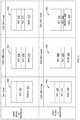
- FIG. 3illustrates cross-sectional views of semiconductor structures 350 , 352 , 354 , 356 , 358 , and 360 with layers deposited thereon after an annealing process is performed according to an embodiment of the disclosure.
- the results of the annealing process performed on the semiconductor structures 350 , 352 , 354 , 356 , 358 , and 360can be used to determine a thickness of the liner layer that provides sufficient protection against oxidation of the underlying Si-containing layer or SiGe layer during a subsequent annealing processes.
- the semiconductor structures 350 , 352 , and 354illustrate results of an annealing process conducted at a temperature of 400 degrees Celsius, a pressure of 30 bar, a processing time of 1 hour, and wet etching rate ratio (WERR) of less than 2.5.
- the semiconductor structure 350includes an SiO layer 302 and an SiGeOx layer 304 exposed to the annealing process described above. Prior to the annealing process, the SiO layer 302 has a thickness of about 2400 ⁇ and the SiGe layer has a thickness of about 1024 ⁇ . After the annealing process, the SiGe layer is converted to the SiGe oxidation (SiGeOx) layer 304 .
- the semiconductor structure 352includes an SiO layer 306 with a thickness of about 2230 ⁇ disposed on a silicon nitride (SiN) layer 308 with a thickness of about 100 ⁇ .
- the SiN layer 308is disposed on an SiGe layer 310 with a thickness of about 460 ⁇ . After the annealing process, a small portion of the SiN layer 308 is oxidized. However, the SiN layer 308 substantially reduces an amount of oxidation of the SiGe layer 310 compared to the SiGeOx layer 304 of the semiconductor structure 350 , such that substantially no oxidation of the SiGe layer 310 occurred.
- the semiconductor structure 354includes an SiO layer 312 with a thickness of about 2230 ⁇ disposed on an SiN layer 314 with a thickness of about 20 ⁇ .
- the SiN layeris disposed on an SiGe layer 316 with a thickness of about 460 ⁇ . After the annealing process, a small portion of the SiN layer 314 is oxidized. However, the SiN layer 314 substantially reduces an amount of oxidation of the SiGe layer 316 compared to the SiGeOx layer 304 of the semiconductor structure 350 , such that substantially no oxidation of the SiGe layer 316 occurred.
- Lack of oxidation of SiGe layer 310 on the semiconductor structure 352 and lack of oxidation of the of the SiGe layer 316 on the semiconductor structure 354indicate that a SiN layer with a thickness of about 20 ⁇ or greater substantially reduces oxidation of an underlying SiGe layer of the semiconductor structure with a SiO layer with a thickness of about 2200 ⁇ thickness during the annealing process described above.
- the semiconductor structures 356 , 358 , and 340illustrate results of an annealing process conducted at a temperature of 450 degrees Celsius, a pressure of 30 bar, a processing time of 1 hour, and WERR of less than 2.0.
- the semiconductor structure 356includes an SiO layer 320 with a thickness of about 2230 ⁇ disposed on a SiN layer 322 with a thickness of about 100 ⁇ .
- the SiN layer 322is disposed on an SiGe layer 324 with a thickness of about 479 ⁇ . After the annealing process, a small portion of the SiN layer 322 is oxidized. However, the SiGe layer 324 remains intact with substantially no oxidation.
- the semiconductor structure 358includes an SiO layer 326 with a thickness of about of 2400 ⁇ disposed on an SiN layer 328 with a thickness of about 30 ⁇ .
- the SiN layer 328is disposed on an SiGe layer 330 with a thickness of about 460 ⁇ . After the annealing process, the entire SiN layer 328 is oxidized. However, the SiGe layer 330 remains substantially intact with substantially no oxidation.
- the semiconductor structure 360includes an SiO layer 332 with a thickness of about 2190 ⁇ disposed on an SiN layer 334 with a thickness of about 20 ⁇ .
- the SiN layer 334is disposed on an SiGe layer with a thickness of about 620 ⁇ (prior to the annealing process). After the annealing process, most of the SiN layer 334 is oxidized. Further, a portion of the SiGe layer (i.e., SiGeOx layer 336 ) with a thickness of about 280 ⁇ is oxidized. A remaining portion of the SiGe layer 338 that is not oxidized has a thickness of about 340 ⁇ .
- FIG. 4is a schematic top view of a processing system 480 that can be used to perform the fabrication process illustrated in FIG. 1 according to an embodiment of the present disclosure.
- the cluster system 480is a modular system comprising multiple chambers (e.g., process chambers 490 A- 490 D, service chambers 491 A- 491 B, or the like) which perform various functions, including: substrate center-finding and orientation, degassing, annealing, deposition, etching, and the like.
- the process chambers 490 A- 490 D of the cluster system 480include a deposition chamber, an etch chamber, a plasma chamber, and an annealing chamber, configured to perform at least portions of the fabrication process 100 , and may further include chambers such as an ion implantation chamber and the like.
- the chambers 490 A- 490 Dinclude a processing chamber comprising a chamber wall forming a process volume therein, a substrate support for supporting a substrate within the process volume, a pressure regulator for regulating the pressure in the process volume, a gas inlet for providing gas to the process volume, and a gas outlet for exhausting gas from the process volume.
- the plasma chamberincludes at least one electrode to provide power to a plasma chamber enclosure for generating and sustaining a plasma therein.
- the plasma chamberalso includes at least one RF power source electrically connected to the at least one electrode.
- the etching chamberincludes an etching gas source to feed an etching gas into a processing chamber.
- the deposition chamberincludes precursor gas sources to introduce reactive gases into a processing chamber.
- the annealing chamberincludes an annealing gas source to introduce an annealing gas into a processing chamber.
- An ion implantation chambercomprises an arc chamber, filaments positioned within the arc chamber, and a repeller structure positioned between the filaments and the arc chamber.
- the duster system 480 for practicing embodiments of the present disclosureincludes a first deposition chamber configured to form a semiconductor structure on a substrate where the semiconductor structure includes a silicon (Si) containing layer or a silicon germanium (SiGe) layer.
- the cluster system 480also includes an etch chamber configured to etch a patterned semiconductor structure and a second deposition chamber configured to perform a liner deposition process to form a liner layer over the semiconductor structure.
- a third deposition chamber of the cluster system 480is configured to perform a flowable layer deposition process to form a flowable layer over the liner layer.
- An annealing chamber of the cluster system 480is configured to perform an annealing process by exposing the flowable layer to high pressure steam.
- the cluster system 480further includes a lithograph device to pattern the semiconductor structure using extreme ultraviolet light.
- the multiple chambers 490 A- 490 D of the cluster system 480are mounted to a central vacuum transfer chamber 488 which houses a robot 489 adapted to transfer substrates between the chambers 490 A- 490 D.
- the vacuum transfer chamber 488is maintained at a vacuum condition and provides an intermediate stage for transferring substrates from one chamber to another, and/or to a load lock chamber 484 positioned at a front end of the cluster system 480 .
- a front-end environment 483is positioned in selective communication with the load lock chambers 484 .
- a pod loader 485 disposed in the front-end environment 483is capable of linear and rotational movement (arrows 482 ) to transfer cassettes of substrates between the load lock chambers 484 and a plurality of pods 487 which are mounted on the front-end environment 483 .
- the cluster system 480also includes a controller 481 programmed to carry out the various processing methods performed in the cluster system 880 .
- the controller 481may be configured to control a flow of various precursor and process gases from gas sources and control processing parameters associated with material deposition or etching processes.
- the controller 481includes a programmable central processing unit (CPU) 479 that is operable with a memory 477 , and a mass storage device, an input control unit, and a display unit (not shown), such as power supplies, clocks, cache, input/output (I/O) circuits, and the like, coupled to the various components of the cluster system 480 to facilitate control of the substrate processing.
- the controller 481also includes hardware for monitoring substrate processing through sensors in the cluster system 480 . Other sensors that measure system parameters such as substrate temperature, chamber atmosphere pressure, and the like, may also provide information to the controller 481 .
- the CPU 479may be one of any form of general purpose computer processor that can be used in an industrial setting, such as a programmable logic controller (PLC), for controlling various chambers and sub-processors.
- the memory 477is coupled to the CPU 479 and the memory 477 is non-transitory and may be one or more of readily available memory such as random access memory (RAM), read only memory (ROM), floppy disk drive, hard disk, or any other form of digital storage, local or remote.
- Support circuits 475are coupled to the CPU 479 for supporting the processor in a conventional manner. Deposition, etching, annealing, and other processes are generally stored in the memory 477 , typically as a software routine. The software routine may also be stored and/or executed by a second CPU (not shown) that is remotely located from the hardware being controlled by the CPU 479 .
- the memory 477is in the form of computer-readable storage media that contains instructions, that when executed by the CPU 479 , facilitates the operation of the cluster system 480 .
- the instructions in the memory 477are in the form of a program product such as a program that implements the methods of the present disclosure.
- the program codemay conform to any one of a number of different programming languages.
- the disclosuremay be implemented as a program product stored on computer-readable storage media for use with a computer system.
- the program(s) of the program productinclude functions of the embodiments (including the methods described herein).
- Illustrative computer-readable storage mediainclude, but are not limited to: (i) non-writable storage media (e.g., read-only memory devices within a computer such as CD-ROM disks readable by a CD-ROM drive, flash memory, ROM chips or any type of solid-state non-volatile semiconductor memory) on which information is permanently stored; and (ii) writable storage media (e.g., a disk storage or a hard-disk drive or any type of solid-state random-access semiconductor memory) on which alterable information is stored.
- non-writable storage mediae.g., read-only memory devices within a computer such as CD-ROM disks readable by a CD-ROM drive, flash memory, ROM chips or any type of solid-state non-volatile semiconductor memory
- writable storage mediae.g., a disk storage or a hard-disk drive or any type of solid-state random-access semiconductor memory
Landscapes
- Engineering & Computer Science (AREA)
- Physics & Mathematics (AREA)
- Microelectronics & Electronic Packaging (AREA)
- Condensed Matter Physics & Semiconductors (AREA)
- General Physics & Mathematics (AREA)
- Manufacturing & Machinery (AREA)
- Computer Hardware Design (AREA)
- Power Engineering (AREA)
- Chemical & Material Sciences (AREA)
- Chemical Kinetics & Catalysis (AREA)
- Plasma & Fusion (AREA)
- Robotics (AREA)
- Formation Of Insulating Films (AREA)
- Insulated Gate Type Field-Effect Transistor (AREA)
- Element Separation (AREA)
Abstract
Description
Claims (20)
Priority Applications (1)
| Application Number | Priority Date | Filing Date | Title |
|---|---|---|---|
| US16/644,150US11177128B2 (en) | 2017-09-12 | 2018-09-11 | Apparatus and methods for manufacturing semiconductor structures using protective barrier layer |
Applications Claiming Priority (3)
| Application Number | Priority Date | Filing Date | Title |
|---|---|---|---|
| US201762557501P | 2017-09-12 | 2017-09-12 | |
| PCT/US2018/050464WO2019055415A1 (en) | 2017-09-12 | 2018-09-11 | Apparatus and methods for manufacturing semiconductor structures using protective barrier layer |
| US16/644,150US11177128B2 (en) | 2017-09-12 | 2018-09-11 | Apparatus and methods for manufacturing semiconductor structures using protective barrier layer |
Publications (2)
| Publication Number | Publication Date |
|---|---|
| US20200388486A1 US20200388486A1 (en) | 2020-12-10 |
| US11177128B2true US11177128B2 (en) | 2021-11-16 |
Family
ID=65724027
Family Applications (1)
| Application Number | Title | Priority Date | Filing Date |
|---|---|---|---|
| US16/644,150ActiveUS11177128B2 (en) | 2017-09-12 | 2018-09-11 | Apparatus and methods for manufacturing semiconductor structures using protective barrier layer |
Country Status (7)
| Country | Link |
|---|---|
| US (1) | US11177128B2 (en) |
| JP (1) | JP7274461B2 (en) |
| KR (1) | KR102659317B1 (en) |
| CN (1) | CN111095524B (en) |
| SG (1) | SG11202001450UA (en) |
| TW (1) | TWI697050B (en) |
| WO (1) | WO2019055415A1 (en) |
Families Citing this family (7)
| Publication number | Priority date | Publication date | Assignee | Title |
|---|---|---|---|---|
| US12142479B2 (en)* | 2020-01-17 | 2024-11-12 | Asm Ip Holding B.V. | Formation of SiOCN thin films |
| US12341005B2 (en) | 2020-01-17 | 2025-06-24 | Asm Ip Holding B.V. | Formation of SiCN thin films |
| CN111261634A (en)* | 2020-02-10 | 2020-06-09 | 无锡拍字节科技有限公司 | Manufacturing equipment and method of memory device |
| US11791155B2 (en) | 2020-08-27 | 2023-10-17 | Applied Materials, Inc. | Diffusion barriers for germanium |
| TWI749955B (en)* | 2020-09-28 | 2021-12-11 | 天虹科技股份有限公司 | Manufacturing method and manufacturing machine for reducing non-radiative recombination of micro led |
| KR20240041869A (en)* | 2021-08-23 | 2024-04-01 | 가부시키가이샤 코쿠사이 엘렉트릭 | Processing method, manufacturing method of semiconductor device, processing device and program |
| CN119170536A (en)* | 2024-11-21 | 2024-12-20 | 上海邦芯半导体科技有限公司 | Semiconductor processing machine |
Citations (351)
| Publication number | Priority date | Publication date | Assignee | Title |
|---|---|---|---|---|
| US3749383A (en) | 1971-04-29 | 1973-07-31 | Rca Corp | Apparatus for processing semiconductor devices |
| US3758316A (en) | 1971-03-30 | 1973-09-11 | Du Pont | Refractory materials and process for making same |
| US4524587A (en) | 1967-01-10 | 1985-06-25 | Kantor Frederick W | Rotary thermodynamic apparatus and method |
| US4576652A (en) | 1984-07-12 | 1986-03-18 | International Business Machines Corporation | Incoherent light annealing of gallium arsenide substrate |
| JPS634616A (en) | 1986-06-25 | 1988-01-09 | Hitachi Tokyo Electron Co Ltd | Steam treating unit |
| JPH01218018A (en) | 1988-02-18 | 1989-08-31 | Internatl Business Mach Corp <Ibm> | Method of converting semiconductor material into high melting point metal and semiconductor device manufactured by utilizing the method |
| US4879259A (en) | 1987-09-28 | 1989-11-07 | The Board Of Trustees Of The Leland Stanford Junion University | Rapid thermal annealing of gallium arsenide with trimethyl arsenic overpressure |
| US5050540A (en) | 1991-01-29 | 1991-09-24 | Arne Lindberg | Method of gas blanketing a boiler |
| US5114513A (en) | 1988-10-27 | 1992-05-19 | Omron Tateisi Electronics Co. | Optical device and manufacturing method thereof |
| US5126117A (en) | 1990-05-22 | 1992-06-30 | Custom Engineered Materials, Inc. | Device for preventing accidental releases of hazardous gases |
| US5149378A (en) | 1989-04-10 | 1992-09-22 | Hashimoto Kasei Kabushiki-Kaisya | Tungsten film forming apparatus |
| US5167717A (en) | 1989-02-15 | 1992-12-01 | Charles Boitnott | Apparatus and method for processing a semiconductor wafer |
| JPH04355922A (en) | 1991-03-18 | 1992-12-09 | Matsushita Electron Corp | Polyimide hardening device |
| US5175123A (en) | 1990-11-13 | 1992-12-29 | Motorola, Inc. | High-pressure polysilicon encapsulated localized oxidation of silicon |
| US5300320A (en) | 1992-06-23 | 1994-04-05 | President And Fellows Of Harvard College | Chemical vapor deposition from single organometallic precursors |
| US5314541A (en) | 1991-05-28 | 1994-05-24 | Tokyo Electron Limited | Reduced pressure processing system and reduced pressure processing method |
| US5319212A (en) | 1992-10-07 | 1994-06-07 | Genus, Inc. | Method of monitoring ion beam current in ion implantation apparatus for use in manufacturing semiconductors |
| JPH06283496A (en) | 1993-03-26 | 1994-10-07 | Dainippon Screen Mfg Co Ltd | Dryer of substrate after washing |
| US5366905A (en) | 1991-11-05 | 1994-11-22 | Fujitsu Limited | Method for producing conducting layers for a semiconductor device |
| JPH0748489B2 (en) | 1987-07-27 | 1995-05-24 | 富士通株式会社 | Plasma processing device |
| US5472812A (en) | 1991-07-11 | 1995-12-05 | Canon Kabushiki Kaisha | Method for forming a photomask pattern |
| JPH08195493A (en) | 1995-01-13 | 1996-07-30 | Toshiba Corp | Method for manufacturing thin film transistor |
| US5578132A (en) | 1993-07-07 | 1996-11-26 | Tokyo Electron Kabushiki Kaisha | Apparatus for heat treating semiconductors at normal pressure and low pressure |
| US5590695A (en) | 1993-04-28 | 1997-01-07 | Advanced Delivery & Chemical Systems, Inc. | Manifold systems for high purity chemical delivery systems |
| US5597439A (en) | 1994-10-26 | 1997-01-28 | Applied Materials, Inc. | Process gas inlet and distribution passages |
| US5620524A (en) | 1995-02-27 | 1997-04-15 | Fan; Chiko | Apparatus for fluid delivery in chemical vapor deposition systems |
| US5677230A (en) | 1995-12-01 | 1997-10-14 | Motorola | Method of making wide bandgap semiconductor devices |
| JPH09296267A (en) | 1995-11-21 | 1997-11-18 | Applied Materials Inc | Apparatus and method for manufacturing metal path in semiconductor substrate by high-pressure extrusion |
| JPH10214880A (en) | 1996-12-02 | 1998-08-11 | Applied Materials Inc | Substrate support member |
| US5808245A (en) | 1995-01-03 | 1998-09-15 | Donaldson Company, Inc. | Vertical mount catalytic converter muffler |
| JPH10335657A (en) | 1997-06-04 | 1998-12-18 | Nec Corp | Manufacture of semiconductor device |
| US5858051A (en) | 1995-05-08 | 1999-01-12 | Toshiba Machine Co., Ltd. | Method of manufacturing optical waveguide |
| US5857368A (en) | 1995-10-06 | 1999-01-12 | Applied Materials, Inc. | Apparatus and method for fabricating metal paths in semiconductor substrates through high pressure extrusion |
| US5880041A (en) | 1994-05-27 | 1999-03-09 | Motorola Inc. | Method for forming a dielectric layer using high pressure |
| US5879756A (en) | 1996-09-19 | 1999-03-09 | Lambda Technologies, Inc. | Curing polymer layers on semiconductor substrates using variable frequency microwave energy |
| US5940985A (en) | 1996-03-01 | 1999-08-24 | Tokyo Electron Limited | Apparatus and method for drying substrates |
| JPH11354515A (en) | 1998-06-04 | 1999-12-24 | Ishikawajima Harima Heavy Ind Co Ltd | Pressurized heating furnace |
| US6082950A (en) | 1996-11-18 | 2000-07-04 | Applied Materials, Inc. | Front end wafer staging with wafer cassette turntables and on-the-fly wafer center finding |
| US6136664A (en) | 1997-08-07 | 2000-10-24 | International Business Machines Corporation | Filling of high aspect ratio trench isolation |
| US6150286A (en) | 2000-01-03 | 2000-11-21 | Advanced Micro Devices, Inc. | Method of making an ultra thin silicon nitride film |
| US6164412A (en) | 1998-04-03 | 2000-12-26 | Arvin Industries, Inc. | Muffler |
| JP2001110729A (en) | 1999-10-06 | 2001-04-20 | Mitsubishi Heavy Ind Ltd | Apparratus for continuously manufacturing method of semiconductor element |
| US6242368B1 (en) | 1996-03-29 | 2001-06-05 | Praxair Technology, Inc. | Removal of carbon from substrate surface |
| EP1107288A2 (en) | 1999-11-30 | 2001-06-13 | Applied Materials, Inc. | Substrate processing system and method |
| US6251751B1 (en) | 1997-10-16 | 2001-06-26 | International Business Machines Corporation | Bulk and strained silicon on insulator using local selective oxidation |
| US6299753B1 (en) | 1999-09-01 | 2001-10-09 | Applied Materials, Inc. | Double pressure vessel chemical dispenser unit |
| US20010029108A1 (en) | 2000-03-06 | 2001-10-11 | Kouji Tometsuka | Substrate processeing apparatus, substrate processing method and electronic device manufacturing method |
| US20010041122A1 (en) | 1998-09-28 | 2001-11-15 | Applied Materials, Inc. | Single wafer load lock with internal wafer transport |
| US6319766B1 (en) | 2000-02-22 | 2001-11-20 | Applied Materials, Inc. | Method of tantalum nitride deposition by tantalum oxide densification |
| US20010050096A1 (en) | 2000-04-18 | 2001-12-13 | Costantini Michael A. | Supercritical fluid delivery and recovery system for semiconductor wafer processing |
| US6334266B1 (en) | 1999-09-20 | 2002-01-01 | S.C. Fluids, Inc. | Supercritical fluid drying system and method of use |
| US6368412B1 (en) | 1997-11-18 | 2002-04-09 | Nec Corporation | Apparatus with high temperature gas releasing means for vapor deposition of parylene polymer without peeling |
| US6387764B1 (en) | 1999-04-02 | 2002-05-14 | Silicon Valley Group, Thermal Systems Llc | Trench isolation process to deposit a trench fill oxide prior to sidewall liner oxidation growth |
| US20020066535A1 (en) | 1995-07-10 | 2002-06-06 | William Brown | Exhaust system for treating process gas effluent |
| US20020073922A1 (en) | 1996-11-13 | 2002-06-20 | Jonathan Frankel | Chamber liner for high temperature processing chamber |
| US6442980B2 (en) | 1997-11-26 | 2002-09-03 | Chart Inc. | Carbon dioxide dry cleaning system |
| US20020122885A1 (en) | 2001-03-01 | 2002-09-05 | Micron Technology, Inc. | Methods, systems, and apparatus for uniform chemical-vapor depositions |
| US20020134439A1 (en) | 2001-03-22 | 2002-09-26 | Hiroyuki Kawasaki | Gas recirculation flow control method and apparatus for use in vacuum system |
| US20020151128A1 (en) | 1996-01-22 | 2002-10-17 | Lane Richard H. | High-pressure anneal process for integrated circuits |
| US20020148492A1 (en) | 2001-04-17 | 2002-10-17 | Kabushiki Kaisha Kobe Seiko Sho | High-pressure processing apparatus |
| US6468490B1 (en) | 2000-06-29 | 2002-10-22 | Applied Materials, Inc. | Abatement of fluorine gas from effluent |
| US20020155714A1 (en) | 2001-04-20 | 2002-10-24 | Kawasaki Microelectronics, Inc. Mihama-Ku, Japan | Method of conditioning an etching chamber and method of processing semiconductor substrate using the etching chamber |
| US20020192056A1 (en) | 2001-06-13 | 2002-12-19 | Applied Materials, Inc. | Method and apparatus for transferring a semiconductor substrate |
| US6500603B1 (en) | 1999-11-11 | 2002-12-31 | Mitsui Chemicals, Inc. | Method for manufacturing polymer optical waveguide |
| US20030022487A1 (en) | 2001-07-25 | 2003-01-30 | Applied Materials, Inc. | Barrier formation using novel sputter-deposition method |
| US20030030945A1 (en) | 2001-08-10 | 2003-02-13 | Seagate Technology Llc | Tunneling magnetoresistive sensor with spin polarized current injection |
| JP2003051474A (en) | 2001-08-03 | 2003-02-21 | Kobe Steel Ltd | High-pressure processing apparatus |
| US20030049372A1 (en) | 1997-08-11 | 2003-03-13 | Cook Robert C. | High rate deposition at low pressures in a small batch reactor |
| US20030053893A1 (en) | 2001-08-31 | 2003-03-20 | Hitachi Kokusai Electric Inc. | Substrate processing apparatus and a method for fabricating a semiconductor device by using same |
| US20030101938A1 (en) | 1998-10-27 | 2003-06-05 | Applied Materials, Inc. | Apparatus for the deposition of high dielectric constant films |
| JP2003166065A (en) | 2001-11-30 | 2003-06-13 | Sekisui Chem Co Ltd | Discharge plasma treatment apparatus |
| US6583497B2 (en) | 1999-08-17 | 2003-06-24 | Applied Materials Inc. | Surface treatment of c-doped SiO2 film to enhance film stability during O2 ashing |
| KR20030052162A (en) | 2001-12-20 | 2003-06-26 | 동부전자 주식회사 | Post treatment method for metal line of semiconductor device |
| US20030121887A1 (en) | 2001-03-22 | 2003-07-03 | Garvey James F. | Multi-component substances and processes for preparation thereof |
| JP2003188387A (en) | 2001-12-20 | 2003-07-04 | Sony Corp | Thin film transistor and its fabricating method |
| US20030148035A1 (en) | 2002-02-07 | 2003-08-07 | Applied Materials, Inc. | Article for use in a semiconductor processing chamber and method of fabricating same |
| US20030148631A1 (en) | 1999-11-08 | 2003-08-07 | Taiwan Semiconductor Manufacturing Company | Oxidative annealing method for forming etched spin-on-glass (SOG) planarizing layer with uniform etch profile |
| US6619304B2 (en) | 2001-09-13 | 2003-09-16 | Micell Technologies, Inc. | Pressure chamber assembly including non-mechanical drive means |
| US20030194615A1 (en) | 2002-04-12 | 2003-10-16 | Krauth Anthony C. | Use of a planarizing layer to improve multilayer performance in extreme ultra-violet masks |
| US20030207593A1 (en) | 2002-05-02 | 2003-11-06 | Micron Technology, Inc. | Atomic layer deposition and conversion |
| US20030232512A1 (en) | 2002-06-13 | 2003-12-18 | Dickinson C. John | Substrate processing apparatus and related systems and methods |
| US20040025908A1 (en) | 2000-04-18 | 2004-02-12 | Stephen Douglas | Supercritical fluid delivery system for semiconductor wafer processing |
| US20040060519A1 (en) | 2002-10-01 | 2004-04-01 | Seh America Inc. | Quartz to quartz seal using expanded PTFE gasket material |
| US20040074869A1 (en) | 2002-10-18 | 2004-04-22 | Applied Materials, Inc. | Fluorine free integrated process for etching aluminum including chamber dry clean |
| JP2004127958A (en) | 2002-09-30 | 2004-04-22 | Kyoshin Engineering:Kk | Apparatus and method for performing high pressure anneal steam treatment |
| US20040112409A1 (en) | 2002-12-16 | 2004-06-17 | Supercritical Sysems, Inc. | Fluoride in supercritical fluid for photoresist and residue removal |
| US20040184792A1 (en) | 2003-03-17 | 2004-09-23 | Tokyo Electron Limited | Processing system and method for thermally treating a substrate |
| US20040219800A1 (en) | 2001-06-22 | 2004-11-04 | Marcel Tognetti | Thermal oxidation process control by controlling oxidation agent partial pressure |
| WO2004102055A1 (en) | 2003-05-13 | 2004-11-25 | Applied Materials, Inc. | Methods and apparatus for sealing an opening of a processing chamber |
| US20040248392A1 (en) | 2003-02-04 | 2004-12-09 | Applied Materials, Inc. | Tailoring nitrogen profile in silicon oxynitride using rapid thermal annealing with ammonia under ultra-low pressure |
| US20040255979A1 (en) | 2003-06-18 | 2004-12-23 | Fury Michael A. | Load lock system for supercritical fluid cleaning |
| US20050003655A1 (en) | 1998-02-27 | 2005-01-06 | Micron Technology, Inc. | MOCVD process using ozone as a reactant to deposit a metal oxide barrier layer |
| US6841432B1 (en) | 1993-08-20 | 2005-01-11 | Semiconductor Energy Laboratory Co., Ltd. | Semiconductor device and process for fabricating the same |
| JP2005064269A (en) | 2003-08-13 | 2005-03-10 | Kobe Steel Ltd | High pressure processing method |
| JP2005079528A (en) | 2003-09-03 | 2005-03-24 | Kyoshin Engineering:Kk | High precision high pressure annealer |
| US20050082281A1 (en) | 2002-11-25 | 2005-04-21 | Susumu Uemori | Electric heater for a semiconductor processing apparatus |
| US6906761B2 (en) | 2001-09-19 | 2005-06-14 | Keiwa Inc. | Reflection sheet and backlight unit using the same |
| US20050136684A1 (en) | 2003-12-23 | 2005-06-23 | Applied Materials, Inc. | Gap-fill techniques |
| WO2005057663A2 (en) | 2003-12-10 | 2005-06-23 | Koninklijke Philips Electronics N.V. | Method and apparatus for fabrication of metal-oxide semiconductor integrated circuit devices |
| US20050161158A1 (en) | 2003-12-23 | 2005-07-28 | Schumacher John C. | Exhaust conditioning system for semiconductor reactor |
| US20050191828A1 (en) | 2000-08-11 | 2005-09-01 | Applied Materials, Inc. | Method for ion implanting insulator material to reduce dielectric constant |
| TW200529284A (en) | 2004-02-19 | 2005-09-01 | Taiwan Semiconductor Mfg | An intelligent full automation controlled flow for a semiconductor furnace tool |
| US20050198971A1 (en) | 2002-10-02 | 2005-09-15 | Kelly Leitch | High pressure CO2 purification and supply system |
| US20050250347A1 (en) | 2003-12-31 | 2005-11-10 | Bailey Christopher M | Method and apparatus for maintaining by-product volatility in deposition process |
| JP2005333015A (en) | 2004-05-20 | 2005-12-02 | Kobe Steel Ltd | Method for desiccating microstructure, and microstructure obtained thereby |
| US20050269291A1 (en) | 2004-06-04 | 2005-12-08 | Tokyo Electron Limited | Method of operating a processing system for treating a substrate |
| US20060003596A1 (en) | 2004-07-01 | 2006-01-05 | Micron Technology, Inc. | Low temperature process for polysilazane oxidation/densification |
| US20060035035A1 (en) | 1997-05-10 | 2006-02-16 | Semiconductor Energy Laboratory Co., Ltd. | Film forming method and film forming apparatus |
| US20060105107A1 (en) | 2004-10-15 | 2006-05-18 | Lindeboom Bartholomeus H L | Reactor design for reduced particulate generation |
| US20060124613A1 (en) | 2002-05-08 | 2006-06-15 | Satyendra Kumar | Plasma-assisted heat treatment |
| US7084079B2 (en) | 2001-08-10 | 2006-08-01 | International Business Machines Corporation | Method for low temperature chemical vapor deposition of low-k films using selected cyclosiloxane and ozone gases for semiconductor applications |
| US20060175012A1 (en) | 2005-02-07 | 2006-08-10 | Beung-Keun Lee | Semiconductor fabrication equipment and method for controlling pressure |
| US7105061B1 (en) | 2001-11-07 | 2006-09-12 | Novellus Systems, Inc. | Method and apparatus for sealing substrate load port in a high pressure reactor |
| US20060207633A1 (en) | 2005-03-21 | 2006-09-21 | Pkl Co., Ltd. | Device and method for cleaning photomask |
| US7111630B2 (en) | 2001-05-17 | 2006-09-26 | Dainippon Screen Mfg. Co., Ltd. | High pressure processing apparatus and method |
| US7114517B2 (en) | 2001-11-26 | 2006-10-03 | Sund Wesley E | High purity fluid delivery system |
| US20060226117A1 (en) | 2005-03-29 | 2006-10-12 | Bertram Ronald T | Phase change based heating element system and method |
| US20060279025A1 (en) | 2005-06-10 | 2006-12-14 | Babak Heidari | Pattern replication with intermediate stamp |
| US20060290017A1 (en) | 2005-06-28 | 2006-12-28 | Masaki Yanagisawa | Method for transcribing patterns on resin body, method for manufacturing planar waveguide, and method for manufacturing micro-lens |
| US20070012402A1 (en) | 2003-07-08 | 2007-01-18 | Sundew Technologies, Llc | Apparatus and method for downstream pressure control and sub-atmospheric reactive gas abatement |
| US20070045753A1 (en) | 2005-08-30 | 2007-03-01 | Sangwoo Pae | Semiconductor device having a metal gate electrode formed on an annealed high-k gate dielectric layer |
| US20070087533A1 (en) | 2005-10-19 | 2007-04-19 | Moore Epitaxial Inc. | Gas ring and method of processing substrates |
| US7211525B1 (en) | 2005-03-16 | 2007-05-01 | Novellus Systems, Inc. | Hydrogen treatment enhanced gap fill |
| TW200721316A (en) | 2005-08-05 | 2007-06-01 | Hitachi Int Electric Inc | Substrate processing apparatus, cooling gas feed nozzle and method for manufacturing semiconductor device |
| KR20070075383A (en) | 2003-03-07 | 2007-07-18 | 동경 엘렉트론 주식회사 | Tungsten Film Formation Method |
| US20070187386A1 (en) | 2006-02-10 | 2007-08-16 | Poongsan Microtec Corporation | Methods and apparatuses for high pressure gas annealing |
| US20070204797A1 (en) | 2006-03-03 | 2007-09-06 | Andreas Fischer | Methods and apparatus for selective pre-coating of a plasma processing chamber |
| US20070212850A1 (en) | 2002-09-19 | 2007-09-13 | Applied Materials, Inc. | Gap-fill depositions in the formation of silicon containing dielectric materials |
| JP2007242791A (en) | 2006-03-07 | 2007-09-20 | Hitachi Kokusai Electric Inc | Substrate processing equipment |
| US7282458B2 (en) | 2004-01-16 | 2007-10-16 | International Business Machines Corporation | Low K and ultra low K SiCOH dielectric films and methods to form the same |
| US20070243317A1 (en) | 2002-07-15 | 2007-10-18 | Du Bois Dale R | Thermal Processing System and Configurable Vertical Chamber |
| US20070256559A1 (en) | 2006-05-08 | 2007-11-08 | The Board Of Trustees Of The University Of Illinois | Integrated vacuum absorption steam cycle gas separation |
| US20080074658A1 (en) | 2003-12-23 | 2008-03-27 | Davis Matthew F | Method and apparatus for performing limited area spectral analysis |
| JP2008073611A (en) | 2006-09-21 | 2008-04-03 | Dainippon Screen Mfg Co Ltd | High pressure treating device |
| US20080083109A1 (en) | 2006-09-25 | 2008-04-10 | Hitachi Kokusai Electric Inc. | Substrate processing apparatus and attaching/detaching method of reaction vessel |
| US7361231B2 (en) | 2005-07-01 | 2008-04-22 | Ekc Technology, Inc. | System and method for mid-pressure dense phase gas and ultrasonic cleaning |
| WO2008047886A1 (en) | 2006-10-13 | 2008-04-24 | Asahi Glass Co., Ltd. | Method of smoothing surface of substrate for euv mask blank, and euv mask blank obtained by the method |
| US20080115726A1 (en) | 2004-08-27 | 2008-05-22 | Applied Materials, Inc. | gap-fill depositions introducing hydroxyl-containing precursors in the formation of silicon containing dielectric materials |
| US20080121882A1 (en) | 2006-11-07 | 2008-05-29 | Jack Hwang | Method to reduce junction leakage through partial regrowth with ultrafast anneal and structures formed thereby |
| JP2008153635A (en) | 2006-11-22 | 2008-07-03 | Toshiba Matsushita Display Technology Co Ltd | Manufacturing method of mos type semiconductor device |
| WO2008089178A2 (en) | 2007-01-16 | 2008-07-24 | Varian Semiconductor Equipment Associates, Inc. | Plasma source with liner for reducing metal contamination |
| US20080210273A1 (en) | 2005-11-08 | 2008-09-04 | Tokyo Electron Limited | Batch photoresist dry strip and ash system and process |
| US20080241384A1 (en) | 2007-04-02 | 2008-10-02 | Asm Genitech Korea Ltd. | Lateral flow deposition apparatus and method of depositing film by using the apparatus |
| US20080251904A1 (en) | 2007-04-13 | 2008-10-16 | Infineon Technologies Ag | Curing layers of a semiconductor product using electromagnetic fields |
| US20080268635A1 (en) | 2001-07-25 | 2008-10-30 | Sang-Ho Yu | Process for forming cobalt and cobalt silicide materials in copper contact applications |
| US7460760B2 (en) | 2005-09-13 | 2008-12-02 | Electronics And Telecommunications Research Institute | Optical waveguide master and method of manufacturing the same |
| US20080315762A1 (en) | 2007-04-30 | 2008-12-25 | Ifire Ip Corporation | Laminated thick film dielectric structure for thick film dielectric electroluminescent displays |
| US20090018688A1 (en) | 2007-06-15 | 2009-01-15 | Applied Materials, Inc. | Methods and systems for designing and validating operation of abatement systems |
| KR20090011463A (en) | 2007-07-26 | 2009-02-02 | 주식회사 풍산마이크로텍 | Method of manufacturing semiconductor device through high pressure oxygen heat treatment |
| US7491658B2 (en) | 2004-10-13 | 2009-02-17 | International Business Machines Corporation | Ultra low k plasma enhanced chemical vapor deposition processes using a single bifunctional precursor containing both a SiCOH matrix functionality and organic porogen functionality |
| US7503334B1 (en) | 2002-02-05 | 2009-03-17 | Novellus Systems, Inc. | Apparatus and methods for processing semiconductor substrates using supercritical fluids |
| US20090081884A1 (en) | 2007-09-24 | 2009-03-26 | Yoshitaka Yokota | Method of improving oxide growth rate of selective oxidation processes |
| US7521089B2 (en) | 2002-06-13 | 2009-04-21 | Tokyo Electron Limited | Method and apparatus for controlling the movement of CVD reaction byproduct gases to adjacent process chambers |
| KR20090040867A (en) | 2007-10-22 | 2009-04-27 | 어플라이드 머티어리얼스, 인코포레이티드 | How to Form a Dielectric Layer in a Trench |
| US20090110622A1 (en) | 2007-10-26 | 2009-04-30 | Applied Materials, Inc. | Methods and apparatus for smart abatement using an improved fuel circuit |
| US7541297B2 (en) | 2007-10-22 | 2009-06-02 | Applied Materials, Inc. | Method and system for improving dielectric film quality for void free gap fill |
| JP2009129927A (en) | 2007-11-19 | 2009-06-11 | Jgc Catalysts & Chemicals Ltd | Method of repairing damaged low-dielectric constant silica-based film and low-dielectric-constant silica-based film restored by the same |
| KR20090064279A (en) | 2007-12-14 | 2009-06-18 | 노벨러스 시스템즈, 인코포레이티드 | Protective layer for damage-free gap filling |
| US20090180847A1 (en) | 2005-08-26 | 2009-07-16 | George Xinsheng Guo | Multi-chamber vacuum processing and transfer system |
| US20090186481A1 (en) | 2008-01-22 | 2009-07-23 | Tokyo Electron Limited | Method for integrating selective low-temperature ruthenium deposition into copper metallization of a semiconductor device |
| US7576441B2 (en) | 2003-06-17 | 2009-08-18 | Micron Technology, Inc. | Boron-doped amorphous carbon film for use as a hard etch mask during the formation of a semiconductor device |
| US20090233449A1 (en) | 2005-02-22 | 2009-09-17 | Xactix, Inc. | Etching chamber with subchamber |
| US20090243126A1 (en) | 2008-03-31 | 2009-10-01 | Ryuta Washiya | Method and apparatus for imprinting microstructure and stamper therefor |
| US20100006211A1 (en) | 2007-03-22 | 2010-01-14 | 3M Innovative Properties Company | Microreplication tools and patterns using laser induced thermal embossing |
| US20100012292A1 (en) | 2007-03-31 | 2010-01-21 | Tokyo Electron Limited | Trap apparatus, exhaust system and processing system using same |
| US7651959B2 (en) | 2007-12-03 | 2010-01-26 | Asm Japan K.K. | Method for forming silazane-based dielectric film |
| US7650965B2 (en) | 2006-06-09 | 2010-01-26 | Emcon Technologies Llc | Exhaust system |
| US20100022068A1 (en) | 2008-07-25 | 2010-01-28 | Neng-Kuo Chen | Sti film property using sod post-treatment |
| US20100072569A1 (en) | 2008-09-25 | 2010-03-25 | Samsung Electronics, Co., Ltd. | Method of forming an isolation layer, method of manufacturing a semiconductor device using the same, and semiconductor device having an isolation layer |
| US20100173495A1 (en) | 2004-11-22 | 2010-07-08 | Applied Materials, Inc. | Substrate processing apparatus using a batch processing chamber |
| US20100173470A1 (en) | 2009-01-08 | 2010-07-08 | Samsung Electronics Co., Ltd. | Methods of forming a silicon oxide layer and methods of forming an isolation layer |
| US20100196626A1 (en) | 2009-02-04 | 2010-08-05 | Applied Materials, Inc. | Ground return for plasma processes |
| US20100203725A1 (en) | 2009-02-12 | 2010-08-12 | Suk-Hun Choi | Methods of fabricating semiconductor devices and semiconductor devices including a contact plug processed by rapid thermal annealing |
| JP2010205854A (en) | 2009-03-02 | 2010-09-16 | Fujitsu Semiconductor Ltd | Method of manufacturing semiconductor device |
| CN101871043A (en) | 2010-06-25 | 2010-10-27 | 东莞市康汇聚线材科技有限公司 | Annealing furnace steam generator and control method thereof |
| US7825038B2 (en) | 2006-05-30 | 2010-11-02 | Applied Materials, Inc. | Chemical vapor deposition of high quality flow-like silicon dioxide using a silicon containing precursor and atomic oxygen |
| US7825042B2 (en) | 2000-01-18 | 2010-11-02 | Applied Materials, Inc. | Very low dielectric constant plasma-enhanced CVD films |
| US20100304027A1 (en) | 2009-05-27 | 2010-12-02 | Applied Materials, Inc. | Substrate processing system and methods thereof |
| US20100320459A1 (en) | 2009-06-22 | 2010-12-23 | Fujifilm Corporation | Thin film transistor and method of producing thin film transistor |
| US20100327422A1 (en) | 2009-06-29 | 2010-12-30 | Samsung Electronics Co., Ltd | Semiconductor chip, method of fabricating the same, and stack module and memory card including the same |
| US7867923B2 (en) | 2007-10-22 | 2011-01-11 | Applied Materials, Inc. | High quality silicon oxide films by remote plasma CVD from disilane precursors |
| JP2011029394A (en) | 2009-07-24 | 2011-02-10 | Utec:Kk | Pzt film, electronic component, method of manufacturing oxide material film, and steam pressure rapid heating device |
| US7891228B2 (en) | 2008-11-18 | 2011-02-22 | Mks Instruments, Inc. | Dual-mode mass flow verification and mass flow delivery system and method |
| US20110151677A1 (en) | 2009-12-21 | 2011-06-23 | Applied Materials, Inc. | Wet oxidation process performed on a dielectric material formed from a flowable cvd process |
| US20110165781A1 (en) | 2010-01-06 | 2011-07-07 | Applied Materials, Inc. | Flowable dielectric using oxide liner |
| US20110198736A1 (en) | 2010-02-17 | 2011-08-18 | Asm America, Inc. | Reactive site deactivation against vapor deposition |
| US8027089B2 (en) | 2005-10-07 | 2011-09-27 | Nikon Corporation | Minute structure and its manufacturing method |
| US20110263091A1 (en) | 2010-04-23 | 2011-10-27 | Semiconductor Energy Laboratory Co., Ltd. | Manufacturing method of semiconductor device |
| US20110303147A1 (en) | 2009-03-10 | 2011-12-15 | Mitsui Engineering & Shipbuilding Co., Ltd. | Atomic layer deposition apparatus |
| US20110305836A1 (en) | 2009-03-10 | 2011-12-15 | Mitsui Engineering & Shipbuilding Co., Ltd. | Atomic layer deposition apparatus and thin film forming method |
| KR20110136532A (en) | 2010-06-15 | 2011-12-21 | 서울대학교산학협력단 | 1T DRAM device having two gates in the recessed body, its operation method and manufacturing method |
| JP2012503883A (en) | 2008-09-24 | 2012-02-09 | ラム リサーチ コーポレーション | Method and system for preventing feature collapse during microelectronic topography manufacturing |
| US20120048304A1 (en) | 2010-08-30 | 2012-03-01 | Yukiko Kitajima | Supercritical drying method and supercritical drying system |
| US20120056173A1 (en) | 2010-09-03 | 2012-03-08 | Applied Materials, Inc. | Staggered thin film transistor and method of forming the same |
| US20120060868A1 (en) | 2005-06-07 | 2012-03-15 | Donald Gray | Microscale fluid delivery system |
| US20120112224A1 (en) | 2009-04-02 | 2012-05-10 | Saint-Gobain Glass France | Method for producing a structure with a textured external surface, intended for an organic light emitting diode device, and a structure with a textured external surface |
| US20120142192A1 (en) | 2010-07-30 | 2012-06-07 | Applied Materials, Inc. | Oxide-rich liner layer for flowable cvd gapfill |
| US20120175822A1 (en) | 2009-09-16 | 2012-07-12 | Bridgestone Corporation | Photo-curable transfer sheet and method for forming concave-convex pattern using the same |
| WO2012133583A1 (en) | 2011-03-30 | 2012-10-04 | 大日本印刷株式会社 | Supercritical drying device and supercritical drying method |
| US20120252210A1 (en) | 2011-03-30 | 2012-10-04 | Tokyo Electron Limited | Method for modifying metal cap layers in semiconductor devices |
| JP2012204656A (en) | 2011-03-25 | 2012-10-22 | Toshiba Corp | Supercritical drying method of semiconductor substrate |
| US8306026B2 (en) | 2005-12-15 | 2012-11-06 | Toshiba America Research, Inc. | Last hop topology sensitive multicasting key management |
| US20120285492A1 (en) | 2011-05-12 | 2012-11-15 | Applied Materials, Inc. | Methods of dry stripping boron-carbon films |
| US20120304485A1 (en) | 2011-05-30 | 2012-12-06 | Tokyo Electron Limited | Substrate processing method, substrate processing apparatus, and storage medium |
| US8349085B2 (en) | 2007-01-31 | 2013-01-08 | Tokyo Electron Limited | Substrate processing apparatus |
| JP2013516788A (en) | 2010-01-07 | 2013-05-13 | アプライド マテリアルズ インコーポレイテッド | In situ ozone curing for radical component CVD |
| US8449942B2 (en) | 2009-11-12 | 2013-05-28 | Applied Materials, Inc. | Methods of curing non-carbon flowable CVD films |
| JP2013105777A (en) | 2011-11-10 | 2013-05-30 | Tokyo Electron Ltd | Substrate processing apparatus, substrate processing method and storage medium |
| US8455368B2 (en) | 2007-05-25 | 2013-06-04 | Applied Materials, Inc. | Methods and apparatus for assembling and operating electronic device manufacturing systems |
| US8466073B2 (en) | 2011-06-03 | 2013-06-18 | Applied Materials, Inc. | Capping layer for reduced outgassing |
| KR101287035B1 (en) | 2013-05-07 | 2013-07-17 | 호용종합건설주식회사 | Boiler system for pipe regeneration |
| US20130194350A1 (en) | 2012-01-31 | 2013-08-01 | Ricoh Company, Ltd. | Thin film forming apparatus, thin film forming method, electro-mechanical transducer element, liquid ejecting head, and inkjet recording apparatus |
| JP2013179244A (en) | 2011-05-30 | 2013-09-09 | Toshiba Corp | Method for processing substrate, device for processing substrate and storage medium |
| KR101305904B1 (en) | 2011-12-07 | 2013-09-09 | 주식회사 테스 | Method of manufacturing a semiconductor device with minute pattern |
| US20130233170A1 (en) | 2005-09-13 | 2013-09-12 | Rasirc | Methods and devices for producing high purity steam |
| US8536065B2 (en) | 2010-10-05 | 2013-09-17 | Applied Materials, Inc. | Ultra high selectivity doped amorphous carbon strippable hardmask development and integration |
| US20130241037A1 (en) | 2009-03-18 | 2013-09-19 | Samsung Electronics Co., Ltd. | Semiconductor Devices Having Metal Oxide Patterns |
| US8557712B1 (en) | 2008-12-15 | 2013-10-15 | Novellus Systems, Inc. | PECVD flowable dielectric gap fill |
| US8563445B2 (en) | 2010-03-05 | 2013-10-22 | Applied Materials, Inc. | Conformal layers by radical-component CVD |
| US20130288485A1 (en) | 2012-04-30 | 2013-10-31 | Applied Materials, Inc. | Densification for flowable films |
| US20130330042A1 (en) | 2011-12-09 | 2013-12-12 | Furukawa Electric Co., Ltd. | Optical branching element and optical branching circuit |
| US20130337171A1 (en) | 2012-06-13 | 2013-12-19 | Qualcomm Mems Technologies, Inc. | N2 purged o-ring for chamber in chamber ald system |
| US20140003892A1 (en) | 2011-03-18 | 2014-01-02 | Tokyo Electron Limited | Gate valve unit, substrate processing device and substrate processing method thereof |
| KR20140003776A (en) | 2012-06-28 | 2014-01-10 | 주식회사 메카로닉스 | Preparation of a high resistivity zno thin film |
| US20140023320A1 (en) | 2011-03-25 | 2014-01-23 | Seo Young Lee | Lightwave Circuit and Method for Manufacturing Same |
| JP2014019912A (en) | 2012-07-19 | 2014-02-03 | Tokyo Electron Ltd | Method of depositing tungsten film |
| US20140045300A1 (en) | 2012-08-10 | 2014-02-13 | Taiwan Semiconductor Manufacturing Co., Ltd. | Warpage control in a package-on-package structure |
| US20140051264A1 (en) | 2012-03-05 | 2014-02-20 | Applied Materials, Inc. | Flowable films using alternative silicon precursors |
| US20140076494A1 (en) | 2012-09-18 | 2014-03-20 | Tokyo Electron Limited | Processing system |
| US20140134827A1 (en) | 2010-04-15 | 2014-05-15 | Novellus Systems, Inc. | Conformal film deposition for gapfill |
| US20140138802A1 (en) | 2011-06-16 | 2014-05-22 | Fujifilm Manufacturing Europe Bv | Method and Device for Manufacturing a Barrier Layer on a Flexible Substrate |
| US8741788B2 (en) | 2009-08-06 | 2014-06-03 | Applied Materials, Inc. | Formation of silicon oxide using non-carbon flowable CVD processes |
| US20140159135A1 (en) | 2012-12-12 | 2014-06-12 | Sandisk Technologies Inc. | Air Gap Isolation In Non-Volatile Memory Using Sacrificial Films |
| US20140183743A1 (en) | 2012-12-27 | 2014-07-03 | Tokyo Electron Limited | Manganese metal film forming method, processing system, electronic device manufacturing method and electronic device |
| US20140231384A1 (en) | 2013-02-19 | 2014-08-21 | Applied Materials, Inc. | Hdd patterning using flowable cvd film |
| US20140234583A1 (en) | 2011-07-14 | 2014-08-21 | Ltc Co., Ltd | Inorganic particle scattering film having a good light-extraction performance |
| US20140235068A1 (en) | 2011-11-01 | 2014-08-21 | Hitachi Kokusai Electric Inc. | Method of manufacturing semiconductor device, apparatus for manufacturing semiconductor device, and non-transitory computer-readable recording medium |
| US20140239291A1 (en) | 2013-02-27 | 2014-08-28 | Inha-Industry Partnership Institute | Metal-oxide semiconductor thin film transistors and methods of manufacturing the same |
| CN104047676A (en) | 2014-06-14 | 2014-09-17 | 马根昌 | Improved opposite impact silencer |
| US20140264237A1 (en) | 2013-03-13 | 2014-09-18 | Macronix International Co., Ltd. | Resistive ram and fabrication method |
| US20140268080A1 (en) | 2013-03-12 | 2014-09-18 | Applied Materials, Inc. | Planarized extreme ultraviolet lithography blank, and manufacturing and lithography systems therefor |
| US20140284821A1 (en) | 2013-03-22 | 2014-09-25 | Robert L. Hubbard | Method of curing thermoplastics with microwave energy |
| CN104089491A (en) | 2014-07-03 | 2014-10-08 | 肇庆宏旺金属实业有限公司 | Waste heat recycling system of annealing furnace |
| US20140322921A1 (en) | 2013-04-26 | 2014-10-30 | Iftikhar Ahmad | Method and apparatus for microwave treatment of dielectric films |
| KR20140135744A (en) | 2012-02-13 | 2014-11-26 | 어플라이드 머티어리얼스, 인코포레이티드 | Methods and apparatus for selective oxidation of a substrate |
| US20150000870A1 (en) | 2013-06-24 | 2015-01-01 | Ebara Corporation | Exhaust gas abatement system |
| KR20150006587A (en) | 2013-07-09 | 2015-01-19 | 주식회사 에스케이테크놀러지 | Vacuum chamber with purge apparatus of high temperature and high pressure injection type and cleaning method using it |
| TW201507174A (en) | 2013-08-09 | 2015-02-16 | Tsmc Solar Ltd | Method for forming chalcogenide semiconductor absorber material and system for forming chalcogenide semiconductor absorber material |
| US20150050807A1 (en) | 2013-08-16 | 2015-02-19 | Applied Materials, Inc. | Tungsten deposition with tungsten hexafluoride (wf6) etchback |
| US20150056819A1 (en) | 2013-08-21 | 2015-02-26 | Applied Materials, Inc. | Variable frequency microwave (vfm) processes and applications in semiconductor thin film fabrications |
| US20150091009A1 (en) | 2008-07-31 | 2015-04-02 | Semiconductor Energy Laboratory Co., Ltd. | Semiconductor device and manufacturing method thereof |
| US20150099342A1 (en) | 2013-10-04 | 2015-04-09 | Taiwan Semiconductor Manufacturing Company, Ltd. | Mechanism of Forming a Trench Structure |
| US20150159272A1 (en) | 2012-06-27 | 2015-06-11 | Inoct Co., Ltd | Substrate heating device and process chamber |
| US20150179501A1 (en) | 2013-12-24 | 2015-06-25 | Ritesh Jhaveri | Techniques for trench isolation using flowable dielectric materials |
| US20150197455A1 (en) | 2011-12-08 | 2015-07-16 | Inmold Biosystems A/S | Spin-on-glass assisted polishing of rough substrates |
| US20150255581A1 (en) | 2014-03-06 | 2015-09-10 | Taiwan Semiconductor Manufacturing Company, Ltd. | Semiconductor Devices and Methods of Manufacture Thereof |
| US9153442B2 (en) | 2013-03-15 | 2015-10-06 | Applied Materials, Inc. | Processing systems and methods for halide scavenging |
| US9157730B2 (en) | 2012-10-26 | 2015-10-13 | Applied Materials, Inc. | PECVD process |
| US20150292736A1 (en) | 2010-05-03 | 2015-10-15 | Powerdyne, Inc. | System and method for reutilizing co2 from combusted carbonaceous material |
| US20150309073A1 (en) | 2012-07-13 | 2015-10-29 | Northwestern University | Multifunctional graphene coated scanning tips |
| KR20150122432A (en) | 2014-04-23 | 2015-11-02 | 주식회사 풍산 | Method of forming spin on glass type insulation layer using high pressure annealing |
| US20150322286A1 (en) | 2012-11-27 | 2015-11-12 | The Regents Of The University Of California | Polymerized Metal-Organic Material for Printable Photonic Devices |
| US20150364348A1 (en) | 2013-02-20 | 2015-12-17 | Kookje Electric Korea Co., Ltd. | Gas phase etching apparatus |
| JP2015233157A (en) | 2012-07-30 | 2015-12-24 | 株式会社日立国際電気 | Substrate processing apparatus, manufacturing method of semiconductor device, and recording medium |
| US20160027887A1 (en) | 2014-01-03 | 2016-01-28 | Boe Technology Group Co., Ltd. | Array substrate and fabrication method thereof, and display device |
| WO2016018593A1 (en) | 2014-07-31 | 2016-02-04 | Poongsan Corporation | Methods and apparatuses for deuterium recovery |
| TW201608672A (en) | 2014-06-16 | 2016-03-01 | 英特爾股份有限公司 | Seam healing of metal interconnects |
| US20160064482A1 (en) | 2014-02-14 | 2016-03-03 | International Business Machines Corporation | Nanowire transistor structures with merged source/drain regions using auxiliary pillars |
| US20160064209A1 (en) | 2013-02-06 | 2016-03-03 | Applied Materials, Inc. | Methods of dry stripping boron-carbon films |
| US20160076149A1 (en) | 2013-05-31 | 2016-03-17 | Hitachi Kokusai Electric Inc. | Substrate processing apparatus, method of manufacturing semiconductor device and furnace lid |
| US9306026B2 (en) | 2012-08-24 | 2016-04-05 | Japan Science And Technology Agency | Semiconductor structure having aluminum oxynitride film on germanium layer and method of fabricating the same |
| US20160111272A1 (en) | 2015-12-28 | 2016-04-21 | L'Air Liquide, Société Anonyme pour l'Etude et l'Exploitation des Procédés Georges Claude | Vapor deposition of silicon-containing films using penta-substituted disilanes |
| WO2016065219A1 (en) | 2014-10-24 | 2016-04-28 | Air Products And Chemicals, Inc. | Compositions and methods using same for deposition of silicon-containing film |
| US20160118391A1 (en) | 2014-10-22 | 2016-04-28 | SanDisk Technologies, Inc. | Deuterium anneal of semiconductor channels in a three-dimensional memory structure |
| KR20160061437A (en) | 2008-05-02 | 2016-05-31 | 어플라이드 머티어리얼스, 인코포레이티드 | System for non radial temperature control for rotating substrates |
| US9362107B2 (en) | 2014-09-30 | 2016-06-07 | Applied Materials, Inc. | Flowable low-k dielectric gapfill treatment |
| US20160163540A1 (en) | 2014-12-09 | 2016-06-09 | Taiwan Semiconductor Manufacturing Co., Ltd | Method for curing flowable layer |
| US20160208414A1 (en) | 2013-09-04 | 2016-07-21 | Showa Denko K.K. | METHOD FOR PRODUCING SiC EPITAXIAL WAFER |
| US20160260526A1 (en) | 2015-02-13 | 2016-09-08 | Alexander Otto | Multifilament superconducting wire with high resistance sleeves |
| US20160273758A1 (en) | 2013-10-24 | 2016-09-22 | Shin-Etsu Chemical Co., Ltd. | Superheated steam treatment apparatus |
| US20160314964A1 (en) | 2015-04-21 | 2016-10-27 | Lam Research Corporation | Gap fill using carbon-based films |
| US9484406B1 (en) | 2015-09-03 | 2016-11-01 | Applied Materials, Inc. | Method for fabricating nanowires for horizontal gate all around devices for semiconductor applications |
| US20160329190A1 (en) | 2015-05-08 | 2016-11-10 | Varian Semiconductor Equipment Associates, Inc. | Apparatus For Heating And Processing A Substrate |
| US20160329458A1 (en) | 2015-05-08 | 2016-11-10 | Varian Semiconductor Equipment Associates, Inc. | Substrate Handling And Heating System |
| US20160336405A1 (en)* | 2015-05-11 | 2016-11-17 | Applied Materials, Inc. | Horizontal gate all around and finfet device isolation |
| US20160336408A1 (en) | 2015-05-11 | 2016-11-17 | International Business Machines Corporation | Reduction of defect induced leakage in iii-v semiconductor devices |
| US20160334162A1 (en) | 2015-05-15 | 2016-11-17 | Semes Co., Ltd. | Method and apparatus for drying substrate |
| US20160353522A1 (en) | 2015-05-27 | 2016-12-01 | Applied Materials, Inc. | Methods and apparatus for a microwave batch curing process |
| US20160358809A1 (en) | 2008-09-22 | 2016-12-08 | Applied Materials, Inc. | Shutter disk for physical vapor deposition chamber |
| US20160355927A1 (en) | 2015-06-05 | 2016-12-08 | Applied Materials, Inc. | Susceptor Position and Rotation Apparatus and Methods of Use |
| US20160379854A1 (en) | 2015-06-29 | 2016-12-29 | Varian Semiconductor Equipment Associates, Inc. | Vacuum Compatible LED Substrate Heater |
| US20160379853A1 (en) | 2015-06-29 | 2016-12-29 | Varian Semiconductor Equipment Associates, Inc. | Electrostatic Chuck With LED Heating |
| US20170005188A1 (en)* | 2015-06-30 | 2017-01-05 | International Business Machines Corporation | Internal spacer formation from selective oxidation for fin-first wire-last replacement gate-all-around nanowire fet |
| US20170005204A1 (en) | 2009-11-20 | 2017-01-05 | Semiconductor Energy Laboratory Co., Ltd. | Method for manufacturing semiconductor device |
| US20170011932A1 (en) | 2015-07-06 | 2017-01-12 | Globalfoundries Inc. | High-pressure anneal |
| US9570551B1 (en) | 2016-02-05 | 2017-02-14 | International Business Machines Corporation | Replacement III-V or germanium nanowires by unilateral confined epitaxial growth |
| US20170104062A1 (en) | 2015-10-12 | 2017-04-13 | International Business Machines Corporation | Stacked Nanowires |
| US20170140996A1 (en) | 2015-11-16 | 2017-05-18 | Taiwan Semiconductor Manufacturing Company, Ltd. | Horizontal Gate-All-Around Device Having Wrapped-Around Source and Drain |
| US20170160012A1 (en) | 2014-09-08 | 2017-06-08 | Mitsubishi Electric Corporation | Semiconductor annealing apparatus |
| US20170162413A1 (en) | 2011-06-28 | 2017-06-08 | Brooks Automation (Germany) Gmbh | Semiconductor stocker systems and methods |
| US20170194430A1 (en) | 2016-01-05 | 2017-07-06 | Applied Materials, Inc. | Method for fabricating nanowires for horizontal gate all around devices for semiconductor applications |
| US20170253968A1 (en) | 2016-03-02 | 2017-09-07 | Hitachi Kokusai Electric Inc. | Substrate processing apparatus |
| US20170263702A1 (en) | 2014-09-22 | 2017-09-14 | International Business Machines Corporation | Self-forming spacers using oxidation |
| US9777378B2 (en) | 2015-01-07 | 2017-10-03 | Applied Materials, Inc. | Advanced process flow for high quality FCVD films |
| US20170314125A1 (en) | 2016-04-27 | 2017-11-02 | Applied Materials, Inc. | Atomic layer deposition of protective coatings for semiconductor process chamber components |
| US20170358483A1 (en) | 2016-06-14 | 2017-12-14 | Applied Materials, Inc. | Oxidative Volumetric Expansion Of Metals And Metal Containing Compounds |
| US20180003567A1 (en) | 2016-06-30 | 2018-01-04 | Varian Semiconductor Equipment Associates, Inc. | Semiconductor Workpiece Temperature Measurement System |
| US20180019249A1 (en) | 2016-07-13 | 2018-01-18 | Globalfoundries Singapore Pte. Ltd. | Integrated circuits with programmable memory and methods for producing the same |
| US20180023192A1 (en) | 2015-02-06 | 2018-01-25 | Versum Materials Us, Llc | Compositions and methods using same for carbon doped silicon containing films |
| US20180087418A1 (en) | 2016-09-22 | 2018-03-29 | Castrol Limited | Fluid Method and System |
| US20180096874A1 (en) | 2016-10-03 | 2018-04-05 | Applied Materials, Inc. | Dynamic leveling process heater lift |
| US20180096847A1 (en) | 2016-09-30 | 2018-04-05 | Applied Materials, Inc. | Methods Of Forming Self-Aligned Vias |
| US20180261480A1 (en) | 2017-03-10 | 2018-09-13 | Applied Materials, Inc. | High pressure wafer processing systems and related methods |
| US20180286674A1 (en) | 2017-03-31 | 2018-10-04 | Applied Materials, Inc. | Two-step process for gapfilling high aspect ratio trenches with amorphous silicon film |
| US10096516B1 (en) | 2017-08-18 | 2018-10-09 | Applied Materials, Inc. | Method of forming a barrier layer for through via applications |
| US20180308669A1 (en) | 2017-04-21 | 2018-10-25 | Applied Materials, Inc. | Electrode assembly |
| US20180315626A1 (en) | 2017-05-01 | 2018-11-01 | Applied Materials, Inc. | High pressure anneal chamber with vacuum isolation and pre-processing environment |
| US20180323093A1 (en) | 2017-05-03 | 2018-11-08 | Applied Materials, Inc. | Integrated substrate temperature measurement on high temperature ceramic heater |
| US20180337027A1 (en) | 2017-05-19 | 2018-11-22 | Applied Materials, Inc. | Apparatus for collection and subsequent reaction of liquid and solid effluent into gaseous effluent |
| US20180342384A1 (en) | 2017-05-25 | 2018-11-29 | Applied Materials, Inc. | High pressure treatment of silicon nitride film |
| US20180350563A1 (en) | 2017-06-02 | 2018-12-06 | Applied Materials, Inc. | Quality improvement of films deposited on a substrate |
| US10179941B1 (en) | 2017-07-14 | 2019-01-15 | Applied Materials, Inc. | Gas delivery system for high pressure processing chamber |
| US20190019708A1 (en) | 2015-04-20 | 2019-01-17 | Applied Materials, Inc. | Buffer Chamber Wafer Heating Mechanism And Supporting Robots |
| US20190057879A1 (en) | 2017-08-18 | 2019-02-21 | Applied Materials, Inc. | High pressure and high temperature anneal chamber |
| US10234630B2 (en) | 2017-07-12 | 2019-03-19 | Applied Materials, Inc. | Method for creating a high refractive index wave guide |
| US10269571B2 (en) | 2017-07-12 | 2019-04-23 | Applied Materials, Inc. | Methods for fabricating nanowire for semiconductor applications |
| US10276411B2 (en) | 2017-08-18 | 2019-04-30 | Applied Materials, Inc. | High pressure and high temperature anneal chamber |
| US20190139793A1 (en) | 2017-11-03 | 2019-05-09 | Applied Materials, Inc. | Annealing system and method |
| US20190148186A1 (en) | 2017-11-16 | 2019-05-16 | Applied Materials, Inc. | High pressure steam anneal processing apparatus |
| US20190148178A1 (en) | 2017-11-11 | 2019-05-16 | Micromaterials, LLC | Gas delivery system for high pressure processing chamber |
| US20190157074A1 (en) | 2017-11-17 | 2019-05-23 | Applied Materials, Inc. | Condenser system for high pressure processing system |
| US20190198368A1 (en) | 2013-03-15 | 2019-06-27 | Applied Materials, Inc. | Wafer processing systems including multi-position batch load lock apparatus with temperature control capability |
| US20190228982A1 (en) | 2018-01-24 | 2019-07-25 | Applied Materials, Inc. | Seam healing using high pressure anneal |
| US20190259625A1 (en) | 2018-02-22 | 2019-08-22 | Micromaterials Llc | Method for depositing and reflow of a high quality etch resistant gapfill dielectric film |
| US20190259638A1 (en) | 2015-01-22 | 2019-08-22 | Applied Materials, Inc. | Batch Heating and Cooling Chamber or Loadlock |
| US20190258153A1 (en) | 2018-02-22 | 2019-08-22 | Applied Materials, Inc. | Method for processing a mask substrate to enable better film quality |
| US20190279879A1 (en) | 2018-03-09 | 2019-09-12 | Applied Materials, Inc. | High pressure annealing process for metal containing materials |
| US20190311896A1 (en) | 2018-04-04 | 2019-10-10 | Applied Materials, Inc. | Method to fabricate thermally stable low k-finfet spacer |
| US20190326138A1 (en) | 2018-04-20 | 2019-10-24 | Applied Materials, Inc. | Ceramic wafer heater with integrated pressurized helium cooling |
| US20190360100A1 (en) | 2018-05-25 | 2019-11-28 | Applied Materials, Inc. | Ground path systems for providing a shorter and symmetrical ground path |
| US20190360633A1 (en) | 2018-05-25 | 2019-11-28 | Applied Materials, Inc. | Precision dynamic leveling mechanism with long motion capability |
| US20190371650A1 (en) | 2018-06-05 | 2019-12-05 | Applied Materials, Inc. | Selective oxidation for 3d device isolation |
| US20190368035A1 (en) | 2018-06-01 | 2019-12-05 | Applied Materials, Inc. | In-situ cvd and ald coating of chamber to control metal contamination |
| US20190375105A1 (en) | 2013-03-15 | 2019-12-12 | Applied Materials, Inc. | Substrate deposition systems, robot transfer apparatus, and methods for electronic device manufacturing |
| US10529585B2 (en) | 2017-06-02 | 2020-01-07 | Applied Materials, Inc. | Dry stripping of boron carbide hardmask |
| US20200035513A1 (en) | 2018-07-25 | 2020-01-30 | Applied Materials, Inc. | Processing apparatus |
| US20200035509A1 (en) | 2018-07-25 | 2020-01-30 | Applied Materials, Inc. | Gas delivery module |
| US10566188B2 (en) | 2018-05-17 | 2020-02-18 | Applied Materials, Inc. | Method to improve film stability |
| US20200098574A1 (en) | 2017-05-25 | 2020-03-26 | Applied Materials, Inc. | Tungsten defluorination by high pressure treatment |
| US10675581B2 (en) | 2018-08-06 | 2020-06-09 | Applied Materials, Inc. | Gas abatement apparatus |
| US10957533B2 (en) | 2018-10-30 | 2021-03-23 | Applied Materials, Inc. | Methods for etching a structure for semiconductor applications |
Family Cites Families (9)
| Publication number | Priority date | Publication date | Assignee | Title |
|---|---|---|---|---|
| JP4006993B2 (en) | 2001-12-17 | 2007-11-14 | ソニー株式会社 | Thin film transistor manufacturing method, liquid crystal display device manufacturing method, electroluminescence display device manufacturing method |
| JP2005347636A (en) | 2004-06-04 | 2005-12-15 | Az Electronic Materials Kk | Method for forming trench isolation structure |
| KR100536809B1 (en)* | 2004-06-22 | 2005-12-14 | 동부아남반도체 주식회사 | Semiconductor device and manufacturing method thereof |
| US7422776B2 (en)* | 2004-08-24 | 2008-09-09 | Applied Materials, Inc. | Low temperature process to produce low-K dielectrics with low stress by plasma-enhanced chemical vapor deposition (PECVD) |
| CN101330035B (en)* | 2007-06-18 | 2010-05-19 | 中芯国际集成电路制造(上海)有限公司 | Isolation structure of shallow plough groove and manufacturing method thereof |
| CN102214609A (en)* | 2010-04-07 | 2011-10-12 | 中国科学院微电子研究所 | Semiconductor device and manufacturing method thereof |
| JP2012231007A (en) | 2011-04-26 | 2012-11-22 | Elpida Memory Inc | Method of manufacturing semiconductor device |
| CN105244269B (en)* | 2014-07-09 | 2018-10-23 | 中芯国际集成电路制造(上海)有限公司 | A kind of semiconductor devices and its manufacturing method |
| KR102476764B1 (en)* | 2015-12-23 | 2022-12-14 | 에스케이하이닉스 주식회사 | Isolation structure and method for manufacturing the same |
- 2018
- 2018-09-11JPJP2020514961Apatent/JP7274461B2/enactiveActive
- 2018-09-11CNCN201880058936.6Apatent/CN111095524B/enactiveActive
- 2018-09-11SGSG11202001450UApatent/SG11202001450UA/enunknown
- 2018-09-11USUS16/644,150patent/US11177128B2/enactiveActive
- 2018-09-11WOPCT/US2018/050464patent/WO2019055415A1/ennot_activeCeased
- 2018-09-11KRKR1020207010217Apatent/KR102659317B1/enactiveActive
- 2018-09-12TWTW107132041Apatent/TWI697050B/enactive
Patent Citations (404)
| Publication number | Priority date | Publication date | Assignee | Title |
|---|---|---|---|---|
| US4524587A (en) | 1967-01-10 | 1985-06-25 | Kantor Frederick W | Rotary thermodynamic apparatus and method |
| US3758316A (en) | 1971-03-30 | 1973-09-11 | Du Pont | Refractory materials and process for making same |
| US3749383A (en) | 1971-04-29 | 1973-07-31 | Rca Corp | Apparatus for processing semiconductor devices |
| US4576652A (en) | 1984-07-12 | 1986-03-18 | International Business Machines Corporation | Incoherent light annealing of gallium arsenide substrate |
| JPS634616A (en) | 1986-06-25 | 1988-01-09 | Hitachi Tokyo Electron Co Ltd | Steam treating unit |
| JPH0748489B2 (en) | 1987-07-27 | 1995-05-24 | 富士通株式会社 | Plasma processing device |
| US4879259A (en) | 1987-09-28 | 1989-11-07 | The Board Of Trustees Of The Leland Stanford Junion University | Rapid thermal annealing of gallium arsenide with trimethyl arsenic overpressure |
| JPH01218018A (en) | 1988-02-18 | 1989-08-31 | Internatl Business Mach Corp <Ibm> | Method of converting semiconductor material into high melting point metal and semiconductor device manufactured by utilizing the method |
| US5114513A (en) | 1988-10-27 | 1992-05-19 | Omron Tateisi Electronics Co. | Optical device and manufacturing method thereof |
| US5167717A (en) | 1989-02-15 | 1992-12-01 | Charles Boitnott | Apparatus and method for processing a semiconductor wafer |
| US5149378A (en) | 1989-04-10 | 1992-09-22 | Hashimoto Kasei Kabushiki-Kaisya | Tungsten film forming apparatus |
| US5126117A (en) | 1990-05-22 | 1992-06-30 | Custom Engineered Materials, Inc. | Device for preventing accidental releases of hazardous gases |
| US5175123A (en) | 1990-11-13 | 1992-12-29 | Motorola, Inc. | High-pressure polysilicon encapsulated localized oxidation of silicon |
| US5050540A (en) | 1991-01-29 | 1991-09-24 | Arne Lindberg | Method of gas blanketing a boiler |
| JPH04355922A (en) | 1991-03-18 | 1992-12-09 | Matsushita Electron Corp | Polyimide hardening device |
| US5314541A (en) | 1991-05-28 | 1994-05-24 | Tokyo Electron Limited | Reduced pressure processing system and reduced pressure processing method |
| US5472812A (en) | 1991-07-11 | 1995-12-05 | Canon Kabushiki Kaisha | Method for forming a photomask pattern |
| US5366905A (en) | 1991-11-05 | 1994-11-22 | Fujitsu Limited | Method for producing conducting layers for a semiconductor device |
| US5300320A (en) | 1992-06-23 | 1994-04-05 | President And Fellows Of Harvard College | Chemical vapor deposition from single organometallic precursors |
| US5319212A (en) | 1992-10-07 | 1994-06-07 | Genus, Inc. | Method of monitoring ion beam current in ion implantation apparatus for use in manufacturing semiconductors |
| JPH06283496A (en) | 1993-03-26 | 1994-10-07 | Dainippon Screen Mfg Co Ltd | Dryer of substrate after washing |
| US5590695A (en) | 1993-04-28 | 1997-01-07 | Advanced Delivery & Chemical Systems, Inc. | Manifold systems for high purity chemical delivery systems |
| US5578132A (en) | 1993-07-07 | 1996-11-26 | Tokyo Electron Kabushiki Kaisha | Apparatus for heat treating semiconductors at normal pressure and low pressure |
| US6841432B1 (en) | 1993-08-20 | 2005-01-11 | Semiconductor Energy Laboratory Co., Ltd. | Semiconductor device and process for fabricating the same |
| US5880041A (en) | 1994-05-27 | 1999-03-09 | Motorola Inc. | Method for forming a dielectric layer using high pressure |
| US5597439A (en) | 1994-10-26 | 1997-01-28 | Applied Materials, Inc. | Process gas inlet and distribution passages |
| US5808245A (en) | 1995-01-03 | 1998-09-15 | Donaldson Company, Inc. | Vertical mount catalytic converter muffler |
| JPH08195493A (en) | 1995-01-13 | 1996-07-30 | Toshiba Corp | Method for manufacturing thin film transistor |
| US5620524A (en) | 1995-02-27 | 1997-04-15 | Fan; Chiko | Apparatus for fluid delivery in chemical vapor deposition systems |
| US5858051A (en) | 1995-05-08 | 1999-01-12 | Toshiba Machine Co., Ltd. | Method of manufacturing optical waveguide |
| US20020066535A1 (en) | 1995-07-10 | 2002-06-06 | William Brown | Exhaust system for treating process gas effluent |
| KR100422433B1 (en) | 1995-10-06 | 2004-07-12 | 어플라이드 머티어리얼스, 인코포레이티드 | Apparatus and method for fabricating metal paths of semiconductor substrates through high pressure extrusion |
| US5857368A (en) | 1995-10-06 | 1999-01-12 | Applied Materials, Inc. | Apparatus and method for fabricating metal paths in semiconductor substrates through high pressure extrusion |
| JPH09296267A (en) | 1995-11-21 | 1997-11-18 | Applied Materials Inc | Apparatus and method for manufacturing metal path in semiconductor substrate by high-pressure extrusion |
| US5677230A (en) | 1995-12-01 | 1997-10-14 | Motorola | Method of making wide bandgap semiconductor devices |
| US20020151128A1 (en) | 1996-01-22 | 2002-10-17 | Lane Richard H. | High-pressure anneal process for integrated circuits |
| US5940985A (en) | 1996-03-01 | 1999-08-24 | Tokyo Electron Limited | Apparatus and method for drying substrates |
| US6242368B1 (en) | 1996-03-29 | 2001-06-05 | Praxair Technology, Inc. | Removal of carbon from substrate surface |
| US5879756A (en) | 1996-09-19 | 1999-03-09 | Lambda Technologies, Inc. | Curing polymer layers on semiconductor substrates using variable frequency microwave energy |
| US20020073922A1 (en) | 1996-11-13 | 2002-06-20 | Jonathan Frankel | Chamber liner for high temperature processing chamber |
| US6082950A (en) | 1996-11-18 | 2000-07-04 | Applied Materials, Inc. | Front end wafer staging with wafer cassette turntables and on-the-fly wafer center finding |
| JPH10214880A (en) | 1996-12-02 | 1998-08-11 | Applied Materials Inc | Substrate support member |
| US5886864A (en) | 1996-12-02 | 1999-03-23 | Applied Materials, Inc. | Substrate support member for uniform heating of a substrate |
| KR19980063671A (en) | 1996-12-02 | 1998-10-07 | 조셉제이.스위니 | Substrate support member for uniform heating of the substrate |
| US20060035035A1 (en) | 1997-05-10 | 2006-02-16 | Semiconductor Energy Laboratory Co., Ltd. | Film forming method and film forming apparatus |
| JPH10335657A (en) | 1997-06-04 | 1998-12-18 | Nec Corp | Manufacture of semiconductor device |
| US6136664A (en) | 1997-08-07 | 2000-10-24 | International Business Machines Corporation | Filling of high aspect ratio trench isolation |
| US20030049372A1 (en) | 1997-08-11 | 2003-03-13 | Cook Robert C. | High rate deposition at low pressures in a small batch reactor |
| US6251751B1 (en) | 1997-10-16 | 2001-06-26 | International Business Machines Corporation | Bulk and strained silicon on insulator using local selective oxidation |
| US6368412B1 (en) | 1997-11-18 | 2002-04-09 | Nec Corporation | Apparatus with high temperature gas releasing means for vapor deposition of parylene polymer without peeling |
| US6442980B2 (en) | 1997-11-26 | 2002-09-03 | Chart Inc. | Carbon dioxide dry cleaning system |
| US20050003655A1 (en) | 1998-02-27 | 2005-01-06 | Micron Technology, Inc. | MOCVD process using ozone as a reactant to deposit a metal oxide barrier layer |
| US6164412A (en) | 1998-04-03 | 2000-12-26 | Arvin Industries, Inc. | Muffler |
| JPH11354515A (en) | 1998-06-04 | 1999-12-24 | Ishikawajima Harima Heavy Ind Co Ltd | Pressurized heating furnace |
| US20010041122A1 (en) | 1998-09-28 | 2001-11-15 | Applied Materials, Inc. | Single wafer load lock with internal wafer transport |
| US20030101938A1 (en) | 1998-10-27 | 2003-06-05 | Applied Materials, Inc. | Apparatus for the deposition of high dielectric constant films |
| US6387764B1 (en) | 1999-04-02 | 2002-05-14 | Silicon Valley Group, Thermal Systems Llc | Trench isolation process to deposit a trench fill oxide prior to sidewall liner oxidation growth |
| US6583497B2 (en) | 1999-08-17 | 2003-06-24 | Applied Materials Inc. | Surface treatment of c-doped SiO2 film to enhance film stability during O2 ashing |
| US6299753B1 (en) | 1999-09-01 | 2001-10-09 | Applied Materials, Inc. | Double pressure vessel chemical dispenser unit |
| US6334266B1 (en) | 1999-09-20 | 2002-01-01 | S.C. Fluids, Inc. | Supercritical fluid drying system and method of use |
| JP2001110729A (en) | 1999-10-06 | 2001-04-20 | Mitsubishi Heavy Ind Ltd | Apparratus for continuously manufacturing method of semiconductor element |
| US20030148631A1 (en) | 1999-11-08 | 2003-08-07 | Taiwan Semiconductor Manufacturing Company | Oxidative annealing method for forming etched spin-on-glass (SOG) planarizing layer with uniform etch profile |
| US6500603B1 (en) | 1999-11-11 | 2002-12-31 | Mitsui Chemicals, Inc. | Method for manufacturing polymer optical waveguide |
| EP1107288A2 (en) | 1999-11-30 | 2001-06-13 | Applied Materials, Inc. | Substrate processing system and method |
| US6150286A (en) | 2000-01-03 | 2000-11-21 | Advanced Micro Devices, Inc. | Method of making an ultra thin silicon nitride film |
| US7825042B2 (en) | 2000-01-18 | 2010-11-02 | Applied Materials, Inc. | Very low dielectric constant plasma-enhanced CVD films |
| US6319766B1 (en) | 2000-02-22 | 2001-11-20 | Applied Materials, Inc. | Method of tantalum nitride deposition by tantalum oxide densification |
| US20010029108A1 (en) | 2000-03-06 | 2001-10-11 | Kouji Tometsuka | Substrate processeing apparatus, substrate processing method and electronic device manufacturing method |
| US20010050096A1 (en) | 2000-04-18 | 2001-12-13 | Costantini Michael A. | Supercritical fluid delivery and recovery system for semiconductor wafer processing |
| US20040025908A1 (en) | 2000-04-18 | 2004-02-12 | Stephen Douglas | Supercritical fluid delivery system for semiconductor wafer processing |
| US6468490B1 (en) | 2000-06-29 | 2002-10-22 | Applied Materials, Inc. | Abatement of fluorine gas from effluent |
| US20050191828A1 (en) | 2000-08-11 | 2005-09-01 | Applied Materials, Inc. | Method for ion implanting insulator material to reduce dielectric constant |
| US20020122885A1 (en) | 2001-03-01 | 2002-09-05 | Micron Technology, Inc. | Methods, systems, and apparatus for uniform chemical-vapor depositions |
| US20020134439A1 (en) | 2001-03-22 | 2002-09-26 | Hiroyuki Kawasaki | Gas recirculation flow control method and apparatus for use in vacuum system |
| US20030121887A1 (en) | 2001-03-22 | 2003-07-03 | Garvey James F. | Multi-component substances and processes for preparation thereof |
| US6797336B2 (en) | 2001-03-22 | 2004-09-28 | Ambp Tech Corporation | Multi-component substances and processes for preparation thereof |
| US20020148492A1 (en) | 2001-04-17 | 2002-10-17 | Kabushiki Kaisha Kobe Seiko Sho | High-pressure processing apparatus |
| US20020155714A1 (en) | 2001-04-20 | 2002-10-24 | Kawasaki Microelectronics, Inc. Mihama-Ku, Japan | Method of conditioning an etching chamber and method of processing semiconductor substrate using the etching chamber |
| US7111630B2 (en) | 2001-05-17 | 2006-09-26 | Dainippon Screen Mfg. Co., Ltd. | High pressure processing apparatus and method |
| US20020192056A1 (en) | 2001-06-13 | 2002-12-19 | Applied Materials, Inc. | Method and apparatus for transferring a semiconductor substrate |
| US20040219800A1 (en) | 2001-06-22 | 2004-11-04 | Marcel Tognetti | Thermal oxidation process control by controlling oxidation agent partial pressure |
| US20080268635A1 (en) | 2001-07-25 | 2008-10-30 | Sang-Ho Yu | Process for forming cobalt and cobalt silicide materials in copper contact applications |
| US20030022487A1 (en) | 2001-07-25 | 2003-01-30 | Applied Materials, Inc. | Barrier formation using novel sputter-deposition method |
| JP2003051474A (en) | 2001-08-03 | 2003-02-21 | Kobe Steel Ltd | High-pressure processing apparatus |
| US20030030945A1 (en) | 2001-08-10 | 2003-02-13 | Seagate Technology Llc | Tunneling magnetoresistive sensor with spin polarized current injection |
| CN1280875C (en) | 2001-08-10 | 2006-10-18 | 国际商业机器公司 | Low-K metal-pre-dielectric semiconductor structure |
| US7084079B2 (en) | 2001-08-10 | 2006-08-01 | International Business Machines Corporation | Method for low temperature chemical vapor deposition of low-k films using selected cyclosiloxane and ozone gases for semiconductor applications |
| US20030053893A1 (en) | 2001-08-31 | 2003-03-20 | Hitachi Kokusai Electric Inc. | Substrate processing apparatus and a method for fabricating a semiconductor device by using same |
| US6619304B2 (en) | 2001-09-13 | 2003-09-16 | Micell Technologies, Inc. | Pressure chamber assembly including non-mechanical drive means |
| US6906761B2 (en) | 2001-09-19 | 2005-06-14 | Keiwa Inc. | Reflection sheet and backlight unit using the same |
| US7105061B1 (en) | 2001-11-07 | 2006-09-12 | Novellus Systems, Inc. | Method and apparatus for sealing substrate load port in a high pressure reactor |
| US7114517B2 (en) | 2001-11-26 | 2006-10-03 | Sund Wesley E | High purity fluid delivery system |
| JP2003166065A (en) | 2001-11-30 | 2003-06-13 | Sekisui Chem Co Ltd | Discharge plasma treatment apparatus |
| KR20030052162A (en) | 2001-12-20 | 2003-06-26 | 동부전자 주식회사 | Post treatment method for metal line of semiconductor device |
| JP2003188387A (en) | 2001-12-20 | 2003-07-04 | Sony Corp | Thin film transistor and its fabricating method |
| US7503334B1 (en) | 2002-02-05 | 2009-03-17 | Novellus Systems, Inc. | Apparatus and methods for processing semiconductor substrates using supercritical fluids |
| US20030148035A1 (en) | 2002-02-07 | 2003-08-07 | Applied Materials, Inc. | Article for use in a semiconductor processing chamber and method of fabricating same |
| US20030194615A1 (en) | 2002-04-12 | 2003-10-16 | Krauth Anthony C. | Use of a planarizing layer to improve multilayer performance in extreme ultra-violet masks |
| US20030207593A1 (en) | 2002-05-02 | 2003-11-06 | Micron Technology, Inc. | Atomic layer deposition and conversion |
| US20060124613A1 (en) | 2002-05-08 | 2006-06-15 | Satyendra Kumar | Plasma-assisted heat treatment |
| US7521089B2 (en) | 2002-06-13 | 2009-04-21 | Tokyo Electron Limited | Method and apparatus for controlling the movement of CVD reaction byproduct gases to adjacent process chambers |
| US20030232512A1 (en) | 2002-06-13 | 2003-12-18 | Dickinson C. John | Substrate processing apparatus and related systems and methods |
| US20070243317A1 (en) | 2002-07-15 | 2007-10-18 | Du Bois Dale R | Thermal Processing System and Configurable Vertical Chamber |
| US20070212850A1 (en) | 2002-09-19 | 2007-09-13 | Applied Materials, Inc. | Gap-fill depositions in the formation of silicon containing dielectric materials |
| JP2004127958A (en) | 2002-09-30 | 2004-04-22 | Kyoshin Engineering:Kk | Apparatus and method for performing high pressure anneal steam treatment |
| US20040060519A1 (en) | 2002-10-01 | 2004-04-01 | Seh America Inc. | Quartz to quartz seal using expanded PTFE gasket material |
| US20050198971A1 (en) | 2002-10-02 | 2005-09-15 | Kelly Leitch | High pressure CO2 purification and supply system |
| US7055333B2 (en) | 2002-10-02 | 2006-06-06 | The Boc Group, Inc. | High pressure CO2 purification and supply system |
| US20040074869A1 (en) | 2002-10-18 | 2004-04-22 | Applied Materials, Inc. | Fluorine free integrated process for etching aluminum including chamber dry clean |
| US20050082281A1 (en) | 2002-11-25 | 2005-04-21 | Susumu Uemori | Electric heater for a semiconductor processing apparatus |
| US20040112409A1 (en) | 2002-12-16 | 2004-06-17 | Supercritical Sysems, Inc. | Fluoride in supercritical fluid for photoresist and residue removal |
| US20040248392A1 (en) | 2003-02-04 | 2004-12-09 | Applied Materials, Inc. | Tailoring nitrogen profile in silicon oxynitride using rapid thermal annealing with ammonia under ultra-low pressure |
| KR20070075383A (en) | 2003-03-07 | 2007-07-18 | 동경 엘렉트론 주식회사 | Tungsten Film Formation Method |
| US20040184792A1 (en) | 2003-03-17 | 2004-09-23 | Tokyo Electron Limited | Processing system and method for thermally treating a substrate |
| KR20050121750A (en) | 2003-05-13 | 2005-12-27 | 어플라이드 머티어리얼스, 인코포레이티드 | Methods and apparatus for sealing an opening of processing chamber |
| WO2004102055A1 (en) | 2003-05-13 | 2004-11-25 | Applied Materials, Inc. | Methods and apparatus for sealing an opening of a processing chamber |
| JP2006526125A (en) | 2003-05-13 | 2006-11-16 | アプライド マテリアルズ インコーポレイテッド | Method and apparatus for sealing an opening in a processing chamber |
| US7576441B2 (en) | 2003-06-17 | 2009-08-18 | Micron Technology, Inc. | Boron-doped amorphous carbon film for use as a hard etch mask during the formation of a semiconductor device |
| US20040255979A1 (en) | 2003-06-18 | 2004-12-23 | Fury Michael A. | Load lock system for supercritical fluid cleaning |
| US20070012402A1 (en) | 2003-07-08 | 2007-01-18 | Sundew Technologies, Llc | Apparatus and method for downstream pressure control and sub-atmospheric reactive gas abatement |
| JP2005064269A (en) | 2003-08-13 | 2005-03-10 | Kobe Steel Ltd | High pressure processing method |
| US20050051194A1 (en) | 2003-08-13 | 2005-03-10 | Kabushiki Kaisha Kobe Seiko Sho (Kobe Steel, Ltd.) | Method for high-pressure processing |
| JP2005079528A (en) | 2003-09-03 | 2005-03-24 | Kyoshin Engineering:Kk | High precision high pressure annealer |
| WO2005057663A2 (en) | 2003-12-10 | 2005-06-23 | Koninklijke Philips Electronics N.V. | Method and apparatus for fabrication of metal-oxide semiconductor integrated circuit devices |
| US20080074658A1 (en) | 2003-12-23 | 2008-03-27 | Davis Matthew F | Method and apparatus for performing limited area spectral analysis |
| US20050161158A1 (en) | 2003-12-23 | 2005-07-28 | Schumacher John C. | Exhaust conditioning system for semiconductor reactor |
| US20050136684A1 (en) | 2003-12-23 | 2005-06-23 | Applied Materials, Inc. | Gap-fill techniques |
| US20050250347A1 (en) | 2003-12-31 | 2005-11-10 | Bailey Christopher M | Method and apparatus for maintaining by-product volatility in deposition process |
| US7282458B2 (en) | 2004-01-16 | 2007-10-16 | International Business Machines Corporation | Low K and ultra low K SiCOH dielectric films and methods to form the same |
| TW200529284A (en) | 2004-02-19 | 2005-09-01 | Taiwan Semiconductor Mfg | An intelligent full automation controlled flow for a semiconductor furnace tool |
| JP2005333015A (en) | 2004-05-20 | 2005-12-02 | Kobe Steel Ltd | Method for desiccating microstructure, and microstructure obtained thereby |
| US20050269291A1 (en) | 2004-06-04 | 2005-12-08 | Tokyo Electron Limited | Method of operating a processing system for treating a substrate |
| US7521378B2 (en) | 2004-07-01 | 2009-04-21 | Micron Technology, Inc. | Low temperature process for polysilazane oxidation/densification |
| US20060003596A1 (en) | 2004-07-01 | 2006-01-05 | Micron Technology, Inc. | Low temperature process for polysilazane oxidation/densification |
| US20080115726A1 (en) | 2004-08-27 | 2008-05-22 | Applied Materials, Inc. | gap-fill depositions introducing hydroxyl-containing precursors in the formation of silicon containing dielectric materials |
| US7491658B2 (en) | 2004-10-13 | 2009-02-17 | International Business Machines Corporation | Ultra low k plasma enhanced chemical vapor deposition processes using a single bifunctional precursor containing both a SiCOH matrix functionality and organic porogen functionality |
| US20060105107A1 (en) | 2004-10-15 | 2006-05-18 | Lindeboom Bartholomeus H L | Reactor design for reduced particulate generation |
| US20100173495A1 (en) | 2004-11-22 | 2010-07-08 | Applied Materials, Inc. | Substrate processing apparatus using a batch processing chamber |
| US20060175012A1 (en) | 2005-02-07 | 2006-08-10 | Beung-Keun Lee | Semiconductor fabrication equipment and method for controlling pressure |
| US20090233449A1 (en) | 2005-02-22 | 2009-09-17 | Xactix, Inc. | Etching chamber with subchamber |
| US7211525B1 (en) | 2005-03-16 | 2007-05-01 | Novellus Systems, Inc. | Hydrogen treatment enhanced gap fill |
| US20060207633A1 (en) | 2005-03-21 | 2006-09-21 | Pkl Co., Ltd. | Device and method for cleaning photomask |
| US20060226117A1 (en) | 2005-03-29 | 2006-10-12 | Bertram Ronald T | Phase change based heating element system and method |
| US20120060868A1 (en) | 2005-06-07 | 2012-03-15 | Donald Gray | Microscale fluid delivery system |
| US20060279025A1 (en) | 2005-06-10 | 2006-12-14 | Babak Heidari | Pattern replication with intermediate stamp |
| US20060290017A1 (en) | 2005-06-28 | 2006-12-28 | Masaki Yanagisawa | Method for transcribing patterns on resin body, method for manufacturing planar waveguide, and method for manufacturing micro-lens |
| US7361231B2 (en) | 2005-07-01 | 2008-04-22 | Ekc Technology, Inc. | System and method for mid-pressure dense phase gas and ultrasonic cleaning |
| TW200721316A (en) | 2005-08-05 | 2007-06-01 | Hitachi Int Electric Inc | Substrate processing apparatus, cooling gas feed nozzle and method for manufacturing semiconductor device |
| US20090180847A1 (en) | 2005-08-26 | 2009-07-16 | George Xinsheng Guo | Multi-chamber vacuum processing and transfer system |
| US20070045753A1 (en) | 2005-08-30 | 2007-03-01 | Sangwoo Pae | Semiconductor device having a metal gate electrode formed on an annealed high-k gate dielectric layer |
| US20130233170A1 (en) | 2005-09-13 | 2013-09-12 | Rasirc | Methods and devices for producing high purity steam |
| US7460760B2 (en) | 2005-09-13 | 2008-12-02 | Electronics And Telecommunications Research Institute | Optical waveguide master and method of manufacturing the same |
| US8027089B2 (en) | 2005-10-07 | 2011-09-27 | Nikon Corporation | Minute structure and its manufacturing method |
| US20070087533A1 (en) | 2005-10-19 | 2007-04-19 | Moore Epitaxial Inc. | Gas ring and method of processing substrates |
| US20080210273A1 (en) | 2005-11-08 | 2008-09-04 | Tokyo Electron Limited | Batch photoresist dry strip and ash system and process |
| US8306026B2 (en) | 2005-12-15 | 2012-11-06 | Toshiba America Research, Inc. | Last hop topology sensitive multicasting key management |
| US20090148965A1 (en) | 2006-02-10 | 2009-06-11 | Poongsan Microtec Corporation | Method and apparatuses for high pressure gas annealing |
| JP2009539231A (en) | 2006-02-10 | 2009-11-12 | プンサン マイクロテック カンパニー リミティッド | High pressure gas annealing apparatus and method |
| US8481123B2 (en) | 2006-02-10 | 2013-07-09 | Poongsan Microtec Corporation | Method for high pressure gas annealing |
| US20070187386A1 (en) | 2006-02-10 | 2007-08-16 | Poongsan Microtec Corporation | Methods and apparatuses for high pressure gas annealing |
| US8936834B2 (en) | 2006-02-10 | 2015-01-20 | Poongsan Microtec Corporation | Computer readable medium for high pressure gas annealing |
| US20130302916A1 (en) | 2006-02-10 | 2013-11-14 | Poongsan Microtec Corporation | Methods and apparatuses for high pressure gas annealing |
| US20070204797A1 (en) | 2006-03-03 | 2007-09-06 | Andreas Fischer | Methods and apparatus for selective pre-coating of a plasma processing chamber |
| JP2007242791A (en) | 2006-03-07 | 2007-09-20 | Hitachi Kokusai Electric Inc | Substrate processing equipment |
| US20070256559A1 (en) | 2006-05-08 | 2007-11-08 | The Board Of Trustees Of The University Of Illinois | Integrated vacuum absorption steam cycle gas separation |
| US7825038B2 (en) | 2006-05-30 | 2010-11-02 | Applied Materials, Inc. | Chemical vapor deposition of high quality flow-like silicon dioxide using a silicon containing precursor and atomic oxygen |
| US7650965B2 (en) | 2006-06-09 | 2010-01-26 | Emcon Technologies Llc | Exhaust system |
| JP2008073611A (en) | 2006-09-21 | 2008-04-03 | Dainippon Screen Mfg Co Ltd | High pressure treating device |
| US20080083109A1 (en) | 2006-09-25 | 2008-04-10 | Hitachi Kokusai Electric Inc. | Substrate processing apparatus and attaching/detaching method of reaction vessel |
| WO2008047886A1 (en) | 2006-10-13 | 2008-04-24 | Asahi Glass Co., Ltd. | Method of smoothing surface of substrate for euv mask blank, and euv mask blank obtained by the method |
| US20080121882A1 (en) | 2006-11-07 | 2008-05-29 | Jack Hwang | Method to reduce junction leakage through partial regrowth with ultrafast anneal and structures formed thereby |
| JP2008153635A (en) | 2006-11-22 | 2008-07-03 | Toshiba Matsushita Display Technology Co Ltd | Manufacturing method of mos type semiconductor device |
| WO2008089178A2 (en) | 2007-01-16 | 2008-07-24 | Varian Semiconductor Equipment Associates, Inc. | Plasma source with liner for reducing metal contamination |
| US8349085B2 (en) | 2007-01-31 | 2013-01-08 | Tokyo Electron Limited | Substrate processing apparatus |
| US20100006211A1 (en) | 2007-03-22 | 2010-01-14 | 3M Innovative Properties Company | Microreplication tools and patterns using laser induced thermal embossing |
| US20100012292A1 (en) | 2007-03-31 | 2010-01-21 | Tokyo Electron Limited | Trap apparatus, exhaust system and processing system using same |
| US20080241384A1 (en) | 2007-04-02 | 2008-10-02 | Asm Genitech Korea Ltd. | Lateral flow deposition apparatus and method of depositing film by using the apparatus |
| US20080251904A1 (en) | 2007-04-13 | 2008-10-16 | Infineon Technologies Ag | Curing layers of a semiconductor product using electromagnetic fields |
| US20080315762A1 (en) | 2007-04-30 | 2008-12-25 | Ifire Ip Corporation | Laminated thick film dielectric structure for thick film dielectric electroluminescent displays |
| US8455368B2 (en) | 2007-05-25 | 2013-06-04 | Applied Materials, Inc. | Methods and apparatus for assembling and operating electronic device manufacturing systems |
| US20090018688A1 (en) | 2007-06-15 | 2009-01-15 | Applied Materials, Inc. | Methods and systems for designing and validating operation of abatement systems |
| KR20090011463A (en) | 2007-07-26 | 2009-02-02 | 주식회사 풍산마이크로텍 | Method of manufacturing semiconductor device through high pressure oxygen heat treatment |
| US20090081884A1 (en) | 2007-09-24 | 2009-03-26 | Yoshitaka Yokota | Method of improving oxide growth rate of selective oxidation processes |
| US7541297B2 (en) | 2007-10-22 | 2009-06-02 | Applied Materials, Inc. | Method and system for improving dielectric film quality for void free gap fill |
| KR20090040867A (en) | 2007-10-22 | 2009-04-27 | 어플라이드 머티어리얼스, 인코포레이티드 | How to Form a Dielectric Layer in a Trench |
| US7867923B2 (en) | 2007-10-22 | 2011-01-11 | Applied Materials, Inc. | High quality silicon oxide films by remote plasma CVD from disilane precursors |
| US20090110622A1 (en) | 2007-10-26 | 2009-04-30 | Applied Materials, Inc. | Methods and apparatus for smart abatement using an improved fuel circuit |
| US8668868B2 (en) | 2007-10-26 | 2014-03-11 | Applied Materials, Inc. | Methods and apparatus for smart abatement using an improved fuel circuit |
| JP2009129927A (en) | 2007-11-19 | 2009-06-11 | Jgc Catalysts & Chemicals Ltd | Method of repairing damaged low-dielectric constant silica-based film and low-dielectric-constant silica-based film restored by the same |
| US7651959B2 (en) | 2007-12-03 | 2010-01-26 | Asm Japan K.K. | Method for forming silazane-based dielectric film |
| KR20090064279A (en) | 2007-12-14 | 2009-06-18 | 노벨러스 시스템즈, 인코포레이티드 | Protective layer for damage-free gap filling |
| US20090186481A1 (en) | 2008-01-22 | 2009-07-23 | Tokyo Electron Limited | Method for integrating selective low-temperature ruthenium deposition into copper metallization of a semiconductor device |
| US20090243126A1 (en) | 2008-03-31 | 2009-10-01 | Ryuta Washiya | Method and apparatus for imprinting microstructure and stamper therefor |
| KR20160061437A (en) | 2008-05-02 | 2016-05-31 | 어플라이드 머티어리얼스, 인코포레이티드 | System for non radial temperature control for rotating substrates |
| US7655532B1 (en) | 2008-07-25 | 2010-02-02 | Taiwan Semiconductor Manufacturing Company, Ltd. | STI film property using SOD post-treatment |
| US20100022068A1 (en) | 2008-07-25 | 2010-01-28 | Neng-Kuo Chen | Sti film property using sod post-treatment |
| US20150091009A1 (en) | 2008-07-31 | 2015-04-02 | Semiconductor Energy Laboratory Co., Ltd. | Semiconductor device and manufacturing method thereof |
| US20160358809A1 (en) | 2008-09-22 | 2016-12-08 | Applied Materials, Inc. | Shutter disk for physical vapor deposition chamber |
| US20200075392A1 (en) | 2008-09-22 | 2020-03-05 | Applied Materials, Inc. | Shutter disk for physical vapor deposition chamber |
| JP2012503883A (en) | 2008-09-24 | 2012-02-09 | ラム リサーチ コーポレーション | Method and system for preventing feature collapse during microelectronic topography manufacturing |
| US20100072569A1 (en) | 2008-09-25 | 2010-03-25 | Samsung Electronics, Co., Ltd. | Method of forming an isolation layer, method of manufacturing a semiconductor device using the same, and semiconductor device having an isolation layer |
| KR20100035000A (en) | 2008-09-25 | 2010-04-02 | 삼성전자주식회사 | Semiconductor device having isolation layer with isolation trench of different aspect ratio and isolation trench gap fill method of fabricating the same |
| US7891228B2 (en) | 2008-11-18 | 2011-02-22 | Mks Instruments, Inc. | Dual-mode mass flow verification and mass flow delivery system and method |
| US8557712B1 (en) | 2008-12-15 | 2013-10-15 | Novellus Systems, Inc. | PECVD flowable dielectric gap fill |
| US20100173470A1 (en) | 2009-01-08 | 2010-07-08 | Samsung Electronics Co., Ltd. | Methods of forming a silicon oxide layer and methods of forming an isolation layer |
| US9382621B2 (en) | 2009-02-04 | 2016-07-05 | Applied Materials, Inc. | Ground return for plasma processes |
| US20100196626A1 (en) | 2009-02-04 | 2010-08-05 | Applied Materials, Inc. | Ground return for plasma processes |
| US20100203725A1 (en) | 2009-02-12 | 2010-08-12 | Suk-Hun Choi | Methods of fabricating semiconductor devices and semiconductor devices including a contact plug processed by rapid thermal annealing |
| JP2010205854A (en) | 2009-03-02 | 2010-09-16 | Fujitsu Semiconductor Ltd | Method of manufacturing semiconductor device |
| US20110303147A1 (en) | 2009-03-10 | 2011-12-15 | Mitsui Engineering & Shipbuilding Co., Ltd. | Atomic layer deposition apparatus |
| US20110305836A1 (en) | 2009-03-10 | 2011-12-15 | Mitsui Engineering & Shipbuilding Co., Ltd. | Atomic layer deposition apparatus and thin film forming method |
| US20130241037A1 (en) | 2009-03-18 | 2013-09-19 | Samsung Electronics Co., Ltd. | Semiconductor Devices Having Metal Oxide Patterns |
| US20120112224A1 (en) | 2009-04-02 | 2012-05-10 | Saint-Gobain Glass France | Method for producing a structure with a textured external surface, intended for an organic light emitting diode device, and a structure with a textured external surface |
| US20100304027A1 (en) | 2009-05-27 | 2010-12-02 | Applied Materials, Inc. | Substrate processing system and methods thereof |
| US20100320459A1 (en) | 2009-06-22 | 2010-12-23 | Fujifilm Corporation | Thin film transistor and method of producing thin film transistor |
| US20100327422A1 (en) | 2009-06-29 | 2010-12-30 | Samsung Electronics Co., Ltd | Semiconductor chip, method of fabricating the same, and stack module and memory card including the same |
| JP2011029394A (en) | 2009-07-24 | 2011-02-10 | Utec:Kk | Pzt film, electronic component, method of manufacturing oxide material film, and steam pressure rapid heating device |
| US8741788B2 (en) | 2009-08-06 | 2014-06-03 | Applied Materials, Inc. | Formation of silicon oxide using non-carbon flowable CVD processes |
| US20120175822A1 (en) | 2009-09-16 | 2012-07-12 | Bridgestone Corporation | Photo-curable transfer sheet and method for forming concave-convex pattern using the same |
| US8449942B2 (en) | 2009-11-12 | 2013-05-28 | Applied Materials, Inc. | Methods of curing non-carbon flowable CVD films |
| US20170005204A1 (en) | 2009-11-20 | 2017-01-05 | Semiconductor Energy Laboratory Co., Ltd. | Method for manufacturing semiconductor device |
| US20110151677A1 (en) | 2009-12-21 | 2011-06-23 | Applied Materials, Inc. | Wet oxidation process performed on a dielectric material formed from a flowable cvd process |
| US20120142198A1 (en)* | 2009-12-21 | 2012-06-07 | Applied Materials, Inc. | Wet oxidation process performed on a dielectric material formed from a flowable cvd process |
| US8647992B2 (en) | 2010-01-06 | 2014-02-11 | Applied Materials, Inc. | Flowable dielectric using oxide liner |
| US20110165781A1 (en) | 2010-01-06 | 2011-07-07 | Applied Materials, Inc. | Flowable dielectric using oxide liner |
| JP2013516788A (en) | 2010-01-07 | 2013-05-13 | アプライド マテリアルズ インコーポレイテッド | In situ ozone curing for radical component CVD |
| WO2011103062A2 (en) | 2010-02-17 | 2011-08-25 | Asm America, Inc. | Reactive site deactivation against vapor deposition |
| US20110198736A1 (en) | 2010-02-17 | 2011-08-18 | Asm America, Inc. | Reactive site deactivation against vapor deposition |
| US8563445B2 (en) | 2010-03-05 | 2013-10-22 | Applied Materials, Inc. | Conformal layers by radical-component CVD |
| US20140134827A1 (en) | 2010-04-15 | 2014-05-15 | Novellus Systems, Inc. | Conformal film deposition for gapfill |
| US20110263091A1 (en) | 2010-04-23 | 2011-10-27 | Semiconductor Energy Laboratory Co., Ltd. | Manufacturing method of semiconductor device |
| US20150292736A1 (en) | 2010-05-03 | 2015-10-15 | Powerdyne, Inc. | System and method for reutilizing co2 from combusted carbonaceous material |
| KR20110136532A (en) | 2010-06-15 | 2011-12-21 | 서울대학교산학협력단 | 1T DRAM device having two gates in the recessed body, its operation method and manufacturing method |
| CN101871043A (en) | 2010-06-25 | 2010-10-27 | 东莞市康汇聚线材科技有限公司 | Annealing furnace steam generator and control method thereof |
| US20120142192A1 (en) | 2010-07-30 | 2012-06-07 | Applied Materials, Inc. | Oxide-rich liner layer for flowable cvd gapfill |
| US8318584B2 (en) | 2010-07-30 | 2012-11-27 | Applied Materials, Inc. | Oxide-rich liner layer for flowable CVD gapfill |
| US20120048304A1 (en) | 2010-08-30 | 2012-03-01 | Yukiko Kitajima | Supercritical drying method and supercritical drying system |
| US20120056173A1 (en) | 2010-09-03 | 2012-03-08 | Applied Materials, Inc. | Staggered thin film transistor and method of forming the same |
| US8536065B2 (en) | 2010-10-05 | 2013-09-17 | Applied Materials, Inc. | Ultra high selectivity doped amorphous carbon strippable hardmask development and integration |
| US9121515B2 (en) | 2011-03-18 | 2015-09-01 | Tokyo Electron Limited | Gate valve unit, substrate processing device and substrate processing method thereof |
| US20140003892A1 (en) | 2011-03-18 | 2014-01-02 | Tokyo Electron Limited | Gate valve unit, substrate processing device and substrate processing method thereof |
| US20140023320A1 (en) | 2011-03-25 | 2014-01-23 | Seo Young Lee | Lightwave Circuit and Method for Manufacturing Same |
| JP2012204656A (en) | 2011-03-25 | 2012-10-22 | Toshiba Corp | Supercritical drying method of semiconductor substrate |
| US20120252210A1 (en) | 2011-03-30 | 2012-10-04 | Tokyo Electron Limited | Method for modifying metal cap layers in semiconductor devices |
| WO2012133583A1 (en) | 2011-03-30 | 2012-10-04 | 大日本印刷株式会社 | Supercritical drying device and supercritical drying method |
| US20120285492A1 (en) | 2011-05-12 | 2012-11-15 | Applied Materials, Inc. | Methods of dry stripping boron-carbon films |
| JP2013179244A (en) | 2011-05-30 | 2013-09-09 | Toshiba Corp | Method for processing substrate, device for processing substrate and storage medium |
| US20120304485A1 (en) | 2011-05-30 | 2012-12-06 | Tokyo Electron Limited | Substrate processing method, substrate processing apparatus, and storage medium |
| US8466073B2 (en) | 2011-06-03 | 2013-06-18 | Applied Materials, Inc. | Capping layer for reduced outgassing |
| US20140138802A1 (en) | 2011-06-16 | 2014-05-22 | Fujifilm Manufacturing Europe Bv | Method and Device for Manufacturing a Barrier Layer on a Flexible Substrate |
| US20170162413A1 (en) | 2011-06-28 | 2017-06-08 | Brooks Automation (Germany) Gmbh | Semiconductor stocker systems and methods |
| US20140234583A1 (en) | 2011-07-14 | 2014-08-21 | Ltc Co., Ltd | Inorganic particle scattering film having a good light-extraction performance |
| US20140235068A1 (en) | 2011-11-01 | 2014-08-21 | Hitachi Kokusai Electric Inc. | Method of manufacturing semiconductor device, apparatus for manufacturing semiconductor device, and non-transitory computer-readable recording medium |
| JP2013105777A (en) | 2011-11-10 | 2013-05-30 | Tokyo Electron Ltd | Substrate processing apparatus, substrate processing method and storage medium |
| KR101305904B1 (en) | 2011-12-07 | 2013-09-09 | 주식회사 테스 | Method of manufacturing a semiconductor device with minute pattern |
| US20150197455A1 (en) | 2011-12-08 | 2015-07-16 | Inmold Biosystems A/S | Spin-on-glass assisted polishing of rough substrates |
| US20130330042A1 (en) | 2011-12-09 | 2013-12-12 | Furukawa Electric Co., Ltd. | Optical branching element and optical branching circuit |
| US20130194350A1 (en) | 2012-01-31 | 2013-08-01 | Ricoh Company, Ltd. | Thin film forming apparatus, thin film forming method, electro-mechanical transducer element, liquid ejecting head, and inkjet recording apparatus |
| KR20140135744A (en) | 2012-02-13 | 2014-11-26 | 어플라이드 머티어리얼스, 인코포레이티드 | Methods and apparatus for selective oxidation of a substrate |
| US8871656B2 (en) | 2012-03-05 | 2014-10-28 | Applied Materials, Inc. | Flowable films using alternative silicon precursors |
| US20140051264A1 (en) | 2012-03-05 | 2014-02-20 | Applied Materials, Inc. | Flowable films using alternative silicon precursors |
| US20130288485A1 (en) | 2012-04-30 | 2013-10-31 | Applied Materials, Inc. | Densification for flowable films |
| US20130337171A1 (en) | 2012-06-13 | 2013-12-19 | Qualcomm Mems Technologies, Inc. | N2 purged o-ring for chamber in chamber ald system |
| US20150159272A1 (en) | 2012-06-27 | 2015-06-11 | Inoct Co., Ltd | Substrate heating device and process chamber |
| KR20140003776A (en) | 2012-06-28 | 2014-01-10 | 주식회사 메카로닉스 | Preparation of a high resistivity zno thin film |
| US20150309073A1 (en) | 2012-07-13 | 2015-10-29 | Northwestern University | Multifunctional graphene coated scanning tips |
| JP2014019912A (en) | 2012-07-19 | 2014-02-03 | Tokyo Electron Ltd | Method of depositing tungsten film |
| JP2015233157A (en) | 2012-07-30 | 2015-12-24 | 株式会社日立国際電気 | Substrate processing apparatus, manufacturing method of semiconductor device, and recording medium |
| US20140045300A1 (en) | 2012-08-10 | 2014-02-13 | Taiwan Semiconductor Manufacturing Co., Ltd. | Warpage control in a package-on-package structure |
| US9306026B2 (en) | 2012-08-24 | 2016-04-05 | Japan Science And Technology Agency | Semiconductor structure having aluminum oxynitride film on germanium layer and method of fabricating the same |
| US20140076494A1 (en) | 2012-09-18 | 2014-03-20 | Tokyo Electron Limited | Processing system |
| US9157730B2 (en) | 2012-10-26 | 2015-10-13 | Applied Materials, Inc. | PECVD process |
| US20150322286A1 (en) | 2012-11-27 | 2015-11-12 | The Regents Of The University Of California | Polymerized Metal-Organic Material for Printable Photonic Devices |
| US20140159135A1 (en) | 2012-12-12 | 2014-06-12 | Sandisk Technologies Inc. | Air Gap Isolation In Non-Volatile Memory Using Sacrificial Films |
| US20140183743A1 (en) | 2012-12-27 | 2014-07-03 | Tokyo Electron Limited | Manganese metal film forming method, processing system, electronic device manufacturing method and electronic device |
| US20160064209A1 (en) | 2013-02-06 | 2016-03-03 | Applied Materials, Inc. | Methods of dry stripping boron-carbon films |
| US20140231384A1 (en) | 2013-02-19 | 2014-08-21 | Applied Materials, Inc. | Hdd patterning using flowable cvd film |
| US20150364348A1 (en) | 2013-02-20 | 2015-12-17 | Kookje Electric Korea Co., Ltd. | Gas phase etching apparatus |
| US20140239291A1 (en) | 2013-02-27 | 2014-08-28 | Inha-Industry Partnership Institute | Metal-oxide semiconductor thin film transistors and methods of manufacturing the same |
| US20140268080A1 (en) | 2013-03-12 | 2014-09-18 | Applied Materials, Inc. | Planarized extreme ultraviolet lithography blank, and manufacturing and lithography systems therefor |
| US20160274454A1 (en) | 2013-03-12 | 2016-09-22 | Applied Materials, Inc. | System and method for manufacturing planarized extreme ultraviolet lithography blank |
| US20140264237A1 (en) | 2013-03-13 | 2014-09-18 | Macronix International Co., Ltd. | Resistive ram and fabrication method |
| US20190198368A1 (en) | 2013-03-15 | 2019-06-27 | Applied Materials, Inc. | Wafer processing systems including multi-position batch load lock apparatus with temperature control capability |
| US9153442B2 (en) | 2013-03-15 | 2015-10-06 | Applied Materials, Inc. | Processing systems and methods for halide scavenging |
| US20190375105A1 (en) | 2013-03-15 | 2019-12-12 | Applied Materials, Inc. | Substrate deposition systems, robot transfer apparatus, and methods for electronic device manufacturing |
| US20140284821A1 (en) | 2013-03-22 | 2014-09-25 | Robert L. Hubbard | Method of curing thermoplastics with microwave energy |
| US20140322921A1 (en) | 2013-04-26 | 2014-10-30 | Iftikhar Ahmad | Method and apparatus for microwave treatment of dielectric films |
| US20140319129A1 (en) | 2013-04-26 | 2014-10-30 | Iftikhar Ahmad | Method and apparatus for microwave treatment of dielectric films |
| KR101287035B1 (en) | 2013-05-07 | 2013-07-17 | 호용종합건설주식회사 | Boiler system for pipe regeneration |
| US20160076149A1 (en) | 2013-05-31 | 2016-03-17 | Hitachi Kokusai Electric Inc. | Substrate processing apparatus, method of manufacturing semiconductor device and furnace lid |
| US20150000870A1 (en) | 2013-06-24 | 2015-01-01 | Ebara Corporation | Exhaust gas abatement system |
| KR20150006587A (en) | 2013-07-09 | 2015-01-19 | 주식회사 에스케이테크놀러지 | Vacuum chamber with purge apparatus of high temperature and high pressure injection type and cleaning method using it |
| TW201507174A (en) | 2013-08-09 | 2015-02-16 | Tsmc Solar Ltd | Method for forming chalcogenide semiconductor absorber material and system for forming chalcogenide semiconductor absorber material |
| US20150050807A1 (en) | 2013-08-16 | 2015-02-19 | Applied Materials, Inc. | Tungsten deposition with tungsten hexafluoride (wf6) etchback |
| KR20160044004A (en) | 2013-08-16 | 2016-04-22 | 어플라이드 머티어리얼스, 인코포레이티드 | Tungsten deposition with tungsten hexafluoride(wf6) etchback |
| US20150056819A1 (en) | 2013-08-21 | 2015-02-26 | Applied Materials, Inc. | Variable frequency microwave (vfm) processes and applications in semiconductor thin film fabrications |
| US20160208414A1 (en) | 2013-09-04 | 2016-07-21 | Showa Denko K.K. | METHOD FOR PRODUCING SiC EPITAXIAL WAFER |
| US20150099342A1 (en) | 2013-10-04 | 2015-04-09 | Taiwan Semiconductor Manufacturing Company, Ltd. | Mechanism of Forming a Trench Structure |
| US20160273758A1 (en) | 2013-10-24 | 2016-09-22 | Shin-Etsu Chemical Co., Ltd. | Superheated steam treatment apparatus |
| US20150179501A1 (en) | 2013-12-24 | 2015-06-25 | Ritesh Jhaveri | Techniques for trench isolation using flowable dielectric materials |
| US20160027887A1 (en) | 2014-01-03 | 2016-01-28 | Boe Technology Group Co., Ltd. | Array substrate and fabrication method thereof, and display device |
| US20160064482A1 (en) | 2014-02-14 | 2016-03-03 | International Business Machines Corporation | Nanowire transistor structures with merged source/drain regions using auxiliary pillars |
| US20150255581A1 (en) | 2014-03-06 | 2015-09-10 | Taiwan Semiconductor Manufacturing Company, Ltd. | Semiconductor Devices and Methods of Manufacture Thereof |
| KR20150122432A (en) | 2014-04-23 | 2015-11-02 | 주식회사 풍산 | Method of forming spin on glass type insulation layer using high pressure annealing |
| CN104047676A (en) | 2014-06-14 | 2014-09-17 | 马根昌 | Improved opposite impact silencer |
| US20170084487A1 (en) | 2014-06-16 | 2017-03-23 | Intel Corporation | Seam healing of metal interconnects |
| TW201608672A (en) | 2014-06-16 | 2016-03-01 | 英特爾股份有限公司 | Seam healing of metal interconnects |
| CN104089491A (en) | 2014-07-03 | 2014-10-08 | 肇庆宏旺金属实业有限公司 | Waste heat recycling system of annealing furnace |
| WO2016018593A1 (en) | 2014-07-31 | 2016-02-04 | Poongsan Corporation | Methods and apparatuses for deuterium recovery |
| US20160035600A1 (en) | 2014-07-31 | 2016-02-04 | Poongsan Corporation | Methods and apparatuses for deuterium recovery |
| US9257314B1 (en) | 2014-07-31 | 2016-02-09 | Poongsan Corporation | Methods and apparatuses for deuterium recovery |
| US20160086831A1 (en) | 2014-07-31 | 2016-03-24 | Poongsan Corporation | Methods and apparatuses for deuterium recovery |
| US20170160012A1 (en) | 2014-09-08 | 2017-06-08 | Mitsubishi Electric Corporation | Semiconductor annealing apparatus |
| US20170263702A1 (en) | 2014-09-22 | 2017-09-14 | International Business Machines Corporation | Self-forming spacers using oxidation |
| US9362107B2 (en) | 2014-09-30 | 2016-06-07 | Applied Materials, Inc. | Flowable low-k dielectric gapfill treatment |
| US20160118391A1 (en) | 2014-10-22 | 2016-04-28 | SanDisk Technologies, Inc. | Deuterium anneal of semiconductor channels in a three-dimensional memory structure |
| WO2016065219A1 (en) | 2014-10-24 | 2016-04-28 | Air Products And Chemicals, Inc. | Compositions and methods using same for deposition of silicon-containing film |
| US20160163540A1 (en) | 2014-12-09 | 2016-06-09 | Taiwan Semiconductor Manufacturing Co., Ltd | Method for curing flowable layer |
| US9777378B2 (en) | 2015-01-07 | 2017-10-03 | Applied Materials, Inc. | Advanced process flow for high quality FCVD films |
| US20190259638A1 (en) | 2015-01-22 | 2019-08-22 | Applied Materials, Inc. | Batch Heating and Cooling Chamber or Loadlock |
| US20180023192A1 (en) | 2015-02-06 | 2018-01-25 | Versum Materials Us, Llc | Compositions and methods using same for carbon doped silicon containing films |
| US20160260526A1 (en) | 2015-02-13 | 2016-09-08 | Alexander Otto | Multifilament superconducting wire with high resistance sleeves |
| US20190019708A1 (en) | 2015-04-20 | 2019-01-17 | Applied Materials, Inc. | Buffer Chamber Wafer Heating Mechanism And Supporting Robots |
| TW201708597A (en) | 2015-04-21 | 2017-03-01 | 蘭姆研究公司 | Gap fill using carbon-based films |
| US20160314964A1 (en) | 2015-04-21 | 2016-10-27 | Lam Research Corporation | Gap fill using carbon-based films |
| US20160329190A1 (en) | 2015-05-08 | 2016-11-10 | Varian Semiconductor Equipment Associates, Inc. | Apparatus For Heating And Processing A Substrate |
| US20160329458A1 (en) | 2015-05-08 | 2016-11-10 | Varian Semiconductor Equipment Associates, Inc. | Substrate Handling And Heating System |
| US20160336408A1 (en) | 2015-05-11 | 2016-11-17 | International Business Machines Corporation | Reduction of defect induced leakage in iii-v semiconductor devices |
| US20160336405A1 (en)* | 2015-05-11 | 2016-11-17 | Applied Materials, Inc. | Horizontal gate all around and finfet device isolation |
| US20160334162A1 (en) | 2015-05-15 | 2016-11-17 | Semes Co., Ltd. | Method and apparatus for drying substrate |
| US20160353522A1 (en) | 2015-05-27 | 2016-12-01 | Applied Materials, Inc. | Methods and apparatus for a microwave batch curing process |
| US20160355927A1 (en) | 2015-06-05 | 2016-12-08 | Applied Materials, Inc. | Susceptor Position and Rotation Apparatus and Methods of Use |
| US20160379853A1 (en) | 2015-06-29 | 2016-12-29 | Varian Semiconductor Equipment Associates, Inc. | Electrostatic Chuck With LED Heating |
| US20160379854A1 (en) | 2015-06-29 | 2016-12-29 | Varian Semiconductor Equipment Associates, Inc. | Vacuum Compatible LED Substrate Heater |
| US20170005188A1 (en)* | 2015-06-30 | 2017-01-05 | International Business Machines Corporation | Internal spacer formation from selective oxidation for fin-first wire-last replacement gate-all-around nanowire fet |
| US20170011932A1 (en) | 2015-07-06 | 2017-01-12 | Globalfoundries Inc. | High-pressure anneal |
| US9484406B1 (en) | 2015-09-03 | 2016-11-01 | Applied Materials, Inc. | Method for fabricating nanowires for horizontal gate all around devices for semiconductor applications |
| US20170104062A1 (en) | 2015-10-12 | 2017-04-13 | International Business Machines Corporation | Stacked Nanowires |
| US20170140996A1 (en) | 2015-11-16 | 2017-05-18 | Taiwan Semiconductor Manufacturing Company, Ltd. | Horizontal Gate-All-Around Device Having Wrapped-Around Source and Drain |
| US20160111272A1 (en) | 2015-12-28 | 2016-04-21 | L'Air Liquide, Société Anonyme pour l'Etude et l'Exploitation des Procédés Georges Claude | Vapor deposition of silicon-containing films using penta-substituted disilanes |
| US20170194430A1 (en) | 2016-01-05 | 2017-07-06 | Applied Materials, Inc. | Method for fabricating nanowires for horizontal gate all around devices for semiconductor applications |
| US9570551B1 (en) | 2016-02-05 | 2017-02-14 | International Business Machines Corporation | Replacement III-V or germanium nanowires by unilateral confined epitaxial growth |
| US20170253968A1 (en) | 2016-03-02 | 2017-09-07 | Hitachi Kokusai Electric Inc. | Substrate processing apparatus |
| US20170314125A1 (en) | 2016-04-27 | 2017-11-02 | Applied Materials, Inc. | Atomic layer deposition of protective coatings for semiconductor process chamber components |
| US20170358483A1 (en) | 2016-06-14 | 2017-12-14 | Applied Materials, Inc. | Oxidative Volumetric Expansion Of Metals And Metal Containing Compounds |
| US20190170591A1 (en) | 2016-06-30 | 2019-06-06 | Varian Semiconductor Equipment Associates, Inc. | Semiconductor Workpiece Temperature Measurement System |
| US20180003567A1 (en) | 2016-06-30 | 2018-01-04 | Varian Semiconductor Equipment Associates, Inc. | Semiconductor Workpiece Temperature Measurement System |
| US20180019249A1 (en) | 2016-07-13 | 2018-01-18 | Globalfoundries Singapore Pte. Ltd. | Integrated circuits with programmable memory and methods for producing the same |
| US20180087418A1 (en) | 2016-09-22 | 2018-03-29 | Castrol Limited | Fluid Method and System |
| US10083834B2 (en) | 2016-09-30 | 2018-09-25 | Applied Materials, Inc. | Methods of forming self-aligned vias |
| US20180096847A1 (en) | 2016-09-30 | 2018-04-05 | Applied Materials, Inc. | Methods Of Forming Self-Aligned Vias |
| US20180096874A1 (en) | 2016-10-03 | 2018-04-05 | Applied Materials, Inc. | Dynamic leveling process heater lift |
| US10529603B2 (en) | 2017-03-10 | 2020-01-07 | Micromaterials, LLC | High pressure wafer processing systems and related methods |
| US10224224B2 (en) | 2017-03-10 | 2019-03-05 | Micromaterials, LLC | High pressure wafer processing systems and related methods |
| US20190198367A1 (en) | 2017-03-10 | 2019-06-27 | Micromaterials, LLC | High pressure wafer processing systems and related methods |
| US20180258533A1 (en) | 2017-03-10 | 2018-09-13 | Micromaterials LLC. | High pressure wafer processing systems and related methods |
| US20180261480A1 (en) | 2017-03-10 | 2018-09-13 | Applied Materials, Inc. | High pressure wafer processing systems and related methods |
| US20180286674A1 (en) | 2017-03-31 | 2018-10-04 | Applied Materials, Inc. | Two-step process for gapfilling high aspect ratio trenches with amorphous silicon film |
| US20180308669A1 (en) | 2017-04-21 | 2018-10-25 | Applied Materials, Inc. | Electrode assembly |
| US20180315626A1 (en) | 2017-05-01 | 2018-11-01 | Applied Materials, Inc. | High pressure anneal chamber with vacuum isolation and pre-processing environment |
| US20180323093A1 (en) | 2017-05-03 | 2018-11-08 | Applied Materials, Inc. | Integrated substrate temperature measurement on high temperature ceramic heater |
| US20180337027A1 (en) | 2017-05-19 | 2018-11-22 | Applied Materials, Inc. | Apparatus for collection and subsequent reaction of liquid and solid effluent into gaseous effluent |
| US20200098574A1 (en) | 2017-05-25 | 2020-03-26 | Applied Materials, Inc. | Tungsten defluorination by high pressure treatment |
| US10622214B2 (en) | 2017-05-25 | 2020-04-14 | Applied Materials, Inc. | Tungsten defluorination by high pressure treatment |
| US10847360B2 (en) | 2017-05-25 | 2020-11-24 | Applied Materials, Inc. | High pressure treatment of silicon nitride film |
| US20180342384A1 (en) | 2017-05-25 | 2018-11-29 | Applied Materials, Inc. | High pressure treatment of silicon nitride film |
| US20180350563A1 (en) | 2017-06-02 | 2018-12-06 | Applied Materials, Inc. | Quality improvement of films deposited on a substrate |
| US10529585B2 (en) | 2017-06-02 | 2020-01-07 | Applied Materials, Inc. | Dry stripping of boron carbide hardmask |
| US10234630B2 (en) | 2017-07-12 | 2019-03-19 | Applied Materials, Inc. | Method for creating a high refractive index wave guide |
| US10269571B2 (en) | 2017-07-12 | 2019-04-23 | Applied Materials, Inc. | Methods for fabricating nanowire for semiconductor applications |
| US10179941B1 (en) | 2017-07-14 | 2019-01-15 | Applied Materials, Inc. | Gas delivery system for high pressure processing chamber |
| US20190119769A1 (en) | 2017-07-14 | 2019-04-25 | Micromaterials, LLC. | Gas delivery system for high pressure processing chamber |
| US10636677B2 (en) | 2017-08-18 | 2020-04-28 | Applied Materials, Inc. | High pressure and high temperature anneal chamber |
| US10096516B1 (en) | 2017-08-18 | 2018-10-09 | Applied Materials, Inc. | Method of forming a barrier layer for through via applications |
| US11018032B2 (en) | 2017-08-18 | 2021-05-25 | Applied Materials, Inc. | High pressure and high temperature anneal chamber |
| US20190237345A1 (en) | 2017-08-18 | 2019-08-01 | Applied Materials, Inc. | High pressure and high temperature anneal chamber |
| US10276411B2 (en) | 2017-08-18 | 2019-04-30 | Applied Materials, Inc. | High pressure and high temperature anneal chamber |
| US20190057879A1 (en) | 2017-08-18 | 2019-02-21 | Applied Materials, Inc. | High pressure and high temperature anneal chamber |
| US20190139793A1 (en) | 2017-11-03 | 2019-05-09 | Applied Materials, Inc. | Annealing system and method |
| US10643867B2 (en) | 2017-11-03 | 2020-05-05 | Applied Materials, Inc. | Annealing system and method |
| US10720341B2 (en) | 2017-11-11 | 2020-07-21 | Micromaterials, LLC | Gas delivery system for high pressure processing chamber |
| US20190148178A1 (en) | 2017-11-11 | 2019-05-16 | Micromaterials, LLC | Gas delivery system for high pressure processing chamber |
| US20190148186A1 (en) | 2017-11-16 | 2019-05-16 | Applied Materials, Inc. | High pressure steam anneal processing apparatus |
| US10854483B2 (en) | 2017-11-16 | 2020-12-01 | Applied Materials, Inc. | High pressure steam anneal processing apparatus |
| US10685830B2 (en) | 2017-11-17 | 2020-06-16 | Applied Materials, Inc. | Condenser system for high pressure processing system |
| US20190157074A1 (en) | 2017-11-17 | 2019-05-23 | Applied Materials, Inc. | Condenser system for high pressure processing system |
| US10636669B2 (en) | 2018-01-24 | 2020-04-28 | Applied Materials, Inc. | Seam healing using high pressure anneal |
| US20190228982A1 (en) | 2018-01-24 | 2019-07-25 | Applied Materials, Inc. | Seam healing using high pressure anneal |
| US20190258153A1 (en) | 2018-02-22 | 2019-08-22 | Applied Materials, Inc. | Method for processing a mask substrate to enable better film quality |
| US20190259625A1 (en) | 2018-02-22 | 2019-08-22 | Micromaterials Llc | Method for depositing and reflow of a high quality etch resistant gapfill dielectric film |
| US20190279879A1 (en) | 2018-03-09 | 2019-09-12 | Applied Materials, Inc. | High pressure annealing process for metal containing materials |
| US20190311896A1 (en) | 2018-04-04 | 2019-10-10 | Applied Materials, Inc. | Method to fabricate thermally stable low k-finfet spacer |
| US10714331B2 (en) | 2018-04-04 | 2020-07-14 | Applied Materials, Inc. | Method to fabricate thermally stable low K-FinFET spacer |
| US20190326138A1 (en) | 2018-04-20 | 2019-10-24 | Applied Materials, Inc. | Ceramic wafer heater with integrated pressurized helium cooling |
| US10566188B2 (en) | 2018-05-17 | 2020-02-18 | Applied Materials, Inc. | Method to improve film stability |
| US20190360633A1 (en) | 2018-05-25 | 2019-11-28 | Applied Materials, Inc. | Precision dynamic leveling mechanism with long motion capability |
| US20190360100A1 (en) | 2018-05-25 | 2019-11-28 | Applied Materials, Inc. | Ground path systems for providing a shorter and symmetrical ground path |
| US20190368035A1 (en) | 2018-06-01 | 2019-12-05 | Applied Materials, Inc. | In-situ cvd and ald coating of chamber to control metal contamination |
| US20190371650A1 (en) | 2018-06-05 | 2019-12-05 | Applied Materials, Inc. | Selective oxidation for 3d device isolation |
| US10748783B2 (en) | 2018-07-25 | 2020-08-18 | Applied Materials, Inc. | Gas delivery module |
| US20200035509A1 (en) | 2018-07-25 | 2020-01-30 | Applied Materials, Inc. | Gas delivery module |
| US20200035513A1 (en) | 2018-07-25 | 2020-01-30 | Applied Materials, Inc. | Processing apparatus |
| US10675581B2 (en) | 2018-08-06 | 2020-06-09 | Applied Materials, Inc. | Gas abatement apparatus |
| US10957533B2 (en) | 2018-10-30 | 2021-03-23 | Applied Materials, Inc. | Methods for etching a structure for semiconductor applications |
Non-Patent Citations (47)
| Title |
|---|
| Chen, Yang et al., "Analysis of Supercritical Carbon Dioxide Heat Exchangers in Cooling Process", International Refrigeration and Air Conditioning Conference at Purdue, Jul. 17-20, 2006, pp. 1-8. |
| European International Search Report issued to 18/64622.9 dated Nov. 20, 2020. |
| Extended European international Search Report issued to 18831823.2 dated Mar. 19, 2021. |
| Haskel Pressure on Demand, Pneumatic and Hydraulic Driven Gas Boosters, Apr. 30, 2016, 36 pages. |
| International Search Report and Written Opinion dated Aug. 24, 2018 for Application No. PCT/US2018/034284. |
| International Search Report and Written Opinion dated Jan. 31, 2019 for Application No. PCT/US2018/043160. |
| International Search Report and Written Opinion dated Nov. 30, 2018 for Application No. PCT/US2018/041688. |
| International Search Report and Written Opinion for International Application No. PCT/US2019/029602 dated Aug. 14, 2019. |
| International Search Report and Written Opinion for International Application No. PCT/US2019/040195 dated Oct. 25, 2019. |
| International Search Report and Written Opinion for International Application No. PCT/US2019/059659 dated Feb. 26, 2020. |
| International Search Report and Written Opinion for PCT/US2018/021715 dated Jun. 22, 2018. |
| International Search Report and Written Opinion for PCT/US2018/035210 dated Aug. 24, 2018. |
| International Search Report and Written Opinion for PCT/US2018/037539 dated Oct. 5, 2018. |
| International Search Report and Written Opinion for PCT/US2018/038822 dated Oct. 26, 2018. |
| International Search Report and Written Opinion for PCT/US2018/043160 dated Jan. 31, 2019. |
| International Search Report and Written Opinion for PCT/US2018/050464 dated Jan. 4, 2019. |
| International Search Report and Written Opinion for PCT/US2018/059643 dated Feb. 26, 2019. |
| International Search Report and Written Opinion for PCT/US2018/059676 dated May 23, 2019. |
| International Search Report and Written Opinion for PCT/US2019/015332 dated May 15, 2019. |
| International Search Report and Written Opinion for PCT/US2019/015339 dated May 15, 2019. |
| International Search Report and Written Opinion for PCT/US2019/023431 dated Jul. 5, 2019. |
| International Search Report and Written Opinion for PCT/US2019/056447 dated Feb. 7, 2020. |
| International Search Report and Written Opinion from PCT/US2018/034036 dated Aug. 24, 2018. |
| International Search Report and Written Opinion from PCT/US2019/012161 dated Apr. 30, 2019. |
| International Search Report, Application No. PCT/US2018/028258 dated Aug. 9, 2018. |
| Japanese Office Action dated Apr. 20, 2021 for Application No. JP 2020-508603. |
| Japanese Office Action dated Feb. 16, 2021 for Application No. 2019-564964. |
| Kato, T et al., "Heat Transfer Characteristics of a Plate-Fin Type Supercritical/Liquid Helium Heat Exchanger", ICEC 14 Proceedings Supplement, 1992, pp. 260-263. |
| Korean Office Action issued to Application No. 10-2019-7038099 on May 1, 2021. |
| KR Office Action dated Feb. 4, 2020 for Application No. 10-2018-0133399. |
| Lee, Ho-Saeng et al., " The cooling heat transfer characteristics of the supercritical CO2 in mico-fin tube", Springer, Oct. 2, 2012, pp. 173-184. |
| Office Action for Japanese Application No. 2018-517285 dated Oct. 23, 2019. |
| Office Action for Japanese Application No. 2018-546484 dated Oct. 8, 2019. |
| Office Action for Japanese Application No. 2019-548976 dated Oct. 20, 2020. |
| Office Action for Japanese Patent Application No. 2019-548976 dated May 25, 2021. |
| Office Action for Korean Application No. 10-2019-7029776 dated Jan. 18, 2021. |
| Office Action for Korean Application No. 10-2020-7004396 dated Apr. 5, 2021. |
| Office Action for Taiwan Patent Application No. 108111501 dated Nov. 14, 2019. |
| Office Action from Taiwan Patent Application No. 108104585 dated Jan. 30, 2020, with concise statement of relevance. |
| Pedestal definition from Dictionary.com, printed on Feb. 10, 2020 (year 2020). |
| Shimoyama, Takehiro et al., "Porous Aluminum for Heat Exchanger", Hitachi Chemical, pp. 19-20. |
| Taiwan Office Action dated Feb. 21, 2020 for Application No. 108138212. |
| Taiwan Office Action dated Jul. 3, 2019 for Application No. 107136151. |
| Taiwan Office Action dated Jun. 11, 2019 for Application No. 107138905. |
| Taiwan Office Action dated Nov. 19, 2019 for Application No. 108103415. |
| Taiwan Office Action dated Oct. 12, 2020 for Application No. 108140559. |
| TW Application No. 107121254, Office Action dated May 4, 2020. |
Also Published As
| Publication number | Publication date |
|---|---|
| JP2020533803A (en) | 2020-11-19 |
| JP7274461B2 (en) | 2023-05-16 |
| US20200388486A1 (en) | 2020-12-10 |
| TWI697050B (en) | 2020-06-21 |
| KR20200042009A (en) | 2020-04-22 |
| CN111095524B (en) | 2023-10-03 |
| SG11202001450UA (en) | 2020-03-30 |
| CN111095524A (en) | 2020-05-01 |
| TW201923901A (en) | 2019-06-16 |
| KR102659317B1 (en) | 2024-04-18 |
| WO2019055415A1 (en) | 2019-03-21 |
Similar Documents
| Publication | Publication Date | Title |
|---|---|---|
| US11177128B2 (en) | Apparatus and methods for manufacturing semiconductor structures using protective barrier layer | |
| US11152248B2 (en) | Cyclic flowable deposition and high-density plasma treatment processes for high quality gap fill solutions | |
| TWI843623B (en) | Methods for depositing an oxide film on a substrate by a cyclical deposition process and related device structures | |
| TWI647744B (en) | Method to grow thin epitaxial films at low temperature | |
| US8043907B2 (en) | Atomic layer deposition processes for non-volatile memory devices | |
| TWI430335B (en) | Methods of selectively depositing an epitaxial layer | |
| US7910446B2 (en) | Integrated scheme for forming inter-poly dielectrics for non-volatile memory devices | |
| JP2019500756A (en) | Nanowire fabrication method for horizontal gate all-around devices for semiconductor applications | |
| TWI768245B (en) | Methods and apparatus for silicon-germanium pre-clean | |
| CN110120343B (en) | Manufacturing method of silicon nitride film and semiconductor device | |
| CN110783182B (en) | Method for forming semiconductor device | |
| TW202008471A (en) | Method of forming semiconductor device | |
| US20120295417A1 (en) | Selective epitaxial growth by incubation time engineering | |
| US20210082768A1 (en) | Semiconductor Device and Method | |
| US8994089B2 (en) | Interlayer polysilicon dielectric cap and method of forming thereof | |
| TW202035773A (en) | Methods and apparatus for metal silicide deposition | |
| CN102222611B (en) | Manufacturing method of gate dielectric layer | |
| TW202217985A (en) | Method of forming a semiconductor device | |
| CN223261856U (en) | Nanostructured field-effect transistors | |
| TW202418374A (en) | Selective capping of contact layer for cmos devices |
Legal Events
| Date | Code | Title | Description |
|---|---|---|---|
| FEPP | Fee payment procedure | Free format text:ENTITY STATUS SET TO UNDISCOUNTED (ORIGINAL EVENT CODE: BIG.); ENTITY STATUS OF PATENT OWNER: LARGE ENTITY | |
| AS | Assignment | Owner name:APPLIED MATERIALS, INC., CALIFORNIA Free format text:ASSIGNMENT OF ASSIGNORS INTEREST;ASSIGNORS:MANNA, PRAMIT;MALLICK, ABHIJIT BASU;LESCHKIES, KURTIS;AND OTHERS;SIGNING DATES FROM 20200217 TO 20200224;REEL/FRAME:052831/0505 | |
| STPP | Information on status: patent application and granting procedure in general | Free format text:DOCKETED NEW CASE - READY FOR EXAMINATION | |
| STPP | Information on status: patent application and granting procedure in general | Free format text:NON FINAL ACTION MAILED | |
| STPP | Information on status: patent application and granting procedure in general | Free format text:RESPONSE TO NON-FINAL OFFICE ACTION ENTERED AND FORWARDED TO EXAMINER | |
| STPP | Information on status: patent application and granting procedure in general | Free format text:NOTICE OF ALLOWANCE MAILED -- APPLICATION RECEIVED IN OFFICE OF PUBLICATIONS | |
| STPP | Information on status: patent application and granting procedure in general | Free format text:NOTICE OF ALLOWANCE MAILED -- APPLICATION RECEIVED IN OFFICE OF PUBLICATIONS | |
| STPP | Information on status: patent application and granting procedure in general | Free format text:NOTICE OF ALLOWANCE MAILED -- APPLICATION RECEIVED IN OFFICE OF PUBLICATIONS | |
| STPP | Information on status: patent application and granting procedure in general | Free format text:PUBLICATIONS -- ISSUE FEE PAYMENT VERIFIED | |
| STCF | Information on status: patent grant | Free format text:PATENTED CASE | |
| MAFP | Maintenance fee payment | Free format text:PAYMENT OF MAINTENANCE FEE, 4TH YEAR, LARGE ENTITY (ORIGINAL EVENT CODE: M1551); ENTITY STATUS OF PATENT OWNER: LARGE ENTITY Year of fee payment:4 |