US11173548B2 - Optical fiducial generation for galvanometric scanner calibration - Google Patents
Optical fiducial generation for galvanometric scanner calibrationDownload PDFInfo
- Publication number
- US11173548B2 US11173548B2US15/945,550US201815945550AUS11173548B2US 11173548 B2US11173548 B2US 11173548B2US 201815945550 AUS201815945550 AUS 201815945550AUS 11173548 B2US11173548 B2US 11173548B2
- Authority
- US
- United States
- Prior art keywords
- fiducial
- laser
- laser processing
- optical
- situated
- Prior art date
- Legal status (The legal status is an assumption and is not a legal conclusion. Google has not performed a legal analysis and makes no representation as to the accuracy of the status listed.)
- Active, expires
Links
Images


Classifications
- B—PERFORMING OPERATIONS; TRANSPORTING
- B22—CASTING; POWDER METALLURGY
- B22F—WORKING METALLIC POWDER; MANUFACTURE OF ARTICLES FROM METALLIC POWDER; MAKING METALLIC POWDER; APPARATUS OR DEVICES SPECIALLY ADAPTED FOR METALLIC POWDER
- B22F10/00—Additive manufacturing of workpieces or articles from metallic powder
- B22F10/20—Direct sintering or melting
- G—PHYSICS
- G02—OPTICS
- G02B—OPTICAL ELEMENTS, SYSTEMS OR APPARATUS
- G02B27/00—Optical systems or apparatus not provided for by any of the groups G02B1/00 - G02B26/00, G02B30/00
- G02B27/32—Fiducial marks and measuring scales within the optical system
- B—PERFORMING OPERATIONS; TRANSPORTING
- B22—CASTING; POWDER METALLURGY
- B22F—WORKING METALLIC POWDER; MANUFACTURE OF ARTICLES FROM METALLIC POWDER; MAKING METALLIC POWDER; APPARATUS OR DEVICES SPECIALLY ADAPTED FOR METALLIC POWDER
- B22F10/00—Additive manufacturing of workpieces or articles from metallic powder
- B22F10/20—Direct sintering or melting
- B22F10/28—Powder bed fusion, e.g. selective laser melting [SLM] or electron beam melting [EBM]
- B—PERFORMING OPERATIONS; TRANSPORTING
- B22—CASTING; POWDER METALLURGY
- B22F—WORKING METALLIC POWDER; MANUFACTURE OF ARTICLES FROM METALLIC POWDER; MAKING METALLIC POWDER; APPARATUS OR DEVICES SPECIALLY ADAPTED FOR METALLIC POWDER
- B22F10/00—Additive manufacturing of workpieces or articles from metallic powder
- B22F10/30—Process control
- B22F10/31—Calibration of process steps or apparatus settings, e.g. before or during manufacturing
- B—PERFORMING OPERATIONS; TRANSPORTING
- B22—CASTING; POWDER METALLURGY
- B22F—WORKING METALLIC POWDER; MANUFACTURE OF ARTICLES FROM METALLIC POWDER; MAKING METALLIC POWDER; APPARATUS OR DEVICES SPECIALLY ADAPTED FOR METALLIC POWDER
- B22F12/00—Apparatus or devices specially adapted for additive manufacturing; Auxiliary means for additive manufacturing; Combinations of additive manufacturing apparatus or devices with other processing apparatus or devices
- B22F12/40—Radiation means
- B22F12/44—Radiation means characterised by the configuration of the radiation means
- B—PERFORMING OPERATIONS; TRANSPORTING
- B22—CASTING; POWDER METALLURGY
- B22F—WORKING METALLIC POWDER; MANUFACTURE OF ARTICLES FROM METALLIC POWDER; MAKING METALLIC POWDER; APPARATUS OR DEVICES SPECIALLY ADAPTED FOR METALLIC POWDER
- B22F12/00—Apparatus or devices specially adapted for additive manufacturing; Auxiliary means for additive manufacturing; Combinations of additive manufacturing apparatus or devices with other processing apparatus or devices
- B22F12/40—Radiation means
- B22F12/49—Scanners
- B—PERFORMING OPERATIONS; TRANSPORTING
- B22—CASTING; POWDER METALLURGY
- B22F—WORKING METALLIC POWDER; MANUFACTURE OF ARTICLES FROM METALLIC POWDER; MAKING METALLIC POWDER; APPARATUS OR DEVICES SPECIALLY ADAPTED FOR METALLIC POWDER
- B22F12/00—Apparatus or devices specially adapted for additive manufacturing; Auxiliary means for additive manufacturing; Combinations of additive manufacturing apparatus or devices with other processing apparatus or devices
- B22F12/90—Means for process control, e.g. cameras or sensors
- B—PERFORMING OPERATIONS; TRANSPORTING
- B33—ADDITIVE MANUFACTURING TECHNOLOGY
- B33Y—ADDITIVE MANUFACTURING, i.e. MANUFACTURING OF THREE-DIMENSIONAL [3-D] OBJECTS BY ADDITIVE DEPOSITION, ADDITIVE AGGLOMERATION OR ADDITIVE LAYERING, e.g. BY 3-D PRINTING, STEREOLITHOGRAPHY OR SELECTIVE LASER SINTERING
- B33Y10/00—Processes of additive manufacturing
- B—PERFORMING OPERATIONS; TRANSPORTING
- B33—ADDITIVE MANUFACTURING TECHNOLOGY
- B33Y—ADDITIVE MANUFACTURING, i.e. MANUFACTURING OF THREE-DIMENSIONAL [3-D] OBJECTS BY ADDITIVE DEPOSITION, ADDITIVE AGGLOMERATION OR ADDITIVE LAYERING, e.g. BY 3-D PRINTING, STEREOLITHOGRAPHY OR SELECTIVE LASER SINTERING
- B33Y30/00—Apparatus for additive manufacturing; Details thereof or accessories therefor
- B—PERFORMING OPERATIONS; TRANSPORTING
- B33—ADDITIVE MANUFACTURING TECHNOLOGY
- B33Y—ADDITIVE MANUFACTURING, i.e. MANUFACTURING OF THREE-DIMENSIONAL [3-D] OBJECTS BY ADDITIVE DEPOSITION, ADDITIVE AGGLOMERATION OR ADDITIVE LAYERING, e.g. BY 3-D PRINTING, STEREOLITHOGRAPHY OR SELECTIVE LASER SINTERING
- B33Y50/00—Data acquisition or data processing for additive manufacturing
- B33Y50/02—Data acquisition or data processing for additive manufacturing for controlling or regulating additive manufacturing processes
- B—PERFORMING OPERATIONS; TRANSPORTING
- B22—CASTING; POWDER METALLURGY
- B22F—WORKING METALLIC POWDER; MANUFACTURE OF ARTICLES FROM METALLIC POWDER; MAKING METALLIC POWDER; APPARATUS OR DEVICES SPECIALLY ADAPTED FOR METALLIC POWDER
- B22F10/00—Additive manufacturing of workpieces or articles from metallic powder
- B22F10/30—Process control
- Y—GENERAL TAGGING OF NEW TECHNOLOGICAL DEVELOPMENTS; GENERAL TAGGING OF CROSS-SECTIONAL TECHNOLOGIES SPANNING OVER SEVERAL SECTIONS OF THE IPC; TECHNICAL SUBJECTS COVERED BY FORMER USPC CROSS-REFERENCE ART COLLECTIONS [XRACs] AND DIGESTS
- Y02—TECHNOLOGIES OR APPLICATIONS FOR MITIGATION OR ADAPTATION AGAINST CLIMATE CHANGE
- Y02P—CLIMATE CHANGE MITIGATION TECHNOLOGIES IN THE PRODUCTION OR PROCESSING OF GOODS
- Y02P10/00—Technologies related to metal processing
- Y02P10/25—Process efficiency
Definitions
- the fieldpertains to scanner fiducials and laser processing.
- scannersare typically calibrated for X,Y position according to some external established reference. Most often, a calibration material is situated at the work surface and is marked, then inspected by an on-board or off-line vision system to collect error data.
- the error datais the spatial difference between a reference and actual laser-marked location throughout the scanner field of view.
- the laser processposes challenges as to how to provide the reference information throughout the field of view, which can be substantial, such as many cm 2 .
- a traditional scanning applicationmay provide fiducials on the process substrate or a specially prepared calibration medium that is placed onto the work plane for calibration and that is subsequently removed. Because in 3D Select Laser Sintering (SLS) processes, a finely controlled metal particle layer covers the work plane, fiducial generation is typically not possible or impractical. While the support platen could be made with fiducials for calibration, once a build process begins, in situ drift monitoring becomes difficult due to the print material covering the platen.
- apparatusinclude an optical source situated to produce a fiducial source beam, and an optical fiducial pattern generator situated to produce with the fiducial source beam at least one transient optical fiducial on a laser processing target that is in a field of view of a laser scanner situated to scan a laser processing beam across the laser processing target, so that a positioning of the laser processing beam on the laser processing target becomes adjustable relative to the at least one transient optical fiducial.
- the laser processing targetincludes a powder material situated to diffusely reflect the at least one transient optical fiducial, such as with a selective laser sintering target.
- the powder materialforms a first layer that is selectively processed with the laser processing beam and additional powder material is deposited to form one or more subsequent layers, wherein the at least one transient optical fiducial is produced at the first layer and at least one of the one or more subsequent layers to provide an in-situ calibration of the scanning of the laser processing beam.
- Some apparatus examplesalso include an optical detector optically coupled to the laser processing target through the laser scanner to a subfield field of view of the field of view based on a scan position of one or more scan optics of the laser scanner, wherein the optical detector is situated to detect the at least one transient optical fiducial in the subfield.
- the laser scanneris configured to direct the laser processing beam to a predetermined position in the subfield field of view for different scan positions of the one or more scan optics.
- the optical detectorincludes one or more cameras, photodiodes, CMOS detectors, CCD detectors, arrays, or combinations.
- the optical detectoris situated to detect the at least one transient optical fiducial while the laser processing beam is unpowered or at a non-processing power.
- a controlleris coupled to the optical detector and the laser scanner and configured to compare the detected position of the at least one transient optical fiducial to a position of the laser processing beam, to update a scan error correction table based on the comparison, and to scan the laser processing beam according to the updated scan error correction table.
- Representative apparatuscan include one or both of the laser scanner and a laser processing beam source situated to generate the laser processing beam and to direct the laser processing beam to the laser scanner.
- the at least one transient optical fiducialis shaped as annulus and the adjustment of the positioning of the laser processing beam relative to the at least one transient optical fiducial is based on a detection of the annulus.
- the at least one transient optical fiducialcan have a wavelength that is spaced apart from a wavelength of the laser processing beam in some examples.
- the fiducial pattern generatorinclude a diffractive optical element situated to diffract the fiducial source beam into a diffracted beam to produce the at least one transient optical fiducial.
- the at least one transient optical fiducialcan correspond to a plurality of the transient optical fiducials that are spaced apart in a predetermined fiducial pattern in the field of view of the laser scanner.
- the laser scannercan be situated to direct the laser processing beam to different subfields of the field of view that are associated with the positions of the respective transient optical fiducials produced with the diffractive optical element.
- Some embodimentscan further include an optical detector situated to detect a zero-order portion of the diffracted beam that is reflected by the laser processing target or a surface adjacent to the laser processing target.
- the optical source and optical fiducial pattern generatorhave a spatial separation from the laser scanner and a laser processing beam source situated to generate the laser processing beam that thermally isolates the optical source and optical fiducial pattern generator from the laser scanner and laser processing beam source that reduces a position error of the at least one transient optical fiducial at the laser processing target.
- the fiducial pattern generatorincludes a spatial light modulator situated to modulate the fiducial source beam to produce a modulated beam so that the at least one transient optical fiducial is dynamically positionable across the laser processing target.
- Spatial light modulatorscan include one or more of a digital micro-mirror device, liquid crystal on silicon device, acousto-optic beam deflector, and electro-optic beam deflector, by way of example.
- the at least one transient optical fiducialis dynamically positionable as the laser processing beam is scanned across the laser processing target so that a scan position of the laser processing beam can follow the dynamic position of the at least one transient optical fiducial.
- systemsinclude a fiducial calibrator situated to produce at least one transient optical fiducial, at least one processor, and one or more computer-readable storage media including stored instructions that, responsive to execution by the at least one processor, cause the system to adjust a positioning of a laser processing beam relative to the at least one transient optical fiducial detected at a laser processing target that is in a field of view of a laser scanner situated to scan the laser processing beam across the laser processing target.
- the at least one transient optical fiducialincludes a plurality of transient optical fiducials produced with a diffractive optical element of the fiducial calibrator and directed from the diffractive optical element to the laser processing target along paths that are not common with the laser scanner, wherein causing the system to adjust the positioning corresponds to a beam scanning calibration that includes comparing a detected position of the at least one transient optical fiducial to a position of the laser processing beam, updating a scan error correction table based on the comparison, and controlling the laser scanner to scan the laser processing beam based on values in the updated scan error correction table.
- the at least one transient optical fiducialincludes a dynamically positionable optical fiducial in the field of view of the laser scanner that is directed along an optical path separate from the laser scanner, wherein causing the system to adjust the positioning includes directing the dynamically positionable optical fiducial according to a predetermined laser processing pattern, detecting the dynamically positionable optical fiducial with an optical detector optically coupled through the field of view of the laser scanner, and following the dynamically positionable optical fiducial with the laser processing beam based on the detection.
- methodsinclude producing a fiducial source beam with an optical source, and forming at least one transient optical fiducial on a laser processing target that is in a field of view of a laser scanner situated to scan a laser processing beam across the laser processing target, with an optical fiducial pattern generator that receives the fiducial source beam, to adjust a positioning of the laser processing beam relative to the at least one transient optical fiducial.
- Some method examplesfurther include detecting the at least one transient optical fiducial with an optical detector optically coupled to the laser processing target through the laser scanner, determining a position difference between the at least one transient optical fiducial and the laser processing beam, and adjusting the positioning of the laser processing beam with the laser scanner in the field of view by reducing the position difference.
- the forming the at least one transient optical fiducialincludes diffracting the fiducial source beam with a diffractive optical element to produce a plurality of the transient optical fiducial beamlets, and directing the transient optical fiducial beamlets to the laser processing target as a a precalibrated array of the transient optical fiducials that are in the field of view of the laser scanner.
- Additional method examplesinclude detecting the at least one transient optical fiducial with an optical detector optically coupled to the laser processing target through the laser scanner, wherein the forming the at least one transient optical fiducial includes varying a position of the at least one transient optical fiducial on the laser processing target during processing of the target with the laser processing beam, wherein the determining a position difference and adjusting the positioning of the laser processing beam includes following the variable position of the at least one transient optical fiducial with the laser processing beam based on the detection of the at least one transient optical fiducial with the optical detector.
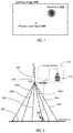
- FIG. 1is a plan view of a camera image of a selective laser sintering target.
- FIG. 2is a schematic of an example selective laser sintering system that includes a diffractive optical element that generates fiducial markers at a work surface.
- FIG. 3is another schematic of a selective laser sintering system example.
- FIG. 4is a flowchart of an example method of fiducial calibration and dynamic tracking.
- FIG. 5is a plan view of an example laser processing target.
- FIG. 6is a schematic of a laser system example.
- FIG. 7is a schematic of another laser system example.
- FIG. 8is a flowchart of an example calibration method with optical fiducials.
- values, procedures, or apparatusare referred to as “lowest”, “best”, “minimum,” or the like. It will be appreciated that such descriptions are intended to indicate that a selection among many used functional alternatives can be made, and such selections need not be better, smaller, or otherwise preferable to other selections.
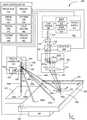
- a low power laser sourceprovides a laser beam 200 that is directed through a single or multi element diffractive optical element (DOE) 202 which splits the single beam into a plurality of beams 204 a - 204 f forming a 2-dimensional grid of beams (e.g., 10-100) that are directed to a work plane of material 206 .
- DOEdiffractive optical element
- the work plane of material 206can be a layer of metal powder which also serves to scatter the light from the DOE, such as diffusely into a partially or substantially Lambertian distribution 208 .
- the corresponding array of beams or laser projection pointscan be viewed from many angles, including through a field of view of a laser scanner 210 situated to direct an SLS processing laser beam to the work plane of material 206 .
- a laser scanner 210situated to direct an SLS processing laser beam to the work plane of material 206 .
- the grid of projection points from the DOE 202can be positionally well known in relation to the laser scanner 210 , the SLS processing laser beam, and other components of the SLS system, including the work plane of material 206 .
- a camera system 212is configured within or is optically coupled through the laser scanner so as to image the work plane of material 206 wherever the laser scanner 210 is commanded within the laser scanner field of view.
- the camera system 212can form an image 100 of the local target area directly through the scanning optics of the laser scanner 210 .
- the image 100contains the illumination fiducial 102 generated by the diffractive optical element 202 and lower power laser source.
- the camera system 212can then have both the spots 104 of the SLS laser processing beam and the DOE fiducial laser spots 102 in view. The spatial separation between the spots 102 , 104 can then be determined and the position of the laser processing beam can be adjusted based on the determined error so as to calibrate the SLS system.
- a two dimensional DOEis situated to split a single beam into a two-dimensional grid of beams each with equal angular spacing.
- a low power single mode laser beamthat can have same or similar wavelength as the SLS processing beam is directed to illuminate the DOE.
- the DOEcan be situated outside of the SLS processing chamber in which the work plane of material is situated, removing the DOE as the reference source from the high temperature conditions that can be associated with the SLS process and that could lead to distorting the reference source.
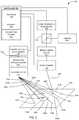
- FIG. 3shows another example of a laser system 300 that includes a laser scanner 302 situated to direct a laser processing beam 304 generated by a laser processing beam source 306 to a target 308 , such as a selective laser melting target.
- a calibration laser beam source 310generates a laser beam 312 suitable for fiducial generation through a diffractive optical element 314 .
- the diffractive optical elementreceives the laser beam 312 and generates a plurality of beamlets 316 a - 316 i that are directed through focusing optics 318 to form an array of fiducial spots 320 a - 320 i , which can be non-permanent, at the target 308 .
- the focusing optics 318provide a suitable depth of focus for the plurality of beamlets 316 a - 316 i so that an out of tolerance z-direction focus variation for the laser processing beam 304 can be detected by a camera 324 .
- Beam shaping optics 322can be situated to receive the laser processing beam 304 and adjust beam characteristics associated with the laser process (such as SLS) or associated with calibration.
- One or more of the illuminated non-permanent fiducial spots 320 a - 320 ican be viewed by the camera 324 through the laser scanner 302 and with a beam splitting element 326 that can be situated to receive a cross-section of the laser processing beam 304 , a portion of the cross-section, or adjacent to the cross-section.
- the camera 324can also view a laser processing beam spot 328 , and an image can show whether a positional error exists between the fiducial beamlet location 320 f , which can correspond to an expected location of (or expected offset from) the laser processing beam spot, and the actual location 328 of the laser processing beam spot in the field of view.
- Representative examplesoptically couple the fiducial beamlets 316 a - 316 i to the target 308 separate from the laser scanner 320 and associated optics 322 so as to thermally isolate the generation of the fiducial reference beamlets 316 a - 316 i from other components of the system.
- the fiducial beamlets 316 a - 316 ican be coupled through focusing optics of the laser scanner 302 .
- a controller 330typically includes a processor 332 , memory 334 , and one or more calibration routines 336 or algorithms that can adjust a scanning signal coupled to the laser scanner 302 based on the positional error detected with the camera 324 .
- Various field correctionscan be provided including variable corrections across the laser scanner field of view (including in a Z-direction in some examples). For example, error correction tables can be revised and polynomial or other fitting functions that describe the variation of the laser processing beam across the field of view can be updated.
- Suitable controller typescan include one or more computer devices, computing units, CPLDs, PLCs, PLDs, PALs, ASICs, etc., with each typically including one or more of the processors 332 and one or more of the memories 334 for controlling the laser processing beam source 306 , camera 324 , laser scanner 302 , and calibration laser beam source 310 .
- the memory 334can include volatile memory, such as registers, cache, and RAM, non-volatile memory, such as ROM, EEPROM, and flash memory, or a combination.
- the memory 334is accessible by the processor 332 and can store software in the form computer-executable instructions that can be executed by the processor 332 , such as the calibration routines 336 .
- the memory 334can also include removable or non-removable storage including magnetic media, CD-ROMS, DVDs, or any other medium that can be used to store information in a non-transitory way and which can be accessed within the computing environment of the controller 330 .
- the controller 330can be distributed between different components, such as between the calibration laser beam source and the laser scanner 302 , and in some examples communication is not required between all components.
- the calibration laser beam source 310 and diffractive optical element 314can be configured as a separate fiducial calibration device that can be used for different laser systems to provide calibrating optical fiducials for different laser processing targets.
- a zero positional difference for calibration purposescan correspond to a predetermined positional difference between the laser processing beam spot 328 the fiducial spots 320 a - 320 i as detected by the camera 324 .
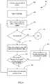
- FIG. 4is an example of a dynamic laser processing method 400 .
- a time-dependent fiducial patternis loaded into memory of a controller so that the controller can command movement of an optical fiducial, such as with a spatial light modulator that is configured to modulate an incident beam based on the fiducial pattern, across a laser processing target.
- a fiducial traceis begun corresponding to the time-dependent fiducial pattern that is applied to a laser processing target.
- the fiducial trace on the laser processing targetcan correspond to a processed target pattern of a powder layer in a selective laser sintering or other additive manufacturing process.
- Fiducial trace characteristicscan include speed and direction as well as other time-dependent characteristics, such as variation in a fiducial shape or intensity.
- an optical detectorsuch as a camera, photodiode, CMOS, CCD, array, etc., detects the fiducial of the fiducial trace and any associated fiducial characteristics through a laser scanner of a laser system situated to laser process the laser processing target.
- a modulation rate of a fiducial optical intensity or a selected fiducial shapecan be associated with an initiation of or change to a predetermined optical power or beam characteristic (including beam shape) of the laser processing beam.
- a determination of whether the fiducial is presentis made, and if it is not, the process can end at 410 .
- the laser processing beamis directed to the fiducial location with the laser scanner.
- the detected position of the fiducialcan be compared with the commanded laser processing beam position. If a position difference exists, at 416 , the position difference, corresponding to a scan error associated with a misalignment or a dynamic tracking error associated with following the optical fiducial, can be reduced by adjusting the commanded position of the laser processing beam.
- a scan error correction tablecan be updated based on the adjustment to the commanded position of the laser processing beam.
- the laser processing beamis commanded to follow the moving optical fiducial with the laser processing beam by returning, e.g., by again detecting the fiducial through the laser scanner at 406 .
- the laser processing beamcan be scanned to the newly detected position from the previous position of the laser processing beam and detected optical fiducial.
- the fiducial tracecan correspond to a welding seam, and the laser processing beam dynamically tracks the fiducial trace to form the seam based on detection of the fiducial through the laser scanner field of view.
- FIG. 5shows scanning field of view 500 for a high power laser system, such as for additive manufacturing processes, including selective laser sintering.
- the field of view 500is defined by a scan reach of a laser scanner situated to receive and scan a laser processing beam that is generated with a laser source (such as a fiber laser) across a laser processing target 502 .
- the laser scannertypically includes one or more scan mirrors, so that for a camera coupled to an optical path of the laser processing beam between the one or more scan mirrors and the laser source, a subfield field of view 504 can be defined.
- the laser processing beamforms a laser spot 506 at the laser processing target 502 in a predetermined position in the subfield field of view 504 relative to coordinate axes 508 a , 508 b .
- the laser spot 506is offset from a central position of the subfield of view 504 corresponding to the intersection of the coordinate axes 508 a , 508 b , though more typically the laser system and laser scanner are precalibrated such that laser spot 506 is directed to the central intersection position of the coordinate axes 508 a , 508 b.
- subfield field of views 510 a - 510 d similar to the subfield field of view 504can be oriented in the scanner field of view at different positions relative to the laser processing target 502 .
- the laser processing beamcan form respective laser spots 512 a - 512 d that generally have a common position in the respective subfield field of views 510 a - 510 d at the respective positions.
- the reference frame of the laser scanneris aligned and mapped to the laser processing target 502 and build plate 514 , such as in relation to a global coordinate system with a defined origin 516 .
- Such an initial calibrationcan be performed in various ways, including aligning laser scanner positions based on permanent fiducial marks on the build plate 514 , with a calibration glass plate and coordinate measurement machine, or with other techniques, including those disclosed herein.
- a plurality of optical fiducials 518 a - 518 dcan be transiently formed on the laser processing target 502 in accurate predetermined locations relative to the global coordinate system and origin 516 , and the laser scanner and laser source can be adjusted such that the laser spots 512 a - 512 d become aligned with the transient optical fiducials 518 a - 518 d .
- the transient optical fiducials 518 a - 518 dcan have various shapes, such as spots, lines, grids, cross-hairs, and annulus, though the annular shape shown in FIG. 5 is generally associated with a more rapid and/or accurate detection by an optical detector.
- displacement errorscan develop between the positions of the laser spots 512 a - 512 d and the transient optical fiducials 518 a - 518 d and across the field of view of the laser scanner, resulting in imprecisely processed targets.
- the transient optical fiducials 518 a - 518 dare detected through the laser scanner subfield field of views 510 a - 510 d and the displacement errors are determined and corrected so that the laser processing target 502 can be accurately processed with the laser processing beam.
- in-situ adjustments of the laser scanner scanning command tablecan be performed between layers of material to be laser processed to preserve laser scanning accuracies of better than 100 ⁇ m, 10 ⁇ m, or even 1 ⁇ m.
- the transient optical fiducials 518 a - 518 dcan correspond to a diffraction pattern generated with a diffractive optical element, such as a diffractive beam splitter having a predetermined pattern on a transmissive layer of material.
- the placement of the transient optical fiducials 510 a - 510 dcan have a robustness of accuracy during or between laser processing based on a spatial separation and thermal isolation of the fiducial generator with respect to the laser scanner.
- the spatial separationcan include an air separation, an adjoining boundary with the laser scanner or other components, or a thermal isolation provided with insulating material, a cooling system, etc.
- perpendicular alignments of the build plate 514 , laser processing target, and the field of view 500 relative to a zero-order axis of the fiducial generatorcan allow generation of a zero-order diffraction fiducial 520 that can be spaced apart from a center axis 522 of the laser scanner.
- the zero-order diffraction fiducial 520is outside of the field of view 500 .
- the zero-order diffraction fiducial 520can be detected and a shift or intensity variation can correspond to an out-of-tolerance condition.
- a laser system 600includes a laser source 602 situated to generate a laser processing beam 604 .
- the laser processing beam 604is typically a high power continuous, quasi-continuous, or pulsed beam.
- the laser source 602includes a gain medium 606 , such as an actively doped optical fiber amplifier, fiber oscillator, or fiber oscillator-amplifier combination, solid state block, or a plurality of semiconductor laser sources (e.g., single-emitter laser diodes, laser diode bars, etc.).
- the gain medium 606is an active fiber that is coupled to a seed source 608 , such as a diode laser or fiber oscillator, and to a pump source 610 , such as one or more fiber-coupled laser diode modules or fiber laser sources.
- a power supply 612is coupled to the pump source 610 and seed source 608 (if present) to provide an electrical power source.
- the gain medium 606can be coupled to a delivery fiber 614 that delivers to a predetermined location the laser processing beam 604 is emitted and propagates along an optical axis 615 that can correspond to a chief ray of the laser processing beam 604 .
- One or more beam shaping optics, such as a collimation optic 616are examples of the laser processing beam 604 .
- the laser processing beam 604is directed to a 2D or 3D galvanometric laser scanner 618 that typically includes one or more galvanometer scan mirrors 620 a , 620 b that are situated to rotate about respective scan mirror rotation axes 622 a , 622 b to change direction of the laser processing beam 604 as incident on a laser scan optic 624 .
- the laser scan optic 624 or one or more other optics of the laser scanner 618can be translated along the axis 615 to provide a z-focus adjustment.
- the laser processing beam 604is then directed to a selected position on a laser processing target 626 based on a deflection of the optical axis 615 with the galvanometer scan mirrors 620 a , 620 b , and z-position with the other optics of the laser scanner 618 .
- a focus in the z-directionis typically more tolerant of errors than XY positions because a depth of focus provided by the laser scanner 618 is typically many tens of microns.
- the laser scanner 618is generally configured to rotate the scan mirrors 620 a , 620 b so that the laser processing beam 604 can be directed to a predetermined area corresponding to a field of view 628 , or regard, of the laser scanner 618 .
- the laser scanner 618 and the laser source 602are coupled to a laser controller 630 .
- the laser controller 630typically includes at least one processor 632 and one or more memories 634 configured with instructions, such as a pattern command file 636 , executable by the at least one processor 632 to control beam initiation, termination, power level, repetition rate, modulation, and/or other characteristics of the laser processing beam 604 as received by the target 626 and to control beam scan position in the field of view 628 .
- instructionssuch as a pattern command file 636 , executable by the at least one processor 632 to control beam initiation, termination, power level, repetition rate, modulation, and/or other characteristics of the laser processing beam 604 as received by the target 626 and to control beam scan position in the field of view 628 .
- the scan positions in the field of view 628are mapped to the area of the target 626 so that the intended beam positions associated with the pattern command file 636 can correspond to actual beam positions on the target 626 within a predetermined lateral tolerance and/or z-tolerance (i.e., including into or out of the plane of the target 626 ).
- the mappingtypically includes the generation of an error table 637 that can include scalar correction values that provide correspondence between the field of view 628 and a global coordinate system defined for the target 626 .
- a fiducial calibrator 638can be situated in a predetermined spatial and directional relationship with respect to the target 626 .
- the fiducial calibrator 638can include a calibration laser source 640 situated to generate a fiducial source beam 642 .
- the fiducial source beam 642is typically a low power beam that can be of relatively high quality (e.g., M 2 ⁇ 5, M 2 ⁇ 2, M 2 ⁇ 1.2, etc.), and typically at a wavelength offset from a wavelength of the laser processing beam 604 .
- the fiducial source beam 642can have a same or similar wavelength as the laser processing beam 604 .
- the fiducial source beam 642is directed as a collimated beam along an optical axis 644 to a fiducial pattern generator 646 , such as a diffractive optical element.
- the fiducial pattern generator 646diffracts the fiducial source beam 642 into a plurality of fiducial beamlets 648 a - 648 e that form respective optical fiducials 650 a - 650 e that are generally transient and that have a predetermined positional relationship with the target 626 .
- the target 626includes a powder material, such as a material suitable for selective laser sintering or another additive manufacturing process, that is non-specular so as to provide a range of reflections (such as with a Lambertian or partially Lambertian profile) for incident light.
- the optical fiducials 650 a - 650 dcan be formed on this material and provide a corresponding a range of reflections, such as that shown by the different arrows directed away from the optical fiducial 650 a .
- the non-specular reflectionsare diffusive enough to provide sufficient scatter across the angle subtended between the fiducial pattern generator 646 (or other related coupling optic) and the laser scan optic 624 .
- a reflected fiducial portion 652 of the reflections of the optical fiducial 650 acan be coupled through the laser scan optic 624 and reflect off the scan mirrors 620 a , 620 b .
- a beam splitter 654 or other suitable wavelength-dependent beam-directing opticcan be situated in the path of the laser processing beam 604 to receive and direct the reflected fiducial portion 652 (e.g., through reflection, refraction, transmission, a combination, etc.) to an optical detector 656 , such as a camera, one or more photodiodes, CCDs, CMOS sensors, arrays, etc.
- the optical detector 656has a movable field of view 658 that is defined by the optical path between the optical detector 656 and the target 626 , including the scan position and mirror areas of the scan mirrors 620 a , 620 b .
- the field of view 658 of the optical detector 656is optically aligned with respect to the propagation axis 615 such that a center of the field of view 658 corresponds to the position of the spot of the laser processing beam 604 at the target 626 during processing, though other alignments are possible.
- the controller 630can be coupled to the fiducial calibrator 638 and the optical detector 656 to cause the fiducial calibrator 638 to generate the optical fiducials 650 a - 650 d and to receive a detection signal from the optical detector 656 .
- the received detection signalcan correspond to detected optical characteristics of the optical fiducial 650 a with the field of view 658 positioned in view of optical fiducial 650 a , or detected optical characteristics of the optical fiducials 650 b - 650 d with the scan mirrors 620 a , 620 b moved so that the field of view 658 moves to be in view of the respective optical fiducials 650 b - 650 d .
- the fiducial calibrator 638is sufficiently thermally separated from the laser scanner 618 and laser source 602 to reduce a position error of the optical fiducials 650 a - 650 d at the target 626 , e.g., through spatial separation and/or thermal cooling of the fiducial calibrator.
- the target 626can include a build plate base 662 that is lowered with a z-stage 664 with a z-stage control 666 of the controller 630 .
- a layer of powder materialis provided above the build plate base 662 and a pushing bar 668 can be used to flatten the surface of the powder material and remove excess material so that the top of the powder layer corresponds with a predetermined plane for a focus of the laser processing beam 604 at the target 626 .
- the build plate base 662can lower with the z-stage 664 and an additional layer of powder can be deposited and flattened so that the additional layer can be processed with the laser processing beam 604 .
- the z-stage 664can also provide x, y, or xy translation, or can include a conveyor system that translates the target 626 .
- a calibration routine 660can be performed with the controller 630 at a manually selected time, or during one or more automatically selected times or intervals, including at a start or end of a process, during laser processing with the laser processing beam 604 , or between laser processes or processing steps, such as between processing of layers of powder material.
- the calibration routine 660can include a fiducial command 670 that includes causing the fiducial calibrator 638 to produce the optical fiducials 650 a - 650 d at the target 626 .
- the optical fiducials 650 a - 650 dcan be transiently directed to the target 626 while one or more components of the laser system 300 is powered.
- the scan mirrors 620 a , 620 bare directed to predetermined positions associated with the optical fiducials 650 a - 650 d , and the optical detector 656 detects the position of the optical fiducials 650 a - 650 d in the field of view 658 at each position. Based on the detected positions, a positional error can be determined, and the error correction table 637 can be updated, typically using one or more interpolation/extrapolation techniques, to determine suitable correction values for other scan positions in the field of view 628 .
- the fiducial beamlet 648 e generated with the fiducial calibrator 638can correspond to a zero-order diffraction produced by the fiducial pattern generator 646 .
- the optical fiducial 650 ecan be formed on a separate surface 672 adjacent to the target 626 , or can be formed on the target 626 in some examples.
- a beam splitter 674can be situated to direct a portion of a reflected beam 676 that is received from the surface 672 to an optical detector 678 , e.g., through a pinhole aperture 680 .
- other beam directing opticsthat are not situated in the path of the fiducial beamlet 648 e can be used instead of the beam splitter 674 .
- Misalignments or alignment variations between the fiducial calibrator 638 and the surface 672 and target 626can be detected based on a variation in the detected zero-order reflected beam 676 , such as a drift in reflected beam position which can correspond to an angular variation of the surface 672 relative to the fiducial beamlet 648 e .
- the optical detector 678can be coupled to the laser controller 630 and a fiducial error detection routine 682 can form an interlock with operation of the laser source 602 , can indicate a misalignment exists, or that the fiducial calibrator 638 has accrued a decrease in fiducial accuracy, by way of example.
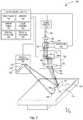
- FIG. 7is a laser system 700 that is configured for dynamic transient optical fiducial placement and tracking.
- the laser system 700includes a laser source 702 situated to produce a laser beam 704 , which is typically emitted from a delivery fiber 706 .
- the laser beam 704coupled via free-space, a beam homogenizer, and/or other optics.
- the laser beam 704is directed along a propagation axis 705 to a laser scanner 706 that includes a pair of scan mirrors 708 a , 708 b generally rotatable about respective orthogonal axes 710 a , 710 b with galvanometer actuators to change a direction of the received laser beam 704 .
- a focus optic 712receives the laser beam 704 and focuses the laser beam 704 a laser processing target 714 , such as a welding target, cutting target, patterning target, selective laser sintering target, additive manufacturing target, etc.
- a laser controller 716is coupled to the laser source 702 and the laser scanner 706 to control beam characteristics of the laser beam 704 , such as power, wavelength, repetition rate, spot intensity/divergence profile and/or geometry, etc.
- the laser controllertypically includes at least one processor 718 and at least one memory 720 configured with various instructions and data storage so that the processor 718 in response to the instructions in the memory 720 can cause the laser source 702 to emit the laser beam 704 and cause the laser scanner 706 to vary a scan position so that the laser beam 704 forms a laser spot 722 at the laser processing target 714 .
- the laser system 700also includes fiducial calibrator 724 situated to direct an optical fiducial 726 to, and change a fiducial position at, the laser processing target 714 .
- the fiducial calibrator 724can be situated separately from the laser scanner 706 , though the spatial separation can be vary in different examples.
- the fiducial calibrator 724can be mechanically attached to the laser scanner 706 or situated in close proximity to the laser scanner 706 , though the fiducial calibrator 724 is typically configured with a sufficiently separate spatial distance and/or coupling such that a calibration between the fiducial calibrator 724 and the laser processing target 714 remains unchanged or varies independently from a calibration decrease between the laser scanner 706 and the laser processing target 714 .
- the fiducial calibrator 726includes an optical source 728 , such as a laser, LED, etc., situated generate a fiducial source beam 730 , and a spatial light modulator 732 situated to receive and spatially modulate the fiducial source beam 730 to selectively provide the optical fiducial 726 in a selective position across a field of regard 734 or a portion of the field of regard 734 that corresponds to a scan reach of laser beam 704 with the laser scanner 706 .
- Suitable examples of the spatial light modulator 732include a digital micro-mirror device (DMD), liquid crystal on silicon (LCoS) device, acousto-optic modulator, or electro-optic modulator, by way of example.
- the laser controller 716is coupled to the fiducial calibrator 724 and configured with a fiducial movement command 736 to change the position of the optical fiducial 726 .
- the fiducial movement command 736 and the fiducial calibrator 724can be coupled to a separate controller that is not in communication with the laser controller 716 .
- An optical detector 738is situated to receive a reflected beam portion 740 of the optical fiducial 726 .
- the laser processing target 714has a surface that does not produce an exclusively specular reflection such that a portion of light reflected by laser processing target 714 , corresponding to the reflected beam portion 740 , is directed through the laser scan optic 712 and the scan mirrors 708 a , 708 b , to a selective optic 742 that directs the reflected beam portion 740 to the optical detector 738 .
- the optical detector 738can have a field of view 744 that can be defined in part by the position of the scan mirrors 708 a , 708 b .
- the optical detector 738can detect the laser spot 722 and the optical fiducial 726 , and the laser controller 716 can receive the detection signal to determine a positional difference between the laser spot 722 and the optical fiducial 726 .
- the laser spot 722is aligned with a predetermined position (e.g., a center) in the field of view 744 and the positional difference is determined based on the predetermined position and the detected position of the optical fiducial 726 .
- the laser controller 716can be provided with an expected position of the laser spot 722 based on the fiducial movement command 736 .
- the laser controller 716can command the laser scanner 706 through a range of scan positions to detect the optical fiducial 726 in the field of regard 734 .
- the laser controller 716can include a fiducial tracking command 750 that causes the laser controller 716 to adjust a scan position of the laser spot 722 to a new position that reduces the positional difference between the optical fiducial 726 and the laser spot 722 .
- the adjustmentis typically performed in real-time so that the laser spot 722 can follow the time-dependent processing trace 746 .
- various closed-loop control methodscan be used to provide convergence or substantial reductions in position errors to allow the laser spot 722 to follow the optical fiducial 726 to the new position of the optical fiducial 748 , including but not limited to PID, PI, lead-lag, etc.
- the detected positions of the optical fiducial 726 and later positions of the optical fiducial, such as along the processing trace 746can be stored in the memory 720 so that the laser beam 704 can be moved to positions after the optical fiducial has moved or is no longer in the field of regard 734 or the field of view 744 .
- the fiducial tracking command 750can also cause the laser source 702 or associated beam shaping optics to adjust characteristics of the laser spot 722 , such as diameter, shape, irradiance, etc., based on changes between the detected optical fiducials 726 , 748 .
- beam shaping opticscan include fiber-based beam shaping, zoom expansion, relative movement of lenses, mirrors, or other optical components that vary a beam characteristic.
- the laser processing target 714can include a plurality of adjacent subtargets and the time-dependent processing trace 746 can follow along a boundary of the adjacent subtargets.
- the fiducial calibrator 724can also be configured with the laser controller 718 and the optical detector 738 to provide a calibration routine 752 that can provide scan rotation correction values (e.g., rotation increments for the scan mirrors 708 a , 708 b ) for scanning of the laser beam 704 across the field of regard 734 .
- the fiducial calibrator 724can direct optical fiducials to predetermined calibration locations in the field of regard 734 , such as to the positions shown for the optical fiducials 726 , 748 , or other locations.
- the optical detector 738can detect a position difference between the respective optical fiducials 726 , 748 and a spot of the laser beam 704 or a predetermined position in the field of view 744 of the optical detector 738 .
- the laser controller 716can include a scan actuator error correction table 754 that can includes scan actuator bit corrections for the scan mirrors 708 a , 708 b so that the laser beam 704 can form the laser spot 722 in locations in the field of regard 734 that accurately correspond to global coordinates of the laser processing target 714 .
- the laser scanner 706can include scanning capability in the z-direction and the error correction table 754 can also include scan actuator bit corrections for the z-direction.
- the scan actuator error correction table 754can be updated with error correction values based on the positional differences detected and determined with the calibration routine 752 .
- the detector 738can detect positional errors, such as a variation in focus based on change in fiducial spot size or blur associated with defocus.
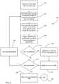
- FIG. 8is a method 800 of calibrating a laser processing target and laser system with a fiducial calibrator.
- a plurality of optical fiducialsare generated with the fiducial calibrator and directed to a laser processing target, typically along an axis separate from an associated laser scanner situated to scan a laser processing beam of the laser system in relation to the target (e.g., along X, Y, and/or Z directions).
- the optical fiducialsare generally transiently generated such that the surface of the laser processing target is not permanently marked by the optical fiducials or such that the laser processing target need not be permanently marked for calibration and/or detection based on the optical fiducials.
- the laser scanneris commanded with a laser controller to direct the laser processing beam at a process power, at a low power, or unpowered to a position in a field of regard of the laser scanner that corresponds to the expected location of a selected one of the plurality of optical fiducials.
- the selected one of the optical fiducialsis detected in a subfield of the field of regard of the laser scanner with an optical detector (such as a camera) based on the optical coupling to the laser processing target of the optical detector through the laser scanner.
- the laser controllercompares the detected optical fiducial location with the expected location and determines a position error, such as one or more of an X, Y, and Z position error.
- the laser controllerchecks if the determined position error is outside of a tolerance condition, such as less than 50 ⁇ m, 20 ⁇ m, 10 ⁇ m, 5 ⁇ m, 3 ⁇ m, 1 ⁇ m, etc. If the position error is out of tolerance, at 812 , the controller determines a scan actuation correction for the laser scanner that reduces the error. At 814 , an error correction table is updated in the laser controller with the correction that produces the error reduction for the commanded position of the laser scanner and laser processing beam.
- a tolerance conditionsuch as less than 50 ⁇ m, 20 ⁇ m, 10 ⁇ m, 5 ⁇ m, 3 ⁇ m, 1 ⁇ m, etc.
- a checkis performed as to whether the last optical fiducial of the plurality of optical fiducials has been detected and compared, and can also be performed if the check for an error of a selected optical fiducial yield an in-tolerance condition. If there are additional optical fiducials to be checked, at 818 , another of the plurality of optical fiducials can be selected and the process steps 804 onward can be performed until all optical fiducials are detected and analyzed.
- additional correctionscan be applied for other areas or regions in the field of regard of the laser scanner where optical fiducials were not directed and the error table can be updated with new correction values or new values associated with correction values.
- the additional corrections for other positions in the field of regardcan be determined with linear or curve fitting algorithms based on the corrections associated with the optical fiducials. Suitable methods of correcting scan actuation values include those disclosed in U.S. patent application Ser. No. 15/410,612, entitled “Method of processing calibration data in 3D laser scanner systems,” which is incorporated by reference herein in its entirety.
- Correctionscan be applied across the field of regard of the laser scanner at different nodes (e.g., forming one or more grids of x, y, and/or z coordinates) based on higher order polynomials fit to the corrections or derivatives of such functions.
- An initial set of correctionscan be provided based on a computational model characterizing the laser scanner and optics associated with direct the laser processing beam to the target. Corrections for non-nodal locations can be determined from interpolation between adjacent correction nodes.
Landscapes
- Engineering & Computer Science (AREA)
- Chemical & Material Sciences (AREA)
- Materials Engineering (AREA)
- Manufacturing & Machinery (AREA)
- Physics & Mathematics (AREA)
- Health & Medical Sciences (AREA)
- General Health & Medical Sciences (AREA)
- Toxicology (AREA)
- Automation & Control Theory (AREA)
- General Physics & Mathematics (AREA)
- Optics & Photonics (AREA)
- Analytical Chemistry (AREA)
- Plasma & Fusion (AREA)
- Laser Beam Processing (AREA)
Abstract
Description
Claims (20)
Priority Applications (4)
| Application Number | Priority Date | Filing Date | Title |
|---|---|---|---|
| US15/945,550US11173548B2 (en) | 2017-04-04 | 2018-04-04 | Optical fiducial generation for galvanometric scanner calibration |
| US16/557,863US11389896B2 (en) | 2017-04-04 | 2019-08-30 | Calibration test piece for galvanometric laser calibration |
| US17/501,932US11982819B2 (en) | 2017-04-04 | 2021-10-14 | Optical fiducial generation for galvanometric scanner calibration |
| US18/636,766US20240264457A1 (en) | 2017-04-04 | 2024-04-16 | Optical fiducial generation for galvanometric scanner calibration |
Applications Claiming Priority (2)
| Application Number | Priority Date | Filing Date | Title |
|---|---|---|---|
| US201762481637P | 2017-04-04 | 2017-04-04 | |
| US15/945,550US11173548B2 (en) | 2017-04-04 | 2018-04-04 | Optical fiducial generation for galvanometric scanner calibration |
Related Child Applications (2)
| Application Number | Title | Priority Date | Filing Date |
|---|---|---|---|
| US16/557,863Continuation-In-PartUS11389896B2 (en) | 2017-04-04 | 2019-08-30 | Calibration test piece for galvanometric laser calibration |
| US17/501,932ContinuationUS11982819B2 (en) | 2017-04-04 | 2021-10-14 | Optical fiducial generation for galvanometric scanner calibration |
Publications (2)
| Publication Number | Publication Date |
|---|---|
| US20180281067A1 US20180281067A1 (en) | 2018-10-04 |
| US11173548B2true US11173548B2 (en) | 2021-11-16 |
Family
ID=62152616
Family Applications (3)
| Application Number | Title | Priority Date | Filing Date |
|---|---|---|---|
| US15/945,550Active2040-01-03US11173548B2 (en) | 2017-04-04 | 2018-04-04 | Optical fiducial generation for galvanometric scanner calibration |
| US17/501,932Active2038-04-15US11982819B2 (en) | 2017-04-04 | 2021-10-14 | Optical fiducial generation for galvanometric scanner calibration |
| US18/636,766PendingUS20240264457A1 (en) | 2017-04-04 | 2024-04-16 | Optical fiducial generation for galvanometric scanner calibration |
Family Applications After (2)
| Application Number | Title | Priority Date | Filing Date |
|---|---|---|---|
| US17/501,932Active2038-04-15US11982819B2 (en) | 2017-04-04 | 2021-10-14 | Optical fiducial generation for galvanometric scanner calibration |
| US18/636,766PendingUS20240264457A1 (en) | 2017-04-04 | 2024-04-16 | Optical fiducial generation for galvanometric scanner calibration |
Country Status (5)
| Country | Link |
|---|---|
| US (3) | US11173548B2 (en) |
| EP (1) | EP3607389B1 (en) |
| KR (1) | KR102611837B1 (en) |
| CN (1) | CN110651218B (en) |
| WO (1) | WO2018187489A1 (en) |
Cited By (1)
| Publication number | Priority date | Publication date | Assignee | Title |
|---|---|---|---|---|
| US11465232B2 (en)* | 2014-06-05 | 2022-10-11 | Nlight, Inc. | Laser patterning skew correction |
Families Citing this family (48)
| Publication number | Priority date | Publication date | Assignee | Title |
|---|---|---|---|---|
| US9403235B2 (en) | 2014-06-20 | 2016-08-02 | Velo3D, Inc. | Apparatuses, systems and methods for three-dimensional printing |
| CN108367498A (en) | 2015-11-06 | 2018-08-03 | 维洛3D公司 | ADEPT 3 D-printings |
| CN108698126A (en) | 2015-12-10 | 2018-10-23 | 维洛3D公司 | Consummate 3 D-printing |
| US9919360B2 (en) | 2016-02-18 | 2018-03-20 | Velo3D, Inc. | Accurate three-dimensional printing |
| WO2018005439A1 (en) | 2016-06-29 | 2018-01-04 | Velo3D, Inc. | Three-dimensional printing and three-dimensional printers |
| WO2018064349A1 (en) | 2016-09-30 | 2018-04-05 | Velo3D, Inc. | Three-dimensional objects and their formation |
| WO2018128695A2 (en) | 2016-11-07 | 2018-07-12 | Velo3D, Inc. | Gas flow in three-dimensional printing |
| US20180186081A1 (en)* | 2017-01-05 | 2018-07-05 | Velo3D, Inc. | Optics in three-dimensional printing |
| US10442003B2 (en) | 2017-03-02 | 2019-10-15 | Velo3D, Inc. | Three-dimensional printing of three-dimensional objects |
| US20180281282A1 (en) | 2017-03-28 | 2018-10-04 | Velo3D, Inc. | Material manipulation in three-dimensional printing |
| US11389896B2 (en) | 2017-04-04 | 2022-07-19 | Nlight, Inc. | Calibration test piece for galvanometric laser calibration |
| US10272525B1 (en) | 2017-12-27 | 2019-04-30 | Velo3D, Inc. | Three-dimensional printing systems and methods of their use |
| JP2022506523A (en) | 2018-11-02 | 2022-01-17 | インクビット, エルエルシー | Intelligent addition manufacturing method |
| US11354466B1 (en) | 2018-11-02 | 2022-06-07 | Inkbit, LLC | Machine learning for additive manufacturing |
| DE102018127989A1 (en)* | 2018-11-08 | 2020-05-14 | Trumpf Laser- Und Systemtechnik Gmbh | Method for operating a device for the additive production of a three-dimensional object |
| DE102018128279A1 (en)* | 2018-11-12 | 2020-05-14 | Aconity Gmbh | Improved calibration procedure for a system for powder bed-based generation of three-dimensional components using electromagnetic radiation |
| AU2019378044A1 (en) | 2018-11-16 | 2021-05-27 | Inkbit, LLC | Inkjet 3D printing of multi-component resins |
| WO2020146481A1 (en) | 2019-01-08 | 2020-07-16 | Inkbit, LLC | Reconstruction of surfaces for additive manufacturing |
| AU2020206336A1 (en) | 2019-01-08 | 2021-07-15 | Inkbit, LLC | Depth reconstruction in additive fabrication |
| WO2020153995A1 (en) | 2019-01-23 | 2020-07-30 | Nlight, Inc. | A galvanometric laser system with a calibration test piece |
| US11679551B2 (en)* | 2019-02-28 | 2023-06-20 | General Electric Company | Compensating laser alignment for irregularities in an additive manufacturing machine powderbed |
| US11525968B2 (en) | 2019-03-14 | 2022-12-13 | Nlight, Inc. | Calibration validation using geometric features in galvanometric scanning systems |
| US11579440B2 (en) | 2019-03-14 | 2023-02-14 | Nlight, Inc. | Focus assessment in dynamically focused laser system |
| EP3938177B1 (en)* | 2019-03-15 | 2024-05-01 | Formlabs, Inc. | Method and system for calibration of optics modules for additive fabrication devices |
| EP3736110A1 (en)* | 2019-05-09 | 2020-11-11 | LayerWise NV | System for aligning laser system to a carrier plate |
| JP7130596B2 (en)* | 2019-05-21 | 2022-09-05 | 株式会社荏原製作所 | AM Apparatus for Manufacturing Modeled Object and Method for Testing Beam Irradiation Position in AM Apparatus |
| US12103107B2 (en) | 2019-07-18 | 2024-10-01 | General Electric Company | System and methods for compensating for calibration plate irregularities in additive manufacturing systems |
| KR20220031745A (en) | 2019-07-26 | 2022-03-11 | 벨로3디, 인크. | Quality assurance for 3D object shaping |
| CN114302782B (en)* | 2019-08-27 | 2024-04-26 | 尼康Slm方案股份公司 | Equipment and systems for manufacturing three-dimensional parts using additive manufacturing technology |
| WO2021046076A1 (en)* | 2019-09-04 | 2021-03-11 | Vulcanforms Inc. | Laser array position detection |
| US10994477B1 (en) | 2019-11-01 | 2021-05-04 | Inkbit, LLC | Optical scanning for industrial metrology |
| US11712837B2 (en) | 2019-11-01 | 2023-08-01 | Inkbit, LLC | Optical scanning for industrial metrology |
| US11049272B1 (en) | 2019-12-31 | 2021-06-29 | Shutterfly, Llc | System for assembling composite group image from individual subject images |
| US10994490B1 (en)* | 2020-07-31 | 2021-05-04 | Inkbit, LLC | Calibration for additive manufacturing by compensating for geometric misalignments and distortions between components of a 3D printer |
| US12309327B2 (en) | 2021-02-24 | 2025-05-20 | General Electric Company | Automated beam scan calibration, alignment, and adjustment |
| JP6978137B1 (en)* | 2021-07-15 | 2021-12-08 | 株式会社松浦機械製作所 | 3D modeling equipment |
| CN113579854B (en)* | 2021-07-21 | 2022-07-29 | 安庆中船动力配套有限公司 | Automatic correction system based on diesel engine connecting rod machining machine tool |
| CN114054941B (en)* | 2021-10-29 | 2024-07-09 | 西安铂力特增材技术股份有限公司 | Vibrating mirror calibration plate, device and vibrating mirror calibration method |
| US12397376B2 (en)* | 2022-04-28 | 2025-08-26 | Rtx Corporation | Off-axis laser beam measurement for laser powder bed fusion |
| US12392658B2 (en)* | 2022-05-09 | 2025-08-19 | Edison Welding Institute, Inc. | In-motion laser beam analysis and analysis at field of view extremities for high-speed laser motion systems |
| WO2023237318A1 (en)* | 2022-06-07 | 2023-12-14 | Nikon Slm Solutions Ag | Calibration method and printing system configured to produce a three-dimensional workpiece |
| DE102022116899A1 (en) | 2022-07-06 | 2024-01-11 | 4Jet Microtech Gmbh | Processing device and method |
| NL2033096B1 (en)* | 2022-09-21 | 2024-03-26 | Additive Ind Bv | An apparatus for producing an object by means of additive manufacturing and a method of calibrating the apparatus |
| CN116000444A (en)* | 2022-12-30 | 2023-04-25 | 武汉锐科光纤激光技术股份有限公司 | Laser processing device and processing method of laser processing device |
| WO2024201364A1 (en)* | 2023-03-31 | 2024-10-03 | Dwfritz Automation, Llc | Locating and sizing 2d imaged features in 3d laser scanning coordinate system |
| GB2636399A (en)* | 2023-12-12 | 2025-06-18 | Wayland Additive Ltd | Method of calibrating a digital image recording device |
| WO2025155634A1 (en)* | 2024-01-17 | 2025-07-24 | Nlight, Inc. | Scanner calibration for additive manufacturing in a three dimensional printer incorporating zoom optics |
| US20250269461A1 (en)* | 2024-02-27 | 2025-08-28 | Freeform Future Corp. | Laser alignment in 3d printing system |
Citations (205)
| Publication number | Priority date | Publication date | Assignee | Title |
|---|---|---|---|---|
| US3388461A (en) | 1965-01-26 | 1968-06-18 | Sperry Rand Corp | Precision electrical component adjustment method |
| US4315666A (en) | 1979-03-19 | 1982-02-16 | Hicks Jr John W | Coupled communications fibers |
| EP0048855A2 (en) | 1980-09-29 | 1982-04-07 | Siemens Aktiengesellschaft | Element for adjusting the transfer of light between light guides |
| JPS6046892A (en) | 1984-07-19 | 1985-03-13 | Toshiba Corp | Laser light irradiation method |
| US4713518A (en) | 1984-06-08 | 1987-12-15 | Semiconductor Energy Laboratory Co., Ltd. | Electronic device manufacturing methods |
| US4863538A (en) | 1986-10-17 | 1989-09-05 | Board Of Regents, The University Of Texas System | Method and apparatus for producing parts by selective sintering |
| JPH02220314A (en) | 1989-02-21 | 1990-09-03 | Teikoku Tsushin Kogyo Co Ltd | Electronic component resin mold case with built-in flexible board and its manufacturing method |
| US4953947A (en) | 1986-08-08 | 1990-09-04 | Corning Incorporated | Dispersion transformer having multichannel fiber |
| US5008555A (en) | 1988-04-08 | 1991-04-16 | Eaton Leonard Technologies, Inc. | Optical probe with overlapping detection fields |
| US5082349A (en) | 1988-04-25 | 1992-01-21 | The Board Of Trustees Of The Leland Stanford Junior University | Bi-domain two-mode single crystal fiber devices |
| JPH04112355A (en) | 1990-09-03 | 1992-04-14 | Wacom Co Ltd | Self-learning type analog neuron circuit |
| US5129014A (en) | 1989-12-08 | 1992-07-07 | Xerox Corporation | Image registration |
| US5252991A (en) | 1991-12-17 | 1993-10-12 | Hewlett-Packard Company | Media edge sensor utilizing a laser beam scanner |
| RU2008742C1 (en) | 1991-03-04 | 1994-02-28 | Рыков Вениамин Васильевич | Process of doping of semiconductors |
| RU2021881C1 (en) | 1986-10-17 | 1994-10-30 | Борд оф Риджентс, Дзе Юниверсити оф Тексас Систем | Method to produce a part and the device to fulfill it |
| WO1995011100A1 (en) | 1993-10-20 | 1995-04-27 | United Technologies Corporation | Temperature-controlled laser sintering |
| WO1995011101A1 (en) | 1993-10-20 | 1995-04-27 | United Technologies Corporation | Multiple beam laser sintering |
| US5509597A (en) | 1994-10-17 | 1996-04-23 | Panasonic Technologies, Inc. | Apparatus and method for automatic monitoring and control of a soldering process |
| DE4437284A1 (en) | 1994-10-18 | 1996-04-25 | Eos Electro Optical Syst | Method for calibrating a controller to deflect a laser beam |
| US5523543A (en) | 1994-09-09 | 1996-06-04 | Litel Instruments | Laser ablation control system and method |
| US5566196A (en) | 1994-10-27 | 1996-10-15 | Sdl, Inc. | Multiple core fiber laser and optical amplifier |
| US5642198A (en) | 1995-04-03 | 1997-06-24 | Long; William R. | Method of inspecting moving material |
| US5719386A (en) | 1996-02-07 | 1998-02-17 | Umax Data Systems, Inc. | High efficiency multi-image scan method |
| JPH10282450A (en) | 1997-04-02 | 1998-10-23 | Nippon Steel Corp | Binary optics and laser processing apparatus using the same |
| US5837962A (en) | 1996-07-15 | 1998-11-17 | Overbeck; James W. | Faster laser marker employing acousto-optic deflection |
| US5841465A (en) | 1995-09-29 | 1998-11-24 | Fuji Xerox Co., Ltd. | Light beam focal position detecting device, light beam projecting device, and light beam recording apparatus |
| US5932119A (en) | 1996-01-05 | 1999-08-03 | Lazare Kaplan International, Inc. | Laser marking system |
| JPH11231138A (en) | 1998-02-10 | 1999-08-27 | Fujikura Ltd | Optical filter and optical communication system |
| CA2292974A1 (en) | 1998-12-22 | 2000-06-22 | The Board Of Trustees Of The Leland Stanford Junior University | Tunable, mechanically induced long-period fiber grating with enhanced polarizing characteristics |
| US6192171B1 (en) | 1999-02-26 | 2001-02-20 | Albert Goodman | Dynamic fiber optic switch with artificial muscle |
| US6275630B1 (en) | 1998-11-17 | 2001-08-14 | Bayspec, Inc. | Compact double-pass wavelength multiplexer-demultiplexer |
| WO2001074529A2 (en) | 2000-03-30 | 2001-10-11 | Electro Scientific Industries, Inc. | Laser system and method for single pass micromachining of multilayer workpieces |
| US20010045149A1 (en) | 1998-12-31 | 2001-11-29 | Maurice Granger | Device for controlling ejection of cutting blade of a drum in a wipe material dispensing machine |
| US20010050364A1 (en) | 2000-03-08 | 2001-12-13 | Semiconductor Energy Laboratory Co., Ltd. | Semiconductor device and manufacturing method thereof |
| US6353203B1 (en) | 1997-12-26 | 2002-03-05 | Mitsubishi Denki Kabushiki Kaisha | Laser machining device |
| US6360042B1 (en) | 2001-01-31 | 2002-03-19 | Pin Long | Tunable optical fiber gratings device |
| USRE37585E1 (en) | 1994-04-08 | 2002-03-19 | The Regents Of The University Of Michigan | Method for controlling configuration of laser induced breakdown and ablation |
| US6362004B1 (en) | 1999-11-09 | 2002-03-26 | Packard Biochip Technologies, Llc | Apparatus and method for using fiducial marks on a microarray substrate |
| US6426840B1 (en) | 2001-02-23 | 2002-07-30 | 3D Systems, Inc. | Electronic spot light control |
| US6434302B1 (en) | 1998-03-04 | 2002-08-13 | Jds Uniphase Corporation | Optical couplers for multimode fibers |
| EP1238745A2 (en) | 2001-03-07 | 2002-09-11 | Nec Corporation | Galvanometer controller and laser machining apparatus |
| US6477301B1 (en) | 1997-06-26 | 2002-11-05 | Scientific-Atlanta, Inc. | Micro-optic coupler incorporating a tapered fiber |
| US6490376B1 (en) | 1998-09-17 | 2002-12-03 | Metrologic Instruments, Inc. | Skew processing of raster scan images |
| US20030001743A1 (en) | 1998-10-23 | 2003-01-02 | Menard Raymond J. | Personal medical device communication system and method |
| US6577314B1 (en) | 1992-07-14 | 2003-06-10 | Canon Kabushiki Kaisha | Character generation using data of plural types to which differing priorities are assigned |
| US6600149B2 (en) | 1999-12-27 | 2003-07-29 | Whitten L. Schulz | Fiber grating environmental sensing system |
| CN1445600A (en) | 2002-03-15 | 2003-10-01 | 美国飞泰尔有限公司 | Computer program product, system and method for adjustable multimode wave division multi-channel multiplex Raman pump |
| US20030213998A1 (en) | 2002-05-16 | 2003-11-20 | International Business Machines Corporation | Variable resistor structure and method for forming and programming a variable resistor for electronic circuits |
| US20040031779A1 (en) | 2002-05-17 | 2004-02-19 | Cahill Steven P. | Method and system for calibrating a laser processing system and laser marking system utilizing same |
| DE20320269U1 (en) | 2003-03-28 | 2004-04-15 | Raylase Ag | Optical system with adjustable total length for variable focussing of light (laser) beam, with lens module in light beam path for laser 3D scanners also for writing, marking, cutting |
| US20040112634A1 (en) | 2001-03-02 | 2004-06-17 | Hirokazu Tanaka | Method for plating polymer molding material, circuit forming component and method for producing circuit forming component |
| US20040207936A1 (en) | 2003-04-17 | 2004-10-21 | Toshio Yamamoto | Lens driving apparatus, thin camera, and a cellular phone having a thin camera |
| US20040247222A1 (en) | 2003-03-27 | 2004-12-09 | Lg Electronics, Inc. | Laser display device and method for controlling the same |
| WO2005053895A1 (en) | 2003-12-05 | 2005-06-16 | Spi Lasers Uk Limited | Apparatus for the industrial processing of a material by optical radiation |
| JP2005203430A (en) | 2004-01-13 | 2005-07-28 | Mitsubishi Cable Ind Ltd | Optical fiber laser and laser beam generating method using the same |
| US20050168847A1 (en) | 2004-02-03 | 2005-08-04 | Pentax Corporation | Lens moving mechanism |
| US20050191017A1 (en) | 1999-12-24 | 2005-09-01 | Andre Croteau | Multi-clad doped optical fiber |
| JP2006106227A (en) | 2004-10-01 | 2006-04-20 | Hokkaido Univ | Laser processing method and apparatus |
| TW200633062A (en) | 2004-11-05 | 2006-09-16 | Koninkl Philips Electronics Nv | Method for patterning an organic material to concurrently form an insulator and a semiconductor and device formed thereby |
| US20060215976A1 (en) | 2005-03-22 | 2006-09-28 | Matsushita Electric Industrial Co., Ltd. | Multicore optical fiber with integral diffractive elements machined by ultrafast laser direct writing |
| US20060275705A1 (en) | 2005-06-01 | 2006-12-07 | Hewlett-Packard Development Company Lp | Conductive patterning |
| US7151788B2 (en) | 2001-12-28 | 2006-12-19 | Fujitsu Limited | Laser processing device |
| TWI271904B (en) | 2001-03-29 | 2007-01-21 | Gsi Lumonics Corp | High-speed, precision, laser-based method and system |
| US20070047940A1 (en) | 2005-08-30 | 2007-03-01 | Kosei Matsumoto | Image input device and calibration method |
| CN1926460A (en) | 2004-04-28 | 2007-03-07 | 奥林巴斯株式会社 | Laser focusing optical system |
| US7196339B2 (en) | 2003-05-30 | 2007-03-27 | Olympus Corporation | Light-receiving unit and measuring apparatus including the same |
| US20070075060A1 (en) | 2005-09-30 | 2007-04-05 | Shedlov Matthew S | Method of manufacturing a medical device from a workpiece using a pulsed beam of radiation or particles having an adjustable pulse frequency |
| CN1966224A (en) | 2005-11-16 | 2007-05-23 | 达里尔·J·科斯廷 | New substrates for engineered wood fiber products and methods of forming substrates by laser processing |
| US7231063B2 (en) | 2002-08-09 | 2007-06-12 | Intersense, Inc. | Fiducial detection system |
| US20070206900A1 (en) | 2001-03-30 | 2007-09-06 | Nufern | Ring Core Fiber |
| US20070251543A1 (en) | 2006-04-28 | 2007-11-01 | Asml Netherlands B.V. | Methods to clean a surface, a device manufacturing method, a cleaning assembly, cleaning apparatus, and lithographic apparatus |
| CN101071926A (en) | 2007-05-30 | 2007-11-14 | 天津大学 | Active Q-switched full-optical-fiber laser |
| RU68715U1 (en) | 2006-11-20 | 2007-11-27 | Государственное образовательное учреждение высшего профессионального образования "Кубанский государственный университет" (ГОУ ВПО КубГУ) | INTEGRAL OPTICAL RADIATION DIVIDER |
| CN101133351A (en) | 2004-12-30 | 2008-02-27 | 普罗克斯米奥恩纤维系统公司 | Optical coupler |
| CN101143405A (en) | 2006-09-12 | 2008-03-19 | 株式会社迪思科 | Laser processing device |
| US7349123B2 (en) | 2004-03-24 | 2008-03-25 | Lexmark International, Inc. | Algorithms and methods for determining laser beam process direction position errors from data stored on a printhead |
| JP4112355B2 (en) | 2002-12-11 | 2008-07-02 | 日立造船株式会社 | Beam forming method and apparatus |
| US20080231939A1 (en) | 2005-03-18 | 2008-09-25 | Danmarks Tekniske Universitet | Optical Manipulation System Using a Plurality of Optical Traps |
| EP1974848A1 (en) | 2007-03-30 | 2008-10-01 | Innolas GmbH | System and and the method thereof for correcting a laser beam deflection device |
| US20080251504A1 (en) | 2007-04-11 | 2008-10-16 | Feng Lu | Laser-welding apparatus and method |
| CN101303269A (en) | 2007-05-09 | 2008-11-12 | 奥林巴斯株式会社 | Optical system evaluation apparatus, optical system evaluation method and program thereof |
| CN101314196A (en) | 2007-05-28 | 2008-12-03 | 三菱电机株式会社 | Laser processing device |
| CN101403822A (en) | 2007-10-01 | 2009-04-08 | 奥林巴斯株式会社 | Regulating device, laser processing device, regulating method and program |
| US20090122377A1 (en) | 2007-11-05 | 2009-05-14 | Raylase Ag | Lens device comprising a displaceable lens and laser scanning system |
| US20090202191A1 (en) | 2008-02-12 | 2009-08-13 | Furukawa Electric North America, Inc. | Systems and Techniques for Generating Cylindrical Vector Beams |
| US20090257621A1 (en) | 2008-04-09 | 2009-10-15 | Cognex Corporation | Method and System for Dynamic Feature Detection |
| US20090274833A1 (en) | 2007-05-18 | 2009-11-05 | Ishihara Chemical Co., Ltd. | Metallic ink |
| US20090297140A1 (en) | 2008-05-29 | 2009-12-03 | Actena Llc | Measuring chromatic dispersion in an optical wavelength channel of an optical fiber link |
| US20090314752A1 (en) | 2008-05-14 | 2009-12-24 | Applied Materials, Inc. | In-situ monitoring for laser ablation |
| US20090324233A1 (en) | 2008-06-26 | 2009-12-31 | Igor Samartsev | Fiber-optic long-haul transmission system |
| US20100025387A1 (en) | 2005-09-08 | 2010-02-04 | Imra America, Inc. | Transparent material processing with an ultrashort pulse laser |
| WO2010029243A1 (en) | 2008-09-12 | 2010-03-18 | Air Liquide Welding France | Laser cutting method and equipment, with means for modifying the laser beam quality factor by a diffractive optical component |
| CN101733561A (en) | 2009-11-04 | 2010-06-16 | 中国科学院长春光学精密机械与物理研究所 | Method for quickly and precisely adjusting focal plane in laser trimming membrane resistance |
| US20100150201A1 (en) | 2008-12-12 | 2010-06-17 | Samsung Mobile Display Co., Ltd. | Laser system |
| US7781778B2 (en) | 2006-12-15 | 2010-08-24 | Samsung Electro-Mechanics Co., Ltd. | Semiconductor light emitting device and method of manufacturing the same employing nanowires and a phosphor film |
| CN101821081A (en) | 2007-08-23 | 2010-09-01 | 3D系统公司 | Automatic geometric calibration using laser scanning reflectometry |
| US20100225974A1 (en) | 2009-03-06 | 2010-09-09 | Micronic Laser Systems Ab | Lithographic printing system with placement corrections |
| CN101836309A (en) | 2007-10-23 | 2010-09-15 | 皇家飞利浦电子股份有限公司 | Apparatus, method and system for illumination |
| US20100251437A1 (en) | 2007-05-31 | 2010-09-30 | Jpk Instruments Ag | Method and Apparatus for Characterizing a Sample with Two or More Optical Traps |
| US20100252543A1 (en) | 2008-11-19 | 2010-10-07 | Applied Materials, Inc. | Laser-scribing tool architecture |
| US20100257641A1 (en) | 2005-10-11 | 2010-10-07 | The U.S.A., As Represented By The Secretary Of Commerce, The Ntl. Inst. Of Standards & Technology | Real-time, active picometer-scale alignment, stabilization, and registration in one or more dimensions |
| US20100326969A1 (en) | 2009-06-29 | 2010-12-30 | Hitachi Plant Technologies, Ltd. | Laser narrow groove welding apparatus and welding method |
| CN201783759U (en) | 2010-08-24 | 2011-04-06 | 上海市激光技术研究所 | Optical fiber laser or disc laser dynamic focusing scanning spot trajectory processing system |
| US20110080476A1 (en) | 2009-10-02 | 2011-04-07 | Lasx Industries, Inc. | High Performance Vision System for Part Registration |
| CN102084282A (en) | 2008-06-03 | 2011-06-01 | 万佳雷射有限公司 | Method and apparatus for controlling the focal spot size of a laser beam |
| US20110133365A1 (en) | 2008-08-07 | 2011-06-09 | Fujitsu Limited | Film substrate processing method and film substrate processing aparatus |
| US20110187025A1 (en) | 2010-02-04 | 2011-08-04 | Costin Sr Darryl J | Laser etching system and method |
| CN102176104A (en) | 2011-01-18 | 2011-09-07 | 南京大学 | Tunable time domain dual-optical pulse generating method and generator |
| CN102207618A (en) | 2010-03-31 | 2011-10-05 | 兄弟工业株式会社 | Scanning optical apparatus |
| KR20110109957A (en) | 2010-03-31 | 2011-10-06 | 광주과학기술원 | Conductive film patterning method, flexible display device manufacturing method and flexible display device |
| US20110279826A1 (en) | 2009-02-02 | 2011-11-17 | Mitaka Kohki Co., Ltd. | Noncontact surface shape measuring method and apparatus thereof |
| US20110278277A1 (en) | 2008-11-21 | 2011-11-17 | Ingo Stork Genannt Wersborg | Method and device for monitoring a laser processing operation to be performed on a workpiece and laser processing head having such a device |
| CN102289072A (en) | 2010-06-07 | 2011-12-21 | 普雷斯姆股份有限公司 | Calibrating a laser based display |
| US20120009511A1 (en) | 2010-07-12 | 2012-01-12 | Carl Zeiss Sms Ltd. | Method and apparatus for correcting errors of a photolithographic mask |
| CN102441740A (en) | 2010-10-07 | 2012-05-09 | 住友重机械工业株式会社 | Laser irradiation apparatus, laser irradiation method, and insulating film forming apparatus |
| US20120127097A1 (en) | 2010-07-30 | 2012-05-24 | Whitney Gaynor | Conductive films |
| US20120148823A1 (en) | 2010-12-13 | 2012-06-14 | Innovation & Infinity Global Corp. | Transparent conductive structure and method of making the same |
| US20120145685A1 (en) | 2010-12-09 | 2012-06-14 | Edison Welding Institute, Inc. | Polygonal laser scanner and imaging system for coating removal |
| US20120156458A1 (en) | 2010-12-16 | 2012-06-21 | Innovation & Infinity Global Corp. | Diffusion barrier structure, transparent conductive structure and method for making the same |
| WO2012088361A2 (en) | 2010-12-21 | 2012-06-28 | Ofs Fitel, Llc | Multicore collimator |
| CN102549377A (en) | 2009-05-21 | 2012-07-04 | 三星重工业株式会社 | Flat bed scan module, flat bed scan system, jig for measuring alignment errors of a flat bed scan module, and method for measuring alignment errors of a flat bed scan module using same |
| CN102582274A (en) | 2011-01-12 | 2012-07-18 | 株式会社其恩斯 | Laser processing system and laser processing device |
| WO2012102655A1 (en) | 2011-01-28 | 2012-08-02 | Arcam Ab | Method for production of a three-dimensional body |
| CN102640026A (en) | 2009-06-30 | 2012-08-15 | 通快激光两合公司 | Optical Radiation Separation Device |
| US8251475B2 (en) | 2009-12-14 | 2012-08-28 | Eastman Kodak Company | Position detection with two-dimensional sensor in printer |
| US8269108B2 (en) | 2010-05-28 | 2012-09-18 | Shin Etsu Polymer Co., Ltd. | Transparent conductive film and conductive substrate using the same |
| US8288679B2 (en) | 2009-05-28 | 2012-10-16 | Electro Scientific Industries, Inc. | Laser processing systems using through-the-lens alignment of a laser beam with a target feature |
| US8310009B2 (en) | 2008-10-24 | 2012-11-13 | Samsung Display Co., Ltd. | Display apparatus |
| US20120295071A1 (en) | 2009-12-28 | 2012-11-22 | Toray Industries, Inc. | Conductive laminated body and touch panel using the same |
| US20120301737A1 (en) | 2011-05-23 | 2012-11-29 | Carestream Health, Inc. | Transparent conductive films, methods, and articles |
| US20120301733A1 (en) | 2011-05-23 | 2012-11-29 | Carestream Health, Inc. | Transparent conductive film with hardcoat layer |
| US20130005139A1 (en) | 2011-06-30 | 2013-01-03 | Guardian Industries Corp. | Techniques for manufacturing planar patterned transparent contact and/or electronic devices including same |
| US20130022754A1 (en) | 2010-03-18 | 2013-01-24 | J P Imaging Limited | Printing |
| US20130023086A1 (en) | 2009-12-21 | 2013-01-24 | Sharp Kabushiki Kaisha | Active matrix substrate, display panel provided with same, and method for manufacturing active matrix substrate |
| US20130027648A1 (en) | 2010-04-16 | 2013-01-31 | Hiroyuki Moriwaki | Display device |
| US20130044768A1 (en) | 2011-08-17 | 2013-02-21 | Valeri V. TER-MIKIRTYCHEV | Ultraviolet fiber laser system |
| US8414264B2 (en) | 2005-09-26 | 2013-04-09 | Siemens Aktiengesellschaft | Method for producing a gas turbine component which is to be coated, with exposed holes, device for carrying out the method, and coatable turbine blade with film cooling holes |
| US20130095260A1 (en) | 2005-09-08 | 2013-04-18 | Imra America, Inc. | Transparent material processing with an ultrashort pulse laser |
| EP2587564A1 (en) | 2011-10-27 | 2013-05-01 | Merck Patent GmbH | Selective etching of a matrix comprising silver nanowires or carbon nanotubes |
| US8442303B2 (en) | 2008-06-16 | 2013-05-14 | National Cheng Kung University | Constructing three-dimensional model apparatus |
| US20130134637A1 (en) | 2011-11-24 | 2013-05-30 | Slm Solutions Gmbh | Optical irradiation device for a system for producing three-dimensional work pieces by irradiating powder layers of a powdered raw material using laser radiation |
| WO2013086227A1 (en) | 2011-12-09 | 2013-06-13 | Jds Uniphase Corporation | Varying beam parameter product of a laser beam |
| US20130186871A1 (en) | 2011-10-21 | 2013-07-25 | Kataoka Corporation | Laser processing machine |
| US20130228442A1 (en) | 2012-03-05 | 2013-09-05 | Apple Inc. | Partial laser ablation sensor process |
| EP2642246A2 (en) | 2012-03-22 | 2013-09-25 | Virtek Vision International, Inc. | Laser projection system and method |
| US20130294728A1 (en) | 2012-05-04 | 2013-11-07 | Raytheon Company | Multi-function beam delivery fibers and related system and method |
| US20140104618A1 (en) | 2012-10-12 | 2014-04-17 | Thorlabs, Inc. | Compact, low dispersion, and low aberration adaptive optics scanning system |
| US20140155873A1 (en) | 2012-11-30 | 2014-06-05 | Amo Development, Llc. | Automatic centration of a surgical pattern on the apex of a curved patient interface |
| US20140259589A1 (en) | 2013-03-15 | 2014-09-18 | Rolls-Royce Corporation | Repair of gas turbine engine components |
| WO2014179345A1 (en) | 2013-04-29 | 2014-11-06 | Zediker Mark S | Devices, systems, and methods for three-dimensional printing |
| US20140332254A1 (en) | 2011-12-21 | 2014-11-13 | 3M Innovative Properties Company | Laser patterning of silver nanowire - based transparent electrically conducting coatings |
| US20140333931A1 (en) | 2013-05-10 | 2014-11-13 | Industrial Technology Research Institute | Visual error calibration method |
| US8958144B2 (en) | 2011-05-04 | 2015-02-17 | Trumpf Laser Gmbh | Laser machining system having a machining laser beam that is adjustable in terms of its brilliance |
| US20150086159A1 (en) | 2012-12-11 | 2015-03-26 | Rofin-Sinar Laser Gmbh | Fiber optic mode scrambler and a method of manufacturing thereof |
| CN104475970A (en) | 2014-12-01 | 2015-04-01 | 大族激光科技产业集团股份有限公司 | Laser equipment and laser scanning galvanometer array calibrating method |
| CN104704821A (en) | 2012-08-04 | 2015-06-10 | 保罗.拉普斯顿 | Scanning Bidirectional Light Field Camera and Display |
| US20150165556A1 (en) | 2013-12-16 | 2015-06-18 | General Electric Company | Diode laser fiber array for powder bed fabrication or repair |
| CN104759623A (en) | 2015-03-10 | 2015-07-08 | 清华大学 | Additive manufacturing device allowing electron beam and laser composite scanning |
| WO2015146591A1 (en) | 2014-03-27 | 2015-10-01 | プライムアースEvエナジー 株式会社 | Laser welding device, laser welding method and battery case |
| US20150314612A1 (en) | 2012-12-28 | 2015-11-05 | Olivetti S.P.A. | Multi-purpose printer |
| JP2015196265A (en) | 2014-03-31 | 2015-11-09 | 三菱重工業株式会社 | Three-dimensional laminating apparatus and three-dimensional laminating method |
| US20150352664A1 (en) | 2014-06-05 | 2015-12-10 | Nlight Photonics Corporation | Laser Patterning Skew Correction |
| CN105163894A (en) | 2013-04-26 | 2015-12-16 | 联合工艺公司 | Selective laser melting system |
| CN105290610A (en) | 2015-09-11 | 2016-02-03 | 深圳市生生电子设备有限公司 | Optical path focusing device of laser engraving machine |
| CN105365215A (en) | 2014-09-02 | 2016-03-02 | 三纬国际立体列印科技股份有限公司 | Correction device and correction method for three-dimensional line printing device |
| US20160059354A1 (en) | 2014-02-28 | 2016-03-03 | Ipg Photonics Corporation | System and method for laser beveling and/or polishing |
| WO2016059938A1 (en) | 2014-10-15 | 2016-04-21 | 株式会社アマダホールディングス | Sheet metal processing method using laser, and direct diode laser processing device for carrying out said method |
| WO2016085334A2 (en) | 2014-11-24 | 2016-06-02 | Additive Industries B.V. | Apparatus for producing an object by means of additive manufacturing |
| US20160158889A1 (en) | 2013-12-16 | 2016-06-09 | General Electric Company | Control of solidification in laser powder bed fusion additive manufacturing using a diode laser fiber array |
| CN105682900A (en) | 2013-09-19 | 2016-06-15 | 物化股份有限公司 | System and method for calibrating a laser scanning system |
| US20160175935A1 (en) | 2014-12-17 | 2016-06-23 | MTU Aero Engines AG | Device for the additive manufacture of a component |
| US20160179064A1 (en) | 2014-12-17 | 2016-06-23 | General Electric Company | Visualization of additive manufacturing process data |
| US20160187646A1 (en) | 2014-12-29 | 2016-06-30 | Jonathan S. Ehrmann | High-speed optical scanning systems and methods |
| US20160185048A1 (en)* | 2014-11-18 | 2016-06-30 | Sigma Labs, Inc. | Multi-sensor quality inference and control for additive manufacturing processes |
| US20160196072A1 (en) | 2015-01-05 | 2016-07-07 | International Business Machines Corporation | Random read performance of optical media library |
| DE202016004237U1 (en) | 2016-08-17 | 2016-08-23 | Kredig GmbH | positioning |
| DE102015103127A1 (en) | 2015-03-04 | 2016-09-08 | Trumpf Laser- Und Systemtechnik Gmbh | Irradiation system for a device for additive manufacturing |
| CN105965015A (en) | 2015-03-11 | 2016-09-28 | Slm方案集团股份公司 | Method and apparatus for producing a three-dimensional work piece with thermal focus shift compensation of the laser |
| WO2016156824A1 (en) | 2015-03-30 | 2016-10-06 | Renishaw Plc | Additive manufacturing apparatus and methods |
| CN106163703A (en) | 2014-03-31 | 2016-11-23 | 三菱重工业株式会社 | Three-dimensional laminated device and three-dimensional laminated method |
| CN106180712A (en) | 2016-07-19 | 2016-12-07 | 梁春永 | A kind of double light source metal dust 3 D-printing system and Method of printing |
| US9537042B2 (en) | 2013-02-21 | 2017-01-03 | Nlight, Inc. | Non-ablative laser patterning |
| CN106312567A (en) | 2016-08-26 | 2017-01-11 | 长春理工大学 | Laser-assisted orthogonal micro-cutting device and method having automatic laser focus following function |
| US20170036299A1 (en) | 2015-03-23 | 2017-02-09 | Technology Research Association For Future Additive Manufacturing | Laser heating control mechanism, laser heating control method, laser heating control program, and three-dimensional shaping apparatus |
| US20170090462A1 (en) | 2015-09-30 | 2017-03-30 | Sigma Labs, Inc. | Systems and methods for additive manufacturing operations |
| US20180154484A1 (en) | 2015-06-11 | 2018-06-07 | Renishaw Plc | Additive manufacturing apparatus and method |
| US10112262B2 (en) | 2014-10-28 | 2018-10-30 | General Electric Company | System and methods for real-time enhancement of build parameters of a component |
| US10214833B1 (en)* | 2016-07-22 | 2019-02-26 | National Technology & Engineering Solutions Of Sandia, Llc | Additive manufacturing of crystalline materials |
| US20190118481A1 (en)* | 2016-04-25 | 2019-04-25 | Renishaw Plc | Calibration method of plurality of scanners in an additive manufacturing apparatus |
| US20190217422A1 (en)* | 2016-02-08 | 2019-07-18 | Primes GmbH Meßtechnik für die Produktion mit Laserstrahlung | Analysis of Laser Beams in Systems for a Generative Manufacturing Process |
| US20190250398A1 (en) | 2016-01-19 | 2019-08-15 | Nlight, Inc. | Method of processing calibration data in 3d laser scanner systems |
| US20190270161A1 (en)* | 2016-11-11 | 2019-09-05 | Trumpf Laser- Und Systemtechnik Gmbh | Calibrating a scanner device |
| US20190375010A1 (en)* | 2017-01-20 | 2019-12-12 | Reliance Precision Limited | Additive Layer Manufacturing Apparatus With Process Monitoring Facility |
| US20200001396A1 (en)* | 2017-04-04 | 2020-01-02 | Nlight, Inc. | Calibration test piece for galvanometric laser calibration |
| US10646963B2 (en) | 2016-09-29 | 2020-05-12 | Nlight, Inc. | Use of variable beam parameters to control a melt pool |
| US10656440B2 (en) | 2016-09-29 | 2020-05-19 | Nlight, Inc. | Fiber optical beam delivery device producing output exhibiting intensity distribution profile having non-zero ellipticity |
| US10656427B2 (en) | 2016-09-29 | 2020-05-19 | Nlight, Inc. | Multicore fiber-coupled optical probing techniques |
| US10663767B2 (en) | 2016-09-29 | 2020-05-26 | Nlight, Inc. | Adjustable beam characteristics |
| US10670872B2 (en) | 2016-09-29 | 2020-06-02 | Nlight, Inc. | All-fiber optical beam switch |
| US10705348B2 (en) | 2016-09-29 | 2020-07-07 | Nlight, Inc. | Optical power density control in fiber-coupled laser |
| US10730785B2 (en) | 2016-09-29 | 2020-08-04 | Nlight, Inc. | Optical fiber bending mechanisms |
| US20200251237A1 (en) | 2013-02-21 | 2020-08-06 | Nlight, Inc. | Optimization of high resolution digitally encoded laser scanners for fine feature marking |
| US20200263978A1 (en)* | 2017-11-03 | 2020-08-20 | Trumpf Laser- Und Systemtechnik Gmbh | Methods and systems for measuring base elements of a construction cylinder arrangement |
| US10751834B2 (en) | 2016-09-29 | 2020-08-25 | Nlight, Inc. | Optical beam delivery device formed of optical fibers configured for beam divergence or mode coupling control |
| US10971885B2 (en) | 2014-06-02 | 2021-04-06 | Nlight, Inc. | Scalable high power fiber laser |
Family Cites Families (22)
| Publication number | Priority date | Publication date | Assignee | Title |
|---|---|---|---|---|
| CN1124917C (en)* | 1997-12-26 | 2003-10-22 | 三菱电机株式会社 | Laser processing apparatus |
| US20050205778A1 (en)* | 2003-10-17 | 2005-09-22 | Gsi Lumonics Corporation | Laser trim motion, calibration, imaging, and fixturing techniques |
| JP4667400B2 (en)* | 2007-01-16 | 2011-04-13 | 三菱電機株式会社 | DOE adjustment method and laser processing apparatus |
| JP4258567B1 (en)* | 2007-10-26 | 2009-04-30 | パナソニック電工株式会社 | Manufacturing method of three-dimensional shaped object |
| EP3134250B1 (en)* | 2014-04-25 | 2023-11-15 | Carbon, Inc. | Continuous three dimensional fabrication from immiscible liquids |
| WO2015179572A1 (en)* | 2014-05-20 | 2015-11-26 | The Regents Of The University Of California | Layerless bioprinting via dynamic optical projection and uses thereof |
| US10310201B2 (en)* | 2014-08-01 | 2019-06-04 | Nlight, Inc. | Back-reflection protection and monitoring in fiber and fiber-delivered lasers |
| DE102015011013B4 (en)* | 2014-08-22 | 2023-05-04 | Sigma Additive Solutions, Inc. | Process for monitoring additive manufacturing processes |
| EP3240671B1 (en)* | 2014-12-31 | 2020-12-16 | Carbon, Inc. | Three-dimensional printing of objects with breathing orifices |
| EP3253558B1 (en)* | 2015-02-05 | 2020-04-08 | Carbon, Inc. | Method of additive manufacturing by fabrication through multiple zones |
| JP6731930B2 (en)* | 2015-02-05 | 2020-07-29 | カーボン,インコーポレイテッド | Additive manufacturing method by intermittent exposure |
| US20160288254A1 (en)* | 2015-04-06 | 2016-10-06 | Fracturelab, Llc | Apparatus and method for precision thermal processing of a body |
| US20180117219A1 (en)* | 2015-04-29 | 2018-05-03 | Northwestern University | 3d printing of biomedical implants |
| US10583529B2 (en)* | 2015-12-17 | 2020-03-10 | Eos Of North America, Inc. | Additive manufacturing method using a plurality of synchronized laser beams |
| CN115195104B (en)* | 2015-12-22 | 2023-12-05 | 卡本有限公司 | Dual precursor resin system for additive manufacturing with dual cure resins |
| US10722947B2 (en)* | 2016-04-01 | 2020-07-28 | Board Of Regents, The University Of Texas System | Micro-selective sintering laser systems and methods thereof |
| EP3243583B1 (en)* | 2016-05-13 | 2019-05-08 | SLM Solutions Group AG | Apparatus and method for associating a position in a construction data set with a position in a building section of the apparatus |
| US10363705B1 (en)* | 2018-10-12 | 2019-07-30 | Capital One Services, Llc | Determining a printing anomaly related to a 3D printed object |
| WO2020210635A1 (en)* | 2019-04-10 | 2020-10-15 | Matthew Stefan Muller | Method of 3d printing shapes defined by surface equations |
| US11491600B2 (en)* | 2020-02-14 | 2022-11-08 | In Touch Pharmaceuticals, Inc. | System and method for on demand pill canister production |
| JP2024521641A (en)* | 2021-05-07 | 2024-06-04 | エムティティ イノベーション インコーポレイテッド | Additive Manufacturing Using Light Guidance and/or Dynamic Beam Shaping |
| US20240269746A1 (en)* | 2023-02-14 | 2024-08-15 | Applied Optimization, Inc. | Additive manufacturing process monitoring and calibration |
- 2018
- 2018-04-04KRKR1020197032602Apatent/KR102611837B1/enactiveActive
- 2018-04-04EPEP18724353.0Apatent/EP3607389B1/enactiveActive
- 2018-04-04CNCN201880033132.0Apatent/CN110651218B/enactiveActive
- 2018-04-04WOPCT/US2018/026110patent/WO2018187489A1/ennot_activeCeased
- 2018-04-04USUS15/945,550patent/US11173548B2/enactiveActive
- 2021
- 2021-10-14USUS17/501,932patent/US11982819B2/enactiveActive
- 2024
- 2024-04-16USUS18/636,766patent/US20240264457A1/enactivePending
Patent Citations (236)
| Publication number | Priority date | Publication date | Assignee | Title |
|---|---|---|---|---|
| US3388461A (en) | 1965-01-26 | 1968-06-18 | Sperry Rand Corp | Precision electrical component adjustment method |
| US4315666A (en) | 1979-03-19 | 1982-02-16 | Hicks Jr John W | Coupled communications fibers |
| EP0048855A2 (en) | 1980-09-29 | 1982-04-07 | Siemens Aktiengesellschaft | Element for adjusting the transfer of light between light guides |
| US4713518A (en) | 1984-06-08 | 1987-12-15 | Semiconductor Energy Laboratory Co., Ltd. | Electronic device manufacturing methods |
| JPS6046892A (en) | 1984-07-19 | 1985-03-13 | Toshiba Corp | Laser light irradiation method |
| US4953947A (en) | 1986-08-08 | 1990-09-04 | Corning Incorporated | Dispersion transformer having multichannel fiber |
| US4863538A (en) | 1986-10-17 | 1989-09-05 | Board Of Regents, The University Of Texas System | Method and apparatus for producing parts by selective sintering |
| RU2021881C1 (en) | 1986-10-17 | 1994-10-30 | Борд оф Риджентс, Дзе Юниверсити оф Тексас Систем | Method to produce a part and the device to fulfill it |
| US5008555A (en) | 1988-04-08 | 1991-04-16 | Eaton Leonard Technologies, Inc. | Optical probe with overlapping detection fields |
| US5082349A (en) | 1988-04-25 | 1992-01-21 | The Board Of Trustees Of The Leland Stanford Junior University | Bi-domain two-mode single crystal fiber devices |
| JPH02220314A (en) | 1989-02-21 | 1990-09-03 | Teikoku Tsushin Kogyo Co Ltd | Electronic component resin mold case with built-in flexible board and its manufacturing method |
| US5129014A (en) | 1989-12-08 | 1992-07-07 | Xerox Corporation | Image registration |
| JPH04112355A (en) | 1990-09-03 | 1992-04-14 | Wacom Co Ltd | Self-learning type analog neuron circuit |
| RU2008742C1 (en) | 1991-03-04 | 1994-02-28 | Рыков Вениамин Васильевич | Process of doping of semiconductors |
| US5252991A (en) | 1991-12-17 | 1993-10-12 | Hewlett-Packard Company | Media edge sensor utilizing a laser beam scanner |
| US6577314B1 (en) | 1992-07-14 | 2003-06-10 | Canon Kabushiki Kaisha | Character generation using data of plural types to which differing priorities are assigned |
| WO1995011100A1 (en) | 1993-10-20 | 1995-04-27 | United Technologies Corporation | Temperature-controlled laser sintering |
| WO1995011101A1 (en) | 1993-10-20 | 1995-04-27 | United Technologies Corporation | Multiple beam laser sintering |
| USRE37585E1 (en) | 1994-04-08 | 2002-03-19 | The Regents Of The University Of Michigan | Method for controlling configuration of laser induced breakdown and ablation |
| US5523543A (en) | 1994-09-09 | 1996-06-04 | Litel Instruments | Laser ablation control system and method |
| US5509597A (en) | 1994-10-17 | 1996-04-23 | Panasonic Technologies, Inc. | Apparatus and method for automatic monitoring and control of a soldering process |
| DE4437284A1 (en) | 1994-10-18 | 1996-04-25 | Eos Electro Optical Syst | Method for calibrating a controller to deflect a laser beam |
| US5832415A (en) | 1994-10-18 | 1998-11-03 | Eos Gmbh Electro Optical Systems | Method and apparatus for calibrating a control apparatus for deflecting a laser beam |
| US5566196A (en) | 1994-10-27 | 1996-10-15 | Sdl, Inc. | Multiple core fiber laser and optical amplifier |
| US5642198A (en) | 1995-04-03 | 1997-06-24 | Long; William R. | Method of inspecting moving material |
| US5841465A (en) | 1995-09-29 | 1998-11-24 | Fuji Xerox Co., Ltd. | Light beam focal position detecting device, light beam projecting device, and light beam recording apparatus |
| US5932119A (en) | 1996-01-05 | 1999-08-03 | Lazare Kaplan International, Inc. | Laser marking system |
| US5719386A (en) | 1996-02-07 | 1998-02-17 | Umax Data Systems, Inc. | High efficiency multi-image scan method |
| US5837962A (en) | 1996-07-15 | 1998-11-17 | Overbeck; James W. | Faster laser marker employing acousto-optic deflection |
| JPH10282450A (en) | 1997-04-02 | 1998-10-23 | Nippon Steel Corp | Binary optics and laser processing apparatus using the same |
| US6477301B1 (en) | 1997-06-26 | 2002-11-05 | Scientific-Atlanta, Inc. | Micro-optic coupler incorporating a tapered fiber |
| US6353203B1 (en) | 1997-12-26 | 2002-03-05 | Mitsubishi Denki Kabushiki Kaisha | Laser machining device |
| JPH11231138A (en) | 1998-02-10 | 1999-08-27 | Fujikura Ltd | Optical filter and optical communication system |
| US6434302B1 (en) | 1998-03-04 | 2002-08-13 | Jds Uniphase Corporation | Optical couplers for multimode fibers |
| US6490376B1 (en) | 1998-09-17 | 2002-12-03 | Metrologic Instruments, Inc. | Skew processing of raster scan images |
| US20030001743A1 (en) | 1998-10-23 | 2003-01-02 | Menard Raymond J. | Personal medical device communication system and method |
| US6275630B1 (en) | 1998-11-17 | 2001-08-14 | Bayspec, Inc. | Compact double-pass wavelength multiplexer-demultiplexer |
| CA2292974A1 (en) | 1998-12-22 | 2000-06-22 | The Board Of Trustees Of The Leland Stanford Junior University | Tunable, mechanically induced long-period fiber grating with enhanced polarizing characteristics |
| US20010045149A1 (en) | 1998-12-31 | 2001-11-29 | Maurice Granger | Device for controlling ejection of cutting blade of a drum in a wipe material dispensing machine |
| US6192171B1 (en) | 1999-02-26 | 2001-02-20 | Albert Goodman | Dynamic fiber optic switch with artificial muscle |
| US6362004B1 (en) | 1999-11-09 | 2002-03-26 | Packard Biochip Technologies, Llc | Apparatus and method for using fiducial marks on a microarray substrate |
| US20050191017A1 (en) | 1999-12-24 | 2005-09-01 | Andre Croteau | Multi-clad doped optical fiber |
| US6600149B2 (en) | 1999-12-27 | 2003-07-29 | Whitten L. Schulz | Fiber grating environmental sensing system |
| US20050233557A1 (en) | 2000-03-08 | 2005-10-20 | Semiconductor Energy Laboratory Co., Ltd. | Semiconductor device and manufacturing method thereof |
| US20010050364A1 (en) | 2000-03-08 | 2001-12-13 | Semiconductor Energy Laboratory Co., Ltd. | Semiconductor device and manufacturing method thereof |
| WO2001074529A2 (en) | 2000-03-30 | 2001-10-11 | Electro Scientific Industries, Inc. | Laser system and method for single pass micromachining of multilayer workpieces |
| TW504425B (en) | 2000-03-30 | 2002-10-01 | Electro Scient Ind Inc | Laser system and method for single pass micromachining of multilayer workpieces |
| US6360042B1 (en) | 2001-01-31 | 2002-03-19 | Pin Long | Tunable optical fiber gratings device |
| US6426840B1 (en) | 2001-02-23 | 2002-07-30 | 3D Systems, Inc. | Electronic spot light control |
| CN1217030C (en) | 2001-03-02 | 2005-08-31 | 欧姆龙株式会社 | Method for plating polymer molding material, circuit forming component and method for producing circuit forming component |
| US20040112634A1 (en) | 2001-03-02 | 2004-06-17 | Hirokazu Tanaka | Method for plating polymer molding material, circuit forming component and method for producing circuit forming component |
| EP1238745A2 (en) | 2001-03-07 | 2002-09-11 | Nec Corporation | Galvanometer controller and laser machining apparatus |
| TWI271904B (en) | 2001-03-29 | 2007-01-21 | Gsi Lumonics Corp | High-speed, precision, laser-based method and system |
| US8809734B2 (en) | 2001-03-29 | 2014-08-19 | Electron Scientific Industries, Inc. | Methods and systems for thermal-based laser processing a multi-material device |
| US7437041B2 (en) | 2001-03-30 | 2008-10-14 | Hong Po | Ring core fiber |
| US20070206900A1 (en) | 2001-03-30 | 2007-09-06 | Nufern | Ring Core Fiber |
| US7151788B2 (en) | 2001-12-28 | 2006-12-19 | Fujitsu Limited | Laser processing device |
| CN1445600A (en) | 2002-03-15 | 2003-10-01 | 美国飞泰尔有限公司 | Computer program product, system and method for adjustable multimode wave division multi-channel multiplex Raman pump |
| US20030213998A1 (en) | 2002-05-16 | 2003-11-20 | International Business Machines Corporation | Variable resistor structure and method for forming and programming a variable resistor for electronic circuits |
| US20040031779A1 (en) | 2002-05-17 | 2004-02-19 | Cahill Steven P. | Method and system for calibrating a laser processing system and laser marking system utilizing same |
| US7231063B2 (en) | 2002-08-09 | 2007-06-12 | Intersense, Inc. | Fiducial detection system |
| JP4112355B2 (en) | 2002-12-11 | 2008-07-02 | 日立造船株式会社 | Beam forming method and apparatus |
| US20040247222A1 (en) | 2003-03-27 | 2004-12-09 | Lg Electronics, Inc. | Laser display device and method for controlling the same |
| DE20320269U1 (en) | 2003-03-28 | 2004-04-15 | Raylase Ag | Optical system with adjustable total length for variable focussing of light (laser) beam, with lens module in light beam path for laser 3D scanners also for writing, marking, cutting |
| US20040207936A1 (en) | 2003-04-17 | 2004-10-21 | Toshio Yamamoto | Lens driving apparatus, thin camera, and a cellular phone having a thin camera |
| US7196339B2 (en) | 2003-05-30 | 2007-03-27 | Olympus Corporation | Light-receiving unit and measuring apparatus including the same |
| JP2007518566A (en) | 2003-12-05 | 2007-07-12 | エスピーアイ レーザーズ ユーケー リミテッド | Equipment for industrial processing of materials by light radiation |
| WO2005053895A1 (en) | 2003-12-05 | 2005-06-16 | Spi Lasers Uk Limited | Apparatus for the industrial processing of a material by optical radiation |
| JP2005203430A (en) | 2004-01-13 | 2005-07-28 | Mitsubishi Cable Ind Ltd | Optical fiber laser and laser beam generating method using the same |
| US20050168847A1 (en) | 2004-02-03 | 2005-08-04 | Pentax Corporation | Lens moving mechanism |
| US7349123B2 (en) | 2004-03-24 | 2008-03-25 | Lexmark International, Inc. | Algorithms and methods for determining laser beam process direction position errors from data stored on a printhead |
| CN1926460A (en) | 2004-04-28 | 2007-03-07 | 奥林巴斯株式会社 | Laser focusing optical system |
| JP2006106227A (en) | 2004-10-01 | 2006-04-20 | Hokkaido Univ | Laser processing method and apparatus |
| US20080246024A1 (en) | 2004-11-05 | 2008-10-09 | Koninklijke Philips Electronics, N.V. | Method For Patterning An Organic Material To Concurrently Form An Insulator And A Semiconductor And Device Formed Thereby |
| TW200633062A (en) | 2004-11-05 | 2006-09-16 | Koninkl Philips Electronics Nv | Method for patterning an organic material to concurrently form an insulator and a semiconductor and device formed thereby |
| CN101133351A (en) | 2004-12-30 | 2008-02-27 | 普罗克斯米奥恩纤维系统公司 | Optical coupler |
| US20080231939A1 (en) | 2005-03-18 | 2008-09-25 | Danmarks Tekniske Universitet | Optical Manipulation System Using a Plurality of Optical Traps |
| US7622710B2 (en) | 2005-03-18 | 2009-11-24 | Danmarks Tekniske Universitet | Optical manipulation system using a plurality of optical traps |
| JP2006285234A (en) | 2005-03-22 | 2006-10-19 | Matsushita Electric Ind Co Ltd | Multi-core optical fiber with integrated diffractive element processed by ultrafast laser direct writing |
| US20060215976A1 (en) | 2005-03-22 | 2006-09-28 | Matsushita Electric Industrial Co., Ltd. | Multicore optical fiber with integral diffractive elements machined by ultrafast laser direct writing |
| TW200707466A (en) | 2005-06-01 | 2007-02-16 | Hewlett Packard Development Co | Conductive patterning |
| US20060275705A1 (en) | 2005-06-01 | 2006-12-07 | Hewlett-Packard Development Company Lp | Conductive patterning |
| US20070047940A1 (en) | 2005-08-30 | 2007-03-01 | Kosei Matsumoto | Image input device and calibration method |
| US20130095260A1 (en) | 2005-09-08 | 2013-04-18 | Imra America, Inc. | Transparent material processing with an ultrashort pulse laser |
| US20100025387A1 (en) | 2005-09-08 | 2010-02-04 | Imra America, Inc. | Transparent material processing with an ultrashort pulse laser |
| US8414264B2 (en) | 2005-09-26 | 2013-04-09 | Siemens Aktiengesellschaft | Method for producing a gas turbine component which is to be coated, with exposed holes, device for carrying out the method, and coatable turbine blade with film cooling holes |
| US20070075060A1 (en) | 2005-09-30 | 2007-04-05 | Shedlov Matthew S | Method of manufacturing a medical device from a workpiece using a pulsed beam of radiation or particles having an adjustable pulse frequency |
| US20100257641A1 (en) | 2005-10-11 | 2010-10-07 | The U.S.A., As Represented By The Secretary Of Commerce, The Ntl. Inst. Of Standards & Technology | Real-time, active picometer-scale alignment, stabilization, and registration in one or more dimensions |
| CN1966224A (en) | 2005-11-16 | 2007-05-23 | 达里尔·J·科斯廷 | New substrates for engineered wood fiber products and methods of forming substrates by laser processing |
| US8071912B2 (en) | 2005-11-16 | 2011-12-06 | Technolines, Lp | Engineered wood fiber product substrates and their formation by laser processing |
| US20070251543A1 (en) | 2006-04-28 | 2007-11-01 | Asml Netherlands B.V. | Methods to clean a surface, a device manufacturing method, a cleaning assembly, cleaning apparatus, and lithographic apparatus |
| US7628865B2 (en) | 2006-04-28 | 2009-12-08 | Asml Netherlands B.V. | Methods to clean a surface, a device manufacturing method, a cleaning assembly, cleaning apparatus, and lithographic apparatus |
| CN101143405A (en) | 2006-09-12 | 2008-03-19 | 株式会社迪思科 | Laser processing device |
| RU68715U1 (en) | 2006-11-20 | 2007-11-27 | Государственное образовательное учреждение высшего профессионального образования "Кубанский государственный университет" (ГОУ ВПО КубГУ) | INTEGRAL OPTICAL RADIATION DIVIDER |
| US7781778B2 (en) | 2006-12-15 | 2010-08-24 | Samsung Electro-Mechanics Co., Ltd. | Semiconductor light emitting device and method of manufacturing the same employing nanowires and a phosphor film |
| EP1974848A1 (en) | 2007-03-30 | 2008-10-01 | Innolas GmbH | System and and the method thereof for correcting a laser beam deflection device |
| US20080251504A1 (en) | 2007-04-11 | 2008-10-16 | Feng Lu | Laser-welding apparatus and method |
| CN101303269A (en) | 2007-05-09 | 2008-11-12 | 奥林巴斯株式会社 | Optical system evaluation apparatus, optical system evaluation method and program thereof |
| JP2008281395A (en) | 2007-05-09 | 2008-11-20 | Olympus Corp | Optical system evaluation apparatus, optical system evaluation method, and optical system evaluation program |
| US20090274833A1 (en) | 2007-05-18 | 2009-11-05 | Ishihara Chemical Co., Ltd. | Metallic ink |
| CN101314196A (en) | 2007-05-28 | 2008-12-03 | 三菱电机株式会社 | Laser processing device |
| CN101071926A (en) | 2007-05-30 | 2007-11-14 | 天津大学 | Active Q-switched full-optical-fiber laser |
| US20100251437A1 (en) | 2007-05-31 | 2010-09-30 | Jpk Instruments Ag | Method and Apparatus for Characterizing a Sample with Two or More Optical Traps |
| US8415613B2 (en) | 2007-05-31 | 2013-04-09 | Jpk Instruments Ag | Method and apparatus for characterizing a sample with two or more optical traps |
| CN101821081A (en) | 2007-08-23 | 2010-09-01 | 3D系统公司 | Automatic geometric calibration using laser scanning reflectometry |
| US8237788B2 (en) | 2007-08-23 | 2012-08-07 | 3D Systems, Inc. | Methods of automatic geometric calibration using laser scanning reflectometry |
| CN101403822A (en) | 2007-10-01 | 2009-04-08 | 奥林巴斯株式会社 | Regulating device, laser processing device, regulating method and program |
| CN101836309A (en) | 2007-10-23 | 2010-09-15 | 皇家飞利浦电子股份有限公司 | Apparatus, method and system for illumination |
| US20100230665A1 (en) | 2007-10-23 | 2010-09-16 | Koninklijke Philips Electronics N.V. | Device, method and system for lighting |
| US20090122377A1 (en) | 2007-11-05 | 2009-05-14 | Raylase Ag | Lens device comprising a displaceable lens and laser scanning system |
| US20090202191A1 (en) | 2008-02-12 | 2009-08-13 | Furukawa Electric North America, Inc. | Systems and Techniques for Generating Cylindrical Vector Beams |
| JP2009193070A (en) | 2008-02-12 | 2009-08-27 | Furukawa Electric North America Inc | Systems and techniques for generating cylindrical vector beams |
| US20090257621A1 (en) | 2008-04-09 | 2009-10-15 | Cognex Corporation | Method and System for Dynamic Feature Detection |
| US20090314752A1 (en) | 2008-05-14 | 2009-12-24 | Applied Materials, Inc. | In-situ monitoring for laser ablation |
| US20090297140A1 (en) | 2008-05-29 | 2009-12-03 | Actena Llc | Measuring chromatic dispersion in an optical wavelength channel of an optical fiber link |
| US20110127697A1 (en) | 2008-06-03 | 2011-06-02 | David Charles Milne | Method and apparatus for controlling the size of a laser beam focal spot |
| CN102084282A (en) | 2008-06-03 | 2011-06-01 | 万佳雷射有限公司 | Method and apparatus for controlling the focal spot size of a laser beam |
| US8442303B2 (en) | 2008-06-16 | 2013-05-14 | National Cheng Kung University | Constructing three-dimensional model apparatus |
| US20090324233A1 (en) | 2008-06-26 | 2009-12-31 | Igor Samartsev | Fiber-optic long-haul transmission system |
| US20110133365A1 (en) | 2008-08-07 | 2011-06-09 | Fujitsu Limited | Film substrate processing method and film substrate processing aparatus |
| WO2010029243A1 (en) | 2008-09-12 | 2010-03-18 | Air Liquide Welding France | Laser cutting method and equipment, with means for modifying the laser beam quality factor by a diffractive optical component |
| US8310009B2 (en) | 2008-10-24 | 2012-11-13 | Samsung Display Co., Ltd. | Display apparatus |
| US20100252543A1 (en) | 2008-11-19 | 2010-10-07 | Applied Materials, Inc. | Laser-scribing tool architecture |
| US20110278277A1 (en) | 2008-11-21 | 2011-11-17 | Ingo Stork Genannt Wersborg | Method and device for monitoring a laser processing operation to be performed on a workpiece and laser processing head having such a device |
| US20100150201A1 (en) | 2008-12-12 | 2010-06-17 | Samsung Mobile Display Co., Ltd. | Laser system |
| US20110279826A1 (en) | 2009-02-02 | 2011-11-17 | Mitaka Kohki Co., Ltd. | Noncontact surface shape measuring method and apparatus thereof |
| CN102301200A (en) | 2009-02-02 | 2011-12-28 | 三鹰光器株式会社 | Non-contact surface shape measurement method and device thereof |
| US20100225974A1 (en) | 2009-03-06 | 2010-09-09 | Micronic Laser Systems Ab | Lithographic printing system with placement corrections |
| CN102448623A (en) | 2009-03-31 | 2012-05-09 | 应用纳米技术控股股份有限公司 | Metallic ink |
| CN102549377A (en) | 2009-05-21 | 2012-07-04 | 三星重工业株式会社 | Flat bed scan module, flat bed scan system, jig for measuring alignment errors of a flat bed scan module, and method for measuring alignment errors of a flat bed scan module using same |
| US20130299468A1 (en) | 2009-05-28 | 2013-11-14 | Electro Scientific Industries, Inc. | Acousto-optic deflector applications in laser processing of dielectric or other materials |
| US8288679B2 (en) | 2009-05-28 | 2012-10-16 | Electro Scientific Industries, Inc. | Laser processing systems using through-the-lens alignment of a laser beam with a target feature |
| US8404998B2 (en) | 2009-05-28 | 2013-03-26 | Electro Scientific Industries, Inc. | Acousto-optic deflector applications in laser processing of dielectric or other materials |
| US20100326969A1 (en) | 2009-06-29 | 2010-12-30 | Hitachi Plant Technologies, Ltd. | Laser narrow groove welding apparatus and welding method |
| CN102640026A (en) | 2009-06-30 | 2012-08-15 | 通快激光两合公司 | Optical Radiation Separation Device |
| US20110080476A1 (en) | 2009-10-02 | 2011-04-07 | Lasx Industries, Inc. | High Performance Vision System for Part Registration |
| CN101733561A (en) | 2009-11-04 | 2010-06-16 | 中国科学院长春光学精密机械与物理研究所 | Method for quickly and precisely adjusting focal plane in laser trimming membrane resistance |
| US8251475B2 (en) | 2009-12-14 | 2012-08-28 | Eastman Kodak Company | Position detection with two-dimensional sensor in printer |
| US20130023086A1 (en) | 2009-12-21 | 2013-01-24 | Sharp Kabushiki Kaisha | Active matrix substrate, display panel provided with same, and method for manufacturing active matrix substrate |
| US20120295071A1 (en) | 2009-12-28 | 2012-11-22 | Toray Industries, Inc. | Conductive laminated body and touch panel using the same |
| US20110187025A1 (en) | 2010-02-04 | 2011-08-04 | Costin Sr Darryl J | Laser etching system and method |
| US20130022754A1 (en) | 2010-03-18 | 2013-01-24 | J P Imaging Limited | Printing |
| US8472099B2 (en) | 2010-03-31 | 2013-06-25 | Brother Kogyo Kabushiki Kaisha | Scanning optical apparatus |
| KR20110109957A (en) | 2010-03-31 | 2011-10-06 | 광주과학기술원 | Conductive film patterning method, flexible display device manufacturing method and flexible display device |
| CN102207618A (en) | 2010-03-31 | 2011-10-05 | 兄弟工业株式会社 | Scanning optical apparatus |
| US20130027648A1 (en) | 2010-04-16 | 2013-01-31 | Hiroyuki Moriwaki | Display device |
| US8269108B2 (en) | 2010-05-28 | 2012-09-18 | Shin Etsu Polymer Co., Ltd. | Transparent conductive film and conductive substrate using the same |
| CN102289072A (en) | 2010-06-07 | 2011-12-21 | 普雷斯姆股份有限公司 | Calibrating a laser based display |
| US20120009511A1 (en) | 2010-07-12 | 2012-01-12 | Carl Zeiss Sms Ltd. | Method and apparatus for correcting errors of a photolithographic mask |
| US20120127097A1 (en) | 2010-07-30 | 2012-05-24 | Whitney Gaynor | Conductive films |
| CN201783759U (en) | 2010-08-24 | 2011-04-06 | 上海市激光技术研究所 | Optical fiber laser or disc laser dynamic focusing scanning spot trajectory processing system |
| CN102441740A (en) | 2010-10-07 | 2012-05-09 | 住友重机械工业株式会社 | Laser irradiation apparatus, laser irradiation method, and insulating film forming apparatus |
| US20120145685A1 (en) | 2010-12-09 | 2012-06-14 | Edison Welding Institute, Inc. | Polygonal laser scanner and imaging system for coating removal |
| US20120148823A1 (en) | 2010-12-13 | 2012-06-14 | Innovation & Infinity Global Corp. | Transparent conductive structure and method of making the same |
| US20120156458A1 (en) | 2010-12-16 | 2012-06-21 | Innovation & Infinity Global Corp. | Diffusion barrier structure, transparent conductive structure and method for making the same |
| WO2012088361A2 (en) | 2010-12-21 | 2012-06-28 | Ofs Fitel, Llc | Multicore collimator |
| CN102582274A (en) | 2011-01-12 | 2012-07-18 | 株式会社其恩斯 | Laser processing system and laser processing device |
| CN102176104A (en) | 2011-01-18 | 2011-09-07 | 南京大学 | Tunable time domain dual-optical pulse generating method and generator |
| WO2012102655A1 (en) | 2011-01-28 | 2012-08-02 | Arcam Ab | Method for production of a three-dimensional body |
| US8958144B2 (en) | 2011-05-04 | 2015-02-17 | Trumpf Laser Gmbh | Laser machining system having a machining laser beam that is adjustable in terms of its brilliance |
| US20120301737A1 (en) | 2011-05-23 | 2012-11-29 | Carestream Health, Inc. | Transparent conductive films, methods, and articles |
| US20120301733A1 (en) | 2011-05-23 | 2012-11-29 | Carestream Health, Inc. | Transparent conductive film with hardcoat layer |
| TW201307949A (en) | 2011-06-30 | 2013-02-16 | Guardian Industries | Techniques for fabricating flat patterned transparent contacts and/or electronic devices including the same |
| US20130005139A1 (en) | 2011-06-30 | 2013-01-03 | Guardian Industries Corp. | Techniques for manufacturing planar patterned transparent contact and/or electronic devices including same |
| US20130044768A1 (en) | 2011-08-17 | 2013-02-21 | Valeri V. TER-MIKIRTYCHEV | Ultraviolet fiber laser system |
| US20130186871A1 (en) | 2011-10-21 | 2013-07-25 | Kataoka Corporation | Laser processing machine |
| EP2587564A1 (en) | 2011-10-27 | 2013-05-01 | Merck Patent GmbH | Selective etching of a matrix comprising silver nanowires or carbon nanotubes |
| US20130134637A1 (en) | 2011-11-24 | 2013-05-30 | Slm Solutions Gmbh | Optical irradiation device for a system for producing three-dimensional work pieces by irradiating powder layers of a powdered raw material using laser radiation |
| WO2013086227A1 (en) | 2011-12-09 | 2013-06-13 | Jds Uniphase Corporation | Varying beam parameter product of a laser beam |
| JP2015500571A (en) | 2011-12-09 | 2015-01-05 | ジェイディーエス ユニフェイズ コーポレーションJDS Uniphase Corporation | Varying the beam parameter product of the laser beam |
| US20140332254A1 (en) | 2011-12-21 | 2014-11-13 | 3M Innovative Properties Company | Laser patterning of silver nanowire - based transparent electrically conducting coatings |
| US20130228442A1 (en) | 2012-03-05 | 2013-09-05 | Apple Inc. | Partial laser ablation sensor process |
| EP2642246A2 (en) | 2012-03-22 | 2013-09-25 | Virtek Vision International, Inc. | Laser projection system and method |
| US20130294728A1 (en) | 2012-05-04 | 2013-11-07 | Raytheon Company | Multi-function beam delivery fibers and related system and method |
| CN104704821A (en) | 2012-08-04 | 2015-06-10 | 保罗.拉普斯顿 | Scanning Bidirectional Light Field Camera and Display |
| US20140104618A1 (en) | 2012-10-12 | 2014-04-17 | Thorlabs, Inc. | Compact, low dispersion, and low aberration adaptive optics scanning system |
| US9200887B2 (en) | 2012-10-12 | 2015-12-01 | Thorlabs, Inc. | Compact, low dispersion, and low aberration adaptive optics scanning system |
| US20140155873A1 (en) | 2012-11-30 | 2014-06-05 | Amo Development, Llc. | Automatic centration of a surgical pattern on the apex of a curved patient interface |
| US20150086159A1 (en) | 2012-12-11 | 2015-03-26 | Rofin-Sinar Laser Gmbh | Fiber optic mode scrambler and a method of manufacturing thereof |
| US20150314612A1 (en) | 2012-12-28 | 2015-11-05 | Olivetti S.P.A. | Multi-purpose printer |
| US9537042B2 (en) | 2013-02-21 | 2017-01-03 | Nlight, Inc. | Non-ablative laser patterning |
| US20200251237A1 (en) | 2013-02-21 | 2020-08-06 | Nlight, Inc. | Optimization of high resolution digitally encoded laser scanners for fine feature marking |
| US20140259589A1 (en) | 2013-03-15 | 2014-09-18 | Rolls-Royce Corporation | Repair of gas turbine engine components |
| CN105163894A (en) | 2013-04-26 | 2015-12-16 | 联合工艺公司 | Selective laser melting system |
| WO2014179345A1 (en) | 2013-04-29 | 2014-11-06 | Zediker Mark S | Devices, systems, and methods for three-dimensional printing |
| US20140333931A1 (en) | 2013-05-10 | 2014-11-13 | Industrial Technology Research Institute | Visual error calibration method |
| CN105682900A (en) | 2013-09-19 | 2016-06-15 | 物化股份有限公司 | System and method for calibrating a laser scanning system |
| US20160158889A1 (en) | 2013-12-16 | 2016-06-09 | General Electric Company | Control of solidification in laser powder bed fusion additive manufacturing using a diode laser fiber array |
| US20150165556A1 (en) | 2013-12-16 | 2015-06-18 | General Electric Company | Diode laser fiber array for powder bed fabrication or repair |
| US20160059354A1 (en) | 2014-02-28 | 2016-03-03 | Ipg Photonics Corporation | System and method for laser beveling and/or polishing |
| WO2015146591A1 (en) | 2014-03-27 | 2015-10-01 | プライムアースEvエナジー 株式会社 | Laser welding device, laser welding method and battery case |
| CN106163703A (en) | 2014-03-31 | 2016-11-23 | 三菱重工业株式会社 | Three-dimensional laminated device and three-dimensional laminated method |
| JP2015196265A (en) | 2014-03-31 | 2015-11-09 | 三菱重工業株式会社 | Three-dimensional laminating apparatus and three-dimensional laminating method |
| CN106163774A (en) | 2014-03-31 | 2016-11-23 | 三菱重工业株式会社 | Three-dimensional laminated device and three-dimensional laminated method |
| US10971885B2 (en) | 2014-06-02 | 2021-04-06 | Nlight, Inc. | Scalable high power fiber laser |
| US20150352664A1 (en) | 2014-06-05 | 2015-12-10 | Nlight Photonics Corporation | Laser Patterning Skew Correction |
| CN105365215A (en) | 2014-09-02 | 2016-03-02 | 三纬国际立体列印科技股份有限公司 | Correction device and correction method for three-dimensional line printing device |
| WO2016059938A1 (en) | 2014-10-15 | 2016-04-21 | 株式会社アマダホールディングス | Sheet metal processing method using laser, and direct diode laser processing device for carrying out said method |
| US10112262B2 (en) | 2014-10-28 | 2018-10-30 | General Electric Company | System and methods for real-time enhancement of build parameters of a component |
| US20160185048A1 (en)* | 2014-11-18 | 2016-06-30 | Sigma Labs, Inc. | Multi-sensor quality inference and control for additive manufacturing processes |
| WO2016085334A2 (en) | 2014-11-24 | 2016-06-02 | Additive Industries B.V. | Apparatus for producing an object by means of additive manufacturing |
| CN104475970A (en) | 2014-12-01 | 2015-04-01 | 大族激光科技产业集团股份有限公司 | Laser equipment and laser scanning galvanometer array calibrating method |
| US20160179064A1 (en) | 2014-12-17 | 2016-06-23 | General Electric Company | Visualization of additive manufacturing process data |
| US20160175935A1 (en) | 2014-12-17 | 2016-06-23 | MTU Aero Engines AG | Device for the additive manufacture of a component |
| US10048661B2 (en) | 2014-12-17 | 2018-08-14 | General Electric Company | Visualization of additive manufacturing process data |
| US20160187646A1 (en) | 2014-12-29 | 2016-06-30 | Jonathan S. Ehrmann | High-speed optical scanning systems and methods |
| US20160196072A1 (en) | 2015-01-05 | 2016-07-07 | International Business Machines Corporation | Random read performance of optical media library |
| DE102015103127A1 (en) | 2015-03-04 | 2016-09-08 | Trumpf Laser- Und Systemtechnik Gmbh | Irradiation system for a device for additive manufacturing |
| CN104759623A (en) | 2015-03-10 | 2015-07-08 | 清华大学 | Additive manufacturing device allowing electron beam and laser composite scanning |
| CN105965015A (en) | 2015-03-11 | 2016-09-28 | Slm方案集团股份公司 | Method and apparatus for producing a three-dimensional work piece with thermal focus shift compensation of the laser |
| US20170036299A1 (en) | 2015-03-23 | 2017-02-09 | Technology Research Association For Future Additive Manufacturing | Laser heating control mechanism, laser heating control method, laser heating control program, and three-dimensional shaping apparatus |
| WO2016156824A1 (en) | 2015-03-30 | 2016-10-06 | Renishaw Plc | Additive manufacturing apparatus and methods |
| US20180154484A1 (en) | 2015-06-11 | 2018-06-07 | Renishaw Plc | Additive manufacturing apparatus and method |
| CN105290610A (en) | 2015-09-11 | 2016-02-03 | 深圳市生生电子设备有限公司 | Optical path focusing device of laser engraving machine |
| US10207489B2 (en) | 2015-09-30 | 2019-02-19 | Sigma Labs, Inc. | Systems and methods for additive manufacturing operations |
| US20170090462A1 (en) | 2015-09-30 | 2017-03-30 | Sigma Labs, Inc. | Systems and methods for additive manufacturing operations |
| US20190250398A1 (en) | 2016-01-19 | 2019-08-15 | Nlight, Inc. | Method of processing calibration data in 3d laser scanner systems |
| US20190217422A1 (en)* | 2016-02-08 | 2019-07-18 | Primes GmbH Meßtechnik für die Produktion mit Laserstrahlung | Analysis of Laser Beams in Systems for a Generative Manufacturing Process |
| US20190118481A1 (en)* | 2016-04-25 | 2019-04-25 | Renishaw Plc | Calibration method of plurality of scanners in an additive manufacturing apparatus |
| CN106180712A (en) | 2016-07-19 | 2016-12-07 | 梁春永 | A kind of double light source metal dust 3 D-printing system and Method of printing |
| US10214833B1 (en)* | 2016-07-22 | 2019-02-26 | National Technology & Engineering Solutions Of Sandia, Llc | Additive manufacturing of crystalline materials |
| DE202016004237U1 (en) | 2016-08-17 | 2016-08-23 | Kredig GmbH | positioning |
| CN106312567A (en) | 2016-08-26 | 2017-01-11 | 长春理工大学 | Laser-assisted orthogonal micro-cutting device and method having automatic laser focus following function |
| US10670872B2 (en) | 2016-09-29 | 2020-06-02 | Nlight, Inc. | All-fiber optical beam switch |
| US10646963B2 (en) | 2016-09-29 | 2020-05-12 | Nlight, Inc. | Use of variable beam parameters to control a melt pool |
| US10656440B2 (en) | 2016-09-29 | 2020-05-19 | Nlight, Inc. | Fiber optical beam delivery device producing output exhibiting intensity distribution profile having non-zero ellipticity |
| US10656427B2 (en) | 2016-09-29 | 2020-05-19 | Nlight, Inc. | Multicore fiber-coupled optical probing techniques |
| US10663767B2 (en) | 2016-09-29 | 2020-05-26 | Nlight, Inc. | Adjustable beam characteristics |
| US10705348B2 (en) | 2016-09-29 | 2020-07-07 | Nlight, Inc. | Optical power density control in fiber-coupled laser |
| US10730785B2 (en) | 2016-09-29 | 2020-08-04 | Nlight, Inc. | Optical fiber bending mechanisms |
| US10751834B2 (en) | 2016-09-29 | 2020-08-25 | Nlight, Inc. | Optical beam delivery device formed of optical fibers configured for beam divergence or mode coupling control |
| US20200333640A1 (en) | 2016-09-29 | 2020-10-22 | Nlight, Inc. | Adjustable beam characteristics |
| US20190270161A1 (en)* | 2016-11-11 | 2019-09-05 | Trumpf Laser- Und Systemtechnik Gmbh | Calibrating a scanner device |
| US20190375010A1 (en)* | 2017-01-20 | 2019-12-12 | Reliance Precision Limited | Additive Layer Manufacturing Apparatus With Process Monitoring Facility |
| US20200001396A1 (en)* | 2017-04-04 | 2020-01-02 | Nlight, Inc. | Calibration test piece for galvanometric laser calibration |
| US20200263978A1 (en)* | 2017-11-03 | 2020-08-20 | Trumpf Laser- Und Systemtechnik Gmbh | Methods and systems for measuring base elements of a construction cylinder arrangement |
Non-Patent Citations (54)
| Title |
|---|
| Affine Transformation—from Wolfram MathWorld, http://mathworld.wolfram.com/AffineTransformation.html, downloaded Feb. 21, 2014, 2 pages. |
| Chen et al., "An Algorithm for correction of Distortion of Laser marking Systems," IEEE International Conference on Control and Automation, Guangzhou, China, 5 pages (May 30-Jun. 1, 2007). |
| Chen et al., "An On-Machine Error Calibration Method for a Laser Micromachining Tool," Precision Engineering, 47:239-248 (Jan. 31, 2017). |
| Chiumenti et al., "Numerical Simulation and Experimental Calibration of Additive Manufacturing by Blown Powder Technology," Rapid Prototyping Journal, 23(2), 27 pages (Mar. 20, 2017). |
| Chung, "Solution-Processed Flexible Transparent Conductors Composed of Silver Nanowire Networks Embedded in Indium Tin Oxide Nanoparticle Matrices," Nano Research, 10 pages (Sep. 24, 2012). |
| Cui, et al., "Calibration of a laser galvanometric scanning system by adapting a camera model," Applied Optics 48(14):2632-2637 (Jun. 2009). |
| First Office Action from Chinese Application No. 201410455972.X, dated Jan. 26, 2016, 21 pages (with English translation). |
| First Office Action from Chinese Application No. 201480019324.8, dated Apr. 5, 2017, 20 pages (with English translation). |
| Gardner, "Precision Photolithography on Flexible Substrates," http://azorescorp.com/downloads/Articles/AZORESFlexSubstrate.pdf (prior to Jan. 30, 2013). |
| Giannini et al., "Anticipating, measuring, and minimizing MEMS mirror scan error to improve laser scanning microscopy's speed and accuracy," PLOS ONE, 14 pages (Oct. 3, 2017). |
| Golub, "Laser Beam Splitting by Diffractive Optics," Optics and Photonics News, 6 pages (Feb. 2004). |
| Grigoriyants et al., "Tekhnologicheskie protsessy lazemoy obrabotki," Moscow, izdatelstvo MGTU im. N.E. Baumana, p. 334 (2006). |
| International Search Report and Written Opinion for International Application No. PCT/US2013/060470, 7 pages, dated Jan. 16, 2014. |
| International Search Report and Written Opinion for International Application No. PCT/US2014/017836, 6 pages, dated Jun. 10, 2014. |
| International Search Report and Written Opinion for International Application No. PCT/US2014/017841, 5 pages, dated Jun. 5, 2014. |
| International Search Report and Written Opinion for International Application No. PCT/US2016/063086, 6 pages, dated Mar. 23, 2017. |
| International Search Report and Written Opinion for International Application No. PCT/US2017/014182, 9 pages, dated Mar. 31, 2017. |
| International Search Report and Written Opinion for International Application No. PCT/US2018/026110, 12 pages, dated Aug. 8, 2018. |
| Java—Transform a triangle to another triangle—Stack Overflow, http://stackoverflow.com/questions/1114257/transform-a-triangle-to-another-triangle?1q=1, downloaded Feb. 21, 2014, 3 pages. |
| Kummer et al., "Method to quantify accuracy of position feedback signals of a three-dimensional two-photon laser-scanning microscope," Biomedical Optics Express, 6(10):3678-3693 (Sep. 1, 2015). |
| Ludtke, et al., "Calibration of Galvanometric Laser Scanners Using Statistical Learning Methods," Bildverabeitung für die Medizin, pp. 467-472 (Feb. 25, 2015). |
| Manakov, et al., "A Mathematical Model and Calibration Procedure for Galvanometric Laser Scanning Systems," Vision, Modeling, and Visualization, 8 pages (Jan. 2011). |
| Notice of Preliminary Rejection from the Korean Intellectual Property Office for related Application No. 10-2015-7025813, dated Jun. 26, 2018, 18 pages. |
| Office Action (no English translation) for related Chinese Application No. 201480022179.9, 5 pages, dated Mar. 30, 2017. |
| Office Action (w/ Eng. translation) for related Korea Application No. 10-2014-0120247, dated Apr. 14, 2017, 11 pages. |
| Office Action (w/ English translation) for related Chinese Application No. 201380075745.8, 21 pages, dated Jun. 2, 2017. |
| Office Action for related Korea Application No. 10-2014-0120247, dated Oct. 18, 2017, 6 pages (with English translation). |
| Official Action (w/English translation) for related Taiwan application No. 103130968 dated Jun. 7, 2017, 5 pages. |
| Official Letter and Search Report from Taiwan Application No. 103106020, dated Jun. 6, 2017, 7 pages (with English translation). |
| Official Letter and Search Report from Taiwan Application No. 103130968, dated Dec. 20, 2016, 16 pages (w/ Eng. translation). |
| Official Letter and Search Report from the Taiwan Intellectual Property Office for related Application No. 102139285, 21 pages, dated Jun. 13, 2016 (w/ English translation.). |
| Official Letter and Search Report from the Taiwan Intellectual Property Office for related Application No. 102139285, 8 pages, dated Nov. 21, 2016 (w/ Eng. translation.). |
| Official Letter and Search Report from the Taiwan Intellectual Property Office for related Application No. 103106020, 21 pages, dated Apr. 20, 2016 (w/ Eng. translation.). |
| PCI-6110, Multifunction I/O Device, http.//www.ni.com/en-us-support/model.pci-6110.html, downloaded Dec. 15, 2017, 1 page. |
| Product Brochure entitled "3-Axis and High Power Scanning" by Cambridge Technology, 4 pages, downloaded Dec. 21, 2013. |
| Product Brochure supplement entitled "Theory of Operation" by Cambridge Technology, 2 pages, downloaded Dec. 21, 2013. |
| Search Report from the Taiwan Intellectual Property Office for related Application No. 102139285, 10 pages, dated Sep. 4, 2017 (w/ English translation). |
| Search Report from the Taiwan Intellectual Property Office for related Application No. 102139285, dated Sep. 1, 2015 (w/ Eng. translation.). |
| Second Office Action from Chinese Application No. 201380075745.8, dated Feb. 26, 2018, 6 pages (with English translation). |
| Second Office Action from Chinese Application No. 201410455972.X, dated Nov. 22, 2016, 22 pages (w/ English translation). |
| Second Office Action from Chinese Application No. 201480019324.8, dated Nov. 16, 2017, 21 pages (with English translation). |
| Spears et al., "In-process sensing in selective laser melting (SLM) additive manufacturing," Integrating Materials and Manufacturing Innovation, 5:2-25 (2016). |
| Supplementary European Search Report for Application No. EP 17741945.4, 18 pages, dated Nov. 16, 2018. |
| Thiel et al., "Reliable Beam Positioning for Metal-based Additive Manufacturing by Means of Focal Shift Reduction," Lasers in Manufacturing Conference 2015, 8 pages (2015). |
| Third Office Action from Chinese Application No. 201480019324.8, dated Apr. 13, 2018, 8 pages (with English translation). |
| Tofail et al., "Additive manufacturing: scientific and technological challenges, market uptake and opportunities," Materials Today, pp. 1-16 (2017). |
| Trapp et al., "In situ absorptivity measurements of metallic powders during laser powder-bed fusion additive manufacturing," Applied Materials Today, 9:341-349 (2017). |
| Uden et al., "Ultra-high-density spatial division multiplexing with a few-mode multicore fibre," Nature Photonics, 8(11):865-870 (Nov. 2014). |
| Villatoro et al., "Photonic Crystal Fiber Interferometric Vector Bending Sensor," Optics Letters, 40(13):3113-3116 (Jul. 1, 2015). |
| Website describing 3-Axis Laser Scanning Systems at http://www.camtech.com/index.php?option=com_content&view=article&id=131&Itemid=181, 4 pages, accessed Dec. 31, 2014. |
| Willis et al., "Printed Optics: 3D Printing of Embedded Optical Elements for Interactive Devices," UIST 12: Proceedings of the 25th annual ACM symposium on user interface softward and technology, 10 pages (Oct. 31, 2012). |
| Xie et al., "Correction of the image distortion for laser galvanometric scanning system," Optics & Laser Technology, 37:305-311 (Jun. 2005). |
| Yoda et al., "Beam Quality Factor of Higher Order Modes in a Step-Index Fiber," Journal of Lightwave Technology, 24(3): 1350-1355 (Mar. 2006). |
| Zavala-Arredondo et al., "Laser diode area melting for high speed additive manufacturing of metallic components," Materials and Design, 117:305-315 (Jan. 3, 2017). |
Cited By (1)
| Publication number | Priority date | Publication date | Assignee | Title |
|---|---|---|---|---|
| US11465232B2 (en)* | 2014-06-05 | 2022-10-11 | Nlight, Inc. | Laser patterning skew correction |
Also Published As
| Publication number | Publication date |
|---|---|
| CN110651218B (en) | 2022-03-01 |
| EP3607389A1 (en) | 2020-02-12 |
| KR102611837B1 (en) | 2023-12-07 |
| CN110651218A (en) | 2020-01-03 |
| WO2018187489A1 (en) | 2018-10-11 |
| US20220143700A1 (en) | 2022-05-12 |
| US11982819B2 (en) | 2024-05-14 |
| US20180281067A1 (en) | 2018-10-04 |
| KR20190133761A (en) | 2019-12-03 |
| EP3607389B1 (en) | 2023-06-07 |
| US20240264457A1 (en) | 2024-08-08 |
Similar Documents
| Publication | Publication Date | Title |
|---|---|---|
| US11982819B2 (en) | Optical fiducial generation for galvanometric scanner calibration | |
| US12296404B2 (en) | Processing apparatus and processing method for removal processing with a light beam and having a workpiece position measurement system | |
| US11899421B2 (en) | Calibrating a scanner device | |
| US11648735B2 (en) | Automated calibration of an apparatus for the fully parallelized additive manufacturing of a component with combined working areas | |
| US12226850B2 (en) | Automatic calibration of a laser processing system using an integrated telecentric optical detector with limited degrees of freedom | |
| US8379204B1 (en) | System and method for automatic laser beam alignment | |
| JP6577488B2 (en) | Direct imaging system calibration | |
| KR101850222B1 (en) | Apparatus and method for correcting axial error of three-dimensional printer | |
| KR102028165B1 (en) | Scanning Interference Lithography System with Real-time Error Correction | |
| KR20130096840A (en) | Apparatus for laser marking with function of automatic regulation of focus | |
| US20210252640A1 (en) | Additive manufacturing systems and related methods utilizing optical phased array beam steering | |
| US11850793B2 (en) | Laser array position detection | |
| KR102076790B1 (en) | Apparatus for 3D laser cutting | |
| US20220219260A1 (en) | Additive manufacturing systems and related methods utilizing risley prism beam steering | |
| US11491730B2 (en) | Three-dimensional printing system with laser calibration system | |
| KR20190109345A (en) | Apparatus for Laser Marking with Function of Automatic Regulation of Focus | |
| US20250269461A1 (en) | Laser alignment in 3d printing system | |
| US20240424739A1 (en) | Build plate pose control | |
| KR20140010197A (en) | Apparatus for laser marking with function of automatic regulation of focus | |
| KR20240146690A (en) | Line optics |
Legal Events
| Date | Code | Title | Description |
|---|---|---|---|
| FEPP | Fee payment procedure | Free format text:ENTITY STATUS SET TO UNDISCOUNTED (ORIGINAL EVENT CODE: BIG.); ENTITY STATUS OF PATENT OWNER: LARGE ENTITY | |
| AS | Assignment | Owner name:NLIGHT PHOTONICS CORPORATION, WASHINGTON Free format text:ASSIGNMENT OF ASSIGNORS INTEREST;ASSIGNORS:SMALL, JAY;MARTINSEN, ROBERT J.;SIGNING DATES FROM 20170726 TO 20170801;REEL/FRAME:045495/0261 Owner name:NLIGHT, INC., WASHINGTON Free format text:CHANGE OF NAME;ASSIGNOR:NLIGHT PHOTONICS CORPORATION;REEL/FRAME:045891/0329 Effective date:20160111 | |
| STPP | Information on status: patent application and granting procedure in general | Free format text:DOCKETED NEW CASE - READY FOR EXAMINATION | |
| AS | Assignment | Owner name:PACIFIC WESTERN BANK, NORTH CAROLINA Free format text:SECURITY INTEREST;ASSIGNOR:NLIGHT, INC.;REEL/FRAME:047291/0833 Effective date:20181017 | |
| STPP | Information on status: patent application and granting procedure in general | Free format text:RESPONSE TO NON-FINAL OFFICE ACTION ENTERED AND FORWARDED TO EXAMINER | |
| STPP | Information on status: patent application and granting procedure in general | Free format text:NON FINAL ACTION MAILED | |
| STPP | Information on status: patent application and granting procedure in general | Free format text:RESPONSE TO NON-FINAL OFFICE ACTION ENTERED AND FORWARDED TO EXAMINER | |
| STPP | Information on status: patent application and granting procedure in general | Free format text:NOTICE OF ALLOWANCE MAILED -- APPLICATION RECEIVED IN OFFICE OF PUBLICATIONS | |
| STPP | Information on status: patent application and granting procedure in general | Free format text:NOTICE OF ALLOWANCE MAILED -- APPLICATION RECEIVED IN OFFICE OF PUBLICATIONS | |
| STPP | Information on status: patent application and granting procedure in general | Free format text:PUBLICATIONS -- ISSUE FEE PAYMENT VERIFIED | |
| STCF | Information on status: patent grant | Free format text:PATENTED CASE | |
| MAFP | Maintenance fee payment | Free format text:PAYMENT OF MAINTENANCE FEE, 4TH YEAR, LARGE ENTITY (ORIGINAL EVENT CODE: M1551); ENTITY STATUS OF PATENT OWNER: LARGE ENTITY Year of fee payment:4 |