US11158606B2 - Molded direct bonded and interconnected stack - Google Patents
Molded direct bonded and interconnected stackDownload PDFInfo
- Publication number
- US11158606B2 US11158606B2US16/460,068US201916460068AUS11158606B2US 11158606 B2US11158606 B2US 11158606B2US 201916460068 AUS201916460068 AUS 201916460068AUS 11158606 B2US11158606 B2US 11158606B2
- Authority
- US
- United States
- Prior art keywords
- substrate
- die
- circuit element
- bonding surface
- microelectronic
- Prior art date
- Legal status (The legal status is an assumption and is not a legal conclusion. Google has not performed a legal analysis and makes no representation as to the accuracy of the status listed.)
- Active, expires
Links
Images


Classifications
- H—ELECTRICITY
- H01—ELECTRIC ELEMENTS
- H01L—SEMICONDUCTOR DEVICES NOT COVERED BY CLASS H10
- H01L25/00—Assemblies consisting of a plurality of semiconductor or other solid state devices
- H01L25/03—Assemblies consisting of a plurality of semiconductor or other solid state devices all the devices being of a type provided for in a single subclass of subclasses H10B, H10D, H10F, H10H, H10K or H10N, e.g. assemblies of rectifier diodes
- H01L25/04—Assemblies consisting of a plurality of semiconductor or other solid state devices all the devices being of a type provided for in a single subclass of subclasses H10B, H10D, H10F, H10H, H10K or H10N, e.g. assemblies of rectifier diodes the devices not having separate containers
- H01L25/065—Assemblies consisting of a plurality of semiconductor or other solid state devices all the devices being of a type provided for in a single subclass of subclasses H10B, H10D, H10F, H10H, H10K or H10N, e.g. assemblies of rectifier diodes the devices not having separate containers the devices being of a type provided for in group H10D89/00
- H01L25/0657—Stacked arrangements of devices
- H—ELECTRICITY
- H01—ELECTRIC ELEMENTS
- H01L—SEMICONDUCTOR DEVICES NOT COVERED BY CLASS H10
- H01L21/00—Processes or apparatus adapted for the manufacture or treatment of semiconductor or solid state devices or of parts thereof
- H01L21/70—Manufacture or treatment of devices consisting of a plurality of solid state components formed in or on a common substrate or of parts thereof; Manufacture of integrated circuit devices or of parts thereof
- H01L21/71—Manufacture of specific parts of devices defined in group H01L21/70
- H01L21/768—Applying interconnections to be used for carrying current between separate components within a device comprising conductors and dielectrics
- H01L21/76898—Applying interconnections to be used for carrying current between separate components within a device comprising conductors and dielectrics formed through a semiconductor substrate
- H—ELECTRICITY
- H01—ELECTRIC ELEMENTS
- H01L—SEMICONDUCTOR DEVICES NOT COVERED BY CLASS H10
- H01L23/00—Details of semiconductor or other solid state devices
- H01L23/28—Encapsulations, e.g. encapsulating layers, coatings, e.g. for protection
- H01L23/31—Encapsulations, e.g. encapsulating layers, coatings, e.g. for protection characterised by the arrangement or shape
- H01L23/3107—Encapsulations, e.g. encapsulating layers, coatings, e.g. for protection characterised by the arrangement or shape the device being completely enclosed
- H01L23/3121—Encapsulations, e.g. encapsulating layers, coatings, e.g. for protection characterised by the arrangement or shape the device being completely enclosed a substrate forming part of the encapsulation
- H01L23/3128—Encapsulations, e.g. encapsulating layers, coatings, e.g. for protection characterised by the arrangement or shape the device being completely enclosed a substrate forming part of the encapsulation the substrate having spherical bumps for external connection
- H—ELECTRICITY
- H01—ELECTRIC ELEMENTS
- H01L—SEMICONDUCTOR DEVICES NOT COVERED BY CLASS H10
- H01L23/00—Details of semiconductor or other solid state devices
- H01L23/28—Encapsulations, e.g. encapsulating layers, coatings, e.g. for protection
- H01L23/31—Encapsulations, e.g. encapsulating layers, coatings, e.g. for protection characterised by the arrangement or shape
- H01L23/3107—Encapsulations, e.g. encapsulating layers, coatings, e.g. for protection characterised by the arrangement or shape the device being completely enclosed
- H01L23/3135—Double encapsulation or coating and encapsulation
- H—ELECTRICITY
- H01—ELECTRIC ELEMENTS
- H01L—SEMICONDUCTOR DEVICES NOT COVERED BY CLASS H10
- H01L23/00—Details of semiconductor or other solid state devices
- H01L23/52—Arrangements for conducting electric current within the device in operation from one component to another, i.e. interconnections, e.g. wires, lead frames
- H01L23/538—Arrangements for conducting electric current within the device in operation from one component to another, i.e. interconnections, e.g. wires, lead frames the interconnection structure between a plurality of semiconductor chips being formed on, or in, insulating substrates
- H01L23/5384—Conductive vias through the substrate with or without pins, e.g. buried coaxial conductors
- H—ELECTRICITY
- H01—ELECTRIC ELEMENTS
- H01L—SEMICONDUCTOR DEVICES NOT COVERED BY CLASS H10
- H01L23/00—Details of semiconductor or other solid state devices
- H01L23/52—Arrangements for conducting electric current within the device in operation from one component to another, i.e. interconnections, e.g. wires, lead frames
- H01L23/538—Arrangements for conducting electric current within the device in operation from one component to another, i.e. interconnections, e.g. wires, lead frames the interconnection structure between a plurality of semiconductor chips being formed on, or in, insulating substrates
- H01L23/5386—Geometry or layout of the interconnection structure
- H—ELECTRICITY
- H01—ELECTRIC ELEMENTS
- H01L—SEMICONDUCTOR DEVICES NOT COVERED BY CLASS H10
- H01L24/00—Arrangements for connecting or disconnecting semiconductor or solid-state bodies; Methods or apparatus related thereto
- H01L24/93—Batch processes
- H01L24/95—Batch processes at chip-level, i.e. with connecting carried out on a plurality of singulated devices, i.e. on diced chips
- H—ELECTRICITY
- H01—ELECTRIC ELEMENTS
- H01L—SEMICONDUCTOR DEVICES NOT COVERED BY CLASS H10
- H01L25/00—Assemblies consisting of a plurality of semiconductor or other solid state devices
- H01L25/03—Assemblies consisting of a plurality of semiconductor or other solid state devices all the devices being of a type provided for in a single subclass of subclasses H10B, H10D, H10F, H10H, H10K or H10N, e.g. assemblies of rectifier diodes
- H01L25/04—Assemblies consisting of a plurality of semiconductor or other solid state devices all the devices being of a type provided for in a single subclass of subclasses H10B, H10D, H10F, H10H, H10K or H10N, e.g. assemblies of rectifier diodes the devices not having separate containers
- H01L25/065—Assemblies consisting of a plurality of semiconductor or other solid state devices all the devices being of a type provided for in a single subclass of subclasses H10B, H10D, H10F, H10H, H10K or H10N, e.g. assemblies of rectifier diodes the devices not having separate containers the devices being of a type provided for in group H10D89/00
- H01L25/0652—Assemblies consisting of a plurality of semiconductor or other solid state devices all the devices being of a type provided for in a single subclass of subclasses H10B, H10D, H10F, H10H, H10K or H10N, e.g. assemblies of rectifier diodes the devices not having separate containers the devices being of a type provided for in group H10D89/00 the devices being arranged next and on each other, i.e. mixed assemblies
- H—ELECTRICITY
- H01—ELECTRIC ELEMENTS
- H01L—SEMICONDUCTOR DEVICES NOT COVERED BY CLASS H10
- H01L25/00—Assemblies consisting of a plurality of semiconductor or other solid state devices
- H01L25/50—Multistep manufacturing processes of assemblies consisting of devices, the devices being individual devices of subclass H10D or integrated devices of class H10
- H—ELECTRICITY
- H01—ELECTRIC ELEMENTS
- H01L—SEMICONDUCTOR DEVICES NOT COVERED BY CLASS H10
- H01L2224/00—Indexing scheme for arrangements for connecting or disconnecting semiconductor or solid-state bodies and methods related thereto as covered by H01L24/00
- H01L2224/01—Means for bonding being attached to, or being formed on, the surface to be connected, e.g. chip-to-package, die-attach, "first-level" interconnects; Manufacturing methods related thereto
- H01L2224/02—Bonding areas; Manufacturing methods related thereto
- H01L2224/03—Manufacturing methods
- H01L2224/034—Manufacturing methods by blanket deposition of the material of the bonding area
- H—ELECTRICITY
- H01—ELECTRIC ELEMENTS
- H01L—SEMICONDUCTOR DEVICES NOT COVERED BY CLASS H10
- H01L2224/00—Indexing scheme for arrangements for connecting or disconnecting semiconductor or solid-state bodies and methods related thereto as covered by H01L24/00
- H01L2224/01—Means for bonding being attached to, or being formed on, the surface to be connected, e.g. chip-to-package, die-attach, "first-level" interconnects; Manufacturing methods related thereto
- H01L2224/02—Bonding areas; Manufacturing methods related thereto
- H01L2224/03—Manufacturing methods
- H01L2224/036—Manufacturing methods by patterning a pre-deposited material
- H01L2224/0361—Physical or chemical etching
- H01L2224/03616—Chemical mechanical polishing [CMP]
- H—ELECTRICITY
- H01—ELECTRIC ELEMENTS
- H01L—SEMICONDUCTOR DEVICES NOT COVERED BY CLASS H10
- H01L2224/00—Indexing scheme for arrangements for connecting or disconnecting semiconductor or solid-state bodies and methods related thereto as covered by H01L24/00
- H01L2224/01—Means for bonding being attached to, or being formed on, the surface to be connected, e.g. chip-to-package, die-attach, "first-level" interconnects; Manufacturing methods related thereto
- H01L2224/02—Bonding areas; Manufacturing methods related thereto
- H01L2224/04—Structure, shape, material or disposition of the bonding areas prior to the connecting process
- H01L2224/05—Structure, shape, material or disposition of the bonding areas prior to the connecting process of an individual bonding area
- H01L2224/05001—Internal layers
- H01L2224/05099—Material
- H01L2224/051—Material with a principal constituent of the material being a metal or a metalloid, e.g. boron [B], silicon [Si], germanium [Ge], arsenic [As], antimony [Sb], tellurium [Te] and polonium [Po], and alloys thereof
- H01L2224/05163—Material with a principal constituent of the material being a metal or a metalloid, e.g. boron [B], silicon [Si], germanium [Ge], arsenic [As], antimony [Sb], tellurium [Te] and polonium [Po], and alloys thereof the principal constituent melting at a temperature of greater than 1550°C
- H01L2224/05166—Titanium [Ti] as principal constituent
- H—ELECTRICITY
- H01—ELECTRIC ELEMENTS
- H01L—SEMICONDUCTOR DEVICES NOT COVERED BY CLASS H10
- H01L2224/00—Indexing scheme for arrangements for connecting or disconnecting semiconductor or solid-state bodies and methods related thereto as covered by H01L24/00
- H01L2224/01—Means for bonding being attached to, or being formed on, the surface to be connected, e.g. chip-to-package, die-attach, "first-level" interconnects; Manufacturing methods related thereto
- H01L2224/02—Bonding areas; Manufacturing methods related thereto
- H01L2224/04—Structure, shape, material or disposition of the bonding areas prior to the connecting process
- H01L2224/05—Structure, shape, material or disposition of the bonding areas prior to the connecting process of an individual bonding area
- H01L2224/05001—Internal layers
- H01L2224/05099—Material
- H01L2224/051—Material with a principal constituent of the material being a metal or a metalloid, e.g. boron [B], silicon [Si], germanium [Ge], arsenic [As], antimony [Sb], tellurium [Te] and polonium [Po], and alloys thereof
- H01L2224/05163—Material with a principal constituent of the material being a metal or a metalloid, e.g. boron [B], silicon [Si], germanium [Ge], arsenic [As], antimony [Sb], tellurium [Te] and polonium [Po], and alloys thereof the principal constituent melting at a temperature of greater than 1550°C
- H01L2224/05181—Tantalum [Ta] as principal constituent
- H—ELECTRICITY
- H01—ELECTRIC ELEMENTS
- H01L—SEMICONDUCTOR DEVICES NOT COVERED BY CLASS H10
- H01L2224/00—Indexing scheme for arrangements for connecting or disconnecting semiconductor or solid-state bodies and methods related thereto as covered by H01L24/00
- H01L2224/01—Means for bonding being attached to, or being formed on, the surface to be connected, e.g. chip-to-package, die-attach, "first-level" interconnects; Manufacturing methods related thereto
- H01L2224/02—Bonding areas; Manufacturing methods related thereto
- H01L2224/04—Structure, shape, material or disposition of the bonding areas prior to the connecting process
- H01L2224/05—Structure, shape, material or disposition of the bonding areas prior to the connecting process of an individual bonding area
- H01L2224/05001—Internal layers
- H01L2224/05099—Material
- H01L2224/051—Material with a principal constituent of the material being a metal or a metalloid, e.g. boron [B], silicon [Si], germanium [Ge], arsenic [As], antimony [Sb], tellurium [Te] and polonium [Po], and alloys thereof
- H01L2224/05163—Material with a principal constituent of the material being a metal or a metalloid, e.g. boron [B], silicon [Si], germanium [Ge], arsenic [As], antimony [Sb], tellurium [Te] and polonium [Po], and alloys thereof the principal constituent melting at a temperature of greater than 1550°C
- H01L2224/05184—Tungsten [W] as principal constituent
- H—ELECTRICITY
- H01—ELECTRIC ELEMENTS
- H01L—SEMICONDUCTOR DEVICES NOT COVERED BY CLASS H10
- H01L2224/00—Indexing scheme for arrangements for connecting or disconnecting semiconductor or solid-state bodies and methods related thereto as covered by H01L24/00
- H01L2224/01—Means for bonding being attached to, or being formed on, the surface to be connected, e.g. chip-to-package, die-attach, "first-level" interconnects; Manufacturing methods related thereto
- H01L2224/02—Bonding areas; Manufacturing methods related thereto
- H01L2224/04—Structure, shape, material or disposition of the bonding areas prior to the connecting process
- H01L2224/05—Structure, shape, material or disposition of the bonding areas prior to the connecting process of an individual bonding area
- H01L2224/0554—External layer
- H01L2224/05541—Structure
- H01L2224/05547—Structure comprising a core and a coating
- H—ELECTRICITY
- H01—ELECTRIC ELEMENTS
- H01L—SEMICONDUCTOR DEVICES NOT COVERED BY CLASS H10
- H01L2224/00—Indexing scheme for arrangements for connecting or disconnecting semiconductor or solid-state bodies and methods related thereto as covered by H01L24/00
- H01L2224/01—Means for bonding being attached to, or being formed on, the surface to be connected, e.g. chip-to-package, die-attach, "first-level" interconnects; Manufacturing methods related thereto
- H01L2224/02—Bonding areas; Manufacturing methods related thereto
- H01L2224/04—Structure, shape, material or disposition of the bonding areas prior to the connecting process
- H01L2224/05—Structure, shape, material or disposition of the bonding areas prior to the connecting process of an individual bonding area
- H01L2224/0554—External layer
- H01L2224/05599—Material
- H01L2224/056—Material with a principal constituent of the material being a metal or a metalloid, e.g. boron [B], silicon [Si], germanium [Ge], arsenic [As], antimony [Sb], tellurium [Te] and polonium [Po], and alloys thereof
- H01L2224/05638—Material with a principal constituent of the material being a metal or a metalloid, e.g. boron [B], silicon [Si], germanium [Ge], arsenic [As], antimony [Sb], tellurium [Te] and polonium [Po], and alloys thereof the principal constituent melting at a temperature of greater than or equal to 950°C and less than 1550°C
- H01L2224/05647—Copper [Cu] as principal constituent
- H—ELECTRICITY
- H01—ELECTRIC ELEMENTS
- H01L—SEMICONDUCTOR DEVICES NOT COVERED BY CLASS H10
- H01L2224/00—Indexing scheme for arrangements for connecting or disconnecting semiconductor or solid-state bodies and methods related thereto as covered by H01L24/00
- H01L2224/01—Means for bonding being attached to, or being formed on, the surface to be connected, e.g. chip-to-package, die-attach, "first-level" interconnects; Manufacturing methods related thereto
- H01L2224/02—Bonding areas; Manufacturing methods related thereto
- H01L2224/04—Structure, shape, material or disposition of the bonding areas prior to the connecting process
- H01L2224/06—Structure, shape, material or disposition of the bonding areas prior to the connecting process of a plurality of bonding areas
- H01L2224/061—Disposition
- H01L2224/0618—Disposition being disposed on at least two different sides of the body, e.g. dual array
- H01L2224/06181—On opposite sides of the body
- H—ELECTRICITY
- H01—ELECTRIC ELEMENTS
- H01L—SEMICONDUCTOR DEVICES NOT COVERED BY CLASS H10
- H01L2224/00—Indexing scheme for arrangements for connecting or disconnecting semiconductor or solid-state bodies and methods related thereto as covered by H01L24/00
- H01L2224/01—Means for bonding being attached to, or being formed on, the surface to be connected, e.g. chip-to-package, die-attach, "first-level" interconnects; Manufacturing methods related thereto
- H01L2224/02—Bonding areas; Manufacturing methods related thereto
- H01L2224/07—Structure, shape, material or disposition of the bonding areas after the connecting process
- H01L2224/08—Structure, shape, material or disposition of the bonding areas after the connecting process of an individual bonding area
- H01L2224/081—Disposition
- H01L2224/0812—Disposition the bonding area connecting directly to another bonding area, i.e. connectorless bonding, e.g. bumpless bonding
- H01L2224/08121—Disposition the bonding area connecting directly to another bonding area, i.e. connectorless bonding, e.g. bumpless bonding the connected bonding areas being not aligned with respect to each other
- H—ELECTRICITY
- H01—ELECTRIC ELEMENTS
- H01L—SEMICONDUCTOR DEVICES NOT COVERED BY CLASS H10
- H01L2224/00—Indexing scheme for arrangements for connecting or disconnecting semiconductor or solid-state bodies and methods related thereto as covered by H01L24/00
- H01L2224/01—Means for bonding being attached to, or being formed on, the surface to be connected, e.g. chip-to-package, die-attach, "first-level" interconnects; Manufacturing methods related thereto
- H01L2224/02—Bonding areas; Manufacturing methods related thereto
- H01L2224/07—Structure, shape, material or disposition of the bonding areas after the connecting process
- H01L2224/08—Structure, shape, material or disposition of the bonding areas after the connecting process of an individual bonding area
- H01L2224/081—Disposition
- H01L2224/0812—Disposition the bonding area connecting directly to another bonding area, i.e. connectorless bonding, e.g. bumpless bonding
- H01L2224/08135—Disposition the bonding area connecting directly to another bonding area, i.e. connectorless bonding, e.g. bumpless bonding the bonding area connecting between different semiconductor or solid-state bodies, i.e. chip-to-chip
- H01L2224/08145—Disposition the bonding area connecting directly to another bonding area, i.e. connectorless bonding, e.g. bumpless bonding the bonding area connecting between different semiconductor or solid-state bodies, i.e. chip-to-chip the bodies being stacked
- H—ELECTRICITY
- H01—ELECTRIC ELEMENTS
- H01L—SEMICONDUCTOR DEVICES NOT COVERED BY CLASS H10
- H01L2224/00—Indexing scheme for arrangements for connecting or disconnecting semiconductor or solid-state bodies and methods related thereto as covered by H01L24/00
- H01L2224/01—Means for bonding being attached to, or being formed on, the surface to be connected, e.g. chip-to-package, die-attach, "first-level" interconnects; Manufacturing methods related thereto
- H01L2224/02—Bonding areas; Manufacturing methods related thereto
- H01L2224/07—Structure, shape, material or disposition of the bonding areas after the connecting process
- H01L2224/09—Structure, shape, material or disposition of the bonding areas after the connecting process of a plurality of bonding areas
- H01L2224/091—Disposition
- H01L2224/0918—Disposition being disposed on at least two different sides of the body, e.g. dual array
- H01L2224/09181—On opposite sides of the body
- H—ELECTRICITY
- H01—ELECTRIC ELEMENTS
- H01L—SEMICONDUCTOR DEVICES NOT COVERED BY CLASS H10
- H01L2224/00—Indexing scheme for arrangements for connecting or disconnecting semiconductor or solid-state bodies and methods related thereto as covered by H01L24/00
- H01L2224/01—Means for bonding being attached to, or being formed on, the surface to be connected, e.g. chip-to-package, die-attach, "first-level" interconnects; Manufacturing methods related thereto
- H01L2224/10—Bump connectors; Manufacturing methods related thereto
- H01L2224/15—Structure, shape, material or disposition of the bump connectors after the connecting process
- H01L2224/16—Structure, shape, material or disposition of the bump connectors after the connecting process of an individual bump connector
- H01L2224/161—Disposition
- H01L2224/16135—Disposition the bump connector connecting between different semiconductor or solid-state bodies, i.e. chip-to-chip
- H01L2224/16145—Disposition the bump connector connecting between different semiconductor or solid-state bodies, i.e. chip-to-chip the bodies being stacked
- H01L2224/16146—Disposition the bump connector connecting between different semiconductor or solid-state bodies, i.e. chip-to-chip the bodies being stacked the bump connector connecting to a via connection in the semiconductor or solid-state body
- H—ELECTRICITY
- H01—ELECTRIC ELEMENTS
- H01L—SEMICONDUCTOR DEVICES NOT COVERED BY CLASS H10
- H01L2224/00—Indexing scheme for arrangements for connecting or disconnecting semiconductor or solid-state bodies and methods related thereto as covered by H01L24/00
- H01L2224/73—Means for bonding being of different types provided for in two or more of groups H01L2224/10, H01L2224/18, H01L2224/26, H01L2224/34, H01L2224/42, H01L2224/50, H01L2224/63, H01L2224/71
- H01L2224/732—Location after the connecting process
- H01L2224/73251—Location after the connecting process on different surfaces
- H—ELECTRICITY
- H01—ELECTRIC ELEMENTS
- H01L—SEMICONDUCTOR DEVICES NOT COVERED BY CLASS H10
- H01L2224/00—Indexing scheme for arrangements for connecting or disconnecting semiconductor or solid-state bodies and methods related thereto as covered by H01L24/00
- H01L2224/80—Methods for connecting semiconductor or other solid state bodies using means for bonding being attached to, or being formed on, the surface to be connected
- H01L2224/80001—Methods for connecting semiconductor or other solid state bodies using means for bonding being attached to, or being formed on, the surface to be connected by connecting a bonding area directly to another bonding area, i.e. connectorless bonding, e.g. bumpless bonding
- H01L2224/80053—Bonding environment
- H01L2224/80095—Temperature settings
- H01L2224/80096—Transient conditions
- H01L2224/80097—Heating
- H—ELECTRICITY
- H01—ELECTRIC ELEMENTS
- H01L—SEMICONDUCTOR DEVICES NOT COVERED BY CLASS H10
- H01L2224/00—Indexing scheme for arrangements for connecting or disconnecting semiconductor or solid-state bodies and methods related thereto as covered by H01L24/00
- H01L2224/80—Methods for connecting semiconductor or other solid state bodies using means for bonding being attached to, or being formed on, the surface to be connected
- H01L2224/80001—Methods for connecting semiconductor or other solid state bodies using means for bonding being attached to, or being formed on, the surface to be connected by connecting a bonding area directly to another bonding area, i.e. connectorless bonding, e.g. bumpless bonding
- H01L2224/802—Applying energy for connecting
- H01L2224/80201—Compression bonding
- H01L2224/80203—Thermocompression bonding, e.g. diffusion bonding, pressure joining, thermocompression welding or solid-state welding
- H—ELECTRICITY
- H01—ELECTRIC ELEMENTS
- H01L—SEMICONDUCTOR DEVICES NOT COVERED BY CLASS H10
- H01L2224/00—Indexing scheme for arrangements for connecting or disconnecting semiconductor or solid-state bodies and methods related thereto as covered by H01L24/00
- H01L2224/80—Methods for connecting semiconductor or other solid state bodies using means for bonding being attached to, or being formed on, the surface to be connected
- H01L2224/80001—Methods for connecting semiconductor or other solid state bodies using means for bonding being attached to, or being formed on, the surface to be connected by connecting a bonding area directly to another bonding area, i.e. connectorless bonding, e.g. bumpless bonding
- H01L2224/8034—Bonding interfaces of the bonding area
- H01L2224/80357—Bonding interfaces of the bonding area being flush with the surface
- H—ELECTRICITY
- H01—ELECTRIC ELEMENTS
- H01L—SEMICONDUCTOR DEVICES NOT COVERED BY CLASS H10
- H01L2224/00—Indexing scheme for arrangements for connecting or disconnecting semiconductor or solid-state bodies and methods related thereto as covered by H01L24/00
- H01L2224/80—Methods for connecting semiconductor or other solid state bodies using means for bonding being attached to, or being formed on, the surface to be connected
- H01L2224/80001—Methods for connecting semiconductor or other solid state bodies using means for bonding being attached to, or being formed on, the surface to be connected by connecting a bonding area directly to another bonding area, i.e. connectorless bonding, e.g. bumpless bonding
- H01L2224/808—Bonding techniques
- H01L2224/80894—Direct bonding, i.e. joining surfaces by means of intermolecular attracting interactions at their interfaces, e.g. covalent bonds, van der Waals forces
- H01L2224/80895—Direct bonding, i.e. joining surfaces by means of intermolecular attracting interactions at their interfaces, e.g. covalent bonds, van der Waals forces between electrically conductive surfaces, e.g. copper-copper direct bonding, surface activated bonding
- H—ELECTRICITY
- H01—ELECTRIC ELEMENTS
- H01L—SEMICONDUCTOR DEVICES NOT COVERED BY CLASS H10
- H01L2224/00—Indexing scheme for arrangements for connecting or disconnecting semiconductor or solid-state bodies and methods related thereto as covered by H01L24/00
- H01L2224/80—Methods for connecting semiconductor or other solid state bodies using means for bonding being attached to, or being formed on, the surface to be connected
- H01L2224/80001—Methods for connecting semiconductor or other solid state bodies using means for bonding being attached to, or being formed on, the surface to be connected by connecting a bonding area directly to another bonding area, i.e. connectorless bonding, e.g. bumpless bonding
- H01L2224/808—Bonding techniques
- H01L2224/80894—Direct bonding, i.e. joining surfaces by means of intermolecular attracting interactions at their interfaces, e.g. covalent bonds, van der Waals forces
- H01L2224/80896—Direct bonding, i.e. joining surfaces by means of intermolecular attracting interactions at their interfaces, e.g. covalent bonds, van der Waals forces between electrically insulating surfaces, e.g. oxide or nitride layers
- H—ELECTRICITY
- H01—ELECTRIC ELEMENTS
- H01L—SEMICONDUCTOR DEVICES NOT COVERED BY CLASS H10
- H01L2225/00—Details relating to assemblies covered by the group H01L25/00 but not provided for in its subgroups
- H01L2225/03—All the devices being of a type provided for in the same main group of the same subclass of class H10, e.g. assemblies of rectifier diodes
- H01L2225/04—All the devices being of a type provided for in the same main group of the same subclass of class H10, e.g. assemblies of rectifier diodes the devices not having separate containers
- H01L2225/065—All the devices being of a type provided for in the same main group of the same subclass of class H10
- H01L2225/06503—Stacked arrangements of devices
- H01L2225/06513—Bump or bump-like direct electrical connections between devices, e.g. flip-chip connection, solder bumps
- H—ELECTRICITY
- H01—ELECTRIC ELEMENTS
- H01L—SEMICONDUCTOR DEVICES NOT COVERED BY CLASS H10
- H01L2225/00—Details relating to assemblies covered by the group H01L25/00 but not provided for in its subgroups
- H01L2225/03—All the devices being of a type provided for in the same main group of the same subclass of class H10, e.g. assemblies of rectifier diodes
- H01L2225/04—All the devices being of a type provided for in the same main group of the same subclass of class H10, e.g. assemblies of rectifier diodes the devices not having separate containers
- H01L2225/065—All the devices being of a type provided for in the same main group of the same subclass of class H10
- H01L2225/06503—Stacked arrangements of devices
- H01L2225/06541—Conductive via connections through the device, e.g. vertical interconnects, through silicon via [TSV]
- H—ELECTRICITY
- H01—ELECTRIC ELEMENTS
- H01L—SEMICONDUCTOR DEVICES NOT COVERED BY CLASS H10
- H01L2225/00—Details relating to assemblies covered by the group H01L25/00 but not provided for in its subgroups
- H01L2225/03—All the devices being of a type provided for in the same main group of the same subclass of class H10, e.g. assemblies of rectifier diodes
- H01L2225/04—All the devices being of a type provided for in the same main group of the same subclass of class H10, e.g. assemblies of rectifier diodes the devices not having separate containers
- H01L2225/065—All the devices being of a type provided for in the same main group of the same subclass of class H10
- H01L2225/06503—Stacked arrangements of devices
- H01L2225/06582—Housing for the assembly, e.g. chip scale package [CSP]
- H01L2225/06586—Housing with external bump or bump-like connectors
- H—ELECTRICITY
- H01—ELECTRIC ELEMENTS
- H01L—SEMICONDUCTOR DEVICES NOT COVERED BY CLASS H10
- H01L2225/00—Details relating to assemblies covered by the group H01L25/00 but not provided for in its subgroups
- H01L2225/03—All the devices being of a type provided for in the same main group of the same subclass of class H10, e.g. assemblies of rectifier diodes
- H01L2225/04—All the devices being of a type provided for in the same main group of the same subclass of class H10, e.g. assemblies of rectifier diodes the devices not having separate containers
- H01L2225/065—All the devices being of a type provided for in the same main group of the same subclass of class H10
- H01L2225/06503—Stacked arrangements of devices
- H01L2225/06589—Thermal management, e.g. cooling
- H—ELECTRICITY
- H01—ELECTRIC ELEMENTS
- H01L—SEMICONDUCTOR DEVICES NOT COVERED BY CLASS H10
- H01L23/00—Details of semiconductor or other solid state devices
- H01L23/48—Arrangements for conducting electric current to or from the solid state body in operation, e.g. leads, terminal arrangements ; Selection of materials therefor
- H01L23/481—Internal lead connections, e.g. via connections, feedthrough structures
- H—ELECTRICITY
- H01—ELECTRIC ELEMENTS
- H01L—SEMICONDUCTOR DEVICES NOT COVERED BY CLASS H10
- H01L23/00—Details of semiconductor or other solid state devices
- H01L23/48—Arrangements for conducting electric current to or from the solid state body in operation, e.g. leads, terminal arrangements ; Selection of materials therefor
- H01L23/488—Arrangements for conducting electric current to or from the solid state body in operation, e.g. leads, terminal arrangements ; Selection of materials therefor consisting of soldered or bonded constructions
- H01L23/498—Leads, i.e. metallisations or lead-frames on insulating substrates, e.g. chip carriers
- H01L23/49811—Additional leads joined to the metallisation on the insulating substrate, e.g. pins, bumps, wires, flat leads
- H01L23/49816—Spherical bumps on the substrate for external connection, e.g. ball grid arrays [BGA]
- H—ELECTRICITY
- H01—ELECTRIC ELEMENTS
- H01L—SEMICONDUCTOR DEVICES NOT COVERED BY CLASS H10
- H01L23/00—Details of semiconductor or other solid state devices
- H01L23/52—Arrangements for conducting electric current within the device in operation from one component to another, i.e. interconnections, e.g. wires, lead frames
- H01L23/538—Arrangements for conducting electric current within the device in operation from one component to another, i.e. interconnections, e.g. wires, lead frames the interconnection structure between a plurality of semiconductor chips being formed on, or in, insulating substrates
- H01L23/5385—Assembly of a plurality of insulating substrates
- H—ELECTRICITY
- H01—ELECTRIC ELEMENTS
- H01L—SEMICONDUCTOR DEVICES NOT COVERED BY CLASS H10
- H01L24/00—Arrangements for connecting or disconnecting semiconductor or solid-state bodies; Methods or apparatus related thereto
- H01L24/01—Means for bonding being attached to, or being formed on, the surface to be connected, e.g. chip-to-package, die-attach, "first-level" interconnects; Manufacturing methods related thereto
- H01L24/02—Bonding areas ; Manufacturing methods related thereto
- H01L24/07—Structure, shape, material or disposition of the bonding areas after the connecting process
- H01L24/08—Structure, shape, material or disposition of the bonding areas after the connecting process of an individual bonding area
- H—ELECTRICITY
- H01—ELECTRIC ELEMENTS
- H01L—SEMICONDUCTOR DEVICES NOT COVERED BY CLASS H10
- H01L25/00—Assemblies consisting of a plurality of semiconductor or other solid state devices
- H01L25/18—Assemblies consisting of a plurality of semiconductor or other solid state devices the devices being of the types provided for in two or more different main groups of the same subclass of H10B, H10D, H10F, H10H, H10K or H10N
Definitions
- the following descriptionrelates to processing of integrated circuits (“ICs”). More particularly, the following description relates to techniques for packaging dies or wafers, and other microelectronic assemblies.
- Microelectronic elementsoften comprise a thin slab of a semiconductor material, such as silicon or gallium arsenide, commonly called a semiconductor wafer.
- a wafercan be formed to include multiple integrated chips or dies on a surface of the wafer and/or partly embedded within the wafer. Dies that are separated from a wafer are commonly provided as individual, prepackaged units. In some package designs, the die is mounted to a substrate or a chip carrier, which is in turn mounted on a circuit panel, such as a printed circuit board (PCB). For example, many dies are provided in packages suitable for surface mounting.
- PCBprinted circuit board
- Packaged semiconductor diescan also be provided in “stacked” arrangements, wherein one package is provided, for example, on a circuit board or other carrier, and another package is mounted on top of the first package. These arrangements can allow a number of different dies or devices to be mounted within a single footprint on a circuit board and can further facilitate high-speed operation by providing a short interconnection between the packages. Often, this interconnect distance can be only slightly larger than the thickness of the die itself.
- interconnection structures for mechanical and electrical connectionmay be provided on both sides (e.g., faces) of each die package (except for the topmost package).
- dies or wafersmay be stacked in a three-dimensional arrangement as part of various microelectronic packaging schemes. This can include stacking a layer of one or more dies, devices, and/or wafers on a larger base die, device, wafer, substrate, or the like, stacking multiple dies or wafers in a vertical or horizontal arrangement, and various combinations of both.
- Dies or wafersmay be bonded in a stacked arrangement using various bonding techniques, including direct dielectric bonding, non-adhesive techniques, such as ZiBond® or a hybrid bonding technique, such as DBI®, both available from Invensas Bonding Technologies, Inc. (formerly Ziptronix, Inc.), an Xperi company.
- the direct dielectric bonding techniquesinclude a spontaneous covalent bonding process that takes place at ambient conditions when two prepared dielectric surfaces are brought together, without adhesive or an intervening material
- the hybrid bonding techniqueadds direct metal-to-metal bonds of respective metallic bond pads at the bonding surfaces of the respective dies or wafers, also without an intervening material, forming unified conductive structures (see for example, U.S. Pat. Nos. 6,864,585 and 7,485,968, which are incorporated herein in their entirety). Heated annealing of the metallic bond pads may be used to augment the metal-to-metal bonds.
- Respective mating surfaces of the bonded dies or wafersoften include embedded conductive interconnect structures (which may be metal), or the like.
- the bonding surfacesare arranged and aligned so that the conductive interconnect structures from the respective surfaces are joined during the bonding.
- the joined interconnect structuresform continuous conductive interconnects (for signals, power, etc.) between the stacked dies or wafers.
- the surfaces of the dies or wafers to be bondedcan be extremely flat, smooth, and clean.
- the surfacesshould have a very low variance in surface topology (i.e., nanometer scale variance), so that the surfaces can be closely mated to form a lasting bond.
- Double-sided dies or waferscan be formed and prepared for stacking and bonding, where both sides of the dies or wafers will be bonded to other substrates, wafers, or dies, such as with multiple die-to-die or die-to-wafer applications.
- Preparing both sides of the die or waferincludes finishing both surfaces to meet dielectric roughness specifications and metallic layer (e.g., copper, etc.) recess specifications.
- the hybrid surfacemay be prepared for bonding with another die, wafer, or other substrate using a chemical mechanical polishing (CMP) process, plasma processes, wet and dry cleaning methods, or the like.
- CMPchemical mechanical polishing
- devices and systems illustrated in the figuresare shown as having a multiplicity of components.
- Various implementations of devices and/or systems, as described herein,may include fewer components and remain within the scope of the disclosure.
- other implementations of devices and/or systemsmay include additional components, or various combinations of the described components, and remain within the scope of the disclosure.
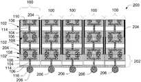
- FIG. 1is a cross-sectional profile view of example die-to-wafer and/or die-to-die stacking and molding, according to an embodiment.
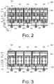
- FIG. 2is a cross-sectional profile view of example die-to-wafer and/or die-to-die stacking and molding, according to an embodiment wherein the top of the stacks is not covered.
- FIG. 3is a cross-sectional profile view of example die-to-wafer and/or die-to-die stacking and molding, according to an embodiment wherein the top of the stacks is covered.
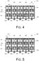
- FIG. 4is a cross-sectional profile view of example die-to-wafer and/or die-to-die stacking and molding, according to an embodiment wherein the top of the stacks is not covered and the molding extends to the bottom of the stack.
- FIG. 5is a cross-sectional profile view of example die-to-wafer and/or die-to-die stacking and molding, according to an embodiment wherein the top of the stacks is covered and the molding extends to the bottom of the stack.
- FIG. 6is a cross-sectional profile view of example die-to-wafer and/or die-to-die stacking and molding with unequal sized dies, according to an embodiment wherein the top of the stacks is covered.
- FIG. 7is a cross-sectional profile view of example die-to-wafer and/or die-to-die stacking and molding with unequal sized dies, according to an embodiment wherein the top of the stacks is covered and the molding extends to the bottom of the stack.
- FIG. 8is a cross-sectional profile view of example die-to-wafer and/or die-to-die stacking and molding, according to an embodiment wherein the top dies of the stacks do not have an interconnection on one side.
- FIG. 9is a cross-sectional profile view of example die-to-wafer and/or die-to-die stacking and molding, according to an embodiment wherein the top dies of the stacks do not have an interconnection on one side and the molding extends to the bottom of the stack.
- FIG. 10is a cross-sectional profile view of example die-to-wafer and/or die-to-die stacking and molding, including some lateral placement of dies on a single level, according to an embodiment.
- FIG. 11is a cross-sectional profile view of example die-to-wafer and/or die-to-die stacking and molding, including some lateral placement of dies and wafers on a single level, according to an embodiment.
- FIG. 12is a cross-sectional profile view of example die-to-wafer and/or die-to-die stacking including some etching of die edges, according to an embodiment.
- FIG. 13is a cross-sectional profile view of example die-to-wafer and/or die-to-die stacking and molding including some etching of die edges, according to an embodiment.
- FIG. 14is a cross-sectional profile view of example die-to-wafer and/or die-to-die hybrid bond stacking, including some etching of die edges, according to another embodiment.
- FIG. 15is a cross-sectional profile view of example die-to-wafer and/or die-to-die memory stacking, according to an embodiment.
- FIG. 16is a cross-sectional profile view of example die-to-wafer and/or die-to-die hybrid bond stacking, including flip chip terminations, according to an embodiment.
- FIGS. 17-20show cross-sectional profile views of example die-to-wafer and/or die-to-die hybrid bond stacking, including various combinations on a substrate, according to various embodiments.
- FIG. 21is a flow diagram illustrating an example process for forming a stacked and bonded structure, according to an embodiment.
- Representative techniques and devicesare disclosed, including process steps for stacking and bonding dies and/or wafers, including hybrid bonding dies to dies, dies to wafers, and wafers to wafers without adhesive.
- the dies and/or wafersare stacked and bonded in various arrangements including stacks, and may be covered with a molding to facilitate handling, packaging, and the like.
- the moldingmay cover more or less of a stack, to facilitate connectivity with the devices of the stack, to enhance thermal management, and so forth.
- circuitse.g., integrated circuits (IC), mixed circuits, ASICS, memory devices, processors, etc.
- groups of componentspassive elements, MEMS (Micro-Electro Mechanical Systems) components, packaged components, structures (e.g., wafers, panels, boards, PCBs, etc.), and the like, that may be integrated and coupled to interface with each other, with external circuits, systems, carriers, and the like.
- MEMSMicro-Electro Mechanical Systems
- microelectronic componentFor simplicity, unless otherwise specified, components being bonded to another component will be referred to herein as a “die.”
- FIG. 1is a cross-sectional profile view of example die-to-wafer and/or die-to-die stacking and molding, according to an embodiment.
- a stack 100(or microelectronic assembly 100 ) is formed by stacking and bonding (hybrid bonding without adhesive, for example) a plurality of dies 102 (e.g., any quantity of dies 102 desired).
- the stack 100is formed by stacking and bonding (hybrid bonding without adhesive, for example) a plurality of wafers, which are then singulated into the dies 102 shown in FIG. 1 .
- the dies 102may not be perfectly aligned in the stack 100 .
- the edges of the dies 102are not lined up exactly, and there is some error or misalignment “e” from one die 102 to another die 102 of the stack 100 .
- the misalignment “e”may be due to an accuracy tolerance of a pick and place tool, or the like.
- Dies 102may be formed using various techniques, to include a base substrate 104 and one or more insulating or dielectric layers 106 .
- the dies 102 shown at FIG. 1may represent double-sided dies 102 , having an insulating layer 106 on both surfaces of the base layer 104 .
- dies 102 ′may be single-sided or double-sided host dies or wafers.
- Single-sided dies 102 or 102 ′may be positioned in the stack 100 as the top die 102 , the bottom die 102 , or as any other die 102 in the stack 100 where direct-bond connectivity to both sides of the die 102 is not desired.
- the reference “die 102 ” as used hereinincludes both single and double-sided dies and wafers, unless otherwise specified.
- the base substrate 104may be comprised of silicon, germanium, glass, quartz, a dielectric surface, direct or indirect gap semiconductor materials or layers or another suitable material.
- the insulating layer 106is deposited or formed over the substrate 104 , and may be comprised of an inorganic dielectric material layer such as oxide, nitride, oxynitride, oxycarbide, carbides, carbonitrides, diamond, diamond like materials, glasses, ceramics, glass-ceramics, and the like.
- Bonding surfaces 108 of the die 102can include conductive features 110 , such as TSVs, traces, pads, and interconnect structures, for example, embedded into the insulating layer 106 and arranged so that the conductive features 110 from respective bonding surfaces 108 of opposing devices can be mated and joined during bonding, if desired.
- the joined conductive features 110can form continuous conductive interconnects (for signals, power, ground, etc.) between stacked devices.
- Damascene processesmay be used to form the embedded conductive features 110 in the insulating layer 106 .
- the conductive features 110may be comprised of metals (e.g., copper, etc.) or other conductive materials, or combinations of materials, and include structures, traces, pads, patterns, and so forth.
- a barrier layermay be deposited in the cavities for the conductive features 110 prior to depositing the material of the conductive features 110 , such that the barrier layer is disposed between the conductive features 110 and the insulating layer 106 .
- the barrier layermay be comprised of tantalum, titanium, tungsten layer or their combination with their various respective compounds or alloys, for example, or another conductive material, to prevent or reduce diffusion of the material of the conductive features 110 into the insulating layer 106 .
- the exposed surfaces of the device wafer 102including the insulating layer 106 and the conductive features 110 can be planarized (e.g., via CMP) to form the flat bonding surfaces 108 .
- Forming a bonding surface 108includes finishing the surface 108 to meet dielectric roughness specifications and metallic layer (e.g., copper, etc.) recess specifications (if specified), to prepare the surface 108 for hybrid bonding.
- the bonding surface 108is formed to be as flat and smooth as possible, with very minimal (nanometer scale) surface topology variance.
- Various conventional processessuch as chemical mechanical polishing (CMP), dry or wet etching, and so forth, may be used to achieve the low surface roughness. This process provides the flat, smooth surface 108 that results in a reliable bond.
- Embedded conductive traces 112that extend partially into the dielectric substrate 106 below the prepared surface 108 may be used to electrically couple the conductive features 110 to desired components throughout the die 102 .
- the conductive features 110may be coupled to conductive (e.g., copper) through-silicon vias (TSVs) 114 or the like, that extend partly or fully through the die 102 to make electrical connections through the thickness of the die 102 .
- TSVsthrough-silicon vias
- a TSV 114may extend about 50 microns in some cases, depending on the thickness of the die 102 .
- the figuresshow examples of dies 102 with various arrangements of conductive features 110 , traces 112 , and TSVs 114 that are not intended to be limiting.
- some of the conductive features 110 , traces 112 , and TSVs 114may not be present in a die 102 (or wafer) and in other embodiments, additional conductive features 110 , traces 112 , and TSVs 114 may be present, or other circuit components, and the like.
- Dies 102may be hybrid bonded, for instance, without adhesive to other dies 102 having metal pads 110 , traces 112 , and/or TSVs 114 , to make the desired electrical connections through the dies 102 while forming the stack 100 .
- Hybrid bondingincludes direct dielectric-to-dielectric bonding, without an adhesive or other intervening material, of the respective insulating layers 106 of each die 102 (e.g., ZIBOND®), as well as direct metal-to-metal bonding, also without an intervening material, of the respective conductive features 110 of each die 102 (e.g., DBI®).
- the dielectric-to-dielectric bondingoccurs spontaneously as the respective bonding surfaces 108 are brought together at ambient temperatures.
- the metal-to-metal bonding(which may include diffusion between the metal of the conductive features 10 ) can occur with the aid of heat, with or without pressure.
- electrical connectivitymay be established from the top surface of the top die 102 of the stack 100 (e.g., through conductive features 110 ), through the dies 102 (any number of dies 102 ) of the stack 100 (e.g., through conductive features 110 , traces 112 , and TSVs 114 ), and to the bottom surface of the bottom die 102 of the stack 100 (e.g., through a TSV 114 ).
- the top surface of the top die 102 of the stack 100e.g., through conductive features 110
- the dies 102any number of dies 102 of the stack 100
- TSVs 114any number of dies 102
- conductive features 110provides connectivity to the top surface of the stack 100 and a TSV 114 with at least one electrically coupled pad 116 provides connectivity to the bottom surface of the bottom die 102 of the stack 100 (in some cases, a titanium layer (not shown), or the like, may couple the TSV 114 to the pad 116 ).
- a titanium layer(not shown), or the like, may couple the TSV 114 to the pad 116 ).
- one or both of the top and bottom surfaces of the stack 100may not have connectivity or different components than shown may provide the connectivity to the top or bottom surfaces of the stack 100 .
- the stack 100may not include conductive features 110 at the top surface of the stack 100 or TSVs 114 in the top die 102 or TSVs 114 and pads 116 in the bottom die 102 .
- one or more of the TSVs 114provide thermal connectivity between the dies 102 .
- the TSVscan help to dissipate or transmit heat from some dies 102 to other dies 102 and/or to the outside environment.
- the TSVs 114are comprised of a thermally conductive material, and may include a thermally conductive barrier layer (not shown).
- the TSVs 114may be sized for optimal thermal dissipation, based on the function (e.g., heat generation) of the associated dies 102 .
- FIG. 2is a cross-sectional profile view of a microelectronic assembly 200 , comprising multiple stacks 100 of dies 102 .
- each stack 100includes the same quantity of dies 102 .
- some stacks 100may include a different quantity of dies 102 than other stacks 100 of the assembly 200 .
- the dies 102are not perfectly aligned in the stacks 100 .
- the edges of the dies 102are not lined up exactly within the stacks 100 , and there is some error or misalignment of the edges from die 102 to die 102 .
- the stacks 100are singulated from a plurality of wafers, which have been stacked and bonded as discussed above.
- the bottom set of dies 102 ′comprise a host wafer 202 for the stacks 100 .
- the dies 102can be stacked onto the host wafer 202 , which is then singulated at borders of the stacks 100 if desired.
- the host wafer 202may be singulated at a different stage in the process, if at all.
- one or more of the stacks 100 of the assembly 200may be covered in molding 204 comprising an encapsulant, or the like.
- the molding 204may comprise a high strength, high thermal stress (high heat resistant) encapsulant material, that may also have a high heat dissipation characteristic.
- CTEcoefficient of thermal expansion
- HITACHI®provides such an encapsulant or “epoxy molding compound,” referred to as “CEL.”
- Other like productsare also commercially available.
- the assembly 200is covered with the molding 204 , then the assembly 200 is diced into the multiple stacks 100 .
- the individual stacks 100may be covered with additional encapsulant 204 as desired.
- the stacks 100are molded after formation of the stacks 100 , including stacking and bonding individual dies 102 into the stacks 100 or singulation of wafers to form the dies 102 and stacks 100 .
- the molding 204may be deposited before or after singulation of the dies 102 .
- the molding 204can cover the entire stack 100 of dies 102 or selected dies 102 .
- the host wafer 202 (and the dies 102 ′)may not be covered with the molding 204 . This may be due to the manufacturing process or by design.
- the molding 204may be comprised of a single layer of encapsulant covering over and/or around some or all of the dies 102 of a stack 100 , or the molding 204 may be comprised of multiple layers (e.g., laminate) of encapsulant of the same or of different materials.
- the molding 204comprises particles within the encapsulant, and the molding 204 has a progression of density of the particles—from a state of low or no particles at the top or the bottom of the stack 100 to a state of higher density of particles at the other of the top or the bottom of the stack 100 .
- the particlesmay be present at different densities in multiple layers of encapsulant, when present.
- the molding 204comprises an inorganic casing, or the like.
- adding the molding 204 to the stacks 100 of dies 102 and/or to the assembly 200provides a final packaging to the stacks 100 or to the assembly 200 .
- the stack solutionallows ease of handling during processing and assembly, as well as for deployment in an application.
- the molding 204provides protection to the dies 102 and stacks 100 as well as the assembly 200 and any discrete components that may be packaged with the dies 102 .
- the top surface of one or more of the stacks 100may be free from molding 204 .
- the bare top surface of the top dies 102can be used for further interconnection of the top dies 102 of the stack 100 to other circuits, devices (e.g., optical, radio frequency (RF), analog, digital, logic, memory, or other devices), or the like (e.g., when conductive features 110 are present at the top surface of the top die 102 ), including additional dies 102 or assemblies 200 , for example.
- the top surface of the top dies 102may be uncovered to enhance thermal dissipation.
- heatmay dissipate from the dies 102 more readily and efficiently without the encapsulant 204 at the top surface of the top dies 102 of the assembly 200 .
- the conductive features 110(as well as the traces 112 ) may not be present at the top surface of the top dies 102 .
- the TSVs 114may be present if they are used to help dissipate heat through the top surface, for instance.
- the assembly 200includes one or more electrical contacts or terminals 206 at a surface (such as the bottom surface, for instance) of the assembly 200 .
- the terminals 206may be used for electrically coupling the assembly to another circuit, device, printed circuit board (PCB), or the like. As shown in FIG. 2 , the terminals 206 may be electrically coupled to the TSV 114 (or other interconnection) of the dies 102 (such as the bottom-most dies 102 ) of the stacks 100 of the assembly 200 through the pads 116 .
- the assembly 200may include electrical connectivity from the top dies 102 (e.g., the top surface of the top dies 102 in some cases) of one or more of the stacks 100 through the dies 102 of the stacks 100 , to the terminals 206 .
- the top dies 102e.g., the top surface of the top dies 102 in some cases
- TSVs 114may be optional in some dies 102 and/or in some stacks 100 in alternate implementations.
- the top surface of one or more of the stacks 100may include molding 204 .
- the molding 204 at the top surface of the stacks 100 and the assembly 200protects the stacks 100 and the assembly 200 during handling, assembly, deployment, and so forth.
- each of the stacks 100is individually covered with the molding 204 , including the top and sides of the stack 100 .
- the host wafer 202 (and the dies 102 ′)may not be covered with the molding 204 . As shown in the example of FIG.
- the top dies 102 of an assembly 200may not include conductive features 110 (or traces 112 and/or TSVs 114 ) when no electrical connections are to be made at the top surface of the dies 102 and the assembly 200 .
- These componentsmay be optional, for instance when they are used for other purposes (e.g., when circuit components are disposed on or within the upper insulating layer 106 , or the like).
- dies 102may have various configurations and arrangements of components in some applications.
- dies 102 ′′may include TSVs 114 that are coupled directly to conductive pads 110 on adjacent dies 102 to provide connectivity through to the adjacent bonded die 102 .
- an end surface of the TSV 114may be exposed at a bonding surface 108 of the die 102 ′′, forming a contact surface for bonding to a conductive pad 110 on an adjacent die 102 .
- the dies 102 ′′may include conductive pads 110 at a bonding surface, with a TSV 114 directly coupled to the conductive pad 110 . These conductive pads 110 may be bonded to the conductive pads 110 (or other conductive structures) on an adjacent die 102 .
- the entire stacks 100may be covered with the molding 204 , including the host wafer 202 and dies 102 ′.
- the host wafer 202may be singulated into dies 102 ′ prior to the encapsulating step, facilitating their being covered by molding 204 .
- Multiple dies 102may be stacked (in groups or one at a time) onto a host die 102 ′ to form a stack 100 , which may then be covered with the molding 204 .
- the molding 204may be applied to the assembly 200 after all of the dies 102 are stacked and bonded into stacks 100 . Molding 204 can be present on the sides of the stacks 100 in any case. Further, the stacks 100 of the assembly 200 may be separated from each other after the molding step in alternate embodiments.
- FIG. 4illustrates an example assembly 200 where the top surface (i.e, back) of the assembly 200 and the stacks 100 is free from molding 204 .
- the molding 204may be deposited over the assembly 200 , and then removed from the top surface of the stacks 100 .
- the molding 204may be removed from the top surface of the stacks 100 to provide for interconnection to the top dies 102 , for improved thermal dissipation, or the like.
- FIG. 5illustrates the case where the top surface (i.e., back) is covered with the molding 204 .
- the dies 102 of the stacks 100may not be uniform in size (e.g., dimensions, area, footprint, thickness, etc.). Dies 102 with different footprints or thicknesses, for example, may be stacked and bonded to form the stacks 100 . Without the molding 204 , the stack 100 of non-uniform dies 102 presents uneven side edges and/or stacks 100 of different heights. Covering the stacks 100 with molding 204 can present a uniform package (in side edges/surfaces as well as height) as stacks 100 and/or an assembly 200 .
- the example illustrated at FIG. 6shows an embodiment where the dies 102 are covered with the molding 204 , but the host wafer (host dies 102 ′) is not covered with the molding 204 .
- the thickness of the mold layer 204 on the side edges of the top die 102is thicker than the thickness of the mold layer 204 disposed on the side edges of the second die 102 beneath.
- FIG. 7shows an embodiment where the dies 102 and the host dies 102 ′ are all covered with the molding 204 , as discussed above.
- the stacks 100may include dies 102 with interconnections on one side and not the other.
- the top dies 102may not have interconnections to the top surface of the die 102 . In such cases, no interconnection may be desired on the top (e.g., back) surface of the stacks 100 or assembly 200 .
- other dies 102may include interconnections on one side only.
- the TSV 114is also optional for the top die 102 , however, the TSV 114 may be used for thermal dissipation.
- a heat sink 802 or other component 902may be included in a stack 100 .
- a heat sink 802may be located at the top of the stack 100 to assist in dissipating heat from one or more dies 102 of the stack 100 into the environment.
- thermally conductive TSVs 114may help to transport excess heat from some dies 102 to other dies 102 and to the heat sink 802 .
- the heat sink 802 or other component 902may be located somewhere within the stack 100 or at the bottom of the stack 100 as desired for its application and performance.
- the top of the stack 100(e.g., the top or “back” surface of the die 102 ) may be free from molding 204 .
- some of the stacks 100 of an assembly 200may include molding 204 all around the stack 100 and including at the top surface of the stack 100 , while other stacks 100 (for instance stacks 100 that include a heat sink 802 or other component 902 ) may be free of molding 204 at the top surface, while having molding 204 at the sides of the stack 100 .
- uniform and/or non-uniform dies 102may be stacked and bonded to form stacks 100 , where multiple dies 102 are placed laterally on a single level within the assembly 200 package.
- the host wafer 202may not be singulated at each of the stacks 100 . Consequently, more than one stack 100 may be bonded to a single host die 102 ′.
- the second and third stacks 100are bonded to a single host die 102 ′ and the fourth and fifth stacks 100 are bonded to another host die 102 ′.
- the groups of stacks 100 bonded to a host die 102 ′may be covered in molding 204 together.
- the second and third stacks 100may be covered in molding 204 together (e.g., commonly encapsulated) and the fourth and fifth stacks 100 may be covered in molding 204 together (e.g., commonly encapsulated).
- the molding 204 of some groups of stacks 100 bonded to a common host die 102 ′may be separated, with separate molding 204 around each stack 100 individually.
- the host dies 102 ′ (or wafer)may be free from molding, as shown in the example. Alternately, the host dies 102 ′ (or wafer) may be covered with molding 204 .
- additional dies 102may be stacked in a lateral arrangement on a single level of the assembly 200 , forming one or more common stacks or partially common stacks 1100 .
- FIG. 11shows an example of partially common stacks 1100 .
- the first row of dies 102 that are bonded to the host dies 102 ′may not be singulated at each of the stacks 100 . Consequently, more than one stack 100 may be bonded to a single host die 102 ′ and a single “first row” die 102 .
- the second and third stacks 100comprise a single first row die 102 bonded to a single host die 102 ′.
- the subsequent rows of dies 102 of the second and third stacks 100are bonded to the single first row die 102 .
- the second and third stacks 100share a common host die 102 ′ and a common first row die 102 .
- additional rows of dies 102may be common to the second and third stacks 100 . For example, if the dies 102 of all rows of multiple stacks 100 are common to the multiple stacks 100 , this would result in a common stack 1100 .
- the fourth and fifth stacks 100also comprise a single first row die 102 bonded to a single host die 102 ′.
- the subsequent rows of dies 102 of the fourth and fifth stacks 100are bonded to the single first row die 102 . Accordingly, the fourth and fifth stacks 100 share a common host die 102 ′ and a common first row die 102 , resulting in a partially common stack 1100 .
- the first stack 100is covered with molding 204 (except for the host die 102 ′), and each of the partially common stacks 1100 are also covered with molding 204 (except for the host die 102 ′).
- one or more partially common stacks 1100may include molding 204 at the top surface of the dies 102 of the partially common stack 1100 and one or more partially common stacks 1100 may be free of molding 204 at the top surface of the dies 102 of the partially common stack 1100 .
- removing the molding 204 (or not depositing the molding 204 ) at the top surface of the top dies 102can allow interconnectivity with the top dies 102 , can allow for improved heat dissipation from the top dies 102 , and so forth.
- FIGS. 12 and 13illustrate example embodiments of an assembly 200 where one or more stacks 100 of bonded dies 102 are bonded to a host wafer 202 .
- the host wafer 202may be singulated into host dies 102 ′ (not shown).
- the dies 102may be double-sided dies with conductive features 110 embedded within insulating layers 106 on either side of a base layer 104 .
- Some details, such as traces 112 and TSVs 114can be assumed to be present in some embodiments, but are not illustrated, for clarity of the figures.
- one or more of the insulating layers 106may be etched (see 1202 ) at the perimeter edge of the dies 102 , removing some of the insulating layer 106 at the perimeter.
- the perimeter etching 1202may be intentional, based on a specification for the device, the package, the processing, or the like.
- the etching 1202may be present on one or more sides or edges of the dies 102 .
- the etching 1202comprises removal of a portion of the insulating layer 106 at the perimeter and exposing the base layer 104 below. In other cases, the etching 1202 does not expose the base layer 104 or the etching 1202 also removes some of the base layer 104 as well.
- FIG. 14is an additional illustration of dies 102 with etched perimeter edges (recesses 1202 ), according to an embodiment.
- the illustration of FIG. 14more closely shows the relative scale of the recesses 1202 with respect to the base layer 104 and the insulating layers 106 , in an example embodiment. In other embodiments, other proportions may be present.
- molding 204 compoundmay be filled with particles, as discussed above.
- the particlesmay be added to the molding 204 to change a coefficient of thermal expansion (CTE) of the molding 204 . This can assist in reducing package warpage, for instance, by balancing the CTE across the package (e.g., assembly 200 ).
- CTEcoefficient of thermal expansion
- the particles in the molding 204may be too large to fit within the smaller recesses 1202 formed by the perimeter etching. Any voids left behind after the molding 204 is applied to the stacks 100 could cause “popcorn” failure in assembly of the package (e.g., assembly 200 ).
- multiple layers of molding 204may be used to mitigate possible failures.
- a first low viscosity compound 1302may be applied around the stacks 100 , forming a layer of compound 1302 around the stacks 100 and penetrating the etched recesses 1202 .
- the layer 1302can then be followed by a layer of the molding 204 .
- the first layer compound 1302may not include a filler or particles.
- the primary purpose of the compound 1302may be to fill the etched recesses 1302 in the dies 102 .
- the compound 1302may also form a layer over the vertical wall of the dies 102 of the stack 100 .
- the stacks 100 and/or the assembly 200may be covered with the molding 204 .
- additional layersmay also be used to cover the stacks 100 and/or the assembly 200 .
- the first layer (low viscosity) compound 1302may include sub-micron particles or even nano particles sufficiently small to be incorporated within the recess 1202 .
- the sub-micron or nano particlesmay be comprised of silica, silicon, a silica/silicon compound, or the like. Nano particles may average 20 nm in size (e.g., diameter) in some cases, and may be smaller or larger in other cases.
- the first layer compound 1302(with sub-micron or nano-sized filler particles) forms a layer over the vertical wall of dies 102 and the recess 1202 .
- the sub-micron or nanoparticles content of the first layer compound 1302be more than 5%.
- the molding layer 204typically comprises reinforcing particulate with a particulate content typically greater than 50%, and it may be preferable that the particulate content of the mold layer 204 be higher than the particulate content of the first layer compound 1302 within the recess 1202 .
- the nominal size of the particulates in the mold layer 204be larger than the nominal size of the particulates in the first layer compound 1302 .
- memory diesare coupled to other memory dies using ball-grid arrays (BGA) and other similar technologies.
- BGAball-grid arrays
- memory die to memory die pitchis often about 45 microns.
- logic die to interposer pitchis about 90-100 microns.
- FIGS. 15 and 16show examples of a “high bandwidth memory” assembly 200 , including a stack 100 of memory dies 102 (e.g., dynamic random access memory (DRAM), static random access memory (SRAM), flash memory, etc.) coupled to a logic die 1502 .
- the dies 102are hybrid bonded (DBI®) to form the stack 100 , as discussed above.
- the stack 100(or the bottom die 102 ) may be hybrid bonded to the logic die 1502 .
- the logic die 1502may include terminals 206 for coupling the assembly 200 to a circuit, PCB, device, or the like, as discussed above.
- circuit elements(such as conductive features 110 , or the like) at the bonding surface of one or more of the bonded dies 102 is less than 20 microns and in other applications less than 5 microns or even less than 1 micron.
- the stack 100may alternately be coupled to the logic die 1502 using flip-chip technology, or the like.
- flip-chip terminals 1602may be coupled to the bottom side of the bottom die 102 , which interface with terminals 1602 at the top surface of the logic die 1502 .
- a combination of hybrid bonding and flip-chip technologymay be used with the assembly 200 .
- other coupling technologiesmay also be used to couple a hybrid bonded stack 100 to a logic die 1502 , an interposer, or the like, if desired.
- a molding 1604which covers the flip-chip terminals 1602 and fills in the gap between the stack 100 and the logic die 1502 .
- the assembly 200may also be covered with a molding 204 , if desired for handling, packaging, and so forth.
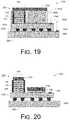
- FIGS. 17-20show additional implementations that use a stack 100 and/or an assembly 200 in various applications.
- an assembly 1700is shown that includes various dies 102 , including a stack 100 of dies 102 , hybrid bonded to an interposer 1702 .
- the interposer 1702is comprised of a semiconductor such as silicon, for example. The drawing is simplified for clarity.
- some dies 102may be molded and other dies 102 may not be molded.
- a heat sink or other cooling device 1704e.g., fan, etc.
- the interposer 1702includes hybrid bonding pads 110 as well as at least one wirebond pad 1706 .
- a wirebond pad 1706may be used to couple a remote component (for instance a component coupled to (or through) or integral to the laminate 1802 ) to the pad 1706 via a wire 1804 .
- the laminate 1802is hybrid bonded to the interposer 1702 .
- the laminate 1802may be coupled to the interposer 1702 with another bonding technology.
- the laminate 1802may be coupled to the interposer 1702 with BGA technology, another surface-mount technology, or the like.
- the laminate 1802may include one or more wirebond pads 1902 , which may be used with a wire 1804 to couple to a wirebond pad 1706 , or the like.
- the assembly 200 or the stack 100may be packaged with another component 1904 , which may be hybrid bonded to the interposer 1702 .
- the component 1904 and the assembly 200 or the stack 100may be covered in a molding 1906 , comprising an encapsulant (or other package) if desired.
- the package or the stack 100 and component 1904may be hybrid bonded to the interposer 1702 .
- a cooling device 1704may be coupled to the component 1904 and/or the stack 100 , as shown in FIG. 19 .
- a fill 1604may be used to cover the terminals 206 and fill in the gap between the interposer 1702 and the laminate 1802 .
- the interposer 1702may be encapsulated, either with other components or separately.
- the stack 100may be covered with molding 204 , and other dies 102 and/or components may not.
- a heat sink or other cooling device 1704e.g., fan, etc.
- An additional cooling devicemay also be coupled to the stack 100 , which may be free of molding 204 at the top surface of the stack 100 .
- the interposer 1702includes hybrid bonding pads 110 as well as at least one wirebond pad 1706 . As shown, the interposer 1702 may be coupled to the laminate 1802 via a BGA arrangement, or other coupling technology.
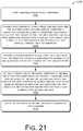
- FIG. 21is a flow diagram illustrating an example process 2100 of forming a stacked and bonded microelectronic assembly (such as the microelectronic assembly 200 ) comprising a stack of dies (such as stack 100 of dies 102 , for example).
- the stack of diesmay be covered with a molding (such as molding 204 , for example) for handling, processing, application, and the like.
- the process 2100refers to FIGS. 1-20 .
- the processincludes forming a microelectronic stack (such as stack 100 of dies 102 , for example).
- the processcomprises forming a plurality of the microelectronic stacks.
- forming the microelectronic stackincludes the following blocks:
- the processincludes providing a first substrate (such as a first die 102 , for example) having a front side and a back side.
- the back sidehaving a bonding surface comprising a nonconductive bonding layer and an exposed electrically conductive first circuit element.
- the first substratehaving a first conductive via electrically coupled to the first circuit element of the first substrate and extending at least partially through the first substrate.
- the processincludes providing a second substrate having a front side and a back side.
- the front sideincluding a nonconductive bonding layer and an exposed electrically conductive first circuit element.
- the processincludes coupling the front side of the second substrate to the back side of the first substrate by contacting the nonconductive bonding layers of the first and second substrates.
- side edges of the first substrateare misaligned relative to side edges of the second substrate.
- the couplingincludes contacting the first circuit element of the first substrate to the first circuit element of the second substrate (e.g., hybrid bonding).
- the processincludes covering the side edges of the first and second substrates with a molding (such as molding 204 , for example).
- a moldingsuch as molding 204 , for example.
- the processincludes covering the back side of the second substrate with the molding.
- the moldingincludes more than one layer or more than one material or compound.
- at least one of a plurality of layers of the moldingincludes particles to assist in balancing the CTE of the assembly, to avoid warpage of the assembly.
- the back side of the second substrateincludes a second nonconductive bonding layer and an exposed electrically conductive second circuit element.
- the second substratehas a second conductive via electrically coupling the first and second circuit elements of the second substrate.
- the processincludes providing a third substrate having a front side and a back side, the front side including a nonconductive bonding layer and an exposed electrically conductive first circuit element.
- the processincludes coupling the front side of the third substrate to the back side of the second substrate by contacting the nonconductive bonding layer of the third substrate to the nonconductive bonding layer of the second substrate.
- side edges of the third substrateare misaligned relative to side edges of the second and/or first substrates.
- the couplingincludes contacting the first circuit element of the third substrate to the second circuit element of the second substrate (e.g., hybrid bonding).
- the processincludes forming a recess at the bonding layer of the first and/or the second substrates at a perimeter of the first and/or the second substrates and filling at least the recess with a low viscosity compound prior to covering the side edges of the first and second substrates with the molding.
- the processincludes covering the side edges of the third substrate with the molding. In a further implementation, the process includes covering the back side of the third substrate with the molding.
- the processincludes hybrid bonding the microelectronic stack to a semiconductor interposer having at least one wirebond contact pad.
- the processincludes coupling the interposer to a laminate having a second wirebond contact pad and bonding the at least one wirebond contact pad of the interposer to the second wirebond contact pad of the laminate with a wire.
- the interposermay be hybrid bonded to the laminate.
- various portions of the microelectronic assemblyare covered with one or more layers of molding, while other portions are not.
Landscapes
- Engineering & Computer Science (AREA)
- Microelectronics & Electronic Packaging (AREA)
- Power Engineering (AREA)
- Computer Hardware Design (AREA)
- Physics & Mathematics (AREA)
- Condensed Matter Physics & Semiconductors (AREA)
- General Physics & Mathematics (AREA)
- Manufacturing & Machinery (AREA)
- Geometry (AREA)
- Structures Or Materials For Encapsulating Or Coating Semiconductor Devices Or Solid State Devices (AREA)
- Internal Circuitry In Semiconductor Integrated Circuit Devices (AREA)
- Casting Or Compression Moulding Of Plastics Or The Like (AREA)
Abstract
Description
Claims (35)
Priority Applications (8)
| Application Number | Priority Date | Filing Date | Title |
|---|---|---|---|
| PCT/US2019/040391WO2020010136A1 (en) | 2018-07-06 | 2019-07-02 | Molded direct bonded and interconnected stack |
| US16/460,068US11158606B2 (en) | 2018-07-06 | 2019-07-02 | Molded direct bonded and interconnected stack |
| TW108123487ATWI834682B (en) | 2018-07-06 | 2019-07-03 | Molded direct bonded and interconnected stack |
| TW113104743ATW202427685A (en) | 2018-07-06 | 2019-07-03 | Molded direct bonded and interconnected stack |
| US17/448,794US11764189B2 (en) | 2018-07-06 | 2021-09-24 | Molded direct bonded and interconnected stack |
| US18/148,327US11837582B2 (en) | 2018-07-06 | 2022-12-29 | Molded direct bonded and interconnected stack |
| US18/513,431US12266640B2 (en) | 2018-07-06 | 2023-11-17 | Molded direct bonded and interconnected stack |
| US19/068,370US20250246583A1 (en) | 2018-07-06 | 2025-03-03 | Molded direct bonded and interconnected stack |
Applications Claiming Priority (2)
| Application Number | Priority Date | Filing Date | Title |
|---|---|---|---|
| US201862694845P | 2018-07-06 | 2018-07-06 | |
| US16/460,068US11158606B2 (en) | 2018-07-06 | 2019-07-02 | Molded direct bonded and interconnected stack |
Related Child Applications (1)
| Application Number | Title | Priority Date | Filing Date |
|---|---|---|---|
| US17/448,794ContinuationUS11764189B2 (en) | 2018-07-06 | 2021-09-24 | Molded direct bonded and interconnected stack |
Publications (2)
| Publication Number | Publication Date |
|---|---|
| US20200013754A1 US20200013754A1 (en) | 2020-01-09 |
| US11158606B2true US11158606B2 (en) | 2021-10-26 |
Family
ID=69060191
Family Applications (5)
| Application Number | Title | Priority Date | Filing Date |
|---|---|---|---|
| US16/460,068Active2039-10-06US11158606B2 (en) | 2018-07-06 | 2019-07-02 | Molded direct bonded and interconnected stack |
| US17/448,794ActiveUS11764189B2 (en) | 2018-07-06 | 2021-09-24 | Molded direct bonded and interconnected stack |
| US18/148,327ActiveUS11837582B2 (en) | 2018-07-06 | 2022-12-29 | Molded direct bonded and interconnected stack |
| US18/513,431ActiveUS12266640B2 (en) | 2018-07-06 | 2023-11-17 | Molded direct bonded and interconnected stack |
| US19/068,370PendingUS20250246583A1 (en) | 2018-07-06 | 2025-03-03 | Molded direct bonded and interconnected stack |
Family Applications After (4)
| Application Number | Title | Priority Date | Filing Date |
|---|---|---|---|
| US17/448,794ActiveUS11764189B2 (en) | 2018-07-06 | 2021-09-24 | Molded direct bonded and interconnected stack |
| US18/148,327ActiveUS11837582B2 (en) | 2018-07-06 | 2022-12-29 | Molded direct bonded and interconnected stack |
| US18/513,431ActiveUS12266640B2 (en) | 2018-07-06 | 2023-11-17 | Molded direct bonded and interconnected stack |
| US19/068,370PendingUS20250246583A1 (en) | 2018-07-06 | 2025-03-03 | Molded direct bonded and interconnected stack |
Country Status (3)
| Country | Link |
|---|---|
| US (5) | US11158606B2 (en) |
| TW (2) | TW202427685A (en) |
| WO (1) | WO2020010136A1 (en) |
Cited By (82)
| Publication number | Priority date | Publication date | Assignee | Title |
|---|---|---|---|---|
| US20210297057A1 (en)* | 2018-12-21 | 2021-09-23 | Murata Manufacturing Co., Ltd. | Method for manufacturing electronic component module and electronic component module |
| US20220020729A1 (en)* | 2018-07-06 | 2022-01-20 | Invensas Bonding Technologies, Inc. | Molded direct bonded and interconnected stack |
| US11462419B2 (en) | 2018-07-06 | 2022-10-04 | Invensas Bonding Technologies, Inc. | Microelectronic assemblies |
| US11476213B2 (en) | 2019-01-14 | 2022-10-18 | Invensas Bonding Technologies, Inc. | Bonded structures without intervening adhesive |
| US11515202B2 (en) | 2005-08-11 | 2022-11-29 | Adeia Semiconductor Bonding Technologies Inc. | 3D IC method and device |
| US11515279B2 (en) | 2018-04-11 | 2022-11-29 | Adeia Semiconductor Bonding Technologies Inc. | Low temperature bonded structures |
| US11538781B2 (en) | 2020-06-30 | 2022-12-27 | Adeia Semiconductor Bonding Technologies Inc. | Integrated device packages including bonded structures |
| US11552041B2 (en) | 2017-09-24 | 2023-01-10 | Adeia Semiconductor Bonding Technologies Inc. | Chemical mechanical polishing for hybrid bonding |
| US11600542B2 (en) | 2017-12-22 | 2023-03-07 | Adeia Semiconductor Bonding Technologies Inc. | Cavity packages |
| US11610846B2 (en) | 2019-04-12 | 2023-03-21 | Adeia Semiconductor Bonding Technologies Inc. | Protective elements for bonded structures including an obstructive element |
| US11621246B2 (en) | 2019-03-29 | 2023-04-04 | Adeia Semiconductor Technologies Llc | Diffused bitline replacement in stacked wafer memory |
| US11626363B2 (en) | 2016-12-29 | 2023-04-11 | Adeia Semiconductor Bonding Technologies Inc. | Bonded structures with integrated passive component |
| US11631586B2 (en) | 2012-08-30 | 2023-04-18 | Adeia Semiconductor Bonding Technologies Inc. | Heterogeneous annealing method |
| US20230145518A1 (en)* | 2021-11-05 | 2023-05-11 | Nanya Technology Corporation | Die bonding structure, stack structure, and method of forming die bonding structure |
| US11652083B2 (en) | 2017-05-11 | 2023-05-16 | Adeia Semiconductor Bonding Technologies Inc. | Processed stacked dies |
| US11658173B2 (en) | 2016-05-19 | 2023-05-23 | Adeia Semiconductor Bonding Technologies Inc. | Stacked dies and methods for forming bonded structures |
| US11664357B2 (en) | 2018-07-03 | 2023-05-30 | Adeia Semiconductor Bonding Technologies Inc. | Techniques for joining dissimilar materials in microelectronics |
| US11670615B2 (en) | 2016-12-21 | 2023-06-06 | Adeia Semiconductor Bonding Technologies Inc. | Bonded structures |
| US11694925B2 (en) | 2017-10-06 | 2023-07-04 | Adeia Semiconductor Bonding Technologies Inc. | Diffusion barrier collar for interconnects |
| US11710718B2 (en) | 2015-07-10 | 2023-07-25 | Adeia Semiconductor Technologies Llc | Structures and methods for low temperature bonding using nanoparticles |
| US11715730B2 (en) | 2017-03-16 | 2023-08-01 | Adeia Semiconductor Technologies Llc | Direct-bonded LED arrays including optical elements configured to transmit optical signals from LED elements |
| US11721653B2 (en) | 2019-12-23 | 2023-08-08 | Adeia Semiconductor Bonding Technologies Inc. | Circuitry for electrical redundancy in bonded structures |
| US11728273B2 (en) | 2020-09-04 | 2023-08-15 | Adeia Semiconductor Bonding Technologies Inc. | Bonded structure with interconnect structure |
| US11728287B2 (en) | 2019-04-12 | 2023-08-15 | Adeia Semiconductor Bonding Technologies Inc. | Wafer-level bonding of obstructive elements |
| US11728313B2 (en) | 2018-06-13 | 2023-08-15 | Adeia Semiconductor Bonding Technologies Inc. | Offset pads over TSV |
| US11735523B2 (en) | 2020-05-19 | 2023-08-22 | Adeia Semiconductor Bonding Technologies Inc. | Laterally unconfined structure |
| US11742315B2 (en) | 2017-04-21 | 2023-08-29 | Adeia Semiconductor Bonding Technologies Inc. | Die processing |
| US11742314B2 (en) | 2020-03-31 | 2023-08-29 | Adeia Semiconductor Bonding Technologies Inc. | Reliable hybrid bonded apparatus |
| US11756880B2 (en) | 2018-10-22 | 2023-09-12 | Adeia Semiconductor Bonding Technologies Inc. | Interconnect structures |
| US11764177B2 (en) | 2020-09-04 | 2023-09-19 | Adeia Semiconductor Bonding Technologies Inc. | Bonded structure with interconnect structure |
| US11760059B2 (en) | 2003-05-19 | 2023-09-19 | Adeia Semiconductor Bonding Technologies Inc. | Method of room temperature covalent bonding |
| US11762200B2 (en) | 2019-12-17 | 2023-09-19 | Adeia Semiconductor Bonding Technologies Inc. | Bonded optical devices |
| US11790219B2 (en) | 2017-08-03 | 2023-10-17 | Adeia Semiconductor Inc. | Three dimensional circuit implementing machine trained network |
| US11791307B2 (en) | 2018-04-20 | 2023-10-17 | Adeia Semiconductor Bonding Technologies Inc. | DBI to SI bonding for simplified handle wafer |
| US11804377B2 (en) | 2018-04-05 | 2023-10-31 | Adeia Semiconductor Bonding Technologies, Inc. | Method for preparing a surface for direct-bonding |
| US20230387082A1 (en)* | 2019-05-30 | 2023-11-30 | Taiwan Semiconductor Manufacturing Co., Ltd. | System Formed Through Package-In-Package Formation |
| US11842894B2 (en) | 2019-12-23 | 2023-12-12 | Adeia Semiconductor Bonding Technologies Inc. | Electrical redundancy for bonded structures |
| US11848284B2 (en) | 2019-04-12 | 2023-12-19 | Adeia Semiconductor Bonding Technologies Inc. | Protective elements for bonded structures |
| US11855064B2 (en) | 2018-02-15 | 2023-12-26 | Adeia Semiconductor Bonding Technologies Inc. | Techniques for processing devices |
| US11862604B2 (en) | 2018-06-22 | 2024-01-02 | Adeia Semiconductor Inc. | Systems and methods for releveled bump planes for chiplets |
| US11860415B2 (en) | 2018-02-26 | 2024-01-02 | Adeia Semiconductor Bonding Technologies Inc. | Integrated optical waveguides, direct-bonded waveguide interface joints, optical routing and interconnects |
| US11862602B2 (en) | 2019-11-07 | 2024-01-02 | Adeia Semiconductor Technologies Llc | Scalable architecture for reduced cycles across SOC |
| US11876076B2 (en) | 2019-12-20 | 2024-01-16 | Adeia Semiconductor Technologies Llc | Apparatus for non-volatile random access memory stacks |
| US11881454B2 (en) | 2016-10-07 | 2024-01-23 | Adeia Semiconductor Inc. | Stacked IC structure with orthogonal interconnect layers |
| US11894326B2 (en) | 2017-03-17 | 2024-02-06 | Adeia Semiconductor Bonding Technologies Inc. | Multi-metal contact structure |
| US11894345B2 (en) | 2018-08-28 | 2024-02-06 | Adeia Semiconductor Inc. | Integrated voltage regulator and passive components |
| US11901281B2 (en) | 2019-03-11 | 2024-02-13 | Adeia Semiconductor Bonding Technologies Inc. | Bonded structures with integrated passive component |
| US11908739B2 (en) | 2017-06-05 | 2024-02-20 | Adeia Semiconductor Technologies Llc | Flat metal features for microelectronics applications |
| US11916054B2 (en) | 2018-05-15 | 2024-02-27 | Adeia Semiconductor Bonding Technologies Inc. | Stacked devices and methods of fabrication |
| US11929347B2 (en) | 2020-10-20 | 2024-03-12 | Adeia Semiconductor Technologies Llc | Mixed exposure for large die |
| US11948847B2 (en) | 2017-12-22 | 2024-04-02 | Adeia Semiconductor Bonding Technologies Inc. | Bonded structures |
| US11955393B2 (en) | 2018-05-14 | 2024-04-09 | Adeia Semiconductor Bonding Technologies Inc. | Structures for bonding elements including conductive interface features |
| US11955445B2 (en) | 2018-06-13 | 2024-04-09 | Adeia Semiconductor Bonding Technologies Inc. | Metal pads over TSV |
| US11955463B2 (en) | 2019-06-26 | 2024-04-09 | Adeia Semiconductor Bonding Technologies Inc. | Direct bonded stack structures for increased reliability and improved yield in microelectronics |
| US11967575B2 (en) | 2018-08-29 | 2024-04-23 | Adeia Semiconductor Bonding Technologies Inc. | Bond enhancement structure in microelectronics for trapping contaminants during direct-bonding processes |
| US11973056B2 (en) | 2016-10-27 | 2024-04-30 | Adeia Semiconductor Technologies Llc | Methods for low temperature bonding using nanoparticles |
| US11978681B2 (en) | 2019-04-22 | 2024-05-07 | Adeia Semiconductor Bonding Technologies Inc. | Mitigating surface damage of probe pads in preparation for direct bonding of a substrate |
| US12009338B2 (en) | 2020-03-19 | 2024-06-11 | Adeia Semiconductor Bonding Technologies Inc. | Dimension compensation control for directly bonded structures |
| US12051621B2 (en) | 2016-12-28 | 2024-07-30 | Adeia Semiconductor Bonding Technologies Inc. | Microelectronic assembly from processed substrate |
| US12074092B2 (en) | 2018-05-30 | 2024-08-27 | Adeia Semiconductor Inc. | Hard IP blocks with physically bidirectional passageways |
| US12080672B2 (en) | 2019-09-26 | 2024-09-03 | Adeia Semiconductor Bonding Technologies Inc. | Direct gang bonding methods including directly bonding first element to second element to form bonded structure without adhesive |
| US12100676B2 (en) | 2018-04-11 | 2024-09-24 | Adeia Semiconductor Bonding Technologies Inc. | Low temperature bonded structures |
| US12113054B2 (en) | 2019-10-21 | 2024-10-08 | Adeia Semiconductor Technologies Llc | Non-volatile dynamic random access memory |
| US12136605B2 (en) | 2018-08-31 | 2024-11-05 | Adeia Semiconductor Bonding Technologies Inc. | Layer structures for making direct metal-to-metal bonds at low temperatures in microelectronics and method for forming the same |
| US12142528B2 (en) | 2016-10-07 | 2024-11-12 | Adeia Semiconductor Inc. | 3D chip with shared clock distribution network |
| US12154880B2 (en) | 2018-12-18 | 2024-11-26 | Adeia Semiconductor Bonding Technologies Inc. | Method and structures for low temperature device bonding |
| US12174246B2 (en) | 2019-05-23 | 2024-12-24 | Adeia Semiconductor Bonding Technologies Inc. | Security circuitry for bonded structures |
| US12191267B2 (en) | 2019-03-01 | 2025-01-07 | Adeia Semiconductor Technologies, LLC | Nanowire bonding interconnect for fine-pitch microelectronics |
| US12211809B2 (en) | 2020-12-30 | 2025-01-28 | Adeia Semiconductor Bonding Technologies Inc. | Structure with conductive feature and method of forming same |
| US12255163B2 (en) | 2021-08-12 | 2025-03-18 | Micron Technology, Inc. | Bond pads for semiconductor die assemblies and associated methods and systems |
| US12270970B2 (en) | 2018-03-20 | 2025-04-08 | Adeia Semiconductor Bonding Technologies Inc. | Direct-bonded lamination for improved image clarity in optical devices |
| US12272730B2 (en) | 2018-03-29 | 2025-04-08 | Adeia Semiconductor Inc. | Transistor level interconnection methodologies utilizing 3D interconnects |
| US12300634B2 (en) | 2021-08-02 | 2025-05-13 | Adeia Semiconductor Bonding Technologies Inc. | Protective semiconductor elements for bonded structures |
| US12322667B2 (en) | 2017-03-21 | 2025-06-03 | Adeia Semiconductor Bonding Technologies Inc. | Seal for microelectronic assembly |
| US12341083B2 (en) | 2023-02-08 | 2025-06-24 | Adeia Semiconductor Bonding Technologies Inc. | Electronic device cooling structures bonded to semiconductor elements |
| US12374656B2 (en) | 2017-06-15 | 2025-07-29 | Adeia Semiconductor Bonding Technologies Inc. | Multi-chip modules formed using wafer-level processing of a reconstituted wafer |
| US12374556B2 (en) | 2016-12-28 | 2025-07-29 | Adeia Semiconductor Bonding Technologies Inc. | Processing stacked substrates |
| US12374641B2 (en) | 2019-06-12 | 2025-07-29 | Adeia Semiconductor Bonding Technologies Inc. | Sealed bonded structures and methods for forming the same |
| US12381128B2 (en) | 2020-12-28 | 2025-08-05 | Adeia Semiconductor Bonding Technologies Inc. | Structures with through-substrate vias and methods for forming the same |
| US12381168B2 (en) | 2015-08-25 | 2025-08-05 | Adeia Semiconductor Bonding Technologies Inc. | Conductive barrier direct hybrid bonding |
| US12406959B2 (en) | 2018-07-26 | 2025-09-02 | Adeia Semiconductor Bonding Technologies Inc. | Post CMP processing for hybrid bonding |
| US12424584B2 (en) | 2020-10-29 | 2025-09-23 | Adeia Semiconductor Bonding Technologies Inc. | Direct bonding methods and structures |
Families Citing this family (41)
| Publication number | Priority date | Publication date | Assignee | Title |
|---|---|---|---|---|
| CN108288616B (en) | 2016-12-14 | 2023-04-07 | 成真股份有限公司 | Chip package |
| WO2018186198A1 (en)* | 2017-04-04 | 2018-10-11 | ソニーセミコンダクタソリューションズ株式会社 | Solid state imaging device and electronic apparatus |
| US10447274B2 (en) | 2017-07-11 | 2019-10-15 | iCometrue Company Ltd. | Logic drive based on standard commodity FPGA IC chips using non-volatile memory cells |
| US10957679B2 (en) | 2017-08-08 | 2021-03-23 | iCometrue Company Ltd. | Logic drive based on standardized commodity programmable logic semiconductor IC chips |
| US10630296B2 (en) | 2017-09-12 | 2020-04-21 | iCometrue Company Ltd. | Logic drive with brain-like elasticity and integrality based on standard commodity FPGA IC chips using non-volatile memory cells |
| US10608642B2 (en) | 2018-02-01 | 2020-03-31 | iCometrue Company Ltd. | Logic drive using standard commodity programmable logic IC chips comprising non-volatile radom access memory cells |
| US11309334B2 (en) | 2018-09-11 | 2022-04-19 | iCometrue Company Ltd. | Logic drive using standard commodity programmable logic IC chips comprising non-volatile random access memory cells |
| US10937762B2 (en) | 2018-10-04 | 2021-03-02 | iCometrue Company Ltd. | Logic drive based on multichip package using interconnection bridge |
| US11616046B2 (en) | 2018-11-02 | 2023-03-28 | iCometrue Company Ltd. | Logic drive based on chip scale package comprising standardized commodity programmable logic IC chip and memory IC chip |
| US11211334B2 (en) | 2018-11-18 | 2021-12-28 | iCometrue Company Ltd. | Logic drive based on chip scale package comprising standardized commodity programmable logic IC chip and memory IC chip |
| US11227838B2 (en) | 2019-07-02 | 2022-01-18 | iCometrue Company Ltd. | Logic drive based on multichip package comprising standard commodity FPGA IC chip with cooperating or supporting circuits |
| US11887930B2 (en) | 2019-08-05 | 2024-01-30 | iCometrue Company Ltd. | Vertical interconnect elevator based on through silicon vias |
| CN111276469A (en)* | 2020-02-25 | 2020-06-12 | 武汉新芯集成电路制造有限公司 | Bonding structure and manufacturing method thereof |
| US12120885B2 (en)* | 2021-04-14 | 2024-10-15 | Taiwan Semiconductor Manufacturing Company Limited | Ferroelectric tunnel junction memory device using a magnesium oxide tunneling dielectric and methods for forming the same |
| US11424191B2 (en)* | 2020-06-30 | 2022-08-23 | Taiwan Semiconductor Manufacturing Co., Ltd. | Semiconductor devices and methods of manufacture |
| KR102823977B1 (en) | 2020-08-20 | 2025-06-24 | 삼성전자주식회사 | Semiconductor package and manufacturing method thereof |
| US12057402B2 (en)* | 2020-09-18 | 2024-08-06 | Intel Corporation | Direct bonding in microelectronic assemblies |
| CN112164674A (en)* | 2020-09-24 | 2021-01-01 | 芯盟科技有限公司 | Stacked High Bandwidth Memory |
| US11387207B2 (en)* | 2020-11-13 | 2022-07-12 | Nanya Technology Corporation | Method for fabricating semiconductor device including etching an edge portion of a bonding layer by using an etching mask |
| CN114628262B (en)* | 2020-12-10 | 2024-10-11 | 武汉新芯集成电路股份有限公司 | Method for manufacturing semiconductor device |
| US11574891B2 (en) | 2021-01-26 | 2023-02-07 | Nanya Technology Corporation | Semiconductor device with heat dissipation unit and method for fabricating the same |
| US12176321B2 (en)* | 2021-03-31 | 2024-12-24 | Taiwan Semiconductor Manufacturing Company, Ltd. | Semiconductor packages and method of forming the same |
| US11721685B2 (en)* | 2021-05-26 | 2023-08-08 | Avago Technologies International Sales Pte. Limited | Copper-bonded memory stacks with copper-bonded interconnection memory systems |
| US12176278B2 (en) | 2021-05-30 | 2024-12-24 | iCometrue Company Ltd. | 3D chip package based on vertical-through-via connector |
| US12268012B2 (en) | 2021-09-24 | 2025-04-01 | iCometrue Company Ltd. | Multi-output look-up table (LUT) for use in coarse-grained field-programmable-gate-array (FPGA) integrated-circuit (IC) chip |
| KR20230053445A (en) | 2021-10-14 | 2023-04-21 | 삼성전자주식회사 | Semiconductor package |
| US12040300B2 (en) | 2021-11-04 | 2024-07-16 | Airoha Technology Corp. | Semiconductor package using hybrid-type adhesive |
| EP4454006A1 (en)* | 2021-12-22 | 2024-10-30 | Adeia Semiconductor Bonding Technologies Inc. | Low stress direct hybrid bonding |
| US20230207475A1 (en)* | 2021-12-23 | 2023-06-29 | Intel Corporation | Hybrid bonded stacked memory with tsv as chiplet for package structure |
| US12142596B2 (en)* | 2022-02-25 | 2024-11-12 | Nanya Technology Corporation | Semiconductor structure and manufacturing method thereof |
| US20230369261A1 (en)* | 2022-05-11 | 2023-11-16 | Qualcomm Incorporated | Package comprising an interconnection die located between substrates |
| JP2024000909A (en)* | 2022-06-21 | 2024-01-09 | キオクシア株式会社 | Semiconductor device and semiconductor storage device |
| US20240021571A1 (en)* | 2022-07-18 | 2024-01-18 | Applied Materials, Inc. | Hybrid bonding of semiconductor structures to advanced substrate panels |
| US20240030168A1 (en)* | 2022-07-24 | 2024-01-25 | Taiwan Semiconductor Manufacturing Company, Ltd. | Wafer-on-wafer packaging with continuous seal ring |
| US20240038702A1 (en)* | 2022-07-27 | 2024-02-01 | Adeia Semiconductor Bonding Technologies Inc. | High-performance hybrid bonded interconnect systems |
| US20240047343A1 (en)* | 2022-08-02 | 2024-02-08 | nD-HI Technologies Lab,Inc. | Semiconductor device, semiconductor substrate and manufacturing method thereof |
| CN115424996A (en)* | 2022-08-16 | 2022-12-02 | 海光信息技术股份有限公司 | Interposer, method for forming the same, and package structure |
| CN115295435B (en)* | 2022-08-24 | 2024-11-29 | 武汉新芯集成电路股份有限公司 | Interposer structure and manufacturing method thereof |
| WO2024182545A1 (en)* | 2023-03-01 | 2024-09-06 | Adeia Semiconductor Bonding Technologies Inc. | Multichannel memory with serdes |
| US20240332231A1 (en)* | 2023-03-31 | 2024-10-03 | Adeia Semiconductor Bonding Technologies Inc. | Direct hybrid bonding in topographic packages |
| TWI866336B (en)* | 2023-07-17 | 2024-12-11 | 華邦電子股份有限公司 | Packing structure and method for forming the same |
Citations (79)
| Publication number | Priority date | Publication date | Assignee | Title |
|---|---|---|---|---|
| US5753536A (en) | 1994-08-29 | 1998-05-19 | Matsushita Electric Industrial Co., Ltd. | Semiconductor device and associated fabrication method |
| US5771555A (en) | 1993-11-01 | 1998-06-30 | Matsushita Electric Industrial Co., Ltd. | Method for producing an electronic component using direct bonding |
| US6080640A (en) | 1997-07-11 | 2000-06-27 | Advanced Micro Devices, Inc. | Metal attachment method and structure for attaching substrates at low temperatures |
| US6423640B1 (en) | 2000-08-09 | 2002-07-23 | Taiwan Semiconductor Manufacturing Co., Ltd. | Headless CMP process for oxide planarization |
| US6465892B1 (en) | 1999-04-13 | 2002-10-15 | Oki Electric Industry Co., Ltd. | Interconnect structure for stacked semiconductor device |
| US20040084414A1 (en) | 2002-08-19 | 2004-05-06 | Kenji Sakai | Polishing method and polishing composition used for polishing |
| US6887769B2 (en) | 2002-02-06 | 2005-05-03 | Intel Corporation | Dielectric recess for wafer-to-wafer and die-to-die metal bonding and method of fabricating the same |
| WO2005043584A2 (en) | 2003-10-21 | 2005-05-12 | Ziptronix, Inc. | Single mask via method and device |
| US6908027B2 (en) | 2003-03-31 | 2005-06-21 | Intel Corporation | Complete device layer transfer without edge exclusion via direct wafer bonding and constrained bond-strengthening process |
| US20060057945A1 (en) | 2004-09-16 | 2006-03-16 | Chia-Lin Hsu | Chemical mechanical polishing process |
| US7045453B2 (en) | 2002-10-24 | 2006-05-16 | International Business Machines Corporation | Very low effective dielectric constant interconnect structures and methods for fabricating the same |
| US7105980B2 (en) | 2002-07-03 | 2006-09-12 | Sawtek, Inc. | Saw filter device and method employing normal temperature bonding for producing desirable filter production and performance characteristics |
| US20070007639A1 (en) | 2005-06-24 | 2007-01-11 | Motohiko Fukazawa | Semiconductor device, manufacturing method for semiconductor device, and electronic equipment |
| US7193423B1 (en) | 2005-12-12 | 2007-03-20 | International Business Machines Corporation | Wafer-to-wafer alignments |
| US20070111386A1 (en) | 2002-02-20 | 2007-05-17 | Kim Sarah E | Process of vertically stacking multiple wafers supporting different active integrated circuit (IC) devices |
| US20080036082A1 (en) | 2006-08-08 | 2008-02-14 | Samsung Electronics Co., Ltd. | Multi-chip package having a stacked plurality of different sized semiconductor chips, and method of manufacturing the same |
| US7750488B2 (en) | 2006-07-10 | 2010-07-06 | Tezzaron Semiconductor, Inc. | Method for bonding wafers to produce stacked integrated circuits |
| US7803693B2 (en) | 2007-02-15 | 2010-09-28 | John Trezza | Bowed wafer hybridization compensation |
| US20120077314A1 (en) | 2010-09-28 | 2012-03-29 | Samsung Electronics Co., Ltd. | Method of fabricating semiconductor stack package |
| US8349635B1 (en) | 2008-05-20 | 2013-01-08 | Silicon Laboratories Inc. | Encapsulated MEMS device and method to form the same |
| JP2013033786A (en) | 2011-08-01 | 2013-02-14 | Sony Corp | Semiconductor device and semiconductor device manufacturing method |
| US8377798B2 (en) | 2010-11-10 | 2013-02-19 | Taiwan Semiconductor Manufacturing Co., Ltd | Method and structure for wafer to wafer bonding in semiconductor packaging |
| US8441131B2 (en) | 2011-09-12 | 2013-05-14 | Globalfoundries Inc. | Strain-compensating fill patterns for controlling semiconductor chip package interactions |
| US8476165B2 (en) | 2009-04-01 | 2013-07-02 | Tokyo Electron Limited | Method for thinning a bonding wafer |
| US20130169355A1 (en)* | 2012-01-04 | 2013-07-04 | Kuan-Neng Chen | Integrated Circuit Device |
| US8482132B2 (en) | 2009-10-08 | 2013-07-09 | International Business Machines Corporation | Pad bonding employing a self-aligned plated liner for adhesion enhancement |
| US8501537B2 (en) | 2011-03-31 | 2013-08-06 | Soitec | Methods for bonding semiconductor structures involving annealing processes, and bonded semiconductor structures formed using such methods |
| US8524533B2 (en) | 2003-02-07 | 2013-09-03 | Ziptronix, Inc. | Room temperature metal direct bonding |
| US8620164B2 (en) | 2011-01-20 | 2013-12-31 | Intel Corporation | Hybrid III-V silicon laser formed by direct bonding |
| US8647987B2 (en) | 2012-04-16 | 2014-02-11 | The Institute of Microelectronics, Chinese Academy of Science | Method for improving uniformity of chemical-mechanical planarization process |
| US8697493B2 (en) | 2011-07-18 | 2014-04-15 | Soitec | Bonding surfaces for direct bonding of semiconductor structures |
| US8716105B2 (en) | 2011-03-31 | 2014-05-06 | Soitec | Methods for bonding semiconductor structures involving annealing processes, and bonded semiconductor structures and intermediate structures formed using such methods |
| US20140175655A1 (en) | 2012-12-22 | 2014-06-26 | Industrial Technology Research Institute | Chip bonding structure and manufacturing method thereof |
| US8802538B1 (en) | 2013-03-15 | 2014-08-12 | Taiwan Semiconductor Manufacturing Company, Ltd. | Methods for hybrid wafer bonding |
| US8809123B2 (en) | 2012-06-05 | 2014-08-19 | Taiwan Semiconductor Manufacturing Company, Ltd. | Three dimensional integrated circuit structures and hybrid bonding methods for semiconductor wafers |
| US20150064498A1 (en) | 2003-05-19 | 2015-03-05 | Ziptronix, Inc. | Method of room temperature covalent bonding |
| US9093350B2 (en) | 2010-07-09 | 2015-07-28 | Canon Kabushiki Kaisha | Member for solid-state image pickup device and method for manufacturing solid-state image pickup device having first and second wiring structures with a concave portion between first and second substrates |
| US20150235949A1 (en)* | 2014-02-20 | 2015-08-20 | Taiwan Semiconductor Manufacturing Company, Ltd. | Functional Block Stacked 3DIC and Method of Making Same |
| US9142517B2 (en) | 2012-06-05 | 2015-09-22 | Taiwan Semiconductor Manufacturing Company, Ltd. | Hybrid bonding mechanisms for semiconductor wafers |
| US9171756B2 (en) | 2005-08-11 | 2015-10-27 | Ziptronix, Inc. | 3D IC method and device |
| US9224704B2 (en) | 2010-10-14 | 2015-12-29 | Soitec | Process for realizing a connecting structure |
| US9230941B2 (en) | 2014-03-28 | 2016-01-05 | Taiwan Semiconductor Manufacturing Company, Ltd. | Bonding structure for stacked semiconductor devices |
| US9257399B2 (en) | 2013-10-17 | 2016-02-09 | Taiwan Semiconductor Manufacturing Company, Ltd. | 3D integrated circuit and methods of forming the same |
| US9299736B2 (en) | 2014-03-28 | 2016-03-29 | Taiwan Semiconductor Manufacturing Company, Ltd. | Hybrid bonding with uniform pattern density |
| US9312229B2 (en) | 2013-03-15 | 2016-04-12 | Taiwan Semiconductor Manufacturing Company, Ltd. | Hybrid bonding with air-gap structure |
| US9337235B2 (en) | 2013-02-18 | 2016-05-10 | Taiwan Semiconductor Manufacturing Company, Ltd. | Method and apparatus for image sensor packaging |
| US9394161B2 (en) | 2014-11-14 | 2016-07-19 | Taiwan Semiconductor Manufacturing Co., Ltd. | MEMS and CMOS integration with low-temperature bonding |
| US9437572B2 (en) | 2013-12-18 | 2016-09-06 | Taiwan Semiconductor Manufacturing Company, Ltd. | Conductive pad structure for hybrid bonding and methods of forming same |
| US9461007B2 (en) | 2014-07-11 | 2016-10-04 | Samsung Electronics Co., Ltd. | Wafer-to-wafer bonding structure |
| US9496239B1 (en) | 2015-12-11 | 2016-11-15 | International Business Machines Corporation | Nitride-enriched oxide-to-oxide 3D wafer bonding |
| US20160343682A1 (en) | 2013-12-11 | 2016-11-24 | Kabushiki Kaisha Toshiba | Semiconductor device |
| US9536848B2 (en) | 2014-10-16 | 2017-01-03 | Globalfoundries Inc. | Bond pad structure for low temperature flip chip bonding |
| US9559081B1 (en) | 2015-08-21 | 2017-01-31 | Apple Inc. | Independent 3D stacking |
| US9620481B2 (en) | 2013-05-30 | 2017-04-11 | Globalfoundries Inc. | Substrate bonding with diffusion barrier structures |
| US9656852B2 (en) | 2015-07-06 | 2017-05-23 | Taiwan Semiconductor Manufacturing Company Ltd. | CMOS-MEMS device structure, bonding mesa structure and associated method |
| US9723716B2 (en) | 2013-09-27 | 2017-08-01 | Infineon Technologies Ag | Contact pad structure, an electronic component, and a method for manufacturing a contact pad structure |
| US9728521B2 (en) | 2015-07-23 | 2017-08-08 | Taiwan Semiconductor Manufacturing Co., Ltd. | Hybrid bond using a copper alloy for yield improvement |
| US9799587B2 (en) | 2011-05-24 | 2017-10-24 | Sony Corporation | Semiconductor device |
| US20180006006A1 (en) | 2016-06-30 | 2018-01-04 | Samsung Electronics Co., Ltd. | Semiconductor package and method of manufacturing the same |
| US9893004B2 (en) | 2011-07-27 | 2018-02-13 | Broadpak Corporation | Semiconductor interposer integration |
| US9929050B2 (en) | 2013-07-16 | 2018-03-27 | Taiwan Semiconductor Manufacturing Company, Ltd. | Mechanisms for forming three-dimensional integrated circuit (3DIC) stacking structure |
| US9941241B2 (en) | 2016-06-30 | 2018-04-10 | International Business Machines Corporation | Method for wafer-wafer bonding |
| US9941243B2 (en) | 2016-06-09 | 2018-04-10 | Samsung Electronics Co., Ltd. | Wafer-to-wafer bonding structure |
| US9953941B2 (en) | 2015-08-25 | 2018-04-24 | Invensas Bonding Technologies, Inc. | Conductive barrier direct hybrid bonding |
| US20180158749A1 (en) | 2016-12-05 | 2018-06-07 | Taiwan Semiconductor Manufacturing Company, Ltd. | Package Structure for Heat Dissipation |
| US20180175012A1 (en) | 2016-12-15 | 2018-06-21 | Taiwan Semiconductor Manufacturing Co., Ltd. | Seal ring structures and methods of forming same |
| US20180182639A1 (en) | 2016-12-28 | 2018-06-28 | Invensas Bonding Technologies, Inc. | Processing Stacked Substrates |
| US20180182666A1 (en) | 2016-12-28 | 2018-06-28 | Invensas Bonding Technologies, Inc. | Microelectronic assembly from processed substrate |
| US10026605B2 (en) | 2014-06-04 | 2018-07-17 | Semiconductor Components Industries, Llc | Method of reducing residual contamination in singulated semiconductor die |
| US20180219038A1 (en) | 2017-02-01 | 2018-08-02 | Semiconductor Components Industries, Llc | Edge seals for semiconductor packages |
| US10075657B2 (en) | 2015-07-21 | 2018-09-11 | Fermi Research Alliance, Llc | Edgeless large area camera system |
| JP2018160519A (en) | 2017-03-22 | 2018-10-11 | 東芝メモリ株式会社 | Semiconductor device manufacturing method and semiconductor device |
| US20180323227A1 (en) | 2017-05-03 | 2018-11-08 | United Microelectronics Corp. | Wafer level packaging method |
| US20180323177A1 (en) | 2016-04-15 | 2018-11-08 | Taiwan Semiconductor Manufacturing Company, Ltd. | 3DIC Formation with Dies Bonded to Formed RDLs |
| US20180331066A1 (en) | 2017-05-11 | 2018-11-15 | Invensas Bonding Technologies, Inc. | Processed stacked dies |
| US10269756B2 (en) | 2017-04-21 | 2019-04-23 | Invensas Bonding Technologies, Inc. | Die processing |
| US10276619B2 (en) | 2016-01-12 | 2019-04-30 | Taiwan Semiconductor Manufacturing Co., Ltd. | Semiconductor device structure with a conductive feature passing through a passivation layer |
| US20190131277A1 (en) | 2017-11-01 | 2019-05-02 | Taiwan Semiconductor Manufacturing Co., Ltd. | Die stack structure and method of fabricating the same and package |
| US20190371763A1 (en) | 2018-05-29 | 2019-12-05 | Rahul Agarwal | Die stacking for multi-tier 3d integration |
Family Cites Families (570)
| Publication number | Priority date | Publication date | Assignee | Title |
|---|---|---|---|---|
| FR2626408B1 (en) | 1988-01-22 | 1990-05-11 | Thomson Csf | LOW-SIZE IMAGE SENSOR |
| JPH0272642A (en) | 1988-09-07 | 1990-03-12 | Nec Corp | Structure and method for connecting substrates |
| JPH0344067A (en) | 1989-07-11 | 1991-02-25 | Nec Corp | Laminating method of semiconductor substrate |
| US5019673A (en) | 1990-08-22 | 1991-05-28 | Motorola, Inc. | Flip-chip package for integrated circuits |
| JPH04337694A (en) | 1991-05-15 | 1992-11-25 | Nec Yamagata Ltd | Resin film protecting electronic component |
| CA2083072C (en) | 1991-11-21 | 1998-02-03 | Shinichi Hasegawa | Method for manufacturing polyimide multilayer wiring substrate |
| US6008126A (en) | 1992-04-08 | 1999-12-28 | Elm Technology Corporation | Membrane dielectric isolation IC fabrication |
| DE4433330C2 (en) | 1994-09-19 | 1997-01-30 | Fraunhofer Ges Forschung | Method for producing semiconductor structures with advantageous high-frequency properties and a semiconductor wafer structure |
| JP3979687B2 (en) | 1995-10-26 | 2007-09-19 | アプライド マテリアルズ インコーポレイテッド | Method for improving film stability of halogen-doped silicon oxide films |
| KR100274333B1 (en) | 1996-01-19 | 2001-01-15 | 모기 쥰이찌 | conductive layer adhesive anisotropic concuctive sheet and wiring board using such a sheet |
| US5956605A (en) | 1996-09-20 | 1999-09-21 | Micron Technology, Inc. | Use of nitrides for flip-chip encapsulation |
| US5729896A (en) | 1996-10-31 | 1998-03-24 | International Business Machines Corporation | Method for attaching a flip chip on flexible circuit carrier using chip with metallic cap on solder |
| US6221753B1 (en) | 1997-01-24 | 2001-04-24 | Micron Technology, Inc. | Flip chip technique for chip assembly |
| JP4032454B2 (en) | 1997-06-27 | 2008-01-16 | ソニー株式会社 | Manufacturing method of three-dimensional circuit element |
| US6049124A (en) | 1997-12-10 | 2000-04-11 | Intel Corporation | Semiconductor package |
| US5854507A (en) | 1998-07-21 | 1998-12-29 | Hewlett-Packard Company | Multiple chip assembly |
| JP2000100679A (en) | 1998-09-22 | 2000-04-07 | Canon Inc | Micro-region solid-state bonding method between substrates by thinning and device structure |
| FR2787241B1 (en) | 1998-12-14 | 2003-01-31 | Ela Medical Sa | COATED CMS MICROELECTRONIC COMPONENT, PARTICULARLY FOR AN ACTIVE IMPLANTABLE MEDICAL DEVICE, AND MANUFACTURING METHOD THEREOF |
| US6782610B1 (en) | 1999-05-21 | 2004-08-31 | North Corporation | Method for fabricating a wiring substrate by electroplating a wiring film on a metal base |
| JP3767246B2 (en) | 1999-05-26 | 2006-04-19 | 富士通株式会社 | Composite module and printed circuit board unit |
| JP2001102479A (en) | 1999-09-27 | 2001-04-13 | Toshiba Corp | Semiconductor integrated circuit device and method of manufacturing the same |
| US6500694B1 (en) | 2000-03-22 | 2002-12-31 | Ziptronix, Inc. | Three dimensional device integration method and integrated device |
| US6984571B1 (en) | 1999-10-01 | 2006-01-10 | Ziptronix, Inc. | Three dimensional device integration method and integrated device |
| US6902987B1 (en) | 2000-02-16 | 2005-06-07 | Ziptronix, Inc. | Method for low temperature bonding and bonded structure |
| JP2001284520A (en) | 2000-04-04 | 2001-10-12 | Matsushita Electric Ind Co Ltd | Wiring board for mounting semiconductor chip, manufacturing method of wiring board, wiring board for relay connection, semiconductor device and connection structure between semiconductor devices |
| JP2001313350A (en) | 2000-04-28 | 2001-11-09 | Sony Corp | Chip-shaped electronic component and its manufacturing method, and pseudo-wafer used for manufacture of chip- shaped electronic component and its manufacturing method |
| US7247932B1 (en) | 2000-05-19 | 2007-07-24 | Megica Corporation | Chip package with capacitor |
| JP4322402B2 (en) | 2000-06-22 | 2009-09-02 | 大日本印刷株式会社 | Printed wiring board and manufacturing method thereof |
| JP3440057B2 (en) | 2000-07-05 | 2003-08-25 | 唯知 須賀 | Semiconductor device and manufacturing method thereof |
| US6507115B2 (en) | 2000-12-14 | 2003-01-14 | International Business Machines Corporation | Multi-chip integrated circuit module |
| JP3420748B2 (en) | 2000-12-14 | 2003-06-30 | 松下電器産業株式会社 | Semiconductor device and manufacturing method thereof |
| US6686588B1 (en) | 2001-01-16 | 2004-02-03 | Amkor Technology, Inc. | Optical module with lens integral holder |
| JP2002359345A (en) | 2001-03-30 | 2002-12-13 | Toshiba Corp | Semiconductor device and manufacturing method thereof |
| JP2002353416A (en) | 2001-05-25 | 2002-12-06 | Sony Corp | Semiconductor storage device and method of manufacturing the same |
| TWI309074B (en) | 2002-02-07 | 2009-04-21 | Advanced Epitaxy Technology | Method of forming semiconductor device |
| MXPA04011463A (en) | 2002-05-23 | 2005-07-01 | Ibm | Improved structure of stacked vias in multiple layer electronic device carriers. |
| US7573136B2 (en) | 2002-06-27 | 2009-08-11 | Micron Technology, Inc. | Semiconductor device assemblies and packages including multiple semiconductor device components |
| JP4579489B2 (en) | 2002-09-02 | 2010-11-10 | 新光電気工業株式会社 | Semiconductor chip manufacturing method and semiconductor chip |
| US6713857B1 (en) | 2002-12-05 | 2004-03-30 | Ultra Tera Corporation | Low profile stacked multi-chip semiconductor package with chip carrier having opening and fabrication method of the semiconductor package |
| JP2004193493A (en) | 2002-12-13 | 2004-07-08 | Nec Machinery Corp | Method and device for picking up die |
| US7354798B2 (en) | 2002-12-20 | 2008-04-08 | International Business Machines Corporation | Three-dimensional device fabrication method |
| TW586677U (en) | 2003-01-22 | 2004-05-01 | Via Tech Inc | Stack structure of chip package |
| TWI239629B (en) | 2003-03-17 | 2005-09-11 | Seiko Epson Corp | Method of manufacturing semiconductor device, semiconductor device, circuit substrate and electronic apparatus |
| TWI275168B (en) | 2003-06-06 | 2007-03-01 | Sanyo Electric Co | Semiconductor device and method for making the same |
| US6873049B2 (en) | 2003-07-31 | 2005-03-29 | The Boeing Company | Near hermetic power chip on board device and manufacturing method therefor |
| US7183643B2 (en) | 2003-11-04 | 2007-02-27 | Tessera, Inc. | Stacked packages and systems incorporating the same |
| US7205233B2 (en) | 2003-11-07 | 2007-04-17 | Applied Materials, Inc. | Method for forming CoWRe alloys by electroless deposition |
| JP2005175423A (en) | 2003-11-18 | 2005-06-30 | Denso Corp | Semiconductor package |
| TWI228286B (en) | 2003-11-24 | 2005-02-21 | Ind Tech Res Inst | Bonding structure with buffer layer and method of forming the same |
| US7060601B2 (en) | 2003-12-17 | 2006-06-13 | Tru-Si Technologies, Inc. | Packaging substrates for integrated circuits and soldering methods |
| KR100538158B1 (en) | 2004-01-09 | 2005-12-22 | 삼성전자주식회사 | Method for attaching stack chip of wafer level |
| US20050161808A1 (en) | 2004-01-22 | 2005-07-28 | Anderson Douglas G. | Wafer, intermediate wafer assembly and associated method for fabricating a silicon on insulator wafer having an improved edge profile |
| DE102004013681B3 (en) | 2004-03-18 | 2005-11-17 | Infineon Technologies Ag | Semiconductor module with a coupling substrate and method of making the same |
| JP4865197B2 (en) | 2004-06-30 | 2012-02-01 | ルネサスエレクトロニクス株式会社 | Semiconductor device and manufacturing method thereof |
| CN101048868B (en) | 2004-08-20 | 2010-06-09 | 佐伊科比株式会社 | Method for manufacturing semiconductor device having three-dimensional stacked structure |
| US7566634B2 (en) | 2004-09-24 | 2009-07-28 | Interuniversitair Microelektronica Centrum (Imec) | Method for chip singulation |
| US20060076634A1 (en) | 2004-09-27 | 2006-04-13 | Lauren Palmateer | Method and system for packaging MEMS devices with incorporated getter |
| US7262492B2 (en) | 2004-09-28 | 2007-08-28 | Intel Corporation | Semiconducting device that includes wirebonds |
| WO2006043122A1 (en) | 2004-10-21 | 2006-04-27 | Infineon Technologies Ag | Semiconductor package and method to produce the same |
| TWI303864B (en) | 2004-10-26 | 2008-12-01 | Sanyo Electric Co | Semiconductor device and method for making the same |
| FR2880184B1 (en) | 2004-12-28 | 2007-03-30 | Commissariat Energie Atomique | METHOD OF SORTING A STRUCTURE OBTAINED BY ASSEMBLING TWO PLATES |
| GB0505680D0 (en) | 2005-03-22 | 2005-04-27 | Cambridge Display Tech Ltd | Apparatus and method for increased device lifetime in an organic electro-luminescent device |
| TWI242820B (en) | 2005-03-29 | 2005-11-01 | Siliconware Precision Industries Co Ltd | Sensor semiconductor device and method for fabricating the same |
| US7364945B2 (en) | 2005-03-31 | 2008-04-29 | Stats Chippac Ltd. | Method of mounting an integrated circuit package in an encapsulant cavity |
| JP4275096B2 (en) | 2005-04-14 | 2009-06-10 | パナソニック株式会社 | Manufacturing method of semiconductor chip |
| US7354862B2 (en) | 2005-04-18 | 2008-04-08 | Intel Corporation | Thin passivation layer on 3D devices |
| US7671449B2 (en) | 2005-05-04 | 2010-03-02 | Sun Microsystems, Inc. | Structures and methods for an application of a flexible bridge |
| US7989958B2 (en) | 2005-06-14 | 2011-08-02 | Cufer Assett Ltd. L.L.C. | Patterned contact |
| US7786572B2 (en) | 2005-09-13 | 2010-08-31 | Taiwan Semiconductor Manufacturing Company, Ltd. | System in package (SIP) structure |
| US7682937B2 (en) | 2005-11-25 | 2010-03-23 | Advanced Laser Separation International B.V. | Method of treating a substrate, method of processing a substrate using a laser beam, and arrangement |
| KR100804392B1 (en) | 2005-12-02 | 2008-02-15 | 주식회사 네패스 | Semiconductor package and manufacturing method thereof |
| DE102005060081B4 (en) | 2005-12-15 | 2007-08-30 | Infineon Technologies Ag | Electronic component with at least one printed circuit board and with a plurality of similar semiconductor devices and methods |
| US7402442B2 (en) | 2005-12-21 | 2008-07-22 | International Business Machines Corporation | Physically highly secure multi-chip assembly |
| US7781309B2 (en) | 2005-12-22 | 2010-08-24 | Sumco Corporation | Method for manufacturing direct bonded SOI wafer and direct bonded SOI wafer manufactured by the method |
| US20070158024A1 (en) | 2006-01-11 | 2007-07-12 | Symbol Technologies, Inc. | Methods and systems for removing multiple die(s) from a surface |
| TWI299552B (en) | 2006-03-24 | 2008-08-01 | Advanced Semiconductor Eng | Package structure |
| US7972683B2 (en) | 2006-03-28 | 2011-07-05 | Innovative Micro Technology | Wafer bonding material with embedded conductive particles |
| JP4160083B2 (en) | 2006-04-11 | 2008-10-01 | シャープ株式会社 | Optical device module and method of manufacturing optical device module |
| JP4844216B2 (en) | 2006-04-26 | 2011-12-28 | 凸版印刷株式会社 | Multilayer circuit wiring board and semiconductor device |
| US7385283B2 (en) | 2006-06-27 | 2008-06-10 | Taiwan Semiconductor Manufacturing Co., Ltd. | Three dimensional integrated circuit and method of making the same |
| US7554203B2 (en) | 2006-06-30 | 2009-06-30 | Intel Corporation | Electronic assembly with stacked IC's using two or more different connection technologies and methods of manufacture |
| TWI305036B (en) | 2006-09-28 | 2009-01-01 | Siliconware Precision Industries Co Ltd | Sensor-type package structure and fabrication method thereof |
| US7901989B2 (en) | 2006-10-10 | 2011-03-08 | Tessera, Inc. | Reconstituted wafer level stacking |
| JP2008130603A (en) | 2006-11-16 | 2008-06-05 | Toshiba Corp | Wafer level package for image sensor and manufacturing method thereof |
| JP5011981B2 (en) | 2006-11-30 | 2012-08-29 | 富士通株式会社 | Device element manufacturing method and dicing method |
| US7812459B2 (en) | 2006-12-19 | 2010-10-12 | Taiwan Semiconductor Manufacturing Company, Ltd. | Three-dimensional integrated circuits with protection layers |
| US8178963B2 (en) | 2007-01-03 | 2012-05-15 | Advanced Chip Engineering Technology Inc. | Wafer level package with die receiving through-hole and method of the same |
| US8178964B2 (en) | 2007-03-30 | 2012-05-15 | Advanced Chip Engineering Technology, Inc. | Semiconductor device package with die receiving through-hole and dual build-up layers over both side-surfaces for WLP and method of the same |
| US20080165521A1 (en) | 2007-01-09 | 2008-07-10 | Kerry Bernstein | Three-dimensional architecture for self-checking and self-repairing integrated circuits |
| US7919410B2 (en) | 2007-03-14 | 2011-04-05 | Aptina Imaging Corporation | Packaging methods for imager devices |
| US8609463B2 (en) | 2007-03-16 | 2013-12-17 | Stats Chippac Ltd. | Integrated circuit package system employing multi-package module techniques |
| JP2008258383A (en) | 2007-04-04 | 2008-10-23 | Spansion Llc | Semiconductor device and its manufacturing method |
| US7977211B2 (en) | 2007-04-17 | 2011-07-12 | Imec | Method for reducing the thickness of substrates |
| JP4734282B2 (en) | 2007-04-23 | 2011-07-27 | 株式会社日立製作所 | Semiconductor chip and semiconductor device |
| US8119500B2 (en) | 2007-04-25 | 2012-02-21 | Taiwan Semiconductor Manufacturing Company, Ltd. | Wafer bonding |
| DE102007020656B4 (en) | 2007-04-30 | 2009-05-07 | Infineon Technologies Ag | Semiconductor chip workpiece, semiconductor device, and method of manufacturing a semiconductor chip workpiece |
| US7723159B2 (en) | 2007-05-04 | 2010-05-25 | Stats Chippac, Ltd. | Package-on-package using through-hole via die on saw streets |
| TWI332790B (en) | 2007-06-13 | 2010-11-01 | Ind Tech Res Inst | Image sensor module with a three-dimensional dies-stacking structure |
| US7553752B2 (en) | 2007-06-20 | 2009-06-30 | Stats Chippac, Ltd. | Method of making a wafer level integration package |
| US20090001599A1 (en) | 2007-06-28 | 2009-01-01 | Spansion Llc | Die attachment, die stacking, and wire embedding using film |
| US20090029274A1 (en) | 2007-07-25 | 2009-01-29 | 3M Innovative Properties Company | Method for removing contamination with fluorinated compositions |
| US8044497B2 (en) | 2007-09-10 | 2011-10-25 | Intel Corporation | Stacked die package |
| US20090127667A1 (en) | 2007-11-21 | 2009-05-21 | Powertech Technology Inc. | Semiconductor chip device having through-silicon-via (TSV) and its fabrication method |
| JP2009135348A (en) | 2007-12-03 | 2009-06-18 | Panasonic Corp | Semiconductor chip, semiconductor device and manufacturing method thereof |
| US7871902B2 (en) | 2008-02-13 | 2011-01-18 | Infineon Technologies Ag | Crack stop trenches |
| US8120186B2 (en) | 2008-02-15 | 2012-02-21 | Qimonda Ag | Integrated circuit and method |
| TWI723953B (en) | 2008-03-05 | 2021-04-11 | 美國伊利諾大學理事會 | Stretchable and foldable electronic devices |
| JP2011513995A (en) | 2008-03-07 | 2011-04-28 | スリーエム イノベイティブ プロパティズ カンパニー | Dicing tape and die attach adhesive with patterned backing |
| US8064224B2 (en) | 2008-03-31 | 2011-11-22 | Intel Corporation | Microelectronic package containing silicon patches for high density interconnects, and method of manufacturing same |
| KR20090106822A (en) | 2008-04-07 | 2009-10-12 | 삼성전자주식회사 | Wafer bonding method and wafer structure bonded by the method |
| US7968373B2 (en) | 2008-05-02 | 2011-06-28 | Stats Chippac Ltd. | Integrated circuit package on package system |
| US8253230B2 (en) | 2008-05-15 | 2012-08-28 | Micron Technology, Inc. | Disabling electrical connections using pass-through 3D interconnects and associated systems and methods |
| US7969009B2 (en) | 2008-06-30 | 2011-06-28 | Qualcomm Incorporated | Through silicon via bridge interconnect |
| JP2010034294A (en) | 2008-07-29 | 2010-02-12 | Nec Electronics Corp | Semiconductor device and method of designing the same |
| US8193632B2 (en) | 2008-08-06 | 2012-06-05 | Industrial Technology Research Institute | Three-dimensional conducting structure and method of fabricating the same |
| WO2010024678A1 (en) | 2008-09-01 | 2010-03-04 | Nederlandse Organisatie Voor Toegepast-Natuurwetenschappelijk Onderzoek Tno | Chip die clamping device and transfer method |
| US9818680B2 (en) | 2011-07-27 | 2017-11-14 | Broadpak Corporation | Scalable semiconductor interposer integration |
| JP2010073964A (en) | 2008-09-19 | 2010-04-02 | Fujitsu Microelectronics Ltd | Method of manufacturing semiconductor device |
| KR20100037300A (en) | 2008-10-01 | 2010-04-09 | 삼성전자주식회사 | Method of forming semiconductor device having embedded interposer |
| US7843052B1 (en) | 2008-11-13 | 2010-11-30 | Amkor Technology, Inc. | Semiconductor devices and fabrication methods thereof |
| KR101736722B1 (en) | 2008-11-19 | 2017-05-17 | 셈프리어스 아이엔씨. | Printing semiconductor elements by shear-assisted elastomeric stamp transfer |
| FR2938976A1 (en) | 2008-11-24 | 2010-05-28 | St Microelectronics Grenoble | SEMICONDUCTOR DEVICE WITH STACKED COMPONENTS |
| US7897481B2 (en) | 2008-12-05 | 2011-03-01 | Taiwan Semiconductor Manufacturing Company, Ltd. | High throughput die-to-wafer bonding using pre-alignment |
| US8168458B2 (en) | 2008-12-08 | 2012-05-01 | Stats Chippac, Ltd. | Semiconductor device and method of forming bond wires and stud bumps in recessed region of peripheral area around the device for electrical interconnection to other devices |
| KR100945800B1 (en) | 2008-12-09 | 2010-03-05 | 김영혜 | Method for manufacturing heterogeneous bonded wafer |
| US20100164083A1 (en) | 2008-12-29 | 2010-07-01 | Numonyx B.V. | Protective thin film coating in chip packaging |
| US7816856B2 (en) | 2009-02-25 | 2010-10-19 | Global Oled Technology Llc | Flexible oled display with chiplets |
| US8610019B2 (en) | 2009-02-27 | 2013-12-17 | Mineral Separation Technologies Inc. | Methods for sorting materials |
| KR101307490B1 (en) | 2009-03-30 | 2013-12-11 | 메기가 코포레이션 | Integrated circuit chip using top post-passivation technology and bottom structure technology |
| US20100258952A1 (en) | 2009-04-08 | 2010-10-14 | Interconnect Portfolio Llc | Interconnection of IC Chips by Flex Circuit Superstructure |
| JP2010245383A (en) | 2009-04-08 | 2010-10-28 | Elpida Memory Inc | Semiconductor device and method of manufacturing the same |
| US8013525B2 (en) | 2009-04-09 | 2011-09-06 | Global Oled Technology Llc | Flexible OLED display with chiplets |
| US8072056B2 (en) | 2009-06-10 | 2011-12-06 | Medtronic, Inc. | Apparatus for restricting moisture ingress |
| JP5321270B2 (en) | 2009-06-17 | 2013-10-23 | 信越化学工業株式会社 | Silicone underfill material for flip chip type semiconductor device and flip chip type semiconductor device using the same |
| US8227904B2 (en) | 2009-06-24 | 2012-07-24 | Intel Corporation | Multi-chip package and method of providing die-to-die interconnects in same |
| US8263434B2 (en) | 2009-07-31 | 2012-09-11 | Stats Chippac, Ltd. | Semiconductor device and method of mounting die with TSV in cavity of substrate for electrical interconnect of Fi-PoP |
| JP5304536B2 (en) | 2009-08-24 | 2013-10-02 | ソニー株式会社 | Semiconductor device |
| JP5697898B2 (en) | 2009-10-09 | 2015-04-08 | ピーエスフォー ルクスコ エスエイアールエルPS4 Luxco S.a.r.l. | Semiconductor device and manufacturing method thereof |
| JP2011128140A (en) | 2009-11-19 | 2011-06-30 | Dainippon Printing Co Ltd | Sensor device and method of manufacturing the same |
| US9202769B2 (en) | 2009-11-25 | 2015-12-01 | Stats Chippac, Ltd. | Semiconductor device and method of forming thermal lid for balancing warpage and thermal management |
| JP5644096B2 (en) | 2009-11-30 | 2014-12-24 | ソニー株式会社 | Method for manufacturing bonded substrate and method for manufacturing solid-state imaging device |
| EP2339614A1 (en) | 2009-12-22 | 2011-06-29 | Imec | Method for stacking semiconductor chips |
| FR2954585B1 (en) | 2009-12-23 | 2012-03-02 | Soitec Silicon Insulator Technologies | METHOD FOR MAKING A HETEROSTRUCTURE WITH MINIMIZATION OF STRESS |
| US8138014B2 (en) | 2010-01-29 | 2012-03-20 | Stats Chippac, Ltd. | Method of forming thin profile WLCSP with vertical interconnect over package footprint |
| JP5609144B2 (en) | 2010-02-19 | 2014-10-22 | ソニー株式会社 | Semiconductor device and through electrode test method |
| JP2011171614A (en) | 2010-02-22 | 2011-09-01 | Casio Computer Co Ltd | Semiconductor device, and method of manufacturing the same |
| US9385095B2 (en) | 2010-02-26 | 2016-07-05 | Taiwan Semiconductor Manufacturing Company, Ltd. | 3D semiconductor package interposer with die cavity |
| WO2011114774A1 (en) | 2010-03-18 | 2011-09-22 | 日本電気株式会社 | Substrate having integrated semiconductor element, and manufacturing method for same |
| US8674513B2 (en) | 2010-05-13 | 2014-03-18 | Taiwan Semiconductor Manufacturing Company, Ltd. | Interconnect structures for substrate |
| US8241964B2 (en) | 2010-05-13 | 2012-08-14 | Stats Chippac, Ltd. | Semiconductor device and method of embedding bumps formed on semiconductor die into penetrable adhesive layer to reduce die shifting during encapsulation |
| SG177816A1 (en) | 2010-07-15 | 2012-02-28 | Soitec Silicon On Insulator | Methods of forming bonded semiconductor structures, and semiconductor structures formed by such methods |
| US8481406B2 (en) | 2010-07-15 | 2013-07-09 | Soitec | Methods of forming bonded semiconductor structures |
| US8791575B2 (en) | 2010-07-23 | 2014-07-29 | Tessera, Inc. | Microelectronic elements having metallic pads overlying vias |
| US8415808B2 (en) | 2010-07-28 | 2013-04-09 | Sandisk Technologies Inc. | Semiconductor device with die stack arrangement including staggered die and efficient wire bonding |
| US8361842B2 (en) | 2010-07-30 | 2013-01-29 | Taiwan Semiconductor Manufacturing Company, Ltd. | Embedded wafer-level bonding approaches |
| US8288201B2 (en) | 2010-08-25 | 2012-10-16 | Stats Chippac, Ltd. | Semiconductor device and method of forming FO-WLCSP with discrete semiconductor components mounted under and over semiconductor die |
| US8435835B2 (en) | 2010-09-02 | 2013-05-07 | Stats Chippac, Ltd. | Semiconductor device and method of forming base leads from base substrate as standoff for stacking semiconductor die |
| US9224647B2 (en) | 2010-09-24 | 2015-12-29 | Stats Chippac, Ltd. | Semiconductor device and method of forming TSV interposer with semiconductor die and build-up interconnect structure on opposing surfaces of the interposer |
| TWI538071B (en) | 2010-11-16 | 2016-06-11 | 星科金朋有限公司 | Integrated circuit packaging system with connection structure and method of manufacture thereof |
| US8476146B2 (en) | 2010-12-03 | 2013-07-02 | Taiwan Semiconductor Manufacturing Company, Ltd. | Reducing wafer distortion through a low CTE layer |
| US8987137B2 (en) | 2010-12-16 | 2015-03-24 | Lsi Corporation | Method of fabrication of through-substrate vias |
| JP5682327B2 (en) | 2011-01-25 | 2015-03-11 | ソニー株式会社 | Solid-state imaging device, manufacturing method of solid-state imaging device, and electronic apparatus |
| US20120194719A1 (en) | 2011-02-01 | 2012-08-02 | Scott Churchwell | Image sensor units with stacked image sensors and image processors |
| JP5659033B2 (en) | 2011-02-04 | 2015-01-28 | 株式会社東芝 | Manufacturing method of semiconductor device |
| US20120199960A1 (en) | 2011-02-07 | 2012-08-09 | Texas Instruments Incorporated | Wire bonding for interconnection between interposer and flip chip die |
| US8988299B2 (en) | 2011-02-17 | 2015-03-24 | International Business Machines Corporation | Integrated antenna for RFIC package applications |
| US8623702B2 (en) | 2011-02-24 | 2014-01-07 | Stats Chippac, Ltd. | Semiconductor device and method of forming conductive THV and RDL on opposite sides of semiconductor die for RDL-to-RDL bonding |
| JP2012191062A (en) | 2011-03-11 | 2012-10-04 | Toshiba Corp | Semiconductor device |
| WO2012125632A1 (en) | 2011-03-16 | 2012-09-20 | Memc Electronic Materials, Inc. | Silicon on insulator structures having high resistivity regions in the handle wafer and methods for producing such structures |
| KR20120123919A (en) | 2011-05-02 | 2012-11-12 | 삼성전자주식회사 | Method for manufacturing a chip stacked semiconductor package and the chip stacked semiconductor package thereof |
| US9252172B2 (en) | 2011-05-31 | 2016-02-02 | Stats Chippac, Ltd. | Semiconductor device and method of forming EWLB semiconductor package with vertical interconnect structure and cavity region |
| US9029242B2 (en) | 2011-06-15 | 2015-05-12 | Applied Materials, Inc. | Damage isolation by shaped beam delivery in laser scribing process |
| KR20130007371A (en) | 2011-07-01 | 2013-01-18 | 삼성전자주식회사 | Semiconductor package |
| US8710648B2 (en) | 2011-08-09 | 2014-04-29 | Alpha & Omega Semiconductor, Inc. | Wafer level packaging structure with large contact area and preparation method thereof |
| US9190297B2 (en) | 2011-08-11 | 2015-11-17 | Stats Chippac, Ltd. | Semiconductor device and method of forming a stackable semiconductor package with vertically-oriented discrete electrical devices as interconnect structures |
| US8816404B2 (en) | 2011-09-16 | 2014-08-26 | Stats Chippac, Ltd. | Semiconductor device and method of forming stacked semiconductor die and conductive interconnect structure through an encapsulant |
| US20130075923A1 (en) | 2011-09-23 | 2013-03-28 | YeongIm Park | Integrated circuit packaging system with encapsulation and method of manufacture thereof |
| KR101906408B1 (en) | 2011-10-04 | 2018-10-11 | 삼성전자주식회사 | Semiconductor package and method of manufacturing the same |
| US9123830B2 (en) | 2011-11-11 | 2015-09-01 | Sumitomo Bakelite Co., Ltd. | Manufacturing method for semiconductor device |
| US8686570B2 (en) | 2012-01-20 | 2014-04-01 | Taiwan Semiconductor Manufacturing Company, Ltd. | Multi-dimensional integrated circuit structures and methods of forming the same |
| US8698308B2 (en) | 2012-01-31 | 2014-04-15 | Taiwan Semiconductor Manufacturing Company, Ltd. | Bump structural designs to minimize package defects |
| JP5994274B2 (en) | 2012-02-14 | 2016-09-21 | ソニー株式会社 | SEMICONDUCTOR DEVICE, SEMICONDUCTOR DEVICE MANUFACTURING METHOD, AND ELECTRONIC DEVICE |
| JP2013168577A (en) | 2012-02-16 | 2013-08-29 | Elpida Memory Inc | Manufacturing method of semiconductor device |
| TWI469312B (en) | 2012-03-09 | 2015-01-11 | Ind Tech Res Inst | Chip stack structure and method of fabricating the same |
| US20130265733A1 (en) | 2012-04-04 | 2013-10-10 | Texas Instruments Incorporated | Interchip communication using an embedded dielectric waveguide |
| US9111949B2 (en) | 2012-04-09 | 2015-08-18 | Taiwan Semiconductor Manufacturing Company, Ltd. | Methods and apparatus of wafer level package for heterogeneous integration technology |
| US20130277855A1 (en) | 2012-04-24 | 2013-10-24 | Terry (Teckgyu) Kang | High density 3d package |
| US8723309B2 (en) | 2012-06-14 | 2014-05-13 | Stats Chippac Ltd. | Integrated circuit packaging system with through silicon via and method of manufacture thereof |
| KR20140006587A (en) | 2012-07-06 | 2014-01-16 | 삼성전자주식회사 | Semiconductor package |
| US8759961B2 (en) | 2012-07-16 | 2014-06-24 | International Business Machines Corporation | Underfill material dispensing for stacked semiconductor chips |
| US9006908B2 (en) | 2012-08-01 | 2015-04-14 | Marvell Israel (M.I.S.L) Ltd. | Integrated circuit interposer and method of manufacturing the same |
| US8963336B2 (en) | 2012-08-03 | 2015-02-24 | Samsung Electronics Co., Ltd. | Semiconductor packages, methods of manufacturing the same, and semiconductor package structures including the same |
| US8735219B2 (en) | 2012-08-30 | 2014-05-27 | Ziptronix, Inc. | Heterogeneous annealing method and device |
| US9136293B2 (en) | 2012-09-07 | 2015-09-15 | Taiwan Semiconductor Manufacturing Company, Ltd. | Methods and apparatus for sensor module |
| US8872349B2 (en) | 2012-09-11 | 2014-10-28 | Intel Corporation | Bridge interconnect with air gap in package assembly |
| US8963335B2 (en) | 2012-09-13 | 2015-02-24 | Invensas Corporation | Tunable composite interposer |
| US20140070405A1 (en) | 2012-09-13 | 2014-03-13 | Globalfoundries Inc. | Stacked semiconductor devices with a glass window wafer having an engineered coefficient of thermal expansion and methods of making same |
| US9136236B2 (en) | 2012-09-28 | 2015-09-15 | Intel Corporation | Localized high density substrate routing |
| US8912670B2 (en) | 2012-09-28 | 2014-12-16 | Intel Corporation | Bumpless build-up layer package including an integrated heat spreader |
| US9368404B2 (en) | 2012-09-28 | 2016-06-14 | Plasma-Therm Llc | Method for dicing a substrate with back metal |
| US9177884B2 (en) | 2012-10-09 | 2015-11-03 | Avago Technologies General Ip (Singapore) Pte. Ltd. | Two-sided-access extended wafer-level ball grid array (eWLB) package, assembly and method |
| US8975726B2 (en) | 2012-10-11 | 2015-03-10 | Taiwan Semiconductor Manufacturing Company, Ltd. | POP structures and methods of forming the same |
| KR20140058020A (en) | 2012-11-05 | 2014-05-14 | 삼성전자주식회사 | Light emitting device and method of fabricating light emitting device |
| US9252491B2 (en) | 2012-11-30 | 2016-02-02 | Taiwan Semiconductor Manufacturing Company, Ltd. | Embedding low-k materials in antennas |
| US9190380B2 (en) | 2012-12-06 | 2015-11-17 | Intel Corporation | High density substrate routing in BBUL package |
| US8878353B2 (en) | 2012-12-20 | 2014-11-04 | Invensas Corporation | Structure for microelectronic packaging with bond elements to encapsulation surface |
| DE102012224310A1 (en) | 2012-12-21 | 2014-06-26 | Tesa Se | Gettermaterial containing adhesive tape |
| US8970023B2 (en) | 2013-02-04 | 2015-03-03 | Taiwan Semiconductor Manufacturing Company, Ltd. | Package structure and methods of forming same |
| TWI518991B (en) | 2013-02-08 | 2016-01-21 | Sj Antenna Design | Integrated antenna and integrated circuit components of the shielding module |
| US8901748B2 (en) | 2013-03-14 | 2014-12-02 | Intel Corporation | Direct external interconnect for embedded interconnect bridge package |
| US9087765B2 (en) | 2013-03-15 | 2015-07-21 | Qualcomm Incorporated | System-in-package with interposer pitch adapter |
| US10269619B2 (en) | 2013-03-15 | 2019-04-23 | Taiwan Semiconductor Manufacturing Company, Ltd. | Wafer level chip scale packaging intermediate structure apparatus and method |
| US9312198B2 (en) | 2013-03-15 | 2016-04-12 | Intel Deutschland Gmbh | Chip package-in-package and method thereof |
| US9054063B2 (en) | 2013-04-05 | 2015-06-09 | Infineon Technologies Ag | High power single-die semiconductor package |
| FR3007403B1 (en) | 2013-06-20 | 2016-08-05 | Commissariat Energie Atomique | METHOD FOR PRODUCING A MECHANICALLY AUTONOMOUS MICROELECTRONIC DEVICE |
| KR102077153B1 (en) | 2013-06-21 | 2020-02-14 | 삼성전자주식회사 | Semiconductor packages having through electrodes and methods for fabricating the same |
| JP2015012244A (en) | 2013-07-01 | 2015-01-19 | 株式会社東芝 | Semiconductor light emitting device |
| US9324698B2 (en) | 2013-08-13 | 2016-04-26 | Taiwan Semiconductor Manufacturing Company, Ltd. | Multi-chip structure and method of forming same |
| US9633869B2 (en) | 2013-08-16 | 2017-04-25 | Taiwan Semiconductor Manufacturing Company, Ltd. | Packages with interposers and methods for forming the same |
| WO2015040798A1 (en) | 2013-09-20 | 2015-03-26 | パナソニックIpマネジメント株式会社 | Semiconductor device and manufacturing method therefor |
| US9349703B2 (en) | 2013-09-25 | 2016-05-24 | Intel Corporation | Method for making high density substrate interconnect using inkjet printing |
| US9159690B2 (en) | 2013-09-25 | 2015-10-13 | Intel Corporation | Tall solders for through-mold interconnect |
| FR3011679B1 (en) | 2013-10-03 | 2017-01-27 | Commissariat Energie Atomique | IMPROVED METHOD FOR DIRECT COLLAR ASSEMBLY BETWEEN TWO ELEMENTS, EACH ELEMENT COMPRISING METAL PORTIONS AND DIELECTRIC MATERIALS |
| KR102143518B1 (en) | 2013-10-16 | 2020-08-11 | 삼성전자 주식회사 | chip stacked semiconductor package and manufacturing method thereof |
| US9373527B2 (en) | 2013-10-30 | 2016-06-21 | Taiwan Semiconductor Manufacturing Company, Ltd. | Chip on package structure and method |
| US9530730B2 (en) | 2013-11-08 | 2016-12-27 | Taiwan Semiconductor Manufacturing Company, Ltd. | Configurable routing for packaging applications |
| JP6441025B2 (en) | 2013-11-13 | 2018-12-19 | 株式会社東芝 | Manufacturing method of semiconductor chip |
| US9570421B2 (en) | 2013-11-14 | 2017-02-14 | Taiwan Semiconductor Manufacturing Co., Ltd. | Stacking of multiple dies for forming three dimensional integrated circuit (3DIC) structure |
| KR102147354B1 (en) | 2013-11-14 | 2020-08-24 | 삼성전자 주식회사 | Semiconductor package and method for manufacturing the same |
| US9583456B2 (en) | 2013-11-22 | 2017-02-28 | Invensas Corporation | Multiple bond via arrays of different wire heights on a same substrate |
| US9330954B2 (en) | 2013-11-22 | 2016-05-03 | Invensas Corporation | Substrate-to-carrier adhesion without mechanical adhesion between abutting surfaces thereof |
| US9224697B1 (en) | 2013-12-09 | 2015-12-29 | Xilinx, Inc. | Multi-die integrated circuits implemented using spacer dies |
| US9318474B2 (en) | 2013-12-16 | 2016-04-19 | Apple Inc. | Thermally enhanced wafer level fan-out POP package |
| EP2889900B1 (en) | 2013-12-19 | 2019-11-06 | IMEC vzw | Method for aligning micro-electronic components using an alignment liquid and electrostatic alignment as well as corresponding assembly of aligned micro-electronic components |
| US10170409B2 (en) | 2013-12-23 | 2019-01-01 | Intel Corporation | Package on package architecture and method for making |
| US9768038B2 (en) | 2013-12-23 | 2017-09-19 | STATS ChipPAC, Pte. Ltd. | Semiconductor device and method of making embedded wafer level chip scale packages |
| US9396300B2 (en) | 2014-01-16 | 2016-07-19 | Taiwan Semiconductor Manufacturing Company, Ltd. | Packaging methods for semiconductor devices, packaged semiconductor devices, and design methods thereof |
| CN103730379A (en) | 2014-01-16 | 2014-04-16 | 苏州晶方半导体科技股份有限公司 | Chip packaging method and structure |
| US9653442B2 (en) | 2014-01-17 | 2017-05-16 | Taiwan Semiconductor Manufacturing Company, Ltd. | Integrated circuit package and methods of forming same |
| US9343433B2 (en) | 2014-01-28 | 2016-05-17 | Taiwan Semiconductor Manufacturing Company, Ltd. | Packages with stacked dies and methods of forming the same |
| US20150287697A1 (en) | 2014-04-02 | 2015-10-08 | Taiwan Semiconductor Manufacturing Company, Ltd. | Semiconductor Device and Method |
| US10971476B2 (en) | 2014-02-18 | 2021-04-06 | Qualcomm Incorporated | Bottom package with metal post interconnections |
| US20150255349A1 (en) | 2014-03-07 | 2015-09-10 | JAMES Matthew HOLDEN | Approaches for cleaning a wafer during hybrid laser scribing and plasma etching wafer dicing processes |
| US20150262902A1 (en) | 2014-03-12 | 2015-09-17 | Invensas Corporation | Integrated circuits protected by substrates with cavities, and methods of manufacture |
| US9355997B2 (en) | 2014-03-12 | 2016-05-31 | Invensas Corporation | Integrated circuit assemblies with reinforcement frames, and methods of manufacture |
| US9418924B2 (en) | 2014-03-20 | 2016-08-16 | Invensas Corporation | Stacked die integrated circuit |
| US9076860B1 (en) | 2014-04-04 | 2015-07-07 | Applied Materials, Inc. | Residue removal from singulated die sidewall |
| US8975163B1 (en) | 2014-04-10 | 2015-03-10 | Applied Materials, Inc. | Laser-dominated laser scribing and plasma etch hybrid wafer dicing |
| US9601463B2 (en) | 2014-04-17 | 2017-03-21 | Taiwan Semiconductor Manufacturing Company, Ltd. | Fan-out stacked system in package (SIP) and the methods of making the same |
| US9385110B2 (en) | 2014-06-18 | 2016-07-05 | Taiwan Semiconductor Manufacturing Company, Ltd. | Semiconductor device and method |
| US9601353B2 (en) | 2014-07-30 | 2017-03-21 | Taiwan Semiconductor Manufacturing Company, Ltd. | Packages with molding structures and methods of forming the same |
| US9666559B2 (en) | 2014-09-05 | 2017-05-30 | Invensas Corporation | Multichip modules and methods of fabrication |
| US9601437B2 (en) | 2014-09-09 | 2017-03-21 | Nxp B.V. | Plasma etching and stealth dicing laser process |
| US10468381B2 (en) | 2014-09-29 | 2019-11-05 | Apple Inc. | Wafer level integration of passive devices |
| US9673096B2 (en) | 2014-11-14 | 2017-06-06 | Infineon Technologies Ag | Method for processing a semiconductor substrate and a method for processing a semiconductor wafer |
| KR102360381B1 (en) | 2014-12-01 | 2022-02-11 | 삼성전자주식회사 | Semiconductor devices having stacking structures and methods for fabricating the same |
| US9548273B2 (en) | 2014-12-04 | 2017-01-17 | Invensas Corporation | Integrated circuit assemblies with rigid layers used for protection against mechanical thinning and for other purposes, and methods of fabricating such assemblies |
| US11069734B2 (en) | 2014-12-11 | 2021-07-20 | Invensas Corporation | Image sensor device |
| US9899442B2 (en) | 2014-12-11 | 2018-02-20 | Invensas Corporation | Image sensor device |
| BR112015028568A2 (en) | 2014-12-15 | 2017-07-25 | Intel Corp | package apparatus in inverted suspension mold package. |
| US9583462B2 (en) | 2015-01-22 | 2017-02-28 | Qualcomm Incorporated | Damascene re-distribution layer (RDL) in fan out split die application |
| KR101672622B1 (en) | 2015-02-09 | 2016-11-03 | 앰코 테크놀로지 코리아 주식회사 | Semiconductor device and manufacturing method thereof |
| US9508660B2 (en) | 2015-02-10 | 2016-11-29 | Intel Corporation | Microelectronic die having chamfered corners |
| US9633974B2 (en) | 2015-03-04 | 2017-04-25 | Apple Inc. | System in package fan out stacking architecture and process flow |
| DE102015103274A1 (en) | 2015-03-06 | 2016-09-08 | HARTING Electronics GmbH | cable seal |
| JP6738591B2 (en) | 2015-03-13 | 2020-08-12 | 古河電気工業株式会社 | Semiconductor wafer processing method, semiconductor chip, and surface protection tape |
| US9443824B1 (en) | 2015-03-30 | 2016-09-13 | Qualcomm Incorporated | Cavity bridge connection for die split architecture |
| US9659907B2 (en) | 2015-04-07 | 2017-05-23 | Apple Inc. | Double side mounting memory integration in thin low warpage fanout package |
| US10068862B2 (en) | 2015-04-09 | 2018-09-04 | STATS ChipPAC Pte. Ltd. | Semiconductor device and method of forming a package in-fan out package |
| US10074630B2 (en) | 2015-04-14 | 2018-09-11 | Amkor Technology, Inc. | Semiconductor package with high routing density patch |
| US9666502B2 (en) | 2015-04-17 | 2017-05-30 | Taiwan Semiconductor Manufacturing Company, Ltd. | Discrete polymer in fan-out packages |
| US9601471B2 (en) | 2015-04-23 | 2017-03-21 | Apple Inc. | Three layer stack structure |
| US9613931B2 (en) | 2015-04-30 | 2017-04-04 | Taiwan Semiconductor Manufacturing Company, Ltd. | Fan-out stacked system in package (SIP) having dummy dies and methods of making the same |
| US9595494B2 (en) | 2015-05-04 | 2017-03-14 | Qualcomm Incorporated | Semiconductor package with high density die to die connection and method of making the same |
| US10032756B2 (en) | 2015-05-21 | 2018-07-24 | Mediatek Inc. | Semiconductor package assembly with facing active surfaces of first and second semiconductor die and method for forming the same |
| US20160343685A1 (en) | 2015-05-21 | 2016-11-24 | Mediatek Inc. | Semiconductor package assembly and method for forming the same |
| JP6468071B2 (en) | 2015-05-25 | 2019-02-13 | 富士通株式会社 | Semiconductor device, electronic device, and method of manufacturing semiconductor device |
| KR101664411B1 (en) | 2015-06-04 | 2016-10-14 | 주식회사 에스에프에이반도체 | Method for manufacturing wafer leven fan out package |
| US9741620B2 (en) | 2015-06-24 | 2017-08-22 | Invensas Corporation | Structures and methods for reliable packages |
| US9704827B2 (en) | 2015-06-25 | 2017-07-11 | Taiwan Semiconductor Manufacturing Co., Ltd. | Hybrid bond pad structure |
| US10886250B2 (en) | 2015-07-10 | 2021-01-05 | Invensas Corporation | Structures and methods for low temperature bonding using nanoparticles |
| US10352991B2 (en) | 2015-07-21 | 2019-07-16 | Fermi Research Alliance, Llc | Edgeless large area ASIC |
| US9768145B2 (en) | 2015-08-31 | 2017-09-19 | Taiwan Semiconductor Manufacturing Company, Ltd. | Methods of forming multi-die package structures including redistribution layers |
| US10049953B2 (en) | 2015-09-21 | 2018-08-14 | Taiwan Semiconductor Manufacturing Company, Ltd. | Method of manufacturing an integrated fan-out package having fan-out redistribution layer (RDL) to accommodate electrical connectors |
| US9917072B2 (en) | 2015-09-21 | 2018-03-13 | Taiwan Semiconductor Manufacturing Company, Ltd. | Method of manufacturing an integrated stacked package with a fan-out redistribution layer (RDL) and a same encapsulating process |
| US9754891B2 (en) | 2015-09-23 | 2017-09-05 | International Business Machines Corporation | Low-temperature diffusion doping of copper interconnects independent of seed layer composition |
| WO2017052652A1 (en) | 2015-09-25 | 2017-03-30 | Intel Corporation | Combination of semiconductor die with another die by hybrid bonding |
| US10032751B2 (en) | 2015-09-28 | 2018-07-24 | Invensas Corporation | Ultrathin layer for forming a capacitive interface between joined integrated circuit components |
| KR101787832B1 (en) | 2015-10-22 | 2017-10-19 | 앰코 테크놀로지 코리아 주식회사 | Method for fabricating semiconductor package and semiconductor package using the same |
| US10163856B2 (en) | 2015-10-30 | 2018-12-25 | Taiwan Semiconductor Manufacturing Company, Ltd. | Stacked integrated circuit structure and method of forming |
| US9524959B1 (en) | 2015-11-04 | 2016-12-20 | Taiwan Semiconductor Manufacturing Company, Ltd. | System on integrated chips and methods of forming same |
| US9711458B2 (en) | 2015-11-13 | 2017-07-18 | Taiwan Semiconductor Manufacturing Company, Ltd. | Structure and formation method for chip package |
| FR3044167B1 (en) | 2015-11-20 | 2018-01-05 | Commissariat A L'energie Atomique Et Aux Energies Alternatives | OPTOELECTRONIC LIGHT EMITTING DIODE DEVICE COMPRISING AT LEAST ONE ZENER DIODE |
| US9666560B1 (en) | 2015-11-25 | 2017-05-30 | Invensas Corporation | Multi-chip microelectronic assembly with built-up fine-patterned circuit structure |
| US9627365B1 (en) | 2015-11-30 | 2017-04-18 | Taiwan Semiconductor Manufacturing Company, Ltd. | Tri-layer CoWoS structure |
| US9852988B2 (en) | 2015-12-18 | 2017-12-26 | Invensas Bonding Technologies, Inc. | Increased contact alignment tolerance for direct bonding |
| KR20170075125A (en) | 2015-12-22 | 2017-07-03 | 에스케이하이닉스 주식회사 | Semiconductor package and method for the same |
| US9881882B2 (en) | 2016-01-06 | 2018-01-30 | Mediatek Inc. | Semiconductor package with three-dimensional antenna |
| US20170200659A1 (en) | 2016-01-08 | 2017-07-13 | International Business Machines Corporation | Porous underfill enabling rework |
| US10446532B2 (en) | 2016-01-13 | 2019-10-15 | Invensas Bonding Technologies, Inc. | Systems and methods for efficient transfer of semiconductor elements |
| JP2017130610A (en) | 2016-01-22 | 2017-07-27 | ソニー株式会社 | Image sensor, manufacturing method, and electronic apparatus |
| US20170243845A1 (en) | 2016-02-19 | 2017-08-24 | Qualcomm Incorporated | Fan-out wafer-level packages with improved topology |
| US10050018B2 (en) | 2016-02-26 | 2018-08-14 | Taiwan Semiconductor Manufacturing Company, Ltd. | 3DIC structure and methods of forming |
| US10636767B2 (en) | 2016-02-29 | 2020-04-28 | Invensas Corporation | Correction die for wafer/die stack |
| US9831148B2 (en) | 2016-03-11 | 2017-11-28 | Taiwan Semiconductor Manufacturing Company, Ltd. | Integrated fan-out package including voltage regulators and methods forming same |
| JP6453796B2 (en) | 2016-03-14 | 2019-01-16 | 株式会社東芝 | Semiconductor device and manufacturing method thereof |
| SG10201913140RA (en) | 2016-03-21 | 2020-03-30 | Agency Science Tech & Res | Semiconductor package and method of forming the same |
| US10186468B2 (en) | 2016-03-31 | 2019-01-22 | Infineon Technologies Ag | System and method for a transducer in an eWLB package |
| CN108701690B (en) | 2016-04-01 | 2023-10-27 | 英特尔公司 | Techniques and associated configurations for die stacking |
| TWI606563B (en) | 2016-04-01 | 2017-11-21 | 力成科技股份有限公司 | Thin stacked chip package and the method for manufacturing the same |
| US10002857B2 (en) | 2016-04-12 | 2018-06-19 | Qualcomm Incorporated | Package on package (PoP) device comprising thermal interface material (TIM) in cavity of an encapsulation layer |
| US9761559B1 (en) | 2016-04-21 | 2017-09-12 | Micron Technology, Inc. | Semiconductor package and fabrication method thereof |
| US20170330855A1 (en) | 2016-05-13 | 2017-11-16 | Taiwan Semiconductor Manufacturing Company, Ltd. | System and Method for Immersion Bonding |
| US10204893B2 (en) | 2016-05-19 | 2019-02-12 | Invensas Bonding Technologies, Inc. | Stacked dies and methods for forming bonded structures |
| US10032722B2 (en) | 2016-05-31 | 2018-07-24 | Taiwan Semiconductor Manufacturing Co., Ltd. | Semiconductor package structure having am antenna pattern and manufacturing method thereof |
| US9972565B1 (en) | 2016-06-07 | 2018-05-15 | National Technology & Engineering Solutions Of Sandia, Llc | Lateral vias for connections to buried microconductors |
| US9865566B1 (en) | 2016-06-15 | 2018-01-09 | Taiwan Semiconductor Manufacturing Company Ltd. | Semiconductor structure and manufacturing method thereof |
| KR102521881B1 (en) | 2016-06-15 | 2023-04-18 | 삼성전자주식회사 | Semiconductor device and method for fabricating the same |
| US9818729B1 (en) | 2016-06-16 | 2017-11-14 | Taiwan Semiconductor Manufacturing Company, Ltd. | Package-on-package structure and method |
| KR102538175B1 (en) | 2016-06-20 | 2023-06-01 | 삼성전자주식회사 | Semiconductor package |
| US10431738B2 (en) | 2016-06-24 | 2019-10-01 | Taiwan Semiconductor Manufacturing Co., Ltd. | Integrated fan-out package and method for fabricating the same |
| US9859254B1 (en) | 2016-06-30 | 2018-01-02 | Taiwan Semiconductor Manufacturing Company Ltd. | Semiconductor structure and a manufacturing method thereof |
| US11355427B2 (en) | 2016-07-01 | 2022-06-07 | Intel Corporation | Device, method and system for providing recessed interconnect structures of a substrate |
| EP3479398B1 (en) | 2016-07-01 | 2025-02-19 | Intel Corporation | Molded embedded bridge for enhanced emib applications |
| US9966360B2 (en) | 2016-07-05 | 2018-05-08 | Taiwan Semiconductor Manufacturing Co., Ltd. | Semiconductor package and manufacturing method thereof |
| US9892961B1 (en) | 2016-08-09 | 2018-02-13 | International Business Machines Corporation | Air gap spacer formation for nano-scale semiconductor devices |
| US10672741B2 (en) | 2016-08-18 | 2020-06-02 | Taiwan Semiconductor Manufacturing Company, Ltd. | Semiconductor packages with thermal-electrical-mechanical chips and methods of forming the same |
| EP3288076B1 (en) | 2016-08-25 | 2021-06-23 | IMEC vzw | A semiconductor die package and method of producing the package |
| KR102548835B1 (en) | 2016-08-26 | 2023-06-30 | 인텔 코포레이션 | Integrated circuit device structures and double sided fabrication techniques |
| US10535632B2 (en) | 2016-09-02 | 2020-01-14 | Taiwan Semiconductor Manufacturing Company Ltd. | Semiconductor package structure and method of manufacturing the same |
| KR102649471B1 (en) | 2016-09-05 | 2024-03-21 | 삼성전자주식회사 | Semiconductor package and method of fabricating the same |
| US9768133B1 (en) | 2016-09-22 | 2017-09-19 | Taiwan Semiconductor Manufacturing Company, Ltd. | Semiconductor package and method of forming the same |
| US9972611B2 (en) | 2016-09-30 | 2018-05-15 | Intel Corporation | Stacked semiconductor package having fault detection and a method for identifying a fault in a stacked package |
| US10446487B2 (en) | 2016-09-30 | 2019-10-15 | Invensas Bonding Technologies, Inc. | Interface structures and methods for forming same |
| WO2018063316A1 (en) | 2016-09-30 | 2018-04-05 | Robert Alan May | Device and method of very high density routing used with embedded multi-die interconnect bridge |
| US10748864B2 (en) | 2016-10-05 | 2020-08-18 | Semiconductor Components Industries, Llc | Bonded semiconductor package and related methods |
| US10580735B2 (en) | 2016-10-07 | 2020-03-03 | Xcelsis Corporation | Stacked IC structure with system level wiring on multiple sides of the IC die |
| US11176450B2 (en) | 2017-08-03 | 2021-11-16 | Xcelsis Corporation | Three dimensional circuit implementing machine trained network |
| US10672663B2 (en) | 2016-10-07 | 2020-06-02 | Xcelsis Corporation | 3D chip sharing power circuit |
| US10872852B2 (en) | 2016-10-12 | 2020-12-22 | Micron Technology, Inc. | Wafer level package utilizing molded interposer |
| US9722098B1 (en) | 2016-10-18 | 2017-08-01 | Ase Electronics (M) Sdn Bhd | Semiconductor device package and method of manufacturing the same |
| US10304801B2 (en) | 2016-10-31 | 2019-05-28 | Taiwan Semiconductor Manufacturing Company, Ltd. | Redistribution layers in semiconductor packages and methods of forming same |
| US20180130768A1 (en) | 2016-11-09 | 2018-05-10 | Unisem (M) Berhad | Substrate Based Fan-Out Wafer Level Packaging |
| US10529690B2 (en) | 2016-11-14 | 2020-01-07 | Taiwan Semiconductor Manufacturing Company, Ltd. | Package structures and methods of forming the same |
| US10153222B2 (en) | 2016-11-14 | 2018-12-11 | Taiwan Semiconductor Manufacturing Company, Ltd. | Package structures and methods of forming the same |
| US10177078B2 (en) | 2016-11-28 | 2019-01-08 | Taiwan Semiconductor Manufacturing Co., Ltd. | Method for forming chip package structure |
| US10002844B1 (en) | 2016-12-21 | 2018-06-19 | Invensas Bonding Technologies, Inc. | Bonded structures |
| TWI837879B (en) | 2016-12-29 | 2024-04-01 | 美商艾德亞半導體接合科技有限公司 | Bonded structures with integrated passive component |
| US20180190583A1 (en) | 2016-12-29 | 2018-07-05 | Invensas Bonding Technologies, Inc. | Bonded structures with integrated passive component |
| US10276909B2 (en) | 2016-12-30 | 2019-04-30 | Invensas Bonding Technologies, Inc. | Structure comprising at least a first element bonded to a carrier having a closed metallic channel waveguide formed therein |
| US9865567B1 (en) | 2017-02-02 | 2018-01-09 | Xilinx, Inc. | Heterogeneous integration of integrated circuit device and companion device |
| EP3580166A4 (en) | 2017-02-09 | 2020-09-02 | Invensas Bonding Technologies, Inc. | Bonded structures |
| WO2018169968A1 (en) | 2017-03-16 | 2018-09-20 | Invensas Corporation | Direct-bonded led arrays and applications |
| US10515913B2 (en) | 2017-03-17 | 2019-12-24 | Invensas Bonding Technologies, Inc. | Multi-metal contact structure |
| US10508030B2 (en) | 2017-03-21 | 2019-12-17 | Invensas Bonding Technologies, Inc. | Seal for microelectronic assembly |
| US10784191B2 (en) | 2017-03-31 | 2020-09-22 | Invensas Bonding Technologies, Inc. | Interface structures and methods for forming same |
| US10522449B2 (en) | 2017-04-10 | 2019-12-31 | Taiwan Semiconductor Manufacturing Company, Ltd. | Packages with Si-substrate-free interposer and method forming same |
| US10446441B2 (en) | 2017-06-05 | 2019-10-15 | Invensas Corporation | Flat metal features for microelectronics applications |
| US10217720B2 (en) | 2017-06-15 | 2019-02-26 | Invensas Corporation | Multi-chip modules formed using wafer-level processing of a reconstitute wafer |
| US10541228B2 (en) | 2017-06-15 | 2020-01-21 | Taiwan Semiconductor Manufacturing Company, Ltd. | Packages formed using RDL-last process |
| US10658335B2 (en) | 2017-06-16 | 2020-05-19 | Futurewei Technologies, Inc. | Heterogenous 3D chip stack for a mobile processor |
| WO2019018613A1 (en) | 2017-07-20 | 2019-01-24 | Molex, Llc | Dry method of metallizing polymer thick film surfaces |
| US10304805B2 (en) | 2017-08-24 | 2019-05-28 | Micron Technology, Inc. | Dual sided fan-out package having low warpage across all temperatures |
| US10707145B2 (en) | 2017-09-08 | 2020-07-07 | Kemet Electronics Corporation | High density multi-component packages |
| JP6854905B2 (en) | 2017-09-14 | 2021-04-07 | 京セラ株式会社 | Elastic wave devices and communication devices |
| US10468384B2 (en) | 2017-09-15 | 2019-11-05 | STATS ChipPAC Pte. Ltd. | Semiconductor device and method of forming embedded die substrate, and system-in-package modules with the same |
| US10840205B2 (en) | 2017-09-24 | 2020-11-17 | Invensas Bonding Technologies, Inc. | Chemical mechanical polishing for hybrid bonding |
| US11195748B2 (en) | 2017-09-27 | 2021-12-07 | Invensas Corporation | Interconnect structures and methods for forming same |
| KR101901711B1 (en) | 2017-09-27 | 2018-09-27 | 삼성전기 주식회사 | Fan-out semiconductor package |
| EP3688798A4 (en) | 2017-09-29 | 2021-05-19 | INTEL Corporation | SEMICONDUCTOR BOXES WITH INTEGRATED INTERCONNECTIONS |
| US10332899B2 (en) | 2017-09-29 | 2019-06-25 | Intel Corporation | 3D package having edge-aligned die stack with direct inter-die wire connections |
| US11031285B2 (en) | 2017-10-06 | 2021-06-08 | Invensas Bonding Technologies, Inc. | Diffusion barrier collar for interconnects |
| US10818624B2 (en) | 2017-10-24 | 2020-10-27 | Taiwan Semiconductor Manufacturing Company Ltd. | Semiconductor structure and method for manufacturing the same |
| US10672820B2 (en) | 2017-11-23 | 2020-06-02 | Taiwan Semiconductor Manufacturing Co., Ltd. | Hybrid bonded structure |
| US10483156B2 (en) | 2017-11-29 | 2019-11-19 | International Business Machines Corporation | Non-embedded silicon bridge chip for multi-chip module |
| US10529693B2 (en) | 2017-11-29 | 2020-01-07 | Advanced Micro Devices, Inc. | 3D stacked dies with disparate interconnect footprints |
| US11011503B2 (en) | 2017-12-15 | 2021-05-18 | Invensas Bonding Technologies, Inc. | Direct-bonded optoelectronic interconnect for high-density integrated photonics |
| US10312221B1 (en) | 2017-12-17 | 2019-06-04 | Advanced Micro Devices, Inc. | Stacked dies and dummy components for improved thermal performance |
| US11380597B2 (en) | 2017-12-22 | 2022-07-05 | Invensas Bonding Technologies, Inc. | Bonded structures |
| US10923408B2 (en) | 2017-12-22 | 2021-02-16 | Invensas Bonding Technologies, Inc. | Cavity packages |
| TWI643307B (en) | 2018-01-30 | 2018-12-01 | 矽品精密工業股份有限公司 | Electronic package and method for fabricating the same |
| US10559507B1 (en) | 2018-02-06 | 2020-02-11 | Facebook Technologies, Llc | Direct wafer mapping and selective elastomer deposition |
| US11127738B2 (en) | 2018-02-09 | 2021-09-21 | Xcelsis Corporation | Back biasing of FD-SOI circuit blocks |
| US10727219B2 (en) | 2018-02-15 | 2020-07-28 | Invensas Bonding Technologies, Inc. | Techniques for processing devices |
| US11169326B2 (en) | 2018-02-26 | 2021-11-09 | Invensas Bonding Technologies, Inc. | Integrated optical waveguides, direct-bonded waveguide interface joints, optical routing and interconnects |
| US10847478B2 (en) | 2018-02-27 | 2020-11-24 | Amkor Technology Singapore Holding Pte. Ltd. | Method of forming an electronic device structure having an electronic component with an on-edge orientation and related structures |
| US11256004B2 (en) | 2018-03-20 | 2022-02-22 | Invensas Bonding Technologies, Inc. | Direct-bonded lamination for improved image clarity in optical devices |
| US10991804B2 (en) | 2018-03-29 | 2021-04-27 | Xcelsis Corporation | Transistor level interconnection methodologies utilizing 3D interconnects |
| US11056348B2 (en) | 2018-04-05 | 2021-07-06 | Invensas Bonding Technologies, Inc. | Bonding surfaces for microelectronics |
| US10790262B2 (en) | 2018-04-11 | 2020-09-29 | Invensas Bonding Technologies, Inc. | Low temperature bonded structures |
| US10964664B2 (en) | 2018-04-20 | 2021-03-30 | Invensas Bonding Technologies, Inc. | DBI to Si bonding for simplified handle wafer |
| US10825772B2 (en) | 2018-04-30 | 2020-11-03 | Xilinx, Inc. | Redundancy scheme for multi-chip stacked devices |
| US10937743B2 (en) | 2018-04-30 | 2021-03-02 | Taiwan Semiconductor Manufacturing Company, Ltd. | Mixing organic materials into hybrid packages |
| US11398258B2 (en) | 2018-04-30 | 2022-07-26 | Invensas Llc | Multi-die module with low power operation |
| US11075137B2 (en) | 2018-05-02 | 2021-07-27 | Semiconductor Components Industries, Llc | High power module package structures |
| US10403577B1 (en) | 2018-05-03 | 2019-09-03 | Invensas Corporation | Dielets on flexible and stretchable packaging for microelectronics |
| US11469138B2 (en) | 2018-05-04 | 2022-10-11 | Taiwan Semiconductor Manufacturing Company, Ltd. | Via for coupling attached component upper electrode to substrate |
| US11004757B2 (en) | 2018-05-14 | 2021-05-11 | Invensas Bonding Technologies, Inc. | Bonded structures |
| US11276676B2 (en) | 2018-05-15 | 2022-03-15 | Invensas Bonding Technologies, Inc. | Stacked devices and methods of fabrication |
| US10510629B2 (en) | 2018-05-18 | 2019-12-17 | Taiwan Semiconductor Manufacturing Company, Ltd. | Integrated circuit package and method of forming same |
| US10923413B2 (en) | 2018-05-30 | 2021-02-16 | Xcelsis Corporation | Hard IP blocks with physically bidirectional passageways |
| US11171117B2 (en) | 2018-06-12 | 2021-11-09 | Invensas Bonding Technologies, Inc. | Interlayer connection of stacked microelectronic components |
| US11393779B2 (en) | 2018-06-13 | 2022-07-19 | Invensas Bonding Technologies, Inc. | Large metal pads over TSV |
| KR20210009426A (en) | 2018-06-13 | 2021-01-26 | 인벤사스 본딩 테크놀로지스 인코포레이티드 | TV as a pad |
| US10685937B2 (en) | 2018-06-15 | 2020-06-16 | Taiwan Semiconductor Manufacturing Company, Ltd. | Integrated circuit package having dummy structures and method of forming same |
| US10910344B2 (en) | 2018-06-22 | 2021-02-02 | Xcelsis Corporation | Systems and methods for releveled bump planes for chiplets |
| US10333623B1 (en) | 2018-06-25 | 2019-06-25 | Taiwan Semiconductor Manufacturing Co., Ltd. | Optical transceiver |
| US10672674B2 (en) | 2018-06-29 | 2020-06-02 | Taiwan Semiconductor Manufacturing Company, Ltd. | Method of forming semiconductor device package having testing pads on a topmost die |
| US10930633B2 (en) | 2018-06-29 | 2021-02-23 | Taiwan Semiconductor Manufacturing Company, Ltd. | Buffer design for package integration |
| WO2020010056A1 (en) | 2018-07-03 | 2020-01-09 | Invensas Bonding Technologies, Inc. | Techniques for joining dissimilar materials in microelectronics |
| US11158606B2 (en)* | 2018-07-06 | 2021-10-26 | Invensas Bonding Technologies, Inc. | Molded direct bonded and interconnected stack |
| US11462419B2 (en) | 2018-07-06 | 2022-10-04 | Invensas Bonding Technologies, Inc. | Microelectronic assemblies |
| US12406959B2 (en) | 2018-07-26 | 2025-09-02 | Adeia Semiconductor Bonding Technologies Inc. | Post CMP processing for hybrid bonding |
| KR102560697B1 (en) | 2018-07-31 | 2023-07-27 | 삼성전자주식회사 | Semiconductor package having interposer |
| US10700094B2 (en) | 2018-08-08 | 2020-06-30 | Xcelsis Corporation | Device disaggregation for improved performance |
| US10727205B2 (en) | 2018-08-15 | 2020-07-28 | Taiwan Semiconductor Manufacturing Co., Ltd. | Hybrid bonding technology for stacking integrated circuits |
| US11515291B2 (en) | 2018-08-28 | 2022-11-29 | Adeia Semiconductor Inc. | Integrated voltage regulator and passive components |
| US20200075533A1 (en) | 2018-08-29 | 2020-03-05 | Invensas Bonding Technologies, Inc. | Bond enhancement in microelectronics by trapping contaminants and arresting cracks during direct-bonding processes |
| US11011494B2 (en) | 2018-08-31 | 2021-05-18 | Invensas Bonding Technologies, Inc. | Layer structures for making direct metal-to-metal bonds at low temperatures in microelectronics |
| US10797031B2 (en) | 2018-09-20 | 2020-10-06 | Taiwan Semiconductor Manufacturing Company, Ltd. | Semiconductor package |
| US10504824B1 (en) | 2018-09-21 | 2019-12-10 | Taiwan Semiconductor Manufacturing Company, Ltd. | Integrated circuit package and method |
| US10868353B2 (en) | 2018-09-27 | 2020-12-15 | Taiwan Semiconductor Manufacturing Company, Ltd. | Electronic device and manufacturing method thereof |
| US11158573B2 (en) | 2018-10-22 | 2021-10-26 | Invensas Bonding Technologies, Inc. | Interconnect structures |
| KR20200047845A (en) | 2018-10-24 | 2020-05-08 | 삼성전자주식회사 | Semiconductor package |
| US10861808B2 (en) | 2018-11-21 | 2020-12-08 | Taiwan Semiconductor Manufacturing Company, Ltd. | Bonding structure of dies with dangling bonds |
| US11158607B2 (en) | 2018-11-29 | 2021-10-26 | Apple Inc. | Wafer reconstitution and die-stitching |
| US10867978B2 (en) | 2018-12-11 | 2020-12-15 | Advanced Micro Devices, Inc. | Integrated circuit module with integrated discrete devices |
| US11244920B2 (en) | 2018-12-18 | 2022-02-08 | Invensas Bonding Technologies, Inc. | Method and structures for low temperature device bonding |
| CN113330557A (en) | 2019-01-14 | 2021-08-31 | 伊文萨思粘合技术公司 | Bonding structure |
| KR102803426B1 (en) | 2019-01-24 | 2025-05-07 | 삼성전기주식회사 | Bridge embedded interposer, and package substrate and semiconductor package comprising the same |
| US11387202B2 (en) | 2019-03-01 | 2022-07-12 | Invensas Llc | Nanowire bonding interconnect for fine-pitch microelectronics |
| US11901281B2 (en) | 2019-03-11 | 2024-02-13 | Adeia Semiconductor Bonding Technologies Inc. | Bonded structures with integrated passive component |
| US11552019B2 (en) | 2019-03-12 | 2023-01-10 | Intel Corporation | Substrate patch reconstitution options |
| US10770430B1 (en) | 2019-03-22 | 2020-09-08 | Xilinx, Inc. | Package integration for memory devices |
| US10854578B2 (en) | 2019-03-29 | 2020-12-01 | Invensas Corporation | Diffused bitline replacement in stacked wafer memory |
| US11610846B2 (en) | 2019-04-12 | 2023-03-21 | Adeia Semiconductor Bonding Technologies Inc. | Protective elements for bonded structures including an obstructive element |
| US11373963B2 (en) | 2019-04-12 | 2022-06-28 | Invensas Bonding Technologies, Inc. | Protective elements for bonded structures |
| US11205625B2 (en) | 2019-04-12 | 2021-12-21 | Invensas Bonding Technologies, Inc. | Wafer-level bonding of obstructive elements |
| US11355404B2 (en) | 2019-04-22 | 2022-06-07 | Invensas Bonding Technologies, Inc. | Mitigating surface damage of probe pads in preparation for direct bonding of a substrate |
| US11385278B2 (en) | 2019-05-23 | 2022-07-12 | Invensas Bonding Technologies, Inc. | Security circuitry for bonded structures |
| US12374641B2 (en) | 2019-06-12 | 2025-07-29 | Adeia Semiconductor Bonding Technologies Inc. | Sealed bonded structures and methods for forming the same |
| US12341129B2 (en) | 2019-06-13 | 2025-06-24 | Intel Corporation | Substrateless double-sided embedded multi-die interconnect bridge |
| US11145623B2 (en) | 2019-06-14 | 2021-10-12 | Taiwan Semiconductor Manufacturing Company, Ltd. | Integrated circuit packages and methods of forming the same |
| US11296053B2 (en) | 2019-06-26 | 2022-04-05 | Invensas Bonding Technologies, Inc. | Direct bonded stack structures for increased reliability and improved yield in microelectronics |
| US11101240B2 (en) | 2019-06-28 | 2021-08-24 | Taiwan Semiconductor Manufacturing Company, Ltd. | Isolation bonding film for semiconductor packages and methods of forming the same |
| US20210020577A1 (en) | 2019-07-16 | 2021-01-21 | Dyi-chung Hu | Semiconductor package and manufacturing method thereof |
| US11978685B2 (en) | 2019-07-25 | 2024-05-07 | Intel Corporation | Glass core patch with in situ fabricated fan-out layer to enable die tiling applications |
| US11742301B2 (en) | 2019-08-19 | 2023-08-29 | Advanced Micro Devices, Inc. | Fan-out package with reinforcing rivets |
| US11094635B2 (en) | 2019-08-22 | 2021-08-17 | Taiwan Semiconductor Manufacturing Co., Ltd. | Package structure and method for forming the same |
| US11094613B2 (en) | 2019-08-22 | 2021-08-17 | Taiwan Semiconductor Manufacturing Company, Ltd. | Semiconductor structure and manufacturing method thereof |
| US11508677B2 (en) | 2019-08-29 | 2022-11-22 | Taiwan Semiconductor Manufacturing Company Ltd. | Semiconductor package for high-speed data transmission and manufacturing method thereof |
| US10998272B2 (en) | 2019-09-17 | 2021-05-04 | Intel Corporation | Organic interposers for integrated circuit packages |
| US11133263B2 (en) | 2019-09-17 | 2021-09-28 | Intel Corporation | High-density interconnects for integrated circuit packages |
| WO2021061246A1 (en) | 2019-09-25 | 2021-04-01 | Intel Corporation | Molded interconnects in bridges for integrated-circuit packages |
| US12080672B2 (en) | 2019-09-26 | 2024-09-03 | Adeia Semiconductor Bonding Technologies Inc. | Direct gang bonding methods including directly bonding first element to second element to form bonded structure without adhesive |
| US11183477B2 (en) | 2019-09-26 | 2021-11-23 | Intel Corporation | Mixed hybrid bonding structures and methods of forming the same |
| US11824040B2 (en) | 2019-09-27 | 2023-11-21 | Taiwan Semiconductor Manufacturing Company, Ltd. | Package component, electronic device and manufacturing method thereof |
| TWI734455B (en) | 2019-10-09 | 2021-07-21 | 財團法人工業技術研究院 | Multi-chip package and manufacture method thereof |
| US12113054B2 (en) | 2019-10-21 | 2024-10-08 | Adeia Semiconductor Technologies Llc | Non-volatile dynamic random access memory |
| US20210125965A1 (en) | 2019-10-24 | 2021-04-29 | Advanced Semiconductor Engineering, Inc. | Semiconductor device package and method of manufacturing the same |
| US11688693B2 (en) | 2019-10-29 | 2023-06-27 | Taiwan Semiconductor Manufacturing Co., Ltd. | Semiconductor packages and method of manufacture |
| US11164817B2 (en) | 2019-11-01 | 2021-11-02 | International Business Machines Corporation | Multi-chip package structures with discrete redistribution layers |
| US11862602B2 (en) | 2019-11-07 | 2024-01-02 | Adeia Semiconductor Technologies Llc | Scalable architecture for reduced cycles across SOC |
| US11762200B2 (en) | 2019-12-17 | 2023-09-19 | Adeia Semiconductor Bonding Technologies Inc. | Bonded optical devices |
| US11876076B2 (en) | 2019-12-20 | 2024-01-16 | Adeia Semiconductor Technologies Llc | Apparatus for non-volatile random access memory stacks |
| CN115088068A (en) | 2019-12-23 | 2022-09-20 | 伊文萨思粘合技术公司 | Electrical redundancy for bonded structures |
| US11721653B2 (en) | 2019-12-23 | 2023-08-08 | Adeia Semiconductor Bonding Technologies Inc. | Circuitry for electrical redundancy in bonded structures |
| US11791275B2 (en) | 2019-12-27 | 2023-10-17 | Taiwan Semiconductor Manufacturing Co., Ltd. | Semiconductor device and method of manufacturing |
| US11616026B2 (en) | 2020-01-17 | 2023-03-28 | Taiwan Semiconductor Manufacturing Company, Ltd. | Semiconductor device and method of manufacture |
| US11600526B2 (en) | 2020-01-22 | 2023-03-07 | iCometrue Company Ltd. | Chip package based on through-silicon-via connector and silicon interconnection bridge |
| US20210242152A1 (en) | 2020-02-05 | 2021-08-05 | Invensas Bonding Technologies, Inc. | Selective alteration of interconnect pads for direct bonding |
| TW202135243A (en) | 2020-03-04 | 2021-09-16 | 力成科技股份有限公司 | Multi-molding method for fan-out stacked semiconductor package |
| US20210280507A1 (en) | 2020-03-05 | 2021-09-09 | Qualcomm Incorporated | Package comprising dummy interconnects |
| WO2021188846A1 (en) | 2020-03-19 | 2021-09-23 | Invensas Bonding Technologies, Inc. | Dimension compensation control for directly bonded structures |
| US11515229B2 (en) | 2020-03-31 | 2022-11-29 | Taiwan Semiconductor Manufacturing Company, Ltd. | Semiconductor package and manufacturing method thereof |
| US11742314B2 (en) | 2020-03-31 | 2023-08-29 | Adeia Semiconductor Bonding Technologies Inc. | Reliable hybrid bonded apparatus |
| US11594498B2 (en) | 2020-04-27 | 2023-02-28 | Taiwan Semiconductor Manufacturing Co., Ltd. | Semiconductor package and method |
| WO2021236361A1 (en) | 2020-05-19 | 2021-11-25 | Invensas Bonding Technologies, Inc. | Laterally unconfined structure |
| US11508633B2 (en) | 2020-05-28 | 2022-11-22 | Taiwan Semiconductor Manufacturing Company, Ltd. | Package structure having taper-shaped conductive pillar and method of forming thereof |
| TWI732568B (en) | 2020-05-28 | 2021-07-01 | 欣興電子股份有限公司 | Substrate structure of embedded component and manufacturing method thereof |
| US11233035B2 (en) | 2020-05-28 | 2022-01-25 | Taiwan Semiconductor Manufacturing Company, Ltd. | Package structure and method of manufacturing the same |
| US11955431B2 (en) | 2020-06-05 | 2024-04-09 | Intel Corporation | Interposer structures and methods for 2.5D and 3D packaging |
| US11562963B2 (en) | 2020-06-05 | 2023-01-24 | Intel Corporation | Stacked semiconductor package and method of forming the same |
| US11239184B2 (en) | 2020-06-11 | 2022-02-01 | Advanced Semicondutor Engineering, Inc. | Package substrate, electronic device package and method for manufacturing the same |
| US11342272B2 (en) | 2020-06-11 | 2022-05-24 | Advanced Semiconductor Engineering, Inc. | Substrate structures, and methods for forming the same and semiconductor package structures |
| US11335650B2 (en) | 2020-06-11 | 2022-05-17 | Advanced Semiconductor Engineering, Inc. | Package substrate, electronic device package and method for manufacturing the same |
| US11450615B2 (en) | 2020-06-12 | 2022-09-20 | Taiwan Semiconductor Manufacturing Company, Ltd. | Package structure and method of fabricating the same |
| US11631647B2 (en) | 2020-06-30 | 2023-04-18 | Adeia Semiconductor Bonding Technologies Inc. | Integrated device packages with integrated device die and dummy element |
| US11574890B2 (en) | 2020-07-01 | 2023-02-07 | Amkor Technology Singapore Holding Pte. Lte. | Semiconductor devices and methods of manufacturing semiconductor devices |
| US11728273B2 (en) | 2020-09-04 | 2023-08-15 | Adeia Semiconductor Bonding Technologies Inc. | Bonded structure with interconnect structure |
| US11764177B2 (en) | 2020-09-04 | 2023-09-19 | Adeia Semiconductor Bonding Technologies Inc. | Bonded structure with interconnect structure |
| US11264357B1 (en) | 2020-10-20 | 2022-03-01 | Invensas Corporation | Mixed exposure for large die |
| TW202236439A (en) | 2020-10-29 | 2022-09-16 | 美商英帆薩斯邦德科技有限公司 | Direct bonding methods and structures |
| KR20230097121A (en) | 2020-10-29 | 2023-06-30 | 아데이아 세미컨덕터 본딩 테크놀로지스 인코포레이티드 | Direct bonding method and structure |
| JP2024501017A (en) | 2020-12-28 | 2024-01-10 | アデイア セミコンダクター ボンディング テクノロジーズ インコーポレイテッド | Structure with through-substrate via and method for forming the same |
| KR20230125309A (en) | 2020-12-28 | 2023-08-29 | 아데이아 세미컨덕터 본딩 테크놀로지스 인코포레이티드 | Structures having through-substrate vias and methods for forming the same |
| US20220208723A1 (en) | 2020-12-30 | 2022-06-30 | Invensas Bonding Technologies, Inc. | Directly bonded structures |
| JP2024501559A (en) | 2020-12-30 | 2024-01-12 | アデイア セミコンダクター ボンディング テクノロジーズ インコーポレイテッド | Structures with conductive features and methods of forming the same |
| KR20230153446A (en) | 2021-03-03 | 2023-11-06 | 아데이아 세미컨덕터 본딩 테크놀로지스 인코포레이티드 | Contact structure for direct coupling |
| JP2024515032A (en) | 2021-03-31 | 2024-04-04 | アデイア セミコンダクター ボンディング テクノロジーズ インコーポレイテッド | Direct bonding and peeling of carriers |
| WO2022212596A1 (en) | 2021-03-31 | 2022-10-06 | Invensas Bonding Technologies, Inc. | Direct bonding methods and structures |
| WO2022212594A1 (en) | 2021-03-31 | 2022-10-06 | Invensas Bonding Technologies, Inc. | Direct bonding and debonding of carrier |
| US12341114B2 (en) | 2021-06-14 | 2025-06-24 | Intel Corporation | Microelectronic assemblies having a hybrid bonded interposer for die-to-die fan-out scaling |
| EP4364194A4 (en) | 2021-06-30 | 2025-05-28 | Adeia Semiconductor Bonding Technologies Inc. | ELEMENT WITH ROUTING STRUCTURE IN THE LINK LAYER |
| KR20240036032A (en) | 2021-07-16 | 2024-03-19 | 아데이아 세미컨덕터 본딩 테크놀로지스 인코포레이티드 | Optically blocking protective elements in bonded structures |
| KR20240036698A (en) | 2021-08-02 | 2024-03-20 | 아데이아 세미컨덕터 본딩 테크놀로지스 인코포레이티드 | Protective semiconductor elements for combined structures |
| CN118302858A (en) | 2021-09-01 | 2024-07-05 | 美商艾德亚半导体科技有限责任公司 | Stacked structure with interposer |
| US20230067677A1 (en) | 2021-09-01 | 2023-03-02 | Invensas Bonding Technologies, Inc. | Sequences and equipment for direct bonding |
| EP4402717A1 (en) | 2021-09-14 | 2024-07-24 | Adeia Semiconductor Bonding Technologies Inc. | Method of bonding thin substrates |
| KR20240059637A (en) | 2021-09-24 | 2024-05-07 | 아데이아 세미컨덕터 본딩 테크놀로지스 인코포레이티드 | Combination structure with active interposer |
| JP2024538179A (en) | 2021-10-18 | 2024-10-18 | アデイア セミコンダクター テクノロジーズ リミテッド ライアビリティ カンパニー | Reducing parasitic capacitance in coupling structures |
| EP4420165A4 (en) | 2021-10-19 | 2025-08-13 | Adeia Semiconductor Bonding Technologies Inc | Stacked inductors in multi-chip stacking |
| WO2023070033A1 (en) | 2021-10-22 | 2023-04-27 | Adeia Semiconductor Technologies Llc | Radio frequency device packages |
| CN118355491A (en) | 2021-10-25 | 2024-07-16 | 美商艾德亚半导体接合科技有限公司 | Power Distribution in Stacked Electronics |
| US20230125395A1 (en) | 2021-10-27 | 2023-04-27 | Adeia Semiconductor Bonding Technologies Inc. | Stacked structures with capacitive coupling connections |
| US20230142680A1 (en) | 2021-10-28 | 2023-05-11 | Adeia Semiconductor Bonding Technologies Inc. | Stacked electronic devices |
| JP2024539325A (en) | 2021-10-28 | 2024-10-28 | アデイア セミコンダクター ボンディング テクノロジーズ インコーポレイテッド | Diffusion barrier and method for forming the same - Patents.com |
| US20230140107A1 (en) | 2021-10-28 | 2023-05-04 | Adeia Semiconductor Bonding Technologies Inc. | Direct bonding methods and structures |
| KR20240094026A (en) | 2021-11-05 | 2024-06-24 | 아데이아 세미컨덕터 본딩 테크놀로지스 인코포레이티드 | Multi-channel device stacking |
| CN118476024A (en) | 2021-11-17 | 2024-08-09 | 美商艾德亚半导体接合科技有限公司 | Thermal bypass for stacked die |
| WO2023091485A1 (en) | 2021-11-18 | 2023-05-25 | Adeia Semiconductor Bonding Technologies Inc. | Fluid cooling for die stacks |
| US20230187264A1 (en) | 2021-12-13 | 2023-06-15 | Adeia Semiconductor Technologies Llc | Methods for bonding semiconductor elements |
| KR20240122826A (en) | 2021-12-13 | 2024-08-13 | 아데이아 세미컨덕터 본딩 테크놀로지스 인코포레이티드 | Interconnected structure |
| KR20240118874A (en) | 2021-12-17 | 2024-08-05 | 아데이아 세미컨덕터 본딩 테크놀로지스 인코포레이티드 | Structures with conductive features for direct bonding and methods of forming the same |
| CN118614163A (en) | 2021-12-20 | 2024-09-06 | 美商艾德亚半导体接合科技有限公司 | Thermoelectric Cooling in Microelectronics |
| KR20240127407A (en) | 2021-12-20 | 2024-08-22 | 아데이아 세미컨덕터 본딩 테크놀로지스 인코포레이티드 | Direct bonding and debonding of elements |
| US20230197559A1 (en) | 2021-12-20 | 2023-06-22 | Adeia Semiconductor Bonding Technologies Inc. | Thermoelectric cooling for die packages |
| EP4454006A1 (en) | 2021-12-22 | 2024-10-30 | Adeia Semiconductor Bonding Technologies Inc. | Low stress direct hybrid bonding |
| JP2024545467A (en) | 2021-12-23 | 2024-12-06 | アデイア セミコンダクター ボンディング テクノロジーズ インコーポレイテッド | Joint structure with interconnect assembly |
| KR20240128928A (en) | 2021-12-23 | 2024-08-27 | 아데이아 세미컨덕터 본딩 테크놀로지스 인코포레이티드 | Device and method for die bonding control |
| EP4454008A1 (en) | 2021-12-23 | 2024-10-30 | Adeia Semiconductor Bonding Technologies Inc. | Direct bonding on package substrates |
| US20240213191A1 (en) | 2021-12-23 | 2024-06-27 | Adeia Semiconductor Bonding Technologies Inc. | Controlled grain growth for bonding and bonded structure with controlled grain growth |
| EP4457860A1 (en) | 2021-12-27 | 2024-11-06 | Adeia Semiconductor Bonding Technologies Inc. | Directly bonded frame wafers |
| KR20240144961A (en) | 2022-01-31 | 2024-10-04 | 아데이아 세미컨덕터 본딩 테크놀로지스 인코포레이티드 | Heat dissipation systems for electronic devices |
| WO2023164564A1 (en) | 2022-02-24 | 2023-08-31 | Adeia Semiconductor Bonding Technologies Inc. | Bonded structures |
| EP4494184A1 (en) | 2022-03-16 | 2025-01-22 | Adeia Semiconductor Bonding Technologies Inc. | Expansion control for bonding |
| CN119096348A (en) | 2022-04-25 | 2024-12-06 | 美商艾德亚半导体接合科技有限公司 | Expansion control structure for direct bonding and method of forming the same |
| CN119110988A (en) | 2022-05-05 | 2024-12-10 | 美商艾德亚半导体接合科技有限公司 | Low temperature direct bonding |
| US20230360950A1 (en) | 2022-05-05 | 2023-11-09 | Adeia Semiconductor Bonding Technologies Inc. | Gang-flipping of dies prior to bonding |
| US20230369136A1 (en) | 2022-05-13 | 2023-11-16 | Adeia Semiconductor Bonding Technologies Inc. | Bonding surface validation on dicing tape |
| US20230375613A1 (en) | 2022-05-23 | 2023-11-23 | Adeia Semiconductor Bonding Technologies Inc. | Testing elements for bonded structures |
| US20240038702A1 (en) | 2022-07-27 | 2024-02-01 | Adeia Semiconductor Bonding Technologies Inc. | High-performance hybrid bonded interconnect systems |
| US20240055407A1 (en) | 2022-08-11 | 2024-02-15 | Adeia Semiconductor Bonding Technologies Inc. | Bonded debugging elements for integrated circuits and methods for debugging integrated circuits using same |
| WO2024054799A1 (en) | 2022-09-07 | 2024-03-14 | Adeia Semiconductor Bonding Technologies Inc. | Rapid thermal processing for direct bonding |
| US20240105674A1 (en) | 2022-09-07 | 2024-03-28 | Adeia Semiconductor Bonding Technologies Inc. | Bonded structure and method of forming same |
| US20240170411A1 (en) | 2022-11-18 | 2024-05-23 | Adeia Semiconductor Bonding Technologies Inc. | Scribe lane reinforcement |
| KR20250114543A (en) | 2022-12-01 | 2025-07-29 | 아데이아 세미컨덕터 본딩 테크놀로지스 인코포레이티드 | Direct-bonded structure with frame structure |
| US20240186248A1 (en) | 2022-12-01 | 2024-06-06 | Adeia Semiconductor Bonding Technologies Inc. | Backside power delivery network |
| US20240186269A1 (en) | 2022-12-02 | 2024-06-06 | Adeia Semiconductor Bonding Technologies Inc. | Bonded structure with security die |
| US20240213210A1 (en) | 2022-12-23 | 2024-06-27 | Adeia Semiconductor Bonding Technologies Inc. | System and method for using acoustic waves to counteract deformations during bonding |
| CN120604335A (en) | 2022-12-28 | 2025-09-05 | 美商艾德亚半导体接合科技有限公司 | Semiconductor component having a bonding layer with functional and non-functional conductive pads |
| US20240222319A1 (en) | 2022-12-28 | 2024-07-04 | Adeia Semiconductor Bonding Technologies Inc. | Debonding repair devices |
| US20240222315A1 (en) | 2022-12-29 | 2024-07-04 | Adeia Semiconductor Bonding Technologies Inc. | Directly bonded metal structures having aluminum features and methods of preparing same |
| US20240217210A1 (en) | 2022-12-29 | 2024-07-04 | Adeia Semiconductor Bonding Technologies Inc. | Directly bonded metal structures having aluminum features and methods of preparing same |
| US12341083B2 (en) | 2023-02-08 | 2025-06-24 | Adeia Semiconductor Bonding Technologies Inc. | Electronic device cooling structures bonded to semiconductor elements |
| WO2024182545A1 (en) | 2023-03-01 | 2024-09-06 | Adeia Semiconductor Bonding Technologies Inc. | Multichannel memory with serdes |
| US20240304593A1 (en) | 2023-03-06 | 2024-09-12 | Adeia Semiconductor Bonding Technologies Inc. | Direct bonding methods and structures |
| US20240312951A1 (en) | 2023-03-14 | 2024-09-19 | Adeia Semiconductor Bonding Technologies Inc. | System and method for bonding transparent conductor substrates |
| US20240332267A1 (en) | 2023-03-31 | 2024-10-03 | Adeia Semiconductor Bonding Technologies, Inc. | Interposer for backside power delivery network |
| US20240332227A1 (en) | 2023-03-31 | 2024-10-03 | Adeia Semiconductor Bonding Technologies Inc | Semiconductor element with bonding layer having low-k dielectric material |
| US20240332248A1 (en) | 2023-03-31 | 2024-10-03 | Adeia Semiconductor Bonding Technologies Inc. | Direct hybrid bonding in topographic packages |
| US20240332231A1 (en) | 2023-03-31 | 2024-10-03 | Adeia Semiconductor Bonding Technologies Inc. | Direct hybrid bonding in topographic packages |
| US20240332184A1 (en) | 2023-03-31 | 2024-10-03 | Adeia Semiconductor Bonding Technologies, Inc. | Direct bonding on buried power rails |
| US20240387419A1 (en) | 2023-05-18 | 2024-11-21 | Adeia Semiconductor Bonding Technologies Inc. | Direct hybrid bond pad having tapered sidewall |
| US20250004197A1 (en) | 2023-06-30 | 2025-01-02 | Adeia Semiconductor Bonding Technologies Inc. | Directly bonded optical components |
| US20250006674A1 (en) | 2023-06-30 | 2025-01-02 | Adeia Semiconductor Bonding Technologies Inc. | Methods and structures for low temperature hybrid bonding |
| US20250006632A1 (en) | 2023-06-30 | 2025-01-02 | Adeia Semiconductor Bonding Technologies Inc. | Embedded chiplets with backside power delivery network |
| US20250006689A1 (en) | 2023-06-30 | 2025-01-02 | Adeia Semiconductor Bonding Technologies Inc. | Structures and methods for bonding dies |
| US20250006679A1 (en) | 2023-06-30 | 2025-01-02 | Adeia Semiconductor Bonding Technologies Inc. | Conductive materials for direct bonding |
| US20250006642A1 (en) | 2023-06-30 | 2025-01-02 | Adeia Semiconductor Bonding Technologies Inc. | Chiplet-to-chiplet protocol switch |
- 2019
- 2019-07-02USUS16/460,068patent/US11158606B2/enactiveActive
- 2019-07-02WOPCT/US2019/040391patent/WO2020010136A1/ennot_activeCeased
- 2019-07-03TWTW113104743Apatent/TW202427685A/enunknown
- 2019-07-03TWTW108123487Apatent/TWI834682B/enactive
- 2021
- 2021-09-24USUS17/448,794patent/US11764189B2/enactiveActive
- 2022
- 2022-12-29USUS18/148,327patent/US11837582B2/enactiveActive
- 2023
- 2023-11-17USUS18/513,431patent/US12266640B2/enactiveActive
- 2025
- 2025-03-03USUS19/068,370patent/US20250246583A1/enactivePending
Patent Citations (83)
| Publication number | Priority date | Publication date | Assignee | Title |
|---|---|---|---|---|
| US5771555A (en) | 1993-11-01 | 1998-06-30 | Matsushita Electric Industrial Co., Ltd. | Method for producing an electronic component using direct bonding |
| US5753536A (en) | 1994-08-29 | 1998-05-19 | Matsushita Electric Industrial Co., Ltd. | Semiconductor device and associated fabrication method |
| US6080640A (en) | 1997-07-11 | 2000-06-27 | Advanced Micro Devices, Inc. | Metal attachment method and structure for attaching substrates at low temperatures |
| US6465892B1 (en) | 1999-04-13 | 2002-10-15 | Oki Electric Industry Co., Ltd. | Interconnect structure for stacked semiconductor device |
| US6423640B1 (en) | 2000-08-09 | 2002-07-23 | Taiwan Semiconductor Manufacturing Co., Ltd. | Headless CMP process for oxide planarization |
| US6887769B2 (en) | 2002-02-06 | 2005-05-03 | Intel Corporation | Dielectric recess for wafer-to-wafer and die-to-die metal bonding and method of fabricating the same |
| US20070111386A1 (en) | 2002-02-20 | 2007-05-17 | Kim Sarah E | Process of vertically stacking multiple wafers supporting different active integrated circuit (IC) devices |
| US7105980B2 (en) | 2002-07-03 | 2006-09-12 | Sawtek, Inc. | Saw filter device and method employing normal temperature bonding for producing desirable filter production and performance characteristics |
| US20040084414A1 (en) | 2002-08-19 | 2004-05-06 | Kenji Sakai | Polishing method and polishing composition used for polishing |
| US7045453B2 (en) | 2002-10-24 | 2006-05-16 | International Business Machines Corporation | Very low effective dielectric constant interconnect structures and methods for fabricating the same |
| US8524533B2 (en) | 2003-02-07 | 2013-09-03 | Ziptronix, Inc. | Room temperature metal direct bonding |
| US6908027B2 (en) | 2003-03-31 | 2005-06-21 | Intel Corporation | Complete device layer transfer without edge exclusion via direct wafer bonding and constrained bond-strengthening process |
| US20150064498A1 (en) | 2003-05-19 | 2015-03-05 | Ziptronix, Inc. | Method of room temperature covalent bonding |
| WO2005043584A2 (en) | 2003-10-21 | 2005-05-12 | Ziptronix, Inc. | Single mask via method and device |
| US20060057945A1 (en) | 2004-09-16 | 2006-03-16 | Chia-Lin Hsu | Chemical mechanical polishing process |
| US20070007639A1 (en) | 2005-06-24 | 2007-01-11 | Motohiko Fukazawa | Semiconductor device, manufacturing method for semiconductor device, and electronic equipment |
| US9171756B2 (en) | 2005-08-11 | 2015-10-27 | Ziptronix, Inc. | 3D IC method and device |
| US7193423B1 (en) | 2005-12-12 | 2007-03-20 | International Business Machines Corporation | Wafer-to-wafer alignments |
| US7750488B2 (en) | 2006-07-10 | 2010-07-06 | Tezzaron Semiconductor, Inc. | Method for bonding wafers to produce stacked integrated circuits |
| US8183127B2 (en) | 2006-07-10 | 2012-05-22 | Tezzaron Semiconductor, Inc. | Method for bonding wafers to produce stacked integrated circuits |
| US20080036082A1 (en) | 2006-08-08 | 2008-02-14 | Samsung Electronics Co., Ltd. | Multi-chip package having a stacked plurality of different sized semiconductor chips, and method of manufacturing the same |
| US7803693B2 (en) | 2007-02-15 | 2010-09-28 | John Trezza | Bowed wafer hybridization compensation |
| US8349635B1 (en) | 2008-05-20 | 2013-01-08 | Silicon Laboratories Inc. | Encapsulated MEMS device and method to form the same |
| US8476165B2 (en) | 2009-04-01 | 2013-07-02 | Tokyo Electron Limited | Method for thinning a bonding wafer |
| US8482132B2 (en) | 2009-10-08 | 2013-07-09 | International Business Machines Corporation | Pad bonding employing a self-aligned plated liner for adhesion enhancement |
| US9093350B2 (en) | 2010-07-09 | 2015-07-28 | Canon Kabushiki Kaisha | Member for solid-state image pickup device and method for manufacturing solid-state image pickup device having first and second wiring structures with a concave portion between first and second substrates |
| US20120077314A1 (en) | 2010-09-28 | 2012-03-29 | Samsung Electronics Co., Ltd. | Method of fabricating semiconductor stack package |
| US9224704B2 (en) | 2010-10-14 | 2015-12-29 | Soitec | Process for realizing a connecting structure |
| US8377798B2 (en) | 2010-11-10 | 2013-02-19 | Taiwan Semiconductor Manufacturing Co., Ltd | Method and structure for wafer to wafer bonding in semiconductor packaging |
| US8620164B2 (en) | 2011-01-20 | 2013-12-31 | Intel Corporation | Hybrid III-V silicon laser formed by direct bonding |
| US8501537B2 (en) | 2011-03-31 | 2013-08-06 | Soitec | Methods for bonding semiconductor structures involving annealing processes, and bonded semiconductor structures formed using such methods |
| US8716105B2 (en) | 2011-03-31 | 2014-05-06 | Soitec | Methods for bonding semiconductor structures involving annealing processes, and bonded semiconductor structures and intermediate structures formed using such methods |
| US9799587B2 (en) | 2011-05-24 | 2017-10-24 | Sony Corporation | Semiconductor device |
| US8697493B2 (en) | 2011-07-18 | 2014-04-15 | Soitec | Bonding surfaces for direct bonding of semiconductor structures |
| US9893004B2 (en) | 2011-07-27 | 2018-02-13 | Broadpak Corporation | Semiconductor interposer integration |
| JP2013033786A (en) | 2011-08-01 | 2013-02-14 | Sony Corp | Semiconductor device and semiconductor device manufacturing method |
| US8441131B2 (en) | 2011-09-12 | 2013-05-14 | Globalfoundries Inc. | Strain-compensating fill patterns for controlling semiconductor chip package interactions |
| US20130169355A1 (en)* | 2012-01-04 | 2013-07-04 | Kuan-Neng Chen | Integrated Circuit Device |
| US8647987B2 (en) | 2012-04-16 | 2014-02-11 | The Institute of Microelectronics, Chinese Academy of Science | Method for improving uniformity of chemical-mechanical planarization process |
| US8809123B2 (en) | 2012-06-05 | 2014-08-19 | Taiwan Semiconductor Manufacturing Company, Ltd. | Three dimensional integrated circuit structures and hybrid bonding methods for semiconductor wafers |
| US9142517B2 (en) | 2012-06-05 | 2015-09-22 | Taiwan Semiconductor Manufacturing Company, Ltd. | Hybrid bonding mechanisms for semiconductor wafers |
| US20140175655A1 (en) | 2012-12-22 | 2014-06-26 | Industrial Technology Research Institute | Chip bonding structure and manufacturing method thereof |
| US9337235B2 (en) | 2013-02-18 | 2016-05-10 | Taiwan Semiconductor Manufacturing Company, Ltd. | Method and apparatus for image sensor packaging |
| US9443796B2 (en) | 2013-03-15 | 2016-09-13 | Taiwan Semiconductor Manufacturing Company, Ltd. | Air trench in packages incorporating hybrid bonding |
| US8802538B1 (en) | 2013-03-15 | 2014-08-12 | Taiwan Semiconductor Manufacturing Company, Ltd. | Methods for hybrid wafer bonding |
| US9312229B2 (en) | 2013-03-15 | 2016-04-12 | Taiwan Semiconductor Manufacturing Company, Ltd. | Hybrid bonding with air-gap structure |
| US9960142B2 (en) | 2013-03-15 | 2018-05-01 | Taiwan Semiconductor Manufacturing Company, Ltd. | Hybrid bonding with air-gap structure |
| US9620481B2 (en) | 2013-05-30 | 2017-04-11 | Globalfoundries Inc. | Substrate bonding with diffusion barrier structures |
| US9929050B2 (en) | 2013-07-16 | 2018-03-27 | Taiwan Semiconductor Manufacturing Company, Ltd. | Mechanisms for forming three-dimensional integrated circuit (3DIC) stacking structure |
| US9723716B2 (en) | 2013-09-27 | 2017-08-01 | Infineon Technologies Ag | Contact pad structure, an electronic component, and a method for manufacturing a contact pad structure |
| US9257399B2 (en) | 2013-10-17 | 2016-02-09 | Taiwan Semiconductor Manufacturing Company, Ltd. | 3D integrated circuit and methods of forming the same |
| US20160343682A1 (en) | 2013-12-11 | 2016-11-24 | Kabushiki Kaisha Toshiba | Semiconductor device |
| US9437572B2 (en) | 2013-12-18 | 2016-09-06 | Taiwan Semiconductor Manufacturing Company, Ltd. | Conductive pad structure for hybrid bonding and methods of forming same |
| US20150235949A1 (en)* | 2014-02-20 | 2015-08-20 | Taiwan Semiconductor Manufacturing Company, Ltd. | Functional Block Stacked 3DIC and Method of Making Same |
| US9299736B2 (en) | 2014-03-28 | 2016-03-29 | Taiwan Semiconductor Manufacturing Company, Ltd. | Hybrid bonding with uniform pattern density |
| US9230941B2 (en) | 2014-03-28 | 2016-01-05 | Taiwan Semiconductor Manufacturing Company, Ltd. | Bonding structure for stacked semiconductor devices |
| US10026605B2 (en) | 2014-06-04 | 2018-07-17 | Semiconductor Components Industries, Llc | Method of reducing residual contamination in singulated semiconductor die |
| US9461007B2 (en) | 2014-07-11 | 2016-10-04 | Samsung Electronics Co., Ltd. | Wafer-to-wafer bonding structure |
| US9536848B2 (en) | 2014-10-16 | 2017-01-03 | Globalfoundries Inc. | Bond pad structure for low temperature flip chip bonding |
| US9394161B2 (en) | 2014-11-14 | 2016-07-19 | Taiwan Semiconductor Manufacturing Co., Ltd. | MEMS and CMOS integration with low-temperature bonding |
| US9656852B2 (en) | 2015-07-06 | 2017-05-23 | Taiwan Semiconductor Manufacturing Company Ltd. | CMOS-MEMS device structure, bonding mesa structure and associated method |
| US10075657B2 (en) | 2015-07-21 | 2018-09-11 | Fermi Research Alliance, Llc | Edgeless large area camera system |
| US9728521B2 (en) | 2015-07-23 | 2017-08-08 | Taiwan Semiconductor Manufacturing Co., Ltd. | Hybrid bond using a copper alloy for yield improvement |
| US9559081B1 (en) | 2015-08-21 | 2017-01-31 | Apple Inc. | Independent 3D stacking |
| US9953941B2 (en) | 2015-08-25 | 2018-04-24 | Invensas Bonding Technologies, Inc. | Conductive barrier direct hybrid bonding |
| US9496239B1 (en) | 2015-12-11 | 2016-11-15 | International Business Machines Corporation | Nitride-enriched oxide-to-oxide 3D wafer bonding |
| US10276619B2 (en) | 2016-01-12 | 2019-04-30 | Taiwan Semiconductor Manufacturing Co., Ltd. | Semiconductor device structure with a conductive feature passing through a passivation layer |
| US20180323177A1 (en) | 2016-04-15 | 2018-11-08 | Taiwan Semiconductor Manufacturing Company, Ltd. | 3DIC Formation with Dies Bonded to Formed RDLs |
| US9941243B2 (en) | 2016-06-09 | 2018-04-10 | Samsung Electronics Co., Ltd. | Wafer-to-wafer bonding structure |
| US9941241B2 (en) | 2016-06-30 | 2018-04-10 | International Business Machines Corporation | Method for wafer-wafer bonding |
| US20180006006A1 (en) | 2016-06-30 | 2018-01-04 | Samsung Electronics Co., Ltd. | Semiconductor package and method of manufacturing the same |
| US20180158749A1 (en) | 2016-12-05 | 2018-06-07 | Taiwan Semiconductor Manufacturing Company, Ltd. | Package Structure for Heat Dissipation |
| US20190115277A1 (en) | 2016-12-05 | 2019-04-18 | Taiwan Semiconductor Manufacturing Company, Ltd. | Package Structure for Heat Dissipation |
| US20180175012A1 (en) | 2016-12-15 | 2018-06-21 | Taiwan Semiconductor Manufacturing Co., Ltd. | Seal ring structures and methods of forming same |
| US20180182639A1 (en) | 2016-12-28 | 2018-06-28 | Invensas Bonding Technologies, Inc. | Processing Stacked Substrates |
| US20180182666A1 (en) | 2016-12-28 | 2018-06-28 | Invensas Bonding Technologies, Inc. | Microelectronic assembly from processed substrate |
| US20180219038A1 (en) | 2017-02-01 | 2018-08-02 | Semiconductor Components Industries, Llc | Edge seals for semiconductor packages |
| JP2018160519A (en) | 2017-03-22 | 2018-10-11 | 東芝メモリ株式会社 | Semiconductor device manufacturing method and semiconductor device |
| US10269756B2 (en) | 2017-04-21 | 2019-04-23 | Invensas Bonding Technologies, Inc. | Die processing |
| US20180323227A1 (en) | 2017-05-03 | 2018-11-08 | United Microelectronics Corp. | Wafer level packaging method |
| US20180331066A1 (en) | 2017-05-11 | 2018-11-15 | Invensas Bonding Technologies, Inc. | Processed stacked dies |
| US20190131277A1 (en) | 2017-11-01 | 2019-05-02 | Taiwan Semiconductor Manufacturing Co., Ltd. | Die stack structure and method of fabricating the same and package |
| US20190371763A1 (en) | 2018-05-29 | 2019-12-05 | Rahul Agarwal | Die stacking for multi-tier 3d integration |
Non-Patent Citations (6)
| Title |
|---|
| International Search Report and Written Opinion for PCT/US2019/040391, dated Oct. 25, 2019, 12 pages. |
| Ker, Ming-Dou et al., "Fully Process-Compatible Layout Design on Bond Pad to Improve Wire Bond Reliability in CMOS ICs," IEEE Transactions on Components and Packaging Technologies, Jun. 2002, vol. 25, No. 2, pp. 309-316. |
| Moriceau, H. et al., "Overview of Recent Direct Wafer Bonding Advances and Applications", Advances in Natural Sciences-Nanoscience and Nanotechnology, 2010, 12 pages. |
| Nakanishi, H. et al., "Studies on SiO2—SiO2 Bonding with Hydrofluoric Acid. Room Temperature and Low Stress Bonding Technique for MEMS," Tech. Research Lab., 200, Elsevier Science S.A., 8 pages. |
| Oberhammer et al., "Sealing of Adhesive Bonded Devices on Wafer Level," in Sensors and Actuators A, vol. 110, No. 1-3, pp. 407-412, Feb. 29, 2004, see pp. 407-412; and figures 1(a)-1(I), 6 pages. |
| Plobi et al., "Wafer Direct Bonding: Tailoring Adhesion Between Brittle Materials," Materials Science and Engineering Review Journal, 1999, 88 pages. |
Cited By (139)
| Publication number | Priority date | Publication date | Assignee | Title |
|---|---|---|---|---|
| US11760059B2 (en) | 2003-05-19 | 2023-09-19 | Adeia Semiconductor Bonding Technologies Inc. | Method of room temperature covalent bonding |
| US11515202B2 (en) | 2005-08-11 | 2022-11-29 | Adeia Semiconductor Bonding Technologies Inc. | 3D IC method and device |
| US11631586B2 (en) | 2012-08-30 | 2023-04-18 | Adeia Semiconductor Bonding Technologies Inc. | Heterogeneous annealing method |
| US12199069B2 (en) | 2012-08-30 | 2025-01-14 | Adeia Semiconductor Bonding Technologies Inc. | Heterogeneous annealing method and device |
| US11710718B2 (en) | 2015-07-10 | 2023-07-25 | Adeia Semiconductor Technologies Llc | Structures and methods for low temperature bonding using nanoparticles |
| US12381168B2 (en) | 2015-08-25 | 2025-08-05 | Adeia Semiconductor Bonding Technologies Inc. | Conductive barrier direct hybrid bonding |
| US12266650B2 (en) | 2016-05-19 | 2025-04-01 | Adeia Semiconductor Bonding Technologies Inc. | Stacked dies and methods for forming bonded structures |
| US11837596B2 (en) | 2016-05-19 | 2023-12-05 | Adeia Semiconductor Bonding Technologies Inc. | Stacked dies and methods for forming bonded structures |
| US12113056B2 (en) | 2016-05-19 | 2024-10-08 | Adeia Semiconductor Bonding Technologies Inc. | Stacked dies and methods for forming bonded structures |
| US11658173B2 (en) | 2016-05-19 | 2023-05-23 | Adeia Semiconductor Bonding Technologies Inc. | Stacked dies and methods for forming bonded structures |
| US12218059B2 (en) | 2016-10-07 | 2025-02-04 | Adeia Semiconductor Inc. | Stacked IC structure with orthogonal interconnect layers |
| US11881454B2 (en) | 2016-10-07 | 2024-01-23 | Adeia Semiconductor Inc. | Stacked IC structure with orthogonal interconnect layers |
| US12142528B2 (en) | 2016-10-07 | 2024-11-12 | Adeia Semiconductor Inc. | 3D chip with shared clock distribution network |
| US11973056B2 (en) | 2016-10-27 | 2024-04-30 | Adeia Semiconductor Technologies Llc | Methods for low temperature bonding using nanoparticles |
| US12027487B2 (en) | 2016-10-27 | 2024-07-02 | Adeia Semiconductor Technologies Llc | Structures for low temperature bonding using nanoparticles |
| US12100684B2 (en) | 2016-12-21 | 2024-09-24 | Adeia Semiconductor Bonding Technologies Inc. | Bonded structures |
| US11670615B2 (en) | 2016-12-21 | 2023-06-06 | Adeia Semiconductor Bonding Technologies Inc. | Bonded structures |
| US12374556B2 (en) | 2016-12-28 | 2025-07-29 | Adeia Semiconductor Bonding Technologies Inc. | Processing stacked substrates |
| US12051621B2 (en) | 2016-12-28 | 2024-07-30 | Adeia Semiconductor Bonding Technologies Inc. | Microelectronic assembly from processed substrate |
| US12057383B2 (en) | 2016-12-29 | 2024-08-06 | Adeia Semiconductor Bonding Technologies Inc. | Bonded structures with integrated passive component |
| US11626363B2 (en) | 2016-12-29 | 2023-04-11 | Adeia Semiconductor Bonding Technologies Inc. | Bonded structures with integrated passive component |
| US12166024B2 (en) | 2017-03-16 | 2024-12-10 | Adeia Semiconductor Technologies Llc | Direct-bonded LED arrays drivers |
| US12199082B2 (en) | 2017-03-16 | 2025-01-14 | Adeia Semiconductor Technologies Llc | Method of direct-bonded optoelectronic devices |
| US11715730B2 (en) | 2017-03-16 | 2023-08-01 | Adeia Semiconductor Technologies Llc | Direct-bonded LED arrays including optical elements configured to transmit optical signals from LED elements |
| US11894326B2 (en) | 2017-03-17 | 2024-02-06 | Adeia Semiconductor Bonding Technologies Inc. | Multi-metal contact structure |
| US12381119B2 (en) | 2017-03-21 | 2025-08-05 | Adeia Semiconductor Bonding Technologies Inc. | Seal for microelectronic assembly |
| US12322667B2 (en) | 2017-03-21 | 2025-06-03 | Adeia Semiconductor Bonding Technologies Inc. | Seal for microelectronic assembly |
| US12431460B2 (en) | 2017-04-21 | 2025-09-30 | Adeia Semiconductor Bonding Technologies Inc. | Die processing |
| US11742315B2 (en) | 2017-04-21 | 2023-08-29 | Adeia Semiconductor Bonding Technologies Inc. | Die processing |
| US11652083B2 (en) | 2017-05-11 | 2023-05-16 | Adeia Semiconductor Bonding Technologies Inc. | Processed stacked dies |
| US12068278B2 (en) | 2017-05-11 | 2024-08-20 | Adeia Semiconductor Bonding Technologies Inc. | Processed stacked dies |
| US11908739B2 (en) | 2017-06-05 | 2024-02-20 | Adeia Semiconductor Technologies Llc | Flat metal features for microelectronics applications |
| US12374656B2 (en) | 2017-06-15 | 2025-07-29 | Adeia Semiconductor Bonding Technologies Inc. | Multi-chip modules formed using wafer-level processing of a reconstituted wafer |
| US11790219B2 (en) | 2017-08-03 | 2023-10-17 | Adeia Semiconductor Inc. | Three dimensional circuit implementing machine trained network |
| US12248869B2 (en) | 2017-08-03 | 2025-03-11 | Adeia Semiconductor Inc. | Three dimensional circuit implementing machine trained network |
| US12381173B2 (en) | 2017-09-24 | 2025-08-05 | Adeia Semiconductor Bonding Technologies Inc. | Direct hybrid bonding of substrates having microelectronic components with different profiles and/or pitches at the bonding interface |
| US11552041B2 (en) | 2017-09-24 | 2023-01-10 | Adeia Semiconductor Bonding Technologies Inc. | Chemical mechanical polishing for hybrid bonding |
| US11694925B2 (en) | 2017-10-06 | 2023-07-04 | Adeia Semiconductor Bonding Technologies Inc. | Diffusion barrier collar for interconnects |
| US12322650B2 (en) | 2017-10-06 | 2025-06-03 | Adeia Semiconductor Bonding Technologies Inc. | Diffusion barrier for interconnects |
| US12198981B2 (en) | 2017-10-06 | 2025-01-14 | Adeia Semiconductor Bonding Technologies Inc. | Diffusion barrier collar for interconnects |
| US11948847B2 (en) | 2017-12-22 | 2024-04-02 | Adeia Semiconductor Bonding Technologies Inc. | Bonded structures |
| US11600542B2 (en) | 2017-12-22 | 2023-03-07 | Adeia Semiconductor Bonding Technologies Inc. | Cavity packages |
| US12406975B2 (en) | 2018-02-15 | 2025-09-02 | Adeia Semiconductor Bonding Technologies Inc. | Techniques for processing devices |
| US11855064B2 (en) | 2018-02-15 | 2023-12-26 | Adeia Semiconductor Bonding Technologies Inc. | Techniques for processing devices |
| US11860415B2 (en) | 2018-02-26 | 2024-01-02 | Adeia Semiconductor Bonding Technologies Inc. | Integrated optical waveguides, direct-bonded waveguide interface joints, optical routing and interconnects |
| US12271032B2 (en) | 2018-02-26 | 2025-04-08 | Adeia Semiconductor Bonding Technologies Inc. | Integrated optical waveguides, direct-bonded waveguide interface joints, optical routing and interconnects |
| US12270970B2 (en) | 2018-03-20 | 2025-04-08 | Adeia Semiconductor Bonding Technologies Inc. | Direct-bonded lamination for improved image clarity in optical devices |
| US12272730B2 (en) | 2018-03-29 | 2025-04-08 | Adeia Semiconductor Inc. | Transistor level interconnection methodologies utilizing 3D interconnects |
| US11804377B2 (en) | 2018-04-05 | 2023-10-31 | Adeia Semiconductor Bonding Technologies, Inc. | Method for preparing a surface for direct-bonding |
| US12341018B2 (en) | 2018-04-05 | 2025-06-24 | Adeia Semiconductor Bonding Technologies Inc. | Method for preparing a surface for direct-bonding |
| US12132020B2 (en) | 2018-04-11 | 2024-10-29 | Adeia Semiconductor Bonding Technologies Inc. | Low temperature bonded structures |
| US12100676B2 (en) | 2018-04-11 | 2024-09-24 | Adeia Semiconductor Bonding Technologies Inc. | Low temperature bonded structures |
| US11515279B2 (en) | 2018-04-11 | 2022-11-29 | Adeia Semiconductor Bonding Technologies Inc. | Low temperature bonded structures |
| US12046571B2 (en) | 2018-04-11 | 2024-07-23 | Adeia Semiconductor Bonding Technologies Inc. | Low temperature bonded structures |
| US11791307B2 (en) | 2018-04-20 | 2023-10-17 | Adeia Semiconductor Bonding Technologies Inc. | DBI to SI bonding for simplified handle wafer |
| US12300662B2 (en) | 2018-04-20 | 2025-05-13 | Adeia Semiconductor Bonding Technologies Inc. | DBI to SI bonding for simplified handle wafer |
| US12438122B2 (en) | 2018-04-20 | 2025-10-07 | Adeia Semiconductor Bonding Technologies Inc. | DBI to Si bonding for simplified handle wafer |
| US11955393B2 (en) | 2018-05-14 | 2024-04-09 | Adeia Semiconductor Bonding Technologies Inc. | Structures for bonding elements including conductive interface features |
| US11916054B2 (en) | 2018-05-15 | 2024-02-27 | Adeia Semiconductor Bonding Technologies Inc. | Stacked devices and methods of fabrication |
| US12347820B2 (en) | 2018-05-15 | 2025-07-01 | Adeia Semiconductor Bonding Technologies Inc. | Stacked devices and methods of fabrication |
| US12401011B2 (en) | 2018-05-15 | 2025-08-26 | Adeia Semiconductor Bonding Technologies Inc. | Stacked devices and methods of fabrication |
| US12074092B2 (en) | 2018-05-30 | 2024-08-27 | Adeia Semiconductor Inc. | Hard IP blocks with physically bidirectional passageways |
| US11728313B2 (en) | 2018-06-13 | 2023-08-15 | Adeia Semiconductor Bonding Technologies Inc. | Offset pads over TSV |
| US12205926B2 (en) | 2018-06-13 | 2025-01-21 | Adeia Semiconductor Bonding Technologies Inc. | TSV as pad |
| US11749645B2 (en) | 2018-06-13 | 2023-09-05 | Adeia Semiconductor Bonding Technologies Inc. | TSV as pad |
| US12243851B2 (en) | 2018-06-13 | 2025-03-04 | Adeia Semiconductor Bonding Technologies Inc. | Offset pads over TSV |
| US11955445B2 (en) | 2018-06-13 | 2024-04-09 | Adeia Semiconductor Bonding Technologies Inc. | Metal pads over TSV |
| US11862604B2 (en) | 2018-06-22 | 2024-01-02 | Adeia Semiconductor Inc. | Systems and methods for releveled bump planes for chiplets |
| US11664357B2 (en) | 2018-07-03 | 2023-05-30 | Adeia Semiconductor Bonding Technologies Inc. | Techniques for joining dissimilar materials in microelectronics |
| US12046482B2 (en) | 2018-07-06 | 2024-07-23 | Adeia Semiconductor Bonding Technologies, Inc. | Microelectronic assemblies |
| US12266640B2 (en) | 2018-07-06 | 2025-04-01 | Adeia Semiconductor Bonding Technologies Inc. | Molded direct bonded and interconnected stack |
| US11764189B2 (en)* | 2018-07-06 | 2023-09-19 | Adeia Semiconductor Bonding Technologies Inc. | Molded direct bonded and interconnected stack |
| US20220020729A1 (en)* | 2018-07-06 | 2022-01-20 | Invensas Bonding Technologies, Inc. | Molded direct bonded and interconnected stack |
| US11462419B2 (en) | 2018-07-06 | 2022-10-04 | Invensas Bonding Technologies, Inc. | Microelectronic assemblies |
| US11837582B2 (en) | 2018-07-06 | 2023-12-05 | Adeia Semiconductor Bonding Technologies Inc. | Molded direct bonded and interconnected stack |
| US12341025B2 (en) | 2018-07-06 | 2025-06-24 | Adeia Semiconductor Bonding Technologies Inc. | Microelectronic assemblies |
| US12406959B2 (en) | 2018-07-26 | 2025-09-02 | Adeia Semiconductor Bonding Technologies Inc. | Post CMP processing for hybrid bonding |
| US12278215B2 (en) | 2018-08-28 | 2025-04-15 | Adeia Semiconductor Inc. | Integrated voltage regulator and passive components |
| US11894345B2 (en) | 2018-08-28 | 2024-02-06 | Adeia Semiconductor Inc. | Integrated voltage regulator and passive components |
| US11967575B2 (en) | 2018-08-29 | 2024-04-23 | Adeia Semiconductor Bonding Technologies Inc. | Bond enhancement structure in microelectronics for trapping contaminants during direct-bonding processes |
| US12136605B2 (en) | 2018-08-31 | 2024-11-05 | Adeia Semiconductor Bonding Technologies Inc. | Layer structures for making direct metal-to-metal bonds at low temperatures in microelectronics and method for forming the same |
| US12125784B2 (en) | 2018-10-22 | 2024-10-22 | Adeia Semiconductor Bonding Technologies Inc. | Interconnect structures |
| US11756880B2 (en) | 2018-10-22 | 2023-09-12 | Adeia Semiconductor Bonding Technologies Inc. | Interconnect structures |
| US12154880B2 (en) | 2018-12-18 | 2024-11-26 | Adeia Semiconductor Bonding Technologies Inc. | Method and structures for low temperature device bonding |
| US20210297057A1 (en)* | 2018-12-21 | 2021-09-23 | Murata Manufacturing Co., Ltd. | Method for manufacturing electronic component module and electronic component module |
| US11817409B2 (en) | 2019-01-14 | 2023-11-14 | Adeia Semiconductor Bonding Technologies Inc. | Directly bonded structures without intervening adhesive and methods for forming the same |
| US11476213B2 (en) | 2019-01-14 | 2022-10-18 | Invensas Bonding Technologies, Inc. | Bonded structures without intervening adhesive |
| US12191267B2 (en) | 2019-03-01 | 2025-01-07 | Adeia Semiconductor Technologies, LLC | Nanowire bonding interconnect for fine-pitch microelectronics |
| US11901281B2 (en) | 2019-03-11 | 2024-02-13 | Adeia Semiconductor Bonding Technologies Inc. | Bonded structures with integrated passive component |
| US11621246B2 (en) | 2019-03-29 | 2023-04-04 | Adeia Semiconductor Technologies Llc | Diffused bitline replacement in stacked wafer memory |
| US12170268B2 (en) | 2019-03-29 | 2024-12-17 | Adeia Semiconductor Technologies Llc | Embedded metal lines |
| US11978724B2 (en) | 2019-03-29 | 2024-05-07 | Adeia Semiconductor Technologies Llc | Diffused bitline replacement in memory |
| US11848284B2 (en) | 2019-04-12 | 2023-12-19 | Adeia Semiconductor Bonding Technologies Inc. | Protective elements for bonded structures |
| US11728287B2 (en) | 2019-04-12 | 2023-08-15 | Adeia Semiconductor Bonding Technologies Inc. | Wafer-level bonding of obstructive elements |
| US12176303B2 (en) | 2019-04-12 | 2024-12-24 | Adeia Semiconductor Bonding Technologies Inc. | Wafer-level bonding of obstructive elements |
| US11610846B2 (en) | 2019-04-12 | 2023-03-21 | Adeia Semiconductor Bonding Technologies Inc. | Protective elements for bonded structures including an obstructive element |
| US12417950B2 (en) | 2019-04-22 | 2025-09-16 | Adeia Semiconductor Bonding Technologies Inc. | Mitigating surface damage of probe pads in preparation for direct bonding of a substrate |
| US11978681B2 (en) | 2019-04-22 | 2024-05-07 | Adeia Semiconductor Bonding Technologies Inc. | Mitigating surface damage of probe pads in preparation for direct bonding of a substrate |
| US12174246B2 (en) | 2019-05-23 | 2024-12-24 | Adeia Semiconductor Bonding Technologies Inc. | Security circuitry for bonded structures |
| US20230387082A1 (en)* | 2019-05-30 | 2023-11-30 | Taiwan Semiconductor Manufacturing Co., Ltd. | System Formed Through Package-In-Package Formation |
| US12374641B2 (en) | 2019-06-12 | 2025-07-29 | Adeia Semiconductor Bonding Technologies Inc. | Sealed bonded structures and methods for forming the same |
| US12272677B2 (en) | 2019-06-26 | 2025-04-08 | Adeia Semiconductor Bonding Technologies Inc. | Direct bonded stack structures for increased reliability and improved yield in microelectronics |
| US11955463B2 (en) | 2019-06-26 | 2024-04-09 | Adeia Semiconductor Bonding Technologies Inc. | Direct bonded stack structures for increased reliability and improved yield in microelectronics |
| US12080672B2 (en) | 2019-09-26 | 2024-09-03 | Adeia Semiconductor Bonding Technologies Inc. | Direct gang bonding methods including directly bonding first element to second element to form bonded structure without adhesive |
| US12113054B2 (en) | 2019-10-21 | 2024-10-08 | Adeia Semiconductor Technologies Llc | Non-volatile dynamic random access memory |
| US12255176B2 (en) | 2019-11-07 | 2025-03-18 | Adeia Semiconductor Technologies Llc | Scalable architecture for reduced cycles across SOC |
| US11862602B2 (en) | 2019-11-07 | 2024-01-02 | Adeia Semiconductor Technologies Llc | Scalable architecture for reduced cycles across SOC |
| US11762200B2 (en) | 2019-12-17 | 2023-09-19 | Adeia Semiconductor Bonding Technologies Inc. | Bonded optical devices |
| US12153222B2 (en) | 2019-12-17 | 2024-11-26 | Adeia Semiconductor Bonding Technologies Inc. | Bonded optical devices |
| US12288771B2 (en) | 2019-12-20 | 2025-04-29 | Adeia Semiconductor Technologies Llc | Apparatus for non-volatile random access memory stacks |
| US11876076B2 (en) | 2019-12-20 | 2024-01-16 | Adeia Semiconductor Technologies Llc | Apparatus for non-volatile random access memory stacks |
| US12308332B2 (en) | 2019-12-23 | 2025-05-20 | Adeia Semiconductor Bonding Technologies Inc. | Circuitry for electrical redundancy in bonded structures |
| US12046583B2 (en) | 2019-12-23 | 2024-07-23 | Adeia Semiconductor Bonding Technologies Inc. | Electrical redundancy for bonded structures |
| US11721653B2 (en) | 2019-12-23 | 2023-08-08 | Adeia Semiconductor Bonding Technologies Inc. | Circuitry for electrical redundancy in bonded structures |
| US12431449B2 (en) | 2019-12-23 | 2025-09-30 | Adeia Semiconductor Bonding Technologies Inc. | Circuitry for electrical redundancy in bonded structures |
| US11842894B2 (en) | 2019-12-23 | 2023-12-12 | Adeia Semiconductor Bonding Technologies Inc. | Electrical redundancy for bonded structures |
| US12218107B2 (en) | 2019-12-23 | 2025-02-04 | Adeia Semiconductor Bonding Technologies Inc. | Electrical redundancy for bonded structures |
| US12341125B2 (en) | 2020-03-19 | 2025-06-24 | Adeia Semiconductor Bonding Technologies Inc. | Dimension compensation control for directly bonded structures |
| US12009338B2 (en) | 2020-03-19 | 2024-06-11 | Adeia Semiconductor Bonding Technologies Inc. | Dimension compensation control for directly bonded structures |
| US11742314B2 (en) | 2020-03-31 | 2023-08-29 | Adeia Semiconductor Bonding Technologies Inc. | Reliable hybrid bonded apparatus |
| US12300661B2 (en) | 2020-03-31 | 2025-05-13 | Adeia Semiconductor Bonding Technologies Inc. | Reliable hybrid bonded apparatus |
| US11735523B2 (en) | 2020-05-19 | 2023-08-22 | Adeia Semiconductor Bonding Technologies Inc. | Laterally unconfined structure |
| US12033943B2 (en) | 2020-05-19 | 2024-07-09 | Adeia Semiconductor Bonding Technologies Inc. | Laterally unconfined structure |
| US12046569B2 (en) | 2020-06-30 | 2024-07-23 | Adeia Semiconductor Bonding Technologies Inc. | Integrated device packages with integrated device die and dummy element |
| US11538781B2 (en) | 2020-06-30 | 2022-12-27 | Adeia Semiconductor Bonding Technologies Inc. | Integrated device packages including bonded structures |
| US11631647B2 (en) | 2020-06-30 | 2023-04-18 | Adeia Semiconductor Bonding Technologies Inc. | Integrated device packages with integrated device die and dummy element |
| US11728273B2 (en) | 2020-09-04 | 2023-08-15 | Adeia Semiconductor Bonding Technologies Inc. | Bonded structure with interconnect structure |
| US11764177B2 (en) | 2020-09-04 | 2023-09-19 | Adeia Semiconductor Bonding Technologies Inc. | Bonded structure with interconnect structure |
| US12176294B2 (en) | 2020-09-04 | 2024-12-24 | Adeia Semiconductor Bonding Technologies, Inc. | Bonded structure with interconnect structure |
| US12322718B2 (en) | 2020-09-04 | 2025-06-03 | Adeia Semiconductor Bonding Technologies Inc. | Bonded structure with interconnect structure |
| US11929347B2 (en) | 2020-10-20 | 2024-03-12 | Adeia Semiconductor Technologies Llc | Mixed exposure for large die |
| US12424584B2 (en) | 2020-10-29 | 2025-09-23 | Adeia Semiconductor Bonding Technologies Inc. | Direct bonding methods and structures |
| US12381128B2 (en) | 2020-12-28 | 2025-08-05 | Adeia Semiconductor Bonding Technologies Inc. | Structures with through-substrate vias and methods for forming the same |
| US12211809B2 (en) | 2020-12-30 | 2025-01-28 | Adeia Semiconductor Bonding Technologies Inc. | Structure with conductive feature and method of forming same |
| US12300634B2 (en) | 2021-08-02 | 2025-05-13 | Adeia Semiconductor Bonding Technologies Inc. | Protective semiconductor elements for bonded structures |
| US12255163B2 (en) | 2021-08-12 | 2025-03-18 | Micron Technology, Inc. | Bond pads for semiconductor die assemblies and associated methods and systems |
| US20230145518A1 (en)* | 2021-11-05 | 2023-05-11 | Nanya Technology Corporation | Die bonding structure, stack structure, and method of forming die bonding structure |
| US11658152B1 (en)* | 2021-11-05 | 2023-05-23 | Nanya Technology Corporation | Die bonding structure, stack structure, and method of forming die bonding structure |
| US12341083B2 (en) | 2023-02-08 | 2025-06-24 | Adeia Semiconductor Bonding Technologies Inc. | Electronic device cooling structures bonded to semiconductor elements |
Also Published As
| Publication number | Publication date |
|---|---|
| TW202427685A (en) | 2024-07-01 |
| US20220020729A1 (en) | 2022-01-20 |
| US11837582B2 (en) | 2023-12-05 |
| TW202006890A (en) | 2020-02-01 |
| US20250246583A1 (en) | 2025-07-31 |
| US12266640B2 (en) | 2025-04-01 |
| US20240243103A1 (en) | 2024-07-18 |
| TWI834682B (en) | 2024-03-11 |
| US11764189B2 (en) | 2023-09-19 |
| US20200013754A1 (en) | 2020-01-09 |
| US20230253367A1 (en) | 2023-08-10 |
| WO2020010136A1 (en) | 2020-01-09 |
Similar Documents
| Publication | Publication Date | Title |
|---|---|---|
| US12266640B2 (en) | Molded direct bonded and interconnected stack | |
| CN112514059B (en) | Interlayer connections of stacked microelectronic components | |
| US12243851B2 (en) | Offset pads over TSV | |
| TWI591798B (en) | Integrated circuit assemblies with rigid layers used for protection against mechanical thinning and for other purposes, and methods of fabricating such assemblies | |
| CN107768351B (en) | Semiconductor package with thermo-electromechanical chip and method of forming the same | |
| US10867897B2 (en) | PoP device | |
| TWI796640B (en) | Integrated circuit package and forming method thereof | |
| CN102543927B (en) | Packaging substrate with embedded through-hole interposer and manufacturing method thereof | |
| US10083919B2 (en) | Packaging for high speed chip to chip communication | |
| TW201608653A (en) | Methods of forming semiconductor packages | |
| TWI773400B (en) | Semiconductor device and manufacturing method thereof | |
| CN112385036A (en) | Molded direct bond and interconnect stack | |
| TW202247365A (en) | Semiconductor package | |
| CN115579324A (en) | Interposer structure and method of fabricating the same | |
| CN210516718U (en) | Packaging structure | |
| KR20250085019A (en) | Semiconductor package | |
| KR20240174048A (en) | Stress buffer in integrated circuit package and method | |
| CN115084045A (en) | An integrated fan-out package structure and method of forming the same |
Legal Events
| Date | Code | Title | Description |
|---|---|---|---|
| FEPP | Fee payment procedure | Free format text:ENTITY STATUS SET TO UNDISCOUNTED (ORIGINAL EVENT CODE: BIG.); ENTITY STATUS OF PATENT OWNER: LARGE ENTITY | |
| STPP | Information on status: patent application and granting procedure in general | Free format text:DOCKETED NEW CASE - READY FOR EXAMINATION | |
| AS | Assignment | Owner name:INVENSAS BONDING TECHNOLOGIES, INC., CALIFORNIA Free format text:ASSIGNMENT OF ASSIGNORS INTEREST;ASSIGNORS:GAO, GUILIAN;UZOH, CYPRIAN EMEKA;THEIL, JEREMY ALFRED;AND OTHERS;SIGNING DATES FROM 20190917 TO 20190923;REEL/FRAME:051080/0337 | |
| AS | Assignment | Owner name:BANK OF AMERICA, N.A., NORTH CAROLINA Free format text:SECURITY INTEREST;ASSIGNORS:ROVI SOLUTIONS CORPORATION;ROVI TECHNOLOGIES CORPORATION;ROVI GUIDES, INC.;AND OTHERS;REEL/FRAME:053468/0001 Effective date:20200601 | |
| STPP | Information on status: patent application and granting procedure in general | Free format text:NON FINAL ACTION MAILED | |
| STPP | Information on status: patent application and granting procedure in general | Free format text:RESPONSE TO NON-FINAL OFFICE ACTION ENTERED AND FORWARDED TO EXAMINER | |
| STPP | Information on status: patent application and granting procedure in general | Free format text:NOTICE OF ALLOWANCE MAILED -- APPLICATION RECEIVED IN OFFICE OF PUBLICATIONS | |
| STPP | Information on status: patent application and granting procedure in general | Free format text:PUBLICATIONS -- ISSUE FEE PAYMENT VERIFIED | |
| STCF | Information on status: patent grant | Free format text:PATENTED CASE | |
| AS | Assignment | Owner name:ADEIA SEMICONDUCTOR BONDING TECHNOLOGIES INC., CALIFORNIA Free format text:CHANGE OF NAME;ASSIGNOR:INVENSAS BONDING TECHNOLOGIES, INC.;REEL/FRAME:064650/0018 Effective date:20220815 | |
| MAFP | Maintenance fee payment | Free format text:PAYMENT OF MAINTENANCE FEE, 4TH YEAR, LARGE ENTITY (ORIGINAL EVENT CODE: M1551); ENTITY STATUS OF PATENT OWNER: LARGE ENTITY Year of fee payment:4 |