US11131690B2 - Contact probe for testing head - Google Patents
Contact probe for testing headDownload PDFInfo
- Publication number
- US11131690B2 US11131690B2US15/640,097US201715640097AUS11131690B2US 11131690 B2US11131690 B2US 11131690B2US 201715640097 AUS201715640097 AUS 201715640097AUS 11131690 B2US11131690 B2US 11131690B2
- Authority
- US
- United States
- Prior art keywords
- inner coating
- core
- coating layer
- multilayer structure
- contact probe
- Prior art date
- Legal status (The legal status is an assumption and is not a legal conclusion. Google has not performed a legal analysis and makes no representation as to the accuracy of the status listed.)
- Active
Links
- 239000000523sampleSubstances0.000titleclaimsabstractdescription159
- 238000012360testing methodMethods0.000titleclaimsabstractdescription78
- 239000011247coating layerSubstances0.000claimsabstractdescription152
- 239000010410layerSubstances0.000claimsabstractdescription39
- 239000000463materialSubstances0.000claimsabstractdescription19
- 239000004020conductorSubstances0.000claimsdescription36
- 239000002313adhesive filmSubstances0.000claimsdescription25
- BASFCYQUMIYNBI-UHFFFAOYSA-NplatinumChemical compound[Pt]BASFCYQUMIYNBI-UHFFFAOYSA-N0.000claimsdescription19
- 229910001092metal group alloyInorganic materials0.000claimsdescription14
- 229910052703rhodiumInorganic materials0.000claimsdescription13
- 239000010948rhodiumSubstances0.000claimsdescription13
- MHOVAHRLVXNVSD-UHFFFAOYSA-Nrhodium atomChemical compound[Rh]MHOVAHRLVXNVSD-UHFFFAOYSA-N0.000claimsdescription13
- 239000011241protective layerSubstances0.000claimsdescription10
- 229910052697platinumInorganic materials0.000claimsdescription8
- 239000012811non-conductive materialSubstances0.000claimsdescription6
- 229910000531Co alloyInorganic materials0.000claimsdescription4
- 229910052741iridiumInorganic materials0.000claimsdescription4
- GKOZUEZYRPOHIO-UHFFFAOYSA-Niridium atomChemical compound[Ir]GKOZUEZYRPOHIO-UHFFFAOYSA-N0.000claimsdescription4
- OFNHPGDEEMZPFG-UHFFFAOYSA-NphosphanylidynenickelChemical compound[P].[Ni]OFNHPGDEEMZPFG-UHFFFAOYSA-N0.000claimsdescription4
- 229910000990Ni alloyInorganic materials0.000claimsdescription3
- 229910001096P alloyInorganic materials0.000claimsdescription3
- 241000206607Porphyra umbilicalisSpecies0.000claims1
- 239000011248coating agentSubstances0.000claims1
- 238000000576coating methodMethods0.000claims1
- KDLHZDBZIXYQEI-UHFFFAOYSA-NPalladiumChemical compound[Pd]KDLHZDBZIXYQEI-UHFFFAOYSA-N0.000description16
- 239000010931goldSubstances0.000description16
- 229910052737goldInorganic materials0.000description12
- 229910045601alloyInorganic materials0.000description11
- 239000000956alloySubstances0.000description11
- 239000010949copperSubstances0.000description11
- PCHJSUWPFVWCPO-UHFFFAOYSA-NgoldChemical compound[Au]PCHJSUWPFVWCPO-UHFFFAOYSA-N0.000description10
- RYGMFSIKBFXOCR-UHFFFAOYSA-NCopperChemical compound[Cu]RYGMFSIKBFXOCR-UHFFFAOYSA-N0.000description9
- 229910052802copperInorganic materials0.000description9
- MOWMLACGTDMJRV-UHFFFAOYSA-Nnickel tungstenChemical compound[Ni].[W]MOWMLACGTDMJRV-UHFFFAOYSA-N0.000description9
- 229910052751metalInorganic materials0.000description8
- 239000002184metalSubstances0.000description8
- 229910052763palladiumInorganic materials0.000description7
- PXHVJJICTQNCMI-UHFFFAOYSA-NNickelChemical compound[Ni]PXHVJJICTQNCMI-UHFFFAOYSA-N0.000description5
- BQCADISMDOOEFD-UHFFFAOYSA-NSilverChemical compound[Ag]BQCADISMDOOEFD-UHFFFAOYSA-N0.000description4
- 239000000919ceramicSubstances0.000description4
- 239000007769metal materialSubstances0.000description4
- 238000003825pressingMethods0.000description4
- 229910052709silverInorganic materials0.000description4
- 239000004332silverSubstances0.000description4
- QVGXLLKOCUKJST-UHFFFAOYSA-Natomic oxygenChemical compound[O]QVGXLLKOCUKJST-UHFFFAOYSA-N0.000description3
- 238000005452bendingMethods0.000description3
- 239000010941cobaltSubstances0.000description3
- 229910017052cobaltInorganic materials0.000description3
- 238000005260corrosionMethods0.000description3
- 230000007797corrosionEffects0.000description3
- 230000002500effect on skinEffects0.000description3
- 238000003698laser cuttingMethods0.000description3
- 229910052759nickelInorganic materials0.000description3
- 229910052760oxygenInorganic materials0.000description3
- 239000001301oxygenSubstances0.000description3
- 229910021118PdCoInorganic materials0.000description2
- XUIMIQQOPSSXEZ-UHFFFAOYSA-NSiliconChemical compound[Si]XUIMIQQOPSSXEZ-UHFFFAOYSA-N0.000description2
- QXZUUHYBWMWJHK-UHFFFAOYSA-N[Co].[Ni]Chemical compound[Co].[Ni]QXZUUHYBWMWJHK-UHFFFAOYSA-N0.000description2
- ZAUUZASCMSWKGX-UHFFFAOYSA-Nmanganese nickelChemical compound[Mn].[Ni]ZAUUZASCMSWKGX-UHFFFAOYSA-N0.000description2
- 238000004519manufacturing processMethods0.000description2
- 230000003647oxidationEffects0.000description2
- 238000007254oxidation reactionMethods0.000description2
- 229910052710siliconInorganic materials0.000description2
- 239000010703siliconSubstances0.000description2
- WFKWXMTUELFFGS-UHFFFAOYSA-NtungstenChemical compound[W]WFKWXMTUELFFGS-UHFFFAOYSA-N0.000description2
- 229910052721tungstenInorganic materials0.000description2
- 239000010937tungstenSubstances0.000description2
- AZXKALLRCOCGBV-UHFFFAOYSA-N1-phenyl-2-(propan-2-ylamino)hexan-1-oneChemical compoundCCCCC(NC(C)C)C(=O)C1=CC=CC=C1AZXKALLRCOCGBV-UHFFFAOYSA-N0.000description1
- 229910003266NiCoInorganic materials0.000description1
- 229910003289NiMnInorganic materials0.000description1
- 229910002669PdNiInorganic materials0.000description1
- 206010040844Skin exfoliationDiseases0.000description1
- 229910001080W alloyInorganic materials0.000description1
- 238000005299abrasionMethods0.000description1
- 230000005540biological transmissionEffects0.000description1
- 239000003518causticsSubstances0.000description1
- 229910010293ceramic materialInorganic materials0.000description1
- 238000004140cleaningMethods0.000description1
- GUTLYIVDDKVIGB-UHFFFAOYSA-Ncobalt atomChemical compound[Co]GUTLYIVDDKVIGB-UHFFFAOYSA-N0.000description1
- 230000001427coherent effectEffects0.000description1
- 238000005520cutting processMethods0.000description1
- 230000007423decreaseEffects0.000description1
- 230000002950deficientEffects0.000description1
- 238000005516engineering processMethods0.000description1
- 238000011990functional testingMethods0.000description1
- 230000017525heat dissipationEffects0.000description1
- 238000000034methodMethods0.000description1
- 238000012986modificationMethods0.000description1
- 230000004048modificationEffects0.000description1
- BSIDXUHWUKTRQL-UHFFFAOYSA-Nnickel palladiumChemical compound[Ni].[Pd]BSIDXUHWUKTRQL-UHFFFAOYSA-N0.000description1
- 238000012856packingMethods0.000description1
- 230000003071parasitic effectEffects0.000description1
- 230000000149penetrating effectEffects0.000description1
- 230000002040relaxant effectEffects0.000description1
- 239000007779soft materialSubstances0.000description1
Images


Classifications
- G—PHYSICS
- G01—MEASURING; TESTING
- G01R—MEASURING ELECTRIC VARIABLES; MEASURING MAGNETIC VARIABLES
- G01R1/00—Details of instruments or arrangements of the types included in groups G01R5/00 - G01R13/00 and G01R31/00
- G01R1/02—General constructional details
- G01R1/06—Measuring leads; Measuring probes
- G01R1/067—Measuring probes
- G01R1/06711—Probe needles; Cantilever beams; "Bump" contacts; Replaceable probe pins
- G01R1/06755—Material aspects
- G01R1/06761—Material aspects related to layers
- G—PHYSICS
- G01—MEASURING; TESTING
- G01R—MEASURING ELECTRIC VARIABLES; MEASURING MAGNETIC VARIABLES
- G01R1/00—Details of instruments or arrangements of the types included in groups G01R5/00 - G01R13/00 and G01R31/00
- G01R1/02—General constructional details
- G01R1/06—Measuring leads; Measuring probes
- G01R1/067—Measuring probes
- G01R1/06711—Probe needles; Cantilever beams; "Bump" contacts; Replaceable probe pins
- G01R1/06716—Elastic
- G—PHYSICS
- G01—MEASURING; TESTING
- G01R—MEASURING ELECTRIC VARIABLES; MEASURING MAGNETIC VARIABLES
- G01R1/00—Details of instruments or arrangements of the types included in groups G01R5/00 - G01R13/00 and G01R31/00
- G01R1/02—General constructional details
- G01R1/06—Measuring leads; Measuring probes
- G01R1/067—Measuring probes
- G01R1/06711—Probe needles; Cantilever beams; "Bump" contacts; Replaceable probe pins
- G01R1/06733—Geometry aspects
- G01R1/06738—Geometry aspects related to tip portion
- G—PHYSICS
- G01—MEASURING; TESTING
- G01R—MEASURING ELECTRIC VARIABLES; MEASURING MAGNETIC VARIABLES
- G01R3/00—Apparatus or processes specially adapted for the manufacture or maintenance of measuring instruments, e.g. of probe tips
- G—PHYSICS
- G01—MEASURING; TESTING
- G01R—MEASURING ELECTRIC VARIABLES; MEASURING MAGNETIC VARIABLES
- G01R31/00—Arrangements for testing electric properties; Arrangements for locating electric faults; Arrangements for electrical testing characterised by what is being tested not provided for elsewhere
- G01R31/28—Testing of electronic circuits, e.g. by signal tracer
- G01R31/2851—Testing of integrated circuits [IC]
- G01R31/2886—Features relating to contacting the IC under test, e.g. probe heads; chucks
- H—ELECTRICITY
- H01—ELECTRIC ELEMENTS
- H01R—ELECTRICALLY-CONDUCTIVE CONNECTIONS; STRUCTURAL ASSOCIATIONS OF A PLURALITY OF MUTUALLY-INSULATED ELECTRICAL CONNECTING ELEMENTS; COUPLING DEVICES; CURRENT COLLECTORS
- H01R13/00—Details of coupling devices of the kinds covered by groups H01R12/70 or H01R24/00 - H01R33/00
- H01R13/02—Contact members
- H01R13/03—Contact members characterised by the material, e.g. plating, or coating materials
- H—ELECTRICITY
- H01—ELECTRIC ELEMENTS
- H01R—ELECTRICALLY-CONDUCTIVE CONNECTIONS; STRUCTURAL ASSOCIATIONS OF A PLURALITY OF MUTUALLY-INSULATED ELECTRICAL CONNECTING ELEMENTS; COUPLING DEVICES; CURRENT COLLECTORS
- H01R13/00—Details of coupling devices of the kinds covered by groups H01R12/70 or H01R24/00 - H01R33/00
- H01R13/02—Contact members
- H01R13/22—Contacts for co-operating by abutting
- H01R13/24—Contacts for co-operating by abutting resilient; resiliently-mounted
- H01R13/2464—Contacts for co-operating by abutting resilient; resiliently-mounted characterized by the contact point
- G—PHYSICS
- G01—MEASURING; TESTING
- G01R—MEASURING ELECTRIC VARIABLES; MEASURING MAGNETIC VARIABLES
- G01R1/00—Details of instruments or arrangements of the types included in groups G01R5/00 - G01R13/00 and G01R31/00
- G01R1/02—General constructional details
- G01R1/06—Measuring leads; Measuring probes
- G01R1/067—Measuring probes
- G01R1/073—Multiple probes
- G01R1/07307—Multiple probes with individual probe elements, e.g. needles, cantilever beams or bump contacts, fixed in relation to each other, e.g. bed of nails fixture or probe card
- G01R1/07357—Multiple probes with individual probe elements, e.g. needles, cantilever beams or bump contacts, fixed in relation to each other, e.g. bed of nails fixture or probe card with flexible bodies, e.g. buckling beams
Definitions
- the present disclosurerefers to a contact probe for a testing head.
- the disclosurerefers particularly but not exclusively to a contact probe for a testing head of an apparatus for testing electronic devices integrated on wafer and the following description is made referring to this application field with the only purpose to simplify the exposition.
- a testing headessentially is a device apt to place a plurality of contact pads of a microstructure, in particular an electronic device integrated on wafer, into electrical contact with corresponding channels of a testing machine performing the functional test thereof, namely the electrical one, or generically the test.
- the test performed on integrated devicesallows to detect and isolate defective devices yet in the manufacturing step. Therefore, the testing heads usually are used for electrically testing the devices integrated on wafer before cutting and assembling them inside a chip-containing package.
- a testing headusually includes a large number of contact elements or contact probes made of special alloy wires having good mechanical and electrical properties and provided with at least one contact portion for a corresponding plurality of contact pads of a device under test.
- a testing headcomprising vertical probes, which is usually called “vertical probe head”, essentially includes a plurality of contact probes held by at least one pair of plates or guides, which are substantially plate-shaped and parallel to each other. Those guides are provided with specific holes and are arranged at a certain distance from each other so as to leave a free area or air gap for the movement and possible deformation of the contact probes.
- the pair of guidesparticularly includes an upper guide and a lower guide, both provided with respective guide holes where the contact probes axially slide, the probes being usually made of special alloy wires having good electrical and mechanical properties.
- the good connection between contact probes and contact pads of the device under testis guaranteed by pressing the testing head on the device itself, the contact probes, which are movable inside the guide holes made in the upper and lower guides, undergoing a bending inside the air gap between the two guides and a sliding inside those guide holes during that pressing contact.
- the contact probe bending in the air gapcan be assisted by a suitable configuration of the probes themselves or of their guides, as schematically shown in FIG. 1 , where, for sake of illustration simplicity, only one contact probe of the plurality of probes usually included in a testing head has been depicted, the shown testing head being of the so-called shifted plates type.
- FIG. 1a testing head 1 is schematically shown comprising at least one upper plate or guide 2 and one lower plate or guide 3 , having respective upper guide hole 2 A and lower guide hole 3 A where at least one contact probe 4 slides.
- the contact probe 4has at least one contact end or tip 4 A.
- end or tipit is meant an end portion, not necessarily being sharp.
- the contact tip 4 Aabuts on a contact pad 5 A of a device under test 5 , realizing the electrical and mechanical contact between that device and a testing apparatus (not shown), such a testing head forming a terminal element thereof.
- the contact probesare fixedly fastened to the head itself at the upper guide: in such a case, the testing heads are referred to as blocked-probe testing heads.
- testing headsare used having probes not fixedly fastened, but being interfaced to a board by means of a micro contact board: those testing heads are referred to as non-blocked probe testing heads.
- the micro contact boardis usually called “space transformer” because, besides contacting the probes, it also allows spatially redistributing the contact pads made on it with respect to the contact pads of the device under test, particularly relaxing the distance constraints between the centers of the pads themselves.
- the contact probe 4has a further contact tip 4 B, usually specified as contact head, towards a plurality of contact pads 6 A of that space transformer 6 .
- the good electrical contact between probes and space transformeris guaranteed similarly to the contact with the device under test by pressing the contact heads 4 B of the contact probes 4 against the contact pads 6 A of the space transformer 6 .
- the upper 2 and lower 3 guidesare suitably separated by an air gap 7 allowing the deformation of the contact probes 4 and guaranteeing that contact tip and contact head of the contact probes 4 are contacting the contact pads of the device under test 5 and space transformer 6 , respectively.
- the upper 2 A and lower 3 A guide holesmust be sized in order to allow the contact probe 4 sliding therein.
- a testing headhaving contact probes protruding from a support, usually made of a ceramic material, those probes possibly being suitably pre-deformed so as to guarantee a coherent bending thereof when contacting the pads of a device under test. Moreover, those probes bend further when contacting the pads of the device under test.
- those multilayer probesare usually made starting from multilayer metal sheets wherein the contact probes are conveniently cut out, particularly by means of laser-cutting.
- Multilayer probes made according to the prior artinclude a central layer or core coated with one or more layers apt to improve the electrical and hardness performances of the overall probe.
- a multilayer probe 20includes a core 21 , for example made of tungsten W.
- the core 21is covered by a first layer 22 , in particular a high conductivity layer, for example made of gold Au, and a second layer 23 , in particular a high hardness layer, for example made of rhodium Rd, those first and second layer being arranged on opposite sides of the core 21 .
- a first layer 22in particular a high conductivity layer, for example made of gold Au
- a second layer 23in particular a high hardness layer, for example made of rhodium Rd, those first and second layer being arranged on opposite sides of the core 21 .
- the multilayer probe 20includes a first portion 22 A of the first layer 22 at a first side 21 A of the core 21 , for example an upper side of the core 21 in the local reference system of FIG. 2A .
- the first portion 22 A of the first layer 22is covered by a first portion 23 A of the second layer 23 always placed at the first side 21 A of the core 21 .
- the first portion 22 A of the first layer 22is contacting the core 21 , right at the first side 21 A and the first portion 23 A of the second layer 23 is contacting the first portion 22 A of the first layer 22 .
- the multilayer probe 20includes a second portion 22 B of the first layer 22 at a second side 21 B of the core 21 , for example a lower side of the core 21 in the local reference system of FIG. 2A .
- the second portion 22 B of the first layer 22is covered by a second portion 23 B of the second layer 23 always placed at the second side 21 B of the core 21 .
- the second portion 22 B of the first layer 22is contacting the core 21 , right at the second side 21 B and the second portion 23 B of the second layer 23 is contacting the second portion 22 B of the first layer 22 .
- the multilayer probealso includes respective adhesive films 24 A, 24 B being arranged between the core 21 and the portions 22 A and 22 B of the first layer 22 in order to facilitate the adhesion of the first layer 22 on the core 21 .
- the multilayer probes 20have respective edge portions 25 A and 25 B at the profile of those multilayer probes 20 , where the core 21 is exposed to the environment. At those edge portions 25 A and 25 B also the first layer 22 is exposed, particularly its portions 22 A and 22 B, and possibly also the adhesive films 24 A, 24 B, those layer being made of materials that do not offer enough hardness and/or corrosion strength.
- those elementsare made of a relatively soft material, sliding problems of the multilayer probes 20 inside the guide holes of the upper and lower guides can arise.
- An embodiment of the disclosureis directed to a contact probe able to guarantee a good electrical and mechanical contact with the contact pads of a device under test also in case of testing operations in moist or corrosive environments, avoiding at the same time problems of probes being damaged or stuck in the vertical probe configurations, in particular of probes realized by means of laser cutting of a multilayer metal sheet, so as to overcome the limitations and drawbacks currently affecting the testing heads according to the prior art.
- a contact probe for a testing head of an apparatus for testing electronic devicesincludes a body essentially extended according to a longitudinal direction between a contact tip and a contact head, the contact probe comprising at least one multilayer structure, in turn including a superposition of at least one inner layer or core and a first inner coating layer, and an outer coating layer that completely covers the multilayer structure and made of a material having a higher hardness than a material realizing the core, that outer coating layer also covering edge portions comprising the core and the first inner coating layer.
- the first inner coating layercan include a first portion and a second portion arranged at a first side and at a second opposite side of the core, respectively.
- the corecan be made of a first conductive material and the first inner coating layer is made of a second conductive material having values of electrical and thermal conductivity higher than the first conductive material.
- the corecan be made of a non-conductive material and the first inner coating layer can be made of a second conductive material having a high electrical and thermal conductivity.
- the multilayer structurecan further include a second inner coating layer that covers the first inner coating layer.
- the second inner coating layercan include a first portion and a second portion that cover the first portion and second portion of the first inner coating layer at the first side and at the second opposite sides of the core, respectively.
- the multilayer structurecan further comprise an adhesive film, disposed between the core and the first inner coating layer and made of a material adapted to facilitate the adhesion of the first inner coating layer on the core.
- the contact probecan further include a protective layer completely surrounding the multilayer structure and being interposed between the multilayer structure and the outer coating layer.
- the multilayer structurecan also include a plurality of first inner coating layers and second inner coating layers being arranged one above the other in an alternated manner and in any number starting from the core.
- the multilayer structurecan further include one or more adhesive films arranged between the core and a first inner coating layer, as well as between a second inner coating layer and a further first inner coating layer.
- the corecan be made of a first material being selected among nickel, tungsten, cobalt, palladium or alloys thereof, such as nickel-manganese, nickel-cobalt, nickel-palladium or nickel-tungsten alloys, preferably nickel-tungsten or of a non-conductive material, preferably silicon.
- the first inner coating layercan be made of a second conductive material, particularly a metal material being selected among copper, silver, gold or alloys thereof, preferably copper.
- the second inner coating layercan be made of that second conductive material.
- the outer coating layercan be made of a third conductive material being selected among rhodium, platinum, iridium or a metal alloy thereof or a palladium-cobalt alloy, a palladium-nickel alloy or a nickel-phosphorus alloy, preferably rhodium.
- the adhesive filmcan be made of a metal or a metal alloy being selected among gold, silver, platinum or a metal alloy thereof, preferably gold.
- the protective layercan be made of a metal or a metal alloy being selected among rhodium, gold, platinum, palladium or a metal alloy thereof or a palladium-cobalt alloy, preferably palladium.
- a testing head of an apparatus for testing electronic devicescharacterized in that it comprises a plurality of contact probes made as described above.
- the testing headcan include a ceramic plate-shaped support to which the plurality of contact probes is fixedly fastened at the respective contact heads.
- the testing headcan include at least one pair of guides provided with respective guide holes where the contact probes slide.
- FIG. 1schematically shows a contact probe of a vertical probe head according the prior art
- FIGS. 2A and 2Bschematically show a cross section of respective alternative embodiments of contact probes according to the prior art
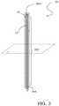
- FIG. 3schematically shows a contact probe according to an embodiment of the disclosure.
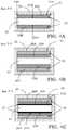
- FIGS. 4A-4Eschematically show an enlarged cross section of a contact probe according to different embodiments of the disclosure.
- a contact probe for a testing head of an apparatus for testing electronic devices integrated on a waferis described and globally indicated with 30 .
- the contact probe 30includes at least one contact tip 30 A apt to abut on a contact pad of a device under test, not shown as it is conventional.
- the contact probe 30can also include, as shown in the example of FIG. 3 , a contact head 30 B, having same or different shape with respect to the contact tip 30 A. That contact head 30 B can be intended to abut on a contact pad of a space transformer, as in the case of non-blocked probes, or can be fixedly associated, for example soldered, to a ceramic support, as in the case of the probes protruding from that support.
- the contact probe 30also comprises a body 30 C essentially extended according to a longitudinal direction between the contact tip 30 A and the contact head 30 B.
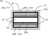
- the contact probe 30comprises a multilayer structure 31 , in turn including at least one inner layer 32 or core made of a first material, in particular nickel-tungsten NiW, coated at two opposite sides thereof by a first inner coating layer 33 , in particular a high conductivity layer, for example made of gold Au, as schematically shown in FIGS. 4A-4E , which represent sections P-P being taken at a plane n shown in FIG. 3 .
- the first inner coating layer 33includes a first portion 33 A arranged at a first side 32 A of the core 32 , for example an upper side in the local reference system of FIGS. 4A-4E , as well as a second portion 33 B at a second side 32 B of the core 32 , for example a lower side.
- the multilayer structure 31has at least one first edge portion 34 A and a second edge portion 34 B where the core 32 and also the first inner coating layer 33 are exposed. It is clear to one skilled in the art that those edge portions 34 A, 34 B can result, for example, from a laser cut of the contact probe 30 starting from a multilayer sheet.
- the contact probe 30also includes an outer coating layer 35 , in particular a high hardness layer, for example made of rhodium Rd, which completely covers the contact probe 30 itself and thus covers the exposed portions of the core 32 and of the first inner coating layer 33 .
- an outer coating layer 35in particular a high hardness layer, for example made of rhodium Rd, which completely covers the contact probe 30 itself and thus covers the exposed portions of the core 32 and of the first inner coating layer 33 .
- the multilayer structure 31 of the contact probe 30can include a second inner coating layer 36 that covers the first inner coating layer 33 .
- the first portion 33 A of the first inner coating layer 33is covered by a first portion 36 A of the second inner coating layer 36 always arranged at the first side 32 A of the core 32 .
- the first portion 33 A of the first inner coating layer 33is contacting the core 32 , right at the first side 32 A, and the first portion 36 A of the second inner coating layer 36 is contacting the first portion 33 A of the first inner coating layer 33 .
- the second portion 33 B of the first inner coating layer 33is covered by a second portion 36 B of the second inner coating layer 36 always arranged at the second side 32 B of the core 32 .
- the multilayer structure 31also includes an adhesive film 37 , disposed between the core 32 and the first inner coating layer 33 and made of a material apt to facilitate the adhesion of the first inner coating layer 33 on the core 32 .
- the adhesive film 37includes a first portion 37 A arranged between the core 32 and the first portion 33 A of the first inner coating layer 33 and a second portion 37 B arranged between the core 32 and the second portion 33 B of the first inner coating layer 33 .
- the multilayer structure 31can include a plurality of first inner coating layers 33 i and second inner coating layers 36 i arranged in an alternated manner and in any number at the first and second side 32 A, 32 B of the core 32 .
- the multilayer structure 31can include one or more adhesive films 37 i arranged between the core 32 and a first inner coating layer 33 , as well as between a second inner coating layer 36 and a further first inner coating layer 33 .
- the contact probe 30also includes a protective layer 38 , which completely surrounds the multilayer structure 31 , and is interposed between the multilayer structure 31 and the outer coating layer 35 .
- Typical dimensional ranges for the different elements of the contact probe 30 according to the disclosureare the following:
- Typical length values of a contact proberange from 2 to 9 mm.
- the contact probe 30has a substantially rectangular section. Obviously, the same could have a section having any prismatic shape.
- the core 32is made of a first conductive material, in particular a metal or a metal alloy, such as nickel or an alloy thereof, such as the nickel-manganese NiMn, nickel-cobalt NiCo or nickel-tungsten NiW alloys.
- the core 32is made of nickel-tungsten NiW.
- the core 32can also be made of a non-conductive material, for example silicon Si.
- the first inner coating layer 33is made of a second conductive material, in particular a metal material having high electrical and thermal conductivity values, in particular greater than the values of the first conductive material. Therefore, that metal material is selected among copper Cu, silver Ag, gold Au or alloys thereof. In a preferred embodiment of the disclosure, the first inner coating layer 33 is made of copper Cu.
- the second inner coating layer 36can be made of the same second conductive material, the alternation between the first inner coating layer 33 and the second inner coating layer 36 allowing making a more homogeneous multilayer structure 31 thanks to the use of individually thinner layers.
- the presence of the first inner coating layer 33 having high conductivity, i.e. low resistivity,modifies the electrical behavior of the contact probe 30 .
- the presence of that high conductivity layeressentially realizes a resistance in parallel to the resistance of the core 32 of the multilayer structure 31 of the contact probe 30 .
- the currentflows along the whole section of the contact probe 30 , namely in the core 32 , for example made of nickel-tungsten, and in the first inner coating layer 33 having high conductivity, for example made of copper.
- the contact probe 30is made of a material having a conductivity being the average value between the conductivity of the first inner coating layer 33 having high conductivity and the one of the core 32 , for example between copper and nickel-tungsten.
- a current applied to the contact probe 30in any case, will prefer the less resistance path and will flow mainly in the first inner coating layer 33 having high conductivity.
- the behavior of the contact probe 30is further improved under alternating current conditions.
- skin effectthe current flowing across the multilayer structure 31 of the contact probe 30 tends to flow substantially only in its external part, namely at the first inner coating layer 33 that is the one having the highest conductivity.
- skin effectindicates the phenomenon in which an alternating electrical current tends to be distributed inside a conductor in a non-uniform manner: the current density is higher on the conductor surface and lower inside the same.
- the current densityi.e. the current per unit area of a conductor
- the current densitydecreases exponentially penetrating progressively from the outer surface towards its inner part. This is true for circular section or other shape conductors, as in the case of the contact probes of a testing head.
- the contact probe 30is able to sustain higher current densities than a traditional probe entirely made of nickel-tungsten, since most of the current applied thereto flows into its first inner coating layer 33 having high conductivity, i.e. lower resistivity.
- the contact probe 30is able to sustain yet higher current densities in case of alternating currents which, due to the skin effect, tend to flow only in that first inner coating layer 33 having high conductivity.
- Such a contact probe 30also has lower leakages during the test signals transmission. Finally, the presence of the first inner coating layer 33 having high conductivity guarantees a better heat dissipation by the multilayer structure 31 of the contact probe 30 .
- the outer coating layer 35is made of a third conductive material having higher hardness with respect to the one of the first conductive material making the core 32 of the multilayer structure 31 .
- the third conductive materialis a metal or a metal alloy, in particular rhodium Rd, platinum Pt, iridium Ir or a metal alloy thereof or a palladium-cobalt PdCo alloy, a palladium-nickel PdNi alloy or a nickel-phosphor NiPh alloy.
- the outer coating layer 35is made of rhodium Rd.
- the third conductive materialis selected in order to have a good electrical conductivity and thus in order not to significantly worsen the values measured by the contact probe.
- the presence of the outer coating layer 35allows providing the contact probe 30 with a higher external hardness and improving its sliding through the guide holes realized in the plate-shaped guides of the testing head including it, protecting the exposed portions of the layers of the multilayer structure 31 . In that way, when the probe is slidingly assembled in guide holes realized in plate-shaped guides, in particular ceramic ones, abrasions or “peelings” of the probe itself do not occur during the operation.
- the outer coating layer 35 made of rhodiumgenerally improves the mechanical performance of the probe.
- the outer coating layer 35 made of rhodium, which completely covers the contact probe 30 , including its contact tip 30 A,allows incrementing the probe working life, guaranteeing its proper operation for a high number of testing operations where that tip 30 A is in pressing contact on the contact pads of a device under test and also during many tip cleaning and re-shape operations which usually involve abrasive cloths.
- the presence of the outer coating layer 35prevents the damage and the oxidation of the core 32 and of the first inner coating layer 33 , in particular at the exposed edge portions 34 A and 34 B, which edge portions are covered by the outer coating layer 35 .
- the adhesive film 37can be made of a metal or a metal alloy, in particular gold Au, silver Ag, platinum Pt or a metal alloy thereof, preferably gold Au, in order to improve the adhesion of the first inner coating layer 33 , having high conductivity, on the core 32 .
- filmit is meant, as it is known in this technical field, a layer having a thickness between 0.01 and 0.5 ⁇ m.
- the protective layer 38is made of a metal or a metal alloy, in particular rhodium Rd, gold Au, platinum Pt, palladium Pd or a metallic alloy thereof or a palladium-cobalt PdCo alloy, preferably palladium Pd, and it is adapted to protect the multilayer structure 31 from corrosive agents able to penetrate in the outer coating layer 35 .
- rhodiumto make the outer coating layer 35 , the same is quite porous and allows the oxygen passage which could oxidize the first inner coating layer 33 having high conductivity, for example made of copper, of the multilayer structure 31 . That oxidation can be prevented by using a protective layer 38 , for example made of palladium, interposed between the multilayer structure 31 , and thus the first inner coating layer 33 , and the outer coating layer 35 .
- a protective layer 38 made of palladiumis not permeable to the oxygen, which oxygen thus cannot reach the first inner coating layer 33 having high conductivity and thus cannot damage it.
- a testing headcomprises a plurality of probes made according to the contact probe 30 of the present disclosure.
- a testing headcould include an upper guide and a lower guide in a spaced apart relation from each other in order to define an air gap and provided with respective upper and lower guide holes inside which that plurality of contact probes slide.
- the testing headcould include a plate-shaped support, in particular a ceramic one, to which the plurality of contact probes is fixedly fastened at the probe heads, while the probe tips freely protrude starting from the plate-shaped support in order to abut on a corresponding plurality of contact pads of a device under test.
- the contact probe according to the disclosurecan be made staring from a multilayer sheet, by means of laser cutting thereof.
- a photolithographic technologynamely by means of a so-called MEMS Process.
- the improved contact probe performancessuch as the improved current capability due to the high conductivity layer and the hardness of the outer coating layer, it is possible to reduce the cross-section and consequently also the length of the probe, for example up to halving it compared to known probes used for similar applications. It is immediately clear that the probe length reduction, the performances being equal, allows reducing the RLC parasitic effects and in particular the inductance value, with an advantage on the performances of the overall contact probe, in particular the frequency performances.
Landscapes
- Physics & Mathematics (AREA)
- General Physics & Mathematics (AREA)
- Engineering & Computer Science (AREA)
- Computer Hardware Design (AREA)
- Microelectronics & Electronic Packaging (AREA)
- General Engineering & Computer Science (AREA)
- Geometry (AREA)
- Measuring Leads Or Probes (AREA)
- Testing Or Measuring Of Semiconductors Or The Like (AREA)
Abstract
Description
- a core32 having section from 10×10 to 50×50 μm;
- a high conductivity first
inner coating layer 33 having thickness from 0.5 to 20 μm; - a second
inner coating layer 36 having thickness from 0.5 to 20 μm; and - an
outer coating layer 35 having thickness from 0.01 to 5 μm.
Claims (29)
Applications Claiming Priority (3)
| Application Number | Priority Date | Filing Date | Title |
|---|---|---|---|
| ITMI20142286 | 2014-12-30 | ||
| ITMI2014A002286 | 2014-12-30 | ||
| PCT/EP2015/079544WO2016107729A1 (en) | 2014-12-30 | 2015-12-14 | Contact probe for testing head |
Related Parent Applications (1)
| Application Number | Title | Priority Date | Filing Date |
|---|---|---|---|
| PCT/EP2015/079544Continuation-In-PartWO2016107729A1 (en) | 2014-12-30 | 2015-12-14 | Contact probe for testing head |
Publications (2)
| Publication Number | Publication Date |
|---|---|
| US20170307657A1 US20170307657A1 (en) | 2017-10-26 |
| US11131690B2true US11131690B2 (en) | 2021-09-28 |
Family
ID=52633392
Family Applications (1)
| Application Number | Title | Priority Date | Filing Date |
|---|---|---|---|
| US15/640,097ActiveUS11131690B2 (en) | 2014-12-30 | 2017-06-30 | Contact probe for testing head |
Country Status (9)
| Country | Link |
|---|---|
| US (1) | US11131690B2 (en) |
| EP (1) | EP3241028B1 (en) |
| JP (1) | JP6759213B2 (en) |
| KR (2) | KR102542154B1 (en) |
| CN (1) | CN107257928B (en) |
| PH (1) | PH12017501220B1 (en) |
| SG (1) | SG11201704433TA (en) |
| TW (1) | TWI679425B (en) |
| WO (1) | WO2016107729A1 (en) |
Cited By (12)
| Publication number | Priority date | Publication date | Assignee | Title |
|---|---|---|---|---|
| US11268204B2 (en)* | 2020-03-24 | 2022-03-08 | Dongguan Leader Precision Industry Co., Ltd. | Metallic terminal and manufacturing method thereof |
| US11761982B1 (en) | 2019-12-31 | 2023-09-19 | Microfabrica Inc. | Probes with planar unbiased spring elements for electronic component contact and methods for making such probes |
| US11774467B1 (en) | 2020-09-01 | 2023-10-03 | Microfabrica Inc. | Method of in situ modulation of structural material properties and/or template shape |
| US11802891B1 (en) | 2019-12-31 | 2023-10-31 | Microfabrica Inc. | Compliant pin probes with multiple spring segments and compression spring deflection stabilization structures, methods for making, and methods for using |
| US11973301B2 (en) | 2018-09-26 | 2024-04-30 | Microfabrica Inc. | Probes having improved mechanical and/or electrical properties for making contact between electronic circuit elements and methods for making |
| US12000865B2 (en) | 2019-02-14 | 2024-06-04 | Microfabrica Inc. | Multi-beam vertical probes with independent arms formed of a high conductivity metal for enhancing current carrying capacity and methods for making such probes |
| US12078657B2 (en) | 2019-12-31 | 2024-09-03 | Microfabrica Inc. | Compliant pin probes with extension springs, methods for making, and methods for using |
| US12146898B2 (en) | 2020-10-02 | 2024-11-19 | Microfabrica Inc. | Multi-beam probes with decoupled structural and current carrying beams and methods of making |
| US12181493B2 (en) | 2018-10-26 | 2024-12-31 | Microfabrica Inc. | Compliant probes including dual independently operable probe contact elements including at least one flat extension spring, methods for making, and methods for using |
| US12196782B2 (en) | 2019-12-31 | 2025-01-14 | Microfabrica Inc. | Probes with planar unbiased spring elements for electronic component contact, methods for making such probes, and methods for using such probes |
| US12196781B2 (en) | 2019-12-31 | 2025-01-14 | Microfabrica Inc. | Probes with planar unbiased spring elements for electronic component contact, methods for making such probes, and methods for using such probes |
| US12210038B2 (en) | 2022-05-11 | 2025-01-28 | Tse Co., Ltd. | Method of manufacturing a probe tip and a probe tip manufactured by the same |
Families Citing this family (28)
| Publication number | Priority date | Publication date | Assignee | Title |
|---|---|---|---|---|
| JP6221031B1 (en) | 2016-12-16 | 2017-11-01 | 日本電産リード株式会社 | Contact probe and electrical connection jig |
| IT201700021397A1 (en) | 2017-02-24 | 2018-08-24 | Technoprobe Spa | Measuring head with improved frequency properties |
| JP7005939B2 (en)* | 2017-05-25 | 2022-01-24 | 日本電産リード株式会社 | Contact probe |
| CN109425814B (en)* | 2017-09-01 | 2021-09-10 | 中华精测科技股份有限公司 | Probe assembly and probe structure thereof |
| CN109425762B (en)* | 2017-09-01 | 2021-05-07 | 中华精测科技股份有限公司 | Probe assembly and probe structure thereof |
| US20190103693A1 (en)* | 2017-09-29 | 2019-04-04 | Apple Inc. | Electrical contacts having sacrificial layer for corrosion protection |
| US11262383B1 (en)* | 2018-09-26 | 2022-03-01 | Microfabrica Inc. | Probes having improved mechanical and/or electrical properties for making contact between electronic circuit elements and methods for making |
| CN113287024A (en)* | 2019-01-29 | 2021-08-20 | 株式会社友华 | Plunger and contact probe |
| TWI714151B (en)* | 2019-07-01 | 2020-12-21 | 技鼎股份有限公司 | Probe head and conductive probe thereof |
| TWI822833B (en)* | 2019-08-15 | 2023-11-21 | 優顯科技股份有限公司 | Electronic detection interface, electronic detection module using the same, and electronic detection method applicable of the same |
| IT201900024889A1 (en)* | 2019-12-19 | 2021-06-19 | Technoprobe Spa | Contact probe for high frequency applications with improved current carrying capacity |
| CN113109603A (en)* | 2020-01-13 | 2021-07-13 | 科磊股份有限公司 | Cantilever probe with multiple metal coatings |
| EP3862759B1 (en)* | 2020-02-04 | 2022-05-11 | Heraeus Deutschland GmbH & Co. KG | Sheathed wire and method for producing same |
| JP7605203B2 (en)* | 2020-03-19 | 2024-12-24 | ニデックアドバンステクノロジー株式会社 | Contact terminal, inspection tool, and inspection device |
| JPWO2022059070A1 (en)* | 2020-09-15 | 2022-03-24 | ||
| KR102517778B1 (en)* | 2021-02-26 | 2023-04-04 | (주)포인트엔지니어링 | The Electro-conductive Contact Pin Assembly and Method for Manufacturing Thereof |
| US20230258689A1 (en) | 2021-03-16 | 2023-08-17 | Japan Electronic Materials Corporation | Probe of probe card use, and method for manufacturing the same |
| KR102549551B1 (en)* | 2021-04-06 | 2023-06-29 | (주)포인트엔지니어링 | The electro-conductive contact pin and inspection apparatus having the same electro-conductive pin and manufacturing method thereof |
| KR102577539B1 (en)* | 2021-04-09 | 2023-09-12 | (주)포인트엔지니어링 | The Electro-conductive Contact Pin and Manufacturing Method thereof |
| KR102321083B1 (en)* | 2021-07-21 | 2021-11-03 | (주)새한마이크로텍 | Contact Probe |
| CN113507005A (en)* | 2021-08-10 | 2021-10-15 | 烟台艾睿光电科技有限公司 | Patrol and examine robot room of charging and patrol and examine robot |
| CN114791517B (en)* | 2022-04-18 | 2025-06-03 | 苏州伊欧陆系统集成有限公司 | A low leakage and high temperature resistant ceramic blade test probe |
| TW202424495A (en)* | 2022-08-15 | 2024-06-16 | 美商微製造股份有限公司 | Multi-beam probes with decoupled structural and current carrying beams |
| EP4325227B1 (en)* | 2022-08-16 | 2025-10-01 | Heraeus Precious Metals GmbH & Co. KG | Tape-like composite material for test needles |
| JP2024070404A (en)* | 2022-11-11 | 2024-05-23 | 株式会社日本マイクロニクス | Probes and Electrical Connection Devices |
| JP2024081055A (en)* | 2022-12-05 | 2024-06-17 | 株式会社日本マイクロニクス | Probes and Electrical Connection Devices |
| JP2024082419A (en)* | 2022-12-08 | 2024-06-20 | 株式会社日本マイクロニクス | probe |
| JP2025117043A (en)* | 2024-01-30 | 2025-08-12 | 株式会社日本マイクロニクス | Probes and Electrical Connection Devices |
Citations (13)
| Publication number | Priority date | Publication date | Assignee | Title |
|---|---|---|---|---|
| WO2000079293A1 (en) | 1999-06-22 | 2000-12-28 | International Test Solutions, Inc. | Probe device using superelastic probe elements |
| US20020089344A1 (en)* | 1996-09-13 | 2002-07-11 | Beaman Brian Samuel | Probe structure having a plurality of discrete insulated probe tips projecting from a support surface, apparatus for use thereof and methods of fabrication thereof |
| US20020127812A1 (en)* | 1999-12-21 | 2002-09-12 | Kabushiki Kaisha Toshiba | Probe pin for testing electrical characteristics of apparatus, probe card using probe pins |
| US6573738B1 (en)* | 1999-03-25 | 2003-06-03 | Tokyo Cathode Laboratory Co., Ltd. | Multi-layered probe for a probecard |
| US20040239355A1 (en)* | 2001-07-02 | 2004-12-02 | Toshio Kazama | Conductive contact |
| US20050227510A1 (en)* | 2004-04-09 | 2005-10-13 | Brown Dirk D | Small array contact with precision working range |
| US20070200576A1 (en)* | 2006-02-08 | 2007-08-30 | Laurent Edward T | Multi-layered probes |
| US20080074128A1 (en)* | 2006-09-26 | 2008-03-27 | Kabushiki Kaisha Nihon Micronics | Electrical test probe and electrical test probe assembly |
| US20080143366A1 (en) | 2004-12-14 | 2008-06-19 | Fumio Kurotori | Contact Pin Probe Card and Electronic Device Test Apparatus Using Same |
| EP2060921A1 (en) | 2007-11-16 | 2009-05-20 | Technoprobe S.p.A | Contact probe for testing head having vertical probes and related testing head for testing microstructure electric performance |
| US20090243637A1 (en)* | 2008-03-31 | 2009-10-01 | Hitachi High-Technologies Corporation | Measuring apparatus having nanotube probe |
| US20130099813A1 (en) | 2011-10-21 | 2013-04-25 | Tokyo Electron Limited | Contact terminal for a probe card, and the probe card |
| US20150280345A1 (en)* | 2012-12-04 | 2015-10-01 | Japan Electronic Materials Corporation | Electrical Contact |
Family Cites Families (15)
| Publication number | Priority date | Publication date | Assignee | Title |
|---|---|---|---|---|
| JPH04351968A (en)* | 1991-05-29 | 1992-12-07 | Vacuum Metallurgical Co Ltd | Probe |
| JP3215452B2 (en)* | 1991-05-30 | 2001-10-09 | 真空冶金株式会社 | Electrode |
| KR100324059B1 (en)* | 1994-11-15 | 2002-04-17 | 이고르 와이. 칸드로스 | Interconnection Elements for Microelectronic Components |
| KR100266389B1 (en)* | 1995-05-26 | 2000-09-15 | 이고르 와이. 칸드로스 | Contact carriers (tiles) for anchoring large substrates with spring contacts |
| JP3458684B2 (en)* | 1997-11-28 | 2003-10-20 | 三菱マテリアル株式会社 | Contact probe |
| EP1135690B1 (en) | 1998-12-02 | 2003-06-04 | Formfactor, Inc. | Lithographic contact elements |
| JP2002131334A (en)* | 2000-10-24 | 2002-05-09 | Nec Yamaguchi Ltd | Probe needle, probe card, and manufacturing method of probe card |
| JP2003057266A (en)* | 2001-08-20 | 2003-02-26 | Mitsubishi Materials Corp | Contact probe and manufacturing method therefor |
| DE60227277D1 (en)* | 2001-09-24 | 2008-08-07 | Rika Denshi America Inc | ELECTRICAL TESTS AND METHOD FOR THE PRODUCTION THEREOF |
| JP3837434B2 (en)* | 2003-06-20 | 2006-10-25 | アルプス電気株式会社 | Connected device |
| JP2007327854A (en)* | 2006-06-08 | 2007-12-20 | Nidec-Read Corp | Board inspection tool and board inspection apparatus |
| US7836587B2 (en)* | 2006-09-21 | 2010-11-23 | Formfactor, Inc. | Method of repairing a contactor apparatus |
| JP4783265B2 (en)* | 2006-11-02 | 2011-09-28 | 健 金子 | Contact probe and method of manufacturing contact probe |
| US20120176122A1 (en)* | 2010-03-30 | 2012-07-12 | Yoshihiro Hirata | Contact probe, linked body of contact probes, and manufacturing methods thereof |
| KR101064852B1 (en) | 2010-05-24 | 2011-09-14 | 김재길 | Needle for probe card |
- 2015
- 2015-12-14EPEP15823139.9Apatent/EP3241028B1/enactiveActive
- 2015-12-14WOPCT/EP2015/079544patent/WO2016107729A1/enactiveApplication Filing
- 2015-12-14JPJP2017535369Apatent/JP6759213B2/enactiveActive
- 2015-12-14KRKR1020227037896Apatent/KR102542154B1/enactiveActive
- 2015-12-14CNCN201580070711.9Apatent/CN107257928B/enactiveActive
- 2015-12-14KRKR1020177021268Apatent/KR102502965B1/enactiveActive
- 2015-12-14SGSG11201704433TApatent/SG11201704433TA/enunknown
- 2015-12-29TWTW104144231Apatent/TWI679425B/enactive
- 2017
- 2017-06-29PHPH12017501220Apatent/PH12017501220B1/enunknown
- 2017-06-30USUS15/640,097patent/US11131690B2/enactiveActive
Patent Citations (13)
| Publication number | Priority date | Publication date | Assignee | Title |
|---|---|---|---|---|
| US20020089344A1 (en)* | 1996-09-13 | 2002-07-11 | Beaman Brian Samuel | Probe structure having a plurality of discrete insulated probe tips projecting from a support surface, apparatus for use thereof and methods of fabrication thereof |
| US6573738B1 (en)* | 1999-03-25 | 2003-06-03 | Tokyo Cathode Laboratory Co., Ltd. | Multi-layered probe for a probecard |
| WO2000079293A1 (en) | 1999-06-22 | 2000-12-28 | International Test Solutions, Inc. | Probe device using superelastic probe elements |
| US20020127812A1 (en)* | 1999-12-21 | 2002-09-12 | Kabushiki Kaisha Toshiba | Probe pin for testing electrical characteristics of apparatus, probe card using probe pins |
| US20040239355A1 (en)* | 2001-07-02 | 2004-12-02 | Toshio Kazama | Conductive contact |
| US20050227510A1 (en)* | 2004-04-09 | 2005-10-13 | Brown Dirk D | Small array contact with precision working range |
| US20080143366A1 (en) | 2004-12-14 | 2008-06-19 | Fumio Kurotori | Contact Pin Probe Card and Electronic Device Test Apparatus Using Same |
| US20070200576A1 (en)* | 2006-02-08 | 2007-08-30 | Laurent Edward T | Multi-layered probes |
| US20080074128A1 (en)* | 2006-09-26 | 2008-03-27 | Kabushiki Kaisha Nihon Micronics | Electrical test probe and electrical test probe assembly |
| EP2060921A1 (en) | 2007-11-16 | 2009-05-20 | Technoprobe S.p.A | Contact probe for testing head having vertical probes and related testing head for testing microstructure electric performance |
| US20090243637A1 (en)* | 2008-03-31 | 2009-10-01 | Hitachi High-Technologies Corporation | Measuring apparatus having nanotube probe |
| US20130099813A1 (en) | 2011-10-21 | 2013-04-25 | Tokyo Electron Limited | Contact terminal for a probe card, and the probe card |
| US20150280345A1 (en)* | 2012-12-04 | 2015-10-01 | Japan Electronic Materials Corporation | Electrical Contact |
Cited By (15)
| Publication number | Priority date | Publication date | Assignee | Title |
|---|---|---|---|---|
| US11973301B2 (en) | 2018-09-26 | 2024-04-30 | Microfabrica Inc. | Probes having improved mechanical and/or electrical properties for making contact between electronic circuit elements and methods for making |
| US12181493B2 (en) | 2018-10-26 | 2024-12-31 | Microfabrica Inc. | Compliant probes including dual independently operable probe contact elements including at least one flat extension spring, methods for making, and methods for using |
| US12000865B2 (en) | 2019-02-14 | 2024-06-04 | Microfabrica Inc. | Multi-beam vertical probes with independent arms formed of a high conductivity metal for enhancing current carrying capacity and methods for making such probes |
| US11802891B1 (en) | 2019-12-31 | 2023-10-31 | Microfabrica Inc. | Compliant pin probes with multiple spring segments and compression spring deflection stabilization structures, methods for making, and methods for using |
| US11867721B1 (en) | 2019-12-31 | 2024-01-09 | Microfabrica Inc. | Probes with multiple springs, methods for making, and methods for using |
| US11906549B1 (en) | 2019-12-31 | 2024-02-20 | Microfabrica Inc. | Compliant pin probes with flat extension springs, methods for making, and methods for using |
| US12066462B2 (en) | 2019-12-31 | 2024-08-20 | Microfabrica Inc. | Probes with planar unbiased spring elements for electronic component contact and methods for making such probes |
| US12078657B2 (en) | 2019-12-31 | 2024-09-03 | Microfabrica Inc. | Compliant pin probes with extension springs, methods for making, and methods for using |
| US11761982B1 (en) | 2019-12-31 | 2023-09-19 | Microfabrica Inc. | Probes with planar unbiased spring elements for electronic component contact and methods for making such probes |
| US12196782B2 (en) | 2019-12-31 | 2025-01-14 | Microfabrica Inc. | Probes with planar unbiased spring elements for electronic component contact, methods for making such probes, and methods for using such probes |
| US12196781B2 (en) | 2019-12-31 | 2025-01-14 | Microfabrica Inc. | Probes with planar unbiased spring elements for electronic component contact, methods for making such probes, and methods for using such probes |
| US11268204B2 (en)* | 2020-03-24 | 2022-03-08 | Dongguan Leader Precision Industry Co., Ltd. | Metallic terminal and manufacturing method thereof |
| US11774467B1 (en) | 2020-09-01 | 2023-10-03 | Microfabrica Inc. | Method of in situ modulation of structural material properties and/or template shape |
| US12146898B2 (en) | 2020-10-02 | 2024-11-19 | Microfabrica Inc. | Multi-beam probes with decoupled structural and current carrying beams and methods of making |
| US12210038B2 (en) | 2022-05-11 | 2025-01-28 | Tse Co., Ltd. | Method of manufacturing a probe tip and a probe tip manufactured by the same |
Also Published As
| Publication number | Publication date |
|---|---|
| CN107257928A (en) | 2017-10-17 |
| JP6759213B2 (en) | 2020-09-23 |
| KR20170107465A (en) | 2017-09-25 |
| PH12017501220B1 (en) | 2020-11-18 |
| KR102502965B1 (en) | 2023-02-23 |
| EP3241028B1 (en) | 2020-02-05 |
| TWI679425B (en) | 2019-12-11 |
| WO2016107729A1 (en) | 2016-07-07 |
| CN107257928B (en) | 2020-12-01 |
| US20170307657A1 (en) | 2017-10-26 |
| KR20220153661A (en) | 2022-11-18 |
| TW201629493A (en) | 2016-08-16 |
| PH12017501220A1 (en) | 2018-01-08 |
| KR102542154B1 (en) | 2023-06-13 |
| EP3241028A1 (en) | 2017-11-08 |
| JP2018501490A (en) | 2018-01-18 |
| SG11201704433TA (en) | 2017-07-28 |
Similar Documents
| Publication | Publication Date | Title |
|---|---|---|
| US11131690B2 (en) | Contact probe for testing head | |
| US20170122980A1 (en) | Contact probe for a testing head and corresponding manufacturing method | |
| US10228392B2 (en) | Contact probe for a testing head | |
| KR102156364B1 (en) | Electrical connection device | |
| KR102015798B1 (en) | Probe for the test device | |
| JP6872960B2 (en) | Electrical connection device | |
| TWI623751B (en) | Probe device and rectangular probe | |
| US20190086443A1 (en) | Probe card device and round probe thereof | |
| JP7496716B2 (en) | Probe unit and method for producing same | |
| JP4624372B2 (en) | Multilayer electrical probe | |
| KR20230049214A (en) | The Electro-conductive Contact Pin and Testing Device Having The Same | |
| JP2007132681A (en) | Probe and manufacturing method thereof | |
| KR20230082598A (en) | contact probe | |
| WO2024232152A1 (en) | Probe and electrical connection device | |
| ITMI20110896A1 (en) | CONTACTING PROBE FOR MEASURING HEAD |
Legal Events
| Date | Code | Title | Description |
|---|---|---|---|
| AS | Assignment | Owner name:TECHNOPROBE S.P.A., ITALY Free format text:ASSIGNMENT OF ASSIGNORS INTEREST;ASSIGNOR:CRIPPA, GIUSEPPE;REEL/FRAME:042911/0368 Effective date:20170626 | |
| FEPP | Fee payment procedure | Free format text:ENTITY STATUS SET TO SMALL (ORIGINAL EVENT CODE: SMAL); ENTITY STATUS OF PATENT OWNER: LARGE ENTITY Free format text:ENTITY STATUS SET TO UNDISCOUNTED (ORIGINAL EVENT CODE: BIG.); ENTITY STATUS OF PATENT OWNER: LARGE ENTITY | |
| STPP | Information on status: patent application and granting procedure in general | Free format text:RESPONSE TO NON-FINAL OFFICE ACTION ENTERED AND FORWARDED TO EXAMINER | |
| STPP | Information on status: patent application and granting procedure in general | Free format text:FINAL REJECTION MAILED | |
| STPP | Information on status: patent application and granting procedure in general | Free format text:DOCKETED NEW CASE - READY FOR EXAMINATION | |
| STPP | Information on status: patent application and granting procedure in general | Free format text:NON FINAL ACTION MAILED | |
| STPP | Information on status: patent application and granting procedure in general | Free format text:RESPONSE TO NON-FINAL OFFICE ACTION ENTERED AND FORWARDED TO EXAMINER | |
| STPP | Information on status: patent application and granting procedure in general | Free format text:NOTICE OF ALLOWANCE MAILED -- APPLICATION RECEIVED IN OFFICE OF PUBLICATIONS | |
| STPP | Information on status: patent application and granting procedure in general | Free format text:PUBLICATIONS -- ISSUE FEE PAYMENT VERIFIED | |
| STCF | Information on status: patent grant | Free format text:PATENTED CASE | |
| CC | Certificate of correction | ||
| MAFP | Maintenance fee payment | Free format text:PAYMENT OF MAINTENANCE FEE, 4TH YEAR, LARGE ENTITY (ORIGINAL EVENT CODE: M1551); ENTITY STATUS OF PATENT OWNER: LARGE ENTITY Year of fee payment:4 |