US11126902B2 - Optically variable data storage device - Google Patents
Optically variable data storage deviceDownload PDFInfo
- Publication number
- US11126902B2 US11126902B2US16/133,210US201816133210AUS11126902B2US 11126902 B2US11126902 B2US 11126902B2US 201816133210 AUS201816133210 AUS 201816133210AUS 11126902 B2US11126902 B2US 11126902B2
- Authority
- US
- United States
- Prior art keywords
- data
- optical
- storage layer
- angle
- data storage
- Prior art date
- Legal status (The legal status is an assumption and is not a legal conclusion. Google has not performed a legal analysis and makes no representation as to the accuracy of the status listed.)
- Active, expires
Links
Images


Classifications
- G—PHYSICS
- G06—COMPUTING OR CALCULATING; COUNTING
- G06K—GRAPHICAL DATA READING; PRESENTATION OF DATA; RECORD CARRIERS; HANDLING RECORD CARRIERS
- G06K19/00—Record carriers for use with machines and with at least a part designed to carry digital markings
- G06K19/06—Record carriers for use with machines and with at least a part designed to carry digital markings characterised by the kind of the digital marking, e.g. shape, nature, code
- G06K19/06009—Record carriers for use with machines and with at least a part designed to carry digital markings characterised by the kind of the digital marking, e.g. shape, nature, code with optically detectable marking
- G06K19/06037—Record carriers for use with machines and with at least a part designed to carry digital markings characterised by the kind of the digital marking, e.g. shape, nature, code with optically detectable marking multi-dimensional coding
- G—PHYSICS
- G06—COMPUTING OR CALCULATING; COUNTING
- G06K—GRAPHICAL DATA READING; PRESENTATION OF DATA; RECORD CARRIERS; HANDLING RECORD CARRIERS
- G06K19/00—Record carriers for use with machines and with at least a part designed to carry digital markings
- G06K19/06—Record carriers for use with machines and with at least a part designed to carry digital markings characterised by the kind of the digital marking, e.g. shape, nature, code
- G06K19/06009—Record carriers for use with machines and with at least a part designed to carry digital markings characterised by the kind of the digital marking, e.g. shape, nature, code with optically detectable marking
- G06K19/06046—Constructional details
- G06K19/06084—Constructional details the marking being based on nanoparticles or microbeads
- G—PHYSICS
- G06—COMPUTING OR CALCULATING; COUNTING
- G06K—GRAPHICAL DATA READING; PRESENTATION OF DATA; RECORD CARRIERS; HANDLING RECORD CARRIERS
- G06K19/00—Record carriers for use with machines and with at least a part designed to carry digital markings
- G06K19/06—Record carriers for use with machines and with at least a part designed to carry digital markings characterised by the kind of the digital marking, e.g. shape, nature, code
- G06K19/06009—Record carriers for use with machines and with at least a part designed to carry digital markings characterised by the kind of the digital marking, e.g. shape, nature, code with optically detectable marking
- G06K19/06046—Constructional details
- G06K19/0614—Constructional details the marking being selective to wavelength, e.g. color barcode or barcodes only visible under UV or IR
- G—PHYSICS
- G06—COMPUTING OR CALCULATING; COUNTING
- G06K—GRAPHICAL DATA READING; PRESENTATION OF DATA; RECORD CARRIERS; HANDLING RECORD CARRIERS
- G06K7/00—Methods or arrangements for sensing record carriers, e.g. for reading patterns
- G06K7/10—Methods or arrangements for sensing record carriers, e.g. for reading patterns by electromagnetic radiation, e.g. optical sensing; by corpuscular radiation
- G06K7/10544—Methods or arrangements for sensing record carriers, e.g. for reading patterns by electromagnetic radiation, e.g. optical sensing; by corpuscular radiation by scanning of the records by radiation in the optical part of the electromagnetic spectrum
- G06K7/10712—Fixed beam scanning
- G06K7/10722—Photodetector array or CCD scanning
- G—PHYSICS
- G06—COMPUTING OR CALCULATING; COUNTING
- G06K—GRAPHICAL DATA READING; PRESENTATION OF DATA; RECORD CARRIERS; HANDLING RECORD CARRIERS
- G06K7/00—Methods or arrangements for sensing record carriers, e.g. for reading patterns
- G06K7/10—Methods or arrangements for sensing record carriers, e.g. for reading patterns by electromagnetic radiation, e.g. optical sensing; by corpuscular radiation
- G06K7/10544—Methods or arrangements for sensing record carriers, e.g. for reading patterns by electromagnetic radiation, e.g. optical sensing; by corpuscular radiation by scanning of the records by radiation in the optical part of the electromagnetic spectrum
- G06K7/10821—Methods or arrangements for sensing record carriers, e.g. for reading patterns by electromagnetic radiation, e.g. optical sensing; by corpuscular radiation by scanning of the records by radiation in the optical part of the electromagnetic spectrum further details of bar or optical code scanning devices
- B—PERFORMING OPERATIONS; TRANSPORTING
- B82—NANOTECHNOLOGY
- B82Y—SPECIFIC USES OR APPLICATIONS OF NANOSTRUCTURES; MEASUREMENT OR ANALYSIS OF NANOSTRUCTURES; MANUFACTURE OR TREATMENT OF NANOSTRUCTURES
- B82Y20/00—Nanooptics, e.g. quantum optics or photonic crystals
- Y—GENERAL TAGGING OF NEW TECHNOLOGICAL DEVELOPMENTS; GENERAL TAGGING OF CROSS-SECTIONAL TECHNOLOGIES SPANNING OVER SEVERAL SECTIONS OF THE IPC; TECHNICAL SUBJECTS COVERED BY FORMER USPC CROSS-REFERENCE ART COLLECTIONS [XRACs] AND DIGESTS
- Y10—TECHNICAL SUBJECTS COVERED BY FORMER USPC
- Y10S—TECHNICAL SUBJECTS COVERED BY FORMER USPC CROSS-REFERENCE ART COLLECTIONS [XRACs] AND DIGESTS
- Y10S977/00—Nanotechnology
- Y10S977/902—Specified use of nanostructure
- Y10S977/932—Specified use of nanostructure for electronic or optoelectronic application
- Y10S977/943—Information storage or retrieval using nanostructure
Definitions
- the present inventionrelates to optically variable devices (OVDs) for data storage and data representation, the fabrication of OVDs and, in particular, to the storing of digital information using nano-optical structures.
- OLEDsoptically variable devices
- Angle-multiplexed hologram storage techniquescan be used to store multiple images in an area on a holographic film. Angle-multiplexed hologram techniques can also be used to store multiple images via diffractive structures located in a material or on the surface of the material. Disadvantages of angle-multiplexed hologram techniques include their complexity, and limitations such as the use of binary variables which limits their security, and the slow write speed which makes them unsuitable as a real-time storage device.
- Diffractive nanostructurescan be used to store data on the surface of materials by exploiting the particular optical effects they create. Data can be encoded and represented in a multi-state system where colors or wavelengths can be used as variables. Since a data storage approach based on diffractive nanostructures takes advantage of a multivariable system to represent the data, the approach results in stored data that is more difficult to decode and therefore is more secure than other techniques.
- the high resolving power of nano-scale diffraction gratingsenables the detection of distinct spectral signatures, such as colors or wavelengths, and provides inherent physical data compression.
- the use of diffractive nano-structurescan allow large amounts of data to be stored and encrypted optically in a small surface area.
- the approachcan provide methods for authentication as well as machine-readability of stored data.
- An image comprising diffractive pixelscan exhibit color changes of higher intensity than holograms.
- the term pixelrefers to a nano-structure or equivalently a nano-optical bit.
- angle-dependent optical effectscan be achieved by changing the illumination angle.
- Multiple imagescan be stored on top of each other on the same area of the surface, and visualization of each image can be enabled by selecting the direction and angle of incident light. Where there are multiple images, only one of the stored images can be seen at a given incidence angle, i.e., when the incidence angle is normal to the grating corresponding to the selected image.
- the pixels used to construct each imagecan be square, rectangular, circular, oval or another suitable shape.
- the perceived color from each pixeldepends on the orientation and periodicity of the grating used in the pixels.
- the periodicity of the gratinggenerally ranges from 20 nm to 200 ⁇ m.
- the size of the pixelsalso varies depending on the periodicity of the grating. By choosing the periodicity carefully, the color of a digital image can be mimicked once it is translated into a diffractive image at a particular angle of incident light.
- Diffractive images with improved control over a wide range of viewing angles per colorcan be fabricated by using a suitable type of grating design. Brighter and more eye-catching diffractive images can be achieved by modifying the periodicity of each pixel.
- the diffractive imagescan be stored in multiple layers via techniques such as imprinting, casting and the like.
- An optically variable storage devicecomprises
- the optically variable storage deviceis operable to store data in the data storage layer and an image using angle multiplexing.
- the nano-optical bitsencode the data in the data storage layer using spectral signatures as variables.
- the spectral signaturescan comprise colors or wavelengths.
- each of the plurality of nano-optical bitscomprises an array of diffractive nano-structures.
- the upper and lower layerscan serve at least one of the following functions: protecting the data storage layer, enhancing a brightness of the optically variable device, concealing a coded pattern, and changing an optical path. At least one of the upper and lower layers can comprise one or more diffraction gratings operable to conceal the coded pattern.
- the imageis stored in a different layer from the data storage layer.
- the imageis selectively viewed using illumination in a first direction and at a first incidence angle
- the datais selectively read from the nano-optical bits using illumination in a second direction and at a second incidence angle.
- the second incidence anglecan be orthogonal to the first incidence angle.
- the optically variable storage devicecan be configured to store a second image.
- the second imagecan be selectively viewed using illumination in a third direction and at a third incidence angle.
- the optically variable storage devicecomprises data that is machine-readable.
- Images stored in the optically variable storage devicecan be diffractive images and/or printed images.
- a diffraction gratingcan be interposed between the data storage layer and the printed image. The printed image is viewed through the diffraction grating at a first viewing angle the printed image has a first coloring, and when the printed image is viewed through the diffraction grating at a second viewing angle the printed image has a second coloring.
- the number of variables used to store data in the optically variable storage devicecan be increased.
- the nano-optical bitscan encode data in the data storage layer using orientation of the nano-optical bits as variables.
- the nano-optical bitscan encode data in the data storage layer using spectral signatures as variables and using as variables at least one of intensity and polarization of light received from the optically variable storage device in response to illumination of the data storage layer.
- a first nano-optical bitcomprise an array of nano-structures having a first three-dimensional profile and a second nano-optical bit comprises an array of nano-structures having a second three-dimensional profile.
- the three-dimensional profilecan comprise an approximately circular indentation in a substrate.
- a first nano-optical bitcomprises an array of nano-structures having a first diffractive harmonic structure and a second nano-optical bit comprises an array of nano-structures having a second diffractive harmonic structure.
- a first nano-optical bitcomprises an array of nano-structures having a first thickness and a second nano-optical bit comprises an array of nano-structures having a second thickness.
- each of the plurality of nano-optical bits in the optically variable storage devicecomprises an array of plasmonic structures.
- a first nano-optical bit of the plurality of nano-optical bitscomprises a first array of plasmonic structures having a first periodicity and a second nano-optical bit of the plurality of nano-optical bits comprises a second array of plasmonic structures having a second periodicity.
- the data storage layer of the optically variable storage devicecomprises one or more diffractive barcodes.
- the diffractive barcodecan be a 2D barcode such as a QR code.
- a biometric optical readercomprises:
- a light detectoroperable to record a beam reflected from the biometric feature and the coded structure, the beam comprising a convolution of reflections from the biometric feature and the coded structure;
- a decoderconfigured to extract one or more elements of the biometric feature.
- the coded structurecomprises a plurality of nano-optical bits, each of the plurality of nano-optical bits comprising an array of diffractive nano-structures.
- the biometric featurecan be a fingerprint, for example.
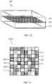
- FIG. 1Ais a schematic diagram of an optically variable device (OVD).
- OLEDoptically variable device
- FIG. 1Bis a schematic diagram of a plan view of a portion of the data storage layer of FIG. 1A .
- FIGS. 2A and 2Bare illustrations of an OVD, such as the OVD of FIG. 1A , operable to display an image and to store data using directional multiplexing
- FIG. 3is a schematic diagram of an OVD operable to store data and a printed image.
- FIG. 4is a schematic diagram of an OVD comprising diffractive structures with different profiles.
- FIGS. 5A and 5Bare schematic diagrams of an OVD comprising plasmonic structures.
- FIG. 6is a schematic diagram illustrating a biometric optical reader using nano-optical bit structures.
- FIG. 7is a schematic illustration of a data storage OVD with nano-optical bits arranged to represent an image.
- FIG. 8is a schematic diagram of a holographic-based nano-optical bit data storage device (OVD).
- FIG. 9is a schematic illustration of a holographic QR code.
- FIG. 10is a schematic illustration of an OVD comprising angle-multiplexed diffractive barcodes.
- FIG. 11is a schematic diagram of a multilayer OVD.
- FIG. 12is a schematic side view of a data storage layer comprising polymer encoded nano-optical bits.
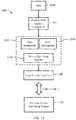
- FIG. 13is a block diagram illustrating a reader device system.
- FIG. 14Ais a schematic plan view of an implementation of an optical reader.
- FIG. 14Bis a schematic side view of the optical reader of FIG. 14A .
- FIG. 15is a schematic side view illustrating an example implementation of an optically variable storage device.
- FIG. 16is a schematic diagram illustrating an example implementation of a system for reading data from an OVD.
- FIG. 17is a schematic diagram illustrating an example implementation of a system that includes an OVD.
- FIG. 18is a flow diagram illustrating an example method of authentication using an OVD and a unique identifier.
- the technology described in this applicationcan increase the number of variables, and can provide a single integrated device that can combine overt data (such as a printed image) with covert, machine-readable data encoded with a high level of data security.
- FIG. 1Ais a schematic diagram of an embodiment of optically variable device (OVD) 100 .
- OVD 100comprises data storage layer 110 that uses a nano-optical bit system to store data.
- OVD 100further comprises upper layer 120 and lower layer 125 .
- Layers 120 and 125can comprises dielectric materials or metallic materials.
- OVD 100can comprise layers (not illustrated in FIG. 1A ) on the side of data storage layer 110 , in addition to, or instead of, layers 120 and 125 .
- Side layersextend in a plane orthogonal to upper and lower layers 120 and 125 .
- Layers 120 and 125 , and side layers if present,can provide a number of benefits including, but not limited to, the following:
- OVD 100comprises a series of diffraction gratings incorporated into layers 120 and/or 125 .
- the series of diffraction gratingscan be used to conceal the coded pattern, if desired.
- OVD 100is suitable for use as a data recording/storage medium for applications in which a large volume of data needs to be stored.
- the storage capacity of OVD 100can be increased by increasing the number of variables used in the nano-optical bit encoding system, and the number of values each variable can assume. For example, if two adjacent nano-optical bits in data storage layer 110 exhibit the same color, then the combination of two bits can be jointly represented by a new color.
- the storage capacity of OVD 100can also be increased by decreasing the size of the nano-optical bit structures. Increasing the data storage capacity increases the volume of data that can be stored within a given surface area.
- references to colorinclude wavelength and, more generally, spectral signature.
- FIG. 1Bis a schematic diagram of a plan view of portion 110 - 1 of data storage layer 110 of FIG. 1A .
- FIG. 1Billustrates the nano-optical bit encoding system.
- Pixels 130 through 137 of portion 110 - 1 of the data storage layercomprise diffractive structures encoding the data stored on OVD 100 .
- pixels 130 through 137would be represented by different colors such as red, blue, green, yellow and the like.
- the different pixels types, 130 through 137are shown with different shading patterns.
- FIGS. 2A and 2Bare illustrations of an OVD, such as OVD 100 of FIG. 1 , operable to display an image and to store data using directional multiplexing.
- FIGS. 2A and 2Billustrate the result of illuminating the surface of a data storage layer, such as data storage layer 110 of FIG. 1A .
- optically variable image 210is an image of a facsimile of a Canadian flag.
- FIG. 2Ais shown in black and white, optically variable image 210 comprises a color image.
- illumination of the surface of the data storage layer along the x-axis(as indicated by the arrow), in this particular example, reveals nano-optical bit structures 220 that can be used to store data.
- the OVD illustrated in FIGS. 2A and 2Bcomprises a combination of a diffractive image and a data recording system.
- the stored informationcan be visualized by angular multiplexing and using illumination at a predetermined direction and incidence angle.
- the OVDoperates in two or more directions, one direction dedicated to the stored data and the other directions used to store one or more diffractive images.
- the angle at which stored data is read from the nano-optical bitsis selected so that there is little or no interference from the structures comprising images visible by illuminating in other viewing directions.
- More data layerscan be added using multiplexing techniques to increase the data storage capacity of the OVD.
- adding multiplexing techniquescan include using multiple storage layers, each storage layer storing data in at least one direction.
- the data storage and the image(s)are on different layers, for example one layer comprising only stored data and another layer storing one or more diffractive images.
- the OVDprovides information from at least two viewing directions, as for example illustrated in FIGS. 2A and 2B in which the diffractive image and the encoded data are viewed from orthogonal directions.
- An OVDsuch as OVD 100 of FIG. 1
- a data storage layersuch as illustrated in FIGS. 2A and 2B
- the data storagecomprises machine-readable (i.e., coded) data.
- the OVDcan be used to provide both overt and covert information in a single device, such as an identification card. Overt information is provided via the image, for example, and is easy to authenticate. Covert information is machine-readable and can be secure.
- FIG. 3is a schematic diagram of an embodiment of OVD 300 operable to store data and a printed image.
- a multilayer OVDcan be constructed from two or more layers. In the embodiment illustrated in FIG. 3 , one layer acts as a medium to store data using nano-optical bits and another layer is a color (or monochromatic) printed image. The printed image can be a high resolution image.
- OVD 300comprises diffraction grating 310 , stored data layer 320 , and printed picture layer 325 .
- OVD 300further comprises layers 330 and 335 of dielectric or metallic materials that can provide the benefits described above in reference to FIG. 1A .
- the stored datacan be extracted while the image(s) on other layer(s) are invisible to an observer.
- the data storage layercan be replaced by one or more layers on which one or more diffractive images can be stored.
- Diffraction grating 310 placed above printed image layer 325can be used to cause a color change to the printed image in printed image layer 325 depending on the angle at which the printed image is being viewed. At one angle, the printed image can be viewed in true color (as it was originally printed). At other viewing angles, diffraction grating layer 310 causes the printed image to appear tinted in different colors such as the colors of the rainbow.
- printed image layer 325is below stored data layer 320 and diffraction layer 310 . In other implementations, printed image layer 325 can be above data storage layer 320 and/or diffractive image layer 310 .
- diffraction grating 310can be oriented such that it does not interfere with data storage layer 320 , and, at a selected angle, a reader can faithfully extract the colors for data storage layer 320 . In this configuration, diffraction grating 310 creates a rainbow effect for printed image layer 325 without affecting readout of data storage layer 320 .
- OVD 300can be configured so that a diffractive image can be viewed without interference.
- nano-optical bits 345can be readout from data storage layer 320 at viewing angle 340 .
- printed image 355can be observed from printed image layer 325 at viewing angle 350 .
- the layers of the OVDs described abovecan comprise transparent materials, semitransparent materials, wavelength-sensitive materials, photo sensitive materials, photo resists, conductive materials, semiconductor materials, dielectric materials, glass, piezoelectric materials, metalized, contain polarized elements, polymer based material, metallic, glossy paper, paper, and the like, or a suitable combination of the above.
- at least one protective layercomprising one or more materials from the above list is added to at least one side of the device, for example to the top of the device.
- the added layercomprises an anti-scratch coating intended to protect the surface of an adjacent layer.
- Encoding with nano-optical bitstakes advantage of spectral signatures (such as wavelengths and colors) to store information, and additional variables can be introduced based on the orientation of optical bits.
- intensity and polarizationcan be considered out-of-plane variables. Intensity and polarization variables can be modified and controlled in different ways.
- FIG. 4is a schematic diagram of OVD 400 comprising diffractive structures with different profiles.
- OVD 400can control and modify the intensity of nano-optical bits by using harmonic structures which are bits with integer multiples of the fundamental periodicities P of the bits (i.e., 2P, 3P . . . , and so on). These harmonic bit structures are capable of producing the same optical signal but with a lower intensity (with respect to the order of diffraction). The intensity can be measured and implemented as a variable.
- OVD 400comprises substrate 410 and regions 420 , 422 , 424 , and 426 comprising diffractive structures with different profiles.
- Region 420comprises diffractive structures with holes having a circular profile.
- Region 422comprises diffractive structures with a pyramid profile.
- Region 424comprises diffractive structures with a cuboid profile.
- Region 422comprises diffractive structures with a pillar profile.
- Periodic structures with different profiles and shapescan exhibit diffraction with different intensities.
- regions 420 , 422 , 424 , and 426exhibit diffraction at intensities indicated by the height of arrows 430 , 432 , 434 , and 436 , respectively.
- Other suitable shapes and/or profilescan be used.
- structures with more edgesdiffract light with higher intensity.
- nano-optical bits with the same, or similar, spacing in the diffractive structurecan produce optical signals with different intensities.
- adjusting the profile of the nano-structures, without changing the spacing (periodicity)will result in differences in intensity between optical bits with the same, or similar, spacing.
- the optical reader for OVD 400comprises a meter for determining the intensity of refracted light, in addition to a sensor for detecting different colors.
- structures operable to exhibit different intensities in the diffracted lightcomprise holes or indentations in substrate 410 . In other implementations, structures operable to exhibit different intensities in the diffracted light comprise different materials and/or different thicknesses of materials.
- polarization of the transmitted or reflected beamcan be used as a variable for encoding the stored data.
- Each nano-optical bitcan comprise polarizing structures that polarize the beam.
- nano-optical bit data storage systemcan include both polarization and intensity as variables for representing and encoding the stored data.
- the shape of the optical bitscan also be used as a variable. For instance, a portion of the bits can be presented in square shapes while another portion of the bit shapes can be presented in circles, triangles, hexagons and other suitable geometrical shapes.
- Each nano-optical bitcan be designed to produce the same optical signal while differing in shape and size where each parameter is adding an extra variable to the data storage system creating a more complex and secure environment for the stored data.
- the aforementioned variablescan be incorporated in an OVD as described above.
- the OVDis operable to store and represent different types of data including, but not limited to, image files (for example JPEG, TIFF, and GIFF), audio files (for example MP3, and WAV), video files (for example MP4, and MPEG), text files (for example txt, doc, and PDF), and binary files.
- a data storage OVDsuch as OVDs described above in references to FIGS. 1 through 4 is suitable for storing large amounts of data in one or more formats, and in particular is suitable for storing data in applications where network connectivity is not an option. Authentication can be performed offline.
- the nano-optical bits of a data storage OVDcan be constructed from plasmonic structures. Arrays of plasmonic bits can be used for data storage, and this approach can be incorporated in the OVDs described in this application.
- Plasmonic structurescan generate surface plasmon once embedded or coated with suitable conductive materials such as gold, silver, aluminum, conductive polymers, and the like.
- suitable conductive materialssuch as gold, silver, aluminum, conductive polymers, and the like.
- the peak of plasmonic resonance in transmission or reflectioncan be detected and used for data representation and storage.
- the plasmonic peakcan be controlled by selecting the periodicity of the bits, the type and profile of the constituent nano-structures, the materials used for coating or embedding the structures and their thickness, and the type and thickness of the dielectric layer or layers that surround and cover the plasmonic structures.
- FIGS. 5A and 5Bare schematic illustrations of an embodiment of OVD 500 comprising plasmonic structures.
- OVD 500comprises data storage layer 510 , and two secondary layers, upper layer 520 and lower layer 525 , above and below data storage layer 510 , respectively.
- Layer 510comprises plasmonic structures.
- Layers 520 and 525comprises dielectric or metallic materials.
- FIG. 5Bis a plan view of OVD 500 illustrating the nano-optical bits such as 530 a through 536 a , and 530 b through 536 b .
- the nano-optical bitscomprise arrays of plasmonic structures with different periodicities.
- the periodicity of each arrayis selected to represent data using a multi-variable encoding system.
- Datais encoded in colors and each periodicity results in a different color.
- the pattern of colorsencodes the data stored in OVD 500 .
- bits 530 a and 530 bcomprise a first periodicity
- bits 532 a and 532 bcomprise a second periodicity
- bits 534 a and 534 bcomprise a third periodicity
- bits 536 a and 536 bcomprise a fourth periodicity.
- an optical reader(not shown in FIGS. 5A and 5B ) to read out the data stored in data storage layer 510 of OVD 500 can comprise two sensors, a diffraction sensor and a transmission (and/or reflection) sensor.
- the diffraction sensorcan read out the data.
- the transmission (and/or reflection) sensorcan provide additional security. It can be beneficial to have a combination of diffraction and transmission (and/or reflection) sensors.
- An OVD with a data storage componentcan be used for creating a hash file using biometric features such as fingerprints, retinal scans, and the like.
- a pattern of nanostructures, containing either information or a random pattern,can generate a unique optical signal, when illuminated.
- a unique signalcan be recorded, the unique signal comprising a convolution of the biometric feature and the optical signature of the nano-optical pattern.
- the convolutionis unique to the specific combination of the biometric feature and the nano-optical pattern, and can be used to create a hash file in real-time.
- the unique signal(the combination of the biometric feature and the nano-optical pattern) can be stored in a database, and subsequently used to verify the authenticity of a person, for example a person in possession of an identification card or document.
- the technique for authentication described abovecan be used to link an item (such as an identification card, a travel document, and the like) to an appropriate individual.
- the techniquereduces or eliminates the possibility that personal identification features, such as biometrics, recorded by a device can be captured and/or hacked.
- biometricsare not recorded, and the generated optical pattern is a convolution of the biometrics and the pattern of nano-structures, and cannot be broken down by a third party into its constituents.
- FIG. 6is a schematic diagram illustrating an embodiment of a biometric optical reader 600 using nano-optical bit structures.
- Biometric optical reader 600comprises transparent platform 610 , coded structure 620 , and transparent substrate 630 .
- coded structure 620coded structure 620
- transparent substrate 630transparent substrate 630 .
- biometric optical reader 600produces modulated beam 655 .
- Modulated beam 655comprises a representation of a fingerprint corresponding to finger 640 and a pattern derived from coded structure 620 .
- modulated beam 655is a convolution of the fingerprint and the pattern derived from coded structure 620 .
- Modulated beam 655is secure i.e., the fingerprint cannot be deduced from modulated beam 655 without knowledge of a decoding algorithm corresponding to coded structure 620 .
- Nano-optical bits in an OVDcan be selectively and physically arranged in a pattern to represent a recognizable image. Since the nano-optical bits are operable to record a specific color, the recognizable image can simultaneously be an optically variable image i.e., an image for storing coded data. The data is stored in the arrangement of colored bits. A corresponding method can be used to decode the data.
- a benefit of the encoding system described aboveis that it is difficult, if not impossible, to decode the data without knowledge of the decoding method and the angle at which to view the data to detect the encoded image.
- the decoding methodcan be implemented in an embedded chip without passing through a digital interface.
- the chipcan be protected against discovery by being operable to burn-out if an attempt is made to compromise it. Further protection can be provided by requiring authentication for a user or for software accessing data received from the chip.
- FIG. 7is a schematic illustration of a data storage OVD 700 with nano-optical bits arranged to represent an image.
- FIG. 7shows portion 710 of OVD 700 expanded to highlight nano-optical bits including bits 720 , 722 , 724 , and 726 .
- bits 720 , 722 , 724 , and 726would be represented by different colors such as red, green, blue, and yellow.
- the nano-optical bitsare arranged to display a facsimile of a Canadian flag while, at the same time, representing data in a multi-variable encoding system.
- a nano-optical bit storage devicecan also take advantage of transmissive nano-structures to store and represent data using a laser beam.
- the diffraction pattern of the arrays of nano-structurescan be stored on a film, for example holographic film or a photopolymer, similar to recording a hologram.
- Arrays of nano-optical bitsare used to modulate the laser beam.
- Angle multiplexingcan be used to increase data density i.e., to store more data in a given area of the device.
- the number of bitsis dependent on the number of nano-arrays used to store the data.
- FIG. 8is a schematic diagram of a holographic-based nano-optical bit data storage device (OVD) 800 .
- Holographic OVD 800comprises laser 810 , lenses 820 , 822 , and 824 , beam splitter 830 , reflector 840 , nano-optical bit array 850 - 1 , and holographic film 860 .
- Beam B 1 from laser 810is split into two beams B 2 and B 3 after passing through beam splitter 830 .
- Beam B 2passes through nano-optical bit array 850 - 1 .
- Nano-optical bit array 850 - 1comprises a diffraction grating with a first periodicity.
- Beam B 2is modulated by transmission through nano-optical bit array 850 - 1 to form modulated beam B 4 .
- Modulated beam B 4is incident on holographic film 860 .
- Reference beam B 5is co-incident with modulated beam B 3 on holographic film 860 , i.e., beams B 4 and B 5 are incident on the same region 870 of holographic film 860 at the same time.
- Each of the arrays of nano-structuresis representing a nano-optical bit which is being recorded on the film.
- Each arrayis a variable that can be used to represent stored data. To store data using these arrays, the method illustrated in FIG. 8 records the interference pattern for each array.
- Angle multiplexingcan be used to store more than one pattern in a region of holographic film.
- the angle of the reference beamcan be kept fixed and interference patterns recorded across the film for diffracted light from each array.
- a combination of the two methodscan be used.
- the methodcan include moving reflector 840 to adjust the angle of incidence of the reference beam on the holographic film.
- the reference beamhas an angle ⁇ 1 with a line normal to the plane of the holographic film at the incidence point on the holographic film.
- the methodrecords an interference pattern between modulated beam B 4 and reference beam B 5 , reference beam B 5 incident at an angle ⁇ 1 .
- the reference beamhas an angle ⁇ 2 with a line normal to the plane of the holographic film at the same incidence point on the holographic film.
- the interference pattern of reference beam B 5 and modulated beam B 4is recorded on the same region of the holographic film as for the nano-structure with periodicity P1, this time with a reference beam angle of ⁇ 2 .
- one or more patternscan be stored on the same region of the holographic film for a corresponding set of one or more reference beam angles.
- HCDHolographic Versatile Discs
- Reference beam B 5is used to illuminate region 870 of holographic film 860 at a selected angle to extract modulated beam B 4 .
- Modulated beam B 4can be detected by a conventional CMOS or a CCD sensor.
- the datacan be readout by detecting the color exhibited by the recorded interference pattern.
- a combination of this approach and the approach described in the previous paragraphcan be used to readout the data.
- the technique described aboveis suitable for recording small or large volumes of data, and can be adjusted accordingly.
- the readout devicecan be a dedicated optical reader or a sensor in an electronic device such as a cell-phone. If the data is recorded in 3D (i.e., with more than one pattern in the same region of the holographic film, the data layer extending into the film material), then a designated reading device is used for data extraction. If the data is recorded in 2D (one pattern per spot, the data layer residing on the surface of the film material) then the same cell-phone based color combination method can be used for decrypting the data.
- the number of variablescan be increased by adding more nano-arrays.
- An angular multiplexing technique to record multiple optical bit patterns on the same region of the holographic filmcan be used to increase data storage capacity.
- the region of holographic film on which the recording is madeis defined by a lens system comprising lenses 820 , 822 , and 824 , and laser 810 .
- the regioncan be adjusted by suitable selection of lenses 820 , 822 , and 824 , and the type of laser 810 used to provide the light source.
- a data storage device produced as described abovecan be used as a standalone storage medium and/or can be incorporated in OVDs described in this application.
- a multivariable optical storage devicecan use semiconductor nano-crystals as nano-optical bits.
- Semiconductor nano-crystalsare also known as quantum dots (QDs).
- QD inkswhich are commercially available and used in the security industry, can be used to represent data on wide range of materials.
- QDsare capable of emitting light when excited, for example by irradiation with UV light, electrical current, heat, and the like.
- the emitted wavelengthdepends on the size of the nano-crystals.
- a QD-based multivariable storage deviceexploits the variation of emitted wavelength with size of the nano-crystals. Data can be stored as nano-crystals of varying sizes and the data can be read out by detecting the wavelengths emitted by the QDs after excitation. Data can be extracted using a decoding method while the QDs are excited.
- a fluorescent or phosphorescent pigment or inkcan be used to represent information in a similar fashion.
- upconverting nano-particles and plasmonic nano-particlescan be made into ink, and printed onto documents.
- the inkcan be used to print the multivariable encoding system described above.
- the printed outputcan comprise pixels made of nano-particles such as QDs, upconverting nano-particles and plasmonic nano-particles.
- the inkcan be used to print a barcode.
- Upconverting nano-particlescan absorb infra-red (IR) and near IR (NIR) radiation and re-emit it in the visible spectrum.
- An IR or NIR sourceexcites and reads data stored in upconverting nano-particles.
- Plasmonic nano-particlescan be made in different sizes and shapes, size and shape being used to control color, and color being used to encode the data. Plasmonic nano-particles exhibit a color-shift effect through dispersion of incident light.
- a data storage device produced as described abovecan be used as a standalone storage medium and/or can be incorporated in OVDs described in this application.
- one or more barcodessuch as QR codes can be used to produce an OVD.
- QR codescan be used to produce an OVD.
- a combination of barcodescan be used to provide multiplexing as described in more detail below.
- the modules of the barcode(for example, each of the black or white blocks in a QR code) can be made of diffractive structures with periodicities ranging from nanometer to micrometer in size.
- the resultis a barcode in which the barcode modules that represent the encoded data are selected to exhibit a color-shift effect similar to holograms.
- the color-shift effectrefers to a diffraction effect similar to the effect of diffractive images described above.
- the barcode moduleschange color when tilted under illumination.
- the barcode OVDcan be read by a barcode reader such as a QR code reader on a smartphone.
- FIG. 9is a schematic illustration of holographic QR code 910 .
- FIG. 9also shows an expanded view of a portion of QR code 910 comprising single diffractive module 920 .
- FIG. 9also shows an expanded view of diffractive module 920 , the view showing diffraction grating 930 .
- Barcodes as described abovecontain a high level of security since they cannot be produced by a conventional 2D printer. They can be imprinted in or onto a wide variety of materials as mentioned earlier.
- barcodes comprising diffractive nano-structurescan be generated using a 3D printing technology.
- FIG. 10is a schematic illustration of OVD 1000 comprising angle-multiplexed diffractive barcodes.
- OVD 1000comprises two QR code layers 1010 and 1015 for data storage.
- OVD 1000further comprises two substrate layers 1020 and 1025 .
- FIG. 10illustrates an example with two data storage layers, other implementations can comprises more than two data storage layers.
- Barcode modulescan also be populated with nano-optical bits and used to store data that can be read by an electronic device such as a cellphone or a special-purpose device.
- the security barcode system described above in reference to FIGS. 9 and 10can be incorporated in OVDs, methods, and materials described in this application.
- datais stored in different layers of polymers, each polymer having a characteristic refractive index, and the different layers having a different refractive indices.
- the approachallows coded patterns in the nano-structures to be viewed in different positions by virtue of the difference in the refractive indices.
- FIG. 11is a schematic diagram of an embodiment of a multilayer OVD 1100 .
- Multilayer OVD 1100comprises three stored data layers 1110 , 1112 , and 1114 on top of three substrate layers 1120 , 1122 , and 1124 , respectively. In operation, multilayer OVD 1100 is illuminated by light beam 1130 .
- a patch of a polymercan be applied over a diffractive structure.
- the polymercan be selected to have a characteristic refractive index. More than one polymer can be applied, one polymer per diffractive structure, each of the polymers selected to have a characteristic refractive index that can be varied from one polymer to another.
- the resulting OVDcomprises diffraction structures with a periodicity in common with each other, and a refractive index that can vary from one diffraction structure to another.
- the varying refractive indexcan result in a shift in the color recorded when reading out the OVD at a particular fixed viewing angle.
- datacan be encoded in the colors corresponding to the diffraction structures (or bits).
- the encodingcan be achieved by applying polymers to the bits, the polymers having appropriately selected characteristic refractive indices to provide a desired color.
- the periodicity of the diffraction structure and the refractive index of the polymercan both be varied between bits.
- FIG. 12is a schematic side view of data storage layer 1200 comprising polymer encoded nano-optical bits.
- Data storage layer 1200comprises regions 1210 , 1212 , 1214 , and 1216 , each region comprising a diffraction region coated with a polymer having a selected characteristic refractive index.
- the normal to the diffraction structures in regions 1210 , 1212 , 1214 , and 1216are 1220 , 1222 , 1224 , and 1226 , respectively.
- OVD 1200is illuminated by light 1230 .
- Light 1230reflects at different angles for each color as indicated by sets of arrows 1240 , 1242 , 1244 , and 1246 , respectively.
- the presence of the polymer coating on the diffraction gratingchanges the perceived color at a given viewing angle.
- the OVDs described abovecan be fabricated using conventional micro/nano-fabrication techniques and devices such as electron-beam lithography, ion-beam lithography, focused-ion beam, nano-imprint lithography, roll to roll, hand casting, hot embossing, photolithography, deep UV lithography, laser interference lithography, maskless lithography, and the like.
- Different layers of multilayer OVDscan be applied using spin-coating, spray-coating, hot press or other standard or unconventional techniques, and the layers can be stacked on top of each other.
- OVDs described abovecan be used for a range of applications with requirements including, but not limited to, the following:
- applicationsinclude, but are not limited to, the following:
- FIG. 13is a block diagram illustrating an embodiment of reader device system 1300 .
- System 1300comprises OVD 1310 , optical capture subsystem 1320 , optical data interpreter 1332 , data decryption subsystem 1334 , and device operating system 1336 .
- OVD 1310comprises encrypted data as described in previous paragraphs with references to FIGS. 1 through 12 .
- Optical capture subsystem 1320comprises an optical system that captures data from OVD 1310 using a predetermined viewing direction and angle of incidence.
- Optical data interpreter 1332comprises a microcontroller. In one implementation, optical data interpreter 1332 comprises an application specific integrated circuit (ASIC) operable to transform captured optical data into numerical data.
- ASICapplication specific integrated circuit
- Data decryption subsystem 1334comprises a data decryption secure microcontroller, which is an ASIC that contains the specific functions and algorithms for decrypting the numerical data.
- ASICdata decryption secure microcontroller
- the term “secure”defines the structure of the ASIC in such way that attempts at reverse engineering the ASIC through accessing the firmware will result in physical burn-out of the interface gates. Consequently, the ASIC's functionality cannot be accessed through its embedded software.
- the ASICcomprises cryptographic machine code that hides the ASIC's actual functionality.
- System 1300further comprises data transfer interface 1340 and external device operating system 1350 .
- Authentication of OVD 1310is performed between data transfer interface 1340 and external device operating system 1350 .
- FIG. 14Ais a schematic plan view of an example implementation of optical reader 1400 .
- FIG. 14Bis a schematic side view of optical reader 1400 of FIG. 14A .
- Optical reader 1400can be used to read OVD 1410 incorporated for example on a card or document.
- Optical reader 1400comprises body 1420 , rails 1430 and 1435 , collimated light source 1440 , and detector 1450 .
- Optical readerfurther comprises platform 1460 .
- OVD 1410can be placed on platform 1460 or inserted into optical reader 1400 through a slot (not shown in FIGS. 14A and 14B ).
- Optical reader 1400is an example embodiment. Other suitable embodiments and methods can be used to read out OVDs, including OVDs described above. Optical 1400 detects light reflected by diffraction gratings in OVD 1410 . In some embodiments, for example, with a suitable selection of transparent substrate materials, the colors encoding the data can be detected in light transmitted through OVD 1410 .
- datacan be encoded in colors for different angles of incidence, for different angles of diffraction (also referred to as viewing angles), and/or for a combination of angles of incidence and diffraction for a subset of one or more diffractive structures in an array of one or more diffractive structures.
- OVD 100can comprise data storage layer 110 .
- data storage layer 110can use a nano-optical bit system to store data.
- FIG. 1Billustrates portion 110 - 1 of data storage layer 110 .
- portion 110 - 1 of data storage layer 110includes pixels 130 through 137 that comprise diffractive structures encoding data stored on OVD 100 .
- pixels 130 through 137 of FIG. 1Bcould be represented by different colors such as red, blue, green, yellow and the like.
- FIG. 1Bthe different pixels types, 130 through 137 , are shown with different shading patterns.
- FIG. 15is a schematic diagram illustrating an example implementation of optically variable storage device 1500 .
- optically variable storage device 1500can include data storage layer 1502 .
- data storage layercan include an array of one or more diffractive structures 1504 .
- One or more colorscan be encoded in diffractive structure 1504 , illuminated by an optical source at an angle of incidence, and selectively readable at one or more viewing angles. For example, at viewing angle 1506 a , diffractive structure 1504 encodes a color 1508 a , at viewing angle 1506 b , diffractive structure 1504 encodes a color 1508 b , and at viewing angle 1506 c , diffractive structure 1504 encodes a color 1508 c.
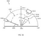
- FIG. 16is a schematic diagram illustrating an example implementation of system 1600 for reading data from an OVD (for example, OVD 100 of FIGS. 1A and 1B ).
- OVDfor example, OVD 100 of FIGS. 1A and 1B .
- system 1600includes optical source 1604 (also referred to as a light source and/or an optical light source).
- optical source 1604can be a polychromatic source.
- optical source 1604can be a monochromatic source.
- optical source 1604can be a laser.
- optical source 1604can illuminate a surface of OVD 1602 at angle of incidence 1606 to the surface of OVD 1602 measured from normal 1612 to the surface of OVD 1602 .
- angle of incidence 1606can be varied, for example from 0° to 90°. In some embodiments, angle of incidence 1606 is fixed during an operation to read OVD 1602 .
- angle of incidence 1606varies during an operation to read OVD 1602 . In some embodiments, angle of incidence 1606 is changed between one operation to read OVD 1602 and another operation to read OVD 1602 .
- optical source 1604can move along path 1614 . In some implementations, path 1614 can lie on a hemisphere with a center at least approximately coincident with OVD 1602 . In some implementations, OVD 1602 is at an eccentric position with respect to optical source 1604 . In some implementations, optical source 1604 is a plurality of physical sources that can move independently of one another and/or in concert.
- system 1600includes optical capturing device 1614 .
- optical capturing device 1614can record light 1616 refracted from the surface of OVD 1602 .
- optical capturing device 1614can record a color (often referred to as a spectrum and/or a spectral signature).
- a position and look direction of optical capturing device 1614can be controlled and/or adjusted.
- optical capturing device 1614can vary with angle of incidence 1610 .
- optical capturing device 1614can move in response to a movement of optical source 1604 .
- optical capturing device 1614can move independently of optical source 1604 .
- optical capturing devicecan move along path 1614 .
- optical capturing device 1614can include a device able to learn which angles of incidence may contain readable data.
- the devicecan cause optical capturing device 1614 to capture diffracted light from OVD 1602 according to one or more instructions (also referred to as commands) from a computing device.
- the computing deviceis a back-end server.
- the color of light diffracted from OVD 1602 in response to illumination by optical source 1602can vary with angle of incidence 1610 and angle of diffraction 1620 .
- optical capturing device 1614can capture one or more colors and/or one or more angles of incidence 1610 and angles of diffraction 1620 .
- optical capturing device 1614can optionally record one or more colors.
- optical capturing device 1614captures each of a defined set of colors at a respective angle of incidence 1610 and angle of diffraction 1620 .
- optical capturing device 1614transmits a recorded set of colors to a decoder.
- the computing deviceincludes the decoder.
- an optical bitincludes more than one diffractive structure, for example an array of diffractive structures.
- two-dimensional encodingcan be used in which two variables are employed to encode data in the optical bit.
- color and positioncan be employed as variables.
- an address to a diffractive structure in the arraycan be employed as a variable in addition to a color.
- color RED at position (n,m)can encode a different value color RED at position (n+1, m).
- the systems and methods describedinclude an array of N diffractive structures for encoding colors to represent data in an optically variable storage device.
- more than one colorcan be encoded in the single diffractive structure by constructing the single diffractive structure to diffract one defined color at a defined viewing angle and for a defined angle of incidence of illumination from an optical source (for example optical source 1602 of FIG. 16 ), and another color at a different viewing angle and/or for a different angle of incidence of illumination from an optical source.
- FIG. 17is a schematic diagram illustrating an example implementation of system 1700 that includes OVD 1702 .
- OVD 1702can be one of the embodiments or implementations of an OVD described in the present application, or another suitable OVD.
- System 1700includes device 1704 that includes OVD 1702 and unique identifier 1706 (UID).
- UID 1706can include one or more of the following a) a serial number, a shape and/or an image, etc. which can be, among other things, etched into a surface of device 1704 , printed onto a surface of device 1704 , carved in a surface of device 1704 , and/or embossed on a surface of device 1704 ; b) a RFID (radio frequency identification); c) a barcode; d) a tag that includes one or more optical bits (in some example implementations, the optical bits in the UID tag are at a lower density than in an OVD); e) a chip that uses a PIN (personal identification number); and/or f) one or more biometrics (for example, fingerprint data, retinal data, facial recognition data, voice recognition data, etc.).
- biometricsfor example, fingerprint data, retinal data, facial recognition data, voice recognition data, etc.
- system 1700includes sensing system 1708 .
- sensing system 1708can include a UID sensor to acquire a UID, for example by means of a signal such as an RF signal in the example of an RFID.
- sensing system 1708can include an optical reader.
- Optical readercan be configured to read OVD 1702 , for example.
- sensing system 1708can include a software application (also referred to herein as a reader application).
- system 1700includes computing system 1710 .
- computing system 1710is a server.
- computing system 1710is a backend.
- computing system 1710includes database 1712 .
- computing system 1710is communicably coupled to sensing system 1708 by one or more data networks 1714 .
- computing system 1710 and sensing system 1708communicate via an application programming interface (API).
- APIapplication programming interface
- computing system 1710is a cloud computing system. In some embodiments, computing system 1710 is in the cloud.
- database 1712can differentiate between different devices such as device 1704 .
- database 1712can identify device 1704 using UID 1706 .
- computing system 1710can learn about device 1704 , and can transmit one or more sets of instructions to sensing system 1708 via one or more data networks 1714 .
- database 1712can store one or more color combinations associated with UID 1706 .
- OVD 1702can store data encrypted using colors (or spectral signatures).
- data related to device 1704can only be extracted when UID data, data stored on OVD 1702 , and related data stored in database 1712 are available.
- data related to device 1704can only be extracted when UID data, data stored on OVD 1702 , and related data stored in database 1712 match.
- system 1700can include an authentication system. Authentication can include authenticating UID data and OVD data using data stored in database 1712 . In some embodiments, system 1700 can perform authentication by decryption of data stored (or encoded) in OVD 1702 . In some embodiments, system 1700 can perform authentication by using a combination of data from UID 1706 , data stored (or encoded) in OVD 1702 , and/or data stored in database 1712 .
- one advantage of the systems and methods describedis that data can be encrypted on a device such as device 1704 .
- another advantageis that the amount of data associated with the device can be less limited.
- FIG. 18is a flow diagram illustrating example method 1800 of authentication using an OVD and a UID.
- Method 1800includes acts 1802 through 1808 .
- method 1800may include other acts, and/or may omit one or more of acts 1802 through 1808 .
- Method 1800describes a method of operation of a system (for example, system 1700 of FIG. 17 ).
- the systemtransmits UID data from a device (for example, device 1704 of FIG. 17 ) to a computing system (for example, computing system 1710 of FIG. 17 ).
- the computing systemis also referred to in reference to FIG. 18 as a backend.
- the systemtransmits instructions from the backend to an optical reader.
- the instructionscan include color combinations, illumination angles, diffraction angles, and/or the like.
- the instructionscan be used to read data (for example, encoded or encrypted data) from an OVD (for example, OVD 1702 of FIG. 17 ).
- the systemtransmits optical data to the backend for decryption. In some embodiments, at 1808 , the system transmits a decryption result to the optical reader.
- OVDsand their associated methods and materials, described above and in reference to FIG. 1 through FIG. 18 can be used individually or in various suitable combinations.
Landscapes
- Physics & Mathematics (AREA)
- Engineering & Computer Science (AREA)
- General Physics & Mathematics (AREA)
- Theoretical Computer Science (AREA)
- Electromagnetism (AREA)
- Health & Medical Sciences (AREA)
- General Health & Medical Sciences (AREA)
- Toxicology (AREA)
- Artificial Intelligence (AREA)
- Computer Vision & Pattern Recognition (AREA)
- Nanotechnology (AREA)
- Chemical & Material Sciences (AREA)
- Diffracting Gratings Or Hologram Optical Elements (AREA)
- Credit Cards Or The Like (AREA)
- Holo Graphy (AREA)
Abstract
Description
- acting as protective layers,
- enhancing the brightness,
- concealing a coded pattern, and
- changing the optical path (depending on the refractive indices of the materials that are used).
- a high level of security for data storage,
- the storing of sensitive data for a long period of time,
- the authentication of an item,
- archiving high value information,
- brand protection,
- physically unclonable unique object functions, and
- tracking of items.
- access management for high security facilities,
- government regulated products, security and authentication,
- security conscious organizations, and
- pharmaceutical applications, and
- other suitable applications in which OVDs can be used.
Reader Device System
Claims (18)
Priority Applications (1)
| Application Number | Priority Date | Filing Date | Title |
|---|---|---|---|
| US16/133,210US11126902B2 (en) | 2014-06-03 | 2018-09-17 | Optically variable data storage device |
Applications Claiming Priority (4)
| Application Number | Priority Date | Filing Date | Title |
|---|---|---|---|
| US201462007338P | 2014-06-03 | 2014-06-03 | |
| US14/727,865US9489604B2 (en) | 2014-06-03 | 2015-06-02 | Optically variable data storage device |
| US15/289,916US10102462B2 (en) | 2014-06-03 | 2016-10-10 | Optically variable data storage device |
| US16/133,210US11126902B2 (en) | 2014-06-03 | 2018-09-17 | Optically variable data storage device |
Related Parent Applications (1)
| Application Number | Title | Priority Date | Filing Date |
|---|---|---|---|
| US15/289,916Continuation-In-PartUS10102462B2 (en) | 2014-06-03 | 2016-10-10 | Optically variable data storage device |
Publications (2)
| Publication Number | Publication Date |
|---|---|
| US20190034773A1 US20190034773A1 (en) | 2019-01-31 |
| US11126902B2true US11126902B2 (en) | 2021-09-21 |
Family
ID=65038654
Family Applications (1)
| Application Number | Title | Priority Date | Filing Date |
|---|---|---|---|
| US16/133,210Active2035-11-25US11126902B2 (en) | 2014-06-03 | 2018-09-17 | Optically variable data storage device |
Country Status (1)
| Country | Link |
|---|---|
| US (1) | US11126902B2 (en) |
Families Citing this family (9)
| Publication number | Priority date | Publication date | Assignee | Title |
|---|---|---|---|---|
| ES2718528T3 (en)* | 2013-11-07 | 2019-07-02 | Scantrust Sa | Two-dimensional barcode and authentication procedure of said barcode |
| US11126902B2 (en)* | 2014-06-03 | 2021-09-21 | IE-9 Technology Corp. | Optically variable data storage device |
| WO2016121210A1 (en)* | 2015-01-26 | 2016-08-04 | 凸版印刷株式会社 | Identification device, identification method, identification program, and computer-readable medium containing identification program |
| WO2017094761A1 (en)* | 2015-11-30 | 2017-06-08 | 凸版印刷株式会社 | Identification method and identification medium |
| JP6947166B2 (en)* | 2016-03-23 | 2021-10-13 | ソニーグループ株式会社 | Information processing device and information processing method |
| US10586135B2 (en)* | 2017-06-16 | 2020-03-10 | University Of Florida Research Foundation, Incorporated | Nano-electro-mechanical labels and encoder |
| EP3786848A1 (en)* | 2019-08-30 | 2021-03-03 | Authentic Vision GmbH | Object marking, production and authentication method |
| CN114341874B (en)* | 2019-08-30 | 2025-02-07 | 真视野股份有限公司 | Object marking, generation and authentication methods |
| US12265874B2 (en)* | 2019-11-26 | 2025-04-01 | Avery Dennison Retail Information Services Llc | RFID devices including embossed or other elements |
Citations (126)
| Publication number | Priority date | Publication date | Assignee | Title |
|---|---|---|---|---|
| US4721217A (en) | 1986-08-07 | 1988-01-26 | Optical Coating Laboratory, Inc. | Tamper evident optically variable device and article utilizing the same |
| US4765656A (en) | 1985-10-15 | 1988-08-23 | Gao Gesellschaft Fur Automation Und Organisation Mbh | Data carrier having an optical authenticity feature and methods for producing and testing said data carrier |
| US5101184A (en) | 1988-09-30 | 1992-03-31 | Lgz Landis & Gyr Zug Ag | Diffraction element and optical machine-reading device |
| WO1993018419A1 (en) | 1992-03-12 | 1993-09-16 | Commonwealth Scientific And Industrial Research Organisation | Security diffraction grating with special optical effects |
| US5461239A (en)* | 1991-06-05 | 1995-10-24 | Mikoh Pty Ltd | Method and apparatus for coding and reading information in diffraction gratings using the divergence of diffracted light beams |
| US5549953A (en) | 1993-04-29 | 1996-08-27 | National Research Council Of Canada | Optical recording media having optically-variable security properties |
| US5591527A (en) | 1994-11-02 | 1997-01-07 | Minnesota Mining And Manufacturing Company | Optical security articles and methods for making same |
| US5621515A (en) | 1994-01-25 | 1997-04-15 | Nhk Spring Co., Ltd. | Identification system using regions of predetermined properties interspersed among regions of other properties |
| US5786910A (en) | 1995-05-11 | 1998-07-28 | Advanced Deposition Technologies, Inc. | Pattern metallized optical varying security devices |
| EP0858056A2 (en) | 1997-01-10 | 1998-08-12 | BUNDESDRUCKEREI GmbH | Data carrier |
| US5811775A (en)* | 1993-04-06 | 1998-09-22 | Commonwealth Scientific And Industrial Research Organisation | Optical data element including a diffraction zone with a multiplicity of diffraction gratings |
| US5856048A (en) | 1992-07-27 | 1999-01-05 | Dai Nippon Printing Co., Ltd. | Information-recorded media and methods for reading the information |
| EP0490923B1 (en) | 1989-09-04 | 1999-02-03 | Commonwealth Scientific And Industrial Research Organisation | Diffraction grating and method of manufacture |
| US6043936A (en) | 1995-12-06 | 2000-03-28 | De La Rue International Limited | Diffractive structure on inclined facets |
| US6052354A (en) | 1995-06-23 | 2000-04-18 | Thin Film Electronics Asa | Optical data storage medium and method for writing and reading of data |
| US6060143A (en)* | 1996-11-14 | 2000-05-09 | Ovd Kinegram Ag | Optical information carrier |
| US20010005570A1 (en)* | 1994-05-04 | 2001-06-28 | Francoise Daniel | Multi-layer assembly and method for marking articles and resulting marked articles |
| US20010013830A1 (en)* | 1998-08-14 | 2001-08-16 | 3M Innovative Properties Company | Applications for radio frequency identification systems |
| US20010043396A1 (en) | 1998-07-02 | 2001-11-22 | Lee Robert Arthur | Diffractive structure with interstitial elements |
| WO2002000445A1 (en) | 2000-06-28 | 2002-01-03 | De La Rue International Limited | Optically variable security device |
| US6342969B1 (en) | 1993-05-25 | 2002-01-29 | Commonwealth Scientific/Industrial Research Organization | Multiple image diffractive device |
| US6343745B1 (en)* | 1996-12-06 | 2002-02-05 | Giesecke & Devrient Gmbh | Security device |
| US20020021445A1 (en) | 2000-07-21 | 2002-02-21 | Sergey Bozhevolnyi | Surface plasmon polariton band gap structures |
| US20020030360A1 (en) | 1993-10-13 | 2002-03-14 | Jurgen Herrmann | Value-bearing document with window |
| US20020071076A1 (en)* | 2000-08-16 | 2002-06-13 | Webb Richard M. | Scannable barcode display and methods for using the same |
| EP0690923B1 (en) | 1993-03-12 | 2002-07-03 | Colifast AS | Rapid coliform detection system |
| US20020145037A1 (en)* | 2001-04-09 | 2002-10-10 | Goodwin John C. | Item processing device with barcode reader and integrated RFID interrogator |
| US6502757B1 (en) | 1999-09-17 | 2003-01-07 | Dai Nippon Printing Co., Ltd. | Information recorded medium, device for reading the information, information recorded medium transfer foil, and method for producing information recorded medium |
| US20030010830A1 (en) | 2001-06-27 | 2003-01-16 | Curtis Kevin R. | Holographic card formats for presentation and security |
| US20030035539A1 (en)* | 2001-08-17 | 2003-02-20 | Thaxton Daniel D. | System and method for distributing secure documents |
| US20030039195A1 (en) | 2001-08-07 | 2003-02-27 | Long Michael D. | System and method for encoding and decoding an image or document and document encoded thereby |
| US20030042487A1 (en) | 2001-04-25 | 2003-03-06 | Sarychev Andrey K. | Plasmonic nanophotonics methods, materials, and apparatuses |
| US20030095416A1 (en) | 2001-10-24 | 2003-05-22 | Huizenga David J. | Vehicle handle assembly with cup lighting |
| US20030155495A1 (en) | 2000-07-03 | 2003-08-21 | John Drinkwater | Device with anti-counterfeiting diffractive structure |
| US20030157305A1 (en) | 2000-06-21 | 2003-08-21 | Abraham Nigel Christopher | Optical encoding |
| US20030174373A1 (en) | 2000-07-03 | 2003-09-18 | John Drinkwater | Optical device |
| US20030179364A1 (en) | 2002-01-24 | 2003-09-25 | Nanoventions, Inc. | Micro-optics for article identification |
| US20040100707A1 (en) | 2000-06-28 | 2004-05-27 | Ralph Kay | Security device |
| US20040123895A1 (en) | 2002-10-22 | 2004-07-01 | Sunray Technologies, Inc. | Diffractive structures for the redirection and concentration of optical radiation |
| US20040173680A1 (en)* | 2003-03-04 | 2004-09-09 | Mossberg Thomas W. | Spectrally-encoded labeling and reading |
| US20040179266A1 (en) | 2001-06-08 | 2004-09-16 | Andreas Schilling | Diffractive security element |
| US6817530B2 (en) | 2001-12-18 | 2004-11-16 | Digimarc Id Systems | Multiple image security features for identification documents and methods of making same |
| US6822769B1 (en) | 1999-06-01 | 2004-11-23 | De La Rue International Limited | Security device |
| US20040240006A1 (en) | 2001-09-21 | 2004-12-02 | Rene Staub | Label with a diffractive barcode and reading arrangement for such labels |
| US20050010776A1 (en) | 2003-03-31 | 2005-01-13 | Kenen Leo M. | Optically variable devices with encrypted embedded data for authentication of identification documents |
| US20050029799A1 (en) | 2003-08-04 | 2005-02-10 | Ron Collinson | Secure identification badge |
| US20050038756A1 (en) | 2000-05-24 | 2005-02-17 | Nagel Robert H. | System and method for production and authentication of original documents |
| US20050040240A1 (en) | 2003-04-16 | 2005-02-24 | Jones Robert L. | Three dimensional data storage |
| WO2005029400A2 (en) | 2003-09-19 | 2005-03-31 | Optaglio Limited | Optically variable diffractive device and related apparatus and method of reading |
| US20050087603A1 (en)* | 1988-01-14 | 2005-04-28 | Koenck Steven E. | Hand-held data capture system with interchangeable modules |
| US20050118537A1 (en) | 2002-05-08 | 2005-06-02 | Norbert Lutz | Multilayer image, particularly a multicolor image |
| US20050128543A1 (en) | 2000-01-21 | 2005-06-16 | Flex Products, Inc. | Optically variable security devices |
| US20050161512A1 (en)* | 2001-12-24 | 2005-07-28 | Jones Robert L. | Optically variable personalized indicia for identification documents |
| US20050199724A1 (en) | 2004-03-01 | 2005-09-15 | Allen Lubow | Diffractive optical variable image including barcode |
| US20050242194A1 (en) | 2004-03-11 | 2005-11-03 | Jones Robert L | Tamper evident adhesive and identification document including same |
| US6974080B1 (en) | 2002-03-01 | 2005-12-13 | National Graphics, Inc. | Lenticular bar code image |
| US20060022059A1 (en) | 2004-08-02 | 2006-02-02 | Scott Juds | Coaligned bar codes and validation means |
| WO2006025980A2 (en) | 2004-07-26 | 2006-03-09 | Applied Opsec, Inc. | Diffraction-based optical grating structure and method of creating the same |
| US20060055993A1 (en) | 2004-09-10 | 2006-03-16 | Masanori Kobayashi | Hologram element, production method thereof, and optical header |
| US20060226959A1 (en) | 2003-03-28 | 2006-10-12 | Gorman Jeremy P | Timing display |
| US20060232379A1 (en) | 2005-04-15 | 2006-10-19 | Shelley Michael J | Passive entry sensor system |
| US20060262367A1 (en) | 2003-02-20 | 2006-11-23 | Ryoji Hattori | Authentication recording medium and medium and authentication recording medium producting method |
| US20070081246A1 (en) | 2005-09-26 | 2007-04-12 | Alexander Stuck | Diffractive optical security device |
| US20070109643A1 (en) | 2003-07-07 | 2007-05-17 | Lee Robert A | Method of forming a diffractive device |
| US20070110317A1 (en) | 2003-07-07 | 2007-05-17 | Commonwealth Scientific And Industrial Research Organisation | Method of forming a reflective device |
| US20070111107A1 (en) | 2005-11-11 | 2007-05-17 | Tdk Corporation | Hologram recording material, and hologram recording medium |
| WO2007085808A1 (en) | 2006-01-26 | 2007-08-02 | De La Rue International Limited | Security document |
| US20070221732A1 (en)* | 2005-12-29 | 2007-09-27 | David Tuschel | Method and apparatus for counterfeiting protection |
| EP1862827A1 (en) | 2006-05-31 | 2007-12-05 | CSEM Centre Suisse d'Electronique et de Microtechnique SA | Nano-structured Zero-order diffractive filter |
| WO2007137438A1 (en) | 2006-05-31 | 2007-12-06 | Csem Centre Suisse D'electronique Et De Microtechnique Sa | Zero-order diffractive pigments |
| US20080024866A1 (en) | 2006-07-28 | 2008-01-31 | Harald Walter | Zero-order diffractive filter |
| US20080024847A1 (en) | 1999-07-08 | 2008-01-31 | Jds Uniphase Corporation | Patterned Optical Structures With Enhanced Security Feature |
| US20080105745A1 (en)* | 2006-09-19 | 2008-05-08 | Ming Lei | Devices and/or systems for illuminating barcodes |
| US20080160226A1 (en) | 2005-02-18 | 2008-07-03 | Giesecke & Devriend Gmbh | Security Element and Method for the Production Thereof |
| US20080165079A1 (en) | 2004-07-23 | 2008-07-10 | Smith David R | Metamaterials |
| US20080252066A1 (en)* | 2007-04-12 | 2008-10-16 | Honeywell, Inc. | Method and system for creating and reading multi-color co-planar emissive indicia using printable dyes and pigments |
| US20080260199A1 (en)* | 2004-08-13 | 2008-10-23 | Ingenia Technology Limited | Authenticity Verification Methods, Products and Apparatuses |
| US20080290175A1 (en) | 2007-05-24 | 2008-11-27 | Alfred Lean-Foo Chen | Layer-built body having hidden barcode and figures thereof |
| US7498574B2 (en) | 2004-06-17 | 2009-03-03 | Ion Optics, Inc. | Tunable photonic crystal |
| US20090072526A1 (en) | 2007-09-19 | 2009-03-19 | Ovd Kinegram Ag | Diffractive Security Element with Individualized Code |
| US20090302123A1 (en)* | 2005-12-29 | 2009-12-10 | Montres Breguet Sa | Method of coded marking of a product of small size, and marked product obtained according to said method |
| US20090316238A1 (en) | 2000-07-03 | 2009-12-24 | Optaglio Limited | Optical security device |
| US20100001509A1 (en) | 2006-08-10 | 2010-01-07 | De La Rue International Limited | Photonic Crystal Security Device |
| US20100037326A1 (en) | 2006-09-15 | 2010-02-11 | Odisea Batistatos | Radiation curable embossed ink security devices for security documents |
| US20100307705A1 (en)* | 2007-12-21 | 2010-12-09 | Giesecke & Devrient Gmbh | Security element |
| US20110049862A1 (en)* | 2009-09-01 | 2011-03-03 | Hill Dean R | Optically variable security device, and article employing same and method for verifying the authenticity of an article |
| US20110170305A1 (en) | 2009-03-30 | 2011-07-14 | Alpha Corporation | Vehicle door handle apparatus |
| US7989254B2 (en) | 2009-12-18 | 2011-08-02 | Lg Display Co., Ltd. | Method for fabricating color filter using surface plasmon and method for fabricating liquid crystal display device |
| US20110186629A1 (en)* | 2009-07-23 | 2011-08-04 | I-Property Holding Corp | Method For The Authentication Of Dosage Forms |
| US7995196B1 (en) | 2008-04-23 | 2011-08-09 | Tracer Detection Technology Corp. | Authentication method and system |
| EP2152526B1 (en) | 2007-06-13 | 2011-09-07 | De La Rue International Limited | Holographic security device |
| US20110290892A1 (en)* | 2008-11-14 | 2011-12-01 | Hitachi, Ltd. | Contactless ic label |
| US20110317271A1 (en) | 2009-12-11 | 2011-12-29 | Opsec Security Group, Inc. | Optically variable devices, security device and article employing same, and associated method of creating same |
| US20120027306A1 (en)* | 2009-03-13 | 2012-02-02 | Nec Corporation | Image signature extraction device |
| US20120074684A1 (en) | 2009-06-04 | 2012-03-29 | Simon Dexter Marchant | Security Substrates |
| US8171567B1 (en) | 2002-09-04 | 2012-05-01 | Tracer Detection Technology Corp. | Authentication method and system |
| US20120168506A1 (en) | 2009-03-31 | 2012-07-05 | Ulrich Ruehrmair | Method For Security Purposes |
| WO2012136777A1 (en) | 2011-04-08 | 2012-10-11 | Hologram.Industries | Optical safety component having a transmissive effect, manufacture of such a component, and secure document provided with such a component |
| EP1814743B1 (en) | 2004-10-07 | 2012-12-05 | CSEM Centre Suisse d'Electronique et de Microtechnique SA | Security device |
| WO2013039454A1 (en) | 2011-09-12 | 2013-03-21 | Agency For Science, Technology And Research | An optical arrangement and a method of forming the same |
| US20130106092A1 (en) | 2010-05-07 | 2013-05-02 | De La Rue International Limited | Security device |
| WO2013060817A1 (en) | 2011-10-28 | 2013-05-02 | Hologram.Industries | Optical security component having a reflective effect, manufacture of said component, and secured document provided with such a component |
| US8496841B2 (en) | 2010-04-29 | 2013-07-30 | Lg Display Co., Ltd. | Nano patterning method and methods for fabricating surface plasmon color filter and liquid crystal display device using the same |
| US20130207275A1 (en) | 2012-02-15 | 2013-08-15 | Globalfoundries Inc. | Methods of Forming Device Level Conductive Contacts to Improve Device Performance and Semiconductor Devices Comprising Such Contacts |
| US20130228619A1 (en)* | 2012-03-01 | 2013-09-05 | Sys-Tech Solutions, Inc. | Unique Identification Information From Marked Features |
| US20130269865A1 (en) | 2002-02-05 | 2013-10-17 | Optaglio Limited | Secure data protection optically variable labels and foils |
| US8599486B2 (en) | 2011-12-06 | 2013-12-03 | Mohamadreza Najiminaini | Three dimensional sub-wavelength structure with surface plasmon energy matching properties |
| US8770487B2 (en) | 2006-04-27 | 2014-07-08 | Toppan Printing Co., Ltd. | Information recording medium and method of reading information from information recording medium, and image detection apparatus |
| US20140263631A1 (en)* | 2013-03-15 | 2014-09-18 | Ncr Corporation | Methods of mobile self-checkout shopping for produce items in a retail grocery store |
| US20140307321A1 (en) | 2005-06-14 | 2014-10-16 | Ovd Kinegram Ag | Security Document |
| US20150258837A1 (en) | 2012-08-01 | 2015-09-17 | Sicpa Holding Sa | Optically variable security threads and stripes |
| US20150347887A1 (en) | 2014-06-03 | 2015-12-03 | IE-9 Technology Corp. | Optically Variable Data Storage Device |
| US20150352881A1 (en)* | 2013-02-12 | 2015-12-10 | Sectago Gmbh | Security device |
| US20160167422A1 (en) | 2013-05-22 | 2016-06-16 | Leonhard Kurz Stiftung & Co. Kg | Optically Variable Element |
| US20160257160A1 (en) | 2013-11-08 | 2016-09-08 | Bank Of Canada | Optically Variable Devices, Their Application and Use |
| US9465994B1 (en)* | 2015-02-23 | 2016-10-11 | Amazon Technologies, Inc. | Predicting performance and success of large-scale vision algorithms |
| US20160297354A1 (en) | 2013-11-19 | 2016-10-13 | Koito Manufacturing Co., Ltd. | Door handle |
| US20160297353A1 (en) | 2013-11-19 | 2016-10-13 | Koito Manufacturing Co., Ltd. | Door handle |
| US20160307035A1 (en) | 2013-12-02 | 2016-10-20 | Leonhard Kurz Stiftung & Co. Kg | Method for Authenticating a Security Element, and Optically Variable Security Element |
| US20170091783A1 (en)* | 2015-09-24 | 2017-03-30 | Authenticate, Llc. | Three-Dimensional Authentication and Identification Methods, Devices, and Systems |
| US9764684B2 (en) | 2013-11-19 | 2017-09-19 | Koito Manufacturing Co., Ltd. | Door handle with light unit |
| US20190034773A1 (en)* | 2014-06-03 | 2019-01-31 | IE-9 Technology Corp. | Optically Variable Data Storage Device |
| US10373033B2 (en)* | 2013-11-07 | 2019-08-06 | Scantrust Sa | Two dimensional barcode and method of authentication of such barcode |
| US10482361B2 (en)* | 2015-07-05 | 2019-11-19 | Thewhollysee Ltd. | Optical identification and characterization system and tags |
| US10482370B2 (en)* | 2015-11-30 | 2019-11-19 | Toppan Printing Co., Ltd. | Identification method and identification medium |
| US10586135B2 (en)* | 2017-06-16 | 2020-03-10 | University Of Florida Research Foundation, Incorporated | Nano-electro-mechanical labels and encoder |
- 2018
- 2018-09-17USUS16/133,210patent/US11126902B2/enactiveActive
Patent Citations (139)
| Publication number | Priority date | Publication date | Assignee | Title |
|---|---|---|---|---|
| US4765656A (en) | 1985-10-15 | 1988-08-23 | Gao Gesellschaft Fur Automation Und Organisation Mbh | Data carrier having an optical authenticity feature and methods for producing and testing said data carrier |
| US4721217A (en) | 1986-08-07 | 1988-01-26 | Optical Coating Laboratory, Inc. | Tamper evident optically variable device and article utilizing the same |
| US20050087603A1 (en)* | 1988-01-14 | 2005-04-28 | Koenck Steven E. | Hand-held data capture system with interchangeable modules |
| US5101184A (en) | 1988-09-30 | 1992-03-31 | Lgz Landis & Gyr Zug Ag | Diffraction element and optical machine-reading device |
| EP0490923B1 (en) | 1989-09-04 | 1999-02-03 | Commonwealth Scientific And Industrial Research Organisation | Diffraction grating and method of manufacture |
| US5461239A (en)* | 1991-06-05 | 1995-10-24 | Mikoh Pty Ltd | Method and apparatus for coding and reading information in diffraction gratings using the divergence of diffracted light beams |
| WO1993018419A1 (en) | 1992-03-12 | 1993-09-16 | Commonwealth Scientific And Industrial Research Organisation | Security diffraction grating with special optical effects |
| US5856048A (en) | 1992-07-27 | 1999-01-05 | Dai Nippon Printing Co., Ltd. | Information-recorded media and methods for reading the information |
| EP0690923B1 (en) | 1993-03-12 | 2002-07-03 | Colifast AS | Rapid coliform detection system |
| US5811775A (en)* | 1993-04-06 | 1998-09-22 | Commonwealth Scientific And Industrial Research Organisation | Optical data element including a diffraction zone with a multiplicity of diffraction gratings |
| US5549953A (en) | 1993-04-29 | 1996-08-27 | National Research Council Of Canada | Optical recording media having optically-variable security properties |
| US6342969B1 (en) | 1993-05-25 | 2002-01-29 | Commonwealth Scientific/Industrial Research Organization | Multiple image diffractive device |
| US20020030360A1 (en) | 1993-10-13 | 2002-03-14 | Jurgen Herrmann | Value-bearing document with window |
| US5621515A (en) | 1994-01-25 | 1997-04-15 | Nhk Spring Co., Ltd. | Identification system using regions of predetermined properties interspersed among regions of other properties |
| US6280891B2 (en) | 1994-05-04 | 2001-08-28 | Hologram Industries S.A. | Multi-layer assembly and method for marking articles and resulting marked articles |
| US20010005570A1 (en)* | 1994-05-04 | 2001-06-28 | Francoise Daniel | Multi-layer assembly and method for marking articles and resulting marked articles |
| US5591527A (en) | 1994-11-02 | 1997-01-07 | Minnesota Mining And Manufacturing Company | Optical security articles and methods for making same |
| US5786910A (en) | 1995-05-11 | 1998-07-28 | Advanced Deposition Technologies, Inc. | Pattern metallized optical varying security devices |
| US6052354A (en) | 1995-06-23 | 2000-04-18 | Thin Film Electronics Asa | Optical data storage medium and method for writing and reading of data |
| US6043936A (en) | 1995-12-06 | 2000-03-28 | De La Rue International Limited | Diffractive structure on inclined facets |
| US6060143A (en)* | 1996-11-14 | 2000-05-09 | Ovd Kinegram Ag | Optical information carrier |
| US6343745B1 (en)* | 1996-12-06 | 2002-02-05 | Giesecke & Devrient Gmbh | Security device |
| EP0858056A2 (en) | 1997-01-10 | 1998-08-12 | BUNDESDRUCKEREI GmbH | Data carrier |
| US20010043396A1 (en) | 1998-07-02 | 2001-11-22 | Lee Robert Arthur | Diffractive structure with interstitial elements |
| US20010013830A1 (en)* | 1998-08-14 | 2001-08-16 | 3M Innovative Properties Company | Applications for radio frequency identification systems |
| US6822769B1 (en) | 1999-06-01 | 2004-11-23 | De La Rue International Limited | Security device |
| US20080024847A1 (en) | 1999-07-08 | 2008-01-31 | Jds Uniphase Corporation | Patterned Optical Structures With Enhanced Security Feature |
| US6502757B1 (en) | 1999-09-17 | 2003-01-07 | Dai Nippon Printing Co., Ltd. | Information recorded medium, device for reading the information, information recorded medium transfer foil, and method for producing information recorded medium |
| US20050128543A1 (en) | 2000-01-21 | 2005-06-16 | Flex Products, Inc. | Optically variable security devices |
| US20050038756A1 (en) | 2000-05-24 | 2005-02-17 | Nagel Robert H. | System and method for production and authentication of original documents |
| US20030157305A1 (en) | 2000-06-21 | 2003-08-21 | Abraham Nigel Christopher | Optical encoding |
| US7074478B2 (en) | 2000-06-21 | 2006-07-11 | Fryco Limited | Optical encoding |
| US20040100707A1 (en) | 2000-06-28 | 2004-05-27 | Ralph Kay | Security device |
| WO2002000445A1 (en) | 2000-06-28 | 2002-01-03 | De La Rue International Limited | Optically variable security device |
| US20030174373A1 (en) | 2000-07-03 | 2003-09-18 | John Drinkwater | Optical device |
| US20030155495A1 (en) | 2000-07-03 | 2003-08-21 | John Drinkwater | Device with anti-counterfeiting diffractive structure |
| US20090316238A1 (en) | 2000-07-03 | 2009-12-24 | Optaglio Limited | Optical security device |
| US20020021445A1 (en) | 2000-07-21 | 2002-02-21 | Sergey Bozhevolnyi | Surface plasmon polariton band gap structures |
| US20020071076A1 (en)* | 2000-08-16 | 2002-06-13 | Webb Richard M. | Scannable barcode display and methods for using the same |
| US20020145037A1 (en)* | 2001-04-09 | 2002-10-10 | Goodwin John C. | Item processing device with barcode reader and integrated RFID interrogator |
| US20030042487A1 (en) | 2001-04-25 | 2003-03-06 | Sarychev Andrey K. | Plasmonic nanophotonics methods, materials, and apparatuses |
| US20040179266A1 (en) | 2001-06-08 | 2004-09-16 | Andreas Schilling | Diffractive security element |
| US20030010830A1 (en) | 2001-06-27 | 2003-01-16 | Curtis Kevin R. | Holographic card formats for presentation and security |
| US20030039195A1 (en) | 2001-08-07 | 2003-02-27 | Long Michael D. | System and method for encoding and decoding an image or document and document encoded thereby |
| US20030035539A1 (en)* | 2001-08-17 | 2003-02-20 | Thaxton Daniel D. | System and method for distributing secure documents |
| US20040240006A1 (en) | 2001-09-21 | 2004-12-02 | Rene Staub | Label with a diffractive barcode and reading arrangement for such labels |
| US20030095416A1 (en) | 2001-10-24 | 2003-05-22 | Huizenga David J. | Vehicle handle assembly with cup lighting |
| US6817530B2 (en) | 2001-12-18 | 2004-11-16 | Digimarc Id Systems | Multiple image security features for identification documents and methods of making same |
| US20050161512A1 (en)* | 2001-12-24 | 2005-07-28 | Jones Robert L. | Optically variable personalized indicia for identification documents |
| US20030179364A1 (en) | 2002-01-24 | 2003-09-25 | Nanoventions, Inc. | Micro-optics for article identification |
| US20130269865A1 (en) | 2002-02-05 | 2013-10-17 | Optaglio Limited | Secure data protection optically variable labels and foils |
| US6974080B1 (en) | 2002-03-01 | 2005-12-13 | National Graphics, Inc. | Lenticular bar code image |
| US20050118537A1 (en) | 2002-05-08 | 2005-06-02 | Norbert Lutz | Multilayer image, particularly a multicolor image |
| US8171567B1 (en) | 2002-09-04 | 2012-05-01 | Tracer Detection Technology Corp. | Authentication method and system |
| US20040123895A1 (en) | 2002-10-22 | 2004-07-01 | Sunray Technologies, Inc. | Diffractive structures for the redirection and concentration of optical radiation |
| US20060262367A1 (en) | 2003-02-20 | 2006-11-23 | Ryoji Hattori | Authentication recording medium and medium and authentication recording medium producting method |
| US7341189B2 (en) | 2003-03-04 | 2008-03-11 | Lightsmyth Technologies Inc | Spectrally-encoded labeling and reading |
| US20040173680A1 (en)* | 2003-03-04 | 2004-09-09 | Mossberg Thomas W. | Spectrally-encoded labeling and reading |
| US7063260B2 (en) | 2003-03-04 | 2006-06-20 | Lightsmyth Technologies Inc | Spectrally-encoded labeling and reading |
| US20060226959A1 (en) | 2003-03-28 | 2006-10-12 | Gorman Jeremy P | Timing display |
| US20050010776A1 (en) | 2003-03-31 | 2005-01-13 | Kenen Leo M. | Optically variable devices with encrypted embedded data for authentication of identification documents |
| US20050040240A1 (en) | 2003-04-16 | 2005-02-24 | Jones Robert L. | Three dimensional data storage |
| US20070110317A1 (en) | 2003-07-07 | 2007-05-17 | Commonwealth Scientific And Industrial Research Organisation | Method of forming a reflective device |
| US20070109643A1 (en) | 2003-07-07 | 2007-05-17 | Lee Robert A | Method of forming a diffractive device |
| US20050029799A1 (en) | 2003-08-04 | 2005-02-10 | Ron Collinson | Secure identification badge |
| WO2005029400A2 (en) | 2003-09-19 | 2005-03-31 | Optaglio Limited | Optically variable diffractive device and related apparatus and method of reading |
| US7267280B2 (en) | 2004-03-01 | 2007-09-11 | International Barcode Coporation | Diffractive optical variable image including barcode |
| WO2005086075A1 (en) | 2004-03-01 | 2005-09-15 | International Barcode Corporation | Diffractive optical variable image including barcode |
| US20050199724A1 (en) | 2004-03-01 | 2005-09-15 | Allen Lubow | Diffractive optical variable image including barcode |
| US20050242194A1 (en) | 2004-03-11 | 2005-11-03 | Jones Robert L | Tamper evident adhesive and identification document including same |
| US7498574B2 (en) | 2004-06-17 | 2009-03-03 | Ion Optics, Inc. | Tunable photonic crystal |
| US20080165079A1 (en) | 2004-07-23 | 2008-07-10 | Smith David R | Metamaterials |
| WO2006025980A2 (en) | 2004-07-26 | 2006-03-09 | Applied Opsec, Inc. | Diffraction-based optical grating structure and method of creating the same |
| US20060022059A1 (en) | 2004-08-02 | 2006-02-02 | Scott Juds | Coaligned bar codes and validation means |
| US20080260199A1 (en)* | 2004-08-13 | 2008-10-23 | Ingenia Technology Limited | Authenticity Verification Methods, Products and Apparatuses |
| US20060055993A1 (en) | 2004-09-10 | 2006-03-16 | Masanori Kobayashi | Hologram element, production method thereof, and optical header |
| EP1814743B1 (en) | 2004-10-07 | 2012-12-05 | CSEM Centre Suisse d'Electronique et de Microtechnique SA | Security device |
| US20080160226A1 (en) | 2005-02-18 | 2008-07-03 | Giesecke & Devriend Gmbh | Security Element and Method for the Production Thereof |
| US20060232379A1 (en) | 2005-04-15 | 2006-10-19 | Shelley Michael J | Passive entry sensor system |
| US20140307321A1 (en) | 2005-06-14 | 2014-10-16 | Ovd Kinegram Ag | Security Document |
| US20070081246A1 (en) | 2005-09-26 | 2007-04-12 | Alexander Stuck | Diffractive optical security device |
| US20070111107A1 (en) | 2005-11-11 | 2007-05-17 | Tdk Corporation | Hologram recording material, and hologram recording medium |
| US20070221732A1 (en)* | 2005-12-29 | 2007-09-27 | David Tuschel | Method and apparatus for counterfeiting protection |
| US20090302123A1 (en)* | 2005-12-29 | 2009-12-10 | Montres Breguet Sa | Method of coded marking of a product of small size, and marked product obtained according to said method |
| WO2007085808A1 (en) | 2006-01-26 | 2007-08-02 | De La Rue International Limited | Security document |
| US8770487B2 (en) | 2006-04-27 | 2014-07-08 | Toppan Printing Co., Ltd. | Information recording medium and method of reading information from information recording medium, and image detection apparatus |
| US9333797B2 (en) | 2006-04-27 | 2016-05-10 | Toppan Printing Co., Ltd. | Information recording medium and method of reading information recording medium, and image detection apparatus |
| WO2007137438A1 (en) | 2006-05-31 | 2007-12-06 | Csem Centre Suisse D'electronique Et De Microtechnique Sa | Zero-order diffractive pigments |
| EP1862827A1 (en) | 2006-05-31 | 2007-12-05 | CSEM Centre Suisse d'Electronique et de Microtechnique SA | Nano-structured Zero-order diffractive filter |
| EP2024447B1 (en) | 2006-05-31 | 2011-06-29 | CSEM Centre Suisse d'Electronique et de Microtechnique SA - Recherche et Développement | Matrix comprising zero-order diffractive pigments |
| US20080024866A1 (en) | 2006-07-28 | 2008-01-31 | Harald Walter | Zero-order diffractive filter |
| US20100001509A1 (en) | 2006-08-10 | 2010-01-07 | De La Rue International Limited | Photonic Crystal Security Device |
| EP2054242B1 (en) | 2006-08-10 | 2010-02-03 | De La Rue International Limited | Photonic crystal security device |
| US20100037326A1 (en) | 2006-09-15 | 2010-02-11 | Odisea Batistatos | Radiation curable embossed ink security devices for security documents |
| US20130147180A1 (en) | 2006-09-15 | 2013-06-13 | Securency Pty Limited | Security document with embossed multi-level doe |
| US20080105745A1 (en)* | 2006-09-19 | 2008-05-08 | Ming Lei | Devices and/or systems for illuminating barcodes |
| US20080252066A1 (en)* | 2007-04-12 | 2008-10-16 | Honeywell, Inc. | Method and system for creating and reading multi-color co-planar emissive indicia using printable dyes and pigments |
| US20080290175A1 (en) | 2007-05-24 | 2008-11-27 | Alfred Lean-Foo Chen | Layer-built body having hidden barcode and figures thereof |
| EP2152526B1 (en) | 2007-06-13 | 2011-09-07 | De La Rue International Limited | Holographic security device |
| US20090072526A1 (en) | 2007-09-19 | 2009-03-19 | Ovd Kinegram Ag | Diffractive Security Element with Individualized Code |
| US8308197B2 (en) | 2007-09-19 | 2012-11-13 | Ovd Kinegram Ag | Diffractive security element with individualized code |
| US20100307705A1 (en)* | 2007-12-21 | 2010-12-09 | Giesecke & Devrient Gmbh | Security element |
| US7995196B1 (en) | 2008-04-23 | 2011-08-09 | Tracer Detection Technology Corp. | Authentication method and system |
| US20110290892A1 (en)* | 2008-11-14 | 2011-12-01 | Hitachi, Ltd. | Contactless ic label |
| US20120027306A1 (en)* | 2009-03-13 | 2012-02-02 | Nec Corporation | Image signature extraction device |
| US20110170305A1 (en) | 2009-03-30 | 2011-07-14 | Alpha Corporation | Vehicle door handle apparatus |
| US20120168506A1 (en) | 2009-03-31 | 2012-07-05 | Ulrich Ruehrmair | Method For Security Purposes |
| US20120074684A1 (en) | 2009-06-04 | 2012-03-29 | Simon Dexter Marchant | Security Substrates |
| US20110186629A1 (en)* | 2009-07-23 | 2011-08-04 | I-Property Holding Corp | Method For The Authentication Of Dosage Forms |
| US20110049862A1 (en)* | 2009-09-01 | 2011-03-03 | Hill Dean R | Optically variable security device, and article employing same and method for verifying the authenticity of an article |
| US20110317271A1 (en) | 2009-12-11 | 2011-12-29 | Opsec Security Group, Inc. | Optically variable devices, security device and article employing same, and associated method of creating same |
| US7989254B2 (en) | 2009-12-18 | 2011-08-02 | Lg Display Co., Ltd. | Method for fabricating color filter using surface plasmon and method for fabricating liquid crystal display device |
| US8496841B2 (en) | 2010-04-29 | 2013-07-30 | Lg Display Co., Ltd. | Nano patterning method and methods for fabricating surface plasmon color filter and liquid crystal display device using the same |
| US20130106092A1 (en) | 2010-05-07 | 2013-05-02 | De La Rue International Limited | Security device |
| WO2012136777A1 (en) | 2011-04-08 | 2012-10-11 | Hologram.Industries | Optical safety component having a transmissive effect, manufacture of such a component, and secure document provided with such a component |
| WO2013039454A1 (en) | 2011-09-12 | 2013-03-21 | Agency For Science, Technology And Research | An optical arrangement and a method of forming the same |
| WO2013060817A1 (en) | 2011-10-28 | 2013-05-02 | Hologram.Industries | Optical security component having a reflective effect, manufacture of said component, and secured document provided with such a component |
| US8599486B2 (en) | 2011-12-06 | 2013-12-03 | Mohamadreza Najiminaini | Three dimensional sub-wavelength structure with surface plasmon energy matching properties |
| US20130207275A1 (en) | 2012-02-15 | 2013-08-15 | Globalfoundries Inc. | Methods of Forming Device Level Conductive Contacts to Improve Device Performance and Semiconductor Devices Comprising Such Contacts |
| US20130228619A1 (en)* | 2012-03-01 | 2013-09-05 | Sys-Tech Solutions, Inc. | Unique Identification Information From Marked Features |
| US20150258837A1 (en) | 2012-08-01 | 2015-09-17 | Sicpa Holding Sa | Optically variable security threads and stripes |
| US20150352881A1 (en)* | 2013-02-12 | 2015-12-10 | Sectago Gmbh | Security device |
| US20140263631A1 (en)* | 2013-03-15 | 2014-09-18 | Ncr Corporation | Methods of mobile self-checkout shopping for produce items in a retail grocery store |
| US20160167422A1 (en) | 2013-05-22 | 2016-06-16 | Leonhard Kurz Stiftung & Co. Kg | Optically Variable Element |
| US10373033B2 (en)* | 2013-11-07 | 2019-08-06 | Scantrust Sa | Two dimensional barcode and method of authentication of such barcode |
| US20160257160A1 (en) | 2013-11-08 | 2016-09-08 | Bank Of Canada | Optically Variable Devices, Their Application and Use |
| US9764684B2 (en) | 2013-11-19 | 2017-09-19 | Koito Manufacturing Co., Ltd. | Door handle with light unit |
| US20160297354A1 (en) | 2013-11-19 | 2016-10-13 | Koito Manufacturing Co., Ltd. | Door handle |
| US20160297353A1 (en) | 2013-11-19 | 2016-10-13 | Koito Manufacturing Co., Ltd. | Door handle |
| US20160307035A1 (en) | 2013-12-02 | 2016-10-20 | Leonhard Kurz Stiftung & Co. Kg | Method for Authenticating a Security Element, and Optically Variable Security Element |
| US20190034773A1 (en)* | 2014-06-03 | 2019-01-31 | IE-9 Technology Corp. | Optically Variable Data Storage Device |
| US9489604B2 (en)* | 2014-06-03 | 2016-11-08 | IE-9 Technology Corp. | Optically variable data storage device |
| US10102462B2 (en)* | 2014-06-03 | 2018-10-16 | IE-9 Technology Corp. | Optically variable data storage device |
| US20150347887A1 (en) | 2014-06-03 | 2015-12-03 | IE-9 Technology Corp. | Optically Variable Data Storage Device |
| US9465994B1 (en)* | 2015-02-23 | 2016-10-11 | Amazon Technologies, Inc. | Predicting performance and success of large-scale vision algorithms |
| US10482361B2 (en)* | 2015-07-05 | 2019-11-19 | Thewhollysee Ltd. | Optical identification and characterization system and tags |
| US20170091783A1 (en)* | 2015-09-24 | 2017-03-30 | Authenticate, Llc. | Three-Dimensional Authentication and Identification Methods, Devices, and Systems |
| US10482370B2 (en)* | 2015-11-30 | 2019-11-19 | Toppan Printing Co., Ltd. | Identification method and identification medium |
| US10586135B2 (en)* | 2017-06-16 | 2020-03-10 | University Of Florida Research Foundation, Incorporated | Nano-electro-mechanical labels and encoder |
Non-Patent Citations (10)
| Title |
|---|
| Chrotowski, "Nano-engineered lenses", Nature Photonics vol. 4, Jul. 2010, pp. 413-415. |
| Galitonov et al., "High Capacity Tagging Using Nanostructured Diffraction Barcodes", Optics Express, vol. 14, No. 4, Feb. 20, 2006, pp. 1382-1387. |
| Grayli et al., "Data Encoding Using Periodic Nano-Structures", Proc. of SPIE, vol. 8412, 2012, pp. 841214-1 to 841214-11. |
| Grayli et al., "Light Filtering Using Sub-Wavelength Periodic Structures on Polymer Material", Proc. of SPIE, vol. 8007, 2011, pp. 800712-1 to 800712-7. |
| Notice of Allowance dated Jul. 21, 2016. |
| Notice of Allowance dated Jun. 7, 2018. |
| Office Action dated Apr. 28, 2016. |
| Office Action dated Mar. 28, 2017. |
| Office Action dated Oct. 6, 2017. |
| Vosoogh-Grayli, "Diffractive Nano-Structures as Optical Visual and Machine Readable Features", MASc Thesis, SFU 2012. |
Also Published As
| Publication number | Publication date |
|---|---|
| US20190034773A1 (en) | 2019-01-31 |
Similar Documents
| Publication | Publication Date | Title |
|---|---|---|
| US10102462B2 (en) | Optically variable data storage device | |
| US11126902B2 (en) | Optically variable data storage device | |
| US10943421B2 (en) | Identification device, identification method, identification program, and computer-readable medium including identification program | |
| JP6550338B2 (en) | Security device | |
| CN111032365B (en) | Optically visible security element, production of such an element and security document provided with such an element | |
| CN107111275B (en) | Method and master for generating volume holograms | |
| US9110239B2 (en) | Diffractive device | |
| TWI772420B (en) | Method for identifying objects, in particular identifying security elements, and security elements | |
| FR3055707A1 (en) | 3D MICRO-MIRRORS DEVICE | |
| Blau et al. | Meta-hologram-based authentication scheme employing a speckle pattern fingerprint | |
| WO2020004633A1 (en) | Authentication body, authentication body manufacturing method, authentication body reading method, and authentication body verification method | |
| CN114148114A (en) | Anti-counterfeiting film and application method thereof | |
| JP5674471B2 (en) | Security document with diffractive surface structure | |
| RU2566421C1 (en) | Multilayered polymeric product, such as identification document | |
| KR102797591B1 (en) | Optical structures and methods for manufacturing optical structures | |
| JP7251485B2 (en) | Method of verification | |
| US9996781B2 (en) | Selectively optically readable data carrier | |
| WO2023020480A1 (en) | Anti-counterfeiting image element and anti-counterfeiting product | |
| JP2023540483A (en) | Security markings, methods and devices for reading security markings, security documents marked with security markings, and methods and systems for verifying security documents | |
| AU2017100679A4 (en) | Optical security device and method | |
| US20180134063A1 (en) | Shaped microlenses | |
| KR20240059615A (en) | Transfer foil, transfer material, display type, verification method and verification device for authenticity of display type, and object authentication method | |
| RU2461882C2 (en) | Method of protecting documents | |
| WO2014169323A1 (en) | Diffractive optical element security device for providing validation of a security document | |
| WO2011162641A2 (en) | Optical security element |
Legal Events
| Date | Code | Title | Description |
|---|---|---|---|
| FEPP | Fee payment procedure | Free format text:ENTITY STATUS SET TO UNDISCOUNTED (ORIGINAL EVENT CODE: BIG.); ENTITY STATUS OF PATENT OWNER: SMALL ENTITY | |
| FEPP | Fee payment procedure | Free format text:ENTITY STATUS SET TO SMALL (ORIGINAL EVENT CODE: SMAL); ENTITY STATUS OF PATENT OWNER: SMALL ENTITY | |
| STPP | Information on status: patent application and granting procedure in general | Free format text:DOCKETED NEW CASE - READY FOR EXAMINATION | |
| AS | Assignment | Owner name:IE-9 TECHNOLOGY CORP., CANADA Free format text:ASSIGNMENT OF ASSIGNORS INTEREST;ASSIGNORS:VOSOOGH-GRAYLI, SASAN;VOSOOGH-GRAYLI, SIAMACK;REEL/FRAME:048220/0375 Effective date:20190128 | |
| STPP | Information on status: patent application and granting procedure in general | Free format text:NON FINAL ACTION MAILED | |
| STPP | Information on status: patent application and granting procedure in general | Free format text:FINAL REJECTION MAILED | |
| STPP | Information on status: patent application and granting procedure in general | Free format text:RESPONSE AFTER FINAL ACTION FORWARDED TO EXAMINER | |
| STPP | Information on status: patent application and granting procedure in general | Free format text:NOTICE OF ALLOWANCE MAILED -- APPLICATION RECEIVED IN OFFICE OF PUBLICATIONS | |
| STPP | Information on status: patent application and granting procedure in general | Free format text:AWAITING TC RESP., ISSUE FEE NOT PAID | |
| STPP | Information on status: patent application and granting procedure in general | Free format text:NOTICE OF ALLOWANCE MAILED -- APPLICATION RECEIVED IN OFFICE OF PUBLICATIONS | |
| STPP | Information on status: patent application and granting procedure in general | Free format text:PUBLICATIONS -- ISSUE FEE PAYMENT VERIFIED | |
| STCF | Information on status: patent grant | Free format text:PATENTED CASE | |
| MAFP | Maintenance fee payment | Free format text:PAYMENT OF MAINTENANCE FEE, 4TH YR, SMALL ENTITY (ORIGINAL EVENT CODE: M2551); ENTITY STATUS OF PATENT OWNER: SMALL ENTITY Year of fee payment:4 |