US11126561B2 - Method and system for organizing NAND blocks and placing data to facilitate high-throughput for random writes in a solid state drive - Google Patents
Method and system for organizing NAND blocks and placing data to facilitate high-throughput for random writes in a solid state driveDownload PDFInfo
- Publication number
- US11126561B2 US11126561B2US16/589,802US201916589802AUS11126561B2US 11126561 B2US11126561 B2US 11126561B2US 201916589802 AUS201916589802 AUS 201916589802AUS 11126561 B2US11126561 B2US 11126561B2
- Authority
- US
- United States
- Prior art keywords
- data
- physical
- block address
- physical unit
- entry
- Prior art date
- Legal status (The legal status is an assumption and is not a legal conclusion. Google has not performed a legal analysis and makes no representation as to the accuracy of the status listed.)
- Active, expires
Links
Images


Classifications
- G—PHYSICS
- G06—COMPUTING OR CALCULATING; COUNTING
- G06F—ELECTRIC DIGITAL DATA PROCESSING
- G06F12/00—Accessing, addressing or allocating within memory systems or architectures
- G06F12/02—Addressing or allocation; Relocation
- G06F12/0223—User address space allocation, e.g. contiguous or non contiguous base addressing
- G06F12/023—Free address space management
- G06F12/0238—Memory management in non-volatile memory, e.g. resistive RAM or ferroelectric memory
- G06F12/0246—Memory management in non-volatile memory, e.g. resistive RAM or ferroelectric memory in block erasable memory, e.g. flash memory
- G—PHYSICS
- G06—COMPUTING OR CALCULATING; COUNTING
- G06F—ELECTRIC DIGITAL DATA PROCESSING
- G06F3/00—Input arrangements for transferring data to be processed into a form capable of being handled by the computer; Output arrangements for transferring data from processing unit to output unit, e.g. interface arrangements
- G06F3/06—Digital input from, or digital output to, record carriers, e.g. RAID, emulated record carriers or networked record carriers
- G06F3/0601—Interfaces specially adapted for storage systems
- G06F3/0628—Interfaces specially adapted for storage systems making use of a particular technique
- G06F3/0629—Configuration or reconfiguration of storage systems
- G06F3/0631—Configuration or reconfiguration of storage systems by allocating resources to storage systems
- G—PHYSICS
- G06—COMPUTING OR CALCULATING; COUNTING
- G06F—ELECTRIC DIGITAL DATA PROCESSING
- G06F12/00—Accessing, addressing or allocating within memory systems or architectures
- G06F12/02—Addressing or allocation; Relocation
- G06F12/08—Addressing or allocation; Relocation in hierarchically structured memory systems, e.g. virtual memory systems
- G06F12/10—Address translation
- G06F12/1009—Address translation using page tables, e.g. page table structures
- G—PHYSICS
- G06—COMPUTING OR CALCULATING; COUNTING
- G06F—ELECTRIC DIGITAL DATA PROCESSING
- G06F12/00—Accessing, addressing or allocating within memory systems or architectures
- G06F12/02—Addressing or allocation; Relocation
- G06F12/0223—User address space allocation, e.g. contiguous or non contiguous base addressing
- G06F12/023—Free address space management
- G06F12/0253—Garbage collection, i.e. reclamation of unreferenced memory
- G—PHYSICS
- G06—COMPUTING OR CALCULATING; COUNTING
- G06F—ELECTRIC DIGITAL DATA PROCESSING
- G06F3/00—Input arrangements for transferring data to be processed into a form capable of being handled by the computer; Output arrangements for transferring data from processing unit to output unit, e.g. interface arrangements
- G06F3/06—Digital input from, or digital output to, record carriers, e.g. RAID, emulated record carriers or networked record carriers
- G06F3/0601—Interfaces specially adapted for storage systems
- G06F3/0602—Interfaces specially adapted for storage systems specifically adapted to achieve a particular effect
- G06F3/061—Improving I/O performance
- G06F3/0613—Improving I/O performance in relation to throughput
- G—PHYSICS
- G06—COMPUTING OR CALCULATING; COUNTING
- G06F—ELECTRIC DIGITAL DATA PROCESSING
- G06F3/00—Input arrangements for transferring data to be processed into a form capable of being handled by the computer; Output arrangements for transferring data from processing unit to output unit, e.g. interface arrangements
- G06F3/06—Digital input from, or digital output to, record carriers, e.g. RAID, emulated record carriers or networked record carriers
- G06F3/0601—Interfaces specially adapted for storage systems
- G06F3/0628—Interfaces specially adapted for storage systems making use of a particular technique
- G06F3/0638—Organizing or formatting or addressing of data
- G06F3/064—Management of blocks
- G—PHYSICS
- G06—COMPUTING OR CALCULATING; COUNTING
- G06F—ELECTRIC DIGITAL DATA PROCESSING
- G06F3/00—Input arrangements for transferring data to be processed into a form capable of being handled by the computer; Output arrangements for transferring data from processing unit to output unit, e.g. interface arrangements
- G06F3/06—Digital input from, or digital output to, record carriers, e.g. RAID, emulated record carriers or networked record carriers
- G06F3/0601—Interfaces specially adapted for storage systems
- G06F3/0628—Interfaces specially adapted for storage systems making use of a particular technique
- G06F3/0646—Horizontal data movement in storage systems, i.e. moving data in between storage devices or systems
- G06F3/065—Replication mechanisms
- G—PHYSICS
- G06—COMPUTING OR CALCULATING; COUNTING
- G06F—ELECTRIC DIGITAL DATA PROCESSING
- G06F3/00—Input arrangements for transferring data to be processed into a form capable of being handled by the computer; Output arrangements for transferring data from processing unit to output unit, e.g. interface arrangements
- G06F3/06—Digital input from, or digital output to, record carriers, e.g. RAID, emulated record carriers or networked record carriers
- G06F3/0601—Interfaces specially adapted for storage systems
- G06F3/0628—Interfaces specially adapted for storage systems making use of a particular technique
- G06F3/0646—Horizontal data movement in storage systems, i.e. moving data in between storage devices or systems
- G06F3/0652—Erasing, e.g. deleting, data cleaning, moving of data to a wastebasket
- G—PHYSICS
- G06—COMPUTING OR CALCULATING; COUNTING
- G06F—ELECTRIC DIGITAL DATA PROCESSING
- G06F3/00—Input arrangements for transferring data to be processed into a form capable of being handled by the computer; Output arrangements for transferring data from processing unit to output unit, e.g. interface arrangements
- G06F3/06—Digital input from, or digital output to, record carriers, e.g. RAID, emulated record carriers or networked record carriers
- G06F3/0601—Interfaces specially adapted for storage systems
- G06F3/0668—Interfaces specially adapted for storage systems adopting a particular infrastructure
- G06F3/0671—In-line storage system
- G06F3/0673—Single storage device
- G06F3/0679—Non-volatile semiconductor memory device, e.g. flash memory, one time programmable memory [OTP]
- G—PHYSICS
- G06—COMPUTING OR CALCULATING; COUNTING
- G06F—ELECTRIC DIGITAL DATA PROCESSING
- G06F2212/00—Indexing scheme relating to accessing, addressing or allocation within memory systems or architectures
- G06F2212/10—Providing a specific technical effect
- G06F2212/1041—Resource optimization
- G06F2212/1044—Space efficiency improvement
- G—PHYSICS
- G06—COMPUTING OR CALCULATING; COUNTING
- G06F—ELECTRIC DIGITAL DATA PROCESSING
- G06F2212/00—Indexing scheme relating to accessing, addressing or allocation within memory systems or architectures
- G06F2212/65—Details of virtual memory and virtual address translation
- G06F2212/657—Virtual address space management
- G—PHYSICS
- G06—COMPUTING OR CALCULATING; COUNTING
- G06F—ELECTRIC DIGITAL DATA PROCESSING
- G06F2212/00—Indexing scheme relating to accessing, addressing or allocation within memory systems or architectures
- G06F2212/72—Details relating to flash memory management
- G06F2212/7201—Logical to physical mapping or translation of blocks or pages
- G—PHYSICS
- G06—COMPUTING OR CALCULATING; COUNTING
- G06F—ELECTRIC DIGITAL DATA PROCESSING
- G06F2212/00—Indexing scheme relating to accessing, addressing or allocation within memory systems or architectures
- G06F2212/72—Details relating to flash memory management
- G06F2212/7202—Allocation control and policies
Definitions
- This disclosureis generally related to the field of data storage. More specifically, this disclosure is related to a method and system for organizing NAND blocks and placing data to facilitate high-throughput for random writes in a solid state drive.
- a storage systemcan include volatile memory (e.g., dynamic random access memory (DRAM)) and multiple drives (e.g., a solid state drive (SSD) with Not-And (NAND) flash memory) or a hard disk drive (HDD)).
- DRAMdynamic random access memory
- SSDsolid state drive
- NANDNot-And
- HDDhard disk drive
- Conventional systemscan optimize the NAND flash in an SSD for a high-throughput based on a sequential write.
- the throughput of a NAND-based SSDcan be significantly lower (e.g., one magnitude lower) than the throughput for the sequential write.
- the Ethernet bandwidthe.g., growing to greater than 100 Gigabytes (GB)
- the random write throughputcan become the bottleneck for performance in a storage system.
- SSDshave evolved to include high-capacity Quad-Level Cell (QLC) NAND, such that the storage capacity of a single server can exceed hundreds of Terabytes (TB). If a single server fails, a large amount of data may become unavailable for a non-negligible amount of recovery time. This can result in an inefficient system, inconsistent behavior, and decreased performance for the overall storage system.
- QLCQuad-Level Cell
- One embodimentprovides a system for facilitating data placement.
- the systemreceives, by a computing device, data to be written to a non-volatile memory, wherein the data is associated with a first logical block address.
- the systemperforms, based on the first logical block address, a search in a mapping table for an entry which indicates a first physical block address associated with a first physical unit.
- a respective physical unitcan comprise a plurality of blocks of data across a plurality of channels of the non-volatile memory.
- the systemwrites the data to a second physical block address in the first physical unit.
- the systemupdates the entry by replacing the first physical block address with the second physical block address.
- the systemdetermines the second physical block address by selecting an available block in the same first physical unit in which the first physical address resides, wherein a prior version of data corresponding to the first logical block address is stored at the first physical address.
- writing the data to the second physical block address and updating the entryare in response to determining that the entry exists in the mapping table.
- the systemnotifies a host of successfully writing the data to the non-volatile memory.
- the systemin response to determining that the entry does not exist in the mapping table: the system writes the data to a third physical block address based on a sequential write; and the system creates, in the mapping table, a new entry which maps the first logical block address to the third physical block address.
- the third physical block addressis selected by a flash translation layer module based on a history of channels most recently used to place data in the non-volatile memory.
- the systemidentifies a second physical unit storing data which is to be erased.
- the systemdetermines one or more current versions of data in the second physical unit.
- the systemcopies out the current versions of data to a third physical unit.
- the systemerases the data stored in the second physical unit.
- determining the one or more current versions of data in the second physical unitcomprises performing a search in the mapping table for one or more physical block addresses in the second physical unit which correspond to a most recent version of data for a given logical block address.
- the data to be writtenis associated with a plurality of logical block address.
- the systemdetermines that the data associated with the plurality of logical block addresses is successfully written to the first physical unit and one or more other physical units of the non-volatile memory.
- the systemfills the first physical unit with dummy data; and the system marks the first physical unit as sealed.
- FIG. 1Aillustrates an exemplary environment for facilitating data placement, including a conventional amount of overprovisioning and frequent garbage collection, in accordance with the prior art.
- FIG. 1Billustrates an exemplary environment for facilitating data placement, including an increased amount of overprovisioning and reduced garbage collection, in accordance with the prior art.
- FIG. 2illustrates an exemplary environment for facilitating data placement, including data stored in physical units across a plurality of channels, in accordance with an embodiment of the present application.
- FIG. 3Aillustrates an exemplary data placement and updating of prior versions, in accordance with the prior art.
- FIG. 3Billustrates an exemplary data placement and updating of prior versions, in accordance with an embodiment of the present application.
- FIG. 4Apresents a flowchart illustrating a method for facilitating data placement, in accordance with an embodiment of the present application.
- FIG. 4Bpresents a flowchart illustrating a method for facilitating data placement, in accordance with an embodiment of the present application.
- FIG. 5presents a flowchart illustrating a method for facilitating a garbage collection process, in accordance with an embodiment of the present application.
- FIG. 6illustrates an exemplary computer system and storage device that facilitates data placement, in accordance with an embodiment of the present application.
- FIG. 7illustrates an exemplary apparatus that facilitates data placement, in accordance with an embodiment of the present application.
- the embodiments described hereinsolve the bottleneck resulting from the throughput of a random write in a NAND-based SSD by dividing NAND locations into physical units and placing updates to previously stored data in a same physical unit, which allows the SSD to expend fewer resources in performing garbage collection.
- the random write throughput in a NAND-based SSDcan become the bottleneck for performance in a storage system.
- certain data associated with certain logical block addresses (LBAs)may be frequently updated (e.g., “hot data”).
- LBAslogical block addresses
- FTLflash translation layer
- a flash translation layer (FTL) modulecan place data in the non-volatile memory based on a timing sequence of when data with a certain LBA is received by the SSD.
- FTLflash translation layer
- the placed datacorresponds to an update for data which has been previously stored in the non-volatile memory, this may cause a write amplification, as there may be many old or expired versions of the data stored in various physical locations of the non-volatile memory. This can result in the SSD expending a significant amount of resources to perform garbage collection (e.g., because the various expired versions may reside in different areas marked for recycling and copying out at different times, as described below in relation to FIG. 3A ).
- the mismatch between the increase of Ethernet bandwidth and the increase of storage capacitycan result in a performance bottleneck in the throughput of a random write operation.
- a server equipped with a 100 GB NICwould require tens of SSDs to match the Ethernet throughput.
- the high storage capacity of, e.g., a QLC NANDcan result in the storage capacity of a single server exceeding hundreds of Terabytes (TB).
- TBTerabytes
- a physical unitcan include a plurality of data blocks across a plurality of channels of the NAND flash, as described below in relation to FIG. 2 .
- the systemcan achieve a reduced triggering of garbage collection, which can lead to an improved performance in the random write throughput, as described below in relation to FIG. 3B .
- the systemcan provide more consistent behavior and performance in a distributed storage system, and can result in an improved throughput for a random write operation in a NAND-based SSD, which can also result in improving the overall efficiency and performance of the distributed storage system.
- a “storage server” or a “storage node”refers to a computing device which can include multiple storage drives.
- a distributed storage systemcan include multiple storage servers.
- a “storage drive”refers to a device or a drive with a non-volatile memory which can provide persistent storage of data, e.g., a solid state drive (SSD) or a hard disk drive (HDD).
- SSDsolid state drive
- HDDhard disk drive
- a “physical unit”refers to a unit which includes data blocks across a plurality of NAND channels.
- a physical unitcan include multiple groups of data blocks, and a group of data blocks in a physical unit can form an “Exclusive OR group” or an “XOR group.”
- An XOR grouprefers to a group of data blocks which can provide consistency and protection of the stored data in the event that a given data block of the XOR group fails or cannot be accessed (e.g., due to a failure of the NAND die on which the given data block of the XOR group resides).
- “Overprovisioning”refers to including additional storage capacity in an SSD, which can result in distributing the total number of writes and erases across a larger number of NAND flash blocks over time. For example, a manufacturer can reserve an additional percentage of the total capacity of a drive for overprovisioning, which can both improve the performance and increase the endurance of the SSD.
- FIG. 1Aillustrates an exemplary environment for facilitating data placement, including a conventional amount of overprovisioning and frequent garbage collection, in accordance with the prior art.
- FIG. 1Adepicts new data (such as new data A 141 to new data F 146 ) as “incoming data” to be stored in a non-volatile memory (NVM) 101 (at time t 0 ), which includes used blocks 121 - 128 and free blocks 129 - 132 .
- NVM 101indicates a regular amount of overprovisioned blocks (i.e., “overprovisioning” or OP).
- the systemIn writing the incoming data ( 141 - 146 ) to the non-volatile memory, the system must perform garbage collection on the blocks (via a function 152 ) in order to free up sufficient space to store the incoming data, resulting in non-volatile memory 101 (at time ti). That is, the system can perform a garbage collection process on used blocks 127 and 128 , resulting in new data A 141 and new data B 142 stored in the newly erased locations of previous used blocks 127 and 128 .
- NVM 101depicts a regular amount of OP, which can result in a frequently triggered garbage collection.
- garbage collectionWhen garbage collection is triggered, the system can copy out pages storing valid data to other physical locations. This copy operation can consume the internal bandwidth of an SSD, which can reduce the amount of resources available to handle an incoming host write. Thus, reducing the frequency of triggering garbage collection can improve the write performance of an SSD in terms of high throughput and high reliability.
- FIG. 1Billustrates an exemplary environment for facilitating data placement, including an increased amount of overprovisioning and reduced garbage collection, in accordance with the prior art.
- a non-volatile memory (NVM) 181(at time t 0 ) includes used blocks 121 - 126 and free blocks 161 , 162 , and 129 - 132 .
- NVM 181(at time t 0 ) indicates an increased amount of OP (as compared to NVM 101 (at time t 0 )).
- NVMnon-volatile memory
- the systemneed not perform garbage collection on the blocks. Instead, because of the additional space available through the increased OP, the system can perform a direct write of the incoming data ( 141 - 146 ) (via a function 172 ), resulting in NVM 181 (at time ti).
- the increased OP of FIG. 1Ballows for sufficient free blocks to accommodate an incoming write without triggering garbage collection and recycling blocks, which allows the host data to be written directly to the NAND flash with the full resources of the SSD and without the interference of internal data movement caused by the frequently triggered garbage collection. This in turn can lead to an improved performance in the random write throughput.
- a single data sectormay be updated multiple times (resulting in multiple expired versions) prior to erasure of the corresponding physical locations for the multiple expired versions.
- I/O datasuch as 4 Kilobytes
- a conventional systemmay place the small-sized data evenly onto active channels, where a single small-sized data may be updated soon after it is recently written to a non-volatile memory.
- a small sector of datacan exist in the NAND flash as multiple expired versions stored across different NAND blocks before the garbage collection process can recycle each of the different NAND blocks. As a result, free or OP blocks may gradually become occupied.
- the systemmay attain an improvement in performance, but the challenge of optimizing efficiency still remains. That is, the system may adjust by increasing to a higher percentage of OP, but the system is still limited in a gain in performance because the many small-size sectors are randomly located in the non-volatile memory and cannot be recycled in a timely manner.
- the embodiments described hereinaddress the above-described challenges by providing a system which uses a limited amount of OP in an SSD to mitigate the write amplification associated with random write operations, and thus results in an improved random write throughput.
- the systemuses a user-managed flash translation layer to place updates to existing data into a same physical unit which stores prior versions of the data, by spreading each physical unit across multiple NAND flash channels.
- Each physical unitcan also include a plurality of XOR groups for protection and consistency of the data.
- the systemcan evaluate the logical block address (LBA) of the incoming data to determine whether the write is associated with an update, e.g., by performing a search for a corresponding valid entry in a mapping table managed by a flash translation layer (FTL) module. If a valid entry exists, the system can place the incoming write into the same physical unit as the prior version(s) of data corresponding to the same LBA, as described below in relation to FIGS. 3B and 4A . By placing updates in the same physical unit as prior expired versions, the system can eliminate the chaos of multiple “holes” created across different NAND blocks resulting from random write operations. This allows all expired versions of data corresponding to a single LBA to be erased or recycled as a whole physical unit, which can result in an improved overall storage system.
- LBAlogical block address
- FTLflash translation layer
- FIG. 2illustrates an exemplary environment 200 for facilitating data placement, including data stored in physical units across a plurality of channels, in accordance with an embodiment of the present application.
- Environment 200can depict a non-volatile memory which includes a plurality of physical units, such as physical units 291 , 294 , and 297 .
- Each physical unitcan include a plurality of XOR groups, and each XOR group can include data blocks across a plurality of channels of the non-volatile memory.
- physical unit 291can include XOR groups 292 and 293 .
- XOR group 292can include blocks 211 , 221 , 231 , 241 , 251 , 261 , 271 , and 281 , which are spread or accessed across, respectively, the plurality of channels 210 , 220 , 230 , 240 , 250 , 260 , 270 , and 280 .
- An example comparing the conventional method to the environment of and the physical units depicted in FIG. 2is described below in relation to FIGS. 3A and 3B .
- FIG. 3Aillustrates an exemplary data placement and updating of prior versions, in accordance with the prior art.
- the challenge of multiple expired versions of small-size sectors across multiple physical unitsis depicted, e.g., the “holes” formed by the expired versions in the different physical NAND blocks cannot be recycled efficiently.
- the systemIn order to recycle the blocks depicted in FIG. 3A , with the many random holes scattered throughout the NAND blocks, the system must copy out a significant amount of valid data, which consumes the overall bandwidth of the SSD, increases the write amplification, and, consequently, decreases the performance and lifespan of the SSD.
- FIG. 3Adepicts several physical units 301 , 302 , and 303 , which each include data sectors or blocks corresponding to multiple versions of multiple data. These multiple versions spread across all the physical units can include both previous expired versions as well as a most recent or current version. The most recent or current version for a given LBA is indicated as shaded with diagonally right-slanting lines.
- a version 1(LBA_x, V1 312 ) can be stored on physical unit 301 in a first group and a version 2 (LBA_x, V2 316 ) can be stored on physical unit 301 in a second group; a version 3 (LBA_x, V3 332 ) can be stored on physical unit 302 in a first group and a version n+1 (LBA_x, Vn+1 334 ; the most recent version as indicated by the diagonally right-slanting lines) can be stored on physical unit 302 in a second group; and a version n (LBA_x, Vn 344 ) can be stored on physical unit 303 .
- FIG. 3Billustrates an exemplary data placement and updating of prior versions, in accordance with an embodiment of the present application.
- the systemplaces multiple versions of data corresponding to the same LBA in the same physical unit. By gathering and storing the expired versions together in this manner, the system can reduce the cost of garbage collection, i.e., reduce the triggering frequency of garbage collection, which can lead to an improved performance in the throughput of a random write operation.
- physical unit 351includes data corresponding to LBAs “x” and “y,” and also includes both multiple prior expired and the most recent or current versions corresponding to those respective LBAs.
- LBA xphysical unit 351 includes versions 1, 2, 3, n, and n+1 as, respectively: LBA_x, V1 362 ; LBA_x, V2 366 ; LBA_x, V3 368 ; LBA_x, Vn 370 ; and LBA_x, Vn+1 372 .
- physical unit 351includes versions n, n+i, and n+j as, respectively: LBA_y, Vn 364 ; LBA_y, Vn+i 374 ; and LBA_y, Vn+j 376 .
- LBA_yversion of data corresponding to LBAs x and y need to be copied out (i.e.: LBA_x, Vn+1 372 ; and LBA_y, Vn+j 376 ).
- the systemcan provide an improved throughput for random write operations, which can result in a more efficient overall storage system, as described herein.
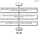
- FIG. 4Apresents a flowchart 400 illustrating a method for facilitating data placement, in accordance with an embodiment of the present application.
- the systemreceives, by a computing device, data to be written to a non-volatile memory, wherein the data is associated with a first logical block address (LBA) (operation 402 ).
- the systemperforms, based on the first logical block address, a search in a mapping table for an entry which indicates a first physical block address associated with a first physical unit (operation 404 ).
- a respective physical unitcomprises a plurality of blocks of data across a plurality of channels of the non-volatile memory.
- the mapping tablemay be maintained and/or searched by a flash translation layer (FTL) module of the computing device. If the entry does not exist in the mapping table (decision 406 ) (i.e., indicating that the data to be written is new data for which an entry has not previously been created), the operation continues at Label A of FIG. 4A .
- FTLflash translation layer
- the systemdetermines a second physical block address in the first physical unit (operation 408 ). For example, the system selects an available block in the same physical unit as the indicated first physical block address returned from the mapping table search.
- the systemwrites the data to the second physical address in the first physical unit (operation 410 ).
- the systemupdates the entry by replacing the first physical block address with the second physical block address (operation 412 ) (e.g., the FTL module updates the mapping table).
- the systemnotifies a host of successfully writing the data to the non-volatile memory (operation 414 ), and the operation continues at Label B of FIG. 4B .
- FIG. 5presents a flowchart illustrating a method 500 for facilitating a garbage collection process, in accordance with an embodiment of the present application.
- the systemidentifies a second physical unit storing data which is to be erased (operation 502 ).
- the systemdetermines one or more current versions of data in the second physical unit by performing a search in the mapping table for one or more physical block addresses in the second physical unit which correspond to a most recent version of data for a given logical block address (operation 504 ).
- the systemcopies out the current versions of data to a third physical unit (operation 506 ).
- the systemerases the data stored in the second physical unit (operation 508 ), and the operation returns.
- FIG. 6illustrates an exemplary computer system that facilitates data placement, in accordance with an embodiment of the present application.
- Computer system 600includes a processor 602 , a controller 604 , a volatile memory 606 , and a storage device 608 .
- Volatile memory 606can include, e.g., random access memory (RAM), that serves as a managed memory, and can be used to store one or more memory pools.
- Storage device 608can include persistent storage which can be managed or accessed via controller 604 .
- computer system 600can be coupled to peripheral input/output (I/O) user devices 610 , e.g., a display device 611 , a keyboard 612 , and a pointing device 614 .
- Storage device 608can store an operating system 616 , a content-processing system 618 , and data 632 .
- I/Operipheral input/output
- Content-processing system 618can include instructions, which when executed by computer system 600 , can cause computer system 600 to perform methods and/or processes described in this disclosure. Specifically, content-processing system 618 can include instructions for receiving and transmitting data packets, including data to be read or written, an input/output (I/O) request (e.g., a read request or a write request), and data associated with an I/O request (communication module 620 ).
- I/Oinput/output
- Content-processing system 618can include instructions for receiving, by a computing device, data to be written to a non-volatile memory, wherein the data is associated with a first logical block address (communication module 620 ).
- Content-processing system 618can include instructions for performing, based on the first logical block address, a search in a mapping table for an entry which indicates a first physical block address associated with a first physical unit (table-searching module 622 ).
- Content-processing system 618can include instructions for writing the data to a second physical block address in the first physical unit (data-writing module 624 ).
- Content-processing system 618can include instructions for updating the entry by replacing the first physical block address with the second physical block address (table-updating module 626 ).
- Data 632can include any data that is required as input or generated as output by the methods and/or processes described in this disclosure. Specifically, data 632 can store at least: data; a request; a read request; a write request; an input/output (I/O) request; data associated with a read request, a write request, or an I/O request; a logical block address (LBA); a physical block address (PBA); an indicator of a physical unit or a channel; an XOR group; a mapping table; an entry in a mapping table; a prior, previous, or expired version of data corresponding to a first LBA; a most recent or current version of data corresponding to the first LBA; an available block; a notification indicating a successful write operation; a new entry; a sequential write; a random write; an indicator of a flash translation layer module; a physical unit storing data which is to be erased; dummy data; an indicator or marking that data is to be recycled; and an indicator or marking that a physical unit
- FIG. 7illustrates an exemplary apparatus that facilitates data placement, in accordance with an embodiment of the present application.
- Apparatus 700can comprise a plurality of units or apparatuses which may communicate with one another via a wired, wireless, quantum light, or electrical communication channel.
- Apparatus 700may be realized using one or more integrated circuits, and may include fewer or more units or apparatuses than those shown in FIG. 7 .
- apparatus 700may be integrated in a computer system, or realized as a separate device(s) which is/are capable of communicating with other computer systems and/or devices.
- apparatus 700can comprise units 702 - 712 which perform functions or operations similar to modules 620 - 630 of computer system 600 of FIG.
- a communication unit 702including: a communication unit 702 ; a table-searching unit 704 ; a data-writing unit 706 ; a table-updating unit 708 ; a garbage-collecting unit 710 ; and a data-processing unit 712 .
- the methods and processes described in the detailed description sectioncan be embodied as code and/or data, which can be stored in a computer-readable storage medium as described above.
- a computer systemreads and executes the code and/or data stored on the computer-readable storage medium, the computer system performs the methods and processes embodied as data structures and code and stored within the computer-readable storage medium.
- the methods and processes described abovecan be included in hardware modules.
- the hardware modulescan include, but are not limited to, application-specific integrated circuit (ASIC) chips, field-programmable gate arrays (FPGAs), and other programmable-logic devices now known or later developed.
- ASICapplication-specific integrated circuit
- FPGAfield-programmable gate arrays
- the hardware modulesWhen the hardware modules are activated, the hardware modules perform the methods and processes included within the hardware modules.
Landscapes
- Engineering & Computer Science (AREA)
- Theoretical Computer Science (AREA)
- Physics & Mathematics (AREA)
- General Engineering & Computer Science (AREA)
- General Physics & Mathematics (AREA)
- Human Computer Interaction (AREA)
- Information Retrieval, Db Structures And Fs Structures Therefor (AREA)
Abstract
Description
This disclosure is generally related to the field of data storage. More specifically, this disclosure is related to a method and system for organizing NAND blocks and placing data to facilitate high-throughput for random writes in a solid state drive.
The proliferation of the Internet and e-commerce continues to create a vast amount of digital content. Various distributed storage systems have been created to access and store such digital content. A storage system can include volatile memory (e.g., dynamic random access memory (DRAM)) and multiple drives (e.g., a solid state drive (SSD) with Not-And (NAND) flash memory) or a hard disk drive (HDD)). Conventional systems can optimize the NAND flash in an SSD for a high-throughput based on a sequential write. However, in a random write, the throughput of a NAND-based SSD can be significantly lower (e.g., one magnitude lower) than the throughput for the sequential write. Furthermore, as the Ethernet bandwidth increases (e.g., growing to greater than 100 Gigabytes (GB)), the random write throughput can become the bottleneck for performance in a storage system.
For example, a server equipped with a 100 GB network interface card (NIC) would require tens of SSDs to match the Ethernet throughput. At the same time, SSDs have evolved to include high-capacity Quad-Level Cell (QLC) NAND, such that the storage capacity of a single server can exceed hundreds of Terabytes (TB). If a single server fails, a large amount of data may become unavailable for a non-negligible amount of recovery time. This can result in an inefficient system, inconsistent behavior, and decreased performance for the overall storage system.
One embodiment provides a system for facilitating data placement. The system receives, by a computing device, data to be written to a non-volatile memory, wherein the data is associated with a first logical block address. The system performs, based on the first logical block address, a search in a mapping table for an entry which indicates a first physical block address associated with a first physical unit. A respective physical unit can comprise a plurality of blocks of data across a plurality of channels of the non-volatile memory. The system writes the data to a second physical block address in the first physical unit. The system updates the entry by replacing the first physical block address with the second physical block address.
In some embodiments, the system determines the second physical block address by selecting an available block in the same first physical unit in which the first physical address resides, wherein a prior version of data corresponding to the first logical block address is stored at the first physical address.
In some embodiments, writing the data to the second physical block address and updating the entry are in response to determining that the entry exists in the mapping table. The system notifies a host of successfully writing the data to the non-volatile memory.
In some embodiments, in response to determining that the entry does not exist in the mapping table: the system writes the data to a third physical block address based on a sequential write; and the system creates, in the mapping table, a new entry which maps the first logical block address to the third physical block address.
In some embodiments, the third physical block address is selected by a flash translation layer module based on a history of channels most recently used to place data in the non-volatile memory.
In some embodiments, the system identifies a second physical unit storing data which is to be erased. The system determines one or more current versions of data in the second physical unit. The system copies out the current versions of data to a third physical unit. The system erases the data stored in the second physical unit.
In some embodiments, determining the one or more current versions of data in the second physical unit comprises performing a search in the mapping table for one or more physical block addresses in the second physical unit which correspond to a most recent version of data for a given logical block address.
In some embodiments, the data to be written is associated with a plurality of logical block address. The system determines that the data associated with the plurality of logical block addresses is successfully written to the first physical unit and one or more other physical units of the non-volatile memory. In response to detecting that a predetermined period of time has passed: the system fills the first physical unit with dummy data; and the system marks the first physical unit as sealed.
In the figures, like reference numerals refer to the same figure elements.
The following description is presented to enable any person skilled in the art to make and use the embodiments, and is provided in the context of a particular application and its requirements. Various modifications to the disclosed embodiments will be readily apparent to those skilled in the art, and the general principles defined herein may be applied to other embodiments and applications without departing from the spirit and scope of the present disclosure. Thus, the embodiments described herein are not limited to the embodiments shown, but are to be accorded the widest scope consistent with the principles and features disclosed herein.
The embodiments described herein solve the bottleneck resulting from the throughput of a random write in a NAND-based SSD by dividing NAND locations into physical units and placing updates to previously stored data in a same physical unit, which allows the SSD to expend fewer resources in performing garbage collection.
As described above, the random write throughput in a NAND-based SSD can become the bottleneck for performance in a storage system. In a random write, certain data associated with certain logical block addresses (LBAs) may be frequently updated (e.g., “hot data”). In general, a flash translation layer (FTL) module can place data in the non-volatile memory based on a timing sequence of when data with a certain LBA is received by the SSD. However, if the placed data corresponds to an update for data which has been previously stored in the non-volatile memory, this may cause a write amplification, as there may be many old or expired versions of the data stored in various physical locations of the non-volatile memory. This can result in the SSD expending a significant amount of resources to perform garbage collection (e.g., because the various expired versions may reside in different areas marked for recycling and copying out at different times, as described below in relation toFIG. 3A ).
Furthermore, the mismatch between the increase of Ethernet bandwidth and the increase of storage capacity can result in a performance bottleneck in the throughput of a random write operation. For example, a server equipped with a 100 GB NIC would require tens of SSDs to match the Ethernet throughput. At the same time, the high storage capacity of, e.g., a QLC NAND, can result in the storage capacity of a single server exceeding hundreds of Terabytes (TB). When a single server fails, a huge amount of data may become unavailable for a non-negligible amount of recovery time. This can result in an inefficient system, inconsistent behavior, and decreased performance for the overall storage system.
Current solutions to address these issues with the random write throughput involve increasing the overprovisioning (OP) of the SSD, which can result in more free blocks to accommodate incoming data and a reduction in triggering of garbage collection. Reducing the triggering of garbage collection can result in an improved write performance in the SSD. However, given a random write, a single data sector can be updated multiple times before the corresponding physical locations are recycled. For example, a small-size data sector can exist in the NAND flash with multiple expired versions in different NAND blocks before those multiple expired versions can be recycled, and over time, any free blocks may become occupied. When a garbage collection process is triggered, various valid data may need to be copied out before a physical location can be recycled. This can lead to an inefficient and limited gain on performance. An example of overprovisioning in the prior art is described below in relation toFIG. 1 .
The embodiments described herein address these challenges and constraints by dividing NAND locations into physical units and placing updates to previously stored data in a same physical unit, which allows the SSD to expend fewer resources in performing garbage collection. A physical unit can include a plurality of data blocks across a plurality of channels of the NAND flash, as described below in relation toFIG. 2 . By placing updates to already-existing data in the same physical unit as prior versions of the data, the system can achieve a reduced triggering of garbage collection, which can lead to an improved performance in the random write throughput, as described below in relation toFIG. 3B . The system can provide more consistent behavior and performance in a distributed storage system, and can result in an improved throughput for a random write operation in a NAND-based SSD, which can also result in improving the overall efficiency and performance of the distributed storage system.
A “storage server” or a “storage node” refers to a computing device which can include multiple storage drives. A distributed storage system can include multiple storage servers. A “storage drive” refers to a device or a drive with a non-volatile memory which can provide persistent storage of data, e.g., a solid state drive (SSD) or a hard disk drive (HDD).
A “physical unit” refers to a unit which includes data blocks across a plurality of NAND channels. A physical unit can include multiple groups of data blocks, and a group of data blocks in a physical unit can form an “Exclusive OR group” or an “XOR group.” An XOR group refers to a group of data blocks which can provide consistency and protection of the stored data in the event that a given data block of the XOR group fails or cannot be accessed (e.g., due to a failure of the NAND die on which the given data block of the XOR group resides).
“Overprovisioning” refers to including additional storage capacity in an SSD, which can result in distributing the total number of writes and erases across a larger number of NAND flash blocks over time. For example, a manufacturer can reserve an additional percentage of the total capacity of a drive for overprovisioning, which can both improve the performance and increase the endurance of the SSD.
Exemplary Environment for Data Placement in the Prior Art
One current solution to reduce the frequency of garbage collection is to increase the amount of OP.FIG. 1B illustrates an exemplary environment for facilitating data placement, including an increased amount of overprovisioning and reduced garbage collection, in accordance with the prior art. InFIG. 1B , a non-volatile memory (NVM)181 (at time t0) includes used blocks121-126 andfree blocks FIG. 1B , the system need not perform garbage collection on the blocks. Instead, because of the additional space available through the increased OP, the system can perform a direct write of the incoming data (141-146) (via a function172), resulting in NVM181 (at time ti).
Thus, the increased OP ofFIG. 1B allows for sufficient free blocks to accommodate an incoming write without triggering garbage collection and recycling blocks, which allows the host data to be written directly to the NAND flash with the full resources of the SSD and without the interference of internal data movement caused by the frequently triggered garbage collection. This in turn can lead to an improved performance in the random write throughput.
However, in the case of a random write operation, challenges can arise because a single data sector may be updated multiple times (resulting in multiple expired versions) prior to erasure of the corresponding physical locations for the multiple expired versions. For example, given a small-sized I/O data (such as 4 Kilobytes), a conventional system may place the small-sized data evenly onto active channels, where a single small-sized data may be updated soon after it is recently written to a non-volatile memory. Thus, a small sector of data can exist in the NAND flash as multiple expired versions stored across different NAND blocks before the garbage collection process can recycle each of the different NAND blocks. As a result, free or OP blocks may gradually become occupied. By increasing the OP, the system may attain an improvement in performance, but the challenge of optimizing efficiency still remains. That is, the system may adjust by increasing to a higher percentage of OP, but the system is still limited in a gain in performance because the many small-size sectors are randomly located in the non-volatile memory and cannot be recycled in a timely manner.
Exemplary Environment for Facilitating Data Placement Using Physical Units Across a Plurality of Channels
The embodiments described herein address the above-described challenges by providing a system which uses a limited amount of OP in an SSD to mitigate the write amplification associated with random write operations, and thus results in an improved random write throughput. The system uses a user-managed flash translation layer to place updates to existing data into a same physical unit which stores prior versions of the data, by spreading each physical unit across multiple NAND flash channels. Each physical unit can also include a plurality of XOR groups for protection and consistency of the data.
During operation, when the system receives an incoming write request, the system can evaluate the logical block address (LBA) of the incoming data to determine whether the write is associated with an update, e.g., by performing a search for a corresponding valid entry in a mapping table managed by a flash translation layer (FTL) module. If a valid entry exists, the system can place the incoming write into the same physical unit as the prior version(s) of data corresponding to the same LBA, as described below in relation toFIGS. 3B and 4A . By placing updates in the same physical unit as prior expired versions, the system can eliminate the chaos of multiple “holes” created across different NAND blocks resulting from random write operations. This allows all expired versions of data corresponding to a single LBA to be erased or recycled as a whole physical unit, which can result in an improved overall storage system.
Exemplary Data Placement and Updating of Prior Versions in the Prior Art Vs. Writing Updated Versions to the Same Physical Unit
In contrast,FIG. 3B illustrates an exemplary data placement and updating of prior versions, in accordance with an embodiment of the present application. InFIG. 3B , the system places multiple versions of data corresponding to the same LBA in the same physical unit. By gathering and storing the expired versions together in this manner, the system can reduce the cost of garbage collection, i.e., reduce the triggering frequency of garbage collection, which can lead to an improved performance in the throughput of a random write operation.
InFIG. 3B ,physical unit 351 includes data corresponding to LBAs “x” and “y,” and also includes both multiple prior expired and the most recent or current versions corresponding to those respective LBAs. For LBA x,physical unit 351 includesversions 1, 2, 3, n, and n+1 as, respectively: LBA_x,V1 362; LBA_x,V2 366; LBA_x,V3 368; LBA_x,Vn 370; and LBA_x, Vn+1372. Similarly, for LBA_y,physical unit 351 includes versions n, n+i, and n+j as, respectively: LBA_y,Vn 364; LBA_y, Vn+i374; and LBA_y, Vn+j376. When the system determines that a garbage collection process is to be performed on physical unit351 (e.g., thatphysical unit 351 is to be recycled), only the most recent version of data corresponding to LBAs x and y need to be copied out (i.e.: LBA_x, Vn+1372; and LBA_y, Vn+j376). This allows the system to subsequently erase and recycle the entirety ofphysical unit 351 by copying out only a minimal number of valid blocks, as opposed to leaving the multiple expired versions of data sitting and spread across multiple NAND blocks waiting to be recycled and taking up crucial space (as described above in relation toFIG. 3A ).
Thus, by reducing the amount of internal write operations based on the reduced triggering of garbage collection, the system can provide an improved throughput for random write operations, which can result in a more efficient overall storage system, as described herein.
Exemplary Method for Facilitating Data Placement
If the entry exists in the mapping table (decision406) (i.e., indicating that the data to be written is an update to data already stored in the non-volatile memory), the system determines a second physical block address in the first physical unit (operation408). For example, the system selects an available block in the same physical unit as the indicated first physical block address returned from the mapping table search. The system writes the data to the second physical address in the first physical unit (operation410). The system updates the entry by replacing the first physical block address with the second physical block address (operation412) (e.g., the FTL module updates the mapping table). The system notifies a host of successfully writing the data to the non-volatile memory (operation414), and the operation continues at Label B ofFIG. 4B .
Exemplary Computer System and Apparatus
Content-processing system 618 can include instructions, which when executed bycomputer system 600, can causecomputer system 600 to perform methods and/or processes described in this disclosure. Specifically, content-processing system 618 can include instructions for receiving and transmitting data packets, including data to be read or written, an input/output (I/O) request (e.g., a read request or a write request), and data associated with an I/O request (communication module620).
Content-processing system 618 can include instructions for receiving, by a computing device, data to be written to a non-volatile memory, wherein the data is associated with a first logical block address (communication module620). Content-processing system 618 can include instructions for performing, based on the first logical block address, a search in a mapping table for an entry which indicates a first physical block address associated with a first physical unit (table-searching module622). Content-processing system 618 can include instructions for writing the data to a second physical block address in the first physical unit (data-writing module624). Content-processing system 618 can include instructions for updating the entry by replacing the first physical block address with the second physical block address (table-updating module626).
Content-processing system 618 can include instructions for determining whether the entry exists in the mapping table (table-searching module622). Content-processing system 618 can include instructions for identifying a second physical unit storing data which is to be erased (garbage-collecting module628). Content-processing system 618 can include instructions for determining one or more current versions of data in the second physical unit table (table-searching module622). Content-processing system 618 can include instructions for copying out the current versions of data to a third physical unit (data-writing module624). Content-processing system 618 can include instructions for erasing the data stored in the second physical unit (data-processing module630).
The data structures and code described in this detailed description are typically stored on a computer-readable storage medium, which may be any device or medium that can store code and/or data for use by a computer system. The computer-readable storage medium includes, but is not limited to, volatile memory, non-volatile memory, magnetic and optical storage devices such as disk drives, magnetic tape, CDs (compact discs), DVDs (digital versatile discs or digital video discs), or other media capable of storing computer-readable media now known or later developed.
The methods and processes described in the detailed description section can be embodied as code and/or data, which can be stored in a computer-readable storage medium as described above. When a computer system reads and executes the code and/or data stored on the computer-readable storage medium, the computer system performs the methods and processes embodied as data structures and code and stored within the computer-readable storage medium.
Furthermore, the methods and processes described above can be included in hardware modules. For example, the hardware modules can include, but are not limited to, application-specific integrated circuit (ASIC) chips, field-programmable gate arrays (FPGAs), and other programmable-logic devices now known or later developed. When the hardware modules are activated, the hardware modules perform the methods and processes included within the hardware modules.
The foregoing embodiments described herein have been presented for purposes of illustration and description only. They are not intended to be exhaustive or to limit the embodiments described herein to the forms disclosed. Accordingly, many modifications and variations will be apparent to practitioners skilled in the art. Additionally, the above disclosure is not intended to limit the embodiments described herein. The scope of the embodiments described herein is defined by the appended claims.
Claims (17)
1. A computer-implemented method for facilitating data placement, the method comprising:
receiving, by a computing device, data to be written to a non-volatile memory which is divided into a plurality of physical units,
wherein a respective physical unit comprises a plurality of Exclusive OR (XOR) groups,
wherein a respective XOR group includes a plurality of blocks of data,
wherein the plurality of blocks of data in the respective XOR group are accessed via a plurality of channels of the non-volatile memory, and
wherein the data is associated with a first logical block address;
performing, based on the first logical block address, a search in a mapping table for an entry which indicates a first physical block address associated with a first physical unit, wherein the first physical block address corresponds to a first block in a first XOR group of the first physical unit, and wherein the first block is accessed via a first channel of the plurality of channels;
determining a second physical block address by selecting an available block in the same first physical unit associated with the first physical block address, wherein the second physical block address corresponds to a second block in the first XOR group of the first physical unit, and wherein a prior version of data corresponding to the first logical block address is stored at the first physical address;
writing the data to the second physical block address corresponding to the second block in the first XOR group of the first physical unit via a second channel of the plurality of channels; and
updating the entry by replacing the first physical block address with the second physical block address.
2. The method ofclaim 1 , wherein writing the data to the second physical block address and updating the entry are in response to determining that the entry exists in the mapping table, and wherein the method further comprises:
notifying a host of successfully writing the data to the non-volatile memory.
3. The method ofclaim 1 , wherein in response to determining that the entry does not exist in the mapping table, the method further comprises:
writing the data to the third physical block address based on a sequential write; and
creating, in the mapping table, a new entry which maps the first logical block address to a third physical block address.
4. The method ofclaim 3 , wherein the third physical block address is selected by a flash translation layer module based on a history of channels most recently used to place data in the non-volatile memory.
5. The method ofclaim 1 , further comprising:
identifying a second physical unit storing data which is to be erased;
determining one or more current versions of data in the second physical unit;
copying out the current versions of data to a third physical unit; and
erasing the data stored in the second physical unit.
6. The method ofclaim 5 , wherein determining the one or more current versions of data in the second physical unit comprises:
performing a search in the mapping table for one or more physical block addresses in the second physical unit which correspond to a most recent version of data for a given logical block address.
7. The method ofclaim 1 , wherein the data to be written is associated with a plurality of logical block address, and wherein the method further comprises:
determining that the data associated with the plurality of logical block addresses is successfully written to the first physical unit and one or more other physical units of the non-volatile memory; and
in response to detecting that a predetermined period of time has passed:
filling the first physical unit with dummy data; and
marking the first physical unit as sealed.
8. A computer system for facilitating data placement, the system comprising:
a processor; and
a memory coupled to the processor and storing instructions, which when executed by the processor cause the processor to perform a method, wherein the computer system is a storage device, the method comprising:
receiving, by the computer system, data to be written to a non-volatile memory which is divided into a plurality of physical units,
wherein a respective physical unit comprises a plurality of Exclusive OR (XOR) groups,
wherein a respective XOR group includes a plurality of blocks of data,
wherein the plurality of blocks of data in the respective XOR group are accessed via a plurality of channels of the non-volatile memory, and
wherein the data is associated with a first logical block address;
performing, based on the first logical block address, a search in a mapping table for an entry which indicates a first physical block address associated with a first physical unit, wherein the first physical block address corresponds to a first block in a first XOR group of the first physical unit, and wherein the first block is accessed via a first channel of the plurality of channels;
determining a second physical block address by selecting an available block in the same first physical unit associated with the first physical block address, wherein the second physical block address corresponds to a second block in the first XOR group of the first physical unit, and wherein a prior version of data corresponding to the first logical block address is stored at the first physical address;
writing the data to the second physical block address corresponding to the second block in the first XOR group of the first physical unit via a second channel of the plurality of channels; and
updating the entry by replacing the first physical block address with the second physical block address.
9. The computer system ofclaim 8 , wherein writing the data to the second physical block address and updating the entry are in response to determining that the entry exists in the mapping table, and wherein the method further comprises:
notifying a host of successfully writing the data to the non-volatile memory.
10. The computer system ofclaim 8 , wherein in response to determining that the entry does not exist in the mapping table, the method further comprises:
writing the data to the third physical block address based on a sequential write; and
creating, in the mapping table, a new entry which maps the first logical block address to a third physical block address.
11. The computer system ofclaim 10 , wherein the third physical block address is selected by a flash translation layer module based on a history of channels most recently used to place data in the non-volatile memory.
12. The computer system ofclaim 8 , wherein the method further comprises:
identifying a second physical unit storing data which is to be erased;
determining one or more current versions of data in the second physical unit;
copying out the current versions of data to a third physical unit; and
erasing the data stored in the second physical unit.
13. The computer system ofclaim 12 , wherein determining the one or more current versions of data in the second physical unit comprises:
performing a search in the mapping table for one or more physical block addresses in the second physical unit which correspond to a most recent version of data for a given logical block address.
14. The computer system ofclaim 8 , wherein the data to be written is associated with a plurality of logical block address, and wherein the method further comprises:
determining that the data associated with the plurality of logical block addresses is successfully written to the first physical unit and one or more other physical units of the non-volatile memory; and
in response to detecting that a predetermined period of time has passed:
filling the first physical unit with dummy data; and
marking the first physical unit as sealed.
15. A non-transitory computer-readable storage medium storing instructions that when executed by a computer cause the computer to perform a method, the method comprising:
receiving, by the computer, data to be written to a non-volatile memory which is divided into a plurality of physical units,
wherein a respective physical unit comprises a plurality of Exclusive OR (XOR) groups,
wherein a respective XOR group includes a plurality of blocks of data,
wherein the plurality of blocks of data in the respective XOR group are accessed via a plurality of channels of the non-volatile memory, and
wherein the data is associated with a first logical block address;
performing, based on the first logical block address, a search in a mapping table for an entry which indicates a first physical block address associated with a first physical unit, wherein the first physical block address corresponds to a first block in a first XOR group of the first physical unit, and wherein the first block is accessed via a first channel of the plurality of channels;
determining a second physical block address by selecting an available block in the same first physical unit associated with the first physical block address, wherein the second physical block address corresponds to a second block in the first XOR group of the first physical unit, and wherein a prior version of data corresponding to the first logical block address is stored at the first physical address;
writing the data to the second physical block address corresponding to the second block in the first XOR group of the first physical unit via a second channel of the plurality of channels; and
updating the entry by replacing the first physical block address with the second physical block address.
16. The storage medium ofclaim 15 , wherein writing the data to the second physical block address and updating the entry are in response to determining that the entry exists in the mapping table, and wherein the method further comprises:
notifying a host of successfully writing the data to the non-volatile memory.
17. The storage medium ofclaim 15 , wherein the method further comprises:
identifying a second physical unit storing data which is to be erased;
determining one or more current versions of data in the second physical unit;
copying out the current versions of data to a third physical unit; and
erasing the data stored in the second physical unit.
Priority Applications (2)
| Application Number | Priority Date | Filing Date | Title |
|---|---|---|---|
| US16/589,802US11126561B2 (en) | 2019-10-01 | 2019-10-01 | Method and system for organizing NAND blocks and placing data to facilitate high-throughput for random writes in a solid state drive |
| CN202011022830.6ACN112596667B (en) | 2019-10-01 | 2020-09-25 | High throughput method and system for organizing NAND blocks and placing data in a solid state drive to facilitate random writing |
Applications Claiming Priority (1)
| Application Number | Priority Date | Filing Date | Title |
|---|---|---|---|
| US16/589,802US11126561B2 (en) | 2019-10-01 | 2019-10-01 | Method and system for organizing NAND blocks and placing data to facilitate high-throughput for random writes in a solid state drive |
Publications (2)
| Publication Number | Publication Date |
|---|---|
| US20210097003A1 US20210097003A1 (en) | 2021-04-01 |
| US11126561B2true US11126561B2 (en) | 2021-09-21 |
Family
ID=75163407
Family Applications (1)
| Application Number | Title | Priority Date | Filing Date |
|---|---|---|---|
| US16/589,802Active2039-12-13US11126561B2 (en) | 2019-10-01 | 2019-10-01 | Method and system for organizing NAND blocks and placing data to facilitate high-throughput for random writes in a solid state drive |
Country Status (2)
| Country | Link |
|---|---|
| US (1) | US11126561B2 (en) |
| CN (1) | CN112596667B (en) |
Cited By (7)
| Publication number | Priority date | Publication date | Assignee | Title |
|---|---|---|---|---|
| US11507499B2 (en) | 2020-05-19 | 2022-11-22 | Alibaba Group Holding Limited | System and method for facilitating mitigation of read/write amplification in data compression |
| US11556277B2 (en)* | 2020-05-19 | 2023-01-17 | Alibaba Group Holding Limited | System and method for facilitating improved performance in ordering key-value storage with input/output stack simplification |
| US11617282B2 (en) | 2019-10-01 | 2023-03-28 | Alibaba Group Holding Limited | System and method for reshaping power budget of cabinet to facilitate improved deployment density of servers |
| US11726699B2 (en) | 2021-03-30 | 2023-08-15 | Alibaba Singapore Holding Private Limited | Method and system for facilitating multi-stream sequential read performance improvement with reduced read amplification |
| US11734115B2 (en) | 2020-12-28 | 2023-08-22 | Alibaba Group Holding Limited | Method and system for facilitating write latency reduction in a queue depth of one scenario |
| US11768709B2 (en) | 2019-01-02 | 2023-09-26 | Alibaba Group Holding Limited | System and method for offloading computation to storage nodes in distributed system |
| US11816043B2 (en) | 2018-06-25 | 2023-11-14 | Alibaba Group Holding Limited | System and method for managing resources of a storage device and quantifying the cost of I/O requests |
Families Citing this family (2)
| Publication number | Priority date | Publication date | Assignee | Title |
|---|---|---|---|---|
| CN114415963B (en)* | 2021-12-03 | 2023-09-19 | 武汉深之度科技有限公司 | Hard disk data cleaning method and device and computing equipment |
| EP4346158A1 (en)* | 2022-09-30 | 2024-04-03 | IHP GmbH - Innovations for High Performance Microelectronics / Leibniz-Institut für innovative Mikroelektronik | Cryptographic hardware accelerator with dummy-addressing of blocks for protection against physical attacks |
Citations (312)
| Publication number | Priority date | Publication date | Assignee | Title |
|---|---|---|---|---|
| US3893071A (en) | 1974-08-19 | 1975-07-01 | Ibm | Multi level error correction system for high density memory |
| US4562494A (en) | 1983-04-07 | 1985-12-31 | Verbatim Corporation | Disk drive alignment analyzer |
| US4718067A (en) | 1984-08-02 | 1988-01-05 | U.S. Philips Corporation | Device for correcting and concealing errors in a data stream, and video and/or audio reproduction apparatus comprising such a device |
| US4775932A (en) | 1984-07-31 | 1988-10-04 | Texas Instruments Incorporated | Computer memory system with parallel garbage collection independent from an associated user processor |
| US4858040A (en) | 1987-08-25 | 1989-08-15 | Ampex Corporation | Bimorph actuator for a disk drive |
| WO1994018634A1 (en) | 1993-02-01 | 1994-08-18 | Lsc, Inc. | Archiving file system for data servers in a distributed network environment |
| US5394382A (en) | 1993-02-11 | 1995-02-28 | International Business Machines Corporation | Method for the organization of data on a CD-ROM |
| US5602693A (en) | 1994-12-14 | 1997-02-11 | Micropolis (S) Pte Ltd. | Method and apparatus for sensing position in a disk drive |
| US5732093A (en) | 1996-02-08 | 1998-03-24 | United Microelectronics Corporation | Error correction method and apparatus on optical disc system |
| US5802551A (en) | 1993-10-01 | 1998-09-01 | Fujitsu Limited | Method and apparatus for controlling the writing and erasing of information in a memory device |
| US5930167A (en) | 1997-07-30 | 1999-07-27 | Sandisk Corporation | Multi-state non-volatile flash memory capable of being its own two state write cache |
| US6098185A (en) | 1997-10-31 | 2000-08-01 | Stmicroelectronics, N.V. | Header-formatted defective sector management system |
| US6148377A (en) | 1996-11-22 | 2000-11-14 | Mangosoft Corporation | Shared memory computer networks |
| US6226650B1 (en) | 1998-09-17 | 2001-05-01 | Synchrologic, Inc. | Database synchronization and organization system and method |
| US6243795B1 (en) | 1998-08-04 | 2001-06-05 | The Board Of Governors For Higher Education, State Of Rhode Island And Providence Plantations | Redundant, asymmetrically parallel disk cache for a data storage system |
| US20010032324A1 (en) | 1998-05-12 | 2001-10-18 | Slaughter Gregory L. | Highly available cluster message passing facility |
| US20020010783A1 (en) | 1999-12-06 | 2002-01-24 | Leonard Primak | System and method for enhancing operation of a web server cluster |
| US20020039260A1 (en) | 1995-11-28 | 2002-04-04 | Kilmer Dan L. | Twin coil positioner |
| US20020073358A1 (en) | 2000-12-07 | 2002-06-13 | Atkinson Lee. W. | Method for redundant suspend to RAM |
| US20020095403A1 (en) | 1998-11-24 | 2002-07-18 | Sashikanth Chandrasekaran | Methods to perform disk writes in a distributed shared disk system needing consistency across failures |
| US6457104B1 (en) | 2000-03-20 | 2002-09-24 | International Business Machines Corporation | System and method for recycling stale memory content in compressed memory systems |
| US20020161890A1 (en) | 2000-12-22 | 2002-10-31 | Kailai Chen | System and method for intelligently distributing content over a communicatons network |
| JP2003022209A (en) | 2001-07-05 | 2003-01-24 | Nri & Ncc Co Ltd | Distributed server system |
| US20030074319A1 (en) | 2001-10-11 | 2003-04-17 | International Business Machines Corporation | Method, system, and program for securely providing keys to encode and decode data in a storage cartridge |
| US20030145274A1 (en) | 2002-01-23 | 2003-07-31 | Samsung Electronics Co., Ltd. | Decoding method and apparatus therefor |
| US20030163633A1 (en) | 2002-02-27 | 2003-08-28 | Aasheim Jered Donald | System and method for achieving uniform wear levels in a flash memory device |
| US20030163594A1 (en) | 2002-02-27 | 2003-08-28 | Aasheim Jered Donald | Open-architecture file system |
| US20030217080A1 (en) | 2002-05-20 | 2003-11-20 | Ken White | System and method for intelligent write management of disk pages in cache checkpoint operations |
| US6658478B1 (en) | 2000-08-04 | 2003-12-02 | 3Pardata, Inc. | Data storage system |
| US20040010545A1 (en) | 2002-06-11 | 2004-01-15 | Pandya Ashish A. | Data processing system using internet protocols and RDMA |
| US20040066741A1 (en) | 2002-09-23 | 2004-04-08 | Darpan Dinker | System and method for performing a cluster topology self-healing process in a distributed data system cluster |
| US20040103238A1 (en) | 2002-11-26 | 2004-05-27 | M-Systems Flash Disk Pioneers Ltd. | Appliance, including a flash memory, that is robust under power failure |
| US20040143718A1 (en) | 2003-01-22 | 2004-07-22 | Tianlong Chen | Distributed memory computing environment and implementation thereof |
| US6795894B1 (en) | 2000-08-08 | 2004-09-21 | Hewlett-Packard Development Company, L.P. | Fast disk cache writing system |
| US20040255171A1 (en) | 2003-06-13 | 2004-12-16 | Zimmer Vincent J. | Power management for clustered computing platforms |
| US20040268278A1 (en) | 2003-05-07 | 2004-12-30 | Hoberman Barry Alan | Managing power on integrated circuits using power islands |
| US20050038954A1 (en) | 2003-06-04 | 2005-02-17 | Quantum Corporation | Storage drive having universal format across media types |
| US20050097126A1 (en) | 2000-08-24 | 2005-05-05 | Microsoft Corporation | Partial migration of an object to another storage location in a computer system |
| US20050149827A1 (en) | 2002-01-24 | 2005-07-07 | Nicolaas Lambert | Data storage apparatus and method for handling a data storage apparatus |
| US20050177755A1 (en) | 2000-09-27 | 2005-08-11 | Amphus, Inc. | Multi-server and multi-CPU power management system and method |
| US20050177672A1 (en) | 2004-02-10 | 2005-08-11 | Sun Microsystems, Inc. | Storage system structure for storing relational cache metadata |
| US20050174670A1 (en) | 2004-02-10 | 2005-08-11 | Hitachi Global Storage Technologies Netherlands Bv | Adaptive data format method integrating spare sectors |
| US20050195635A1 (en) | 2004-03-08 | 2005-09-08 | Conley Kevin M. | Flash controller cache architecture |
| US20050235067A1 (en) | 2004-04-20 | 2005-10-20 | Intel Corporation | Write combining protocol between processors and chipsets |
| US20050235171A1 (en) | 2003-09-02 | 2005-10-20 | Kabushiki Kaisha Toshiba | Electronic device with serial ATA interface and power saving method for serial ATA buses |
| US20060031709A1 (en) | 2004-08-09 | 2006-02-09 | Yuri Hiraiwa | Failure monitoring for storage systems constituting multiple stages |
| US20060156012A1 (en) | 2005-01-07 | 2006-07-13 | Beeson Curtis L | Facilitating digital signature based on ephemeral private key |
| US20070033323A1 (en) | 2005-08-03 | 2007-02-08 | Gorobets Sergey A | Interfacing systems operating through a logical address space and on a direct data file basis |
| US20070061502A1 (en) | 2005-09-09 | 2007-03-15 | M-Systems Flash Disk Pioneers Ltd. | Flash memory storage system and method |
| US20070101096A1 (en) | 2005-10-27 | 2007-05-03 | Sandisk Corporation | Non-volatile memory with adaptive handling of data writes |
| US20070283081A1 (en) | 2006-06-06 | 2007-12-06 | Msystem Ltd. | Cache control in a non-volatile memory device |
| US20070285980A1 (en) | 2006-05-10 | 2007-12-13 | Takahiro Shimizu | Semiconductor memory device |
| US20080034154A1 (en) | 1999-08-04 | 2008-02-07 | Super Talent Electronics Inc. | Multi-Channel Flash Module with Plane-Interleaved Sequential ECC Writes and Background Recycling to Restricted-Write Flash Chips |
| US20080065805A1 (en) | 2006-09-11 | 2008-03-13 | Cameo Communications, Inc. | PCI-Express multimode expansion card and communication device having the same |
| US7351072B2 (en) | 2005-07-08 | 2008-04-01 | Qimonda Ag | Memory module, memory extension memory module, memory module system, and method for manufacturing a memory module |
| US20080082731A1 (en) | 2006-09-28 | 2008-04-03 | Vijay Karamcheti | Main memory in a system with a memory controller configured to control access to non-volatile memory, and related technologies |
| US20080112238A1 (en) | 2006-10-25 | 2008-05-15 | Seon-Taek Kim | Hybrid flash memory device and method for assigning reserved blocks thereof |
| US20080301532A1 (en) | 2006-09-25 | 2008-12-04 | Kabushiki Kaisha Toshiba | Non-volatile semiconductor memory device |
| US20090006667A1 (en) | 2007-06-29 | 2009-01-01 | Sandisk Corporation, A Delaware Corporation | Secure digital host sector application flag compression |
| US20090089544A1 (en) | 2007-10-01 | 2009-04-02 | Accenture Global Services Gmbh | Infrastructure for parallel programming of clusters of machines |
| US20090113219A1 (en) | 2007-10-30 | 2009-04-30 | Sandisk Il Ltd. | Optimized hierarchical integrity protection for stored data |
| US20090183052A1 (en) | 2007-08-31 | 2009-07-16 | Shinichi Kanno | Semiconductor memory device and method of controlling the same |
| US7565454B2 (en) | 2003-07-18 | 2009-07-21 | Microsoft Corporation | State migration in multiple NIC RDMA enabled devices |
| US7599139B1 (en) | 2007-06-22 | 2009-10-06 | Western Digital Technologies, Inc. | Disk drive having a high performance access mode and a lower performance archive mode |
| US20090282275A1 (en) | 2006-06-27 | 2009-11-12 | Koninklijke Philips Electronics N.V. | Device and a method for managing power consumption of a plurality of data processing units |
| US20090287956A1 (en) | 2008-05-16 | 2009-11-19 | David Flynn | Apparatus, system, and method for detecting and replacing failed data storage |
| US20090307249A1 (en) | 2006-05-31 | 2009-12-10 | Storwize Ltd. | Method and system for transformation of logical data objects for storage |
| US20090310412A1 (en) | 2008-06-17 | 2009-12-17 | Jun-Ho Jang | Methods of data management in non-volatile memory devices and related non-volatile memory systems |
| US20100031000A1 (en) | 2007-12-06 | 2010-02-04 | David Flynn | Apparatus, system, and method for validating that a correct data segment is read from a data storage device |
| US20100169470A1 (en) | 2008-12-25 | 2010-07-01 | Hitachi, Ltd. | System and method for operational management of computer system |
| US20100217952A1 (en) | 2009-02-26 | 2010-08-26 | Iyer Rahul N | Remapping of Data Addresses for a Large Capacity Victim Cache |
| US20100229224A1 (en) | 2009-02-10 | 2010-09-09 | Uniloc Usa, Inc. | Web Content Access Using a Client Device Identifier |
| US20100241848A1 (en) | 2009-02-27 | 2010-09-23 | Certicom Corp. | System and method for securely communicating with electronic meters |
| US20100321999A1 (en) | 2009-06-23 | 2010-12-23 | Samsung Electronics Co., Ltd. | Nonvolatile memory device and related programming method |
| US20100325367A1 (en) | 2009-06-19 | 2010-12-23 | International Business Machines Corporation | Write-Back Coherency Data Cache for Resolving Read/Write Conflicts |
| US20100332922A1 (en) | 2009-06-30 | 2010-12-30 | Mediatek Inc. | Method for managing device and solid state disk drive utilizing the same |
| US20110031546A1 (en) | 2009-08-06 | 2011-02-10 | Kabushiki Kaisha Toshiba | Method for manufacturing semiconductor device and apparatus for manufacturing same |
| US20110055471A1 (en) | 2009-08-28 | 2011-03-03 | Jonathan Thatcher | Apparatus, system, and method for improved data deduplication |
| US20110055458A1 (en) | 2009-09-03 | 2011-03-03 | 248 Solid State, Inc. | Page based management of flash storage |
| US20110072204A1 (en) | 2008-07-03 | 2011-03-24 | Jichuan Chang | Memory server |
| US20110099418A1 (en) | 2009-10-28 | 2011-04-28 | Jian Chen | Non-Volatile Memory And Method With Post-Write Read And Adaptive Re-Write To Manage Errors |
| US7953899B1 (en) | 2002-08-21 | 2011-05-31 | 3Par Inc. | Universal diagnostic hardware space access system for firmware |
| US7958433B1 (en) | 2006-11-30 | 2011-06-07 | Marvell International Ltd. | Methods and systems for storing data in memory using zoning |
| US20110153903A1 (en) | 2009-12-21 | 2011-06-23 | Sanmina-Sci Corporation | Method and apparatus for supporting storage modules in standard memory and/or hybrid memory bus architectures |
| US20110161784A1 (en) | 2009-12-30 | 2011-06-30 | Selinger Robert D | Method and Controller for Performing a Copy-Back Operation |
| US20110191525A1 (en) | 2010-02-04 | 2011-08-04 | Phison Electronics Corp. | Flash memory storage device, controller thereof, and data programming method thereof |
| US20110218969A1 (en) | 2010-03-08 | 2011-09-08 | International Business Machines Corporation | Approach for optimizing restores of deduplicated data |
| JP2011175422A (en) | 2010-02-24 | 2011-09-08 | Fujitsu Ltd | Determination program, method and device |
| US20110231598A1 (en) | 2010-03-19 | 2011-09-22 | Kabushiki Kaisha Toshiba | Memory system and controller |
| US20110239083A1 (en) | 2010-03-24 | 2011-09-29 | Kabushiki Kaisha Toshiba | Semiconductor memory device |
| US20110252188A1 (en) | 2010-04-07 | 2011-10-13 | Hanan Weingarten | System and method for storing information in a multi-level cell memory |
| US20110258514A1 (en) | 2010-01-28 | 2011-10-20 | Sandisk Il Ltd. | Overlapping error correction operations |
| US20110292538A1 (en) | 2010-05-31 | 2011-12-01 | Kabushiki Kaisha Toshiba | Recording medium controller and method thereof |
| US20110302353A1 (en) | 2008-12-30 | 2011-12-08 | Emanuele Confalonieri | Non-volatile memory with extended operating temperature range |
| US20110299317A1 (en) | 2006-11-29 | 2011-12-08 | Shaeffer Ian P | Integrated circuit heating to effect in-situ annealing |
| US8085569B2 (en) | 2006-12-28 | 2011-12-27 | Hynix Semiconductor Inc. | Semiconductor memory device, and multi-chip package and method of operating the same |
| US20120039117A1 (en) | 2010-08-16 | 2012-02-16 | Gary Edward Webb | Destruction of data stored in phase change memory |
| US8144512B2 (en) | 2009-12-18 | 2012-03-27 | Sandisk Technologies Inc. | Data transfer flows for on-chip folding |
| US20120084523A1 (en) | 2010-09-30 | 2012-04-05 | Littlefield Duncan A | Data recovery operations, such as recovery from modified network data management protocol data |
| US20120089774A1 (en) | 2010-10-12 | 2012-04-12 | International Business Machines Corporation | Method and system for mitigating adjacent track erasure in hard disk drives |
| US20120096330A1 (en) | 2010-10-19 | 2012-04-19 | Mosaid Technologies Incorporated | Error detection and correction codes for channels and memories with incomplete error characteristics |
| US8166233B2 (en) | 2009-07-24 | 2012-04-24 | Lsi Corporation | Garbage collection for solid state disks |
| US20120117399A1 (en) | 2010-11-04 | 2012-05-10 | International Business Machines Corporation | Saving power by managing the state of inactive computing devices |
| US20120147021A1 (en) | 2010-12-13 | 2012-06-14 | Advanced Micro Devices, Inc. | Graphics compute process scheduling |
| US20120159099A1 (en) | 2010-12-17 | 2012-06-21 | Jack William Lindamood | Distributed Storage System |
| US20120159289A1 (en) | 2010-12-20 | 2012-06-21 | Piccirillo Gary J | Data signatures to determine sucessful completion of memory backup |
| US20120173792A1 (en) | 2010-12-30 | 2012-07-05 | Lassa Paul A | Controller and Method for Performing Background Operations |
| US20120203958A1 (en) | 2011-02-08 | 2012-08-09 | SMART Storage Systems, Inc. | Storage control system with change logging mechanism and method of operation thereof |
| US20120210095A1 (en) | 2011-02-11 | 2012-08-16 | Fusion-Io, Inc. | Apparatus, system, and method for application direct virtual memory management |
| US8260924B2 (en) | 2006-05-03 | 2012-09-04 | Bluetie, Inc. | User load balancing systems and methods thereof |
| US20120233523A1 (en) | 2011-03-10 | 2012-09-13 | Icform, Inc | Programmable Data Storage Management |
| US20120246392A1 (en) | 2011-03-23 | 2012-09-27 | Samsung Electronics Co., Ltd. | Storage device with buffer memory including non-volatile ram and volatile ram |
| US8281061B2 (en) | 2008-03-31 | 2012-10-02 | Micron Technology, Inc. | Data conditioning to improve flash memory reliability |
| US20120278579A1 (en) | 2011-04-29 | 2012-11-01 | Seagate Technology Llc | Self-Initiated Secure Erasure Responsive to an Unauthorized Power Down Event |
| US20120284587A1 (en) | 2008-06-18 | 2012-11-08 | Super Talent Electronics, Inc. | Super-Endurance Solid-State Drive with Endurance Translation Layer (ETL) and Diversion of Temp Files for Reduced Flash Wear |
| US20120331207A1 (en) | 2011-06-24 | 2012-12-27 | Lassa Paul A | Controller, Storage Device, and Method for Power Throttling Memory Operations |
| US20130013880A1 (en) | 2011-07-08 | 2013-01-10 | Hitachi Computer Peripherals Co., Ltd. | Storage system and its data processing method |
| US20130024605A1 (en) | 2011-07-22 | 2013-01-24 | Sandisk Technologies Inc. | Systems and methods of storing data |
| US20130054822A1 (en) | 2011-08-30 | 2013-02-28 | Rajiv P. Mordani | Failover Data Replication with Colocation of Session State Data |
| US20130061029A1 (en) | 2011-09-02 | 2013-03-07 | Lsi Corporation | Method and apparatus for consolidating boot drives and improving reliability/availability/serviceability in high density server environments |
| US20130073798A1 (en) | 2011-09-20 | 2013-03-21 | Samsung Electronics Co., Ltd. | Flash memory device and data management method |
| US20130080391A1 (en) | 2011-09-23 | 2013-03-28 | International Business Machines Corporation | Block level backup and restore |
| US8452819B1 (en) | 2011-03-22 | 2013-05-28 | Amazon Technologies, Inc. | Methods and apparatus for optimizing resource utilization in distributed storage systems |
| US20130145089A1 (en) | 2010-05-28 | 2013-06-06 | International Business Machines Corporation | Cache memory management in a flash cache architecture |
| US20130145085A1 (en) | 2008-06-18 | 2013-06-06 | Super Talent Technology Corp. | Virtual Memory Device (VMD) Application/Driver with Dual-Level Interception for Data-Type Splitting, Meta-Page Grouping, and Diversion of Temp Files to Ramdisks for Enhanced Flash Endurance |
| US20130151759A1 (en) | 2011-12-08 | 2013-06-13 | Samsung Electronics Co., Ltd. | Storage device and operating method eliminating duplicate data storage |
| US20130159723A1 (en) | 2010-09-23 | 2013-06-20 | Marc Brandt | Methods, apparatus and systems for monitoring locations of data within a network service |
| US20130159251A1 (en) | 2009-06-19 | 2013-06-20 | Rich Skrenta | Dedicating Disks to Reading or Writing |
| US20130166820A1 (en) | 2011-12-22 | 2013-06-27 | Fusion-Io, Inc. | Methods and appratuses for atomic storage operations |
| US20130173845A1 (en) | 2011-12-29 | 2013-07-04 | Ameen Aslam | Command Aware Partial Page Programming |
| US20130191601A1 (en) | 2012-01-24 | 2013-07-25 | Fusion-Io, Inc. | Apparatus, system, and method for managing a cache |
| US20130219131A1 (en) | 2012-02-20 | 2013-08-22 | Nimrod Alexandron | Low access time indirect memory accesses |
| US8527544B1 (en) | 2011-08-11 | 2013-09-03 | Pure Storage Inc. | Garbage collection in a storage system |
| US20130238955A1 (en) | 2012-03-09 | 2013-09-12 | Sandisk Technologies Inc. | System and method to decode data subject to a disturb condition |
| US20130318283A1 (en) | 2012-05-22 | 2013-11-28 | Netapp, Inc. | Specializing i/0 access patterns for flash storage |
| US20130318395A1 (en) | 2012-03-28 | 2013-11-28 | Pranav Kalavade | Reconstructing codewords using a side channel |
| US20140006688A1 (en) | 2012-07-02 | 2014-01-02 | Super Talent Technology, Corp. | Endurance and Retention Flash Controller with Programmable Binary-Levels-Per-Cell Bits Identifying Pages or Blocks as having Triple, Multi, or Single-Level Flash-Memory Cells |
| US20140019650A1 (en) | 2012-07-10 | 2014-01-16 | Zhi Bin Li | Multi-Write Bit-Fill FIFO |
| US20140025638A1 (en) | 2011-03-22 | 2014-01-23 | Zte Corporation | Method, system and serving node for data backup and restoration |
| US20140082273A1 (en) | 2012-09-20 | 2014-03-20 | XtremlO Ltd. | Content addressable storage in legacy systems |
| US20140095827A1 (en) | 2011-05-24 | 2014-04-03 | Agency For Science, Technology And Research | Memory storage device, and a related zone-based block management and mapping method |
| US20140108414A1 (en) | 2012-10-12 | 2014-04-17 | Architecture Technology Corporation | Scalable distributed processing of rdf data |
| US8751763B1 (en) | 2013-03-13 | 2014-06-10 | Nimbus Data Systems, Inc. | Low-overhead deduplication within a block-based data storage |
| US20140181532A1 (en) | 2010-12-31 | 2014-06-26 | International Business Machines Corporation | Encrypted flash-based data storage system with confidentiality mode |
| US20140195564A1 (en) | 2010-12-13 | 2014-07-10 | Fusion-Io, Inc. | Persistent data structures |
| US20140233950A1 (en) | 2013-02-15 | 2014-08-21 | Futurewei Technologies, Inc. | Downstream Burst Transmission In Passive Optical Networks |
| US8819367B1 (en)* | 2011-12-19 | 2014-08-26 | Western Digital Technologies, Inc. | Accelerated translation power recovery |
| US8825937B2 (en) | 2011-02-25 | 2014-09-02 | Fusion-Io, Inc. | Writing cached data forward on read |
| US20140250259A1 (en) | 2013-03-01 | 2014-09-04 | Silicon Motion, Inc. | Data storage device and flash memory control method |
| US20140279927A1 (en) | 2013-03-15 | 2014-09-18 | International Business Machines Corporation | Scalable graph modeling of metadata for deduplicated storage systems |
| US20140304452A1 (en) | 2013-04-03 | 2014-10-09 | Violin Memory Inc. | Method for increasing storage media performance |
| US20140310574A1 (en) | 2012-12-28 | 2014-10-16 | Super Talent Technology, Corp. | Green eMMC Device (GeD) Controller with DRAM Data Persistence, Data-Type Splitting, Meta-Page Grouping, and Diversion of Temp Files for Enhanced Flash Endurance |
| US8868825B1 (en) | 2014-07-02 | 2014-10-21 | Pure Storage, Inc. | Nonrepeating identifiers in an address space of a non-volatile solid-state storage |
| US8904061B1 (en) | 2011-12-30 | 2014-12-02 | Emc Corporation | Managing storage operations in a server cache |
| US20140359229A1 (en) | 2013-05-31 | 2014-12-04 | Vmware, Inc. | Lightweight Remote Replication of a Local Write-Back Cache |
| US20140365707A1 (en) | 2010-12-13 | 2014-12-11 | Fusion-Io, Inc. | Memory device with volatile and non-volatile media |
| US20150019798A1 (en) | 2013-07-15 | 2015-01-15 | CNEXLABS, Inc. | Method and Apparatus for Providing Dual Memory Access to Non-Volatile Memory |
| US8949208B1 (en) | 2011-09-30 | 2015-02-03 | Emc Corporation | System and method for bulk data movement between storage tiers |
| US20150082317A1 (en) | 2013-09-19 | 2015-03-19 | Liang You | Techniques for distributed processing task portion assignment |
| US20150106559A1 (en) | 2013-03-15 | 2015-04-16 | Samsung Electronics Co., Ltd. | Nonvolatile storage device and operating system (os) image program method thereof |
| US20150106556A1 (en) | 2008-06-18 | 2015-04-16 | Super Talent Electronics, Inc. | Endurance Translation Layer (ETL) and Diversion of Temp Files for Reduced Flash Wear of a Super-Endurance Solid-State Drive |
| US9015561B1 (en) | 2014-06-11 | 2015-04-21 | Sandisk Technologies Inc. | Adaptive redundancy in three dimensional memory |
| US20150121031A1 (en) | 2013-10-25 | 2015-04-30 | Seagate Technology Llc | Adaptive guard band for improved data storage capacity |
| US20150142752A1 (en) | 2013-11-15 | 2015-05-21 | International Business Machines Corporation | Priority based reliability mechanism for archived data |
| US9043545B2 (en) | 2012-01-06 | 2015-05-26 | Netapp, Inc. | Distributing capacity slices across storage system nodes |
| US20150199234A1 (en) | 2014-01-13 | 2015-07-16 | Samsung Electronics Co., Ltd. | Memory device, memory system, and method of operating memory device |
| US9088300B1 (en) | 2011-12-15 | 2015-07-21 | Marvell International Ltd. | Cyclic redundancy check for out-of-order codewords |
| US9092223B1 (en) | 2012-05-31 | 2015-07-28 | Google Inc. | Systems and methods to save power in data-center networks |
| US20150227316A1 (en) | 2014-02-07 | 2015-08-13 | Coho Data, Inc. | Methods, systems and devices relating to data storage interfaces for managing data address spaces in data storage devices |
| US20150234845A1 (en) | 2014-02-17 | 2015-08-20 | Netapp, Inc. | Subpartitioning of a namespace region |
| US9129628B1 (en) | 2014-10-23 | 2015-09-08 | Western Digital Technologies, Inc. | Data management for data storage device with different track density regions |
| US9141176B1 (en) | 2013-07-29 | 2015-09-22 | Western Digital Technologies, Inc. | Power management for data storage device |
| US20150269964A1 (en) | 2014-03-21 | 2015-09-24 | Western Digital Technologies, Inc. | Data management for a data storage device using a last resort zone |
| US20150277937A1 (en) | 2014-03-26 | 2015-10-01 | Robert C. Swanson | Boot image discovery and delivery |
| US20150294684A1 (en) | 2014-04-10 | 2015-10-15 | Seagate Technology Llc | Band rewrite optimization |
| US20150304108A1 (en) | 2010-09-15 | 2015-10-22 | Seagate Technology Llc | Encryption Key Destruction For Secure Data Erasure |
| US20150301964A1 (en) | 2014-02-18 | 2015-10-22 | Alistair Mark Brinicombe | Methods and systems of multi-memory, control and data plane architecture |
| US20150347025A1 (en) | 2014-05-27 | 2015-12-03 | Kabushiki Kaisha Toshiba | Host-controlled garbage collection |
| US9208817B1 (en) | 2015-03-10 | 2015-12-08 | Alibaba Group Holding Limited | System and method for determination and reallocation of pending sectors caused by media fatigue |
| US9213627B2 (en)* | 2005-12-21 | 2015-12-15 | Nxp B.V. | Non-volatile memory with block erasable locations |
| US20150363271A1 (en) | 2014-06-16 | 2015-12-17 | International Business Machines Corporation | Restoring data in a hierarchical storage management system |
| US20150363328A1 (en) | 2013-01-18 | 2015-12-17 | Cisco Technology, Inc. | Methods and apparatus for data processing |
| US20150372597A1 (en) | 2014-06-19 | 2015-12-24 | Shiguo Luo | Methods and systems for improving light load efficiency for power stages of multi-phase voltage regulator circuits |
| US20160014039A1 (en) | 2014-07-11 | 2016-01-14 | Vmware, Inc. | Methods and apparatus to provision a workload in a virtual server rack deployment |
| US20160026575A1 (en) | 2014-07-22 | 2016-01-28 | Lsi Corporation | Selective mirroring in caches for logical volumes |
| US20160041760A1 (en) | 2014-08-08 | 2016-02-11 | International Business Machines Corporation | Multi-Level Cell Flash Memory Control Mechanisms |
| US20160048341A1 (en) | 2012-06-29 | 2016-02-18 | International Business Machines Corporation | Optimized data placement for individual file accesses on deduplication-enabled sequential storage systems |
| US9280472B1 (en) | 2013-03-13 | 2016-03-08 | Western Digital Technologies, Inc. | Caching data in a high performance zone of a data storage system |
| US20160077968A1 (en) | 2014-09-16 | 2016-03-17 | Sandisk Technologies Inc. | System and method for configuring and controlling non-volatile cache |
| US20160077749A1 (en) | 2014-09-16 | 2016-03-17 | Sandisk Technologies Inc. | Adaptive Block Allocation in Nonvolatile Memory |
| US20160098344A1 (en) | 2014-10-03 | 2016-04-07 | Sandisk Technologies Inc. | Hardware automation for memory management |
| US20160098350A1 (en) | 2014-10-06 | 2016-04-07 | Sk Hynix Memory Solutions Inc. | Sizing a cache while taking into account a total bytes written requirement |
| US9311939B1 (en) | 2014-12-23 | 2016-04-12 | Western Digital Technologies, Inc. | Write-through media caching |
| US20160103631A1 (en) | 2014-10-13 | 2016-04-14 | Silicon Motion, Inc. | Non-volatile memory devices and control methods therefor |
| US20160110254A1 (en) | 2014-10-15 | 2016-04-21 | Empire Technology Development Llc | Partial Cloud Data Storage |
| US9336340B1 (en) | 2012-03-30 | 2016-05-10 | Emc Corporation | Evaluating management operations |
| US20160155750A1 (en) | 2014-11-28 | 2016-06-02 | Kabushiki Kaisha Toshiba | Semiconductor memory device and method for manufacturing the same |
| US20160154601A1 (en) | 2014-11-28 | 2016-06-02 | International Business Machines Corporation | Disk management in distributed storage system |
| US20160162187A1 (en) | 2013-04-17 | 2016-06-09 | The-Aio Co., Ltd. | Storage System And Method For Processing Writing Data Of Storage System |
| US20160179399A1 (en) | 2014-12-23 | 2016-06-23 | Sandisk Technologies Inc. | System and Method for Selecting Blocks for Garbage Collection Based on Block Health |
| US20160188890A1 (en) | 2014-12-26 | 2016-06-30 | Intel Corporation | Security mode data protection |
| US20160188223A1 (en) | 2014-12-30 | 2016-06-30 | International Business Machines Corporation | Promoting consistent response times in a data storage system having multiple data retrieval mechanisms |
| US20160203000A1 (en) | 2015-01-09 | 2016-07-14 | Avago Technologies General Ip (Singapore) Pte. Ltd | Operating system software install and boot up from a storage area network device |
| US20160232103A1 (en) | 2013-09-26 | 2016-08-11 | Mark A. Schmisseur | Block storage apertures to persistent memory |
| US20160239380A1 (en) | 2015-02-16 | 2016-08-18 | Quantum Corporation | Garbage Collection And Defragmentation For Solid State Drives (SSD) and Shingled Magnetic Recording (SMR) Drives |
| US20160239074A1 (en) | 2015-02-13 | 2016-08-18 | Victor W. Lee | Performing power management in a multicore processor |
| US9436595B1 (en) | 2013-03-15 | 2016-09-06 | Google Inc. | Use of application data and garbage-collected data to improve write efficiency of a data storage device |
| US20160274636A1 (en) | 2015-03-16 | 2016-09-22 | Electronics And Telecommunications Research Institute | Gpu power measuring method of heterogeneous multi-core system |
| US20160306853A1 (en) | 2010-06-09 | 2016-10-20 | Brocade Communications Systems, Inc. | Inline Wire Speed Deduplication System |
| US20160321002A1 (en) | 2015-04-30 | 2016-11-03 | Bong-Kil Jung | Storage device and initializing method thereof |
| US20160342345A1 (en) | 2015-05-20 | 2016-11-24 | Sandisk Enterprise Ip Llc | Variable Bit Encoding Per NAND Flash Cell to Improve Device Endurance and Extend Life of Flash-Based Storage Devices |
| US20160343429A1 (en) | 2015-05-19 | 2016-11-24 | Emc Corporation | Method and system for storing and recovering data from flash memory |
| US20160350385A1 (en) | 2015-05-26 | 2016-12-01 | Gluent Inc. | System and method for transparent context aware filtering of data requests |
| US20160350002A1 (en) | 2015-05-29 | 2016-12-01 | Intel Corporation | Memory device specific self refresh entry and exit |
| US20160364146A1 (en) | 2015-06-12 | 2016-12-15 | International Business Machines Corporation | Region-based storage for volume data and metadata |
| US9529601B1 (en) | 2015-07-15 | 2016-12-27 | Dell Products L.P. | Multi-processor startup system |
| US20170010652A1 (en) | 2015-07-08 | 2017-01-12 | Quanta Computer Inc. | Dynamic power supply management |
| US9588698B1 (en) | 2013-03-15 | 2017-03-07 | Virident Systems Inc. | Managing the write performance of an asymmetric memory system |
| US9588977B1 (en) | 2014-09-30 | 2017-03-07 | EMC IP Holding Company LLC | Data and metadata structures for use in tiering data to cloud storage |
| US20170075583A1 (en) | 2015-09-14 | 2017-03-16 | Microsoft Technology Licensing, Llc. | Exposing and managing disparate read, write, and erase sizes in data storage devices |
| US9607631B2 (en) | 2014-11-24 | 2017-03-28 | Seagate Technology Llc | Enhanced capacity recording |
| US20170091110A1 (en) | 2015-09-29 | 2017-03-30 | International Business Machines Corporation | Considering a frequency of access to groups of tracks and density of the groups to select groups of tracks to destage |
| US20170109232A1 (en) | 2015-10-20 | 2017-04-20 | Samsung Electronics Co., Ltd. | Methods operating semiconductor memory devices with selective write-back of data for error scrubbing and related devices |
| US20170109199A1 (en) | 2015-10-15 | 2017-04-20 | Red Hat, Inc. | Scheduling multi-phase computing jobs |
| US20170147499A1 (en) | 2015-11-25 | 2017-05-25 | Sandisk Technologies Llc | Multi-Level Logical to Physical Address Mapping Using Distributed Processors in Non-Volatile Storage Device |
| US9671971B2 (en)* | 2015-03-27 | 2017-06-06 | Intel Corporation | Managing prior versions of data for logical addresses in a storage device |
| US20170162235A1 (en) | 2015-12-02 | 2017-06-08 | Qualcomm Incorporated | System and method for memory management using dynamic partial channel interleaving |
| US20170161202A1 (en) | 2015-12-02 | 2017-06-08 | Samsung Electronics Co., Ltd. | Flash memory device including address mapping for deduplication, and related methods |
| US20170168986A1 (en) | 2015-12-10 | 2017-06-15 | Cisco Technology, Inc. | Adaptive coalescing of remote direct memory access acknowledgements based on i/o characteristics |
| US20170177259A1 (en) | 2015-12-18 | 2017-06-22 | Intel Corporation | Techniques to Use Open Bit Line Information for a Memory System |
| US20170177217A1 (en) | 2015-12-22 | 2017-06-22 | Kabushiki Kaisha Toshiba | Memory system and method for controlling nonvolatile memory |
| US20170199823A1 (en) | 2014-07-02 | 2017-07-13 | Pure Storage, Inc. | Nonrepeating identifiers in an address space of a non-volatile solid-state storage |
| US20170212708A1 (en) | 2016-01-25 | 2017-07-27 | Samsung Electronics Co., Ltd. | Dynamic garbage collection p/e policies for redundant storage blocks and distributed software stacks |
| US20170221519A1 (en) | 2016-02-03 | 2017-08-03 | Kabushiki Kaisha Toshiba | Rewriting of data stored in defective storage regions into other storage regions |
| US20170228157A1 (en) | 2015-07-13 | 2017-08-10 | Samsung Electronics Co., Ltd. | Automatic stream detection & assignment algorithm |
| US20170242722A1 (en) | 2016-02-24 | 2017-08-24 | Samsung Electronics Co., Ltd. | Vm-aware ftl design for sr-iov nvme ssd |
| US9747202B1 (en) | 2013-03-14 | 2017-08-29 | Sandisk Technologies Llc | Storage module and method for identifying hot and cold data |
| US20170249162A1 (en) | 2016-02-25 | 2017-08-31 | Red Hat Israel, Ltd. | Safe transmit packet processing for network function virtualization applications |
| US20170262176A1 (en) | 2016-03-08 | 2017-09-14 | Kabushiki Kaisha Toshiba | Storage system, information processing system and method for controlling nonvolatile memory |
| US20170262217A1 (en) | 2016-03-09 | 2017-09-14 | Commvault Systems, Inc. | Data transfer to a distributed storage environment |
| US20170262178A1 (en) | 2016-03-09 | 2017-09-14 | Kabushiki Kaisha Toshiba | Storage system having a host that manages physical data locations of a storage device |
| US20170269998A1 (en) | 2016-03-17 | 2017-09-21 | Samsung Electronics Co., Ltd. | Non-volatile memory device and method of operating the same |
| US20170286311A1 (en) | 2016-04-01 | 2017-10-05 | Dale J. Juenemann | Repetitive address indirection in a memory |
| US20170285976A1 (en) | 2016-04-01 | 2017-10-05 | David M. Durham | Convolutional memory integrity |
| US20170322888A1 (en) | 2016-05-05 | 2017-11-09 | HGST Netherlands B.V. | Zoning of logical to physical dataaddress translation tables with parallelized log list replay |
| US20170344470A1 (en) | 2016-05-25 | 2017-11-30 | Samsung Electronics Co., Ltd. | Range based stream detection for flash memory device |
| US20170344491A1 (en) | 2016-05-25 | 2017-11-30 | Samsung Electronics Co., Ltd. | Access parameter based multi-stream storage device access |
| US20170353576A1 (en) | 2016-06-01 | 2017-12-07 | Intel Corporation | Method and apparatus for remote prefetches of variable size |
| US9852076B1 (en) | 2014-12-18 | 2017-12-26 | Violin Systems Llc | Caching of metadata for deduplicated LUNs |
| US9875053B2 (en) | 2015-06-05 | 2018-01-23 | Western Digital Technologies, Inc. | Scheduling scheme(s) for a multi-die storage device |
| US20180024772A1 (en) | 2016-07-21 | 2018-01-25 | Micron Technology, Inc. | Memory device including concurrent suspend states for different operations |
| US20180024779A1 (en) | 2016-07-25 | 2018-01-25 | Toshiba Memory Corporation | Storage device and storage control method |
| US20180033491A1 (en) | 2016-07-28 | 2018-02-01 | Ip Gem Group, Llc | Method and apparatus with background reference positioning and local reference positioning |
| US20180052797A1 (en) | 2015-03-09 | 2018-02-22 | International Business Machines Corporation | Preventing input/output (i/o) traffic overloading of an interconnect channel in a distributed data storage system |
| US20180067847A1 (en) | 2016-09-06 | 2018-03-08 | Samsung Electronics Co., Ltd. | Memory device including column redundancy |
| US20180074730A1 (en) | 2016-09-12 | 2018-03-15 | Toshiba Memory Corporation | Memory controller |
| US20180076828A1 (en) | 2016-09-09 | 2018-03-15 | Toshiba Memory Corporation | Storgae device that inverts bits of data written into a nonvolatile memory thereof |
| US20180088867A1 (en) | 2016-09-28 | 2018-03-29 | Winbond Electronics Corp. | Semiconductor memory device and continuous reading method for the same |
| US9946596B2 (en) | 2016-01-29 | 2018-04-17 | Toshiba Memory Corporation | Global error recovery system |
| US20180107591A1 (en) | 2011-04-06 | 2018-04-19 | P4tents1, LLC | System, method and computer program product for fetching data between an execution of a plurality of threads |
| US20180113631A1 (en)* | 2016-10-26 | 2018-04-26 | ScaleFlux, Inc. | Enhancing flash translation layer to improve performance of databases and filesystems |
| US20180143780A1 (en) | 2016-11-23 | 2018-05-24 | Samsung Electronics Co., Ltd. | Storage system performing data deduplication, method of operating storage system, and method of operating data processing system |
| US20180150640A1 (en) | 2015-07-27 | 2018-05-31 | Huawei International Pte. Ltd. | Policy aware unified file system |
| US20180165038A1 (en) | 2016-12-13 | 2018-06-14 | International Business Machines Corporation | Techniques for storage command processing |
| US20180167268A1 (en) | 2016-12-13 | 2018-06-14 | Amazon Technologies, Inc. | Reconfigurable server |
| US20180173620A1 (en) | 2015-09-23 | 2018-06-21 | Huawei Technologies Co., Ltd. | Data erasure method for solid state drive, and apparatus |
| US10013169B2 (en) | 2014-12-19 | 2018-07-03 | International Business Machines Corporation | Cooperative data deduplication in a solid state storage array |
| US20180189182A1 (en) | 2016-12-29 | 2018-07-05 | Intel Corporation | Aggregated write back in a direct mapped two level memory |
| US20180188970A1 (en) | 2016-12-30 | 2018-07-05 | Western Digital Technologies, Inc. | Scheduling access commands for data storage devices |
| US20180189175A1 (en)* | 2016-12-30 | 2018-07-05 | Western Digital Technologies, Inc. | Garbage collection read throttling |
| US20180212951A1 (en) | 2015-09-04 | 2018-07-26 | Hewlett Packard Enterprise Development Lp | Secure login information |
| US20180226124A1 (en) | 2015-10-01 | 2018-08-09 | Infineon Technologies Ag | Method of operating a memory unit sector |
| US20180270110A1 (en) | 2017-03-17 | 2018-09-20 | Verizon Patent And Licensing Inc. | Automatic bootstrapping and dynamic configuration of data center nodes |
| US20180293014A1 (en) | 2017-04-10 | 2018-10-11 | Sandisk Technologies Llc | Folding operations in memory systems with single address updates |
| US20180300203A1 (en) | 2017-04-18 | 2018-10-18 | Netapp, Inc. | Systems and methods for backup and restore of distributed master-slave database clusters |
| US20180329776A1 (en) | 2017-05-12 | 2018-11-15 | Via Technologies, Inc. | Non-volatile memory apparatus and reading method thereof |
| US20180336921A1 (en) | 2017-05-19 | 2018-11-22 | Seagate Technology Llc | Narrow band dwell monitoring |
| US20180349396A1 (en) | 2017-05-30 | 2018-12-06 | Western Digital Technologies, Inc. | Managing I/O Operations in a Storage Network |
| US20180356992A1 (en) | 2017-06-13 | 2018-12-13 | Western Digital Technologies, Inc. | Multi-Device Platform |
| US20180373664A1 (en) | 2017-06-23 | 2018-12-27 | Facebook, Inc. | Apparatus, system, and method for performing hardware acceleration via expansion cards |
| US20180373428A1 (en) | 2017-06-23 | 2018-12-27 | Dell Products L.P. | Methods and systems for managing data migration in solid state non-volatile memory |
| US20180373655A1 (en) | 2017-06-22 | 2018-12-27 | Macronix International Co., Ltd. | Controller for a memory system |
| US20190012111A1 (en) | 2017-07-06 | 2019-01-10 | Alibaba Group Holding Limited | Method and system for mitigating write amplification in a phase change memory-based storage device |
| US10199066B1 (en) | 2018-03-01 | 2019-02-05 | Seagate Technology Llc | Write management of physically coupled storage areas |
| US20190050327A1 (en)* | 2017-08-11 | 2019-02-14 | Alibaba Group Holding Limited | Method and system for rearranging a write operation in a shingled magnetic recording device |
| US20190065085A1 (en) | 2017-08-31 | 2019-02-28 | Micron Technology, Inc. | Prioritized security |
| US20190073262A1 (en) | 2017-09-04 | 2019-03-07 | Via Technologies, Inc. | Error checking and correcting decoding method and apparatus |
| US10229735B1 (en) | 2017-12-22 | 2019-03-12 | Intel Corporation | Block management for dynamic single-level cell buffers in storage devices |
| US20190087089A1 (en)* | 2017-09-21 | 2019-03-21 | Toshiba Memory Corporation | Memory system and method for controlling nonvolatile memory |
| US20190087115A1 (en) | 2017-09-15 | 2019-03-21 | Alibaba Group Holding Limited | Method and system for in-line deduplication in a storage drive based on a non-collision hash |
| US20190087328A1 (en) | 2017-09-21 | 2019-03-21 | Toshiba Memory Corporation | Memory system and method for controlling nonvolatile memory |
| US20190171532A1 (en) | 2017-12-04 | 2019-06-06 | International Business Machines Corporation | MANAGING BIG DATA ON DOCUMENT BASED NoSQL DATABASES |
| US20190205206A1 (en) | 2017-12-28 | 2019-07-04 | Micron Technology, Inc. | Memory controller implemented error correction code memory |
| US10361722B2 (en) | 2016-11-10 | 2019-07-23 | SK Hynix Inc. | Semiconductor memory device performing randomization operation |
| US20190227927A1 (en) | 2018-01-19 | 2019-07-25 | Shannon Systems Ltd. | Data storage device and data storage method for dynamically executing a garbage-collection process |
| US20190272242A1 (en) | 2018-03-05 | 2019-09-05 | Samsung Electronics Co., Ltd. | Novel ssd architecture for fpga based acceleration |
| US20190278654A1 (en) | 2017-03-17 | 2019-09-12 | Micron Technology, Inc. | Tiered error correction code (ecc) operations in memory |
| US10437670B1 (en) | 2018-05-24 | 2019-10-08 | International Business Machines Corporation | Metadata hardening and parity accumulation for log-structured arrays |
| US20190339998A1 (en) | 2018-05-04 | 2019-11-07 | Citrix Systems, Inc. | Systems and methods for remote computing sessions with variable forward error correction (fec) |
| US20190377632A1 (en) | 2018-06-07 | 2019-12-12 | Samsung Electronics Co., Ltd. | Method of equalizing bit error rates of memory device |
| US20190377821A1 (en) | 2018-06-12 | 2019-12-12 | Open Text Corporation | System and method for persistence and replication of changes to a data store |
| US20190391748A1 (en) | 2018-06-25 | 2019-12-26 | Alibaba Group Holding Limited | Method and system for data placement in a hard disk drive based on access frequency for improved iops and utilization efficiency |
| US20200004456A1 (en) | 2018-06-28 | 2020-01-02 | Seagate Technology Llc | Deterministic Optimization via Performance Tracking in a Data Storage System |
| US20200004674A1 (en) | 2018-06-27 | 2020-01-02 | Seagate Technology Llc | Non-deterministic window scheduling for data storage systems |
| US20200013458A1 (en) | 2018-07-03 | 2020-01-09 | Micron Technology, Inc. | Data storage based on data polarity |
| US20200042223A1 (en) | 2018-08-02 | 2020-02-06 | Alibaba Group Holding Limited | System and method for facilitating a high-density storage device with improved performance and endurance |
| US20200089430A1 (en)* | 2018-09-19 | 2020-03-19 | Toshiba Memory Corporation | Memory system and control method |
| US20200097189A1 (en) | 2018-09-26 | 2020-03-26 | Western Digital Technologies, Inc. | Data storage systems and methods for improved data relocation based on read-level voltages associated with error recovery |
| US20200143885A1 (en)* | 2018-11-07 | 2020-05-07 | Samsung Electronics Co., Ltd. | Nonvolatile memory device, storage device including nonvolatile memory device, and method of accessing nonvolatile memory device |
| US10649657B2 (en) | 2018-03-22 | 2020-05-12 | Western Digital Technologies, Inc. | Log-based storage for different data types in non-volatile memory |
| US20200159425A1 (en) | 2006-12-06 | 2020-05-21 | Fio Semiconductor Technologies, Llc | Apparatus, System, and Method for Data Block Usage Information Synchronization for a Non-Volatile Storage Volume |
| US20200326855A1 (en)* | 2017-12-28 | 2020-10-15 | Huawei Technologies Co., Ltd. | Data write method and solid-state drive array |
Family Cites Families (5)
| Publication number | Priority date | Publication date | Assignee | Title |
|---|---|---|---|---|
| US20080282024A1 (en)* | 2007-05-09 | 2008-11-13 | Sudeep Biswas | Management of erase operations in storage devices based on flash memories |
| CN103729204B (en)* | 2012-10-16 | 2017-11-24 | 阿里巴巴集团控股有限公司 | Using the online data moving method and device of renewal in a kind of network platform |
| CN105912279B (en)* | 2016-05-19 | 2019-02-22 | 河南中天亿科电子科技有限公司 | Solid state storage recovery system and solid state storage recovery method |
| CN106649129A (en)* | 2016-09-28 | 2017-05-10 | 深圳市金泰克半导体有限公司 | Solid state disk with function of version management based on FTL and implement method of solid state disk |
| US10877898B2 (en)* | 2017-11-16 | 2020-12-29 | Alibaba Group Holding Limited | Method and system for enhancing flash translation layer mapping flexibility for performance and lifespan improvements |
- 2019
- 2019-10-01USUS16/589,802patent/US11126561B2/enactiveActive
- 2020
- 2020-09-25CNCN202011022830.6Apatent/CN112596667B/enactiveActive
Patent Citations (322)
| Publication number | Priority date | Publication date | Assignee | Title |
|---|---|---|---|---|
| US3893071A (en) | 1974-08-19 | 1975-07-01 | Ibm | Multi level error correction system for high density memory |
| US4562494A (en) | 1983-04-07 | 1985-12-31 | Verbatim Corporation | Disk drive alignment analyzer |
| US4775932A (en) | 1984-07-31 | 1988-10-04 | Texas Instruments Incorporated | Computer memory system with parallel garbage collection independent from an associated user processor |
| US4718067A (en) | 1984-08-02 | 1988-01-05 | U.S. Philips Corporation | Device for correcting and concealing errors in a data stream, and video and/or audio reproduction apparatus comprising such a device |
| US4858040A (en) | 1987-08-25 | 1989-08-15 | Ampex Corporation | Bimorph actuator for a disk drive |
| WO1994018634A1 (en) | 1993-02-01 | 1994-08-18 | Lsc, Inc. | Archiving file system for data servers in a distributed network environment |
| US5394382A (en) | 1993-02-11 | 1995-02-28 | International Business Machines Corporation | Method for the organization of data on a CD-ROM |
| US5802551A (en) | 1993-10-01 | 1998-09-01 | Fujitsu Limited | Method and apparatus for controlling the writing and erasing of information in a memory device |
| US5602693A (en) | 1994-12-14 | 1997-02-11 | Micropolis (S) Pte Ltd. | Method and apparatus for sensing position in a disk drive |
| US20020039260A1 (en) | 1995-11-28 | 2002-04-04 | Kilmer Dan L. | Twin coil positioner |
| US5732093A (en) | 1996-02-08 | 1998-03-24 | United Microelectronics Corporation | Error correction method and apparatus on optical disc system |
| US6148377A (en) | 1996-11-22 | 2000-11-14 | Mangosoft Corporation | Shared memory computer networks |
| US5930167A (en) | 1997-07-30 | 1999-07-27 | Sandisk Corporation | Multi-state non-volatile flash memory capable of being its own two state write cache |
| US6098185A (en) | 1997-10-31 | 2000-08-01 | Stmicroelectronics, N.V. | Header-formatted defective sector management system |
| US20010032324A1 (en) | 1998-05-12 | 2001-10-18 | Slaughter Gregory L. | Highly available cluster message passing facility |
| US6243795B1 (en) | 1998-08-04 | 2001-06-05 | The Board Of Governors For Higher Education, State Of Rhode Island And Providence Plantations | Redundant, asymmetrically parallel disk cache for a data storage system |
| US6226650B1 (en) | 1998-09-17 | 2001-05-01 | Synchrologic, Inc. | Database synchronization and organization system and method |
| US20020095403A1 (en) | 1998-11-24 | 2002-07-18 | Sashikanth Chandrasekaran | Methods to perform disk writes in a distributed shared disk system needing consistency across failures |
| US20080034154A1 (en) | 1999-08-04 | 2008-02-07 | Super Talent Electronics Inc. | Multi-Channel Flash Module with Plane-Interleaved Sequential ECC Writes and Background Recycling to Restricted-Write Flash Chips |
| US20020010783A1 (en) | 1999-12-06 | 2002-01-24 | Leonard Primak | System and method for enhancing operation of a web server cluster |
| US6457104B1 (en) | 2000-03-20 | 2002-09-24 | International Business Machines Corporation | System and method for recycling stale memory content in compressed memory systems |
| US6658478B1 (en) | 2000-08-04 | 2003-12-02 | 3Pardata, Inc. | Data storage system |
| US6795894B1 (en) | 2000-08-08 | 2004-09-21 | Hewlett-Packard Development Company, L.P. | Fast disk cache writing system |
| US20050097126A1 (en) | 2000-08-24 | 2005-05-05 | Microsoft Corporation | Partial migration of an object to another storage location in a computer system |
| US20050177755A1 (en) | 2000-09-27 | 2005-08-11 | Amphus, Inc. | Multi-server and multi-CPU power management system and method |
| US20020073358A1 (en) | 2000-12-07 | 2002-06-13 | Atkinson Lee. W. | Method for redundant suspend to RAM |
| US20020161890A1 (en) | 2000-12-22 | 2002-10-31 | Kailai Chen | System and method for intelligently distributing content over a communicatons network |
| JP2003022209A (en) | 2001-07-05 | 2003-01-24 | Nri & Ncc Co Ltd | Distributed server system |
| US20030074319A1 (en) | 2001-10-11 | 2003-04-17 | International Business Machines Corporation | Method, system, and program for securely providing keys to encode and decode data in a storage cartridge |
| US20030145274A1 (en) | 2002-01-23 | 2003-07-31 | Samsung Electronics Co., Ltd. | Decoding method and apparatus therefor |
| US20050149827A1 (en) | 2002-01-24 | 2005-07-07 | Nicolaas Lambert | Data storage apparatus and method for handling a data storage apparatus |
| US20030163633A1 (en) | 2002-02-27 | 2003-08-28 | Aasheim Jered Donald | System and method for achieving uniform wear levels in a flash memory device |
| US20030163594A1 (en) | 2002-02-27 | 2003-08-28 | Aasheim Jered Donald | Open-architecture file system |
| US20030217080A1 (en) | 2002-05-20 | 2003-11-20 | Ken White | System and method for intelligent write management of disk pages in cache checkpoint operations |
| US20040010545A1 (en) | 2002-06-11 | 2004-01-15 | Pandya Ashish A. | Data processing system using internet protocols and RDMA |
| US7953899B1 (en) | 2002-08-21 | 2011-05-31 | 3Par Inc. | Universal diagnostic hardware space access system for firmware |
| US20040066741A1 (en) | 2002-09-23 | 2004-04-08 | Darpan Dinker | System and method for performing a cluster topology self-healing process in a distributed data system cluster |
| US20040103238A1 (en) | 2002-11-26 | 2004-05-27 | M-Systems Flash Disk Pioneers Ltd. | Appliance, including a flash memory, that is robust under power failure |
| US20040143718A1 (en) | 2003-01-22 | 2004-07-22 | Tianlong Chen | Distributed memory computing environment and implementation thereof |
| US20040268278A1 (en) | 2003-05-07 | 2004-12-30 | Hoberman Barry Alan | Managing power on integrated circuits using power islands |
| US20050038954A1 (en) | 2003-06-04 | 2005-02-17 | Quantum Corporation | Storage drive having universal format across media types |
| US20040255171A1 (en) | 2003-06-13 | 2004-12-16 | Zimmer Vincent J. | Power management for clustered computing platforms |
| US7565454B2 (en) | 2003-07-18 | 2009-07-21 | Microsoft Corporation | State migration in multiple NIC RDMA enabled devices |
| US20050235171A1 (en) | 2003-09-02 | 2005-10-20 | Kabushiki Kaisha Toshiba | Electronic device with serial ATA interface and power saving method for serial ATA buses |
| US20050174670A1 (en) | 2004-02-10 | 2005-08-11 | Hitachi Global Storage Technologies Netherlands Bv | Adaptive data format method integrating spare sectors |
| US20050177672A1 (en) | 2004-02-10 | 2005-08-11 | Sun Microsystems, Inc. | Storage system structure for storing relational cache metadata |
| US20050195635A1 (en) | 2004-03-08 | 2005-09-08 | Conley Kevin M. | Flash controller cache architecture |
| US20050235067A1 (en) | 2004-04-20 | 2005-10-20 | Intel Corporation | Write combining protocol between processors and chipsets |
| US20060031709A1 (en) | 2004-08-09 | 2006-02-09 | Yuri Hiraiwa | Failure monitoring for storage systems constituting multiple stages |
| US20060156012A1 (en) | 2005-01-07 | 2006-07-13 | Beeson Curtis L | Facilitating digital signature based on ephemeral private key |
| US7351072B2 (en) | 2005-07-08 | 2008-04-01 | Qimonda Ag | Memory module, memory extension memory module, memory module system, and method for manufacturing a memory module |
| US20070033323A1 (en) | 2005-08-03 | 2007-02-08 | Gorobets Sergey A | Interfacing systems operating through a logical address space and on a direct data file basis |
| US20070061502A1 (en) | 2005-09-09 | 2007-03-15 | M-Systems Flash Disk Pioneers Ltd. | Flash memory storage system and method |
| US20070101096A1 (en) | 2005-10-27 | 2007-05-03 | Sandisk Corporation | Non-volatile memory with adaptive handling of data writes |
| US9213627B2 (en)* | 2005-12-21 | 2015-12-15 | Nxp B.V. | Non-volatile memory with block erasable locations |
| US8260924B2 (en) | 2006-05-03 | 2012-09-04 | Bluetie, Inc. | User load balancing systems and methods thereof |
| US20070285980A1 (en) | 2006-05-10 | 2007-12-13 | Takahiro Shimizu | Semiconductor memory device |
| US20090307249A1 (en) | 2006-05-31 | 2009-12-10 | Storwize Ltd. | Method and system for transformation of logical data objects for storage |
| US20070283081A1 (en) | 2006-06-06 | 2007-12-06 | Msystem Ltd. | Cache control in a non-volatile memory device |
| US20090282275A1 (en) | 2006-06-27 | 2009-11-12 | Koninklijke Philips Electronics N.V. | Device and a method for managing power consumption of a plurality of data processing units |
| US20080065805A1 (en) | 2006-09-11 | 2008-03-13 | Cameo Communications, Inc. | PCI-Express multimode expansion card and communication device having the same |
| US20080301532A1 (en) | 2006-09-25 | 2008-12-04 | Kabushiki Kaisha Toshiba | Non-volatile semiconductor memory device |
| US20080082731A1 (en) | 2006-09-28 | 2008-04-03 | Vijay Karamcheti | Main memory in a system with a memory controller configured to control access to non-volatile memory, and related technologies |
| US20080112238A1 (en) | 2006-10-25 | 2008-05-15 | Seon-Taek Kim | Hybrid flash memory device and method for assigning reserved blocks thereof |
| US20110299317A1 (en) | 2006-11-29 | 2011-12-08 | Shaeffer Ian P | Integrated circuit heating to effect in-situ annealing |
| US7958433B1 (en) | 2006-11-30 | 2011-06-07 | Marvell International Ltd. | Methods and systems for storing data in memory using zoning |
| US20200159425A1 (en) | 2006-12-06 | 2020-05-21 | Fio Semiconductor Technologies, Llc | Apparatus, System, and Method for Data Block Usage Information Synchronization for a Non-Volatile Storage Volume |
| US8085569B2 (en) | 2006-12-28 | 2011-12-27 | Hynix Semiconductor Inc. | Semiconductor memory device, and multi-chip package and method of operating the same |
| US7599139B1 (en) | 2007-06-22 | 2009-10-06 | Western Digital Technologies, Inc. | Disk drive having a high performance access mode and a lower performance archive mode |
| US20090006667A1 (en) | 2007-06-29 | 2009-01-01 | Sandisk Corporation, A Delaware Corporation | Secure digital host sector application flag compression |
| US20090183052A1 (en) | 2007-08-31 | 2009-07-16 | Shinichi Kanno | Semiconductor memory device and method of controlling the same |
| US20090089544A1 (en) | 2007-10-01 | 2009-04-02 | Accenture Global Services Gmbh | Infrastructure for parallel programming of clusters of machines |
| US20090113219A1 (en) | 2007-10-30 | 2009-04-30 | Sandisk Il Ltd. | Optimized hierarchical integrity protection for stored data |
| US20100031000A1 (en) | 2007-12-06 | 2010-02-04 | David Flynn | Apparatus, system, and method for validating that a correct data segment is read from a data storage device |
| US8281061B2 (en) | 2008-03-31 | 2012-10-02 | Micron Technology, Inc. | Data conditioning to improve flash memory reliability |
| US20090287956A1 (en) | 2008-05-16 | 2009-11-19 | David Flynn | Apparatus, system, and method for detecting and replacing failed data storage |
| US20090310412A1 (en) | 2008-06-17 | 2009-12-17 | Jun-Ho Jang | Methods of data management in non-volatile memory devices and related non-volatile memory systems |
| US20130145085A1 (en) | 2008-06-18 | 2013-06-06 | Super Talent Technology Corp. | Virtual Memory Device (VMD) Application/Driver with Dual-Level Interception for Data-Type Splitting, Meta-Page Grouping, and Diversion of Temp Files to Ramdisks for Enhanced Flash Endurance |
| US20120284587A1 (en) | 2008-06-18 | 2012-11-08 | Super Talent Electronics, Inc. | Super-Endurance Solid-State Drive with Endurance Translation Layer (ETL) and Diversion of Temp Files for Reduced Flash Wear |
| US20150106556A1 (en) | 2008-06-18 | 2015-04-16 | Super Talent Electronics, Inc. | Endurance Translation Layer (ETL) and Diversion of Temp Files for Reduced Flash Wear of a Super-Endurance Solid-State Drive |
| US20110072204A1 (en) | 2008-07-03 | 2011-03-24 | Jichuan Chang | Memory server |
| US20100169470A1 (en) | 2008-12-25 | 2010-07-01 | Hitachi, Ltd. | System and method for operational management of computer system |
| US20110302353A1 (en) | 2008-12-30 | 2011-12-08 | Emanuele Confalonieri | Non-volatile memory with extended operating temperature range |
| US20100229224A1 (en) | 2009-02-10 | 2010-09-09 | Uniloc Usa, Inc. | Web Content Access Using a Client Device Identifier |
| US20100217952A1 (en) | 2009-02-26 | 2010-08-26 | Iyer Rahul N | Remapping of Data Addresses for a Large Capacity Victim Cache |
| US20100241848A1 (en) | 2009-02-27 | 2010-09-23 | Certicom Corp. | System and method for securely communicating with electronic meters |
| US20100325367A1 (en) | 2009-06-19 | 2010-12-23 | International Business Machines Corporation | Write-Back Coherency Data Cache for Resolving Read/Write Conflicts |
| US20130159251A1 (en) | 2009-06-19 | 2013-06-20 | Rich Skrenta | Dedicating Disks to Reading or Writing |
| US20100321999A1 (en) | 2009-06-23 | 2010-12-23 | Samsung Electronics Co., Ltd. | Nonvolatile memory device and related programming method |
| US20100332922A1 (en) | 2009-06-30 | 2010-12-30 | Mediatek Inc. | Method for managing device and solid state disk drive utilizing the same |
| US8166233B2 (en) | 2009-07-24 | 2012-04-24 | Lsi Corporation | Garbage collection for solid state disks |
| US20110031546A1 (en) | 2009-08-06 | 2011-02-10 | Kabushiki Kaisha Toshiba | Method for manufacturing semiconductor device and apparatus for manufacturing same |
| US20110055471A1 (en) | 2009-08-28 | 2011-03-03 | Jonathan Thatcher | Apparatus, system, and method for improved data deduplication |
| US20110055458A1 (en) | 2009-09-03 | 2011-03-03 | 248 Solid State, Inc. | Page based management of flash storage |
| US20110099418A1 (en) | 2009-10-28 | 2011-04-28 | Jian Chen | Non-Volatile Memory And Method With Post-Write Read And Adaptive Re-Write To Manage Errors |
| US8144512B2 (en) | 2009-12-18 | 2012-03-27 | Sandisk Technologies Inc. | Data transfer flows for on-chip folding |
| US20110153903A1 (en) | 2009-12-21 | 2011-06-23 | Sanmina-Sci Corporation | Method and apparatus for supporting storage modules in standard memory and/or hybrid memory bus architectures |
| US20110161784A1 (en) | 2009-12-30 | 2011-06-30 | Selinger Robert D | Method and Controller for Performing a Copy-Back Operation |
| US20110258514A1 (en) | 2010-01-28 | 2011-10-20 | Sandisk Il Ltd. | Overlapping error correction operations |
| US20110191525A1 (en) | 2010-02-04 | 2011-08-04 | Phison Electronics Corp. | Flash memory storage device, controller thereof, and data programming method thereof |
| JP2011175422A (en) | 2010-02-24 | 2011-09-08 | Fujitsu Ltd | Determination program, method and device |
| US20110218969A1 (en) | 2010-03-08 | 2011-09-08 | International Business Machines Corporation | Approach for optimizing restores of deduplicated data |
| US20110231598A1 (en) | 2010-03-19 | 2011-09-22 | Kabushiki Kaisha Toshiba | Memory system and controller |
| US20110239083A1 (en) | 2010-03-24 | 2011-09-29 | Kabushiki Kaisha Toshiba | Semiconductor memory device |
| US20130254622A1 (en) | 2010-03-24 | 2013-09-26 | Kabushiki Kaisha Toshiba | Semiconductor memory device |
| US20110252188A1 (en) | 2010-04-07 | 2011-10-13 | Hanan Weingarten | System and method for storing information in a multi-level cell memory |
| US20130145089A1 (en) | 2010-05-28 | 2013-06-06 | International Business Machines Corporation | Cache memory management in a flash cache architecture |
| US20110292538A1 (en) | 2010-05-31 | 2011-12-01 | Kabushiki Kaisha Toshiba | Recording medium controller and method thereof |
| US20160306853A1 (en) | 2010-06-09 | 2016-10-20 | Brocade Communications Systems, Inc. | Inline Wire Speed Deduplication System |
| US20120039117A1 (en) | 2010-08-16 | 2012-02-16 | Gary Edward Webb | Destruction of data stored in phase change memory |
| US20150304108A1 (en) | 2010-09-15 | 2015-10-22 | Seagate Technology Llc | Encryption Key Destruction For Secure Data Erasure |
| US20130159723A1 (en) | 2010-09-23 | 2013-06-20 | Marc Brandt | Methods, apparatus and systems for monitoring locations of data within a network service |
| US20120084523A1 (en) | 2010-09-30 | 2012-04-05 | Littlefield Duncan A | Data recovery operations, such as recovery from modified network data management protocol data |
| US20120089774A1 (en) | 2010-10-12 | 2012-04-12 | International Business Machines Corporation | Method and system for mitigating adjacent track erasure in hard disk drives |
| US20120096330A1 (en) | 2010-10-19 | 2012-04-19 | Mosaid Technologies Incorporated | Error detection and correction codes for channels and memories with incomplete error characteristics |
| US8516284B2 (en) | 2010-11-04 | 2013-08-20 | International Business Machines Corporation | Saving power by placing inactive computing devices in optimized configuration corresponding to a specific constraint |
| US20120117399A1 (en) | 2010-11-04 | 2012-05-10 | International Business Machines Corporation | Saving power by managing the state of inactive computing devices |
| US20140195564A1 (en) | 2010-12-13 | 2014-07-10 | Fusion-Io, Inc. | Persistent data structures |
| US20140365707A1 (en) | 2010-12-13 | 2014-12-11 | Fusion-Io, Inc. | Memory device with volatile and non-volatile media |
| US20120147021A1 (en) | 2010-12-13 | 2012-06-14 | Advanced Micro Devices, Inc. | Graphics compute process scheduling |
| US20120159099A1 (en) | 2010-12-17 | 2012-06-21 | Jack William Lindamood | Distributed Storage System |
| US20120159289A1 (en) | 2010-12-20 | 2012-06-21 | Piccirillo Gary J | Data signatures to determine sucessful completion of memory backup |
| US20120173792A1 (en) | 2010-12-30 | 2012-07-05 | Lassa Paul A | Controller and Method for Performing Background Operations |
| US20140181532A1 (en) | 2010-12-31 | 2014-06-26 | International Business Machines Corporation | Encrypted flash-based data storage system with confidentiality mode |
| US20120203958A1 (en) | 2011-02-08 | 2012-08-09 | SMART Storage Systems, Inc. | Storage control system with change logging mechanism and method of operation thereof |
| US20120210095A1 (en) | 2011-02-11 | 2012-08-16 | Fusion-Io, Inc. | Apparatus, system, and method for application direct virtual memory management |
| US8825937B2 (en) | 2011-02-25 | 2014-09-02 | Fusion-Io, Inc. | Writing cached data forward on read |
| US20120233523A1 (en) | 2011-03-10 | 2012-09-13 | Icform, Inc | Programmable Data Storage Management |
| US8452819B1 (en) | 2011-03-22 | 2013-05-28 | Amazon Technologies, Inc. | Methods and apparatus for optimizing resource utilization in distributed storage systems |
| US20140025638A1 (en) | 2011-03-22 | 2014-01-23 | Zte Corporation | Method, system and serving node for data backup and restoration |
| US20120246392A1 (en) | 2011-03-23 | 2012-09-27 | Samsung Electronics Co., Ltd. | Storage device with buffer memory including non-volatile ram and volatile ram |
| US20180107591A1 (en) | 2011-04-06 | 2018-04-19 | P4tents1, LLC | System, method and computer program product for fetching data between an execution of a plurality of threads |
| US20120278579A1 (en) | 2011-04-29 | 2012-11-01 | Seagate Technology Llc | Self-Initiated Secure Erasure Responsive to an Unauthorized Power Down Event |
| US20140095827A1 (en) | 2011-05-24 | 2014-04-03 | Agency For Science, Technology And Research | Memory storage device, and a related zone-based block management and mapping method |
| US20120331207A1 (en) | 2011-06-24 | 2012-12-27 | Lassa Paul A | Controller, Storage Device, and Method for Power Throttling Memory Operations |
| US20130013880A1 (en) | 2011-07-08 | 2013-01-10 | Hitachi Computer Peripherals Co., Ltd. | Storage system and its data processing method |
| US20130024605A1 (en) | 2011-07-22 | 2013-01-24 | Sandisk Technologies Inc. | Systems and methods of storing data |
| US8527544B1 (en) | 2011-08-11 | 2013-09-03 | Pure Storage Inc. | Garbage collection in a storage system |
| US20130054822A1 (en) | 2011-08-30 | 2013-02-28 | Rajiv P. Mordani | Failover Data Replication with Colocation of Session State Data |
| US20130061029A1 (en) | 2011-09-02 | 2013-03-07 | Lsi Corporation | Method and apparatus for consolidating boot drives and improving reliability/availability/serviceability in high density server environments |
| US20130073798A1 (en) | 2011-09-20 | 2013-03-21 | Samsung Electronics Co., Ltd. | Flash memory device and data management method |
| US20130080391A1 (en) | 2011-09-23 | 2013-03-28 | International Business Machines Corporation | Block level backup and restore |
| US8949208B1 (en) | 2011-09-30 | 2015-02-03 | Emc Corporation | System and method for bulk data movement between storage tiers |
| US20130151759A1 (en) | 2011-12-08 | 2013-06-13 | Samsung Electronics Co., Ltd. | Storage device and operating method eliminating duplicate data storage |
| US9088300B1 (en) | 2011-12-15 | 2015-07-21 | Marvell International Ltd. | Cyclic redundancy check for out-of-order codewords |
| US8819367B1 (en)* | 2011-12-19 | 2014-08-26 | Western Digital Technologies, Inc. | Accelerated translation power recovery |
| US20130166820A1 (en) | 2011-12-22 | 2013-06-27 | Fusion-Io, Inc. | Methods and appratuses for atomic storage operations |
| US20130173845A1 (en) | 2011-12-29 | 2013-07-04 | Ameen Aslam | Command Aware Partial Page Programming |
| US8904061B1 (en) | 2011-12-30 | 2014-12-02 | Emc Corporation | Managing storage operations in a server cache |
| US9043545B2 (en) | 2012-01-06 | 2015-05-26 | Netapp, Inc. | Distributing capacity slices across storage system nodes |
| US20130191601A1 (en) | 2012-01-24 | 2013-07-25 | Fusion-Io, Inc. | Apparatus, system, and method for managing a cache |
| US20130219131A1 (en) | 2012-02-20 | 2013-08-22 | Nimrod Alexandron | Low access time indirect memory accesses |
| US20130238955A1 (en) | 2012-03-09 | 2013-09-12 | Sandisk Technologies Inc. | System and method to decode data subject to a disturb condition |
| US20130318395A1 (en) | 2012-03-28 | 2013-11-28 | Pranav Kalavade | Reconstructing codewords using a side channel |
| US9336340B1 (en) | 2012-03-30 | 2016-05-10 | Emc Corporation | Evaluating management operations |
| US20130318283A1 (en) | 2012-05-22 | 2013-11-28 | Netapp, Inc. | Specializing i/0 access patterns for flash storage |
| US9092223B1 (en) | 2012-05-31 | 2015-07-28 | Google Inc. | Systems and methods to save power in data-center networks |
| US20160048341A1 (en) | 2012-06-29 | 2016-02-18 | International Business Machines Corporation | Optimized data placement for individual file accesses on deduplication-enabled sequential storage systems |
| US20140006688A1 (en) | 2012-07-02 | 2014-01-02 | Super Talent Technology, Corp. | Endurance and Retention Flash Controller with Programmable Binary-Levels-Per-Cell Bits Identifying Pages or Blocks as having Triple, Multi, or Single-Level Flash-Memory Cells |
| US20140019650A1 (en) | 2012-07-10 | 2014-01-16 | Zhi Bin Li | Multi-Write Bit-Fill FIFO |
| US20140082273A1 (en) | 2012-09-20 | 2014-03-20 | XtremlO Ltd. | Content addressable storage in legacy systems |
| US20140108414A1 (en) | 2012-10-12 | 2014-04-17 | Architecture Technology Corporation | Scalable distributed processing of rdf data |
| US20140310574A1 (en) | 2012-12-28 | 2014-10-16 | Super Talent Technology, Corp. | Green eMMC Device (GeD) Controller with DRAM Data Persistence, Data-Type Splitting, Meta-Page Grouping, and Diversion of Temp Files for Enhanced Flash Endurance |
| US9280487B2 (en) | 2013-01-18 | 2016-03-08 | Cisco Technology, Inc. | Methods and apparatus for data processing using data compression, linked lists and de-duplication techniques |
| US20150363328A1 (en) | 2013-01-18 | 2015-12-17 | Cisco Technology, Inc. | Methods and apparatus for data processing |
| US20140233950A1 (en) | 2013-02-15 | 2014-08-21 | Futurewei Technologies, Inc. | Downstream Burst Transmission In Passive Optical Networks |
| US20140250259A1 (en) | 2013-03-01 | 2014-09-04 | Silicon Motion, Inc. | Data storage device and flash memory control method |
| US9280472B1 (en) | 2013-03-13 | 2016-03-08 | Western Digital Technologies, Inc. | Caching data in a high performance zone of a data storage system |
| US8751763B1 (en) | 2013-03-13 | 2014-06-10 | Nimbus Data Systems, Inc. | Low-overhead deduplication within a block-based data storage |
| US9747202B1 (en) | 2013-03-14 | 2017-08-29 | Sandisk Technologies Llc | Storage module and method for identifying hot and cold data |
| US20150106559A1 (en) | 2013-03-15 | 2015-04-16 | Samsung Electronics Co., Ltd. | Nonvolatile storage device and operating system (os) image program method thereof |
| US9436595B1 (en) | 2013-03-15 | 2016-09-06 | Google Inc. | Use of application data and garbage-collected data to improve write efficiency of a data storage device |
| US20140279927A1 (en) | 2013-03-15 | 2014-09-18 | International Business Machines Corporation | Scalable graph modeling of metadata for deduplicated storage systems |
| US9588698B1 (en) | 2013-03-15 | 2017-03-07 | Virident Systems Inc. | Managing the write performance of an asymmetric memory system |
| US20140304452A1 (en) | 2013-04-03 | 2014-10-09 | Violin Memory Inc. | Method for increasing storage media performance |
| US20160162187A1 (en) | 2013-04-17 | 2016-06-09 | The-Aio Co., Ltd. | Storage System And Method For Processing Writing Data Of Storage System |
| US20140359229A1 (en) | 2013-05-31 | 2014-12-04 | Vmware, Inc. | Lightweight Remote Replication of a Local Write-Back Cache |
| US20150019798A1 (en) | 2013-07-15 | 2015-01-15 | CNEXLABS, Inc. | Method and Apparatus for Providing Dual Memory Access to Non-Volatile Memory |
| US9141176B1 (en) | 2013-07-29 | 2015-09-22 | Western Digital Technologies, Inc. | Power management for data storage device |
| US20150082317A1 (en) | 2013-09-19 | 2015-03-19 | Liang You | Techniques for distributed processing task portion assignment |
| US20160232103A1 (en) | 2013-09-26 | 2016-08-11 | Mark A. Schmisseur | Block storage apertures to persistent memory |
| US20150121031A1 (en) | 2013-10-25 | 2015-04-30 | Seagate Technology Llc | Adaptive guard band for improved data storage capacity |
| US20150142752A1 (en) | 2013-11-15 | 2015-05-21 | International Business Machines Corporation | Priority based reliability mechanism for archived data |
| US20150199234A1 (en) | 2014-01-13 | 2015-07-16 | Samsung Electronics Co., Ltd. | Memory device, memory system, and method of operating memory device |
| US10268390B2 (en)* | 2014-02-07 | 2019-04-23 | Open Invention Network Llc | Methods, systems and devices relating to data storage interfaces for managing data address spaces in data storage devices |
| US20150227316A1 (en) | 2014-02-07 | 2015-08-13 | Coho Data, Inc. | Methods, systems and devices relating to data storage interfaces for managing data address spaces in data storage devices |
| US20170220254A1 (en) | 2014-02-07 | 2017-08-03 | Coho Data, Inc. | Methods, systems and devices relating to data storage interfaces for managing data address spaces in data storage devices |
| US20150234845A1 (en) | 2014-02-17 | 2015-08-20 | Netapp, Inc. | Subpartitioning of a namespace region |
| US20150301964A1 (en) | 2014-02-18 | 2015-10-22 | Alistair Mark Brinicombe | Methods and systems of multi-memory, control and data plane architecture |
| US20150269964A1 (en) | 2014-03-21 | 2015-09-24 | Western Digital Technologies, Inc. | Data management for a data storage device using a last resort zone |
| US20150277937A1 (en) | 2014-03-26 | 2015-10-01 | Robert C. Swanson | Boot image discovery and delivery |
| US20150294684A1 (en) | 2014-04-10 | 2015-10-15 | Seagate Technology Llc | Band rewrite optimization |
| US20150347025A1 (en) | 2014-05-27 | 2015-12-03 | Kabushiki Kaisha Toshiba | Host-controlled garbage collection |
| US9015561B1 (en) | 2014-06-11 | 2015-04-21 | Sandisk Technologies Inc. | Adaptive redundancy in three dimensional memory |
| US20150363271A1 (en) | 2014-06-16 | 2015-12-17 | International Business Machines Corporation | Restoring data in a hierarchical storage management system |
| US20150372597A1 (en) | 2014-06-19 | 2015-12-24 | Shiguo Luo | Methods and systems for improving light load efficiency for power stages of multi-phase voltage regulator circuits |
| US20170199823A1 (en) | 2014-07-02 | 2017-07-13 | Pure Storage, Inc. | Nonrepeating identifiers in an address space of a non-volatile solid-state storage |
| US8868825B1 (en) | 2014-07-02 | 2014-10-21 | Pure Storage, Inc. | Nonrepeating identifiers in an address space of a non-volatile solid-state storage |
| US20160014039A1 (en) | 2014-07-11 | 2016-01-14 | Vmware, Inc. | Methods and apparatus to provision a workload in a virtual server rack deployment |
| US20160026575A1 (en) | 2014-07-22 | 2016-01-28 | Lsi Corporation | Selective mirroring in caches for logical volumes |
| US20160041760A1 (en) | 2014-08-08 | 2016-02-11 | International Business Machines Corporation | Multi-Level Cell Flash Memory Control Mechanisms |
| US20160077749A1 (en) | 2014-09-16 | 2016-03-17 | Sandisk Technologies Inc. | Adaptive Block Allocation in Nonvolatile Memory |
| US20160077968A1 (en) | 2014-09-16 | 2016-03-17 | Sandisk Technologies Inc. | System and method for configuring and controlling non-volatile cache |
| US9588977B1 (en) | 2014-09-30 | 2017-03-07 | EMC IP Holding Company LLC | Data and metadata structures for use in tiering data to cloud storage |
| US20160098344A1 (en) | 2014-10-03 | 2016-04-07 | Sandisk Technologies Inc. | Hardware automation for memory management |
| US20160098350A1 (en) | 2014-10-06 | 2016-04-07 | Sk Hynix Memory Solutions Inc. | Sizing a cache while taking into account a total bytes written requirement |
| US20160103631A1 (en) | 2014-10-13 | 2016-04-14 | Silicon Motion, Inc. | Non-volatile memory devices and control methods therefor |
| US20160110254A1 (en) | 2014-10-15 | 2016-04-21 | Empire Technology Development Llc | Partial Cloud Data Storage |
| US9129628B1 (en) | 2014-10-23 | 2015-09-08 | Western Digital Technologies, Inc. | Data management for data storage device with different track density regions |
| US9607631B2 (en) | 2014-11-24 | 2017-03-28 | Seagate Technology Llc | Enhanced capacity recording |
| US20160155750A1 (en) | 2014-11-28 | 2016-06-02 | Kabushiki Kaisha Toshiba | Semiconductor memory device and method for manufacturing the same |
| US20160154601A1 (en) | 2014-11-28 | 2016-06-02 | International Business Machines Corporation | Disk management in distributed storage system |
| US9852076B1 (en) | 2014-12-18 | 2017-12-26 | Violin Systems Llc | Caching of metadata for deduplicated LUNs |
| US10013169B2 (en) | 2014-12-19 | 2018-07-03 | International Business Machines Corporation | Cooperative data deduplication in a solid state storage array |
| US9311939B1 (en) | 2014-12-23 | 2016-04-12 | Western Digital Technologies, Inc. | Write-through media caching |
| US20160179399A1 (en) | 2014-12-23 | 2016-06-23 | Sandisk Technologies Inc. | System and Method for Selecting Blocks for Garbage Collection Based on Block Health |
| US20160188890A1 (en) | 2014-12-26 | 2016-06-30 | Intel Corporation | Security mode data protection |
| US20160188223A1 (en) | 2014-12-30 | 2016-06-30 | International Business Machines Corporation | Promoting consistent response times in a data storage system having multiple data retrieval mechanisms |
| US20160203000A1 (en) | 2015-01-09 | 2016-07-14 | Avago Technologies General Ip (Singapore) Pte. Ltd | Operating system software install and boot up from a storage area network device |
| US20160239074A1 (en) | 2015-02-13 | 2016-08-18 | Victor W. Lee | Performing power management in a multicore processor |
| US20160239380A1 (en) | 2015-02-16 | 2016-08-18 | Quantum Corporation | Garbage Collection And Defragmentation For Solid State Drives (SSD) and Shingled Magnetic Recording (SMR) Drives |
| US10318467B2 (en) | 2015-03-09 | 2019-06-11 | International Business Machines Corporation | Preventing input/output (I/O) traffic overloading of an interconnect channel in a distributed data storage system |
| US20180052797A1 (en) | 2015-03-09 | 2018-02-22 | International Business Machines Corporation | Preventing input/output (i/o) traffic overloading of an interconnect channel in a distributed data storage system |
| US9208817B1 (en) | 2015-03-10 | 2015-12-08 | Alibaba Group Holding Limited | System and method for determination and reallocation of pending sectors caused by media fatigue |
| US20160274636A1 (en) | 2015-03-16 | 2016-09-22 | Electronics And Telecommunications Research Institute | Gpu power measuring method of heterogeneous multi-core system |
| US9671971B2 (en)* | 2015-03-27 | 2017-06-06 | Intel Corporation | Managing prior versions of data for logical addresses in a storage device |
| US20160321002A1 (en) | 2015-04-30 | 2016-11-03 | Bong-Kil Jung | Storage device and initializing method thereof |
| US20160343429A1 (en) | 2015-05-19 | 2016-11-24 | Emc Corporation | Method and system for storing and recovering data from flash memory |
| US20160342345A1 (en) | 2015-05-20 | 2016-11-24 | Sandisk Enterprise Ip Llc | Variable Bit Encoding Per NAND Flash Cell to Improve Device Endurance and Extend Life of Flash-Based Storage Devices |
| US20160350385A1 (en) | 2015-05-26 | 2016-12-01 | Gluent Inc. | System and method for transparent context aware filtering of data requests |
| US20160350002A1 (en) | 2015-05-29 | 2016-12-01 | Intel Corporation | Memory device specific self refresh entry and exit |
| US9875053B2 (en) | 2015-06-05 | 2018-01-23 | Western Digital Technologies, Inc. | Scheduling scheme(s) for a multi-die storage device |
| US20160364146A1 (en) | 2015-06-12 | 2016-12-15 | International Business Machines Corporation | Region-based storage for volume data and metadata |
| US20170010652A1 (en) | 2015-07-08 | 2017-01-12 | Quanta Computer Inc. | Dynamic power supply management |
| US20170228157A1 (en) | 2015-07-13 | 2017-08-10 | Samsung Electronics Co., Ltd. | Automatic stream detection & assignment algorithm |
| US9529601B1 (en) | 2015-07-15 | 2016-12-27 | Dell Products L.P. | Multi-processor startup system |
| US20180150640A1 (en) | 2015-07-27 | 2018-05-31 | Huawei International Pte. Ltd. | Policy aware unified file system |
| US20180212951A1 (en) | 2015-09-04 | 2018-07-26 | Hewlett Packard Enterprise Development Lp | Secure login information |
| US20170075594A1 (en) | 2015-09-14 | 2017-03-16 | Microsoft Technology Licensing, Llc. | Storage stack architecture for many-log structured media |
| US20180232151A1 (en) | 2015-09-14 | 2018-08-16 | Microsoft Technology Licensing, Llc. | Data storage system with data storage devices operative to manage storage device functions specific to a particular data storage device |
| US20170075583A1 (en) | 2015-09-14 | 2017-03-16 | Microsoft Technology Licensing, Llc. | Exposing and managing disparate read, write, and erase sizes in data storage devices |
| US20180173620A1 (en) | 2015-09-23 | 2018-06-21 | Huawei Technologies Co., Ltd. | Data erasure method for solid state drive, and apparatus |
| US20170091110A1 (en) | 2015-09-29 | 2017-03-30 | International Business Machines Corporation | Considering a frequency of access to groups of tracks and density of the groups to select groups of tracks to destage |
| US20180226124A1 (en) | 2015-10-01 | 2018-08-09 | Infineon Technologies Ag | Method of operating a memory unit sector |
| US20170109199A1 (en) | 2015-10-15 | 2017-04-20 | Red Hat, Inc. | Scheduling multi-phase computing jobs |
| US20170109232A1 (en) | 2015-10-20 | 2017-04-20 | Samsung Electronics Co., Ltd. | Methods operating semiconductor memory devices with selective write-back of data for error scrubbing and related devices |
| US20170147499A1 (en) | 2015-11-25 | 2017-05-25 | Sandisk Technologies Llc | Multi-Level Logical to Physical Address Mapping Using Distributed Processors in Non-Volatile Storage Device |
| US20170162235A1 (en) | 2015-12-02 | 2017-06-08 | Qualcomm Incorporated | System and method for memory management using dynamic partial channel interleaving |
| US20170161202A1 (en) | 2015-12-02 | 2017-06-08 | Samsung Electronics Co., Ltd. | Flash memory device including address mapping for deduplication, and related methods |
| US20170168986A1 (en) | 2015-12-10 | 2017-06-15 | Cisco Technology, Inc. | Adaptive coalescing of remote direct memory access acknowledgements based on i/o characteristics |
| US20170177259A1 (en) | 2015-12-18 | 2017-06-22 | Intel Corporation | Techniques to Use Open Bit Line Information for a Memory System |
| US20170177217A1 (en) | 2015-12-22 | 2017-06-22 | Kabushiki Kaisha Toshiba | Memory system and method for controlling nonvolatile memory |
| US20170212708A1 (en) | 2016-01-25 | 2017-07-27 | Samsung Electronics Co., Ltd. | Dynamic garbage collection p/e policies for redundant storage blocks and distributed software stacks |
| US9946596B2 (en) | 2016-01-29 | 2018-04-17 | Toshiba Memory Corporation | Global error recovery system |
| US20170221519A1 (en) | 2016-02-03 | 2017-08-03 | Kabushiki Kaisha Toshiba | Rewriting of data stored in defective storage regions into other storage regions |
| US10235198B2 (en) | 2016-02-24 | 2019-03-19 | Samsung Electronics Co., Ltd. | VM-aware FTL design for SR-IOV NVME SSD |
| US20170242722A1 (en) | 2016-02-24 | 2017-08-24 | Samsung Electronics Co., Ltd. | Vm-aware ftl design for sr-iov nvme ssd |
| US20170249162A1 (en) | 2016-02-25 | 2017-08-31 | Red Hat Israel, Ltd. | Safe transmit packet processing for network function virtualization applications |
| US20170262176A1 (en) | 2016-03-08 | 2017-09-14 | Kabushiki Kaisha Toshiba | Storage system, information processing system and method for controlling nonvolatile memory |
| US20170262178A1 (en) | 2016-03-09 | 2017-09-14 | Kabushiki Kaisha Toshiba | Storage system having a host that manages physical data locations of a storage device |
| US20170262217A1 (en) | 2016-03-09 | 2017-09-14 | Commvault Systems, Inc. | Data transfer to a distributed storage environment |
| US20170269998A1 (en) | 2016-03-17 | 2017-09-21 | Samsung Electronics Co., Ltd. | Non-volatile memory device and method of operating the same |
| US20170285976A1 (en) | 2016-04-01 | 2017-10-05 | David M. Durham | Convolutional memory integrity |
| US20170286311A1 (en) | 2016-04-01 | 2017-10-05 | Dale J. Juenemann | Repetitive address indirection in a memory |
| US20170322888A1 (en) | 2016-05-05 | 2017-11-09 | HGST Netherlands B.V. | Zoning of logical to physical dataaddress translation tables with parallelized log list replay |
| US20170344470A1 (en) | 2016-05-25 | 2017-11-30 | Samsung Electronics Co., Ltd. | Range based stream detection for flash memory device |
| US20170344491A1 (en) | 2016-05-25 | 2017-11-30 | Samsung Electronics Co., Ltd. | Access parameter based multi-stream storage device access |
| US20170353576A1 (en) | 2016-06-01 | 2017-12-07 | Intel Corporation | Method and apparatus for remote prefetches of variable size |
| US20180024772A1 (en) | 2016-07-21 | 2018-01-25 | Micron Technology, Inc. | Memory device including concurrent suspend states for different operations |
| US20180024779A1 (en) | 2016-07-25 | 2018-01-25 | Toshiba Memory Corporation | Storage device and storage control method |
| US20180033491A1 (en) | 2016-07-28 | 2018-02-01 | Ip Gem Group, Llc | Method and apparatus with background reference positioning and local reference positioning |
| US20180067847A1 (en) | 2016-09-06 | 2018-03-08 | Samsung Electronics Co., Ltd. | Memory device including column redundancy |
| US20180076828A1 (en) | 2016-09-09 | 2018-03-15 | Toshiba Memory Corporation | Storgae device that inverts bits of data written into a nonvolatile memory thereof |
| US20180074730A1 (en) | 2016-09-12 | 2018-03-15 | Toshiba Memory Corporation | Memory controller |
| US20180088867A1 (en) | 2016-09-28 | 2018-03-29 | Winbond Electronics Corp. | Semiconductor memory device and continuous reading method for the same |
| US20180113631A1 (en)* | 2016-10-26 | 2018-04-26 | ScaleFlux, Inc. | Enhancing flash translation layer to improve performance of databases and filesystems |
| US10361722B2 (en) | 2016-11-10 | 2019-07-23 | SK Hynix Inc. | Semiconductor memory device performing randomization operation |
| US20180143780A1 (en) | 2016-11-23 | 2018-05-24 | Samsung Electronics Co., Ltd. | Storage system performing data deduplication, method of operating storage system, and method of operating data processing system |
| US20180167268A1 (en) | 2016-12-13 | 2018-06-14 | Amazon Technologies, Inc. | Reconfigurable server |
| US20180165038A1 (en) | 2016-12-13 | 2018-06-14 | International Business Machines Corporation | Techniques for storage command processing |
| US20180189182A1 (en) | 2016-12-29 | 2018-07-05 | Intel Corporation | Aggregated write back in a direct mapped two level memory |
| US20180189175A1 (en)* | 2016-12-30 | 2018-07-05 | Western Digital Technologies, Inc. | Garbage collection read throttling |
| US20180188970A1 (en) | 2016-12-30 | 2018-07-05 | Western Digital Technologies, Inc. | Scheduling access commands for data storage devices |
| US20180270110A1 (en) | 2017-03-17 | 2018-09-20 | Verizon Patent And Licensing Inc. | Automatic bootstrapping and dynamic configuration of data center nodes |
| US20190278654A1 (en) | 2017-03-17 | 2019-09-12 | Micron Technology, Inc. | Tiered error correction code (ecc) operations in memory |
| US20180293014A1 (en) | 2017-04-10 | 2018-10-11 | Sandisk Technologies Llc | Folding operations in memory systems with single address updates |
| US20180300203A1 (en) | 2017-04-18 | 2018-10-18 | Netapp, Inc. | Systems and methods for backup and restore of distributed master-slave database clusters |
| US20180329776A1 (en) | 2017-05-12 | 2018-11-15 | Via Technologies, Inc. | Non-volatile memory apparatus and reading method thereof |
| US20180336921A1 (en) | 2017-05-19 | 2018-11-22 | Seagate Technology Llc | Narrow band dwell monitoring |
| US20180349396A1 (en) | 2017-05-30 | 2018-12-06 | Western Digital Technologies, Inc. | Managing I/O Operations in a Storage Network |
| US20180356992A1 (en) | 2017-06-13 | 2018-12-13 | Western Digital Technologies, Inc. | Multi-Device Platform |
| US20180373655A1 (en) | 2017-06-22 | 2018-12-27 | Macronix International Co., Ltd. | Controller for a memory system |
| US20180373664A1 (en) | 2017-06-23 | 2018-12-27 | Facebook, Inc. | Apparatus, system, and method for performing hardware acceleration via expansion cards |
| US20180373428A1 (en) | 2017-06-23 | 2018-12-27 | Dell Products L.P. | Methods and systems for managing data migration in solid state non-volatile memory |
| US20190012111A1 (en) | 2017-07-06 | 2019-01-10 | Alibaba Group Holding Limited | Method and system for mitigating write amplification in a phase change memory-based storage device |
| US20190050327A1 (en)* | 2017-08-11 | 2019-02-14 | Alibaba Group Holding Limited | Method and system for rearranging a write operation in a shingled magnetic recording device |
| US20190065085A1 (en) | 2017-08-31 | 2019-02-28 | Micron Technology, Inc. | Prioritized security |
| US20190073262A1 (en) | 2017-09-04 | 2019-03-07 | Via Technologies, Inc. | Error checking and correcting decoding method and apparatus |
| US20190087115A1 (en) | 2017-09-15 | 2019-03-21 | Alibaba Group Holding Limited | Method and system for in-line deduplication in a storage drive based on a non-collision hash |
| US10642522B2 (en) | 2017-09-15 | 2020-05-05 | Alibaba Group Holding Limited | Method and system for in-line deduplication in a storage drive based on a non-collision hash |
| US20190087328A1 (en) | 2017-09-21 | 2019-03-21 | Toshiba Memory Corporation | Memory system and method for controlling nonvolatile memory |
| US20190087089A1 (en)* | 2017-09-21 | 2019-03-21 | Toshiba Memory Corporation | Memory system and method for controlling nonvolatile memory |
| US20190171532A1 (en) | 2017-12-04 | 2019-06-06 | International Business Machines Corporation | MANAGING BIG DATA ON DOCUMENT BASED NoSQL DATABASES |
| US10229735B1 (en) | 2017-12-22 | 2019-03-12 | Intel Corporation | Block management for dynamic single-level cell buffers in storage devices |
| US20190205206A1 (en) | 2017-12-28 | 2019-07-04 | Micron Technology, Inc. | Memory controller implemented error correction code memory |
| US20200326855A1 (en)* | 2017-12-28 | 2020-10-15 | Huawei Technologies Co., Ltd. | Data write method and solid-state drive array |
| US20190227927A1 (en) | 2018-01-19 | 2019-07-25 | Shannon Systems Ltd. | Data storage device and data storage method for dynamically executing a garbage-collection process |
| US10199066B1 (en) | 2018-03-01 | 2019-02-05 | Seagate Technology Llc | Write management of physically coupled storage areas |
| US20190272242A1 (en) | 2018-03-05 | 2019-09-05 | Samsung Electronics Co., Ltd. | Novel ssd architecture for fpga based acceleration |
| US10649657B2 (en) | 2018-03-22 | 2020-05-12 | Western Digital Technologies, Inc. | Log-based storage for different data types in non-volatile memory |
| US20190339998A1 (en) | 2018-05-04 | 2019-11-07 | Citrix Systems, Inc. | Systems and methods for remote computing sessions with variable forward error correction (fec) |
| US10437670B1 (en) | 2018-05-24 | 2019-10-08 | International Business Machines Corporation | Metadata hardening and parity accumulation for log-structured arrays |
| US20190377632A1 (en) | 2018-06-07 | 2019-12-12 | Samsung Electronics Co., Ltd. | Method of equalizing bit error rates of memory device |
| US20190377821A1 (en) | 2018-06-12 | 2019-12-12 | Open Text Corporation | System and method for persistence and replication of changes to a data store |
| US20190391748A1 (en) | 2018-06-25 | 2019-12-26 | Alibaba Group Holding Limited | Method and system for data placement in a hard disk drive based on access frequency for improved iops and utilization efficiency |
| US20200004674A1 (en) | 2018-06-27 | 2020-01-02 | Seagate Technology Llc | Non-deterministic window scheduling for data storage systems |
| US20200004456A1 (en) | 2018-06-28 | 2020-01-02 | Seagate Technology Llc | Deterministic Optimization via Performance Tracking in a Data Storage System |
| US20200013458A1 (en) | 2018-07-03 | 2020-01-09 | Micron Technology, Inc. | Data storage based on data polarity |
| US20200042223A1 (en) | 2018-08-02 | 2020-02-06 | Alibaba Group Holding Limited | System and method for facilitating a high-density storage device with improved performance and endurance |
| US20200089430A1 (en)* | 2018-09-19 | 2020-03-19 | Toshiba Memory Corporation | Memory system and control method |
| US20200097189A1 (en) | 2018-09-26 | 2020-03-26 | Western Digital Technologies, Inc. | Data storage systems and methods for improved data relocation based on read-level voltages associated with error recovery |
| US20200143885A1 (en)* | 2018-11-07 | 2020-05-07 | Samsung Electronics Co., Ltd. | Nonvolatile memory device, storage device including nonvolatile memory device, and method of accessing nonvolatile memory device |
Non-Patent Citations (12)
| Title |
|---|
| Arpaci-Dusseau et al. "Operating Systems: Three Easy Pieces", Originally published 2015; Pertinent: Chapter 44; flash-based SSDs, available at http://pages.cs.wisc.edu/˜remzi/OSTEP/. |
| Chen Feng, et al. "CAFTL: A Content-Aware Flash Translation Layer Enhancing the Lifespan of Flash Memory based Solid State Devices"< FAST '11, San Jose, CA Feb. 15-17, 2011, pp. 1-14. |
| EMC Powerpath Load Balancing and Failover Comparison with native MPIO operating system solutions. Feb. 2011. |
| Helen H. W. Chan et al. "HashKV: Enabling Efficient Updated in KV Storage via Hashing", https://www.usenix.org/conference/atc18/presentation/chan, (Year: 2018). |
| https://web.archive.org/web/20071130235034/http://en.wikipedia.org:80/wiki/logical_block_addressing wikipedia screen shot retriefed on wayback Nov. 20, 2007 showing both physical and logical addressing used historically to access data on storage devices (Year: 2007). |
| Ivan Picoli, Carla Pasco, Bjorn Jonsson, Luc Bouganim, Philippe Bonnet. "uFLIP-OC: Understanding Flash I/O Patterns on Open-Channel Solid-State Drives." APSys'17, Sep. 2017, Mumbai, India. pp. 1-7, 2017, <10.1145/3124680.3124741>. <hal-01654985>. |
| Jimenex, X., Novo, D. and P. Ienne, "Pheonix:Reviving MLC Blocks as SLC to Extend NAND Flash Devices Lifetime," Design, Automation & Text in Europe Conference & Exhibition (Date), 2013. |
| S. Hong and D. Shin, "NAND Flash-Based Disk Cache Using SLC/MLC Combined Flash Memory," 2010 International Workshop on Storage Network Architecture and Parallel I/Os, Incline Village, NV, 2010, pp. 21-30. |
| Tsuchiya, Yoshihiro et al. "DBLK: Deduplication for Primary Block Storage", MSST 2011, Denver, CO, May 23-27, 2011 pp. 1-5. |
| WOW: Wise Ordering for Writes—Combining Spatial and Temporal Locality in Non-Volatile Caches by Gill (Year: 2005). |
| Wu, Huijun et al. "HPDedup: A Hybrid Prioritized Data Deduplication Mechanism for Primary Storage in the Cloud", Cornell Univ. arXiv: 1702.08153v2[cs.DC], Apr. 16, 2017, pp. 1-14. |
| Yang, T. Wu, H. and W. Sun, "GD-FTL: Improving the Performance and Lifetime of TLC SSD by Downgrading Worn-out Blocks," IEEE 37th International Performance Computing and Communications Conference (IPCCC), 2018. |
Cited By (7)
| Publication number | Priority date | Publication date | Assignee | Title |
|---|---|---|---|---|
| US11816043B2 (en) | 2018-06-25 | 2023-11-14 | Alibaba Group Holding Limited | System and method for managing resources of a storage device and quantifying the cost of I/O requests |
| US11768709B2 (en) | 2019-01-02 | 2023-09-26 | Alibaba Group Holding Limited | System and method for offloading computation to storage nodes in distributed system |
| US11617282B2 (en) | 2019-10-01 | 2023-03-28 | Alibaba Group Holding Limited | System and method for reshaping power budget of cabinet to facilitate improved deployment density of servers |
| US11507499B2 (en) | 2020-05-19 | 2022-11-22 | Alibaba Group Holding Limited | System and method for facilitating mitigation of read/write amplification in data compression |
| US11556277B2 (en)* | 2020-05-19 | 2023-01-17 | Alibaba Group Holding Limited | System and method for facilitating improved performance in ordering key-value storage with input/output stack simplification |
| US11734115B2 (en) | 2020-12-28 | 2023-08-22 | Alibaba Group Holding Limited | Method and system for facilitating write latency reduction in a queue depth of one scenario |
| US11726699B2 (en) | 2021-03-30 | 2023-08-15 | Alibaba Singapore Holding Private Limited | Method and system for facilitating multi-stream sequential read performance improvement with reduced read amplification |
Also Published As
| Publication number | Publication date |
|---|---|
| CN112596667B (en) | 2024-06-11 |
| US20210097003A1 (en) | 2021-04-01 |
| CN112596667A (en) | 2021-04-02 |
Similar Documents
| Publication | Publication Date | Title |
|---|---|---|
| US11126561B2 (en) | Method and system for organizing NAND blocks and placing data to facilitate high-throughput for random writes in a solid state drive | |
| US11144250B2 (en) | Method and system for facilitating a persistent memory-centric system | |
| US9928167B2 (en) | Information processing system and nonvolatile storage unit | |
| US10877898B2 (en) | Method and system for enhancing flash translation layer mapping flexibility for performance and lifespan improvements | |
| US10795586B2 (en) | System and method for optimization of global data placement to mitigate wear-out of write cache and NAND flash | |
| US10649661B2 (en) | Dynamically resizing logical storage blocks | |
| US20200225882A1 (en) | System and method for compaction-less key-value store for improving storage capacity, write amplification, and i/o performance | |
| US20130145076A1 (en) | System and method for memory storage | |
| US9666244B2 (en) | Dividing a storage procedure | |
| US10922234B2 (en) | Method and system for online recovery of logical-to-physical mapping table affected by noise sources in a solid state drive | |
| US11042307B1 (en) | System and method for facilitating improved utilization of NAND flash based on page-wise operation | |
| US20120117328A1 (en) | Managing a Storage Cache Utilizing Externally Assigned Cache Priority Tags | |
| KR20070099234A (en) | How Flash File System Works by Wear Leveling Techniques to Reduce External Memory Load | |
| US10789011B2 (en) | Performance enhancement of a storage device using an integrated controller-buffer | |
| US11379155B2 (en) | System and method for flash storage management using multiple open page stripes | |
| US11449386B2 (en) | Method and system for optimizing persistent memory on data retention, endurance, and performance for host memory | |
| US11204869B2 (en) | System and method for facilitating data storage with low-latency input/output and persistent data | |
| CN116134519A (en) | Balanced three-level read disturb management in memory devices | |
| US11372774B2 (en) | Method and system for a solid state drive with on-chip memory integration | |
| US11281575B2 (en) | Method and system for facilitating data placement and control of physical addresses with multi-queue I/O blocks | |
| US11263132B2 (en) | Method and system for facilitating log-structure data organization | |
| US11429519B2 (en) | System and method for facilitating reduction of latency and mitigation of write amplification in a multi-tenancy storage drive | |
| US11354200B2 (en) | Method and system for facilitating data recovery and version rollback in a storage device | |
| US20250156318A1 (en) | Non-volatile memory controller and control method, and computer program products | |
| TWI897545B (en) | Non-volatile memory controller and control method, and computer program products |
Legal Events
| Date | Code | Title | Description |
|---|---|---|---|
| AS | Assignment | Owner name:ALIBABA GROUP HOLDING LIMITED, CAYMAN ISLANDS Free format text:ASSIGNMENT OF ASSIGNORS INTEREST;ASSIGNOR:LI, SHU;REEL/FRAME:050590/0165 Effective date:20190815 | |
| FEPP | Fee payment procedure | Free format text:ENTITY STATUS SET TO UNDISCOUNTED (ORIGINAL EVENT CODE: BIG.); ENTITY STATUS OF PATENT OWNER: LARGE ENTITY | |
| STPP | Information on status: patent application and granting procedure in general | Free format text:RESPONSE TO NON-FINAL OFFICE ACTION ENTERED AND FORWARDED TO EXAMINER | |
| STPP | Information on status: patent application and granting procedure in general | Free format text:NOTICE OF ALLOWANCE MAILED -- APPLICATION RECEIVED IN OFFICE OF PUBLICATIONS | |
| STPP | Information on status: patent application and granting procedure in general | Free format text:PUBLICATIONS -- ISSUE FEE PAYMENT RECEIVED | |
| STCF | Information on status: patent grant | Free format text:PATENTED CASE | |
| MAFP | Maintenance fee payment | Free format text:PAYMENT OF MAINTENANCE FEE, 4TH YEAR, LARGE ENTITY (ORIGINAL EVENT CODE: M1551); ENTITY STATUS OF PATENT OWNER: LARGE ENTITY Year of fee payment:4 |