US11119615B2 - Fingerprint sensor and button combinations and methods of making same - Google Patents
Fingerprint sensor and button combinations and methods of making sameDownload PDFInfo
- Publication number
- US11119615B2 US11119615B2US16/399,074US201916399074AUS11119615B2US 11119615 B2US11119615 B2US 11119615B2US 201916399074 AUS201916399074 AUS 201916399074AUS 11119615 B2US11119615 B2US 11119615B2
- Authority
- US
- United States
- Prior art keywords
- housing
- flexible substrate
- layer
- sensor
- button
- Prior art date
- Legal status (The legal status is an assumption and is not a legal conclusion. Google has not performed a legal analysis and makes no representation as to the accuracy of the status listed.)
- Active, expires
Links
Images


Classifications
- G—PHYSICS
- G06—COMPUTING OR CALCULATING; COUNTING
- G06F—ELECTRIC DIGITAL DATA PROCESSING
- G06F3/00—Input arrangements for transferring data to be processed into a form capable of being handled by the computer; Output arrangements for transferring data from processing unit to output unit, e.g. interface arrangements
- G06F3/01—Input arrangements or combined input and output arrangements for interaction between user and computer
- G06F3/03—Arrangements for converting the position or the displacement of a member into a coded form
- G06F3/041—Digitisers, e.g. for touch screens or touch pads, characterised by the transducing means
- G06F3/044—Digitisers, e.g. for touch screens or touch pads, characterised by the transducing means by capacitive means
- G06F3/0445—Digitisers, e.g. for touch screens or touch pads, characterised by the transducing means by capacitive means using two or more layers of sensing electrodes, e.g. using two layers of electrodes separated by a dielectric layer
- G—PHYSICS
- G01—MEASURING; TESTING
- G01N—INVESTIGATING OR ANALYSING MATERIALS BY DETERMINING THEIR CHEMICAL OR PHYSICAL PROPERTIES
- G01N27/00—Investigating or analysing materials by the use of electric, electrochemical, or magnetic means
- G01N27/02—Investigating or analysing materials by the use of electric, electrochemical, or magnetic means by investigating impedance
- G01N27/22—Investigating or analysing materials by the use of electric, electrochemical, or magnetic means by investigating impedance by investigating capacitance
- G01N27/221—Investigating or analysing materials by the use of electric, electrochemical, or magnetic means by investigating impedance by investigating capacitance by investigating the dielectric properties
- G—PHYSICS
- G06—COMPUTING OR CALCULATING; COUNTING
- G06F—ELECTRIC DIGITAL DATA PROCESSING
- G06F1/00—Details not covered by groups G06F3/00 - G06F13/00 and G06F21/00
- G06F1/16—Constructional details or arrangements
- G06F1/1613—Constructional details or arrangements for portable computers
- G06F1/1633—Constructional details or arrangements of portable computers not specific to the type of enclosures covered by groups G06F1/1615 - G06F1/1626
- G06F1/1684—Constructional details or arrangements related to integrated I/O peripherals not covered by groups G06F1/1635 - G06F1/1675
- G06F1/169—Constructional details or arrangements related to integrated I/O peripherals not covered by groups G06F1/1635 - G06F1/1675 the I/O peripheral being an integrated pointing device, e.g. trackball in the palm rest area, mini-joystick integrated between keyboard keys, touch pads or touch stripes
- G06F1/1692—Constructional details or arrangements related to integrated I/O peripherals not covered by groups G06F1/1635 - G06F1/1675 the I/O peripheral being an integrated pointing device, e.g. trackball in the palm rest area, mini-joystick integrated between keyboard keys, touch pads or touch stripes the I/O peripheral being a secondary touch screen used as control interface, e.g. virtual buttons or sliders
- G—PHYSICS
- G06—COMPUTING OR CALCULATING; COUNTING
- G06F—ELECTRIC DIGITAL DATA PROCESSING
- G06F3/00—Input arrangements for transferring data to be processed into a form capable of being handled by the computer; Output arrangements for transferring data from processing unit to output unit, e.g. interface arrangements
- G06F3/01—Input arrangements or combined input and output arrangements for interaction between user and computer
- G06F3/03—Arrangements for converting the position or the displacement of a member into a coded form
- G06F3/041—Digitisers, e.g. for touch screens or touch pads, characterised by the transducing means
- G06F3/044—Digitisers, e.g. for touch screens or touch pads, characterised by the transducing means by capacitive means
- G06F3/0446—Digitisers, e.g. for touch screens or touch pads, characterised by the transducing means by capacitive means using a grid-like structure of electrodes in at least two directions, e.g. using row and column electrodes
- G06K9/0002—
- G06K9/00053—
- G—PHYSICS
- G06—COMPUTING OR CALCULATING; COUNTING
- G06V—IMAGE OR VIDEO RECOGNITION OR UNDERSTANDING
- G06V40/00—Recognition of biometric, human-related or animal-related patterns in image or video data
- G06V40/10—Human or animal bodies, e.g. vehicle occupants or pedestrians; Body parts, e.g. hands
- G06V40/12—Fingerprints or palmprints
- G06V40/13—Sensors therefor
- G06V40/1306—Sensors therefor non-optical, e.g. ultrasonic or capacitive sensing
- G—PHYSICS
- G06—COMPUTING OR CALCULATING; COUNTING
- G06V—IMAGE OR VIDEO RECOGNITION OR UNDERSTANDING
- G06V40/00—Recognition of biometric, human-related or animal-related patterns in image or video data
- G06V40/10—Human or animal bodies, e.g. vehicle occupants or pedestrians; Body parts, e.g. hands
- G06V40/12—Fingerprints or palmprints
- G06V40/13—Sensors therefor
- G06V40/1329—Protecting the fingerprint sensor against damage caused by the finger
- H—ELECTRICITY
- H01—ELECTRIC ELEMENTS
- H01L—SEMICONDUCTOR DEVICES NOT COVERED BY CLASS H10
- H01L21/00—Processes or apparatus adapted for the manufacture or treatment of semiconductor or solid state devices or of parts thereof
- H01L21/02—Manufacture or treatment of semiconductor devices or of parts thereof
- H01L21/04—Manufacture or treatment of semiconductor devices or of parts thereof the devices having potential barriers, e.g. a PN junction, depletion layer or carrier concentration layer
- H01L21/48—Manufacture or treatment of parts, e.g. containers, prior to assembly of the devices, using processes not provided for in a single one of the groups H01L21/18 - H01L21/326 or H10D48/04 - H10D48/07
- H01L21/4814—Conductive parts
- H01L21/4846—Leads on or in insulating or insulated substrates, e.g. metallisation
- H01L21/4857—Multilayer substrates
- H—ELECTRICITY
- H01—ELECTRIC ELEMENTS
- H01L—SEMICONDUCTOR DEVICES NOT COVERED BY CLASS H10
- H01L21/00—Processes or apparatus adapted for the manufacture or treatment of semiconductor or solid state devices or of parts thereof
- H01L21/02—Manufacture or treatment of semiconductor devices or of parts thereof
- H01L21/04—Manufacture or treatment of semiconductor devices or of parts thereof the devices having potential barriers, e.g. a PN junction, depletion layer or carrier concentration layer
- H01L21/48—Manufacture or treatment of parts, e.g. containers, prior to assembly of the devices, using processes not provided for in a single one of the groups H01L21/18 - H01L21/326 or H10D48/04 - H10D48/07
- H01L21/4814—Conductive parts
- H01L21/4846—Leads on or in insulating or insulated substrates, e.g. metallisation
- H01L21/486—Via connections through the substrate with or without pins
- H—ELECTRICITY
- H05—ELECTRIC TECHNIQUES NOT OTHERWISE PROVIDED FOR
- H05K—PRINTED CIRCUITS; CASINGS OR CONSTRUCTIONAL DETAILS OF ELECTRIC APPARATUS; MANUFACTURE OF ASSEMBLAGES OF ELECTRICAL COMPONENTS
- H05K1/00—Printed circuits
- H05K1/02—Details
- H05K1/0296—Conductive pattern lay-out details not covered by sub groups H05K1/02 - H05K1/0295
- H05K1/0298—Multilayer circuits
- H—ELECTRICITY
- H05—ELECTRIC TECHNIQUES NOT OTHERWISE PROVIDED FOR
- H05K—PRINTED CIRCUITS; CASINGS OR CONSTRUCTIONAL DETAILS OF ELECTRIC APPARATUS; MANUFACTURE OF ASSEMBLAGES OF ELECTRICAL COMPONENTS
- H05K1/00—Printed circuits
- H05K1/02—Details
- H05K1/03—Use of materials for the substrate
- H05K1/0313—Organic insulating material
- H05K1/0353—Organic insulating material consisting of two or more materials, e.g. two or more polymers, polymer + filler, + reinforcement
- H05K1/036—Multilayers with layers of different types
- H—ELECTRICITY
- H05—ELECTRIC TECHNIQUES NOT OTHERWISE PROVIDED FOR
- H05K—PRINTED CIRCUITS; CASINGS OR CONSTRUCTIONAL DETAILS OF ELECTRIC APPARATUS; MANUFACTURE OF ASSEMBLAGES OF ELECTRICAL COMPONENTS
- H05K1/00—Printed circuits
- H05K1/02—Details
- H05K1/11—Printed elements for providing electric connections to or between printed circuits
- H05K1/111—Pads for surface mounting, e.g. lay-out
- H05K1/112—Pads for surface mounting, e.g. lay-out directly combined with via connections
- H—ELECTRICITY
- H05—ELECTRIC TECHNIQUES NOT OTHERWISE PROVIDED FOR
- H05K—PRINTED CIRCUITS; CASINGS OR CONSTRUCTIONAL DETAILS OF ELECTRIC APPARATUS; MANUFACTURE OF ASSEMBLAGES OF ELECTRICAL COMPONENTS
- H05K1/00—Printed circuits
- H05K1/02—Details
- H05K1/14—Structural association of two or more printed circuits
- H05K1/145—Arrangements wherein electric components are disposed between and simultaneously connected to two planar printed circuit boards, e.g. Cordwood modules
- H—ELECTRICITY
- H05—ELECTRIC TECHNIQUES NOT OTHERWISE PROVIDED FOR
- H05K—PRINTED CIRCUITS; CASINGS OR CONSTRUCTIONAL DETAILS OF ELECTRIC APPARATUS; MANUFACTURE OF ASSEMBLAGES OF ELECTRICAL COMPONENTS
- H05K1/00—Printed circuits
- H05K1/18—Printed circuits structurally associated with non-printed electric components
- H05K1/182—Printed circuits structurally associated with non-printed electric components associated with components mounted in the printed circuit board, e.g. insert mounted components [IMC]
- H05K1/184—Components including terminals inserted in holes through the printed circuit board and connected to printed contacts on the walls of the holes or at the edges thereof or protruding over or into the holes
- H—ELECTRICITY
- H05—ELECTRIC TECHNIQUES NOT OTHERWISE PROVIDED FOR
- H05K—PRINTED CIRCUITS; CASINGS OR CONSTRUCTIONAL DETAILS OF ELECTRIC APPARATUS; MANUFACTURE OF ASSEMBLAGES OF ELECTRICAL COMPONENTS
- H05K1/00—Printed circuits
- H05K1/18—Printed circuits structurally associated with non-printed electric components
- H05K1/182—Printed circuits structurally associated with non-printed electric components associated with components mounted in the printed circuit board, e.g. insert mounted components [IMC]
- H05K1/185—Components encapsulated in the insulating substrate of the printed circuit or incorporated in internal layers of a multilayer circuit
- H05K1/186—Components encapsulated in the insulating substrate of the printed circuit or incorporated in internal layers of a multilayer circuit manufactured by mounting on or connecting to patterned circuits before or during embedding
- H—ELECTRICITY
- H05—ELECTRIC TECHNIQUES NOT OTHERWISE PROVIDED FOR
- H05K—PRINTED CIRCUITS; CASINGS OR CONSTRUCTIONAL DETAILS OF ELECTRIC APPARATUS; MANUFACTURE OF ASSEMBLAGES OF ELECTRICAL COMPONENTS
- H05K2201/00—Indexing scheme relating to printed circuits covered by H05K1/00
- H05K2201/10—Details of components or other objects attached to or integrated in a printed circuit board
- H05K2201/10007—Types of components
- H05K2201/10151—Sensor
Definitions
- Biometric sensors and imagersincluding, e.g., fingerprint sensors and imagers like those disclosed in the present application are known in the art and are disclosed, e.g., in U.S. Pat. No. 7,099,496 to Benkley, issued Aug. 29, 2006, for SWIPED APERTURE CAPACITIVE FINGERPRINT SENSING SYSTEMS AND METHODS; U.S. Pat. No. 7,463,756 to Benkley, issued Dec. 9, 2009, for FINGER POSITION SENSING METHODS AND APPARATUS; U.S. Pat. No. 8,165,355 to Benkley, issued Apr.
- Such sensorshave also been incorporated into and/or integrated with such user portable/mobile computing/communications devices and, in particular can be integrated with a button on such a user device that performs some other function for the user device other than gathering biometric data for user authentication or other uses. It has become important, therefore, for such sensors, when so incorporated/integrated, to be durable and able to survive somewhat extreme conditions of stress, as an example, during failure testing, such as drop testing, and then later while in actual use. The present application addresses various aspects of this need in the art.
- fingerprint sensing technologySince its inception, fingerprint sensing technology has revolutionized biometric identification and authentication processes. In most cases, a single fingerprint can be used to uniquely identify an individual in a manner that cannot be easily replicated or imitated.
- the ability to capture and store fingerprint image data in a digital file of minimal sizehas yielded immense benefits in fields such as law enforcement, forensics, and information security.
- fingerprint-based authentication techniqueshave not replaced username and password authentication in the most common information security applications such as email, online banking, and social networking.
- fingerprint-based authentication techniqueshave not replaced username and password authentication in the most common information security applications such as email, online banking, and social networking.
- the growing amount of sensitive information Internet usersare entrusting to remote computer systems has intensified the need for authentication procedures more reliable than password-based techniques.
- An electronic device having a button interface with built-in fingerprint sensing capabilitywould thus lead to increased adoption of fingerprint-based authentication.
- the present disclosureprovides such a system that overcomes obstacles associated with incorporating a fingerprint sensor into an electronic device button interface.
- a biometric sensormay comprise a plurality of a first type of signal traces formed on a first surface of a first layer of a multi-layer laminate package; at least one trace of a second type, formed on a second surface of the first layer or on a first surface of a second layer of the multi-layer laminate package; and connection vias in at least the first layer electrically connecting the signal traces of the first type or the signal traces of the second type to respective circuitry of the respective first or second type contained in an integrated circuit physically and electrically connected to one of the first layer, the second layer or a third layer of the multi-layer laminate package.
- the first type of signal tracemay comprise drive signal traces and the second type of traces may comprise at least one receive signal trace or the first type of traces may receive signal traces and the second type of traces comprising at least one drive signal trace.
- the at least one trace of the second typemay comprise one trace of the second type and the sensor may comprise a one dimensional linear array capacitive gap biometric sensor.
- the at least one trace of the second typemay comprise a plurality of traces of the second type and the sensor may comprise a two dimensional grid array capacitive gap biometric sensor.
- the first layermay comprise a circuit board layer and the second layer may comprise a core layer attached to one side of the circuit board layer.
- a third layer comprising a circuit board layermay be attached to another side of the core layer.
- the biometric sensormay be encapsulated on all sides except for a top finger sensing side and may be attached to a substrate.
- the biometric sensormay be encapsulated on all sides.
- the biometric sensormay be encapsulated by moldable plastic material formed around the package by a molding process, which also may form an encapsulation molded with rounded edges and corners.
- the biometric sensormay comprise a biometric sensor mounted on a portable electronic device, and may also cooperate mechanically with elements of a switch, e.g., within the housing of the portable computing device, to operate the switch, i.e., act as a switch operating button.
- a user interfacee.g., a button, suitable for incorporation into an electronic device, such as a laptop, tablet, or smart phone or other portable computing devices is disclosed, as well as methods of use and methods of manufacture.
- the interfacecan have a housing with a small profile with a thickness less than or equal to 3 mm, an upper layer which fits within a user device housing and sits atop one or more sets of sensor traces in communication with a chip external to the interface via a flexible circuit.
- Suitable electronic device user interfacescan comprise: a housing having side walls defining an open upper end and a lower surface; a biometric sensor capable of sensing a target biometric parameter having a sensor interface with a sensing side wherein the sensor interface is capable of positioning within the open upper end of the housing; a protective coating on the sensing side of the sensor interface; and an integrated circuit, external to the housing, in communication with the biometric sensor.
- the protective coatingextends over or through one or more side walls of the housing.
- the biometric sensorfurther can comprise a flexible circuit substrate and at least one conductive trace connecting the biometric sensor to the integrated circuit.
- the conductive traces of the flexible circuit substratecan also be positionable on at least one of a side of the flexible circuit substrate facing towards an exterior of the housing and a side of the flexible circuit substrate facing towards an interior of the housing.
- the devicecan further comprise one or more of each of: a potting material positionable between the lower surface of the housing and the protective coating; a bezel extending from the side walls of the housing above the bottom of the protective covering; and a removable bottom plate that can attach to the housing to support the biometric sensor.
- the flexible circuitcan wrap around the removable bottom plate. Additionally, an adhesive potting material can be provided between the bottom plate and the protective coating.
- the biometric sensorcan be capable of capturing a fingerprint from a finger of a user.
- Additional aspects of the disclosureare directed to a method of fabricating an electronic device user interface.
- the methodcan comprise: providing a biometric sensor having a sensor interface with a sensing side and one or more conductive traces thereon in communication with a flexible circuit; placing a protective coating on the sensing side of the biometric sensor; inserting the biometric sensor into a housing; and providing an integrated circuit external to the housing in communication with the biometric sensor.
- An additional stepcan include: forming the protective coating over one or more side walls of the housing.
- the biometric sensorcan be comprised of a flexible circuit having a flexible substrate, wherein the method further comprises the step of: forming at least one conductive trace connecting the biometric sensor to the integrated circuit.
- Yet another stepcan include forming the one or more conductive traces of the flexible circuit on at least one of a side of the flexible substrate adjacent a finger of a user and a side of the flexible substrate facing away from the finger. Still other steps can include one or more of each of: providing an adhesive between the bottom portion of the housing and the protective coating; forming a bezel over at least the edges of the protective covering; providing a bottom plate that attaches to the housing to enclose the biometric sensor; forming the flexible circuit around the bottom plate; and providing an adhesive between the bottom plate and the protective coating.
- Still another aspect of the disclosureis directed to a method of using an electronic device user interface.
- the methodcan comprise: providing a housing having side walls defining an open upper end and a lower surface, a biometric sensor capable of sensing a target biometric parameter having a sensor interface with a sensing side wherein the sensor interface is capable of positioning within the open upper end of the housing, a protective coating on the sensing side of the sensor interface, and an integrated circuit, external to the housing, in communication with the biometric sensor; and capturing a fingerprint from a finger of a user when the finger is applied to the biometric sensor.
- FIG. 1shows partly schematically an internal portion of a two dimensional (“2D”) fingerprint sensor array package/housing according to aspects of embodiments of the disclosed subject matter;
- FIG. 2shows partly schematically a cross-sectional view generally along the line 2 - 2 in FIG. 1 ;
- FIG. 3shows a more detailed version of a portion of the cross-sectional view of FIG. 2 ;
- FIG. 4shows top plan view of a sensor encapsulation assembly according to aspects of embodiments of the disclosed subject matter
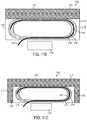
- FIG. 5shows a cross-sectional view of a sensor button switch assembly for a mobile communication device, according to aspects of embodiments of the disclosed subject matter
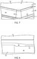
- FIG. 6shows a perspective view of a version of the sensor encapsulation assembly, according to aspects of embodiments of the disclosed subject matter
- FIG. 7shows a more detailed view of a portion of FIG. 6 ;
- FIG. 8shows a cross sectional view of an example of a transition from a sensor laminated package to a molded encapsulation, according to aspects of embodiments of the disclosed subject matter
- FIG. 9shows a cross-sectional view of a portion of FIG. 5 ;
- FIGS. 10A-Cshow a cross-sectional view of an embodiment of a button having a fingerprint sensor incorporated therein;
- FIGS. 11A-Cshow a cross-sectional view of another embodiment of a button having a fingerprint sensor incorporated therein;
- FIG. 12is a perspective view of a housing with a fingerprint sensor positioned therein;
- FIGS. 13A-Billustrate fingerprint sensors suitable for use with the button interfaces disclosed herein.
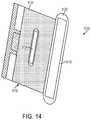
- FIG. 14is an illustration of a button having a fingerprint sensor incorporated therein.
- the sensor 10may be a biometric sensor, e.g., a fingerprint sensor having a plurality of pixel locations formed in either a linear one dimensional (“1D”) array or a two dimensional grid (“2D”) array, such as is shown schematically in FIG. 1 .
- the 2D sensor array 10may form a grid 20 , having transmit/drive signal vertical traces 30 and generally perpendicular horizontal receiver signal traces 32 .
- the sensor 10can also be seen to include a transmit/drive signal via section 40 to the top of the schematic illustration in FIG.
- each of the vias 44is electrically connected to a vertical trace 30 and each of the vias 46 is connected to a horizontal trace 32 , so that there are in reality many more traces 30 , 32 than illustrated in FIG. 1 .
- the grid 20would normally be about 12 mm in that direction and would have around 200 traces 32 .
- the perpendicular vertical traces 30aligned in the direction of the length of the finger, would be of the same pitch, but would be more in number, e.g., 600, though schematically in FIG. 1 the grid 20 is shown to be square.
- the grid 20could be of 200 horizontal traces 32 across the width of the finger and the vertical traces could be less than 200, e.g., a sufficient number to make the grid 20 a 12 mm ⁇ 4 mm grid array, by way of example, such as for a swipe sensor where the sensor captures so called frames of, e.g., from 66 horizontal traces, forming scanned frames that can be reconstructed to form the entire fingerprint image, as is well understood in the art.
- the disclosed subject mattercould support the packaging of a linear one dimensional capacitive gap array, where there are many vertical traces 30 but only one horizontal trace 32 , usually but not exclusively co-planer with the vertical traces 30 , and acting as a transmitter plate to the many perpendicular receiver plates 30 or a receiver plate to the many perpendicular transmitter plates 30 facing the single plate across a gap, e.g., forming a one dimensional linear capacitive gap array. It will also be understood that, as elsewhere discussed in the present application there is generally at least one layer between the horizontal traces 32 and the vertical traces 30 , in a 2D grid array, which layer(s) is not shown in FIG. 1 .
- FIG. 2shows in cross-section view a sensor support housing/package 100 , having a core layer 102 , having a thickness of about 100 ⁇ , ⁇ 20 ⁇ , an upper micro-printed circuit board (“PCB”) laminate layer 104 , having a thickness of about 75 ⁇ , ⁇ 10 ⁇ and a lower micro-PCB laminate layer 106 , having a thickness of about 75 ⁇ , ⁇ 10 ⁇ , on either side of the core layer 102 .
- PCBmicro-printed circuit board
- a transparent protective glass layer 120having a thickness of about 10 ⁇ , ⁇ 5 ⁇ , and an opaque ink rigid protective layer 122 , having a thickness of about 15 ⁇ , ⁇ 5 ⁇ along with an upper solder mask layer 130 , having a thickness of about 25 ⁇ , ⁇ 8 ⁇ are arranged above the upper micro-PCB laminate layer 104 .
- a lower solder mask layer 132having a thickness of about 25 ⁇ , ⁇ 8 ⁇ lies below the lower micro-PCB laminate layer 106 .
- PGApin grid array
- Upper micro-PCB laminate top traces 170may be formed partly in the upper micro-PCB laminate layer 104 and partly in the upper solder mask layer 130 .
- Upper micro-PCB laminate layer bottom traces 172may be formed, partly in the upper micro-PCB laminate layer 104 and partly in the core layer 102 .
- Lower micro-PCB laminate layer top traces 174may be formed partly in the lower micro-PCB laminate layer 106 and partly in the core layer 102 .
- Lower micro-PCB laminate bottom traces 176may be formed partly in the lower micro-PCB laminate layer 106 and partly in the lower solder mask layer 132 .
- Die connective pads 190may be formed on the back side of the integrated circuit die 140 , and have attached to each of them a die connective stud 192 , as can be seen in more detail, e.g., in FIG. 3 , which may be formed on the die 140 , e.g., through openings in a mask layer on the back side of the die 140 , which may later be removed.
- the studs 192may then be surrounded in the under fill layer 150 and serve to electrically connect a respective die connective pad 190 to a respective die connective stud 192 , which in turn connects through an opening 134 in the lower solder mask layer 132 to a respective lower micro-PCB laminate layer bottom trace 176 , e.g., through a bump 194 that may be grown on the respective stud 192 and formed, e.g., of solder.
- Core layer 102 vias 180e.g., connecting a respective upper micro-PCB laminate bottom trace 172 to a respective lower micro-PCB laminate top trace 174 may be formed through the core layer 102 , e.g., by laser drilling.
- Upper micro-PCB laminate layer vias 182e.g., connecting an upper micro-PCB laminate layer top trace 170 to a respective upper micro-PCB laminate bottom trace 172 , may similarly be formed through the upper micro-PCB laminate layer 104 .
- Lower micro-PCB laminate layer vias 184e.g., connecting a lower micro-PCB laminate top trace 174 to a respective lower micro-PCB laminate layer bottom trace 176 , may similarly be formed through the lower micro-PCB layer 106 .
- the die contact plates 190grown on the wafer substrate forming the die 140 , may be made of any suitable conductive material, such as aluminum (“Al”), copper (“Cu”) or gold (“Au”), while the contact studs 192 may also be made from a suitable conductive material, e.g., Cu.
- the contact bumps 194may be made, e.g., of solder and grown on the top of the contact posts 192 , after they are formed or while the masking material still covers the back side of the die 140 and may extend through openings 178 formed in the lower solder mask layer 132 .
- Ball grid array (“BGA”) solder balls 200may extend through openings 178 in the lower solder mask layer 132 and make electrical contact with lower micro-PCB laminate layer bottom traces 176 , e.g., to connect the package 100 to other electrical components of the sensor/imager 10 , e.g., through traces on a flexible or rigid substrate, e.g., 210 , as shown in FIGS. 5 and 9 , on which the package/housing 100 is mounted.
- BGABall grid array
- a flex substrate 210can be made from a suitable flexible and dielectric material, such as a polyimide film, like Kapton®.
- the top plan view of FIG. 4shows encapsulation material 220 encapsulating the package/housing 100 , as is shown in more detail in cross section in FIGS.
- the encapsulation material 220such as Mold Compound or any number of well known molding compounds, surrounding the package/housing 100 , and filling in around the BGA solder balls 200 , which may, e.g., make electrical contact to a trace(s) 208 on the flex material 210 .
- FIG. 5there in shown in cross section an example of an embodiment of a mobile device biometric sensor and switch combination 300 .
- the mobile device biometric sensor and switch combination 300fits within an opening 304 in a mobile device housing 302 , such that the upper sensor surface 222 , formed by the encapsulation material 220 of the housing is generally flush with the outer surface of the mobile device housing 302 .
- the encapsulated sensor package/housing 100may be mounted on a flexible substrate 210 , as shown in FIG. 9 that may be attached to a mobile device waterproof rubber seal member 310 , e.g., with a waterproof tape 320 .
- the sensor device package/housingmay be entirely encased in the encasing material as illustrated in FIG.
- a molded frame/spacer 240which may be made of the same material as the encapsulating material 220 , or, as shown in FIGS. 6-8 , may be molded in the encapsulation process.
- the spacer/frame 240may have a flange 280 , and may serve to hold the encapsulated package/housing 100 on the opening 302 .
- FIG. 8shows a cross-sectional view of a portion of an exemplary package/housing 100 within, e.g., a sensor encapsulation assembly, surrounded by encapsulation material 220 and covered by a relatively thin layer of rigid material 222 , applied as an ink originally and allowed to cure.
- the mounting of the package/housing 100 to the flex strip 210may give the entire assembly enough flexibility such that, when a finger or other object is pressed against the top of the housing, package 100 can move enough to operate an underlying mechanical switch, such as a dome switch 330 , which may include a depression member 322 and a deformable contact 332 .
- the switch 330may be connected to circuitry (not shown) on a circuit board 350 within the body of the mobile device.
- a toggling two position element 332may form the other contact of the switch 330 , such that when the depression member 322 is moved into the two position element it “clicks” to a non-contacting dome position and the switch 330 is open when the pressure on the package/housing is removed.
- a pair of stops 352 engaging the circuit board 350can insure the flex material does not bend to severely, thus damaging the relatively rigid package/housing 100 .
- An interposer plate 360attached to the bottom of the flexible strip 210 , can serve to move the depression member 322 , when downward pressure is put on the housing/package 100 .
- the spacer 240may be formed with a rounded edge 250 , to protect the finger of the user.
- the encapsulation materialmay be initially molded around the package/housing 100 to form, e.g., a slanted side wall 252 , rounded corners 260 the rounded top circumference 250 of the molded encapsulation, and the flange 280 .
- a slanted side wall 252e.g., a slanted side wall 252 , rounded corners 260 the rounded top circumference 250 of the molded encapsulation, and the flange 280 .
- the molded encapsulation material 220may be formed over a package housing 100 attacked to traces on the flexible material substrate 210 formed to have a trace extension 284 , which may serve to electrically connect the sensor 10 and IC 140 to other components of the system.
- the disclosed multi-layer laminate substrate technologyhas been employed to create a finger print sensor with a very durable package/housing construction, for biometrically authenticating a user of the mobile device and also suitable for use as part of a mobile device mechanical switch, e.g., for turning the mobile device on and off.
- the sensormay be formed of a 1D or 2D grid array of various shapes and sizes, with one dimension typically at least as wide as normal human finger.
- the gridcan be formed, as an example, by traces forming conducting leads on opposing sides of a top layer in a laminate of layers on opposing sides of a relatively rigid and strong, e.g., reinforced core layer.
- Electrical drive circuitrymay be connected to the traces on one side of the laminate layer and pick-up/response circuitry may be connected to the traces on the opposing side of the upper laminate layer, with the transmit drive traces typically formed closer to the sensing surface of the sensor, i.e., the top surface of the upper laminate layer.
- This top surface(top meaning surface closest to the finger during finger print acquisition), as noted, is usually configured as the transmitter traces and the other metal traces on the reverse side of the layer (farther away from the finger), layer is usually configured as the receiver. response signal traces.
- the traces formed in a 1D or 2D arrayconstitute pixel locations where the presence of the finger creates variations in the receive signal response to the transmitted signal, mostly due to variations in the capacitive coupling of the two through the finger near the top of the sensor 10 due to capacitive differences between the presence of a fingerprint valley or ridge in the vicinity of the given pixel location. These variations are detected to generate an finger print image either partly or wholly within the integrated circuit, which can also create the drive signals and time their application to drive signal traces in the grid 10 .
- the height of the package/housingcan vary based on the BGA size, e.g., in order to conform to differing height requirements.
- Package/housing sizecan, e.g., correspond to sensing linear array or grid array area, e.g., about 122 mm across in the direction of the width of the finger and the same or more in the direction of the length of the finger.
- the package bodycan, e.g., be square, e.g., in embodiments designed for housing the sensor on the top of or embedded within the housing as required to create a round button.
- the packagemay have some or all sides formed with a bevel cut package edge, e.g., down to about a 100 ⁇ depth, which may, e.g., be formed in a two pass singulation of individual packages/housings from a plurality of packages/housings formed in one operation as discussed elsewhere in the present application.
- a PCB or flex interposermay be required to make a housing in which the package/housing is part of actuating a mechanical switch button.
- Buttonsmay be manufactured, e.g., by placing a flex strip(s) in a molding jig.
- the button housingmay, e.g., be molded around the biometric sensor formed within the multilayer flip chip housing/package, e.g., with mold compound surrounding the flip chip placed on the flex strip, e.g., in a row of chips format.
- the flex stripmay form a substrate having, e.g., a thickness of around 80 ⁇ -120 ⁇ .
- the top portion of the mold materialmay have, e.g., a thickness of around 50 ⁇ and a bottom mold thickness of around 1 mm.
- a single sided molded package/housingmay be created, e.g., having a base substrate, which may be flexible, or rigid, e.g., a PCB or micro-laminated layer PCB, as discussed elsewhere in the present application, by way of illustration, by the mounting of a flip chip laminate package, described in the present application, to the substrate.
- the assembly, substrate plus flip chip laminate packagecan then be place entirely of mostly within an encapsulation material that may then be molded into a desired size and shape, e.g., by the use of moldable encapsulation material, such as well known molding compounds, plastics, resins, etc.
- the molding materialmay be used to fill under the flip chip package and/or around the perimeter and/or on the surface of the package to form a molded button.
- a molded buttonmay be utilized solely with the biometric sensor element to sense finger presence and/or surface movement, and, in response, act as a button, or may be combined with an interposer, such as made from a rigid material, like a PCB, or flexible, such as a flex substrate, e.g., to interact with an adjacent mechanical switch when the biometric, i.e., the finger presses down on the sensor area and thus on the entire package/housing.
- the substrate/interposer with a flip chip package attached, and encapsulated by use of injection/transfer/compression molding, or the like,may include on the sensing side an encapsulation thickness that is relatively thin, or even non-existent and selected and adjusted to establish a desired sensing distance from the surface of the actual sensing traces in the flip chip package. Sensing distance can be important to accurate data capture.
- the sensing side of the packagecan be encapsulated to protect the sensing area from surface, impact, or moisture damage. This can be done, by way of example, in a single molding step, by using materials with filler sizes appropriate for a top minimum thickness. In an example the minimum thickness over the flip chip package can be, e.g., 30-50 ⁇ . This thin layer of material would require the use of a fine filler, e.g. one with filler sizes of 15 ⁇ or smaller in the molding compound.
- the assemblycan also be encapsulated on all sides with the exception of the upper sensor surface.
- the sensor surfacecan be protected by applying protective coating, e.g., as noted elsewhere, a spray ink coating that hardens as it is cured, and/or a glass or other transparent plastic coating, of, e.g., by a second molding step.
- protective coatinge.g., as noted elsewhere, a spray ink coating that hardens as it is cured, and/or a glass or other transparent plastic coating, of, e.g., by a second molding step.
- the protective coating/coatings to the surface of an exposed flip chip laminate substrate and/or encapsulating areais contemplated.
- another variantmay be to add a protective coating/coatings to the surface of the flip chip package prior to assembly on the button substrate and further encapsulation.
- a protective coating/coatingsto the surface of the flip chip package prior to assembly on the button substrate and further encapsulation.
- Such an encapsulation molding processcan allow for a wide variety of customization of button sizes and shapes with a single flip chip package/housing by changing of the mold size and shape.
- Such encapsulation molding processing and materialscan also allow radius corners and edges that can not be as easily achieved with standard laminate package technologies.
- a low cost customizable finger print sensor buttone.g., for the mobile communication device market can be produced.
- the package/housing bodymay be, e.g., 10.5 mm ⁇ 4.0 mm.
- the package housingmay be mounted on a flexible substrate and with supporting components elsewhere on the substrate or on a rigid PCB or a mobile phone board. It is also possible for the flip chip package housing to be mounted to a motherboard with the specified other components also so mounted.
- a biometric sensormay comprise a plurality of a first type of signal traces formed on a first surface of a first layer of a multi-layer laminate package; at least one trace of a second type, formed on a second surface of the first layer or on a first surface of a second layer of the multi-layer laminate package; and connection vias in at least the first layer electrically connecting the signal traces of the first type or the signal traces of the second type to respective circuitry of the respective first or second type contained in an integrated circuit physically and electrically connected to one of the first layer, the second layer or a third layer of the multi-layer laminate package.
- the first type of signal tracemay comprise drive signal traces and the second type of traces may comprise at least one receive signal trace or the first type of traces comprising receive signal traces and the second type of traces comprising at least one drive signal trace.
- the at least one trace of the second typemay comprise one trace of the second type and the sensor may comprise a one dimensional linear array capacitive gap biometric sensor.
- the at least one trace of the second typemay comprise a plurality of traces of the second type and the sensor may comprise a two dimensional array capacitive biometric sensor.
- the first layermay comprise a circuit board layer and the second layer may comprise a core layer attached to one side of the circuit board layer.
- a third layer comprising a circuit board layermay be attached to another side of the core layer.
- the biometric sensormay be encapsulated on all sides except for a top finger sensing side and may be attached to a substrate.
- the biometric sensormay be encapsulated on all sides.
- the biometric sensormay be encapsulated by moldable plastic material formed around the package by a molding process, which also may form an encapsulation molded with rounded edges and corners.
- the biometric sensormay comprise a biometric sensor mounted on a portable electronic device, and may also cooperate mechanically with elements of a switch within the portable computing device to operate the switch.
- FIG. 10Ais a cross-sectional view of an embodiment of a button 1100 having a one dimensional (1D) or two dimensional (2D) biometric sensor 1130 , such as a chip on flex (COF) fingerprint sensor 1130 , incorporated therein.
- the button 1100can have an upper surface 1102 and a lower surface 1104 and may be configurable to provide, for example, a glass or suitable hard coat or film top layer 1110 having an upper surface 1112 and a lower surface 1114 , which can be surrounded by a housing 1120 on two or more sides. In this configuration, the edges of the top layer 1110 can be enclosed by a bezel 1122 , such as a rim that retains the top layer 1110 within the housing 1120 .
- a bezel 1122such as a rim that retains the top layer 1110 within the housing 1120 .
- the upper surface 1112 , of the top layer 1110can serve as an interface for a finger during use of the device and capture of biometric information from the user's finger.
- the top layer 1110can be configured to provide protection for the biometric sensor 1130 .
- the top layer 1110can be composed of different materials and/or colors which may also provide decorative identification. Additionally, the top layer 1110 can be formed from a hard material providing mechanical protection to the sensor tracer elements formed, e.g., on the flexible circuit substrate 1130 .
- the bottom portion of the housing 1120can also provide mechanical support for the button assembly 1100 .
- the housing 1120can be formed from, for example, polycarbonate (PC), acrylonitrile-butadiene-stryrene (ABS) or other suitable material, including any thermoplastic characterized by high-impact strength, as well as metals such as aluminum and titanium.
- the housing 1120can be configured to have a base 1124 , and parallel side walls 1126 (in two dimensional cross-section), an aperture 1128 can be provided through which flexible circuit substrate 1132 of the sensor 1130 passes to connect to the integrated circuit 1134 which can be positioned away from the housing 1120 .
- the top layer 1110can be formed from glass or any other suitable material such as shatter resistant substitutes for glass, including polymethylmethacrylate (PMMA), polyethylene terephthalate (PET), etc.
- the biometric sensor element substrate 1130can be formed from, for example, from a flexible circuit substrate formed with flex circuit metal tracer elements on top of a flexible film substrate 1132 with the metal traces being in electrical communication with an integrated circuit chip 1134 .
- the integrated circuit chip 1134need not form part of the stack of materials, and thus, in that configuration, can provide no mechanical functionality to the sensor/finger interface or mechanical operation of the button 1100 .
- An adhesive or potting material 1140 in the aperturesuch as thermo-setting plastic or silicone rubber gel, can be provided that secures and/or stabilizes the positioning of the sensor flexible circuit substrate 1130 , forming the sensor 1130 in a position between a bottom portion 1124 of the housing 1120 and the top layer 1110 which is engaged by the user during use.
- the adhesive or potting material 1140can consist of different regions or layers depending on the assembly method.
- the adhesive or potting material 1140may also consist of multiple adhesives or potting materials depending on assembly method and required properties of the button 1100 .
- Dimensions of the form factorcould be less than or equal to 900 mm 2 , less than or equal to 400 mm 2 , less than or equal to 225 mm 2 , less than or equal to 100 mm 2 , in a first two dimensional aspect.
- the thickness of the form factoris less than or equal to 2 mm or more preferably less than or equal to 1.5 mm. Further embodiments can have the form factor thickness less than or equal to 1 mm.
- the potting material 1140 in the openingcan be selected such that it provides mechanical support for the sensor 1130 .
- Impact resistance of the button 1100can be enhanced by maintaining a high hardness (modulus) throughout and/or thin adhesive thickness.
- the silicon integrated circuit (IC) chip 1134may not be included in this potting area to avoid thermal expansion, humidity expansion and general durability issues that might arise. That is to say, the flexible substrate 1138 can be unfolded from under the button 1100 , as illustrated, e.g., in FIG. 14 .
- biometric sensorscan include, for example, a fingerprint sensor, a velocity sensor, and an integrated circuit which is electrically connected to the fingerprint sensor and the velocity sensor. Biometric sensors can further include sensors adapted and configured to capture one or more parameters of, for example, a fingerprint. Conductive traces (not shown in FIG. 10A ) of an image sensor and velocity sensor can be etched or otherwise formed on a side of the flexible circuit substrate 1130 facing the upper surface 1112 of the button 1100 .
- the tracescan be positioned on the flexible substrate 1130 such that the traces are up (and thus on an upper surface 1136 of the substrate 1132 proximal to the top layer 1110 ), or the traces are down (and thus on a lower surface 1138 of the substrate distal the top layer 1110 ).
- the flex circuit 1130 on the flex substrate 1132can be configurable to have functionality (i.e., traces formed) on both the upper surface 1336 and the lower surface 1138 which enables the width of the flex 1130 to be reduced, and also reduces the overall package size.
- the button 1100can be part of a mechanically functional switch or a mechanically fixed button. Additionally, the button 1100 can be used for biometric sensing (fingerprint sensing), navigation, or touch sensing.
- the IC chip 1134need not be positioned within the stack of materials. Where the IC chip 1134 is positioned away from the stack of materials forming the button, the button 1100 can achieve a more compact profile and lower height which makes the button 1100 more adaptable to be incorporated into an electronic device, such as a smart phone or touch pad. Additionally, the configuration enables the properties (e.g., cover, adhesive material, housing) to be tuned for functionality and durability.
- propertiese.g., cover, adhesive material, housing
- a protective coatingcan be applied to the upper surface 1136 of the flex substrate 1132 itself, over the image sensor and velocity sensor to provide electrical isolation and mechanical protection of the sensors.
- conductive traces of an image sensorcan be formed on a bottom-side 1138 of a substrate 1132 , wherein the substrate 1132 of the flex circuit 1130 acts as a protective coating and can be further improved with a hard coating applied to the upper surface 1136 of the flex circuit 1130 itself.
- the senorcan be a 1D swipe sensor, a 2D touch sensor, a 2D motion sensor, a 2D sensor having two layers of electrodes, a 2D sensor having a single layer of electrodes, a 2D sensor with electrodes on either side of the flex substrate 1130 substrate.
- multiple conductor materialscan be used to form the sensor, such that different layers are made from different materials to achieve different results and for different reasons.
- the button 1100can be configurable such that it has a transparent interface, an opaque top coat, or a mask layer, and can be formed such that the upper surface material is not visually transparent. Additionally, the upper surface can be configurable such that it provides a variety of tactile interfaces, e.g., rough or smooth. An “anti-fingerprint and/or anti-smudge” (“AF”) and/or a hard coating can be applied.
- AFanti-fingerprint and/or anti-smudge”
- a hard coatingcan be applied.
- FIG. 10Bis a cross-sectional view of another configuration of a button 1100 ′ having a 1D or 2D biometric sensor, such as a COF fingerprint sensor, incorporated therein.
- the top layer 1110 ′formed from glass or any other suitable material such as shatter resistant substitutes for glass, including polymethylmethacrylate (PMMA), polyethylene terephthalate (PET), extends at least partly on top of some or all of the sides 1126 ′ of the housing 1120 ′.
- PMMApolymethylmethacrylate
- PETpolyethylene terephthalate
- FIG. 10Cis a cross-sectional view of another configuration of a button 1100 ′′ having a 1D or 2D biometric sensor, such as a COF fingerprint sensor, incorporated therein.
- the top layer 1110 ′′is over-molded which extends the top layer 1110 ′′ over and at least partly surrounds at least one side 1126 ′′ of the housing 1120 ′.
- This top layer 1110 ′′may be formed by over-molding, wet coating or any suitable method.
- FIG. 11Ais a cross-sectional view of another configuration of a button 2100 having a biometric sensor 2130 incorporated therein.
- the button 2100is configurable to provide, for example, a glass or suitable hard coat or film top layer 2110 which is surrounded by a housing 2120 .
- the housing 2120can be formed from polycarbonate (PC) or other suitable material including but not limited to metals such as aluminum.
- the biometric sensor 2130can be comprised, for example, from a flexible circuit substrate 2132 which is in electrical communication with an integrated circuit 2134 . This configuration is illustrated to have an adhesive or potting material, 2140 which may or may not be necessary depending on the method of manufacture.
- the flexible circuit 2132is secured and/or stabilized about an insert plate or support 2160 that can be fitted within the housing 2120 and, for example, clipped into place.
- the flexible circuit 2132wraps around the insert or plate 2160 and then the flex/plate combination can be clipped into the housing 2120 .
- the insert or platecan be clipped into the housing 2120 and then the flex substrate 2132 can be wrapped around the plate 2160 .
- the plate 2160may be placed into position within the housing 2120 using an adhesive, e.g., filling the opening 2140 , where the flex circuit 2130 fits instead of being clipped into place.
- Adhesive and/or potting materialsmay also be optionally used.
- the glass, hard coat or hard filmcan be bonded directly to the sensor flexible circuit 2130 flexible substrate 2132 or can be so bonded with an adhesive.
- FIG. 11Bis a cross-sectional view of another embodiment of a button 2100 ′ having a fingerprint sensor 2130 ′ incorporated therein.
- the button 2100 ′containing a flexible substrate 2132 ′ with the sensor elements 2130 ′ wrapped around an insert or plate 2160 ′ in electrical communication with the sensor IC 2134 ′ is configurable to provide, for example, a top layer 2110 ′ that extends at least partly on top of some or all of the sides 2126 ′ of the housing 2120 ′.
- FIG. 11Cis a cross-sectional view of another embodiment of a button 2100 ′ having a fingerprint sensor 2130 ′′ incorporated therein.
- the button 2100 ′′, containing a flexible substrate 2132 ′′ with the sensor elements 2130 ′′ wrapped around an insert or plate 2160 ′′ in electrical communication with the sensor IC 2134 ′′can be configurable to provide, for example, a top layer 2110 ′′ that extends over and at least partly surrounds at least one side of the housing, as shown, e.g., at 2112 ′′ on either side of the side walls 2126 ′′.
- This top layer 2110 ′′may be formed by over-molding, wet coating or any suitable method.
- FIG. 12is a perspective view of a button 3100 having a housing 3120 with a fingerprint sensor 3130 therein.
- FIGS. 13A-Billustrate fingerprint sensors 130 suitable for use with the button interfaces disclosed herein.
- Suitable 1D sensorspossess from 90 to 300 pixels, or more preferably from 114 to 200 pixels.
- Suitable 2D sensorspossess arrays of pixels in the range of 90 to 300 pixels by 90 to 300 pixels, or more preferentially a range of 114 to 200 pixels by 114 to 200 pixels.
- a sizeis from 8 to 30 mm across the broadest length, or more preferably from 6 to 20 mm.
- FIG. 13Aillustrates an example of a 2D touch sensor layout 4130 on flex;
- FIG. 13Billustrates an example of a 1D sensor layout 4130 ′ on flex.
- FIG. 14is an illustration that shows a top view of a button 5100 having a fingerprint sensor incorporated therein.
- the button 5100has a pill-shape profile as illustrated, but could be square or circular as required from the implementation.
- the biometric sensor elements 5130can be positioned within a portion of the housing 5120 and positioned to be attached to the top layer 5110 (same profile as housing 5120 ).
- the flexible substrate 5132can extend from the embedded sensor such that the substrate 5132 can be wrapped around, for example, a plate (not shown), or otherwise configured to fit within the housing 5120 .
- the integrated circuit 5134 which controls the operation of the sensor/button 5100is on an opposing end of the flexible substrate 5132 and in electrical communication with the sensor elements in the sensor/button 5100 .
- the button interfacesmay be housed in a host electronic device and configured to perform both object image capture and at least one of an activation of the host device, an activation of a host device function and an input to the host device.
- the button interfacesmay further comprise the button interfaces configured to allow a user to contact the switch simultaneously with providing object image data through an intersection of the at least one drive line and the at least one pickup line.
- the objectmay a finger and the button interfaces configured to sense a fingerprint image.
- the button interfaces described abovecan also be used to create a functional button (e.g., on/off), to provide navigation functionality, and/or to provide biometric sensing (such as fingerprint sensing).
- the buttonis manufactured according to the following:
- the buttonis manufactured according to the following:
- the buttonis manufactured according to the following:
- the buttonis manufactured according to the following:
- the manufacturing processis configurable to simplify the button manufacturing process using advanced manufacturing techniques while optimizing image capture through the molding compounds and/or layers.
Landscapes
- Engineering & Computer Science (AREA)
- Theoretical Computer Science (AREA)
- Physics & Mathematics (AREA)
- General Physics & Mathematics (AREA)
- Microelectronics & Electronic Packaging (AREA)
- General Engineering & Computer Science (AREA)
- Human Computer Interaction (AREA)
- Computer Hardware Design (AREA)
- Manufacturing & Machinery (AREA)
- Chemical & Material Sciences (AREA)
- Condensed Matter Physics & Semiconductors (AREA)
- Power Engineering (AREA)
- Ceramic Engineering (AREA)
- Multimedia (AREA)
- Electrochemistry (AREA)
- Health & Medical Sciences (AREA)
- Life Sciences & Earth Sciences (AREA)
- Analytical Chemistry (AREA)
- Biochemistry (AREA)
- General Health & Medical Sciences (AREA)
- Immunology (AREA)
- Pathology (AREA)
- Chemical Kinetics & Catalysis (AREA)
- Image Input (AREA)
- Measurement Of The Respiration, Hearing Ability, Form, And Blood Characteristics Of Living Organisms (AREA)
- Measurement Of Length, Angles, Or The Like Using Electric Or Magnetic Means (AREA)
Abstract
Description
- Singulate flex by, for example, laser cutting adjoining laminated material.
- ACF attach connection to flex may occur prior to singulating flex, after singulating flex or after final button assembly.
- Form housing, for example, using a cast or machine.
- Provide flex sensor with the ACF board.
- Flex bonded to housing.
- Assemble housing if needed.
- Form top layer either on the flex area only or on the housing only or both the flex and housing. The top layer could be a curable wet coat or cast or hard film bonded with adhesive among other materials.
- ACF attach connection to flex if not connected previously.
- Singulate flex.
- ACF attach connection to flex may occur prior to singulating flex, after singulating flex or after final button assembly.
- Form top layer on the flex area. The top layer could be a curable wet coat or cast or hard film bonded with adhesive among other materials. Applying top layer may occur prior to singulating flex.
- Flex bonded to housing.
- Housing assembled if needed.
- ACF attach connection to flex if not connected previously.
- Singulate flex.
- ACF attach connection to flex may occur prior to singulating flex, after singulating flex or after final button assembly.
- Top layer bonded to housing. The top layer could be a curable wet coat or cast or hard film bonded with adhesive among other materials.
- Bond flex to top layer and/or housing.
- Form support behind flex either by filling using an epoxy and/or bond plate in place.
- ACF attach connection to flex if not connected previously.
- Singulate flex.
- ACF attach connection to flex may occur prior to singulating flex, after singulating flex or after final button assembly.
- Attach flex to the bottom plate of the housing.
- Attach plate/flex combination to the housing.
- Attach top layer to the housing.
- Use adhesive or potting material if needed to fill volume.
- ACF attach connection to flex if not connected previously.
Claims (4)
Priority Applications (3)
| Application Number | Priority Date | Filing Date | Title |
|---|---|---|---|
| US16/399,074US11119615B2 (en) | 2012-10-14 | 2019-04-30 | Fingerprint sensor and button combinations and methods of making same |
| US17/400,504US11829565B2 (en) | 2012-10-14 | 2021-08-12 | Fingerprint sensor and button combinations and methods of making same |
| US18/492,829US12429988B2 (en) | 2012-10-14 | 2023-10-24 | Fingerprint sensor and button combinations and methods of making same |
Applications Claiming Priority (5)
| Application Number | Priority Date | Filing Date | Title |
|---|---|---|---|
| US201261713550P | 2012-10-14 | 2012-10-14 | |
| US201361754287P | 2013-01-18 | 2013-01-18 | |
| US14/050,012US9651513B2 (en) | 2012-10-14 | 2013-10-09 | Fingerprint sensor and button combinations and methods of making same |
| US15/489,561US10325132B2 (en) | 2012-10-14 | 2017-04-17 | Fingerprint sensor and button combinations and methods of making same |
| US16/399,074US11119615B2 (en) | 2012-10-14 | 2019-04-30 | Fingerprint sensor and button combinations and methods of making same |
Related Parent Applications (1)
| Application Number | Title | Priority Date | Filing Date |
|---|---|---|---|
| US15/489,561ContinuationUS10325132B2 (en) | 2012-10-14 | 2017-04-17 | Fingerprint sensor and button combinations and methods of making same |
Related Child Applications (1)
| Application Number | Title | Priority Date | Filing Date |
|---|---|---|---|
| US17/400,504ContinuationUS11829565B2 (en) | 2012-10-14 | 2021-08-12 | Fingerprint sensor and button combinations and methods of making same |
Publications (2)
| Publication Number | Publication Date |
|---|---|
| US20190258840A1 US20190258840A1 (en) | 2019-08-22 |
| US11119615B2true US11119615B2 (en) | 2021-09-14 |
Family
ID=50474814
Family Applications (4)
| Application Number | Title | Priority Date | Filing Date |
|---|---|---|---|
| US14/050,012Active2035-07-14US9651513B2 (en) | 2012-10-14 | 2013-10-09 | Fingerprint sensor and button combinations and methods of making same |
| US15/489,561Active2034-03-10US10325132B2 (en) | 2012-10-14 | 2017-04-17 | Fingerprint sensor and button combinations and methods of making same |
| US16/399,074Active2034-06-07US11119615B2 (en) | 2012-10-14 | 2019-04-30 | Fingerprint sensor and button combinations and methods of making same |
| US17/400,504Active2033-12-04US11829565B2 (en) | 2012-10-14 | 2021-08-12 | Fingerprint sensor and button combinations and methods of making same |
Family Applications Before (2)
| Application Number | Title | Priority Date | Filing Date |
|---|---|---|---|
| US14/050,012Active2035-07-14US9651513B2 (en) | 2012-10-14 | 2013-10-09 | Fingerprint sensor and button combinations and methods of making same |
| US15/489,561Active2034-03-10US10325132B2 (en) | 2012-10-14 | 2017-04-17 | Fingerprint sensor and button combinations and methods of making same |
Family Applications After (1)
| Application Number | Title | Priority Date | Filing Date |
|---|---|---|---|
| US17/400,504Active2033-12-04US11829565B2 (en) | 2012-10-14 | 2021-08-12 | Fingerprint sensor and button combinations and methods of making same |
Country Status (2)
| Country | Link |
|---|---|
| US (4) | US9651513B2 (en) |
| TW (1) | TWI578239B (en) |
Families Citing this family (64)
| Publication number | Priority date | Publication date | Assignee | Title |
|---|---|---|---|---|
| US9158958B2 (en) | 2010-10-28 | 2015-10-13 | Synaptics Incorporated | Signal strength enhancement in a biometric sensor array |
| US9152838B2 (en)* | 2012-03-29 | 2015-10-06 | Synaptics Incorporated | Fingerprint sensor packagings and methods |
| US9740343B2 (en) | 2012-04-13 | 2017-08-22 | Apple Inc. | Capacitive sensing array modulation |
| US9030440B2 (en) | 2012-05-18 | 2015-05-12 | Apple Inc. | Capacitive sensor packaging |
| US9651513B2 (en) | 2012-10-14 | 2017-05-16 | Synaptics Incorporated | Fingerprint sensor and button combinations and methods of making same |
| KR102204765B1 (en) | 2012-10-14 | 2021-01-19 | 시냅틱스 인코포레이티드 | Fingerprint sensor and button combinations and methods of making same |
| JP2014186847A (en)* | 2013-03-22 | 2014-10-02 | Fujitsu Ltd | Electronic apparatus |
| US9883822B2 (en) | 2013-06-05 | 2018-02-06 | Apple Inc. | Biometric sensor chip having distributed sensor and control circuitry |
| NL2012891B1 (en)* | 2013-06-05 | 2016-06-21 | Apple Inc | Biometric sensor chip having distributed sensor and control circuitry. |
| US9984270B2 (en) | 2013-08-05 | 2018-05-29 | Apple Inc. | Fingerprint sensor in an electronic device |
| US10296773B2 (en) | 2013-09-09 | 2019-05-21 | Apple Inc. | Capacitive sensing array having electrical isolation |
| US9460332B1 (en) | 2013-09-09 | 2016-10-04 | Apple Inc. | Capacitive fingerprint sensor including an electrostatic lens |
| US9697409B2 (en)* | 2013-09-10 | 2017-07-04 | Apple Inc. | Biometric sensor stack structure |
| KR101869624B1 (en) | 2013-11-22 | 2018-06-21 | 선전 구딕스 테크놀로지 컴퍼니, 리미티드 | Secure human fingerprint sensor |
| WO2015081326A1 (en) | 2013-11-27 | 2015-06-04 | Shenzhen Huiding Technology Co., Ltd. | Wearable communication devices for secured transaction and communication |
| US10128907B2 (en)* | 2014-01-09 | 2018-11-13 | Shenzhen GOODIX Technology Co., Ltd. | Fingerprint sensor module-based device-to-device communication |
| US10051724B1 (en)* | 2014-01-31 | 2018-08-14 | Apple Inc. | Structural ground reference for an electronic component of a computing device |
| KR20150099295A (en)* | 2014-02-21 | 2015-08-31 | 삼성전자주식회사 | Electronic device including a physical key |
| US20150296622A1 (en)* | 2014-04-11 | 2015-10-15 | Apple Inc. | Flexible Printed Circuit With Semiconductor Strain Gauge |
| KR20160129874A (en) | 2014-07-07 | 2016-11-09 | 선전 후이딩 테크놀로지 컴퍼니 리미티드 | Integration of touch screen and fingerprint sensor assembly |
| TWM493712U (en)* | 2014-08-01 | 2015-01-11 | Superc Touch Corp | Biometric recognition device having inductive electrode with mask function |
| WO2016036046A1 (en)* | 2014-09-03 | 2016-03-10 | 크루셜텍(주) | Fingerprint sensor module and manufacturing method therefor |
| TWI570857B (en)* | 2014-12-10 | 2017-02-11 | 矽品精密工業股份有限公司 | Package structure and method for manufacturing the same |
| KR101675465B1 (en)* | 2015-01-02 | 2016-11-15 | 주식회사 바이오메트릭스 | Biometrics sensor module including film cover and packaging method of biometrics sensor |
| TWI594341B (en) | 2015-01-19 | 2017-08-01 | 神盾股份有限公司 | Fingerprint sensor package and method for fabricating the same |
| TWI531980B (en)* | 2015-01-19 | 2016-05-01 | 致伸科技股份有限公司 | A method of producing sensing device |
| KR102348486B1 (en)* | 2015-04-29 | 2022-01-07 | 삼성전자 주식회사 | Electronic device |
| USD776664S1 (en)* | 2015-05-20 | 2017-01-17 | Chaya Coleena Hendrick | Smart card |
| US10043049B2 (en) | 2015-06-08 | 2018-08-07 | Fingerprint Cards Ab | Fingerprint sensing device with heterogeneous coating structure comprising a dielectric material |
| TW201643772A (en)* | 2015-06-08 | 2016-12-16 | 指紋卡公司 | Fingerprint sensing device with interposer structure |
| US9842243B2 (en)* | 2015-06-08 | 2017-12-12 | Fingerprint Cards Ab | Fingerprint sensing device with heterogeneous coating structure comprising a mold |
| CN105528104A (en)* | 2015-07-03 | 2016-04-27 | 宸鸿科技(厦门)有限公司 | A touch control panel having a fingerprint identification function and a method for manufacturing the same |
| US20170047276A1 (en)* | 2015-08-13 | 2017-02-16 | Advanced Semiconductor Engineering, Inc. | Semiconductor device package and method of manufacturing the same |
| US9785821B2 (en) | 2015-08-28 | 2017-10-10 | Synaptics Incorporated | Capacitive sensor architecture for biometric sensing |
| US10055631B1 (en)* | 2015-11-03 | 2018-08-21 | Synaptics Incorporated | Semiconductor package for sensor applications |
| US9898645B2 (en) | 2015-11-17 | 2018-02-20 | Taiwan Semiconductor Manufacturing Company, Ltd. | Fingerprint sensor device and method |
| WO2017085669A2 (en) | 2015-11-20 | 2017-05-26 | Idex Asa | Electronic sensor supported on rigid substrate |
| US9792516B2 (en) | 2016-01-26 | 2017-10-17 | Next Biometrics Group Asa | Flexible card with fingerprint sensor |
| JP6751359B2 (en)* | 2016-01-27 | 2020-09-02 | 株式会社ジャパンディスプレイ | Fingerprint detector |
| US9904776B2 (en) | 2016-02-10 | 2018-02-27 | Taiwan Semiconductor Manufacturing Company, Ltd. | Fingerprint sensor pixel array and methods of forming same |
| US10256173B2 (en)* | 2016-02-22 | 2019-04-09 | Advanced Semiconductor Engineering, Inc. | Semiconductor device and method for manufacturing the same |
| US9939920B2 (en) | 2016-03-03 | 2018-04-10 | Microsoft Technology Licensing, Llc | Keyset fingerprint sensor with backlight |
| KR102622021B1 (en) | 2016-08-03 | 2024-01-08 | 삼성전자 주식회사 | Electronic device having finger print sensor |
| TWI582704B (en)* | 2016-08-05 | 2017-05-11 | Primax Electronics Ltd | Mrthod for fabricating fingerprint identifying module |
| US10248251B2 (en)* | 2016-08-16 | 2019-04-02 | Guangdong Oppo Mobile Telecommunications Corp. | Method for manufacturing input assembly, input assembly and terminal |
| US10055637B2 (en) | 2016-12-07 | 2018-08-21 | Synaptics Incorporated | Optical sensor with substrate light filter |
| TWI672779B (en)* | 2016-12-28 | 2019-09-21 | 曦威科技股份有限公司 | Fingerprint identification device, mobile device using the same and method for manufacturing fingerprint identification device |
| WO2018138651A1 (en) | 2017-01-24 | 2018-08-02 | Idex Asa | Configurable, encapsulated sensor module and method for making same |
| US11003883B2 (en)* | 2017-03-07 | 2021-05-11 | The Regents Of The University Of California | Adjustable fingerprint capturing device |
| US10866619B1 (en) | 2017-06-19 | 2020-12-15 | Apple Inc. | Electronic device having sealed button biometric sensing system |
| EP3451804B1 (en) | 2017-08-28 | 2020-04-01 | Goodrich Actuation Systems Limited | Potting method |
| US10509936B2 (en)* | 2017-08-28 | 2019-12-17 | Superc-Touch Corporation | Fingerprint identification apparatus having conductive structure |
| TWI628600B (en)* | 2017-09-12 | 2018-07-01 | 速博思股份有限公司 | Electronic apparatus with embedded fingerprint sensing module |
| CN111344714B (en) | 2017-09-19 | 2022-03-25 | 傲迪司威生物识别公司 | Two-sided sensor module suitable for integration into an electronic device |
| US11275920B1 (en) | 2017-09-27 | 2022-03-15 | Apple Inc. | Elongated fingerprint sensor |
| JP6942023B2 (en)* | 2017-10-10 | 2021-09-29 | 株式会社東海理化電機製作所 | Switch device |
| SE1751447A1 (en) | 2017-11-24 | 2019-05-25 | Fingerprint Cards Ab | Cost-efficient fingerprint sensor component and manufacturing method |
| KR102445512B1 (en)* | 2018-03-30 | 2022-09-21 | 삼성디스플레이 주식회사 | Fingerprint sensor package and display device including same |
| US11187721B2 (en)* | 2020-02-03 | 2021-11-30 | Sunasic Technologies, Inc. | Contactor for testing electronic device |
| US11689834B2 (en) | 2020-04-02 | 2023-06-27 | Apple Inc. | Portable electronic device |
| US11189248B1 (en) | 2020-05-06 | 2021-11-30 | Apple Inc. | Systems and methods for switching vision correction graphical outputs on a display of an electronic device |
| US12093359B2 (en) | 2020-09-25 | 2024-09-17 | Apple Inc. | Electronic device having a sealed biometric input system |
| US11783629B2 (en) | 2021-03-02 | 2023-10-10 | Apple Inc. | Handheld electronic device |
| CN113425269B (en)* | 2021-07-16 | 2024-12-27 | 维沃移动通信有限公司 | Method, device and electronic device for measuring biometric information |
Citations (55)
| Publication number | Priority date | Publication date | Assignee | Title |
|---|---|---|---|---|
| US4851862A (en)* | 1988-08-05 | 1989-07-25 | Eastman Kodak Company | Led array printhead with tab bonded wiring |
| US5400219A (en)* | 1992-09-02 | 1995-03-21 | Eastman Kodak Company | Tape automated bonding for electrically connecting semiconductor chips to substrates |
| US5748441A (en) | 1995-06-22 | 1998-05-05 | Siemens Aktiengesellschaft | Notepad computer having an integrated video camera |
| US6188391B1 (en) | 1998-07-09 | 2001-02-13 | Synaptics, Inc. | Two-layer capacitive touchpad and method of making same |
| US6337919B1 (en) | 1999-04-28 | 2002-01-08 | Intel Corporation | Fingerprint detecting mouse |
| JP2002330202A (en) | 2001-05-02 | 2002-11-15 | Sony Corp | Portable terminal equipment with built-in fingerprint sensor |
| US20030012882A1 (en)* | 2000-02-01 | 2003-01-16 | Kiwamu Tokuhisa | Adhesive polyimide resin and adhesive laminate |
| US6522773B1 (en) | 1998-03-03 | 2003-02-18 | Siemens Aktiengesellschaft | Fingertip sensor with integrated key switch |
| US20030063445A1 (en) | 2000-03-24 | 2003-04-03 | Reinhard Fischbach | Housing for biometric sensor chips and method for producing the housing |
| US20030107118A1 (en)* | 2001-10-09 | 2003-06-12 | Tessera, Inc. | Stacked packages |
| US20030201524A1 (en)* | 2002-04-24 | 2003-10-30 | Yukihiro Murakami | Tape automated bonding with strip carrier frame assembly |
| US6710461B2 (en) | 2002-06-06 | 2004-03-23 | Lightuning Tech. Inc. | Wafer level packaging of micro electromechanical device |
| US20040123113A1 (en) | 2002-12-18 | 2004-06-24 | Svein Mathiassen | Portable or embedded access and input devices and methods for giving access to access limited devices, apparatuses, appliances, systems or networks |
| US6795569B1 (en) | 1999-05-11 | 2004-09-21 | Authentec, Inc. | Fingerprint image compositing method and associated apparatus |
| US6912299B1 (en) | 1998-02-18 | 2005-06-28 | Nec Corporation | Device for detecting a fingerprint, electric apparatus and doorkeeper apparatus |
| US6950541B1 (en) | 1999-05-11 | 2005-09-27 | Authentec, Inc. | Fingerprint sensor package including flexible circuit substrate and associated methods |
| US7030860B1 (en) | 1999-10-08 | 2006-04-18 | Synaptics Incorporated | Flexible transparent touch sensing system for electronic devices |
| US20060140461A1 (en) | 2004-12-29 | 2006-06-29 | Lg Electronics Inc. | Mobile communication device having fingerprint recognition sensor |
| US20070086630A1 (en) | 2005-10-18 | 2007-04-19 | Authentec, Inc. | Finger sensor including flexible circuit and associated methods |
| US7251351B2 (en) | 2000-06-09 | 2007-07-31 | Idex Asa | Sensor unit, especially for fingerprint sensors |
| CN101034432A (en) | 2006-03-10 | 2007-09-12 | 敦南科技股份有限公司 | Packaging structure and packaging method of ultra-thin optical fingerprint interception module |
| US20070259515A1 (en)* | 2006-05-04 | 2007-11-08 | Korea Advanced Institute Of Science And Technology | Method for manufacturing wafer-level packages for flip chips capable of preventing adhesives from absorbing water |
| US20080049980A1 (en) | 2006-08-28 | 2008-02-28 | Motorola, Inc. | Button with integrated biometric sensor |
| US20080054875A1 (en) | 2006-09-01 | 2008-03-06 | Ivi Smart Technologies, Inc. | Biometric sensor and sensor panel |
| US7417310B2 (en) | 2006-11-02 | 2008-08-26 | Entorian Technologies, Lp | Circuit module having force resistant construction |
| US20080238878A1 (en) | 2007-03-30 | 2008-10-02 | Pi-Hui Wang | Pointing device using fingerprint |
| TW200919255A (en) | 2007-09-24 | 2009-05-01 | Apple Inc | Embedded authentication systems in an electronic device |
| US20090153791A1 (en)* | 2007-12-12 | 2009-06-18 | Au Optronics Corp. | Chip on film structure |
| US20090257626A1 (en) | 2005-10-18 | 2009-10-15 | Authentec, Inc. | Thinned finger sensor and associated methods |
| US20090288680A1 (en)* | 2008-05-21 | 2009-11-26 | Canon Kabushiki Kaisha | Method for producing organic light-emitting device |
| CN1983336B (en) | 2005-12-16 | 2010-08-18 | 四川新龙门阵文化传播有限公司 | System for realizing transaction service by cell-phone |
| US20100220900A1 (en) | 2009-03-02 | 2010-09-02 | Avago Technologies Ecbu Ip (Singapore) Pte. Ltd. | Fingerprint sensing device |
| US20100259503A1 (en) | 2009-04-10 | 2010-10-14 | Nec Lcd Technologies, Ltd. | Touch sensor device and electronic apparatus having the same |
| US20100321159A1 (en) | 2009-06-18 | 2010-12-23 | Authentec, Inc. | Touch based data communication using biometric finger sensor and associated methods |
| US20100321158A1 (en) | 2009-06-19 | 2010-12-23 | Authentec, Inc. | Finger sensor having remote web based notifications |
| CN101933051A (en) | 2008-01-29 | 2010-12-29 | 高通股份有限公司 | Systems and methods for accessing a tamperproof storage device in a wireless communication device using biometric data |
| TW201113992A (en) | 2009-10-07 | 2011-04-16 | Xintec Inc | Chip package and fabrication method thereof |
| US20110090047A1 (en) | 2001-02-20 | 2011-04-21 | Patel Pankaj B | Biometric switch and indicating means |
| US20110175703A1 (en) | 2010-01-15 | 2011-07-21 | Benkley Iii Fred G | Electronic Imager Using an Impedance Sensor Grid Array Mounted on or about a Switch and Method of Making |
| US20110215484A1 (en) | 2010-03-05 | 2011-09-08 | Upek, Inc. | Integrally Molded Die And Bezel Structure For Fingerprint Sensors And The Like |
| US8018065B2 (en) | 2008-02-28 | 2011-09-13 | Atmel Corporation | Wafer-level integrated circuit package with top and bottom side electrical connections |
| US20110298711A1 (en) | 2010-06-02 | 2011-12-08 | Validity Sensors, Inc. | Integrated Fingerprint Sensor and Navigation Device |
| US20110304001A1 (en) | 2010-02-19 | 2011-12-15 | Validity Sensors, Inc. | Fingerprint sensing circuit |
| US20110309482A1 (en) | 2010-06-18 | 2011-12-22 | Authentec, Inc. | Finger sensor including encapsulating layer over sensing area and related methods |
| US20110316146A1 (en)* | 2010-06-24 | 2011-12-29 | Stats Chippac, Ltd. | Semiconductor Device and Method of Forming Anisotropic Conductive Film Between Semiconductor Die and Build-Up Interconnect Structure |
| US20120134549A1 (en) | 2010-01-15 | 2012-05-31 | Picofield Technologies Inc. | Biometric Image Sensing |
| US20120256280A1 (en) | 2011-03-16 | 2012-10-11 | Richard Alexander Erhart | Packaging for fingerprint sensors and methods of manufacture |
| GB2496055A (en) | 2011-10-27 | 2013-05-01 | Validity Sensors Inc | Fingerprint sensor integrated with an electronic device |
| US20130181949A1 (en) | 2012-01-17 | 2013-07-18 | Apple Inc. | Finger sensor having pixel sensing circuitry for coupling electrodes and pixel sensing traces and related methods |
| US20130259329A1 (en) | 2012-03-29 | 2013-10-03 | Validity Sensors, Inc. | Fingerprint sensor packagings and methods |
| US20130279769A1 (en) | 2012-04-10 | 2013-10-24 | Picofield Technologies Inc. | Biometric Sensing |
| US20130307818A1 (en)* | 2012-05-18 | 2013-11-21 | Apple Inc. | Capacitive Sensor Packaging |
| US20130308838A1 (en)* | 2012-05-18 | 2013-11-21 | Apple Inc. | Efficient Texture Comparison |
| US20140103943A1 (en) | 2012-10-14 | 2014-04-17 | Synaptics Incorporated | Fingerprint sensor and button combinations and methods of making same |
| US8701267B2 (en) | 2010-11-05 | 2014-04-22 | Authentec, Inc. | Method of making a finger sensor package |
Family Cites Families (8)
| Publication number | Priority date | Publication date | Assignee | Title |
|---|---|---|---|---|
| DE69922722T2 (en)* | 1998-03-05 | 2005-12-15 | Nippon Telegraph And Telephone Corp. | Surface shape recognition sensor and its manufacturing method |
| WO2004093505A2 (en)* | 2003-04-15 | 2004-10-28 | Wavezero, Inc. | Emi shielding for electronic component packaging |
| JP2005030901A (en)* | 2003-07-11 | 2005-02-03 | Alps Electric Co Ltd | Capacitive sensor |
| JP4466314B2 (en)* | 2004-10-20 | 2010-05-26 | パナソニック株式会社 | Push-on switch |
| US7204018B2 (en)* | 2004-12-16 | 2007-04-17 | Nortel Networks Limited | Technique for reducing via capacitance |
| US8309523B2 (en)* | 2007-11-21 | 2012-11-13 | Vib Vzw | Inhibitors of MALT1 proteolytic activity and uses thereof |
| US7808101B2 (en)* | 2008-02-08 | 2010-10-05 | Fairchild Semiconductor Corporation | 3D smart power module |
| NO20093601A1 (en)* | 2009-12-29 | 2011-06-30 | Idex Asa | surface Sensor |
- 2013
- 2013-10-09USUS14/050,012patent/US9651513B2/enactiveActive
- 2013-10-14TWTW102136931Apatent/TWI578239B/enactive
- 2017
- 2017-04-17USUS15/489,561patent/US10325132B2/enactiveActive
- 2019
- 2019-04-30USUS16/399,074patent/US11119615B2/enactiveActive
- 2021
- 2021-08-12USUS17/400,504patent/US11829565B2/enactiveActive
Patent Citations (58)
| Publication number | Priority date | Publication date | Assignee | Title |
|---|---|---|---|---|
| US4851862A (en)* | 1988-08-05 | 1989-07-25 | Eastman Kodak Company | Led array printhead with tab bonded wiring |
| US5400219A (en)* | 1992-09-02 | 1995-03-21 | Eastman Kodak Company | Tape automated bonding for electrically connecting semiconductor chips to substrates |
| US5748441A (en) | 1995-06-22 | 1998-05-05 | Siemens Aktiengesellschaft | Notepad computer having an integrated video camera |
| US6912299B1 (en) | 1998-02-18 | 2005-06-28 | Nec Corporation | Device for detecting a fingerprint, electric apparatus and doorkeeper apparatus |
| US6522773B1 (en) | 1998-03-03 | 2003-02-18 | Siemens Aktiengesellschaft | Fingertip sensor with integrated key switch |
| US6188391B1 (en) | 1998-07-09 | 2001-02-13 | Synaptics, Inc. | Two-layer capacitive touchpad and method of making same |
| US6337919B1 (en) | 1999-04-28 | 2002-01-08 | Intel Corporation | Fingerprint detecting mouse |
| US6795569B1 (en) | 1999-05-11 | 2004-09-21 | Authentec, Inc. | Fingerprint image compositing method and associated apparatus |
| US6950541B1 (en) | 1999-05-11 | 2005-09-27 | Authentec, Inc. | Fingerprint sensor package including flexible circuit substrate and associated methods |
| US7030860B1 (en) | 1999-10-08 | 2006-04-18 | Synaptics Incorporated | Flexible transparent touch sensing system for electronic devices |
| US20030012882A1 (en)* | 2000-02-01 | 2003-01-16 | Kiwamu Tokuhisa | Adhesive polyimide resin and adhesive laminate |
| US20030063445A1 (en) | 2000-03-24 | 2003-04-03 | Reinhard Fischbach | Housing for biometric sensor chips and method for producing the housing |
| US7848550B2 (en) | 2000-06-09 | 2010-12-07 | Idex Asa | Sensor unit, especially for fingerprint sensors |
| US7251351B2 (en) | 2000-06-09 | 2007-07-31 | Idex Asa | Sensor unit, especially for fingerprint sensors |
| US20110090047A1 (en) | 2001-02-20 | 2011-04-21 | Patel Pankaj B | Biometric switch and indicating means |
| JP2002330202A (en) | 2001-05-02 | 2002-11-15 | Sony Corp | Portable terminal equipment with built-in fingerprint sensor |
| US20030107118A1 (en)* | 2001-10-09 | 2003-06-12 | Tessera, Inc. | Stacked packages |
| US20030201524A1 (en)* | 2002-04-24 | 2003-10-30 | Yukihiro Murakami | Tape automated bonding with strip carrier frame assembly |
| US6710461B2 (en) | 2002-06-06 | 2004-03-23 | Lightuning Tech. Inc. | Wafer level packaging of micro electromechanical device |
| US20040123113A1 (en) | 2002-12-18 | 2004-06-24 | Svein Mathiassen | Portable or embedded access and input devices and methods for giving access to access limited devices, apparatuses, appliances, systems or networks |
| US20060140461A1 (en) | 2004-12-29 | 2006-06-29 | Lg Electronics Inc. | Mobile communication device having fingerprint recognition sensor |
| US20090257626A1 (en) | 2005-10-18 | 2009-10-15 | Authentec, Inc. | Thinned finger sensor and associated methods |
| US20070086630A1 (en) | 2005-10-18 | 2007-04-19 | Authentec, Inc. | Finger sensor including flexible circuit and associated methods |
| CN1983336B (en) | 2005-12-16 | 2010-08-18 | 四川新龙门阵文化传播有限公司 | System for realizing transaction service by cell-phone |
| CN101034432A (en) | 2006-03-10 | 2007-09-12 | 敦南科技股份有限公司 | Packaging structure and packaging method of ultra-thin optical fingerprint interception module |
| US20070259515A1 (en)* | 2006-05-04 | 2007-11-08 | Korea Advanced Institute Of Science And Technology | Method for manufacturing wafer-level packages for flip chips capable of preventing adhesives from absorbing water |
| US20080049980A1 (en) | 2006-08-28 | 2008-02-28 | Motorola, Inc. | Button with integrated biometric sensor |
| US20080054875A1 (en) | 2006-09-01 | 2008-03-06 | Ivi Smart Technologies, Inc. | Biometric sensor and sensor panel |
| US8786033B2 (en) | 2006-09-01 | 2014-07-22 | IVI Holdings, Ltd. | Biometric sensor and sensor panel, method for detecting biometric pattern using the same, and method for manufacturing the same |
| US7417310B2 (en) | 2006-11-02 | 2008-08-26 | Entorian Technologies, Lp | Circuit module having force resistant construction |
| US20080238878A1 (en) | 2007-03-30 | 2008-10-02 | Pi-Hui Wang | Pointing device using fingerprint |
| TW200919255A (en) | 2007-09-24 | 2009-05-01 | Apple Inc | Embedded authentication systems in an electronic device |
| US20090153791A1 (en)* | 2007-12-12 | 2009-06-18 | Au Optronics Corp. | Chip on film structure |
| CN101933051A (en) | 2008-01-29 | 2010-12-29 | 高通股份有限公司 | Systems and methods for accessing a tamperproof storage device in a wireless communication device using biometric data |
| US8018065B2 (en) | 2008-02-28 | 2011-09-13 | Atmel Corporation | Wafer-level integrated circuit package with top and bottom side electrical connections |
| US20090288680A1 (en)* | 2008-05-21 | 2009-11-26 | Canon Kabushiki Kaisha | Method for producing organic light-emitting device |
| US20100220900A1 (en) | 2009-03-02 | 2010-09-02 | Avago Technologies Ecbu Ip (Singapore) Pte. Ltd. | Fingerprint sensing device |
| US20100259503A1 (en) | 2009-04-10 | 2010-10-14 | Nec Lcd Technologies, Ltd. | Touch sensor device and electronic apparatus having the same |
| US20100321159A1 (en) | 2009-06-18 | 2010-12-23 | Authentec, Inc. | Touch based data communication using biometric finger sensor and associated methods |
| US20100321158A1 (en) | 2009-06-19 | 2010-12-23 | Authentec, Inc. | Finger sensor having remote web based notifications |
| TW201113992A (en) | 2009-10-07 | 2011-04-16 | Xintec Inc | Chip package and fabrication method thereof |
| US20110175703A1 (en) | 2010-01-15 | 2011-07-21 | Benkley Iii Fred G | Electronic Imager Using an Impedance Sensor Grid Array Mounted on or about a Switch and Method of Making |
| US20120134549A1 (en) | 2010-01-15 | 2012-05-31 | Picofield Technologies Inc. | Biometric Image Sensing |
| US20110304001A1 (en) | 2010-02-19 | 2011-12-15 | Validity Sensors, Inc. | Fingerprint sensing circuit |
| US20110215484A1 (en) | 2010-03-05 | 2011-09-08 | Upek, Inc. | Integrally Molded Die And Bezel Structure For Fingerprint Sensors And The Like |
| US20110298711A1 (en) | 2010-06-02 | 2011-12-08 | Validity Sensors, Inc. | Integrated Fingerprint Sensor and Navigation Device |
| US20110309482A1 (en) | 2010-06-18 | 2011-12-22 | Authentec, Inc. | Finger sensor including encapsulating layer over sensing area and related methods |
| US8736001B2 (en) | 2010-06-18 | 2014-05-27 | Authentec, Inc. | Finger sensor including encapsulating layer over sensing area and related methods |
| US20110316146A1 (en)* | 2010-06-24 | 2011-12-29 | Stats Chippac, Ltd. | Semiconductor Device and Method of Forming Anisotropic Conductive Film Between Semiconductor Die and Build-Up Interconnect Structure |
| US8701267B2 (en) | 2010-11-05 | 2014-04-22 | Authentec, Inc. | Method of making a finger sensor package |
| US20120256280A1 (en) | 2011-03-16 | 2012-10-11 | Richard Alexander Erhart | Packaging for fingerprint sensors and methods of manufacture |
| GB2496055A (en) | 2011-10-27 | 2013-05-01 | Validity Sensors Inc | Fingerprint sensor integrated with an electronic device |
| US20130181949A1 (en) | 2012-01-17 | 2013-07-18 | Apple Inc. | Finger sensor having pixel sensing circuitry for coupling electrodes and pixel sensing traces and related methods |
| US20130259329A1 (en) | 2012-03-29 | 2013-10-03 | Validity Sensors, Inc. | Fingerprint sensor packagings and methods |
| US20130279769A1 (en) | 2012-04-10 | 2013-10-24 | Picofield Technologies Inc. | Biometric Sensing |
| US20130307818A1 (en)* | 2012-05-18 | 2013-11-21 | Apple Inc. | Capacitive Sensor Packaging |
| US20130308838A1 (en)* | 2012-05-18 | 2013-11-21 | Apple Inc. | Efficient Texture Comparison |
| US20140103943A1 (en) | 2012-10-14 | 2014-04-17 | Synaptics Incorporated | Fingerprint sensor and button combinations and methods of making same |
Non-Patent Citations (3)
| Title |
|---|
| Hyoung-Joon Kim et al., "Study on bubble formation in rigid-flexible substrates bonding using anisotropic conductive films (ACFs) and their effects on the ACF joint reliability," 56th Electronic Components and Technology Conference 2006 (Year: 2006).* |
| Taiwan Patent Office Search Report; Taiwan Application No. 102111264; dated Apr. 29, 2016. |
| Taiwan Patent Office Search Report; Taiwan Application No. 102136931; dated Nov. 23, 2016. |
Also Published As
| Publication number | Publication date |
|---|---|
| TW201428639A (en) | 2014-07-16 |
| US20170220837A1 (en) | 2017-08-03 |
| US20190258840A1 (en) | 2019-08-22 |
| US20140103943A1 (en) | 2014-04-17 |
| US10325132B2 (en) | 2019-06-18 |
| TWI578239B (en) | 2017-04-11 |
| US9651513B2 (en) | 2017-05-16 |
| US20210373709A1 (en) | 2021-12-02 |
| US11829565B2 (en) | 2023-11-28 |
Similar Documents
| Publication | Publication Date | Title |
|---|---|---|
| US11829565B2 (en) | Fingerprint sensor and button combinations and methods of making same | |
| CN108229340B (en) | Fingerprint sensing module and manufacturing method thereof, and smart card and manufacturing method thereof | |
| US10445548B2 (en) | Fingerprint sensing assemblies and methods of making | |
| KR101503183B1 (en) | Finger sensor including encapsulating layer over sensing area and related methods | |
| CN105404880B (en) | Electronic device with fingerprint sensor assembly | |
| JP2010103240A (en) | Contact sensor unit, electronic device, and method for manufacturing the contact sensor unit | |
| CN104134063A (en) | Fingerprint identification and detection assembly and electronic device of fingerprint identification and detection assembly | |
| KR102022708B1 (en) | Fingerprint sensor module and method for manufacturing the same | |
| KR20140123919A (en) | Fingerprint sensor module, portable electronic device having the same, and manufacturing method thereof | |
| EP3836010B1 (en) | A biometric sensor module for card integration | |
| WO2012061559A1 (en) | Method of making a finger sensor package and associated devices | |
| KR20160091493A (en) | Fingerprint sensor module and manufacturing method thereof | |
| US12429988B2 (en) | Fingerprint sensor and button combinations and methods of making same | |
| KR101613084B1 (en) | Fingerprint sensor module and portable electronic device having the same | |
| US20170192542A1 (en) | Track pad semiconductor package using compression molding and method for manufacturing the same |
Legal Events
| Date | Code | Title | Description |
|---|---|---|---|
| FEPP | Fee payment procedure | Free format text:ENTITY STATUS SET TO UNDISCOUNTED (ORIGINAL EVENT CODE: BIG.); ENTITY STATUS OF PATENT OWNER: LARGE ENTITY | |
| AS | Assignment | Owner name:SYNAPTICS INCORPORATED, CALIFORNIA Free format text:ASSIGNMENT OF ASSIGNORS INTEREST;ASSIGNOR:VALIDITY SENSORS, LLC;REEL/FRAME:049058/0256 Effective date:20131217 Owner name:VALIDITY SENSORS, LLC., CALIFORNIA Free format text:MERGER;ASSIGNOR:VALIDITY SENSORS, INC.;REEL/FRAME:049054/0855 Effective date:20131107 Owner name:VALIDITY SENSORS, INC., CALIFORNIA Free format text:ASSIGNMENT OF ASSIGNORS INTEREST;ASSIGNORS:DUNLAP, BRETT;WICKBOLDT, PAUL;REEL/FRAME:049054/0863 Effective date:20131009 | |
| AS | Assignment | Owner name:WELLS FARGO BANK, NATIONAL ASSOCIATION, NORTH CAROLINA Free format text:SECURITY INTEREST;ASSIGNOR:SYNAPTICS INCORPORATED;REEL/FRAME:051936/0103 Effective date:20200214 | |
| STPP | Information on status: patent application and granting procedure in general | Free format text:NON FINAL ACTION MAILED | |
| STPP | Information on status: patent application and granting procedure in general | Free format text:NOTICE OF ALLOWANCE MAILED -- APPLICATION RECEIVED IN OFFICE OF PUBLICATIONS | |
| STPP | Information on status: patent application and granting procedure in general | Free format text:PUBLICATIONS -- ISSUE FEE PAYMENT VERIFIED | |
| STCF | Information on status: patent grant | Free format text:PATENTED CASE | |
| CC | Certificate of correction | ||
| MAFP | Maintenance fee payment | Free format text:PAYMENT OF MAINTENANCE FEE, 4TH YEAR, LARGE ENTITY (ORIGINAL EVENT CODE: M1551); ENTITY STATUS OF PATENT OWNER: LARGE ENTITY Year of fee payment:4 |