US11117800B2 - Method and apparatus for the monolithic encapsulation of a micro-scale inertial navigation sensor suite - Google Patents
Method and apparatus for the monolithic encapsulation of a micro-scale inertial navigation sensor suiteDownload PDFInfo
- Publication number
- US11117800B2 US11117800B2US16/376,970US201916376970AUS11117800B2US 11117800 B2US11117800 B2US 11117800B2US 201916376970 AUS201916376970 AUS 201916376970AUS 11117800 B2US11117800 B2US 11117800B2
- Authority
- US
- United States
- Prior art keywords
- sensors
- caps
- devices
- wafer
- pressure
- Prior art date
- Legal status (The legal status is an assumption and is not a legal conclusion. Google has not performed a legal analysis and makes no representation as to the accuracy of the status listed.)
- Active
Links
- 238000000034methodMethods0.000titleclaimsdescription42
- 238000005538encapsulationMethods0.000titledescription9
- 238000004891communicationMethods0.000claimsabstractdescription10
- 238000004519manufacturing processMethods0.000claimsabstractdescription6
- VYPSYNLAJGMNEJ-UHFFFAOYSA-Nsilicon dioxideInorganic materialsO=[Si]=OVYPSYNLAJGMNEJ-UHFFFAOYSA-N0.000claimsdescription25
- 239000010453quartzSubstances0.000claimsdescription23
- 238000013016dampingMethods0.000claimsdescription20
- 239000000463materialSubstances0.000claimsdescription8
- 238000007789sealingMethods0.000claimsdescription2
- 239000012530fluidSubstances0.000claims7
- 239000000758substrateSubstances0.000claims3
- 238000013022ventingMethods0.000claims2
- 235000012431wafersNutrition0.000description49
- 235000012239silicon dioxideNutrition0.000description19
- 239000007789gasSubstances0.000description11
- XUIMIQQOPSSXEZ-UHFFFAOYSA-NSiliconChemical compound[Si]XUIMIQQOPSSXEZ-UHFFFAOYSA-N0.000description9
- 229910052710siliconInorganic materials0.000description9
- 239000010703siliconSubstances0.000description9
- 230000002093peripheral effectEffects0.000description7
- 239000002131composite materialSubstances0.000description5
- IJGRMHOSHXDMSA-UHFFFAOYSA-NAtomic nitrogenChemical compoundN#NIJGRMHOSHXDMSA-UHFFFAOYSA-N0.000description4
- 238000007906compressionMethods0.000description3
- 229910052751metalInorganic materials0.000description3
- 239000002184metalSubstances0.000description3
- 239000000853adhesiveSubstances0.000description2
- 230000001070adhesive effectEffects0.000description2
- 239000003570airSubstances0.000description2
- 239000012080ambient airSubstances0.000description2
- 238000010276constructionMethods0.000description2
- 230000004927fusionEffects0.000description2
- 229910052757nitrogenInorganic materials0.000description2
- 238000012805post-processingMethods0.000description2
- 239000004952PolyamideSubstances0.000description1
- 229910052581Si3N4Inorganic materials0.000description1
- RTAQQCXQSZGOHL-UHFFFAOYSA-NTitaniumChemical compound[Ti]RTAQQCXQSZGOHL-UHFFFAOYSA-N0.000description1
- 230000001133accelerationEffects0.000description1
- 229910052782aluminiumInorganic materials0.000description1
- XAGFODPZIPBFFR-UHFFFAOYSA-NaluminiumChemical compound[Al]XAGFODPZIPBFFR-UHFFFAOYSA-N0.000description1
- 238000013459approachMethods0.000description1
- 239000003795chemical substances by applicationSubstances0.000description1
- 238000001514detection methodMethods0.000description1
- 238000011161developmentMethods0.000description1
- 239000003989dielectric materialSubstances0.000description1
- 230000007613environmental effectEffects0.000description1
- PCHJSUWPFVWCPO-UHFFFAOYSA-NgoldChemical compound[Au]PCHJSUWPFVWCPO-UHFFFAOYSA-N0.000description1
- 229910052737goldInorganic materials0.000description1
- 239000010931goldSubstances0.000description1
- 239000001307heliumSubstances0.000description1
- 229910052734heliumInorganic materials0.000description1
- SWQJXJOGLNCZEY-UHFFFAOYSA-Nhelium atomChemical compound[He]SWQJXJOGLNCZEY-UHFFFAOYSA-N0.000description1
- 230000010354integrationEffects0.000description1
- 238000002955isolationMethods0.000description1
- 150000002739metalsChemical class0.000description1
- 238000012986modificationMethods0.000description1
- 230000004048modificationEffects0.000description1
- 239000002245particleSubstances0.000description1
- 238000000059patterningMethods0.000description1
- 229920002647polyamidePolymers0.000description1
- 229920000642polymerPolymers0.000description1
- 238000012545processingMethods0.000description1
- 238000011160researchMethods0.000description1
- 239000004065semiconductorSubstances0.000description1
- 230000035945sensitivityEffects0.000description1
- 239000000377silicon dioxideSubstances0.000description1
- HQVNEWCFYHHQES-UHFFFAOYSA-Nsilicon nitrideChemical compoundN12[Si]34N5[Si]62N3[Si]51N64HQVNEWCFYHHQES-UHFFFAOYSA-N0.000description1
- 239000010936titaniumSubstances0.000description1
- 229910052719titaniumInorganic materials0.000description1
Images


Classifications
- B—PERFORMING OPERATIONS; TRANSPORTING
- B81—MICROSTRUCTURAL TECHNOLOGY
- B81C—PROCESSES OR APPARATUS SPECIALLY ADAPTED FOR THE MANUFACTURE OR TREATMENT OF MICROSTRUCTURAL DEVICES OR SYSTEMS
- B81C1/00—Manufacture or treatment of devices or systems in or on a substrate
- B81C1/00015—Manufacture or treatment of devices or systems in or on a substrate for manufacturing microsystems
- B81C1/00261—Processes for packaging MEMS devices
- B81C1/00277—Processes for packaging MEMS devices for maintaining a controlled atmosphere inside of the cavity containing the MEMS
- B81C1/00285—Processes for packaging MEMS devices for maintaining a controlled atmosphere inside of the cavity containing the MEMS using materials for controlling the level of pressure, contaminants or moisture inside of the package, e.g. getters
- G—PHYSICS
- G01—MEASURING; TESTING
- G01C—MEASURING DISTANCES, LEVELS OR BEARINGS; SURVEYING; NAVIGATION; GYROSCOPIC INSTRUMENTS; PHOTOGRAMMETRY OR VIDEOGRAMMETRY
- G01C19/00—Gyroscopes; Turn-sensitive devices using vibrating masses; Turn-sensitive devices without moving masses; Measuring angular rate using gyroscopic effects
- G01C19/56—Turn-sensitive devices using vibrating masses, e.g. vibratory angular rate sensors based on Coriolis forces
- G01C19/5783—Mountings or housings not specific to any of the devices covered by groups G01C19/5607 - G01C19/5719
- B—PERFORMING OPERATIONS; TRANSPORTING
- B81—MICROSTRUCTURAL TECHNOLOGY
- B81B—MICROSTRUCTURAL DEVICES OR SYSTEMS, e.g. MICROMECHANICAL DEVICES
- B81B3/00—Devices comprising flexible or deformable elements, e.g. comprising elastic tongues or membranes
- B—PERFORMING OPERATIONS; TRANSPORTING
- B81—MICROSTRUCTURAL TECHNOLOGY
- B81B—MICROSTRUCTURAL DEVICES OR SYSTEMS, e.g. MICROMECHANICAL DEVICES
- B81B3/00—Devices comprising flexible or deformable elements, e.g. comprising elastic tongues or membranes
- B81B3/0018—Structures acting upon the moving or flexible element for transforming energy into mechanical movement or vice versa, i.e. actuators, sensors, generators
- B81B3/0021—Transducers for transforming electrical into mechanical energy or vice versa
- B—PERFORMING OPERATIONS; TRANSPORTING
- B81—MICROSTRUCTURAL TECHNOLOGY
- B81B—MICROSTRUCTURAL DEVICES OR SYSTEMS, e.g. MICROMECHANICAL DEVICES
- B81B7/00—Microstructural systems; Auxiliary parts of microstructural devices or systems
- B81B7/02—Microstructural systems; Auxiliary parts of microstructural devices or systems containing distinct electrical or optical devices of particular relevance for their function, e.g. microelectro-mechanical systems [MEMS]
- B—PERFORMING OPERATIONS; TRANSPORTING
- B81—MICROSTRUCTURAL TECHNOLOGY
- B81B—MICROSTRUCTURAL DEVICES OR SYSTEMS, e.g. MICROMECHANICAL DEVICES
- B81B2201/00—Specific applications of microelectromechanical systems
- B81B2201/02—Sensors
- B81B2201/0228—Inertial sensors
- B81B2201/0235—Accelerometers
- B—PERFORMING OPERATIONS; TRANSPORTING
- B81—MICROSTRUCTURAL TECHNOLOGY
- B81B—MICROSTRUCTURAL DEVICES OR SYSTEMS, e.g. MICROMECHANICAL DEVICES
- B81B2201/00—Specific applications of microelectromechanical systems
- B81B2201/02—Sensors
- B81B2201/0228—Inertial sensors
- B81B2201/0242—Gyroscopes
- B—PERFORMING OPERATIONS; TRANSPORTING
- B81—MICROSTRUCTURAL TECHNOLOGY
- B81B—MICROSTRUCTURAL DEVICES OR SYSTEMS, e.g. MICROMECHANICAL DEVICES
- B81B2201/00—Specific applications of microelectromechanical systems
- B81B2201/02—Sensors
- B81B2201/0264—Pressure sensors
- B—PERFORMING OPERATIONS; TRANSPORTING
- B81—MICROSTRUCTURAL TECHNOLOGY
- B81B—MICROSTRUCTURAL DEVICES OR SYSTEMS, e.g. MICROMECHANICAL DEVICES
- B81B2207/00—Microstructural systems or auxiliary parts thereof
- B81B2207/01—Microstructural systems or auxiliary parts thereof comprising a micromechanical device connected to control or processing electronics, i.e. Smart-MEMS
- B81B2207/012—Microstructural systems or auxiliary parts thereof comprising a micromechanical device connected to control or processing electronics, i.e. Smart-MEMS the micromechanical device and the control or processing electronics being separate parts in the same package
- B—PERFORMING OPERATIONS; TRANSPORTING
- B81—MICROSTRUCTURAL TECHNOLOGY
- B81C—PROCESSES OR APPARATUS SPECIALLY ADAPTED FOR THE MANUFACTURE OR TREATMENT OF MICROSTRUCTURAL DEVICES OR SYSTEMS
- B81C2203/00—Forming microstructural systems
- B81C2203/01—Packaging MEMS
- B81C2203/0172—Seals
- G—PHYSICS
- G01—MEASURING; TESTING
- G01C—MEASURING DISTANCES, LEVELS OR BEARINGS; SURVEYING; NAVIGATION; GYROSCOPIC INSTRUMENTS; PHOTOGRAMMETRY OR VIDEOGRAMMETRY
- G01C21/00—Navigation; Navigational instruments not provided for in groups G01C1/00 - G01C19/00
- G01C21/10—Navigation; Navigational instruments not provided for in groups G01C1/00 - G01C19/00 by using measurements of speed or acceleration
- G01C21/12—Navigation; Navigational instruments not provided for in groups G01C1/00 - G01C19/00 by using measurements of speed or acceleration executed aboard the object being navigated; Dead reckoning
- G01C21/16—Navigation; Navigational instruments not provided for in groups G01C1/00 - G01C19/00 by using measurements of speed or acceleration executed aboard the object being navigated; Dead reckoning by integrating acceleration or speed, i.e. inertial navigation
- G01C21/18—Stabilised platforms, e.g. by gyroscope
Definitions
- An INStypically includes accelerometers and gyroscopes for rotation and acceleration detection.
- the accuracy of an INSis improved with inclusion of additional sensors such as magnetometers and pressure sensors.
- MEMs integrated INS'spresently combine and align these individually packaged sensors within an outer package housing to form a complete INS.
- the present inventionprovides a sensor suite for an inertial navigation system in which several sensors are monolithically formed on a single wafer and where each sensor is sealed under a unique pressure and/or a unique gaseous material.
- the present inventionprovides a device comprising: a single IC wafer; a plurality of sensors bonded to bond regions on said single IC wafer, at least one of said bond regions including an opening therein in gaseous communication with a pressure chamber associated with at least one of the plurality of said sensors; and a plurality of caps encapsulating said plurality of sensors, at least one of said plurality of caps forming at least a portion of said pressure chamber.
- the present inventionprovides a method of making a device comprising the steps of: temporarily bonding a handle wafer with a wafer from which sensors and/or devices are to be formed; forming said sensors and/or devices at least in part from said wafer; adhering exposed surfaces of said sensors and/or devices to bond regions on an integrated circuit chip or wafer; removing the handle wafer from the sensors and/or devices; and encapsulating the sensors and/or devices with a plurality of caps, each cap encapsulating one or more of said sensors and/or devices with a unique environment.
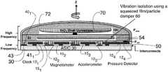
- FIG. 1 ais a side view schematic illustration of the monolithically formed INS showing sensor components sealed in individual environments and at specific required pressures, while FIG. 1 b is a cross section view thereof.
- FIGS. 2 a -2 jare across view (taken along line 2 - 2 shown in FIG. 1 b ) showing the steps used in a method described herein to form a slightly modified embodiment of the monolithically formed INS depicted by FIG. 1 a;
- FIG. 2 e 1is aside elevational view of the INS being formed at the step corresponding to FIG. 2 e.
- FIG. 1 aA schematic of the inertial navigation system (INS) is presented in FIG. 1 a , in which components of the INS are preferably formed monolithically and then wafer bonded to enclose each sensor (or device) 12 1 - 12 4 of the INS in individual environments with individual cavities 15 1 - 15 4 using respective caps 40 1 - 40 4 .
- the size of the composite unitis reduced and the alignment of the sensors (or devices) 12 1 - 12 4 within the system is also simplified since sensor alignment is achieved via lithographic wafer scale fabrication techniques and therefore post processing alignment can be eliminated.
- FIGS. 2 a -2 jthe corresponding fabrication process flow is shown below in FIGS. 2 a -2 j .
- the sensorsare typically sensors (such as compasses, pressure detectors, magnetometers and/or accelerometers), but devices (such as electronic clocks) are sometimes also used in an INS and can be embodied in the INS using the same construction techniques as used with the sensors, as is described below.
- FIG. 2 aInitially (see FIG. 2 a ) one begins with a quartz wafer 10 , a quartz or silicon handle wafer 20 , an Application Specific Integrated Circuit (ASIC) wafer 30 containing electronics and preferably as many silicon cap wafers 40 1 . . . 40 N as there are planned monolithic sensors 12 1 . . . 12 N to be formed from the quartz wafer 10 .
- the embodiment of FIGS. 2 a -2 jhas four sensors (or devices) three of which 12 1 . . . 12 3 are preferably totally encapsulated by an associated cap 40 1 . . . 40 3 in a hermitically sealed cavity 15 1 . . .
- 12 4(a pressure detector) is partially encapsulated by cap 40 4 and has an sealed cavity or pressure chamber 15 4 associated with it for containing a gas at a reference pressure P ref .
- the pressure detector 12 4detects a differential pressure across a diaphragm, one side of which is exposed to that reference pressure P ref and the other side of which is preferably exposed to ambient pressure via a channel 50 .
- the number and types of sensors and devicesmay be varied as needed to the use of any of them is optional.
- the quartz wafer 10is temporarily bonded to the quartz or silicon handle wafer 20 (the quartz wafer 10 is shown in dashed lines in FIG. 2 b ) using a temporary adhesive, for example wax, (not shown) or a temporary fusion bond, followed by thinning and patterning of the quartz wafer 10 to define individual quartz sensors and/or devices 12 from quartz wafer 10 which are thus temporarily adhered to the quartz or silicon handle wafer 20 by the aforementioned temporary adhesive or fusion bond (or other temporary bonding technique).
- the individual quartz sensors and/or devices 12 of FIG. 2 bare individually numbered 12 1 - 12 4 in the following figures. Four sensors and/or devices 12 are shown on FIG. 2 b , but the number of sensors and/or devices 12 formed from the quartz wafer 10 may be varied as needed to accommodate the number needed in the sensor suite to be monolithically encapsulated.
- the sensors and/or devices 12are bonded to the ASIC wafer 30 at bond regions 41 1 - 41 3 and at a ring bond 41 4 preferably using a thermo-compression bond under vacuum.
- the temporary quartz or silicon handle wafer 20is then preferably removed resulting in the structure depicted by FIG. 2 c .
- One of the sensorsis preferably a pressure sensor to sense ambient pressure and therefor an opening 52 in the bond ring 41 4 is provided to allow pressure equalization for the pressure sensor, which in this embodiment is sensor 12 4 . See FIG. 1 b.
- FIG. 2 dshows a cap wafer 40 with a single cavity 15 and an opening 44 therein (located between the cavity 15 and an end wall 51 ) positioned so that when this particular cap wafer 40 is applied to the structure depicted by FIG.
- the cavity 15 thereinwill cover and seal the left most sensor (or device) 12 1 shown in FIG. 2 c and leave the remaining sensors (or devices) 12 2 - 12 4 exposed through opening 44 .
- Cavities 15define the sealing environment (encapsulation) for typically a single sensor (or device) as each successive patterned cap wafer 40 is bonded into position on the ASIC wafer 30 .
- the openings or holes 44allow for a different environment when encapsulating of the other devices or sensors 12 .
- the first sensor (or device) 12 1(a quartz clock, for example, in the embodiment of FIG.
- the height of the bond regions 41 1 - 41 4 for the four sensors (or devices) 12 1 - 12 4 in this embodiment and the height of the peripheral bond region 43 for the four cap wafers 40 1 - 40 4 in this embodimentare exaggerated for ease of illustration.
- the peripheral bond region 43is also shown in FIG. 1 b by dashed lines.
- the peripheral bond region 43preferably completely encircles each of the four sensors or devices 12 1 - 12 4 except the last one ( 12 4 ) which is a preferably an ambient pressure detector and therefor needs a path 50 to ambient air. Therefore the pressure detector 12 4 is only partially encircled by the peripheral bond region 43 in that there is preferably a break or opening in bond region 43 labeled by numeral 54 .
- the end walls 51 of the four cap wafers 40 1 - 40 4each also preferably has an opening or notch 51 N therein to provide the path 50 to ambient air from sensor 12 4 through opening 52 and through the openings 54 and/or notches 51 N.
- the second sensor 12 2(a quartz magnetometer, for example, in the embodiment of FIG. 1 a ) is then encapsulated at a gas pressure P 2 in ambient gas G 2 with the second patterned cap wafer 40 2 at the peripheral bond 43 as shown in FIG. 2 f .
- This process with successive cap wafers 40(each with suitable cavities 15 and openings 44 defined therein) continues with the remaining sensors and cap wafers at their required environmental conditions being encapsulated preferably as shown by FIGS. 2 g and 2 h and bonded to layer 30 at, for example, bond the peripheral bond 43 .
- the encapsulated pressure(P 1 , P 2 , etc.) may be 0, i.e., a vacuum and the gases G 1 , and G 2 , etc., if used, are preferably nitrogen and/or helium.
- the same gas(or a common vacuum) be used in two different encapsulations. So each encapsulated environment may have its own unique gas type and pressure, but, if desired, neighboring sensors or devices can share a unique gas type and pressure if desired.
- each cap wafer 40not only encapsulates a single sensor (or device) 12 with a desired gas at a desired pressure, but also re-encapsulates the previously encapsulated sensors (or devices) 12 .
- each successive cap wafer 40may be formed instead to encapsulate only its associated sensor without also encapsulating any previous encapsulations as shown in FIG. 1 a .
- various combinations of these two encapsulation techniqueswill suggest themselves to those skilled in the art.
- the bonds 41 1 - 41 4 and 43are preferably formed as a thermo-compression metal bond but other bond techniques could alternatively be used especially if the bonds need to be made at lower than usual temperatures for thermo-compression bonding due to, for example, a temperature sensitivity of one or more of the sensors.
- the stoichiometry of the bonds 43 for each of the cap wafers 40is preferably selected to achieve a hermetic seal of the encapsulated sensors 12 1 - 12 3 within cavities 15 .
- the fourth device 12 4 in this embodimentis preferably a pressure sensor which has a diaphragm 56 (see FIG. 2 g ) which is sealed around its perimeter by a perimeter seal 55 from above to define the cavity or chamber 15 4 which preferably formed at the reference pressure of P ref .
- a air path 50(see also FIG. 2 el ) to ambient in the form of the missing segment 52 of the bond metal ring 41 4 and the missing portion 54 in the peripheral bond 43 in combination with opening(s) and/or notch(es) 51 N allows equalization of the pressure under the diaphragm 56 with the ambient pressure to be measured via the air path 50 .
- the pressure sensor 12 4 of this embodimentmeasures a differential pressure difference across diaphragm 56 .
- the pressureis well defined (at a reference pressure P ref ) by the capping process of cap wafer 40 4 under a controlled environment (gas and pressure) at seals 54 .
- the damping unit 60may be used as the final cap (see FIG. 1 a ).
- the final cap wafer 40 4 in the embodiment of FIG. 2 hutilizes a seal 54 at the edge of the cavity 15 4 thereby locking in that controlled environment between the diaphragm 56 and the cap.
- the gap or opening 52 in the seal ring 41 4allows pressure to equalize to ambient pressure (via passage 50 ), which is the pressure to be measured.
- Vibration isolationis desirable for many sensors and therefore a silicon wafer containing a vibration damping unit 60 is preferably bonded (see FIG. 2 i ) to the topmost cap 40 of the capped wafer stack shown in FIG. 2 h .
- the vibration damping unit 60may utilize a squeezed film or particles as the damping agent.
- the final componentis preferably a gyroscope 70 which is bonded to the top of the vibration damping unit 60 (see FIG. 2 j ) to complete the encapsulation of the inertial navigation system.
- the vibration damping unit 60is preferably bonded to the composite unit depicted in FIG. 2 h providing a vibration-damped surface for receiving the gyroscope 70 .
- the gyroscope 70is mounted on the vibration damping unit 60 .
- the vibration damping unit 60may be fabricated using standard MEMS fabrications techniques.
- Preferred materials for the composite unitinclude semiconductors (silicon, etc.), dielectrics (silicon dioxide, silicon nitride, etc.), metals (aluminum, gold, titanium, etc) and polymers (polyamide, etc.).
- the vibration damping unit 60in some embodiments may be located under the ASIC wafer 30 (as viewed in FIG. 1 a ) instead of (or in addition to) on top of the encapsulated sensors 12 if none of the sensors is an accelerometer, for example.
- the gyroscope 70 , the damper 60 and the sensors 12may be all enclosed within a rounded shell 72 as depicted by FIG. 1 a if desired.
- the shell 72may assume some other geometric shape (square, rectangular, etc.).
- sensor or device 12 1may serve as a resonator for a clock, while sensor or device 12 2 may be magnetometer while sensor or device 12 3 may be an accelerometer in order to form an INS as mentioned above.
- the sensors and devices 12 1 - 12 4may perform other or additional tasks if desired.
- This methodmay utilize quartz processing techniques described in U.S. Pat. No. 7,237,315 to make quartz based sensors 12 .
Landscapes
- Engineering & Computer Science (AREA)
- Microelectronics & Electronic Packaging (AREA)
- Computer Hardware Design (AREA)
- Manufacturing & Machinery (AREA)
- Physics & Mathematics (AREA)
- General Physics & Mathematics (AREA)
- Radar, Positioning & Navigation (AREA)
- Remote Sensing (AREA)
- Chemical & Material Sciences (AREA)
- Analytical Chemistry (AREA)
- Pressure Sensors (AREA)
Abstract
Description
Claims (25)
Priority Applications (1)
| Application Number | Priority Date | Filing Date | Title |
|---|---|---|---|
| US16/376,970US11117800B2 (en) | 2014-08-11 | 2019-04-05 | Method and apparatus for the monolithic encapsulation of a micro-scale inertial navigation sensor suite |
Applications Claiming Priority (2)
| Application Number | Priority Date | Filing Date | Title |
|---|---|---|---|
| US14/456,808US10308505B1 (en) | 2014-08-11 | 2014-08-11 | Method and apparatus for the monolithic encapsulation of a micro-scale inertial navigation sensor suite |
| US16/376,970US11117800B2 (en) | 2014-08-11 | 2019-04-05 | Method and apparatus for the monolithic encapsulation of a micro-scale inertial navigation sensor suite |
Related Parent Applications (1)
| Application Number | Title | Priority Date | Filing Date |
|---|---|---|---|
| US14/456,808DivisionUS10308505B1 (en) | 2014-08-11 | 2014-08-11 | Method and apparatus for the monolithic encapsulation of a micro-scale inertial navigation sensor suite |
Publications (2)
| Publication Number | Publication Date |
|---|---|
| US20190315621A1 US20190315621A1 (en) | 2019-10-17 |
| US11117800B2true US11117800B2 (en) | 2021-09-14 |
Family
ID=66673466
Family Applications (2)
| Application Number | Title | Priority Date | Filing Date |
|---|---|---|---|
| US14/456,808Active2034-09-04US10308505B1 (en) | 2014-08-11 | 2014-08-11 | Method and apparatus for the monolithic encapsulation of a micro-scale inertial navigation sensor suite |
| US16/376,970ActiveUS11117800B2 (en) | 2014-08-11 | 2019-04-05 | Method and apparatus for the monolithic encapsulation of a micro-scale inertial navigation sensor suite |
Family Applications Before (1)
| Application Number | Title | Priority Date | Filing Date |
|---|---|---|---|
| US14/456,808Active2034-09-04US10308505B1 (en) | 2014-08-11 | 2014-08-11 | Method and apparatus for the monolithic encapsulation of a micro-scale inertial navigation sensor suite |
Country Status (1)
| Country | Link |
|---|---|
| US (2) | US10308505B1 (en) |
Families Citing this family (8)
| Publication number | Priority date | Publication date | Assignee | Title |
|---|---|---|---|---|
| US10308505B1 (en) | 2014-08-11 | 2019-06-04 | Hrl Laboratories, Llc | Method and apparatus for the monolithic encapsulation of a micro-scale inertial navigation sensor suite |
| EP3501149B1 (en)* | 2016-08-31 | 2020-05-13 | Huawei Technologies Duesseldorf GmbH | Filtered multi-carrier communications |
| US11239823B1 (en) | 2017-06-16 | 2022-02-01 | Hrl Laboratories, Llc | Quartz MEMS piezoelectric resonator for chipscale RF antennae |
| US11101786B1 (en) | 2017-06-20 | 2021-08-24 | Hrl Laboratories, Llc | HF-VHF quartz MEMS resonator |
| US10921360B2 (en)* | 2018-02-09 | 2021-02-16 | Hrl Laboratories, Llc | Dual magnetic and electric field quartz sensor |
| US10819276B1 (en) | 2018-05-31 | 2020-10-27 | Hrl Laboratories, Llc | Broadband integrated RF magnetic antenna |
| US11563420B1 (en) | 2019-03-29 | 2023-01-24 | Hrl Laboratories, Llc | Femto-tesla MEMS RF antenna with integrated flux concentrator |
| US11988727B1 (en) | 2019-07-31 | 2024-05-21 | Hrl Laboratories, Llc | Magnetostrictive MEMS magnetic gradiometer |
Citations (222)
| Publication number | Priority date | Publication date | Assignee | Title |
|---|---|---|---|---|
| US392650A (en) | 1888-11-13 | watrous | ||
| US2487165A (en) | 1946-10-10 | 1949-11-08 | August E Miller | Crystal electrode |
| US3390287A (en) | 1964-12-10 | 1968-06-25 | Kistler Instrumente Ag | Piezo-electric building units |
| US3766616A (en) | 1972-03-22 | 1973-10-23 | Statek Corp | Microresonator packaging and tuning |
| JPS5791017A (en) | 1980-11-27 | 1982-06-07 | Seiko Instr & Electronics Ltd | Gt-cut quartz oscillator |
| US4364016A (en) | 1980-11-03 | 1982-12-14 | Sperry Corporation | Method for post fabrication frequency trimming of surface acoustic wave devices |
| WO1984000082A1 (en) | 1982-06-14 | 1984-01-05 | Gte Prod Corp | Trimming of piezoelectric components |
| US4426769A (en) | 1981-08-14 | 1984-01-24 | Amp Incorporated | Moisture getter for integrated circuit packages |
| US4442574A (en) | 1982-07-26 | 1984-04-17 | General Electric Company | Frequency trimming of saw resonators |
| US4618262A (en) | 1984-04-13 | 1986-10-21 | Applied Materials, Inc. | Laser interferometer system and method for monitoring and controlling IC processing |
| US4655081A (en) | 1984-02-22 | 1987-04-07 | National Research Development Corporation | Gyroscopic devices |
| JPS6232678B2 (en) | 1981-03-30 | 1987-07-16 | Oki Electric Ind Co Ltd | |
| JPH01129517A (en) | 1987-11-13 | 1989-05-22 | Fujitsu Ltd | Manufacture of surface wave resonance element |
| US4870313A (en) | 1985-04-11 | 1989-09-26 | Toyo Communication Equipment Co., Ltd. | Piezoelectric resonators for overtone oscillations |
| US4898031A (en) | 1987-07-24 | 1990-02-06 | Yazaki Corporation | Vibrational angular velocity sensor |
| US4944836A (en) | 1985-10-28 | 1990-07-31 | International Business Machines Corporation | Chem-mech polishing method for producing coplanar metal/insulator films on a substrate |
| EP0461761A1 (en) | 1990-05-18 | 1991-12-18 | British Aerospace Public Limited Company | Inertial sensors |
| JPH04322507A (en) | 1991-04-22 | 1992-11-12 | Matsushita Electric Ind Co Ltd | How to process crystal resonators |
| EP0531985A1 (en) | 1991-09-12 | 1993-03-17 | Matsushita Electric Industrial Co., Ltd. | Electro-acoustic hybrid integrated circuit and manufacturing method thereof |
| US5203208A (en) | 1991-04-29 | 1993-04-20 | The Charles Stark Draper Laboratory | Symmetrical micromechanical gyroscope |
| JPH05286142A (en) | 1992-04-13 | 1993-11-02 | Fujitsu Ltd | Inkjet head and manufacturing method thereof |
| US5260596A (en) | 1991-04-08 | 1993-11-09 | Motorola, Inc. | Monolithic circuit with integrated bulk structure resonator |
| JPH06318533A (en) | 1993-02-03 | 1994-11-15 | Tama Electric Co Ltd | Electronic component |
| US5421312A (en) | 1990-11-03 | 1995-06-06 | Dawson Royalties Limited | Electrical circuit |
| US5480747A (en) | 1994-11-21 | 1996-01-02 | Sematech, Inc. | Attenuated phase shifting mask with buried absorbers |
| DE4442033A1 (en) | 1994-11-25 | 1996-05-30 | Bosch Gmbh Robert | Yaw rate sensor |
| US5530408A (en) | 1995-05-25 | 1996-06-25 | The United States Of America As Represented By The Secretary Of The Army | Method of making an oven controlled crystal oscillator the frequency of which remains ultrastable under temperature variations |
| US5552016A (en) | 1993-04-28 | 1996-09-03 | Applied Materials, Inc. | Method and apparatus for etchback endpoint detection |
| US5578976A (en) | 1995-06-22 | 1996-11-26 | Rockwell International Corporation | Micro electromechanical RF switch |
| WO1996038710A1 (en) | 1995-05-31 | 1996-12-05 | Litef Gmbh | Micromechanical rotation speed sensor |
| JPH08330878A (en) | 1995-06-02 | 1996-12-13 | Matsushita Electric Ind Co Ltd | Oscillator manufacturing method |
| US5589724A (en) | 1993-01-25 | 1996-12-31 | Matsushita Electric Industrial Co., Ltd. | Piezoelectric device and a package |
| US5605490A (en) | 1994-09-26 | 1997-02-25 | The United States Of America As Represented By The Secretary Of The Army | Method of polishing langasite |
| US5644139A (en) | 1995-03-02 | 1997-07-01 | Allen; Ross R. | Navigation technique for detecting movement of navigation sensors relative to an object |
| US5646346A (en) | 1994-11-10 | 1997-07-08 | Okada; Kazuhiro | Multi-axial angular velocity sensor |
| US5648849A (en) | 1994-04-05 | 1997-07-15 | Sofie | Method of and device for in situ real time quantification of the morphology and thickness of a localized area of a surface layer of a thin layer structure during treatment of the latter |
| US5658418A (en) | 1995-03-31 | 1997-08-19 | International Business Machines Corporation | Apparatus for monitoring the dry etching of a dielectric film to a given thickness in an integrated circuit |
| US5665915A (en) | 1992-03-25 | 1997-09-09 | Fuji Electric Co., Ltd. | Semiconductor capacitive acceleration sensor |
| US5666706A (en) | 1993-06-10 | 1997-09-16 | Matsushita Electric Industrial Co., Ltd. | Method of manufacturing a piezoelectric acoustic wave device |
| US5668057A (en) | 1991-03-13 | 1997-09-16 | Matsushita Electric Industrial Co., Ltd. | Methods of manufacture for electronic components having high-frequency elements |
| JPH09247025A (en) | 1996-03-11 | 1997-09-19 | Murata Mfg Co Ltd | Antenna system |
| US5728936A (en) | 1995-08-16 | 1998-03-17 | Robert Bosch Gmbh | Rotary speed sensor |
| WO1998015799A1 (en) | 1996-10-07 | 1998-04-16 | HAHN-SCHICKARD-GESELLSCHAFT FÜR ANGEWANDTE FORSCHUNG E.V. Wilhelm-Schickard-Strasse 10 | Rotation rate sensor with uncoupled mutually perpendicular primary and secondary oscillations |
| US5783749A (en) | 1995-12-07 | 1998-07-21 | Electronics And Telecommunications Research Institute | Vibrating disk type micro-gyroscope |
| DE19719601A1 (en) | 1997-05-09 | 1998-11-12 | Bosch Gmbh Robert | Acceleration sensor with spring-mounted seismic mass |
| US5894090A (en) | 1996-05-31 | 1999-04-13 | California Institute Of Technology | Silicon bulk micromachined, symmetric, degenerate vibratorygyroscope, accelerometer and sensor and method for using the same |
| US5905202A (en) | 1995-09-01 | 1999-05-18 | Hughes Electronics Corporation | Tunneling rotation sensor |
| US5920012A (en) | 1998-06-16 | 1999-07-06 | Boeing North American | Micromechanical inertial sensor |
| US5928532A (en) | 1996-11-11 | 1999-07-27 | Tokyo Electron Limited | Method of detecting end point of plasma processing and apparatus for the same |
| US5942445A (en) | 1996-03-25 | 1999-08-24 | Shin-Etsu Handotai Co., Ltd. | Method of manufacturing semiconductor wafers |
| US5981392A (en) | 1996-03-28 | 1999-11-09 | Shin-Etsu Handotai Co., Ltd. | Method of manufacturing semiconductor monocrystalline mirror-surface wafers which includes a gas phase etching process, and semiconductor monocrystalline mirror-surface wafers manufactured by the method |
| US6009751A (en) | 1998-10-27 | 2000-01-04 | Ljung; Bo Hans Gunnar | Coriolis gyro sensor |
| EP0971208A2 (en) | 1998-07-10 | 2000-01-12 | Murata Manufacturing Co., Ltd. | Angular velocity sensor |
| US6044705A (en) | 1993-10-18 | 2000-04-04 | Xros, Inc. | Micromachined members coupled for relative rotation by torsion bars |
| US6049702A (en) | 1997-12-04 | 2000-04-11 | Rockwell Science Center, Llc | Integrated passive transceiver section |
| US6081334A (en) | 1998-04-17 | 2000-06-27 | Applied Materials, Inc | Endpoint detection for semiconductor processes |
| US6089088A (en) | 1997-11-07 | 2000-07-18 | Commissariat A L'energie Atomique | Vibrating microgyrometer |
| US6094985A (en) | 1996-11-22 | 2000-08-01 | Siemens Aktiengesellschaft | Rotation rate sensor |
| US6114801A (en) | 1997-04-14 | 2000-09-05 | Toyo Communication Equipment Co., Ltd. | At-cut crystal resonator |
| US6145380A (en) | 1997-12-18 | 2000-11-14 | Alliedsignal | Silicon micro-machined accelerometer using integrated electrical and mechanical packaging |
| WO2000068640A2 (en) | 1999-04-21 | 2000-11-16 | The Regents Of The University Of California | Micro-machined angle-measuring gyroscope |
| US6151964A (en) | 1998-05-25 | 2000-11-28 | Citizen Watch Co., Ltd. | Angular velocity sensing device |
| EP1055908A1 (en) | 1999-05-27 | 2000-11-29 | Delphi Technologies, Inc. | Angular rate sensor |
| US6155115A (en) | 1991-01-02 | 2000-12-05 | Ljung; Per | Vibratory angular rate sensor |
| US6164134A (en) | 1999-01-29 | 2000-12-26 | Hughes Electronics Corporation | Balanced vibratory gyroscope and amplitude control for same |
| US6182352B1 (en) | 1997-06-02 | 2001-02-06 | Avery Dennison Corporation | Method of manufacturing an EAS marker |
| US6196059B1 (en) | 1997-08-11 | 2001-03-06 | Fraunhofer Gesellschaft Zur Forderung Der Angewandten Forschung E.V. | Piezoelectric resonator, process for the fabrication thereof including its use as a sensor element for the determination of the concentration of a substance contained in a liquid and/or for the determination of the physical properties of the liquid |
| US6204737B1 (en) | 1998-06-02 | 2001-03-20 | Nokia Mobile Phones, Ltd | Piezoelectric resonator structures with a bending element performing a voltage controlled switching function |
| US6207008B1 (en) | 1997-12-15 | 2001-03-27 | Ricoh Company, Ltd. | Dry etching endpoint detection system |
| US6236145B1 (en) | 2000-02-29 | 2001-05-22 | Cts Corporation | High thermal resistivity crystal resonator support structure and oscillator package |
| WO2001044823A1 (en) | 1999-12-16 | 2001-06-21 | Robert Bosch Gmbh | Micromechanical spring structure, especially for a rotational speed sensor |
| US6250157B1 (en) | 1998-06-22 | 2001-06-26 | Aisin Seiki Kabushiki Kaisha | Angular rate sensor |
| US6263552B1 (en) | 1995-12-28 | 2001-07-24 | Ngk Insulators, Ltd. | Method of producing piezoelectric/electrostrictive film-type element |
| US6282958B1 (en) | 1998-08-11 | 2001-09-04 | Bae Systems Plc | Angular rate sensor |
| US6289733B1 (en) | 1999-05-12 | 2001-09-18 | Hughes Electronics Corporation | Planar vibratory gyroscopes |
| US6297064B1 (en) | 1998-02-03 | 2001-10-02 | Tokyo Electron Yamanashi Limited | End point detecting method for semiconductor plasma processing |
| WO2001074708A2 (en) | 2000-04-05 | 2001-10-11 | Interuniversitair Microelektronica Centrum (Imec) | Method for depositing polycrystalline sige suitable for micromachining and devices obtained thereof |
| KR20010110428A (en) | 1999-02-01 | 2001-12-13 | 비르 에이/에스 | A surface plasmon resonance sensor |
| WO2002012873A2 (en) | 2000-08-08 | 2002-02-14 | Smithkline Beecham P.L.C. | Quartz crystal microbalance |
| US6367326B1 (en) | 1996-07-10 | 2002-04-09 | Wacoh Corporation | Angular velocity sensor |
| US6367786B1 (en) | 1999-06-07 | 2002-04-09 | California Institute Of Technology | Micromachined double resonator |
| US20020066317A1 (en) | 2000-12-06 | 2002-06-06 | Gang Lin | Micro yaw rate sensors |
| US20020072246A1 (en) | 2000-12-11 | 2002-06-13 | Samsung Electronics Co., Ltd. | Method of forming a spin-on-glass insulation layer |
| US20020074947A1 (en) | 2000-09-01 | 2002-06-20 | Takeo Tsukamoto | Electron-emitting device, electron-emitting apparatus, image display apparatus, and light-emitting apparatus |
| US6413682B1 (en) | 1999-05-21 | 2002-07-02 | Shin-Etsu Chemical Co., Ltd. | Synthetic quartz glass substrate for photomask and making method |
| US6417925B1 (en) | 1999-08-26 | 2002-07-09 | Fuji Photo Film Co., Ltd. | Surface plasmon sensor for analyzing liquid sample or humid atmosphere |
| US6424418B2 (en) | 1998-05-29 | 2002-07-23 | Canon Kabushiki Kaisha | Surface plasmon resonance sensor apparatus using surface emitting laser |
| US6426296B1 (en) | 2000-09-08 | 2002-07-30 | The United States Of America As Represented By The Administrator Of The National Aeronautics And Space Administration | Method and apparatus for obtaining a precision thickness in semiconductor and other wafers |
| US6432824B2 (en) | 2000-02-25 | 2002-08-13 | Speedfam Co., Ltd. | Method for manufacturing a semiconductor wafer |
| US6481284B2 (en) | 1997-09-02 | 2002-11-19 | Analog Devices, Inc. | Micromachined devices with anti-levitation devices |
| US6492195B2 (en) | 1999-12-24 | 2002-12-10 | Hitachi, Ltd. | Method of thinning a semiconductor substrate using a perforated support substrate |
| US20030003608A1 (en) | 2001-03-21 | 2003-01-02 | Tsunetoshi Arikado | Semiconductor wafer with ID mark, equipment for and method of manufacturing semiconductor device from them |
| US20030010123A1 (en) | 2000-01-13 | 2003-01-16 | Malvern Alan R | Accelerometer |
| US6515278B2 (en) | 1999-08-05 | 2003-02-04 | Microvision, Inc. | Frequency tunable resonant scanner and method of making |
| US6514767B1 (en) | 1999-10-06 | 2003-02-04 | Surromed, Inc. | Surface enhanced spectroscopy-active composite nanoparticles |
| US6513380B2 (en) | 2001-06-19 | 2003-02-04 | Microsensors, Inc. | MEMS sensor with single central anchor and motion-limiting connection geometry |
| US20030029238A1 (en) | 2001-08-10 | 2003-02-13 | The Boeing Company | Isolated resonator gyroscope |
| US6584845B1 (en) | 1999-02-10 | 2003-07-01 | California Institute Of Technology | Inertial sensor and method of use |
| US6614529B1 (en) | 1992-12-28 | 2003-09-02 | Applied Materials, Inc. | In-situ real-time monitoring technique and apparatus for endpoint detection of thin films during chemical/mechanical polishing planarization |
| US6621158B2 (en) | 1995-06-06 | 2003-09-16 | Analog Devices, Inc. | Package for sealing an integrated circuit die |
| US6628177B2 (en) | 2000-08-24 | 2003-09-30 | The Regents Of The University Of Michigan | Micromechanical resonator device and micromechanical device utilizing same |
| US6627067B1 (en) | 1999-06-22 | 2003-09-30 | President And Fellows Of Harvard College | Molecular and atomic scale evaluation of biopolymers |
| US20030196490A1 (en) | 2002-04-17 | 2003-10-23 | Donato Cardarelli | MEMS-integrated inertial measurement units on a common substrate |
| US20030205948A1 (en) | 2002-05-03 | 2003-11-06 | Asia Pacific Microsystems, Inc. | Film bulk acoustic device with integrated tunable and trimmable device |
| JP2003318685A (en) | 2002-04-22 | 2003-11-07 | Herutsu Kk | Manufacturing method of quartz resonator |
| US6651027B2 (en) | 1999-09-20 | 2003-11-18 | American Gnc Corporation | Processing method for motion measurement |
| US6662656B2 (en) | 2000-02-15 | 2003-12-16 | Sagem S.A. | Gyroscopic sensor |
| US6686807B1 (en) | 1999-11-02 | 2004-02-03 | Eta Sa Fabriques D'ebauches | Time base comprising an integrated micromechanical ring resonator |
| US6710681B2 (en) | 2001-07-13 | 2004-03-23 | Agilent Technologies, Inc. | Thin film bulk acoustic resonator (FBAR) and inductor on a monolithic substrate and method of fabricating the same |
| US20040055380A1 (en) | 2002-08-12 | 2004-03-25 | Shcheglov Kirill V. | Isolated planar gyroscope with internal radial sensing and actuation |
| US6715352B2 (en) | 2001-06-26 | 2004-04-06 | Microsensors, Inc. | Method of designing a flexure system for tuning the modal response of a decoupled micromachined gyroscope and a gyroscoped designed according to the method |
| US20040065864A1 (en) | 2000-12-20 | 2004-04-08 | Kristina Vogt | Acidic polishing slurry for the chemical-mechanical polishing of SiO2 isolation layers |
| US6744335B2 (en) | 2000-02-16 | 2004-06-01 | Nokia Mobile Phones Ltd. | Micromechanical tunable capacitor and an integrated tunable resonator |
| US6750728B2 (en) | 2002-03-28 | 2004-06-15 | Humo Laboratory, Ltd. | Quartz oscillator and method for manufacturing the same |
| US6756304B1 (en) | 1999-07-30 | 2004-06-29 | Thales Avionics S.A. | Method for producing via-connections in a substrate and substrate equipped with same |
| US6768396B2 (en) | 1999-12-22 | 2004-07-27 | Koninklijke Philips Electronics N.V. | Filter arrangement |
| US6796179B2 (en) | 2002-05-17 | 2004-09-28 | California Institute Of Technology | Split-resonator integrated-post MEMS gyroscope |
| US20040189311A1 (en) | 2002-12-26 | 2004-09-30 | Glezer Eli N. | Assay cartridges and methods of using the same |
| US6806557B2 (en) | 2002-09-30 | 2004-10-19 | Motorola, Inc. | Hermetically sealed microdevices having a single crystalline silicon getter for maintaining vacuum |
| US20040211052A1 (en) | 2002-04-30 | 2004-10-28 | Kubena Randall L. | Quartz-based nanoresonators and method of fabricating same |
| US20040219700A1 (en)* | 2001-01-10 | 2004-11-04 | Kia Silverbrook | Method of manufacturing a light emitting semiconductor package |
| US6815228B2 (en) | 2000-06-20 | 2004-11-09 | Hitachi, Ltd. | Film thickness measuring method of member to be processed using emission spectroscopy and processing method of the member using the measuring method |
| US20040239341A1 (en) | 2003-03-19 | 2004-12-02 | California Institute Of Technology | Parylene capacitive accelerometer utilizing electrical fringing field sensing and method of making |
| US20050034822A1 (en) | 2003-04-22 | 2005-02-17 | Samsung Electronics Co., Ltd. | Method for fabricating cantilevered type film bulk acoustic resonator and film bulk acoustic resonator fabricated by the same |
| US6862398B2 (en) | 2001-03-30 | 2005-03-01 | Texas Instruments Incorporated | System for directed molecular interaction in surface plasmon resonance analysis |
| US20050062368A1 (en) | 2003-08-19 | 2005-03-24 | Seiko Epson Corporation | Tuning-fork type piezo-oscillator piece and mounting method thereof |
| US6883374B2 (en) | 2001-09-14 | 2005-04-26 | Bae Systems Plc | Vibratory gyroscopic rate sensor |
| US20050093659A1 (en) | 2003-10-30 | 2005-05-05 | Larson John D.Iii | Film acoustically-coupled transformer with increased common mode rejection |
| US6915215B2 (en) | 2002-06-25 | 2005-07-05 | The Boeing Company | Integrated low power digital gyro control electronics |
| JP2005180921A (en) | 2002-04-03 | 2005-07-07 | Japan Science & Technology Agency | Biosensor chip surface carrying polyethylene glycol modified nanoparticles |
| US20050156309A1 (en) | 1999-03-19 | 2005-07-21 | Tetsuo Fujii | Semiconductor sensor |
| US20050172714A1 (en) | 2002-08-12 | 2005-08-11 | California Institute Of Technology | Isolated planar mesogyroscope |
| US6933164B2 (en) | 2001-08-30 | 2005-08-23 | Hrl Laboratories, Llc | Method of fabrication of a micro-channel based integrated sensor for chemical and biological materials |
| US6943484B2 (en) | 2001-12-06 | 2005-09-13 | University Of Pittsburgh | Tunable piezoelectric micro-mechanical resonator |
| US20050260792A1 (en) | 2000-12-07 | 2005-11-24 | Patel Satyadev R | Methods for depositing, releasing and packaging micro-electromechanical devices on wafer substrates |
| WO2005121769A1 (en) | 2004-06-12 | 2005-12-22 | Akubio Limited | Analytical apparatus with array of sensors and calibrating element |
| US6985051B2 (en) | 2002-12-17 | 2006-01-10 | The Regents Of The University Of Michigan | Micromechanical resonator device and method of making a micromechanical device |
| US20060016065A1 (en) | 2000-07-17 | 2006-01-26 | Yoshiaki Nagaura | Piezoelectric device and acousto-electric transducer and method for manufacturing the same |
| US20060022556A1 (en) | 2004-07-29 | 2006-02-02 | Bail David L | Quartz resonator package having a housing with thermally coupled internal heating element |
| WO2006010206A1 (en) | 2004-07-29 | 2006-02-02 | Mnt Innovations Pty Ltd | Biological saw sensor |
| US20060055479A1 (en) | 2004-09-14 | 2006-03-16 | Masayoshi Okazaki | Surface mount crystal oscillator |
| US20060066419A1 (en) | 2004-09-28 | 2006-03-30 | Fujitsu Media Devices Limited And Fujitsu Limited | Duplexer |
| US7057331B2 (en) | 2003-03-13 | 2006-06-06 | Seiko Epson Corporation | Piezoelectric oscillator, portable telephone unit using piezoelectric oscillator, and electronic equipment using piezoelectric oscillator |
| US20060139121A1 (en) | 2003-02-22 | 2006-06-29 | Jaemyoung Jhung | Fbar band pass filter, duplexer having the filter and methods for manufacturing the same |
| US20060144142A1 (en)* | 2005-01-06 | 2006-07-06 | Gogoi Bishnu P | Multiple microelectromechanical (MEM) devices formed on a single substrate and sealed at different pressures and method therefor |
| US20060197619A1 (en) | 2004-07-12 | 2006-09-07 | Epson Toyocom Corporation | Piezoelectric oscillator and manufacturing method thereof |
| US20060213266A1 (en) | 2005-03-22 | 2006-09-28 | Honeywell International Inc. | Use of electrodes to cancel lift effects in inertial sensors |
| WO2006103439A2 (en) | 2005-04-01 | 2006-10-05 | Akubio Limited | Cartridge for a fluid sample analyser |
| US7118657B2 (en) | 1999-06-22 | 2006-10-10 | President And Fellows Of Harvard College | Pulsed ion beam control of solid state features |
| US20060252906A1 (en) | 2003-02-20 | 2006-11-09 | Godschalx James P | Method of synthesis of polyarylenes and the polyarylenes made by such method |
| US7152290B2 (en) | 2002-03-18 | 2006-12-26 | Seiko Epson Corporation | Methods of manufacturing a piezoelectric actuator and a liquid jetting head |
| JP2006352487A (en) | 2005-06-15 | 2006-12-28 | Epson Toyocom Corp | Piezoelectric oscillator manufacturing method and piezoelectric oscillator |
| US20060290449A1 (en) | 2005-06-02 | 2006-12-28 | The Regents Of The University Of California | Contour-mode piezoelectric micromechanical resonators |
| US20070017287A1 (en) | 2005-07-20 | 2007-01-25 | The Boeing Company | Disc resonator gyroscopes |
| US20070034005A1 (en) | 2005-08-15 | 2007-02-15 | Cenk Acar | Robust micromachined gyroscopes with two degrees of freedom sense-mode oscillator |
| US7211933B2 (en) | 2003-09-19 | 2007-05-01 | Kabushiki Kaisha Toshiba | Voltage controlled oscillator |
| US7224245B2 (en) | 2003-12-22 | 2007-05-29 | Samsung Electronics Co., Ltd. | Duplexer fabricated with monolithic FBAR and isolation part and a method thereof |
| US7232700B1 (en) | 2004-12-08 | 2007-06-19 | Hrl Laboratories, Llc | Integrated all-Si capacitive microgyro with vertical differential sense and control and process for preparing an integrated all-Si capacitive microgyro with vertical differential sense |
| US7234214B2 (en) | 2003-02-25 | 2007-06-26 | Palo Alto Research Center Incorporated | Methods for making thick film elements |
| US20070161210A1 (en)* | 2006-01-12 | 2007-07-12 | Shih-Feng Shao | Method for wafer level packaging and fabricating cap structures |
| US20070220971A1 (en) | 2006-03-27 | 2007-09-27 | Georgia Tech Research Corporation | Capacitive bulk acoustic wave disk gyroscopes |
| US7281425B2 (en) | 2005-05-31 | 2007-10-16 | Innalabs Technologies, Inc. | Coriolis force gyroscope with high sensitivity |
| US20070240508A1 (en) | 2006-04-18 | 2007-10-18 | Watson William S | Vibrating inertial rate sensor utilizing skewed drive or sense elements |
| US7295088B2 (en) | 2004-01-21 | 2007-11-13 | The Regents Of The University Of Michigan | High-Q micromechanical resonator devices and filters utilizing same |
| US7317354B2 (en) | 2005-06-16 | 2008-01-08 | Via Technologies, Inc. | Inductor |
| US20080034575A1 (en) | 2006-08-09 | 2008-02-14 | Chang David T | Large area integration of quartz resonators with electronics |
| US20080074661A1 (en) | 2006-09-21 | 2008-03-27 | Jingwu Zhang | Online analyte detection by surface enhanced Raman scattering (SERS) |
| US20080096313A1 (en) | 2000-12-07 | 2008-04-24 | Texas Instruments Incorporated | Methods for Depositing, Releasing and Packaging Micro-Electromechanical Devices on Wafer Substrates |
| US20080148846A1 (en) | 2006-12-22 | 2008-06-26 | The Boeing Company | Vibratory gyroscope with parasitic mode damping |
| US7404325B2 (en) | 2003-12-19 | 2008-07-29 | Commissariat A L'energie Atomique | Micro-machined vibrating structure and associated micro-gyroscope |
| US7446628B2 (en) | 2004-12-09 | 2008-11-04 | Wispry, Inc. | Pole-zero elements and related systems and methods |
| US7459992B2 (en) | 2005-05-25 | 2008-12-02 | Fujitsu Media Devices Limited | Acoustic wave filter and acoustic wave duplexer |
| US7479846B2 (en) | 2004-11-02 | 2009-01-20 | Fujitsu Media Devices Limited | Duplexer |
| US20090146527A1 (en) | 2007-12-07 | 2009-06-11 | Electronics And Telecommunications Research Institute | Piezoelectric microspeaker using microelectromechanical systems and method of manufacturing the same |
| US7551054B2 (en) | 2004-11-30 | 2009-06-23 | Fujitsu Limited | Electronic device and method of manufacturing the same |
| US7557493B2 (en) | 2006-02-10 | 2009-07-07 | Murata Manufacturing Co., Ltd. | Vibrator module |
| US7564177B2 (en) | 2006-12-26 | 2009-07-21 | Nihon Dempa Kogyo Co., Ltd. | Crystal unit having stacked structure |
| US7579748B2 (en) | 2006-08-18 | 2009-08-25 | Epson Toyocom Corporation | Piezoelectric device and method for manufacturing thereof |
| JP4322507B2 (en) | 2003-01-15 | 2009-09-02 | 株式会社デルタツーリング | Magnetizer |
| US20100000324A1 (en) | 2007-05-30 | 2010-01-07 | Rohm Co., Ltd. | Acceleration sensor and method of fabricating it |
| US20100020311A1 (en) | 2007-06-14 | 2010-01-28 | Hrl Laboratories, Llc | Integrated quartz biological sensor and method |
| US20100024546A1 (en) | 2007-07-31 | 2010-02-04 | The Boeing Company | Disc resonator integral inertial measurement unit |
| US7663196B2 (en) | 2007-02-09 | 2010-02-16 | Freescale Semiconductor, Inc. | Integrated passive device and method of fabrication |
| US7671427B2 (en) | 2003-05-22 | 2010-03-02 | Samsung Electronics Co., Ltd. | Method of manufacturing film bulk acoustic resonator using internal stress of metallic film and resonator manufactured thereby |
| US7675224B2 (en) | 2005-04-27 | 2010-03-09 | Seiko Epson Corporation | Piezoelectric vibrating reed and piezoelectric device |
| US20100148803A1 (en) | 2005-05-31 | 2010-06-17 | Ngk Insulators, Ltd. | Passage detection apparatus of object |
| US7757393B2 (en) | 2005-06-03 | 2010-07-20 | Georgia Tech Research Corporation | Capacitive microaccelerometers and fabrication methods |
| US7791431B2 (en) | 2006-12-04 | 2010-09-07 | Electronics And Telecommunications Research Institute | 3-port orthogonal mode transducer and receiver and receiving method using the same |
| US7802356B1 (en) | 2008-02-21 | 2010-09-28 | Hrl Laboratories, Llc | Method of fabricating an ultra thin quartz resonator component |
| US7830074B2 (en) | 2006-08-08 | 2010-11-09 | Hrl Laboratories, Llc | Integrated quartz oscillator on an active electronic substrate |
| US20100314969A1 (en) | 2009-03-26 | 2010-12-16 | Sand9, Inc. | Mechanical resonating structures and methods |
| US7872548B2 (en) | 2007-04-20 | 2011-01-18 | Taiyo Yuden Co., Ltd | Antenna duplexer |
| US7884930B2 (en) | 2007-06-14 | 2011-02-08 | Hrl Laboratories, Llc | Integrated quartz biological sensor and method |
| US7895892B2 (en) | 2006-06-30 | 2011-03-01 | Infineon Technologies Ag | Apparatus and method for detecting a rotation |
| US20110107838A1 (en) | 2009-10-07 | 2011-05-12 | Nxp B.V. | Mems pressure sensor |
| US7994877B1 (en) | 2008-11-10 | 2011-08-09 | Hrl Laboratories, Llc | MEMS-based quartz hybrid filters and a method of making the same |
| US20110227173A1 (en)* | 2010-03-17 | 2011-09-22 | Honeywell International Inc. | Mems sensor with integrated asic packaging |
| US20120000288A1 (en) | 2009-03-27 | 2012-01-05 | Panasonic Corporation | Physical quantity sensor |
| US20120049300A1 (en) | 2010-08-31 | 2012-03-01 | Mitsumi Electric Co., Ltd. | Sensor apparatus and method for mounting semiconductor sensor device |
| US8151640B1 (en) | 2008-02-05 | 2012-04-10 | Hrl Laboratories, Llc | MEMS on-chip inertial navigation system with error correction |
| US8176607B1 (en) | 2009-10-08 | 2012-05-15 | Hrl Laboratories, Llc | Method of fabricating quartz resonators |
| US20120137774A1 (en) | 2010-12-01 | 2012-06-07 | Analog Devices, Inc. | Non-Degenerate Mode MEMS Gyroscope |
| US20120181900A1 (en) | 2011-01-13 | 2012-07-19 | Delaware Capital Formation, Inc. | Sensors for measuring at least one of pressure and temperature, sensor arrays and related methods |
| US20120212109A1 (en) | 2008-01-15 | 2012-08-23 | Seiko Epson Corporation | Vibrating piece manufacturing method and vibrator manufacturing method |
| US20120266682A1 (en) | 2011-04-19 | 2012-10-25 | Canon Kabushiki Kaisha | Electromechanical transducer and method of manufacturing the same |
| US8305154B1 (en) | 2010-07-13 | 2012-11-06 | Hrl Laboratories, Llc | Parametrically driven quartz UHF oscillator |
| US20130104653A1 (en) | 2011-10-31 | 2013-05-02 | The Charles Stark Draper Laboratory, Inc. | Mems hemispherical resonator gyroscope |
| US20130214461A1 (en) | 2009-10-12 | 2013-08-22 | The Regents Of The University Of California | Three-Dimensional Wafer-Scale Batch-Micromachined Sensor and Method of Fabrication for the Same |
| JP5286142B2 (en) | 2009-04-10 | 2013-09-11 | 株式会社ディスコ | Processing equipment |
| US8569937B1 (en)* | 2010-07-13 | 2013-10-29 | Hrl Laboratories, Llc | Piezoelectric resonator with capacitive sense and/or force rebalance electrodes to control an amplitude of vibration |
| US20140033814A1 (en) | 2012-07-31 | 2014-02-06 | Jian Wen | Capacitive pressure sensor in an overmolded package |
| US8766745B1 (en) | 2007-07-25 | 2014-07-01 | Hrl Laboratories, Llc | Quartz-based disk resonator gyro with ultra-thin conductive outer electrodes and method of making same |
| US8765615B1 (en) | 2010-06-15 | 2014-07-01 | Hrl Laboratories, Llc | Quartz-based MEMS resonators and methods of fabricating same |
| US20140183729A1 (en)* | 2012-08-23 | 2014-07-03 | Freescale Semiconductor, Inc. | Sensor packages having semiconductor dies of differing sizes |
| US20140225206A1 (en)* | 2013-02-11 | 2014-08-14 | Yizhen Lin | Pressure level adjustment in a cavity of a semiconductor die |
| US20150102437A1 (en)* | 2013-10-14 | 2015-04-16 | Freescale Semiconductor, Inc. | Mems sensor device with multi-stimulus sensing and method of fabrication |
| US9038459B1 (en) | 2009-12-14 | 2015-05-26 | Hrl Laboratories, Llc | Frequency locking of resonators for improved temperature control of gyroscopes |
| US9404748B2 (en) | 2013-06-28 | 2016-08-02 | Hrl Laboratories, Llc | Electric gradient force drive and sense mechanism for a micro-electro-mechanical-system gyroscope |
| US9599470B1 (en) | 2013-09-11 | 2017-03-21 | Hrl Laboratories, Llc | Dielectric high Q MEMS shell gyroscope structure |
| JP6232678B2 (en) | 2013-08-06 | 2017-11-22 | 清水建設株式会社 | Reinforced structure |
| US10240925B1 (en) | 2016-03-28 | 2019-03-26 | Hrl Laboratories, Llc | Gradient force disk resonating gyroscope |
| US10308505B1 (en) | 2014-08-11 | 2019-06-04 | Hrl Laboratories, Llc | Method and apparatus for the monolithic encapsulation of a micro-scale inertial navigation sensor suite |
Family Cites Families (1)
| Publication number | Priority date | Publication date | Assignee | Title |
|---|---|---|---|---|
| JP3155639B2 (en) | 1993-01-29 | 2001-04-16 | 株式会社日立製作所 | Surface acoustic wave resonator and method of manufacturing the same |
- 2014
- 2014-08-11USUS14/456,808patent/US10308505B1/enactiveActive
- 2019
- 2019-04-05USUS16/376,970patent/US11117800B2/enactiveActive
Patent Citations (246)
| Publication number | Priority date | Publication date | Assignee | Title |
|---|---|---|---|---|
| US392650A (en) | 1888-11-13 | watrous | ||
| US2487165A (en) | 1946-10-10 | 1949-11-08 | August E Miller | Crystal electrode |
| US3390287A (en) | 1964-12-10 | 1968-06-25 | Kistler Instrumente Ag | Piezo-electric building units |
| US3766616A (en) | 1972-03-22 | 1973-10-23 | Statek Corp | Microresonator packaging and tuning |
| US4364016A (en) | 1980-11-03 | 1982-12-14 | Sperry Corporation | Method for post fabrication frequency trimming of surface acoustic wave devices |
| JPS5791017A (en) | 1980-11-27 | 1982-06-07 | Seiko Instr & Electronics Ltd | Gt-cut quartz oscillator |
| JPS6232678B2 (en) | 1981-03-30 | 1987-07-16 | Oki Electric Ind Co Ltd | |
| US4426769A (en) | 1981-08-14 | 1984-01-24 | Amp Incorporated | Moisture getter for integrated circuit packages |
| WO1984000082A1 (en) | 1982-06-14 | 1984-01-05 | Gte Prod Corp | Trimming of piezoelectric components |
| US4442574A (en) | 1982-07-26 | 1984-04-17 | General Electric Company | Frequency trimming of saw resonators |
| US4655081A (en) | 1984-02-22 | 1987-04-07 | National Research Development Corporation | Gyroscopic devices |
| US4618262A (en) | 1984-04-13 | 1986-10-21 | Applied Materials, Inc. | Laser interferometer system and method for monitoring and controlling IC processing |
| US4870313A (en) | 1985-04-11 | 1989-09-26 | Toyo Communication Equipment Co., Ltd. | Piezoelectric resonators for overtone oscillations |
| US4944836A (en) | 1985-10-28 | 1990-07-31 | International Business Machines Corporation | Chem-mech polishing method for producing coplanar metal/insulator films on a substrate |
| US4898031A (en) | 1987-07-24 | 1990-02-06 | Yazaki Corporation | Vibrational angular velocity sensor |
| JPH01129517A (en) | 1987-11-13 | 1989-05-22 | Fujitsu Ltd | Manufacture of surface wave resonance element |
| US5226321A (en) | 1990-05-18 | 1993-07-13 | British Aerospace Public Limited Company | Vibrating planar gyro |
| EP0461761A1 (en) | 1990-05-18 | 1991-12-18 | British Aerospace Public Limited Company | Inertial sensors |
| US5421312A (en) | 1990-11-03 | 1995-06-06 | Dawson Royalties Limited | Electrical circuit |
| US6155115A (en) | 1991-01-02 | 2000-12-05 | Ljung; Per | Vibratory angular rate sensor |
| US5668057A (en) | 1991-03-13 | 1997-09-16 | Matsushita Electric Industrial Co., Ltd. | Methods of manufacture for electronic components having high-frequency elements |
| US5260596A (en) | 1991-04-08 | 1993-11-09 | Motorola, Inc. | Monolithic circuit with integrated bulk structure resonator |
| JPH04322507A (en) | 1991-04-22 | 1992-11-12 | Matsushita Electric Ind Co Ltd | How to process crystal resonators |
| US5203208A (en) | 1991-04-29 | 1993-04-20 | The Charles Stark Draper Laboratory | Symmetrical micromechanical gyroscope |
| EP0531985A1 (en) | 1991-09-12 | 1993-03-17 | Matsushita Electric Industrial Co., Ltd. | Electro-acoustic hybrid integrated circuit and manufacturing method thereof |
| US5665915A (en) | 1992-03-25 | 1997-09-09 | Fuji Electric Co., Ltd. | Semiconductor capacitive acceleration sensor |
| JPH05286142A (en) | 1992-04-13 | 1993-11-02 | Fujitsu Ltd | Inkjet head and manufacturing method thereof |
| US6614529B1 (en) | 1992-12-28 | 2003-09-02 | Applied Materials, Inc. | In-situ real-time monitoring technique and apparatus for endpoint detection of thin films during chemical/mechanical polishing planarization |
| US5589724A (en) | 1993-01-25 | 1996-12-31 | Matsushita Electric Industrial Co., Ltd. | Piezoelectric device and a package |
| JPH06318533A (en) | 1993-02-03 | 1994-11-15 | Tama Electric Co Ltd | Electronic component |
| US5987985A (en) | 1993-03-30 | 1999-11-23 | Okada; Kazuhiro | Angular velocity sensor |
| US5552016A (en) | 1993-04-28 | 1996-09-03 | Applied Materials, Inc. | Method and apparatus for etchback endpoint detection |
| US5666706A (en) | 1993-06-10 | 1997-09-16 | Matsushita Electric Industrial Co., Ltd. | Method of manufacturing a piezoelectric acoustic wave device |
| US6044705A (en) | 1993-10-18 | 2000-04-04 | Xros, Inc. | Micromachined members coupled for relative rotation by torsion bars |
| US5648849A (en) | 1994-04-05 | 1997-07-15 | Sofie | Method of and device for in situ real time quantification of the morphology and thickness of a localized area of a surface layer of a thin layer structure during treatment of the latter |
| US5605490A (en) | 1994-09-26 | 1997-02-25 | The United States Of America As Represented By The Secretary Of The Army | Method of polishing langasite |
| US5646346A (en) | 1994-11-10 | 1997-07-08 | Okada; Kazuhiro | Multi-axial angular velocity sensor |
| US5480747A (en) | 1994-11-21 | 1996-01-02 | Sematech, Inc. | Attenuated phase shifting mask with buried absorbers |
| DE4442033A1 (en) | 1994-11-25 | 1996-05-30 | Bosch Gmbh Robert | Yaw rate sensor |
| US5604312A (en) | 1994-11-25 | 1997-02-18 | Robert Bosch Gmbh | Rate-of-rotation sensor |
| US5644139A (en) | 1995-03-02 | 1997-07-01 | Allen; Ross R. | Navigation technique for detecting movement of navigation sensors relative to an object |
| US5658418A (en) | 1995-03-31 | 1997-08-19 | International Business Machines Corporation | Apparatus for monitoring the dry etching of a dielectric film to a given thickness in an integrated circuit |
| US5530408A (en) | 1995-05-25 | 1996-06-25 | The United States Of America As Represented By The Secretary Of The Army | Method of making an oven controlled crystal oscillator the frequency of which remains ultrastable under temperature variations |
| WO1996038710A1 (en) | 1995-05-31 | 1996-12-05 | Litef Gmbh | Micromechanical rotation speed sensor |
| US5959206A (en) | 1995-05-31 | 1999-09-28 | Litef Gmbh | Micromechanical rotation speed sensor |
| JPH08330878A (en) | 1995-06-02 | 1996-12-13 | Matsushita Electric Ind Co Ltd | Oscillator manufacturing method |
| US6621158B2 (en) | 1995-06-06 | 2003-09-16 | Analog Devices, Inc. | Package for sealing an integrated circuit die |
| US5578976A (en) | 1995-06-22 | 1996-11-26 | Rockwell International Corporation | Micro electromechanical RF switch |
| US5728936A (en) | 1995-08-16 | 1998-03-17 | Robert Bosch Gmbh | Rotary speed sensor |
| US5905202A (en) | 1995-09-01 | 1999-05-18 | Hughes Electronics Corporation | Tunneling rotation sensor |
| US5783749A (en) | 1995-12-07 | 1998-07-21 | Electronics And Telecommunications Research Institute | Vibrating disk type micro-gyroscope |
| US6263552B1 (en) | 1995-12-28 | 2001-07-24 | Ngk Insulators, Ltd. | Method of producing piezoelectric/electrostrictive film-type element |
| JPH09247025A (en) | 1996-03-11 | 1997-09-19 | Murata Mfg Co Ltd | Antenna system |
| US5942445A (en) | 1996-03-25 | 1999-08-24 | Shin-Etsu Handotai Co., Ltd. | Method of manufacturing semiconductor wafers |
| US5981392A (en) | 1996-03-28 | 1999-11-09 | Shin-Etsu Handotai Co., Ltd. | Method of manufacturing semiconductor monocrystalline mirror-surface wafers which includes a gas phase etching process, and semiconductor monocrystalline mirror-surface wafers manufactured by the method |
| US5894090A (en) | 1996-05-31 | 1999-04-13 | California Institute Of Technology | Silicon bulk micromachined, symmetric, degenerate vibratorygyroscope, accelerometer and sensor and method for using the same |
| US6367326B1 (en) | 1996-07-10 | 2002-04-09 | Wacoh Corporation | Angular velocity sensor |
| US6349597B1 (en) | 1996-10-07 | 2002-02-26 | Hahn-Schickard-Gesellschaft Fur Angewandte Forschung E.V. | Rotation rate sensor with uncoupled mutually perpendicular primary and secondary oscillations |
| WO1998015799A1 (en) | 1996-10-07 | 1998-04-16 | HAHN-SCHICKARD-GESELLSCHAFT FÜR ANGEWANDTE FORSCHUNG E.V. Wilhelm-Schickard-Strasse 10 | Rotation rate sensor with uncoupled mutually perpendicular primary and secondary oscillations |
| US5928532A (en) | 1996-11-11 | 1999-07-27 | Tokyo Electron Limited | Method of detecting end point of plasma processing and apparatus for the same |
| US6094985A (en) | 1996-11-22 | 2000-08-01 | Siemens Aktiengesellschaft | Rotation rate sensor |
| US6114801A (en) | 1997-04-14 | 2000-09-05 | Toyo Communication Equipment Co., Ltd. | At-cut crystal resonator |
| DE19719601A1 (en) | 1997-05-09 | 1998-11-12 | Bosch Gmbh Robert | Acceleration sensor with spring-mounted seismic mass |
| US6182352B1 (en) | 1997-06-02 | 2001-02-06 | Avery Dennison Corporation | Method of manufacturing an EAS marker |
| US6196059B1 (en) | 1997-08-11 | 2001-03-06 | Fraunhofer Gesellschaft Zur Forderung Der Angewandten Forschung E.V. | Piezoelectric resonator, process for the fabrication thereof including its use as a sensor element for the determination of the concentration of a substance contained in a liquid and/or for the determination of the physical properties of the liquid |
| US6481284B2 (en) | 1997-09-02 | 2002-11-19 | Analog Devices, Inc. | Micromachined devices with anti-levitation devices |
| US6089088A (en) | 1997-11-07 | 2000-07-18 | Commissariat A L'energie Atomique | Vibrating microgyrometer |
| US6049702A (en) | 1997-12-04 | 2000-04-11 | Rockwell Science Center, Llc | Integrated passive transceiver section |
| US6207008B1 (en) | 1997-12-15 | 2001-03-27 | Ricoh Company, Ltd. | Dry etching endpoint detection system |
| US6145380A (en) | 1997-12-18 | 2000-11-14 | Alliedsignal | Silicon micro-machined accelerometer using integrated electrical and mechanical packaging |
| US6297064B1 (en) | 1998-02-03 | 2001-10-02 | Tokyo Electron Yamanashi Limited | End point detecting method for semiconductor plasma processing |
| US6081334A (en) | 1998-04-17 | 2000-06-27 | Applied Materials, Inc | Endpoint detection for semiconductor processes |
| US6151964A (en) | 1998-05-25 | 2000-11-28 | Citizen Watch Co., Ltd. | Angular velocity sensing device |
| US6424418B2 (en) | 1998-05-29 | 2002-07-23 | Canon Kabushiki Kaisha | Surface plasmon resonance sensor apparatus using surface emitting laser |
| US6204737B1 (en) | 1998-06-02 | 2001-03-20 | Nokia Mobile Phones, Ltd | Piezoelectric resonator structures with a bending element performing a voltage controlled switching function |
| US5920012A (en) | 1998-06-16 | 1999-07-06 | Boeing North American | Micromechanical inertial sensor |
| US6250157B1 (en) | 1998-06-22 | 2001-06-26 | Aisin Seiki Kabushiki Kaisha | Angular rate sensor |
| EP0971208A2 (en) | 1998-07-10 | 2000-01-12 | Murata Manufacturing Co., Ltd. | Angular velocity sensor |
| US6282958B1 (en) | 1998-08-11 | 2001-09-04 | Bae Systems Plc | Angular rate sensor |
| US6009751A (en) | 1998-10-27 | 2000-01-04 | Ljung; Bo Hans Gunnar | Coriolis gyro sensor |
| US6164134A (en) | 1999-01-29 | 2000-12-26 | Hughes Electronics Corporation | Balanced vibratory gyroscope and amplitude control for same |
| KR20010110428A (en) | 1999-02-01 | 2001-12-13 | 비르 에이/에스 | A surface plasmon resonance sensor |
| US6584845B1 (en) | 1999-02-10 | 2003-07-01 | California Institute Of Technology | Inertial sensor and method of use |
| US20050156309A1 (en) | 1999-03-19 | 2005-07-21 | Tetsuo Fujii | Semiconductor sensor |
| WO2000068640A2 (en) | 1999-04-21 | 2000-11-16 | The Regents Of The University Of California | Micro-machined angle-measuring gyroscope |
| US6481285B1 (en) | 1999-04-21 | 2002-11-19 | Andrei M. Shkel | Micro-machined angle-measuring gyroscope |
| US6289733B1 (en) | 1999-05-12 | 2001-09-18 | Hughes Electronics Corporation | Planar vibratory gyroscopes |
| US6413682B1 (en) | 1999-05-21 | 2002-07-02 | Shin-Etsu Chemical Co., Ltd. | Synthetic quartz glass substrate for photomask and making method |
| EP1055908A1 (en) | 1999-05-27 | 2000-11-29 | Delphi Technologies, Inc. | Angular rate sensor |
| US6367786B1 (en) | 1999-06-07 | 2002-04-09 | California Institute Of Technology | Micromachined double resonator |
| US6627067B1 (en) | 1999-06-22 | 2003-09-30 | President And Fellows Of Harvard College | Molecular and atomic scale evaluation of biopolymers |
| US7118657B2 (en) | 1999-06-22 | 2006-10-10 | President And Fellows Of Harvard College | Pulsed ion beam control of solid state features |
| US6756304B1 (en) | 1999-07-30 | 2004-06-29 | Thales Avionics S.A. | Method for producing via-connections in a substrate and substrate equipped with same |
| US6515278B2 (en) | 1999-08-05 | 2003-02-04 | Microvision, Inc. | Frequency tunable resonant scanner and method of making |
| US6417925B1 (en) | 1999-08-26 | 2002-07-09 | Fuji Photo Film Co., Ltd. | Surface plasmon sensor for analyzing liquid sample or humid atmosphere |
| US6651027B2 (en) | 1999-09-20 | 2003-11-18 | American Gnc Corporation | Processing method for motion measurement |
| US6514767B1 (en) | 1999-10-06 | 2003-02-04 | Surromed, Inc. | Surface enhanced spectroscopy-active composite nanoparticles |
| US6686807B1 (en) | 1999-11-02 | 2004-02-03 | Eta Sa Fabriques D'ebauches | Time base comprising an integrated micromechanical ring resonator |
| WO2001044823A1 (en) | 1999-12-16 | 2001-06-21 | Robert Bosch Gmbh | Micromechanical spring structure, especially for a rotational speed sensor |
| US6571629B1 (en) | 1999-12-16 | 2003-06-03 | Robert Bosch Gmbh | Micromechanical spring structure, in particular, for a rotation rate sensor |
| US6768396B2 (en) | 1999-12-22 | 2004-07-27 | Koninklijke Philips Electronics N.V. | Filter arrangement |
| US6492195B2 (en) | 1999-12-24 | 2002-12-10 | Hitachi, Ltd. | Method of thinning a semiconductor substrate using a perforated support substrate |
| US20030010123A1 (en) | 2000-01-13 | 2003-01-16 | Malvern Alan R | Accelerometer |
| US6662656B2 (en) | 2000-02-15 | 2003-12-16 | Sagem S.A. | Gyroscopic sensor |
| US6744335B2 (en) | 2000-02-16 | 2004-06-01 | Nokia Mobile Phones Ltd. | Micromechanical tunable capacitor and an integrated tunable resonator |
| US6432824B2 (en) | 2000-02-25 | 2002-08-13 | Speedfam Co., Ltd. | Method for manufacturing a semiconductor wafer |
| US6236145B1 (en) | 2000-02-29 | 2001-05-22 | Cts Corporation | High thermal resistivity crystal resonator support structure and oscillator package |
| WO2001074708A2 (en) | 2000-04-05 | 2001-10-11 | Interuniversitair Microelektronica Centrum (Imec) | Method for depositing polycrystalline sige suitable for micromachining and devices obtained thereof |
| US6815228B2 (en) | 2000-06-20 | 2004-11-09 | Hitachi, Ltd. | Film thickness measuring method of member to be processed using emission spectroscopy and processing method of the member using the measuring method |
| US20060016065A1 (en) | 2000-07-17 | 2006-01-26 | Yoshiaki Nagaura | Piezoelectric device and acousto-electric transducer and method for manufacturing the same |
| WO2002012873A2 (en) | 2000-08-08 | 2002-02-14 | Smithkline Beecham P.L.C. | Quartz crystal microbalance |
| US6628177B2 (en) | 2000-08-24 | 2003-09-30 | The Regents Of The University Of Michigan | Micromechanical resonator device and micromechanical device utilizing same |
| US6856217B1 (en) | 2000-08-24 | 2005-02-15 | The Regents Of The University Of Michigan | Micromechanical resonator device and micromechanical device utilizing same |
| US20020074947A1 (en) | 2000-09-01 | 2002-06-20 | Takeo Tsukamoto | Electron-emitting device, electron-emitting apparatus, image display apparatus, and light-emitting apparatus |
| US6426296B1 (en) | 2000-09-08 | 2002-07-30 | The United States Of America As Represented By The Administrator Of The National Aeronautics And Space Administration | Method and apparatus for obtaining a precision thickness in semiconductor and other wafers |
| US20020066317A1 (en) | 2000-12-06 | 2002-06-06 | Gang Lin | Micro yaw rate sensors |
| US20050260792A1 (en) | 2000-12-07 | 2005-11-24 | Patel Satyadev R | Methods for depositing, releasing and packaging micro-electromechanical devices on wafer substrates |
| US20080096313A1 (en) | 2000-12-07 | 2008-04-24 | Texas Instruments Incorporated | Methods for Depositing, Releasing and Packaging Micro-Electromechanical Devices on Wafer Substrates |
| US20020072246A1 (en) | 2000-12-11 | 2002-06-13 | Samsung Electronics Co., Ltd. | Method of forming a spin-on-glass insulation layer |
| US20040065864A1 (en) | 2000-12-20 | 2004-04-08 | Kristina Vogt | Acidic polishing slurry for the chemical-mechanical polishing of SiO2 isolation layers |
| US20040219700A1 (en)* | 2001-01-10 | 2004-11-04 | Kia Silverbrook | Method of manufacturing a light emitting semiconductor package |
| US20030003608A1 (en) | 2001-03-21 | 2003-01-02 | Tsunetoshi Arikado | Semiconductor wafer with ID mark, equipment for and method of manufacturing semiconductor device from them |
| US6862398B2 (en) | 2001-03-30 | 2005-03-01 | Texas Instruments Incorporated | System for directed molecular interaction in surface plasmon resonance analysis |
| US6513380B2 (en) | 2001-06-19 | 2003-02-04 | Microsensors, Inc. | MEMS sensor with single central anchor and motion-limiting connection geometry |
| US6715352B2 (en) | 2001-06-26 | 2004-04-06 | Microsensors, Inc. | Method of designing a flexure system for tuning the modal response of a decoupled micromachined gyroscope and a gyroscoped designed according to the method |
| US6710681B2 (en) | 2001-07-13 | 2004-03-23 | Agilent Technologies, Inc. | Thin film bulk acoustic resonator (FBAR) and inductor on a monolithic substrate and method of fabricating the same |
| US6629460B2 (en) | 2001-08-10 | 2003-10-07 | The Boeing Company | Isolated resonator gyroscope |
| US20030029238A1 (en) | 2001-08-10 | 2003-02-13 | The Boeing Company | Isolated resonator gyroscope |
| US6933164B2 (en) | 2001-08-30 | 2005-08-23 | Hrl Laboratories, Llc | Method of fabrication of a micro-channel based integrated sensor for chemical and biological materials |
| US6883374B2 (en) | 2001-09-14 | 2005-04-26 | Bae Systems Plc | Vibratory gyroscopic rate sensor |
| US6943484B2 (en) | 2001-12-06 | 2005-09-13 | University Of Pittsburgh | Tunable piezoelectric micro-mechanical resonator |
| US7152290B2 (en) | 2002-03-18 | 2006-12-26 | Seiko Epson Corporation | Methods of manufacturing a piezoelectric actuator and a liquid jetting head |
| US6750728B2 (en) | 2002-03-28 | 2004-06-15 | Humo Laboratory, Ltd. | Quartz oscillator and method for manufacturing the same |
| JP2005180921A (en) | 2002-04-03 | 2005-07-07 | Japan Science & Technology Agency | Biosensor chip surface carrying polyethylene glycol modified nanoparticles |
| US20030196490A1 (en) | 2002-04-17 | 2003-10-23 | Donato Cardarelli | MEMS-integrated inertial measurement units on a common substrate |
| JP2003318685A (en) | 2002-04-22 | 2003-11-07 | Herutsu Kk | Manufacturing method of quartz resonator |
| US7459099B2 (en) | 2002-04-30 | 2008-12-02 | Hrl Laboratories, Llc | Quartz-based nanoresonators and method of fabricating same |
| US20040211052A1 (en) | 2002-04-30 | 2004-10-28 | Kubena Randall L. | Quartz-based nanoresonators and method of fabricating same |
| US7750535B2 (en) | 2002-04-30 | 2010-07-06 | Hrl Laboratories, Llc | Quartz-based nanoresonator |
| US7237315B2 (en) | 2002-04-30 | 2007-07-03 | Hrl Laboratories, Llc | Method for fabricating a resonator |
| US20070205839A1 (en) | 2002-04-30 | 2007-09-06 | Hrl Laboratories, Llc | Method for fabricating quartz-based nanoresonators |
| US7559130B2 (en) | 2002-04-30 | 2009-07-14 | Hrl Laboratories, Llc | Method for fabricating quartz-based nanoresonators |
| US20030205948A1 (en) | 2002-05-03 | 2003-11-06 | Asia Pacific Microsystems, Inc. | Film bulk acoustic device with integrated tunable and trimmable device |
| US6796179B2 (en) | 2002-05-17 | 2004-09-28 | California Institute Of Technology | Split-resonator integrated-post MEMS gyroscope |
| US6915215B2 (en) | 2002-06-25 | 2005-07-05 | The Boeing Company | Integrated low power digital gyro control electronics |
| US20050172714A1 (en) | 2002-08-12 | 2005-08-11 | California Institute Of Technology | Isolated planar mesogyroscope |
| US20040055380A1 (en) | 2002-08-12 | 2004-03-25 | Shcheglov Kirill V. | Isolated planar gyroscope with internal radial sensing and actuation |
| US7168318B2 (en) | 2002-08-12 | 2007-01-30 | California Institute Of Technology | Isolated planar mesogyroscope |
| US7040163B2 (en) | 2002-08-12 | 2006-05-09 | The Boeing Company | Isolated planar gyroscope with internal radial sensing and actuation |
| US6806557B2 (en) | 2002-09-30 | 2004-10-19 | Motorola, Inc. | Hermetically sealed microdevices having a single crystalline silicon getter for maintaining vacuum |
| US6985051B2 (en) | 2002-12-17 | 2006-01-10 | The Regents Of The University Of Michigan | Micromechanical resonator device and method of making a micromechanical device |
| US20040189311A1 (en) | 2002-12-26 | 2004-09-30 | Glezer Eli N. | Assay cartridges and methods of using the same |
| JP4322507B2 (en) | 2003-01-15 | 2009-09-02 | 株式会社デルタツーリング | Magnetizer |
| US20060252906A1 (en) | 2003-02-20 | 2006-11-09 | Godschalx James P | Method of synthesis of polyarylenes and the polyarylenes made by such method |
| US7579926B2 (en) | 2003-02-22 | 2009-08-25 | Mems Solutions Inc. | FBAR band pass filter, duplexer having the filter and methods for manufacturing the same |
| US20060139121A1 (en) | 2003-02-22 | 2006-06-29 | Jaemyoung Jhung | Fbar band pass filter, duplexer having the filter and methods for manufacturing the same |
| US7234214B2 (en) | 2003-02-25 | 2007-06-26 | Palo Alto Research Center Incorporated | Methods for making thick film elements |
| US7057331B2 (en) | 2003-03-13 | 2006-06-06 | Seiko Epson Corporation | Piezoelectric oscillator, portable telephone unit using piezoelectric oscillator, and electronic equipment using piezoelectric oscillator |
| US20040239341A1 (en) | 2003-03-19 | 2004-12-02 | California Institute Of Technology | Parylene capacitive accelerometer utilizing electrical fringing field sensing and method of making |
| US20050034822A1 (en) | 2003-04-22 | 2005-02-17 | Samsung Electronics Co., Ltd. | Method for fabricating cantilevered type film bulk acoustic resonator and film bulk acoustic resonator fabricated by the same |
| US7671427B2 (en) | 2003-05-22 | 2010-03-02 | Samsung Electronics Co., Ltd. | Method of manufacturing film bulk acoustic resonator using internal stress of metallic film and resonator manufactured thereby |
| US20050062368A1 (en) | 2003-08-19 | 2005-03-24 | Seiko Epson Corporation | Tuning-fork type piezo-oscillator piece and mounting method thereof |
| US7490390B2 (en) | 2003-09-19 | 2009-02-17 | Kabushiki Kaisha Toshiba | Method of manufacturing a voltage controlled oscillator |
| US7211933B2 (en) | 2003-09-19 | 2007-05-01 | Kabushiki Kaisha Toshiba | Voltage controlled oscillator |
| US20050093659A1 (en) | 2003-10-30 | 2005-05-05 | Larson John D.Iii | Film acoustically-coupled transformer with increased common mode rejection |
| US7404325B2 (en) | 2003-12-19 | 2008-07-29 | Commissariat A L'energie Atomique | Micro-machined vibrating structure and associated micro-gyroscope |
| US7224245B2 (en) | 2003-12-22 | 2007-05-29 | Samsung Electronics Co., Ltd. | Duplexer fabricated with monolithic FBAR and isolation part and a method thereof |
| US7295088B2 (en) | 2004-01-21 | 2007-11-13 | The Regents Of The University Of Michigan | High-Q micromechanical resonator devices and filters utilizing same |
| WO2005121769A1 (en) | 2004-06-12 | 2005-12-22 | Akubio Limited | Analytical apparatus with array of sensors and calibrating element |
| US20060197619A1 (en) | 2004-07-12 | 2006-09-07 | Epson Toyocom Corporation | Piezoelectric oscillator and manufacturing method thereof |
| WO2006010206A1 (en) | 2004-07-29 | 2006-02-02 | Mnt Innovations Pty Ltd | Biological saw sensor |
| US20060022556A1 (en) | 2004-07-29 | 2006-02-02 | Bail David L | Quartz resonator package having a housing with thermally coupled internal heating element |
| US20060055479A1 (en) | 2004-09-14 | 2006-03-16 | Masayoshi Okazaki | Surface mount crystal oscillator |
| US20060066419A1 (en) | 2004-09-28 | 2006-03-30 | Fujitsu Media Devices Limited And Fujitsu Limited | Duplexer |
| US7479846B2 (en) | 2004-11-02 | 2009-01-20 | Fujitsu Media Devices Limited | Duplexer |
| US7551054B2 (en) | 2004-11-30 | 2009-06-23 | Fujitsu Limited | Electronic device and method of manufacturing the same |
| US7232700B1 (en) | 2004-12-08 | 2007-06-19 | Hrl Laboratories, Llc | Integrated all-Si capacitive microgyro with vertical differential sense and control and process for preparing an integrated all-Si capacitive microgyro with vertical differential sense |
| US7446628B2 (en) | 2004-12-09 | 2008-11-04 | Wispry, Inc. | Pole-zero elements and related systems and methods |
| US20060144142A1 (en)* | 2005-01-06 | 2006-07-06 | Gogoi Bishnu P | Multiple microelectromechanical (MEM) devices formed on a single substrate and sealed at different pressures and method therefor |
| US20060213266A1 (en) | 2005-03-22 | 2006-09-28 | Honeywell International Inc. | Use of electrodes to cancel lift effects in inertial sensors |
| WO2006103439A2 (en) | 2005-04-01 | 2006-10-05 | Akubio Limited | Cartridge for a fluid sample analyser |
| US7675224B2 (en) | 2005-04-27 | 2010-03-09 | Seiko Epson Corporation | Piezoelectric vibrating reed and piezoelectric device |
| US7459992B2 (en) | 2005-05-25 | 2008-12-02 | Fujitsu Media Devices Limited | Acoustic wave filter and acoustic wave duplexer |
| US7281425B2 (en) | 2005-05-31 | 2007-10-16 | Innalabs Technologies, Inc. | Coriolis force gyroscope with high sensitivity |
| US20100148803A1 (en) | 2005-05-31 | 2010-06-17 | Ngk Insulators, Ltd. | Passage detection apparatus of object |
| US20060290449A1 (en) | 2005-06-02 | 2006-12-28 | The Regents Of The University Of California | Contour-mode piezoelectric micromechanical resonators |
| US7757393B2 (en) | 2005-06-03 | 2010-07-20 | Georgia Tech Research Corporation | Capacitive microaccelerometers and fabrication methods |
| JP2006352487A (en) | 2005-06-15 | 2006-12-28 | Epson Toyocom Corp | Piezoelectric oscillator manufacturing method and piezoelectric oscillator |
| US7317354B2 (en) | 2005-06-16 | 2008-01-08 | Via Technologies, Inc. | Inductor |
| US20070017287A1 (en) | 2005-07-20 | 2007-01-25 | The Boeing Company | Disc resonator gyroscopes |
| US7581443B2 (en) | 2005-07-20 | 2009-09-01 | The Boeing Company | Disc resonator gyroscopes |
| US20070034005A1 (en) | 2005-08-15 | 2007-02-15 | Cenk Acar | Robust micromachined gyroscopes with two degrees of freedom sense-mode oscillator |
| US20070161210A1 (en)* | 2006-01-12 | 2007-07-12 | Shih-Feng Shao | Method for wafer level packaging and fabricating cap structures |
| US7557493B2 (en) | 2006-02-10 | 2009-07-07 | Murata Manufacturing Co., Ltd. | Vibrator module |
| US20070220971A1 (en) | 2006-03-27 | 2007-09-27 | Georgia Tech Research Corporation | Capacitive bulk acoustic wave disk gyroscopes |
| US7543496B2 (en) | 2006-03-27 | 2009-06-09 | Georgia Tech Research Corporation | Capacitive bulk acoustic wave disk gyroscopes |
| US20070240508A1 (en) | 2006-04-18 | 2007-10-18 | Watson William S | Vibrating inertial rate sensor utilizing skewed drive or sense elements |
| US7895892B2 (en) | 2006-06-30 | 2011-03-01 | Infineon Technologies Ag | Apparatus and method for detecting a rotation |
| US7830074B2 (en) | 2006-08-08 | 2010-11-09 | Hrl Laboratories, Llc | Integrated quartz oscillator on an active electronic substrate |
| US20090189294A1 (en) | 2006-08-09 | 2009-07-30 | Hrl Laboratories, Llc | Large area integration of quartz resonators with electronics |
| US7555824B2 (en) | 2006-08-09 | 2009-07-07 | Hrl Laboratories, Llc | Method for large scale integration of quartz-based devices |
| US8138016B2 (en) | 2006-08-09 | 2012-03-20 | Hrl Laboratories, Llc | Large area integration of quartz resonators with electronics |
| US20080034575A1 (en) | 2006-08-09 | 2008-02-14 | Chang David T | Large area integration of quartz resonators with electronics |
| US7579748B2 (en) | 2006-08-18 | 2009-08-25 | Epson Toyocom Corporation | Piezoelectric device and method for manufacturing thereof |
| US20080074661A1 (en) | 2006-09-21 | 2008-03-27 | Jingwu Zhang | Online analyte detection by surface enhanced Raman scattering (SERS) |
| US7791431B2 (en) | 2006-12-04 | 2010-09-07 | Electronics And Telecommunications Research Institute | 3-port orthogonal mode transducer and receiver and receiving method using the same |
| US20080148846A1 (en) | 2006-12-22 | 2008-06-26 | The Boeing Company | Vibratory gyroscope with parasitic mode damping |
| US7564177B2 (en) | 2006-12-26 | 2009-07-21 | Nihon Dempa Kogyo Co., Ltd. | Crystal unit having stacked structure |
| US7663196B2 (en) | 2007-02-09 | 2010-02-16 | Freescale Semiconductor, Inc. | Integrated passive device and method of fabrication |
| US7872548B2 (en) | 2007-04-20 | 2011-01-18 | Taiyo Yuden Co., Ltd | Antenna duplexer |
| US20100000324A1 (en) | 2007-05-30 | 2010-01-07 | Rohm Co., Ltd. | Acceleration sensor and method of fabricating it |
| US20100020311A1 (en) | 2007-06-14 | 2010-01-28 | Hrl Laboratories, Llc | Integrated quartz biological sensor and method |
| US7884930B2 (en) | 2007-06-14 | 2011-02-08 | Hrl Laboratories, Llc | Integrated quartz biological sensor and method |
| US8766745B1 (en) | 2007-07-25 | 2014-07-01 | Hrl Laboratories, Llc | Quartz-based disk resonator gyro with ultra-thin conductive outer electrodes and method of making same |
| US20100024546A1 (en) | 2007-07-31 | 2010-02-04 | The Boeing Company | Disc resonator integral inertial measurement unit |
| US20090146527A1 (en) | 2007-12-07 | 2009-06-11 | Electronics And Telecommunications Research Institute | Piezoelectric microspeaker using microelectromechanical systems and method of manufacturing the same |
| US20120212109A1 (en) | 2008-01-15 | 2012-08-23 | Seiko Epson Corporation | Vibrating piece manufacturing method and vibrator manufacturing method |
| US8151640B1 (en) | 2008-02-05 | 2012-04-10 | Hrl Laboratories, Llc | MEMS on-chip inertial navigation system with error correction |
| US8522612B1 (en) | 2008-02-05 | 2013-09-03 | Hrl Laboratories, Llc | MEMS on-chip inertial navigation system with error correction |
| US7802356B1 (en) | 2008-02-21 | 2010-09-28 | Hrl Laboratories, Llc | Method of fabricating an ultra thin quartz resonator component |
| US7994877B1 (en) | 2008-11-10 | 2011-08-09 | Hrl Laboratories, Llc | MEMS-based quartz hybrid filters and a method of making the same |
| US20100314969A1 (en) | 2009-03-26 | 2010-12-16 | Sand9, Inc. | Mechanical resonating structures and methods |
| US20120000288A1 (en) | 2009-03-27 | 2012-01-05 | Panasonic Corporation | Physical quantity sensor |
| JP5286142B2 (en) | 2009-04-10 | 2013-09-11 | 株式会社ディスコ | Processing equipment |
| US20110107838A1 (en) | 2009-10-07 | 2011-05-12 | Nxp B.V. | Mems pressure sensor |
| US8176607B1 (en) | 2009-10-08 | 2012-05-15 | Hrl Laboratories, Llc | Method of fabricating quartz resonators |
| US20130214461A1 (en) | 2009-10-12 | 2013-08-22 | The Regents Of The University Of California | Three-Dimensional Wafer-Scale Batch-Micromachined Sensor and Method of Fabrication for the Same |
| US9038459B1 (en) | 2009-12-14 | 2015-05-26 | Hrl Laboratories, Llc | Frequency locking of resonators for improved temperature control of gyroscopes |
| US20110227173A1 (en)* | 2010-03-17 | 2011-09-22 | Honeywell International Inc. | Mems sensor with integrated asic packaging |
| US8765615B1 (en) | 2010-06-15 | 2014-07-01 | Hrl Laboratories, Llc | Quartz-based MEMS resonators and methods of fabricating same |
| US8305154B1 (en) | 2010-07-13 | 2012-11-06 | Hrl Laboratories, Llc | Parametrically driven quartz UHF oscillator |
| US8569937B1 (en)* | 2010-07-13 | 2013-10-29 | Hrl Laboratories, Llc | Piezoelectric resonator with capacitive sense and/or force rebalance electrodes to control an amplitude of vibration |
| US20120049300A1 (en) | 2010-08-31 | 2012-03-01 | Mitsumi Electric Co., Ltd. | Sensor apparatus and method for mounting semiconductor sensor device |
| US20120137774A1 (en) | 2010-12-01 | 2012-06-07 | Analog Devices, Inc. | Non-Degenerate Mode MEMS Gyroscope |
| US20120181900A1 (en) | 2011-01-13 | 2012-07-19 | Delaware Capital Formation, Inc. | Sensors for measuring at least one of pressure and temperature, sensor arrays and related methods |
| US20120266682A1 (en) | 2011-04-19 | 2012-10-25 | Canon Kabushiki Kaisha | Electromechanical transducer and method of manufacturing the same |
| US20130104653A1 (en) | 2011-10-31 | 2013-05-02 | The Charles Stark Draper Laboratory, Inc. | Mems hemispherical resonator gyroscope |
| US20140033814A1 (en) | 2012-07-31 | 2014-02-06 | Jian Wen | Capacitive pressure sensor in an overmolded package |
| US20140183729A1 (en)* | 2012-08-23 | 2014-07-03 | Freescale Semiconductor, Inc. | Sensor packages having semiconductor dies of differing sizes |
| US20140225206A1 (en)* | 2013-02-11 | 2014-08-14 | Yizhen Lin | Pressure level adjustment in a cavity of a semiconductor die |
| US9404748B2 (en) | 2013-06-28 | 2016-08-02 | Hrl Laboratories, Llc | Electric gradient force drive and sense mechanism for a micro-electro-mechanical-system gyroscope |
| JP6232678B2 (en) | 2013-08-06 | 2017-11-22 | 清水建設株式会社 | Reinforced structure |
| US9599470B1 (en) | 2013-09-11 | 2017-03-21 | Hrl Laboratories, Llc | Dielectric high Q MEMS shell gyroscope structure |
| US20150102437A1 (en)* | 2013-10-14 | 2015-04-16 | Freescale Semiconductor, Inc. | Mems sensor device with multi-stimulus sensing and method of fabrication |
| US10308505B1 (en) | 2014-08-11 | 2019-06-04 | Hrl Laboratories, Llc | Method and apparatus for the monolithic encapsulation of a micro-scale inertial navigation sensor suite |
| US10240925B1 (en) | 2016-03-28 | 2019-03-26 | Hrl Laboratories, Llc | Gradient force disk resonating gyroscope |
Non-Patent Citations (53)
| Title |
|---|
| Aaltonen, T., et al., "ALD of Rhodium thin films from Rh(acac)3 and Oxygen," Electrochemical and Solid-State Lettersm, 8, (8) C99-C101 (2005). |
| Abe, Takashi, et al., "One-chip multichannel quartz crystal microbalance (QCM) fabricated by Deep RIE," Sensors and Actuators, vol. 82, pp. 139-143 (2000). |
| Aoyagi, et al., "Development of Surface Micromachinable Capacitive Accelerometer Using Fringe Electrical Field," Proc. IEEE Transducers 2003, pp. 1383-1386 (2003). |
| Barbour et al., "Micromechanical Silicon Instrument and Systems Development at Draper Laboratory," AIAA Guidance Navigation and Control Conference, 1996, Paper No. 96-3709 (20 pages). |
| Blevins, R.D., "Formulas for natural frequency and mode shape", Krieger Publishing Company, pp. 298-299, 2001. |
| Burdess et al., "The Theory of a Piezoelectric Disc Gyroscope", Jul. 1986, IEEE vol. AES 22, No. 4; p. 410-418. |
| Chan, M.L., "Micromachined Polycrystalline Diamond HemispherWal Shell Resonators", Solid-State Sensors, Actuators, and Microsystems Workshop, Hilton Head Island, South Carolina, Jun. 3-7, 2012, p. 355-358. |
| Cho, J. et al, "A High-Q Birdbath Resonator Gyroscope (BRG)," IEEE Transducers 2013, Barcelona, Spain, Jun. 16-20, 2013, pp. 1847-1850. |
| Cleland, A.N., et al., "Fabrication of High Frequency Nanometer Scale Mechanical Resonators From Bulk Si Crystals," Applied Physics Letters, 69 (18), Oct. 28, 1996. |
| Evoy, S., et al., "Temperature-dependent internal friction in silicon nanoelectromechanical systems," Applied Physics Letters, vol. 77, No. 15, pp. 2397-2399 (Oct. 9, 2000). |
| Freidht, J.-M. and Carry, E., "Introduction to the quartz tuning fork", American Journal of Physics 75, 415 (2007), pp. 415-422 (9 pages). |
| From U.S. Appl. No. 13/930,769 (now U.S. Pat. No. 9,404,748), Notice of Allowance dated Apr. 6, 2016. |
| From U.S. Appl. No. 13/930,769 (now U.S. Pat. No. 9,404,748), Office Action dated Jul. 20, 2015. |
| From U.S. Appl. No. 13/930,769 (now U.S. Pat. No. 9,404,748), Office Action dated Mar. 10, 2016. |
| From U.S. Appl. No. 13/930,769 (now U.S. Pat. No. 9,404,748), Office Action dated Nov. 4, 2015. |
| From U.S. Appl. No. 14/024,506 (now U.S. Pat. No. 9,599,470), Notice of Allowance dated Nov. 8, 2016. |
| From U.S. Appl. No. 14/024,506 (now U.S. Pat. No. 9,599,470), Office Action dated Jul. 19, 2016. |
| From U.S. Appl. No. 14/024,506 (now U.S. Pat. No. 9,599,470), Office Action dated Mar. 23, 2016. |
| From U.S. Appl. No. 14/024,506 (now U.S. Pat. No. 9,599,470), Office Action dated Nov. 13, 2015. |
| From U.S. Appl. No. 14/456,808 (now U.S. Pat. No. 10,308,505), Advisory Action dated Sep. 5, 2018. |
| From U.S. Appl. No. 14/456,808 (now U.S. Pat. No. 10,308,505), Notice of Allowance dated Jan. 8, 2019. |
| From U.S. Appl. No. 14/456,808 (now U.S. Pat. No. 10,308,505), Office Action dated Aug. 22, 2016. |
| From U.S. Appl. No. 14/456,808 (now U.S. Pat. No. 10,308,505), Office Action dated Jan. 29, 2018. |
| From U.S. Appl. No. 14/456,808 (now U.S. Pat. No. 10,308,505), Office Action dated Jun. 19, 2016. |
| From U.S. Appl. No. 14/456,808 (now U.S. Pat. No. 10,308,505), Office Action dated Jun. 21, 2018. |
| From U.S. Appl. No. 14/456,808 (now U.S. Pat. No. 10,308,505), Office Action dated Mar. 27, 2017. |
| From U.S. Appl. No. 14/456,808 (now U.S. Pat. No. 10,308,505), Office Action dated Sep. 9, 2015. |
| Fujita et al., "Disk-shaped bulk micromachined gyroscope with vacuum sealing," Sensors and Actuators, vol. 82, May 2000, pp. 198-204. |
| Greer, J.A., et al., "Properties of SAW resonators fabricated on quartz substrates of various qualities," Ultrasonics Symposium, 1994 IEEE, vol. 1, Nov. 1-4, 1994, pp. 31-36. |
| Griffiths, D. J. (1999). Introduction to Electrodynamics, Third Edition, Upper Saddle River: Prentice Hall, pp. 179-196 (22 pages). |
| Heidari, et al., "Micromachined Polycrystalline Diamond Hemispherical Shell Resonators," Transducers 2013, Barcelona, Spain, Jun. 16-20, 2013, pp. 2415-2418. |
| Johnson et al., "Surface Micromachined Angular Rate Sensor," A1995 SAE Conference, Paper No. 950538, pp. 77-83 (9 pages). |
| Kuhns, Richard Michael, Design and Fabrication of a Micmmechanical Gyroscope Thesis, Jun. 17, 1996, Pertinent Section: Chapter 5. |
| Lee, Kwan H., "Cooling and control of a cavity opto-electromechanical system" Phys. Rev. Lett., vol. 104, 123604 2010 (4 pages). |
| Lin, J. W, et al., "A Robust High-Q Micromachined RF Inductor for RFIC Applications," IEEE Transactions on Electronic Devices, vol. 52, No. 7, pp. 1489-1496 (Jul. 2005). |
| Park, K.J., et al., "Selective area atomic layer deposition of rhodium and effective work function characterization in capacitor structures," Applied Physics Letters 89, 043111 (2006), 3 pages. |
| Perahia, R., et al., "Electric gradient force drive mechanism for novel microscale all-dielectric gyroscope," Micro Electro Mechanical Systems (MEMS), 2014 IEEE 27th International Conference on Jan. 26-30, 2014. |
| Putty et al., "A Micromachined Vibrating Ring Gyroscope," Solid State Sensor and Actuator Workshop, Transducer Research Foundation, Hilton Head, 1994, pp. 213-220. |
| Senkal, D., "Titania silicate/fused Quartz Glassblowing for 3-D Fabrication of Low Internal. Wineglass Micro-structures" Solid-State Sensors, Actuators, and Microsystems Workshop Hilton Head Island, South Carolina, Jun. 37, 2012, p. 267-270. |
| Shao, P., "Wineglass on-a-chip" Solid-State Sensors, Actuators, and Microsystems Workshop, Hilton Head Island, South Carolina, Jun. 3-7, 2012, pp. 275-278. |
| Sirbuly, Donald J. et al., Multifunctional Nanowire Evanescent Wave Optical Sensors, Advanced Materials, 2007 (published online: Dec. 5, 2006), 19, pp. 61-66. |
| Skulski et al., "Planar resonator sensor for moisture measurements", Microwaves and Radar, 1998, MIKON '98, 12th International Couf., vol. 3, May 20-22, 1998, pp. 692-695. |
| Sorenson, L.D., et al., "Effect of Thickness Anisotropy on Degenerate Modes in Oxide Micro-Hemispherical Shell Resonators," Proc. IEEE MEMS 2013, Taipei, Taiwan, Jan. 20-24, 2013, pp. 169-172. |
| Tang et al., "A Packaged Silicon Mems Vibratory Gyroscope for Microspacecraft," Proceedings IEEE, 10th Annual Int. Workshop on MEMS, Japan, 1997, pp. 500-505. |
| Tang et al., "Silicon Bulk Micmmachined Vibratory Gyroscope," Jet Propulsion Lab, Jun. 2, 1996 (6 pages). |
| U.S. Appl. No. 12/026,486, Kubena. |
| Unterreithmeier, Q.P., "Universal transduction scheme for nanomechanical systems based on dielectric forces," Nature, vol. 458, pp. 1001-1004 (Apr. 2009). |
| White, Lan M., et al., Increasing the Enhancement of SERS with Dielectric Microsphere Resonators, Spectroscopy—Eugene, Apr. 2006 (5 pages). |
| Wright et al., "The HRG Applied to a Satellite Attitude Reference System," Guidance and Control, AASAAS, 1994, vol. 86: pp. 55-67 (14 pages). |
| Yan, Fei, et al., "Surface-enhanced Raman scattering (SERS) detection for chemical and biological agents," IEEE Season Journal, vol. 5, No. 4, Aug. 2005 (7 pages). |
| Yazdi, N., et al., "Micromachined Inertial Sensors," Proceedings of the IEEE, vol. 86, No. 8, pp. 1640-1659 (Aug. 1998). |
| Zhiyong et al., "Ultra-Low Noise Charge Sensitive Amplifier for MEMS Gyroscope," 2009 Fifth International Conference on MEMS, NANO, and Smart Systems, 2009, pp. 29-32. |
| Zotov, S.A., Journal of Microelectromechanical Systems, vol. 21, No. 3, Jun. 2012, pp. 509-510. |
Also Published As
| Publication number | Publication date |
|---|---|
| US10308505B1 (en) | 2019-06-04 |
| US20190315621A1 (en) | 2019-10-17 |
Similar Documents
| Publication | Publication Date | Title |
|---|---|---|
| US11117800B2 (en) | Method and apparatus for the monolithic encapsulation of a micro-scale inertial navigation sensor suite | |
| US11579033B2 (en) | MEMS pressure sensor | |
| US10214414B2 (en) | Integrated MEMS system | |
| US10183860B2 (en) | Method to package multiple mems sensors and actuators at different gases and cavity pressures | |
| EP2860532B1 (en) | Mems sensor device with multi-stimulus sensing and method of fabrication | |
| US10407299B2 (en) | 3D MEMS device with hermetic cavity | |
| US9046546B2 (en) | Sensor device and related fabrication methods | |
| US9586815B2 (en) | Micro-electromechanical apparatus with multiple chambers and method for manufacturing the same | |
| US20180074090A1 (en) | Multiple degree of freedom mems sensor chip and method for fabricating the same | |
| US20110227173A1 (en) | Mems sensor with integrated asic packaging | |
| KR20100130561A (en) | Integrated Micro Electromechanical System (MESM) Sensor Device | |
| US8847337B2 (en) | Processes and mounting fixtures for fabricating electromechanical devices and devices formed therewith | |
| US20170363694A1 (en) | 3d mems magnetometer and associated methods | |
| JP2013011587A (en) | Dynamic quantity sensor device and method for manufacturing the same | |
| KR102668056B1 (en) | Sensor packages | |
| CN104819790A (en) | Physical quantity sensor, altimeter, electronic apparatus, and moving object | |
| DK2879988T3 (en) | HOUSING (WIRING) | |
| US10280075B2 (en) | Method of encapsulating a microelectronic component | |
| Rumpf et al. | Laser ReSeal–Combination of accelerometer and gyroscope sensors in a single MEMS chip silicon wafer processing technology for six degrees of freedom in inertial sensors | |
| US20180265348A1 (en) | Micro-device having a plurality of mobile elements arranged in a plurality of embedded cavities |
Legal Events
| Date | Code | Title | Description |
|---|---|---|---|
| FEPP | Fee payment procedure | Free format text:ENTITY STATUS SET TO UNDISCOUNTED (ORIGINAL EVENT CODE: BIG.); ENTITY STATUS OF PATENT OWNER: LARGE ENTITY | |
| STPP | Information on status: patent application and granting procedure in general | Free format text:DOCKETED NEW CASE - READY FOR EXAMINATION | |
| STPP | Information on status: patent application and granting procedure in general | Free format text:NON FINAL ACTION MAILED | |
| STPP | Information on status: patent application and granting procedure in general | Free format text:RESPONSE TO NON-FINAL OFFICE ACTION ENTERED AND FORWARDED TO EXAMINER | |
| STPP | Information on status: patent application and granting procedure in general | Free format text:NOTICE OF ALLOWANCE MAILED -- APPLICATION RECEIVED IN OFFICE OF PUBLICATIONS | |
| AS | Assignment | Owner name:HRL LABORATORIES, LLC, CALIFORNIA Free format text:ASSIGNMENT OF ASSIGNORS INTEREST;ASSIGNORS:KIRBY, DEBORAH J.;PERAHIA, RAVIV;NGUYEN, HUNG;AND OTHERS;SIGNING DATES FROM 20140718 TO 20140721;REEL/FRAME:056148/0101 | |
| STPP | Information on status: patent application and granting procedure in general | Free format text:AWAITING TC RESP., ISSUE FEE NOT PAID | |
| STPP | Information on status: patent application and granting procedure in general | Free format text:AWAITING TC RESP., ISSUE FEE NOT PAID | |
| STPP | Information on status: patent application and granting procedure in general | Free format text:NOTICE OF ALLOWANCE MAILED -- APPLICATION RECEIVED IN OFFICE OF PUBLICATIONS | |
| STPP | Information on status: patent application and granting procedure in general | Free format text:PUBLICATIONS -- ISSUE FEE PAYMENT RECEIVED | |
| STPP | Information on status: patent application and granting procedure in general | Free format text:PUBLICATIONS -- ISSUE FEE PAYMENT VERIFIED | |
| STCF | Information on status: patent grant | Free format text:PATENTED CASE | |
| MAFP | Maintenance fee payment | Free format text:PAYMENT OF MAINTENANCE FEE, 4TH YEAR, LARGE ENTITY (ORIGINAL EVENT CODE: M1551); ENTITY STATUS OF PATENT OWNER: LARGE ENTITY Year of fee payment:4 |