US11114332B2 - Semiconductor on insulator structure comprising a plasma nitride layer and method of manufacture thereof - Google Patents
Semiconductor on insulator structure comprising a plasma nitride layer and method of manufacture thereofDownload PDFInfo
- Publication number
- US11114332B2 US11114332B2US16/079,373US201716079373AUS11114332B2US 11114332 B2US11114332 B2US 11114332B2US 201716079373 AUS201716079373 AUS 201716079373AUS 11114332 B2US11114332 B2US 11114332B2
- Authority
- US
- United States
- Prior art keywords
- single crystal
- nanometers
- silicon
- semiconductor
- handle
- Prior art date
- Legal status (The legal status is an assumption and is not a legal conclusion. Google has not performed a legal analysis and makes no representation as to the accuracy of the status listed.)
- Active, expires
Links
- 238000000034methodMethods0.000titleclaimsabstractdescription112
- 239000004065semiconductorSubstances0.000titleclaimsdescription266
- 150000004767nitridesChemical class0.000titleclaimsdescription44
- 239000012212insulatorSubstances0.000titleabstractdescription20
- 238000004519manufacturing processMethods0.000titledescription3
- 229910052581Si3N4Inorganic materials0.000claimsabstractdescription46
- HQVNEWCFYHHQES-UHFFFAOYSA-Nsilicon nitrideChemical compoundN12[Si]34N5[Si]62N3[Si]51N64HQVNEWCFYHHQES-UHFFFAOYSA-N0.000claimsabstractdescription44
- 239000000758substrateSubstances0.000claimsdescription183
- 239000013078crystalSubstances0.000claimsdescription171
- VYPSYNLAJGMNEJ-UHFFFAOYSA-NSilicium dioxideChemical compoundO=[Si]=OVYPSYNLAJGMNEJ-UHFFFAOYSA-N0.000claimsdescription66
- 229910052710siliconInorganic materials0.000claimsdescription59
- XUIMIQQOPSSXEZ-UHFFFAOYSA-NSiliconChemical compound[Si]XUIMIQQOPSSXEZ-UHFFFAOYSA-N0.000claimsdescription57
- 239000010703siliconSubstances0.000claimsdescription57
- 229910021421monocrystalline siliconInorganic materials0.000claimsdescription47
- 239000000463materialSubstances0.000claimsdescription41
- 238000000151depositionMethods0.000claimsdescription34
- 239000000377silicon dioxideSubstances0.000claimsdescription27
- 235000012239silicon dioxideNutrition0.000claimsdescription25
- 238000000137annealingMethods0.000claimsdescription16
- QVQLCTNNEUAWMS-UHFFFAOYSA-Nbarium oxideChemical compound[Ba]=OQVQLCTNNEUAWMS-UHFFFAOYSA-N0.000claimsdescription10
- MRELNEQAGSRDBK-UHFFFAOYSA-Nlanthanum(3+);oxygen(2-)Chemical compound[O-2].[O-2].[O-2].[La+3].[La+3]MRELNEQAGSRDBK-UHFFFAOYSA-N0.000claimsdescription10
- 238000005304joiningMethods0.000claimsdescription9
- 239000005380borophosphosilicate glassSubstances0.000claimsdescription8
- 238000000623plasma-assisted chemical vapour depositionMethods0.000claimsdescription6
- GWEVSGVZZGPLCZ-UHFFFAOYSA-NTitan oxideChemical compoundO=[Ti]=OGWEVSGVZZGPLCZ-UHFFFAOYSA-N0.000claimsdescription5
- 229910000449hafnium oxideInorganic materials0.000claimsdescription5
- WIHZLLGSGQNAGK-UHFFFAOYSA-Nhafnium(4+);oxygen(2-)Chemical compound[O-2].[O-2].[Hf+4]WIHZLLGSGQNAGK-UHFFFAOYSA-N0.000claimsdescription5
- RVTZCBVAJQQJTK-UHFFFAOYSA-Noxygen(2-);zirconium(4+)Chemical compound[O-2].[O-2].[Zr+4]RVTZCBVAJQQJTK-UHFFFAOYSA-N0.000claimsdescription5
- OGIDPMRJRNCKJF-UHFFFAOYSA-Ntitanium oxideInorganic materials[Ti]=OOGIDPMRJRNCKJF-UHFFFAOYSA-N0.000claimsdescription5
- 229910001928zirconium oxideInorganic materials0.000claimsdescription5
- 239000005388borosilicate glassSubstances0.000claimsdescription3
- 239000005360phosphosilicate glassSubstances0.000claimsdescription3
- 239000005368silicate glassSubstances0.000claimsdescription3
- 230000008021depositionEffects0.000abstractdescription30
- 239000010410layerSubstances0.000description270
- 235000012431wafersNutrition0.000description147
- 230000009969flowable effectEffects0.000description38
- QVGXLLKOCUKJST-UHFFFAOYSA-Natomic oxygenChemical compound[O]QVGXLLKOCUKJST-UHFFFAOYSA-N0.000description33
- 239000001301oxygenSubstances0.000description33
- 229910052760oxygenInorganic materials0.000description32
- 239000010408filmSubstances0.000description31
- IJGRMHOSHXDMSA-UHFFFAOYSA-NAtomic nitrogenChemical compoundN#NIJGRMHOSHXDMSA-UHFFFAOYSA-N0.000description30
- 230000008569processEffects0.000description19
- 239000002243precursorSubstances0.000description15
- 229910052757nitrogenInorganic materials0.000description14
- GQPLMRYTRLFLPF-UHFFFAOYSA-NNitrous OxideChemical compound[O-][N+]#NGQPLMRYTRLFLPF-UHFFFAOYSA-N0.000description12
- 239000007943implantSubstances0.000description12
- 150000002500ionsChemical class0.000description12
- 229910052814silicon oxideInorganic materials0.000description11
- 239000000243solutionSubstances0.000description11
- 239000002019doping agentSubstances0.000description10
- 239000007789gasSubstances0.000description10
- 238000009832plasma treatmentMethods0.000description10
- -1e.g.Chemical group0.000description9
- MWUXSHHQAYIFBG-UHFFFAOYSA-Nnitrogen oxideInorganic materialsO=[N]MWUXSHHQAYIFBG-UHFFFAOYSA-N0.000description9
- QGZKDVFQNNGYKY-UHFFFAOYSA-NAmmoniaChemical compoundNQGZKDVFQNNGYKY-UHFFFAOYSA-N0.000description8
- 239000012298atmosphereSubstances0.000description7
- 125000004432carbon atomChemical groupC*0.000description7
- 238000010438heat treatmentMethods0.000description7
- 230000003647oxidationEffects0.000description7
- 238000007254oxidation reactionMethods0.000description7
- 229920000642polymerPolymers0.000description7
- 239000000126substanceSubstances0.000description7
- 238000012546transferMethods0.000description7
- XLYOFNOQVPJJNP-UHFFFAOYSA-NwaterSubstancesOXLYOFNOQVPJJNP-UHFFFAOYSA-N0.000description7
- ZOXJGFHDIHLPTG-UHFFFAOYSA-NBoronChemical compound[B]ZOXJGFHDIHLPTG-UHFFFAOYSA-N0.000description6
- 229910052796boronInorganic materials0.000description6
- 238000004140cleaningMethods0.000description6
- 239000002131composite materialSubstances0.000description6
- 239000000203mixtureSubstances0.000description6
- 239000001272nitrous oxideSubstances0.000description6
- 238000011282treatmentMethods0.000description6
- 229910001868waterInorganic materials0.000description6
- GYHNNYVSQQEPJS-UHFFFAOYSA-NGalliumChemical compound[Ga]GYHNNYVSQQEPJS-UHFFFAOYSA-N0.000description5
- OAICVXFJPJFONN-UHFFFAOYSA-NPhosphorusChemical compound[P]OAICVXFJPJFONN-UHFFFAOYSA-N0.000description5
- 238000001994activationMethods0.000description5
- 229910052787antimonyInorganic materials0.000description5
- WATWJIUSRGPENY-UHFFFAOYSA-Nantimony atomChemical compound[Sb]WATWJIUSRGPENY-UHFFFAOYSA-N0.000description5
- 229910052785arsenicInorganic materials0.000description5
- RQNWIZPPADIBDY-UHFFFAOYSA-Narsenic atomChemical compound[As]RQNWIZPPADIBDY-UHFFFAOYSA-N0.000description5
- 238000000280densificationMethods0.000description5
- 229910052733galliumInorganic materials0.000description5
- 229910052739hydrogenInorganic materials0.000description5
- 239000011810insulating materialSubstances0.000description5
- 229910052698phosphorusInorganic materials0.000description5
- 239000011574phosphorusSubstances0.000description5
- 239000012686silicon precursorSubstances0.000description5
- JBRZTFJDHDCESZ-UHFFFAOYSA-NAsGaChemical compound[As]#[Ga]JBRZTFJDHDCESZ-UHFFFAOYSA-N0.000description4
- 229910002601GaNInorganic materials0.000description4
- 229910001218Gallium arsenideInorganic materials0.000description4
- JMASRVWKEDWRBT-UHFFFAOYSA-NGallium nitrideChemical compound[Ga]#NJMASRVWKEDWRBT-UHFFFAOYSA-N0.000description4
- VEXZGXHMUGYJMC-UHFFFAOYSA-NHydrochloric acidChemical compoundClVEXZGXHMUGYJMC-UHFFFAOYSA-N0.000description4
- UFHFLCQGNIYNRP-UHFFFAOYSA-NHydrogenChemical compound[H][H]UFHFLCQGNIYNRP-UHFFFAOYSA-N0.000description4
- MHAJPDPJQMAIIY-UHFFFAOYSA-NHydrogen peroxideChemical compoundOOMHAJPDPJQMAIIY-UHFFFAOYSA-N0.000description4
- GPXJNWSHGFTCBW-UHFFFAOYSA-NIndium phosphideChemical compound[In]#PGPXJNWSHGFTCBW-UHFFFAOYSA-N0.000description4
- 229910000577Silicon-germaniumInorganic materials0.000description4
- LEVVHYCKPQWKOP-UHFFFAOYSA-N[Si].[Ge]Chemical compound[Si].[Ge]LEVVHYCKPQWKOP-UHFFFAOYSA-N0.000description4
- 230000004913activationEffects0.000description4
- 229910052782aluminiumInorganic materials0.000description4
- XAGFODPZIPBFFR-UHFFFAOYSA-NaluminiumChemical compound[Al]XAGFODPZIPBFFR-UHFFFAOYSA-N0.000description4
- 230000008859changeEffects0.000description4
- 229910052732germaniumInorganic materials0.000description4
- GNPVGFCGXDBREM-UHFFFAOYSA-Ngermanium atomChemical compound[Ge]GNPVGFCGXDBREM-UHFFFAOYSA-N0.000description4
- 239000001257hydrogenSubstances0.000description4
- 229910052738indiumInorganic materials0.000description4
- APFVFJFRJDLVQX-UHFFFAOYSA-Nindium atomChemical compound[In]APFVFJFRJDLVQX-UHFFFAOYSA-N0.000description4
- 229910000069nitrogen hydrideInorganic materials0.000description4
- 239000002245particleSubstances0.000description4
- 229920003209poly(hydridosilsesquioxane)Polymers0.000description4
- HBMJWWWQQXIZIP-UHFFFAOYSA-Nsilicon carbideChemical compound[Si+]#[C-]HBMJWWWQQXIZIP-UHFFFAOYSA-N0.000description4
- 229910010271silicon carbideInorganic materials0.000description4
- 230000003746surface roughnessEffects0.000description4
- 229910000530Gallium indium arsenideInorganic materials0.000description3
- CBENFWSGALASAD-UHFFFAOYSA-NOzoneChemical compound[O-][O+]=OCBENFWSGALASAD-UHFFFAOYSA-N0.000description3
- KXNLCSXBJCPWGL-UHFFFAOYSA-N[Ga].[As].[In]Chemical compound[Ga].[As].[In]KXNLCSXBJCPWGL-UHFFFAOYSA-N0.000description3
- 125000000217alkyl groupChemical group0.000description3
- 125000003118aryl groupChemical group0.000description3
- 230000008901benefitEffects0.000description3
- 239000012159carrier gasSubstances0.000description3
- 229910001882dioxygenInorganic materials0.000description3
- 238000005530etchingMethods0.000description3
- 229910052734heliumChemical group0.000description3
- 238000002513implantationMethods0.000description3
- 238000005468ion implantationMethods0.000description3
- 238000000678plasma activationMethods0.000description3
- 229920001709polysilazanePolymers0.000description3
- 238000002360preparation methodMethods0.000description3
- VXEGSRKPIUDPQT-UHFFFAOYSA-N4-[4-(4-methoxyphenyl)piperazin-1-yl]anilineChemical compoundC1=CC(OC)=CC=C1N1CCN(C=2C=CC(N)=CC=2)CC1VXEGSRKPIUDPQT-UHFFFAOYSA-N0.000description2
- VHUUQVKOLVNVRT-UHFFFAOYSA-NAmmonium hydroxideChemical compound[NH4+].[OH-]VHUUQVKOLVNVRT-UHFFFAOYSA-N0.000description2
- XKRFYHLGVUSROY-UHFFFAOYSA-NArgonChemical compound[Ar]XKRFYHLGVUSROY-UHFFFAOYSA-N0.000description2
- MYMOFIZGZYHOMD-UHFFFAOYSA-NDioxygenChemical compoundO=OMYMOFIZGZYHOMD-UHFFFAOYSA-N0.000description2
- KRHYYFGTRYWZRS-UHFFFAOYSA-NFluoraneChemical compoundFKRHYYFGTRYWZRS-UHFFFAOYSA-N0.000description2
- BLRPTPMANUNPDV-UHFFFAOYSA-NSilaneChemical compound[SiH4]BLRPTPMANUNPDV-UHFFFAOYSA-N0.000description2
- XLOMVQKBTHCTTD-UHFFFAOYSA-NZinc monoxideChemical compound[Zn]=OXLOMVQKBTHCTTD-UHFFFAOYSA-N0.000description2
- 125000003545alkoxy groupChemical group0.000description2
- 229910045601alloyInorganic materials0.000description2
- 239000000956alloySubstances0.000description2
- 229910021529ammoniaInorganic materials0.000description2
- 125000004429atomChemical group0.000description2
- 230000015572biosynthetic processEffects0.000description2
- 125000000484butyl groupChemical group[H]C([*])([H])C([H])([H])C([H])([H])C([H])([H])[H]0.000description2
- 238000005229chemical vapour depositionMethods0.000description2
- 229910052681coesiteInorganic materials0.000description2
- 238000006482condensation reactionMethods0.000description2
- 229910052906cristobaliteInorganic materials0.000description2
- 230000007547defectEffects0.000description2
- 229910001873dinitrogenInorganic materials0.000description2
- 239000012776electronic materialSubstances0.000description2
- 238000005516engineering processMethods0.000description2
- 125000001495ethyl groupChemical group[H]C([H])([H])C([H])([H])*0.000description2
- 230000009477glass transitionEffects0.000description2
- 239000001307heliumChemical group0.000description2
- 125000001183hydrocarbyl groupChemical group0.000description2
- 125000004435hydrogen atomChemical group[H]*0.000description2
- 239000012535impuritySubstances0.000description2
- 230000000977initiatory effectEffects0.000description2
- 125000001449isopropyl groupChemical group[H]C([H])([H])C([H])(*)C([H])([H])[H]0.000description2
- 230000007246mechanismEffects0.000description2
- 125000002496methyl groupChemical group[H]C([H])([H])*0.000description2
- 230000004048modificationEffects0.000description2
- 238000012986modificationMethods0.000description2
- 239000000178monomerSubstances0.000description2
- 125000004123n-propyl groupChemical group[H]C([H])([H])C([H])([H])C([H])([H])*0.000description2
- 125000001624naphthyl groupChemical group0.000description2
- 230000003287optical effectEffects0.000description2
- 125000001997phenyl groupChemical group[H]C1=C([H])C([H])=C(*)C([H])=C1[H]0.000description2
- 238000005240physical vapour depositionMethods0.000description2
- 238000012545processingMethods0.000description2
- 229910000077silaneInorganic materials0.000description2
- LIVNPJMFVYWSIS-UHFFFAOYSA-Nsilicon monoxideChemical class[Si-]#[O+]LIVNPJMFVYWSIS-UHFFFAOYSA-N0.000description2
- 239000005049silicon tetrachlorideSubstances0.000description2
- 239000002904solventSubstances0.000description2
- 241000894007speciesSpecies0.000description2
- 229910052682stishoviteInorganic materials0.000description2
- 238000007669thermal treatmentMethods0.000description2
- 229910052905tridymiteInorganic materials0.000description2
- WUPHOULIZUERAE-UHFFFAOYSA-N3-(oxolan-2-yl)propanoic acidChemical compoundOC(=O)CCC1CCCO1WUPHOULIZUERAE-UHFFFAOYSA-N0.000description1
- QYKABQMBXCBINA-UHFFFAOYSA-N4-(oxan-2-yloxy)benzaldehydeChemical compoundC1=CC(C=O)=CC=C1OC1OCCCC1QYKABQMBXCBINA-UHFFFAOYSA-N0.000description1
- 241000252506CharaciformesSpecies0.000description1
- 238000001016Ostwald ripeningMethods0.000description1
- 229910018557Si OInorganic materials0.000description1
- 229910007991Si-NInorganic materials0.000description1
- 229910003822SiHCl3Inorganic materials0.000description1
- 229910020776SixNyInorganic materials0.000description1
- 229910020781SixOyInorganic materials0.000description1
- 229910002808Si–O–SiInorganic materials0.000description1
- 229910006294Si—NInorganic materials0.000description1
- 239000000908ammonium hydroxideSubstances0.000description1
- 239000007864aqueous solutionSubstances0.000description1
- 229910052786argonInorganic materials0.000description1
- 230000004888barrier functionEffects0.000description1
- LUXIMSHPDKSEDK-UHFFFAOYSA-Nbis(disilanyl)silaneChemical compound[SiH3][SiH2][SiH2][SiH2][SiH3]LUXIMSHPDKSEDK-UHFFFAOYSA-N0.000description1
- 150000001639boron compoundsChemical class0.000description1
- 229910052980cadmium sulfideInorganic materials0.000description1
- 230000015556catabolic processEffects0.000description1
- 238000003486chemical etchingMethods0.000description1
- 238000006243chemical reactionMethods0.000description1
- VJTAZCKMHINUKO-UHFFFAOYSA-Mchloro(2-methoxyethyl)mercuryChemical compound[Cl-].COCC[Hg+]VJTAZCKMHINUKO-UHFFFAOYSA-M0.000description1
- 239000000356contaminantSubstances0.000description1
- 230000003247decreasing effectEffects0.000description1
- 238000005137deposition processMethods0.000description1
- BUMGIEFFCMBQDG-UHFFFAOYSA-NdichlorosiliconChemical compoundCl[Si]ClBUMGIEFFCMBQDG-UHFFFAOYSA-N0.000description1
- 239000003989dielectric materialSubstances0.000description1
- 238000009792diffusion processMethods0.000description1
- PZPGRFITIJYNEJ-UHFFFAOYSA-NdisilaneChemical compound[SiH3][SiH3]PZPGRFITIJYNEJ-UHFFFAOYSA-N0.000description1
- KPUWHANPEXNPJT-UHFFFAOYSA-NdisiloxaneChemical class[SiH3]O[SiH3]KPUWHANPEXNPJT-UHFFFAOYSA-N0.000description1
- 230000000694effectsEffects0.000description1
- 239000011521glassSubstances0.000description1
- 238000000227grindingMethods0.000description1
- 229910021478group 5 elementInorganic materials0.000description1
- 229910021476group 6 elementInorganic materials0.000description1
- SWQJXJOGLNCZEY-UHFFFAOYSA-Nhelium atomChemical compound[He]SWQJXJOGLNCZEY-UHFFFAOYSA-N0.000description1
- 230000003301hydrolyzing effectEffects0.000description1
- 238000009616inductively coupled plasmaMethods0.000description1
- 238000007689inspectionMethods0.000description1
- 230000010354integrationEffects0.000description1
- 230000001678irradiating effectEffects0.000description1
- 150000002576ketonesChemical class0.000description1
- 238000004518low pressure chemical vapour depositionMethods0.000description1
- 238000005259measurementMethods0.000description1
- 238000010297mechanical methods and processMethods0.000description1
- 230000005226mechanical processes and functionsEffects0.000description1
- 150000001247metal acetylidesChemical class0.000description1
- UIUXUFNYAYAMOE-UHFFFAOYSA-NmethylsilaneChemical compound[SiH3]CUIUXUFNYAYAMOE-UHFFFAOYSA-N0.000description1
- 125000004433nitrogen atomChemical groupN*0.000description1
- 150000002894organic compoundsChemical class0.000description1
- 150000003961organosilicon compoundsChemical class0.000description1
- 239000007800oxidant agentSubstances0.000description1
- 230000001590oxidative effectEffects0.000description1
- 230000037361pathwayEffects0.000description1
- 230000035515penetrationEffects0.000description1
- 238000005498polishingMethods0.000description1
- 230000008092positive effectEffects0.000description1
- 238000012805post-processingMethods0.000description1
- 238000010248power generationMethods0.000description1
- 239000010453quartzSubstances0.000description1
- 239000000376reactantSubstances0.000description1
- 238000009877renderingMethods0.000description1
- 239000013557residual solventSubstances0.000description1
- 238000007788rougheningMethods0.000description1
- 229910052594sapphireInorganic materials0.000description1
- 239000010980sapphireSubstances0.000description1
- 230000035945sensitivityEffects0.000description1
- 238000000926separation methodMethods0.000description1
- 125000005372silanol groupChemical group0.000description1
- 239000007787solidSubstances0.000description1
- 238000010561standard procedureMethods0.000description1
- 238000005728strengtheningMethods0.000description1
- 125000001424substituent groupChemical group0.000description1
- 239000002344surface layerSubstances0.000description1
- 238000010301surface-oxidation reactionMethods0.000description1
- 239000010409thin filmSubstances0.000description1
- 230000007704transitionEffects0.000description1
- ZDHXKXAHOVTTAH-UHFFFAOYSA-NtrichlorosilaneChemical compoundCl[SiH](Cl)ClZDHXKXAHOVTTAH-UHFFFAOYSA-N0.000description1
- 239000005052trichlorosilaneSubstances0.000description1
- VEDJZFSRVVQBIL-UHFFFAOYSA-NtrisilaneChemical compound[SiH3][SiH2][SiH3]VEDJZFSRVVQBIL-UHFFFAOYSA-N0.000description1
- 239000012808vapor phaseSubstances0.000description1
- 239000011800void materialSubstances0.000description1
- 239000002699waste materialSubstances0.000description1
- 230000004580weight lossEffects0.000description1
- 239000011787zinc oxideSubstances0.000description1
Images


Classifications
- H—ELECTRICITY
- H01—ELECTRIC ELEMENTS
- H01L—SEMICONDUCTOR DEVICES NOT COVERED BY CLASS H10
- H01L21/00—Processes or apparatus adapted for the manufacture or treatment of semiconductor or solid state devices or of parts thereof
- H01L21/70—Manufacture or treatment of devices consisting of a plurality of solid state components formed in or on a common substrate or of parts thereof; Manufacture of integrated circuit devices or of parts thereof
- H01L21/71—Manufacture of specific parts of devices defined in group H01L21/70
- H01L21/76—Making of isolation regions between components
- H01L21/762—Dielectric regions, e.g. EPIC dielectric isolation, LOCOS; Trench refilling techniques, SOI technology, use of channel stoppers
- H01L21/7624—Dielectric regions, e.g. EPIC dielectric isolation, LOCOS; Trench refilling techniques, SOI technology, use of channel stoppers using semiconductor on insulator [SOI] technology
- H01L21/76251—Dielectric regions, e.g. EPIC dielectric isolation, LOCOS; Trench refilling techniques, SOI technology, use of channel stoppers using semiconductor on insulator [SOI] technology using bonding techniques
- H01L21/76254—Dielectric regions, e.g. EPIC dielectric isolation, LOCOS; Trench refilling techniques, SOI technology, use of channel stoppers using semiconductor on insulator [SOI] technology using bonding techniques with separation/delamination along an ion implanted layer, e.g. Smart-cut, Unibond
- H—ELECTRICITY
- H01—ELECTRIC ELEMENTS
- H01L—SEMICONDUCTOR DEVICES NOT COVERED BY CLASS H10
- H01L21/00—Processes or apparatus adapted for the manufacture or treatment of semiconductor or solid state devices or of parts thereof
- H01L21/02—Manufacture or treatment of semiconductor devices or of parts thereof
- H01L21/02104—Forming layers
- H01L21/02107—Forming insulating materials on a substrate
- H01L21/02109—Forming insulating materials on a substrate characterised by the type of layer, e.g. type of material, porous/non-porous, pre-cursors, mixtures or laminates
- H01L21/02112—Forming insulating materials on a substrate characterised by the type of layer, e.g. type of material, porous/non-porous, pre-cursors, mixtures or laminates characterised by the material of the layer
- H01L21/02123—Forming insulating materials on a substrate characterised by the type of layer, e.g. type of material, porous/non-porous, pre-cursors, mixtures or laminates characterised by the material of the layer the material containing silicon
- H01L21/02126—Forming insulating materials on a substrate characterised by the type of layer, e.g. type of material, porous/non-porous, pre-cursors, mixtures or laminates characterised by the material of the layer the material containing silicon the material containing Si, O, and at least one of H, N, C, F, or other non-metal elements, e.g. SiOC, SiOC:H or SiONC
- H01L21/0214—Forming insulating materials on a substrate characterised by the type of layer, e.g. type of material, porous/non-porous, pre-cursors, mixtures or laminates characterised by the material of the layer the material containing silicon the material containing Si, O, and at least one of H, N, C, F, or other non-metal elements, e.g. SiOC, SiOC:H or SiONC the material being a silicon oxynitride, e.g. SiON or SiON:H
- H—ELECTRICITY
- H01—ELECTRIC ELEMENTS
- H01L—SEMICONDUCTOR DEVICES NOT COVERED BY CLASS H10
- H01L21/00—Processes or apparatus adapted for the manufacture or treatment of semiconductor or solid state devices or of parts thereof
- H01L21/02—Manufacture or treatment of semiconductor devices or of parts thereof
- H01L21/02104—Forming layers
- H01L21/02107—Forming insulating materials on a substrate
- H01L21/02225—Forming insulating materials on a substrate characterised by the process for the formation of the insulating layer
- H01L21/0226—Forming insulating materials on a substrate characterised by the process for the formation of the insulating layer formation by a deposition process
- H01L21/02263—Forming insulating materials on a substrate characterised by the process for the formation of the insulating layer formation by a deposition process deposition from the gas or vapour phase
- H01L21/02271—Forming insulating materials on a substrate characterised by the process for the formation of the insulating layer formation by a deposition process deposition from the gas or vapour phase deposition by decomposition or reaction of gaseous or vapour phase compounds, i.e. chemical vapour deposition
- H01L21/02274—Forming insulating materials on a substrate characterised by the process for the formation of the insulating layer formation by a deposition process deposition from the gas or vapour phase deposition by decomposition or reaction of gaseous or vapour phase compounds, i.e. chemical vapour deposition in the presence of a plasma [PECVD]
- H—ELECTRICITY
- H01—ELECTRIC ELEMENTS
- H01L—SEMICONDUCTOR DEVICES NOT COVERED BY CLASS H10
- H01L21/00—Processes or apparatus adapted for the manufacture or treatment of semiconductor or solid state devices or of parts thereof
- H01L21/02—Manufacture or treatment of semiconductor devices or of parts thereof
- H01L21/02104—Forming layers
- H01L21/02365—Forming inorganic semiconducting materials on a substrate
- H01L21/02612—Formation types
- H01L21/02617—Deposition types
- H01L21/0262—Reduction or decomposition of gaseous compounds, e.g. CVD
- H01L27/1203—
- H—ELECTRICITY
- H10—SEMICONDUCTOR DEVICES; ELECTRIC SOLID-STATE DEVICES NOT OTHERWISE PROVIDED FOR
- H10D—INORGANIC ELECTRIC SEMICONDUCTOR DEVICES
- H10D86/00—Integrated devices formed in or on insulating or conducting substrates, e.g. formed in silicon-on-insulator [SOI] substrates or on stainless steel or glass substrates
- H10D86/201—Integrated devices formed in or on insulating or conducting substrates, e.g. formed in silicon-on-insulator [SOI] substrates or on stainless steel or glass substrates the substrates comprising an insulating layer on a semiconductor body, e.g. SOI
Definitions
- the present inventiongenerally relates to the field of semiconductor wafer manufacture. More specifically, the present invention relates to a method of a semiconductor-on-insulator (e.g., silicon-on-insulator) structure.
- a semiconductor-on-insulatore.g., silicon-on-insulator
- Semiconductor wafersare generally prepared from a single crystal ingot (e.g., a silicon ingot) which is trimmed and ground to have one or more flats or notches for proper orientation of the wafer in subsequent procedures. The ingot is then sliced into individual wafers. While reference will be made herein to semiconductor wafers constructed from silicon, other materials may be used to prepare semiconductor wafers, such as germanium, silicon carbide, silicon germanium, gallium arsenide, and other alloys of Group III and Group V elements, such as gallium nitride or indium phosphide, or alloys of Group II and Group VI elements, such as cadmium sulfide or zinc oxide.
- a composite layer structuree.g., a semiconductor-on-insulator, and more specifically, a silicon-on-insulator (SOI) structure
- SOIsilicon-on-insulator
- the device layeris between 0.01 and 20 micrometers thick, such as between 0.05 and 20 micrometers thick.
- Thick film device layersmay have a device layer thickness between about 1.5 micrometers and about 20 micrometers.
- Thin film device layersmay have a thickness between about 0.01 micrometer and about 0.20 micrometer.
- composite layer structuressuch as silicon-on-insulator (SOI), silicon-on-sapphire (SOS), and silicon-on-quartz, are produced by placing two wafers in intimate contact, thereby initiating bonding by van der Waal's forces, followed by a thermal treatment to strengthen the bond.
- the annealmay convert the terminal silanol groups to siloxane bonds between the two interfaces, thereby strengthening the bond.
- the bonded structureundergoes further processing to remove a substantial portion of the donor wafer to achieve layer transfer.
- wafer thinning techniquese.g., etching or grinding
- BESOIback etch SOI
- a silicon waferis bound to the handle wafer and then slowly etched away until only a thin layer of silicon on the handle wafer remains.
- BESOIback etch SOI
- This methodis time-consuming and costly, wastes one of the substrates and generally does not have suitable thickness uniformity for layers thinner than a few microns.
- Another common method of achieving layer transferutilizes a hydrogen implant followed by thermally induced layer splitting.
- Particlesatoms or ionized atoms, e.g., hydrogen atoms or a combination of hydrogen and helium atoms
- the implanted particlesform a cleave plane in the donor wafer at the specified depth at which they were implanted.
- the surface of the donor waferis cleaned to remove organic compounds or other contaminants, such as boron compounds, deposited on the wafer during the implantation process.
- the front surface of the donor waferis then bonded to a handle wafer to form a bonded wafer through a hydrophilic bonding process.
- the donor wafer and/or handle waferare activated by exposing the surfaces of the wafers to plasma containing, for example, oxygen or nitrogen. Exposure to the plasma modifies the structure of the surfaces in a process often referred to as surface activation, which activation process renders the surfaces of one or both of the donor water and handle wafer hydrophilic.
- the surfaces of the waferscan be additionally chemically activated by a wet treatment, such as an SC1 clean or hydrofluoric acid. The wet treatment and the plasma activation may occur in either order, or the wafers may be subjected to only one treatment.
- the wafersare then pressed together, and a bond is formed there between. This bond is relatively weak, due to van der Waal's forces, and must be strengthened before further processing can occur.
- the hydrophilic bond between the donor wafer and handle waferis strengthened by heating or annealing the bonded wafer pair.
- wafer bondingmay occur at low temperatures, such as between approximately 300° C. and 500° C.
- wafer bondingmay occur at high temperatures, such as between approximately 800° C. and 1100° C. The elevated temperatures cause the formation of covalent bonds between the adjoining surfaces of the donor wafer and the handle wafer, thus solidifying the bond between the donor wafer and the handle wafer.
- the particles earlier implanted in the donor waferweaken the cleave plane.
- a portion of the donor waferis then separated (i.e., cleaved) along the cleave plane from the bonded wafer to form the SOI wafer.
- Cleavingmay be carried out by placing the bonded wafer in a fixture in which mechanical force is applied perpendicular to the opposing sides of the bonded wafer in order to pull a portion of the donor wafer apart from the bonded wafer.
- suction cupsare utilized to apply the mechanical force.
- the separation of the portion of the donor waferis initiated by applying a mechanical wedge at the edge of the bonded wafer at the cleave plane in order to initiate propagation of a crack along the cleave plane.
- the mechanical force applied by the suction cupsthen pulls the portion of the donor wafer from the bonded wafer, thus forming an SOI wafer.
- the bonded pairmay instead be subjected to an elevated temperature over a period of time to separate the portion of the donor wafer from the bonded wafer.
- Exposure to the elevated temperaturecauses initiation and propagation of cracks along the cleave plane, thus separating a portion of the donor wafer.
- the crackforms due to the formation of voids from the implanted ions, which grow by Ostwald ripening.
- the voidsare filled with hydrogen and helium.
- the voidsbecome platelets.
- the pressurized gases in the plateletspropagate micro-cavities and micro-cracks, which weaken the silicon on the implant plane. If the anneal is stopped at the proper time, the weakened bonded wafer may be cleaved by a mechanical process.
- the micro-crack propagationreaches the level where all cracks merge along the cleave plane, thus separating a portion of the donor wafer.
- This methodallows for better uniformity of the transferred layer and allows recycle of the donor wafer, but typically requires heating the implanted and bonded pair to temperatures approaching 500° C.
- Complications associated with multilayer SOI structuresinclude variations in flatness and sensitivity to defects at the bond interface. Common solutions to this include CMP, which is costly and may leave scratches or thickness variation.
- CMPCommon solutions to this include CMP, which is costly and may leave scratches or thickness variation.
- the traditional SOI structure specificationsinclude electrical characteristic that can be easily integrated into devices.
- the present inventionis directed to a method for preparing a multilayer semiconductor on insulator structure that resists impurities contained in a handle substrate from having an influence on the device.
- the present inventionis further directed to a method of preparing a multilayer structure, the method comprising: depositing a handle semiconductor nitride layer on a handle dielectric layer in interfacial contact with a front surface of a single crystal semiconductor handle substrate, wherein the single crystal semiconductor handle substrate comprises two major, generally parallel surfaces, one of which is the front surface of the single crystal semiconductor handle substrate and the other of which is a back surface of the single crystal semiconductor handle substrate, a circumferential edge joining the front surface and the back surface of the single crystal semiconductor handle substrate, a central plane between the front surface and the back surface of the single crystal semiconductor handle substrate, and a bulk region between the front and back surfaces of the single crystal semiconductor handle substrate; and bonding a donor dielectric layer in interfacial contact with a front surface of a single crystal semiconductor donor substrate to the handle semiconductor nitride layer to thereby form a bonded structure, wherein the single crystal semiconductor donor substrate comprises two major, generally parallel surfaces, one of which is the front surface of the semiconductor donor substrate and the other of which is
- the present inventionis still further directed to a method of preparing a multilayer structure, the method comprising: depositing a donor semiconductor nitride layer on a donor dielectric layer in interfacial contact with a front surface of a single crystal semiconductor donor substrate, wherein the single crystal semiconductor donor substrate comprises two major, generally parallel surfaces, one of which is the front surface of the semiconductor donor substrate and the other of which is a back surface of the semiconductor donor substrate, a circumferential edge joining the front and back surfaces of the semiconductor donor substrate, a central plane between the front and back surfaces of the semiconductor donor substrate, and a bulk region between the front and back surfaces of the semiconductor donor substrate, and further wherein the single crystal semiconductor donor substrate comprises a cleave plane; and bonding the donor semiconductor nitride layer to a handle dielectric layer in interfacial contact with a front surface of a single crystal semiconductor handle substrate to thereby form a bonded structure, wherein the single crystal semiconductor handle substrate comprises two major, generally parallel surfaces, one of which is the front surface of the single crystal semiconductor
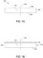
- FIGS. 1A through 1Cdepict a process flow according to some embodiments of the present invention.
- FIG. 2depicts a multilayer structure according to some embodiments of the present invention.
- FIG. 3depicts a multilayer structure according to some embodiments of the present invention.
- FIGS. 4A and 4Bdepict structures of exemplary flowable silazanes.
- FIG. 5depicts an exemplary structure of a flowable silsesquioxane.
- the present inventionis directed to a multi-layered semiconductor-on-insulator structure (SOI, e.g., a silicon-on-insulator structure) that resists impurities contained in a handle substrate from having an influence on the device.
- SOIsemiconductor-on-insulator structure
- the dielectric layer in the semiconductor-on-insulator structuremay comprise one or more insulating layers located between the handle substrate and the donor substrate or device layer.
- the one or more insulating layers in the SOI structure according to the present inventionmay include silicon nitride, silicon oxide, silicon oxynitride, and combinations of these materials.
- the dielectric layercomprises a multilayer comprising at least two insulating layers comprising these materials, or at least three insulating layers, or more insulating layers.
- the insulating layermay comprises an oxide-nitride-oxide dielectric (ONO) in which an oxide layer in interfacial contact with the handle substrate an a second oxide layer is in interfacial contact with the donor substrate or device layer.
- the nitride layeris between the two oxide layers.
- SOIsemiconductor-on-insulator structure
- ONOoxide-nitride-oxide dielectric layer
- the SOI structurecomprises a dielectric film layer stack including silicon nitride and silicon oxynitride. In some embodiments, the SOI structure comprises a dielectric film layer stack including silicon nitride and silicon oxynitride, and silicon oxide. In some embodiments, the method of the present invention deposits the layers in the stack as a single discrete deposition or a continuous graded deposition. The silicon nitride and/or silicon oxynitride in the layer stack may act as an etch stop, diffusion barrier, optical component, or hard mask.
- the substrates for use in the present inventioninclude a semiconductor handle substrate, e.g., a single crystal semiconductor handle wafer and a semiconductor donor substrate, e.g., a single crystal semiconductor donor wafer.
- the semiconductor device layer in a semiconductor-on-insulator composite structureis derived from the single crystal semiconductor donor wafer.
- the semiconductor device layermay be transferred onto the semiconductor handle substrate by wafer thinning techniques such as etching a semiconductor donor substrate or by cleaving a semiconductor donor substrate comprising a damage plane.
- one or more insulating layersmay be prepared on the surfaces of either or both the single crystal semiconductor handle wafer and the single crystal semiconductor donor wafer.
- FIGS. 1A through 1C , FIG. 2 , and FIG. 3depict a process flow according to some embodiments of the present invention.
- FIG. 1Aan exemplary, non-limiting single crystal semiconductor handle substrate or wafer 100 is depicted.
- the single crystal semiconductor handle wafer 100comprises two major, generally parallel surfaces. One of the parallel surfaces is a front surface 102 of the single crystal semiconductor handle wafer 100 , and the other parallel surface is a back surface 104 of the single crystal semiconductor handle wafer 100 .
- the single crystal semiconductor handle wafer 100comprises a circumferential edge 106 joining the front and back surfaces 102 , 104 .
- the single crystal semiconductor handle wafer 100comprise a central axis 108 perpendicular to the two major, generally parallel surfaces 102 , 104 and also perpendicular to a central plane defined by the points midway between the front and back surfaces 102 , 104 .
- the single crystal semiconductor handle wafer 100comprises a bulk region 110 between the two major, generally parallel surfaces 102 , 104 . Since semiconductor wafers, e.g., silicon wafers, typically have some total thickness variation (TTV), warp, and bow, the midpoint between every point on the front surface 102 and every point on the back surface 104 may not precisely fall within a plane.
- TTVtotal thickness variation
- the TTV, warp, and boware typically so slight that to a close approximation the midpoints can be said to fall within an imaginary central plane which is approximately equidistant between the front and back surfaces 102 , 104 .
- the front surface 102 and the back surface 104 of the single crystal semiconductor handle wafer 100may be substantially identical.
- a surfaceis referred to as a “front surface” or a “back surface” merely for convenience and generally to distinguish the surface upon which the operations of method of the present invention are performed.
- a “front surface” of a single crystal semiconductor handle wafer 100e.g., a single crystal silicon handle wafer, refers to the major surface of the substrate that becomes an interior surface of the bonded structure.
- a “back surface” of a single crystal semiconductor handle wafer 100e.g., a handle wafer, refers to the major surface that becomes an exterior surface of the bonded structure.
- a “front surface” of a single crystal semiconductor donor substraterefers to the major surface of the single crystal semiconductor donor substrate that becomes an interior surface of the bonded structure
- a “back surface” of a single crystal semiconductor donor substraterefers to the major surface that becomes an exterior surface of the bonded structure.
- one or more insulating layersmay be prepared on the front surfaces of either or both the single crystal semiconductor handle substrate 100 and the single crystal semiconductor donor substrate.
- the single crystal semiconductor donor substrateforms the semiconductor device layer of the semiconductor-on-insulator (e.g., silicon-on-insulator) composite structure.
- the single crystal semiconductor handle substrate and the single crystal semiconductor donor substratemay be single crystal semiconductor wafers.
- the semiconductor waferscomprise a material selected from the group consisting of silicon, silicon carbide, silicon germanium, gallium arsenide, gallium nitride, indium phosphide, indium gallium arsenide, germanium, and combinations thereof.
- the single crystal semiconductor wafers, e.g., the single crystal silicon handle wafer and single crystal silicon donor wafer, of the present inventiontypically have a nominal diameter of at least about 150 mm, at least about 200 mm, at least about 300 mm, or at least about 450 mm.
- Wafer thicknessesmay vary from about 250 micrometers to about 1500 micrometers, such as between about 300 micrometers and about 1000 micrometers, suitably within the range of about 500 micrometers to about 1000 micrometers. In some specific embodiments, the wafer thickness may be about 725 micrometers. In some embodiments, the wafer thickness may be about 775 micrometers.
- the single crystal semiconductor waferscomprise single crystal silicon wafers which have been sliced from a single crystal ingot grown in accordance with conventional Czochralski crystal growing methods or float zone growing methods.
- Czochralski crystal growing methodsor float zone growing methods.
- Such methods, as well as standard silicon slicing, lapping, etching, and polishing techniquesare disclosed, for example, in F. Shimura, Semiconductor Silicon Crystal Technology, Academic Press, 1989, and Silicon Chemical Etching, (J. Grabmaier ed.) Springer-Verlag, N.Y., 1982 (incorporated herein by reference).
- the wafersare polished and cleaned by standard methods known to those skilled in the art. See, for example, W. C.
- the single crystal silicon wafers of the present inventionare single crystal silicon wafers which have been sliced from a single crystal ingot grown in accordance with conventional Czochralski (“Cz”) crystal growing methods, typically having a nominal diameter of at least about 150 mm, at least about 200 mm, at least about 300 mm, or at least about 450 mm.
- CzCzochralski
- both the single crystal silicon handle wafer and the single crystal silicon donor waferhave mirror-polished front surface finishes that are free from surface defects, such as scratches, large particles, etc.
- Wafer thicknessmay vary from about 250 micrometers to about 1500 micrometers, such as between about 300 micrometers and about 1000 micrometers, suitably within the range of about 500 micrometers to about 1000 micrometers. In some specific embodiments, the wafer thickness may be between about 725 micrometers and about 800 micrometers, such as between about 750 micrometers and about 800 micrometers. In some embodiments, the wafer thickness may be about 725 micrometers. In some embodiments, the wafer thickness may be about 775 micrometers.
- the single crystal semiconductor wafersi.e., single crystal semiconductor handle wafer and single crystal semiconductor donor wafer, comprise interstitial oxygen in concentrations that are generally achieved by the Czochralski-growth method.
- the single crystal semiconductor waferscomprise oxygen in a concentration between about 4 PPMA and about 18 PPMA.
- the semiconductor waferscomprise oxygen in a concentration between about 10 PPMA and about 35 PPMA.
- the single crystal silicon wafercomprises oxygen in a concentration of no greater than about 10 PPMA. Interstitial oxygen may be measured according to SEMI MF 1188-1105.
- the single crystal semiconductor handle wafer 100may have any resistivity obtainable by the Czochralski or float zone methods. Accordingly, the resistivity of the single crystal semiconductor handle wafer 100 is based on the requirements of the end use/application of the structure of the present invention. The resistivity may therefore vary from milliohm or less to megaohm or more.
- the single crystal semiconductor handle wafer 100comprises a p-type or an n-type dopant. Suitable dopants include boron (p type), gallium (p type), phosphorus (n type), antimony (n type), and arsenic (n type). The dopant concentration is selected based on the desired resistivity of the handle wafer.
- the single crystal semiconductor handle substratecomprises a p-type dopant. In some embodiments, the single crystal semiconductor handle substrate is a single crystal silicon wafer comprising a p-type dopant, such as boron.
- the single crystal semiconductor handle wafer 100has a relatively low minimum bulk resistivity, such as below about 100 ohm-cm, below about 50 ohm-cm, below about 1 ohm-cm, below about 0.1 ohm-cm, or even below about 0.01 ohm-cm.
- the single crystal semiconductor handle substrate 100has a relatively low minimum bulk resistivity, such as below about 100 ohm-cm, or between about 1 ohm-cm and about 100 ohm-cm.
- Low resistivity wafersmay comprise electrically active dopants, such as boron (p type), gallium (p type), aluminum (p type), indium (p type), phosphorus (n type), antimony (n type), and arsenic (n type).
- the single crystal semiconductor handle wafer 100has a relatively high minimum bulk resistivity.
- High resistivity wafersare generally sliced from single crystal ingots grown by the Czochralski method or float zone method.
- High resistivity wafersmay comprise electrically active dopants, such as boron (p type), gallium (p type), aluminum (p type), indium (p type), phosphorus (n type), antimony (n type), and arsenic (n type), in generally very low concentrations.
- Cz-grown silicon wafersmay be subjected to a thermal anneal at a temperature ranging from about 600° C. to about 1000° C. in order to annihilate thermal donors caused by oxygen that are incorporated during crystal growth.
- the single crystal semiconductor handle waferhas a minimum bulk resistivity of at least 100 Ohm-cm, or even at least about 500 Ohm-cm, such as between about 100 Ohm-cm and about 100,000 Ohm-cm, or between about 500 Ohm-cm and about 100,000 Ohm-cm, or between about 1000 Ohm-cm and about 100,000 Ohm-cm, or between about 500 Ohm-cm and about 10,000 Ohm-cm, or between about 750 Ohm-cm and about 10,000 Ohm-cm, between about 1000 Ohm-cm and about 10,000 Ohm-cm, between about 1000 Ohm-cm and about 6000 ohm-cm, between about 2000 Ohm-cm and about 10,000 Ohm-cm, between about 3000 Ohm-cm and about 10,000 Ohm-cm, or between about 3000 Ohm-cm and about 5,000 Ohm-cm.
- 500 Ohm-cmsuch as between about 100 Ohm-cm and about 100,000 Ohm-cm, or between about 500 Ohm-
- the single crystal semiconductor handle substratehas a bulk resistivity between about 1000 Ohm-cm and about 6,000 Ohm-cm.
- Methods for preparing high resistivity wafersare known in the art, and such high resistivity wafers may be obtained from commercial suppliers, such as SunEdison Semiconductor Ltd. (St. Peters, Mo.; formerly MEMC Electronic Materials, Inc.).
- the single crystal semiconductor handle wafer 100may comprise single crystal silicon.
- the single crystal semiconductor handle wafer 100may have, for example, any of (100), (110), or (111) crystal orientation, and the choice of crystal orientation may be dictated by the end use of the structure.
- the front surface 102 , the back surface 104 , or bothmay be oxidized according to methods known in the art. Oxidation may be accomplished by means known in the art, such as thermal oxidation (in which some portion of the deposited semiconductor material film will be consumed) or CVD oxide deposition.
- the oxidation layer on the front surface 102 , the back surface 104 , or bothmay be at least about 1 nanometer thick, such as between about 10 nanometers and about 5000 nanometers thick, such as between about 100 nanometers and about 1000 nanometers, or between about 200 nanometers and about 400 nanometers.
- the oxidation layeris relatively thin, such as between about 5 angstroms and about 25 angstroms, such as between about 10 angstroms and about 15 angstroms.
- Thin oxide layerscan be obtained by exposure to a standard cleaning solution, such as an SC1/SC2 cleaning solution.
- the SC1 solutioncomprises 5 parts deioinized water, 1 part aqueous NH 4 OH (ammonium hydroxide, 29% by weight of NH 3 ), and part of aqueous H 2 O 2 (hydrogen peroxide, 30%).
- the handle substratemay be oxidized by exposure to an aqueous solution comprising an oxidizing agent, such as an SC2 solution.
- the SC2 solutioncomprises 5 parts deioinized water, 1 part aqueous HCl (hydrochloric acid, 39% by weight), and 1 pan of aqueous H 2 O 2 (hydrogen peroxide, 30%).
- a dielectric layer 420 comprising one or more insulating layers(e.g., three or more insulating layers, therein numbers 120 , 140 and 400 ) is prepared between a single crystal semiconductor handle substrate 100 and a single crystal semiconductor donor substrate 500 .
- a non-limiting, exemplary multi-layered semiconductor-on-insulator structure(SOI, e.g., a silicon on insulator structure) is depicted.
- the SOI structurecomprises a dielectric layer 420 comprising three insulating layers, e.g., an oxide-nitride-oxide dielectric layer (ONO), according to some embodiments of the present invention.
- SOIoxide-nitride-oxide dielectric layer
- the multi-layered semiconductor-on-insulator structurecomprises a single crystal semiconductor handle substrate 100 , a first semiconductor oxide layer 120 , a semiconductor nitride layer 140 , a second semiconductor oxide layer 400 , and a single crystal semiconductor donor substrate 500 .
- Other configurations of insulating layersfall within the scope of the present disclosure. For example, one or more insulating layers may be excluded from the dielectric layer, or additional insulating layers may be included. With reference to FIG.
- the bonding interfacecan be any of the following: (1) between the first semiconductor oxide layer 120 and the semiconductor nitride layer 140 , (2) between the semiconductor nitride layer 140 and the semiconductor second oxide layer 400 , and (3) between the first semiconductor oxide layer 120 and the second semiconductor oxide layer 400 if the structure lacks a nitride layer.
- the dielectric layer 420may comprise the ONO layers as depicted in FIG. 2 , or may comprise other structures comprising one or more layers of insulating material.
- the dielectric layer 420may be formed upon the front surface of the single crystal semiconductor handle substrate 100 or it may be formed upon the front surface of the single crystal semiconductor donor substrate 500 .
- portions of the dielectric layer 420may be contributed by insulating layers formed upon both the front surface of the single crystal semiconductor handle substrate 100 and the front surface of the single crystal semiconductor donor substrate 500 .
- the dielectric layer according to the present inventionmay comprise insulating materials selected from among silicon dioxide, silicon nitride, silicon oxynitride, hafnium oxide, titanium oxide, zirconium oxide, lanthanum oxide, barium oxide, and any combination thereof.
- the dielectric layercomprises one or more insulating material selected from the group consisting of silicon dioxide, silicon nitride, silicon oxynitride, and any combination thereof.
- the dielectric layerhas a thickness of at least about 10 nanometer thick, such as between about 10 nanometers and about 10,000 nanometers, between about 10 nanometers and about 5,000 nanometers, between 50 nanometers and about 400 nanometers, or between about 100 nanometers and about 400 nanometers, such as about 50 nanometers, 100 nanometers, or 200 nanometers.
- the dielectric layer 420comprises multiple layers of insulating material, for example, as depicted in FIG. 2 , although other configurations are within the scope of this invention.
- the dielectric layermay comprise two insulating layers, three insulating layers, or more.
- Each insulating layermay comprise a material selected from among silicon dioxide, silicon oxynitride, silicon nitride, hafnium oxide, titanium oxide, zirconium oxide, lanthanum oxide, barium oxide, and any combination thereof.
- each insulating layermay comprise a material selected from the group consisting of silicon dioxide, silicon nitride, siliconoxynitride, and any combination thereof.
- Each insulating layermay have a thickness of at least about 10 nanometer thick, such as between about 10 nanometers and about 10,000 nanometers, between about 10 nanometers and about 5,000 nanometers, between 50 nanometers and about 400 nanometers, or between about 100 nanometers and about 400 nanometers, such as about 50 nanometers, 100 nanometers, or 200 nanometers.
- the dielectric layercomprises two insulating layers, wherein the two insulating layers comprise silicon dioxide layer, silicon nitride, silicon oxynitride, or any combination thereof.
- the dielectric layercomprises two insulating layers prepared upon the front surface of a single crystal semiconductor donor substrate.
- the two layerscomprise a silicon dioxide layer in interfacial contact with the front surface of the single crystal semiconductor donor substrate (before the cleaving process) or the single crystal semiconductor device layer (after the cleaving process) and a silicon nitride layer in interfacial contact with the silicon dioxide layer.
- the dielectric layercomprises two insulating layers prepared upon the front surface of a single crystal semiconductor handle substrate.
- the dielectric layercomprises two insulating layers, one of which is prepared upon the front surface of a single crystal semiconductor handle substrate, and the other of which is prepared upon the front surface of a single crystal semiconductor donor substrate.
- Each insulating layer within a bilayer dielectric layermay have a thickness of at least about 10 nanometer thick, such as between about 10 nanometers and about 10,000 nanometers, between about 10 nanometers and about 5,000 nanometers, between 50 nanometers and about 400 nanometers, or between about 100 nanometers and about 400 nanometers, such as about 50 nanometers, 100 nanometers, or 200 nanometers.
- the dielectric layer 420comprises three insulating layers.
- the three insulating layerscomprise a silicon dioxide layer, a silicon nitride layer in interfacial contact with the silicon dioxide layer, and a silicon dioxide layer in interfacial contact with the silicon nitride layer.
- the dielectric layercomprises three insulating layers prepared upon the front surface of a single crystal semiconductor donor substrate.
- the dielectric layer 420comprises three insulating layers, wherein the three insulating layers comprise a silicon dioxide layer in interfacial contact with the front surface of the single crystal semiconductor donor substrate (before the cleaving process) or the single crystal semiconductor device layer (after the cleaving process), a silicon nitride layer in interfacial contact with the silicon dioxide layer, and a silicon dioxide layer in interfacial contact with the silicon nitride layer.
- the dielectric layercomprises three insulating layers prepared upon the front surface of a single crystal semiconductor handle substrate.
- the dielectric layercomprises three insulating layers, one or two of which are prepared upon the front surface of a single crystal semiconductor handle substrate, and the other one or two of which are prepared upon the front surface of a single crystal semiconductor donor substrate.
- Each insulating layer within a trilayer dielectric layermay have a thickness of at least about 10 nanometer thick, such as between about 10 nanometers and about 10,000 nanometers, between about 10 nanometers and about 5,000 nanometers, between 50 nanometers and about 400 nanometers, or between about 100 nanometers and about 400 nanometers, such as about 50 nanometers, 100 nanometers, or 200 nanometers.
- At least a portion, i.e., one, two, three or more insulating layers, of the dielectric layeris formed upon the front surface 102 of the single crystal semiconductor handle substrate 100 .
- an insulating layer 120 comprising a flowable or reflowable materialis deposited upon the front surface 102 of the single crystal semiconductor handle substrate 100 .
- an additional insulating layer 140which may be an oxide layer, an oxynitride layer, or a nitride layer, may be deposited upon the insulating layer 120 comprising a flowable or reflowable material.
- the handle substrate 100 comprising the insulating layer 120 comprising a flowable or reflowable materialis not subjected to further deposition, and the insulating layer 120 comprising a flowable or reflowable material is useful as the bonding interface, thereby taking advantage of the flowable or reflowable insulating layer's planarizing properties, which reduces roughness/voids in the bonding region.
- the flowable or reflowable materialmay be deposited on the front surface of the single crystal semiconductor donor substrate.
- an insulating layer comprising a reflowable materialis deposited upon the front surface 102 of the single crystal semiconductor handle substrate 100 .
- a reflowable insulating layercomprises a material capable of flowing at a temperature of less than about 1000° C.
- a curing stepmay be employed in order to smooth and planarize an insulating layer comprising a reflowable material. Reflowable behavior of films occurs due to heating the layer after deposition for void free planarization. Doped films are a common way to lower the glass transition temperature. By allowing the film to “reflow” at high temperatures, voids may disappear, and bond strength due to the added contact is expected.
- an insulating layercomprising a flowable material is deposited upon the front surface 102 of the single crystal semiconductor handle substrate 100 .
- a flowable insulating layertends to smooth and planarize during its deposition and reduce roughness. Based on the geometry of the material, the thickness of deposited film changes. Generally, surface tension dictates that the film will be thicker at concave geometries and thinner at convex areas.
- Flowable filmsmay be deposited by solvent based spin on, or low temperature condensation reactions. Flowable films have the unique ability to planarize features and reduce roughness.
- the flowable insulating layercomprises a flowable oxide. Flowable oxides include polymer precursors that have been dissolved or functionalized. By virtue of the solution or the activity of the polymer once deposited, it has the ability to move on the wafer surface. Two general application techniques are used, spin on dielectrics or CVD.
- the flowable insulating layercomprises a flowable silazane.
- Polysilazanesare polymers that comprise a polymer backbone comprising generally alternating silicon and nitrogen atoms. Flowable silazanes may be cured to remove NH 3 when pure undoped silica glass is required. Suitable dissolved polysilazane materials may be acquired from AZ Electronic Materials, Dow Chemical, and Sigma Aldrich. A suitable spin on tool may be acquired from Tokyo Electron Limited. Subsequent curing and annealing is common after deposition of the flowable silazane. Structures of exemplary flowable silazanes are depicted in FIGS. 4A and 4B . FIG.
- FIG. 4Adepicts a non-derivatized flowable silazane. If all substituents R are H atoms, the polymer is designated as Perhydropolysilazane, Polyperhydridosilazane, or Inorganic Polysilazane ([H 2 Si—NH]n).
- FIG. 4Bdepicts a flowable silazane derivatized with R groups.
- the R groupcomprises hydrocarbyl having from one to 12 carbon atoms, such as alkyl groups having from one to 12 carbon atoms, e.g., methyl, ethyl, n-propyl, isopropyl, butyl, etc.
- the R groupcomprises aromatic groups having from three to 12 carbon atoms, e.g., phenyl, naphthyl, etc.
- the flowable insulating layercomprises a flowable silsesquioxane.
- Silsesquioxanesare flowable silicon oxides.
- a silsesquioxaneis an organosilicon compound with the chemical formula [RSiO 3 /2]n (R ⁇ H, alkyl, aryl or alkoxyl).
- the R groupcomprises hydrocarbyl having from one to 12 carbon atoms, such as alkyl groups having from one to 12 carbon atoms, e.g., methyl, ethyl, n-propyl, isopropyl, butyl, etc.
- the R groupcomprises alkoxy from one to 12 carbon atoms, e.g., methoxy, ethoxy, n-propoxy, isopropoxy, butoxy, etc.
- the R groupcomprises aromatic groups having from three to 12 carbon atoms, e.g., phenyl, naphthyl, etc.
- Silsesquioxanesare colorless solids that adopt cage-like or polymeric structures with Si—O—Si linkages and tetrahedral Si vertices. Silsesquioxanes are known in molecular form with 6, 8, 10, and 12 Si vertices, as well as polymers.
- a reflowable insulating layercomprises a doped oxide.
- reflowable insulating layercomprises a silicate glass selected from the group consisting of phosphosilicate glass, borosilicate glass, borophosphosilicate glass (BPSG), and any combination thereof.
- Doped glassesare common in the industry to lower the glass transition temperature. By allowing the film to “reflow” at high temperatures, one may fill small voids or gaps.
- an insulating layer 120 comprising a flowable or reflowable materialis deposited by contacting the front surface of the single crystal semiconductor handle substrate with a solution comprising oxide precursor and/or non-oxide precursor.
- oxide precursor and/or non-oxide precursorfor example, silsesquioxanes are commonly prepared from hydrolytic condensation reactions of trifunctional organosilicon monomers, e.g., RSiCl 3 or RSi(OMe) 3 .
- Various alternativesare available with different structures or functional modification with organics.
- Silazanesare commonly available as monomers, and also offer the potential to be converted to oxide. There are also precursors commercially available for other nitrides, carbides, and borides.
- the insulating layer 120 comprising a flowable or reflowable materialhas a thickness between about 50 nanometers and about 1 micrometer, between about 100 nanometers and about 1 micrometer.
- An insulating layer 120comprising a flowable or reflowable material may be annealed to thereby reflow, cure, and/or densify the film. Both flowable and reflow films can be densified. Only reflowable films flow during an anneal. During densification of a reflowable insulating layer, such as doped oxides (like borophosphosilicate glass, BPSG), they reflow.
- a reflowable materialcan smooth the surface, thereby decreasing surface roughness and rendering the surface more amenable to bonding.
- Flowable polymersonly flow during deposition, and a subsequent cure locks it into place.
- Curing a flowable insulating layermay cause densification in the range of between about 5% and about 20%. Densification anneals may not change the thickness of measurement of density, but is usually used to chemically change the film, thereby making resistant to chemical etch.
- a flowable oxide insulating layermay be cured to remove residual solvent from the spin on process. Additionally, an as-deposited layer may be reactive after deposition, and a cure may redistribute NH, SiN, Si—O and Si—H bonds. The reaction mechanism responsible for the chemical changes is induced by heating in various ambient atmospheres, generally an oxidizing atmosphere. Curing of flowables is accompanied by weight loss, density, and change in dielectric properties. For certain applications, one might be interested in densification until it is very similar to thermal oxide.
- curing of the insulating layer 120 comprising a flowable or reflowable materialmay occur by contacting the layer with ozone.
- the ozonemay be dissolved in water, or the insulating layer 12 may be exposed to an ozone containing ambient atmosphere.
- curing of an insulating layer 120 comprising a flowable or reflowable materialmay occur by irradiating the layer with ultraviolet light, such as light having a wavelength between about 185 nanometers and about 256 nanometers, depending upon the composition of the insulating layer.
- an insulating layer 120 comprising a flowable or reflowable materialis cured by annealing the single crystal semiconductor handle substrate having the insulating layer on the front surface thereof, for example at a temperature between about 800° C. and about 1000° C., depending upon the composition of the insulating layer and the dopant concentration.
- Cure and/or densification of the insulating layer 120 comprising a flowable or reflowable materialmay decrease the surface roughness.
- the surface roughness according to the root mean square method over a 2 micrometer by 2 micrometer surface area, RMS 2 ⁇ 2 um2is preferably less than about 2 angstroms, such as between about 1 angstrom and about 2 angstroms, wherein root mean squared is calculated according to the following equation:
- the roughness profilecontains ordered, equally spaced points along the trace, and y, is the vertical distance from the mean line to the data point. At a surface roughness of preferably less than 2 angstroms, the surface is ready for bonding or optional oxidation.
- one or more insulating layersmay be prepared upon the front surface of the single crystal semiconductor handle substrate 100 or upon the front surface of a single crystal semiconductor donor substrate by a plasma deposition process, such as plasma enhanced chemical vapor deposition.
- a plasma deposition processsuch as plasma enhanced chemical vapor deposition.
- an insulating layer comprising a semiconductor oxidee.g., silicon oxide
- an insulating layer comprising a semiconductor nitridee.g., silicon nitride
- an insulating layer comprising a semiconductor oxynitridee.g., silicon oxynitride
- a plasma treatmentcomprising nitrogen and oxygen precursors.
- a wide variety of substrate configurationsmay be subjected to oxygen plasma treatment and/or nitrogen plasma treatment.
- the front surface 102 of the single crystal semiconductor handle substrate 100may be subjected to oxygen plasma treatment and/or nitrogen plasma treatment to thereby deposit a semiconductor oxide (e.g., silicon oxide), a semiconductor nitride (e.g., silicon nitride), or a semiconductor oxynitride (e.g., silicon oxynitride).
- a semiconductor oxidee.g., silicon oxide
- a semiconductor nitridee.g., silicon nitride
- a semiconductor oxynitridee.g., silicon oxynitride
- One or more insulating layersmay be deposited by plasma deposition on the front surface 102 of the single crystal semiconductor handle substrate 100 .
- an insulating layer 120comprising a flowable or reflowable material or an insulating layer 140 may be subjected to oxygen plasma treatment and/or nitrogen plasma treatment to deposit one or more additional insulating layers.
- one or more insulating layersmay be deposited upon the single crystal semiconductor donor substrate by plasma deposition.
- the oxygen plasma and/or nitrogen plasma surface activation toolis a commercially available tool, such as those available from EV Group, such as EVG®810LT Low Temp Plasma Activation System.
- General requirements of a plasma enhanced CVD chamberinclude a reactor with various electrode designs, power generation electronics, impedance matching network to transfer power to the gas load, mass flow controllers for input gasses, and pressure control systems. Typical systems are vertical tube reactors powered by an inductively coupled RF source.
- the single crystal semiconductor handle substrate 100 and/or donor substrateis loaded into the chamber and placed on a heated support chamber.
- the chamberis evacuated and backfilled with an oxygen gas source and/or a nitrogen gas source in a carrier gas, such as argon, to a pressure less than atmospheric to thereby create the plasma.
- Oxygen and/or waterare suitable source gases for plasma oxide treatment.
- Ammonia and/or nitrogen and/or nitric oxide (NO) and/or nitrous oxide (N 2 O) gasare suitable source gases for plasma nitride treatment.
- Oxynitride filmsmay be deposited by including oxygen and nitrogen gas sources. Additionally, the use of nitric oxide or nitrous oxide additionally incorporates oxygen in to the insulating layer, thereby depositing an oxynitride film.
- suitable silicon precursorsinclude methyl silane, silicon tetrahydride (silane), trisilane, disilane, pentasilane, neopentasilane, tetrasilane, dichlorosilane (SiH 2 Cl 2 ), trichlorosilane (SiHCl 3 ), silicon tetrachloride (SiCl 4 ), among others.
- Aris added as a carrier gas.
- a single crystal semiconductor handle substrate 100 or a single crystal silicon donor substrateis subjected to plasma treatment to deposit and insulating layer comprising semiconductor nitride (e.g., silicon nitride) or semiconductor oxynitride (e.g., silicon oxynitride).
- the substratesmay be subjected to plasma deposition without any additional layers.
- one or more insulating layersmay be deposited upon the substrates, and plasma enhanced CVD may be used to deposit additional insulating layers upon the insulating layers deposited according to other techniques.
- Plasma depositionmay be varied to tune the properties of the semiconductor nitride (e.g., silicon nitride) or semiconductor oxynitride (e.g., silicon oxynitride).
- the pressure, flow rate, temperature, and relative ratio of precursorse.g., ratio of NH 3 to N 2 O gases, may tune the silicon and nitride molar ratios of the plasma deposited nitride layer.
- inclusion of an oxygen precursorincorporates oxygen to prepare an oxynitride layer.
- plasma depositionmay occur in an ambient atmosphere comprising silicon and nitrogen precursors to thereby deposit a silicon nitride layer on the handle substrate and/or donor substrate.
- an oxygen precursormay be introduced into the atmosphere to thereby deposit oxynitride.
- the oxygen concentration in the handle semiconductor oxynitride layermay vary according to a gradient, whereby the oxygen concentration is low at the interface with the handle semiconductor nitride layer and increases in the perpendicular direction away from the surface of the handle semiconductor oxynitride layer.
- the flow of the nitrogen precursormay be ceased and deposition may continue only with silicon precursor and an oxygen gas source to thereby deposit an insulating layer comprising semiconductor oxide, e.g., silicon oxide.
- a dielectric layermay be deposited by plasma techniques comprising a semiconductor nitride (e.g., silicon nitride) layer and a semiconductor oxynitride (e.g., silicon oxynitride) layer.
- a dielectric layermay be deposited by plasma techniques comprising a semiconductor nitride (e.g., silicon nitride) layer, a semiconductor oxynitride (e.g., silicon oxynitride) layer, and a semiconductor oxide (e.g., silicon oxide) layer.
- plasma deposition of a dielectric layer comprising multiple insulating layersmay occur continuously, i.e., without interruption, by varying the ratios and identities of the process gases.
- the plasma deposited semiconductor nitridee.g., silicon nitride
- semiconductor oxynitridee.g., silicon oxynitride
- semiconductor oxidee.g., silicon oxide
- Plasma depositionmay occur at a temperature between about 20° C. and about 400° C.
- Insulating layers having a thickness between about 500 angstroms and about 10,000 angstromscan be deposited by PECVD at a rate between about 100 angstroms/minute and about 1000 angstroms/minute.
- the flow rate ratios of the gaseous silicon precursor and the gaseous nitrogen precursormay be between about 1/200 and about 1/50, such as about 1/100. These ratios may yield a silicon nitride layer having a molar ratio of silicon to nitride of between about 0.7 and about 1.8.
- Oxygenmay be incorporated in the plasma process, by adding an oxygen containing species such as oxygen or NO.
- the layermay transition from semiconductor nitride (e.g., silicon nitride) to semiconductor oxynitride (e.g., silicon oxynitride) of increasing oxygen concentration to semiconductor oxide (e.g., silicon oxide).
- semiconductor nitridee.g., silicon nitride
- semiconductor oxynitridee.g., silicon oxynitride
- the refractive index of the insulating layersmay be tuned in the range between about 1.2 and about 3, such as between about 1.4 and about 2, or between about 1.5 and about 2.
- Post processing anneal and chemical vapor deposition of silicon oxide, SiO 2is possible to further tune the bond interface or hydrogen content of the film.
- the bonding between the handle substrate and the donor substratebenefits from roughness of less than about 5 angstroms, according to the root mean square method over a 2 micrometer by 2 micrometer surface area, RMS 2x2 um2 . Generally this can be achieved in a plasma deposition with controlled inductively coupled plasma and lowering the bias power below the roughening threshold. Successful layer transfer has been demonstrated on plasma deposited films with roughness of about 5 angstroms or less.
- Silicon oxynitridecomprises a material having a composition that has a chemical formula Si x O y N z .
- the values of x, y, and zmay vary continuously between SiO 2 (silicon dioxide) and Si 3 N 4 (silicon nitride). Accordingly, in a silicon oxynitride layer, the values of y and z are both greater than 0.
- a known crystalline form of silicon oxynitrideis Si 2 ON 2 .
- the silicon oxynitridemay be deposited in a gradient fashion, such that the composition of the film and thus the refractive index of the film may vary in a gradient fashion.
- silicon oxynitridemay be deposited upon a silicon nitride film by the gradual introduction of an oxygen precursor (e.g., oxygen, water, N 2 O) into the plasma deposition ambient atmosphere, which may comprise a silicon precursor and a nitrogen precursor, e.g., ammonia.
- an oxygen precursore.g., oxygen, water, N 2 O
- the ratio of NH 3 :N 2 Omay be varied, that is, lowered, during deposition to gradually increase the oxygen content in the silicon oxynitride layer.
- the atmospherecontains silicon precursors and oxygen precursors, which enables deposition of a silicon dioxide layer on the silicon oxynitride layer.
- the refractive index range of the silicon oxynitride filmmay vary between 2.0 for silicon nitride and 1.45 for silicon dioxide.
- Silicon nitride produced from plasmais structurally distinct from silicon nitride deposited according to conventional chemical or physical vapor deposition techniques. Conventional CVD or PVD deposition generally results in a silicon nitride layer having a stoichiometry of Si 3 N 4 .
- Plasma processescan be controlled to deposit a film having a composition such as Si x N y H z depending on the ratios of input reactant gasses, power level, substrate temperature, and overall reactor pressure. Pathways in a plasma system exist to form Si—N, Si ⁇ N and Si ⁇ N bonds. This is due to the fact that plasma energies are a hammer that produce Si x H z and N y H z species.
- the refractive index and optical gapchange dramatically with the Si/N ratio.
- the filmsbecome Si rich and may reach an index of refraction up to 3.0 (compared to 2 for LPCVD).
- Other properties that may be influencedinclude dielectric constant, breakdown, mechanical, and chemical (etch rate).
- the single crystal semiconductor handle substrate 100e.g. a single crystal semiconductor handle wafer such as a single crystal silicon handle wafer, prepared according to the method described herein is next bonded to a semiconductor donor substrate 500 , e.g., a single crystal semiconductor donor wafer, which is prepared according to conventional layer transfer methods.
- the single crystal semiconductor donor substrate 500may be a single crystal semiconductor wafer.
- the semiconductor wafercomprises a material selected from the group consisting of silicon, silicon carbide, silicon germanium, gallium arsenide, gallium nitride, indium phosphide, indium gallium arsenide, germanium, and combinations thereof.
- the single crystal semiconductor (e.g., silicon) donor wafer 500may comprise electrically active dopants, such as boron (p type), gallium (p type), aluminum (p type), indium (p type), phosphorus (n type), antimony (n type), and arsenic (n type).
- the resistivity of the single crystal semiconductor (e.g., silicon) donor wafermay range from 1 to 50 Ohm-cm, typically, from 5 to 25 Ohm-cm.
- the single crystal semiconductor donor wafer 500may be subjected to standard process steps including oxidation, implant, and post implant cleaning.
- a semiconductor donor substrate 500such as a single crystal semiconductor wafer of a material that is conventionally used in preparation of multilayer semiconductor structures, e.g., a single crystal silicon donor wafer, that has been etched and polished and optionally oxidized, is subjected to ion implantation to form a damage layer in the donor substrate.
- the single crystal semiconductor donor substrate 500comprises a dielectric layer 400 .
- the dielectric layer 400may comprise one or more insulating layers formed on the front surface of the single crystal semiconductor donor substrate 500 .
- the dielectric layer 420comprises multiple layers of insulating material, for example, as depicted in FIG. 2 , although other configurations are within the scope of this invention.
- Each insulating layermay comprise a material selected from among silicon dioxide, silicon nitride, hafnium oxide, titanium oxide, zirconium oxide, lanthanum oxide, barium oxide, and a combination thereof.
- each insulating layermay comprise a material selected from the group consisting of silicon dioxide, silicon nitride, and siliconoxynitride.
- Each insulating layermay have a thickness of at least about 10 nanometer thick, such as between about 10 nanometers and about 10,000 nanometers, between about 10 nanometers and about 5,000 nanometers, between 50 nanometers and about 400 nanometers, or between about 100 nanometers and about 400 nanometers, such as about 50 nanometers, 100 nanometers, or 200 nanometers.
- the dielectric layer 420comprises three layers. One, two, or three of the layers may be formed upon the single crystal semiconductor handle substrate 100 . One, two, or three of the layers may be formed upon the single crystal semiconductor donor substrate 500 . Still further, one or two of the layers may be formed upon the single crystal semiconductor handle substrate 100 , and one or two of the layers may be formed upon the single crystal semiconductor donor substrate 500 .
- the front surface of the single crystal semiconductor donor substrate 500may be thermally oxidized (in which some portion of the deposited semiconductor material film will be consumed) to prepare the semiconductor oxide film, or the semiconductor oxide (e.g., silicon dioxide) film may be grown by CVD oxide deposition.
- the front surface of the single crystal semiconductor donor substrate 500may be thermally oxidized in a furnace such as an ASM A400 in the same manner described above.
- the single crystal semiconductor donor substrate 500is oxidized to provide an oxide layer on the front surface layer of at least about 1 nanometer thick, about 10 nanometer thick, such as between about 10 nanometers and about 10,000 nanometers, between about 10 nanometers and about 5,000 nanometers, or between about 100 nanometers and about 400 nanometers.
- the oxidation layer on the single crystal semiconductor donor substrate 500is relatively thin, such as between about 5 angstroms and about 25 angstroms, such as between about 10 angstroms and about 15 angstroms. Thin oxide layers can be obtained by exposure to a standard cleaning solution, such as an SC1/SC2 cleaning solution.
- Ion implantationmay be carried out in a commercially available instrument, such as an Applied Materials Quantum II, a Quantum LEAP, or a Quantum X.
- Implanted ionsinclude He, H, H 2 , or combinations thereof.
- Ion implantationis carried out as a density and duration sufficient to form a damage layer in the semiconductor donor substrate.
- Implant densitymay range from about 10 12 ions/cm 2 to about 10 17 ions/cm 2 , such as from about 10 14 ions/cm 2 to about 10 17 ions/cm 2 , such as from about 10 15 ions/cm 2 to about 10 16 ions/cm 2 .
- Implant energiesmay range from about 1 keV to about 3,000 keV, such as from about 10 keV to about 3,000 keV. Implant energies may range from about 1 keV to about 3,000 keV, such as from about 5 keV to about 1,000 keV, or from about 5 keV to about 200 keV, or from 5 keV to about 100 keV, or from 5 keV to about 80 keV.
- the depth of implantationdetermines the thickness of the single crystal semiconductor device layer in the final SOI structure.
- the ionsmay be implanted to a depth between about 100 angstroms and about 30,000 angstroms, such as between about 200 angstroms and about 20,000 angstroms, such as between about 2000 angstroms and about 15,000 angstroms, or between about 15,000 angstroms and about 30,000 angstroms.
- the cleancould include a Piranha clean followed by a DI water rinse and SC1/SC2 cleans.
- the single crystal semiconductor donor substrate 500 having an ion implant region therein formed by He + , H + , H 2 + , and any combination thereof ion implantis annealed at a temperature sufficient to form a thermally activated cleave plane in the single crystal semiconductor donor substrate.
- a suitable toolmight be a simple Box furnace, such as a Blue M model.
- the ion implanted single crystal semiconductor donor substrateis annealed at a temperature of from about 200° C. to about 350° C., from about 225° C. to about 325° C., preferably about 300° C.
- Thermal annealingmay occur for a duration of from about 2 hours to about 10 hours, such as from about 2 hours to about 8 hours. Thermal annealing within these temperatures ranges is sufficient to form a thermally activated cleave plane. After the thermal anneal to activate the cleave plane, the single crystal semiconductor donor substrate surface is preferably cleaned.
- the ion-implanted and optionally cleaned and optionally annealed single crystal semiconductor donor substrateis subjected to oxygen plasma and/or nitrogen plasma surface activation.
- the oxygen plasma surface activation toolis a commercially available tool, such as those available from EV Group, such as EVG®810LT Low Temp Plasma Activation System.
- the ion-implanted and optionally cleaned single crystal semiconductor donor waferis loaded into the chamber.
- the chamberis evacuated and backfilled with O 2 to a pressure less than atmospheric to thereby create the plasma.
- the single crystal semiconductor donor waferis exposed to this plasma for the desired time, which may range from about 1 second to about 120 seconds.
- Oxygen plasma surface oxidationis performed in order to render the front surface of the single crystal semiconductor donor substrate hydrophilic and amenable to bonding to a single crystal semiconductor handle substrate prepared according to the method described above.
- each of the front surface of the single crystal semiconductor donor substrate 500 and the front surface of single crystal semiconductor handle substrate 100may comprise one or more insulating layers.
- the insulating layersform the dielectric layer of the bonded structure.
- an exemplary dielectric layer 420is shown. As depicted therein, the dielectric layer 420 of the bonded structure may comprise a first oxide layer 120 , a nitride layer 140 , a second oxide layer 400 . Further configurations are within the scope of this disclosure.
- the bonded structuremay be further annealed to solidify the bond between the single crystal semiconductor donor substrate 500 and the single crystal semiconductor handle substrate 100 .
- the bonded structureis annealed at a temperature sufficient to form a thermally activated cleave plane in the single crystal semiconductor donor substrate.
- An example of a suitable toolmight be a simple Box furnace, such as a Blue M model.
- the bonded structureis annealed at a temperature of from about 200° C. to about 400° C., from about 300° C. to about 400° C., such as from about 350° C. to about 400° C.
- the annealmay occur at relatively high pressures, such as between about 0.5 MPa and about 200 MPa, such as between about 0.5 MPa and about 100 MPa, such as between about 0.5 MPa and about 50 MPa, or between about 0.5 MPa and about 10 MPa, or between about 0.5 MPa and about 5 MPa.
- the temperatureis likely limited by the “autocleave”. This occurs when the pressure of the platelets at the implant plane exceeds the external isostatic pressure. Accordingly, conventional anneal may be limited to bonding temperatures between about 350° C. and about 400° C. because of autocleave. After implantation and bond, the wafers are weakly held together. But the gap between the wafers is sufficient to prevent gas penetration or escape.
- Weak bondscan be strengthened by heat treatments, but the cavities formed during implant are filled with gas. While heating, the gas inside the cavities pressurizes. It is estimated that the pressure may reach 0.2-1 GPa (Cherkashin et al., J. Appl. Phys. 118, 245301 (2015)), depending on the dosage. When the pressure exceeds a critical value, the layer delaminates. This is referred to as an autocleave or thermal cleave. It prevents higher temperature or longer time in the anneal.
- bondingoccurs at elevated pressures, e.g., between about 0.5 MPa and about 200 MPa, such as between about 0.5 MPa and about 100 MPa, such as between about 0.5 MPa and about 50 MPa, or between about 0.5 MPa and about 10 MPa, or between about 0.5 MPa and about 5 MPa, which thereby enables bonding at elevated temperatures.
- the bonded structureis annealed at a temperature of from about 300° C. to about 700° C., from about 400° C. to about 600° C., such as between about 400° C. and about 450° C., or even between about 450° C. and about 600° C., or between about 350° C. and about 450° C.
- Thermal annealingmay occur for a duration of from about 0.5 hours to about 10 hour, such as between about 0.5 hours and about 3 hours, preferably a duration of about 2 hours. Thermal annealing within these temperatures ranges is sufficient to form a thermally activated cleave plane.
- the edge of both the handle wafer and donor wafermay become far apart due to the roll off. In this area, there is no layer transfer. It is called the terrace. Pressurized bonding is expected to reduce this terrace, extending the SOI layer further out towards the edge. The mechanism is based on trapped pockets of air being compressed and “zippering” outwards. After the thermal anneal to activate the cleave plane, the bonded structure may be cleaved.
- the bond between the single crystal single crystal semiconductor donor substrate 500 and the single crystal semiconductor handle substrate 100is strong enough to initiate layer transfer via cleaving the bonded structure at the cleave plane.
- Cleavingmay occur according to techniques known in the art.
- the bonded structuremay be placed in a conventional cleave station affixed to stationary suction cups on one side and affixed by additional suction cups on a hinged arm on the other side.
- a crackis initiated near the suction cup attachment and the movable arm pivots about the hinge cleaving the wafer apart.
- Cleavingremoves a portion of the semiconductor donor wafer, thereby leaving a single crystal semiconductor device layer 600 , preferably a silicon device layer, on the semiconductor-on-insulator composite structure. See FIG. 3 .
- the cleaved structuremay be subjected to a high temperature anneal in order to further strengthen the bond between the transferred device layer 600 and the single crystal semiconductor handle substrate 100 .
- a suitable toolmight be a vertical furnace, such as an ASM A400.
- the bonded structureis annealed at a temperature of from about 1000° C. to about 1200° C., preferably at about 1000° C. Thermal annealing may occur for a duration of from about 0.5 hours to about 8 hours, preferably a duration of about 4 hours. Thermal annealing within these temperatures ranges is sufficient to strengthen the bond between the transferred device layer and the single crystal semiconductor handle substrate.
- the bonded structuremay be subjected to a cleaning process designed to remove thin thermal oxide and clean particulates from the surface.
- the single crystal semiconductor device layermay be brought to the desired thickness and smoothness by subjecting to a vapor phase HCl etch process in a horizontal flow single wafer epitaxial reactor using H 2 as a carrier gas.
- the semiconductor device layer 600may have a thickness between about 20 nanometers and about 3 micrometers, such as between about 20 nanometers and about 2 micrometers, such as between about 20 nanometers and about 1.5 micrometers or between about 1.5 micrometers and about 3 micrometers.
- an epitaxial layermay be deposited on the transferred single crystal semiconductor device layer 600 .
- a deposited epitaxial layermay comprise substantially the same electrical characteristics as the underlying single crystal semiconductor device layer 600 .
- the epitaxial layermay comprise different electrical characteristics as the underlying single crystal semiconductor device layer 600 .
- An epitaxial layermay comprise a material selected from the group consisting of silicon, silicon carbide, silicon germanium, gallium arsenide, gallium nitride, indium phosphide, indium gallium arsenide, germanium, and combinations thereof.
- the epitaxial layermay comprise electrically active dopants, such as boron (p type), gallium (p type), aluminum (p type), indium (p type), phosphorus (n type), antimony (n type), and arsenic (n type).
- the resistivity of the epitaxial layermay range from 1 to 50 Ohm-cm, typically, from 5 to 25 Ohm-cm.
- the epitaxial layermay have a thickness between about 20 nanometers and about 3 micrometers, such as between about 20 nanometers and about 2 micrometers, such as between about 20 nanometers and about 1.5 micrometers or between about 1.5 micrometers and about 3 micrometers.
- the finished SOI wafercomprises the single crystal semiconductor handle substrate 100 , the dielectric layer 420 , and the semiconductor device layer 600 , may then be subjected to end of line metrology inspections and cleaned a final time using typical SC1-SC2 process.
Landscapes
- Engineering & Computer Science (AREA)
- Physics & Mathematics (AREA)
- Microelectronics & Electronic Packaging (AREA)
- General Physics & Mathematics (AREA)
- Manufacturing & Machinery (AREA)
- Computer Hardware Design (AREA)
- Condensed Matter Physics & Semiconductors (AREA)
- Power Engineering (AREA)
- Plasma & Fusion (AREA)
- Chemical & Material Sciences (AREA)
- Chemical Kinetics & Catalysis (AREA)
- Recrystallisation Techniques (AREA)
- Formation Of Insulating Films (AREA)
- Crystals, And After-Treatments Of Crystals (AREA)
Abstract
Description
Claims (36)
Priority Applications (1)
| Application Number | Priority Date | Filing Date | Title |
|---|---|---|---|
| US16/079,373US11114332B2 (en) | 2016-03-07 | 2017-03-03 | Semiconductor on insulator structure comprising a plasma nitride layer and method of manufacture thereof |
Applications Claiming Priority (3)
| Application Number | Priority Date | Filing Date | Title |
|---|---|---|---|
| US201662304381P | 2016-03-07 | 2016-03-07 | |
| US16/079,373US11114332B2 (en) | 2016-03-07 | 2017-03-03 | Semiconductor on insulator structure comprising a plasma nitride layer and method of manufacture thereof |
| PCT/US2017/020634WO2017155808A1 (en) | 2016-03-07 | 2017-03-03 | Semiconductor on insulator structure comprising a plasma nitride layer and method of manufacture thereof |
Related Parent Applications (1)
| Application Number | Title | Priority Date | Filing Date |
|---|---|---|---|
| PCT/US2017/020634A-371-Of-InternationalWO2017155808A1 (en) | 2016-03-07 | 2017-03-03 | Semiconductor on insulator structure comprising a plasma nitride layer and method of manufacture thereof |
Related Child Applications (1)
| Application Number | Title | Priority Date | Filing Date |
|---|---|---|---|
| US16/864,296DivisionUS11984348B2 (en) | 2016-03-07 | 2020-05-01 | Semiconductor on insulator structure comprising a plasma nitride layer and method of manufacture thereof |
Publications (2)
| Publication Number | Publication Date |
|---|---|
| US20190067085A1 US20190067085A1 (en) | 2019-02-28 |
| US11114332B2true US11114332B2 (en) | 2021-09-07 |
Family
ID=58358931
Family Applications (3)
| Application Number | Title | Priority Date | Filing Date |
|---|---|---|---|
| US16/079,373Active2037-08-23US11114332B2 (en) | 2016-03-07 | 2017-03-03 | Semiconductor on insulator structure comprising a plasma nitride layer and method of manufacture thereof |
| US16/864,296Active2037-03-27US11984348B2 (en) | 2016-03-07 | 2020-05-01 | Semiconductor on insulator structure comprising a plasma nitride layer and method of manufacture thereof |
| US18/631,819PendingUS20240258156A1 (en) | 2016-03-07 | 2024-04-10 | Semiconductor on insulator structure comprising a plasma nitride layer and method of manufacture thereof |
Family Applications After (2)
| Application Number | Title | Priority Date | Filing Date |
|---|---|---|---|
| US16/864,296Active2037-03-27US11984348B2 (en) | 2016-03-07 | 2020-05-01 | Semiconductor on insulator structure comprising a plasma nitride layer and method of manufacture thereof |
| US18/631,819PendingUS20240258156A1 (en) | 2016-03-07 | 2024-04-10 | Semiconductor on insulator structure comprising a plasma nitride layer and method of manufacture thereof |
Country Status (2)
| Country | Link |
|---|---|
| US (3) | US11114332B2 (en) |
| WO (1) | WO2017155808A1 (en) |
Families Citing this family (293)
| Publication number | Priority date | Publication date | Assignee | Title |
|---|---|---|---|---|
| US9394608B2 (en) | 2009-04-06 | 2016-07-19 | Asm America, Inc. | Semiconductor processing reactor and components thereof |
| US20130023129A1 (en) | 2011-07-20 | 2013-01-24 | Asm America, Inc. | Pressure transmitter for a semiconductor processing environment |
| US10714315B2 (en) | 2012-10-12 | 2020-07-14 | Asm Ip Holdings B.V. | Semiconductor reaction chamber showerhead |
| US20160376700A1 (en) | 2013-02-01 | 2016-12-29 | Asm Ip Holding B.V. | System for treatment of deposition reactor |
| US11015245B2 (en) | 2014-03-19 | 2021-05-25 | Asm Ip Holding B.V. | Gas-phase reactor and system having exhaust plenum and components thereof |
| US10858737B2 (en) | 2014-07-28 | 2020-12-08 | Asm Ip Holding B.V. | Showerhead assembly and components thereof |
| US10941490B2 (en) | 2014-10-07 | 2021-03-09 | Asm Ip Holding B.V. | Multiple temperature range susceptor, assembly, reactor and system including the susceptor, and methods of using the same |
| US10276355B2 (en) | 2015-03-12 | 2019-04-30 | Asm Ip Holding B.V. | Multi-zone reactor, system including the reactor, and method of using the same |
| US10458018B2 (en) | 2015-06-26 | 2019-10-29 | Asm Ip Holding B.V. | Structures including metal carbide material, devices including the structures, and methods of forming same |
| US10211308B2 (en) | 2015-10-21 | 2019-02-19 | Asm Ip Holding B.V. | NbMC layers |
| US11139308B2 (en) | 2015-12-29 | 2021-10-05 | Asm Ip Holding B.V. | Atomic layer deposition of III-V compounds to form V-NAND devices |
| US10529554B2 (en) | 2016-02-19 | 2020-01-07 | Asm Ip Holding B.V. | Method for forming silicon nitride film selectively on sidewalls or flat surfaces of trenches |
| US10343920B2 (en) | 2016-03-18 | 2019-07-09 | Asm Ip Holding B.V. | Aligned carbon nanotubes |
| US10190213B2 (en) | 2016-04-21 | 2019-01-29 | Asm Ip Holding B.V. | Deposition of metal borides |
| US10367080B2 (en) | 2016-05-02 | 2019-07-30 | Asm Ip Holding B.V. | Method of forming a germanium oxynitride film |
| US11453943B2 (en) | 2016-05-25 | 2022-09-27 | Asm Ip Holding B.V. | Method for forming carbon-containing silicon/metal oxide or nitride film by ALD using silicon precursor and hydrocarbon precursor |
| US10612137B2 (en) | 2016-07-08 | 2020-04-07 | Asm Ip Holdings B.V. | Organic reactants for atomic layer deposition |
| US9859151B1 (en) | 2016-07-08 | 2018-01-02 | Asm Ip Holding B.V. | Selective film deposition method to form air gaps |
| US9812320B1 (en) | 2016-07-28 | 2017-11-07 | Asm Ip Holding B.V. | Method and apparatus for filling a gap |
| KR102532607B1 (en) | 2016-07-28 | 2023-05-15 | 에이에스엠 아이피 홀딩 비.브이. | Substrate processing apparatus and method of operating the same |
| US9887082B1 (en) | 2016-07-28 | 2018-02-06 | Asm Ip Holding B.V. | Method and apparatus for filling a gap |
| US10643826B2 (en) | 2016-10-26 | 2020-05-05 | Asm Ip Holdings B.V. | Methods for thermally calibrating reaction chambers |
| US11532757B2 (en) | 2016-10-27 | 2022-12-20 | Asm Ip Holding B.V. | Deposition of charge trapping layers |
| US10714350B2 (en) | 2016-11-01 | 2020-07-14 | ASM IP Holdings, B.V. | Methods for forming a transition metal niobium nitride film on a substrate by atomic layer deposition and related semiconductor device structures |
| KR102546317B1 (en) | 2016-11-15 | 2023-06-21 | 에이에스엠 아이피 홀딩 비.브이. | Gas supply unit and substrate processing apparatus including the same |
| KR102762543B1 (en) | 2016-12-14 | 2025-02-05 | 에이에스엠 아이피 홀딩 비.브이. | Substrate processing apparatus |
| US11581186B2 (en) | 2016-12-15 | 2023-02-14 | Asm Ip Holding B.V. | Sequential infiltration synthesis apparatus |
| US11447861B2 (en) | 2016-12-15 | 2022-09-20 | Asm Ip Holding B.V. | Sequential infiltration synthesis apparatus and a method of forming a patterned structure |
| KR102700194B1 (en) | 2016-12-19 | 2024-08-28 | 에이에스엠 아이피 홀딩 비.브이. | Substrate processing apparatus |
| US10269558B2 (en) | 2016-12-22 | 2019-04-23 | Asm Ip Holding B.V. | Method of forming a structure on a substrate |
| US10867788B2 (en) | 2016-12-28 | 2020-12-15 | Asm Ip Holding B.V. | Method of forming a structure on a substrate |
| US11390950B2 (en) | 2017-01-10 | 2022-07-19 | Asm Ip Holding B.V. | Reactor system and method to reduce residue buildup during a film deposition process |
| US10468261B2 (en) | 2017-02-15 | 2019-11-05 | Asm Ip Holding B.V. | Methods for forming a metallic film on a substrate by cyclical deposition and related semiconductor device structures |
| US10529563B2 (en) | 2017-03-29 | 2020-01-07 | Asm Ip Holdings B.V. | Method for forming doped metal oxide films on a substrate by cyclical deposition and related semiconductor device structures |
| KR102457289B1 (en) | 2017-04-25 | 2022-10-21 | 에이에스엠 아이피 홀딩 비.브이. | Method for depositing a thin film and manufacturing a semiconductor device |
| US10892156B2 (en) | 2017-05-08 | 2021-01-12 | Asm Ip Holding B.V. | Methods for forming a silicon nitride film on a substrate and related semiconductor device structures |
| US10770286B2 (en) | 2017-05-08 | 2020-09-08 | Asm Ip Holdings B.V. | Methods for selectively forming a silicon nitride film on a substrate and related semiconductor device structures |
| US10886123B2 (en) | 2017-06-02 | 2021-01-05 | Asm Ip Holding B.V. | Methods for forming low temperature semiconductor layers and related semiconductor device structures |
| US12040200B2 (en) | 2017-06-20 | 2024-07-16 | Asm Ip Holding B.V. | Semiconductor processing apparatus and methods for calibrating a semiconductor processing apparatus |
| US11306395B2 (en) | 2017-06-28 | 2022-04-19 | Asm Ip Holding B.V. | Methods for depositing a transition metal nitride film on a substrate by atomic layer deposition and related deposition apparatus |
| KR20190009245A (en) | 2017-07-18 | 2019-01-28 | 에이에스엠 아이피 홀딩 비.브이. | Methods for forming a semiconductor device structure and related semiconductor device structures |
| US11018002B2 (en) | 2017-07-19 | 2021-05-25 | Asm Ip Holding B.V. | Method for selectively depositing a Group IV semiconductor and related semiconductor device structures |
| US11374112B2 (en) | 2017-07-19 | 2022-06-28 | Asm Ip Holding B.V. | Method for depositing a group IV semiconductor and related semiconductor device structures |
| US10541333B2 (en) | 2017-07-19 | 2020-01-21 | Asm Ip Holding B.V. | Method for depositing a group IV semiconductor and related semiconductor device structures |
| US10590535B2 (en) | 2017-07-26 | 2020-03-17 | Asm Ip Holdings B.V. | Chemical treatment, deposition and/or infiltration apparatus and method for using the same |
| TWI815813B (en) | 2017-08-04 | 2023-09-21 | 荷蘭商Asm智慧財產控股公司 | Showerhead assembly for distributing a gas within a reaction chamber |
| US10692741B2 (en) | 2017-08-08 | 2020-06-23 | Asm Ip Holdings B.V. | Radiation shield |
| US10770336B2 (en) | 2017-08-08 | 2020-09-08 | Asm Ip Holding B.V. | Substrate lift mechanism and reactor including same |
| US11139191B2 (en) | 2017-08-09 | 2021-10-05 | Asm Ip Holding B.V. | Storage apparatus for storing cassettes for substrates and processing apparatus equipped therewith |
| US11769682B2 (en) | 2017-08-09 | 2023-09-26 | Asm Ip Holding B.V. | Storage apparatus for storing cassettes for substrates and processing apparatus equipped therewith |
| US11830730B2 (en) | 2017-08-29 | 2023-11-28 | Asm Ip Holding B.V. | Layer forming method and apparatus |
| US11295980B2 (en) | 2017-08-30 | 2022-04-05 | Asm Ip Holding B.V. | Methods for depositing a molybdenum metal film over a dielectric surface of a substrate by a cyclical deposition process and related semiconductor device structures |
| US11056344B2 (en) | 2017-08-30 | 2021-07-06 | Asm Ip Holding B.V. | Layer forming method |
| KR102491945B1 (en) | 2017-08-30 | 2023-01-26 | 에이에스엠 아이피 홀딩 비.브이. | Substrate processing apparatus |
| KR102401446B1 (en) | 2017-08-31 | 2022-05-24 | 에이에스엠 아이피 홀딩 비.브이. | Substrate processing apparatus |
| KR102630301B1 (en) | 2017-09-21 | 2024-01-29 | 에이에스엠 아이피 홀딩 비.브이. | Method of sequential infiltration synthesis treatment of infiltrateable material and structures and devices formed using same |
| US10844484B2 (en) | 2017-09-22 | 2020-11-24 | Asm Ip Holding B.V. | Apparatus for dispensing a vapor phase reactant to a reaction chamber and related methods |
| US10658205B2 (en) | 2017-09-28 | 2020-05-19 | Asm Ip Holdings B.V. | Chemical dispensing apparatus and methods for dispensing a chemical to a reaction chamber |
| US10403504B2 (en) | 2017-10-05 | 2019-09-03 | Asm Ip Holding B.V. | Method for selectively depositing a metallic film on a substrate |
| US10923344B2 (en) | 2017-10-30 | 2021-02-16 | Asm Ip Holding B.V. | Methods for forming a semiconductor structure and related semiconductor structures |
| US10910262B2 (en) | 2017-11-16 | 2021-02-02 | Asm Ip Holding B.V. | Method of selectively depositing a capping layer structure on a semiconductor device structure |
| US11022879B2 (en) | 2017-11-24 | 2021-06-01 | Asm Ip Holding B.V. | Method of forming an enhanced unexposed photoresist layer |
| WO2019103613A1 (en) | 2017-11-27 | 2019-05-31 | Asm Ip Holding B.V. | A storage device for storing wafer cassettes for use with a batch furnace |
| CN111344522B (en) | 2017-11-27 | 2022-04-12 | 阿斯莫Ip控股公司 | Including clean mini-environment device |
| US10872771B2 (en) | 2018-01-16 | 2020-12-22 | Asm Ip Holding B. V. | Method for depositing a material film on a substrate within a reaction chamber by a cyclical deposition process and related device structures |
| TWI799494B (en) | 2018-01-19 | 2023-04-21 | 荷蘭商Asm 智慧財產控股公司 | Deposition method |
| KR102695659B1 (en) | 2018-01-19 | 2024-08-14 | 에이에스엠 아이피 홀딩 비.브이. | Method for depositing a gap filling layer by plasma assisted deposition |
| US11018047B2 (en) | 2018-01-25 | 2021-05-25 | Asm Ip Holding B.V. | Hybrid lift pin |
| USD880437S1 (en) | 2018-02-01 | 2020-04-07 | Asm Ip Holding B.V. | Gas supply plate for semiconductor manufacturing apparatus |
| US11081345B2 (en) | 2018-02-06 | 2021-08-03 | Asm Ip Holding B.V. | Method of post-deposition treatment for silicon oxide film |
| US10896820B2 (en) | 2018-02-14 | 2021-01-19 | Asm Ip Holding B.V. | Method for depositing a ruthenium-containing film on a substrate by a cyclical deposition process |
| WO2019158960A1 (en) | 2018-02-14 | 2019-08-22 | Asm Ip Holding B.V. | A method for depositing a ruthenium-containing film on a substrate by a cyclical deposition process |
| US10731249B2 (en) | 2018-02-15 | 2020-08-04 | Asm Ip Holding B.V. | Method of forming a transition metal containing film on a substrate by a cyclical deposition process, a method for supplying a transition metal halide compound to a reaction chamber, and related vapor deposition apparatus |
| KR102636427B1 (en) | 2018-02-20 | 2024-02-13 | 에이에스엠 아이피 홀딩 비.브이. | Substrate processing method and apparatus |
| US10975470B2 (en) | 2018-02-23 | 2021-04-13 | Asm Ip Holding B.V. | Apparatus for detecting or monitoring for a chemical precursor in a high temperature environment |
| US11473195B2 (en) | 2018-03-01 | 2022-10-18 | Asm Ip Holding B.V. | Semiconductor processing apparatus and a method for processing a substrate |
| US11629406B2 (en) | 2018-03-09 | 2023-04-18 | Asm Ip Holding B.V. | Semiconductor processing apparatus comprising one or more pyrometers for measuring a temperature of a substrate during transfer of the substrate |
| US11114283B2 (en) | 2018-03-16 | 2021-09-07 | Asm Ip Holding B.V. | Reactor, system including the reactor, and methods of manufacturing and using same |
| KR102646467B1 (en) | 2018-03-27 | 2024-03-11 | 에이에스엠 아이피 홀딩 비.브이. | Method of forming an electrode on a substrate and a semiconductor device structure including an electrode |
| US11230766B2 (en) | 2018-03-29 | 2022-01-25 | Asm Ip Holding B.V. | Substrate processing apparatus and method |
| US11088002B2 (en) | 2018-03-29 | 2021-08-10 | Asm Ip Holding B.V. | Substrate rack and a substrate processing system and method |
| KR102501472B1 (en)* | 2018-03-30 | 2023-02-20 | 에이에스엠 아이피 홀딩 비.브이. | Substrate processing method |
| KR102600229B1 (en) | 2018-04-09 | 2023-11-10 | 에이에스엠 아이피 홀딩 비.브이. | Substrate supporting device, substrate processing apparatus including the same and substrate processing method |
| US12025484B2 (en) | 2018-05-08 | 2024-07-02 | Asm Ip Holding B.V. | Thin film forming method |
| TWI811348B (en) | 2018-05-08 | 2023-08-11 | 荷蘭商Asm 智慧財產控股公司 | Methods for depositing an oxide film on a substrate by a cyclical deposition process and related device structures |
| US12272527B2 (en) | 2018-05-09 | 2025-04-08 | Asm Ip Holding B.V. | Apparatus for use with hydrogen radicals and method of using same |
| KR20190129718A (en) | 2018-05-11 | 2019-11-20 | 에이에스엠 아이피 홀딩 비.브이. | Methods for forming a doped metal carbide film on a substrate and related semiconductor device structures |
| KR102596988B1 (en) | 2018-05-28 | 2023-10-31 | 에이에스엠 아이피 홀딩 비.브이. | Method of processing a substrate and a device manufactured by the same |
| US11718913B2 (en) | 2018-06-04 | 2023-08-08 | Asm Ip Holding B.V. | Gas distribution system and reactor system including same |
| TWI840362B (en) | 2018-06-04 | 2024-05-01 | 荷蘭商Asm Ip私人控股有限公司 | Wafer handling chamber with moisture reduction |
| US11286562B2 (en) | 2018-06-08 | 2022-03-29 | Asm Ip Holding B.V. | Gas-phase chemical reactor and method of using same |
| KR102568797B1 (en) | 2018-06-21 | 2023-08-21 | 에이에스엠 아이피 홀딩 비.브이. | Substrate processing system |
| US10797133B2 (en) | 2018-06-21 | 2020-10-06 | Asm Ip Holding B.V. | Method for depositing a phosphorus doped silicon arsenide film and related semiconductor device structures |
| KR102854019B1 (en) | 2018-06-27 | 2025-09-02 | 에이에스엠 아이피 홀딩 비.브이. | Periodic deposition method for forming a metal-containing material and films and structures comprising the metal-containing material |
| TWI873894B (en) | 2018-06-27 | 2025-02-21 | 荷蘭商Asm Ip私人控股有限公司 | Cyclic deposition methods for forming metal-containing material and films and structures including the metal-containing material |
| US10612136B2 (en) | 2018-06-29 | 2020-04-07 | ASM IP Holding, B.V. | Temperature-controlled flange and reactor system including same |
| KR102686758B1 (en) | 2018-06-29 | 2024-07-18 | 에이에스엠 아이피 홀딩 비.브이. | Method for depositing a thin film and manufacturing a semiconductor device |
| US10755922B2 (en) | 2018-07-03 | 2020-08-25 | Asm Ip Holding B.V. | Method for depositing silicon-free carbon-containing film as gap-fill layer by pulse plasma-assisted deposition |
| US10388513B1 (en) | 2018-07-03 | 2019-08-20 | Asm Ip Holding B.V. | Method for depositing silicon-free carbon-containing film as gap-fill layer by pulse plasma-assisted deposition |
| US11053591B2 (en) | 2018-08-06 | 2021-07-06 | Asm Ip Holding B.V. | Multi-port gas injection system and reactor system including same |
| US10883175B2 (en) | 2018-08-09 | 2021-01-05 | Asm Ip Holding B.V. | Vertical furnace for processing substrates and a liner for use therein |
| US11430674B2 (en) | 2018-08-22 | 2022-08-30 | Asm Ip Holding B.V. | Sensor array, apparatus for dispensing a vapor phase reactant to a reaction chamber and related methods |
| US11024523B2 (en) | 2018-09-11 | 2021-06-01 | Asm Ip Holding B.V. | Substrate processing apparatus and method |
| KR102707956B1 (en) | 2018-09-11 | 2024-09-19 | 에이에스엠 아이피 홀딩 비.브이. | Method for deposition of a thin film |
| US11049751B2 (en) | 2018-09-14 | 2021-06-29 | Asm Ip Holding B.V. | Cassette supply system to store and handle cassettes and processing apparatus equipped therewith |
| CN110970344B (en) | 2018-10-01 | 2024-10-25 | Asmip控股有限公司 | Substrate holding apparatus, system comprising the same and method of using the same |
| US11232963B2 (en) | 2018-10-03 | 2022-01-25 | Asm Ip Holding B.V. | Substrate processing apparatus and method |
| KR102592699B1 (en) | 2018-10-08 | 2023-10-23 | 에이에스엠 아이피 홀딩 비.브이. | Substrate support unit and apparatuses for depositing thin film and processing the substrate including the same |
| KR102546322B1 (en) | 2018-10-19 | 2023-06-21 | 에이에스엠 아이피 홀딩 비.브이. | Substrate processing apparatus and substrate processing method |
| KR102605121B1 (en) | 2018-10-19 | 2023-11-23 | 에이에스엠 아이피 홀딩 비.브이. | Substrate processing apparatus and substrate processing method |
| USD948463S1 (en) | 2018-10-24 | 2022-04-12 | Asm Ip Holding B.V. | Susceptor for semiconductor substrate supporting apparatus |
| US12378665B2 (en) | 2018-10-26 | 2025-08-05 | Asm Ip Holding B.V. | High temperature coatings for a preclean and etch apparatus and related methods |
| US11087997B2 (en) | 2018-10-31 | 2021-08-10 | Asm Ip Holding B.V. | Substrate processing apparatus for processing substrates |
| KR102748291B1 (en) | 2018-11-02 | 2024-12-31 | 에이에스엠 아이피 홀딩 비.브이. | Substrate support unit and substrate processing apparatus including the same |
| US11572620B2 (en) | 2018-11-06 | 2023-02-07 | Asm Ip Holding B.V. | Methods for selectively depositing an amorphous silicon film on a substrate |
| US11031242B2 (en) | 2018-11-07 | 2021-06-08 | Asm Ip Holding B.V. | Methods for depositing a boron doped silicon germanium film |
| US10847366B2 (en) | 2018-11-16 | 2020-11-24 | Asm Ip Holding B.V. | Methods for depositing a transition metal chalcogenide film on a substrate by a cyclical deposition process |
| US10818758B2 (en) | 2018-11-16 | 2020-10-27 | Asm Ip Holding B.V. | Methods for forming a metal silicate film on a substrate in a reaction chamber and related semiconductor device structures |
| US12040199B2 (en) | 2018-11-28 | 2024-07-16 | Asm Ip Holding B.V. | Substrate processing apparatus for processing substrates |
| US11217444B2 (en) | 2018-11-30 | 2022-01-04 | Asm Ip Holding B.V. | Method for forming an ultraviolet radiation responsive metal oxide-containing film |
| KR102636428B1 (en) | 2018-12-04 | 2024-02-13 | 에이에스엠 아이피 홀딩 비.브이. | A method for cleaning a substrate processing apparatus |
| US11158513B2 (en) | 2018-12-13 | 2021-10-26 | Asm Ip Holding B.V. | Methods for forming a rhenium-containing film on a substrate by a cyclical deposition process and related semiconductor device structures |
| TWI874340B (en) | 2018-12-14 | 2025-03-01 | 荷蘭商Asm Ip私人控股有限公司 | Method of forming device structure, structure formed by the method and system for performing the method |
| TWI866480B (en) | 2019-01-17 | 2024-12-11 | 荷蘭商Asm Ip 私人控股有限公司 | Methods of forming a transition metal containing film on a substrate by a cyclical deposition process |
| KR102727227B1 (en) | 2019-01-22 | 2024-11-07 | 에이에스엠 아이피 홀딩 비.브이. | Semiconductor processing device |
| CN111524788B (en) | 2019-02-01 | 2023-11-24 | Asm Ip私人控股有限公司 | Method for forming topologically selective films of silicon oxide |
| TWI845607B (en) | 2019-02-20 | 2024-06-21 | 荷蘭商Asm Ip私人控股有限公司 | Cyclical deposition method and apparatus for filling a recess formed within a substrate surface |
| KR102626263B1 (en) | 2019-02-20 | 2024-01-16 | 에이에스엠 아이피 홀딩 비.브이. | Cyclical deposition method including treatment step and apparatus for same |
| TWI873122B (en) | 2019-02-20 | 2025-02-21 | 荷蘭商Asm Ip私人控股有限公司 | Method of filling a recess formed within a surface of a substrate, semiconductor structure formed according to the method, and semiconductor processing apparatus |
| TWI838458B (en) | 2019-02-20 | 2024-04-11 | 荷蘭商Asm Ip私人控股有限公司 | Apparatus and methods for plug fill deposition in 3-d nand applications |
| TWI842826B (en) | 2019-02-22 | 2024-05-21 | 荷蘭商Asm Ip私人控股有限公司 | Substrate processing apparatus and method for processing substrate |
| US11742198B2 (en) | 2019-03-08 | 2023-08-29 | Asm Ip Holding B.V. | Structure including SiOCN layer and method of forming same |
| KR102858005B1 (en) | 2019-03-08 | 2025-09-09 | 에이에스엠 아이피 홀딩 비.브이. | Method for Selective Deposition of Silicon Nitride Layer and Structure Including Selectively-Deposited Silicon Nitride Layer |
| KR102782593B1 (en) | 2019-03-08 | 2025-03-14 | 에이에스엠 아이피 홀딩 비.브이. | Structure Including SiOC Layer and Method of Forming Same |
| JP2020167398A (en) | 2019-03-28 | 2020-10-08 | エーエスエム・アイピー・ホールディング・ベー・フェー | Door openers and substrate processing equipment provided with door openers |
| KR102809999B1 (en) | 2019-04-01 | 2025-05-19 | 에이에스엠 아이피 홀딩 비.브이. | Method of manufacturing semiconductor device |
| KR20200123380A (en) | 2019-04-19 | 2020-10-29 | 에이에스엠 아이피 홀딩 비.브이. | Layer forming method and apparatus |
| KR20200125453A (en) | 2019-04-24 | 2020-11-04 | 에이에스엠 아이피 홀딩 비.브이. | Gas-phase reactor system and method of using same |
| KR20200130121A (en) | 2019-05-07 | 2020-11-18 | 에이에스엠 아이피 홀딩 비.브이. | Chemical source vessel with dip tube |
| US11289326B2 (en) | 2019-05-07 | 2022-03-29 | Asm Ip Holding B.V. | Method for reforming amorphous carbon polymer film |
| KR20200130652A (en) | 2019-05-10 | 2020-11-19 | 에이에스엠 아이피 홀딩 비.브이. | Method of depositing material onto a surface and structure formed according to the method |
| JP7612342B2 (en) | 2019-05-16 | 2025-01-14 | エーエスエム・アイピー・ホールディング・ベー・フェー | Wafer boat handling apparatus, vertical batch furnace and method |
| JP7598201B2 (en) | 2019-05-16 | 2024-12-11 | エーエスエム・アイピー・ホールディング・ベー・フェー | Wafer boat handling apparatus, vertical batch furnace and method |
| USD947913S1 (en) | 2019-05-17 | 2022-04-05 | Asm Ip Holding B.V. | Susceptor shaft |
| USD975665S1 (en) | 2019-05-17 | 2023-01-17 | Asm Ip Holding B.V. | Susceptor shaft |
| USD935572S1 (en) | 2019-05-24 | 2021-11-09 | Asm Ip Holding B.V. | Gas channel plate |
| USD922229S1 (en) | 2019-06-05 | 2021-06-15 | Asm Ip Holding B.V. | Device for controlling a temperature of a gas supply unit |
| KR20200141002A (en) | 2019-06-06 | 2020-12-17 | 에이에스엠 아이피 홀딩 비.브이. | Method of using a gas-phase reactor system including analyzing exhausted gas |
| KR20200141931A (en) | 2019-06-10 | 2020-12-21 | 에이에스엠 아이피 홀딩 비.브이. | Method for cleaning quartz epitaxial chambers |
| KR20200143254A (en) | 2019-06-11 | 2020-12-23 | 에이에스엠 아이피 홀딩 비.브이. | Method of forming an electronic structure using an reforming gas, system for performing the method, and structure formed using the method |
| USD944946S1 (en) | 2019-06-14 | 2022-03-01 | Asm Ip Holding B.V. | Shower plate |
| USD931978S1 (en) | 2019-06-27 | 2021-09-28 | Asm Ip Holding B.V. | Showerhead vacuum transport |
| KR20210005515A (en) | 2019-07-03 | 2021-01-14 | 에이에스엠 아이피 홀딩 비.브이. | Temperature control assembly for substrate processing apparatus and method of using same |
| JP7499079B2 (en) | 2019-07-09 | 2024-06-13 | エーエスエム・アイピー・ホールディング・ベー・フェー | Plasma device using coaxial waveguide and substrate processing method |
| CN112216646A (en) | 2019-07-10 | 2021-01-12 | Asm Ip私人控股有限公司 | Substrate supporting assembly and substrate processing device comprising same |
| KR20210010307A (en) | 2019-07-16 | 2021-01-27 | 에이에스엠 아이피 홀딩 비.브이. | Substrate processing apparatus |
| KR102860110B1 (en) | 2019-07-17 | 2025-09-16 | 에이에스엠 아이피 홀딩 비.브이. | Methods of forming silicon germanium structures |
| KR20210010816A (en) | 2019-07-17 | 2021-01-28 | 에이에스엠 아이피 홀딩 비.브이. | Radical assist ignition plasma system and method |
| US11643724B2 (en) | 2019-07-18 | 2023-05-09 | Asm Ip Holding B.V. | Method of forming structures using a neutral beam |
| TWI839544B (en) | 2019-07-19 | 2024-04-21 | 荷蘭商Asm Ip私人控股有限公司 | Method of forming topology-controlled amorphous carbon polymer film |
| KR20210010817A (en) | 2019-07-19 | 2021-01-28 | 에이에스엠 아이피 홀딩 비.브이. | Method of Forming Topology-Controlled Amorphous Carbon Polymer Film |
| TWI851767B (en) | 2019-07-29 | 2024-08-11 | 荷蘭商Asm Ip私人控股有限公司 | Methods for selective deposition utilizing n-type dopants and/or alternative dopants to achieve high dopant incorporation |
| CN112309899A (en) | 2019-07-30 | 2021-02-02 | Asm Ip私人控股有限公司 | Substrate processing apparatus |
| US12169361B2 (en) | 2019-07-30 | 2024-12-17 | Asm Ip Holding B.V. | Substrate processing apparatus and method |
| CN112309900A (en) | 2019-07-30 | 2021-02-02 | Asm Ip私人控股有限公司 | Substrate processing apparatus |
| US11587814B2 (en) | 2019-07-31 | 2023-02-21 | Asm Ip Holding B.V. | Vertical batch furnace assembly |
| US11227782B2 (en) | 2019-07-31 | 2022-01-18 | Asm Ip Holding B.V. | Vertical batch furnace assembly |
| US11587815B2 (en) | 2019-07-31 | 2023-02-21 | Asm Ip Holding B.V. | Vertical batch furnace assembly |
| CN112323048B (en) | 2019-08-05 | 2024-02-09 | Asm Ip私人控股有限公司 | Liquid level sensor for chemical source container |
| CN112342526A (en) | 2019-08-09 | 2021-02-09 | Asm Ip私人控股有限公司 | Heater assembly including cooling device and method of using same |
| USD965044S1 (en) | 2019-08-19 | 2022-09-27 | Asm Ip Holding B.V. | Susceptor shaft |
| USD965524S1 (en) | 2019-08-19 | 2022-10-04 | Asm Ip Holding B.V. | Susceptor support |
| JP2021031769A (en) | 2019-08-21 | 2021-03-01 | エーエスエム アイピー ホールディング ビー.ブイ. | Production apparatus of mixed gas of film deposition raw material and film deposition apparatus |
| USD979506S1 (en) | 2019-08-22 | 2023-02-28 | Asm Ip Holding B.V. | Insulator |
| USD930782S1 (en) | 2019-08-22 | 2021-09-14 | Asm Ip Holding B.V. | Gas distributor |
| USD949319S1 (en) | 2019-08-22 | 2022-04-19 | Asm Ip Holding B.V. | Exhaust duct |
| KR20210024423A (en) | 2019-08-22 | 2021-03-05 | 에이에스엠 아이피 홀딩 비.브이. | Method for forming a structure with a hole |
| USD940837S1 (en) | 2019-08-22 | 2022-01-11 | Asm Ip Holding B.V. | Electrode |
| KR20210024420A (en) | 2019-08-23 | 2021-03-05 | 에이에스엠 아이피 홀딩 비.브이. | Method for depositing silicon oxide film having improved quality by peald using bis(diethylamino)silane |
| US11286558B2 (en) | 2019-08-23 | 2022-03-29 | Asm Ip Holding B.V. | Methods for depositing a molybdenum nitride film on a surface of a substrate by a cyclical deposition process and related semiconductor device structures including a molybdenum nitride film |
| KR102806450B1 (en) | 2019-09-04 | 2025-05-12 | 에이에스엠 아이피 홀딩 비.브이. | Methods for selective deposition using a sacrificial capping layer |
| KR102733104B1 (en) | 2019-09-05 | 2024-11-22 | 에이에스엠 아이피 홀딩 비.브이. | Substrate processing apparatus |
| US11562901B2 (en) | 2019-09-25 | 2023-01-24 | Asm Ip Holding B.V. | Substrate processing method |
| CN112593212B (en) | 2019-10-02 | 2023-12-22 | Asm Ip私人控股有限公司 | Method for forming topologically selective silicon oxide film by cyclic plasma enhanced deposition process |
| TW202128273A (en) | 2019-10-08 | 2021-08-01 | 荷蘭商Asm Ip私人控股有限公司 | Gas injection system, reactor system, and method of depositing material on surface of substratewithin reaction chamber |
| KR20210042810A (en) | 2019-10-08 | 2021-04-20 | 에이에스엠 아이피 홀딩 비.브이. | Reactor system including a gas distribution assembly for use with activated species and method of using same |
| TWI846953B (en) | 2019-10-08 | 2024-07-01 | 荷蘭商Asm Ip私人控股有限公司 | Substrate processing device |
| TWI846966B (en) | 2019-10-10 | 2024-07-01 | 荷蘭商Asm Ip私人控股有限公司 | Method of forming a photoresist underlayer and structure including same |
| US12009241B2 (en) | 2019-10-14 | 2024-06-11 | Asm Ip Holding B.V. | Vertical batch furnace assembly with detector to detect cassette |
| TWI834919B (en) | 2019-10-16 | 2024-03-11 | 荷蘭商Asm Ip私人控股有限公司 | Method of topology-selective film formation of silicon oxide |
| US11637014B2 (en) | 2019-10-17 | 2023-04-25 | Asm Ip Holding B.V. | Methods for selective deposition of doped semiconductor material |
| KR102845724B1 (en) | 2019-10-21 | 2025-08-13 | 에이에스엠 아이피 홀딩 비.브이. | Apparatus and methods for selectively etching films |
| KR20210050453A (en) | 2019-10-25 | 2021-05-07 | 에이에스엠 아이피 홀딩 비.브이. | Methods for filling a gap feature on a substrate surface and related semiconductor structures |
| US11646205B2 (en) | 2019-10-29 | 2023-05-09 | Asm Ip Holding B.V. | Methods of selectively forming n-type doped material on a surface, systems for selectively forming n-type doped material, and structures formed using same |
| KR20210054983A (en) | 2019-11-05 | 2021-05-14 | 에이에스엠 아이피 홀딩 비.브이. | Structures with doped semiconductor layers and methods and systems for forming same |
| US11501968B2 (en) | 2019-11-15 | 2022-11-15 | Asm Ip Holding B.V. | Method for providing a semiconductor device with silicon filled gaps |
| KR102861314B1 (en) | 2019-11-20 | 2025-09-17 | 에이에스엠 아이피 홀딩 비.브이. | Method of depositing carbon-containing material on a surface of a substrate, structure formed using the method, and system for forming the structure |
| CN112951697B (en) | 2019-11-26 | 2025-07-29 | Asmip私人控股有限公司 | Substrate processing apparatus |
| US11450529B2 (en) | 2019-11-26 | 2022-09-20 | Asm Ip Holding B.V. | Methods for selectively forming a target film on a substrate comprising a first dielectric surface and a second metallic surface |
| CN112885692B (en) | 2019-11-29 | 2025-08-15 | Asmip私人控股有限公司 | Substrate processing apparatus |
| CN120432376A (en) | 2019-11-29 | 2025-08-05 | Asm Ip私人控股有限公司 | Substrate processing apparatus |
| JP7527928B2 (en) | 2019-12-02 | 2024-08-05 | エーエスエム・アイピー・ホールディング・ベー・フェー | Substrate processing apparatus and substrate processing method |
| KR20210070898A (en) | 2019-12-04 | 2021-06-15 | 에이에스엠 아이피 홀딩 비.브이. | Substrate processing apparatus |
| KR20210078405A (en) | 2019-12-17 | 2021-06-28 | 에이에스엠 아이피 홀딩 비.브이. | Method of forming vanadium nitride layer and structure including the vanadium nitride layer |
| KR20210080214A (en) | 2019-12-19 | 2021-06-30 | 에이에스엠 아이피 홀딩 비.브이. | Methods for filling a gap feature on a substrate and related semiconductor structures |
| JP7636892B2 (en) | 2020-01-06 | 2025-02-27 | エーエスエム・アイピー・ホールディング・ベー・フェー | Channeled Lift Pins |
| JP7730637B2 (en) | 2020-01-06 | 2025-08-28 | エーエスエム・アイピー・ホールディング・ベー・フェー | Gas delivery assembly, components thereof, and reactor system including same |
| US11993847B2 (en) | 2020-01-08 | 2024-05-28 | Asm Ip Holding B.V. | Injector |
| KR20210093163A (en) | 2020-01-16 | 2021-07-27 | 에이에스엠 아이피 홀딩 비.브이. | Method of forming high aspect ratio features |
| KR102675856B1 (en) | 2020-01-20 | 2024-06-17 | 에이에스엠 아이피 홀딩 비.브이. | Method of forming thin film and method of modifying surface of thin film |
| TWI889744B (en) | 2020-01-29 | 2025-07-11 | 荷蘭商Asm Ip私人控股有限公司 | Contaminant trap system, and baffle plate stack |
| TW202513845A (en) | 2020-02-03 | 2025-04-01 | 荷蘭商Asm Ip私人控股有限公司 | Semiconductor structures and methods for forming the same |
| KR20210100010A (en) | 2020-02-04 | 2021-08-13 | 에이에스엠 아이피 홀딩 비.브이. | Method and apparatus for transmittance measurements of large articles |
| US11776846B2 (en) | 2020-02-07 | 2023-10-03 | Asm Ip Holding B.V. | Methods for depositing gap filling fluids and related systems and devices |
| TW202146691A (en) | 2020-02-13 | 2021-12-16 | 荷蘭商Asm Ip私人控股有限公司 | Gas distribution assembly, shower plate assembly, and method of adjusting conductance of gas to reaction chamber |
| KR20210103956A (en) | 2020-02-13 | 2021-08-24 | 에이에스엠 아이피 홀딩 비.브이. | Substrate processing apparatus including light receiving device and calibration method of light receiving device |
| TWI855223B (en) | 2020-02-17 | 2024-09-11 | 荷蘭商Asm Ip私人控股有限公司 | Method for growing phosphorous-doped silicon layer |
| CN113410160A (en) | 2020-02-28 | 2021-09-17 | Asm Ip私人控股有限公司 | System specially used for cleaning parts |
| KR20210113043A (en) | 2020-03-04 | 2021-09-15 | 에이에스엠 아이피 홀딩 비.브이. | Alignment fixture for a reactor system |
| KR20210116240A (en) | 2020-03-11 | 2021-09-27 | 에이에스엠 아이피 홀딩 비.브이. | Substrate handling device with adjustable joints |
| US11876356B2 (en) | 2020-03-11 | 2024-01-16 | Asm Ip Holding B.V. | Lockout tagout assembly and system and method of using same |
| KR102775390B1 (en) | 2020-03-12 | 2025-02-28 | 에이에스엠 아이피 홀딩 비.브이. | Method for Fabricating Layer Structure Having Target Topological Profile |
| US12173404B2 (en) | 2020-03-17 | 2024-12-24 | Asm Ip Holding B.V. | Method of depositing epitaxial material, structure formed using the method, and system for performing the method |
| KR102755229B1 (en) | 2020-04-02 | 2025-01-14 | 에이에스엠 아이피 홀딩 비.브이. | Thin film forming method |
| TWI887376B (en) | 2020-04-03 | 2025-06-21 | 荷蘭商Asm Ip私人控股有限公司 | Method for manufacturing semiconductor device |
| TWI888525B (en) | 2020-04-08 | 2025-07-01 | 荷蘭商Asm Ip私人控股有限公司 | Apparatus and methods for selectively etching silcon oxide films |
| US11821078B2 (en) | 2020-04-15 | 2023-11-21 | Asm Ip Holding B.V. | Method for forming precoat film and method for forming silicon-containing film |
| KR20210128343A (en) | 2020-04-15 | 2021-10-26 | 에이에스엠 아이피 홀딩 비.브이. | Method of forming chromium nitride layer and structure including the chromium nitride layer |
| US11996289B2 (en) | 2020-04-16 | 2024-05-28 | Asm Ip Holding B.V. | Methods of forming structures including silicon germanium and silicon layers, devices formed using the methods, and systems for performing the methods |
| KR20210130646A (en) | 2020-04-21 | 2021-11-01 | 에이에스엠 아이피 홀딩 비.브이. | Method for processing a substrate |
| CN113555279A (en) | 2020-04-24 | 2021-10-26 | Asm Ip私人控股有限公司 | Methods of forming vanadium nitride-containing layers and structures comprising the same |
| KR20210132600A (en) | 2020-04-24 | 2021-11-04 | 에이에스엠 아이피 홀딩 비.브이. | Methods and systems for depositing a layer comprising vanadium, nitrogen, and a further element |
| KR102866804B1 (en) | 2020-04-24 | 2025-09-30 | 에이에스엠 아이피 홀딩 비.브이. | Vertical batch furnace assembly comprising a cooling gas supply |
| KR20210132612A (en) | 2020-04-24 | 2021-11-04 | 에이에스엠 아이피 홀딩 비.브이. | Methods and apparatus for stabilizing vanadium compounds |
| TW202208671A (en) | 2020-04-24 | 2022-03-01 | 荷蘭商Asm Ip私人控股有限公司 | Methods of forming structures including vanadium boride and vanadium phosphide layers |
| KR102783898B1 (en) | 2020-04-29 | 2025-03-18 | 에이에스엠 아이피 홀딩 비.브이. | Solid source precursor vessel |
| KR20210134869A (en) | 2020-05-01 | 2021-11-11 | 에이에스엠 아이피 홀딩 비.브이. | Fast FOUP swapping with a FOUP handler |
| JP7726664B2 (en) | 2020-05-04 | 2025-08-20 | エーエスエム・アイピー・ホールディング・ベー・フェー | Substrate processing system for processing a substrate |
| KR102788543B1 (en) | 2020-05-13 | 2025-03-27 | 에이에스엠 아이피 홀딩 비.브이. | Laser alignment fixture for a reactor system |
| TW202146699A (en) | 2020-05-15 | 2021-12-16 | 荷蘭商Asm Ip私人控股有限公司 | Method of forming a silicon germanium layer, semiconductor structure, semiconductor device, method of forming a deposition layer, and deposition system |
| KR20210143653A (en) | 2020-05-19 | 2021-11-29 | 에이에스엠 아이피 홀딩 비.브이. | Substrate processing apparatus |
| KR20210145079A (en) | 2020-05-21 | 2021-12-01 | 에이에스엠 아이피 홀딩 비.브이. | Flange and apparatus for processing substrates |
| KR102795476B1 (en) | 2020-05-21 | 2025-04-11 | 에이에스엠 아이피 홀딩 비.브이. | Structures including multiple carbon layers and methods of forming and using same |
| TWI873343B (en) | 2020-05-22 | 2025-02-21 | 荷蘭商Asm Ip私人控股有限公司 | Reaction system for forming thin film on substrate |
| KR20210146802A (en) | 2020-05-26 | 2021-12-06 | 에이에스엠 아이피 홀딩 비.브이. | Method for depositing boron and gallium containing silicon germanium layers |
| TWI876048B (en) | 2020-05-29 | 2025-03-11 | 荷蘭商Asm Ip私人控股有限公司 | Substrate processing device |
| TW202212620A (en) | 2020-06-02 | 2022-04-01 | 荷蘭商Asm Ip私人控股有限公司 | Apparatus for processing substrate, method of forming film, and method of controlling apparatus for processing substrate |
| TW202208659A (en) | 2020-06-16 | 2022-03-01 | 荷蘭商Asm Ip私人控股有限公司 | Method for depositing boron containing silicon germanium layers |
| TW202218133A (en) | 2020-06-24 | 2022-05-01 | 荷蘭商Asm Ip私人控股有限公司 | Method for forming a layer provided with silicon |
| TWI873359B (en) | 2020-06-30 | 2025-02-21 | 荷蘭商Asm Ip私人控股有限公司 | Substrate processing method |
| US12431354B2 (en) | 2020-07-01 | 2025-09-30 | Asm Ip Holding B.V. | Silicon nitride and silicon oxide deposition methods using fluorine inhibitor |
| TW202202649A (en) | 2020-07-08 | 2022-01-16 | 荷蘭商Asm Ip私人控股有限公司 | Substrate processing method |
| KR20220010438A (en) | 2020-07-17 | 2022-01-25 | 에이에스엠 아이피 홀딩 비.브이. | Structures and methods for use in photolithography |
| KR20220011092A (en) | 2020-07-20 | 2022-01-27 | 에이에스엠 아이피 홀딩 비.브이. | Method and system for forming structures including transition metal layers |
| TWI878570B (en) | 2020-07-20 | 2025-04-01 | 荷蘭商Asm Ip私人控股有限公司 | Method and system for depositing molybdenum layers |
| US12322591B2 (en) | 2020-07-27 | 2025-06-03 | Asm Ip Holding B.V. | Thin film deposition process |
| KR20220021863A (en) | 2020-08-14 | 2022-02-22 | 에이에스엠 아이피 홀딩 비.브이. | Method for processing a substrate |
| US12040177B2 (en) | 2020-08-18 | 2024-07-16 | Asm Ip Holding B.V. | Methods for forming a laminate film by cyclical plasma-enhanced deposition processes |
| TW202228863A (en) | 2020-08-25 | 2022-08-01 | 荷蘭商Asm Ip私人控股有限公司 | Method for cleaning a substrate, method for selectively depositing, and reaction system |
| US11725280B2 (en) | 2020-08-26 | 2023-08-15 | Asm Ip Holding B.V. | Method for forming metal silicon oxide and metal silicon oxynitride layers |
| TW202229601A (en) | 2020-08-27 | 2022-08-01 | 荷蘭商Asm Ip私人控股有限公司 | Method of forming patterned structures, method of manipulating mechanical property, device structure, and substrate processing system |
| CN112002672A (en)* | 2020-09-02 | 2020-11-27 | 中国科学院半导体研究所 | Novel silicon wafer on insulator and manufacturing method thereof |
| TW202217045A (en) | 2020-09-10 | 2022-05-01 | 荷蘭商Asm Ip私人控股有限公司 | Methods for depositing gap filing fluids and related systems and devices |
| USD990534S1 (en) | 2020-09-11 | 2023-06-27 | Asm Ip Holding B.V. | Weighted lift pin |
| KR20220036866A (en) | 2020-09-16 | 2022-03-23 | 에이에스엠 아이피 홀딩 비.브이. | Silicon oxide deposition method |
| USD1012873S1 (en) | 2020-09-24 | 2024-01-30 | Asm Ip Holding B.V. | Electrode for semiconductor processing apparatus |
| TWI889903B (en) | 2020-09-25 | 2025-07-11 | 荷蘭商Asm Ip私人控股有限公司 | Semiconductor processing method |
| US12009224B2 (en) | 2020-09-29 | 2024-06-11 | Asm Ip Holding B.V. | Apparatus and method for etching metal nitrides |
| KR20220045900A (en) | 2020-10-06 | 2022-04-13 | 에이에스엠 아이피 홀딩 비.브이. | Deposition method and an apparatus for depositing a silicon-containing material |
| CN114293174A (en) | 2020-10-07 | 2022-04-08 | Asm Ip私人控股有限公司 | Gas supply unit and substrate processing apparatus including the same |
| TW202229613A (en) | 2020-10-14 | 2022-08-01 | 荷蘭商Asm Ip私人控股有限公司 | Method of depositing material on stepped structure |
| TW202232565A (en) | 2020-10-15 | 2022-08-16 | 荷蘭商Asm Ip私人控股有限公司 | Method of manufacturing semiconductor device, and substrate treatment apparatus using ether-cat |
| TW202217037A (en) | 2020-10-22 | 2022-05-01 | 荷蘭商Asm Ip私人控股有限公司 | Method of depositing vanadium metal, structure, device and a deposition assembly |
| TW202223136A (en) | 2020-10-28 | 2022-06-16 | 荷蘭商Asm Ip私人控股有限公司 | Method for forming layer on substrate, and semiconductor processing system |
| TW202229620A (en) | 2020-11-12 | 2022-08-01 | 特文特大學 | Deposition system, method for controlling reaction condition, method for depositing |
| TW202229795A (en) | 2020-11-23 | 2022-08-01 | 荷蘭商Asm Ip私人控股有限公司 | A substrate processing apparatus with an injector |
| TW202235649A (en) | 2020-11-24 | 2022-09-16 | 荷蘭商Asm Ip私人控股有限公司 | Methods for filling a gap and related systems and devices |
| TW202235675A (en) | 2020-11-30 | 2022-09-16 | 荷蘭商Asm Ip私人控股有限公司 | Injector, and substrate processing apparatus |
| US12255053B2 (en) | 2020-12-10 | 2025-03-18 | Asm Ip Holding B.V. | Methods and systems for depositing a layer |
| TW202233884A (en) | 2020-12-14 | 2022-09-01 | 荷蘭商Asm Ip私人控股有限公司 | Method of forming structures for threshold voltage control |
| US11946137B2 (en) | 2020-12-16 | 2024-04-02 | Asm Ip Holding B.V. | Runout and wobble measurement fixtures |
| TW202232639A (en) | 2020-12-18 | 2022-08-16 | 荷蘭商Asm Ip私人控股有限公司 | Wafer processing apparatus with a rotatable table |
| TW202226899A (en) | 2020-12-22 | 2022-07-01 | 荷蘭商Asm Ip私人控股有限公司 | Plasma treatment device having matching box |
| TW202242184A (en) | 2020-12-22 | 2022-11-01 | 荷蘭商Asm Ip私人控股有限公司 | Precursor capsule, precursor vessel, vapor deposition assembly, and method of loading solid precursor into precursor vessel |
| TW202231903A (en) | 2020-12-22 | 2022-08-16 | 荷蘭商Asm Ip私人控股有限公司 | Transition metal deposition method, transition metal layer, and deposition assembly for depositing transition metal on substrate |
| US11170994B1 (en) | 2021-01-12 | 2021-11-09 | Applied Materials, Inc. | CD dependent gap fill and conformal films |
| USD1023959S1 (en) | 2021-05-11 | 2024-04-23 | Asm Ip Holding B.V. | Electrode for substrate processing apparatus |
| USD981973S1 (en) | 2021-05-11 | 2023-03-28 | Asm Ip Holding B.V. | Reactor wall for substrate processing apparatus |
| USD980814S1 (en) | 2021-05-11 | 2023-03-14 | Asm Ip Holding B.V. | Gas distributor for substrate processing apparatus |
| USD980813S1 (en) | 2021-05-11 | 2023-03-14 | Asm Ip Holding B.V. | Gas flow control plate for substrate processing apparatus |
| CN115548117A (en) | 2021-06-29 | 2022-12-30 | 联华电子股份有限公司 | Semiconductor structure and manufacturing method thereof |
| USD990441S1 (en) | 2021-09-07 | 2023-06-27 | Asm Ip Holding B.V. | Gas flow control plate |
| USD1060598S1 (en) | 2021-12-03 | 2025-02-04 | Asm Ip Holding B.V. | Split showerhead cover |
Citations (66)
| Publication number | Priority date | Publication date | Assignee | Title |
|---|---|---|---|---|
| US4501060A (en) | 1983-01-24 | 1985-02-26 | At&T Bell Laboratories | Dielectrically isolated semiconductor devices |
| US4755865A (en) | 1986-01-21 | 1988-07-05 | Motorola Inc. | Means for stabilizing polycrystalline semiconductor layers |
| US4968384A (en) | 1988-09-29 | 1990-11-06 | Fuji Electric Corporate Research And Development Ltd. | Method of producing carbon-doped amorphous silicon thin film |
| US5189500A (en) | 1989-09-22 | 1993-02-23 | Mitsubishi Denki Kabushiki Kaisha | Multi-layer type semiconductor device with semiconductor element layers stacked in opposite directions and manufacturing method thereof |
| EP0939430A2 (en) | 1998-02-25 | 1999-09-01 | Siemens Aktiengesellschaft | Method of manufacturing a polycristalline silicon structure |
| US6043138A (en) | 1996-09-16 | 2000-03-28 | Advanced Micro Devices, Inc. | Multi-step polysilicon deposition process for boron penetration inhibition |
| KR20000066010A (en)* | 1999-04-12 | 2000-11-15 | 김영환 | Method for manufacturing SOI semiconductor substrate |
| US6373113B1 (en) | 1996-12-10 | 2002-04-16 | Advanced Micro Devices, Inc. | Nitrogenated gate structure for improved transistor performance and method for making same |
| US20020090758A1 (en) | 2000-09-19 | 2002-07-11 | Silicon Genesis Corporation | Method and resulting device for manufacturing for double gated transistors |
| US6562127B1 (en) | 2002-01-16 | 2003-05-13 | The United States Of America As Represented By The Secretary Of The Navy | Method of making mosaic array of thin semiconductor material of large substrates |
| US6624047B1 (en) | 1999-02-02 | 2003-09-23 | Canon Kabushiki Kaisha | Substrate and method of manufacturing the same |
| US20040005740A1 (en) | 2002-06-07 | 2004-01-08 | Amberwave Systems Corporation | Strained-semiconductor-on-insulator device structures |
| US20040031979A1 (en) | 2002-06-07 | 2004-02-19 | Amberwave Systems Corporation | Strained-semiconductor-on-insulator device structures |
| US20040108537A1 (en) | 2002-12-06 | 2004-06-10 | Sandip Tiwari | Scalable nano-transistor and memory using back-side trapping |
| US20050026432A1 (en) | 2001-04-17 | 2005-02-03 | Atwater Harry A. | Wafer bonded epitaxial templates for silicon heterostructures |
| US20050153524A1 (en) | 2004-01-12 | 2005-07-14 | Sharp Laboratories Of America, Inc. | Strained silicon on insulator from film transfer and relaxation by hydrogen implantation |
| US20050167002A1 (en) | 2003-01-07 | 2005-08-04 | Bruno Ghyselen | Recycling of a wafer comprising a multi-layer structure after taking-off a thin layer |
| US20060030124A1 (en) | 2004-08-05 | 2006-02-09 | Sharp Laboratories Of America, Inc. | Method of fabricating single-layer and multi-layer single crystalline silicon and silicon devices on plastic using sacrificial glass |
| US20060033110A1 (en) | 2004-08-16 | 2006-02-16 | Alam Syed M | Three dimensional integrated circuit and method of design |
| US7018909B2 (en)* | 2003-02-28 | 2006-03-28 | S.O.I.Tec Silicon On Insulator Technologies S.A. | Forming structures that include a relaxed or pseudo-relaxed layer on a substrate |
| US20060226482A1 (en) | 2005-03-30 | 2006-10-12 | Suvorov Alexander V | Methods of fabricating silicon nitride regions in silicon carbide and resulting structures |
| US20070032040A1 (en) | 2003-09-26 | 2007-02-08 | Dimitri Lederer | Method of manufacturing a multilayer semiconductor structure with reduced ohmic losses |
| US20070054466A1 (en) | 2005-09-08 | 2007-03-08 | Xavier Hebras | Semiconductor-on-insulator type heterostructure and method of fabrication |
| EP1865551A2 (en) | 2006-06-09 | 2007-12-12 | S.O.I.T.E.C. Silicon on Insulator Technologies | Method of limiting lacunary distribution in a heterostructure |
| US20080171443A1 (en) | 2007-01-15 | 2008-07-17 | Xavier Hebras | Fabrication of hybrid substrate with defect trapping zone |
| US20080299744A1 (en) | 2007-06-01 | 2008-12-04 | Semiconductor Energy Laboratory Co., Ltd. | Manufacturing method of semiconductor substrate and semiconductor device |
| US20090004833A1 (en) | 2007-06-26 | 2009-01-01 | Takashi Suzuki | Method of manufacturing semiconductor storage device |
| US20090014828A1 (en) | 2007-07-06 | 2009-01-15 | Ichiro Mizushima | Semiconductor memory device manufacturing method and semiconductor memory device |
| US20090092810A1 (en) | 2007-10-04 | 2009-04-09 | International Business Machines Corporation | Fabrication of soi with gettering layer |
| US20090117716A1 (en) | 2007-10-30 | 2009-05-07 | Semiconductor Energy Laboratory Co., Ltd. | Method for manufacturing semiconductor device, and semiconductor device and electronic device |
| WO2009120407A2 (en) | 2008-03-24 | 2009-10-01 | Freescale Semiconductor Inc. | Integrated passive device and method with low cost substrate |
| US20090278233A1 (en) | 2007-07-26 | 2009-11-12 | Pinnington Thomas Henry | Bonded intermediate substrate and method of making same |
| US20090321829A1 (en) | 2008-06-30 | 2009-12-31 | Bich-Yen Nguyen | Low-cost double-structure substrates and methods for their manufacture |
| US7868419B1 (en) | 2007-10-18 | 2011-01-11 | Rf Micro Devices, Inc. | Linearity improvements of semiconductor substrate based radio frequency devices |
| US7879699B2 (en) | 2007-09-28 | 2011-02-01 | Infineon Technologies Ag | Wafer and a method for manufacturing a wafer |
| US7915716B2 (en) | 2007-09-27 | 2011-03-29 | Stats Chippac Ltd. | Integrated circuit package system with leadframe array |
| US20110174362A1 (en) | 2010-01-18 | 2011-07-21 | Applied Materials, Inc. | Manufacture of thin film solar cells with high conversion efficiency |
| US8058137B1 (en) | 2009-04-14 | 2011-11-15 | Monolithic 3D Inc. | Method for fabrication of a semiconductor device and structure |
| US20110298083A1 (en) | 2009-04-22 | 2011-12-08 | Panasonic Corporation | Soi wafer, method for producing same, and method for manufacturing semiconductor device |
| EP2426701A1 (en) | 2010-09-07 | 2012-03-07 | Kabushiki Kaisha Toshiba | Method for manufacturing nitride semiconductor crystal layer |
| US20120091587A1 (en) | 2010-02-16 | 2012-04-19 | Zvi Or-Bach | Method for fabrication of a semiconductor device and structure |
| US20120161310A1 (en) | 2010-12-24 | 2012-06-28 | Io Semiconductor, Inc. | Trap Rich Layer for Semiconductor Devices |
| US20120238070A1 (en) | 2011-03-16 | 2012-09-20 | Memc Electronic Materials, Inc. | Methods for producing silicon on insulator structures having high resistivity regions in the handle wafer |
| WO2012127006A1 (en) | 2011-03-22 | 2012-09-27 | Soitec | Manufacturing method for a semiconductor on insulator type substrate for radiofrequency applications |
| US20120267681A1 (en) | 2009-11-02 | 2012-10-25 | Fuji Electric Co., Ltd. | Semiconductor device and method for manufacturing semiconductor device |
| US20120280367A1 (en)* | 2011-05-05 | 2012-11-08 | Soitec | Method for manufacturing a semiconductor substrate |
| JP2012253364A (en) | 2010-09-07 | 2012-12-20 | Toshiba Corp | Method for manufacturing nitride semiconductor crystal layer and nitride semiconductor crystal layer |
| EP2579303A1 (en) | 2011-10-03 | 2013-04-10 | Soitec | Process for fabricating a silicon-on-insulator structure |
| US20130120951A1 (en) | 2011-11-16 | 2013-05-16 | Qualcomm Incorporated | Stacked cmos chipset having an insulating layer and a secondary layer and method of forming same |
| US20130122672A1 (en) | 2010-07-30 | 2013-05-16 | Monolithic 3D Inc. | Semiconductor device and structure |
| US20130168835A1 (en) | 2012-01-03 | 2013-07-04 | International Business Machines Corporation | High resistivity silicon-on-insulator substrate and method of forming |
| US8481405B2 (en) | 2010-12-24 | 2013-07-09 | Io Semiconductor, Inc. | Trap rich layer with through-silicon-vias in semiconductor devices |
| US20130193445A1 (en) | 2012-01-26 | 2013-08-01 | International Business Machines Corporation | Soi structures including a buried boron nitride dielectric |
| US20130294038A1 (en) | 2010-11-19 | 2013-11-07 | Soitec | Electronic device for radiofrequency or power applications and process for manufacturing such a device |
| US20130344680A1 (en) | 2010-12-24 | 2013-12-26 | Io Semiconductor, Inc. | Trap Rich Layer Formation Techniques for Semiconductor Devices |
| US20140042598A1 (en) | 2010-11-30 | 2014-02-13 | Kyocera Corporation | Composite substrate and method of manufacturing the same |
| US20140070215A1 (en) | 2012-09-12 | 2014-03-13 | International Business Machines Corporation | Defect free strained silicon on insulator (ssoi) substrates |
| US20140120654A1 (en) | 2009-11-30 | 2014-05-01 | Sony Corporation | Method of manufacturing bonded substrate, bonded substrate, method of manufacturing solid-state imaging apparatus, solid-state imaging apparatus, and camera |
| US8796116B2 (en) | 2011-01-31 | 2014-08-05 | Sunedison Semiconductor Limited | Methods for reducing the metal content in the device layer of SOI structures and SOI structures produced by such methods |
| US20140273405A1 (en) | 2013-03-14 | 2014-09-18 | SunEdison Inc. | Semiconductor-on-insulator wafer manufacturing method for reducing light point defects and surface roughness |
| US8859393B2 (en) | 2010-06-30 | 2014-10-14 | Sunedison Semiconductor Limited | Methods for in-situ passivation of silicon-on-insulator wafers |
| US20150004778A1 (en) | 2013-06-28 | 2015-01-01 | International Business Machines Corporation | High linearity soi wafer for low-distortion circuit applications |
| US20150112308A1 (en) | 2010-03-26 | 2015-04-23 | Terumo Kabushiki Kaisha | Method involving use of an assembled indwelling assembly |
| US20150115480A1 (en) | 2013-10-31 | 2015-04-30 | Sunedison Semiconductor Limited (Uen201334164H) | Method of manufacturing high resistivity soi wafers with charge trapping layers based on terminated si deposition |
| WO2015112308A1 (en) | 2014-01-23 | 2015-07-30 | Sunedison Semiconductor Limited | High resistivity soi wafers and a method of manufacturing thereof |
| WO2015119742A1 (en) | 2014-02-07 | 2015-08-13 | Sunedison Semiconductor Limited | Methods for preparing layered semiconductor structures |
Family Cites Families (5)
| Publication number | Priority date | Publication date | Assignee | Title |
|---|---|---|---|---|
| FR2980394B1 (en)* | 2011-09-26 | 2013-10-18 | Commissariat Energie Atomique | MULTILAYER STRUCTURE PROVIDING IMPROVED GAS SEALING |
| KR20130042304A (en)* | 2011-10-18 | 2013-04-26 | 삼성전자주식회사 | Method for fabricating semiconductor device |
| KR102120509B1 (en)* | 2012-11-22 | 2020-06-08 | 신에쓰 가가꾸 고교 가부시끼가이샤 | Composite substrate manufacturing method, and composite substrate |
| EP3758050A1 (en)* | 2016-03-07 | 2020-12-30 | GlobalWafers Co., Ltd. | Semiconductor on insulator structure comprising a low temperature flowable oxide layer and method of manufacture thereof |
| US10573550B2 (en)* | 2016-03-07 | 2020-02-25 | Globalwafers Co., Ltd. | Semiconductor on insulator structure comprising a plasma oxide layer and method of manufacture thereof |
- 2017
- 2017-03-03USUS16/079,373patent/US11114332B2/enactiveActive
- 2017-03-03WOPCT/US2017/020634patent/WO2017155808A1/ennot_activeCeased
- 2020
- 2020-05-01USUS16/864,296patent/US11984348B2/enactiveActive
- 2024
- 2024-04-10USUS18/631,819patent/US20240258156A1/enactivePending
Patent Citations (72)
| Publication number | Priority date | Publication date | Assignee | Title |
|---|---|---|---|---|
| US4501060A (en) | 1983-01-24 | 1985-02-26 | At&T Bell Laboratories | Dielectrically isolated semiconductor devices |
| US4755865A (en) | 1986-01-21 | 1988-07-05 | Motorola Inc. | Means for stabilizing polycrystalline semiconductor layers |
| US4968384A (en) | 1988-09-29 | 1990-11-06 | Fuji Electric Corporate Research And Development Ltd. | Method of producing carbon-doped amorphous silicon thin film |
| US5189500A (en) | 1989-09-22 | 1993-02-23 | Mitsubishi Denki Kabushiki Kaisha | Multi-layer type semiconductor device with semiconductor element layers stacked in opposite directions and manufacturing method thereof |
| US6043138A (en) | 1996-09-16 | 2000-03-28 | Advanced Micro Devices, Inc. | Multi-step polysilicon deposition process for boron penetration inhibition |
| US6373113B1 (en) | 1996-12-10 | 2002-04-16 | Advanced Micro Devices, Inc. | Nitrogenated gate structure for improved transistor performance and method for making same |
| EP0939430A2 (en) | 1998-02-25 | 1999-09-01 | Siemens Aktiengesellschaft | Method of manufacturing a polycristalline silicon structure |
| US6624047B1 (en) | 1999-02-02 | 2003-09-23 | Canon Kabushiki Kaisha | Substrate and method of manufacturing the same |
| KR20000066010A (en)* | 1999-04-12 | 2000-11-15 | 김영환 | Method for manufacturing SOI semiconductor substrate |
| US20020090758A1 (en) | 2000-09-19 | 2002-07-11 | Silicon Genesis Corporation | Method and resulting device for manufacturing for double gated transistors |
| US20050026432A1 (en) | 2001-04-17 | 2005-02-03 | Atwater Harry A. | Wafer bonded epitaxial templates for silicon heterostructures |
| US6562127B1 (en) | 2002-01-16 | 2003-05-13 | The United States Of America As Represented By The Secretary Of The Navy | Method of making mosaic array of thin semiconductor material of large substrates |
| US20040005740A1 (en) | 2002-06-07 | 2004-01-08 | Amberwave Systems Corporation | Strained-semiconductor-on-insulator device structures |
| US20040031979A1 (en) | 2002-06-07 | 2004-02-19 | Amberwave Systems Corporation | Strained-semiconductor-on-insulator device structures |
| US20040108537A1 (en) | 2002-12-06 | 2004-06-10 | Sandip Tiwari | Scalable nano-transistor and memory using back-side trapping |
| US20050167002A1 (en) | 2003-01-07 | 2005-08-04 | Bruno Ghyselen | Recycling of a wafer comprising a multi-layer structure after taking-off a thin layer |
| US7018909B2 (en)* | 2003-02-28 | 2006-03-28 | S.O.I.Tec Silicon On Insulator Technologies S.A. | Forming structures that include a relaxed or pseudo-relaxed layer on a substrate |
| US20070032040A1 (en) | 2003-09-26 | 2007-02-08 | Dimitri Lederer | Method of manufacturing a multilayer semiconductor structure with reduced ohmic losses |
| US20050153524A1 (en) | 2004-01-12 | 2005-07-14 | Sharp Laboratories Of America, Inc. | Strained silicon on insulator from film transfer and relaxation by hydrogen implantation |
| US20060030124A1 (en) | 2004-08-05 | 2006-02-09 | Sharp Laboratories Of America, Inc. | Method of fabricating single-layer and multi-layer single crystalline silicon and silicon devices on plastic using sacrificial glass |
| US20060033110A1 (en) | 2004-08-16 | 2006-02-16 | Alam Syed M | Three dimensional integrated circuit and method of design |
| US20060226482A1 (en) | 2005-03-30 | 2006-10-12 | Suvorov Alexander V | Methods of fabricating silicon nitride regions in silicon carbide and resulting structures |
| US20070054466A1 (en) | 2005-09-08 | 2007-03-08 | Xavier Hebras | Semiconductor-on-insulator type heterostructure and method of fabrication |
| EP1865551A2 (en) | 2006-06-09 | 2007-12-12 | S.O.I.T.E.C. Silicon on Insulator Technologies | Method of limiting lacunary distribution in a heterostructure |
| US20080171443A1 (en) | 2007-01-15 | 2008-07-17 | Xavier Hebras | Fabrication of hybrid substrate with defect trapping zone |
| US20080299744A1 (en) | 2007-06-01 | 2008-12-04 | Semiconductor Energy Laboratory Co., Ltd. | Manufacturing method of semiconductor substrate and semiconductor device |
| US20090004833A1 (en) | 2007-06-26 | 2009-01-01 | Takashi Suzuki | Method of manufacturing semiconductor storage device |
| US20090014828A1 (en) | 2007-07-06 | 2009-01-15 | Ichiro Mizushima | Semiconductor memory device manufacturing method and semiconductor memory device |
| US20090278233A1 (en) | 2007-07-26 | 2009-11-12 | Pinnington Thomas Henry | Bonded intermediate substrate and method of making same |
| US7915716B2 (en) | 2007-09-27 | 2011-03-29 | Stats Chippac Ltd. | Integrated circuit package system with leadframe array |
| US7879699B2 (en) | 2007-09-28 | 2011-02-01 | Infineon Technologies Ag | Wafer and a method for manufacturing a wafer |
| US20090092810A1 (en) | 2007-10-04 | 2009-04-09 | International Business Machines Corporation | Fabrication of soi with gettering layer |
| US7868419B1 (en) | 2007-10-18 | 2011-01-11 | Rf Micro Devices, Inc. | Linearity improvements of semiconductor substrate based radio frequency devices |
| US8076750B1 (en) | 2007-10-18 | 2011-12-13 | Rf Micro Devices, Inc. | Linearity improvements of semiconductor substrate based radio frequency devices |
| US20090117716A1 (en) | 2007-10-30 | 2009-05-07 | Semiconductor Energy Laboratory Co., Ltd. | Method for manufacturing semiconductor device, and semiconductor device and electronic device |
| WO2009120407A2 (en) | 2008-03-24 | 2009-10-01 | Freescale Semiconductor Inc. | Integrated passive device and method with low cost substrate |
| US20090321829A1 (en) | 2008-06-30 | 2009-12-31 | Bich-Yen Nguyen | Low-cost double-structure substrates and methods for their manufacture |
| US8058137B1 (en) | 2009-04-14 | 2011-11-15 | Monolithic 3D Inc. | Method for fabrication of a semiconductor device and structure |
| US20110298083A1 (en) | 2009-04-22 | 2011-12-08 | Panasonic Corporation | Soi wafer, method for producing same, and method for manufacturing semiconductor device |
| US20120267681A1 (en) | 2009-11-02 | 2012-10-25 | Fuji Electric Co., Ltd. | Semiconductor device and method for manufacturing semiconductor device |
| US20140120654A1 (en) | 2009-11-30 | 2014-05-01 | Sony Corporation | Method of manufacturing bonded substrate, bonded substrate, method of manufacturing solid-state imaging apparatus, solid-state imaging apparatus, and camera |
| US20110174362A1 (en) | 2010-01-18 | 2011-07-21 | Applied Materials, Inc. | Manufacture of thin film solar cells with high conversion efficiency |
| US20120091587A1 (en) | 2010-02-16 | 2012-04-19 | Zvi Or-Bach | Method for fabrication of a semiconductor device and structure |
| US20150112308A1 (en) | 2010-03-26 | 2015-04-23 | Terumo Kabushiki Kaisha | Method involving use of an assembled indwelling assembly |
| US8859393B2 (en) | 2010-06-30 | 2014-10-14 | Sunedison Semiconductor Limited | Methods for in-situ passivation of silicon-on-insulator wafers |
| US20130122672A1 (en) | 2010-07-30 | 2013-05-16 | Monolithic 3D Inc. | Semiconductor device and structure |
| EP2426701A1 (en) | 2010-09-07 | 2012-03-07 | Kabushiki Kaisha Toshiba | Method for manufacturing nitride semiconductor crystal layer |
| JP2012253364A (en) | 2010-09-07 | 2012-12-20 | Toshiba Corp | Method for manufacturing nitride semiconductor crystal layer and nitride semiconductor crystal layer |
| US20130294038A1 (en) | 2010-11-19 | 2013-11-07 | Soitec | Electronic device for radiofrequency or power applications and process for manufacturing such a device |
| US20140042598A1 (en) | 2010-11-30 | 2014-02-13 | Kyocera Corporation | Composite substrate and method of manufacturing the same |
| US8481405B2 (en) | 2010-12-24 | 2013-07-09 | Io Semiconductor, Inc. | Trap rich layer with through-silicon-vias in semiconductor devices |
| US8466036B2 (en) | 2010-12-24 | 2013-06-18 | Io Semiconductor, Inc. | Trap rich layer for semiconductor devices |
| US20130344680A1 (en) | 2010-12-24 | 2013-12-26 | Io Semiconductor, Inc. | Trap Rich Layer Formation Techniques for Semiconductor Devices |
| US20120161310A1 (en) | 2010-12-24 | 2012-06-28 | Io Semiconductor, Inc. | Trap Rich Layer for Semiconductor Devices |
| US8796116B2 (en) | 2011-01-31 | 2014-08-05 | Sunedison Semiconductor Limited | Methods for reducing the metal content in the device layer of SOI structures and SOI structures produced by such methods |
| US8846493B2 (en) | 2011-03-16 | 2014-09-30 | Sunedison Semiconductor Limited | Methods for producing silicon on insulator structures having high resistivity regions in the handle wafer |
| US20120238070A1 (en) | 2011-03-16 | 2012-09-20 | Memc Electronic Materials, Inc. | Methods for producing silicon on insulator structures having high resistivity regions in the handle wafer |
| US20140084290A1 (en) | 2011-03-22 | 2014-03-27 | Commissariat A L'energie Atomique Et Aux Energies Alternatives | Manufacturing method for a semiconductor on insulator type substrate for radiofrequency applications |
| WO2012127006A1 (en) | 2011-03-22 | 2012-09-27 | Soitec | Manufacturing method for a semiconductor on insulator type substrate for radiofrequency applications |
| US20120280367A1 (en)* | 2011-05-05 | 2012-11-08 | Soitec | Method for manufacturing a semiconductor substrate |
| EP2579303A1 (en) | 2011-10-03 | 2013-04-10 | Soitec | Process for fabricating a silicon-on-insulator structure |
| US20130120951A1 (en) | 2011-11-16 | 2013-05-16 | Qualcomm Incorporated | Stacked cmos chipset having an insulating layer and a secondary layer and method of forming same |
| US20140124902A1 (en) | 2012-01-03 | 2014-05-08 | International Business Machines Corporation | High resistivity silicon-on-insulator substrate and method of forming |
| US20130168835A1 (en) | 2012-01-03 | 2013-07-04 | International Business Machines Corporation | High resistivity silicon-on-insulator substrate and method of forming |
| US20130193445A1 (en) | 2012-01-26 | 2013-08-01 | International Business Machines Corporation | Soi structures including a buried boron nitride dielectric |
| US20140070215A1 (en) | 2012-09-12 | 2014-03-13 | International Business Machines Corporation | Defect free strained silicon on insulator (ssoi) substrates |
| US20140273405A1 (en) | 2013-03-14 | 2014-09-18 | SunEdison Inc. | Semiconductor-on-insulator wafer manufacturing method for reducing light point defects and surface roughness |
| US9202711B2 (en) | 2013-03-14 | 2015-12-01 | Sunedison Semiconductor Limited (Uen201334164H) | Semiconductor-on-insulator wafer manufacturing method for reducing light point defects and surface roughness |
| US20150004778A1 (en) | 2013-06-28 | 2015-01-01 | International Business Machines Corporation | High linearity soi wafer for low-distortion circuit applications |
| US20150115480A1 (en) | 2013-10-31 | 2015-04-30 | Sunedison Semiconductor Limited (Uen201334164H) | Method of manufacturing high resistivity soi wafers with charge trapping layers based on terminated si deposition |
| WO2015112308A1 (en) | 2014-01-23 | 2015-07-30 | Sunedison Semiconductor Limited | High resistivity soi wafers and a method of manufacturing thereof |
| WO2015119742A1 (en) | 2014-02-07 | 2015-08-13 | Sunedison Semiconductor Limited | Methods for preparing layered semiconductor structures |
Non-Patent Citations (13)
| Title |
|---|
| Blicher, Adolph, Field-Effect and Bipolar Power Transistor Physics, Book, 1981, pp. 61-64, Academic Press, Inc. |
| Gamble, H.S. et al., Low-loss CPW Lines on Surface Stabilized High-Resistivity Silicon, IEEE Microwave and Guided Wave Letters, Oct. 1999, pp. 395-397, vol. 9, No. 10. |
| Gao, Min, et al., A transmission electron microscopy study of microstructural defects in proton implanted silicon, Journal of Applied Physics, Oct. 15, 1996 American Institute of Physcis, pp. 4767-4769, vol. 70, No. 8. |
| Gao, Min, et al., Two-dimensional network of dislocations and nanocavities in hydrogen-implanted and two-step annealed silicon, Applied Physcis Letters, American Institute of Physics May 18, 1998, pp. 2544-2546, vol. 72, No. 20. |
| International Search Report and Written Opinion of the International Searching Authority regarding PCT/US2017/020634 dated May 24, 2017; pp. 1-14. |
| Kerr, Daniel C., Identification of RF harmonic distortion of Si substrates and its reduction using a trap-rich layer, IEEE (IEEE Topical Meeting), 2008, pp. 151-154. |
| Lederer D. et al., New Substrate Passivation Method Dedicated to HR SOI Wafer Fabrication With Increased Substrate Resistivity, IEEE Electron Device Letters, Nov. 2005, pp. 805-807, vol. 26, No. 11. |
| Lederer, D. et al., Enhanced High resistivity SOI wafers for RF Applications, 2004, IEEE International SOI Conference, Oct. 2004, pp. 46-47. |
| Lederer, D. et al., Performance of SOI devices transferred onto passivated HR SOI substrates using a layer transfer technique, 2006, IEEE International SOI Conference Proceedings, 2006, pp. 29-30. |
| Lu, Hongqiang et al., Characterization of methyl-doped silicon oxide film deposited using Flowfil(TM) chemical vapor deposition technology, Journal of Vacuum Science and Technology, Part B, May 2002, pp. 828-833, vol. 20, No. 3, Melville, New York. |
| Morkc, Hadis, Nanoheteroepitaxy and nano-ELO; Handbook of Nitride Semiconductors and Devices, Materials Properties, Physics, and Growth, 2009, Wiley, pp. 564-569, vol. 1, Chapter 3.5.5.3. |
| Tong, Q. Y. et al., Semiconductor wafer bonding: recent developments, Materials Chemistry and Physics, Mar. 1994, pp. 101/127, vol. 37, No. 2, Elsevier Sequoia. |
| Zamir, S. et al., Reduction of cracks in GaN films on Si-on-insulator by lateral confined epitaxy, Journal of Crystal Growth, Elsevier Amsterdam, NL, Sep. 2002, pp. 375-380, vol. 243, No. 3-4. |
Also Published As
| Publication number | Publication date |
|---|---|
| US20240258156A1 (en) | 2024-08-01 |
| US20190067085A1 (en) | 2019-02-28 |
| WO2017155808A1 (en) | 2017-09-14 |
| US20200258774A1 (en) | 2020-08-13 |
| US11984348B2 (en) | 2024-05-14 |
Similar Documents
| Publication | Publication Date | Title |
|---|---|---|
| US11984348B2 (en) | Semiconductor on insulator structure comprising a plasma nitride layer and method of manufacture thereof | |
| US11145538B2 (en) | High resistivity silicon-on-insulator structure and method of manufacture thereof | |
| US10573550B2 (en) | Semiconductor on insulator structure comprising a plasma oxide layer and method of manufacture thereof | |
| US10985049B2 (en) | Manufacturing method of smoothing a semiconductor surface | |
| US10593748B2 (en) | Semiconductor on insulator structure comprising a low temperature flowable oxide layer and method of manufacture thereof | |
| US11848227B2 (en) | Method of manufacturing a semiconductor on insulator structure by a pressurized bond treatment | |
| US10304722B2 (en) | Method of manufacturing semiconductor-on-insulator | |
| US10192778B2 (en) | Semiconductor on insulator structure comprising a sacrificial layer and method of manufacture thereof |
Legal Events
| Date | Code | Title | Description |
|---|---|---|---|
| AS | Assignment | Owner name:SUNEDISON SEMICONDUCTOR LIMITED (UEN201334164H), SINGAPORE Free format text:ASSIGNMENT OF ASSIGNORS INTEREST;ASSIGNOR:KWESKIN, SASHA JOSEPH;REEL/FRAME:046684/0665 Effective date:20160308 Owner name:SUNEDISON SEMICONDUCTOR LIMITED (UEN201334164H), S Free format text:ASSIGNMENT OF ASSIGNORS INTEREST;ASSIGNOR:KWESKIN, SASHA JOSEPH;REEL/FRAME:046684/0665 Effective date:20160308 Owner name:GLOBALWAFERS CO., LTD., TAIWAN Free format text:ASSIGNMENT OF ASSIGNORS INTEREST;ASSIGNOR:SUNEDISON SEMICONDUCTOR LIMITED;REEL/FRAME:046684/0871 Effective date:20180606 | |
| FEPP | Fee payment procedure | Free format text:ENTITY STATUS SET TO UNDISCOUNTED (ORIGINAL EVENT CODE: BIG.); ENTITY STATUS OF PATENT OWNER: LARGE ENTITY | |
| STPP | Information on status: patent application and granting procedure in general | Free format text:DOCKETED NEW CASE - READY FOR EXAMINATION | |
| STPP | Information on status: patent application and granting procedure in general | Free format text:RESPONSE TO NON-FINAL OFFICE ACTION ENTERED AND FORWARDED TO EXAMINER | |
| STPP | Information on status: patent application and granting procedure in general | Free format text:FINAL REJECTION MAILED | |
| STPP | Information on status: patent application and granting procedure in general | Free format text:RESPONSE AFTER FINAL ACTION FORWARDED TO EXAMINER | |
| STPP | Information on status: patent application and granting procedure in general | Free format text:NOTICE OF ALLOWANCE MAILED -- APPLICATION RECEIVED IN OFFICE OF PUBLICATIONS | |
| STPP | Information on status: patent application and granting procedure in general | Free format text:PUBLICATIONS -- ISSUE FEE PAYMENT VERIFIED | |
| STCF | Information on status: patent grant | Free format text:PATENTED CASE | |
| MAFP | Maintenance fee payment | Free format text:PAYMENT OF MAINTENANCE FEE, 4TH YEAR, LARGE ENTITY (ORIGINAL EVENT CODE: M1551); ENTITY STATUS OF PATENT OWNER: LARGE ENTITY Year of fee payment:4 |