US11114287B2 - Radical output monitor for a remote plasma source and method of use - Google Patents
Radical output monitor for a remote plasma source and method of useDownload PDFInfo
- Publication number
- US11114287B2 US11114287B2US16/438,827US201916438827AUS11114287B2US 11114287 B2US11114287 B2US 11114287B2US 201916438827 AUS201916438827 AUS 201916438827AUS 11114287 B2US11114287 B2US 11114287B2
- Authority
- US
- United States
- Prior art keywords
- plasma source
- gas
- passage
- plasma
- source body
- Prior art date
- Legal status (The legal status is an assumption and is not a legal conclusion. Google has not performed a legal analysis and makes no representation as to the accuracy of the status listed.)
- Active, expires
Links
- 238000000034methodMethods0.000titleclaimsdescription23
- 238000012545processingMethods0.000claimsabstractdescription30
- 238000012544monitoring processMethods0.000claimsabstractdescription12
- 230000001105regulatory effectEffects0.000claimsdescription45
- 238000004891communicationMethods0.000claimsdescription29
- 239000012530fluidSubstances0.000claimsdescription22
- 230000006798recombinationEffects0.000claimsdescription6
- 238000005215recombinationMethods0.000claimsdescription6
- 230000001276controlling effectEffects0.000claims1
- 239000007789gasSubstances0.000description62
- 230000037361pathwayEffects0.000description10
- 230000008569processEffects0.000description8
- 239000000463materialSubstances0.000description6
- 238000005259measurementMethods0.000description5
- 238000007707calorimetryMethods0.000description4
- 230000008878couplingEffects0.000description4
- 238000010168coupling processMethods0.000description4
- 238000005859coupling reactionMethods0.000description4
- 239000004065semiconductorSubstances0.000description4
- 238000004448titrationMethods0.000description4
- RYGMFSIKBFXOCR-UHFFFAOYSA-NCopperChemical compound[Cu]RYGMFSIKBFXOCR-UHFFFAOYSA-N0.000description2
- 229910045601alloyInorganic materials0.000description2
- 239000000956alloySubstances0.000description2
- XAGFODPZIPBFFR-UHFFFAOYSA-NaluminiumChemical compound[Al]XAGFODPZIPBFFR-UHFFFAOYSA-N0.000description2
- 229910052782aluminiumInorganic materials0.000description2
- 229910052802copperInorganic materials0.000description2
- 239000010949copperSubstances0.000description2
- 238000004519manufacturing processMethods0.000description2
- 238000000691measurement methodMethods0.000description2
- 238000012986modificationMethods0.000description2
- 230000004048modificationEffects0.000description2
- 230000003287optical effectEffects0.000description2
- IJGRMHOSHXDMSA-UHFFFAOYSA-NAtomic nitrogenChemical compoundN#NIJGRMHOSHXDMSA-UHFFFAOYSA-N0.000description1
- YCKRFDGAMUMZLT-UHFFFAOYSA-NFluorine atomChemical compound[F]YCKRFDGAMUMZLT-UHFFFAOYSA-N0.000description1
- UFHFLCQGNIYNRP-UHFFFAOYSA-NHydrogenChemical compound[H][H]UFHFLCQGNIYNRP-UHFFFAOYSA-N0.000description1
- XUIMIQQOPSSXEZ-UHFFFAOYSA-NSiliconChemical compound[Si]XUIMIQQOPSSXEZ-UHFFFAOYSA-N0.000description1
- 238000007743anodisingMethods0.000description1
- QVGXLLKOCUKJST-UHFFFAOYSA-Natomic oxygenChemical compound[O]QVGXLLKOCUKJST-UHFFFAOYSA-N0.000description1
- 230000033228biological regulationEffects0.000description1
- 238000009529body temperature measurementMethods0.000description1
- 239000003990capacitorSubstances0.000description1
- 238000000576coating methodMethods0.000description1
- 238000001816coolingMethods0.000description1
- 230000006378damageEffects0.000description1
- 238000002405diagnostic procedureMethods0.000description1
- 238000010586diagramMethods0.000description1
- 230000000694effectsEffects0.000description1
- 230000002708enhancing effectEffects0.000description1
- 229910052731fluorineInorganic materials0.000description1
- 239000011737fluorineSubstances0.000description1
- 239000001257hydrogenSubstances0.000description1
- 229910052739hydrogenInorganic materials0.000description1
- 230000014759maintenance of locationEffects0.000description1
- 239000001301oxygenSubstances0.000description1
- 229910052760oxygenInorganic materials0.000description1
- 238000012552reviewMethods0.000description1
- 238000005070samplingMethods0.000description1
- 229910052710siliconInorganic materials0.000description1
- 239000010703siliconSubstances0.000description1
- 239000010935stainless steelSubstances0.000description1
- 229910001220stainless steelInorganic materials0.000description1
- 239000000758substrateSubstances0.000description1
- 238000004381surface treatmentMethods0.000description1
Images


Classifications
- H—ELECTRICITY
- H01—ELECTRIC ELEMENTS
- H01J—ELECTRIC DISCHARGE TUBES OR DISCHARGE LAMPS
- H01J37/00—Discharge tubes with provision for introducing objects or material to be exposed to the discharge, e.g. for the purpose of examination or processing thereof
- H01J37/32—Gas-filled discharge tubes
- H01J37/32009—Arrangements for generation of plasma specially adapted for examination or treatment of objects, e.g. plasma sources
- H01J37/32357—Generation remote from the workpiece, e.g. down-stream
- H—ELECTRICITY
- H01—ELECTRIC ELEMENTS
- H01J—ELECTRIC DISCHARGE TUBES OR DISCHARGE LAMPS
- H01J37/00—Discharge tubes with provision for introducing objects or material to be exposed to the discharge, e.g. for the purpose of examination or processing thereof
- H01J37/32—Gas-filled discharge tubes
- H01J37/32431—Constructional details of the reactor
- H01J37/3244—Gas supply means
- H01J37/32449—Gas control, e.g. control of the gas flow
- H—ELECTRICITY
- H01—ELECTRIC ELEMENTS
- H01J—ELECTRIC DISCHARGE TUBES OR DISCHARGE LAMPS
- H01J37/00—Discharge tubes with provision for introducing objects or material to be exposed to the discharge, e.g. for the purpose of examination or processing thereof
- H01J37/32—Gas-filled discharge tubes
- H01J37/32431—Constructional details of the reactor
- H01J37/32458—Vessel
- H01J37/32522—Temperature
- H—ELECTRICITY
- H01—ELECTRIC ELEMENTS
- H01J—ELECTRIC DISCHARGE TUBES OR DISCHARGE LAMPS
- H01J37/00—Discharge tubes with provision for introducing objects or material to be exposed to the discharge, e.g. for the purpose of examination or processing thereof
- H01J37/32—Gas-filled discharge tubes
- H01J37/32917—Plasma diagnostics
- H01J37/32935—Monitoring and controlling tubes by information coming from the object and/or discharge
- H01J37/32954—Electron temperature measurement
- H—ELECTRICITY
- H05—ELECTRIC TECHNIQUES NOT OTHERWISE PROVIDED FOR
- H05H—PLASMA TECHNIQUE; PRODUCTION OF ACCELERATED ELECTRICALLY-CHARGED PARTICLES OR OF NEUTRONS; PRODUCTION OR ACCELERATION OF NEUTRAL MOLECULAR OR ATOMIC BEAMS
- H05H1/00—Generating plasma; Handling plasma
- H05H1/0006—Investigating plasma, e.g. measuring the degree of ionisation or the electron temperature
- H05H1/0068—Investigating plasma, e.g. measuring the degree of ionisation or the electron temperature by thermal means
- H—ELECTRICITY
- H05—ELECTRIC TECHNIQUES NOT OTHERWISE PROVIDED FOR
- H05H—PLASMA TECHNIQUE; PRODUCTION OF ACCELERATED ELECTRICALLY-CHARGED PARTICLES OR OF NEUTRONS; PRODUCTION OR ACCELERATION OF NEUTRAL MOLECULAR OR ATOMIC BEAMS
- H05H1/00—Generating plasma; Handling plasma
- H05H1/24—Generating plasma
Definitions
- Plasma sourcesare used in a variety of applications. For example, the radical output from a plasma sources is frequently employed in semiconductor processing applications. Most applications requiring the use of plasma sources require precise measurement and monitoring of radicals within generated plasma. Unfortunately, accurate measurement and monitoring of the radical output has proven difficult and problematic due to a number of factors. For example, radicals within the plasma have extremely short lifetimes due to their highly reactive and recombinative nature.
- exemplary measuring and monitoring processesinclude calorimetry-based processes, titration-based processes, and the like. While calorimetry-based processes and titration-based processes have proven somewhat useful in the past, a number of shortcomings have been identified. For example, both calorimetry-based processes and titration-based processes require either a sampling based methodology and/or up batch/pre-measurement methodology configured to measure the total radical output before and/or after one or more substrates are processed. Furthermore, both calorimetry-based processes and titration-based processes inevitably result in the destruction of the radicals being measured. While alternative nondestructive methodologies for measuring and/or monitoring radical output from a plasma source exist precise measurement and monitoring of radicals within a plasma has proven difficult.
- the present applicationdiscloses various embodiments of plasma sources capable of having the radical output of the plasma source monitored during use.
- the plasma sourcecomprises a remote plasma source used in semiconductor manufacturing and processing applications.
- the plasma sourcemay comprise any variety of plasma sources used in any variety of applications.
- the present applicationis directed to a plasma source for a semiconductor processing system and includes at least one gas source configured to provide at least one gas.
- the gas sourcemay be coupled to or otherwise in fluid communication with a plasma source body.
- the plasma source bodyincludes at least one gas inlet in fluid communication with the gas source and at least one gas outlet.
- the plasma sourceincludes at least one passage having at least one passage surface formed within the plasma source body.
- the passageis in fluid communication with the gas inlet and gas outlet and is configured to have at least one plasma region formed therein.
- a first thermal sensor receivermay be formed within the plasma source body proximate to the passage surface of the passage.
- a first thermal sensormay be positioned within the first thermal sensor receiver and configured to measure a first temperature of the passage surface of the passage at a first location.
- a second thermal sensor receivermay be formed within the plasma source body proximate to the passage surface of the passage.
- the second thermal sensor receivermay be formed within the plasma source body proximate to the gas outlet.
- a second thermal sensormay be positioned within the second thermal sensor receiver and configured to measure a second temperature of the passage surface of the passage at a second location.
- the present applicationis directed to a plasma source for a processing system.
- the plasma sourceincludes at least one gas source configured to provide at least one gas.
- a plasma source bodydefining at least one gas inlet and at least one gas outlet is in fluid communication with the gas source.
- the plasma sourcemay include at least one passage having at least one passage surface formed within the plasma source body, wherein the passage is in fluid communication with the gas inlet and the gas outlet.
- At least one power sourceis positioned on or proximate to the plasma source body and is in communication with at least one power supply. During use, the power source may be configured to generate at least one plasma region within the plasma source body.
- the plasma regionmay be configured to disassociate the gas flowing within the passage thereby forming at least one disassociated gas which may be evacuated from plasma source body via the outlet.
- a first thermal sensor receivermay be formed within the plasma source body proximate to the passage surface of the passage and a first thermal sensor may be positioned within the first thermal sensor receiver. The first thermal sensor is configured to measure a first temperature of the passage surface of the passage at a first location.
- a second thermal sensor receivermay be formed within the plasma source body proximate to the passage surface of the passage.
- the second thermal sensor receivermay be formed within the plasma source body proximate to the gas outlet.
- a second thermal sensormay be positioned within the second thermal sensor receiver and configured to measure a second temperature of the passage surface of the passage at a second location.
- at least one thermal regulating devicemay be coupled to the plasma source body.
- the present applicationdiscloses a method of monitoring the radical output from a plasma source, which includes providing a plasma source body defining at least one gas inlet in fluid communication with at least one gas source and at least one gas outlet.
- the plasma sourceincludes at least one passage defined by at least one passage surface formed within the plasma source body wherein the passage is in fluid communication with the gas inlet and the gas outlet.
- At least one input gasis flowed from the gas source into the passage via the inlet.
- At least one plasma regionmay be formed within the plasma source body with at least one power source. At least a portion of the input gas flowing thought the passage may be disassociated to form at least one disassociated gas.
- a first temperature resulting from recombination of the disassociated gasmay be measured with at least a first sensor positioned proximate to the plasma region. Further, at least a second temperature of at least one re-disassociated gas may be measured with at least a second sensor positioned distally from the plasma region. Lastly, the radical output of the plasma source may be monitored by comparing the first temperature of the recombination of the disassociated gas measure by the first sensor to the second temperature of the re-disassociated gas measured with the second sensor.
- FIG. 1shows a planar perspective view of an embodiment of a plasma source
- FIG. 2shows an elevated side perspective view of an embodiment of a plasma source
- FIG. 3shows a planar side perspective view of an embodiment of a plasma source
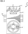
- FIG. 4shows a planar top perspective view of an embodiment of a plasma source
- FIG. 5shows an elevated side perspective view of an embodiment of a plasma source
- FIG. 6shows cross-sectional view of an embodiment of a plasma source
- FIG. 7shows a cross-sectional view of a portion of a passage formed within an embodiment of a plasma source
- FIG. 8shows a cross-section view of a sensor positioned within a sensor receiver proximate to passage wall of a passage formed within an embodiment of a plasma source
- FIG. 9shows an elevated perspective view on an embodiment of a thermal regulating device used within an embodiment of a plasma source
- FIG. 10shows a schematic diagram of an embodiment of a plasma source having a processing control system configured to selectively control the output of the gas source, the plasma source, and/or the processing system;
- FIG. 11shows a graph detailing the correlation between the disassociation fraction measured using a calorimeter system positioned downstream of the embodiment of the plasma source disclosed herein as compared to the temperature measurement technique disclosed in the present application.
- the plasma sourcecomprises a remote plasma source used in semiconductor manufacturing and processing applications.
- the plasma sourcemay comprise any variety of plasma sources used in any variety of applications.
- the plasma source 10may include at least one plasma source body 12 .
- the plasma source body 12includes a first plate or body member 14 and at least a second plate or body member 16 .
- One or more support members or plasma chamber sectionsmay be positioned between the first body member 14 and the second body member 16 . For example, as shown in FIGS.
- a first support member 18 and at least a second support member 20are positioned between the first body member 14 and the second body member 16 of the plasma source body 12 .
- any number of support membersmay be positioned between the first body member 14 and second body member 16 .
- At least one thermal regulating devicemay be affixed to or otherwise coupled to the plasma source body 12 .
- at least one thermal regulating devicemay be configured to actively regulate the temperature of at least a portion of the plasma source body 12 or the various components thereof.
- a first thermal regulating device 100 and at least a second thermal regulation device 104are detachably coupled to the plasma source body 12 .
- any number of thermal regulating devicesmay be used with the plasma source 10 .
- at least one of the thermal regulating devices, 100 , 104may include at least one regulating device body 130 .
- the regulating device body 130may include one or more apertures, ports, or openings formed thereon. More specifically, in the illustrated embodiments the regulating body 130 of the first thermal regulating device 100 and second thermal regulating device 104 includes at least one inlet 106 and at least one outlet 108 formed thereon, although those skilled in the art will appreciate the any number of inlets and/or outlets may be formed on the regulating device body 130 . In one embodiment, the inlet 106 and outlet 108 are configured to permit one or more fluids or materials to be introduced into and/or removed from the regulating device body 130 during use. For example, FIG.
- FIG. 9shows an elevated perspective view of an embodiment of the second thermal regulating device 104 wherein the inlet 106 and outlet 108 are in fluid communication with a regulating device body 130 forming the second thermal regulating device 104 .
- one or more fluids or materialsmay be introduced into and evacuated from the regulating device body 130 via at least one of the inlet 106 and/or outlet 108 .
- the regulating device body 130includes at least one aperture or passage 132 formed therein.
- the regulating device body 130need not include the aperture or passage 132 .
- at least one of the first thermal regulating device 100 and the second thermal regulating device 104may be manufactured from at least one material having a high coefficient of thermal conductivity.
- At least one of the first thermal regulating device 100 and a second thermal regulating device 104may be manufactured from copper, aluminum, various alloys, and the like. Further, at least one of the first thermal regulating device 100 and the second thermal regulating device 104 may include one or more features formed on the regulating device body 130 configured to enhance or increase the surface area of the thermal regulating device 100 , 104 thereby enhancing thermal performance.
- the thermal regulating devices 100 , 104comprise cold plates, chillers, fluid-based cooling devices or similar devices positioned proximate to and in thermal contact with at least a portion of the plasma source body 12 .
- one or more fastener or coupling apertures 110may be formed on at least one of the first thermal regulating device 100 , the second thermal regulating device 104 , or both.
- the coupling apertures 110may be configured to permit at least one of the first thermal regulating device 100 , the second thermal regulating device 104 , or both to be coupled to or otherwise affixed to the plasma source body 12 .
- the coupling apertures 110may be sized and configured to receive one or more fasteners therein.
- at least one thermal regulating device 100 , 104may be coupled to the plasma source body 12 using any variety of devices and methods known in the art, including, without limitations, bolts, screws, friction fit devices, retention devices, welds, and the like.
- one or more electrical devicesmay be coupled to at least one of the thermal regulating devices 100 , 104 , and/or components forming or coupled to the plasma source body 12 .
- a first power source 120 and at least a second power source 122are coupled to or otherwise affixed to the plasma source body 12 proximate to the thermal regulating devices 100 , 104 .
- Exemplary alternate electrical devices or power sourcesinclude, without limitations, RF sources, plasma generators, transformers, capacitors, electromagnets, inductors, sensors, field generation devices, and the like.
- one or more coupling devices or fixtures 112may be used to electrically couple and/or ground at least one of the first power source 120 , second power source, 122 or both to the plasma source body 12 .
- the plasma source 10may include one or more thermal sensors 62 , 66 , 70 (See FIGS. 6-8 ) positioned on or at various locations on the plasma source body 12 .
- the various thermal sensorsmay be in communication with one or more processors or controllers (See FIG. 10 , processing control system 170 ) via one or more sensor conduits (See FIG. 10 , conduit 64 , 68 , 72 ).
- a first sensor conduit 64 , a second sensor conduit 68 , and a third sensor conduit 72are shown coupled to the plasma support body 12 .
- the plasma source 10may include a first sensor 62 and at least a second sensor 66 . A more detailed description of the first sensor 62 , second sensor 66 , and additional optional sensors 70 will be provided in subsequent paragraphs.
- FIGS. 2-6show various features and elements of the plasma source body 12 .
- the plasma source body 12may include one or more support members or plasma chamber sections 18 , 20 positioned between the first body member 14 and the second body member 16 .
- a first support member 18 and a second support member 20are positioned between and in fluid communication with the first body member 14 and second body member 16 , although those skilled in the art will appreciate the any number of support members may be used to form a portion of the plasma source body 12 .
- at least one plasma chamber, region, and/or body blockmay be positioned between any communication with at least one of the first body member 14 , second body member 16 , first support member 18 , and second support member 20 .
- a first plasma chamber 22is coupled to and in fluid communication with the first support member 18 and the second support member 20 .
- the second plasma chamber 24is coupled to and in fluid communication with the first support member 18 and the second support member 20 .
- the first plasma chamber 22 and second plasma chamber 24are orthogonal to the first support member 18 and the second support member 20 , although those skilled in the art will appreciate that at least one of the first plasma chamber 22 and second plasma chamber 24 need not be orthogonal to at least one of the first support member 18 and/or the second support member 20 .
- the plasma source 10comprises a toroidal remote plasma source although those skilled in the art will appreciate that the plasma source body 12 may be formed in any variety of shapes and configurations.
- the various components forming the plasma source body 12including the first body member 14 , second body member 16 , first support member 18 , second support member 20 , first plasma chamber 22 , and the second plasma chamber 24 may be manufactured from any variety of materials including, without limitation, aluminum, stainless steel, copper, various alloys, and the like.
- at least one isolator, gasket, or similar devicemay be positioned between the plasma chambers 22 , 24 and at least one of the first support member 18 and/or the second support member 20 .
- an isolator 26is positioned between the first support member 18 and the first plasma chamber 22 .
- an additional isolator 26is positioned between the first plasma chamber 22 and the second support member 20 .
- an isolator 26may be positioned between the second plasma chamber 24 and the first support member 18 and/or the second support member 20 .
- the passage 40may be formed within the plasma source body 12 .
- the passage 40may be formed from at least one passage or interface surface 86 .
- the passage surface 86may include one or more features or materials applied thereto.
- the passage surface 86 forming the passage 40may include one or more surface treatments or modifications (e.g. anodizing, coatings, micro-structuring, etc.) applied thereto.
- the passage 40may be in communication with one or more inlets, outlets, or similar apertures formed in the various components forming the plasma source body 12 .
- the passage 40is in fluid communication with at least one inlet 30 formed on the first body member 14 and at least one outlet 32 formed on the second body member 16 .
- one or more fluids, gases, or similar materialsmay be introduced into and evacuated from the passage 40 formed in the plasma source body 12 .
- one or more additional access portsmay be formed in the plasma source body 12 in may or may not be in communication with a portion of the passage 40 formed therein.
- at least one access port 50may be formed in the first body member 14 and may be in communication with the passage 40 .
- a second access port 52may be formed in the second body member 16 and may be in communication with the passage 40 .
- the access ports 50 , 52may be sized to receive one or more igniters, sensors, meters, or similar devices therein.
- the passage 40 formed in the plasma source body 12may form multiple pathways.
- the passage 40includes a first pathway 42 and at least a second pathway 44 formed within the plasma source body 12 , although those skilled in the art will appreciate that any number of pathways may be formed within the plasma source body 12 .
- the first pathway 42is formed within the first plasma chamber 22 while the second pathway 44 may be formed within the second plasma chamber 24 .
- a first sensor 62may be positioned within a first sensor receiver 80 formed in the plasma source body 12 . More specifically, in the illustrated embodiment, the first sensor 62 is positioned within the first sensor receiver 80 such that the first sensor 62 is in close proximity to at least one passage surface 86 formed within or proximate to the passage 40 formed within the plasma source body 12 .
- the passage surface 86may comprise at least one optical window, sensor window, where the like.
- at least a second sensor 66may be positioned within at least a second sensor receiver 82 formed within the plasma source body 12 .
- the second sensor receiver 82may be positioned proximate to the outlet 32 of the plasma source body 12 . In another embodiment, the second sensor receiver 82 need not be positioned proximate to the outlet 32 .
- the second sensor 66may be positioned in close proximity to at least one passage surface 86 formed within or proximate to the passage 40 formed within the plasma source body 12 .
- at least one optional sensor 70may be positioned within at least an optional sensor receiver 84 formed within the plasma source body 12 .
- At least one of the first sensor 62 , second sensor 66 , and optional sensor 70comprises a thermal sensor configured to measure the temperature of the passage surface 86 of the passage 40 , the first pathway 42 , and second pathway 44 , and the outlet 32 at one or more locations within the plasma source body 12 , although those skilled in the art will appreciate that any variety of sensors may be used. Exemplary alternate sensors include, without limitations, optical sensors, flow sensors, and the like. Optionally, any variety of thermal sensors may be used with the plasma source 10 , including, without limitations, thermocouples, thermopiles, thermisters, resistance thermometers, silicon bandgap temperature sensors, and the like. For example, in the illustrated embodiment, the first sensor 62 is located distally from the second sensor 66 .
- the first sensor 62is located proximate to the first plasma chamber 22 and may in communication with the passage 40 formed in the plasma source body 12 thereby permitting the first sensor 62 to measure a first temperature (T 1 ) of the passage surface 86 of the passage 40 formed in the plasma source body 12 at a first location, for example, proximate to the plasma region 124 .
- the second sensor 66is located proximate to the outlet 32 and may be configured to measure a second temperature (T 2 ) of the passage surface 86 of the passage 40 formed in the plasma source body 12 at a second location. As shown, in the illustrated embodiments, the second temperature (T 2 ) of the passage surface 86 of the passage 40 is measured proximate to the outlet 32 .
- any number of temperatures (T n ) of the passage surface 86may be measured at any variety of locations within the passage 40 using any number of optional sensors 70 positioned on the plasma source body 12 .
- the usermay calculate at least one temperature gradient between T 1 , T 2 , and/or T n (if present).
- the present applicationfurther discloses a method of detecting variations in the output of radicals generated by at least one plasma source.
- the plasma source 10 disclosed in FIGS. 1-9may be used to detect variations in the radical output from a remote plasma source.
- the plasma source 10 disclosed in the present applicationmay be configured to provide a diagnostic method of monitoring changing gas and surface conditions within the passage 40 formed within the plasma source body 12 .
- at least one processing gas 90may be directed from at least one gas inlet 30 into the passage 40 formed within the plasma source body 12 to form at least one input gas 92 .
- the processing gas 90comprises hydrogen (H2), although any variety of alternate gases may be used but the present system.
- Exemplary alternate gasesinclude, without limitations, fluorine-based gases (e.g. NF 3 ), oxygen (O 2 ), nitrogen (N 2 ), and the like.
- the processing gas 90 /input gas 92may be directed into and evacuated from the plasma source body 12 by one or more pumps (not shown) and directed to flow through the first pathway 42 and second pathway 44 formed in the passage 40 .
- At least one power supply(not shown) may be coupled to the plasma source 10 to create at least one plasma in at least one plasma chamber 22 , 24 .
- the input gas 92 flowing through the first plasma chamber 22 and second plasma chamber 24interacts with the plasma thereby energizing the input gas 92 to form at least one plasma region 124 within the passage 40 .
- At least a portion of the input gas 92 flowing through the plasma region 124is subjected to the plasma formed within the plasma region 124 and produces at least one reactive or disassociated gas 94 within at least a portion of the passage 40 . Thereafter, the input gas 92 /disassociated gas 94 may be evacuated from the plasma source 10 via the outlet 32 . More specifically, as the input gas 92 is activated by the plasma along the passage 40 in the plasma source 10 , a portion of the input gas 92 is disassociated in the plasma region 124 to form the disassociated gas 94 . A portion of the disassociated gas 94 may recombine along the passage surface 86 of the passage 40 proximate to the first sensor 62 .
- the first sensor 62which, in the illustrated embodiments, is positioned proximate to at least one of the first plasma chamber 22 in the second plasma chamber 24 may be configured to measure a first temperature (T 1 ) of the passage surface 86 within the passage 40 of the plasma source body 12 distally from the outlet 32 .
- the first sensor 62is configured to measure the temperature of the passage surface 86 at a location within or proximate to the plasma region 124 .
- the first temperature T 1may reflect a temperature associate with recombination of the disassociated gas 94 at or proximate to the passage surface 86 of the passage 40 proximate to the first sensor 62 .
- the second sensor 66 positioned proximate to the outlet 32 of the passage 40may be configured to measure at least a second temperature (T 2 ) of the passage surface 86 at a different location than the first sensor 62 .
- the second sensor 66is configured to measure the temperature of the passage surface 86 proximate to the output 96 .
- the second sensor 66is positioned outside of the plasma region 124 . As a result, a portion of the disassociated gas 94 may re-disassociate within the plasma region 124 , thereby resulting a temperature variation (T 2 ) measured at the passage surface 86 by the second sensor 66 located proximate to the outlet 32 .
- the radical output of the plasma source 10may be quickly (virtually immediately) and easily monitored by comparing the temperature differences between the first temperature T 1 measured by the first sensor 62 and the second temperature T 2 measured by the second sensor 66 .
- at least one optional sensor 70may be positioned anywhere within the proximate to the passage 40 and may be configured to measure any number of additional temperatures (T n ) of the passage surface 86 at any desired location within the passage 40 . Thereafter, as shown in FIGS. 6 and 10 , the temperature data measured by the first sensor 62 , second sensor 66 , and optional sensor 70 may be provided to at least one processing control system 170 via the first sensor conduit 64 , the second sensor conduit 68 , and the optional sensor conduit 72 .
- the processing control system 170may be configured to receive data from at least one of the gas source 150 , the plasma source 10 , and/or the processing system 160 . Further, the processing control system 170 may be configured to provide data and or control commands 172 , 174 , 176 to at least one of the gas source 150 , plasma source 10 , and/or the processing system 160 thereby permitting the processing control system 170 actively control at least one of the gas source 150 , the plasma source 10 , and/or the processing system 160 . In one embodiment, the processing control system 170 may be configured to correlate and approximate the temperature of the passage surface 86 to the temperature of the reactive gas 94 flowing within the passage 40 at various locations.
- the processing control system 170may be configured to estimate the radical output generated by permitting the user to more accurately determine radical losses and/or radical recombination effects within or proximate to the first plasma chamber 22 , the second plasma chamber 24 , and/or various other locations with in plasma source body 12 by comparing the temperatures T 1 and T n to the temperature T 2 measured by the second sensor 66 positioned proximate to the outlet 32 .
- the processing control system 170may be configured to permit the user to actively monitor and control the gas source 150 , plasma source 10 , and/or the processing system 160 to maintain a consistent reactive gas flow to the processing system 160 .
- FIG. 11shows graphically the correlation between the disassociation fraction (normalized) measured using a calorimeter downstream of the plasma source 10 as compared to the T 1 and T 2 measurement technique described herein. More specifically, the disassociation fraction shown in FIG. 11 is calculated based on calorimeter power measurement and shows the reactive output from the plasma source 10 (see FIG. 1 ). As shown, the radical output from the plasma source 10 can be accurately determined by using the T 1 and T 2 measurement technique described herein.
Landscapes
- Physics & Mathematics (AREA)
- Engineering & Computer Science (AREA)
- Plasma & Fusion (AREA)
- Chemical & Material Sciences (AREA)
- Analytical Chemistry (AREA)
- Spectroscopy & Molecular Physics (AREA)
- Plasma Technology (AREA)
- Drying Of Semiconductors (AREA)
- Physical Vapour Deposition (AREA)
- Investigating, Analyzing Materials By Fluorescence Or Luminescence (AREA)
Abstract
Description
Claims (20)
Priority Applications (1)
| Application Number | Priority Date | Filing Date | Title |
|---|---|---|---|
| US16/438,827US11114287B2 (en) | 2018-06-14 | 2019-06-12 | Radical output monitor for a remote plasma source and method of use |
Applications Claiming Priority (2)
| Application Number | Priority Date | Filing Date | Title |
|---|---|---|---|
| US201862684820P | 2018-06-14 | 2018-06-14 | |
| US16/438,827US11114287B2 (en) | 2018-06-14 | 2019-06-12 | Radical output monitor for a remote plasma source and method of use |
Publications (2)
| Publication Number | Publication Date |
|---|---|
| US20190385829A1 US20190385829A1 (en) | 2019-12-19 |
| US11114287B2true US11114287B2 (en) | 2021-09-07 |
Family
ID=68840258
Family Applications (1)
| Application Number | Title | Priority Date | Filing Date |
|---|---|---|---|
| US16/438,827Active2039-12-02US11114287B2 (en) | 2018-06-14 | 2019-06-12 | Radical output monitor for a remote plasma source and method of use |
Country Status (8)
| Country | Link |
|---|---|
| US (1) | US11114287B2 (en) |
| EP (1) | EP3785494A4 (en) |
| JP (1) | JP7301075B2 (en) |
| KR (1) | KR102697703B1 (en) |
| CN (1) | CN112335342B (en) |
| SG (1) | SG11202011069RA (en) |
| TW (1) | TWI809122B (en) |
| WO (1) | WO2019241405A1 (en) |
Cited By (5)
| Publication number | Priority date | Publication date | Assignee | Title |
|---|---|---|---|---|
| US11569070B2 (en) | 2017-06-27 | 2023-01-31 | Canon Anelva Corporation | Plasma processing apparatus |
| US11600466B2 (en)* | 2018-06-26 | 2023-03-07 | Canon Anelva Corporation | Plasma processing apparatus, plasma processing method, and memory medium |
| US11600469B2 (en) | 2017-06-27 | 2023-03-07 | Canon Anelva Corporation | Plasma processing apparatus |
| US11626270B2 (en) | 2017-06-27 | 2023-04-11 | Canon Anelva Corporation | Plasma processing apparatus |
| US11961710B2 (en) | 2017-06-27 | 2024-04-16 | Canon Anelva Corporation | Plasma processing apparatus |
Families Citing this family (1)
| Publication number | Priority date | Publication date | Assignee | Title |
|---|---|---|---|---|
| CN115900990A (en)* | 2023-01-03 | 2023-04-04 | 大连理工大学 | Temperature monitoring system for seven-channel cascaded arc plasma source |
Citations (61)
| Publication number | Priority date | Publication date | Assignee | Title |
|---|---|---|---|---|
| EP0520519A1 (en) | 1991-06-27 | 1992-12-30 | Applied Materials, Inc. | Plasma processing reactor and process for plasma etching |
| US5349154A (en) | 1991-10-16 | 1994-09-20 | Rockwell International Corporation | Diamond growth by microwave generated plasma flame |
| US5429070A (en) | 1989-06-13 | 1995-07-04 | Plasma & Materials Technologies, Inc. | High density plasma deposition and etching apparatus |
| JPH07254496A (en) | 1994-03-17 | 1995-10-03 | Fuji Electric Co Ltd | Induction plasma generator |
| US5478608A (en) | 1994-11-14 | 1995-12-26 | Gorokhovsky; Vladimir I. | Arc assisted CVD coating method and apparatus |
| US5587207A (en) | 1994-11-14 | 1996-12-24 | Gorokhovsky; Vladimir I. | Arc assisted CVD coating and sintering method |
| JPH0955372A (en) | 1995-08-11 | 1997-02-25 | Nippon Steel Corp | Plasma processing device |
| EP0376546B1 (en) | 1988-12-28 | 1999-03-10 | AT&T Corp. | Processes depending on plasma generation |
| KR100231221B1 (en) | 1991-02-04 | 1999-11-15 | 플라즈마 앤드 머티리얼즈 테크놀러지즈 인코포레이티드 | High density plasma depositoon and etching apparatus |
| US6043608A (en) | 1996-10-31 | 2000-03-28 | Nec Corporation | Plasma processing apparatus |
| US6150628A (en) | 1997-06-26 | 2000-11-21 | Applied Science And Technology, Inc. | Toroidal low-field reactive gas source |
| US20020008480A1 (en) | 2000-06-06 | 2002-01-24 | Matsushita Electric Works, Ltd. | Plasma treatment apparatus and plasma treatment method |
| US6352049B1 (en) | 1998-02-09 | 2002-03-05 | Applied Materials, Inc. | Plasma assisted processing chamber with separate control of species density |
| US20020046991A1 (en) | 1997-06-26 | 2002-04-25 | Smith Donald K. | Toroidal low-field reactive gas source |
| US6418874B1 (en) | 2000-05-25 | 2002-07-16 | Applied Materials, Inc. | Toroidal plasma source for plasma processing |
| US6422172B1 (en) | 1997-03-19 | 2002-07-23 | Hitachi, Ltd. | Plasma processing apparatus and plasma processing method |
| US6432260B1 (en) | 1999-08-06 | 2002-08-13 | Advanced Energy Industries, Inc. | Inductively coupled ring-plasma source apparatus for processing gases and materials and method thereof |
| JP3381916B2 (en) | 1990-01-04 | 2003-03-04 | マトソン テクノロジー,インコーポレイテッド | Low frequency induction type high frequency plasma reactor |
| EP0884760B1 (en) | 1997-06-11 | 2003-03-19 | Kawasaki Jukogyo Kabushiki Kaisha | Electron-beam excited plasma generator |
| US20030079686A1 (en) | 2001-10-26 | 2003-05-01 | Ling Chen | Gas delivery apparatus and method for atomic layer deposition |
| RU2209532C2 (en) | 2001-10-10 | 2003-07-27 | Сорокин Игорь Борисович | Plasma accelerator with closed electron drift |
| US6635578B1 (en) | 1998-02-09 | 2003-10-21 | Applied Materials, Inc | Method of operating a dual chamber reactor with neutral density decoupled from ion density |
| US6679981B1 (en) | 2000-05-11 | 2004-01-20 | Applied Materials, Inc. | Inductive plasma loop enhancing magnetron sputtering |
| JP2004047192A (en) | 2002-07-10 | 2004-02-12 | Adtec Plasma Technology Co Ltd | Transformer discharge type plasma generator with permeable core |
| WO2004023853A1 (en) | 2002-09-05 | 2004-03-18 | Seppo Konkola | Method and equipment for generating a gas plasma ball |
| KR20040079559A (en) | 2003-03-07 | 2004-09-16 | 위순임 | Vacuum process chamber remote plasma generator |
| US20040206730A1 (en) | 2003-04-16 | 2004-10-21 | Applied Science & Technology | Toroidal low-field reactive gas and plasma source having a dielectric vacuum vessel |
| US20050000655A1 (en) | 2003-05-07 | 2005-01-06 | Soon-Im Wi | Inductive plasma chamber having multi discharge tube bridge |
| US6855906B2 (en) | 2001-10-16 | 2005-02-15 | Adam Alexander Brailove | Induction plasma reactor |
| US20050100669A1 (en) | 2003-11-12 | 2005-05-12 | Veeco Instruments, Inc. | Method and apparatus for fabricating a conformal thin film on a substrate |
| US20050276928A1 (en) | 2003-02-03 | 2005-12-15 | Octec Inc. | Plasma processing apparatus, electrode plate for plasma processing apparatus, and electrode plate manufacturing method |
| WO2006037991A2 (en) | 2004-10-04 | 2006-04-13 | C-Tech Innovation Limited | Microwave plasma apparatus with vorticular gas flow |
| US20060118240A1 (en) | 2004-12-03 | 2006-06-08 | Applied Science And Technology, Inc. | Methods and apparatus for downstream dissociation of gases |
| US20060197037A1 (en) | 2004-12-20 | 2006-09-07 | Purser Kenneth H | Beam neutralization in low-energy high-current ribbon-beam implanters |
| US20070012563A1 (en) | 2005-07-15 | 2007-01-18 | Soon-Im Wi | Multi chamber plasma process system |
| US20070015360A1 (en) | 2005-07-18 | 2007-01-18 | Applied Materials, Inc. | Contact clean by remote plasma and repair of silicide surface |
| US20070079935A1 (en) | 2003-04-16 | 2007-04-12 | Mks Instruments, Inc. | Applicators and cooling systems for a plasma device |
| US20070119370A1 (en) | 2005-11-04 | 2007-05-31 | Paul Ma | Apparatus and process for plasma-enhanced atomic layer deposition |
| US7268084B2 (en) | 2004-09-30 | 2007-09-11 | Tokyo Electron Limited | Method for treating a substrate |
| US20070245962A1 (en) | 2006-04-21 | 2007-10-25 | Dae-Kyu Choi | Plasma Processing System and Method of Contolling the Same |
| US20070245963A1 (en) | 2006-04-24 | 2007-10-25 | Dae-Kyu Choi | Inductively Coupled Plasma Reactor with Multiple Magnetic Cores |
| US20100055347A1 (en)* | 2008-08-29 | 2010-03-04 | Tokyo Electron Limited | Activated gas injector, film deposition apparatus, and film deposition method |
| US7861668B2 (en) | 2002-01-10 | 2011-01-04 | Hitachi Kokusai Electric Inc. | Batch-type remote plasma processing apparatus |
| JP2011086564A (en) | 2009-10-19 | 2011-04-28 | Ulvac Japan Ltd | Analyzing device |
| WO2011024174A9 (en) | 2009-08-27 | 2011-10-20 | Mosaic Crystals Ltd. | Penetrating plasma generating apparatus for high vacuum chambers |
| JP4861329B2 (en) | 2004-09-30 | 2012-01-25 | 東京エレクトロン株式会社 | Plasma processing system for processing substrates |
| JP2012094399A (en) | 2010-10-27 | 2012-05-17 | Ulvac Japan Ltd | Radical measurement apparatus and radical measurement pipe |
| US20130118589A1 (en) | 2011-11-15 | 2013-05-16 | Mks Instruments, Inc. | Toroidal Plasma Channel with Varying Cross-Section Areas Along the Channel |
| WO2014007472A1 (en) | 2012-07-03 | 2014-01-09 | Plasmart Inc. | Plasma generation apparatus and plasma generation method |
| EP2394496B1 (en) | 2009-02-04 | 2014-04-02 | General Fusion, Inc. | Systems and methods for compressing plasma |
| KR101488538B1 (en) | 2006-07-18 | 2015-02-02 | 램 리써치 코포레이션 | Hybrid rf capacitively and inductively coupled plasma source using multifrequency rf powers and methods of use thereof |
| US9035553B2 (en) | 2011-11-09 | 2015-05-19 | Dae-Kyu Choi | Hybrid plasma reactor |
| US20150279631A1 (en) | 2011-01-25 | 2015-10-01 | Advanced Energy Industries, Inc. | Electrostatic remote plasma source system and method |
| US20150318148A1 (en)* | 2014-03-27 | 2015-11-05 | Mks Instruments, Inc. | Microwave plasma applicator with improved power uniformity |
| US9275839B2 (en) | 2007-10-19 | 2016-03-01 | Mks Instruments, Inc. | Toroidal plasma chamber for high gas flow rate process |
| US20160077508A1 (en) | 2014-09-12 | 2016-03-17 | Applied Materials, Inc. | Controller for treatment of semiconductor processing equipment effluent |
| WO2016141464A1 (en) | 2015-03-11 | 2016-09-15 | General Fusion Inc. | Modular compression chamber |
| US20160307739A1 (en) | 2015-04-14 | 2016-10-20 | Dandan Co., Ltd. | Remote plasma generator using ceramic |
| KR20160129304A (en) | 2015-04-30 | 2016-11-09 | 최대규 | Cooling kit and a plasma reactor having the same magnetic core for cooling |
| US20190006154A1 (en) | 2017-06-28 | 2019-01-03 | Chaolin Hu | Toroidal Plasma Chamber |
| US20190048770A1 (en)* | 2017-08-11 | 2019-02-14 | GM Global Technology Operations LLC | Non-thermal plasma/ozone-assisted catalytic system and use in exhaust systems |
Family Cites Families (13)
| Publication number | Priority date | Publication date | Assignee | Title |
|---|---|---|---|---|
| US6024826A (en)* | 1996-05-13 | 2000-02-15 | Applied Materials, Inc. | Plasma reactor with heated source of a polymer-hardening precursor material |
| US6815633B1 (en) | 1997-06-26 | 2004-11-09 | Applied Science & Technology, Inc. | Inductively-coupled toroidal plasma source |
| US5937541A (en)* | 1997-09-15 | 1999-08-17 | Siemens Aktiengesellschaft | Semiconductor wafer temperature measurement and control thereof using gas temperature measurement |
| US6450116B1 (en)* | 1999-04-22 | 2002-09-17 | Applied Materials, Inc. | Apparatus for exposing a substrate to plasma radicals |
| JP2001274148A (en)* | 2000-03-24 | 2001-10-05 | Tokyo Electron Ltd | System and method for plasma processing |
| EP1156511A1 (en)* | 2000-05-19 | 2001-11-21 | Applied Materials, Inc. | Remote plasma CVD apparatus |
| US6902646B2 (en) | 2003-08-14 | 2005-06-07 | Advanced Energy Industries, Inc. | Sensor array for measuring plasma characteristics in plasma processing environments |
| CN101466445A (en)* | 2006-06-12 | 2009-06-24 | 山米奎普公司 | Vapor delivery to devices under vacuum |
| US9190289B2 (en)* | 2010-02-26 | 2015-11-17 | Lam Research Corporation | System, method and apparatus for plasma etch having independent control of ion generation and dissociation of process gas |
| TW201325326A (en)* | 2011-10-05 | 2013-06-16 | Applied Materials Inc | Plasma processing equipment and substrate support assembly thereof |
| US10316409B2 (en)* | 2012-12-21 | 2019-06-11 | Novellus Systems, Inc. | Radical source design for remote plasma atomic layer deposition |
| WO2017189194A1 (en)* | 2016-04-26 | 2017-11-02 | Applied Materials, Inc. | Temperature controlled remote plasma clean for exhaust deposit removal |
| US11837479B2 (en)* | 2016-05-05 | 2023-12-05 | Applied Materials, Inc. | Advanced temperature control for wafer carrier in plasma processing chamber |
- 2019
- 2019-06-12EPEP19818618.1Apatent/EP3785494A4/enactivePending
- 2019-06-12KRKR1020217001013Apatent/KR102697703B1/enactiveActive
- 2019-06-12CNCN201980038899.7Apatent/CN112335342B/enactiveActive
- 2019-06-12WOPCT/US2019/036796patent/WO2019241405A1/ennot_activeCeased
- 2019-06-12SGSG11202011069RApatent/SG11202011069RA/enunknown
- 2019-06-12USUS16/438,827patent/US11114287B2/enactiveActive
- 2019-06-12JPJP2020568979Apatent/JP7301075B2/enactiveActive
- 2019-06-13TWTW108120410Apatent/TWI809122B/enactive
Patent Citations (65)
| Publication number | Priority date | Publication date | Assignee | Title |
|---|---|---|---|---|
| EP0376546B1 (en) | 1988-12-28 | 1999-03-10 | AT&T Corp. | Processes depending on plasma generation |
| US5429070A (en) | 1989-06-13 | 1995-07-04 | Plasma & Materials Technologies, Inc. | High density plasma deposition and etching apparatus |
| JP3381916B2 (en) | 1990-01-04 | 2003-03-04 | マトソン テクノロジー,インコーポレイテッド | Low frequency induction type high frequency plasma reactor |
| KR100231221B1 (en) | 1991-02-04 | 1999-11-15 | 플라즈마 앤드 머티리얼즈 테크놀러지즈 인코포레이티드 | High density plasma depositoon and etching apparatus |
| EP0520519A1 (en) | 1991-06-27 | 1992-12-30 | Applied Materials, Inc. | Plasma processing reactor and process for plasma etching |
| US5349154A (en) | 1991-10-16 | 1994-09-20 | Rockwell International Corporation | Diamond growth by microwave generated plasma flame |
| JPH07254496A (en) | 1994-03-17 | 1995-10-03 | Fuji Electric Co Ltd | Induction plasma generator |
| US5478608A (en) | 1994-11-14 | 1995-12-26 | Gorokhovsky; Vladimir I. | Arc assisted CVD coating method and apparatus |
| US5587207A (en) | 1994-11-14 | 1996-12-24 | Gorokhovsky; Vladimir I. | Arc assisted CVD coating and sintering method |
| JPH0955372A (en) | 1995-08-11 | 1997-02-25 | Nippon Steel Corp | Plasma processing device |
| US6043608A (en) | 1996-10-31 | 2000-03-28 | Nec Corporation | Plasma processing apparatus |
| US6422172B1 (en) | 1997-03-19 | 2002-07-23 | Hitachi, Ltd. | Plasma processing apparatus and plasma processing method |
| EP0884760B1 (en) | 1997-06-11 | 2003-03-19 | Kawasaki Jukogyo Kabushiki Kaisha | Electron-beam excited plasma generator |
| US20020046991A1 (en) | 1997-06-26 | 2002-04-25 | Smith Donald K. | Toroidal low-field reactive gas source |
| US6150628A (en) | 1997-06-26 | 2000-11-21 | Applied Science And Technology, Inc. | Toroidal low-field reactive gas source |
| US6635578B1 (en) | 1998-02-09 | 2003-10-21 | Applied Materials, Inc | Method of operating a dual chamber reactor with neutral density decoupled from ion density |
| US6352049B1 (en) | 1998-02-09 | 2002-03-05 | Applied Materials, Inc. | Plasma assisted processing chamber with separate control of species density |
| US6432260B1 (en) | 1999-08-06 | 2002-08-13 | Advanced Energy Industries, Inc. | Inductively coupled ring-plasma source apparatus for processing gases and materials and method thereof |
| US6679981B1 (en) | 2000-05-11 | 2004-01-20 | Applied Materials, Inc. | Inductive plasma loop enhancing magnetron sputtering |
| US6418874B1 (en) | 2000-05-25 | 2002-07-16 | Applied Materials, Inc. | Toroidal plasma source for plasma processing |
| US20020008480A1 (en) | 2000-06-06 | 2002-01-24 | Matsushita Electric Works, Ltd. | Plasma treatment apparatus and plasma treatment method |
| RU2209532C2 (en) | 2001-10-10 | 2003-07-27 | Сорокин Игорь Борисович | Plasma accelerator with closed electron drift |
| US6855906B2 (en) | 2001-10-16 | 2005-02-15 | Adam Alexander Brailove | Induction plasma reactor |
| US20030079686A1 (en) | 2001-10-26 | 2003-05-01 | Ling Chen | Gas delivery apparatus and method for atomic layer deposition |
| US20070003698A1 (en) | 2001-10-26 | 2007-01-04 | Ling Chen | Enhanced copper growth with ultrathin barrier layer for high performance interconnects |
| US7861668B2 (en) | 2002-01-10 | 2011-01-04 | Hitachi Kokusai Electric Inc. | Batch-type remote plasma processing apparatus |
| JP2004047192A (en) | 2002-07-10 | 2004-02-12 | Adtec Plasma Technology Co Ltd | Transformer discharge type plasma generator with permeable core |
| WO2004023853A1 (en) | 2002-09-05 | 2004-03-18 | Seppo Konkola | Method and equipment for generating a gas plasma ball |
| US20050276928A1 (en) | 2003-02-03 | 2005-12-15 | Octec Inc. | Plasma processing apparatus, electrode plate for plasma processing apparatus, and electrode plate manufacturing method |
| KR20040079559A (en) | 2003-03-07 | 2004-09-16 | 위순임 | Vacuum process chamber remote plasma generator |
| EP2296166B1 (en) | 2003-04-16 | 2014-01-08 | MKS Instruments, Inc. | Plasma apparatus comprising a heat sink |
| US20040206730A1 (en) | 2003-04-16 | 2004-10-21 | Applied Science & Technology | Toroidal low-field reactive gas and plasma source having a dielectric vacuum vessel |
| US20070079935A1 (en) | 2003-04-16 | 2007-04-12 | Mks Instruments, Inc. | Applicators and cooling systems for a plasma device |
| US20050000655A1 (en) | 2003-05-07 | 2005-01-06 | Soon-Im Wi | Inductive plasma chamber having multi discharge tube bridge |
| US20050100669A1 (en) | 2003-11-12 | 2005-05-12 | Veeco Instruments, Inc. | Method and apparatus for fabricating a conformal thin film on a substrate |
| JP4861329B2 (en) | 2004-09-30 | 2012-01-25 | 東京エレクトロン株式会社 | Plasma processing system for processing substrates |
| US7268084B2 (en) | 2004-09-30 | 2007-09-11 | Tokyo Electron Limited | Method for treating a substrate |
| WO2006037991A2 (en) | 2004-10-04 | 2006-04-13 | C-Tech Innovation Limited | Microwave plasma apparatus with vorticular gas flow |
| US20070274893A1 (en) | 2004-10-04 | 2007-11-29 | C-Tech Innovation Limited | Microwave Plasma Apparatus |
| US20060118240A1 (en) | 2004-12-03 | 2006-06-08 | Applied Science And Technology, Inc. | Methods and apparatus for downstream dissociation of gases |
| US20060197037A1 (en) | 2004-12-20 | 2006-09-07 | Purser Kenneth H | Beam neutralization in low-energy high-current ribbon-beam implanters |
| US20070012563A1 (en) | 2005-07-15 | 2007-01-18 | Soon-Im Wi | Multi chamber plasma process system |
| US7550381B2 (en) | 2005-07-18 | 2009-06-23 | Applied Materials, Inc. | Contact clean by remote plasma and repair of silicide surface |
| US20070015360A1 (en) | 2005-07-18 | 2007-01-18 | Applied Materials, Inc. | Contact clean by remote plasma and repair of silicide surface |
| US20070119370A1 (en) | 2005-11-04 | 2007-05-31 | Paul Ma | Apparatus and process for plasma-enhanced atomic layer deposition |
| US20070245962A1 (en) | 2006-04-21 | 2007-10-25 | Dae-Kyu Choi | Plasma Processing System and Method of Contolling the Same |
| US20070245963A1 (en) | 2006-04-24 | 2007-10-25 | Dae-Kyu Choi | Inductively Coupled Plasma Reactor with Multiple Magnetic Cores |
| KR101488538B1 (en) | 2006-07-18 | 2015-02-02 | 램 리써치 코포레이션 | Hybrid rf capacitively and inductively coupled plasma source using multifrequency rf powers and methods of use thereof |
| US9275839B2 (en) | 2007-10-19 | 2016-03-01 | Mks Instruments, Inc. | Toroidal plasma chamber for high gas flow rate process |
| US20100055347A1 (en)* | 2008-08-29 | 2010-03-04 | Tokyo Electron Limited | Activated gas injector, film deposition apparatus, and film deposition method |
| EP2394496B1 (en) | 2009-02-04 | 2014-04-02 | General Fusion, Inc. | Systems and methods for compressing plasma |
| WO2011024174A9 (en) | 2009-08-27 | 2011-10-20 | Mosaic Crystals Ltd. | Penetrating plasma generating apparatus for high vacuum chambers |
| JP2011086564A (en) | 2009-10-19 | 2011-04-28 | Ulvac Japan Ltd | Analyzing device |
| JP2012094399A (en) | 2010-10-27 | 2012-05-17 | Ulvac Japan Ltd | Radical measurement apparatus and radical measurement pipe |
| US20150279631A1 (en) | 2011-01-25 | 2015-10-01 | Advanced Energy Industries, Inc. | Electrostatic remote plasma source system and method |
| US9035553B2 (en) | 2011-11-09 | 2015-05-19 | Dae-Kyu Choi | Hybrid plasma reactor |
| US20130118589A1 (en) | 2011-11-15 | 2013-05-16 | Mks Instruments, Inc. | Toroidal Plasma Channel with Varying Cross-Section Areas Along the Channel |
| WO2014007472A1 (en) | 2012-07-03 | 2014-01-09 | Plasmart Inc. | Plasma generation apparatus and plasma generation method |
| US20150318148A1 (en)* | 2014-03-27 | 2015-11-05 | Mks Instruments, Inc. | Microwave plasma applicator with improved power uniformity |
| US20160077508A1 (en) | 2014-09-12 | 2016-03-17 | Applied Materials, Inc. | Controller for treatment of semiconductor processing equipment effluent |
| WO2016141464A1 (en) | 2015-03-11 | 2016-09-15 | General Fusion Inc. | Modular compression chamber |
| US20160307739A1 (en) | 2015-04-14 | 2016-10-20 | Dandan Co., Ltd. | Remote plasma generator using ceramic |
| KR20160129304A (en) | 2015-04-30 | 2016-11-09 | 최대규 | Cooling kit and a plasma reactor having the same magnetic core for cooling |
| US20190006154A1 (en) | 2017-06-28 | 2019-01-03 | Chaolin Hu | Toroidal Plasma Chamber |
| US20190048770A1 (en)* | 2017-08-11 | 2019-02-14 | GM Global Technology Operations LLC | Non-thermal plasma/ozone-assisted catalytic system and use in exhaust systems |
Non-Patent Citations (3)
| Title |
|---|
| International Search Report dated Jul. 8, 2008 to the PCT Application No. PCT/US2007/081875, 2 pages. |
| The International Search Report dated Sep. 30, 2019 to the PCT Application No. PCT/US2019/036796, 2 pages. |
| The written opinion dated Sep. 30, 2019 to the PCT Application No. PCT/US2019/036796, 2 pages. |
Cited By (7)
| Publication number | Priority date | Publication date | Assignee | Title |
|---|---|---|---|---|
| US11569070B2 (en) | 2017-06-27 | 2023-01-31 | Canon Anelva Corporation | Plasma processing apparatus |
| US11600469B2 (en) | 2017-06-27 | 2023-03-07 | Canon Anelva Corporation | Plasma processing apparatus |
| US11626270B2 (en) | 2017-06-27 | 2023-04-11 | Canon Anelva Corporation | Plasma processing apparatus |
| US11756773B2 (en) | 2017-06-27 | 2023-09-12 | Canon Anelva Corporation | Plasma processing apparatus |
| US11784030B2 (en) | 2017-06-27 | 2023-10-10 | Canon Anelva Corporation | Plasma processing apparatus |
| US11961710B2 (en) | 2017-06-27 | 2024-04-16 | Canon Anelva Corporation | Plasma processing apparatus |
| US11600466B2 (en)* | 2018-06-26 | 2023-03-07 | Canon Anelva Corporation | Plasma processing apparatus, plasma processing method, and memory medium |
Also Published As
| Publication number | Publication date |
|---|---|
| SG11202011069RA (en) | 2020-12-30 |
| KR102697703B1 (en) | 2024-08-23 |
| US20190385829A1 (en) | 2019-12-19 |
| EP3785494A1 (en) | 2021-03-03 |
| TW202017074A (en) | 2020-05-01 |
| EP3785494A4 (en) | 2022-01-26 |
| CN112335342B (en) | 2023-07-14 |
| TWI809122B (en) | 2023-07-21 |
| JP2021530076A (en) | 2021-11-04 |
| JP7301075B2 (en) | 2023-06-30 |
| WO2019241405A1 (en) | 2019-12-19 |
| CN112335342A (en) | 2021-02-05 |
| KR20210009428A (en) | 2021-01-26 |
Similar Documents
| Publication | Publication Date | Title |
|---|---|---|
| US11114287B2 (en) | Radical output monitor for a remote plasma source and method of use | |
| Zhao et al. | Experimental investigation of surface temperature non-uniformity in spray cooling | |
| US8772682B2 (en) | Methods and apparatus for controlling temperature of a multi-zone heater in a process chamber | |
| CN201343570Y (en) | Temperature control spray header | |
| KR101302750B1 (en) | Apparatus for evaluating a thermoelectric device | |
| TW201243955A (en) | Apparatus for monitoring and controlling substrate temperature | |
| US11390951B2 (en) | Fluid control device | |
| JP2014153168A (en) | Emissivity measuring apparatus and emissivity measuring method | |
| KR101744847B1 (en) | Plasuma processing device | |
| JP2014149158A (en) | Device and method for controlling heating of test piece to be heated | |
| US10627050B1 (en) | Cryogenic heating system | |
| KR102771310B1 (en) | pressure control device | |
| US8002463B2 (en) | Method and device for determining the temperature of a substrate | |
| Arpino et al. | Design of a calibration system for heat flux meters | |
| JP7426915B2 (en) | Plasma processing equipment, thermal resistance derivation method, and thermal resistance derivation program | |
| JP4829833B2 (en) | Temperature estimation method and temperature estimation device | |
| Zhang et al. | Design of a cooling system for high density integrated phased array antenna test | |
| CN108828007A (en) | A kind of annular face contacts surface interface contact conductane measuring device | |
| Grosshandler et al. | Development of a high flux conduction calibration apparatus | |
| CN110571118A (en) | Method for determining flow threshold, control device and semiconductor processing equipment | |
| US20250293069A1 (en) | Modeling substrate temperatures | |
| Filtz et al. | New vacuum blackbody cavity for heat flux meter calibration | |
| Nikolaenko et al. | Experimental Investigation of the Contact Heat Resistance in the Threaded Joint Zone of Contact Surfaces | |
| Ribeiro et al. | CONSTRUCTAL DESIGN OF A NON-INVASIVE TEMPERATURE BASED MASS FLOW RATE SENSOR FOR ALGAE PHOTOBIOREACTORS | |
| Kim et al. | Temperature effect on the radiation-corrective gas temperature measurement |
Legal Events
| Date | Code | Title | Description |
|---|---|---|---|
| FEPP | Fee payment procedure | Free format text:ENTITY STATUS SET TO UNDISCOUNTED (ORIGINAL EVENT CODE: BIG.); ENTITY STATUS OF PATENT OWNER: LARGE ENTITY | |
| STPP | Information on status: patent application and granting procedure in general | Free format text:APPLICATION DISPATCHED FROM PREEXAM, NOT YET DOCKETED | |
| AS | Assignment | Owner name:BARCLAYS BANK PLC, NEW YORK Free format text:PATENT SECURITY AGREEMENT - TERM LOAN;ASSIGNORS:ELECTRO SCIENTIFIC INDUSTRIES, INC.;MKS INSTRUMENTS, INC.;NEWPORT CORPORATION;REEL/FRAME:049987/0820 Effective date:20190805 Owner name:BARCLAYS BANK PLC, NEW YORK Free format text:PATENT SECURITY AGREEMENT - ABL;ASSIGNORS:ELECTRO SCIENTIFIC INDUSTRIES, INC.;MKS INSTRUMENTS, INC.;NEWPORT CORPORATION;REEL/FRAME:049987/0762 Effective date:20190805 | |
| STPP | Information on status: patent application and granting procedure in general | Free format text:DOCKETED NEW CASE - READY FOR EXAMINATION | |
| STPP | Information on status: patent application and granting procedure in general | Free format text:NON FINAL ACTION MAILED | |
| STPP | Information on status: patent application and granting procedure in general | Free format text:RESPONSE TO NON-FINAL OFFICE ACTION ENTERED AND FORWARDED TO EXAMINER | |
| STPP | Information on status: patent application and granting procedure in general | Free format text:NOTICE OF ALLOWANCE MAILED -- APPLICATION RECEIVED IN OFFICE OF PUBLICATIONS | |
| AS | Assignment | Owner name:MKS INSTRUMENTS, INC., MASSACHUSETTS Free format text:ASSIGNMENT OF ASSIGNORS INTEREST;ASSIGNORS:HARRIS, MICHAEL;TAI, CHIU-YING;GUPTA, ATUL;REEL/FRAME:056980/0076 Effective date:20210726 | |
| STPP | Information on status: patent application and granting procedure in general | Free format text:PUBLICATIONS -- ISSUE FEE PAYMENT VERIFIED | |
| STCF | Information on status: patent grant | Free format text:PATENTED CASE | |
| AS | Assignment | Owner name:JPMORGAN CHASE BANK, N.A., AS COLLATERAL AGENT, ILLINOIS Free format text:SECURITY INTEREST;ASSIGNORS:MKS INSTRUMENTS, INC.;NEWPORT CORPORATION;ELECTRO SCIENTIFIC INDUSTRIES, INC.;REEL/FRAME:061572/0069 Effective date:20220817 | |
| AS | Assignment | Owner name:ELECTRO SCIENTIFIC INDUSTRIES, INC., OREGON Free format text:RELEASE BY SECURED PARTY;ASSIGNOR:BARCLAYS BANK PLC;REEL/FRAME:063009/0001 Effective date:20220817 Owner name:NEWPORT CORPORATION, MASSACHUSETTS Free format text:RELEASE BY SECURED PARTY;ASSIGNOR:BARCLAYS BANK PLC;REEL/FRAME:063009/0001 Effective date:20220817 Owner name:MKS INSTRUMENTS, INC., MASSACHUSETTS Free format text:RELEASE BY SECURED PARTY;ASSIGNOR:BARCLAYS BANK PLC;REEL/FRAME:063009/0001 Effective date:20220817 Owner name:ELECTRO SCIENTIFIC INDUSTRIES, INC., OREGON Free format text:RELEASE BY SECURED PARTY;ASSIGNOR:BARCLAYS BANK PLC;REEL/FRAME:062739/0001 Effective date:20220817 Owner name:NEWPORT CORPORATION, MASSACHUSETTS Free format text:RELEASE BY SECURED PARTY;ASSIGNOR:BARCLAYS BANK PLC;REEL/FRAME:062739/0001 Effective date:20220817 Owner name:MKS INSTRUMENTS, INC., MASSACHUSETTS Free format text:RELEASE BY SECURED PARTY;ASSIGNOR:BARCLAYS BANK PLC;REEL/FRAME:062739/0001 Effective date:20220817 | |
| MAFP | Maintenance fee payment | Free format text:PAYMENT OF MAINTENANCE FEE, 4TH YEAR, LARGE ENTITY (ORIGINAL EVENT CODE: M1551); ENTITY STATUS OF PATENT OWNER: LARGE ENTITY Year of fee payment:4 |